
Power Efficient System and A/D Converter Design forUltra-Wideband Radio
Shuo-Wei Chen
Electrical Engineering and Computer SciencesUniversity of California at Berkeley
Technical Report No. UCB/EECS-2006-71
http://www.eecs.berkeley.edu/Pubs/TechRpts/2006/EECS-2006-71.html
May 19, 2006

Copyright © 2006, by the author(s).All rights reserved.
Permission to make digital or hard copies of all or part of this work forpersonal or classroom use is granted without fee provided that copies arenot made or distributed for profit or commercial advantage and that copiesbear this notice and the full citation on the first page. To copy otherwise, torepublish, to post on servers or to redistribute to lists, requires prior specificpermission.

Power Efficient System and A/D Converter Design for Ultra-WidebandRadio
by
Shuo-Wei Michael Chen
B.S. (National Taiwan University) 1998M.S. (University of California, Berkeley) 2002
A dissertation submitted in partial satisfaction of the
requirements for the degree of
Doctor of Philosophy
in
Electrical Engineering and Computer Sciences
in the
GRADUATE DIVISION
of the
UNIVERSITY OF CALIFORNIA, BERKELEY
Committee in charge:Professor Robert W. Brodersen, Chair
Professor Borivoje NikolicProfessor Paul Wright
Spring 2006

The dissertation of Shuo-Wei Michael Chen is approved:
Chair Date
Date
Date
University of California, Berkeley
Spring 2006

Power Efficient System and A/D Converter Design for Ultra-Wideband
Radio
Copyright 2006
by
Shuo-Wei Michael Chen

1
Abstract
Power Efficient System and A/D Converter Design for Ultra-Wideband Radio
by
Shuo-Wei Michael Chen
Doctor of Philosophy in Electrical Engineering and Computer Sciences
University of California, Berkeley
Professor Robert W. Brodersen, Chair
Ultra-Wideband (UWB) technology has been approved by the FCC in 2002 and has
since drawn considerable attention for a variety of applications, including communica-
tions, imaging, surveillance, and locationing. One of the most attractive applications
is for the indoor communication system which is allowed to operate in the frequency
band from 3.1 to 10.6 GHz. The interest in these indoor systems extends from high-
speed, short-range systems to low data rate communications and precision ranging,
as seen in the standardization efforts of IEEE 802.15.3a/4a. The data rate of interest
scales from 10’s Kbps to 100’s Mbps. Regardless of application, it is very crucial to
design with low cost and low power; especially as many of these applications intend
to deploy a large volume of inexpensive UWB mobile devices that must operate with
the longest possible battery life.

2
This thesis proposes both system and circuit solutions intended for minimal UWB
implementation cost. At the system level, an impulse radio architecture utilizing a
sub-sampling analog front-end along with digital complex signal processing is pro-
posed to allow a low complexity implementation of a 3.1-10.6 GHz Ultra-Wideband
radio. The proposed system modulates information onto passband pulses using a
pulser and antenna, and the receiver front-end down-converts the signal frequency
via sub-sampling, thus, requiring substantially less hardware than the existing direct
conversion approach. After analog-to-digital converter (ADC), the signal is projected
into complex signal domain to perform matched filtering to not only mitigate the tim-
ing sensitivity induced by analog circuit impairment, but also extract the fine time
resolution provided by the wideband nature of a UWB signal.
Based on this transceiver architecture, the most challenging circuit block was
found to be the high-speed (GHz) ADC, requiring to sub-sample the RF frequencies.
As a result, an asynchronous analog-to-digital converter (ADC) based on successive
approximation is introduced to provide a high speed (600-MS/sec) and medium res-
olution (6 bits) conversion. A high input bandwidth (>4 GHz) was achieved which
allows its use in RF sub-sampling applications. By using asynchronous processing
techniques, it avoids clocks at higher than the sample rate and speeds up a non-
binary successive approximation algorithm utilizing a series, non-binary capacitive
ladder with digital radix calibration. The sample rate of 600-MS/sec was achieved by
time interleaving two single ADCs, which were fabricated in a 0.13-µm standard digi-

3
tal CMOS process. The ADC achieves a peak SNDR of 34 dB, while only consuming
an active area of 0.12 mm2 and power consumption of 5.3 mW.
Professor Robert W. BrodersenDissertation Committee Chair

i
Contents
List of Figures iii
List of Tables v
1 Introduction 11.1 Trends in Wireless Communication Systems . . . . . . . . . . . . . . 11.2 Overview of Ultra-Wideband Communication . . . . . . . . . . . . . 41.3 Research Contributions . . . . . . . . . . . . . . . . . . . . . . . . . . 61.4 Thesis Organizations . . . . . . . . . . . . . . . . . . . . . . . . . . . 7
2 Sub-sampling UWB system architecture 82.1 Introduction . . . . . . . . . . . . . . . . . . . . . . . . . . . . . . . . 92.2 Comparison of Transceiver Architectures . . . . . . . . . . . . . . . . 112.3 Analog: Subsampling Front End . . . . . . . . . . . . . . . . . . . . . 13
2.3.1 Theory Background and Challenges . . . . . . . . . . . . . . . 132.3.2 Subsampling for UWB . . . . . . . . . . . . . . . . . . . . . . 152.3.3 Timing Sensitivity Issue . . . . . . . . . . . . . . . . . . . . . 18
2.4 Digital: Complex Signal Processing . . . . . . . . . . . . . . . . . . . 192.4.1 Complex representations of UWB signals . . . . . . . . . . . . 202.4.2 Proposed digital baseband using complex signaling . . . . . . 222.4.3 Timing extraction from the proposed baseband . . . . . . . . 36
2.5 Implementation Specifications and Issues . . . . . . . . . . . . . . . . 392.5.1 Received SNR . . . . . . . . . . . . . . . . . . . . . . . . . . . 402.5.2 Bandpass Filter Response . . . . . . . . . . . . . . . . . . . . 422.5.3 Gain . . . . . . . . . . . . . . . . . . . . . . . . . . . . . . . . 432.5.4 Sampling Clock . . . . . . . . . . . . . . . . . . . . . . . . . . 442.5.5 Subsampling Mixer and ADC . . . . . . . . . . . . . . . . . . 462.5.6 Implementation Cost of the Digital Baseband . . . . . . . . . 47
2.6 System Simulations . . . . . . . . . . . . . . . . . . . . . . . . . . . . 512.7 System Prototype . . . . . . . . . . . . . . . . . . . . . . . . . . . . . 57

ii
2.8 Conclusion . . . . . . . . . . . . . . . . . . . . . . . . . . . . . . . . . 59
3 High-speed Low-power Asynchronous ADC 603.1 Introduction . . . . . . . . . . . . . . . . . . . . . . . . . . . . . . . . 613.2 ADC Architecture . . . . . . . . . . . . . . . . . . . . . . . . . . . . . 62
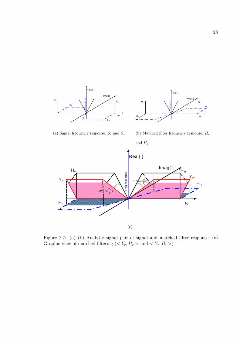
3.2.1 Power Efficiency of Conventional ADC Architectures . . . . . 623.2.2 Asynchronous Processing . . . . . . . . . . . . . . . . . . . . . 663.2.3 Architecture . . . . . . . . . . . . . . . . . . . . . . . . . . . . 71
3.3 Circuit Implementation Details . . . . . . . . . . . . . . . . . . . . . 733.3.1 Dynamic Comparator and Ready Signal . . . . . . . . . . . . 733.3.2 Non-Binary Successive Approximation Review . . . . . . . . . 753.3.3 Series Non-Binary Capacitive Ladder . . . . . . . . . . . . . . 773.3.4 Digital Calibration Scheme . . . . . . . . . . . . . . . . . . . . 803.3.5 Variable Duty-Cycled Clock . . . . . . . . . . . . . . . . . . . 833.3.6 High-Speed Digital Logic . . . . . . . . . . . . . . . . . . . . . 85
3.4 Measured Results . . . . . . . . . . . . . . . . . . . . . . . . . . . . . 853.5 Applicability . . . . . . . . . . . . . . . . . . . . . . . . . . . . . . . . 91
3.5.1 Technology Scaling . . . . . . . . . . . . . . . . . . . . . . . . 913.5.2 Future Role of the Proposed ADC Topology . . . . . . . . . . 93
3.6 Conclusion . . . . . . . . . . . . . . . . . . . . . . . . . . . . . . . . . 95
4 Conclusion and Future Work 97
Bibliography 100

iii
List of Figures
1.1 Time and frequency domain comparisons of ultra-wideband and nar-rowband signals. . . . . . . . . . . . . . . . . . . . . . . . . . . . . . 3
1.2 FCC regulations of indoor communications . . . . . . . . . . . . . . . 5
2.1 Radio architectures. . . . . . . . . . . . . . . . . . . . . . . . . . . . . 122.2 Signal and noise spectrum (left) before and (right) after sub-sampling.
The black color is wanted signal, and the gray one represents noise,assuming a sufficient out-of-band blocking. . . . . . . . . . . . . . . . 14
2.3 Simplified receiver path for direct-conversion (top) and subsampling(bottom) architecture. . . . . . . . . . . . . . . . . . . . . . . . . . . 16
2.4 Bandpass pulse (top left) and subsampled waveform with 0Ts (topright), 0.05Ts (bottom left), 0.1Ts (bottom right) sampling offset. . . 18
2.5 (a) Magnitude response over [0,π] of FIR Hilbert transformer, back-ward, central, and FIR differentiator; (b)–(e) 21-tap FIR of Hilbert anddifferentiator operator on Gaussian and modulated Gaussian pulses(b) Hilbert on Gaussian pulse (c) Differentiator on Gaussian pulse (d)Hilbert of modulated Gaussian pulse (e) Differentiator on modulatedGaussian pulse . . . . . . . . . . . . . . . . . . . . . . . . . . . . . . 23
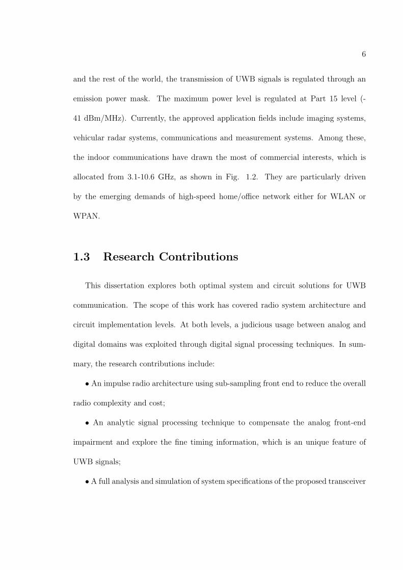
2.6 Datapath of the proposed digital baseband . . . . . . . . . . . . . . 242.7 (a)–(b) Analytic signal pair of signal and matched filter response; (c)
Graphic view of matched filtering (< Yr, Hr > and < Yr, Hi >) . . . 282.8 Detection performance for analytic matched filter. . . . . . . . . . . . 342.9 (a) Plots of analytic matched filter outputs corresponding to {0,5,10,15}%
of Ts timing offset (b)–(c) SNR of real, imaginary, magnitude part ofmatched filter output with 0 to 1 Ts timing offset with high and lowSNR. . . . . . . . . . . . . . . . . . . . . . . . . . . . . . . . . . . . 37
2.10 Trajectory of analytic matched filter output as delay varies. . . . . . . 382.11 (a) Measured noise and interference using TEM horn antenna; (b)
Spectrum after 8th order Butterworth bandpass filter. . . . . . . . . 412.12 Block diagrams of a digital baseband for 0-1 GHz impulse radio. . . . 47

iv
2.13 Flow charts of the digital design flow. . . . . . . . . . . . . . . . . . . 482.14 Graphic view of the digital design flow. . . . . . . . . . . . . . . . . . 492.15 Layout view of the digital baseband. . . . . . . . . . . . . . . . . . . 502.16 Power efficiency comparisons. . . . . . . . . . . . . . . . . . . . . . . 512.17 (a) Power (b) Area pie charts of the digital baseband. . . . . . . . . 522.18 Implementation loss versus input SNR and ADC bits. . . . . . . . . . 542.19 Implementation loss versus input SNR and jitter. . . . . . . . . . . . 552.20 Implementation loss versus in-band interference level and ADC bits. . 562.21 (a) Experiment setup; (b)–(c) Local oscillator frequency mismatch ef-
fect; (d)–(e) Measurements with various distance . . . . . . . . . . . 58
3.1 Conventional architectures for Nyquist ADCs. . . . . . . . . . . . . . 633.2 Synchronous conversion for SAR ADCs. . . . . . . . . . . . . . . . . 653.3 Asynchronous processing concept. . . . . . . . . . . . . . . . . . . . . 653.4 Best (solid line) and worst (dash line) case of Vres profile . . . . . . . 683.5 Simplified block diagrams of the ADC architecture. . . . . . . . . . . 713.6 Dynamic comparator schematic. . . . . . . . . . . . . . . . . . . . . . 733.7 Conventional implementation of radix creation. . . . . . . . . . . . . 763.8 Series Non-binary Capacitive Ladder. . . . . . . . . . . . . . . . . . . 783.9 LMS calibration loop. . . . . . . . . . . . . . . . . . . . . . . . . . . . 823.10 Variable duty-cycled clock generation. . . . . . . . . . . . . . . . . . . 843.11 DNL and INL before and after combining weights calibration. . . . . 863.12 PCB for testing Nyquist frequencies. . . . . . . . . . . . . . . . . . . 873.13 DNL and INL before and after combining weights calibration. . . . . 883.14 Measured SNDR versus fs and fin for single ADC (a) below and (b)
above Nyquist frequency. . . . . . . . . . . . . . . . . . . . . . . . . . 893.15 (a) Measured SNDR versus fs and fin for time-interleaved ADC and
its (b) FFT spectrum measured at 159 MHz input. . . . . . . . . . . 903.16 FFT spectrum before and after clock skew calibration. . . . . . . . . 913.17 Future role of the SA architecture. . . . . . . . . . . . . . . . . . . . 943.18 FOM comparisons with recent >10 MHz, 6-8 bit ADCs from ISSCC
00-05. . . . . . . . . . . . . . . . . . . . . . . . . . . . . . . . . . . . 95

v
List of Tables
3.1 Performance Summary (25 ◦C) . . . . . . . . . . . . . . . . . . . . . 923.2 Technology Scaling on the proposed ADC architecture . . . . . . . . 93

vi
Acknowledgments
First of all, I am truly grateful to my advisor, Prof. Bob Brodersen, for his support,
encouragement and advice over the past years. I have been benefited not only from
his vision but also his unique philosophies of handling things, which will become
invaluable treasures in my life. I am indeed fortunate to pursue MS and PhD degrees
with him. Additionally, BWRC created by him and Prof. Jan Rabaey has been a
great place to grow as a graduate student.
I’d like to thank Prof. Borivoje Nikolic for his informative digital classes, feedback
on my thesis and chairing my qualifying exam committee. I’d also like to thank
Prof. Paul Wright for spending his time being my dissertation committee. Thanks
to Prof. David Tse and Prof. Kannan Ramchandran, I have learned fundamental
communication and DSP background in the early graduate school years. I’d like to
thank Prof. Paul Gray for discussing with my PhD project.
There are, of course, other graduate students who add more flavors to my life in
BWRC. First of all, my special thanks go to Jeff Ou, who found my application pack-
age was lost before I could even come to Berkeley. Ian O’Donnell led the first project
when I joined the group. We had countless technical and non-technical discussions
which I truly learned from him. His sense of humor and travel advice made my life
in Berkeley enjoyable. Thanks, Ian. Thanks to Stanley Wang, we have survived
many class projects together. His technical comments and experience sharing have
been very helpful ever since we joined the group. My thanks also go to Luns Tee,

vii
who offered me many useful technical discussions regarding my PhD project. With
his company, we were able to go on car-pool lanes whenever we went down to south
bay to fix our board and packaging problems. Engling Yeo has been kindly helping
me with digital tool issues in the early days, and joined me with many bike rides
and other outdoor activities. Tufan Karalar, Axel Berny and Tim Wongkomet who
started graduate school at the same year with me. It has been great to take classes,
exams with them and exchange our experiences at different stages of the graduate
school. Tufan and I ended up sitting next to each other. I’d also thank Bill Tsang
for useful discussions and being a great listener when I had to complain about testing
and layout stuffs. I’d thank Liang-Teck Pang for sharing the laboratory test bench
with me while he was away for an internship.
There are other graduate students who overlapped with my years and I am thank-
ful for their advice and being great neighbors in BWRC. They are Yun Chiu, Ada
Poon, Johan Vanderhaegen, Changchun Shi, Yuen-Hui Chee, Chinh Doan, Brian
Limketkai, Henry Jen, Dejan Markovic, En-Yi Lin and Sayf Alalusi.
Without these great BWRC staffs, there is no way I could get any project going.
They are Tom Boot, Gary Kelson, Elise Mills, Brian Richards, Kevin Zimmerman,
and Sue Mellers.
My thanks to Shiang-Lung Koo, I have been travelling around most of the places
with his company ever since I came to Berkeley, and he is always there whenever I
need help including any car problem. I also thank him along with Yuan-Shih Chen

viii
and Luns Tee for our regular Friday night dinners.
Last but not the least, I am greatly indebted to my family. My parents, Chia-
Shun Chen and Shu-Mei Huang, have given me their wholehearted support and care
through every stage of my life. My brother, Wei-Ming Chen, has always been my
best buddy. I am also grateful for the support and blessings from my parents in law,
Chia-Ming Lee and Huei-Huei Hsueh. Undoubtedly, without the unreserved love,
support and care from my wife, Wan-Hsuan Lee, there is no way I could reach this
point. I am truly fortunate to have you in my life, Wan!

1
Chapter 1
Introduction
1.1 Trends in Wireless Communication Systems
The rapid development of the wireless systems has closely linked with our daily
life. From outdoor cellular systems to indoor office/home network, the wireless
technologies are ubiquitous. Among these, the regulatory allocation of unlicensed
bandwidth particularly triggers a wide range of applications from personal area to
metropolitan area network. The WLAN systems are successful examples, such as
IEEE 802.11a/b/g, to provide data network in office or home environment. The data
capacity has been increasing using more efficient modulation schemes or multiple an-
tenna arrays as proposed in IEEE 802.11n. In the WMAN area, 802.16 has been
standardized to provide a high-rate wireless link in wider area. For the personal area
(WPAN), the high-speed link is also of interest to replace the cable connections, as

2
seen in 802.15 efforts. Regardless of which application, the trend of these emerging
wireless systems has been demanding more bandwidth, increased data rate, and more
configurability to accommodate multi-standards. However, the power consumption
is tightly constrained to enable mobile deployment for longer battery life. Especially,
those systems without high data rate constraint, such as sensor networks and RFIDs,
would most likely require extremely low cost and low power consumption.
This trend has driven the radio implementation into a new era. Previously, the
radio was normally optimized for a particular signal band, which is no longer ade-
quate for the future wideband radios. From the radio architecture perspective, there
is always a tradeoff between the amount of processing in analog and digital domains.
The most critical factor that often determines this tradeoff is analog-to-digital con-
verter (ADC). The wide signal bandwidth implies a high sampling rate of ADC, and
more dynamic range (DR) can be required if less analog processing is done prior to
ADC. From circuit implementation perspective, the digital baseband processing is
less an issue since the scaled technology keeps favoring the digital world. However,
the RF power amplifier needs enhancement of its linearity and dynamic range in order
to maintain the flexibility for multi-standards. The antenna requires a wider band-
width and optimized in those communication bands. Similarly, the receiver front-end
components before frequency translation, i.e. mixers, have to cover the wide RF
bandwidth and sometimes are tuned to several communication modes. Finally, the
implementation cost of a high-speed high-DR ADC can be exorbitant so that a mod-

3
• Ultra-Wideband (impulse) • Narrowband
Time
Freq.
Time
Freq.FcFc
BW
Figure 1.1: Time and frequency domain comparisons of ultra-wideband and narrow-band signals.
ification of radio architecture is needed to relax the ADC specifications for an overall
lower cost. On the other hand, a new wave of pushing ADC performance has been
underway, which will give more freedom for different radio architectures.
These challenges have rendered engineers a new playground from both system and
component designs. A co-design of system and circuit level becomes crucial especially
a system-on-chip (SOC) solution is a key to dramatically cut down the cost. This
thesis is one example of these new opportunities. We will explore both system and
circuit spaces for ultra-wideband communication.

4
1.2 Overview of Ultra-Wideband Communication
An ultra-wideband signal has been widely used in radar applications. Recently, the
usage of such a signal was approved by FCC [1] in 2002. According to the definitions
by FCC, any signal with an absolute bandwidth or relative bandwidth (ratio of signal
bandwidth and center frequency) greater than 500 MHz and 25% respectively is
considered as an ultra-wideband signal. Comparing to a narrowband signal, an UWB
signal concentrates only a small duration in time, while its frequency spectrum is
widely spread, as shown in Fig. 1.1. Due to the different signal characteristics, it
owns different design issues from both communication and circuit implementation
perspectives. For example, the channel diversity of a wideband signal increases with
the bandwidth, i.e. more resolvable multi-paths. Moreover, the narrow pulse duration
also implies a fine timing information. Based on these unique features, the scope of
utilizing UWB has covered both high and low end applications as seen in 802.15 UWB
standardization efforts. High-speed application includes multimedia communications,
home networking, wireless USB and wireless data network. The data rate is on the
order of hundreds of Mbps with a power consumption of hundreds of milli-watts. For
a lower speed application, precision ranging, sensor network and tracking systems are
of high interests. The data rate normally requires tens of Kbps with a mere power
consumption of mW.
There has been a great concern of harmful interferences with the existing wireless
systems after deploying UWB devices. To ensure the peaceful coexistence of UWB

5
Figure 1.2: FCC regulations of indoor communications
6
and the rest of the world, the transmission of UWB signals is regulated through an
emission power mask. The maximum power level is regulated at Part 15 level (-
41 dBm/MHz). Currently, the approved application fields include imaging systems,
vehicular radar systems, communications and measurement systems. Among these,
the indoor communications have drawn the most of commercial interests, which is
allocated from 3.1-10.6 GHz, as shown in Fig. 1.2. They are particularly driven
by the emerging demands of high-speed home/office network either for WLAN or
WPAN.
1.3 Research Contributions
This dissertation explores both optimal system and circuit solutions for UWB
communication. The scope of this work has covered radio system architecture and
circuit implementation levels. At both levels, a judicious usage between analog and
digital domains was exploited through digital signal processing techniques. In sum-
mary, the research contributions include:
• An impulse radio architecture using sub-sampling front end to reduce the overall
radio complexity and cost;
• An analytic signal processing technique to compensate the analog front-end
impairment and explore the fine timing information, which is an unique feature of
UWB signals;
• A full analysis and simulation of system specifications of the proposed transceiver

7
architecture;
• An asynchronous ADC architecture to achieve outstanding power efficiency of
a high-speed, medium-resolution ADC;
• A series, non-binary capacitive ladder to enable high-speed operation, low-power
consumption and high input bandwidth while creating arbitrary radix for the search-
ing schemes;
• A digital calibration scheme to compensate the defects of manufacturing process,
which can be extended for higher-resolution ADCs.
1.4 Thesis Organizations
Chapter 2 focuses on the system-level work, including radio architecture compar-
isons, analog front-end and digital signal processing and baseband blocks. The system
specifications and prototype are also discussed. In chapter 3, the asynchronous ADC
architecture is proposed and described in details. The prototype design in 0.13µm
CMOS and its measured results are provided. The future extension and potential
usage of this ADC architecture are discussed in the end. Finally, the conclusions and
future work are summarized in Chapter 4.

8
Chapter 2
Sub-sampling UWB system
architecture
In this chapter, an impulse radio architecture utilizing a simple analog front-end
along with digital complex signal processing is proposed to allow a low complex-
ity implementation of a 3.1-10.6 GHz Ultra-Wideband radio. The proposed system
transmits passband pulses using a pulser and antenna, and the receiver front-end
down-converts the signal frequency via sub-sampling, thus, requiring substantially less
hardware than the existing direct conversion approach. After analog-to-digital con-
verter (ADC), the signal is projected into complex signal domain to perform matched
filtering to not only mitigate the timing sensitivity induced by analog circuit impair-
ment, but also extract the fine time resolution provided by the wideband nature of a
UWB signal. The performance and potential usages of these complex signal process-

9
ing blocks are solved and compared with different complex signal transformations.
Based on the proposed architecture, the system specifications and implementation
issues are further analyzed and emulated with system-level simulations with mea-
sured signal and noise. Finally, a prototype is built with discrete components to
demonstrate the feasibility of the proposed impulse radio architecture.
2.1 Introduction
Ultra-wideband (UWB) transmission was approved by the FCC in 2002 [1] for
several frequency bands (0-960 MHz, 3.1-10.6 GHz and 22-29 GHz), and has since
drawn considerable attention for a variety of applications, including imaging, surveil-
lance, high-speed data communication and high-resolution locationing [2][3]. One
of the most discussed applications is indoor communication systems operated in the
frequency band from 3.1 to 10.6 GHz. The main interest lies in high-speed (100s’
of Mb/s) and short-range (less than 10 meters) systems for wireless personal area
network (WPAN). On the other extreme, low data rate (10s’ Kb/s) communications
are also of interest, such as sensor network and ranging system.
The new challenge for UWB radio implementation is to fully exploit the wideband
nature for lower power and a less costly solution than by increasing the efficiency of
narrowband techniques such as occurring in the standard 802.11n. While most of the
published UWB implementations [4][5][6][7][8] are supporting the MultiBand OFDM
approach, i.e. WiMedia Alliance [9], these radios are essentially a scaled up version

10
of the current 802.11a/g systems, which results in considerable complexity in their
implementations.
In this thesis, we have explored the new signalling opportunity using non-sinusoidal
carriers, so called impulse radios [10][11], which allowed us to take a fundamentally
new approach to radio architectures, signal processing techniques, and analog circuits.
Our goal is to take the benefit of the wideband characteristics of UWB pulses and
seek a system solution which dramatically cuts down the implementation cost while
exploring the inherent capability of fine-timing resolution.
For the radio architecture, we proposed to utilize a sub-sampling analog frontend
for reduced component count and to provide as much processing as possible in the
digital domain to realize a substantial reduction of power and area [12]. The chal-
lenges of the simplified frontend are identified and suitability for the UWB case is
justified from system performance and circuit implementation perspectives. One key
issue of sub-sampling an RF signal is timing sensitivity, and this problem is mitigated
by exploring several signal transformations of the sampled UWB signal in the digital
domain. Among them, the use of analytic signalling provides significant performance
improvements in wideband signal processing as is the case in UWB. The performance
and properties of the proposed analytic signal processing blocks were analyzed and
shown to be useful for synchronization, data detection and fine timing extraction for
ranging applications. Given the proposed system architecture, the implementation
specifications and issues were further explored with the assistance of system simula-

11
tions. In addition, a recently developed low-power and high-speed ADC that is able to
sub-sample above 4 GHz signal band [13] makes the proposed sub-sampling front-end
practical. Finally, the proposed sub-sampling impulse radio was validated through
a real wireless link using an experimental transceiver composed of UWB antenna,
filters, pulse generator and high-speed sampling oscilloscope.
The thesis is organized as follows. Section 2.2 compares the implementation com-
plexity of the proposed transceiver architecture and the conventional direct-conversion
one. Section 2.3 provides an overview of sub-sampling and explains its implementa-
tion challenges and justifies the applicability for UWB. Section 2.4 focuses on the
digital complex signal processing of a UWB signal. The properties and usage of sev-
eral critical complex signal processing blocks are analyzed. Section 2.5 provides a
link budget analysis to determine system specification and identifies implementation
issues. Next, system-level simulations using measured pulse shape and noise samples
are performed to verify system specifications and tradeoffs in section 2.6. Finally, a
prototype is built and measured to prove the concept in section 2.7.
2.2 Comparison of Transceiver Architectures
The proposed system is based on the impulse radio approach [10][11]. Many
recent published UWB system solutions [4][5][14][6][7][8], including both OFDM and
DSSS approaches, have adopted a direct-conversion architecture, as shown in Fig.
2.1(a). A major challenge of this approach is that the overall complexity still remains

12
UWB attenna
BpLNA
Digital Backend
90 shift
ADC
ADC
90 shift
Bp
I
Q
PA
DAC
DAC
(a) Direct-conversion radio architecture
Bp
UWB attenna
Bp
LNA
ADC
Digital Backend
Pulser
(b) Sub-sampling radio architecture
Figure 2.1: Radio architectures.
high which means a dramatic cost and power reduction from the current wireless
solutions is unlikely. For example, the transmitter of a wideband OFDM radio requires
high-speed digital-to-analog converter, up-conversion mixers, oscillators and power
amplifier with linearity and peak-to-average ratio (PAR) constraints because of the
multicarrier transmission [15]. On the other hand, an impulse radio simply uses a
pulser to drive the antenna, and radiates a passband pulse shaped by the response
of the wideband antenna and any possible bandpass filter, as shown in Fig. 2.1(b).
The hardware elimination of mixers and local oscillators for mixing and the reduced
linearity requirement imply lower complexity implementations of a transmitter.
On the receiver side, the direct-conversion architecture utilizes two paths (I and Q)
of local oscillator (LO), frequency synthesizer and mixer to down-convert the passband

13
signal to baseband prior to the ADCs. According to the published literatures, these
extra analog circuit blocks for frequency translation can contribute significant portion
of the total power consumption. Alternatively, the frequency translation can be
done in the sampling process, using sub-sampling, as a part of ADC. This results
in only one receive path and dramatically reduces the component count compared
to a direct-conversion architecture. The remaining analog blocks prior to the ADC
are amplifiers and bandpass filters. The sampled data are processed by a digital
matched filter in order to reach the matched filter bound for optimal detection [16].
The proposed system avoids wideband analog processing by adding more processing
to the digital backend, which results in a more efficient solution. Moreover, the single
analog receiving path eliminates the analog I/Q mismatch problem caused by the
variability of IC fabrication.
2.3 Analog: Subsampling Front End
In this section we will first review the fundamentals of subsampling theory and
then discuss what makes it a promising solution for ultra-wideband systems.
2.3.1 Theory Background and Challenges
A Subsampling front end directly samples the passband signal at twice the signal
bandwidth instead of the maximum signal frequency. The signal is bandlimited from

14
FsF
req
resp
onse
Fl Fh
B
Fre
q re
spon
se
ππππ-ππππ
Figure 2.2: Signal and noise spectrum (left) before and (right) after sub-sampling.The black color is wanted signal, and the gray one represents noise, assuming asufficient out-of-band blocking.
Fl to Fh (Hz), and the sampling frequency is Fs (Hz). By carefully choosing Fs, Fl
and Fh, a non-aliased sampled spectrum can be derived [17]. For example, if the
lower or upper frequency bound, i.e. Fl and Fh, is a non-negative integer multiple of
the signal bandwidth, B, the signal aliasing can be avoided at the minimal uniform
sampling rate, 2B,
Fl = n · (Fh − Fl) = n ·B, (2.1)
where n ∈ N .
The undersampling ratio, K, is defined as, bFh/2Bc, the largest integer but smaller
than bFh/2Bc. This ratio is a good indication of the amount of aliasing effect, which
will be seen later.
There are several key challenges about subsampling that prohibit it from being
popular in existing narrowband systems. First of all, the noise spectrum from −Fl to
+Fl will alias into the signal band and thus deteriorate the passband SNR, assuming

15
the receiver bandwidth is Fh. Even if the receiver can afford a perfect anti-aliasing
filter, the circuits after the filter, such as the sample and hold or buffer stages, still
contribute thermal noise. Therefore, if the receiver noise is dominated by these circuit
noise sources, the passband SNR degradation is proportional to the undersampling
ratio ,K, which can be on the order of hundred’s for a narrowband system. The higher
the undersampling ratio is, the harder it is to implement the anti-aliasing filter, which
will be elaborated in the system specification section. Secondly, it is more difficult
to design a good bandpass (anti-aliasing) filter at RF frequency band than IF or
baseband. As mentioned earlier, insufficient attenuation of out of band noise causes
more degradation in signal SNR. Traditionally, these high Q bandpass filters are
implemented off-chip, which unavoidably increases the cost and power consumption.
Finally, the incoming signal frequency is actually higher than the sampling frequency;
therefore the receiver’s tracking bandwidth needs to cover the maximum signal fre-
quency range and sampling jitter causes even more degradation of the SNR. If one
models the jitter-induced error as another noise source, the noise power increases
with input signal frequency [18]. Therefore, directly sampling at the RF frequency
introduces more noise power than at an IF or baseband.
2.3.2 Subsampling for UWB
Interestingly, the challenge of subsampling is relaxed in the UWB case due to its
wide signal bandwidth. For example, if a 1 GHz wide pulse is transmitted between 3

16
gm
RL
fcfs
gm
RL
fs
CL
CL/K
B
B*K
Digital
Digital
Figure 2.3: Simplified receiver path for direct-conversion (top) and subsampling (bot-tom) architecture.
to 4 GHz, and sampled at 2 Gsa/s, then the undersampling ratio is only two, much
smaller than any narrowband system. A simplified receiver path of direct-conversion
and subsampling architecture is shown in Fig. 2.3 to illustrate the impact of the
undersampling ratio, K, on the noise folding issue. The out-of-band noise prior to
anti-aliasing (AA) filer should be blocked by the filter response, which sets the same
out-of-band attenuation constraints of the two radio architectures. We will discuss
the specification of AA filter response for the subsampling frontend in section 2.5.
Here, we assume an ideal anti-aliasing filter and focus on the noise from the following
circuits, composed of a buffer stage and track-and-hold. The main difference between
the two architectures is that the subsampling frontend needs to maintain a high band-
width up to the sampling circuit. Therefore, the wider thermal noise spectrum post

17
AA filter will fold into signal band after sampling. In this case, a simple buffer stage is
modelled as a transconductance (gm) cell and loaded by RL. Considering the thermal
noise from active devices (4kTγgm V2/Hz) and resistors (4kTR V2/Hz), the total
noise sampled onto the capacitor can be derived as, (1 + γgmRL) kTCL
for the direct-
conversion architecture, and as (1+γgmRL) kTCL·K for subsampling one, indicating that
a smaller undersampling ratio reduces the amount of extra noise folding. Moreover,
UWB has a relatively lower received SNR due to limited signal transmission power
regulated by FCC and larger in-band noise power, as the large signal bandwidth takes
in more ambient noise, early-stage circuit noise power and possible interference. This
means the UWB receiver requires only a moderate resolution ADC (4-6 bits), as will
be further analyzed in later sections. For such ADCs, the quantization noise domi-
nates over the sampled thermal noise on the sampling capacitor. In other words, the
small sampling capacitor does not noticeably degrade the overall system performance,
which makes subsampling architecture very promising for UWB.
Next, the difficulty of implementing a RF bandpass filter is also relaxed by the
lower filter Q, which is less than ten in UWB, enabling the integration in a CMOS
implementation. Note that the use of a high-Q notch filter can be required in the
case of a strong interference close to the signal band. In section 2.5, more detailed
discussion of bandpass filtering will be provided. Lastly, the lower ADC dynamic
range due to large in-band noise and vulnerability to interference will reduce the
sampling jitter constraint. Our system level simulations in section 2.6 also verify the

18
0 0.5 1 1.5 2
x 10-8
-1
0
1
x 10-4 bandlimited pulse
0 0.5 1 1.5 2
x 10-8
-1
0
1
x 10-4 offset=0Ts
0 0.5 1 1.5 2
x 10-8
-1
0
1
x 10-4 offset=0.05Ts
0 0.5 1 1.5 2
x 10-8
-1
0
1
x 10-4 offset=0.1Ts
Figure 2.4: Bandpass pulse (top left) and subsampled waveform with 0Ts (top right),0.05Ts (bottom left), 0.1Ts (bottom right) sampling offset.
relatively lower dynamic range requirements.
2.3.3 Timing Sensitivity Issue
While subsampling from the noise standpoint is feasible for UWB, the architec-
ture also suffers from sampling offset, which is introduced by frequency and phase
mismatch between the TX and RX oscillators or changes of pulse arrival times. The
sampled waveform will change dramatically due to this sampling offset, which can
cause serious performance degradation of a receiver using matched filtering approach.

19
It is known that the use of a matched filter [16] results in the optimal SNR perfor-
mance when the matched filter response perfectly matched to the incoming signal.
However, if there is any mismatch between the two, the system performance will be
deteriorated as derived in [19]. In this case, the mismatch is caused by the varied
sampled waveform due to timing offset, which will be referred as a timing sensitivity
issue in the following contents. In fact, the timing sensitivity is more significant in
subsampling than Nyquist sampling given the same sampling frequency, since the
variation in the waveform significantly complicates the design of digital matched fil-
ter. Using measured UWB pulses that are bandlimited to 3-4 GHz, the impact of
sampling offset on sampled waveform is shown in Fig. 2.4. An analytic signaling
approach described in the next section is thus proposed to alleviate this problem.
2.4 Digital: Complex Signal Processing
In order to fully exploit the wideband nature of UWB signal, we need to analyze
the signal in the appropriate space. Due to the wide band frequency content, the UWB
pulses possess fine timing information while it increases synchronization difficulties
as described previously, especially for a subsampling analog front-end. From the
ranging/locationing perspective, this fine timing resolution is very helpful.

20
2.4.1 Complex representations of UWB signals
To understand the timing information extraction, we purposely inject a timing
offset into the incoming signal and observe the change in the frequency domain.
Equation (2.2) shows a bandlimited signal, s(t), which is sampled at the sampling
rate, 1/Ts. Any sampling offset, To, of the sampling sequence will transform into a
phase shift, e−jk 2πTs
To , in the frequency domain.
s(t) ·∑
δ(t− k · Ts − To)F .T .⇐⇒ S(ω) ∗
∑δ(ω − k
2π
Ts
) · e−jk 2πTs
To . (2.2)
The key to study phase information is to project the signal into an orthogonal
space, which is a 90-degree phase shift in this case. In a narrowband system, sine
and cosine carrier is used to develop I and Q channels. However, for an UWB signal,
the orthogonality at one particular frequency is not good enough, so a wideband
phase shifter is required. Two possibilities are Hilbert transformer (H[·]) and the
differentiator (D[·]). A wideband 90-degree phase shift is thus obtained, as seen in
their ideal frequency responses, (2.3) and (2.4).
H[s(t)] =1
πt∗ s(t)
F .T .⇐⇒ −j · sign(ω) · S(ω) (2.3)
where sign() is the signum function.
D[s(t)] =d
dt· s(t) F .T .⇐⇒ j · ω · S(ω) (2.4)

21
Note that, in both cases, 90-degree phase shift is independent of the frequency.
For a narrowband signal, like sin(ωot), the two operators are almost identical except
for a constant gain difference, because H(sin(ωot)) = cos(ωot) while D(sin(ωot)) =
ωo · cos(ωot). However, in the wideband signal case, the differentiator suffers from a
non-flat gain response (proportional to frequency) as seen in (2.4), which will not only
introduce signal distortion, but also enhance the unwanted noise at high frequency.
In contrast, an ideal Hilbert transformer has unity gain over the entire spectrum, i.e.
no signal distortion.
To implement these operations in digital baseband, we take a further look into
the discrete Hilbert transformer and differentiator. As an example, we designed an
equal-ripple 21-tap FIR filter using the Parks-McClellan algorithm to obtain an exact
90-degree phase shift for the Hilbert transformer [20]. For the differentiator, we used
a backward difference approximation (y[n] = x[n]− x[n− 1]), and central difference
approximation (y[n] = (x[n+1]−x[n−1])/2) for their simplicity in computation. We
also design another 21-tap FIR filter for the differentiator using the Parks-McClellan
algorithm. The phase response of these discrete-time implementations all remain 90
degrees with Figure 2.5(a) showing the magnitude response of these filters.
With these phase shifters in hand, the orthogonal bases can be constructed into
a complex signal. By combining a Hilbert transformed signal, a single-side banded
(SSB) spectrum, i.e. analytic signal, is derived,

22
y(t) = s(t) + j · H(s(t)). (2.5)
Similarly, for a narrowband signal centered at ωo, a complex signal, which is an
approximation of the analytic signal, can be formulated as,
y(t) = s(t) + j · 1
ωo
D(s(t)). (2.6)
To better understand what these complex signal represents in the case of UWB
pulses, we apply these transformations for both baseband and passband wideband
signal, since FCC allows the use of both DC-1 GHz and 3-10 GHz frequency bands.
Figure 2.5(b)–(e) shows the real and imaginary part of the transformed complex
signal and its magnitude and phase information using a 21-tap FIR filter. Due to
the large passband ripple in the frequency response, using a differentiator approach
causes more pulse distortion. For preserving the shape and energy of a wideband
signal, the discrete Hilbert transformer is preferred.
2.4.2 Proposed digital baseband using complex signaling
Figure 2.6 shows the datapath of the proposed digital baseband. The main com-
ponents are an analytic signal transformer, pulse shape estimator, correlators, ana-
lytic matched filter, and detection block. For optimal detection, sufficient statistics
is achieved by projecting onto the signal dimension through pulse matched filtering
whose filter response requires an estimation block. The following correlators are used

23
0 0.5 1 1.5 2 2.5 30
0.2
0.4
0.6
0.8
1
1.2
1.4
1.6
1.8
2
Mag
nitu
de (
abs)
Frequency (rad/sec)
Backward diff.
Central diff.
FIR Hilbert
FIR diff.
(a)
0 20 40 60 80 100−20
0
20
40Hilbert Pair of the Gaussian Pulse (FIR Hilbert)
RealImag
0 20 40 60 80 1000
10
20
30
40
Mag
nitu
de
0 20 40 60 80 100−2
−1
0
1
2
Pha
se
FIR Hilbert mag.FIR Hilbert angleGaussian Pulse
(b)
0 20 40 60 80 100−20
0
20
40Differentiator Pair of the Gaussian Pulse (FIR diff.)
RealImag
0 20 40 60 80 1000
10
20
30
40
Mag
nitu
de
0 20 40 60 80 100−2
−1
0
1
2
Pha
se
FIR diff. magFIR diff. angleGaussian Pulse
(c)
0 10 20 30 40 50 60 70 80 90−40
−20
0
20
40Hilbert Pair of the Modulated Gaussian Pulse (FIR Hilbert)
RealImag
0 10 20 30 40 50 60 70 80 90
0
10
20
30
40
Mag
nitu
de
0 10 20 30 40 50 60 70 80 90−4
−2
0
2
4
Pha
se
FIR Hilbert mag.FIR Hilbert angleModulated Gaussian Pulse
(d)
0 10 20 30 40 50 60 70 80 90−40
−20
0
20
40Differentiator Pair of the Modulated Gaussian Pulse (FIR diff.)
RealImag
0 10 20 30 40 50 60 70 80 90
0
10
20
30
40
Mag
nitu
de
0 10 20 30 40 50 60 70 80 90−4
−2
0
2
4
Pha
se
FIR diff. magFIR diff. angleModulated Gaussian Pulse
(e)
Figure 2.5: (a) Magnitude response over [0,π] of FIR Hilbert transformer, backward,central, and FIR differentiator; (b)–(e) 21-tap FIR of Hilbert and differentiator op-erator on Gaussian and modulated Gaussian pulses (b) Hilbert on Gaussian pulse(c) Differentiator on Gaussian pulse (d) Hilbert of modulated Gaussian pulse (e)Differentiator on modulated Gaussian pulse

24
ADC
AnalyticMF
AnalyticSignal
Transform
PulseShape
EstC
orrela
tors
Detect(Cordic)
Figure 2.6: Datapath of the proposed digital baseband
to provide more processing gain if necessary or despread any possible modulated code.
Finally, a detection block makes use of the analytic matched filter outputs to decode
the data or extract timing information for ranging purpose. Several critical processing
blocks will be discussed in this section.
Analytic signal transformer
The analytic signal transformation can be implemented using FIR Hilbert trans-
former or FFT processor. With the FFT approach, one can potentially eliminate
in-band tones before the detection block with the penalty of more implementation
complexity. From the system simulations, using a 21-tap FIR Hilbert transformer
degrades SNR by less than 1 dB compared to ideal analytic signal transformation.

25
Pulse shape estimator
To make an optimal detection, the pulse matched filter response is required as a
priori information. However, due to the varying wireless channel response and antenna
pattern, the received pulse shape needs an estimation by the receiver before decoding
data. In the proposed baseband processing, a maximum likelihood (ML) estimator
is used for the shape estimation without any prior information. It is assumed that
a training sequence spread with a pseudo random (PN) code is transmitted within
the coherence time of the channel. The modulated pulses are spaced far enough to
avoid inter-symbol interference during training phase. The estimator can be derived
as follows.
The ith symbol of the incoming signal to the ML estimator is expressed as a 1×n
vector, ~yi.
~yi = [y(1)i y
(2)i . . . y
(n)i ] = ci · ~S + ci ·~Ii + ~Ni, (2.7)
where ~S = [s(1)s(2) . . . s(n)] is the received pulse shape (assumed constant within
channel coherence time), ~Ii is the sum of the interfers, ~Ni is the sum of all the additive
Gaussian noise sources, and ci is the ith chip of PN code.
Therefore, the received samples over the entire PN code is Y =
~y1
~y2
...
~ym
, and the

26
ML estimation of ~S is
~SML = argmaxb~S P (Y | ~S = [s(1)s(2) . . . s(n)])
⇒ s(j)ML = argmaxbs(j)
P (
y(j)1
y(j)2
...
y(j)m
| s(j)),∀j ∈ [1 . . . n]. (2.8)
Since the sum of interfers is despreaded with a PN code, the aggregate noise
samples are modelled as white Gaussian noise. We also consider a LO frequency
offset, ∆f , between Tx and Rx, which causes the sampling error term −iks′(j) as
shown in Eq. (2.9), assuming k ∝ ∆f , and is so small that first-order approximation
of sampling error is sufficient.
ci · ~I(j)i + ~N
(j)i ∼ N (0, σ2
I + σ2N), ∀i, j.
⇒ P (
y(j)1
y(j)2
...
y(j)m
| s(j)) =m∏
i=1
1√2π(σ2
I + σ2N)· exp
−[(ciy
(j)i−s(j)−iks
′(j))22(σ2
I+σ2
N)
](2.9)
Apply Eq. (2.9) back to Eq. (2.8), the estimator can be derived as,

27
∂
∂s(
m∑i=1
(ciy(j)i − s(j) − iks
′(j))2) = 0
⇒ m · s(j)ML +
m(m + 1)
2ks′
(j)
ML =m∑
i=1
ciy(j)i
⇒ s(j)ML =
1
m·
m∑i=1
ciy(j)i + d · e −2
(m+1)ktj
if (m + 1)k ∼ 0 ⇒ ~SML =1
m·
m∑i=1
ci~yi (2.10)
This shows that the sample drift, i.e. (m + 1)k, over the entire training sequence
period due to frequency mismatch must be small to reduce the estimation error term.
The above analysis was done assuming the estimator is prior to the analytic signal
transformation. Eq. (2.10) still holds if the estimator is placed after the complex
signal formulation, since the noise is modelled as complex Gaussian variable and the
rest of the derivations stay the same.
Analytic matched filter
An analytic matched filter is used to achieve optimal performance assuming the
incoming noise is additive and white. The assumption is valid if the circuit and
ambient thermal noise dominate. For the interference dominated case, a whitening
filter, which can be incorporated with analytic signal transformer as mentioned earlier,
is required for optimal performance. To gain more insights about the analytic matched
filter, we derive the expressions of its outputs in continuous time for both noiseless and
noisy cases. Assuming the UWB signal, s(t), is transformed into the analytic signal
28
Si-
Freq
resp
onse
ω
Imag{ }
Real{ }
Sr+
Si+
Sr-
(a) Signal frequency response, Sr and Si
Hi-
Freq
resp
onse
ω
Imag{ }
Real{ }
Hr+
H i+
Hr-
(b) Matched filter frequency response, Hr
and Hi
H i-
Freq
resp
onse
os
TT
kπθ 2=∠
os
TT
kπθ 2−=∠
ω
Imag{ }
Real{ }
Hr+
Yr+
Hi+
Hr-
Yr-
(c)
Figure 2.7: (a)–(b) Analytic signal pair of signal and matched filter response; (c)Graphic view of matched filtering (< Yr, Hr > and < Yr, Hi >)

29
representation, s(t) = sr(t) + j · si(t), the matched filter response is implemented as
h(t) = s∗(T − t) = s∗r(T − t)−j ·s∗i (T − t). We define the impulse response of the filter
as h(t) = hr(t)−j ·hi(t), and thus hr(t) = s∗r(T−t), and hi(t) = s∗i (T−t). As a result,
their Fourier transformed counterparts satisfy Hr(ω) = S∗r (ω) and Hi(ω) = S∗i (ω), as
shown in Fig. 2.7. Note that sr(t), si(t), hr(t), hi(t) are real-valued functions.
Before we proceed with the following analysis, an operator is defined as follows,
< x, y >=
∫ b
a
x(t) · y(T − t)dt, where T = b− a. (2.11)
If the inputs of the analytic matched filter are yr(t) + j · yi(t), its outputs are
expressed as,
mr + j ·mi = < yr + j · yi, hr − j · hi >
= < yr, hr > + < yi, hi > +j · (− < yr, hi > + < yi, hr >).(2.12)
The UWB pulse is assumed to locate between time a and b without inter-symbol
interference.
To understand the properties of the analytic matched filter, three conditions are
considered for Eq. (2.12). We start from an ideal communication channel and grad-
ually add in more non-idealities.
Case I. Noiseless input and perfectly matched timing

30
This is the most ideal case in which incoming signal perfectly matches with the
matched filter response without any noise, i.e. yr = sr, yi = si. The sampling
timing offset between input signal and impulse response is assumed zero. The
output is expressed as,
mr + j ·mi = < sr + j · si, hr − j · hi >
= < sr, hr > + < si, hi > +j · (− < sr, hi > + < si, hr >)
= Er + Ei = 2 · Es (2.13)
,where Er, Ei is the real and imaginary part of signal energy defined as∫ b
as2
r(t)dt
and∫ b
as2
i (t)dt respectively. We assume an ideal analytic transformer, and thus
Er = Ei = Es. Note that sr(t) and hi(t) are orthogonal to each other, therefore
< sr, hi >= 0, and so is < si, hr >= 0. This shows that all the energy concen-
trates in the real part of the analytic matched filter, and thus complex signal
transformations are redundant under the ideal case.
Case II. Noiseless input with timing offset
In this case, we add in a timing offset of To between input signal and matched
filter response while the input is still noiseless. Recall from Eq. (2.2), the timing
offset introduces a phase shift term of e±jk 2πTs
To . The frequency response of the
real part of the received signal is shown in Fig. 2.7(c); Yr±(ω) is rotated by
±k 2πTs
To from Hr±(ω). Since matched filtering is equivalent to image projection

31
in the frequency domain, the projected area represents the absolute value of the
matched filter output. In Fig. 2.7(c), the values of < yr, hr >,< yr, hi > are
shown in the darker and lighter shaded areas. From these graphs, the timing
offset results in a re-distribution of the signal energy between these two terms.
Therefore, a complex signal transformation is necessary in this case, otherwise
the signal energy will be lost under any timing uncertainty. The matched filter
output is re-derived as,
mr + j ·mi = < yr, hr > + < yi, hi > +j · (− < yr, hi > + < yi, hr >)
= 2Es · cos θ + j · (−2Es · sin θ), where θ = k2π
Ts
To. (2.14)
This equation implies that taking the magnitude of the analytic matched filter
output conserves the entire signal energy.
√m2
r + ·m2i =
√4E2
s (cos2θ + sin2θ) = 2Es (2.15)
Case III. Noisy input with timing offset
In this final case, we add a noise term to the inputs to study the filter per-
formance under various signal-to-noise ratio and timing offsets. The noise is
modelled as white Gaussian for the following analysis.

32
mr + j ·mi = < yr + nr + j · (yi + ni), hr − j · hi >
= < yr, hr > + < yi, hi > + < nr, hr > + < ni, hi >
+ j · (− < yr, hi > + < yi, hr > − < nr, hi > + < ni, hr >)
= 2Es · cosθ + nmr − j · (2Es · sinθ + nmi) (2.16)
, where the following assumptions are made,
(a) nr and ni are i.i.d.
(b) nmr =< nr, hr > + < ni, hi >∼ N(0, σ2n)
(c) nir = − < nr, hi > + < ni, hr >∼ N(0, σ2n)
From the previous case of noiseless input, the magnitude of the analytic matched
filter output conserves all the signal energy. However, under the noisy input
case, this does not result in the best performance. For example, when the
timing perfectly matches, i.e. all the signal energy resides in the real part, the
imaginary part has only noise. Therefore, any operation taking into imaginary
part has to degrade the overall performance. In the following analysis, we derive
the output SNR of the magnitude of the filter to compare against that of the
real part. So that, we can derive the optimal detection region for various input
SNR’s.
Given the white Gaussian input noise, the magnitude of the matched filter, R =

33
√m2
r + m2i is Ricean distribution [16]. Its first and second moment statistics
are,
E(R) =√
2σ2n · e
− (2Es)2
2σ2n · Γ(1.5)
Γ(1)·1 F1(1.5, 1,
(2Es)2
2σ2n
)
E(R2) = 2σ2n · e
− (2Es)2
2σ2n · Γ(2)
Γ(1)·1 F1(2, 1,
(2Es)2
2σ2n
) (2.17)
To calculate the SNR of R, the Euclidean distance between signal existence and
absence is used as signal energy.
SNRR(2Es
σn
= α) =(
E(R)| 2Esσn
=α−E(R)| 2Es
σn=0
2)2
V ar(R)| 2Esσn
=α
. (2.18)
To give insight, we compare this result to the SNR of the real part of the
matched filter,
SNRmr(2Es
σn
= α) =(
E(mr)| 2Esσn
=α−E(mr)| 2Es
σn=0
2)2
V ar(mr)| 2Esσn
=α
=α2
4· cos2θ. (2.19)
Figure 2.8(a) shows the SNRloss = SNRmr − SNRR (in dB) under different
input noise level without timing offset, i.e. θ = 0. For the higher SNR regime,
SNR degradation is less significant than the lower SNR regime. Due to the
SNRloss, there exists an optimal detection region where using any of the real,
imaginary or magnitude part of the matched filter output results in a better

34
−20 −10 0 10 20 30 40 50 60−20
−15
−10
−5
0
SN
Rm
r−S
NR
R (
dB)
SNRm
r
(dB)−20 −10 0 10 20 30 40 50 60
0
20
40
60
80
Ang
le (
degr
ee)SNR loss
Detection boundary angle
(a) SNRloss and detection boundary angle (Φ) v.s. input SNR.
Real
Imag
Mag
Φ
(b) Optimal detection region.
Figure 2.8: Detection performance for analytic matched filter.

35
performance, as shown in Figure 2.8(b). The boundary of these detection re-
gions can be defined through a detection boundary angle, Φ, which is calculated
as,
SNRR(α) ≤ SNRmr(α, θ) =⇒ θ ≤ Φ = arccos(
√4
α2· SNRR). (2.20)
Eq. (2.20) defines the region where the real part of matched filter output has
the best performance. So, if Φ > 45 degree, the magnitude of the matched filter
always performs worse than the real or imaginary part, and should not be used
for detection. Note that Φ decreases as SNR increases. In the extremely high
SNR case, the magnitude of the matched filter performs best regardless of the
timing offset.
Next, we run system-level monte-carlo simulations to verify the derived equa-
tions. Fig. 2.9(a) plots the analytic matched filter output on the Euler coor-
dinates. 10,000 experiments are simulated with and without signal existence.
Each graph differs only in sampling offset. The results show that an offset of
even 5% of the sampling period could rotate the complex signal about 30 de-
grees as predicted by Eq. (2.16). The rate of rotation is proportional to To/Ts,
and the undersampling ratio, k. This explains the reason why a subsampling
front-end results in a even higher timing sensitivity. If a real-valued matched
filter is used rather than an analytic one, the real-valued matched filter output
is essentially the projection onto the real axis, which creates SNR nulls during

36
rotation.
Figure 2.9 shows SNR of the real, imaginary and magnitude of the matched
filter with [0...Ts] timing offset under different input noise level. From the simu-
lation results, partitioning into three detection regions is necessary for optimal
performance in the higher SNR case, while two is adequate for lower SNR.
2.4.3 Timing extraction from the proposed baseband
The sampling offset due to circuit impairment is the same as the signal arrival delay
due to the movement between transmitter and receiver or environmental changes if it
is a non-line-of-sight (NLOS) link. Therefore, the timing information can potentially
be extracted for ranging or locationing. The complex output of the analytic matched
filter essentially provides a 2-D correlation profile of a UWB pulse and as the delay
increases, the analytic matched filter output moves along a certain trajectory on the
Euler plane. The trajectory can be better understood from the frequency domain,
shown in Eq. (2.21). The first term is the signal band shifted from RF to baseband.
The second term is simply the time shift of the signal, and the last one is the shift
band rotation due to sub-sampling.
s(t−∆t) ·∑
δ(t−k ·Ts)F .T .⇐⇒
∑S(ω − k
2π
Ts
)︸ ︷︷ ︸
Mixed down signal band
· e−jω∆t︸ ︷︷ ︸Time shift
· e−jk 2πTs
∆t︸ ︷︷ ︸Shift band rotation
. (2.21)
As the delay increases from tref to tref + ∆t, the movement of the trajectory can

37
-0.01 -0.005 0 0.005 0.01 0.015 0.02 0.025 0.03 0.035 0.04-0.01
-0.005
0
0.005
0.01
0.015
0.02
0.025
0.03
0.035sampling offset =0Ts
-0.01 -0.005 0 0.005 0.01 0.015 0.02 0.025 0.03 0.035 0.04-0.01
-0.005
0
0.005
0.01
0.015
0.02
0.025
0.03
0.035sampling offset =0.05Ts
-0.01 -0.005 0 0.005 0.01 0.015 0.02 0.025 0.03 0.035 0.04-0.01
-0.005
0
0.005
0.01
0.015
0.02
0.025
0.03
0.035sampling offset =0.1Ts
-0.01 -0.005 0 0.005 0.01 0.015 0.02 0.025 0.03 0.035 0.04-0.01
-0.005
0
0.005
0.01
0.015
0.02
0.025
0.03
0.035sampling offset =0.15Ts
0Ts 0.05Ts
0.15Ts 0.1Ts
Real
Imag
signal+noisenoise
(a)
0 0.2 0.4 0.6 0.8 1−50
−40
−30
−20
−10
0
10
20
30
40
normalized to Ts
SN
R (
dB)
realimagmag
(b) Higher SNR
0 0.2 0.4 0.6 0.8 1−50
−40
−30
−20
−10
0
10
20
30
40
normalized to Ts
SN
R (
dB)
realimagmag
(c) Lower SNR
Figure 2.9: (a) Plots of analytic matched filter outputs corresponding to {0,5,10,15}%of Ts timing offset (b)–(c) SNR of real, imaginary, magnitude part of matched filteroutput with 0 to 1 Ts timing offset with high and low SNR.

38
reftTs
kj
eπ2
tref
tref+∆t)(
2tt
Ts
kj ref
e∆+π
Figure 2.10: Trajectory of analytic matched filter output as delay varies.

39
be decomposed into two steps. First of all, the matched filter output will follow a
baseband signal correlation profile, shown as a heart shape in Fig. 2.10. And there
is extra circular rotation with an angle proportional to the timing offset. Therefore,
the trajectory is strongly related to the shape of the UWB pulse, undersampling
ratio, and the sampling rate. Since each UWB pulse shape has its unique trajectory,
it enables the capability of tracking environmental changes. However, it requires a
perfect gain control and a high SNR to precisely locate the position of the trajectory,
which will come at a higher implementation cost.
2.5 Implementation Specifications and Issues
A first-order link budget analysis including circuit implementation loss will be
provided for the entire receiver chain up to the ADC. The approach will be to treat
each individual non-ideality as an independent and additive noise source. The circuit
specification of each block should be made to minimize the implementation loss,
defined as the gap between output and received SNR. The received and output SNR
can be expressed as:
SNRreceived =Psignal
Pambient
(2.22)
SNRout =Psignal
Pambient + Pckt + Pjitter + PSH + Padc
(2.23)
,where

40
Psignal: received signal power;
Pambient: received ambient thermal noise plus interference power within commu-
nication band;
Pckt: input-referred thermal noise power caused by amplifiers and filters;
Pjitter: input-referred clock jitter induced sampling noise;
PSH : input-referred sample and hold (subsampling mixer) noise;
Padc: input-referred quantization noise power of ADC.
The following analysis is based on transmitting a 1GHz UWB pulse centered at 3.5
GHz with a sampling rate of 2 Gsa/s. However, one may easily apply this analytical
approach to a different communication band and sampling frequency as long as there
is no signal aliasing. Later, we will include these realistic circuit impairments into
system-level simulations using measured noise and interference samples.
2.5.1 Received SNR
According to the FCC regulations [1], the transmission power spectral density has
to be under -41 dBm/MHz. Given a 1 GHz wide signal bandwidth, the maximum
transmission power is therefore -11 dBm. The received power however gets attenuated
through the wireless channel. According to our S21 measurements using spiral and
elliptical wideband antennas [21] as well as the literatures [22][23], the path loss can
be 40 to 60 dB from 1 to 10 meters between transmitter and receiver. Therefore,
the expected received signal power in the following analysis is within -51 to -71 dBm

41
0 1 2 3 4 5 6 7 8 9 10-70
-60
-50
-40
-30
-20
-10
0input PSD
GHzGHzGHz
dBm/MHz
(a)
0 1 2 3 4 5 6 7 8 9 10-200
-150
-100
-50PSD after 8th order butterworth filter
GHz
dBm/MHz
(b)
Figure 2.11: (a) Measured noise and interference using TEM horn antenna; (b) Spec-trum after 8th order Butterworth bandpass filter.

42
range.
The ambient noise level is strongly coupled with the operation environment. Fig-
ure 2.11(a) shows a noise spectrum measured by TEM horn antenna and spectrum
analyzer (HP 8563E). The measured data was recorded over a typical day using the
maximum values, which represent the worst-case scenario. Most of the interference
comes from <1 GHz, the 1.9 GHz PCS band, and the 2.4 GHz ISM band. From
WiFi systems, we also measured interference from the 5 GHz UNI band. From the
measurement results, received interference power can vary from -50 to -30 dBm. The
received thermal noise power under a power matched front-end is -174 dBm/Hz [15],
so for 1 GHz bandwidth and ideal bandpass filtering, the total thermal noise power
is -84 dBm, which sets the minimum bound on noise level.
2.5.2 Bandpass Filter Response
The aggregate receiver response, including antenna, matching network, amplifiers
and filters, requires a bandpass response for image rejection and channel selection if
a multi-band operation is desired. As mentioned earlier, due to the wideband nature
(low Q) of UWB, the requirement of bandpass filtering is considerably relaxed in com-
parison to narrowband system. From thermal noise perspective, the undersampling
ratio (less than 10) determines the required stop band attenuation in order to suppress
the aliased out-of-band thermal noise well below in-band noise level. Nevertheless,
the real requirement of stop band attenuation depends on out-of-band interferers in

43
Fig. 2.11(a). The unfiltered out-of-band interference will alias back to the signal band
and corrupt the SNR. The proposed bandpass response attenuates any out-of-band
interference at least 10 dB below in-band thermal noise level. Shown in Fig. 2.11(b),
an 8th order Butterworth bandpass filter between 3 to 4 GHz meets the requirement.
Note that one may relax the order of bandpass response if an additional notch filter
is used to block the high interference band.
2.5.3 Gain
Sufficient gain is required to amplify the input received level to the full swing of
the ADC in order to fully utilize its dynamic range. On the other hand, the gain
should be limited to avoid saturating the front-end. Saturation of the receiver will
cause large distortion as well as enhancing noise power. Not only is it difficult to
perform good matched filtering in the digital domain, but we also lose the ability to
reject in-band interference by any digital signal processing technique. As described
in section 5.1, the input received power is within -51 dBm to -71 dBm. If a passband
UWB pulse in Fig. 2.4 is used, the peak signal level varies from 100’s of µV to a couple
of mV, assuming there is no further duty cycling. According to FCC’s regulation,
one may increase the pulse energy by lowering pulse repetition rate up to 20 dB. If a
system adopts duty cycling, one should further reduce receiver gain.
On the noise side, considering 1 GHz thermal noise (-84 dBm) plus 20 dB mar-
gin for noise figure of the receiver front-end, aliased noise power and insertion loss

44
of matching network, the standard deviation is about 200 µV on a 50 ohm input
impedance. Since the signal and noise are independent, the total received signal
variance is the summation of the two. For the pulse shape we measured, the total
received signal standard deviation is around 1mV. Using the three-sigma rule, the
input-referred single-ended swing is about 3 mV for a 0.3% probability of saturation.
As the supply voltage of CMOS process scales, the input full swing of ADC is reduced
to the order of 100’s mV, especially for high-speed operation. This implies the gain
should not exceed 40 dB. Note that this analysis does not consider AGC loop in order
to reduce the receiver complexity.
2.5.4 Sampling Clock
The only oscillator required in the subsampling front-end is the sampling clock.
The two most important specifications of clocking are precision and jitter. As il-
lustrated in Fig. 2.9(a), the sampling offset will rotate the analytic matched filter
output, which in turn limits the number of pulses that can be used for pulse shape
estimation. The proposed specification on clock precision constrains the sampling
offset to at most 1% of the sampling period during the channel estimation phase,
which is about a 6 degree rotation. For example, a 10 ppm, 100 MHz oscillator can
tolerate about 50 pulses for channel estimation, calculated by the following equation:
1
fosc
· Poff
106· # cycles
pulse·# pulses ≤ Ts · 1% (2.24)

45
,where
fosc: oscillator frequency;
Poff : clock frequency offset measured in part per million (ppm);
# cycles/pulse: number of oscillator cycles within a pulse repetition period;
# pulses: number of pulses required for channel estimation.
Another critical specification of the clock is jitter, especially for a subsampling
receiver. In a traditional worst-case jitter analysis, the clock is assumed to sample
at the sharpest edge. Jitter is constrained such that it contributes negligible noise
compared to one LSB of ADC. However, for a UWB signal, the energy is distributed
over a wide frequency band. Thus, a worst-case analysis is too pessimistic. A noise
modeling considering the input signal spectrum is more appropriate [16].
Pjitter =
∫ ∞
−∞|S(jω)|2 · (1− e
−ω2σ2j
2 )dω (2.25)
, where Pjitter is the equivalent noise power due to clock jitter, S(jω) is the signal
spectrum and σj is the RMS jitter of the clock source.
Once the UWB pulse is known, one may calculate the jitter induced noise power
for the link budget analysis. In the next section, we will perform system simulations
to get more insights on the impact of clock jitter.

46
2.5.5 Subsampling Mixer and ADC
Conventionally, quantization noise power contributed from ADC is modeled as
LSB2/12 assuming quantization noise is uniformly distributed [20]. As bit resolution
decreases, this noise modeling becomes less accurate. Therefore, we will determine
the ADC resolution in system simulations. In a back of envelope calculation, the
quantization noise power of a 4-bit ADC is about the same as ambient noise given in
section 2.5.3.
One key issue with the proposed system is the implementation cost of a high
speed and wide input bandwidth ADC. Previous state-of-the-art high speed (GHz)
and medium resolution (6-8 bit) ADCs consume at least hundreds to thousands of
milliwatts and only supports up to Nyquist input. Fortunately, the recent develop-
ment of a high-speed 6-bit ADC [13] has pushed the power consumption down to 5
milliwatts at 600 MS/s and maintained the input bandwidth greater than 4.5 GHz
in 0.13µm CMOS process. Scaling from the published result, a 6-bit ADC with GHz
sampling rate consumes on the order of ten milliwatts. Moreover, the input band-
width will keep increasing because technology continues to scale down and sampling
capacitance for medium resolution ADC can be very small. For example, a sampling
capacitance larger than 10’s fF has negligible thermal noise for 8-bit ADC. The sig-
nificantly reduced power and area of a sub-sampling ADC makes the proposed radio
architecture promising for low-cost implementation.

47
Coef
16
0
12
8 PN correlator 1
PN correlator 2
PN correlator 32
CLK
PN GenCLKcoef
CLKpn
AbsPeakDet
DataRecover
(soft/hard)
Controllogic
Correlation_Bloc k
Data_out
SymbolStrobe
DataPN
Correlator
PCI
DEC
CLKwin
S/P3
2
PMF 1
PMF 2
PMF 32
Matched FilterBank
Figure 2.12: Block diagrams of a digital baseband for 0-1 GHz impulse radio.
2.5.6 Implementation Cost of the Digital Baseband
Benefiting from technology scaling, the power and area cost of digital gates con-
tinues to decrease with the scaled supply voltage and feature size. In this section, we
will examine an ASIC implementation of the previously designed UWB digital base-
band [24] to estimate the capabilities of modern technology. Shown in Fig. 2.12, the
baseband was designed to perform synchronization and data detection/tracking loop.
A pulse matched filter is used to match the expected pulse waveform with the fol-
lowing PN correlators providing additional processing gain up to 30 dB. An absolute
peak detector is then used to perform maximum likelihood (ML) detection to acquire
the pulse. Once in synchronization, the control logic will switch the system into the
data recovery mode, which consists of an early/late tracking loop to compensate the

48
XSG
Matlab Test Vector
Top-level VHDL
Synthesis & Optimization:Design Compiler
IncrementalCompile
Gate VerilogGate VHDL
Modelsim
FP & Place:First Encounter
Power Strap Cmd
HierarchyPlacement
DEF
Final VerilogRoute:Nanoroute
GDS
GDS
Design Spice
CDL for ST lib.
Calibre DRC/Antenna Rule
EPIC VerifySTA -> Path Mill
Func, Power -> Nanosim
SPF/SDF/set_load
Filler Spice
CDL netlist
custom antennaLEF files
Bottom Up/ TopDown hierarchies
Algorithmic:Simulink
Schematic
BEE
ModuleCompiler
State FlowSF2VHD
Gate VHDL
Behavioral VHDL
End of FE
End of FE
Calibre LVS
OpusSwitch I/O cell viewSwitch fillter cellToplevel pin text
VCD
VCD
Figure 2.13: Flow charts of the digital design flow.
impairment of the crystal oscillator. Finally, the system performs hard decision while
the soft output can be read off-chip.
Shown in Fig. 2.13, the baseband algorithms development and verifications are
accomplished in Matlab/Simulink and in-house FPGA emulation engine. The digital
frontend design consisting of VHDL netlisting, logic synthesis and optimazation are
performed in Synopsys Module Compiler and Design Compiler. ModelSim is then
utilized to verify the VHDL code with the same Matlab testbench used to develop
algorithms. The digital backend flow is composed of standard cell floor-planning,
placement, power structuring, clock tree synthesis, and routing. There are several it-
erations required to improve the chip performance. Finally, the verification procedure
includes all the verifications before and after the layout, such as VHDL simulations,
static timing analysis ,power estimation, functionality check and DRC/LVS. There
is one critical issue in this design and it is the massive parallel matched filters that

49
Figure 2.14: Graphic view of the digital design flow.
make flat physical design impractical. The routing channels demanded by these dense
interconnects are congested under any reasonable placement density. Therefore, cre-
ating a hierarchical physical design into the in-house digital design flow is a necessity.
A semi-automatic place and route flow is finally created to solve the routing issues.
Fig. 2.14 shows the graphic view of the design flow.
The technology used in this ASIC design is 0.13µm CMOS process. The total chip
size measures 3.6 mm by 3.3 mm as shown in Fig. 2.15. There are 530,000 standard
cells being used yielding ∼1.5 MOPS/mW. The power efficiency of this direct-mapped
approach outperforms that of DSP and microprocessor ones as expected (Fig. 2.16).
The power consumption in acquisition and tracking mode is 12 and 1.5 mW respec-
tively while operated in 1.1 V and 10 MHz clock. The area and power breakdown of
the baseband blocks are illustrated in Fig. 2.17, while they both are dominated by

50
Figure 2.15: Layout view of the digital baseband.

51
0.01
0.1
1
10
100
1000
10000
PP
C-9
5P
PC
1-S
OI-
00S
par
c-95
Sp
arc2
-97
PP
C2-
SO
I-00
Sp
arc1
-97
X86
-97
Alp
ha-
00A
lph
a-97
PP
C-0
0S
A-D
SP
-98
Hit
-DS
P-98
Fuj-
DS
P2-
98Fu
j-D
SP
1-00
NE
C-D
SP
-98
MP
EG
2-99
En
cryp
t-00
MU
D-9
8M
PE
G2-
9880
2.11
a-01
UW
B-0
3
MO
PS
/mW
DedicatedGeneral Purpose
DSP
Microprocessors
Here we are!Here we are!
Figure 2.16: Power efficiency comparisons.
the matched filters and correlators. Based on this ASIC design example, the power
consumption of the proposed analytic signal baseband in sub-sampling radio is esti-
mated to be on the order of 10 mW. Note that the leakage power can eventually play
a critical role as the scaling trend continues.
2.6 System Simulations
While the previous section provides an analytical approach of designing the pro-
posed system, we now include these circuit non-idealities into system-level simulations
using measured noise samples. The simulation takes measured pulses generated from
a pulser and TEM horn antenna, whose frequency response is flat between 3 to 10
GHz. For interference and noise, sixty million samples were acquired by the TEM

52
trackdataCorr
pncbpci
peak
sp
muxpn
muxdata
modesel
gdecsep
PMF
Power Distribution of UWB digital chip @ Acquisition Mode
(a)
trackdataCorr
pncb
pci
peak
sp muxpn
muxdatamodeselgdecsep
PMF
Area Distribution of UWB digital chip
(b)
Figure 2.17: (a) Power (b) Area pie charts of the digital baseband.

53
horn antenna and Agilent DSO (54855A), which is capable of sampling at 20 Gsa/s.
The measured pulse shape and noise samples were post-processed in Matlab. The
pulse is bandlimited to 3-4 GHz and subsampled at 2 Gsa/s.
In the simulation framework, signal and noise are each oversampled at higher
rates and filtered by the same bandpass (anti-aliasing) filter. A random jitter can
be introduced while downsampling to 2 Gsa/s. The system simulation allows us to
investigate input sensitivity, clock jitter, bandpass filter response, gain, ADC bits
along with the whole digital signal processing blocks. For the time being, we will
focus only on the specifications of analog blocks, while keeping all the digital blocks in
floating point. Digital implementations can be easily built upon this Matlab/Simulink
framework using our in-house digital FPGA/ASIC design flow [25][26]. A previously
designed UWB digital baseband for DC-1GHz band is one example of using this fast
silicon prototyping approach [24].
The figure of merit of the proposed design methodology is implementation loss
between input (received) SNR and analytic matched filter output SNR, which is
measured without any sampling offset or channel estimation error. Next, the rela-
tionship between implementation loss and critical system parameters, such as ADC
bits, jitter, in-band interference level, and input SNR, will be examined.
• ADC Quantization effect
The input signal level is scaled from -51 dBm to -71 dBm as explained in section
2.5.1. Shown in Fig. 2.18, more than 4-bit quantization is sufficient to keep implemen-

54
-10 -5 0 5 10 15-18
-16
-14
-12
-10
-8
-6
-4
-2
0
input SNR (dB)
Implementation loss vs. Input SNR vs. ADC bits
12
3
4
56
Loss(dB)
Figure 2.18: Implementation loss versus input SNR and ADC bits.
tation loss within 3 dB for all input SNR. This is fairly close to hand analysis results.
Note that, in the low SNR region, 1-bit ADC does not degrade system performance
by much.
• Jitter
In the jitter simulation, a 6-bit ADC is used and RMS jitter varies from 0 to 10
picoseconds. Figure 2.19 shows that a jitter greater than 6 picoseconds can cause
more than 3 dB implementation loss. The jitter requirement is relatively stringent;
however a fixed frequency clock tends to produce less phase noise than a tunable
frequency one [27]. We can also conclude that jitter induced noise dominates the
total noise power in high SNR region.

55
-10 -5 0 5 10 15-7
-6
-5
-4
-3
-2
-1
0
input SNR (dB)
Implementation loss vs. Input SNR vs. Jitter @ 6 bit
0ps2ps
4ps
6ps
8ps10ps
Loss(dB)
Figure 2.19: Implementation loss versus input SNR and jitter.
• In-band interference Immunity
Depending on the operating environment, UWB is highly vulnerable to the in-
band interference. Therefore, we purposely inject an in-band sine wave to investigate
the interference immunity. The simulation results do not include any interference
cancellation that can be potentially incorporated into the system. Observing from Fig.
2.20, larger than -40 dBm interference power in general degrades system performance
more than 3 dB, because the input-referred saturation level is set around 3 mV
(amplitude of -40 dBm interference on 50 ohm impedance). Therefore, input-referred
saturation level is a trade-off between interference immunity and quantization noise.
We can also observe that more than 3-bit ADC shows a better in-band interference

56
-100 -90 -80 -70 -60 -50 -40 -30 -20 -10-35
-30
-25
-20
-15
-10
-5
0
NB interference (dBm)
Implementation loss vs. Interference vs. ADC bits @ -51 dBm input
1 bit2 bits
3 bits
4 bits
5 bits6 bits
Loss(dB)
Figure 2.20: Implementation loss versus in-band interference level and ADC bits.

57
immunity.
2.7 System Prototype
The subsampling system prototype was set up as shown in Fig. 2.21(a). The
passive components, such as UWB antenna and bandpass filters, are donated from
Taiyo Yuden. The antenna is driven by Agilent 81134A pulse/pattern generator to
generate UWB pulses. On the receiver side, Agilent 54855A samples the received
signal immediately after antenna and bandpass filter. The oscilloscope front end has
a bandwidth of 7 GHz, and around 7 bit built-in ADC. The sampling RMS jitter is
reported to be 3 ps.
Using such a prototype system, we can verify the proposed complex signal process-
ing technique under subsampling front end. We performed the following experiments:
1. Frequency mismatch of local oscillator between transmitter and receiver also
introduces the sampling offset as mentioned in the previous section. An experiment
was done by transmitting 250 MHz pulse rate with LOS, and sampling rate of 5
Gsa/s. One million samples were taken and the matched filter outputs are shown in
Fig. 2.21(b)–(c). The constellation of matched filter outputs rotate at the rate of
frequency offset.
2. Movement of the Tx and Rx under LOS scenario has the similar phenomenon
as frequency mismatch, except the amplitude variation. This experiment was done in
20 Gsa/s sampling mode in order to reduce the triggering uncertainty. The sampled

58
UWB attenna
Bp
Pulser
Agilent
81134A BP
3-4G
TY
Antenna
3-6G
Agilent
54855A
(a) Prototype configuration
0 200 400 600 800 1000 12000
5
10
15
20
25
30
35Analytic MF output SNR
realabs of ana
(b) Output SNR of analytic MF (c) Trajectory of analytic matched filter
output within 0.2 msec
0 10 20 30 40 50−5
0
5
10x 10
−3 Time domain views of the first 3 experiments
1st2nd3rd
(d) Time domain views of the first three
measurements
−2 −1 0 1 2 3 4
x 10−4
−1.5
−1
−0.5
0
0.5
1
1.5
2x 10
−4 Trajectory of analytic MF
(e) Trajectory of analytic matched filter
output of all measurements
Figure 2.21: (a) Experiment setup; (b)–(c) Local oscillator frequency mismatch effect;(d)–(e) Measurements with various distance

59
data was decimated by four times in Matlab. The signal was captured at various
distance between transmitter and receiver with 3 cm steps. We can see both the time
domain view and the trajectory of analytic matched filter output on Euler plane in
Fig. 2.21(d)–(e). The trajectory is composed of phase portrait of the pulse itself and
the amplitude attenuation due to free space propagation.
2.8 Conclusion
A sub-sampling analog front-end combined with analytic signal processing has
been proposed for passband UWB communications. The architecture minimizes
the building blocks for a low-complexity implementation with the potential for full
CMOS integration given the recent demonstration of a high-speed and low-power
sub-sampling ADC in a fully integrated CMOS process. By exploiting the analytic
matched filter outputs, timing sensitivity is mitigated for synchronization and data
detection purpose. On the other hand, the derived 2-D correlation profile allows a fine
time resolution, which implies a high accuracy ranging capability. A first-order link
budget analysis including circuit impairments is provided. The specifications of the
critical blocks are verified by both analytical analysis and system-level simulations.
The prototype also proved the feasibility of the proposed transceiver architecture.
Following the presented design approach, one may determine the optimal circuit
specifications of the proposed radio architecture for different applications, such as
low-rate ranging system or high-speed data communications.

60
Chapter 3
High-speed Low-power
Asynchronous ADC
In this chapter, an asynchronous analog-to-digital converter (ADC) based on
successive approximation is introduced to provide a high speed (600-MS/sec) and
medium resolution (6 bits) conversion. A high input bandwidth (>4 GHz) was
achieved which allows its use in RF sub-sampling applications. By using asynchronous
processing techniques, it avoids clocks at higher than the sample rate and speeds up
a non-binary successive approximation algorithm utilizing a series, non-binary ca-
pacitive ladder with digital radix calibration. The sample rate of 600-MS/sec was
achieved by time interleaving two single ADCs, which were fabricated in a 0.13-µm
standard digital CMOS process. The ADC achieves a peak SNDR of 34 dB, while
only consuming an active area of 0.12 mm2 and power consumption of 5.3 mW.

61
3.1 Introduction
Trends in many communication systems, such as ultra-wideband (UWB), cogni-
tive, and software defined radio, etc, require ever wider signal bandwidths, increased
flexibility and system integration yet with lower power consumption and smaller area
to meet cost targets. Typical requirements of these system architectures demand
medium resolution (∼6-bit) and high speed (∼GHz) ADCs such as needed in 802.15
UWB standard. If the ADC is designed with sufficient input bandwidth, it is able
to sub-sample the wideband RF signal and achieve a radio solution that even further
dramatically reduces implementation cost [12].
Conventionally, a flash-type converter [28][29][30][31] is often chosen when the
sample rate is high, since it can perform a conversion in a single clock cycle. However
this comes at the expense of an exponential dependence of area and power on the res-
olution, as well as offset variations of the parallel paths, which requires pre-amplifiers
or extra calibrations [32]. On the other hand, a successive approximation (SA) ar-
chitecture has only a logarithmic dependence on resolution, but consumes multiple
clock cycles to implement the conversion algorithm [33], which requires more time
interleaving for faster conversion speed.
This work explores architectural strategies and circuit techniques to optimize the
power efficiency and area of a high-speed ADC. An asynchronous ADC architecture is
proposed to speed up the power efficient SA algorithm using a dynamic comparator
and digital logic to facilitate asynchronous processing. To achieve the high-speed

62
and high-bandwidth requirement of this ADC, a series capacitive ladder network is
used to reduce the effective capacitance. In fact, much effort has been made to push
the size limit of this ladder, raising the concern of random errors. Therefore, a post-
processing digital calibration scheme is used to compensate for random errors induced
from manufacture. Finally, the asynchronous logic is optimized for its speed by using
dynamic digital logic.
This chapter describes the prototype design of a 6-bit 600 MS/s asynchronous
ADC [13] that consumes a total power of 5.3 mW. Section 3.2 reviews the power
efficiency of conventional ADC topologies and describes the concept and architecture
of the proposed asynchronous approach. In Section 3.3, the implementation details
of asynchronous ADC are provided, and measured results are shown in Section 3.4.
Finally, the technology scaling and potential usage of the proposed ADC architecture
are concluded in Section 3.5 and 3.6.
3.2 ADC Architecture
3.2.1 Power Efficiency of Conventional ADC Architectures
Fig. 3.1 shows the three commonly used Nyquist ADC topologies: flash, pipeline
and SAR. A first order estimation of power and conversion speed of these conventional
topologies is performed to identify the best entry point for further power efficiency
improvement. Traditionally, flash ADCs are favored for high-speed N -bit converter

63
Vref
De
code
r
Vin
CLK
Vin
Dec
oder
CLK
DAC
S/H
ADC DAC
+
Stage1
StageN
Stage i
Flash Pipeline SAR
Power
Speed
1
1/N
>N2N
1 <1
2N >N NSpeedPW
Figure 3.1: Conventional architectures for Nyquist ADCs.
since 2N -1 comparators are utilized to make a fully parallel comparison with the entire
quantization levels within one clock cycle. The decoding circuits solving sparkle and
metastability issues and thermometer-to-binary code conversion also dissipate extra
power. The total power consumption of a flash ADC therefore roughly scales as 2N .
In Fig. 3.1, the conversion speed is normalized to one for comparison with other
architectures corresponding to the fact that the full conversion is complete within
one sample clock cycle. An approach to breaking the exponential dependence of the
number of comparators on the number of bits is the use of a pipeline ADC. Instead
of fully parallel comparison, it divides the process into several comparison stages, the
number of which is proportional to the number of bits. Therefore, the total number of
required comparators is greatly reduced, with only N comparators required for a 1-bit

64
per stage, N -bit pipeline ADC. However, due to the pipeline structure of both analog
and digital signal path, inter-stage residue amplification is needed which consumes
considerable power and limits high speed operation. While it is possible to make use
of open-loop residue amplification [34], an extra calibration loop is needed, increasing
overall complexity and power consumption. Therefore, the total power consumption
of a pipeline ADC increases > N with a speed < 1.
For low conversion speeds, an SAR approach is often used since it also divides a
full conversion into several comparison stages in a way similar to the pipeline ADC,
except the algorithm is executed sequentially rather than in parallel as in the pipeline
case. An N -bit SAR converter utilizes only one comparator with N clock cycles
to complete a full conversion. Thus, the total power consumption is normalized to
approximately one, while speed is now 1/N . Since the ratio of power and speed
represents the energy consumption per conversion sample, SAR converters clearly
have a power efficiency advantage over the other approaches. Due to the fact that the
power efficiency difference between SAR and flash topologies increases exponentially
with the number of bits, N , an SAR converter provides a promising starting point for
achieving the most power efficient solution. However, the sequential operation of the
SA algorithm has traditionally been a limitation in achieving high-speed operation,
so in the following section, an architecture based on asynchronous processing will be
used to yield high speed operation with a normalized power/speed ratio << N .
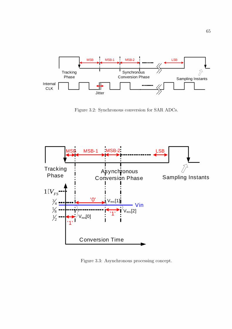
65
MSB MSB-1 LSB
SynchronousConversion Phase
TrackingPhase Sampling Instants
MSB-2
Jitter
Internal CLK
Figure 3.2: Synchronous conversion for SAR ADCs.
MSB MSB-1 MSB-2 LSB
Sampling Instants
TrackingPhase
AsynchronousConversion Phase
Vin
'1'
'0'
'1'
Conversion Time
43
85
21
FSV⋅1
Vres[0]
Vres[1]
Vres[2]
Figure 3.3: Asynchronous processing concept.

66
3.2.2 Asynchronous Processing
The conventional implementation of the SA algorithm, such as an SAR converter,
relies on a synchronous clock to divide the time into a signal tracking phase and
conversion phase which progresses from the MSB to the LSB as shown in Fig. 3.2. For
an N -bit converter with conversion rate of Fs, a synchronous approach would require
a clock running at least (N + 1) · Fs. Since a SAR converter is traditionally used in
lower conversion rate regime, therefore, clock generation is less of an issue. However,
for a high-speed converter, the clock generation of this high-speed internal clock is
a significant overhead. For example, a 300 MS/s and 6-bit SAR would require a 2.1
GHz clock. Synthesizing such a high-frequency clock plus clock distribution network
would likely consume more power than the ADC itself. From speed perspective,
every clock cycle has to tolerate the worst case comparison time, which is composed
of maximum DAC settling time and comparator resolving time depending on the
minimum resolvable input level. In addition, every clock cycle requires margin for
the clock jitter which will either slow down the conversion speed or impose a stringent
jitter requirement on the clock generator.
Therefore, the power and speed limitations of a synchronous SA design comes
largely from the high-speed internal clock. By using asynchronous processing of the
internal comparisons, it removes the need for such a clock and substantially improves
the power efficiency compared to a synchronous design. On the top level, a global
clock running at the sample rate is still used for an uniform sampling, since most

67
of the digital baseband to date remains in a synchronous world. The concept of
asynchronous processing is to trigger the internal comparison from MSB to LSB like
dominoes. Shown in Fig. 3.3, whenever the current comparison is complete, a ready
signal is generated to trigger the following comparison.
The voltage difference (Vres) between input signal and reference level determines
the comparator resolving time. For example, a typical regenerative latch has the
following tradeoff between input voltage (Vres) and resolving time (Tcmp) [35].
Tcmp =τ
Ao − 1· ln VFS
Vres
= K · ln VFS
Vres
(3.1)
where Ao is the small-signal gain of the internal inverting amplifier, τ is the time
constant at the latch outputs and VFS is the full logic swing level.
Depending on the comparator topology, the resolving time and input voltage
tradeoff will change. Nevertheless, this simple regenerative latch model provides in-
tuition into how asynchronous processing helps to improve the conversion speed. For
an N-bit converter, the total comparison time of both synchronous and asynchronous
design can be expressed as,
Tasync =N−1∑i=0
K · ln VFS
Vres[i]
Tsync = N ·K · ln VFS
Vmin
(3.2)
where Vres[i] denotes the input voltage of the comparator at ith stage (Fig. 3.3), and

68
0
FSV⋅2/1
FSV⋅− 2/1
Vres[0] Vres[1] V res[2] Vres[3]FSV⋅− 6/1
Figure 3.4: Best (solid line) and worst (dash line) case of Vres profile
Vmin is usually set by the LSB level.
Clearly, the asynchronous conversion takes the advantage of the faster comparison
cycles, since only one of these Vres[i],∀i ∈ [0, N − 1] will fall within ±1/2 LSB due
to the successive approximation algorithm. The amount of conversion time savings
between Tasync and Tsync is a function of the number of bits as well as the profile
of Vres[i], which depends on the input voltage level. In the extreme case, a 1-bit
converter does not benefit from asynchronous processing, since the only comparison
cycle is always limited by the worst-case resolving time. As the number of bits
increase, Vres[i] will distribute over the full scale range and thus create time savings.
Intuitively, the wider the range of Vres, the faster conversion speed it can achieve.
With the assistance of numerical analysis of Eq. (3.2), the best case scenario is found

69
when input signal is at full swing, i.e. Vres reaches ±1/2VFS. When Vres alternates
its polarity from consecutive comparison cycles, it results in the longest conversion
time, as shown in Fig. 3.4.
The ratio of Tasync
Tsyncof both cases is derived as a function of number of bits in
order to explore the theoretical performance bound of asynchronous processing. In
the best case, Vres[i] are simply VFS/2, VFS/4, VFS/8, ... ,VFS/2N , assuming a binary
successive approximation algorithm. If VLSB = VFS/2N , the ratio of Tasync
Tsynccan be
expressed as,
Tasync
Tsync
=ln VFS
VLSB+ ln VFS
2VLSB+ ln VFS
4VLSB+ · · · ln VFS
2N−1VLSB
N · ln VFS
VLSB/2
=N2 ln 2− N
2(N − 1) ln 2
N(N + 1) ln 2=
1
2(3.3)
In the worst case, the input voltage level that leads to comparison results with
alternating polarity can be better understood as the number of bits increases from
2-bit case, assuming Vres begins from positive side.

70
2-bit Case ⇒ Vres[0]− VFS
4< 0
3-bit Case ⇒ Vres[0]− VFS
4+
VFS
8> 0
4-bit Case ⇒ Vres[0]− VFS
4+
VFS
8− VFS
16< 0
...
⇒ 1
8(1 +
1
4+
1
16+ · · · ) < Vres[0] <
1
4(1− 1
4− 1
16+ · · · )
⇒ Vres[0] → 1
6VFS (3.4)
Given the derived results from Eq. (3.4), the worst case conversion time occurs
when Vin is equal to VFS
3or 2VFS
3, and the ratio of Tasync
Tsyncis thus derived as follows,
Tasync
Tsync
=ln VFS
1/6·VFS+ ln VFS
1/12·VFS+ · · · ln VFS
max(1/(3·2N )·VFS ,VLSB/2)
N · ln VFS
VLSB/2
=(N − 1) ln 3 + ln 2 + N
2(N + 1) ln 2
N(N + 1) ln 2(3.5)
Note that the ratio of Tasync
Tsyncin Eq. (3.5) approaches 1/2 as N increases. In
conclusion, given the lower and upper bound from Eq. (3.3) and (3.5), the maximum
resolving time reduction between synchronous and asynchronous case is two fold.
Moreover, the conversion time savings over a synchronous approach increases with
higher ADC resolution.

71
ADC1
ADC2
2-PhCLK
Clk0
Clk1
Ready Generator
SRLatch
Non-BinaryCapacitorNetwork
SwitchLogic
& Bit
Caches
Pulse Generator
Sequencer(Multi-Phase CLK )
iCLK0
iCLK6
bit0
bit6
SRAM
Vin
Vref+
Vref -
Figure 3.5: Simplified block diagrams of the ADC architecture.
3.2.3 Architecture
While there are several possible architectures to incorporate the asynchronous
processing concept, the first prototype has utilized only one comparator with a charge
redistribution network to achieve a low complexity implementation similar to an SAR
converter. Since the internal comparisons use the same comparator, it does not require
special attention to reduce its offset in the analog domain as the global offset can be
subtracted in the digital domain. However, the overall conversion speed is slowed
down because the comparator must be reset after each comparison cycle. The charge
redistribution capacitor network is used to sample the input signal and serves as a
digital-to-analog converter (DAC) for creating and subtracting reference voltages.
Besides asynchronous processing, time interleaving [36] is used to increase the

72
maximum conversion rate over what a single ADC can achieve. Note that there are
power and area overheads as the number of parallel converters increases. Therefore,
a single asynchronous ADC should be optimized for high speed and small silicon
area. In this prototype (Fig. 3.5), two ADCs are time interleaved for a doubling of
the sample rate over an individual ADC. The two phase (0 and 180 degree) clocks
are provided via on-chip inversion, and used as sampling clocks and reset signals.
The high input bandwidth (>4 GHz) of the individual converter achieved here would
actually allow additional time interleaving.
There are two critical delay paths in this architecture, which involve signal and
timing. For the signal path, each internal comparison result is stored in a SR latch as
a buffering stage to the temporary bit caches. For the asynchronous timing path, the
comparator’s outputs are detected by a ready signal generator as a data completion
flag of each comparison cycle. This ready signal then drives a sequencer to provide
multiple-phase clocks for switching logic and temporary bit caches to store the in-
ternal comparison results. A separate pulse generator creates a reset phase for the
comparator to avoid any memory effect from the previous comparisons. Note that the
ready signal generator, pulse generator, and sequencer are the dedicated digital logic
functions to perform asynchronous conversion and they occupy only a small portion
of the silicon area.
Finally, the bit streams at the output of the bit caches are designed for high
throughput which raises the difficulty of real-time streaming off chip. Therefore, a

73
Vb
VinVip
Qn Qp
φeq
φstrobe φstrobeφ2aφ2aφeq
pre-amplifier regenerative latch
Figure 3.6: Dynamic comparator schematic.
1K-depth on-chip SRAM is used to store the converted data, and later read out to
off-chip in a much slower rate. The integration of the SRAMs is solely for testing
purpose, and occupies the most of the die area.
3.3 Circuit Implementation Details
3.3.1 Dynamic Comparator and Ready Signal
The design of the comparator requires special consideration because of the need to
generate a data ready signal. Shown in Fig. 3.6, a dynamic comparator is used that
is composed of a pre-amplifier and regenerative latch. The complementary outputs
of the comparator are connected to the positive supply during the reset phase and

74
one of the two outputs (Qp and Qn) is pulled down to the negative supply during
comparison. Therefore, digital logic which is able to distinguish state ’1”1’ (reset
phase) from state ’1”0’ or ’0”1’ (data ready) seems to be sufficient for the ready
signal generation. However, one potential issue with asynchronous processing is that
the comparator can be in a metastable state when the input is sufficiently small. The
time needed for the comparator outputs to fully resolve may take arbitrarily long.
As a result, the comparator is designed fast enough such that this only occurs when
the input signal is less than 1 LSB, which means the decision does not effect the
converter accuracy. In this case, the ready signal generator should still set the flag
and the decision result is simply taken from the previous value stored in the SR latch.
To achieve this goal, since both outputs (Qp and Qn) will drop together to a lower
level when the comparator is in metastable state, a simple NAND gate with input
threshold above this level is a key solution to the ready signal generation. As Qp and
Qn are to be in state ’0”0’ once they drop across the threshold, the NAND gate will
set the flag and continue the remaining conversion process.
There are reset switches in both the pre-amplifier and latch stage that help to
reduce the comparator recovery time during the reset phase. An input offset can-
cellation is also utilized for the pre-amplifier stage but is not critical in this ADC
architecture as mentioned earlier. Current mirrors between the two stages are use-
ful to reduce charge kickback [37] from the logic level swing of the latch onto the
input capacitors preceded the pre-amplifier. This is especially important since the

75
input capacitor network is pushed to the minimum possible value as will be described
shortly.
3.3.2 Non-Binary Successive Approximation Review
Instead of a binary successive approximation scheme, this ADC adopts redundancy
to allow dynamic decision errors for faster conversion speed [38]. In other words, the
overlapped search range compensates for wrong decisions made in earlier stages as
long as they are within the error tolerance range. This is similar to the redundancy
often used in a pipeline ADC via reduced residue amplification gain. The equivalent
radix is less than 2 and computed as,
Radix = 2Nbit
Nbit+Nrdn (3.6)
,where Nbit is the target bit resolution, and Nrdn is the redundant bit. In this
prototype, 1 extra redundant bit is used for the target of 6-bit resolution. Therefore,
the equivalent radix is about 1.81.
In terms of implementation, there are two basic approaches as shown in Fig. 3.7.
The geometrically scaled capacitor array makes use of a parallel bank of capacitors
ratioed from 1, α, α2... , αN−1, as shown in Fig. 3.7(a). The advantage of this
approach is the low complexity of the switching logic, since only one capacitor will be
switched at each comparison cycle. The propagation delay and power consumption
through switching logic is expected to be lower. However, in this prototype, the

76
αΝ−1Cu CuαCu
Switch Logic
(a) Geometrically scaled capacitor array.
Cu CuCu
Digital ROM
(b) Unitary capacitor array
Figure 3.7: Conventional implementation of radix creation.

77
ratio α is non-integer which significantly increases layout complexity and matching
difficulty [39] for a full array. On the other hand, an unitary capacitor array (Fig.
3.7(b)) can be used to avoid this non-integer matching issue. The non-binary code
words are stored in a digital ROM. However, the propagation delay through a digital
ROM is much larger compared to the previous case due to the longer logic depth.
Moreover, the total input capacitance of both schemes is on the order of 2N times
unit capacitance. Even for a 6-bit case, the total capacitance can be on the order of
pico-farads with even tens of femto-farads unit capacitance which is set by matching
and parasitic considerations. This causes additional power consumption as well as
the difficulty to maintain a high input bandwidth.
3.3.3 Series Non-Binary Capacitive Ladder
Another approach was therefore taken to create an arbitrary radix, i.e. in effect an
analog ROM. This approach uses a ladder structure of a non-binary capacitor array
which allows a significant reduction in the input capacitance with relaxed matching
and layout requirements.
Shown in Fig. 3.8(a), three different sizes of capacitors ratioed from 1:α:β are
used to build the ladder. The approach is to have the equivalent capacitance at every
internal node be identical, i.e. β · Cu. Therefore, the charge redistribution from one
section to the adjacent one always sees the capacitive divider between α · Cu and
β · Cu. This division ratio will determine the radix of the SA algorithm. Based on

78
Vrefp
Vin
αCu
To comparator
βCuβCu Cu Cu
αCu αCu αCu
Vrefn
Vcm
βCu
C in
MSBLSB
(a) Ideal case without parasitic capacitance.
αCu
βCuβCu Cu Cu
αCu αCu αCu
p1Cu
MSBLSB
p2Cup1Cup2Cu
(b) Inclusion of parasitic capacitance.
Figure 3.8: Series Non-binary Capacitive Ladder.

79
the above observations, the design equations of this ladder is derived as,
β = 1 + α‖β
Radix = 1 + βα
(3.7)
Due to the series connection of the capacitors, the equivalent capacitance is de-
creased which reduces the DAC settling time and the total input capacitance. The
traditional tradeoff between matching property and total input capacitance is re-
moved since it does not depend on reducing the unit capacitance size. The total
input capacitance of the proposed ladder is no longer dependent on the number of
ADC bits, and is calculated as,
Cin = [1 + 2 · (α‖β)] · Cu (3.8)
One potential issue with this ladder structure is the vulnerability to the parasitic
capacitance due to interconnects or the capacitor itself, especially when the capacitor
is implemented as a low-cost metal-oxide-metal (MOM) finger capacitor available in
a standard digital CMOS process instead of a higher quality metal-insulator-metal
(MIM) capacitor. The extra capacitance introduced at the floating nodes can change
the effective radix value if the parasitic capacitance is not negligible to the capacitors
in the ladder. In this prototype, the unit capacitance is set at the minimum possible
value and MOM capacitors have non-negligible fringing capacitances, which necessi-
tates a new design equation including the parasitic capacitance, p1 · Cu and p2 · Cu

80
denoted in Fig. 3.8(b).
β = 1 + α‖β′ + p1
Radix = 1 + β′α
β′ = β + p2
(3.9)
By solving Eq. (3.7) and (3.9), one can show that the new ratios (αmod and βmod)
should be modified according to the following relations with the original ones (αorg
and βorg).
αmod = (1 + p1) · αorg
βmod = (1 + p1)βorg − p2
(3.10)
In this design, a standard capacitor model with conventional EDA extraction tools
were used for estimating the parasitic capacitances and were found to be accurate
enough at this level of ADC resolution. Also, the total input capacitance is pushed
down to ∼90 femto-farads, which is a key to the achieved >4 GHz input bandwidth.
3.3.4 Digital Calibration Scheme
As the systematic error is accounted for in the modified design equation, the ADC
is still vulnerable to the random error, such as capacitor mismatch and parasitic vari-
ation. These random errors can change the effective radix from MSB to LSB bit, and
thus reduce the linearity of the ADC. Similar to the gain error of a residue amplifier

81
in a pipeline ADC, the digital combining weights need correction by estimating the
real gain [40]. In this prototype, a foreground digital calibration scheme is developed
to correct the combining weights and currently implemented off-chip. The approach
was to inject a known input signal to the ADC, and use the converted outputs with
initial combining weights to reconstruct the input signal. By using the reconstructed
signal as the reference for an LMS loop, the combining weights can be adapted to the
real values. Alternatively, the combining weights can be directly calculated through
matrix operation using the orthogonality principle. The reason for using an LMS loop
is to reduce the algorithmic complexity to enable a potential on-chip integration.
Shown in Fig. 3.9(a), a ramp signal that spans over the full swing range is injected
as the known signal. The reconstruction of the reference signal is done through a
best linear curve fitting of the the ADC outputs with initial guess of the combining
weights. Next, the same ADC output code words are fed into an adaptive FIR filter to
converge the real combining weights. The simulation results showed the quantization
error can be improved after calibration using several hundred samples. Alternatively,
a sine wave of a certain frequency and full swing amplitude can be used as the prior
information as illustrated in Fig. 3.9(b). By using a FFT processor, the sine wave
is reconstructed by extracting its amplitude, phase and offset at the fundamental
frequency. A benefit of using a sine wave rather than a ramp is the potentially easier
on-chip implementation with high linearity so that the digital calibration can be
turned into an on-chip self-calibration scheme and extended to higher ADC resolution.

82
ADC
+
_
Best linear curve fitting
Before Calibration After Calibration
(a) Calibration with ramp input.
ADC
FFT
+
_
Get amplitude , phase, offset
Before Calibration After Calibration
(b) Calibration with sine wave input.
Figure 3.9: LMS calibration loop.

83
3.3.5 Variable Duty-Cycled Clock
There are two criteria for the global sampling clock, it needs to have a variable
duty-cycle for testing purposes by allowing the time between tracking and conversion
phases to be varied to explore the ADC performance and it should have very low
jitter if RF sub-sampling is to be used. In fact, the RMS jitter should be on the order
of psec using worst-case case analysis to support the sub-sampling capability.
The clock generation is illustrated in Fig. 3.10 and uses two sinusoidal waves are
generated off-chip with a tunable phase skew in between. The waveforms are then
regenerated on chip and combined with an AND gate. The phase skew determines the
duty cycle of the clock source. Another 180 degree phase-shifted clock is achieved by
simply inverting the two sinusoidal waves and going through the same combination
logic. Special attention was paid in both logic and layout level to ensure the exact 180-
degree phase shift. Any phase imbalance causes extra distortion or requires additional
calibration. Finally, the clock jitter is minimized by careful layout, a dedicated power
domain and a clean clock source with extra bandpass filtering. In addition, the edge
rate of the sampling clock should be high enough to reduce the jitter, which results in
extra power dissipation in the large sized buffers. The jitter due to intrinsic noise of
the logic gates are analyzed and simulated to ensure it is well below the specification.

84
AND
BUF On-chip
Figure 3.10: Variable duty-cycled clock generation.

85
3.3.6 High-Speed Digital Logic
The speed of the entire asynchronous and switching logic is also critical to the
speed of conversion rate. Therefore, all the digital logic in the critical path is custom
dynamic logic and optimized using logical efforts [41] as well as careful layout. The
dynamic logic uses a weak keeper transistor to avoid charge leakage and enhance
noise invulnerability. Moreover, the dynamic registers are designed for minimal clock
loading as these are driven by the asynchronous logic. Note that the pulse duration
is adjusted by a variable MOS resistor operated deep in the triode region in order to
explore the tradeoff between conversion speed and dynamic error. The less critical
digital blocks such as bit caches, and SRAM controller are made from standard cells
provided by the foundry to save the design time. Nevertheless, the timing constraint
between ADC and testing SRAM is very tight, which requires careful design of the
interface circuitry.
3.4 Measured Results
The prototype ADC was fabricated in a 1.2 V 0.13 µm six-metal one-poly digital
CMOS process. Chip on board packaging was used on two versions of PCB designs
to measure ADC performance below and above Nyquist frequency (above Nyquist to
investigate the use of sub-sampling). Fig. 3.12 shows the Nyquist testing board. A
photomicrograph is shown in Fig. 3.11. The total chip size measures 1.7x1.4 mm2,

86
Figure 3.11: DNL and INL before and after combining weights calibration.
while each ADC occupies only 250x240 µm2 which reduces the overhead of time
interleaving.
The static performance is characterized through DNL and INL measurement.
Shown in Fig. 3.13, DNL and INL improves from over 1 LSB to within half LSB
after combining weights calibration described in section 3.3.4. It is equivalent to 2 dB
SNDR improvement, which implies the random error at 6 bit level is not significant.
The dynamic performance measurements (Fig. 3.14(a)) show that the ENOB of a
single ADC scales from 5.3 bit at 300 MS/s to 3.7 bit at 500 MS/s, demonstrating
the straight-forward tradeoff between ENOB and conversion rate which is inherent to
the proposed ADC architecture. In Fig. 3.14(b), the dynamic performance is further

87
Figure 3.12: PCB for testing Nyquist frequencies.

88
10 20 30 40 50 60-1.5
-1
-0.5
0
0.5
1
1.5DNL
code
LSB
10 20 30 40 50 60-1.5
-1
-0.5
0
0.5
1
1.5INL
code
LSB
10 20 30 40 50 60-1.5
-1
-0.5
0
0.5
1
1.5DNL
code
LSB
10 20 30 40 50 60-1.5
-1
-0.5
0
0.5
1
1.5INL
codeLS
B
Before Calibration
After Calibration
Figure 3.13: DNL and INL before and after combining weights calibration.
explored using RF input above Nyquist ranging from 3 to 5 GHz, showing that the
SNDR remains above 30dB even with an input frequency over 4 GHz.
Fig. 3.15 shows the performance of time interleaving two of the ADCs to achieve
600 MS/s sampling rate at twice the power and area. Off-chip digital subtraction
of each ADC offset removes spurious tones improving the SNDR by 0.7 dB. Note
that there is little reduction of SNDR at lower frequency, but as the input frequency
increases above 300 MHz, the clock skew between paths yields a several dB SNDR
reduction. To prove this, the clock skew is extracted through Hilbert transformer
and then compensated by digital interpolation. The results (Fig. 3.16) show that
SFDR improves 11 dB and SNDR improves 2 dB. The total power consumption
excluding SRAM and IO pads consumes 5.3 mW while analog, digital and clock

89
(a)
(b)
Figure 3.14: Measured SNDR versus fs and fin for single ADC (a) below and (b)above Nyquist frequency.

90
(a)
0 50 100 150 200 250 300-80
-60
-40
-20
0
MHz
Mag
nit
ud
e (d
B)
Fs = 600MS/sFin = 159MHzAin = -0.42dBSNDR = 33.14dB
(b)
Figure 3.15: (a) Measured SNDR versus fs and fin for time-interleaved ADC and its(b) FFT spectrum measured at 159 MHz input.
91
0 50 100 150 200 250 300-80
-70
-60
-50
-40
-30
-20
-10
0
dB
MHz
Before Phase Calibration
0 50 100 150 200 250 300-80
-70
-60
-50
-40
-30
-20
-10
0
MHz
dB
After Phase Calibration
SFDR=35dBSNDR=30.1dB
SFDR=46dBSNDR=32.2dB
Figure 3.16: FFT spectrum before and after clock skew calibration.
section consuming 1.2 mW, 3.2 mW and 0.9 mW, respectively. The performance of
the chip is summarized in Table 3.1.
3.5 Applicability
3.5.1 Technology Scaling
As a medium resolution ADC is not limited by KT/C noise, it generally benefits
from technology scaling. This also applies to the proposed asynchronous ADC archi-
tecture, since most circuits are open-loop and digitally operated while only limited by
capacitor matching accuracy. A first-order power and speed analysis for technology
scaling is explored assuming a constant field scaling, i.e. dimension of transistors and
supply voltage scales down by 1/S. The conversion time is mainly dominated by
the signal tracking time, comparator speed and digital propagation delay. The value

92
Table 3.1: Performance Summary (25 ◦C)
Technology 0.13-µm 6M1P Digital CMOS
Package Chip on board
Resolution 6 bit
Sampling Rate 300-500 MS/s for singleADC (600 MS/s-1 GS/s fortime-interleaved one)
Supply Voltage 1.2 V
Input 3dB Bandwidth >4 GHz
Peak SNDR 34 dB at 600 MS/s
FOM 0.22 pJ/conversion step
Power
Analog 1.2 mW
Total Power: 5.3 mWDigital 3.2 mW
Clock 0.9 mW
of the capacitor array is assumed fixed to preserve the matching property, and the
on-resistance of a MOS switch is deliberately scaled down by fixing W. Therefore,
the tracking time constant (RonCs), comparator bandwidth (∝ fT of a transistor),
and digital gate delay (CV/I) all scale down by 1/S with the consideration of ve-
locity saturation. From power perspective, if the overdrive voltage and W/L are
assumed fixed, the analog power scales with supply voltage. The digital switching
power (fCV 2) scales down by 1/S2 [42], while that of clock network scales less due to
the relatively larger sized sampling switch. Table 3.2 summarized the scaling trend,
which predicts the figure-of-merit (FOM) defined in Eq. (3.11) improves at least
1/S2.

93
Table 3.2: Technology Scaling on the proposed ADC architecture
Ttrack Tcomp Tdig
RC ∼ 1/S 1/fT ∼ 1/S RC ∼ 1/S
Panalog Pclk Pdig
IV ∼ 1/S fCV 2 ∼ [1/S − 1/S2] fCV 2 ∼ 1/S2
FOM =Power
2ENOB · fs
(3.11)
3.5.2 Future Role of the Proposed ADC Topology
Fig. 3.17 shows a common usage of ADC topologies in terms of resolution and
sampling rate. Traditionally, flash-type ADCs, including sub-ranging and folding
converters, dominate over the high-speed and medium-resolution regime, while con-
suming redundant power. To save the extra power consumption, an SAR converter
can be a better solution, however, it is normally used for high to medium resolution
while limited to speeds of 10s’ MHz to KHz range. By using asynchronous process-
ing technique presented in this silicon prototype, it has successfully pushed the SA
algorithm implementation to the speed of 100s’ MHz. The proposed architecture can
be easily extended to higher ADC resolution before being limited by KT/C noise.
In fact, the FOM improves as the ADC bits increases, since the speed scale down
proportionally while quantization levels (2ENOB) scales up exponentially. Finally,
greater than 4 GHz input bandwidth renders the potential to time-interleave close to
10 GHz for supporting Nyquist rate sampling.

94
1k 10k 100k 1M 10M 100M 1G 10G
Sampling Rate
468
1012141618
2022
24
AD
C R
eso
lutio
n
2
Pipeline
Flash
SAR
Sigma-Delta
Async. TimeInterleave
Figure 3.17: Future role of the SA architecture.

95
Figure 3.18: FOM comparisons with recent >10 MHz, 6-8 bit ADCs from ISSCC00-05.
3.6 Conclusion
An asynchronous ADC architecture has been demonstrated to achieve a high
power efficiency for a high-speed and medium resolution converter. While the asyn-
chronous processing concept can be incorporated with other ADC topologies, the first
prototype has been realized with a SA architecture to achieve FOM of 0.22pJ/conversion
step in 0.13-µm CMOS process. The results have been compared with the recent 6-8
bit, high-speed (>10MS/s) ADCs in ISSCC 2000-2005, as shown in Fig. 3.18. The
FOM of the proposed architecture is anticipated to further improve with continued

96
technology scaling.
97
Chapter 4
Conclusion and Future Work
This research work has proposed both system and circuit solutions to minimize the
overall cost of implementing an ultra-wideband radio. It is found that combining the
different disciplinary domains including communication theories, signal processing al-
gorithm and analog/digital IC design is truly the key to better solutions. Especially,
the silicon implementation of most modern communication systems has reached the
point of full system-on-chip (SOC) solutions for lower cost. With this level of integra-
tion and tighter power constraint, the boundary between system and circuit, analog
and digital becomes even more obscure.
Looking into the future, the results derived from this thesis work can drive into
several directions. First of all, the sub-sampling front-end is a promising architec-
ture for any wideband system, besides UWB. Especially, the future wireless radio
front-end are going wider bandwidth to utilize more unlicensed bands and multiple

98
standards. The performance degradation and anti-aliasing filtering requirements are
greatly reduced, due to the lower in-band SNR and under-sampling ratio. From tech-
nology scaling perspective, the increasing intrinsic frequency of a transistor will favor
the implementation of a sub-sampling front-end, where more circuit blocks will be op-
erated in the RF band while reducing the overall complexity. The emerging MEMS
filter technology should also be paid attentions as it is a promising candidate for more
attenuations for out-of-band aliasing.
Secondly, the analytic signal processing can be further explored for UWB radio.
The example derived in this thesis is assuming there is no inter-symbol interference
(ISI) between pulses. However, for higher pulse repetition rate, an equalizer incor-
porating analytic signal transformation can be used to remove the interference with
minimal overhead of computation complexity. Additionally, the analytic signal pro-
cessing can be extended for a tracking application using impulse radio approach, since
the trajectory of an analytic matched filter serves as the signature of a certain pulse
waveform.
Finally, the wideband radio has driven the demand of high-speed ADCs with very
low power consumption for portable device applications. The high sampling cost
has long been the bottleneck of such systems, which often necessitates more analog
processing. Recently, there has been a new revolutionary wave of pushing the power
efficiency of ADCs, which has entered below 1 pJ/conversion step regime. The greatly
reduced sampling cost will enable new system architecture where more digital signal

99
processing can be implemented. The asynchronous ADC architecture has demon-
strated a superior power efficiency and possess a great potential to scale for higher
sampling speed, more resolution, and future technology. The asynchronous concept
and circuit techniques introduced in this research work can be crucial for pushing the
performance of future high-speed and medium-resolution ADCs, achieving below 0.1
pJ/conversion step power efficiency.

100
Bibliography
[1] “Revision of part 15 of the commission’s rule regarding ultra-wideband transmis-
sion systems,” Federal Communications Commission, First Report and Order,
Feb. 2002.
[2] S. Roy, J. R. Foerster, V. S. Somayazulu, and D. G. Leeper, “Ultrawideband radio
design: The promise of high-speed, short-range wireless connectivity,” Proceed-
ings of the IEEE, vol. 4 Issue 2, pp. 295–311, Feb. 2004.
[3] G. R. Aiello and G. D. Rogerson, “Ultra-wideband wireless systems,” IEEE
Microwave Magazine, vol. 4 Issue 2, pp. 36–47, June 2003.
[4] J. Bergervoet et al., “An interference robust receive chain for UWB radio in
SiGe BiCMOS,” IEEE International Solid-State Circuits Conference (ISSCC)
Dig. Tech. Papers, vol. 48, pp. 200–201, Feb. 2005.
[5] A. Ismail and A. Abidi, “A 3.1 to 8.2GHz direct conversion receiver for
MB-OFDM UWB communications,” IEEE International Solid-State Circuits
Conference (ISSCC) Dig. Tech. Papers, vol. 48, pp. 208–209, Feb. 2005.

101
[6] B. Razavi et al., “A 0.13µm CMOS UWB transceiver,” IEEE International
Solid-State Circuits Conference (ISSCC) Dig. Tech. Papers, vol. 48, pp. 216–
217, Feb. 2005.
[7] A. Tanaka et al., “A 1.1v 3.1-to-9.5GHz MB-OFDM UWB transceiver in 90nm
CMOS,” IEEE International Solid-State Circuits Conference (ISSCC) Dig. Tech.
Papers, vol. 49, pp. 120–121, Feb. 2006.
[8] C. Sandner et al., “A WidMedia/MBOA-Compliant CMOS RF transceiver for
UWB,” IEEE International Solid-State Circuits Conference (ISSCC) Dig. Tech.
Papers, vol. 49, pp. 122–123, Feb. 2006.
[9] WiMedia Alliance. [Online]. Available: http://wimedia.org/
[10] R. A. Scholtz, “Multiple access with time-hopping impulse modulatoin,” Proc.
MILCOM, vol. 2, pp. 447–450, Oct. 1993.
[11] I. O’Donnell, M. Chen, S. Wang, and R. Brodersen, “An integrated, low power,
ultra-wideband transceiver architecture for low-rate, indoor wireless systems,”
IEEE CAS Workshop on Wireless Communications and Networking, Sept. 2002.
[12] M. S. W. Chen and R. W. Brodersen, “A subsampling UWB radio architecture
by analytic signalling,” Proc. ICASSP, vol. 4, pp. 533–536, May 2004.
[13] ——, “A 6b 600MS/s 5.3mw asynchronous ADC in 0.13µm CMOS,” IEEE In-

102
ternational Solid-State Circuits Conference (ISSCC) Dig. Tech. Papers, vol. 49,
pp. 574–575, Feb. 2006.
[14] S. Lida et al., “A 3.1 to 5GHz CMOS DSSS UWB transceiver for WPANs,”
IEEE International Solid-State Circuits Conference (ISSCC) Dig. Tech. Papers,
vol. 48, pp. 214–215, Feb. 2005.
[15] A. Aggarwal et al., “A low power implementation for the transmit path of a
UWB transceiver,” Proc. IEEE Custom Integrated Circuits Conference (CICC),
Sep. 2005.
[16] J. G. Proakis, Digital Communications. New York: McGraw Hill, 1995.
[17] R. G. Vaughan, N. L. Scott, and D. R. White, “The theory of bandpass sam-
pling,” IEEE Transactions on Signal Processing, vol. 39 No. 9, pp. 1973–1984,
Sept. 1991.
[18] M. Shinagawa, Y. Akazawa, and T. Wakimoto, “Jitter analysis of high-speed
sampling systems,” IEEE J. Solid-State Circuits, vol. 25 No. 1, pp. 220–224,
Feb. 1990.
[19] M. S. W. Chen and R. W. Brodersen, “The impact of a wideband channel on
UWB system design,” Proc. MILCOM, vol. 1, pp. 163–168, Nov. 2004.
[20] A. Oppenheim and R. Schafer, Discrete-Time Signal Processing 2nd Ed. En-
glewood Cliffs, NJ: Prentice Hall, 1998.

103
[21] H. Schantz, “Bottom fed planar elliptical UWB antennas,” IEEE Conference on
Ultra Wideband Systems and Technologies, pp. 219–223, Nov. 2003.
[22] S. Ghassemzadeh, R. Jana, C. Rice, W. Turin, and V. Tarokh, “Measurement
and modeling of an ultra-wide bandwidth indoor channel,” IEEE Trans. on Com-
munications, vol. 52 No. 10, pp. 1786–1796, Oct. 2004.
[23] D. Cassioli, M. Win, and A. Molisch, “The ultra-wide bandwidth indoor chan-
nel: From statistical model to simulations,” IEEE Journal on Selected Areas in
Communications, vol. 20 No. 6, pp. 1247–1257, Aug. 2002.
[24] M. S. W. Chen, “Ultra wideband baseband design and implementation,” Master’s
thesis, University of California, Berkeley, 2002.
[25] C. Chang, K. Kuusilinna, B. Richards, A. Chen, N. Chan, and R. Brodersen,
“Rapid design and analysis of communication systems using the BEE hardware
emulation environment,” Proc. IEEE Rapid System Prototyping Workshop, pp.
148–154, June 2003.
[26] C. Shi and R. Brodersen, “Automated fixed-point data-type optimization tool
for signal processing and communication,” Proc. Design Automation Conference,
pp. 478–483, June 2004.
[27] G. Chien and P. R. Gray, “A 900-MHz local oscillator using a DLL-based fre-

104
quency multiplier technique for PCS applications,” IEEE Journal of Solid-State
Circuits, vol. 35 No. 12, pp. 1996–1999, Dec. 2000.
[28] P. Scholtens and M. Vertregt, “A 6b 1.6 Gsample/s flash ADC in 0.18 µm CMOS
using averaging termination,” IEEE International Solid-State Circuits Confer-
ence (ISSCC) Dig. Tech. Papers, vol. 1, pp. 168–457, Feb. 2002.
[29] X. Jiang, Z. Wang, and F. Chang, “A 2GS/s 6b ADC in 0.18µm CMOS,” IEEE
International Solid-State Circuits Conference (ISSCC) Dig. Tech. Papers, vol. 1,
pp. 322–497, Feb. 2003.
[30] R. Taft et al., “A 1.8v 1.6GS/s 8b self-calibrating folding ADC with 7.26
ENOB at Nyquist frequency,” IEEE International Solid-State Circuits Confer-
ence (ISSCC) Dig. Tech. Papers, vol. 1, pp. 252–256, Feb. 2004.
[31] P. Figueiredo et al., “A 90nm CMOS 1.2V 6b 1GS/s two-step subranging
ADC,” IEEE International Solid-State Circuits Conference (ISSCC) Dig. Tech.
Papers, vol. 49, pp. 568–569, Feb. 2006.
[32] G. Van der Plas, S. Decoutere, and S. Donnay, “A 0.16pj/conversion-step 2.5mw
1.25GS/s 4b ADC in a 90nm digital CMOS process,” IEEE International Solid-
State Circuits Conference (ISSCC) Dig. Tech. Papers, vol. 49, pp. 566–567, Feb.
2006.
[33] D. Draxelmayr, “A 6b 600MHz 10mw ADC arrary in digital 90nm CMOS,”

105
IEEE International Solid-State Circuits Conference (ISSCC) Dig. Tech. Papers,
vol. 1, pp. 264–527, Feb. 2004.
[34] B. Murmann and B. Boser, “A 12-bit 75-MS/s pipelined ADC using open-loop
residue amplification,” IEEE J. Solid-State Circuits, vol. 38 No. 12, pp. 2040–
2050, Dec. 2003.
[35] H. J. M. Veendrick, “The behavior of flip-flops used as synchronizers and predic-
tion of their failure rate,” IEEE J. Solid-State Circuits, vol. SC-15, pp. 169–176,
April 1980.
[36] W. Black and D. Hodges, “Time interleaved converter arrays,” IEEE J. Solid-
State Circuits, vol. 15 No. 6, pp. 1022–1029, Dec. 1980.
[37] K. Bult and A. Buchwald, “An embedded 240-mW 10-b 50 MS/s CMOS ADC
in 1-mm2,” IEEE J. Solid-State Circuits, vol. 32, pp. 1887–1895, Dec. 1997.
[38] F. Kuttner, “A 1.2V 10b 20MSample/s non-binary successive approximation
ADC in 0.13µ CMOS,” IEEE International Solid-State Circuits Conference
(ISSCC) Dig. Tech. Papers, vol. 1, pp. 176–177, Feb. 2004.
[39] A. Hastings, The art of analog layout. New Jersey: Prentice Hall, 2001.
[40] A. N. Karanicolas, H. Lee, and K. L. Bacrania, “A 15-b 1-Msample/s digitally
self-calibrated pipeline ADC,” IEEE J. Solid-State Circuits, vol. 28, pp. 1207–
1215, Dec. 1993.

106
[41] I. Sutherland, R. Sproull, and D. Harris, Logical effort: designing fast CMOS
circuits. San Francisco, CA: Morgan Kaufmann, 1999.
[42] J. M. Rabaey et al., Digital integrated circuits: a design perspective. Upper
Saddle River, New Jersey: Pearson Education, 2003.


