EMC DL 20081
Power Integrity and EMC Design for HighPower Integrity and EMC Design for High--speed speed Circuits Packages Circuits Packages
Tzong-Lin Wu, Ph. D.Professor
Department of Electrical EngineeringGraduate Institute of Communication Engineering
National Taiwan UniversityTaipei, Taiwan, ROC
EMC DL 20082
OutlineOutline
• Power Distribution Network (PDN)• Mechanism of Power Noise
• Issues and Quantification of Power Noise
• Solutions of Suppressing Power Noise
– Decoupling Capacitors• Power/ground planes (PKG, PCB)
• Surface mounted capacitor (PCB, PKG)
• Embedded capacitor (PKG)
• On-chip capacitor (Chip)
– Isolation slots
– EBG structures• Electromagnetic Bandgap (EBG) Power Planes
• Photonic Crystal Power Layer (PCPL)
• Conclusion

EMC DL 20083
Trends for high-performance Electronics
*Source: The International Technology Roadmap for Semiconductor (ITRS), 2007 (http://public.itrs.net)
Low voltage High speed
Year Feature Vdd Chip Freq. Power
2007 68nm 1.1V 4.70GHz 189W
2010 45nm 1.0V 5.88GHz 198W
2013 32nm 0.9V 7.34GHz 198W
2016 22nm 0.8V 9.18GHz 198W
2019 16nm 0.7V 11.48GHz 198W

EMC DL 20084 EMC DL 20084
Power Distribution Network (PDN)Power Distribution Network (PDN)
An Electronic SystemAn Electronic System
Ground
Power
Decoupling capacitor on PCB
Decoupling capacitor on Package
Chip Ball Bonding
Flip chipChip
Wire bonding
VRM
EMC DL 20085 EMC DL 20085 5
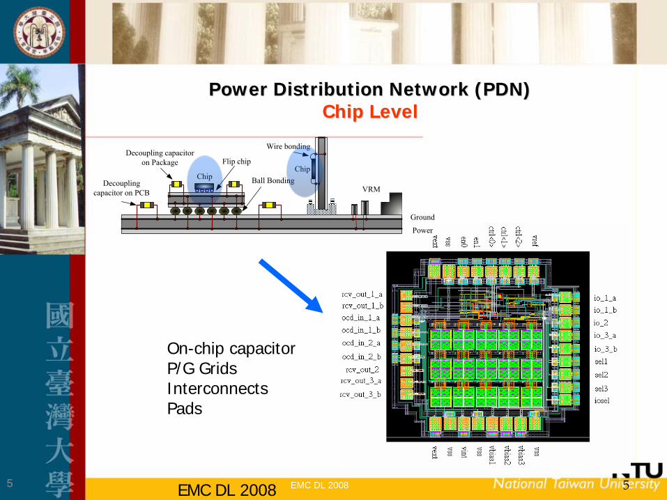
Power Distribution Network (PDN)Power Distribution Network (PDN)Chip LevelChip Level
Ground
Power
Decoupling capacitor on PCB
Decoupling capacitor on Package
Chip Ball Bonding
Flip chipChip
Wire bonding
VRM
On-chip capacitorP/G GridsInterconnectsPads

EMC DL 20086
Power Distribution Network (PDN)Power Distribution Network (PDN) interconnects for Chipinterconnects for Chip--PKGPKG--PCBPCB
Ground
Power
Decoupling capacitor on PCB
Decoupling capacitor on Package
Chip Ball Bonding
Flip chipChip
Wire bonding
VRM
Fine pitch: 50-100umLine length: 100-200 mil
Bump pitch: 100–300umBGA Ball pitch: 0.5mm – 1mm
EMC DL 20087
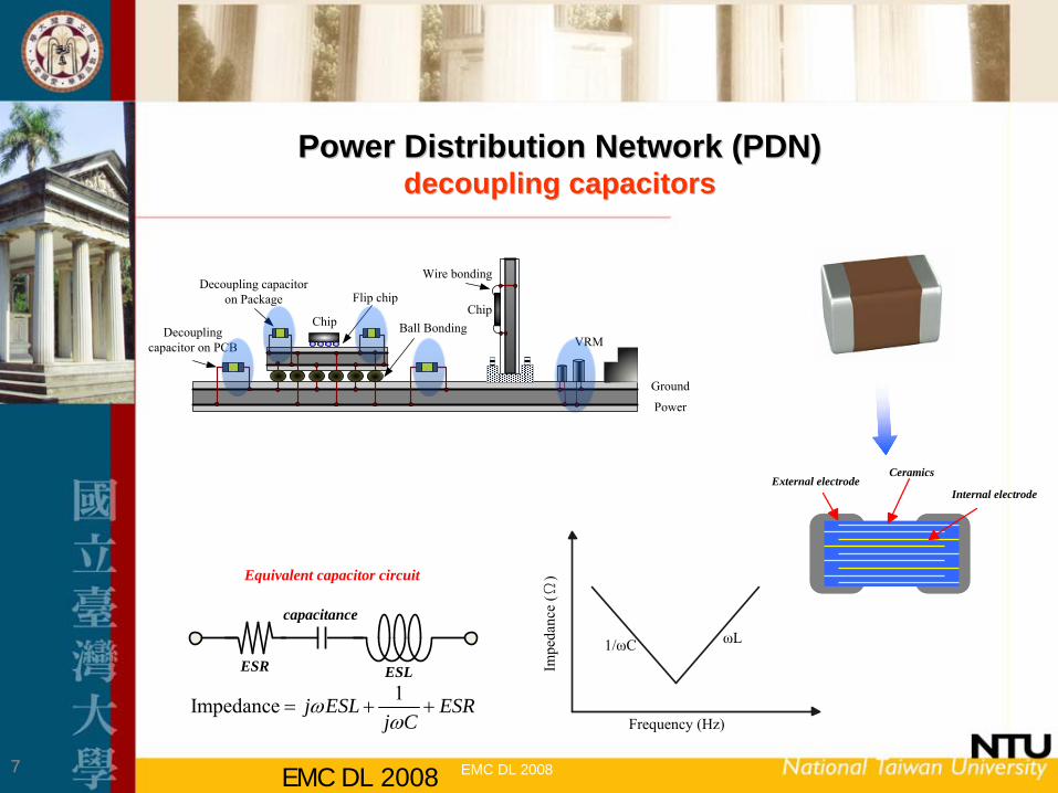
Power Distribution Network (PDN)Power Distribution Network (PDN) decoupling capacitorsdecoupling capacitors
EMC DL 20087
CeramicsExternal electrode
Internal electrode
ESR ESL
capacitance
Equivalent capacitor circuit
1Impedance j ESL ESRj C
ωω
= + +
Impe
danc
e (Ω
)
Frequency (Hz)
1/ωC ωL
Ground
Power
Decoupling capacitor on PCB
Decoupling capacitor on Package
Chip Ball Bonding
Flip chipChip
Wire bonding
VRM
EMC DL 20088
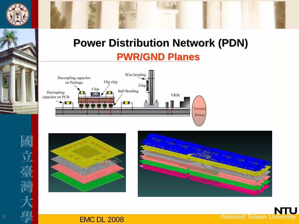
Power Distribution Network (PDN)Power Distribution Network (PDN) PWR/GND PlanesPWR/GND Planes
PowerGND
Ground
Power
Decoupling capacitor on PCB
Decoupling capacitor on Package
Chip Ball Bonding
Flip chipChip
Wire bonding
VRM
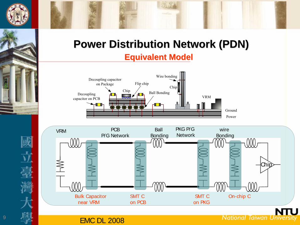
EMC DL 200899
Bulk Capacitornear VRM
SMT C on PCB
SMT C on PKG
On-chip C
PCBP/G Network
PKG P/G Network
Ball Bonding
wire Bonding
Chip
VRM
Ground
Power
Decoupling capacitor on PCB
Decoupling capacitor on Package
Chip Ball Bonding
Flip chipChip
Wire bonding
VRM
Power Distribution Network (PDN)Power Distribution Network (PDN) Equivalent ModelEquivalent Model

EMC DL 200810
Mechanism of the Power Noise : Mechanism of the Power Noise : lowlow--speed viewspeed view
Chipgroud
Frominput stage
LRLC
Outputlead
OUTV
1Q
2Q
LeadVCC
Groundlead
Boardinductance
CCVCHIP
OUTV
OUTI
VGB
+
-
VGB
IcutCIcut
switching voltage
transient currentΔ − I noiseb g
I C dVdtcut L= −1 0
P/G noise arises whenever a changing current flow through the total inductance of the return path
EMC DL 200811
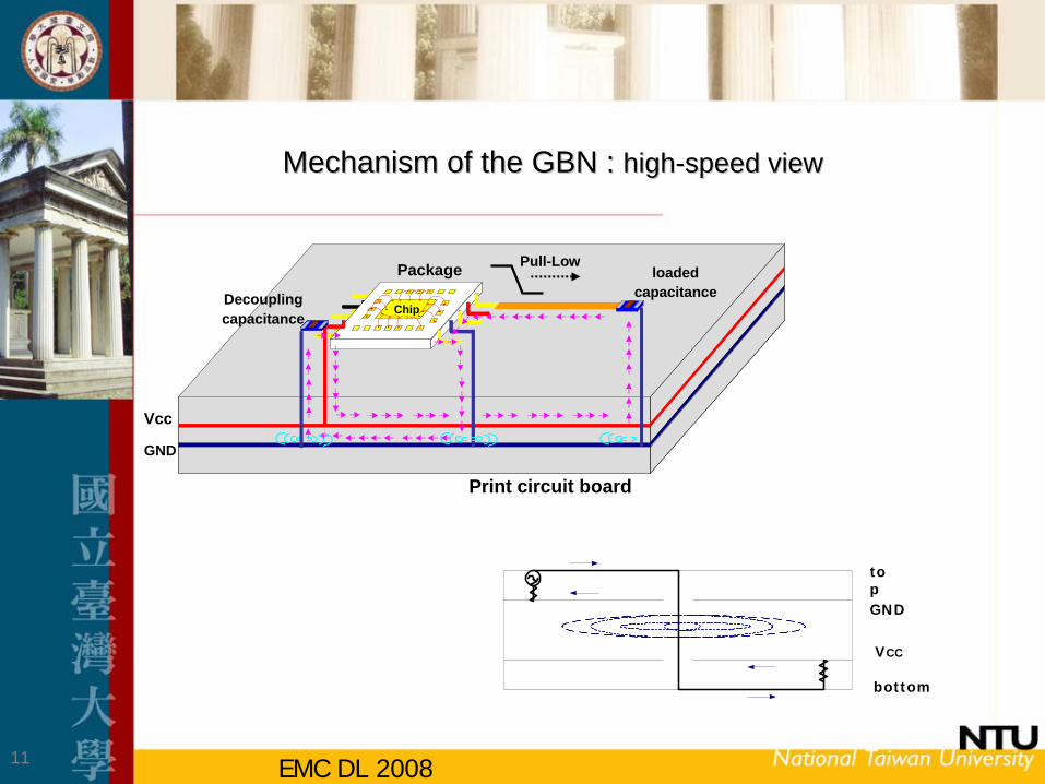
Mechanism of the GBN : Mechanism of the GBN : highhigh--speed viewspeed view
Print circuit board
Package
Vcc
GND
Decouplingcapacitance
loadedcapacitance
Chip
Pull-Low
bottom
to pGND
VCC

EMC DL 200812
Signal in
Via
Layer 1
Layer 2
Layer 3
Layer 4
A 4-layer PCB
EMC DL 200813
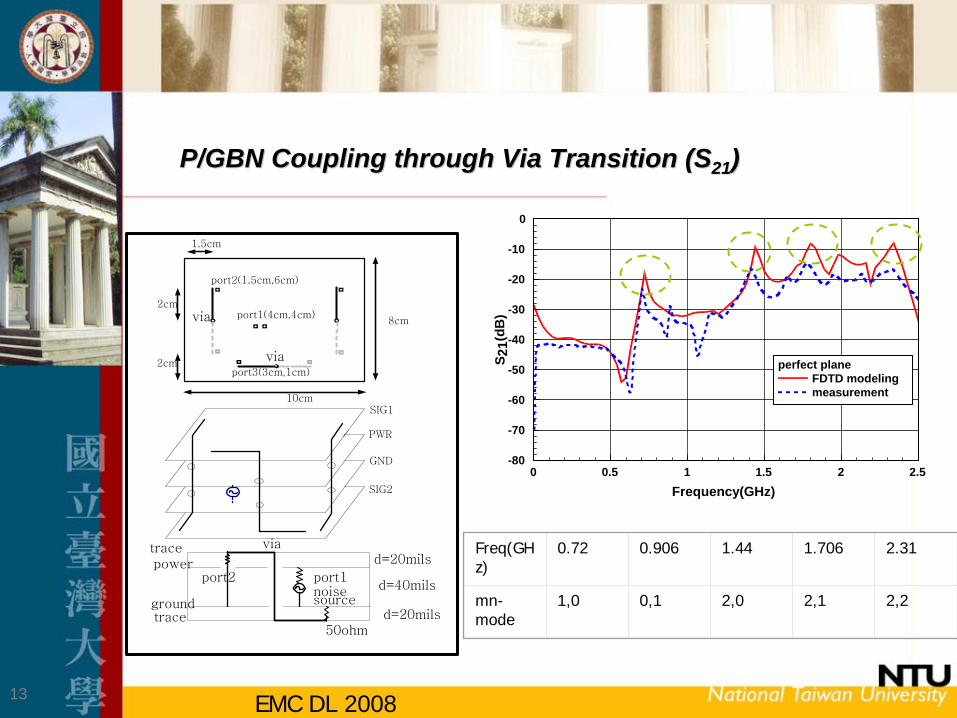
P/GBN Coupling through Via Transition (SP/GBN Coupling through Via Transition (S2121 ))
Freq(GH z)
0.72 0.906 1.44 1.706 2.31
mn- mode
1,0 0,1 2,0 2,1 2,2
10cm
8cm
2cmport1(4cm,4cm)
port2(1.5cm,6cm)
1.5cm
2cm
d=20mils
d=40mils
d=20mils
noisesource
port1
50ohm
port2
viatrace
trace
power
ground
SIG1
PWR
GND
SIG2
via
via
port3(3cm,1cm)
0 0.5 1 1.5 2 2.5Frequency(GHz)
-80
-70
-60
-50
-40
-30
-20
-10
0
S 21(
dB)
perfect planeFDTD modelingmeasurement
EMC DL 200814
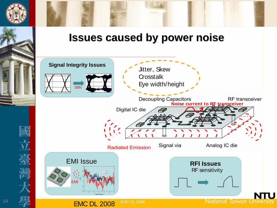
RFI Issues
EMC DL 200814
Issues caused by power noiseIssues caused by power noise
Noise current to RF transceiver
EMI Issue
1 2 3 4 5 6 720
30
40
50
60
70
dBμV
Frequency(GHz)
Case 1 Case 2
20 dBEMI
Signal Integrity Issues
SSN
RF sensitivity
Jitter, SkewCrosstalkEye width/height
EMC DL 200815
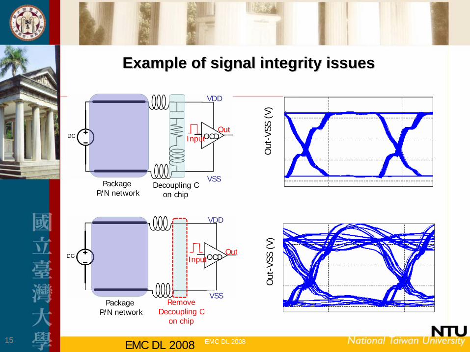
Example of signal integrity issuesExample of signal integrity issues
EMC DL 200815
Decoupling Con chip
Package P/N network
OCDInput
VDD
VSS
Out
InputOut
RemoveDecoupling C
on chip
Package P/N network
VDD
VSS
OCDO
ut-V
SS (
V)O
ut-V
SS (
V)
EMC DL 200816
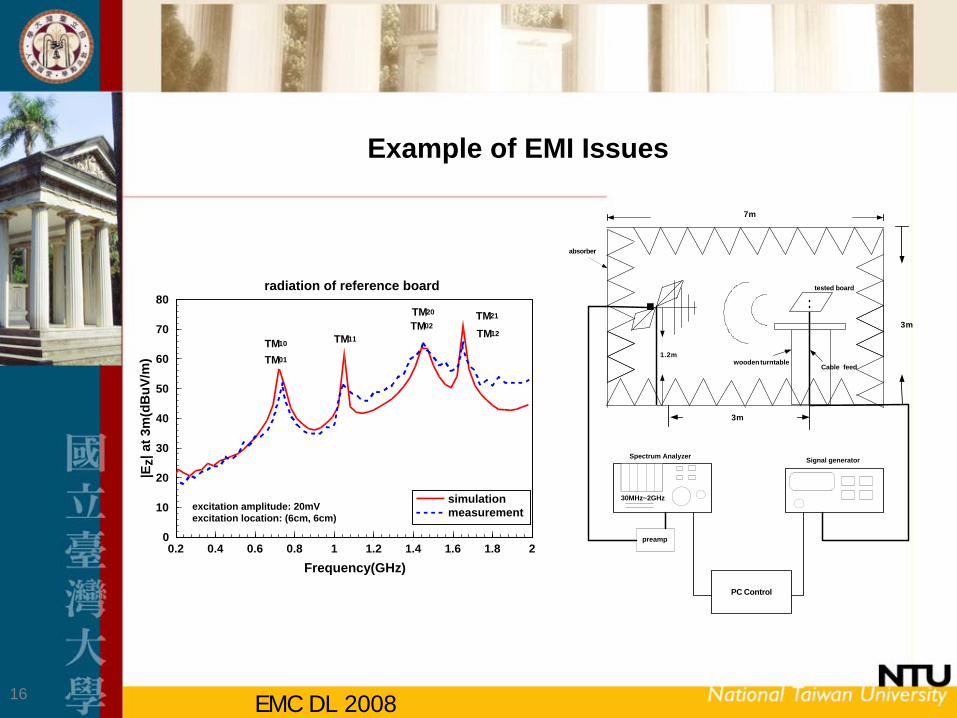
Example of EMI Issues
3m
absorber
Spectrum Analyzer
30MHz~2GHz
Signal generator
preamp
PC Control
wooden turntable
3m
tested board
7m
1.2m
Cable feed
0.2 0.4 0.6 0.8 1 1.2 1.4 1.6 1.8 2Frequency(GHz)
0
10
20
30
40
50
60
70
80
|Ez|
at 3
m(d
BuV
/m)
simulationmeasurement
radiation of reference board
excitation amplitude: 20mV excitation location: (6cm, 6cm)
TM10
TM01
TM11
TM20
TM02TM21
TM12
EMC DL 200817
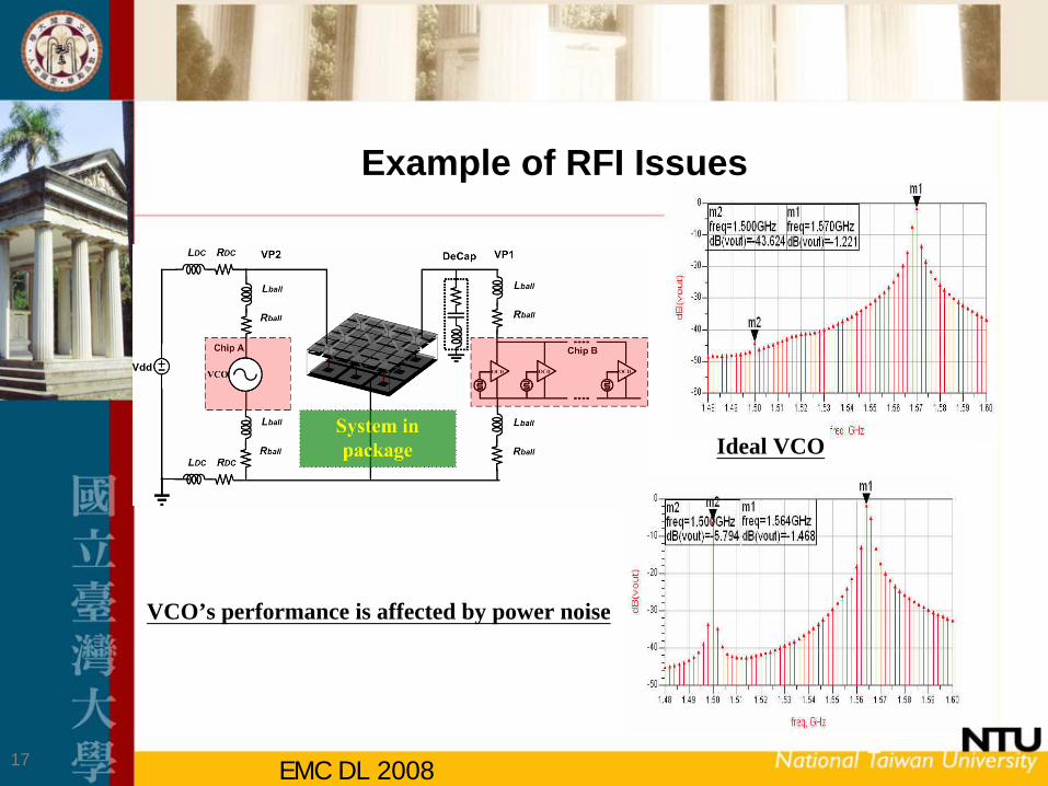
Example of RFI Issues
VCO’s performance is affected by power noise
Ideal VCO
EMC DL 200818
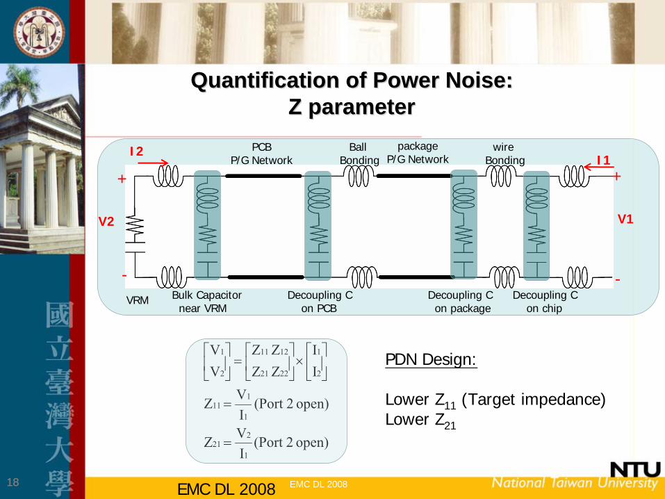
Quantification of Power Noise:Quantification of Power Noise: Z parameterZ parameter
EMC DL 200818
open) 2(Port IVZ
open) 2(Port IVZ
II
ZZ ZZ
VV
1
221
1
111
2
1
2221
1211
2
1
=
=
⎥⎦
⎤⎢⎣
⎡×⎥⎦
⎤⎢⎣
⎡=⎥
⎦
⎤⎢⎣
⎡
Bulk Capacitornear VRM
Decoupling C on PCB
Decoupling C on package
Decoupling C on chip
+
-
V1
+
-
V2
I2I1
PCBP/G Network
packageP/G Network
Ball Bonding
wire Bonding
VRM
PDN Design:
Lower Z11 (Target impedance)Lower Z21

EMC DL 200819
Measurement of PDN ImpedanceMeasurement of PDN Impedance
ZZ--parameter and Sparameter and S--parametersparameters
port1(5cm,4cm)
port2(4cm,8cm)
10cm
10cm
1.6mmX
Y
(0,0)
Floppy drive
HP 8510C
SMA Connector
Coaxial Probes
Transfer impedance
Self impedance: (two probes are very close)
2121 0
11 22 12 21
11 22
12 21 0
21 21
2(1 )(1 )
Assume S 1 (Low impedance PDN)S 0, Z 50
25
SZ ZS S S S
SS
Z S
=− − −
≈ −⋅ = Ω
≈ ⋅
0 2111
212 1Z S
ZS
=− 11 21 2125 (assume 1)Z S S≈ ⋅
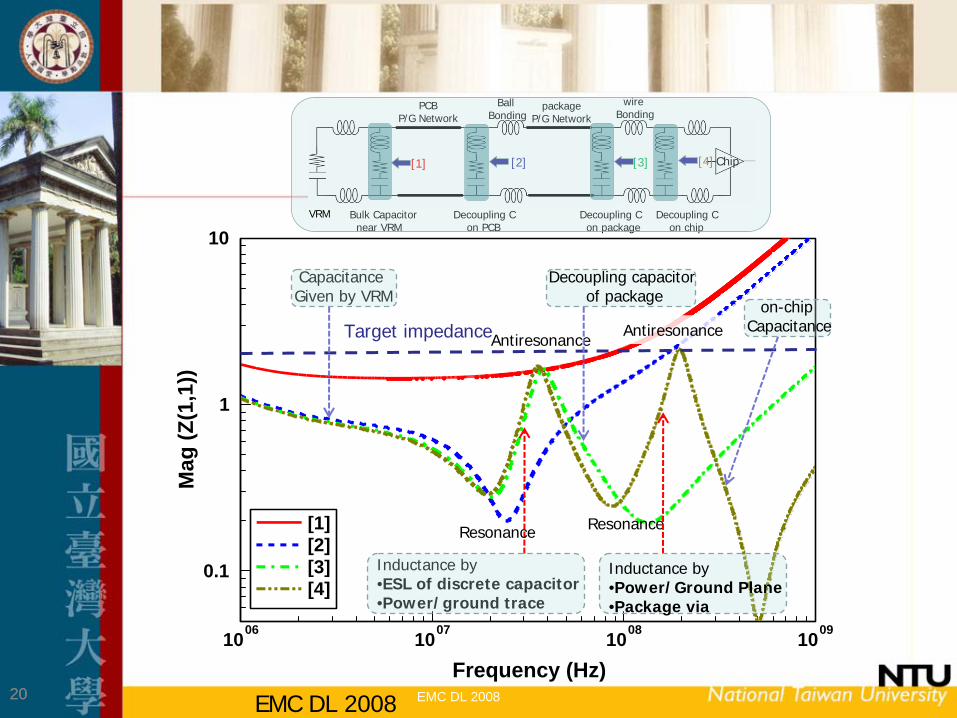
EMC DL 200820 EMC DL 200820
1006 1007 1008 1009
Frequency (Hz)
0.1
1
10
Mag
(Z(1
,1))
[1][2][3][4]
Bulk Capacitornear VRM
Decoupling C on PCB
Decoupling C on package
Decoupling C on chip
PCBP/G Network
packageP/G Network
Ball Bonding
wire Bonding
Chip[1] [2] [3] [4]
Target impedance
Capacitance Given by VRM
Inductance by•ESL of discrete capacitor•Power/ground trace
Resonance Resonance
Antiresonance Antiresonance
Inductance by•Power/Ground Plane•Package via
Decoupling capacitor of package
on-chip Capacitance
VRM
EMC DL 200821
package
Die
PCB
Decoupling capacitor
4cm
4cm
10cm
8cm
port1 port2
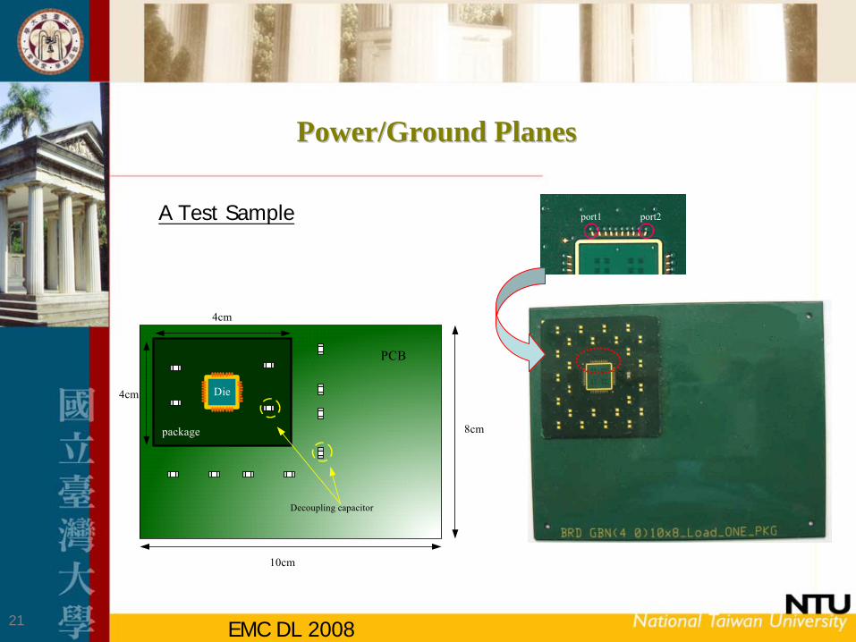
Power/Ground PlanesPower/Ground Planes
A Test Sample

EMC DL 200822
Measurement setup Measurement setup
10 cm
8 cmPCB
package 0.4 mm
probe
VNA
Power ring
Ground ring
Power viaprobe
signalground
Power/Ground PlanesPower/Ground Planes

EMC DL 200823
0 0.5 1 1.5 2 2.5 3 3.5 4 4.5 5frequency(GHz)
-70
-60
-50
-40
-30
-20
-10
0
S21(
dB)
Bare pkgBare PCBpkg+PCB
The SSN could be magnified by the interaction The SSN could be magnified by the interaction of these two cavities and degrades the of these two cavities and degrades the power integrity of the packaged power integrity of the packaged integrated circuitsintegrated circuits.
The PDS behavior of combining the package The PDS behavior of combining the package and PCB is similar to that of considering and PCB is similar to that of considering only the package.only the package.
Power/Ground PlanesPower/Ground Planes Coupling between PKG and PCBCoupling between PKG and PCB
Measurement Results
Sin-Ting Chen, Ting-Kuang Wang, Chi-Wei Tsai, Sung-Moa Wu, James L. Drewniak, Tzong-Lin Wu, “Modeling Noise Coupling Between Package and PCB Power/Ground Planes with an Efficient 2D-FDTD/Lumped Element Method”, IEEE Transaction on Advanced Packaging, Vol. 30, No. 4, pp. 864 –
pp. 871, Nov. 2007.
EMC DL 200824
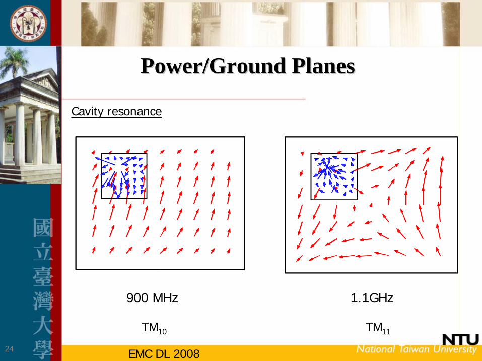
900 MHz 1.1GHz
TM10 TM11
Power/Ground PlanesPower/Ground Planes
Cavity resonance

EMC DL 200825
VRMGround
Power
Bulk capacitor
Decoupling capacitor on PCB
Decoupling capacitor on Package
ChipBall Bonding
SMT CapacitorsSMT Capacitors
Design Question?
• Locations?• Numbers?• Values?
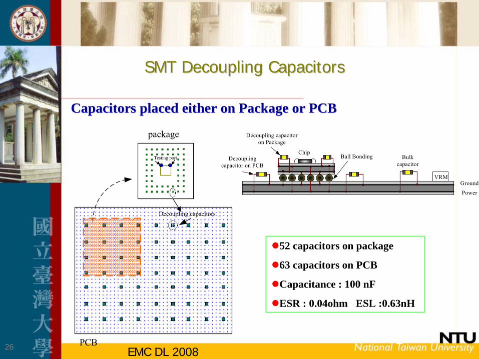
EMC DL 200826
SMT Decoupling CapacitorsSMT Decoupling Capacitors
Capacitors placed either on Package or PCBCapacitors placed either on Package or PCB
PCB
package
Decoupling capacitors
Testing port
52 capacitors on package
63 capacitors on PCB
Capacitance : 100 nF
ESR : 0.04ohm ESL :0.63nH
VRMGround
Power
Bulk capacitor
Decoupling capacitor on PCB
Decoupling capacitor on Package
ChipBall Bonding
EMC DL 200827
0 0.5 1 1.5 2 2.5 3 3.5 4 4.5 5frequency(GHz)
-90
-80
-70
-60
-50
-40
-30
-20
-10
S21(
db)
pkg+PCBpkg+(PCB+cap)(pkg+cap)+PCB(pkg+cap)+(PCB+cap)
The additional resonance peak The additional resonance peak worsens the PDN performance.worsens the PDN performance.
The behavior of the PDN is similar The behavior of the PDN is similar to that with the caps mounted on to that with the caps mounted on the package.the package.
Decoupling capacitors placed on Decoupling capacitors placed on package have better performance.package have better performance.
SMT Decoupling Capacitors for Suppressing the P/GBNSMT Decoupling Capacitors for Suppressing the P/GBN
Capacitors placed either on Package or PCBCapacitors placed either on Package or PCB

EMC DL 200828
C:100nF (on Package)
ESR:0.04ohm
ESL:0.63nH
With increasing the number of decoupling capacitors, the peaks move to higher frequency and their magnitude become smaller.
0 0.2 0.4 0.6 0.8 1 1.2 1.4 1.6 1.8 2frequency(GHz)
-100
-90
-80
-70
-60
-50
-40
-30
-20
-10
S21(
db)
(pkg+PCB)_no cap4 cap8 cap12 cap22 cap52 cap
SMT Decoupling CapacitorsSMT Decoupling Capacitors
Capacitors Number EffectVRM
Ground
Power
Bulk capacitor
Decoupling capacitor on PCB
Decoupling capacitor on Package
ChipBall Bonding
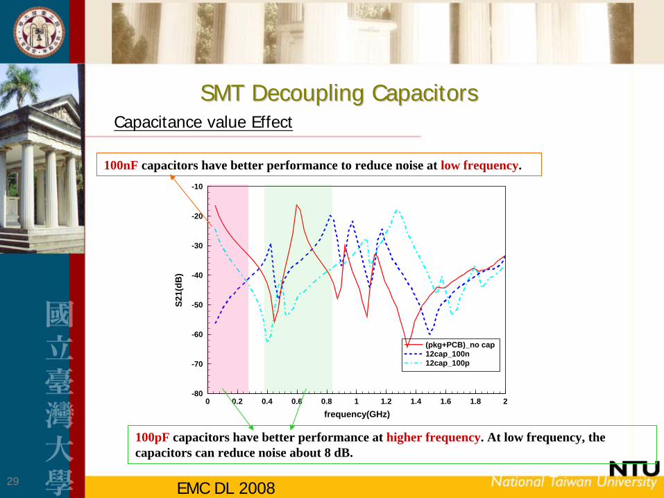
EMC DL 200829
0 0.2 0.4 0.6 0.8 1 1.2 1.4 1.6 1.8 2frequency(GHz)
-80
-70
-60
-50
-40
-30
-20
-10S2
1(dB
)
(pkg+PCB)_no cap12cap_100n12cap_100p
100nF capacitors have better performance to reduce noise at low frequency.
100pF capacitors have better performance at higher frequency. At low frequency, the capacitors can reduce noise about 8 dB.
SMT Decoupling CapacitorsSMT Decoupling CapacitorsCapacitance value Effect
EMC DL 200830
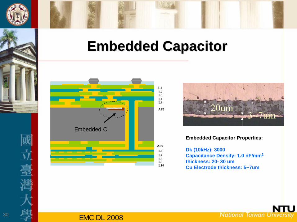
Embedded CapacitorEmbedded Capacitor
L1L2L3L4
AP5
L5
L6L7L8L9L10
AP6
Embedded CEmbedded Capacitor Properties:
Dk (10kHz): 3000Capacitance Density: 1.0 nF/mm2
thickness: 20- 30 umCu Electrode thickness: 5~7um
20um3~7um

EMC DL 200831 2008/8/1631
Caps locationCaps location
11
223344
77 88

EMC DL 20083232
Impedance measurement Impedance measurement
Cap (nF) ESL (pH) SRF (MHz)
Cap4 8.87 214 115.6
Good capacitor is seen below SRF.
SRF is in the several MHz range due to large ESL of the connecting vias.
The bandwidth could be enhanced by designing the capacitor closer to the surface of the package.

EMC DL 200833
GND plnae(2nd layer)
Vcc plane(3rd layer)
Substrate
Schematic diagram of the Isolated and BridgedPower Planes in Four Layers PCB Circuits
IC
Etched slit (Moat)
Bridged connection
X
Y
Z
Top layer (1'st layer)
Bottom layer (4th layer)
signal traces
Isolation by etched slot with bridgesIsolation by etched slot with bridges

EMC DL 200834
Isolation slots with bridgeIsolation slots with bridge
0 0.5 1 1.5 2 2.5 3Frequency(GHz)
-80
-70
-60
-50
-40
-30
-20
-10
0
|S12
| (dB
)
Dotted line: measurementSolid line: 3D-FDTDexcited location: port 2
reference board
0 0.5 1 1.5 2 2.5 3Frequency(GHz)
-80
-70
-60
-50
-40
-30
-20
-10
0
|S12
| (dB
)
moat-bridged board
33
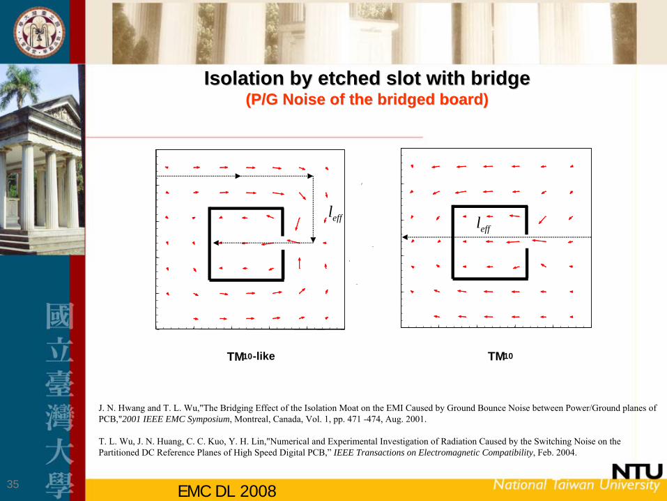
EMC DL 200835
effl
TM10
effl
TM10-like
Isolation by etched slot with bridgeIsolation by etched slot with bridge (P/G Noise of the bridged board)(P/G Noise of the bridged board)
J. N. Hwang and T. L. Wu,"The Bridging Effect of the Isolation Moat on the EMI Caused by Ground Bounce Noise between Power/Ground planes of PCB,"2001 IEEE EMC Symposium, Montreal, Canada, Vol. 1, pp. 471 -474, Aug. 2001.
T. L. Wu, J. N. Huang, C. C. Kuo, Y. H. Lin,"Numerical and Experimental Investigation of Radiation Caused by the Switching Noise on the Partitioned DC Reference Planes of High Speed Digital PCB,”
IEEE Transactions on Electromagnetic Compatibility, Feb. 2004.
36
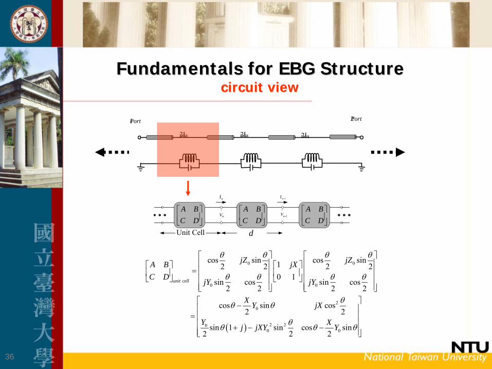
Fundamentals for EBG StructureFundamentals for EBG Structure circuit viewcircuit view
DGS2L DGS2L DGS2L
1Port 2Port
A BC D⎡ ⎤⎢ ⎥⎣ ⎦
A BC D⎡ ⎤⎢ ⎥⎣ ⎦
A BC D⎡ ⎤⎢ ⎥⎣ ⎦
Unit Cell d
nV+
−
1nV+
−
+
nI 1nI +
( )
0 0
0 0
20
2 200 0
cos sin cos sin12 2 2 20 1sin cos sin cos
2 2 2 2
cos sin cos2 2
sin 1 sin cos sin2 2 2
unit cell
jZ jZA B jXC D jY jY
X Y jX
Y Xj jXY Y
θ θ θ θ
θ θ θ θ
θθ θ
θθ θ θ
⎡ ⎤ ⎡ ⎤⎢ ⎥ ⎢ ⎥⎡ ⎤ ⎡ ⎤
= ⎢ ⎥ ⎢ ⎥⎢ ⎥ ⎢ ⎥⎣ ⎦ ⎣ ⎦⎢ ⎥ ⎢ ⎥
⎢ ⎥ ⎢ ⎥⎣ ⎦ ⎣ ⎦⎡ ⎤−⎢ ⎥
= ⎢ ⎥⎢ ⎥+ − −⎢ ⎥⎣ ⎦

37
Fundamentals for EBG StructureFundamentals for EBG Structure circuit viewcircuit view
0 0,α β π= ≠• Case 1 : (Pass Band)
0cos cos sin2Xd Zβ θ θ= −
0cos sin 12X Zθ θ− ≤
• Case 2 : (Stop Band)
0 =0,α β π≠
0cosh cos sin 12Xd Zα θ θ= − ≥
0 2 4 6 80
1
2
3
4
5
0
2
βd(r
ad)
αd(
Np)
Frequency(GHz)

38
Fundamentals for EBG/PBG StructureFundamentals for EBG/PBG Structure wave viewwave view
1D
2D3D

39 39
Fundamentals for EBG/PBG StructureFundamentals for EBG/PBG Structure wave viewwave view
1D example (no DK contrast)

40 40
Photonic Bandgap
Photonic Bandgap
Fundamentals for EBG/PBG StructureFundamentals for EBG/PBG Structure wave viewwave view
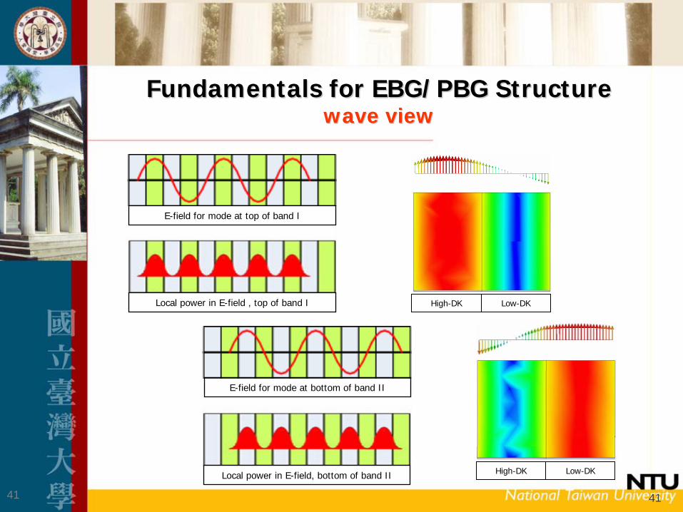
41 41
E-field for mode at top of band I
Local power in E-field , top of band I
E-field for mode at bottom of band II
Local power in E-field, bottom of band II
High-DK Low-DK
High-DK Low-DK
Fundamentals for EBG/PBG StructureFundamentals for EBG/PBG Structure wave viewwave view
42
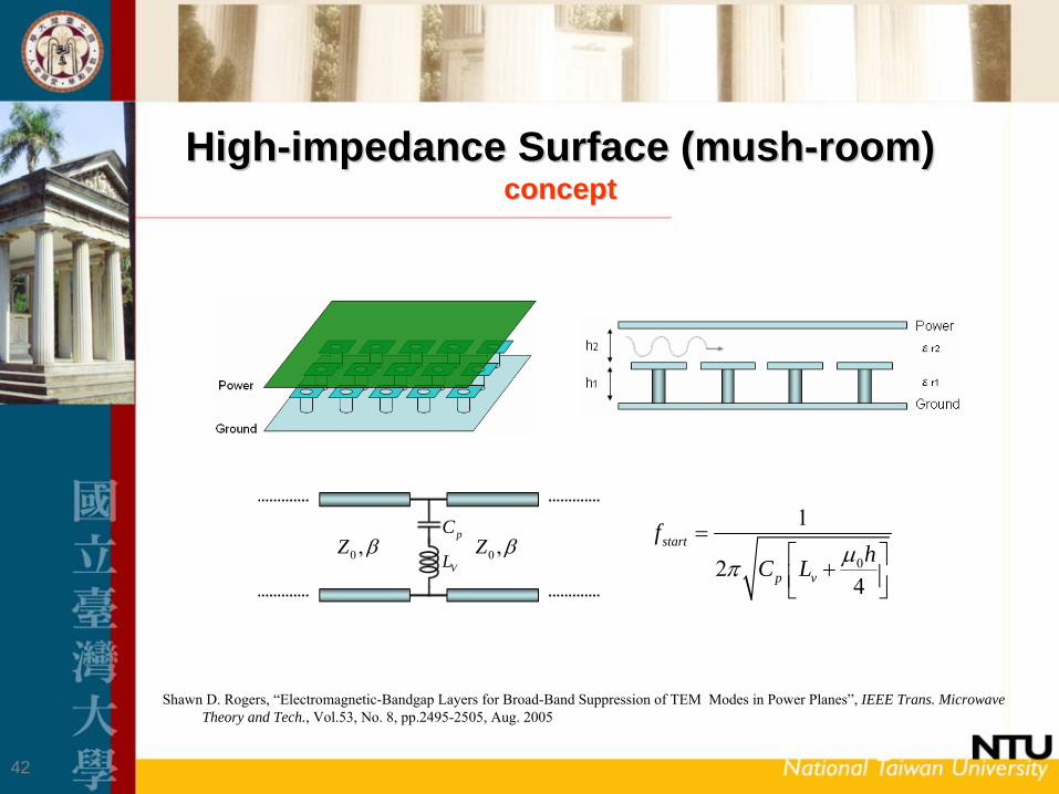
HighHigh--impedance Surface (mushimpedance Surface (mush--room)room) conceptconcept
0 ,Z β 0 ,Z βVL
pC
0
1
24
start
p v
fhC L μπ
=⎡ ⎤+⎢ ⎥⎣ ⎦
Shawn D. Rogers, “Electromagnetic-Bandgap Layers for Broad-Band Suppression of TEM Modes in Power Planes”, IEEE Trans. Microwave Theory and Tech., Vol.53, No. 8, pp.2495-2505, Aug. 2005

43
HighHigh--impedance Surface (mushimpedance Surface (mush--room)room) bandwidth enhancementbandwidth enhancement
Cascaded HIS: to improve the bandwidth
Shahrooz Shahparnia
and Omar M. Ramahi, “Electromagnetic Interference (EMI) Reduction From Printed Circuit Boards (PCB) Using Electromagnetic Bandgap Structures”, IEEE Trans. Electromagntic Compatibility, Vol.46, No.4, Nov. 2004.

44
HighHigh--impedance Surface (mushimpedance Surface (mush--room)room) bandwidth enhancementbandwidth enhancement
(d) Spiral HIS
(c) Double-Stacked HIS
Jongbae Park, Albert Chee W. Lu, Kai M. Chua, Lai L. Wai, Junho Lee, and Joungho Kim, “Double-Stacked EBG Structure for Wideband Suppression of Simultaneous Switching Noise in LTCC-Based SiP Applications”, IEEE Microwave and Wireless Components Letters, vol. 15, No.8, pp. 505-507, Aug. 2005. Chien-Lin Wang, Guang-Hwa Shiue, and Ruey-Beei Wu, “EBG-Enhanced Split Power Planes for Wideband Noise Suppression”, Proc. IEEE 14th Topical Meeting Elect. Performance Electron. Package., 2005, pp.61-64.
EMC DL 200845
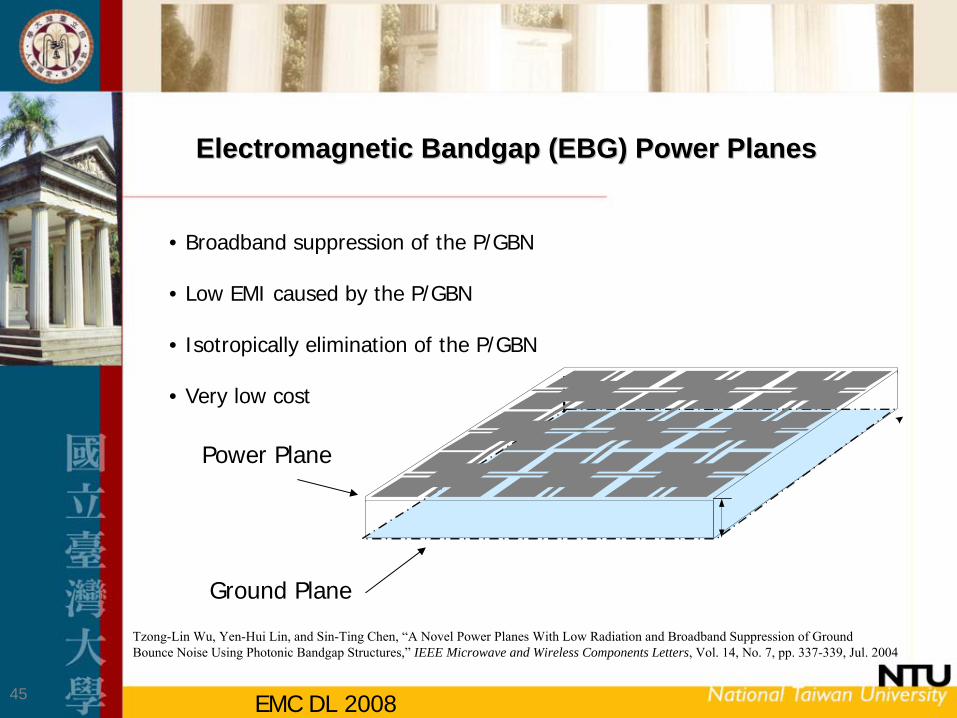
Electromagnetic Bandgap (EBG) Power PlanesElectromagnetic Bandgap (EBG) Power Planes
• Broadband suppression of the P/GBN
• Low EMI caused by the P/GBN
• Isotropically elimination of the P/GBN
• Very low cost
Ground Plane
Power Plane
Tzong-Lin Wu, Yen-Hui Lin, and Sin-Ting Chen, “A Novel Power Planes With Low Radiation and Broadband Suppression of Ground Bounce Noise Using Photonic Bandgap Structures,”
IEEE Microwave and Wireless Components Letters, Vol. 14, No. 7, pp. 337-339, Jul. 2004
EMC DL 200846
bLpC
gC
bC2 1ni − 2ni 2 1ni + 2 2ni +
2 2
2 2
n
nQ −
−
2 1
2 1
n
nQ −
−
2
2
n
nQ 2 1
2 1
n
nQ +
+
2 2
2 2
n
nQ +
+
gC gCpL
pC pCbCbC
bLbL
2 2ni −
pL pL pL
2 3
2 3
n
nQ +
+
2 3ni +
4.3rε =w
2pl
d
1p
1D1D--equivalent circuit modelequivalent circuit model
40

EMC DL 200847
90mm
90mm
Power plane
GND plane
h = 0.4mmx
y
z
(0,0)
0 1 2 3 4 5 6Frequency(GHz)
-110
-90
-70
-50
-30
-10
|S21
| (dB
)
Solid line: 2D-FDTDDotted line: measurement
Reference board
9-cell LPC-EBG boardexcited location: (45mm, 45mm)
received location: (15mm, 75mm)
P/GBN suppressionP/GBN suppression—— Frequency domainFrequency domain
44

EMC DL 200848
0 5 10 15 20 25 30Time(ns)
-0.4
-0.3
-0.2
-0.1
0
0.1
0.2
0.3
0.4
0.5
Volta
ge(m
V)
Reference board9-cell LPC-EBG board
excited source: 20mV Gaussian pulse
excited location: (45mm, 45mm)
received location: (15mm, 75mm)
90mm
90mm
Power plane
GND plane
h = 0.4mmx
y
z
(0,0)
P/GBN suppressionP/GBN suppression—— Time domain (3DTime domain (3D--FDTD)FDTD)
There is over 35% of the GBN suppression rate by LPC-EBG power plane design.
46
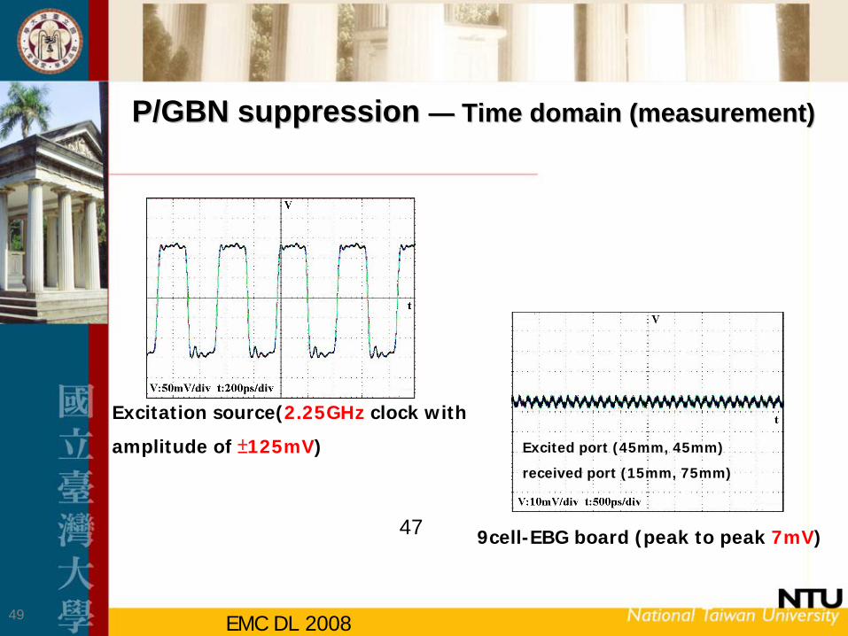
EMC DL 200849
Excitation source(2.25GHz clock with
amplitude of ±125mV)
P/GBN suppression P/GBN suppression —— Time domain (measurement)Time domain (measurement)
9cell-EBG board (peak to peak 7mV)
Excited port (45mm, 45mm)
received port (15mm, 75mm)
47
EMC DL 200850
0 0.5 1 1.5 2 2.5 3 3.5 4Frequency(GHz)
0
10
20
30
40
50
60
70
E_m
ax(d
BuV
/m)
EMI at 3mSolid line: 3D-FDTDDotted line: measurement
Reference board
9-cell LPC-EBG board
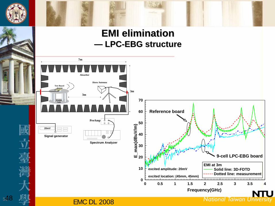
excited amplitude: 20mV
excited location: (45mm, 45mm)
PreAmp
Horn Antenna
Absorber
20mV
Spectrum Analyzer
Signal generator
3m
7m
Test Board
3m
Wooden Table
EMI eliminationEMI elimination —— LPCLPC--EBG structureEBG structure
48

EMC DL 200851
Port1
30mm
20mm
10mm
0.4mm
0.4mm
0.4mm
4.3rε =
(45mm, 49mm)
Port2
w=0.75mmPort1
30mm
20mm
10mm
0.4mm
0.4mm
0.4mm
4.3rε =
w=0.5mm
(45mm, 49mm)
Port2Port4
Port3
s=0.25mm
MEO=363mV MEW=370ps MEO=471mV MEW=389ps
Reference board (with solid power/ground planes)
MEO=440mV MEW=388ps
Impact on SI Impact on SI —— Traces referring to EBG planesTraces referring to EBG planes
49
Tzong-Lin Wu, Yen-Hui Lin, Ting-Kuang Wang, Chien-Chung Wang, and Sin-Ting Chen, “Electromagnetic Bandgap Power/Ground Planes for Wideband Suppression of Ground Bounce Noise and Radiated Emission in High-speed Circuits,”
IEEE Transactions on Microwave Theory and Techniques, vol. 53, No. 9, pp. 2935 -
2942, Sept. 2005
EMC DL 200852
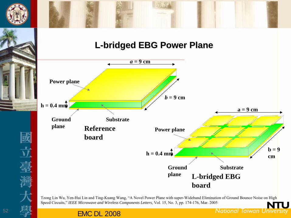
LL--bridged EBG Power Planebridged EBG Power Plane
L-bridged EBG board
Power plane
h = 0.4 mm
Ground plane
Substrate
b = 9 cm
a = 9 cm
Reference board
Power plane
Ground plane
Substrate
h = 0.4 mm
a = 9 cm
b = 9 cm
Tzong Lin Wu, Yen-Hui Lin and Ting-Kuang Wang, “A Novel Power Plane with super-Wideband Elimination of Ground Bounce Noise on High Speed Circuits,”
IEEE Microwave and Wireless Components Letters, Vol. 15, No. 3, pp. 174-176, Mar. 2005
EMC DL 200853
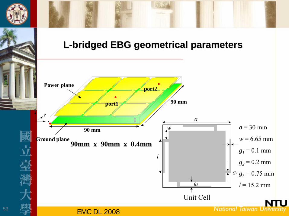
LL--bridged EBG geometrical parametersbridged EBG geometrical parameters
Power plane
Ground plane90mm x 90mm x 0.4mm
port1
port2
90 mm
90 mm
Unit Cell
g3
w
l
a
g2
a = 30 mm
w = 6.65 mm
g1 = 0.1 mm
g2 = 0.2 mm
g3 = 0.75 mm
l = 15.2 mm

EMC DL 200854
Wideband suppressionWideband suppression
0 1 2 3 4 5 6Frequency(GHz)
-100
-80
-60
-40
-20
0S 2
1(dB
)
FDTDFEMMeasurement
reference
L-bridged

EMC DL 200855
EMI performanceEMI performance
0.05 0.55 1.05 1.55 2.05 2.55Frequency (GHz)
5
10
15
20
25
30
35
40
45
50
Ez a
t 3m
(dB
uv/m
)
MeasurementreferenceL-bridged
EMC DL 200856
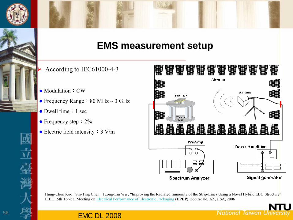
EMS measurement setupEMS measurement setup
According to IEC61000-4-3
Modulation:CW
Frequency Range:80 MHz ~ 3 GHz
Dwell time:1 sec
Frequency step:2%
Electric field intensity:3 V/m
Hung-Chun Kuo
Sin-Ting Chen
Tzong-Lin Wu
, “Improving the Radiated Immunity of the Strip-Lines Using a Novel Hybrid EBG Structure“, IEEE 15th Topical Meeting on Electrical Performance of Electronic Packaging
(EPEP), Scottsdale, AZ, USA, 2006
EMC DL 200857
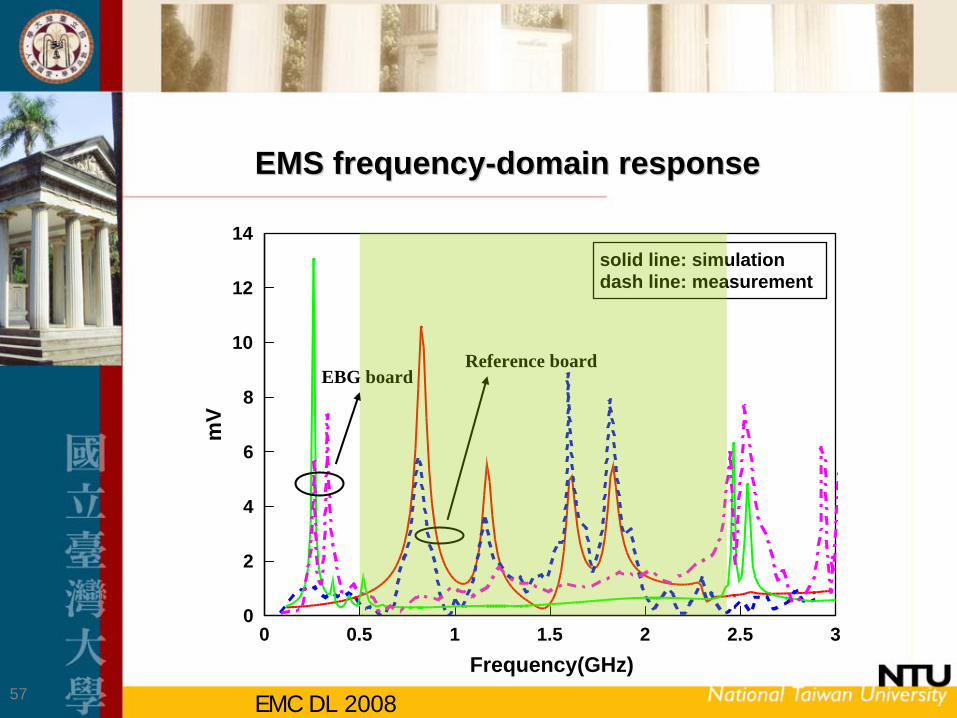
EMS frequencyEMS frequency--domain responsedomain response
0 0.5 1 1.5 2 2.5 3Frequency(GHz)
0
2
4
6
8
10
12
14m
V
solid line: simulationdash line: measurement
Reference boardEBG board
EMC DL 200858
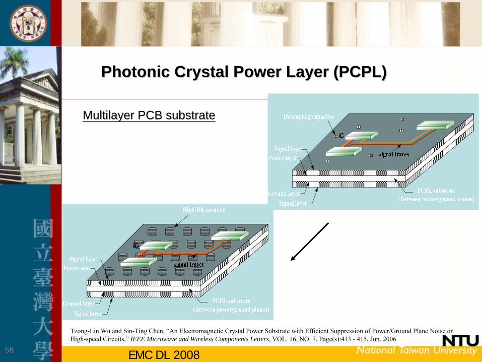
Photonic Crystal Power Layer (PCPL)Photonic Crystal Power Layer (PCPL)
Multilayer PCB substrateMultilayer PCB substrate
Tzong-Lin Wu and Sin-Ting Chen, “An Electromagnetic Crystal Power Substrate with Efficient Suppression of Power/Ground Plane Noise on High-speed Circuits,”
IEEE Microwave and Wireless Components Letters, VOL. 16, NO. 7, Page(s):413 -
415, Jun. 2006
EMC DL 200859
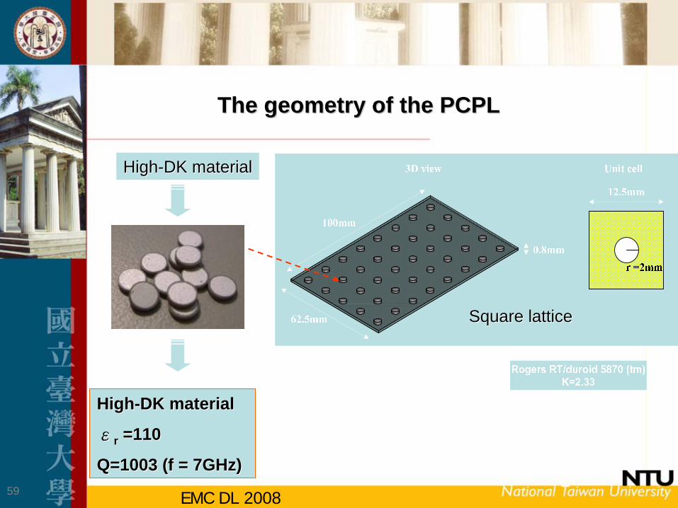
Square latticeSquare lattice
The geometry of the PCPLThe geometry of the PCPL
HighHigh--DK materialDK material
HighHigh--DK material DK material
εεrr =110=110
Q=1003 (f = 7GHz)Q=1003 (f = 7GHz)
EMC DL 200860
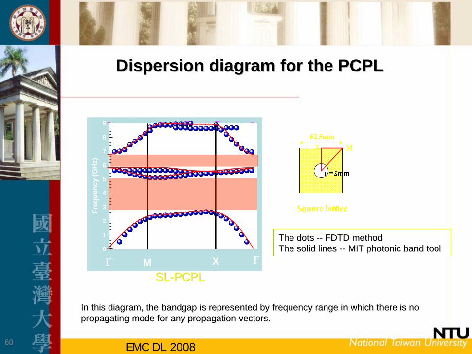
Dispersion diagram for the PCPLDispersion diagram for the PCPL
In this diagram, the In this diagram, the bandgapbandgap is represented by frequency range in which there is no is represented by frequency range in which there is no propagating mode for any propagation vectors.propagating mode for any propagation vectors.
The dots The dots ---- FDTD methodFDTD methodThe solid lines The solid lines ---- MIT photonic band tool MIT photonic band tool 0
1
2
3
4
5
6
7
8
9
Freq
uenc
y (G
Hz)
Γ ΓM XSLSL--PCPLPCPL
EMC DL 200861
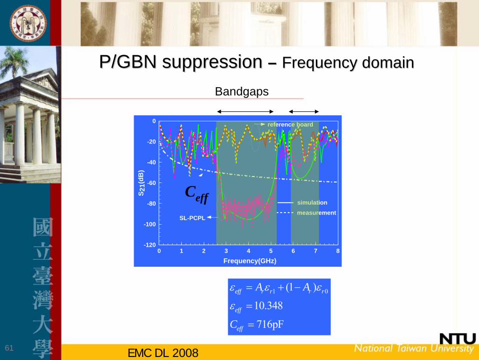
0 1 2 3 4 5 6 7 8Frequency(GHz)
-120
-100
-80
-60
-40
-20
0
S 21(
dB)
simulationmeasurement
reference board
SL-PCPL
Ceff
P/GBN suppressionP/GBN suppression –– Frequency domainFrequency domain
1 0(1 )
10.348
716pF
eff r r r r
eff
eff
A A
C
ε ε ε
ε
= + −
=
=
Bandgaps

EMC DL 200862
0 0.2 0.4 0.6 0.8 1Time (ns)
-200
-150
-100
-50
0
50
100
150
200
mv
0 0.2 0.4 0.6 0.8 1Time (ns)
-200
-150
-100
-50
0
50
100
150
200
mv
Reference boardSL-PCPL
The waveform of the excitation sourceThe waveform of the excitation source10Gbps and amplitude10Gbps and amplitude ±±125 125 mVmV
Square latticeSquare lattice
171.2 mV
16.1 mV
SSN can be reduced about 91%
P/GBN suppressionP/GBN suppression –– Time domainTime domain
EMC DL 200863
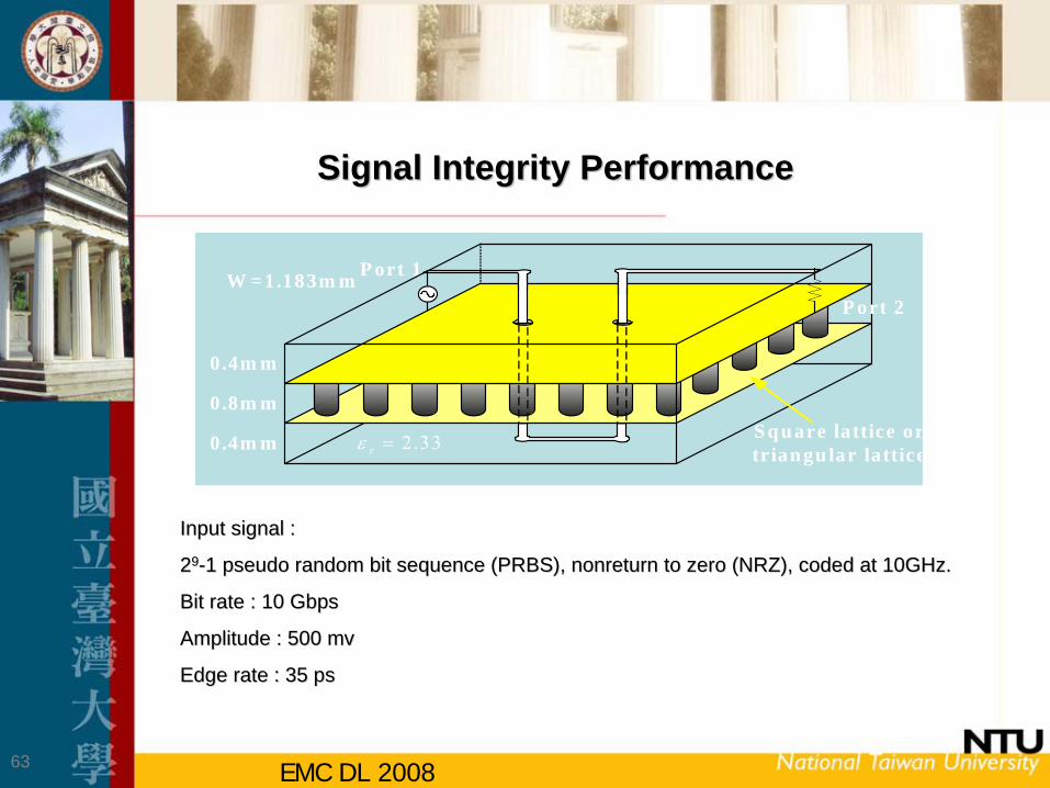
Signal Integrity PerformanceSignal Integrity Performance
2.33rε =
0.4m m
0.8m m
0.4m m
P ort 1W = 1.183m mP ort 2
S q u are lattice ortrian gu lar lattice
Input signal : Input signal :
2299--1 pseudo random bit sequence (PRBS), 1 pseudo random bit sequence (PRBS), nonreturnnonreturn to zero (NRZ), coded at 10GHz. to zero (NRZ), coded at 10GHz.
Bit rate : 10 Bit rate : 10 GbpsGbps
Amplitude : 500 Amplitude : 500 mvmv
Edge rate : 35 Edge rate : 35 psps
EMC DL 200864
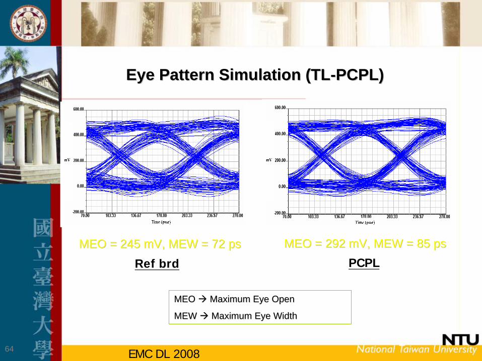
Eye Pattern Simulation (TLEye Pattern Simulation (TL--PCPL)PCPL)
MEO = 292 mV, MEW = 85 MEO = 292 mV, MEW = 85 pspsMEO = 245 mV, MEW = 72 MEO = 245 mV, MEW = 72 psps
MEO MEO Maximum Eye OpenMaximum Eye Open
MEW MEW Maximum Eye WidthMaximum Eye Width
PCPLRef brd
EMC DL 200865
1 2 3 4 5 6 7 8Frequency (GHz)
40
50
60
70
80
90
100
110
EMI (
dBuv
/m)
reference board
SL-PCPL
measurementsimulation
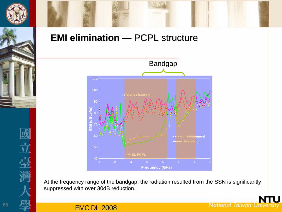
EMI eliminationEMI elimination —— PCPL structurePCPL structure
At the frequency range of the At the frequency range of the bandgapbandgap, the radiation resulted from the SSN is significantly , the radiation resulted from the SSN is significantly suppressed with over 30dB reduction.suppressed with over 30dB reduction.
Bandgap
EMC DL 200866
0 0.05 0.1 0.15 0.2 0.25 0.3 0.35 0.4 0.45r/a
0.05
0.1
0.15
0.2
0.25
0.3
0.35
0.4
Freq
uenc
y (£
sa/2
£kC
)
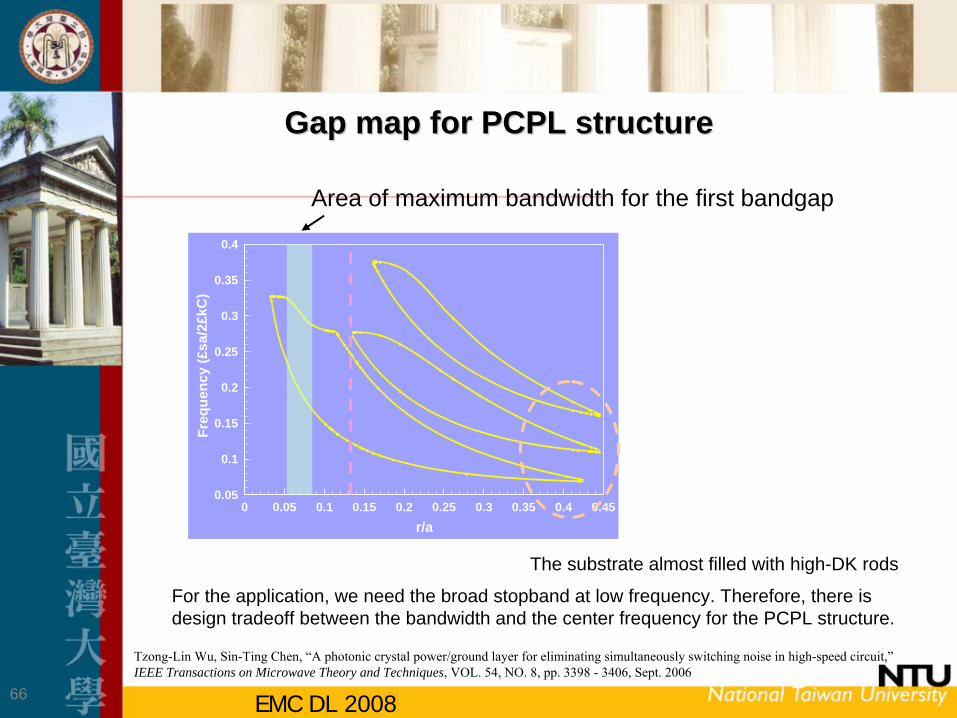
Gap map for PCPL structureGap map for PCPL structure
Area of maximum bandwidth for the first bandgap
The substrate almost filled with high-DK rods
For the application, we need the broad stopband at low frequency. Therefore, there is design tradeoff between the bandwidth and the center frequency for the PCPL structure.
Tzong-Lin Wu, Sin-Ting Chen, “A photonic crystal power/ground layer for eliminating simultaneously switching noise in high-speed circuit,”IEEE Transactions on Microwave Theory and Techniques, VOL. 54, NO. 8, pp. 3398 -
3406, Sept. 2006
EMC DL 200867
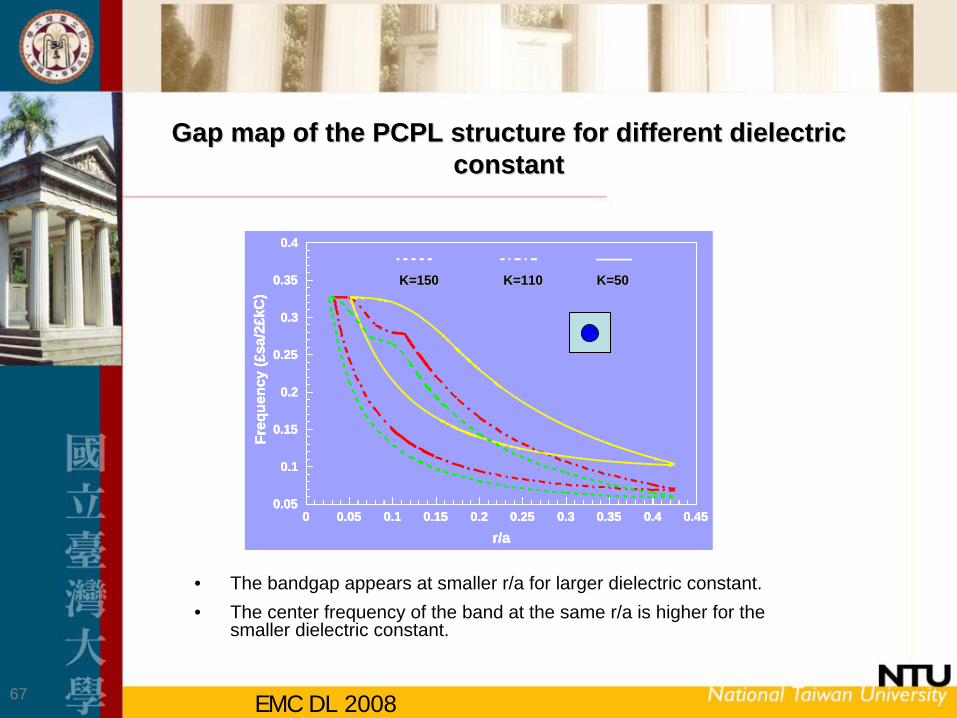
Gap map of the PCPL structure for different dielectric Gap map of the PCPL structure for different dielectric constantconstant
• The bandgap appears at smaller r/a for larger dielectric constant.• The center frequency of the band at the same r/a is higher for the
smaller dielectric constant.
0 0.05 0.1 0.15 0.2 0.25 0.3 0.35 0.4 0.45r/a
0.05
0.1
0.15
0.2
0.25
0.3
0.35
0.4Fr
eque
ncy
(£sa
/2£k
C)
K=150K=150 K=110K=110 K=50K=50
0 0.05 0.1 0.15 0.2 0.25 0.3 0.35 0.4 0.45r/a
0.05
0.1
0.15
0.2
0.25
0.3
0.35
0.4Fr
eque
ncy
(£sa
/2£k
C)
0 0.05 0.1 0.15 0.2 0.25 0.3 0.35 0.4 0.45r/a
0.05
0.1
0.15
0.2
0.25
0.3
0.35
0.4Fr
eque
ncy
(£sa
/2£k
C)
EMC DL 200868
ConclusionConclusion
• P/GBN is one of the key issues for designing high-speed digital circuit with good signal integrity (SI) and EMC performance.
• Several approaches to eliminate the P/GBN on the power delivery systems are investigated by both numerical simulations and experimental measurement.


