
University of Central Florida University of Central Florida
STARS STARS
Electronic Theses and Dissertations, 2004-2019
2005
Preparation And Characterization Of Cigss Solar Cells And Pv Preparation And Characterization Of Cigss Solar Cells And Pv
Module Data Analysis Module Data Analysis
Jyoti Shirolikar University of Central Florida
Part of the Electrical and Electronics Commons
Find similar works at: https://stars.library.ucf.edu/etd
University of Central Florida Libraries http://library.ucf.edu
This Masters Thesis (Open Access) is brought to you for free and open access by STARS. It has been accepted for
inclusion in Electronic Theses and Dissertations, 2004-2019 by an authorized administrator of STARS. For more
information, please contact [email protected].
STARS Citation STARS Citation Shirolikar, Jyoti, "Preparation And Characterization Of Cigss Solar Cells And Pv Module Data Analysis" (2005). Electronic Theses and Dissertations, 2004-2019. 619. https://stars.library.ucf.edu/etd/619

PREPARATION AND CHARACTERIZATION OF CIGSS SOLAR CELLS AND PV MODULE DATA ANALYSIS
by
JYOTI SHIROLIKAR B.E. (Electronics and Telecommunication), University of Pune, 2001
A thesis submitted in partial fulfillment of the requirements for the degree of Master of Science
in the Department of Electrical Engineering in the College of Engineering and Computer Science
at the University of Central Florida Orlando, Florida
Fall Term 2005

© 2004 Jyoti Shirolikar
ii
ABSTRACT
In this thesis, multiple activities have been carried out in order to improve the
process of CIGSS solar cell fabrication on a 4” x 4” substrate. The process of CIGSS
solar cell fabrication at FSEC’s PV Materials Lab involves a series of steps that were all
carried out manually in the past. A LABVIEW program has been written to carry out
automated sputter deposition of Mo back contact, CuGa, In metallic precursors on a soda
lime glass substrate using a stepper motor control for better uniformity. Further,
selenization/ sulfurization of these precursors was carried out using rapid thermal
processing (RTP). CIGS films were sulfurized using chemical bath deposition (CBD).
ZnO:Al was deposited on the CIGSS films using RF sputtering. A separate LABVIEW
program was written to automate the process of ZnO:Al deposition. Ni/Al contact
fingers were deposited on the ZnO:Al layer using the e-beam evaporation technique.
Further, in order to test these solar cells in-house, a simple current-voltage (IV)
tracer was fabricated using LABVIEW. A quantum efficiency (QE) measurement setup
was built with guidance from the National Renewable Energy Laboratory (NREL).
Lastly, analysis of data from photovoltaic (PV) modules installed on the FSEC
test site has been carried out using a LABVIEW program in order to find out their rate of
degradation as time progresses. A ‘C’ program has also been written as an aid for
keeping a daily log of errors in data and for troubleshooting of the same.
iii

.
To my parents and grandparents,
For the values they instilled in me.
iv

ACKNOWLEDGMENTS
I would like to express my deepest gratitude to my thesis advisor Dr. Neelkanth
G. Dhere for making it possible for me to pursue graduate studies at the prestigious
University of Central Florida (UCF) and for giving me the opportunity to independently
complete a variety of tasks at the Florida Solar Energy Center (FSEC). I am indebted to
him for his guidance and motivation. I would like to thank my academic advisor Dr.
Kalpathy Sundaram and Dr. Issa Batarseh at the Department of Electrical Engineering for
serving on my final examination committee and for their invaluable suggestions. I would
like to thank Keith Emery and Clay De Hart at the National Renewable Energy
Laboratory (NREL) for their assistance in setting up the equipment for quantum
efficiency (QE) measurement and current-voltage (IV) testing of solar cells.
My colleagues at FSEC have always been a great help and source of inspiration to
me. Special thanks to Mr. Ankur Kadam, Mr. Anant Jahagirdar, Mr. Vinay Hadagali,
Mr. Sachin Kulkarni, Mr. Upendra Avachat, , Mr. Shirish Pethe, Mr. Parag Vasekar and
others at FSEC. Mr. Matthew Nugent and Mr. Robert Hodge came up with wonderful
ideas and ways to implement them when we were building the QE setup and deposition
mechanism and the rapid thermal processing setup respectively.
Words are not enough to express my gratitude towards my parents and
grandparents who have always been supportive of my aspirations.
v

TABLE OF CONTENTS
LIST OF FIGURES ........................................................................................................... ix
LIST OF TABLES............................................................................................................ xii
LIST OF ACRONYMS/ABBREVIATIONS.................................................................. xiii
CHAPTER ONE: INTRODUCTION................................................................................. 1
Solar energy and photovoltaics........................................................................................1
Photovoltaics- Theory of operation .................................................................................2
Energy band diagram .......................................................................................................4
Current-voltage (I-V) characteristics of a solar cell ........................................................8
Types of thin-film solar cells .........................................................................................12
CHAPTER TWO: LITERATURE REVIEW................................................................... 14
Thin-film solar cells.......................................................................................................14
The CIGS absorber layer ...............................................................................................14
Rapid Thermal Processing of CIGSS solar cells ...........................................................17
CHAPTER THREE: SOFTWARE DEVELOPMENT FOR AUTOMATION ............... 19
Automation of deposition of Mo, CIG layers ................................................................19
Current-voltage (IV) measurement setup.......................................................................33
Description of the block diagram for IV.vi....................................................................37
Regression analysis of PV module data.........................................................................44
C program for error checking of data ............................................................................47
vi

CHAPTER FOUR: CONSTRUCTION OF SETUPS – RTP and QE.............................. 49
Rapid Thermal Processing Unit .....................................................................................49
Quantum Efficiency measurement setup .......................................................................52
CHAPTER FIVE: EXPERIMENTAL TECHNIQUE...................................................... 57
Fabrication process for CIGSS solar cells .....................................................................57
Substrate preparation .....................................................................................................58
Deposition of CuGa and In layers..................................................................................58
Thermal evaporation of NaF and Se ..............................................................................59
Heat treatment of the precursor film..............................................................................62
Chemical bath deposition of CdS layer .........................................................................63
Deposition of transparent conducting ZnO/ZnO:Al window bilayer ............................65
Deposition of Ni/Al contact fingers...............................................................................65
Scribing and soldering of In ribbons..............................................................................66
CHAPTER SIX: RESULTS AND DISCUSSION ........................................................... 68
Rapid Thermal Processing .............................................................................................68
Experiment 1............................................................................................................. 68
Experiment 2............................................................................................................. 71
Experiment 3............................................................................................................. 75
Experiment 4............................................................................................................. 77
Experiment 5............................................................................................................. 80
Experiment 6............................................................................................................. 81
CHAPTER SEVEN: CONCLUSIONS ............................................................................ 85
vii

APPENDIX A: C SOURCE CODE FOR PROGRAM TO CHECK PV MODULE DATA
........................................................................................................................................... 87
APPENDIX B: PROCEDURE FOR CdS THIN FILM DEPOSITION ON CIGS FILMS
........................................................................................................................................... 94
APPENDIX C: LIST OF ELECTRONIC COMPONENTS FOR AUTOMATION OF
DEPOSITION MECHANISM ......................................................................................... 97
APPENDIX D: LIST OF ELECTRONIC COMPONENTS FOR CURRENT-VOLTAGE
MEASUREMENT SETUP............................................................................................... 99
APPENDIX E: TEMPERATURE PROFILES FOR RTP SETUP ................................ 101
LIST OF REFERENCES................................................................................................ 104
viii

LIST OF FIGURES
Figure 1: Basic features of photovoltaic energy conversion. The check valve prevents
backflow of excited electrons. .................................................................................... 2
Figure 2: Energy level band diagram of semiconductors ................................................... 5
Figure 3: Energy band structure of a p-n junction .............................................................. 6
Figure 4 : p-n junction under forward bias and reverse bias............................................... 7
Figure 5: Typical current-voltage characteristics of a solar cell......................................... 9
Figure 6: Equivalent circuit of a solar cell........................................................................ 10
Figure 7: 18.8% efficient CIGS/CdS/ZnO solar cell ........................................................ 15
Figure 8: Photograph of PC running LABVIEW deposition program ............................. 19
Figure 9: Block diagram for deposition systems for CIG, Mo and ZnO/ZnO:Al............. 20
Figure 10: Connection diagram for stepper motor drive, power supply and stepper motor
................................................................................................................................... 22
Figure 11: User interface for stepper motor test program................................................. 22
Figure 12: Block diagram for stepper motor vi ................................................................ 24
Figure 13: Generate Pulse Train vi (built-in LABVIEW vi) ............................................ 25
Figure 14: User interface for enhanced LABVIEW program for CIG, Mo deposition.... 26
Figure 15: Lighting of LEDs according to current pass using integer-binary conversion 27
Figure 16: Deposition mechanism for CuGa, In, Mo ....................................................... 28
Figure 17: User interface for ZnO, ZnO:Al deposition chamber...................................... 29
Figure 18: Block Diagram for I-V measurement Setup.................................................... 31
Figure 19: Circuit Diagram for PCB with BUF04............................................................ 32
ix

Figure 20: Snapshot of LABVIEW program for I-V measurement ................................. 33
Figure 21: I-V measurement setup.................................................................................... 34
Figure 22: Graphical User Interface for the I-V measurement program .......................... 35
Figure 23: Plotting I-V data .............................................................................................. 36
Figure 24: Retrieving dark and light I-V data................................................................... 37
Figure 25: IVchar.llb......................................................................................................... 38
Figure 26: Block diagram for IV.vi .................................................................................. 39
Figure 27: Block diagram of IVmeas.vi .......................................................................... 41
Figure 28: GPIB write....................................................................................................... 41
Figure 29: GPIB read ........................................................................................................ 42
Figure 30: Block diagram of IVgraph.vi........................................................................... 43
Figure 31: Graphical User Interface for Regression Analysis program ........................... 44
Figure 32: Block diagram for regression analysis LABVIEW program .......................... 46
Figure 33: Plot of PTC power versus month of the year. PTC values were calculated
using the regression analysis program. ..................................................................... 47
Figure 34: Execution of error-checking program for downloaded .DAT file................... 48
Figure 35: Schematic of RTP setup .................................................................................. 49
Figure 36: Electrical connections for infrared lamp array. ............................................... 50
Figure 37: AUTOCAD drawing for graphite tray ............................................................ 51
Figure 38: Rapid Thermal Processing setup ..................................................................... 51
Figure 39: Block diagram for Quantum Efficiency measurement setup .......................... 54
Figure 40: GUI of QE measurement vi............................................................................. 55
Figure 41: Plot of QE vs wavelength................................................................................ 55
x

Figure 42: Flowchart for Quantum Efficiency measurement LABVIEW program ......... 56
Figure 43: CIGSS solar cell fabrication process............................................................... 57
Figure 44: Principle of deposition by sputtering............................................................... 59
Figure 45: Thermal evaporation setup .............................................................................. 60
Figure 46: Before Se evaporation ..................................................................................... 61
Figure 47: After Se evaporation........................................................................................ 61
Figure 48: Chemical bath deposition of CdS layer........................................................... 64
Figure 49: Layer sequence of Cu(In, Ga)S2 thin-film solar cells...................................... 66
Figure 50: Solar cells after scribing and soldering indium ribbon................................... 67
Figure 51: EDS data for CIGS sample from Experiment 2 – run 2 (2D) ......................... 72
Figure 52: SEM photograph of CIGS sample from Experiment 2 – run 2 (2D) .............. 73
Figure 53: EDS data for CIGS sample of Experiment 2 – run 5 (2G).............................. 73
Figure 54: SEM photograph of CIGS thin film of Experiment 2-run 5 (2G) ................... 74
Figure 55: SEM photograph of unetched CIGS sample from Experiment 3.................... 75
Figure 56 :SEM photograph of etched CIGS sample from Experiment 3........................ 76
Figure 57: XEDS data for Experiment 4........................................................................... 79
Figure 58: SEM photograph for etched sample of Experiment 4 ..................................... 79
Figure 59: Photograph of CIGS film after thermal evaporation ....................................... 80
Figure 60: Temperature versus time graph for 100% power setting .............................. 102
Figure 61: Temperature versus time graph for 30% for 48 minutes, 40% for 3 minutes102
Figure 62: Temperature versus time graph for 35% power setting ................................ 103
xi

LIST OF TABLES
Table 1: Connections for CIG vacuum chamber (initial) ................................................. 21
Table 2: Connections for CIG and ZnO chamber (final).................................................. 23
Table 3: Deposition parameters for CuGa and In – Experiment 1 ................................... 68
Table 4: Evaporation parameters for Se and NaF – Experiment 1 ................................... 68
Table 5: Deposition parameters for CuGa and In – Experiment 2 ................................... 71
Table 6: Evaporation parameters for Se and NaF – Experiment 2 ................................... 71
Table 7: Deposition parameters for CuGa, In - Experiment 3.......................................... 75
Table 8: RTP temperature readings for Experiment 4 ...................................................... 77
Table 9: Deposition parameters for CuGa, In – Experiment 5 ......................................... 80
Table 10: Deposition parameters for Experiment 6.......................................................... 81
Table 11: RTP temperature readings for Experiment 6 .................................................... 82
xii

LIST OF ACRONYMS/ABBREVIATIONS
RTP Rapid Thermal Processing
QE Quantum efficiency
I-V Current-Voltage
PV Photovoltaic
CIGS copper indium-gallium diselenide
CIGSS copper indium-gallium selenide sulfide
DAQ data acquisition
TCO transparent conducting oxide
xiii

CHAPTER ONE: INTRODUCTION
Solar energy and photovoltaics
There is a widespread demand for new energy sources that are renewable,
environmentally acceptable and capable of direct conversion to electricity. Photovoltaic
energy conversion refers to the direct conversion of the energy in light into usable
electrical energy which may be employed immediately or stored [1]. The advantages of
a photovoltaic (solar) cell over conventional power systems are [2]:
1. Solar cells convert solar radiation directly into electricity using the photovoltaic
effect. There is no thermal process involved.
2. Solar cells are reliable, durable and generally maintenance free, hence suitable
even in isolated and remote areas.
3. Solar cells are quiet, benign, respond immediately to solar radiation and have an
expected lifetime of more than 20 years.
4. Solar cells can be located at the site of use and hence no distribution network is
required.
5. Solar cells are modular, thereby permitting scaling up of size as needed.
1

Photovoltaics- Theory of operation
Photovoltaic (PV) energy conversion can be represented by Figure 1 [1]. The
main ingredients of a PV energy conversion are: a light-induced transition from ground
state to excited state, a transport mechanism which conveys away the resulting excited
electrons and holes and a ‘check valve’ which prevents the backflow and recombination
of the photo-generated electrons and holes.
Check valve
Figure 1: Basic features of photovoltaic energy conversion. The check valve prevents
backflow of excited electrons.
h
h
To external application
Ground state
hν
e eExcited state
Electron transport
Hole transport
2

When one of the various man-made PV energy conversion systems represented by
Figure 1 is used to convert sunlight into electrical energy, it is termed as a solar cell.
PV cells employ semiconducting materials and are based on the formation of a
potential barrier, such as in a p-n junction. Semiconductors, like many other materials
can be in crystalline, polycrystalline or amorphous form. Crystalline and polycrystalline
materials possess a lattice structure. Amorphous materials lack long range order i.e.
there is no lattice. Polycrystalline materials are composed of many small single crystals
or crystallites.
To illustrate how a solar cell works, we consider a single crystal silicon (Si) cell.
Intrinsic Si contains impurity atoms with concentrations of <1018 m-3. The four valence
electrons are shared with adjacent Si atoms by covalent bonding. At absolute zero (0 K),
all four electrons are firmly bound and the Si crystal behaves like an insulator as no
electrons are free. However, if some energy is added to break the covalent bond, (Bond
energy = 1.1 eV for Si), the bond can be broken. When an electron breaks away from the
bond, a corresponding positive charge carrier (hole) is left behind. The flow of such
carriers through an external circuit constitutes an electric current. Si can also be doped
with a donor impurity e.g. phosphorus to obtain an n-type semiconductor in which the
majority carriers are electrons. A p-type semiconductor with holes as majority free
carriers is obtained by doping Si with an acceptor impurity e.g. boron.
If a p-type and n-type semiconductor is joined together, a p-n junction is formed
at the boundary because the electrons in the n-type region diffuse across the boundary
into the p-type region and recombine with holes there. Similarly, holes in the p-type
region diffuse across the boundary into the n-type region and recombine with electrons.
3

Hence, an electric field is established across the junction which opposes further diffusion
of free carriers. Light incident on the p-n junction generates mobile charge carriers. The
built-in electric field separates these charge carriers according to charge and sweeps them
out, setting up a current density J. Under short circuit conditions, this current density J
would have the value Jsc. Under open circuit conditions, the structure would have to bias
itself to an open circuit voltage Voc necessary to develop a current just able to counter the
light-caused current. J, Jsc and Voc are a result of the built-in electric field.
Energy band diagram
According to the Pauli exclusion principle, each allowed energy level can be
occupied at most by two electrons, each of opposite spin. This energy level is termed as
Fermi level FE . If the temperature increases, some of the electrons gain energy in excess
of the Fermi level and the electron distribution in the allowed levels can be described
using the Fermi-Dirac distribution function )(Ef :
⎟⎟⎟⎟⎟
⎠
⎞
⎜⎜⎜⎜⎜
⎝
⎛ −
+
=
kTEE
e
EfF)(
1
1)(
where E is the energy of an allowed state,
FE is the Fermi energy,
k is the Boltzmann constant,
T is the absolute temperature.
4

The Fermi energy level is the energy level at which the probability of a state
being filled by an electron is exactly one-half.
Ec (Conduction band) Ec
Electron energy
EF (Fermi level) ED
EF
EV (Valence band) EV (Valence band)
(a): Intrinsic semiconductor (b): Extrinsic n-type semiconductor
Ec
EF
EA
EV (c): Extrinsic p-type semiconductor
Figure 2: Energy level band diagram of semiconductors
In an intrinsic semiconductor, the Fermi level is exactly in the middle of the
energy gap. i.e. FE = 2
gE and there are equal number of electrons and holes. The
location of the Fermi level in an extrinsic material depends on the density of impurity
atoms per cubic centimeter present and the temperature.
5
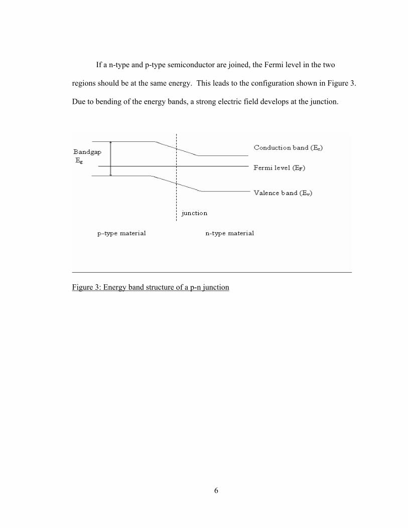
If a n-type and p-type semiconductor are joined, the Fermi level in the two
regions should be at the same energy. This leads to the configuration shown in Figure 3.
Due to bending of the energy bands, a strong electric field develops at the junction.
Figure 3: Energy band structure of a p-n junction
6

This electric field counterbalances the tendency for a large diffusion current from
the p-region to n-region. The p-n junction provides an inherent electric field to accelerate
electrons which could drift through the junction into the n-region.
Figure 4 shows the p-n junction under forward and reverse bias.
Figure 4 : p-n junction under forward bias and reverse bias
In the forward bias condition, holes from the p-region enter the n-region easily
and the internal energy barrier is reduced. Current flow rises sharply since many
electrons are available on the n-side and many holes are available on the p-side. In the
reverse bias condition, the inherent electric field becomes stronger, resulting in no flow
of current. A very small current flows through the p-n junction due to flow of electrons
from the p-region and holes from the n-region (minority carriers).
7

Current-voltage (I-V) characteristics of a solar cell
In the absence of light, the relation between the flow of junction current jI and
the externally applied voltage V in a p-n junction is given by:
)1(0 −= kTqV
j eII (1)
where q is the electronic charge, I0 is the reverse saturation current (dark current)
T is the temperature
The dark current is dominated by diffusion of minority carriers and is given as:
e
pe
h
nh
LnqD
LqDI p 00
0 += (2)
pn0, np0 are respectively the densities of holes on the n-side and electrons on the p-
side at thermal equilibrium
Lh, Le are the hole diffusion length on p-side and electron diffusion length on n-
side
Dh, De are the hole and electron diffusion constants respectively
D
in
A
ip
eh
ee
Nnp
Nnn
qkTD
qkTD
2
0
2
0 ,,, ==== µµ (3)
21
21
)(,)( hhheee DLDL ττ ==
τe and τh are the electron and hole lifetimes as minority carriers respectively.
When light is incident on the junction, electron-hole pairs are generated. The
electric current is now given by:
I = IL - Ij where IL is the light generated current (4)
8
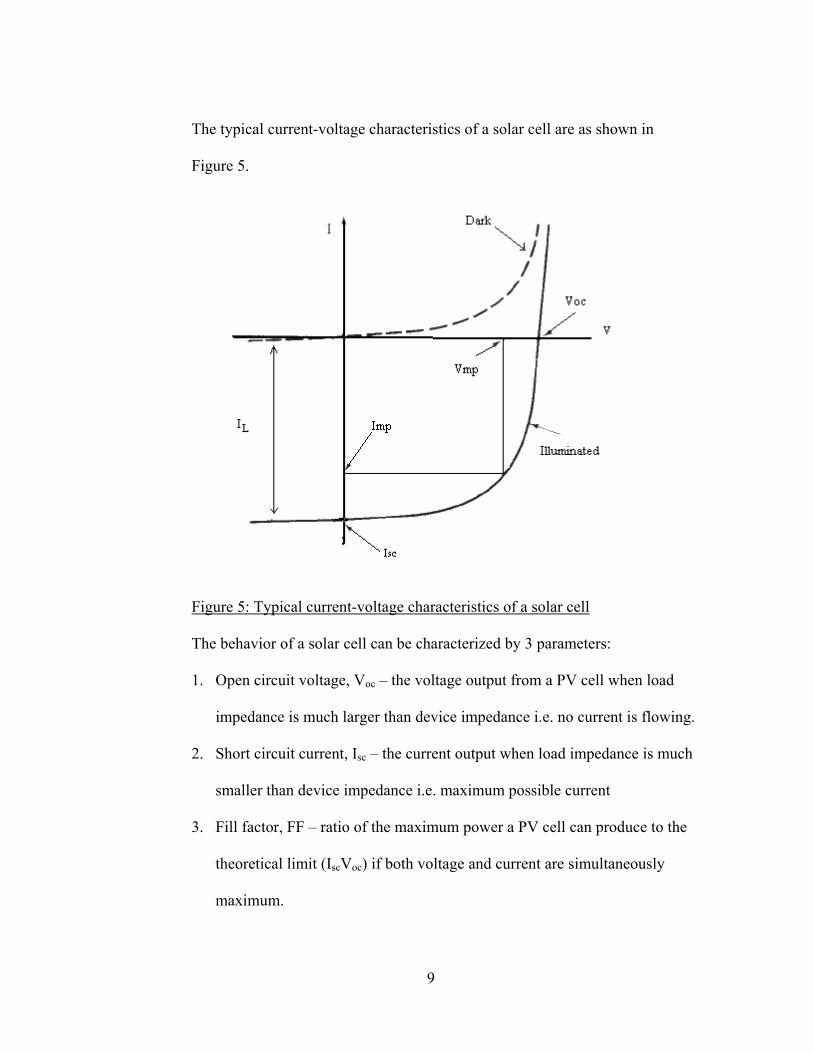
The typical current-voltage characteristics of a solar cell are as shown in
Figure 5.
Figure 5: Typical current-voltage characteristics of a solar cell
The behavior of a solar cell can be characterized by 3 parameters:
1. Open circuit voltage, Voc – the voltage output from a PV cell when load
impedance is much larger than device impedance i.e. no current is flowing.
2. Short circuit current, Isc – the current output when load impedance is much
smaller than device impedance i.e. maximum possible current
3. Fill factor, FF – ratio of the maximum power a PV cell can produce to the
theoretical limit (IscVoc) if both voltage and current are simultaneously
maximum.
9

whereocsc
m
VIVFF )I( m= (5)
The efficiency of the solar cell is given by in
m
PV )I( m×=η (6)
The equivalent circuit of a solar cell is shown in Figure 6. The current flow will
thus be:
)1(
)(
0 −−=
−
kT
IRsVq
eIII L (7)
The series resistance, Rs (series resistance) can be reduced to zero by proper
design of ohmic contact grid design and by making the diffusion region thin. As the
shunt resistance decreases, the fill factor and Voc decrease while Isc is not affected.
Rs
Rsh
Figure 6: Equivalent circuit of a solar cell
V oc of a p-n junction is related to the band gap Eg as:
)1ln(0+=
II
qkTV sc
oc (8)
I0 is a function of band gap Eg of the material and temperature T
With increase in Eg and decrease in T, I0 decreases and Voc increases.
Constant current generator
IL Ij
Diode junction
RL
10

Isc depends on the spectral response of the PV cells and the spectrum of light.
For maximum value of Voc, the diode saturation current should be as small as
possible. An estimation of the minimum value of saturation current, I0 in terms of band
gap is:
)(0
5105.1 kTEg
eI−
×= (9)
Thus, as the energy band gap decreases, the maximum value of Voc decreases
(opposite to Isc). There is an optimum band gap semiconductor for maximum efficiency.
At room temperature, the peak theoretical efficiency occurs for the band gap in the range
of 1.4 -1.6 eV. CdTe with the bandgap of 1.5 eV and GaAs with a bandgap of 1.4 eV are
near the optimum. Isc increases linearly with increase in light intensity while Voc
increases very rapidly and then becomes constant with increase in light intensity. At low
intensities, Rsh has a strong effect while at high intensities, Rs has a strong effect.
The solar spectrum radiation energy is dominant in the region of 2x10⁻⁷ – 4x10⁻⁶
m. A low band gap material absorbs a higher fraction of photons from the sunlight,
providing high Isc while a high band gap material will absorb a small fraction of photons
from sunlight but provide higher Voc.
11

Types of thin-film solar cells
Thin-film solar cells
polycrystalline epitaxial amorphous
Eg. CIGS, CdTe Eg. a-Si:H Eg. III-V
In case of crystalline Si (indirect band semiconductor), the cell thickness
necessary to absorb incident light is very large (100-200 µm) while in case of thin-film
solar cells (direct band semiconductor), a thickness of only 1-2 µm is required.
Commonly used materials for thin-film solar cells are II-VI or I-III-VI
compounds because of the following advantages [3]:
1. direct band gap, high optical absorption coefficient
2. moderate surface recombination velocities
3. ease of growth as thin films at low substrate temperatures
In case of solar cells based on CIGS (copper indium-gallium diselenide) or CdTe,
the front part of the junction is formed by a wide bandgap material (CdS window) which
transmits most of the incident light to the low bandgap absorber layer CuIn1-xGaxSe2 or
CdTe) where virtually all electron-hole pairs are produced and most of the power is
generated. The top contact is formed by a transparent conducting oxide (TCO) layer.
Techniques used for development of thin films are based on the principle that
vapor atoms impinging on a substrate lose their kinetic energy and are absorbed on the
12

surface. Thin films consist of a large number of grains of sizes ranging from 0.1-100 µm.
Grain boundaries give rise to recombination of minority carriers and thus degrade device
performance. They provide an easy diffusion path for mobile ions and atoms. This can
deteriorate device performance due to interdiffusion of certain atomic species or by
diffusion of a particular element from one surface to the other, causing shorting paths.
Thus it is desirable to neutralize the electrical activity of grain boundaries [4].
13

CHAPTER TWO: LITERATURE REVIEW
Thin-film solar cells
Large-scale application of PV systems has been impeded due to the high cost of
solar cell modules. Thin-film solar cells can be fabricated with low material use, few
processing steps, simple technology and have the potential to reduce the cost of solar
power from $7/Wp to $1.5/Wp. Thin-film technologies based on alloys of amorphous
Si(a-Si:H), cadmium telluride (CdTe), and ternary and multinary CIS are leading
contenders for large scale production, current production capacity being 35MW/y for a-
Si:H, more than 1 MW/y for CdTe and 100 kW/y for CIGS. The highest efficiency solar
cells have been made with III-V materials and their alloys [5].
The CIGS absorber layer
The 18.8% efficiency CIGS solar cell has the structure shown in Figure 7. CIGS
belongs to a class of diamond-like compounds and its structure is analogous to traditional
semiconductors. It has a bandgap of 1.04 eV. Development of chalcopyrite based solar
cells started in the early 1970s when Wagner et al realized a 12% efficient solar cell
based on a CuInSe2 single crystal [6]. Kazmerski et al [7] were able to demonstrate the
first thin-film solar cell by evaporation of CuInSe2 as a compound. CuInSe2 and its
alloys CuIn1-xGaxSe2-ySy provide the absorber material for the most efficient thin-film
14

solar cells. Doping of CuInSe2 is controlled by intrinsic defects. Samples with p-type
conductivity are grown if the material is Cu-poor and annealed under high Se vapor
pressure. Cu-rich material with Se deficiency tends to be n-type. Thus Se vacancy is
considered to be the dominant donor in n-type material. Cu vacancy is the dominant
acceptor in Cu-poor p-type material. The Cu content of device quality CuInSe2 absorbers
varies between 22 and 24% at. Cu. This is because the α-phase (CuInSe2) exists only
over a very narrow composition range of Cu-content of 24% to 24.5% [8].
Figure 7: 18.8% efficient CIGS/CdS/ZnO solar cell
Key elements for higher efficiency of the CIGS solar cell
Soda lime glass when used as a substrate, leads to diffusion of sodium into the
CIGS absorber layer through the Mo back contact. In order to have better control over
the sodium content, it is deliberately incorporated into the film by use of Na-containing
15

compounds like NaF. This leads to better morphology and reduced defect concentration
of the absorber films.
Devices with efficiencies > 14% are obtained from absorbers with (In+Ga)/(In +
Ga + Cu) ratios between 52 and 64%. Cu-rich films have grain sizes > 1 µm whereas In-
rich films have much smaller grains.
To obtain high efficiencies in CIGS based solar cells, Cu/III(In+Ga) ratio must be
0.75-0.95. The Ga composition ratio is typically 0.2-0.3. Further increase of Ga
composition ratio degrades the cell efficiency. High efficiency solar cells show Voc of
0.67-0.68 V, Jsc of 35-36 mA cm-2, FF of 0.76-0.79. Internal recombination loss is very
small for these devices.
It has been observed that highest efficiencies in CuInGaSe2 have been obtained
with a Ga/(Ga+In) ratio of ~30% prepared by co-evaporation from elemental sources. A
substrate temperature of 550 °C is required during film growth preferably towards the
end of growth. The composition of the deposited material corresponds to the evaporation
rates. Se is always evaporated in excess. The composition can be controlled by
monitoring the thermal emission. The process can thus be precisely adjusted. A wide
range of optimizations and variations is thus possible [9].
The film quality has been substantially improved by the crystallization
mechanism induced by the presence of CuySe (y<2). The partial replacement of In with
Ga is a further noticeable improvement which has increased the bandgap of the absorber
from 1.04 eV to 1.1-1.2 eV for high efficiency devices. Ga incorporation leads to better
bandgap match and better electronic quality [10].
16
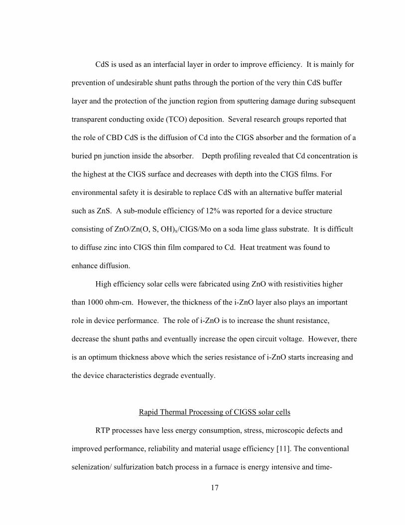
CdS is used as an interfacial layer in order to improve efficiency. It is mainly for
prevention of undesirable shunt paths through the portion of the very thin CdS buffer
layer and the protection of the junction region from sputtering damage during subsequent
transparent conducting oxide (TCO) deposition. Several research groups reported that
the role of CBD CdS is the diffusion of Cd into the CIGS absorber and the formation of a
buried pn junction inside the absorber. Depth profiling revealed that Cd concentration is
the highest at the CIGS surface and decreases with depth into the CIGS films. For
environmental safety it is desirable to replace CdS with an alternative buffer material
such as ZnS. A sub-module efficiency of 12% was reported for a device structure
consisting of ZnO/Zn(O, S, OH)x/CIGS/Mo on a soda lime glass substrate. It is difficult
to diffuse zinc into CIGS thin film compared to Cd. Heat treatment was found to
enhance diffusion.
High efficiency solar cells were fabricated using ZnO with resistivities higher
than 1000 ohm-cm. However, the thickness of the i-ZnO layer also plays an important
role in device performance. The role of i-ZnO is to increase the shunt resistance,
decrease the shunt paths and eventually increase the open circuit voltage. However, there
is an optimum thickness above which the series resistance of i-ZnO starts increasing and
the device characteristics degrade eventually.
Rapid Thermal Processing of CIGSS solar cells
RTP processes have less energy consumption, stress, microscopic defects and
improved performance, reliability and material usage efficiency [11]. The conventional
selenization/ sulfurization batch process in a furnace is energy intensive and time-
17
consuming. Large substrates can be processed in RTP systems without compromising
process uniformity or ramp rates because energy sources face the substrate. Thus the
process time cycle and energy budget can both be minimized, eliminating the bottlenecks
in CuIn1-xGaxSe2-ySy (CIGSS) module fabrication.
In a typical RTP system, the substrate is heated by two banks of linear lamps -
one above and one below it. The lamps are further subdivided into zones that can be
individually programmed with various powers to optimize temperature uniformity. A
variety of heating configurations, energy sources and temperature control methods can be
used. Arrangement of the lamp assembly system and the spectrum of incoherent light
sources determine the properties of processed material.
In the advanced stacked elemental process for CuIn1-xGaxSe2 (CIGS) thin-film
formation, the elemental precursor film is deposited by DC-magnetron sputtering of
CuGa and indium onto the Mo back contact. This is followed by thermal evaporation of
Se. For the absorber film formation, this precursor film is treated in a RTP furnace in a
sulfur-containing ambient in order to increase open circuit voltage (Voc) of the final cell.
The same basic process is used to fabricate CuInS2 modules [12].
18

CHAPTER THREE: SOFTWARE DEVELOPMENT FOR
AUTOMATION
Automation of deposition of Mo, CIG layers
Earlier depositions were carried out with the help of a chain and sprocket
mechanism that was operated manually by one person. The substrate would be moved
manually by ½” after a calculated amount of time for deposition of the precursor layer
(Mo or CuGa or In). As a result, one person would spend a considerable amount of time
in depositing the required layer. The resulting layer was found to have a thickness
variation of ±3% over the central 4” x 4” region and sheet resistance in the range of 1.9 –
2.1Ω/ [13].
Recently this mechanism was improved by attaching a substrate-holding frame to
the coupler which moved with the help of a threaded rod. The threaded rod, in turn was
coupled to an external stepper motor. The stepper motor was controlled by a LABVIEW
program that was developed in-house (Figure 8).
Figure 8: Photograph of PC running LABVIEW deposition program
19

The block diagram for the deposition control mechanism is shown in Figure 9:
Figure 9: Block diagram for deposition systems for CIG, Mo and ZnO/ZnO:Al
After successful installation of the first stepper motor for the DC magnetron
sputtering chamber, it was decided to use the same mechanism for the RF magnetron
sputtering chamber in which the ZnO and ZnO:Al layers are deposited. The same PC,
NI-DAQ card and feed-through block have been used for both chambers for cost
reduction.
The list of components for the stepper motor mechanism is given in Appendix B.
Siemens power supply, 24V, 5A
Stepper motor controller (drive)
Stepper motor
PC running LABVIEW
CIG Deposition chamber
RS-232 cable
SCXI-1302 feedthrough terminal block SH68-68-EP noise rejecting
cable
NI-DAQ card – 6024E
Siemens power supply, 24V, 5A
Stepper motor controller (drive) Stepper motor ZnO Deposition
chamber
20

Initially a small program with a simple user interface was written to control
stepper motor motion for the copper-indium-gallium (CIG) vacuum chamber (Figure 11).
The connections for this program are given in Table 1.
Table 1: Connections for CIG vacuum chamber (initial)
Pin Name
– NI
DAQ
card
Pin# (
terminal
block)
Stepper motor drive terminal RS-
232
pin#
Wire color
DIO0 25 STEP+ (input used to command motor
rotation)
1 Orange
DIO1 27 DIR+ (input that determines direction of
motor rotation)
2 Blue
DIO6 30 ENABLE+ (used to enable 6410’s power
stage)
3 Green
DIO2 29 STEP- (input to command motor rotation) 6 Brown
DIO3 31 DIR- (determines direction of motor
rotation)
7 Black
DIO5 28 ENABLE- (input to enable 6410’s power
stage)
8 Red
The digital input/output terminals of the DAQ card were being used to send
digital signals to the stepper motor. The STEP- was toggled between HIGH and LOW
states to send pulses to the stepper motor. One pulse to the STEP- terminal of the stepper
21

motor advanced it by one step. The connection diagram for the 6410 drive is shown in
Figure 10.
Figure 10: Connection diagram for stepper motor drive, power supply and stepper motor
The user interface for this program was as shown below:
Figure 11: User interface for stepper motor test program
The user could enter the time within which the substrate would move 0.5 inches.
The direction of motion could be switched to FORWARD or REVERSE. It was found
22
that the STEP- terminal could not be toggled fast enough when the DAQ digital port
connected to it was toggled. There was a limit to the frequency at which this digital
output port could be toggled. The connections were then changed. The frequency counter
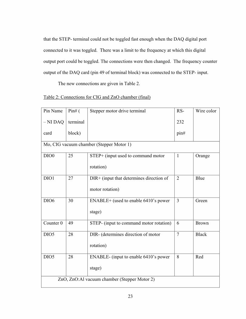
output of the DAQ card (pin 49 of terminal block) was connected to the STEP- input.
The new connections are given in Table 2.
Table 2: Connections for CIG and ZnO chamber (final)
Pin Name
– NI DAQ
card
Pin# (
terminal
block)
Stepper motor drive terminal RS-
232
pin#
Wire color
Mo, CIG vacuum chamber (Stepper Motor 1)
DIO0 25 STEP+ (input used to command motor
rotation)
1 Orange
DIO1 27 DIR+ (input that determines direction of
motor rotation)
2 Blue
DIO6 30 ENABLE+ (used to enable 6410’s power
stage)
3 Green
Counter 0 49 STEP- (input to command motor rotation) 6 Brown
DIO5 28 DIR- (determines direction of motor
rotation)
7 Black
DIO5 28 ENABLE- (input to enable 6410’s power
stage)
8 Red
ZnO, ZnO:Al vacuum chamber (Stepper Motor 2)
23

+5V 34 STEP+ 1 Orange
DIO3 31 DIR+ 2 Blue
DIO7 32 ENABLE+ 3 Green
Counter 1 43 STEP- 6 Brown
0V 33 DIR- 7 Black
0V 33 ENABLE- 8 Red
The block diagram for the program is shown in Figure 12.
Figure 12: Block diagram for stepper motor vi
Initially the digital I/O channels DIO0-DIO7 were configured with the
Measurement and Automation Explorer. All of them are digital output channels.
24

Figure 13: Generate Pulse Train vi (built-in LABVIEW vi)
The Generate Pulse Train vi (Figure 13) was used to configure Counter 0 with a
continuous pulse train output. The pulse polarity was kept ‘LOW’ ie. phase 1 is HIGH
and phase 2 is LOW. The duty cycle was chosen to be 50%. Frequency of the pulse train
was calculated dynamically depending on the user input for the number of seconds for ½”
movement of the substrate.
As soon as the user executed the program, the frequency of the pulse train would
be calculated as follows:
Frequency = steps per revolution of motor (400)/(2x speed (in sec/0.5”) x 0.0625)
A counter would output a pulse train of this frequency at pin #49. The motion of the
motor would stop when the ENABLE- terminal was switched to FALSE.
Though the required motor speed was achieved, the user was required to STOP
the program after the exact calculated time so that the substrate would not reach the end
of the chamber and knock against the wall of the vacuum chamber. It was thought that
the user interface of the program needed to be enhanced in order to do away with the
requirement of one person constantly monitoring the time left for the substrate to move
the required distance.
25

The program was updated and the user interface was changed to the one shown in
Figure 14 by Matthew Nugent.
Figure 14: User interface for enhanced LABVIEW program for CIG, Mo deposition
Depositions were divided into several passes. LEDS indicate which pass is
currently being processed. The block diagram for lighting LEDS according to the current
pass number is shown in Figure 15.
26
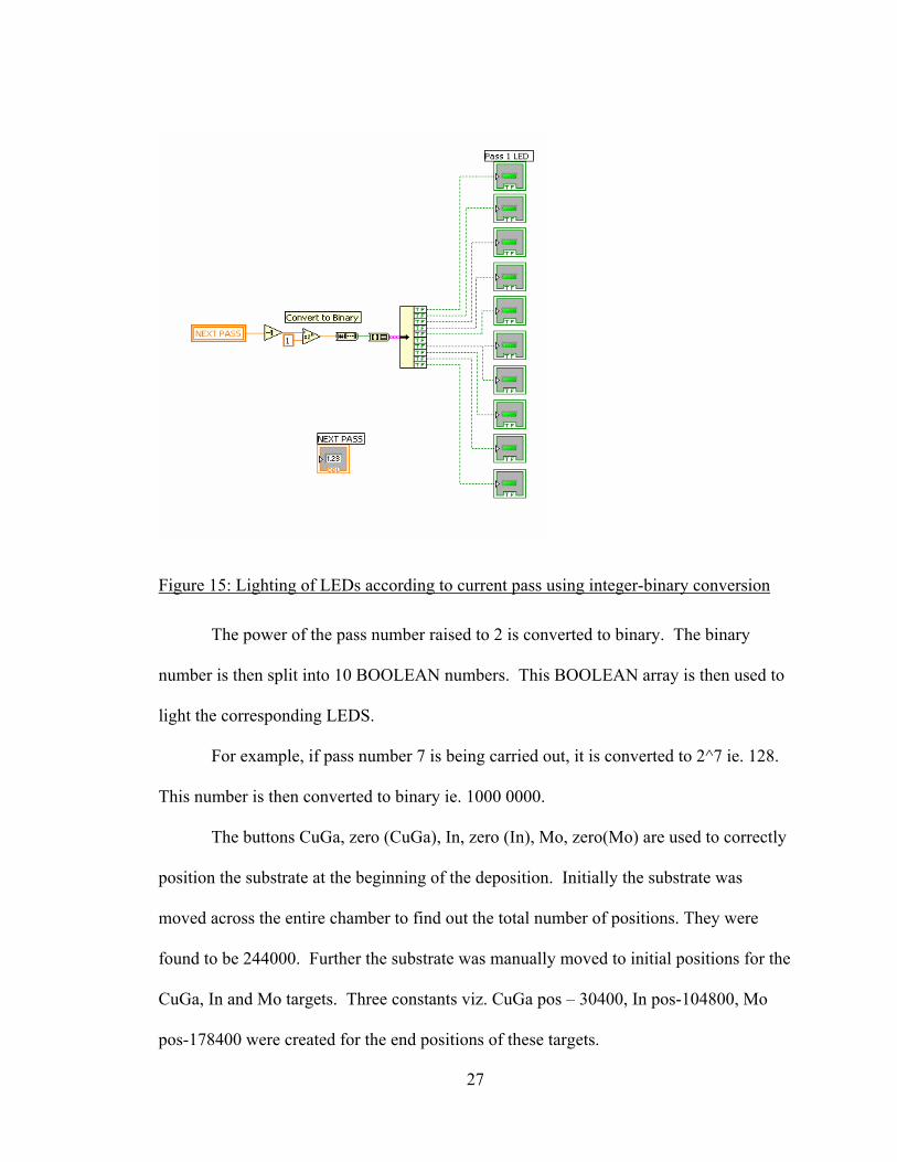
Figure 15: Lighting of LEDs according to current pass using integer-binary conversion
The power of the pass number raised to 2 is converted to binary. The binary
number is then split into 10 BOOLEAN numbers. This BOOLEAN array is then used to
light the corresponding LEDS.
For example, if pass number 7 is being carried out, it is converted to 2^7 ie. 128.
This number is then converted to binary ie. 1000 0000.
The buttons CuGa, zero (CuGa), In, zero (In), Mo, zero(Mo) are used to correctly
position the substrate at the beginning of the deposition. Initially the substrate was
moved across the entire chamber to find out the total number of positions. They were
found to be 244000. Further the substrate was manually moved to initial positions for the
CuGa, In and Mo targets. Three constants viz. CuGa pos – 30400, In pos-104800, Mo
pos-178400 were created for the end positions of these targets.
27
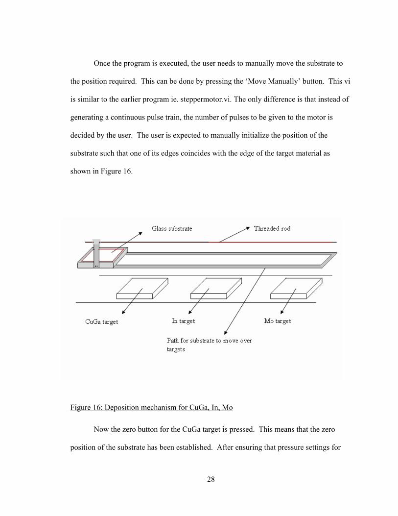
Once the program is executed, the user needs to manually move the substrate to
the position required. This can be done by pressing the ‘Move Manually’ button. This vi
is similar to the earlier program ie. steppermotor.vi. The only difference is that instead of
generating a continuous pulse train, the number of pulses to be given to the motor is
decided by the user. The user is expected to manually initialize the position of the
substrate such that one of its edges coincides with the edge of the target material as
shown in Figure 16.
Figure 16: Deposition mechanism for CuGa, In, Mo
Now the zero button for the CuGa target is pressed. This means that the zero
position of the substrate has been established. After ensuring that pressure settings for
28
the chamber have been done correctly and plasma can be seen, the user presses the RUN
button to begin CuGa deposition. This functionality has been implemented by
continuously finding the difference between the required end position and the current
position. Pulses are given to the stepper motor till the end position is reached.
After successful implementation of the deposition program for CuGa, In and Mo
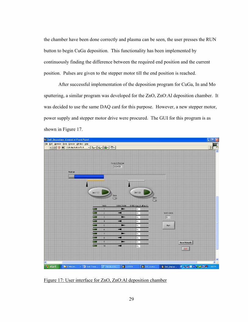
sputtering, a similar program was developed for the ZnO, ZnO:Al deposition chamber. It
was decided to use the same DAQ card for this purpose. However, a new stepper motor,
power supply and stepper motor drive were procured. The GUI for this program is as
shown in Figure 17.
Figure 17: User interface for ZnO, ZnO:Al deposition chamber
29

Depositions can be completed without any human supervision, thus saving
valuable time and energy.
30
Current-voltage (I-V) measurement setup using DAQ card
The earlier I-V measurement setup was developed using a data acquisition (NI-
DAQ) card, operational amplifier and micromanipulator probes. It was felt that these
measurements could be carried out automatically with the help of a LABVIEW program
for convenience and speed. This I-V measurement setup consisted of a simple circuit
interfaced to a PC with the help of a National Instrument data acquisition card. The block
diagram is as shown in Figure 18.
Terminal adapter
PCB with BUF04
Solar cell/ diode
NI SCXI-1302
+/- 12V Power supply
PC NI-DAQ: 6024E
Figure 18: Block Diagram for I-V measurement Setup
The BUF04 is a voltage buffer with high output current drive capability. It was
powered by a +/-12 Volt power supply. The output voltage of the BUF04 was given to
the solar cell/diode whose characteristics were to be measured. The current through the
solar cell/diode was measured by means of a 1 ohm resistor connected in series with it.
The BUF04 was driven by the analog output channel of the DAQ card. The voltage
31

across the solar cell/diode and that across the resistor was measured using two analog
input channels of the DAQ card (see Figure 19). These channels were created using the
Measurement and Automation Explorer provided by National Instruments.
From analog output channel of DAQ card (Vin)
+12V
Figure 19: Circuit Diagram for PCB with BUF04
A snapshot of the I-V measurement program is shown in Figure 20. The desired
range and step size were entered in the respective fields. The I-V plot was updated after
every single measurement. After the last measurement, the program prompted the user to
save this voltage and current data to an Excel sheet. Thus, the data could be saved for
later use.
1µF7
3BUF04
-12V
1 µF
64 A
To analog input channels of DAQ card
V 5kΩ
B
I
C
32

Figure 20: Snapshot of LABVIEW program for I-V measurement
Current-voltage (IV) measurement setup
The current flowing through a 0.47 cm2 solar cell is typically in the range of 0.01
mA. It was therefore thought that a high-accuracy power supply and multi-meter would
make the setup more reliable and robust.
Figure 21 shows a block diagram of the new, higher accuracy I-V setup.
33

Illumination Kepco Power Supply
Figure 21: I-V measurement setup
The BOP 20-5D power supply from Kepco is capable of supplying +/- 20V (0-
5A). Its output is connected to micromanipulator probes that are in contact with the solar
cell. The 6.5 digit 34401A multimeter from Agilent Technologies (0.0015% accuracy) is
connected in series with the solar cell to measure the resulting current. The power
supply and multimeter (both capable of GPIB communication) are connected to a
computer with an IEEE 488.2 card. The solar cell is kept in a wooden enclosure with a
lamp and cooling fan attached. The lamp power has been calibrated such that its
irradiance is 1000 W/m2. This was carried out with a pyranometer.
Before running the program, the solar cell is kept at the centre of the wooden
enclosure, the lamp is switched on and its intensity increased till it reaches 1000 W/m2.
The lamp is cooled with a fan. A snapshot of the I-V measurement program is shown in
Figure 22. The user can select one of two options ie. plot an I-V graph or display a stored
I-V graph.
Agilent Multimeter
GPIB cableComputer running LABVIEW
Solar cell
GPIB cable
34

Figure 22: Graphical User Interface for the I-V measurement program
If the user desires to plot an I-V graph (Figure 23), the desired range and step size
are entered in the respective fields. The program can now be run to step through the
required range. The I-V plot is updated after every single measurement. After the last
measurement, the program prompts the user to save this voltage, current and power data
to an Excel sheet. Thus, the data for each cell can be saved for later use.
35

Figure 23: Plotting I-V data
36

Figure 24: Retrieving dark and light I-V data
If the user desires to view details for the I-V characteristics of a previously tested
solar cell, he can choose the ‘Read I-V file’ option (Figure 24). The user just needs to
enter the cell area and run the program to retrieve detailed data ie. Voc, Isc, Jsc, Vmp, Imp,
fill factor and efficiency of the cell.
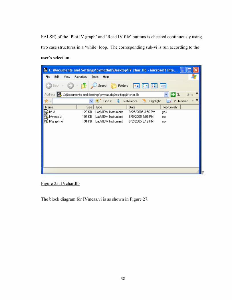
Description of the block diagram for IV.vi
When IVchar.llb is opened (FFigure 25), IV.vi is the top level vi (Figure 26)
(virtual instrument). Here, as soon as the program is run, the logical status (TRUE or
37
FALSE) of the ‘Plot IV graph’ and ‘Read IV file’ buttons is checked continuously using
two case structures in a ‘while’ loop. The corresponding sub-vi is run according to the
user’s selection.
F
Figure 25: IVchar.llb
The block diagram for IVmeas.vi is as shown in Figure 27.
38
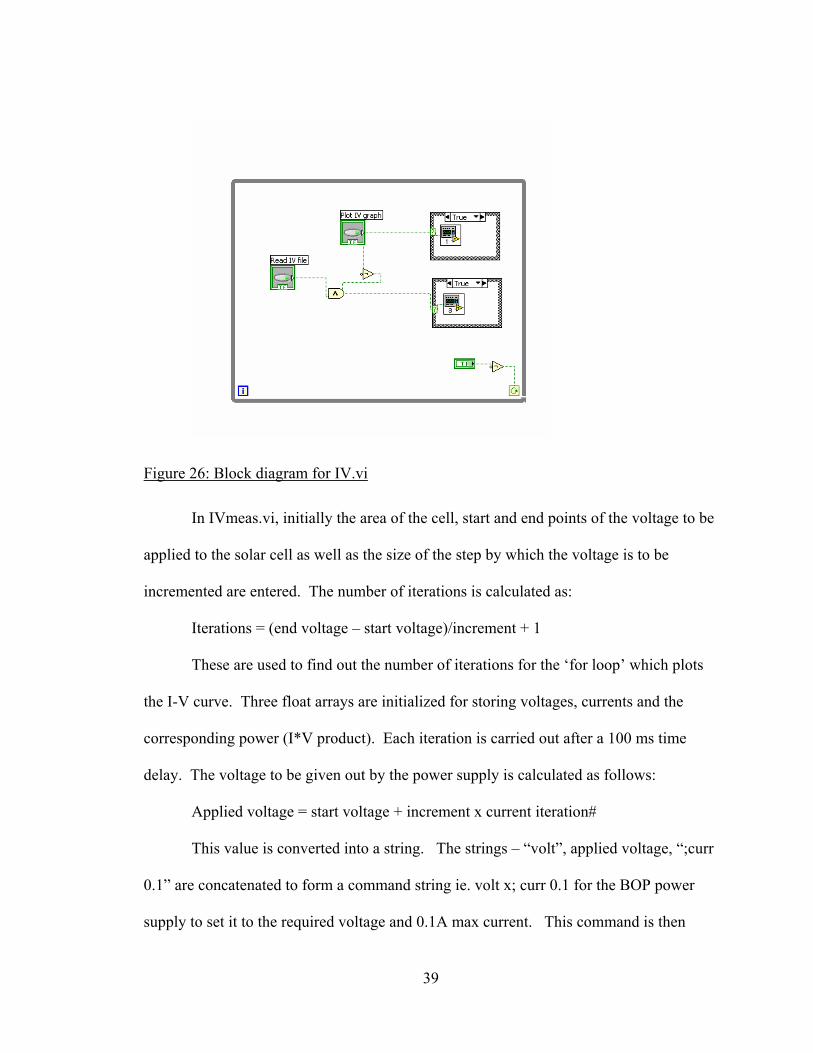
Figure 26: Block diagram for IV.vi
In IVmeas.vi, initially the area of the cell, start and end points of the voltage to be
applied to the solar cell as well as the size of the step by which the voltage is to be
incremented are entered. The number of iterations is calculated as:
Iterations = (end voltage – start voltage)/increment + 1
These are used to find out the number of iterations for the ‘for loop’ which plots
the I-V curve. Three float arrays are initialized for storing voltages, currents and the
corresponding power (I*V product). Each iteration is carried out after a 100 ms time
delay. The voltage to be given out by the power supply is calculated as follows:
Applied voltage = start voltage + increment x current iteration#
This value is converted into a string. The strings – “volt”, applied voltage, “;curr
0.1” are concatenated to form a command string ie. volt x; curr 0.1 for the BOP power
supply to set it to the required voltage and 0.1A max current. This command is then
39

given to the GPIB Write vi shown in Figure 28. The address of the power supply GPIB
instrument is 6.
In the same iteration, the current from the multimeter is measured. The command
string ‘meas:curr:dc?’ is given to this block using the GPIB Write vi. The measured
current is read with the help of the GPIB Read vi (Figure 29). The address of the
multimeter GPIB instrument is 22. A byte count of 200 is given for the buffer in which
the reading is stored.
Following this, the current, voltage and power are appended to their respective
arrays using the ‘Insert into Array’ block. The voltage-current and voltage-power arrays
are bundled together and two separate arrays are built again for plotting the I-V
characteristics as well as the power curve on the same plot.
After all iterations are completed, the user can save them in a text file for future
reference. Further, Voc is located by looking for the index of the smallest absolute value
of current (close to 0). Isc is located by looking for the index of the smallest absolute
value of voltage. The maximum power point is calculated by searching for the index
with the highest absolute power value. The corresponding voltage and current values are
the Vmp and Imp respectively.
40

Figure 27: Block diagram of IVmeas.vi
Figure 28: GPIB write
41

Figure 29: GPIB read
The fill factor of the cell is calculated as:
scoc
mpmp
I V)I (V factor Fill =
Efficiency is calculated as:
Irradiancex area Cell)I(V Efficiency mpmp
=
If the user chooses to retrieve a file, the IVgraph.vi is opened. The block diagram
of IVgraph.vi is shown in Figure 30.
In this vi, all arrays are retrieved from the saved file. The user needs to enter the
area of the cell. The Voc, Isc, Vmp, Imp, fill factor and efficiency are computed similar to
IVmeas.vi.
42
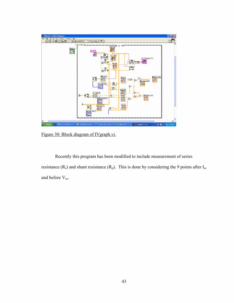
Figure 30: Block diagram of IVgraph.vi.
Recently this program has been modified to include measurement of series
resistance (Rs) and shunt resistance (Rp). This is done by considering the 9 points after Isc
and before Voc.
43
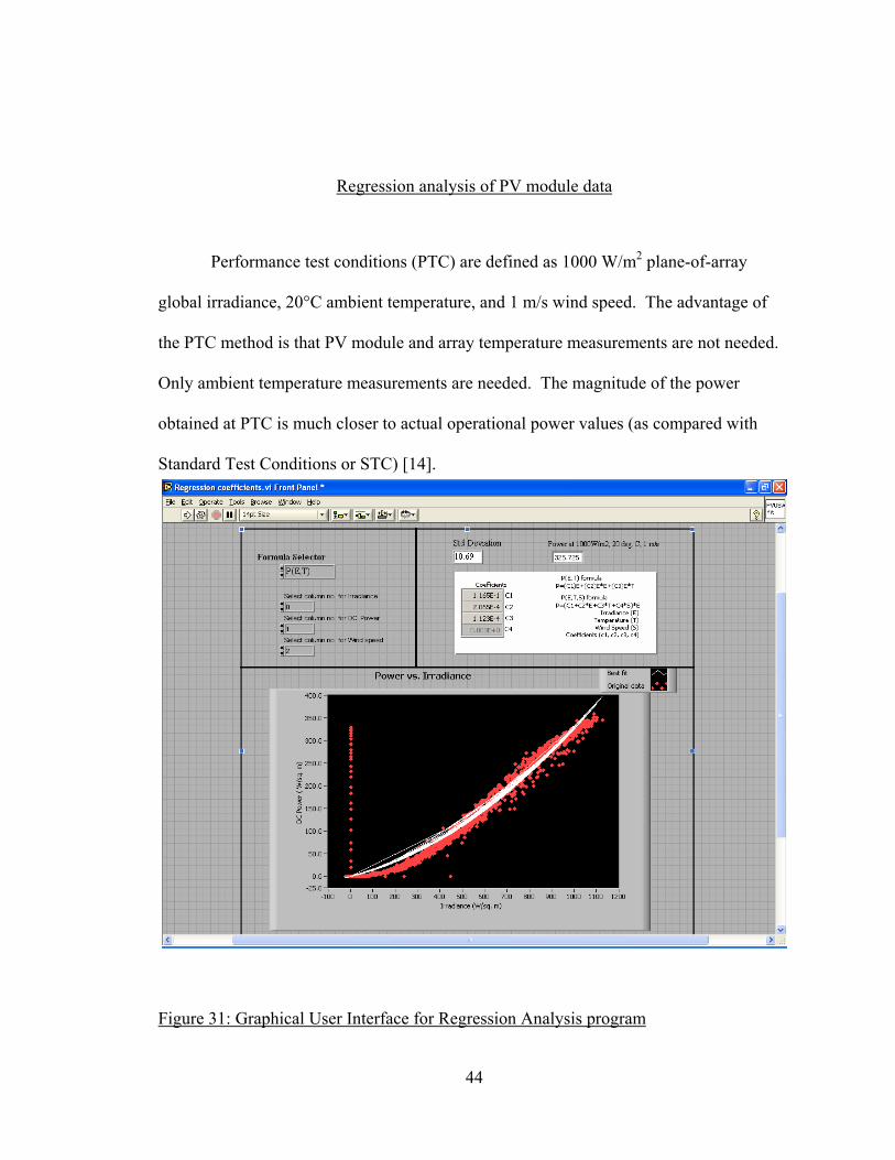
Regression analysis of PV module data
Performance test conditions (PTC) are defined as 1000 W/m2 plane-of-array
global irradiance, 20°C ambient temperature, and 1 m/s wind speed. The advantage of
the PTC method is that PV module and array temperature measurements are not needed.
Only ambient temperature measurements are needed. The magnitude of the power
obtained at PTC is much closer to actual operational power values (as compared with
Standard Test Conditions or STC) [14].
Figure 31: Graphical User Interface for Regression Analysis program
44

Performance degradation of test modules can be detected with the help of PTC
regressions. Daily data for PV module arrays at the FSEC test site is available online to
authorized users in the form of a .dat file and consists of irradiance, DC power, ambient
temperature and wind speed besides other parameters such as relative humidity,
ultraviolet radiation, module temperature, reference temperature etc. Before executing
the program, the user enters the column nos. for Irradiance(E), DC power(P), ambient
temperature(T) and wind speed(S). When ‘Regression coefficients.vi’ is executed, the
program asks the user to select a .dat file for analysis. The program then plots a graph of
Power vs. Irradiance. It tries to find a best fit equation for the DC power and computes 3
temperature coefficients by considering Irradiance and ambient temperature if the
formula P(E, T) is selected ie. P=(C1)E+(C2)E*E+(C3)E*T. Similarly, it computes 4
temperature coefficients by considering irradiance, ambient temperature and wind speed
if the formula P(E, T, S) is selected ie. P=(C1+C2*E+C3*T+C4*S)*E.
The coefficients are then substituted into the formula:
P=(C1+C2*E+C3*T+C4*S)*E with E = 1000 W/m2, T = 20°C and S = 1m/s to find out
the PTC power value for the given period (usually 1 month). The user is given the option
to save the temperature coefficients ie. C1, C2, C3 and C4 along with the computed PTC
power value in a .dat file for reference. The PTC power values for each month of the
year are then plotted to find out the degradation rate of each module array over time.
The block diagram for ‘Regression coefficients.vi’ is shown in Figure 32.
Initially the user enters the name of the .dat file to be read. This is implemented using the
‘Read from Spreadsheet File. vi’. All columns of the file are read into an array. The
required sub-arrays i.e. DC Power, Irradiance, Ambient Temperature and Wind Speed are
45
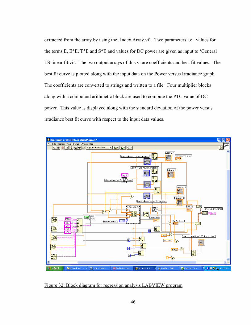
extracted from the array by using the ‘Index Array.vi’. Two parameters i.e. values for
the terms E, E*E, T*E and S*E and values for DC power are given as input to ‘General
LS linear fit.vi’. The two output arrays of this vi are coefficients and best fit values. The
best fit curve is plotted along with the input data on the Power versus Irradiance graph.
The coefficients are converted to strings and written to a file. Four multiplier blocks
along with a compound arithmetic block are used to compute the PTC value of DC
power. This value is displayed along with the standard deviation of the power versus
irradiance best fit curve with respect to the input data values.
Figure 32: Block diagram for regression analysis LABVIEW program
46
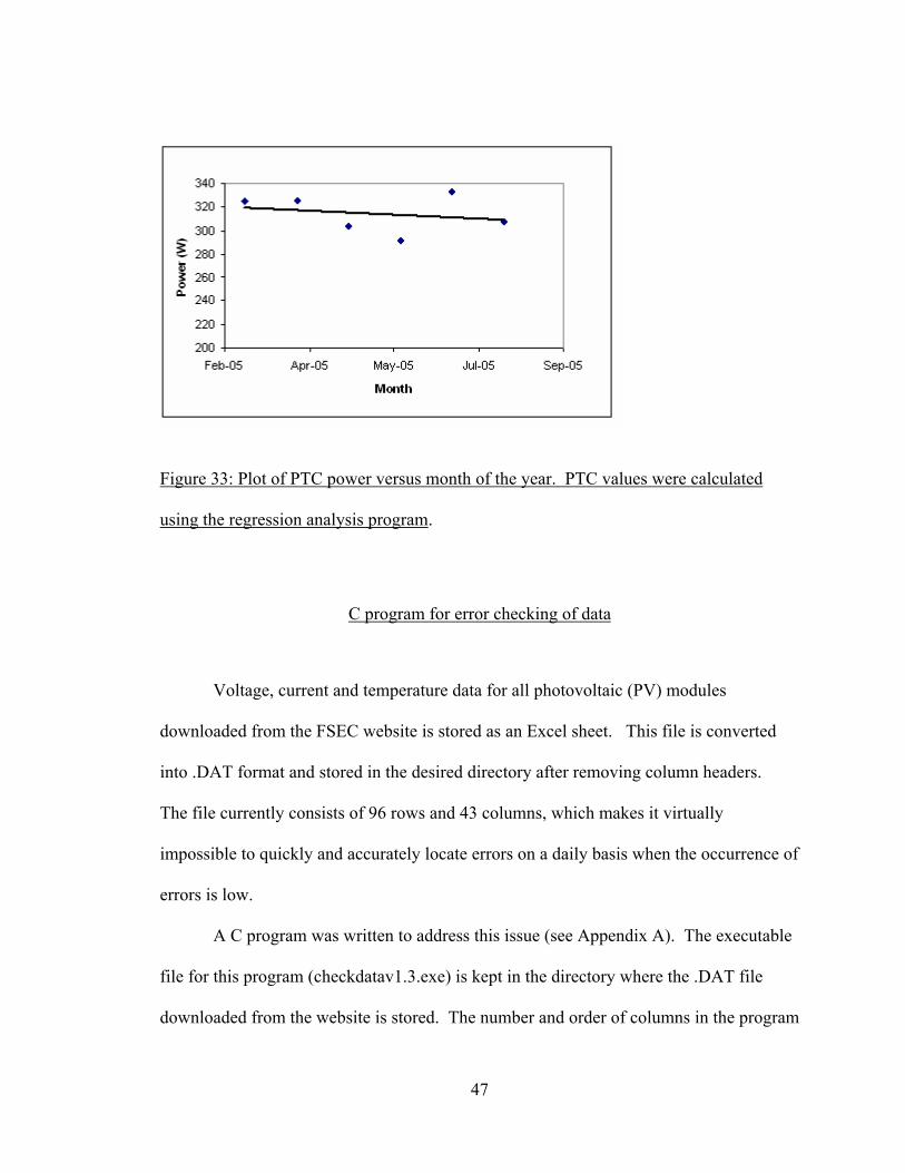
Figure 33: Plot of PTC power versus month of the year. PTC values were calculated
using the regression analysis program.
C program for error checking of data
Voltage, current and temperature data for all photovoltaic (PV) modules
downloaded from the FSEC website is stored as an Excel sheet. This file is converted
into .DAT format and stored in the desired directory after removing column headers.
The file currently consists of 96 rows and 43 columns, which makes it virtually
impossible to quickly and accurately locate errors on a daily basis when the occurrence of
errors is low.
A C program was written to address this issue (see Appendix A). The executable
file for this program (checkdatav1.3.exe) is kept in the directory where the .DAT file
downloaded from the website is stored. The number and order of columns in the program
47

is fixed. The program would have to be modified if any un-installation of existing
modules/installation of new modules is carried out.
On execution, the program prompts the user to enter the filename and number of
rows as shown in Figure 34. The program checks the following:
1. All data lies within the normal, expected range 2. Voltage and current signs are correct for positive and negative arrays
3. If there is a large difference in current and voltage values for positive and
negative arrays of the same manufacturer, under the same ambient conditions
The program is executed within 1 second and errors in data are logged in a text
file. The row and column numbers are pointed out in the log file in order to facilitate
further troubleshooting. Thus, valuable time is saved and usual types of errors are
detected.
Figure 34: Execution of error-checking program for downloaded .DAT file
48

CHAPTER FOUR: CONSTRUCTION OF SETUPS – RTP and QE
Rapid Thermal Processing Unit
A Rapid Thermal Processing (RTP) unit has been designed, constructed and
installed for preparation of CIGSS thin films on 10 cm x 10 cm substrates by
selenization/ sulfurization of elemental precursors using the vacuum deposited selenium
layer and N2:H2S atmosphere. The schematic is shown in Figure 35.
Figure 35: Schematic of RTP setup
A quartz tube (ID = 15 cm) is mounted with a stainless steel flange assembly. A
pair of high density infrared heaters (Research Inc., Model 5090), each with a bank of 5
T3-style quartz infrared halogen lamps directs energy onto the reaction tube where the
Sliding wheel To mechanical pump
Flange assembly
Infrared Heater with electrical and water connections
Gas
Lid
Array of 5 Tungsten Halogen Lamps
Reaction Tube (Quartz)
Thermocouple
Substrate to be processed
Exhaust Valve
Mobile mounting frame
49
substrate is kept. Each lamp is rated at 1200 Watts and power to the lamps is controlled
by a pair of single-phase (120V AC, 55 A) standalone SCR power controls (Research
Inc., Model 5620).
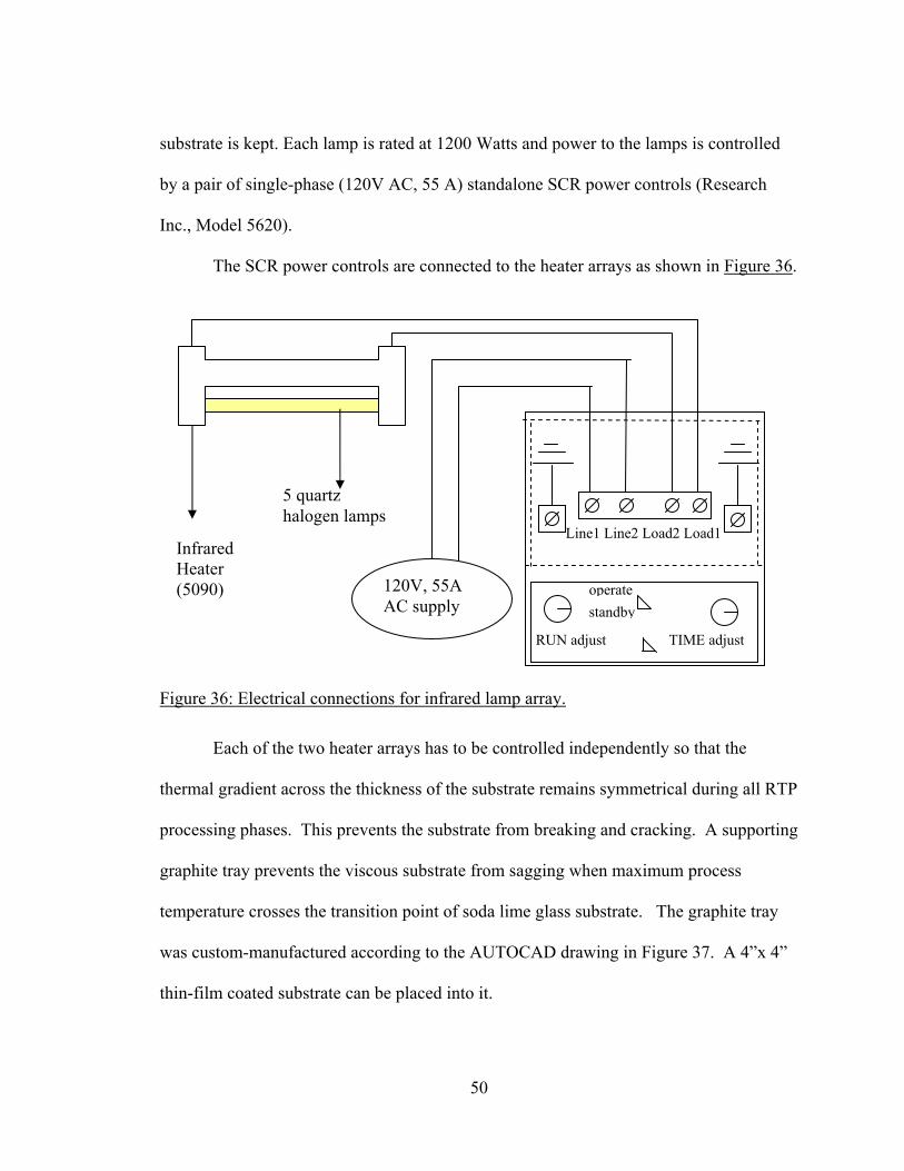
The SCR power controls are connected to the heater arrays as shown in Figure 36.
Figure 36: Electrical connections for infrared lamp array.
Each of the two heater arrays has to be controlled independently so that the
thermal gradient across the thickness of the substrate remains symmetrical during all RTP
processing phases. This prevents the substrate from breaking and cracking. A supporting
graphite tray prevents the viscous substrate from sagging when maximum process
temperature crosses the transition point of soda lime glass substrate. The graphite tray
was custom-manufactured according to the AUTOCAD drawing in Figure 37. A 4”x 4”
thin-film coated substrate can be placed into it.
Line1 Line2 Load2 Load1
5 quartz halogen lamps
Infrared Heater (5090) 120V, 55A
AC supply operatestandby
RUN adjust TIME adjust
50
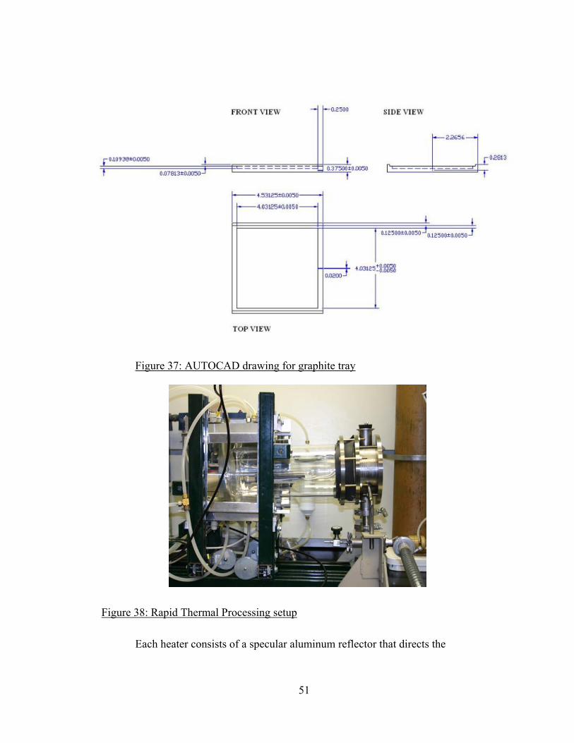
Figure 37: AUTOCAD drawing for graphite tray
Figure 38: Rapid Thermal Processing setup
Each heater consists of a specular aluminum reflector that directs the
51

infrared energy supplied by the lamps on to the substrate. Connections to supply required
cooling water to the heater are provided. A sliding mechanism has been provided to
quickly move the heaters away from the quartz tube after the completion of the process
for rapid cooling.
Quantum Efficiency measurement setup
The basis of the quantum efficiency (QE) setup was made from a wooden
enclosure with removable top fixed to a metal breadboard. The interior components were
mounted on the breadboard as shown in the block diagram (Figure 39). The tungsten-
halogen lamp was connected to a 12V DC Kepco power supply. A cooling fan was
installed within the enclosure for cooling the lamp. A monochromator was kept in the
path of the light rays emanating from this lamp. A light chopper (with frequency set to
100 Hz) and a filter wheel with one long pass filter (>500 nm) were arranged in sequence
after the monochromator. After obtaining the focus point for the beam of light, it was
reflected with the help of a mirror onto a beam splitter. The beam splitter transmits 75 %
of the incident light. Reflected and reference light is converted into an electric current in
the µA range using photo-detectors. These AC signals have a frequency of 100 Hz.
They are amplified by connecting them to a current preamplifier followed by a lock-in
amplifier. The lock-in amplifier is locked to the chopper frequency by connecting the
chopper frequency output to the reference input of the lock-in amplifier. The two current
preamplifiers and the three lock-in amplifiers are interfaced to the computer with the help
of 2 RS-232 cables and 3 GPIB cables respectively. The ‘Quantum Efficiency
52

measurement’ LABVIEW program was procured from NREL and was further modified
at FSEC as per the specific requirements.
When the program is executed, the user is asked to select a calibration file for
beam splitter transmittance. The user interface of the program is shown in Figure 40.
The flowchart for the QE measurement program is given in Figure 42.
After construction, the beam splitter transmittance curve was recalibrated for the
particular setup. Tests were carried out with the reference solar cell (whose QE values
were measured at NREL). Further testing of the standard cell produced a QE curve that
matched the reference curve as shown in Figure 41. Generally the measured curve is
within ±0.5% of the reference curve except for two peaks that show a deviation closer to
1%.
53
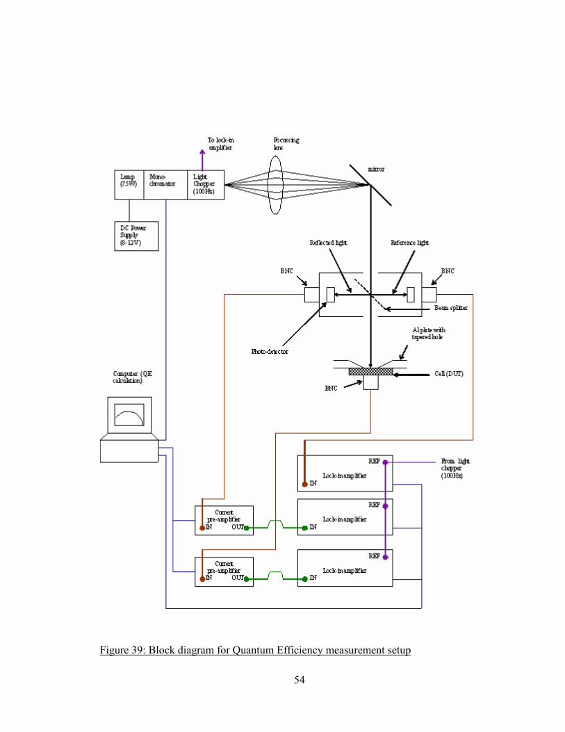
Figure 39: Block diagram for Quantum Efficiency measurement setup
54

Figure 40: GUI of QE measurement vi
0
10
20
30
40
50
60
70
400 450 500 550 600 650 700 750 800 850 900 950 1000
Wavelength (nm)
QE
(%)
Reference Curve
Measured Curve
Figure 41: Plot of QE vs wavelength
55

START
Initialize all variables and arrays, calculate number of points to be plotted
Read calibration file selected by user into global array variables
Establish communication with all devices, reset devices
Calculate quantum efficiency at current wavelength as
QE = [(1-BST)/BST]*calibrated QE*(test signal/reference
signal)/back cell QE
Increment wavelength of monochromator, plot QE vs. wavelength
No End wavelength reached?
Yes
Save QE values to a file along with the wavelengths
END
Figure 42: Flowchart for Quantum Efficiency measurement LABVIEW program
56

CHAPTER FIVE: EXPERIMENTAL TECHNIQUE
Fabrication process for CIGSS solar cells
Thin-film solar cell fabrication was initially carried out on 1.5”x1” solar cells at
FSEC. In 2002, 4” x 4” solar cell fabrication was initiated for space power applications.
The process for fabricating solar cells is as shown in the flowchart in Figure 43.
Deposition of precursor film by DC magnetron sputtering of CuGa, In on Mo back electrode
Thermal evaporation of NaF and Se
Heat treatment of film in conventional/RTP furnace
Chemical bath deposition of CdS layer
Etching of Cu-rich layer
Deposition of ZnO/ZnO:Al to form a transparent conducting front l
Ni-Al contact formation using e-beam evaporation
Figure 43: CIGSS solar cell fabrication process
57

Substrate preparation
Soda lime glass pieces which are used for solar cell preparation are stored in a
vacuum sealed chamber to prevent contamination. A 6” x 4” piece of Mo-coated (specify
thickness etc) soda lime glass was cut from a large sheet. The glass piece was held under
running tap water. A 50/50 solution of soap and water was used to scrub the surface.
Tap water was used to clean the surface. This was followed by thorough rinsing of the
surface with distilled, de-ionized water. Isopropanol was used to dissolve impurities.
The substrate was thoroughly rinsed with de-ionized water and finally blow-dried with a
jet of compressed Nitrogen gas.
Deposition of CuGa and In layers
Sputtering is a process in which material is dislodged and ejected from the surface
of a solid or liquid due to the surface bombardment by energetic particles. The source of
coating material (target) is placed in a vacuum chamber along with the substrates and
pressure of 10-4 to 10-7 Torr is obtained by evacuating the chamber. The bombarding
species are usually ions of a heavy inert gas eg. Argon. Substrates intercept the flux of
sputtered atoms as they are placed in front of the target (cathode). The chamber is filled
with upto 100 mTorr of the inert gas which is then ionized by applying potentials
between the target and anode range from 500-5000 V (Figure 44).
58

Figure 44: Principle of deposition by sputtering
A rectangular chamber of size ~38.5” x 18.5” x 6” has been built for deposition
from three metal targets (Molybdenum, Indium and CuGa) of size 12” x 4”. A rough
vacuum in the range of 10-2 Torr was obtained using a two-stage mechanical pump. A
cryopump was used to get vacuum up to 10-6 Torr. The optimum parameters for CuGa
and In deposition have already been determined [5].
Thermal evaporation of NaF and Se
A minute quantity of NaF (to improve grain size) and sufficient amount of Se
were evaporated over the CuGa/In bilayer in a vacuum chamber. High vacuum in the
range of <10-6 Torr was obtained in this vacuum system with a diffusion pump. The
system has been fitted with electrodes and holders for vacuum evaporation using a power
supply (5-10 V, 600 A). A liquid nitrogen trap prevents back streaming of diffusion
59

pump oil vapor to the substrates and minimizes the amount of Se vapor reaching and
damaging the pumps. The heater was enclosed in a quartz tube to prevent the spread of
Se vapor to other regions of the chamber (Figure 45).
Figure 45: Thermal evaporation setup
According to the cosine law of emission the mass deposited per unit area is given
by:
2
2
)(
coscos),(
rM
dAthicknessd
rM
dAdM
e
r
e
r
r
×=
××
=
ρπ
πθϕθϕ
where r is the distance between substrate surface and boat
ρ is the density of selenium
θ is the angle of incidence
φ is the angle of the normal to the surface element dAe
60

The amount of NaF and Se to be evaporated for the required thickness was
calculated using the above formula. The boats containing NaF and Se were heated
sequentially by slowly increasing the current to the electrodes (Figure 46, 47).
Figure 46: Before Se evaporation Figure 47: After Se evaporation
61

Heat treatment of the precursor film
The precursor film can be heat treated either in a conventional furnace or in the
recently built rapid thermal processing (RTP) setup:
Conventional furnace
The furnace is purged with 50 Torr hydrogen/nitrogen gas in 4 cycles. The
chamber is filled with 1% diethylselenide + H2 for selenization or 8% H2S + H2 for
sulfurization using mass flow controllers. The temperature of the furnace is then ramped
at a rate of 6°C/min till it reaches the desired temperature (475 °C). The pressure
reaches ~600 Torr at the end of the ramp. A dwell of 30 minutes is then provided to
promote complete intermixing of metallic precursors. After this, a temperature ramp and
dwell is programmed so as to facilitate sulfur incorporation and growth of CIGSS film.
At the end of the dwell, the furnace is allowed to cool to room temperature.
RTP furnace
In order to carry out heat treatment of the film in the RTP furnace, the lid of the
quartz tube is removed; the film-coated substrate is kept in the graphite tray. The
thermocouple is kept underneath the graphite tray to constantly monitor temperature.
The lid is now placed back and the infrared heaters are moved over the substrate. After
switching on the water supply and vacuum gauges, power to the infrared heaters is
switched ON. Power is adjusted to a predetermined value to achieve the desired ramp
62

rate. The power knob is then slowly turned down to make the substrate temperature
dwell at a fixed value. The heaters are moved away from the quartz tube for quick
cooling and the film is taken out of the graphite tray as soon as it reaches room
temperature.
The sheet resistance of the film is then measured using the two-probe method. A
low sheet resistance, in the range of < 500 Ω/ indicates a sufficiently Cu-rich film (n-
type). A sheet resistance in the range of > 1500 Ω/ indicates a Cu-poor film. This film
may then be immediately sent for analysis to find out the actual composition and
morphology or further processed to complete preparation of CIGSS thin-film solar cells.
Material characterization of the CIGSS thin films is carried out by scanning electron
microscopy (SEM) and composition is determined by means of X-ray energy dispersive
spectroscopy (XEDS).
Chemical bath deposition of CdS layer
Sulfurization of metallic precursors results in formation of copper rich Cu2-xS
(covellite) layer at the surface. This film is first etched with 10% KCN solution for about
5 minutes. It is then oxidized using hydrogen peroxide for about 3 minutes. The etched
and oxidized film is then transferred to a freshly prepared chemical bath deposition
(CBD) setup.
The CBD setup consists of a hot water bath, 1 litre beaker holding the reaction
solution, a sample holder and thermometers for monitoring the water bath and reaction
63

solution temperatures. The sample holder is designed to hold six samples at a time
(Figure 48).
Figure 48: Chemical bath deposition of CdS layer
The reaction solution (total 2074.5 ml) is made of:
1) Distilled deionized water – 1440 ml
2) NH4OH – 337.5 ml
3) 0.015M CdSO4 – 198 ml
4) 1.5M Thiourea – 99 ml
The reaction solution (with no thiourea) is added to the 1 litre beaker. The
samples with etched CIGSS film are loaded vertically along the wall of the beaker. The
samples are placed in the 1 litre beaker containing the reaction solution. This beaker is
64

placed in the hot water bath maintained at 85 °C. Thiourea is added to the reaction
solution – the temperature is recorded after every minute. The solution is clear at the
beginning of the experiment but turns light greenish yellow after 6-7 minutes and yellow
after 15 minutes. The samples are then removed and cleaned with distilled deionized
water. They are dried with compressed nitrogen jet. The color of the samples indicates
the thickness of CdS layer deposited.
Deposition of transparent conducting ZnO/ZnO:Al window bilayer
A vacuum chamber of size 29” x 8.5” x 6” has been fabricated for the deposition
of ZnO/ZnO:Al. It has two 4” x 12” magnetron sputtering sources installed for RF
magnetron sputtering from ZnO and ZnO:Al targets. Parameters for depositing ZnO are
typically: Power: 200 W, Pressure:1.5 mT. The speed of the substrate with respect to the
target is adjusted according to the thickness required. The thickness of the film can be
optimized by depositing a film on clean glass at a particular power, pressure and
deposition speed. Thickness is measured with a DEKTAK profilometer and
transmittance with a transmittance spectroscope. The sheet resistance of the ZnO film is
generally in the range of 50Ω/.
Deposition of Ni/Al contact fingers
E-beam evaporation works on the principle that when a current is passed
through a tungsten filament, thermionic emission of electrons takes place. Electrons are
65

focused towards the evaporant by means of permanent magnets and accelerated with a
voltage upto 10 kV. When the electron beam impinges on the surface of the evaporant,
the kinetic energy of its motion is transformed into heat. This causes the material to melt
and evaporate. A pattern of front contact grid is obtained with the help of a mechanical
mask placed on the substrate.
Nickel/Aluminium
Figure 49: Layer sequence of CIGSS thin-film solar cells
Scribing and soldering of In ribbons
In order to measure the I-V characteristics, it is necessary to have a back contact
in addition to the front contact i.e. Ni/Al fingers. This is done by removing the thin film
to expose the molybdenum layer. Indium is then spread out and soldered to this layer in
order to provide contact to the p-type CIS. Individual cells of size ~0.44 cm2 are then
isolated from each other by scribing the surrounding area (Figure 50).
n-type ZnO/ZnO:Al
n-type CdS
Selenize/Sulfurize p-type CIGS
Molybdenum
Glass
66
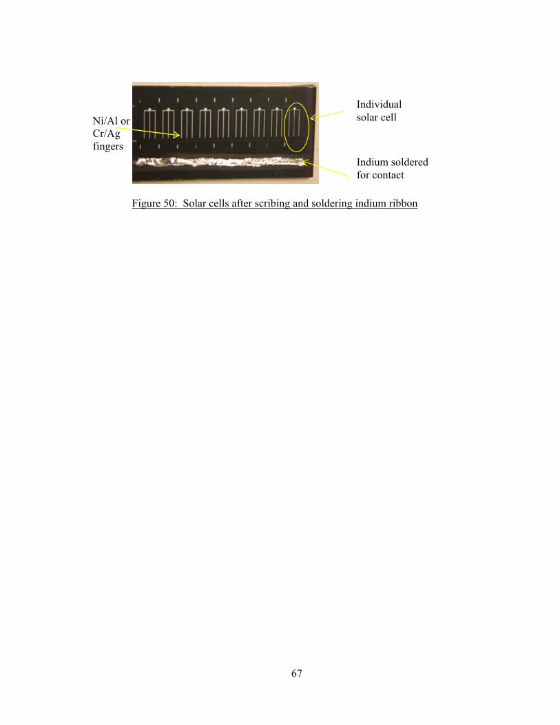
Ni/Al or Cr/Ag fingers
Individual solar cell
Indium soldered for contact
Figure 50: Solar cells after scribing and soldering indium ribbon
67
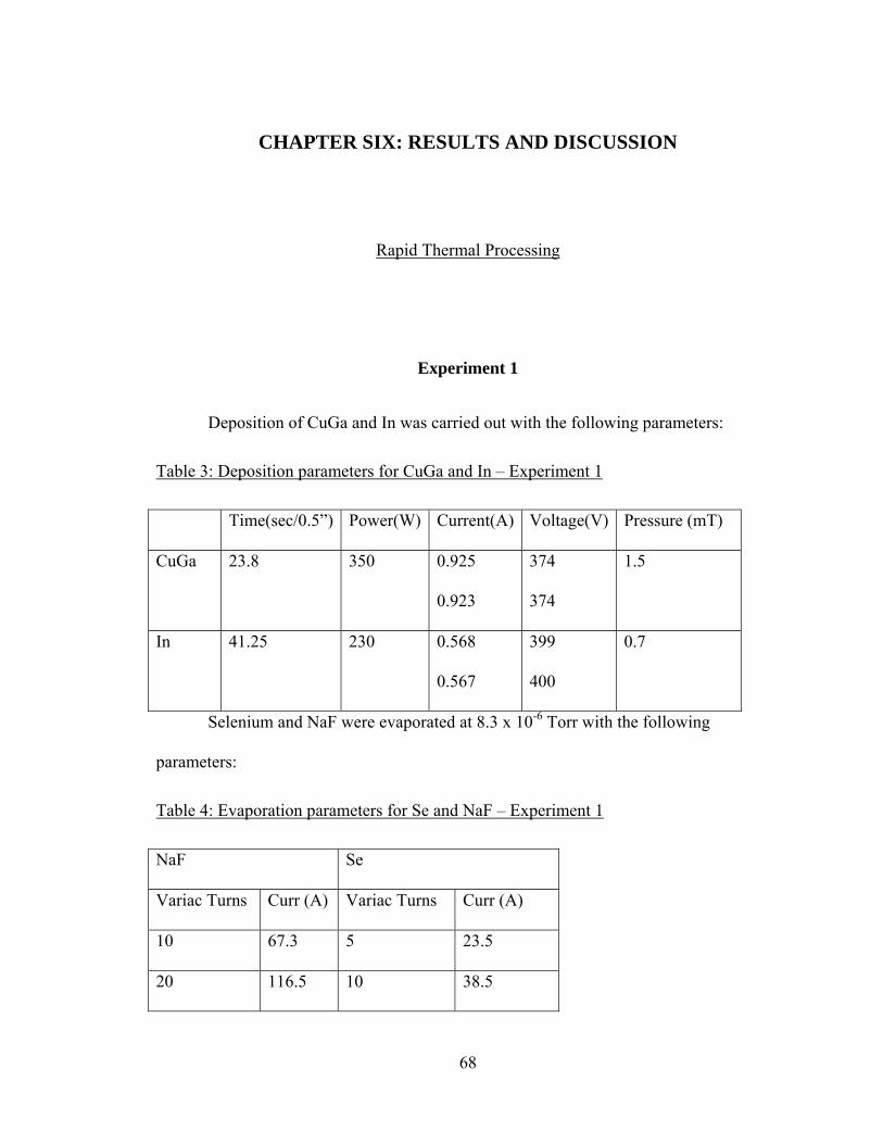
CHAPTER SIX: RESULTS AND DISCUSSION
Rapid Thermal Processing
Experiment 1
Deposition of CuGa and In was carried out with the following parameters:
Table 3: Deposition parameters for CuGa and In – Experiment 1
Time(sec/0.5”) Power(W) Current(A) Voltage(V) Pressure (mT)
CuGa 23.8
350 0.925
0.923
374
374
1.5
In 41.25 230 0.568
0.567
399
400
0.7
Selenium and NaF were evaporated at 8.3 x 10⁻⁶ Torr with the following
parameters:
Table 4: Evaporation parameters for Se and NaF – Experiment 1
NaF Se
Variac Turns Curr (A) Variac Turns Curr (A)
10 67.3 5 23.5
20 116.5 10 38.5
68
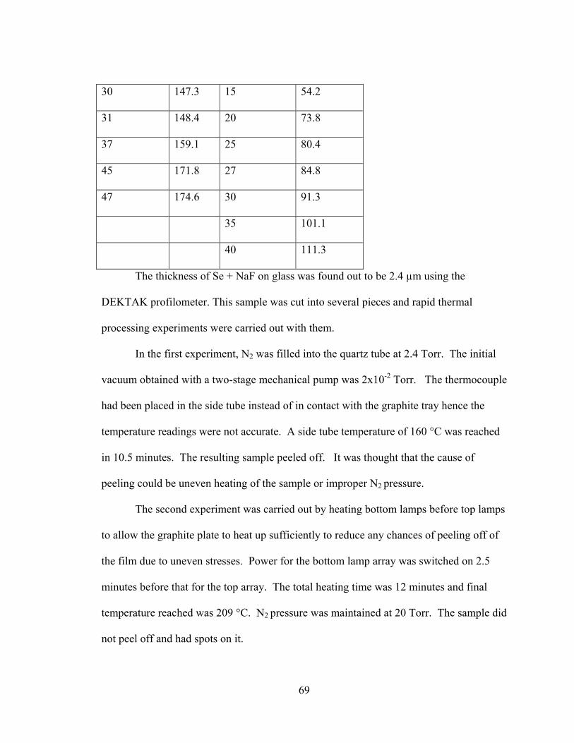
30 147.3 15 54.2
31 148.4 20 73.8
37 159.1 25 80.4
45 171.8 27 84.8
47 174.6 30 91.3
35 101.1
40 111.3
The thickness of Se + NaF on glass was found out to be 2.4 µm using the
DEKTAK profilometer. This sample was cut into several pieces and rapid thermal
processing experiments were carried out with them.
In the first experiment, N2 was filled into the quartz tube at 2.4 Torr. The initial
vacuum obtained with a two-stage mechanical pump was 2x10⁻² Torr. The thermocouple
had been placed in the side tube instead of in contact with the graphite tray hence the
temperature readings were not accurate. A side tube temperature of 160 °C was reached
in 10.5 minutes. The resulting sample peeled off. It was thought that the cause of
peeling could be uneven heating of the sample or improper N2 pressure.
The second experiment was carried out by heating bottom lamps before top lamps
to allow the graphite plate to heat up sufficiently to reduce any chances of peeling off of
the film due to uneven stresses. Power for the bottom lamp array was switched on 2.5
minutes before that for the top array. The total heating time was 12 minutes and final
temperature reached was 209 °C. N2 pressure was maintained at 20 Torr. The sample did
not peel off and had spots on it.
69

For the third piece, a N2 pressure of 24 Torr was maintained. A temperature of
365 °C was reached in 6 minutes. Heating was carried out for 10.5 minutes.
Temperature could not be measured further as the thermocouple connection was loose.
70

Experiment 2
Deposition of CuGa and In was carried out with the following parameters:
Table 5: Deposition parameters for CuGa and In – Experiment 2
Time(sec/0.5”) Power (W) Voltage (V) Current (A) Pressure (mT)
CuGa 27 350 371
372
0.932
0.93
1.5
In 41.25 230 400
402
0.568
0.563
0.7
Thermal evaporation of Se and NaF was carried out as follows:
Table 6: Evaporation parameters for Se and NaF – Experiment 2
NaF Se
Variac turns Current (A) Variac turns Current (A)
10 71.5 20 73.6
20 121.3 25 80.6
30 159.6 27 83.6
35 164.3 30 86.4
40 169.3 35 95.1
45 169.7 40 99.3
During the first RTP run, no nitrogen was filled in (vacuum), temperature was
ramped to 550°C and maintained at the same level for 6 minutes. The sample showed
71
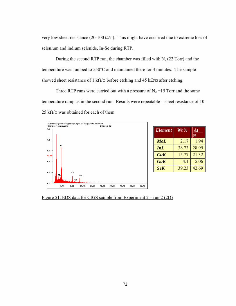
very low sheet resistance (20-100 Ω/). This might have occurred due to extreme loss of
selenium and indium selenide, In2Se during RTP.
During the second RTP run, the chamber was filled with N2 (22 Torr) and the
temperature was ramped to 550°C and maintained there for 4 minutes. The sample
showed sheet resistance of 1 kΩ/ before etching and 45 kΩ/ after etching.
Three RTP runs were carried out with a pressure of N2 =15 Torr and the same
temperature ramp as in the second run. Results were repeatable – sheet resistance of 10-
25 kΩ/ was obtained for each of them.
X
Element Wt % At
% MoL 2.17 1.94 InL 38.73 28.99 CuK 15.77 21.32 GaK 4.1 5.06 SeK 39.23 42.69
Figure 51: EDS data for CIGS sample from Experiment 2 – run 2 (2D)
72
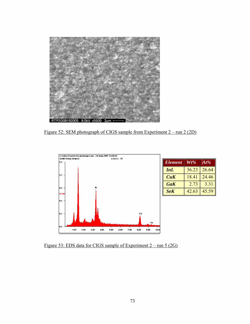
Figure 52: SEM photograph of CIGS sample from Experiment 2 – run 2 (2D)
Element Wt% At% InL 36.23 26.64 CuK 18.41 24.46 GaK 2.73 3.31 SeK 42.63 45.59
Figure 53: EDS data for CIGS sample of Experiment 2 – run 5 (2G)
73
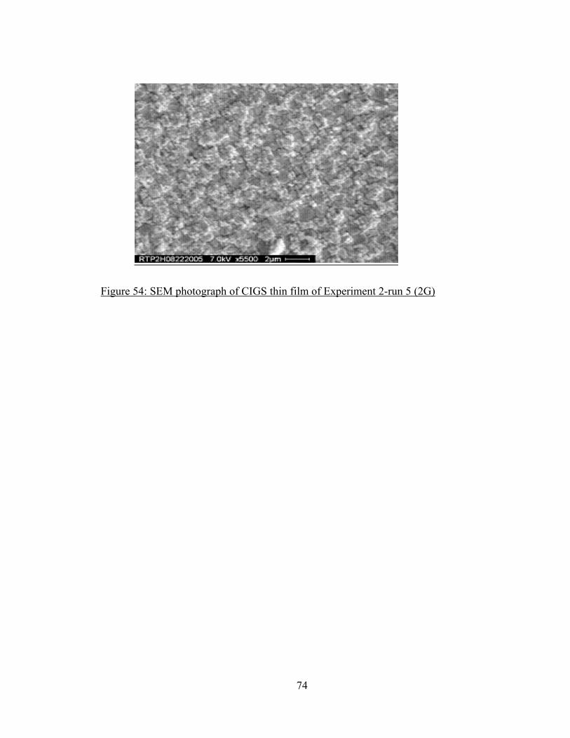
Figure 54: SEM photograph of CIGS thin film of Experiment 2-run 5 (2G)
74

Experiment 3
Deposition of CuGa and In was carried out with the following parameters:
Table 7: Deposition parameters for CuGa, In - Experiment 3
Time(sec/0.5”) Power (W) Voltage (V) Current (A) Pressure (mT)
CuGa 25.5 350 373
373
0.926
0.927
1.5
In 41.25 230 399
398
0.566
0.57
0.7
Figure 55: SEM photograph of unetched CIGS sample from Experiment 3
Thermal evaporation of NaF and Se was carried out similar to the previous
experiment. RTP was carried out within 310 seconds – temperature readings were not
75
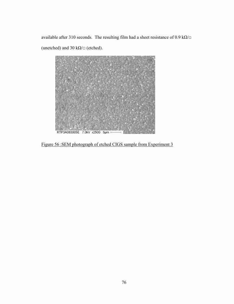
available after 310 seconds. The resulting film had a sheet resistance of 0.9 kΩ/
(unetched) and 30 kΩ/ (etched).
Figure 56 :SEM photograph of etched CIGS sample from Experiment 3
76
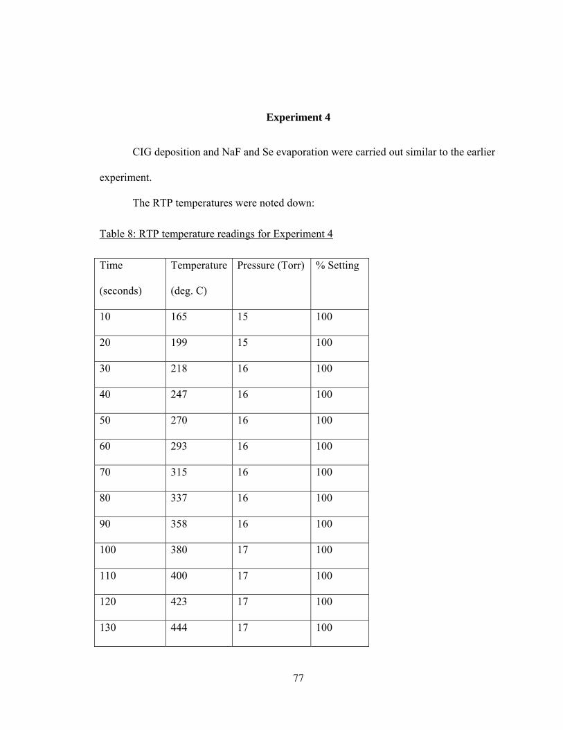
Experiment 4
CIG deposition and NaF and Se evaporation were carried out similar to the earlier
experiment.
The RTP temperatures were noted down:
Table 8: RTP temperature readings for Experiment 4
Time
(seconds)
Temperature
(deg. C)
Pressure (Torr) % Setting
10 165 15 100
20 199 15 100
30 218 16 100
40 247 16 100
50 270 16 100
60 293 16 100
70 315 16 100
80 337 16 100
90 358 16 100
100 380 17 100
110 400 17 100
120 423 17 100
130 444 17 100
77
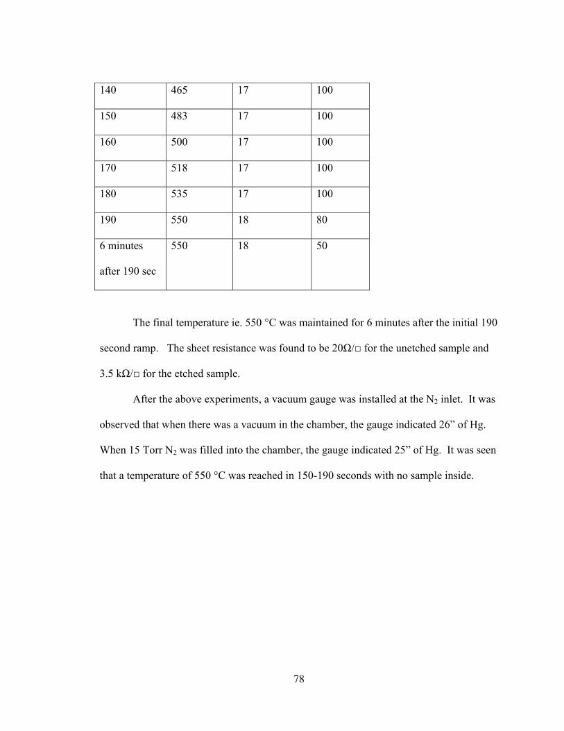
140 465 17 100
150 483 17 100
160 500 17 100
170 518 17 100
180 535 17 100
190 550 18 80
6 minutes
after 190 sec
550 18 50
The final temperature ie. 550 °C was maintained for 6 minutes after the initial 190
second ramp. The sheet resistance was found to be 20Ω/ for the unetched sample and
3.5 kΩ/ for the etched sample.
After the above experiments, a vacuum gauge was installed at the N2 inlet. It was
observed that when there was a vacuum in the chamber, the gauge indicated 26” of Hg.
When 15 Torr N2 was filled into the chamber, the gauge indicated 25” of Hg. It was seen
that a temperature of 550 °C was reached in 150-190 seconds with no sample inside.
78

Wt % At %
GaL 03.56 04.28
InL 33.98 24.80
CuK 18.04 23.79
SeK 44.42 47.14
Figure 57: XEDS data for Experiment 4
Figure 58: SEM photograph for etched sample of Experiment 4
79

Experiment 5
Deposition parameters for CuGa and In were as follows:
Table 9: Deposition parameters for CuGa, In – Experiment 5
Time(sec/0.5”) Power (W) Voltage (V) Current (A) Pressure (mT)
CuGa 25.5 350 375
373
0.922
0.926
1.5
In 41.25 230 403
403
0.563
0.561
0.7
NaF and Se are thermally evaporated - 3 mg NaF and 0.63 gm Se
Figure 59: Photograph of CIGS film after thermal evaporation
RTP was carried out with 15 Torr N2 similar to the previous experiment. The
unetched and etched samples showed a sheet resistance of 0.3 kΩ/ and 10 kΩ/
respectively. No Se deposits were observed on the top quartz plate. The solar cell was
80

completed by CdS deposition by CBD, ZnO deposition – 500 Å and Ni/Al fingers by e-
beam evaporation.
The completed solar cell yielded IV efficiencies of <1%. The I-V characteristics
were observed to be linear.
Experiment 6
It was thought that the intermixing of CuGa and In layers was not taking place
well during RTP. To promote intermixing, it was decided to deposit 9 alternating layers
of CuGa and In (4 In layers sandwiched between 5 CuGa layers) in stoichiometric
proportion.
Table 10: Deposition parameters for Experiment 6
Time(sec/0.5”) Power (W) Voltage (V) Current (A) Pressure (mT)
CuGa 5.1 350 372 0.93 1.5
In 10.31 230 420 0.539 0.7
CuGa 5.1 350 371 0.933 1.5
In 10.31 230 423 0.557 0.7
CuGa 5.1 350 371 0.932 1.5
In 10.31 230 424 0.536 0.7
CuGa 5.1 350 370 0.933 1.5
In 10.31 230 423 0.536 0.7
CuGa 5.1 350 370 0.933 1.5
81
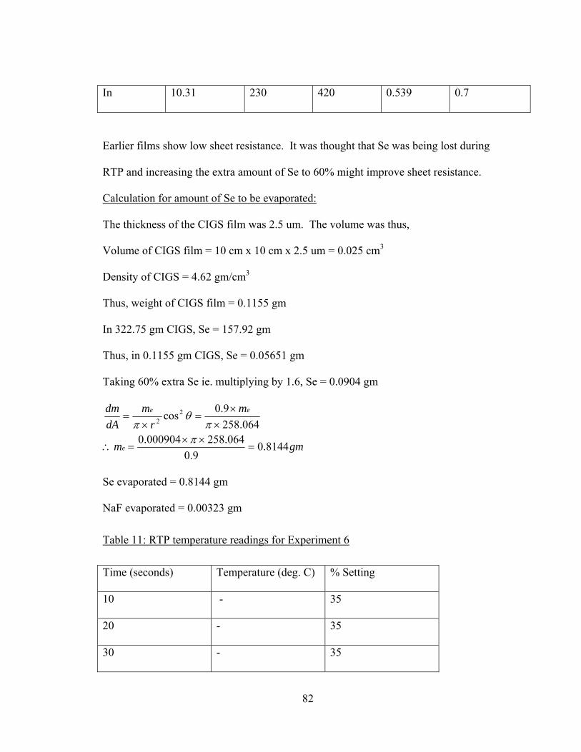
In 10.31 230 420 0.539 0.7
Earlier films show low sheet resistance. It was thought that Se was being lost during
RTP and increasing the extra amount of Se to 60% might improve sheet resistance.
Calculation for amount of Se to be evaporated:
The thickness of the CIGS film was 2.5 um. The volume was thus,
Volume of CIGS film = 10 cm x 10 cm x 2.5 um = 0.025 cm3
Density of CIGS = 4.62 gm/cm3
Thus, weight of CIGS film = 0.1155 gm
In 322.75 gm CIGS, Se = 157.92 gm
Thus, in 0.1155 gm CIGS, Se = 0.05651 gm
Taking 60% extra Se ie. multiplying by 1.6, Se = 0.0904 gm
gmm
mr
mdAdm
e
ee
8144.09.0
064.258000904.0064.258
9.0cos22
=××
=∴
××
=×
=
ππ
θπ
Se evaporated = 0.8144 gm
NaF evaporated = 0.00323 gm
Table 11: RTP temperature readings for Experiment 6
Time (seconds) Temperature (deg. C) % Setting
10 - 35
20 - 35
30 - 35
82

40 - 35
50 80 35
The same temperature was maintained for 15 minutes to promote
intermixing of precursors. The stopwatch was started again after 15
minutes.
10 168 100
20 215 100
30 247 100
40 277 100
50 304 100
60 330 100
70 354 100
80 375 100
90 397 100
Soak for 1 minute at 400 deg C. Power setting is 65-80 %
Soak for 5 minutes at 50-55 % power setting
Sheet resistance was found out to be 6 kΩ/ for the unetched sample and 400
kΩ/ for the etched sample.
In the second run, 30 Torr of H2 was mixed with 15 Torr of H2S were added to the
chamber. A second quartz plate was added to support the thermocouple. After reaching
80 °C, the sample was soaked at this temperature for 15 minutes. The power setting was
83
then increased to 100% and a temperature of 434 °C was reached within the next 130
seconds. After soaking the sample at this temperature for 1 minute, the power setting
was reduced to 50-55% and the sample was exposed to H2S atmosphere for 5 minutes.
Power was switched off after this. The unetched sample had a sheet resistance of 10
kΩ/, while the etched sample had a sheet resistance of 0.2 MΩ/.
After CdS was deposited, 500 Å ZnO (intrinsic) was deposited by RF sputtering
at 200W, 1.5 mT. (76V DC Bias, speed – 26 sec/0.5”). A 6000 Å thick layer of ZnO:Al
was deposited at 400W, 1.5 mT (121V DC Bias, speed – 150 sec/0.5”). The sheet
resistance was found to be 130 Ω/ (very high). Hence a 6000 Å layer of ZnO:Al was
again deposited at 425W, 1.5 mT. The sheet resistance was found to be 40 Ω/. Contact
fingers were deposited by evaporation of Cr/Ag. After I-V measurements, the best cell
had an efficiency of 2.42%. For the next sample, CdS and ZnO thickness will be
increased.
In the last experiment, a temperature of 120 °C was maintained for 30 minutes.
The sample was soaked for 2 minutes at 550 °C after which it was exposed to H2S
atmosphere for 5 minutes. The resulting cell had an efficiency of 3.86%.
84

CHAPTER SEVEN: CONCLUSIONS
The deposition mechanism for the DC magnetron sputtering chamber (for CuGa,
In and Mo) and RF magnetron sputtering chamber (for ZnO, ZnO:Al) was automated
with the help of a NI data acquisition card, stepper motor, stepper motor drive and a
power supply. Uniform CuGa, In and Mo precursor films are being prepared, valuable
time and energy is being saved. This mechanism could be scaled up in order to prepare
larger films. It is currently being upgraded to process multiple substrates in the same run.
Programming knowledge of LABVIEW was gained during the process of automation.
After fabrication of a solar cell, measurement of the I-V efficiency is of utmost
importance. Knowledge of various solar cell parameters such as fill factor (FF), open-
circuit voltage (Voc), short circuit current (Isc), efficiency (η), series resistance (Rs) and
parallel resistance(Rp) can be systematically used to a solar cell researcher’s advantage in
order to determine the methods to be used while fabricating future solar cells. A
LABVIEW program was custom-developed to instantly plot the I-V characteristics of a
solar cell and display these useful parameters. The measured values are saved into a file
for future reference.
Construction of a quantum efficiency setup was completed to analyze the spectral
response of completed solar cells. Comparison of measured QE values for a solar cell
with the reference curve already plotted at NREL was carried out. It was observed that
the measured values were within ±0.5% of the reference values.
Rapid Thermal Processing was initiated for CIGSS solar cell preparation.
Initially temperature v/s time graphs were plotted with various power settings to model
85

the RTP setup. It was possible to achieve a temperature of 500 °C in 120 minutes. In
the first experiment with a CIGS thin film substrate, it was observed that a N2 pressure of
at least 15 Torr was required to obtain a CIGS film that does not peel and has a sheet
resistance in the range >10 kΩ/. SEM shows formation of compact films with low
porosity, uniform grains of size > 1µm. XEDS results show near-stoichiometric
composition. The final experiment yielded a solar cell with efficiency – 3.86%, Voc –
0.59V, Isc - 7 mA, Fill factor – 41.24 %. These parameters were measured with the above
mentioned I-V measurement setup. Photovoltaic properties of solar cells shall be
improved by further optimization of deposition parameters and RTP process cycle times.
Regression analysis of PV modules was carried out with the regression program
that was built in-house to observe degradation trends in PV modules installed at the
FSEC test site. Data quality has improved considerably over the past few months since
the error-checking program is being used for troubleshooting daily data.
86

APPENDIX A: C SOURCE CODE FOR PROGRAM TO CHECK PV MODULE DATA
87
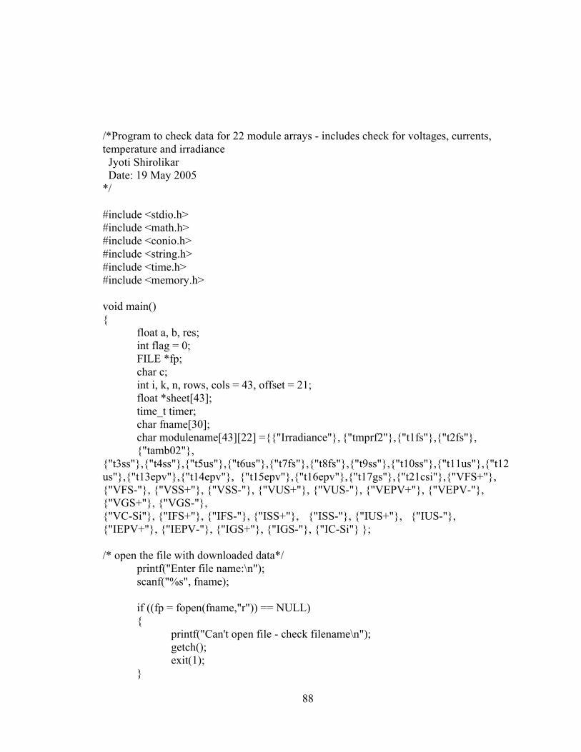
/*Program to check data for 22 module arrays - includes check for voltages, currents, temperature and irradiance Jyoti Shirolikar Date: 19 May 2005 */ #include <stdio.h> #include <math.h> #include <conio.h> #include <string.h> #include <time.h> #include <memory.h> void main() float a, b, res; int flag = 0; FILE *fp; char c; int i, k, n, rows, cols = 43, offset = 21; float *sheet[43]; time_t timer; char fname[30]; char modulename[43][22] ="Irradiance", "tmprf2","t1fs","t2fs", "tamb02", "t3ss","t4ss","t5us","t6us","t7fs","t8fs","t9ss","t10ss","t11us","t12us","t13epv","t14epv", "t15epv","t16epv","t17gs","t21csi","VFS+", "VFS-", "VSS+", "VSS-", "VUS+", "VUS-", "VEPV+", "VEPV-", "VGS+", "VGS-", "VC-Si", "IFS+", "IFS-", "ISS+", "ISS-", "IUS+", "IUS-", "IEPV+", "IEPV-", "IGS+", "IGS-", "IC-Si" ; /* open the file with downloaded data*/ printf("Enter file name:\n"); scanf("%s", fname); if ((fp = fopen(fname,"r")) == NULL) printf("Can't open file - check filename\n"); getch(); exit(1);
88

printf("\nEnter number of rows in .dat file (default = 96)-\n"); scanf("%d", &rows); n = rows; for (k=0; k<=(cols-1);k++) sheet[k] = (float*) malloc(n*sizeof(float)); /*scan excel sheet into arrays*/ for (i = 0;i<=(rows-1);i++) fscanf(fp, "%f\t%f\t%f\t%f\t%f\t%f\t%f\t%f\t%f\t%f\t%f\t%f\t%f\t%f\t%f\t%f\t%f\t%f\t%f\t%f\t%f\t%f\t%f\t%f\t%f\t%f\t%f\t%f\t%f\t%f\t%f\t%f\t%f\t%f\t%f\t%f\t%f\t%f\t%f\t%f\t%f\t%f\t%f", &(sheet[0][i]), &(sheet[1][i]), &(sheet[2][i]), &(sheet[3][i]), &(sheet[4][i]), &(sheet[5][i]),&(sheet[6][i]), &(sheet[7][i]),&(sheet[8][i]), &(sheet[9][i]),&(sheet[10][i]), &(sheet[11][i]),&(sheet[12][i]), &(sheet[13][i]),&(sheet[14][i]), &(sheet[15][i]), &(sheet[16][i]), &(sheet[17][i]), &(sheet[18][i]), &(sheet[19][i]), &(sheet[20][i]), &(sheet[21][i]), &(sheet[22][i]), &(sheet[23][i]), &(sheet[24][i]), &(sheet[25][i]), &(sheet[26][i]), &(sheet[27][i]), &(sheet[28][i]), &(sheet[29][i]), &(sheet[30][i]), &(sheet[31][i]), &(sheet[32][i]), &(sheet[33][i]), &(sheet[34][i]), &(sheet[35][i]), &(sheet[36][i]), &(sheet[37][i]), &(sheet[38][i]), &(sheet[39][i]), &(sheet[40][i]), &(sheet[41][i]), &(sheet[42][i]) ); /*close file*/ fclose(fp); fp = fopen("logfile.txt", "w"); timer = time(NULL); fprintf(fp, "Time: %s\n", asctime(localtime(&timer))); printf("Checking irradiance...\n"); for(i = 0;i<=(rows-1);i++) if((sheet[0][i]<-20) || (sheet[0][i]>1200)) fprintf(fp, "Error in irradiance at row no. %d \n", i+1); printf("Checking temperature ranges...\n"); for (i = 0;i<=(rows-1);i++) for (k = 1; k<=20;k++) if((sheet[k][i]<-1) || (sheet[k][i]>75))
89
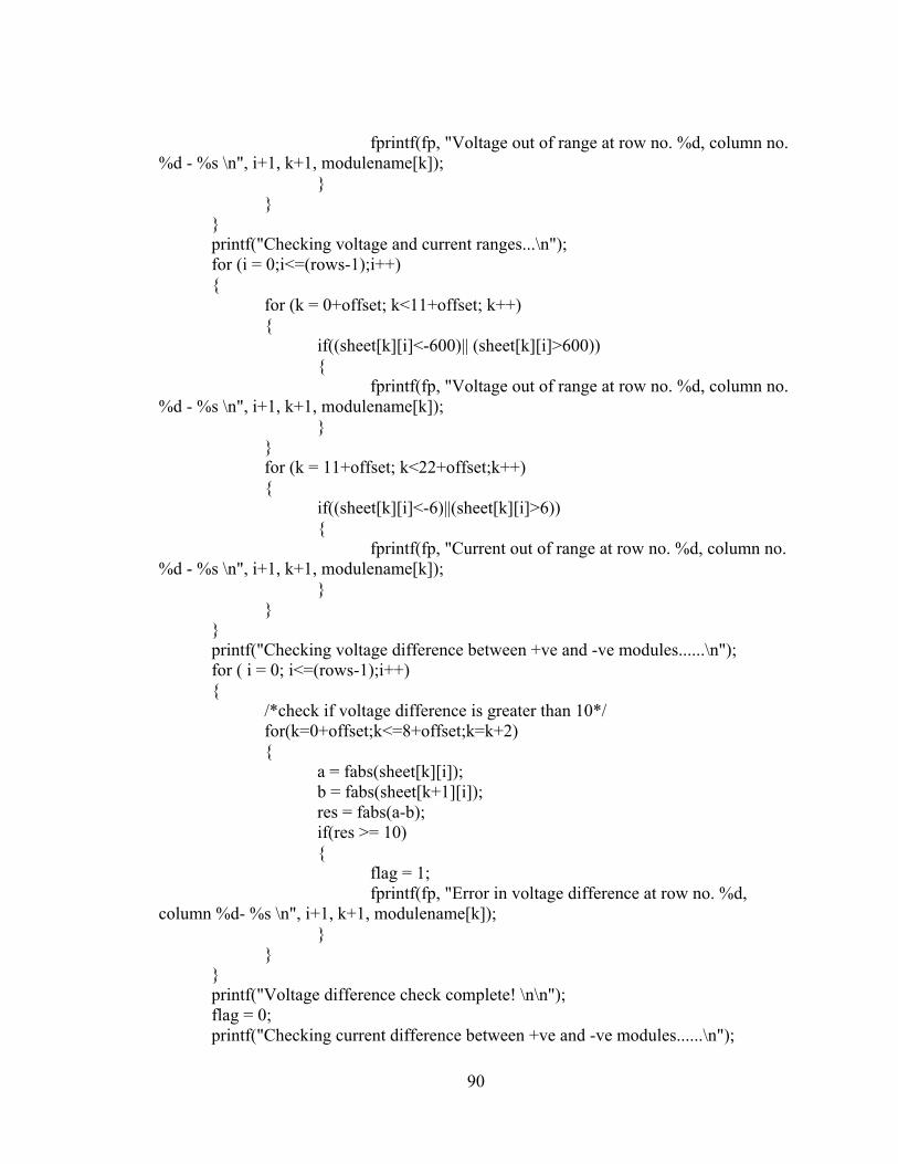
fprintf(fp, "Voltage out of range at row no. %d, column no. %d - %s \n", i+1, k+1, modulename[k]); printf("Checking voltage and current ranges...\n"); for (i = 0;i<=(rows-1);i++) for (k = 0+offset; k<11+offset; k++) if((sheet[k][i]<-600)|| (sheet[k][i]>600)) fprintf(fp, "Voltage out of range at row no. %d, column no. %d - %s \n", i+1, k+1, modulename[k]); for (k = 11+offset; k<22+offset;k++) if((sheet[k][i]<-6)||(sheet[k][i]>6)) fprintf(fp, "Current out of range at row no. %d, column no. %d - %s \n", i+1, k+1, modulename[k]); printf("Checking voltage difference between +ve and -ve modules......\n"); for ( i = 0; i<=(rows-1);i++) /*check if voltage difference is greater than 10*/ for(k=0+offset;k<=8+offset;k=k+2) a = fabs(sheet[k][i]); b = fabs(sheet[k+1][i]); res = fabs(a-b); if(res >= 10) flag = 1; fprintf(fp, "Error in voltage difference at row no. %d, column %d- %s \n", i+1, k+1, modulename[k]); printf("Voltage difference check complete! \n\n"); flag = 0; printf("Checking current difference between +ve and -ve modules......\n");
90

for ( i = 0; i<=(rows-1);i++) /*check if current difference is greater than 0.2*/ for(k=11+offset;k<=19+offset;k=k+2) a = fabs(sheet[k][i]); b = fabs(sheet[k+1][i]); res = fabs(a-b); if(res >= 0.2) flag = 1; fprintf(fp, "Error in current difference at row no. %d, column %d- %s \n", i+1, k+1, modulename[k]); printf("Current difference check complete! \n\n"); flag = 0; printf("Checking signs for positively biased modules.....\n"); for ( i = 0; i<=(rows-1);i++) /*check if positive modules have positive v, i within range*/ for (k= 0+offset; k<=10+offset; k=k+2) if(sheet[k][i]<0) flag = 1; fprintf(fp, "Negative value! Error at row no. %d, column %d- %s \n", i+1, k+1, modulename[k]); if(fabs(sheet[k][i])> 30000) fprintf(fp, "Out of range value at row no. %d, column %d- %s \n", i+1, k+1, modulename[k]); for (k= 11+offset; k<=21+offset; k=k+2) if(sheet[k][i]<0) flag = 1; fprintf(fp, "Negative value! Error at row no. %d, column %d- %s \n", i+1, k+1, modulename[k]); if(fabs(sheet[k][i])> 30000)
91

fprintf(fp, "Out of range value at row no. %d, column %d- %s \n", i+1, k+1, modulename[k]); printf("Sign check complete for positively biased modules!\n\n"); flag = 0; printf("Checking signs for negatively biased modules....\n"); for ( i = 0; i<=(rows-1);i++) /*check if negative modules have negative v, i within range*/ for (k= 1+offset; k<=9+offset; k=k+2) if(sheet[k][i]>0) flag = 1; fprintf(fp, "Positive value! Error at row no. %d, column %d- %s \n", i+1, k+1, modulename[k]); if(fabs(sheet[k][i])> 30000) fprintf(fp, "Out of range value at row no. %d, column %d- %s \n", i+1, k+1, modulename[k]); for (k= 12+offset; k<= 20+offset; k=k+2) if(sheet[k][i]>0) flag = 1; fprintf(fp, "Positive value! Error at row no. %d, column %d- %s \n", i+1, k+1, modulename[k]); if(fabs(sheet[k][i])> 30000) fprintf(fp, "Out of range value at row no. %d, column %d- %s \n", i+1, k+1, modulename[k]); printf("Sign check complete for negatively biased modules!\n\n"); flag = 0; printf("Exiting...\n"); fclose(fp);
92

/*free up memory*/ for (k=0; k<=(cols-1); k++) sheet[k] = NULL; free(sheet[k]);
93

APPENDIX B: PROCEDURE FOR CdS THIN FILM DEPOSITION ON CIGS FILMS
94

The general setup consists of a constant temperature, hot water bath, magnetic stirrer,
a reaction beaker (250 ml) and a mixing beaker (400 ml). Two CIGS samples are
suspended vertically with Teflon coated tweezers; a thermometer is also suspended in
the solution.
Stock solutions are made as follows:
• Cadmium sulfate 0.015 M; Thiourea, 1.5 M; and Ammonium Hydroxide, 28-
30% reagent, straight from the bottle. Thiourea solution is preferably filtered.
• Use CdSO4.8/3 H20 9 (Sigma, molecular weight is 256.46 g). To make a
0.015 M solution in 100 ml total volume, weight out 0.3847 g of the salt and
mix it in 100 ml of DI water.
• Use thiourea bottle (Fluka, molecular weight 76.116 g). To make a 1.5M
solution in 100 ml, weight out 11.417 g of thiourea and add it to 100 ml of
deionized water. To dissolve the thiourea, the solution needs to be stirred for
a while. Use a funnel and filter the solution into the flask.
Steps for CBD CdS
• Set the water bath to 65 °C. Have two CIGS samples mounted vertically and
appropriately with Teflon tweezers. Blow the samples with dry nitrogen prior
to mounting. The CIGS film surface faces the wall, and the sample must be
95

away from the center to avoid turbulence. Place a stir bar in the beaker but do
not stir yet. Suspend a thermometer in the solution.
• In a clean 500 ml beaker, mix 240 ml of deionized water, 37.5 ml of reagent
NH4OH 28-30%, 33 ml of 0.015M CdSO4 solution and 16.5 ml of the 1.5 M
thiourea solution (all at room temperature).
• Pour the (CdSO4 + NH4OH + thiourea) premixed solution in the reaction
beaker placed in the water bath held at 65°C and begin stirring. This is time t
= 0.
• The temperature of the solution will rise quickly (2 min, 48 °C, 3 min. 53°C, 4
min. 56-57 °C) since the beaker is already heated by water bath. Note the
temperature rise, the solution color and film color at 2, 3, 4, 6, 8, 10 min.
• In 10-11 min, the temperature will rise to 60°C. Typically a blue color,
indicative of CdS thickness of about 500 Å is observed. Purple to blue film
color is desirable.
• Remove the samples, dip in DI water, wash in running DI water and dry with
clean filtered nitrogen.
• Give a short anneal (1 min) at 200°C.
96

APPENDIX C: LIST OF ELECTRONIC COMPONENTS FOR AUTOMATION OF DEPOSITION MECHANISM
97

Name of the component Manufacturer Catalog/ Part # Price
Stepper motor - Holding
Torque = 180 oz-in
Current = 2.7A/phase
Pacific Scientific T21NRLH-LNN-
NS-00
$73.75
24V, 1.3A DC Power
Supply
Siemens 6EP1331-1SH02 $78.95
Stepper Drive (with cover,
heat sink and connector kit)
Pacific Scientific 6410-001-C-H-K
$366
New Low Price - NI PCI-
6024E Low-Cost
Multifunction I/O & NI-DAQ
National Instruments 777743-01 $517.50
SH68-68-EP Noise Rejecting,
Shielded Cable, 1 m
National Instruments 184749-01 $85.50
SCXI-1180 Feedthrough
Panel
National Instruments 776572-80 $85.50
SCXI-1302 Feedthrough
Terminal Block, Cast
National Instruments 777687-02 $157.50
Bracket/Adapter Assembly,
SCXI-1349
National Instruments 182671-01
$67.50
98

APPENDIX D: LIST OF ELECTRONIC COMPONENTS FOR CURRENT-VOLTAGE MEASUREMENT SETUP
99

Name of the component Manufacturer Catalog/Part# Price
20V, 5A Power Supply Kepco Power
Supplies
BOP 20-5D $1887.65
Remote Communication card Kepco Power
Supplies
BIT 4886 $688.75
6.5 digit multimeter Agilent
Technologies
34401A $895.26
Light source GE ELH 300W, 120V $14.99
GPIB card NI NI PCI IEEE 488.2
Micromanipulator probes Signatone S-600
100

APPENDIX E: TEMPERATURE PROFILES FOR RTP SETUP
101

Temperature vs Time
0
100
200
300
400
500
600
12 32 57 89 120
Time (seconds)
Tem
pera
ture
(deg
. C)
Figure 60: Temperature versus time graph for 100% power setting
Temperature vs Time
0
100
200
300
400
500
600
029
1930
4730
6031
8732
6336
1041
1245
98
Time(seconds)
Tem
pera
ture
(deg
C)
off
30%
40%
Figure 61: Temperature versus time graph for 30% for 48 minutes, 40% for 3 minutes
102

Temperature vs time
0
100
200
300
400
500
600
Time
Tem
pera
ture
Figure 62: Temperature versus time graph for 35% power setting
103

LIST OF REFERENCES
1. Stephen J. Fonash, ‘Solar cell device physics’, Academic Press, New York, pg 1., (1981)
2. H. P. Garg, J. Prakash, ‘Solar energy fundamentals and applications’, First revised
edition, Tata McGraw Hill Publishing Company,Ltd., India, pg 370 (2003).
3. Kuttath, S., ‘Process Optimization and characterization of CuInSe2 and CuIn1-xGaxSe2 polycrystalline thin film solar cells’, M.S. thesis, University of Central Florida, (1994)
4. K. L. Chopra and S. R. Das, ‘Why thin film solar cells’, Thin Film Solar Cell,
Plenum press – New York, pg 1-13 (1983)
5. Y. Hamakawa, ‘Thin Film Solar Cells – Next Generation Photovoltaics and Its Application’, Springer-Verlag, Berlin Heidelberg New York.
6. Wagner, S., Shay, J. L., Migliorato, P. and Kasper, H. M., ‘CuInSe2/CdS
heterojunction photovoltaic detectors’, Appl. Phys. Lett. 25, 434-435 (1974).
7. Kazmerski, L. L., Ayyagari, M. S., Juang, Y. J., R.P. Patterson, R.P., ‘Growth and Characterization of Thin Film Compound Semiconductor Heterojunctions’, J. Vac. Sci. Technol. 13, pg 65 (1977).
8. U. Rau, M. Schmidt, A. Jasenek, G. Hanna and H.W. Schock, Solar Energy
Materials & Solar Cells 67, pg 137-143 (2001).
9. Pethe, S. ‘Optimization of the two stage process for Cu(In, Ga)Se2 solar cells’, M. S. Thesis, University of South Florida, (2004).
10. Tom Markvart and Luis Castaner, ‘Solar Cells Materials, Manufacture and
Operation’, Elsevier Advanced Technology, UK (2005)
11. R. Singh, K.C. Cherukuri, L. Vedula, A. Rohatgi, and S. Narayanan, ‘Low Temperature Shallow Junction Formation Using Vacuum Ultraviolet Photons in Rapid Isothermal Processing’, Appl. Phys. Lett., Vol. 70, No. 13, pp. 1700-1702, (1997)
12. V. Probst, W. Stetter, W. Riedl, H. Vogt, M. Wendl, H. Calwer, S. Zweigart, K.-
D. Ufert, B. Freienstein, H. Cerva, F.H. Karg, ‘Rapid CIS-process for high efficiency PV-modules: development towards large area processing’, Thin Solid Films, Vol. 387, pp. 262-267, (2001)
104

13. Ankur Kadam, ‘Development of large area CIGS2 thin film solar cells on stainless steel foil for space applications’, MS Thesis, University of Central Florida, (2002)
14. C. R. Osterwald et. al, ‘Resistive Loading of Photovoltaic Modules and Arrays for
Long-Term Exposure Testing’, National Renewable Energy Laboratory
105


