Q105 Repair Guide
V1.0
Prepared by shujun.bao Date 2012-10-09
Reviewed by Xu.wu Date 2012-10-09
All rights reserved

Q105 Repair Guide V1.2
2012-10-09
Revision record
Date
Revision
Version
Revision Cause
Section Number
Change
Description
Author
2012-10-09 V1.0 Q105 MP Shujun.bao
Q105 Repair Guide
2012-10-09
Contents
Contents ................................................................................................................................. 3
1. Introduction ......................................................................................................................... 4
1.1 Objective ....................................................................................................................... 4
1.2 General Safety notice .................................................................................................... 4
1.3 Use Instruction .............................................................................................................. 4
2. Technology summarize ...................................................................................................... 5
2.1 Description of main board component map ................................................................... 5
2.2 MSM7225A circuit system ............................................................................................. 7
2.3 Base band circuit ........................................................................................................... 8
2.4 Power Management circuit ............................................................................................ 9
2.5 BT/FM circuit ............................................................................................................... 11
2.6 RF circuit ..................................................................................................................... 11
3. Trouble Shooting .............................................................................................................. 12
3.1 Fail to startup/power on ............................................................................................... 12
3.2 Fail to charge ............................................................................................................... 13
3.3 Fail to display .............................................................................................................. 14
3.4 Fail to call .................................................................................................................... 15
3.5 Speaker no sound ....................................................................................................... 16
3.6 Earphone fail ............................................................................................................... 17
3.7 Vibrator fail .................................................................................................................. 19
3.8 Side key fail ................................................................................................................. 19
3.9 Failure to identify SIM card .......................................................................................... 20
3.10 Failure to identify SIM card ........................................................................................ 20
3.11 Camera fail ................................................................................................................ 21
3.12 Failure to read T-flash card ....................................................................................... 22
4. BGA related GND or no function pad ............................................................................... 23
4.1 CPU and memory pin map .......................................................................................... 23
4.2 PMU pin map ............................................................................................................... 24
4.3 BT/FM/WIFI pin map ................................................................................................... 25
Q105 Repair Guide
2012-10-09
1. Introduction
1.1 Objective
The manual is not a general publication but only edited for experienced technician. The main purpose is to provide basic foundation for the electrical & mechanical maintenance.
1.2 General Safety notice
1) Only experienced technician can repair with this guide during product is power on. Any maintenance by other non-technicians will cause serious damage of the handset. Neither short circuit nor counter-polarity connection is allowed for any electronic part in the handset.
3) Be careful of ESD protection during maintenance to avoid the damage of electrostatic sensitive components on the handset.
4) If disassembling operation is necessary for repairing, comply with mechanical structure disassembling work instruction. Otherwise, disassembling operation will make the handset damaged.
1.3 Use Instruction
1) Avoid using handset in conditions following: Where there is any caustic liquid or gas Where there is any high-temperature or fire circumstance Where there is any flammable liquid or gas
2) Do not use handset while driving for your safety; 3) Please comply with corresponding rules in some special occasions (like in operating
room, in airplane) 4) Accessory purchasing or changing should comply with model matching; 5) If need clean handset surface, please use cloth dipping a little clean water. Do not use
soluble cleanser.
Q105 Repair Guide
2012-10-09
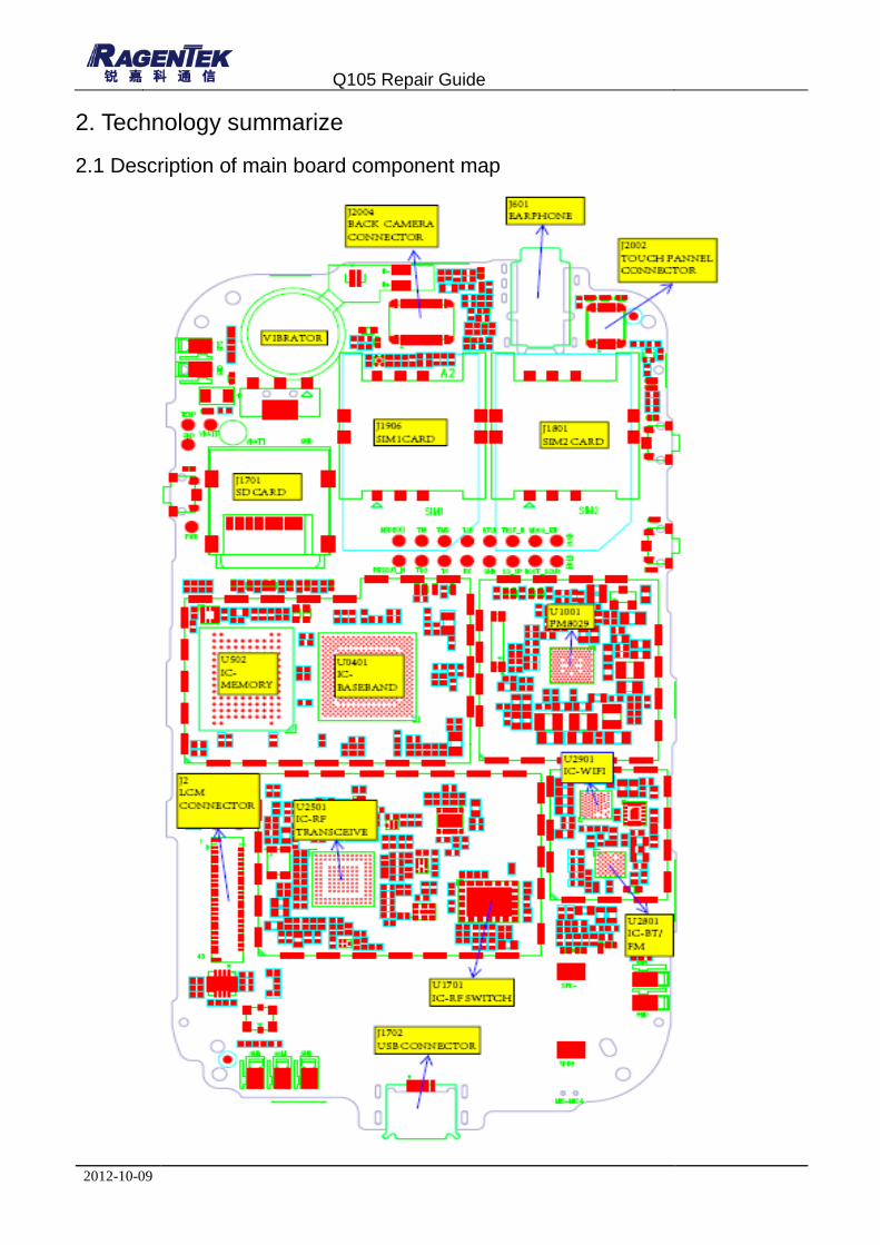
2. Technology summarize
2.1 Description of main board component map

Q105 Repair Guide
2012-10-09

Q105 Repair Guide
2012-10-09
2.2 MSM7225A circuit system
MSM7225A functional block diagram as following:
MSM7225A functional system is made of three parts as below: Digital baseband function: Memory, LCM, GPIO interface, Keypad interface etc.
Analog baseband function: AUDIO(including MIC, Receiver, Speaker),Camera, Video,
Ambient light and Proximity sensor, Power management, RTC, Charge control, etc. RF function: RF front-end module, Antenna, RF transceiver, GSM/WCDMA communication system, etc.

Q105 Repair Guide
2012-10-09
2.3 Base band circuit
MSM7225A baseband System Architecture as following:
Processing features:
◆ High-performance ARM CORTEX A5 800 MHz application processor :
1) ARM architecture v7
2) 32 KB instruction and 32 KB data cache
3) 256 KB ARM L2 cache (L2C - 310)
4) 8-stage In-order pipeline with dynamic branch prediction
5) Supports the ARM and Thumb instruction sets, and Jazelle technology to enable direct execution of Java byte-codes
◆ Industry standard ARM926EJ-S 400 MHz embedded microprocessor subsystem 1) 16 KB instruction and 16 KB data cache 2) ARM version 5TEJ instructions 3) Higher performance five-stage pipeline, Harvard cached architecture 4) Higher internal CPU clock rate with on-chip cache 5) Internal watchdog and sleep timers
◆ QDSP5000 350 MHz application digital signal processing (ADSP) 1) 512 KB L2 cache

Q105 Repair Guide
2012-10-09
◆ QDSP4000 122.88 MHz modem digital signal processing (MDSP)
Memory support features
◆ 256 KB internal memory (IMEM) for graphics, internal functions, DSP, etc.
◆ Dual-memory buses separating the high-speed memory subsystem (EBI1) from low-speed peripherals (EBI2) such as LCD panels
◆ Enhanced EBI1 memory support: 200 MHz bus clock for DDR SDRAM
◆ EBI2 support: 1) 1.8V memory interface support 2) Support for EBI2 A-D muxed mode 3) NAND flash memory interface 4) Support for 8-bit BCH ECC 5) Boot from NAND (One NAND not supported) 6) LCD
2.4 Power Management circuit
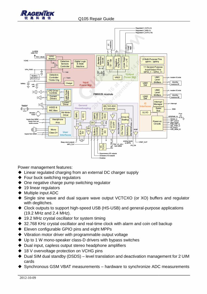
The PM8029 device integrates all wireless handset power-management, general house -keeping, and user-interface support functions into a single mixed-signal IC. This mixed-signal BiCMOS device is available in the 140-pin Wafer Level Nano-Scale Package (140 WLNSP), which includes several ground pins for electrical ground and thermal relief. Power management functional block diagram as following:
Q105 Repair Guide
2012-10-09
Power management features:
◆ Linear regulated charging from an external DC charger supply
◆ Four buck switching regulators
◆ One negative charge pump switching regulator
◆ 19 linear regulators
◆ Multiple input ADC
◆ Single sine wave and dual square wave output VCTCXO (or XO) buffers and regulator with deglitches.
◆ Clock outputs to support high-speed USB (HS-USB) and general-purpose applications
(19.2 MHz and 2.4 MHz).
◆ 19.2 MHz crystal oscillator for system timing
◆ 32.768 KHz crystal oscillator and real-time clock with alarm and coin cell backup
◆ Eleven configurable GPIO pins and eight MPPs
◆ Vibration motor driver with programmable output voltage
◆ Up to 1 W mono-speaker class-D drivers with bypass switches
◆ Dual input, capless output stereo headphone amplifiers
◆ 18 V overvoltage protection on VCHG pins
◆ Dual SIM dual standby (DSDS) – level translation and deactivation management for 2 UIM
cards
◆ Synchronous GSM VBAT measurements – hardware to synchronize ADC measurements
Q105 Repair Guide
2012-10-09
with GSM transmit pulse
◆ PDM flip-flop – built-in voltage leveling and clock synchronization flip-flop
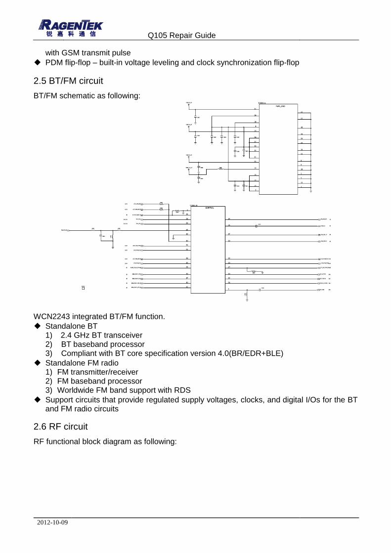
2.5 BT/FM circuit
BT/FM schematic as following:
WCN2243 integrated BT/FM function.
◆ Standalone BT 1) 2.4 GHz BT transceiver 2) BT baseband processor 3) Compliant with BT core specification version 4.0(BR/EDR+BLE)
◆ Standalone FM radio 1) FM transmitter/receiver 2) FM baseband processor 3) Worldwide FM band support with RDS
◆ Support circuits that provide regulated supply voltages, clocks, and digital I/Os for the BT and FM radio circuits
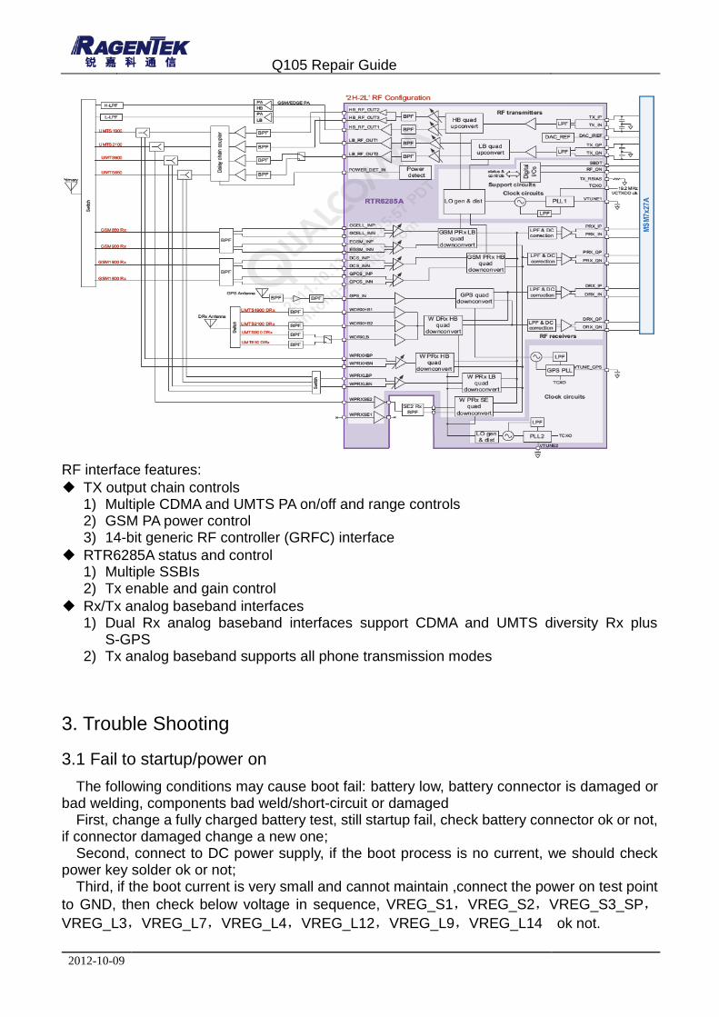
2.6 RF circuit
RF functional block diagram as following:
Q105 Repair Guide
2012-10-09
RF interface features:
◆ TX output chain controls 1) Multiple CDMA and UMTS PA on/off and range controls 2) GSM PA power control 3) 14-bit generic RF controller (GRFC) interface
◆ RTR6285A status and control 1) Multiple SSBIs 2) Tx enable and gain control
◆ Rx/Tx analog baseband interfaces 1) Dual Rx analog baseband interfaces support CDMA and UMTS diversity Rx plus
S-GPS 2) Tx analog baseband supports all phone transmission modes
3. Trouble Shooting
3.1 Fail to startup/power on
The following conditions may cause boot fail: battery low, battery connector is damaged or bad welding, components bad weld/short-circuit or damaged
First, change a fully charged battery test, still startup fail, check battery connector ok or not, if connector damaged change a new one;
Second, connect to DC power supply, if the boot process is no current, we should check power key solder ok or not;
Third, if the boot current is very small and cannot maintain ,connect the power on test point
to GND, then check below voltage in sequence, VREG_S1,VREG_S2,VREG_S3_SP,
VREG_L3,VREG_L7,VREG_L4,VREG_L12,VREG_L9,VREG_L14 ok not.

Q105 Repair Guide
2012-10-09
Fourth, if the current stay in 40mA, we should check the circuit around flash, when CPU calling program from flash fail, the current will stay in 40mA, re-download the software or change a new flash or CPU.
3.2 Fail to charge
Check charging circuit related component, check below information in sequence: First, checks whether boot normal use the battery, if not check battery connector solder ok
or not; Second, check USB connector on board solder ok or not; Third, check T1710 whether reverse, check C1802 resistance is very big or not. Fourth, check U1001 solder ok or not, re-hot U1001 or change a new one.
Fail to power on
Check if the battery is OK.
Change battery
Check if battery connects solder ok
Is power key OK?
Check each power out of PMU
Resold connect
Change a new power key
Re-solder or replace U1001
Re-download Software
OK
Y
N
N
N
N
Y
Y
Y
Y
OK
N
Y
N
Resold or replace U502
Resold or replace U0401
OK Y
Q105 Repair Guide
2012-10-09
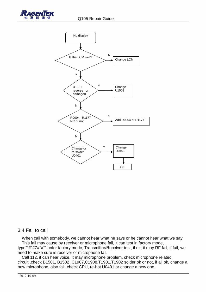
3.3 Fail to display
The screen dose not shines or shows white: First, use DC power supply to start-up, check the board whether power on normal, ensure main board can power on normal Second, check LCD module, change a new module, check whether can display normal, Third, check R0004, R1177, U1501 solder ok or not Fourth, use oscilloscope to test LCD_BACKLIGHT_EN, check it whether high, if not, check R1507 resistance, U0401 solder ok or not, re-hot U0401or check a new one.
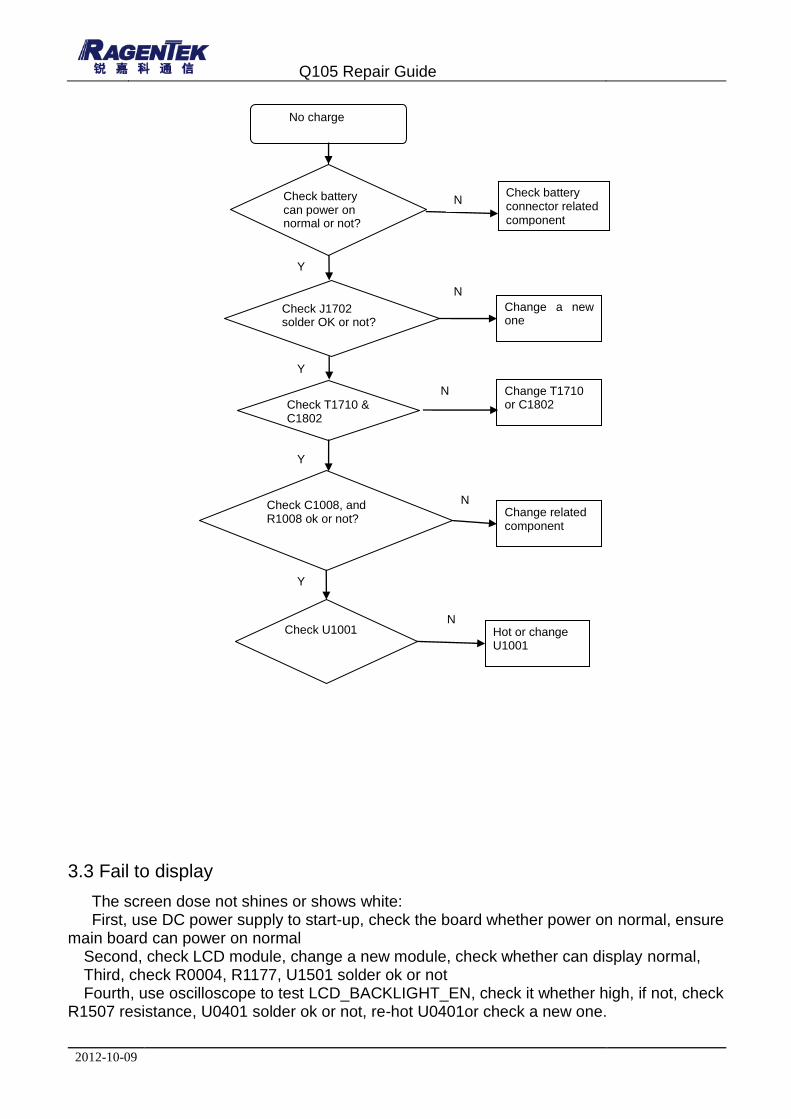
No charge
Check battery can power on normal or not?
Check battery connector related component
Check J1702 solder OK or not?
Check T1710 & C1802
Check C1008, and R1008 ok or not?
Change a new one
Change T1710 or C1802
Change related component
Check U1001 Hot or change U1001
Y
N
N
N
N
N
Y
Y
Y
Q105 Repair Guide
2012-10-09
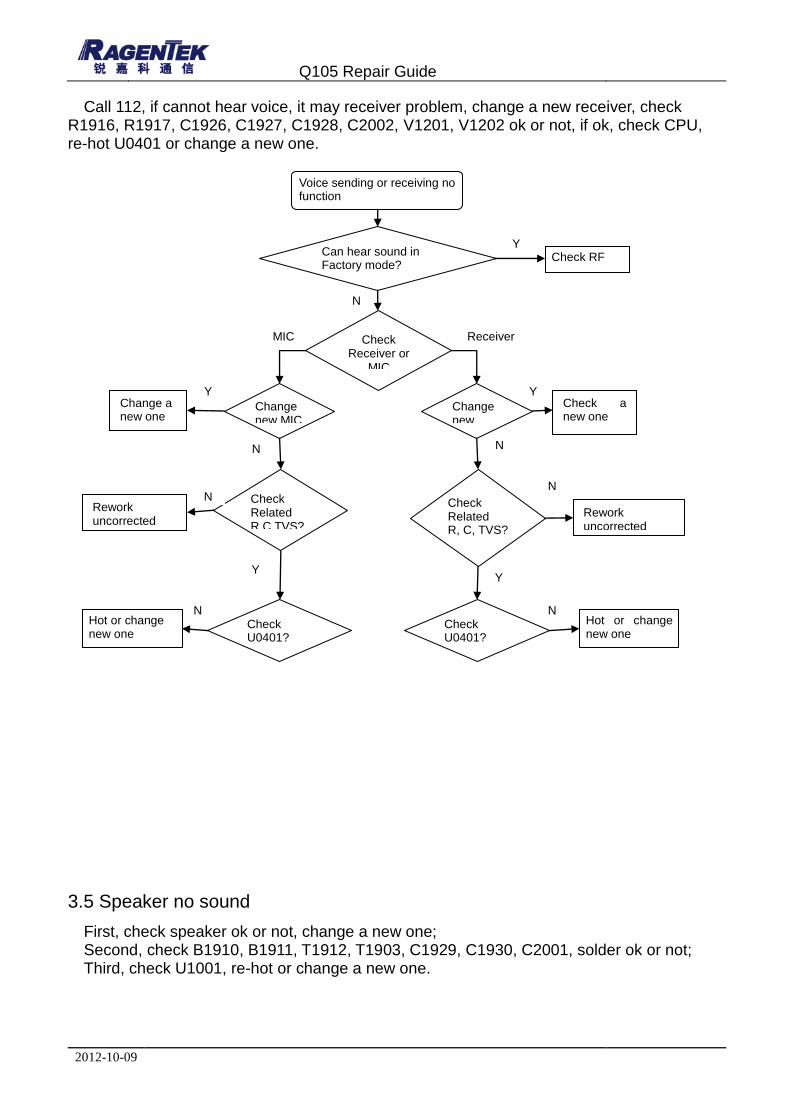
3.4 Fail to call
When call with somebody, we cannot hear what he says or he cannot hear what we say: This fail may cause by receiver or microphone fail, it can test in factory mode, type“*#*#7#*#*” enter factory mode, Transmitter/Receiver test, if ok, it may RF fail, if fail, we need to make sure is receiver or microphone fail.
Call 112, if can hear voice, it may microphone problem, check microphone related circuit ,check B1501, B1502 ,C1907,C1908,T1901,T1902 solder ok or not, if all ok, change a new microphone, also fail, check CPU, re-hot U0401 or change a new one.
No display
Is the LCM well? Change LCM
U1501 reverse or damaged
R0004, R1177 NC or not
Change U1501
Add R0004 or R1177
Change or re-solder U0401
Change U0401
OK
N
Y
N
Y
N
Y
Y
Q105 Repair Guide
2012-10-09
Call 112, if cannot hear voice, it may receiver problem, change a new receiver, check R1916, R1917, C1926, C1927, C1928, C2002, V1201, V1202 ok or not, if ok, check CPU, re-hot U0401 or change a new one.
3.5 Speaker no sound
First, check speaker ok or not, change a new one; Second, check B1910, B1911, T1912, T1903, C1929, C1930, C2001, solder ok or not; Third, check U1001, re-hot or change a new one.
Voice sending or receiving no function
Can hear sound in Factory mode?
Check RF
Check Receiver or
MIC
problem?
Hot or change new one
Y
N
Receiver
Y
N
Y
Check Related R, C, TVS?
Check U0401?
Change new REC
Check a new one
Rework uncorrected component
N
N Hot or change new one
Check Related R C TVS?
Check U0401?
Change new MIC
Change a new one
Rework uncorrected component
MIC
Y
N
N
Y
N
Y

Q105 Repair Guide
2012-10-09
3.6 Earphone fail
No sound
Is speaker OK? Replace Speaker
Are B1910, B1911
NC or not?
Check T1912, T1903, C1929, C1930, and C2001 ok or not?
Check U1001
ADD B1910,B1911
Re-solder uncorrected component
Hot or change U1001
Y
N
Y
N
N
Y
N

Q105 Repair Guide
2012-10-09
No sound in earphone
Is earphone connector OK?
Replace earphone
Is J601 soldering well?
Are All TVS right direction?
Related R, C right?
Re-solder J601
Re-solder uncorrected TVS
Re-solder uncorrected R C
Y
N
N
N
Y
Y
N
Hot or change U1001
OK
Y

Q105 Repair Guide
2012-10-09
3.7 Vibrator fail
3.8 Side key fail
Side key no function
Is key switch soldering OK?
Re-solder or change new one
Is R1469, R1435, R1497, and R1921 NC or not?
Check U0401
Solder 1K resistance
Re-sold or change U0401
Y
N
Y
N
Y
Motor doesn’t work
Supply 3.3V for motor, test motor can work or not
Change a new Motor
Check related R, C OK or NOT, Check D1201 reverses or not
Hot U1001 or Change a new one
Change uncorrected component
OK
Y
N
N
Y
Q105 Repair Guide
2012-10-09
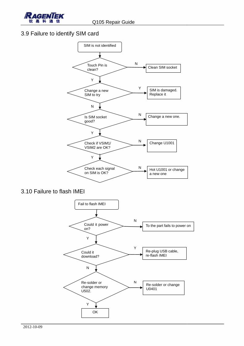
3.9 Failure to identify SIM card
3.10 Failure to flash IMEI
Fail to flash IMEI
Could it power on?
To the part fails to power on
Could it download?
Re-solder or change memory U502.
Re-plug USB cable, re-flash IMEI
Re-solder or change U0401
OK
N
Y
N
N
Y
Y
SIM is not identified
Touch Pin is clean?
Clean SIM socket
Change a new SIM to try
Is SIM socket good?
SIM is damaged. Replace it
Change a new one.
Check if VSIM1/ VSIM2 are OK?
Change U1001
N
Y
N
N
Y
Y
Y
Check each signal on SIM is OK?
Hot U1001 or change a new one
N
N

Q105 Repair Guide
2012-10-09
3.11 Camera fail
First, change a new camera module, check camera connector ok or not; Second, check AVDD, DOVDD. Third, use oscilloscope to test I2C, CAM_RST, CAM_MCLK, CAM_PCLK, MIPI_DATA,
and MIPI_CLK. If signals abnormal check U0401, re-hot or change a new one.
Camera fail
Is camera connector soldering well?
Re-solder or change new one
Check camera ok or not?
Check AVDD DOVDD ok or not?
Check each signal of Camera is ok or not?
Change a new camera
Hot U1001 or change a new one
Hot U0401 or change a new one
Y
N
N
N
Y
Y
N

Q105 Repair Guide
2012-10-09
3.12 Failure to read T-flash card
First, change another T flash card, check whether T flash card bad or not Second, check card connector solder ok or not, if fail, re-solder or change a new one Third, check TVS reserved or not, check VDD whether normal Fourth, test related signals, such as MCCK, MCCM0, MCDA0, MCDA1…MCDA3, if abnormal, check U0401, re-hot or change a new one.
T-F Card is not identified
Change a new TF-card to test
T-F card is damaged. Replace it
Check T flash card socket ok or not?
Check TVS reverse or not?
Re-solder it or change new one
Solder it correct
Check VDD OK or not?
Hot U1001 or change new one
Y
N
N
N
Y
Y
N
Check each signal OK or not?
Hot U0401 or change new one
N
N

Q105 Repair Guide
2012-10-09
4. BGA related GND or no function pad
Red--------no function pad White------GND pad
4.1 CPU and memory pin map

Q105 Repair Guide
2012-10-09
4.2 PMU pin map

Q105 Repair Guide
2012-10-09
4.3 BT/FM/WIFI pin map


