

RADIO-FREQUENCYAND MICROWAVECOMMUNICATIONCIRCUITS

RADIO-FREQUENCYAND MICROWAVECOMMUNICATIONCIRCUITS
Analysis and Design
Second Edition
Devendra K. MisraUniversity of Wisconsin–Milwaukee
A JOHN WILEY & SONS, INC., PUBLICATION

Copyright 2004 by John Wiley & Sons, Inc. All rights reserved.
Published by John Wiley & Sons, Inc., Hoboken, New Jersey.Published simultaneously in Canada.
No part of this publication may be reproduced, stored in a retrieval system, or transmitted inany form or by any means, electronic, mechanical, photocopying, recording, scanning, orotherwise, except as permitted under Section 107 or 108 of the 1976 United States CopyrightAct, without either the prior written permission of the Publisher, or authorization throughpayment of the appropriate per-copy fee to the Copyright Clearance Center, Inc., 222Rosewood Drive, Danvers, MA 01923, 978-750-8400, fax 978-646-8600, or on the web atwww.copyright.com. Requests to the Publisher for permission should be addressed to thePermissions Department, John Wiley & Sons, Inc., 111 River Street, Hoboken, NJ 07030,(201) 748-6011, fax (201) 748-6008.
Limit of Liability/Disclaimer of Warranty: While the publisher and author have used theirbest efforts in preparing this book, they make no representations or warranties with respect tothe accuracy or completeness of the contents of this book and specifically disclaim anyimplied warranties of merchantability or fitness for a particular purpose. No warranty may becreated or extended by sales representatives or written sales materials. The advice andstrategies contained herein may not be suitable for your situation. You should consult with aprofessional where appropriate. Neither the publisher nor author shall be liable for any lossof profit or any other commercial damages, including but not limited to special, incidental,consequential, or other damages.
For general information on our other products and services please contact our Customer CareDepartment within the U.S. at 877-762-2974, outside the U.S. at 317-572-3993 orfax 317-572-4002.
Wiley also publishes its books in a variety of electronic formats. Some content that appearsin print, however, may not be available in electronic format.
Library of Congress Cataloging-in-Publication Data:
Misra, Devendra, 1949–Radio-frequency and microwave communication circuits : analysis and
design / Devendra K. Misra.—2nd ed.p. cm.
Includes bibliographical references and index.ISBN 0-471-47873-3 (Cloth)
1. Radar circuits–Design and construction. 2. Microwavecircuits–Design and construction. 3. Electronic circuit design. 4.Radio frequency. I. Title.TK6560 .M54 2004621.384′12–dc22
2003026691
Printed in the United States of America.
10 9 8 7 6 5 4 3 2 1
CONTENTS
Preface ix
1 Introduction 1
1.1 Microwave Transmission Lines 41.2 Transmitter and Receiver Architectures 8
2 Communication Systems 11
2.1 Terrestrial Communication 122.2 Satellite Communication 132.3 Radio-Frequency Wireless Services 162.4 Antenna Systems 182.5 Noise and Distortion 33
Suggested Reading 52Problems 52
3 Transmission Lines 57
3.1 Distributed Circuit Analysis of Transmission Lines 573.2 Sending-End Impedance 673.3 Standing Wave and Standing Wave Ratio 803.4 Smith Chart 85
Suggested Reading 95Problems 95
v
vi CONTENTS
4 Electromagnetic Fields and Waves 104
4.1 Fundamental Laws of Electromagnetic Fields 1044.2 The Wave Equation and Uniform Plane Wave Solutions 1144.3 Boundary Conditions 1194.4 Uniform Plane Wave Incident Normally on an Interface 1234.5 Modified Maxwell’s Equations and Potential Functions 1264.6 Construction of Solutions 1304.7 Metallic Parallel-Plate Waveguide 1334.8 Metallic Rectangular Waveguide 1374.9 Metallic Circular Waveguide 142
Suggested Reading 145Problems 145
5 Resonant Circuits 151
5.1 Series Resonant Circuits 1515.2 Parallel Resonant Circuits 1605.3 Transformer-Coupled Circuits 1645.4 Transmission Line Resonant Circuits 1705.5 Microwave Resonators 177
Suggested Reading 184Problems 184
6 Impedance-Matching Networks 189
6.1 Single Reactive Element or Stub Matching Networks 1906.2 Double-Stub Matching Networks 2026.3 Matching Networks Using Lumped Elements 207
Suggested Reading 226Problems 226
7 Impedance Transformers 234
7.1 Single-Section Quarter-Wave Transformers 2347.2 Multisection Quarter-Wave Transformers 2377.3 Transformer with Uniformly Distributed Section Reflection
Coefficients 2397.4 Binomial Transformers 2447.5 Chebyshev Transformers 2487.6 Exact Formulation and Design of Multisection Impedance
Transformers 2557.7 Tapered Transmission Lines 2637.8 Synthesis of Transmission Line Tapers 2707.9 Bode–Fano Constraints for Lossless Matching Networks 280

CONTENTS vii
Suggested Reading 281Problems 281
8 Two-Port Networks 283
8.1 Impedance Parameters 2848.2 Admittance Parameters 2898.3 Hybrid Parameters 2968.4 Transmission Parameters 2988.5 Conversion of Impedance, Admittance, Chain, and Hybrid
Parameters 3048.6 Scattering Parameters 3048.7 Conversion From Impedance, Admittance, Chain, and Hybrid
Parameters to Scattering Parameters, or Vice Versa 3238.8 Chain Scattering Parameters 325
Suggested Reading 325Problems 326
9 Filter Design 333
9.1 Image Parameter Method 3349.2 Insertion-Loss Method 3539.3 Microwave Filters 380
Suggested Reading 389Problems 389
10 Signal-Flow Graphs and Their Applications 392
10.1 Definitions and Manipulation of Signal-Flow Graphs 39610.2 Signal-Flow Graph Representation of a Voltage Source 40110.3 Signal-Flow Graph Representation of a Passive Single-Port
Device 40210.4 Power Gain Equations 410
Suggested Reading 417Problems 418
11 Transistor Amplifier Design 422
11.1 Stability Considerations 42211.2 Amplifier Design for Maximum Gain 42911.3 Constant-Gain Circles 43911.4 Constant Noise Figure Circles 45711.5 Broadband Amplifiers 46611.6 Small-Signal Equivalent-Circuit Models of Transistors 46911.7 DC Bias Circuits for Transistors 472

viii CONTENTS
Suggested Reading 475Problems 476
12 Oscillator Design 479
12.1 Feedback and Basic Concepts 47912.2 Crystal Oscillators 49212.3 Electronic Tuning of Oscillators 49412.4 Phase-Locked Loop 49712.5 Frequency Synthesizers 51612.6 One-Port Negative Resistance Oscillators 52012.7 Microwave Transistor Oscillators 523
Suggested Reading 538Problems 538
13 Detectors and Mixers 543
13.1 Amplitude Modulation 54413.2 Frequency Modulation 55513.3 Switching-Type Mixers 55913.4 Conversion Loss 56513.5 Intermodulation Distortion in Diode-Ring Mixers 56713.6 FET Mixers 571
Suggested Reading 577Problems 577
Appendix 1 Decibels and Neper 580
Appendix 2 Characteristics of Selected Transmission Lines 582
Appendix 3 Specifications of Selected Coaxial Lines andWaveguides 588
Appendix 4 Some Mathematical Formulas 590
Appendix 5 Vector Identities 593
Appendix 6 Some Useful Network Transformations 596
Appendix 7 Properties of Some Materials 599
Appendix 8 Common Abbreviations 601
Appendix 9 Physical Constants 609
Index 611

PREFACE
Wireless technology continues to grow at a tremendous rate, with new applica-tions still reported almost daily. In addition to the traditional applications in com-munications, such as radio and television, radio-frequency (RF) and microwavesare being used in cordless phones, cellular communication, local area networks,and personal communication systems. Keyless door entry, radio-frequency iden-tification, monitoring of patients in a hospital or a nursing home, cordless miceor keyboards for computers, and wireless networking of home appliances aresome of the other areas where RF technology is being employed. Although someof these applications have traditionally used infrared technology, RF circuits aretaking over, because of their superior performance. The present rate of growth inRF technology is expected to continue in the foreseeable future. These advancesrequire the addition of personnel in the areas of radio-frequency and microwaveengineering. Therefore, in addition to regular courses as a part of electrical engi-neering curriculums, short courses and workshops are regularly conducted inthese areas for practicing engineers.
This edition of the book maintains the earlier approach of a presentation basedon a basic course in electronic circuits. At the same time, a new chapter onelectromagnetic fields has been added, following several constructive sugges-tions from those who used the first edition. It provides the added option ofusing the book for a traditional microwave engineering course with electromag-netic fields and waves. Or, this chapter can be bypassed so as to follow theapproach used in the first edition: that is, instead of using electromagnetic fieldsas most microwave engineering books do, the subject is introduced via circuitconcepts. Further, an overview of communication systems is presented in thebeginning to provide the reader with an overall perspective of various buildingblocks involved.
ix

x PREFACE
This edition of the book is organized into thirteen chapters and nine appendixes,using a top-down approach. It begins with an introduction to frequency bands,RF and microwave devices, and applications in communication, radar, industrial,and biomedical areas. The introduction includes a brief description of microwavetransmission lines: waveguides, strip lines, and microstrip line. An overview oftransmitters and receivers is included, along with digital modulation and demod-ulation techniques. Modern wireless communication systems, such as terrestrialand satellite communication systems and RF wireless services, are discussedbriefly in Chapter 2. After introducing antenna terminology, effective isotropicradiated power, the Friis transmission formula, and the radar range equation arepresented. In the final section of the chapter, noise and distortion associated withcommunication systems are introduced.
Chapter 3 begins with a discussion of distributed circuits and construction of asolution to the transmission line equation. Topics presented in this chapter includeRF circuit analysis, phase and group velocities, sending-end impedance, reflectioncoefficient, return loss, insertion loss, experimental determination of characteristicimpedance and the propagation constant, the voltage standing wave ratio, andimpedance measurement. The final section in Chapter 3 includes a description ofthe Smith chart and its application in the analysis of transmission line circuits.Fundamental laws of electromagnetic fields are introduced in Chapter 4 alongwith wave equations and uniform plane wave solutions. Boundary conditions andpotential functions that lead to the construction of solutions are then introduced.The chapter concludes with analyses of various metallic waveguides.
Resonant circuits are discussed in Chapter 5, which begins with series andparallel resistance–inductance–capacitance circuits. This is followed by a sectionon transformer-coupled circuits. The final two sections of the chapter are devotedto transmission line resonant circuits and microwave resonators. Chapters 6 and7 deal with impedance-matching techniques. Single reactive element or stub,double-stub, and lumped-element matching techniques are discussed in Chapter 6.Chapter 7 is devoted to multisection transmission line impedance transformers,binomial and Chebyshev sections, and impedance tapers.
Chapter 8 introduces circuit parameters associated with two-port networks.Impedance, admittance, hybrid, transmission, scattering, and chain scatteringparameters are presented, along with examples that illustrate their characteristicbehaviors. Chapter 9 begins with the image parameter method for the design ofpassive filter circuits. The insertion-loss technique is introduced next to synthesizeButterworth and Chebyshev low-pass filters. The chapter includes descriptionsof impedance and frequency scaling techniques to realize high-pass, bandpass,and bandstop networks. The chapter concludes with a section on microwavetransmission line filter design.
Concepts of signal-flow-graph analysis are introduced in Chapter 10, alongwith a representation of voltage source and passive devices, which facilitatesformulation of the power gain relations that are needed in the amplifier designdiscussed in Chapter 11. The chapter begins with stability considerations using

PREFACE xi
scattering parameters of a two-port network followed by design techniques ofvarious amplifiers.
Chapter 12 presents basic concepts and design of various oscillator circuits.The phase-locked loop and its application in the design of frequency synthesiz-ers are also summarized. The final section of the chapter includes the analysisand design of microwave transistor oscillators using S-parameters. Chapter 13includes the fundamentals of frequency-division multiplexing, amplitude modula-tion, radio-frequency detection, frequency-modulated signals, and mixer circuits.The book ends with nine appendixes, which include a discussion of logarithmicunits (dB, dBm, dBW, dBc, and neper), design equations for selected transmis-sion lines (coaxial line, strip line, and microstrip line), and a list of abbreviationsused in the communication area.
Some of the highlights of the book are as follows:
ž The presentation begins with an overview of frequency bands, RF andmicrowave devices, and their applications in various areas. Communica-tion systems are presented in Chapter 2, including terrestrial and satellitesystems, wireless services, antenna terminology, the Friis transmission for-mula, the radar equation, and Doppler radar. Thus, students learn about thesystems using blocks of amplifiers, oscillators, mixers, filters, and so on.Students’ response has strongly supported this top-down approach.
ž Since students are assumed to have only one semester of electrical circuits,resonant circuits and two-port networks are included in the book. Conceptsof network parameters (impedance, admittance, hybrid, transmission, andscattering) and their characteristics are introduced via examples.
ž A separate chapter on oscillator design includes concepts of feedback, theHartley oscillator, the Colpitts oscillator, the Clapp oscillator, crystal oscil-lators, phased-locked-loop and frequency synthesizers, transistor oscillatordesign using S-parameters, and three-port S-parameter description of tran-sistors and their use in feedback network design.
ž A separate chapter on detectors and mixers includes amplitude- andfrequency-modulated signal characteristics and their detection schemes,single-diode mixers, RF detectors, double-balanced mixers, conversionloss, intermodulation distortion in diode-ring mixers, and field-effect-transistor mixers.
ž Appendixes include logarithmic units, design equations for selected trans-mission lines, and a list of abbreviations used in the communication area.
ž There are 153 solved examples with a step-by-step explanation. Therefore,practicing engineers will find the book useful for self-study as well.
ž There are 275 class-tested problems at the ends of chapters. Supplementarymaterial is available to instructors adopting the book.

xii PREFACE
Acknowledgments
I learned this subject from engineers and authors who are too many to includein this short space, but I gratefully acknowledge their contributions. I would liketo thank my anonymous reviewers, instructors here and abroad who used thefirst edition of this book and provided a number of constructive suggestions, andmy former students, who made useful suggestions to improve the presentation. Ideeply appreciate the support I received from my wife, Ila, and son, Shashank,during the course of this project. The first edition of this book became a realityonly because of enthusiastic support from then-senior editor Philip Meyler andhis staff at Wiley. I feel fortunate to continue getting the same kind of supportfrom current editor Val Moliere and from Kirsten Rohstedt.
DEVENDRA K. MISRA

1INTRODUCTION
Scientists and mathematicians of the nineteenth century laid the foundation oftelecommunication and wireless technology, which has affected all facets ofmodern society. In 1864, James C. Maxwell put forth fundamental relationsof electromagnetic fields that not only summed up the research findings ofLaplace, Poisson, Faraday, Gauss, and others but also predicted the propaga-tion of electrical signals through space. Heinrich Hertz subsequently verified thisin 1887, and Guglielmo Marconi transmitted wireless signals across the AtlanticOcean successfully in 1900. Interested readers may find an excellent discus-sion of the historical developments of radio frequencies (RFs) and microwavesin the IEEE Transactions on Microwave Theory and Technique (Vol. MTT-32,September 1984).
Wireless communication systems require high-frequency signals for the effi-cient transmission of information. Several factors lead to this requirement. Forexample, an antenna radiates efficiently if its size is comparable to the signalwavelength. Since the signal frequency is inversely related to its wavelength,antennas operating at RFs and microwaves have higher radiation efficiencies.Further, their size is relatively small and hence convenient for mobile commu-nication. Another factor that favors RFs and microwaves is that the transmissionof broadband information signals requires a high-frequency carrier signal. In thecase of a single audio channel, the information bandwidth is about 20 kHz. Ifamplitude modulation (AM) is used to superimpose this information on a carrier,it requires at least this much bandwidth on one side of the spectrum. Further,
Radio-Frequency and Microwave Communication Circuits: Analysis and Design, Second Edition,By Devendra K. MisraISBN 0-471-47873-3 Copyright 2004 John Wiley & Sons, Inc.
1

2 INTRODUCTION
TABLE 1.1 Frequency Bands Used in CommercialBroadcasting
Channels Frequency Range Wavelength Range
AM 107 535–1605 kHz 186.92–560.75 mTV 2–4 54–72 MHz 4.17–5.56 m
5–6 76–88 MHz 3.41–3.95 mFM 100 88–108 MHz 2.78–3.41 mTV 7–13 174–216 MHz 1.39–1.72 m
14–83 470–890 MHz 33.7–63.83 cm
commercial AM transmission requires a separation of 10-kHz between the twotransmitters. On the other hand, the required bandwidth increases significantlyif frequency modulation (FM) is used. Each FM transmitter typically needs abandwidth of 200 kHz for audio transmission. Similarly, each television chan-nel requires about 6 MHz of bandwidth to carry the video information as well.Table 1.1 shows the frequency bands used for commercial radio and televisionbroadcasts.
In the case of digital transmission, a standard monochrome television picture issampled over a grid of 512 × 480 elements called pixels. Eight bits are requiredto represent 256 shades of the gray display. To display motion, 30 frames aresampled per second; thus, it requires about 59 Mb/s (512 × 480 × 8 × 30 =58,982,400). Color transmission requires even higher bandwidth (on the orderof 90 Mb/s).
Wireless technology has been expanding very fast, with new applicationsreported every day. In addition to the traditional applications in communica-tion, such as radio and television, RF and microwave signals are being used incordless phones, cellular communication, local, wide, and metropolitan area net-works and personal communication service. Keyless door entry, radio-frequencyidentification (RFID), monitoring of patients in a hospital or a nursing home,and cordless mice or keyboards for computers are some of the other areas whereRF technology is being used. Although some of these applications have tradi-tionally used infrared (IR) technology, current trends favor RF, because RF issuperior to infrared technology in many ways. Unlike RF, infrared technologyrequires unobstructed line-of-sight connection. Although RF devices have beenmore expensive than IR, the current trend is downward because of an increasein their production and use.
The electromagnetic frequency spectrum is divided into bands as shown inTable 1.2. Hence, AM radio transmission operates in the medium-frequency (MF)band, television channels 2 to 12 operate in the very high frequency (VHF) band,and channels 18 to 90 operate in the ultrahigh-frequency (UHF) band. Table 1.3shows the band designations in the microwave frequency range.
In addition to natural and human-made changes, electrical characteristics ofthe atmosphere affect the propagation of electrical signals. Figure 1.1 shows

INTRODUCTION 3
TABLE 1.2 IEEE Frequency Band Designations
Band Designation Frequency RangeWavelength Range
(in Free Space)
VLF 3–30 kHz 10–100 kmLF 30–300 kHz 1–10 kmMF 300–3000 kHz 100 m–1 kmHF 3–30 MHz 10–100 mVHF 30–300 MHz 1–10 mUHF 300–3000 MHz 10 cm–1 mSHF 3–30 GHz 1–10 cmEHF 30–300 GHz 0.1–1 cm
TABLE 1.3 Microwave Frequency Band Designations
Frequency BandsOld
(Still Widely Used)New
(Not So Commonly Used)
500–1000 MHz UHF C1–2 GHz L D2–4 GHz S E3–4 GHz S F4–6 GHz C G6–8 GHz C H8–10 GHz X I10–12.4 GHz X J12.4–18 GHz Ku J18–20 GHz K J20–26.5 GHz K K26.5–40 GHz Ka K
various layers of the ionosphere and the troposphere that are formed due tothe ionization of atmospheric air. As illustrated in Figure 1.2(a) and (b), an RFsignal can reach the receiver by propagating along the ground or after reflectionfrom the ionosphere. These signals may be classified as ground and sky waves,respectively. The behavior of a sky wave depends on the season, day or night,and solar radiation. The ionosphere does not reflect microwaves, and the signalspropagate line of sight, as shown in Figure 1.2(c). Hence, curvature of the Earthlimits the range of a microwave communication link to less than 50 km. Oneway to increase the range is to place a human-made reflector up in the sky. Thistype of arrangement is called a satellite communication system. Another way toincrease the range of a microwave link is to place repeaters at periodic intervals.This is known as a terrestrial communication system.
Figures 1.3 and 1.4 list selected devices used at RF and microwave frequencies.Solid-state devices as well as vacuum tubes are used as active elements in RF and

4 INTRODUCTION
300 km
200 km
125 km
100 km
90 km
60 km
10 km
Troposphere
IonosphereD layer
E layer
F1 layer
F2 layer
Figure 1.1 Atmosphere surrounding Earth.
microwave circuits. Predominant applications for microwave tubes are in radar,communications, electronic countermeasures (ECMs), and microwave cooking.They are also used in particle accelerators, plasma heating, material processing,and power transmission. Solid-state devices are employed primarily in the RFregion and in low-power microwave circuits such as low-power transmitters forlocal area networks and receiver circuits. Some applications of solid-state devicesare listed in Table-1.4.
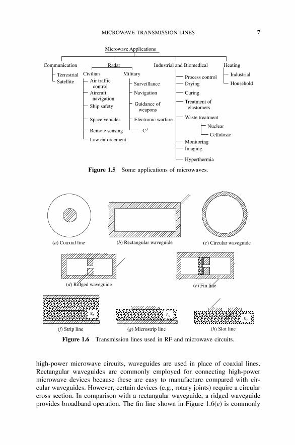
Figure 1.5 lists some applications of microwaves. In addition to terrestrialand satellite communications, microwaves are used in radar systems as wellas in various industrial and medical applications. Civilian applications of radarinclude air traffic control, navigation, remote sensing, and law enforcement. Itsmilitary uses include surveillance; guidance of weapons; and command, control,and communication (C3). Radio-frequency and microwave energy are also usedin industrial heating and for household cooking. Since this process does not use aconduction mechanism for the heat transfer, it can improve the quality of certainproducts significantly. For example, the hot air used in a printing press to dryink affects the paper adversely and shortens the product’s life span. By contrast,in microwave drying only the ink portion is heated, and the paper is barelyaffected. Microwaves are also used in material processing, telemetry, imaging,and hyperthermia.
1.1 MICROWAVE TRANSMISSION LINES
Figure 1.6 shows selected transmission lines used in RF and microwave circuits.The most common transmission line used in the RF and microwave range is the

MICROWAVE TRANSMISSION LINES 5
(a) Signal propagation along the ground
Transmittingantenna
Receivingantenna
Earth
(b) Propagation of a sky wave
Earth
Transmittingantenna
Receiving antenna
Ionosphere
Transmittingantenna
Receivingantenna
Earth
(c) Line-of-sight propagation
Figure 1.2 Modes of signal propagation.
coaxial line. A low-loss dielectric material is used in these transmission lines tominimize signal loss. Semirigid coaxial lines with continuous cylindrical con-ductors outside perform well in the microwave range. To ensure single-modetransmission, the cross section of a coaxial line must be much smaller than thesignal wavelength. However, this limits the power capacity of these lines. In

6 INTRODUCTION
Microwave Devices
ActivePassive
Solid-State Vacuum-Tube
Linear Beam Cross-Field
KlystronsTraveling wave tubesHybrid tubes
Magnetrons
Directional couplersAttenuatorsPhase shiftersAntennasResonators
Figure 1.3 Microwave devices.
Solid-State Devices
Transistors Transferred Electron Avalanche Transit Time Quantum Electronic
BJTFETHEMT
Gunn diodeLSA diodeInP diodeCdTe diode
BARITT diodeIMPATT diodeTRAPATT diodeParametric devices
Ruby masers
Semiconductor laser
Figure 1.4 Solid-state devices used at RF and microwave frequencies.
TABLE 1.4 Selected Applications of Microwave Solid-State Devices
Devices Applications Advantages
Transistors L-band transmitters fortelemetry systems andphased-array radar systems;transmitters forcommunication systems
Low cost, low power supply,reliable, high-continuous-wave (CW) power output,lightweight
Transferred electrondevices (TED)
C-, X-, and Ku-band ECMamplifiers for widebandsystems; X- and Ku-bandtransmitters for radarsystems, such as trafficcontrol
Low power supply (12 V),low cost, lightweight,reliable, low noise, highgain
IMPATT diode Transmitters formillimeter-wavecommunication
Low power supply, low cost,reliable, high-CW power,lightweight
TRAPATT diode S-band pulsed transmitter forphased-array radar systems
High peak and averagepower, reliable, low powersupply, low cost
BARITT diode Local oscillators incommunication and radarreceivers
Low power supply, low cost,low noise, reliable
MICROWAVE TRANSMISSION LINES 7
Microwave Applications
Communication
TerrestrialSatellite
Radar
Civilian Military
Industrial and Biomedical Heating
Industrial
HouseholdAir trafficcontrol
Aircraft navigation
Ship safety
Space vehicles
Remote sensing
Law enforcement
Surveillance
Navigation
Guidance of weapons
Electronic warfare
C3
Process controlDrying
Curing
MonitoringImaging
Hyperthermia
Treatment of elastomers
Waste treatment
Nuclear
Cellulosic
Figure 1.5 Some applications of microwaves.
(e) Fin line (d) Ridged waveguide
εrεr
(f) Strip line (g) Microstrip line (h) Slot line
εr
(a) Coaxial line (b) Rectangular waveguide (c) Circular waveguide
Figure 1.6 Transmission lines used in RF and microwave circuits.
high-power microwave circuits, waveguides are used in place of coaxial lines.Rectangular waveguides are commonly employed for connecting high-powermicrowave devices because these are easy to manufacture compared with cir-cular waveguides. However, certain devices (e.g., rotary joints) require a circularcross section. In comparison with a rectangular waveguide, a ridged waveguideprovides broadband operation. The fin line shown in Figure 1.6(e) is commonly

8 INTRODUCTION
used in the millimeter-wave band. Physically, it resembles a slot line enclosedin a rectangular waveguide.
The transmission lines illustrated in Figure 1.6(f) to (h) are most convenient inconnecting the circuit components on a printed circuit board (PCB). The physicaldimensions of these transmission lines depend on the dielectric constant εr ofinsulating material and on the operating frequency band. The characteristics anddesign formulas of selected transmission lines are given in the appendixes.
1.2 TRANSMITTER AND RECEIVER ARCHITECTURES
Wireless communication systems require a transmitter at one end to send theinformation signal and a receiver at the other to retrieve it. In one-way commu-nication (such as a commercial broadcast), a transmitting antenna radiates thesignal according to its radiation pattern. The receiver, located at the other end,receives this signal via its antenna and extracts the information, as illustrated inFigure 1.7. Thus, the transmitting station does not require a receiver, and viceversa. On the other hand, a transceiver (a transmitter and a receiver) is neededat both ends to establish a two-way communication link.
Figure 1.7 is a simplified block diagram of a one-way communication link. Atthe transmitting end, an information signal is modulated and mixed with a localoscillator to up-convert the carrier frequency. Bandpass filters are used before
Modulator BPF BPF
LO
Up-converter
Poweramplifier
Informationsignal
(a)
Demodulator BPF/IFamp.
Frequency-selectivecircuit
LO
Down-converter
Low-noiseamplifier
Informationsignal BPF
(b)
Figure 1.7 Simplified block diagram of the transmitter (a) and receiver (b) of a wirelesscommunication system.

TRANSMITTER AND RECEIVER ARCHITECTURES 9
and after the mixer to stop undesired harmonics. The signal power is ampli-fied before feeding it to the antenna. At the receiving end the entire process isreversed to recover the information. Signal received by the antenna is filtered andamplified to improve the signal-to-noise ratio before feeding it to the mixer fordown-converting the frequency. A frequency-selective amplifier (tuned amplifier)amplifies it further, before feeding it to a suitable demodulator, which extractsthe information signal.
In an analog communication system, the amplitude or angle (frequency orphase) of the carrier signal is varied according to the information signal. Thesemodulations are known as amplitude modulation (AM), frequency modulation(FM), and phase modulation (PM), respectively. In a digital communication sys-tem, the input passes through channel coding, interleaving, and other processingbefore it is fed to the modulator. Various modulation schemes are available,including on–off keying (OOK), frequency-shift keying (FSK), and phase-shiftkeying (PSK). As these names suggest, a high-frequency signal is turned on andoff in OOK to represent the logic states 1 and 0 of a digital signal. Similarly,two different signal frequencies are employed in FSK to represent the two signalstates. In PSK, the phase of the high-frequency carrier is changed according tothe 1 or 0 state of the signal. If only two phase states (0 and 180) of the carrierare used, it is called binary phase-shift keying (BPSK). On the other hand, aphase shift of 90 gives four possible states, each representing 2 bits of infor-mation (known as a dibit). This type of digital modulation, known as quadraturephase-shift keying (QPSK), is explained further below.
Consider a sinusoidal signal Smod, as given by equation (1.2.1). Its angularfrequency and phase are ω radians per second and φ, respectively:
Smod(t) = √2 cos(ωt − φ) = √
2(cos ωt cos φ + sin ωt sin φ) (1.2.1)
This can be simplified further as follows:
Smod(t) = SI cos ωt + SQ sin ωt (1.2.2)
whereSI = √
2 cos φ (1.2.3)
andSQ = √
2 sin φ (1.2.4)
The subscripts I and Q represent in-phase and quadrature-phase components ofSmod. Table 1.5 shows the values of SI and SQ for four different phase statestogether with the corresponding dibit representations. This scheme can be imple-mented easily for a polar digital signal (positive peak value representing logic 1and the negative peak logic 0). It is illustrated in Figure 1.8. The demultiplexersimultaneously feeds one bit of the digital input SBB to the top and the other tothe bottom branch of this circuit. The top branch multiplies the signal by cos ωt

10 INTRODUCTION
TABLE 1.5 QPSK Scheme
φ SI SQ Dibit Representation
π/4 1 1 113π/4 −1 1 015π/4 −1 −1 007π/4 1 −1 10
I Q
90°Phase shift
Σ
A cos ωt
A sin ωt
LO
Logic 1 = 1 VLogic 0 = −1 V
Logic 1 = 1 VLogic 0 = −1 V
Demultiplexer SBB(t) Smod(t)
Figure 1.8 Block diagram of a QPSK modulation scheme.
I Q
90°Phase shift
A cos ωt
Asin ωt
LO
Multiplexer SBB(t) Smod(t)
Integrator
Integrator Thresholddetector
Thresholddetector
Figure 1.9 Block diagram of a QPSK demodulation scheme.
and the bottom signal by sin ωt . The outputs of the two mixers are then addedto generate Smod.
Demodulation inverts the modulation to retrieve SBB. As illustrated in Figure 1.9,Smod is multiplied by cos ωt in the top branch and by sin ωt in the bottom branch ofthe demodulator. The top integrator stops SQ, and the bottom integrator, SI . Twothreshold detectors generate the corresponding logic states that are multiplexed bythe multiplexer unit to recover SBB. Chapter 2 provides an overview of wirelesscommunication systems and their characteristics.
2COMMUNICATION SYSTEMS
Modern communication systems require RF and microwave signals for the wire-less transmission of information. These systems employ oscillators, mixers, filters,and amplifiers to generate and process various types of signals. The transmittercommunicates with the receiver via antennas placed on each side. Electricalnoise associated with the systems and the channel affects the performance. Asystem designer needs to know about the channel characteristics and systemnoise in order to estimate the required power levels. The chapter begins withan overview of microwave communication systems and RF wireless services toillustrate the applications of circuits and devices that are described in the fol-lowing chapters. It also covers the placement of various building blocks in agiven system.
A short discussion on antennas is included to help in understanding signalbehavior when it propagates from a transmitter to a receiver. The Friis trans-mission formula and the radar range equation are important to understanding theeffects of frequency, range, and operating power levels on the performance of acommunication system. Note that radar concepts now find many other applica-tions, such as proximity or level sensing in an industrial environment. Therefore,a brief discussion of Doppler radar is also included. Noise and distortion charac-teristics play a significant role in analysis and design of these systems. Minimumdetectable signal (MDS), gain compression, intercept point, and the dynamicrange of an amplifier (or receiver) are introduced later. Other concepts associatedwith noise and distortion characteristics are also introduced in this chapter.
Radio-Frequency and Microwave Communication Circuits: Analysis and Design, Second Edition,By Devendra K. MisraISBN 0-471-47873-3 Copyright 2004 John Wiley & Sons, Inc.
11

12 COMMUNICATION SYSTEMS
2.1 TERRESTRIAL COMMUNICATION
As mentioned in Chapter 1, microwave signals propagate along the line of sight.Therefore, the Earth’s curvature limits the range over which a microwave com-munication link can be established. A transmitting antenna sitting on a 25-ft-hightower can typically communicate only up to a distance of about 50 km. Repeaterscan be placed at regular intervals to extend the range. Figure 2.1 is a blockdiagram of a typical repeater.
A repeater system operates as follows. A microwave signal arriving at antennaA works as input to port 1 of a circulator. It is directed to port 2 without loss,assuming that the circulator is ideal. Then it passes through a receiver protectioncircuit that limits the magnitude of large signals but passes those of low intensitywith negligible attenuation. The purpose of this circuit is to block excessivelylarge signals from reaching the receiver input. The mixer following it works as adown-converter that transforms a high-frequency signal to a low-frequency signal,typically in the range of 70 MHz. A Schottky diode is generally employed in themixer because of its superior noise characteristics. This frequency conversionfacilitates amplification of the signal economically. A bandpass filter is used at theoutput of the mixer to stop undesired harmonics. An intermediate-frequency (IF)amplifier is then used to amplify the signal. It is generally a low-noise solid-state
Receiverprotectioncircuit
Poweramplifier
Bandpassfilter
Bandpassfilter
IFamplifierwith AGC
Limitercircuit
Transreceiver for the reverse direction (from B to A)
Transmitter fordirection A
Bandpassfilter
Powerdivider
Microwavesource Shift
oscillator
Mixer
Mixer
Circulator A Circulator B
A Received
fromdirection B
2
1 31 2
3
Mixer
B
Figure 2.1 Block arrangement of a repeater system.

SATELLITE COMMUNICATION 13
amplifier with ultralinear characteristics over a broadband. The amplified signalis mixed with another signal for up-conversion of frequency. After filtering outundesired harmonics introduced by the mixer, it is fed to a power amplifier stagethat feeds circulator B for onward transmission through antenna B. This up-converting mixer circuit generally employs a varactor diode. Circulator B directsthe signal entering at port 3 to the antenna connected at its port 1. Similarly,the signal propagating upstream is received by antenna B and the circulatordirects it toward port 2. It then goes through the processing as described for thedownstream signal and is radiated by antenna A for onward transmission. Hence,the downstream signal is received by antenna A and transmitted in the forwarddirection by antenna B. Similarly, the upstream signal is received by antenna Band forwarded to the next station by antenna A. The two circulators help channelthe signal in the correct direction.
A parabolic antenna with tapered horn as primary feeder is generally used inmicrowave links. This type of composite antenna system, known as a hog horn,is fairly common in high-density links because of its broadband characteristics.These microwave links operate in the frequency range 4 to 6 GHz, and signalspropagating in two directions are separated by a few hundred megahertz. Sincethis frequency range overlaps with C-band satellite communication, the inter-ference of these signals needs to be taken into design consideration. A singlefrequency can be used twice for transmission of information using vertical andhorizontal polarization.
2.2 SATELLITE COMMUNICATION
The ionosphere does not reflect microwaves as it does RF signals. However, onecan place a conducting object (satellite) up in the sky that reflects them back toEarth. A satellite can even improve the signal quality using on-board electronicsbefore transmitting it back. The gravitational force needs to be balanced somehowif this object is to stay in position. An orbital motion provides this balancing force.If a satellite is placed at low altitude, greater orbital force will be needed to keepit in position. These low- and medium-altitude satellites are visible from a groundstation only for short periods. On the other hand, satellites placed at an altitudeof about 36,000 km over the equator, called geosynchronous or geostationarysatellites are visible from their shadows at all times.
C-band geosynchronous satellites use between 5725 and 7075 MHz fortheir uplinks. The corresponding downlinks are between 3400 and 5250 MHz.Table 2.1 lists the downlink center frequencies of a 24-channel transponder. Eachchannel has a total bandwidth of 40 MHz; 36 MHz of that carries the information,and the remaining 4 MHz is used as a guard band. It is accomplished with a500-MHz bandwidth using different polarization for the overlapping frequencies.The uplink frequency plan may be found easily after adding 2225 MHz to thesedownlink frequencies. Figure 2.2 illustrates the simplified block diagram of aC-band satellite transponder. A 6-GHz signal received from the Earth station

14 COMMUNICATION SYSTEMS
TABLE 2.1 C-Band Downlink Transponder Frequencies
Horizontal Polarization Vertical Polarization
Channel Center Frequency (MHz) Channel Center Frequency (MHz)
1 3720 2 37403 3760 4 37805 3800 6 38207 3840 8 38609 3880 10 3900
11 3920 12 394013 3960 14 398015 4000 16 402017 4040 18 406019 4080 20 410021 4120 22 414023 4160 24 4180
Uplink6-GHz signal
BPF BPFLNA
LO
TWTamp.
Downlink4-GHz signal
Mixer
Figure 2.2 Simplified block diagram of a transponder.
is passed through a bandpass filter before amplifying it through a low-noiseamplifier (LNA). It is then mixed with a local oscillator (LO) signal to bringdown its frequency. A bandpass filter that is connected right after the mixerfilters out the unwanted frequency components. This signal is then amplified bya traveling wave tube (TWT) amplifier and transmitted back to Earth.
Another frequency band in which satellite communication has been growingcontinuously is the Ku-band. The geosynchronous Fixed Satellite Service (FSS)generally operates between 10.7 and 12.75 GHz (space to Earth) and 13.75 to14.5 GHz (Earth to space). It offers the following advantages over the C-band:
ž The size of the antenna can be smaller (3 ft or even smaller, with higher-power satellites against 8 to 10 ft for C-band).
ž Because of higher frequencies used in the up- and downlinks, there is nointerference with C-band terrestrial systems.
Since higher-frequency signals attenuate faster while propagating throughadverse weather (rain, fog, etc.), Ku-band satellites suffer from this major

SATELLITE COMMUNICATION 15
drawback. Signals with higher powers may be used to compensate for this loss.Generally, this power is on the order of 40 to 60 W. The high-power directbroadcast satellite (DBS) system uses power amplifiers in the range 100 to 120 W.
The National Broadcasting Company (NBC) has been using the Ku-band todistribute the programming to its affiliates. Also, various news-gathering agen-cies have used this frequency band for some time. Convenience stores, auto partsdistributors, banks, and other businesses have used the very small aperture ter-minal (VSAT) because of its small antenna size (typically, on the order of 3 ftin diameter). It offers two-way satellite communication; usually back to hub orheadquarters. The Public Broadcasting Service (PBS) uses VSATs for exchanginginformation among public schools.
Direct broadcast satellites (DBSs) have been around since 1980, but early DBSventures failed for various reasons. In 1991, Hughes Communications enteredinto the direct-to-home (DTH) television business. DirecTV was formed as aunit of GM Hughes, with DBS-1 launched in December 1993. Its longitudinalorbit is at 101.2W, and it employs a left-handed circular polarization. DBS-2,launched in August 1994 uses a right-handed circular polarization, and its orbitallongitude is at 100.8W. DirecTV employs a digital architecture that can utilizevideo and audio compression techniques. It complies with Motion Picture ExpertsGroup (MPEG)-2. By using compression ratios of 5 to 7, over 150 channels ofprograms are available from the two satellites. These satellites include 120-WTWT amplifiers that can be combined to form eight pairs at 240 W of power.This higher power can also be utilized for high-definition television (HDTV)transmission. Earth-to-satellite link frequency is 17.3 to 17.8 GHz; satellite-to-Earth link frequency uses the 12.2- to 12.7-GHz band. Circular polarization isused because it is less affected by rain than is linear orthogonal polarization.
Several communication services are now available that use low-Earth-orbitsatellites (LEOSs) and medium-Earth-orbit satellites (MEOSs). LEOS altitudesrange from 750 to 1500 km; MEOS systems have an altitude around 10,350 km.These services compete with or supplement cellular systems and geosynchronousEarth-orbit satellites (GEOSs). The GEOS systems have some drawbacks, due tothe large distances involved. They require relatively large powers, and the prop-agation time delay creates problems in voice and data transmissions. The LEOSand MEOS systems orbit Earth faster because of being at lower altitudes, andthese are therefore visible only for short periods. As Table 2.2 indicates, severalsatellites are used in a personal communication system to solve this problem.
Three classes of service can be identified for mobile satellite services:
1. Data transmission and messaging from very small, inexpensive satellites2. Voice and data communications from big LEOSs3. Wideband data transmission
Another application of L-band microwave frequencies (1227.60 and1575.42 MHz) is in global positioning systems (GPSs). A constellation of 24satellites is used to determine a user’s geographical location. Two services

16 COMMUNICATION SYSTEMS
TABLE 2.2 Specifications of Certain Personal Communication Satellites
Iridium (LEO) Globalstar (LEO) Odyssey (MEO)
Number of satellites 66 48 12Altitude (km) 755 1,390 10,370Uplink (GHz) 1.616–1.6265 1.610–1.6265 1.610–1.6265Downlink (GHz) 1.616–1.6265 2.4835–2.500 2.4835–2.500Gateway terminal
uplink (GHz)27.5–30.0 C-band 29.5–30.0
Gateway terminaldownlink (GHz)
18.8–20.2 C-band 19.7–20.2
Average satelliteconnect time (min)
9 10–12 120
Features of handsetModulation QPSK FQPSK QPSKBER 1E-2 (voice) 1E-3 (voice) 1E-3 (voice)
1E-5 (data) 1E-5 (data) 1E-5 (data)Supportable data 4.8 (voice) 1.2–9.6 (voice and data) 4.8 (voice)
rate (kb/s) 2.4 (data) 1.2–9.6 (data)
are available: the standard positioning service (SPS) for civilian use, utilizinga single-frequency course/acquisition (C/A) code, and the precise positioningservice (PPS) for the military, utilizing a dual-frequency P-code (protected).These satellites are at an altitude of 10,900 miles above the Earth, with an orbitalperiod of 12 hours.
2.3 RADIO-FREQUENCY WIRELESS SERVICES
A lot of exciting wireless applications have been reported that use voice and datacommunication technologies. Wireless communication networks consist of micro-cells that connect people with truly global, pocket-size communication devices,telephones, pagers, personal digital assistants, and modems. Typically, a cellularsystem employs a 100-W transmitter to cover a cell 0.5 to 10 miles in radius. Thehandheld transmitter has a power of less than 3 W. Personal communication net-works (PCN/PCS) operate with a 0.01- to 1-W transmitter to cover a cell radiusof less than 450 yards. The handheld transmitter power is typically less than10 mW. Table 2.3 shows the cellular telephone standards of selected systems.
There have been no universal standards set for wireless personal communica-tion. In North America, cordless has been CT-0 (an analog 46/49-MHz standard)and cellular AMPS (Advanced Mobile Phone Service) operating at 800 MHz. Thesituation in Europe has been far more complex; every country has had its ownstandard. Although cordless was nominally CT-0, different countries used theirown frequency plans. This led to a plethora of new standards. These include,

RADIO-FREQUENCY WIRELESS SERVICES 17
TABLE 2.3 Selected Cellular Telephones
Analog CellularPhone Standard Digital Cellular Phone Standard
AMP ETACSNADC(IS-54)
NADC(IS-95) GSM PDC
Freq. range (MHz)Tx 824–849 871–904 824–849 824–849 880–915 940–956
1477–1501Rx 869–894 916–949 869–894 869–894 925–960 810–826
1429–1453Transmitter power
(max.)600 mW 200 mW 1 W
Multiple access FDMA FDMA TDMA/FDM CDMA/FDM TDMA/FDM TDMA/FDMNumber of channels 832 1000 832 20 124 1600Channel spacing
(kHz)30 25 30 1250 200 25
Modulation FM FM π/4 DQPSK QPSK/BPSK GMSK π/4 DQPSKBit rate (kb/s) — — 48.6 1228.8 270.833 42
TABLE 2.4 Selected Cordless Telephones
Analog CordlessPhone Standard Digital Cordless Phone Standard
CT-0CT-1
and CT-1+CT-2
and CT-2+ DECTPHS
(Formerly PHP)
Frequency range(MHz)
46/49 CT-1: 914/960;CT-1+:885–932
CT-1:864–868;CT-2+:930/931;940/941
1880–1900 1895–1918
Transmitterpower (max.)(mW)
— — 10 and 80 250 80
Multiple access FDMA FDMA TDMA/FDM TDMA/FDM TDMA/FDMNumber of
channels10–20 CT-1: 40;
CT-1+: 8040 10 (12 users
per channel)300 (four users
per channels)Channel spacing
(kHz)40 25 100 1728 300
Modulation FM FM GFSK GFSK π/4 DQPSKBit rate (kb/s) — — 72 1152 384
but are not limited to, CT-1, CT-1+, DECT (Digital European Cordless Tele-phone), PHP (Personal Handy Phone in Japan), E-TACS (Extended Total AccessCommunication System in the UK), NADC (North American Digital Cellular),GSM (Global System for Mobile Communication), and PDC (Personal DigitalCellular). Specifications for selected cordless telephones are given in Table 2.4.

18 COMMUNICATION SYSTEMS
2.4 ANTENNA SYSTEMS
Figure 2.3 illustrates some of the antennas that are used in communication sys-tems. These can be categorized into two groups: wire antennas and aperture-typeantennas. Electric dipole, monopole, and the loop antennas belong to the for-mer group; horn, reflector, and lens belong to the latter category. The apertureantennas can be further subdivided into primary and secondary (or passive)antennas. Primary antennas are directly excited by the source and can be usedindependently for transmission or reception of signals. On the other hand, asecondary antenna requires another antenna as its feeder. Horn antennas fall inthe first category, whereas the reflector and lens belong to the second. Var-ious types of horn antennas are commonly used as feeders in reflector andlens antennas.
Electronics
Electronics
(a)
(d )
( f )
(e)
(b) (c)
Transmitter
Transmitter
Figure 2.3 Some commonly used antennas: (a) electric dipole; (b) monopole; (c) loop;(d) pyramidal horn; (e) Cassegrain reflector; (f ) lens.
ANTENNA SYSTEMS 19
When an antenna is energized, it generates two types of electromagnetic fields.Part of the energy stays nearby and part propagates outward. The propagatingsignal represents the radiation fields, while the nonpropagating is reactive (capac-itive or inductive) in nature. Space surrounding the antenna can be divided intothree regions. The reactive fields dominate in the nearby region but are reducedin strength at a faster rate than those associated with the propagating signal. Ifthe largest dimension of an antenna is D and the signal wavelength is λ, reactivefields dominate up to about 0.62
√D3/λ and diminish after 2D2/λ. The region
beyond 2D2/λ is called the far-field (or radiation field) region.Power radiated by an antenna per unit solid angle is known as the radiation
intensity U . It is a far-field parameter that is related to power density (power perunit area) Wrad and distance r as follows:
U = r2Wrad (2.4.1)
Directive Gain and Directivity
If an antenna radiates uniformly in all directions, it is called an isotropic antenna.This is a hypothetical antenna that helps in defining the characteristics of a realone. The directive gain DG is defined as the ratio of radiation intensity due tothe test antenna to that of an isotropic antenna. It is assumed that total radiatedpower remains the same in the two cases. Hence,
DG = U
U0= 4πU
Prad(2.4.2)
where U is the radiation intensity due to the test antenna in watts per unit solidangle, U0 the radiation intensity due to the isotropic antenna in watts per unitsolid angle, and Prad the total power radiated in watts. Since U is a directional-dependent quantity, the directive gain of an antenna depends on the angles θ andφ. If the radiation intensity assumes its maximum value, the directive gain iscalled the directivity D0. That is,
D0 = Umax
U0= 4πUmax
Prad(2.4.3)
Gain of an Antenna
The power gain of an antenna is defined as the ratio of its radiation intensity at apoint to the radiation intensity that results from a uniform radiation of the sameinput power. Hence,
gain = 4πradiation intensity
total input power= 4π
U(θ,φ)
Pin(2.4.4)
Most of the time we deal with relative gain. It is defined as a ratio of the powergain of the test antenna in a given direction to the power gain of a reference

20 COMMUNICATION SYSTEMS
antenna. Both antennas must have the same input power. The reference antennais usually a dipole, horn, or any other antenna whose gain can be calculated oris known. However, the reference antenna is a lossless isotropic radiator in mostcases. Hence,
gain = 4πU(θ, φ)
Pin(lossless isotropic antenna)(2.4.5)
When the direction is not stated, the power gain is usually taken in the directionof maximum radiation.
Radiation Patterns and Half-Power Beam Width
Far-field power distribution at a distance r from the antenna depends on the spa-tial coordinates θ and φ. Graphical representations of these distributions on theorthogonal plane (θ-plane or φ-plane) at a constant distance r from the antennaare called its radiation patterns. Figure 2.4 illustrates the radiation pattern of thevertical dipole antenna with θ. Its φ-plane pattern can be found after rotating itabout the vertical axis. Thus, a three-dimensional picture of the radiation patternof a dipole is doughnut shaped. Similarly, the power distributions of other anten-nas generally show peaks and valleys in the radiation zone. The highest peakbetween the two valleys is known as the main lobe; the others are called sidelobes. The total angle about the main peak over which power is reduced by 50%of its maximum value is called the half-power beam width on that plane.
0
θ
1
r
Figure 2.4 Radiation pattern of a dipole in a vertical (θ) plane.

ANTENNA SYSTEMS 21
The following relations are used to estimate the power gain G and the half-power beam width (HPBW, or simply BW) of an aperture antenna:
G = 4π
λ2Ae = 4π
λ2Aκ (2.4.6)
and
BW(degrees) = 65λ
d(2.4.7)
where Ae is the effective area of radiating aperture in square meters, A its physicalarea (πd2/4 for a reflector antenna dish with diameter d), κ the antenna efficiency(ranges from 0.6 to 0.65), and λ the signal wavelength in meters.
Example 2.1 Calculate the power gain (in decibels) and the half-power beamwidth of a parabolic dish antenna 30 m in diameter that is radiating at 4 GHz.
SOLUTION The signal wavelength and area of the aperture are
λ = 3 × 10⁸
4 × 109= 0.075 m
and
A = πd2
4= π
302
4= 706.8584 m2
Assuming that the aperture efficiency is 0.6, the antenna gain and half-powerbeam width are found as follows:
G = 4π
(0.075)2× 706.8584 × 0.6 = 947,482.09
= 10 log10(947,482.09) = 59.76 ≈ 60 dB
BW = 65 × 0.075
30= 0.1625
Antenna Efficiency
If an antenna is not matched with its feeder, a part of the signal available fromthe source is reflected back. It is considered to be the reflection (or mismatch)loss. The reflection (or mismatch) efficiency is defined as a ratio of power inputto the antenna to that of power available from the source. Since the ratio ofreflected power to that of power available from the source is equal to the squareof the magnitude of the voltage reflection coefficient, the reflection efficiency er
is given byer = 1 − ||2

22 COMMUNICATION SYSTEMS
where
= voltage reflection coefficient = ZA − Z0
ZA + Z0
Here ZA is the antenna impedance and Z0 is the characteristic impedance of thefeeding line.
In addition to mismatch, the signal energy may dissipate in an antenna due toimperfect conductor or dielectric material. These efficiencies are hard to compute.However, the combined conductor and dielectric efficiency ecd can be determinedexperimentally after measuring the input power Pin and the radiated power Prad.It is given as
ecd = Prad
Pin
The overall efficiency eo is a product of the efficiencies above. That is,
eo = erecd (2.4.8)
Example 2.2 A 50- transmission line feeds a lossless one-half-wavelength-long dipole antenna. The antenna impedance is 73 . If its radiation intensity,U(θ,φ), is given as
U = B0 sin3 θ
find the maximum overall gain.
SOLUTION The maximum radiation intensity, Umax, is the B0 value that occursat θ = π/2. Its total radiated power is found as follows:
Prad =∫ 2π
0
∫ π
0B0 sin3 θ sin θ dθ dφ = 3
4π2B0
Hence,
D0 = 4πUmax
Prad= 4πB0
34π2B0
= 16
3π= 1.6977
or
D0(dB) = 10 log10(1.6977)dB = 2.2985 dB
Since the antenna is lossless, the radiation efficiency ecd is unity (0 dB). Itsmismatch efficiency is computed as follows.
The voltage reflection coefficient at its input (it is formulated in Chapter 2) is
= ZA − Z0
ZA + Z0= 73 − 50
73 + 50= 23
123
ANTENNA SYSTEMS 23
Therefore, the mismatch efficiency of the antenna is
er = 1 − (23/123)2 = 0.9650 = 10 log10(0.9650)dB = −0.1546 dB
The overall gain G0 (in decibels) is found as follows:
G0(dB) = 2.2985 − 0 − 0.1546 = 2.1439 dB
Bandwidth
Antenna characteristics such as gain, radiation pattern, impedance, and so on arefrequency dependent. The bandwidth of an antenna is defined as the frequencyband over which its performance with respect to some characteristic (HPBW,directivity, etc.) conforms to a specified standard.
Polarization
Polarization of an antenna is the same as polarization of its radiating wave.It is a property of the electromagnetic wave describing the time-varying direc-tion and relative magnitude of an electric field vector. The curve traced by theinstantaneous electric field vector with time is the polarization of that wave. Thepolarization is classified as follows:
ž Linear polarization. If the tip of the electric field intensity traces a straightline in some direction with time, the wave is linearly polarized.
ž Circular polarization. If the end of the electric field traces a circle in spaceas time passes, that electromagnetic wave is circularly polarized. Further, itmay be right-handed circularly polarized (RHCP) or left-handed circularlypolarized (LHCP), depending on whether the electric field vector rotatesclockwise or counterclockwise.
ž Elliptical polarization. If the tip of the electric field intensity traces an ellipsein space as time lapses, the wave is elliptically polarized. As in the pre-ceding case, it may be right- or left-handed elliptical polarization (RHEPand LHEP).
In a receiving system, the polarization of the antenna and the incoming waveneed to be matched for maximum response. If this is not the case, there will besome signal loss, known as polarization loss. For example, if there is a verticallypolarized wave incident on a horizontally polarized antenna, the induced voltageavailable across its terminals will be zero. In this case, the antenna is cross-polarized with an incident wave. The square of the cosine of the angle betweenwave polarization and antenna polarization is a measure of the polarization loss.It can be determined by squaring the scalar product of unit vectors representingthe two polarizations.

24 COMMUNICATION SYSTEMS
Example 2.3 The electric field intensity of an electromagnetic wave propagat-ing in a lossless medium in the z-direction is given by
E(r, t) = xE0(x, y) cos(ωt − kz) V/m
It is incident upon an antenna that is linearly polarized as follows:
Ea(r) = (x + y)E(x, y, z) V/m
Find the polarization loss factor.
SOLUTION In this case, the incident wave is linearly polarized along the x-axiswhile the receiving antenna is linearly polarized at 45 from it. Therefore, one-half of the incident signal is cross-polarized with the antenna. It is determinedmathematically as follows. The unit vector along the polarization of incidentwave is
ui = x
The unit vector along the antenna polarization may be found as
ua = 1√2(x + y)
Hence, the polarization loss factor is
|ui•ua|2 = 0.5 = −3.01 dB
Effective Isotropic Radiated Power
The effective isotropic radiated power (EIRP) is a measure of the power gain ofthe antenna. It is equal to the power needed by an isotropic antenna that providesthe same radiation intensity at a given point as that of the directional antenna.If power input to the feeding line is Pt and the antenna gain is Gt , the EIRP isdefined as
EIRP = PtGt
L(2.4.9)
where L is the input/output power ratio of the transmission line that is connectedbetween the output of the final power amplifier stage of the transmitter and theantenna. It is given by
L = Pt
Pant(2.4.10)
Alternatively, the EIRP can be expressed in dBw as
EIRP(dBw) = Pt(dBw) − L(dB) + G(dB) (2.4.11)

ANTENNA SYSTEMS 25
Example 2.4 In a transmitting system, the output of the final high-power ampli-fier is 500 W, and the line feeding its antenna has an attenuation of 20%. If thegain of the transmitting antenna is 60 dB, find the EIRP in dBw.
SOLUTION
Pt = 500 W = 26.9897 dBw
Pant = 0.8 × 500 = 400 W
G = 60 dB = 106
and
L = 500
400= 1.25 = 10 log10(1.25) = 0.9691 dB
Hence,
EIRP(dBw) = 26.9897 − 0.9691 + 60 = 86.0206 dBw
or
EIRP = 500 × 106
1.25= 400 × 106 W
Space Loss
The transmitting antenna radiates in all directions, depending on its radiationcharacteristics. However, the receiving antenna receives only the power that isincident on it. Hence, the rest of the power is not used and is lost in space. It isrepresented by the space loss. It can be determined as follows.
The power density wt of a signal transmitted by an isotropic antenna isgiven by
wt = Pt
4πR2W/m2 (2.4.12)
where Pt is the transmitted power in watts and R is the distance from the antennain meters. The power received by a unity-gain antenna located at R is found to be
Pr = wtAeu (2.4.13)
where Aeu is the effective area of an isotropic antenna.From (2.4.6), for an isotropic antenna,
G = 4π
λ2Aeu = 1
or
Aeu = λ2
4π

26 COMMUNICATION SYSTEMS
Hence, (2.4.12) can be written as
Pr = Pt
4πR2
λ2
4π(2.4.14)
and the space loss ratio is found to be
Pr
Pt
=(
λ
4πR
)2
(2.4.15)
It is usually expressed in decibels as follows:
space loss ratio = 20 log10λ
4πRdB (2.4.16)
Example 2.5 A geostationary satellite is 35,860 km away from Earth’s surface.Find the space loss ratio if it is operating at 4 GHz.
SOLUTION
R = 35,860,000 m and λ = 3 × 10⁸
4 × 109= 0.075 m
Hence,
space loss ratio =(
4π × 35,860,000
0.075
)2
= 2.77 × 10−20 = −195.5752 dB
Friis Transmission Formula and Radar Range Equation
Analysis and design of communication and monitoring systems often require anestimation of transmitted and received powers. The Friis transmission formulaand radar range equation provide the means for such calculations. The former isapplicable to a one-way communication system where the signal is transmittedat one end and is received at the other end of the link. The radar range equationis applicable when the signal transmitted hits a target and the signal reflectedis generally received at the location of the transmitter. We consider these twoformulations next.
Friis Transmission Equation
Consider a simplified communication link as illustrated in Figure 2.5. A distanceR separates the transmitter and the receiver. Effective apertures of transmittingand receiving antennas are Aet and Aer , respectively. Further, the two antennas
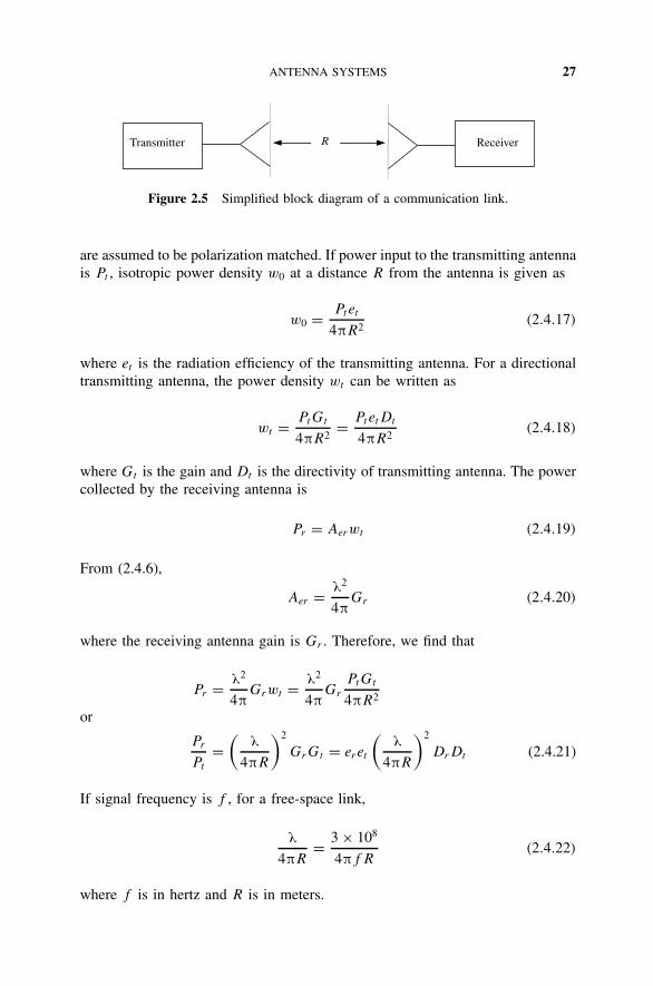
ANTENNA SYSTEMS 27
R Transmitter Receiver
Figure 2.5 Simplified block diagram of a communication link.
are assumed to be polarization matched. If power input to the transmitting antennais Pt , isotropic power density w0 at a distance R from the antenna is given as
w0 = Ptet
4πR2(2.4.17)
where et is the radiation efficiency of the transmitting antenna. For a directionaltransmitting antenna, the power density wt can be written as
wt = PtGt
4πR2= PtetDt
4πR2(2.4.18)
where Gt is the gain and Dt is the directivity of transmitting antenna. The powercollected by the receiving antenna is
Pr = Aerwt (2.4.19)
From (2.4.6),
Aer = λ2
4πGr (2.4.20)
where the receiving antenna gain is Gr . Therefore, we find that
Pr = λ2
4πGrwt = λ2
4πGr
PtGt
4πR2
or
Pr
Pt
=(
λ
4πR
)2
GrGt = eret
(λ
4πR
)2
DrDt (2.4.21)
If signal frequency is f , for a free-space link,
λ
4πR= 3 × 10⁸
4πf R(2.4.22)
where f is in hertz and R is in meters.

28 COMMUNICATION SYSTEMS
Generally, the link distance is long and the signal frequency is high, such thatkilometer and megahertz will be more convenient units than the usual meter andhertz, respectively. For R in kilometers and f in megahertz, we find that
λ
4πR= 3 × 10⁸
4π × 106fMHz × 103Rkm= 0.3
4π
1
fMHzRkm(2.4.23)
Hence, from (2.4.21),
Pr(dBm) = Pt(dBm) + 20 log100.3
4π− 20 log10(fMHzRkm) + Gt(dB) + Gr(dB)
or
Pr(dBm) = Pt(dBm) + Gt(dB) + Gr(dB) − 20 log10(fMHzRkm) − 32.4418
(2.4.24)where the power transmitted and the power received are in dBm while the twoantenna gains are in decibels.
Example 2.6 A 20-GHz transmitter on board the satellite uses a parabolicantenna that is 45.7 cm in diameter. The antenna gain is 37 dB and its radi-ated power is 2 W. The ground station that is 36,941.031 km away from it hasan antenna gain of 45.8 dB. Find the power collected by the ground station. Howmuch power would be collected at the ground station if there were isotropicantennas on both sides?
SOLUTION The power transmitted, Pt (dBm) = 10 log10(2000)=33.0103 dBmand
20 log10(fMHzRkm) = 20 log10(20 × 103 × 36,941.031) = 177.3708 dB
Hence, the power received at the Earth station is found as follows:
Pr(dBm) = 33.0103 + 37 + 45.8 − 177.3708 − 32.4418 = −94.0023 dBm
or
Pr = 3.979 × 10⁻¹⁰ mW
If the two antennas are isotropic, Gt = Gr = 1 (or 0 dB) and therefore
Pr (dBm) = 33.0103 + 0 + 0 − 177.3708 − 32.4418 = −176.8023 dBm
or
Pr = 2.0882 × 10⁻¹⁸ mW

ANTENNA SYSTEMS 29
Radar Equation
In the case of a radar system, the signal transmitted is scattered by the targetin all possible directions. The receiving antenna collects part of the energy thatis scattered back toward it. Generally, a single antenna is employed for boththe transmitter and the receiver, as shown in Fig. 2.6. If power input to thetransmitting antenna is Pt and its gain is Gt , the power density winc incident onthe target is
winc = PtGt
4πR2= PtAet
λ2R2(2.4.25)
where Aet is the effective aperture of the transmitting antenna.The radar cross section σ of an object is defined as the area intercepting that
amount of power that when scattered isotropically produces at the receiver apower density that is equal to that scattered by the actual target. Hence,
radar cross section = scattered power
incident power densitysquare meters
or
σ = 4πr2 wr
winc(2.4.26)
where wr is isotropically backscattered power density at a distance r and winc ispower density incident on the object. Hence, the radar cross section of an objectis its effective area that intercepts an incident power density winc and gives anisotropically scattered power of 4πr2wr for a backscattered power density. Radarcross sections of selected objects are listed in Table 2.5.
Using the radar cross section of a target, the power intercepted by it can befound as follows:
Pinc = σwinc = σPtGt
4πR2(2.4.27)
Power density arriving back at the receiver is
wscatter = Pinc
4πR2(2.4.28)
Transmitter
Receiver AntennaCirculator
Figure 2.6 Radar system.

30 COMMUNICATION SYSTEMS
TABLE 2.5 Radar Cross Sections of Selected Objects
Object Radar Cross Section (m2)
Pickup truck 200Automobile 100Jumbo-jet airliner 100Large bomber 40Large fighter aircraft 6Small fighter aircraft 2Adult male 1Conventional winged missile 0.5Bird 0.01Insect 0.00001Advanced tactical fighter 0.000001
and power available at the receiver input is
Pr = Aerwscatter = Grλ2σPtGt
4π(4πR2)2= σAerAetPt
4πλ2R4(2.4.29)
Example 2.7 A distance of 100λ separates two lossless X-band horn antennas(Figure 2.7). Reflection coefficients at the terminals of transmitting and receivingantennas are 0.1 and 0.2, respectively. Maximum directivities of the transmittingand receiving antennas are 16 and 20 dB, respectively. Assuming that the inputpower in a lossless transmission line connected to the transmitting antenna is2 W and that the two antennas are aligned for maximum radiation between themand are polarization matched, find the power input to the receiver.
SOLUTION As discussed in Chapter 3, impedance discontinuity generates anecho signal very similar to that of an acoustical echo. Hence, signal power avail-able beyond the discontinuity is reduced. The ratio of the reflected signal voltageto that of the incident is called the reflection coefficient. Since the power isproportional to the square of the voltage, the power reflected from the disconti-nuity is equal to the square of the reflection coefficient times the incident power.
100l
Pt = [1 − |Γ|2]PS
Pd = [1 − |Γ|2]PR
ReceiverTransmitter
Figure 2.7 Setup for Example 2.7.

ANTENNA SYSTEMS 31
Therefore, power transmitted in the forward direction will be given by
Pt = (1 − ||2)Pin
and the power radiated by the transmitting antenna is found to be
Pt = (1 − 0.12)2 = 1.98 W
Since the Friis transmission equation requires the antenna gain as a ratio insteadof in decibels, Gt and Gr are calculated as follows:
Gt = 16 dB = 101.6 = 39.8107 and Gr = 20 dB = 102.0 = 100
Hence, from (2.4.21),
Pr =(
λ
4π × 100λ
)2
× 100 × 39.8107 × 1.98
or
Pr = 5 mW
and power delivered to the receiver, Pd , is
Pd = (1 − 0.22)5 = 4.8 mW
Example 2.8 Radar operating at 12 GHz transmits 25 kW through an antennaof 25 dB gain. A target with its radar cross section at 8 m2 is located at 10 kmfrom the radar. If the same antenna is used for the receiver, determine thepower received.
SOLUTION
Pt = 25 kW
f = 12 GHz → λ = 3 × 10⁸
12 × 109= 0.025 m
Gr = Gt = 25 dB → 102.5 = 316.2278
R = 10 km σ = 8 m2
Hence,
Pr = GrGtPtσλ2
4π(4πR2)2= 316.22782 × 25, 000 × 8 × 0.0252
(4π)3(104)4= 6.3 × 10⁻¹³ W
or
Pr = 0.63 pW
32 COMMUNICATION SYSTEMS
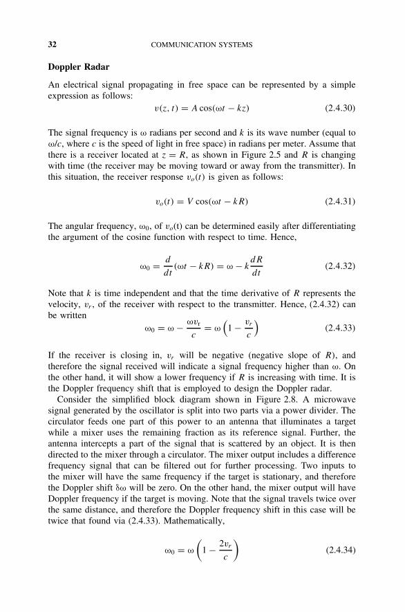
Doppler Radar
An electrical signal propagating in free space can be represented by a simpleexpression as follows:
v(z, t) = A cos(ωt − kz) (2.4.30)
The signal frequency is ω radians per second and k is its wave number (equal toω/c, where c is the speed of light in free space) in radians per meter. Assume thatthere is a receiver located at z = R, as shown in Figure 2.5 and R is changingwith time (the receiver may be moving toward or away from the transmitter). Inthis situation, the receiver response vo(t) is given as follows:
vo(t) = V cos(ωt − kR) (2.4.31)
The angular frequency, ω0, of vo(t) can be determined easily after differentiatingthe argument of the cosine function with respect to time. Hence,
ω0 = d
dt(ωt − kR) = ω − k
dR
dt(2.4.32)
Note that k is time independent and that the time derivative of R represents thevelocity, vr , of the receiver with respect to the transmitter. Hence, (2.4.32) canbe written
ω0 = ω − ωvr
c= ω
(1 − vr
c
)(2.4.33)
If the receiver is closing in, vr will be negative (negative slope of R), andtherefore the signal received will indicate a signal frequency higher than ω. Onthe other hand, it will show a lower frequency if R is increasing with time. It isthe Doppler frequency shift that is employed to design the Doppler radar.
Consider the simplified block diagram shown in Figure 2.8. A microwavesignal generated by the oscillator is split into two parts via a power divider. Thecirculator feeds one part of this power to an antenna that illuminates a targetwhile a mixer uses the remaining fraction as its reference signal. Further, theantenna intercepts a part of the signal that is scattered by an object. It is thendirected to the mixer through a circulator. The mixer output includes a differencefrequency signal that can be filtered out for further processing. Two inputs tothe mixer will have the same frequency if the target is stationary, and thereforethe Doppler shift δω will be zero. On the other hand, the mixer output will haveDoppler frequency if the target is moving. Note that the signal travels twice overthe same distance, and therefore the Doppler frequency shift in this case will betwice that found via (2.4.33). Mathematically,
ω0 = ω
(1 − 2vr
c
)(2.4.34)

NOISE AND DISTORTION 33
Oscillator
Amplifier
Mixer
Display
Circulator
Power divider
ω
ω ω
ω0
ω0
δω
Figure 2.8 Simplified block diagram of a Doppler radar.
and
δω = 2ωvr
c(2.4.35)
2.5 NOISE AND DISTORTION
Random movement of charges or charge carriers in an electronic device generatescurrents and voltages that vary randomly with time. In other words, the amplitudeof these electrical signals cannot be predicted at any time. However, it can beexpressed in terms of probability density functions. These signals are termednoise. For most applications it suffices to know the mean-square or root-mean-square value. Since the square of the current or the voltage is proportional to thepower, mean-square noise voltage and current values are generally called noisepower. Further, noise power is normally a function of frequency and the powerper unit frequency (watts per hertz) is defined as the power spectral density ofnoise. If the noise power is the same over the entire frequency band of interest,it is called white noise. There are several mechanisms that can cause noise in anelectronic device. Some of these are as follows:
ž Thermal noise. This is the most basic type of noise, which is caused bythermal vibration of bound charges. Johnson studied this phenomenon in1928, and Nyquist formulated an expression for spectral density around thesame time. Therefore, it is also known as Johnson noise or Nyquist noise.In most electronic circuits, thermal noise dominates; therefore, it will bedescribed further because of its importance.
ž Shot noise. This is due to random fluctuations of charge carriers that passthrough the potential barrier in an electronic device. For example, electrons

34 COMMUNICATION SYSTEMS
emitted from the cathode of thermionic devices or charge carriers in Schottkydiodes produce a current that fluctuates about the average value I . Themean-square current due to shot noise is generally given by
〈i2Sh〉 = 2eIB (2.5.1)
where e is electronic charge (1.602 × 10⁻¹⁹ C) and B is the bandwidthin hertz.
ž Flicker noise. This occurs in solid-state devices and vacuum tubes operatingat low frequencies. Its magnitude decreases with an increase in frequency.It is generally attributed to chaos in the dynamics of a system. Since theflicker noise power varies inversely with frequency, it is often called 1/fnoise. Sometimes it is referred to as pink noise.
Thermal Noise
Consider a resistor R that is at a temperature of T Kelvin. Electrons in this resistorare in random motion with a kinetic energy that is proportional to the temperatureT . These random motions produce small, random voltage fluctuations across itsterminals. This voltage has a zero average value but a nonzero mean-square value〈v2
n〉. It is given by Planck’s blackbody radiation law as
〈v2n〉 = 4hfRB
exp(hf/kT ) − 1(2.5.2)
where h is Planck’s constant (6.546 × 10⁻³⁴ J · s), k the Boltzmann constant(1.38 × 10⁻²³ J/K), T the temperature in kelvin, B the system bandwidth in hertz,and f the center frequency of the bandwidth in hertz.
For frequencies below 100 GHz, the product hf will be smaller than 6.546 ×10⁻²³ J and kT will be greater than 1.38 × 10⁻²² J if T stays above 10 K. There-fore, kT will be larger than hf for such cases. Hence, the exponential term inequation (2.5.2) can be approximated as follows:
exp
(hf
kT
)≈ 1 + hf
kT
Therefore,
〈v2n〉 ≈ 4hfRB
hf/kT= 4BRkT (2.5.3)
This is known as the Rayleigh–Jeans approximation.A Thevenin-equivalent circuit can replace the noisy resistor as shown in
Figure 2.9. As illustrated, it consists of a noise-equivalent voltage source in serieswith a noise-free resistor. This source will supply a maximum power to a load

NOISE AND DISTORTION 35
R
R
Noisy resistor
Noise-free resistor
<vn2>
Figure 2.9 Noise-equivalent circuit of a resistor.
of resistance R. The power delivered to that load in a bandwidth B is foundas follows:
Pn = 〈v2n〉
4R= kT B (2.5.4)
Conversely, if an arbitrary white noise source with its driving point impedanceR delivers a noise power Ps to a load R, it can be represented by a noisy resistorof value R that is at temperature Te. Hence,
Te = Ps
kB(2.5.5)
where Te is an equivalent temperature selected so that the same noise power isdelivered to the load.
Consider the noisy amplifier as shown in Figure 2.10. Its gain is G over thebandwidth B. Let the amplifier be matched to the noiseless source and the loadresistors. If the source resistor is at a hypothetical temperature of Ts = 0 K, thepower input to the amplifier Pi will be zero and the output noise power Po willonly be due to noise generated by the amplifier. We can obtain the same noisepower at the output of an ideal noiseless amplifier by raising the temperature Ts
of the source resistor to Te:
Te = Po
GkB(2.5.6)
Hence, the output power in both cases is Po = GkTeB. The temperature Te isknown as the equivalent noise temperature of the amplifier.
Noisyamplifier
R Ts = 0 K
R R
R GkB
PoTe = Noiselessamplifier
Figure 2.10 Noise-equivalent representation of an amplifier.

36 COMMUNICATION SYSTEMS
Measurement of Noise Temperature by the Y -Factor Method
According to the definition, the noise temperature of an amplifier (or any othertwo-port network) can be determined by setting the source resistance R at 0 K andthen measuring the output noise power. However, a temperature of 0 K cannot beachieved in practice. We can circumvent this problem by repeating the experimentat two different temperatures. This procedure is known as the Y-factor method.
Consider an amplifier with a power gain of G over a frequency band of B
hertz. Further, its equivalent noise temperature is Te(K). The input port of theamplifier is terminated by a matched resistor R while a matched power meter isconnected at its output, as illustrated in Figure 2.11. With R at temperature Th,the power meter measures the noise output as P1. Similarly, the noise power isfound to be P2 when the temperature of R is set at Tc. Hence,
P1 = GkThB + GkTeB
and
P2 = GkTcB + GkTeB
For Th higher than Tc, the noise power P1 will be larger than P2. Therefore,
P1
P2= Y = Th + Te
Tc + Te
or
Te = Th − YTc
Y − 1(2.5.7)
For Th larger than Tc, Y will be greater than unity. Further, measurement accuracyis improved by selecting two temperature settings that are far apart. Therefore,Th and Tc represent hot and cold temperatures, respectively.
Example 2.9 An amplifier has a power gain of 10 dB in the 500-MHz to 1.5-GHz frequency band. The following data are obtained for this amplifier using the
P1
P2
G, B, Te
Amplifier
Th
Tc
R
R
Figure 2.11 Experimental setup for measurement of noise temperature.
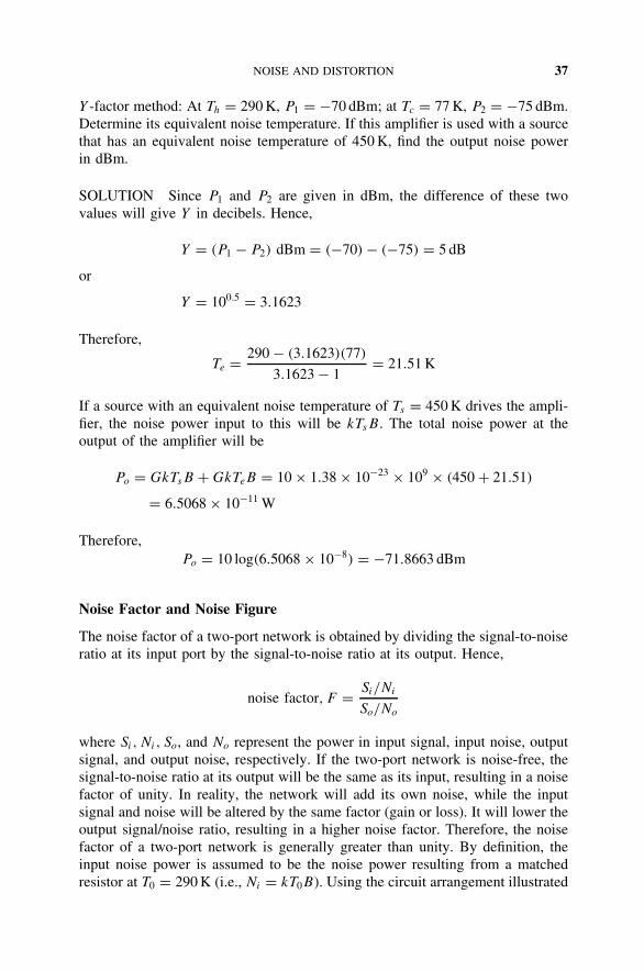
NOISE AND DISTORTION 37
Y -factor method: At Th = 290 K, P1 = −70 dBm; at Tc = 77 K, P2 = −75 dBm.Determine its equivalent noise temperature. If this amplifier is used with a sourcethat has an equivalent noise temperature of 450 K, find the output noise powerin dBm.
SOLUTION Since P1 and P2 are given in dBm, the difference of these twovalues will give Y in decibels. Hence,
Y = (P1 − P2) dBm = (−70) − (−75) = 5 dB
or
Y = 100.5 = 3.1623
Therefore,
Te = 290 − (3.1623)(77)
3.1623 − 1= 21.51 K
If a source with an equivalent noise temperature of Ts = 450 K drives the ampli-fier, the noise power input to this will be kTsB. The total noise power at theoutput of the amplifier will be
Po = GkTsB + GkTeB = 10 × 1.38 × 10−23 × 109 × (450 + 21.51)
= 6.5068 × 10⁻¹¹ W
Therefore,Po = 10 log(6.5068 × 10⁻⁸) = −71.8663 dBm
Noise Factor and Noise Figure
The noise factor of a two-port network is obtained by dividing the signal-to-noiseratio at its input port by the signal-to-noise ratio at its output. Hence,
noise factor, F = Si/Ni
So/No
where Si, Ni, So, and No represent the power in input signal, input noise, outputsignal, and output noise, respectively. If the two-port network is noise-free, thesignal-to-noise ratio at its output will be the same as its input, resulting in a noisefactor of unity. In reality, the network will add its own noise, while the inputsignal and noise will be altered by the same factor (gain or loss). It will lower theoutput signal/noise ratio, resulting in a higher noise factor. Therefore, the noisefactor of a two-port network is generally greater than unity. By definition, theinput noise power is assumed to be the noise power resulting from a matchedresistor at T0 = 290 K (i.e., Ni = kT0B). Using the circuit arrangement illustrated

38 COMMUNICATION SYSTEMS
T0 = 290 K
Pi = Si + Ni Po = So + No
R
RNoisy two-port
networkG, B, Te
Figure 2.12 Circuit arrangement for determination of the noise factor of a noisytwo-port network.
in Figure 2.12, the noise factor of a noisy two-port network can be definedas follows:
noise factor = total output noise in B when input source temperature is 290 K
output noise of source (only) at 290 K
or
F = kT0BG + Pint
kT0BG= 1 + Pint
kT0BG(2.5.8)
where Pint represents the output noise power that is generated by the two-portnetwork internally. It can be expressed in terms of noise factor as follows:
Pint = k(F − 1)T0BG = kTeBG (2.5.9)
where Te is known as the equivalent noise temperature of a two-port network. Itis related to the noise factor as follows:
Te = (F − 1)T0 (2.5.10)
When the noise factor is expressed in decibels, it is commonly called the noisefigure (NF). Hence,
NF = 10 log10 F dB (2.5.11)
Example 2.10 The power gain of an amplifier is 20 dB in the frequency band10 to 12 GHz. If its noise figure is 3.5 dB, find the output noise power in dBm.
SOLUTION
Output noise power = kT0BG + Pint = FkT0BG = No
F = 3.5 dB = 100.35 = 2.2387
G = 20 dB = 102 = 100
Therefore,
No = 2.2387 × 1.38 × 10−23 × 290 × 2 × 109 × 100 = 1.7919 × 10⁻⁹ W
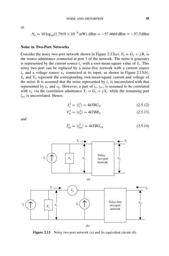
NOISE AND DISTORTION 39
or
No = 10 log10(1.7919 × 10⁻⁶ mW) dBm = −57.4669 dBm ≈ −57.5 dBm
Noise in Two-Port Networks
Consider the noisy two-port network shown in Figure 2.13(a). Ys = Gs + jBs isthe source admittance connected at port 1 of the network. The noise it generatesis represented by the current source is with a root-mean-square value of Is . Thisnoisy two-port can be replaced by a noise-free network with a current sourcein and a voltage source vn connected at its input, as shown in Figure 2.13(b).In and Vn represent the corresponding root-mean-square current and voltage ofthe noise. It is assumed that the noise represented by is is uncorrelated with thatrepresented by in and vn. However, a part of in, inc, is assumed to be correlatedwith vn via the correlation admittance Yc = Gc + jXc while the remaining partinu is uncorrelated. Hence,
I 2s = 〈i2
s 〉 = 4kTBGS (2.5.12)
V 2n = 〈v2
n〉 = 4kTBRn (2.5.13)
and
I 2nu = 〈i2
nu〉 = 4kTBGnu (2.5.14)
(a)
I1 I2
Is ↑ Ys
Noisytwo-portnetwork
V1 V2
(b)
I1 I2
IsIn↑ ↑Ys
V1V2
Noise-freetwo-portnetwork
Vn
Figure 2.13 Noisy two-port network (a) and its equivalent circuit (b).

40 COMMUNICATION SYSTEMS
Now we find a Norton equivalent for the circuit that is connected at the input ofthe noise-free two-port network shown in Figure 2.13(b). Since these are randomvariables, the mean-square noise current < i2
eq > is found as follows:
〈i2eq〉 = 〈i2
s 〉 + 〈|in + Ysvn|2〉 = 〈i2s 〉 + 〈|inu + inc + Ysvn|2〉
= 〈i2s 〉 + 〈|inu + (Yc + Ys)vn|2〉
or
〈i2eq〉 = 〈i2
s 〉 + 〈i2nu〉 + |Yc + Yn|2〈v2
n〉 (2.5.15)
Hence, the noise factor F is
F = 〈i2eq〉
〈i2s 〉
= 1 + 〈i2nu〉
〈i2s 〉
+ |Yc + Ys |2 〈v2n〉
〈i2s 〉
= 1 + Gnu
Gs
+ |Yc + Ys |2 Rn
Gs
or
F = 1 + Gnu
Gs
+ Rn
Gs
[(Gs + Gc)2 + (Xs + Xc)
2] (2.5.16)
For a minimum noise factor, Fmin,
∂F
∂Gs
= 0 ⇒ G2s = G2
c + Gnu
Rn
= G2opt (2.5.17)
and∂F
∂Xs
= 0 ⇒ Xs = −Xc = Xopt (2.5.18)
From (2.5.17),Gnu = Rn(G
2opt − G2
c) (2.5.19)
Substituting (2.5.18) and (2.5.19) into (2.5.16), the minimum noise factor isfound as
Fmin = 1 + 2Rn(Gopt + Gc) (2.5.20)
Using (2.5.18) to (2.5.20), (2.5.16) can be expressed as
F = Fmin + Rn
Gs
|Ys − Yopt|2 (2.5.21)
Noise Figure of a Cascaded System
Consider a two-port network with gain G1, noise factor F1, and equivalent noisetemperature Te1. It is connected in cascade with another two-port network, asshown in Figure 2.14(a). The second two-port network has gain G2, noise factor
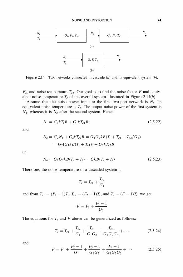
NOISE AND DISTORTION 41
(a)
(b)
Ti
Ni G1, F1, Te1 G2, F2, Te2N1
No
Ti
NiNo
G, F, Te
Figure 2.14 Two networks connected in cascade (a) and its equivalent system (b).
F2, and noise temperature Te2. Our goal is to find the noise factor F and equiv-alent noise temperature Te of the overall system illustrated in Figure 2.14(b).
Assume that the noise power input to the first two-port network is Ni . Itsequivalent noise temperature is Ti . The output noise power of the first system isN1, whereas it is No after the second system. Hence,
N1 = G1kTiB + G1kTe1B (2.5.22)
and
No = G2N1 + G2kTe2B = G1G2kB(Ti + Te1 + Te2/G1)
= G2[G1kB(Ti + Te1)] + G2kTe2B
or
No = G1G2kB(Te + Ti) = GkB(Te + Ti) (2.5.23)
Therefore, the noise temperature of a cascaded system is
Te = Te1 + Te2
G1
and from Te1 = (F1 − 1)Ti, Te2 = (F2 − 1)Ti , and Te = (F − 1)Ti , we get
F = F1 + F2 − 1
G1
The equations for Te and F above can be generalized as follows:
Te = Te1 + Te2
G1+ Te3
G1G2+ Te4
G1G2G3+ · · · (2.5.24)
and
F = F1 + F2 − 1
G1+ F3 − 1
G1G2+ F4 − 1
G1G2G3+ · · · (2.5.25)

42 COMMUNICATION SYSTEMS
Example 2.11 A receiving antenna is connected to an amplifier through a trans-mission line that has an attenuation of 2 dB. The gain of the amplifier is 15 dB, andits noise temperature is 150 K over a bandwidth of 100 MHz. All the componentsare at an ambient temperature of 300 K.
(a) Find the noise figure of this cascaded system.(b) What would be the noise figure if the amplifier were placed before the
transmission line?
SOLUTION First we need to determine the noise factor of the transmission linealone. The formulas derived in the preceding section can then provide the noisefigures desired for the two cases. Consider a transmission line that is match-terminated at both its ends by resistors R0, as illustrated in Figure 2.15. Sincethe entire system is in thermal equilibrium at T (K), noise powers delivered tothe transmission line and available at its output are kTB. Mathematically,
Po = kTB = GkTB + GN added
where Nadded is noise generated by the line as it appears at its input terminals.G is an output-to-input power ratio and B is the bandwidth of the transmissionline. Note that input noise is attenuated in a lossy transmission line, but there isnoise generated by it as well. Hence,
Nadded = 1
G(1 − G)kTB =
(1
G− 1
)kTB = kTeB
An expression for the equivalent noise temperature Te of the transmission line isfound from it as follows:
Te =(
1
G− 1
)T
and
F = 1 + Te
T0= 1 +
(1
G− 1
)T
T0
The gain of the amplifier, Gamp = 15 dB = 101.5 = 31.6228. For the transmissionline, 1/G = 100.2 = 1.5849. Hence, the noise factor of the line is 1 + (1.5849 −1)300/290 = 1.6051. The corresponding noise figure is 2.05 dB. Similarly, the
TR0
TR0
kTBPo = kTB
G, T, R0
Figure 2.15 Lossy transmission line that is matched terminated at its ends.

NOISE AND DISTORTION 43
noise factor of the amplifier is found to be 1 + 150/290 = 1.5172. Its noise figureis 1.81 dB.
(a) In this case the noise figure of the cascaded system, Fcascaded, is found as
Fcascaded = Fline + Famp − 1
Gline= 1.6051 + 1.5172 − 1
1/1.5849= 2.4248 = 3.8468 dB
(b) If the amplifier is connected before the line (i.e., the amplifier is placedright at the antenna),
Fcascaded = Famp + Fline − 1
Gamp= 1.5172 + 1.6051 − 1
31.6228= 1.5363 = 1.8649 dB
Note that the amplifier alone has a noise figure of 1.81 dB. Hence, the noisytransmission line connected after it does not alter the noise figure significantly.
Example 2.12 Two amplifiers, each with a 20-dB gain, are connected in cascadeas shown in Figure 2.16. The noise figure of amplifier A1 is 3 dB, while that ofA2 is 5 dB. Calculate the overall gain and noise figure for this arrangement. If theorder of two amplifiers is changed in the system, find its resulting noise figure.
SOLUTION The noise factors and gains of two amplifiers are
F1 = 3 dB = 100.3 = 2
F2 = 5 dB = 100.5 = 3.1623
G1 = G2 = 20 dB = 102 = 100
Therefore, the overall gain and noise figure of the cascaded system is foundas follows:
G = P3
P1= P3
P2× P2
P1= 100 × 100 = 10, 000 = 40 dB
and
F = F1 + F2 − 1
G1= 2 + 3.1623 − 1
100= 2.021623 = 3.057 dB
P1 P2 P3
A1 A2
Figure 2.16 Setup for Example 2.12.
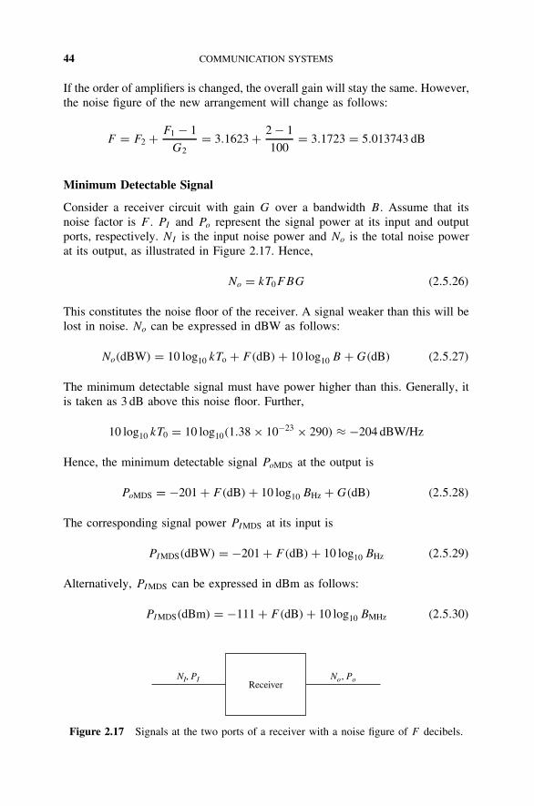
44 COMMUNICATION SYSTEMS
If the order of amplifiers is changed, the overall gain will stay the same. However,the noise figure of the new arrangement will change as follows:
F = F2 + F1 − 1
G2= 3.1623 + 2 − 1
100= 3.1723 = 5.013743 dB
Minimum Detectable Signal
Consider a receiver circuit with gain G over a bandwidth B. Assume that itsnoise factor is F . PI and Po represent the signal power at its input and outputports, respectively. NI is the input noise power and No is the total noise powerat its output, as illustrated in Figure 2.17. Hence,
No = kT0FBG (2.5.26)
This constitutes the noise floor of the receiver. A signal weaker than this will belost in noise. No can be expressed in dBW as follows:
No(dBW) = 10 log10 kTo + F(dB) + 10 log10 B + G(dB) (2.5.27)
The minimum detectable signal must have power higher than this. Generally, itis taken as 3 dB above this noise floor. Further,
10 log10 kT0 = 10 log10(1.38 × 10−23 × 290) ≈ −204 dBW/Hz
Hence, the minimum detectable signal PoMDS at the output is
PoMDS = −201 + F(dB) + 10 log10 BHz + G(dB) (2.5.28)
The corresponding signal power PIMDS at its input is
PIMDS(dBW) = −201 + F(dB) + 10 log10 BHz (2.5.29)
Alternatively, PIMDS can be expressed in dBm as follows:
PIMDS(dBm) = −111 + F(dB) + 10 log10 BMHz (2.5.30)
NI, PI No, PoReceiver
Figure 2.17 Signals at the two ports of a receiver with a noise figure of F decibels.

NOISE AND DISTORTION 45
Example 2.13 The noise figure of a communication receiver is found as 10 dBat room temperature (290 K). Determine the minimum detectable signal power if(a) B = 1 MHz, (b) B = 1 GHz, (c) B = 10 GHz, and (d) B = 1 kHz.
SOLUTION From (2.5.30),
PIMDS = −111 + F(dB) + 10 log10 BMHz dBmHence,
(a) PIMDS = −111 + 10 + 10 log10(1) = −101 dBm = 7.94 × 10⁻¹¹ mW
(b) PIMDS = −111 + 10 + 10 log10(103) = −71 dBm = 7.94 × 10⁻⁸ mW
(c) PIMDS = −111 + 10 + 10 log10(104) = −61 dBm = 7.94 × 10⁻⁷ mW
(d) PIMDS = −111 + 10 + 10 log10(10−3) = −131 dBm = 7.94 × 10⁻¹⁴ mW
These results show that the receiver can detect a relatively weak signal when itsbandwidth is narrow.
Intermodulation Distortion
The electrical noise of a system determines the minimum signal level that itcan detect. On the other hand, the signal will be distorted if its level is toohigh. This occurs because of the nonlinear characteristics of electrical devices,such as diodes, transistors, and so on. In this section we analyze the distortioncharacteristics and introduce the associated terminology.
Consider the nonlinear system illustrated in Figure 2.18. Assume that its non-linearity is frequency independent and can be represented by the followingpower series:
vo = k1vi + k2v2i + k3v
3i + · · · (2.5.31)
For simplicity, we assume that the ki are real and the first three terms of thisseries are sufficient to represent its output signal. Further, it is assumed thatthe input signal has two different frequency components that can be expressedas follows:
vi = a cos ω1t + b cos ω2t (2.5.32)
Therefore, the corresponding output signal can be written as
vo ≈ k1(a cos ω1t + b cos ω2t) + k2(a cos ω1t + b cos ω2t)2
+ k3(a cos ω1t + b cos ω2t)3
Nonlinear circuitni no
Figure 2.18 Nonlinear circuits with input signal vi that produces vo at its output.

46 COMMUNICATION SYSTEMS
After simplifying and rearranging it, we get
vo = k1(a cos ω1t + b cos ω2t) + k2
[a2
2(1 + cos 2ω1t) + b2
2(1 + cos 2ω2t)
+ab
2cos(ω1 + ω2)t + cos(ω1 − ω2t)
]
+ k3
3
4a3 cos ω1t + 3
2ab2 cos ω1t + a3
4cos 3ω1t
+ 3
4ab2 cos(ω1 − 2ω2)t + 3
4a2b cos(2ω1 − ω2)t
+ 3
2a2b cos ω2t + 3
4b3 cos ω2t + b3
4cos 3ω2t
+ 3
4a2b cos(2ω1 + ω2)t + 3
4ab2 cos(ω1 + 2ω2)t
(2.5.33)
Therefore, the output signal has several frequency components in its spectrum.Amplitudes of various components are listed in Table 2.6.
Figure 2.19 illustrates the input–output characteristic of an amplifier. If theinput signal is too low, it may be submerged under the noise. The output powerrises linearly above the noise as the input is increased. However, it deviates fromthe linear characteristic after a certain level of input power. In the linear region,output power can be expressed in dBm as follows:
Pout(dBm) = Pin(dBm) + G(dB)
The input power for which output deviates by 1 dB below its linear characteristicis known as 1-dB compression point. In this figure, it occurs at an input power
Pout(dBm)
Po1
1 dB
1-dBcompressionpoint
Noise level
Dynamic range
Pin(dBm)PI MDSPD
Figure 2.19 Gain characteristics of an amplifier.

NOISE AND DISTORTION 47
TABLE 2.6 Amplitudes of Various Harmonicsin the Output
Harmonic Components Amplitude
ω1 k1a + k3
(3
4a3 + 3
2ab2
)
ω2 k1b + k3
(3
4b3 + 3
2a2b
)
ω1 − ω2 k2ab
2
ω1 + ω2 k2ab
2
2ω1 k2a2
2
2ω2 k2b2
2
3ω1 k3a3
4
3ω2 k3b3
4
2ω1 − ω23
4k3a
2b
ω1 − 2ω23
4k3ab2
2ω1 + ω23
4k3a
2b
ω1 + 2ω23
4k3ab2
of PD(dBm) that produces an output of Po1(dBm). From the relation above, wefind that
Po1(dBm) + 1 = PD(dBm) + G(dB)
or
PD(dBm) = Po1(dBm) + 1 − G(dB) (2.5.34)
The difference between the input power at 1-dB compression point and the min-imum detectable signal defines the dynamic range (DR). Hence,
DR = PD(dBm) − PIMDS
From (2.5.30) and (2.5.34), we find that
DR = Po1(dBm) + 112 − G(dB) − F(dB) − 10 log10 BMHz (2.5.35)

48 COMMUNICATION SYSTEMS
Gain Compression
Nonlinear characteristics of the circuit (amplifier, mixer, etc.) compress its gain.If there is only one input signal [i.e., b is zero in (2.5.32)], the amplitude a1 ofcos ω1t in its output is found from Table 2.6 to be
a1 = k1a + 34k3a
3 (2.5.36)
The first term of a1 represents the linear (ideal) case, while its second term resultsfrom the nonlinearity. At the 1-dB compression point,
(k1a + 3
4k3a3)∣∣
dB = k1a|dB − 1 → 20 logk1a + 3
4k3a3
k1a
= −1 = −20 log (1.122)
or
20 log
(k1 + 3
4k3a2
k1× 1.122
)= 0 → k1 + 3
4k3a2
k1× 1.122 = 1
Therefore,
k3 = −0.145k1
a2(2.5.37)
This indicates that k3 is a negative constant for a positive k1, or vice versa.Therefore, it tends to reduce a1, resulting in a lower gain. The single-tone gaincompression factor may be defined as follows:
A1C = a1
k1a= 1 + 3k3
4k1a2 (2.5.38)
Let us now consider the case when both of the input signals are present in (2.5.32).The amplitude of cos ω1t in the output now becomes k1a + k3
(34a3 + 3
2ab2). If
b is large compared with a, the term with k3 may dominate (undesired) over thefirst (desired) one. Since k3 and k1 have opposite signs, the desired output k1a
may be blocked completely for a certain value of b.
Second Harmonic Distortion
Second harmonic distortion occurs due to k2. If b is zero, the amplitude of the
second harmonic will be k2
(a2
2
). Since power is proportional to the square of
the voltage, the desired term in the output can be expressed as
P1 = 10 log10
(ζk1
a
2
)2 = 20 log10 a + C1 (2.5.39)

NOISE AND DISTORTION 49
where ζ is the proportionality constant and
C1 = 20 logζk1
2
Similarly, power in the second harmonic component can be expressed as
P2 = 10 log10
(ςk2
a2
2
)2
= 40 log10 a + C2 (2.5.40)
and the input power is
Pin = 10 log10
(ςa
2
)2 = 20 log10 a + C3 (2.5.41)
Proportionality constants ς and k2 are embedded in C2 and C3. From (2.5.39)–(2.5.41) we find that
P1 = Pin + D1 (2.5.42)
and
P2 = 2Pin + D2 (2.5.43)
where D1 and D2 replace C1 − C3 and C2 − 2C3, respectively. Equations (2.5.42)and (2.5.43) indicate that both the fundamental and second harmonic signals inthe output are linearly related with input power. However, the second harmonicpower increases at twice the rate of the fundamental (the desired) component.
Intermodulation Distortion Ratio
From Table 2.6 we find that the cubic term produces intermodulation frequencies2ω1 ± ω2 and 2ω2 ± ω1. If ω1 and ω2 are very close, 2ω1 + ω2 and 2ω2 + ω1
will be far away from the desired signals, and therefore, these can be filtered outeasily. However, the other two terms, 2ω1 − ω2 and 2ω2 − ω1, will be so closeto ω1 and ω2 that these components may be within the passband of the system.It will distort the output. This characteristic of a nonlinear circuit is specified viathe intermodulation distortion. It is obtained after dividing the amplitude of oneof the intermodulation terms by the desired output signal. For an input signalwith both ω1 and ω2 (i.e., a two-tone input), the intermodulation distortion ratio(IMR) may be found as
IMR =34k3a
2b
k1a= 3k3
4k1ab (2.5.44)

50 COMMUNICATION SYSTEMS
Intercept Point
Since power is proportional to the square of the voltage, the intermodulationdistortion power may be defined as
PIMD = ς
(34k3a
2b)2
2(2.5.45)
where ς is the proportionality constant. If the two input signals are equal inamplitude, a = b and the expression for intermodulation distortion power sim-plifies to
PIMD = ς
(34k3a
3)2
2(2.5.46)
Similarly, the power in one of the input signal components can be expressed as
Pin = ς(a)2
2
Therefore, the intermodulation distortion power can be expressed as
PIMD = αP 3in
where α is another constant.The ratio of intermodulation distortion power (PIMD) to the desired output
power Po (Po = k21Pin) for the case where two input signal amplitudes are the
same is known as the intermodulation distortion ratio. It is found to be
PIMR = PIMD
Po
= α1P2in (2.5.47)
Note that PIMD increases as the cube of input power and the desired signal powerPo is linearly related with Pin. Hence, PIMD increases three times as fast as Po
on a log-log plot (or both of them are expressed in dBm before displaying on alinear graph). In other words, for a change of 1 dBm in Pin, Po changes by 1 dBm,whereas PIMD changes by 3 dBm. The value of the input power for which PIMD
is equal to Po is referred to as the intercept point (IP). It is also referred to asIIP3 and the corresponding output power as OIP3. Hence, PIMR is unity at theintercept point. If PIP is input power at IP,
PIMR = 1 = α1P2IP ⇒ α1 = 1
P 2IP
(2.5.48)
Therefore, the intermodulation distortion ratio PIMR is related to PIP as
PIMR =(
Pin
PIP
)2
(2.5.49)

NOISE AND DISTORTION 51
Example 2.14 The intercept point in the transfer characteristic of a nonlinearsystem is found to be at 25 dBm. If a −15-dBm signal is applied to this system,find the intermodulation ratio.
SOLUTION
PIMR =(
Pin
PIP
)2
→ PIMR(dB) = 2[Pin(dBm) − PIP(dBm)]
= 2(−15 − 25) = −80 dB
Dynamic Range
As mentioned earlier, noise at one end and distortion at the other limit the rangeof detectable signals of a system. The amount of distortion that can be tolerateddepends somewhat on the type of application. If we set the upper limit that asystem can detect as the signal level at which intermodulation distortion is equalto the minimum detectable signal, we can formulate an expression for its dynamicrange. Thus, the ratio of the signal power that causes distortion power (in onefrequency component) to be equal to the noise floor and the minimum detectablesignal is the dynamic range (DR) of the system (amplifier, mixer, or receiver). Itis also known as the spurious-free dynamic range (SFDR).
Since the ideal power output Po is linearly related to input as
Po = k21Pin (2.5.50)
the distortion power with reference to input can be expressed as
Pdi = PIMD
k21
(2.5.51)
Therefore,
PIMR = PIMD
Po
= k21Pdi
k21Pin
= Pdi
Pin=
(Pin
PIP
)2
(2.5.52)
If Pdi = Nf (noise floor at the input),
Nf
Pin=
(Pin
PIP
)2
⇒ P 3in = P 2
IPNf ⇒ Pin = (P 2IPNf )1/3 (2.5.53)
and the dynamic range is
DR = (P 2IPNf )1/3
Nf
=(
PIP
Nf
)2/3
(2.5.54)
or
DR(dB) = 23 [PIP(dBm) − Nf (dBm)] (2.5.55)

52 COMMUNICATION SYSTEMS
Example 2.15 A receiver is operating at 900 MHz with its bandwidth at 500 kHzand the noise figure at 8 dB. If its input impedance is 50 and IP is 10 dBm,find its dynamic range.
SOLUTION
Nf = kT0BF ⇒ Nf (dBm) = 10 log10(1.38 × 10−23 × 290
× 500 × 103 × 103) + 8
= −108.99 dBm
Therefore,DR = 2
3 (10 + 108.99) = 79.32 dB
SUGGESTED READING
Balanis, C. A. , Antenna Theory. New York: Wiley, 1997.
Cheah, J. Y. C., Introduction to wireless communications applications and circuit design,in L. E. Larsen (ed.), RF and Microwave Circuit Design for Wireless Communications.Boston: Artech House, 1996.
Razavi, B., RF Microelectronics. Upper Saddle River, NJ: Prentice Hall, 1998.
Schiller, J. H., Mobile Communication. Reading, MA: Addison-Wesley, 2000.
Smith, J. R., Modern Communication Circuits. New York: McGraw-Hill, 1997.
Stutzman, W. L., and G. A. Thiele, Antenna Theory and Design. New York: Wiley, 1998.
PROBLEMS
2.1. (a) What is the gain in decibels of an amplifier with a power gain of 4?
(b) What is the power gain ratio of a 5-dB amplifier?
(c) Express 2 kW of power in terms of dBm and dBw.
2.2. The maximum radiation intensity of a 90% efficient antenna is 200 mWper unit solid angle. Find the directivity and gain (dimensionless and indB) when (a) the input power is 40π milliwatts and (b) the radiated poweris 40π milliwatts.
2.3. The normalized far-zone field pattern of an antenna is given by
E =√
sin θ cos2 φ 0 θ π and 0 φ π/2, 3π/2 φ 2π
0 elsewhere
Find the directivity of this antenna.
PROBLEMS 53
2.4. The radiation intensity pattern of an antenna is given by
U(θ, φ)=
10 sin θ cos2 φ 0 θ π and 0 φ π/2, 3π/2 φ 2π
0 elsewhere
Find the directivity of this antenna.2.5. For an X-band (8.2 to 12.4 GHz) rectangular antenna with aperture dimen-
sions of 5.5 and 7.4 cm, find its maximum effective aperture (in cm2) whenits gain is (a) 14.8 dB at 8.2 GHz, (b) 16.5 dB at 10.3 GHz, and (c) 18.0 dBat 12.4 GHz.
2.6. Transmitting and receiving antennas operating at 1 GHz with gains of 20and 15 dB, respectively, are separated by a distance of 1 km. Find themaximum power delivered to the load when the input power is 150 W,assuming that the antennas are polarization matched.
2.7. An antenna with a total loss resistance of 1 is connected to a generatorwhose internal impedance is 50 + j25. Assuming that the peak voltage ofthe generator is 2 V and the impedance of antenna is 74 + j42.5, find thepower (a) supplied by the source (real power), (b) radiated by the antenna,and (c) dissipated by the antenna.
2.8. The antenna connected to a radio receiver induces 9 µV of root-mean-square voltage into its input impedance, which is 50 . Calculate the inputpower in watts, dBm, and dBW. If the signal is amplified by 127 dB beforeit is fed to an 8- speaker, find the output power.
2.9. The electric field radiated by a rectangular aperture, mounted on an infiniteground plane with z perpendicular to the aperture, is given by
E = θ cos φ − φ sin φ cos θf (r, θ,φ)
where f (r, θ, φ) is a scalar function that describes the field variation of theantenna. Assuming that the receiving antenna is linearly polarized alongthe x-axis, find the polarization loss factor.
2.10. A radar receiver has a sensitivity of 10−12 W. If the radar antenna’s effec-tive aperture is 1 m2 and the wavelength is 10 cm, find the transmitterpower required to detect an object at a distance of 3 km with a radar crosssection of 5 m2.
2.11. Two space vehicles are separated by 108 m. Each has an antenna withD = 1000 operating at 2.5 GHz. If vehicle A’s receiver requires 1 pW fora 20-dB signal-to-noise ratio, what transmitter power is required on vehicleB to achieve this signal-to-noise ratio?
2.12. (a) Design an Earth-based radar system that receives 10−15 W of peak echopower from Venus. It is to operate at 10 GHz with a single antenna to beused for both transmitting and receiving. Specify the effective apertureof the antenna and the peak transmitter power. Assume that the Earth to

54 COMMUNICATION SYSTEMS
Venus distance is 3 light-minutes; the diameter of Venus is 13 × 106 m;and the radar cross section of Venus is 15% of its physical cross section.
(b) If the system of part (a) is used to observe the moon, determine thepower received. Assume that the moon diameter is 3.5 × 10⁶ m, itsradar cross section is 15% of the physical cross section, and the Earth-to-moon distance is 1.2 light-seconds.
2.13. Consider an imaging satellite that sends close-up pictures of the planetNeptune. It uses a 10-W transmitter operating at 18 GHz and a 2.5-m-diameter parabolic dish antenna. What Earth-station system temperatureis required to provide a signal-to-noise ratio of 3 dB for reception of apicture with 3 × 106 pixels (picture elements) in 2 min if the Earth-stationantenna diameter is 75 m? Assume aperture efficiencies of 70% and theEarth–Neptune distance as 4 light-hours. One pixel is equal to one bit,and two bits per second has a bandwidth of 1 Hz.
2.14. A Doppler radar operating at 10 GHz employs an antenna with its gainat 20 dB. If the signal reflected back from a target is a uniform planewave with a power density of 10−8 W/m2 at the antenna, find the powerdelivered to a matched receiver. Also, if this radar is intended to detecttarget velocities ranging from 90 to 130 km/h, find the required passbandof the Doppler filter.
2.15. A satellite transmitter is 36,500 km away from the receiver. It radiates apower of 10 W through an antenna of 19 dB gain toward the receiver. Thesatellite operates at a frequency of 11.5 GHz. If the receiving antenna hasa gain of 60.5 dB, find the received power in dBm.
2.16. Consider the WLAN receiver front end shown in Figure P2.16, in whichthe bandpass filter has a bandwidth of 250 MHz centered at 5.4 GHz. If thesystem is operating at room temperature (290 K), calculate (a) the overallnoise figure in decibels and (b) the minimum detectable signal in milli-watts. (c) Suggest if there is a better arrangement to increase the signal tonoise ratio at the output.
Pin = −90 dBm
G = −1.5 dB
BPF
F = 2 dBG = 10 dB
F = 2 dBG = 15 dB
Pout
Figure P2.16
2.17. Various units of a 4-GHz receiver have the gains and noise temperaturesindicated in Figure P2.17.(a) If the transmission line has a loss of 2 dB and the system is at an
ambient temperature of 300 K, find the noise figure (in decibels) ofthis receiver.

PROBLEMS 55
MixerTransmission line
TRF = 50 KGRF = 50 dB
Tm = 500 KGm = −10 dB
RFamplifier
TIF = 1000 KGIF = 30 dB
IFamplifier
Figure P2.17
(b) Suggest a better receiver architecture (if it exists) that improves thenoise figure. Also, find the noise temperature of the new arrangement.
2.18. Two receivers for a design trade-off study are shown in Figure P2.18(a)and (b).
12−14 GHz2−4 GHz
10 GHz
LO
Mixer
F = 6 dB G = −6 dB F = 2 dB
G = −2 dB F = 5 dB G = 10 dB
F = 2 dB G = 15 dB
BPF
IF amplifier IF amplifier
12−14 GHz2−4 GHz
Mixer
F = 5 dB G = 10 dB
F = 6 dB G = −6 dB F = 2 dB
G = −2 dB F = 4 dB G = 15 dB
RF amplifier IF amplifier
10 GHz
LO
BPF
(a)
(b)
Figure P2.18
(a) Calculate the noise figure for the two systems.(b) Calculate the overall gain for the two systems.(c) Calculate the minimum detectable signal at the input for the two
systems.(d) If the output power at the 1-dB compression point is 10 mW for both
systems, calculate the dynamic range for the two systems.2.19. Calculate the input minimum detectable signal in milliwatts at room tem-
perature for a receiver with (a) BW = 1 GHz, F = 5 dB and (b) BW =100 MHz, F = 10 dB.
2.20. (a) What is the root-mean-square (rms) noise voltage produced in a 10-k
resistance when its temperature is 45C and the effective bandwidth is100 MHz?
56 COMMUNICATION SYSTEMS
(b) A 50-k resistance is connected in parallel with the 10-k resistanceof part (a). What is the resulting rms noise voltage?
2.21. The intercept point in the transfer characteristic of a nonlinear system isfound to be 33 dBm. If a −18-dBm signal is applied to this system, findthe intermodulation ratio.
2.22. A receiver is operating at 2455 MHz with its bandwidth at 500 kHz andthe noise figure at 15 dB. If its input impedance is 50 and IP is 18 dBm,find its dynamic range.
2.23. An amplifier has a gain of 6 dB. Its intermodulation ratio is found to be−40 dB at an input power level of −4 dBm. Calculate the values of itsinput and output intercept points. What input signal level is needed if wewant an intermodulation ratio of −50 dB?
3TRANSMISSION LINES
Transmission lines are needed for connecting various circuit elements and sys-tems. Open wire and coaxial lines are commonly used for circuits operating atlow frequencies. On the other hand, coaxial line, strip line, microstrip line, andwaveguides are employed at radio and microwave frequencies. Generally, low-frequency signal characteristics are not affected as the signal propagates throughthe line. However, radio frequency and microwave signals are affected signifi-cantly because of the fact that the circuit size is comparable to the wavelength. Acomprehensive understanding of signal propagation requires the analysis of elec-tromagnetic fields in a given line. On the other hand, a generalized formulationcan be obtained using circuit concepts on the basis of line parameters.
This chapter begins with an introduction to line parameters and a distributedmodel of the transmission line. Solutions to the transmission line equation are thenconstructed to explain the behavior of the propagating signal. This is followedby discussions on sending-end impedance, reflection coefficient, return loss, andinsertion loss. A quarter-wave impedance transformer is also presented, alongwith a few examples of matching resistive loads. Impedance measurement usingthe voltage standing wave ratio is then discussed. Finally, the Smith chart isintroduced to facilitate graphical analysis and design of transmission line circuits.
3.1 DISTRIBUTED CIRCUIT ANALYSIS OF TRANSMISSION LINES
Any transmission line can be represented by a distributed electrical network(Figure 3.1) comprised of series inductors and resistors and shunt capacitors and
Radio-Frequency and Microwave Communication Circuits: Analysis and Design, Second Edition,By Devendra K. MisraISBN 0-471-47873-3 Copyright 2004 John Wiley & Sons, Inc.
57

58 TRANSMISSION LINES
L ∆z L ∆z L ∆z
R ∆z R ∆z R ∆z
∆z
C ∆z C ∆z C ∆zG ∆z G ∆z G ∆z
Figure 3.1 Distributed network model of a transmission line.
resistors. These distributed elements are defined as follows:
L = inductance per unit length (H/m)
R = resistance per unit length (/m)
C = capacitance per unit length (F/m)
G = conductance per unit length (S/m)
L, R, C, and G, the line parameters , are determined theoretically by electro-magnetic field analysis of a transmission line. These parameters are influencedby their cross-section geometry and the electrical characteristics of their con-stituents. For example, if a line is made up of an ideal dielectric and a perfectconductor, its R and G values will be zero. If it is a coaxial cable with inner andouter radii a and b, respectively, as shown in Figure 3.2, then
C = 55.63εr
ln(b/a)pF/m (3.1.1)
and
L = 200 ln(b/a) nH/m (3.1.2)
a
εr b
Figure 3.2 Coaxial line geometry.

DISTRIBUTED CIRCUIT ANALYSIS OF TRANSMISSION LINES 59
where εr is the dielectric constant of the material between two coaxial conductorsof the line.
If the coaxial line has small losses due to an imperfect conductor and insulator,its resistance and conductance parameters can be calculated as follows:
R ≈ 10
(1
a+ 1
b
)√fGHz
σ/m (3.1.3)
and
G = 0.3495εrfGHz tan δ
ln(b/a)S/m (3.1.4)
where tanδ is the loss tangent of the dielectric material, σ the conductivity (inS/m) of the conductors, and fGHz is the signal frequency in gigahertz.
Characteristic Impedance of a Transmission Line
Consider a transmission line that extends to infinity, as shown in Figure 3.3.The voltages and currents at several points on the line are as indicated. When avoltage is divided by the current through that point, the ratio is found to remainconstant. This ratio is called the characteristic impedance of the transmissionline. Mathematically,
characteristic impedance = Z0 = V1/I1 = V2/I2 = V3/I3 = · · · = Vn/In
In actual electrical circuits, the length of the transmission lines is always finite.Hence, it seems that the characteristic impedance has no significance in the realworld. However, that is not the case. When the line extends to infinity, an elec-trical signal continues propagating in the forward direction without reflection. Onthe other hand, it may be reflected back by the load that terminates a transmissionline of finite length. If one varies this termination, the strength of the reflectedsignal changes. When the transmission line is terminated by a load impedancethat absorbs all the incident signal, the voltage source sees an infinite electricallength. The voltage-to-current ratio at any point on this line is a constant equal
I1 I2 I3 In
∞V1 V2 V3 Vn
Figure 3.3 Infinitely long transmission line and voltage source.

60 TRANSMISSION LINES
to the terminating impedance. In other words, there is a unique impedance forevery transmission line that does not produce an echo signal when the line isterminated by it. The terminating impedance that does not produce an echo onthe line is equal to its characteristic impedance.
If
Z = R + jωL = impedance per unit length
Y = G + jωC = admittance per unit length
then using the definition of characteristic impedance and the distributed modelshown in Figure 3.1, we can write
Z0 = (Z0 + Z z)(1/Y z)
Z0 + Z z + 1/Y z
= Z0 + Z z
1 + Y z(Z0 + Z z)⇒ Z0Y (Z0 + Z z) = Z
For z → 0,
Z0 =√
Z
Y=
√R + jωL
G + jωC(3.1.5)
Some special cases are as follows:
1. For a dc signal, Z0 dc = √R/G.
2. For ω → ∞,ωL R and ωC G; therefore, Z0(ω→large) = √L/C.
3. For a lossless line, R → 0 and G → 0; therefore, Z0 = √L/C.
Thus, a lossless semirigid coaxial line with 2a = 0.036 in., 2b = 0.119 in., andan εr value of 2.1(Teflon-filled) will have C = 97.71 pF/m and L = 239.12 nH/m.Its characteristic impedance will be 49.5 . Since the conductivity of copperis 5.8 × 10⁷ S/m and the loss tangent of Teflon is 0.00015, Z = 3.74 + j1.5 ×103 /m and Y = 0.092 + j613.92 mS/m at 1 GHz. The corresponding charac-teristic impedance is 49.5 − j0.058 , which is very close to the approximatevalue of 49.5 .
Example 3.1 Calculate the equivalent impedance and admittance of a 1-m-long line that is operating at 1.6 GHz. The line parameters are L = 0.002 µ H/m,C = 0.012 pF/m, R = 0.015 /m, and G = 0.1 mS/m. What is the characteristicimpedance of this line?
SOLUTION
Z = R + jωL = 0.015 + j2π × 1.6 × 109 × 0.002 × 10−6 /m
= 0.015 + j20.11 /m

DISTRIBUTED CIRCUIT ANALYSIS OF TRANSMISSION LINES 61
Y = G + jωC = 0.0001 + j2π × 1.6 × 109 × 0.012 × 10−12 S/m
= 0.1 + j0.1206 mS/m
Z0 =√
Z
Y= 337.02 + j121.38
Transmission Line Equations
Consider the equivalent distributed circuit of a transmission line that is terminatedby a load impedance ZL, as shown in Figure 3.4. The line is excited by a voltagesource v(t) with its internal impedance ZS . We apply Kirchhoff’s voltage andcurrent laws over a small length, z, of this line as follows: For the loop,
v(z, t) = L z∂i(z, t)
∂t+ R z i(z, t) + v(z + z, t)
orv(z + z, t) − v(z, t)
z= −Ri(z, t) − L
∂i(z, t)
∂t
Under the limit z → 0, the equation above reduces to
∂v(z, t)
∂z= −
[R × i(z, t) + L
∂i(z, t)
∂t
](3.1.6)
Similarly, at node A,
i(z, t) = i(z + z, t) + G z v(z + z, t) + C z∂v(z + z, t)
∂t
or
i(z + z, t) − i(z, t)
z= −
[G × v(z + z, t) + C
∂v(z + z, t)
∂t
]
ZL
L ∆zR ∆z
L ∆zR ∆z
C ∆zC ∆z G ∆z G ∆z
L ∆zR ∆z
C ∆z G ∆z
∆z
v(z,t)
v (z + ∆z, t)
Ai(z + ∆z, t)
i(z,t)
ZS
v(t)
z
Figure 3.4 Distributed circuit model of a transmission line.

62 TRANSMISSION LINES
Again, under the limit z → 0, it reduces to
∂i(z, t)
∂z= −Gv(z, t) − C
∂v(z, t)
∂t(3.1.7)
Now, from equations (3.1.6) and (3.1.7), v(z, t) or i(z, t) can be eliminated toformulate the following:
∂2v(z, t)
∂z2= RGv(z, t) + (RC + LG)
∂v(z, t)
∂t+ LC
∂2v(z, t)
∂t2(3.1.8)
and
∂2i(z, t)
∂z2= RGi(z, t) + (RC + LG)
∂i(z, t)
∂t+ LC
∂2i(z, t)
∂t2(3.1.9)
Some special cases are as follows:
1. For a lossless line, R and G will be zero, and these equations reduce towell-known homogeneous scalar wave equations,
∂2v(z, t)
∂z2= LC
∂2v(z, t)
∂t2(3.1.10)
and
∂2i(z, t)
∂z2= LC
∂2i(z, t)
∂t2(3.1.11)
It is to be noted that the velocity of these waves is 1/√
LC.
2. If the source is sinusoidal with time (i.e., time-harmonic), we can switchto phasor voltages and currents. In that case, equations (3.1.8) and (3.1.9)can be simplified as follows:
d2V (z)
dz2= ZYV (z) = γ2V (z) (3.1.12)
and
d2I (z)
dz2= ZYI (z) = γ2I (z) (3.1.13)
where V (z) and I (z) are phasor quantities; Z and Y are impedance perunit length and admittance per unit length, respectively, as defined ear-lier. γ = √
ZY = α + jβ is known as the propagation constant of theline. α and β are called the attenuation constant and the phase constant,respectively. Equations (3.1.12) and (3.1.13) are referred to as homoge-neous Helmholtz equations.

DISTRIBUTED CIRCUIT ANALYSIS OF TRANSMISSION LINES 63
Solution of Helmholtz Equations
Note that both differential equations have the same general format. Therefore,we consider the solution to the following generic equation here. Expressions forvoltage and current on the line can be constructed on the basis of that.
d2f (z)
dz2− γ2f (z) = 0 (3.1.14)
Assume that f (z) = Ceκz, where C and κ are arbitrary constants. Substituting itinto (3.1.14), we find that κ = ±γ. Therefore, a complete solution to this equationmay be written as follows:
f (z) = C1e−γz + C2e
γz (3.1.15)
where C1 and C2 are integration constants that are evaluated through the bound-ary conditions.
Hence, complete solutions to equations (3.1.12) and (3.1.13) can be writtenas follows:
V (z) = Vine−γz + Vrefe
γz (3.1.16)
and
I (z) = Iine−γz + Irefe
γz (3.1.17)
where Vin, Vref, Iin, and Iref are integration constants that may be complex, ingeneral. These constants can be evaluated from the known values of voltagesand currents at two different locations on the transmission line. If we express thefirst two of these constants in polar form as
Vin = vinejφ and Vref = vrefe
jϕ
the line voltage, in time domain, can be evaluated as follows:
v(z, t) = Re[V (z)ejωt ]
= Re[Vine−(α+jβ)zejωt + Vrefe
+(α+jβ)zejωt ]
or
v(z, t) = vine−αz cos(ωt − βz + φ) + vrefe
+αz cos(ωt + βz + ϕ) (3.1.18)
At this point, it is important to analyze and understand the behavior of eachterm on the right-hand side of this equation. At a given time, the first termchanges sinusoidally with distance, z, while its amplitude decreases exponentially.It is illustrated in Figure 3.5(a). On the other hand, the amplitude of the secondsinusoidal term increases exponentially. It is shown in Figure 3.5(b). Further, theargument of the cosine function decreases with distance in the former case and
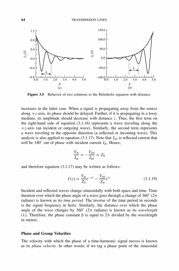
64 TRANSMISSION LINES
Z0.0 1.0 2.0 3.0 4.0 5.0
−0.8
−0.4
0.0
0.4
0.8
1.2
f 1 (Z
)
f 2 (Z
)
Z
0.0 5.04.03.02.01.0
0.0
50.0
−50.0
100.0
−100.0
150.0
(a) (b)
λλ
Figure 3.5 Behavior of two solutions to the Helmholtz equation with distance.
increases in the latter case. When a signal is propagating away from the sourcealong +z-axis, its phase should be delayed. Further, if it is propagating in a lossymedium, its amplitude should decrease with distance z. Thus, the first term onthe right-hand side of equation (3.1.16) represents a wave traveling along the+z-axis (an incident or outgoing wave). Similarly, the second term representsa wave traveling in the opposite direction (a reflected or incoming wave). Thisanalysis is also applied to equation (3.1.17). Note that Iref is reflected current thatwill be 180 out of phase with incident current Iin. Hence,
Vin
Iin= −Vref
Iref= Z0
and therefore equation (3.1.17) may be written as follows:
I (z) = Vin
Z0e−γz − Vref
Z0eγz (3.1.19)
Incident and reflected waves change sinusoidally with both space and time. Timeduration over which the phase angle of a wave goes through a change of 360 (2π
radians) is known as its time period. The inverse of the time period in secondsis the signal frequency in hertz. Similarly, the distance over which the phaseangle of the wave changes by 360 (2π radians) is known as its wavelength(λ). Therefore, the phase constant β is equal to 2π divided by the wavelengthin meters.
Phase and Group Velocities
The velocity with which the phase of a time-harmonic signal moves is knownas its phase velocity. In other words, if we tag a phase point of the sinusoidal

DISTRIBUTED CIRCUIT ANALYSIS OF TRANSMISSION LINES 65
wave and monitor its velocity, we obtain the phase velocity, vp, of this wave.Mathematically,
vp = ω
β
A transmission line has no dispersion if the phase velocity of a propagatingsignal is independent of frequency. Hence, a graphical plot of ω versus β willbe a straight line passing through the origin. This type of plot is called thedispersion diagram of a transmission line. An information-carrying signal iscomposed of many sinusoidal waves. If the line is dispersive, each of theseharmonics will travel at a different velocity. Therefore, the information will bedistorted at the receiving end. The velocity with which a group of waves travelsis called the group velocity, vg. It is equal to the slope of the dispersion curve ofthe transmission line.
Consider two sinusoidal signals with angular frequencies ω + δω and ω − δω,respectively. Assume that these waves of equal amplitudes are propagating in thez-direction with corresponding phase constants β + δβ and β − δβ. The resultingwave can be found as follows:
f (z, t) = Re[Aej [(ω+δω)t−(β+δβ)z] + Aej [(ω−δω)t−(β−δβ)z]]
= 2A cos(δωt − δβz) cos(ωt − βz)
Hence, the resulting wave, f (z, t), is amplitude modulated. The envelope of thissignal moves with the group velocity,
vg = δω
δβ
Example 3.2 A signal generator has an internal resistance of 50 and an open-circuit voltage v(t) = 3 cos(2π × 108t) V. It is connected to a 75- losslesstransmission line that is 4 m long and terminated by a matched load at the otherend. If the signal propagation velocity on this line is 2.5 × 10⁸ m/s, find theinstantaneous voltage and current at an arbitrary location on the line.
SOLUTION Since the transmission line is terminated by a load that is equal toits characteristic impedance, there will be no echo signal. Further, an equivalentcircuit at its input end may be drawn as shown in Figure 3.6. Using the voltage-division rule and Ohm’s law, incident voltage and current can be determinedas follows:
incident voltage at the input end, Vin(z = 0) = 75
50 + 753 0 = 1.8 0 V
incident current at the input end, Iin(z = 0) = 3 0
50 + 75= 0.024 0 A

66 TRANSMISSION LINES
3V∠0°3V∠0°
50 Ω 4 m
75 Ω75 Ω75 Ω
50 Ω
z
Figure 3.6 Circuit arrangement for Example 3.2.
and
β = ω
vp
= 2π × 108
2.5 × 108= 0.8π rad/m
Therefore, V (z) = 1.8e−j0.8πz V and I (z) = 0.024e−j0.8πz A. Hence,
v(z, t) = 1.8 cos(2π × 108t − 0.8πz) V and
i(z, t) = 0.024 cos(2π × 108t − 0.8πz) A
Example 3.3 The parameters of a transmission line are R = 2 /m, G = 0.5mS/m, L = 8 nH/m, and C = 0.23 pF/m. If the signal frequency is 1 GHz, cal-culate its characteristic impedance (Z0) and the propagation constant (γ).
SOLUTION
Z0 =√
R + jωL
G + jωC=
√2 + j2π × 109 × 8 × 10−9
0.5 × 10⁻³ + j2π × 109 × 0.23 × 10−12
=√
2 + j50.2655
0.5 × 10⁻³ + j1.4451 × 10−3 =
√50.31 1.531 rad
15.29 × 10⁻⁴ 1.2377 rad
= 181.39 8.4 = 179.44 + j26.51
and
γ = √ZY =
√(50.31 1.531 rad) × (15.29 × 10⁻⁴ 1.2377 rad)
= 0.2774 79.31m−1 = 0.0514 + j0.2726 m−1 = α + jβ
Therefore, α = 0.0514 Np/m and β = 0.2726 rad/m.
Example 3.4 Two antennas are connected through a quarter-wavelength-longlossless transmission line, as shown in Figure 3.7. However, the characteristic

SENDING-END IMPEDANCE 67
(λ/4)
A
B
jX
80 + j35 Ω
56 + j28 Ω
50 ΩZ0 = ?
z
Figure 3.7 Circuit arrangement for Example 3.4.
impedance of this line is unknown. The array is excited through a 50- line.Antenna A has an impedance of 80 + j35 and antenna B has 56 + j28 . Cur-rents (peak values) through these antennas are found to be 1.5 0 and 1.5 90 A,respectively. Determine the characteristic impedance of the line connecting thesetwo antennas and the value of a reactance connected in series with antenna B.
SOLUTION Assume that Vin and Vref are the incident and reflected phasor volt-ages, respectively, at antenna A. Therefore, the current, IA, through this antenna is
IA = Vin − Vref
Z0= 1.5 0 A ⇒ Vin − Vref = Z0IA = Z01.5 0V
Since the connecting transmission line is a quarter-wavelength long, the incidentand reflected voltages across the transmission line at the location of B will be jVin
and −jVref, respectively. Therefore, the total voltage, VTBX, appearing across theantenna B and the reactance jX combined will be equal to j (Vin − Vref).
VTBX = j (Vin − Vref) = jZ0IA = j1.5Z0 = 1.5Z0 90
Also, Ohm’s law can be used to find this voltage as follows:
VTBX = (56 + j28 + jX)1.5 90
Therefore, X = −28 and Z0 = 56 . Note that the unknown characteristicimpedance is a real quantity because the transmission line is lossless.
3.2 SENDING-END IMPEDANCE
Consider a transmission line of length l and characteristic impedance Z0. It isterminated by a load impedance ZL, as shown in Figure 3.8. Assume that the

68 TRANSMISSION LINES
Z0
LoadZL
z = 0 z = l
Iin
Iref
V in + VrefZin
Figure 3.8 Transmission line terminated by a load impedance.
incident and reflected voltages at its input (z = 0) are Vin and Vref, respectively.The corresponding currents are represented by Iin and Iref.
If V (z) represents the total phasor voltage at point z on the line and I (z) isthe total current at that point,
V (z) = Vine−γz + Vrefe
γz (3.2.1)
and
I (z) = Iine−γz + Irefe
γz (3.2.2)
where Vin, Vref, Iin, and Iref are incident voltage, reflected voltage, incident cur-rent, and reflected current at z = 0, respectively.
Impedance at the input of this transmission line, Zin, can be found after dividingtotal voltage by the total current at z = 0. Thus,
Zin = V (z = 0)
I (z = 0)= Vin + Vref
Iin + Iref= Vin + Vref
Vin/Z0 − Vref/Z0= Z0
Vin + Vref
Vin − Vref
or
Zin = Z01 + Vref/Vin
1 − Vref/Vin= Z0
1 + 0
1 − 0(3.2.3)
where 0 = ρejφ is known as the input reflection coefficient. Further,
Zin = Z01 + 0
1 − 0⇒ Zin
Z0= Zin = 1 + 0
1 − 0
where Zin is called the normalized input impedance. Similarly, voltage and currentat z = l are related through load impedance as follows:
ZL = V (z = l)
I (z = l)= Vine
−γl + Vrefe+γl
Iine−γl + Irefe
+γl
= Z0Vine
−γl + Vrefe+γl
Vine−γl − Vrefe+γl= Z0
e−γl + 0e+γl
e−γl − 0e+γl

SENDING-END IMPEDANCE 69
Therefore,
ZL = e−γl + 0eγl
e−γl − 0e+γl⇒ 0 = ZL − 1
ZL + 1e−2γl (3.2.4)
and equation (3.2.3) can be written as follows:
Zin = 1 + [(ZL − 1)/(ZL + 1)]e−2γl
1 − [(ZL − 1)/(ZL + 1)]e−2γl= ZL(1 + e−2γl) + (1 − e−2γl)
ZL(1 − e−2γl) + (1 + e−2γl)
since
1 − e−2γl
1 + e−2γl= e+γl − e−γl
e+γl + e−γl= sinh γl
cosh γl= tanh γl
Zin = ZL + tanh γl
1 + ZL tanh γl
or
Zin = Z0ZL + Z0 tanh γl
Z0 + ZL tanh γl(3.2.5)
For a lossless line, γ = α + jβ = jβ, and therefore tanh γl = tanh jβl = j tan βl.Hence, equation (3.2.5) simplifies as follows:
Zin = Z0ZL + jZ0 tan βl
Z0 + jZL tan βl(3.2.6)
It is to be noted from this equation that Zin repeats periodically every one-halfwavelength on the transmission line. In other words, the input impedance on alossless transmission line will be the same at points d ± nλ/2, where n is aninteger, due to the fact that
βl = 2π
λ
(d ± nλ
2
)= 2πd
λ± nπ
and
tan βl = tan
(2πd
λ± nπ
)= tan
2πd
λ
Some special cases are as follows:
1. ZL = 0 (i.e., a lossless line is short circuited) ⇒ Zin = jZ0 tan βl.
2. ZL = ∞ (i.e., a lossless line has an open circuit at the load) ⇒ Zin =−jZ0 cot βl.
3. l = λ/4, and therefore βl = π/2 ⇒ Zin = Z20/ZL.

70 TRANSMISSION LINES
According to the first two cases, a lossless line can be used to synthesize anarbitrary reactance. The third case indicates that a quarter-wavelength-long lineof suitable characteristic impedance can be used to transform a load impedanceZL to a new value of Zin. This type of transmission line, called an impedancetransformer , is useful in impedance-matching applications. Further, this equationcan be rearranged as follows:
Zin = 1
ZL
= YL
Hence, normalized impedance at a point a quarter-wavelength away from theload is equal to the normalized load admittance.
Example 3.5 A transmission line of length d and characteristic impedance Z0
acts as an impedance transformer to match a 150- load to a 300- line (seeFigure 3.9). If the signal wavelength is 1 m, find (a) d , (b) Z0, and (c) the reflec-tion coefficient at the load.
SOLUTION(a) d = λ/4 → d = 0.25 m(b) Z0 = √
ZinZL → Z0 = (150 × 300)1/2 = 212.132
(c) L = ZL − 1
ZL + 1= ZL − Z0
ZL + Z0= 150 − 212.132
150 + 212.132= 0.1716
Example 3.6 Design a quarter-wavelength transformer to match a 20- load tothe 45- line at 3 GHz. If this transformer is made from a Teflon-filled (εr = 2.1)coaxial line, calculate its length (in centimeters). Also, determine the diameter ofits inner conductor if the inner diameter of the outer conductor is 0.5 cm. Assumethat the impedance transformer is lossless.
SOLUTION
Z0 = √ZinZL = √
45 × 20 = 30
and
Z0 =√
L
C=
√200 × 10−9
55.63 × εr × 10−12ln
b
a= 30
300 Ω
150 ΩZ0
d
Figure 3.9 Circuit arrangement for Example 3.5.

SENDING-END IMPEDANCE 71
Therefore,
lnb
a= 30
41.3762= 0.7251
andb
a= 2b
2a= e0.7251 = 2.0649 ⇒ 2a = 2b
2.0649= 0.5
2.0649= 0.2421 cm
Phase constant β = ω√
LC:
β = 2π
λ⇒ 1
λ= ω
2π
√LC = f ×
√200 × 55.63 × εr × 10−21
= 3 × 109 × 10−10 × √200 × 55.63 × 2.1 × 0.1
= 14.5011 m−1
Therefore, λ = 0.06896 m and d = λ/4 = 0.01724 m = 1.724 cm.
Example 3.7 Design a quarter-wavelength microstrip impedance transformer tomatch a patch antenna of 80 with a 50- line. The system is to be fabricatedon a 1.6-mm-thick substrate (εr = 2.3) that operates at 2 GHz (see Figure 3.10).
SOLUTION The characteristic impedance of the microstrip line impedancetransformer must be
Z0 = √Z01ZL = 63.2456
Design formulas for microstrip line are given in Appendix 2. Assume that thestrip thickness t is less than 0.096 mm and that the dispersion is negligible forthe time being at the operating frequency.
A = 63.2456
60
(2.3 + 1
2
)1/2
+ 2.3 − 1
2.3 + 1×
(0.23 + 0.11
2.3
)= 1.4635
B = 60π2
63.2456√
2.3= 6.1739
d
ZLZ0Z01
Figure 3.10 Circuit arrangement for Example 3.7.

72 TRANSMISSION LINES
Since A ≤ 1.52,
w
h= 2
π
6.1739 − 1 − ln(2 × 6.1739 − 1)
+2.3 − 1
2 × 2.3
[ln(6.1739 − 1) + 0.39 − 0.61
2.3
]
= 2 × 3.2446
π= 2.0656 ⇒ w = 3.3 mm
At this point, we can check if the dispersion in the line is really negligible. Forthat, we determine the effective dielectric constant as follows:
F(w
h
)=
(1 + 12
h
w
)−1/2
=(
1 + 12
2.0656
)−1/2
= 0.383216
Assuming that t/h = 0.005,
εe = 2.3 + 1
2+ 2.3 − 1
2× 0.383216 − 2.3 − 1
4.6× 0.005√
2.0656= 1.8981 ≈ 1.9
and
F = 4h√
εr − 1
λ0
0.5 +
[1 + 2 × log
(1 + w
h
)]2
= 0.213712
εe(f ) =( √
2.3 − √1.9
1 + 4 × F −1.5+ √
1.9
)2
= 1.909192
Since εe(f ) is very close to εe, dispersion in the line can be neglected. Therefore,
λ = 3 × 10⁸
2 × 10⁹ × √1.9
m = 10.8821 cm ⇒ length of line = 10.8821
4= 2.72 cm
Reflection Coefficient, Return Loss, and Insertion Loss
The voltage reflection coefficient is defined as the ratio of reflected to inci-dent phasor voltages at a location in the circuit. In the case of a transmis-sion line terminated by load ZL, the voltage reflection coefficient is given byequation (3.2.4). Hence,
= Vref
Vin= ZL − Z0
ZL + Z0e−2γl = ρLejθe−2(α+jβ)l = ρLe−2αle−j (2βl−θ) (3.2.7)

SENDING-END IMPEDANCE 73
Real part
−1.0 −0.5 0.0 0.5 1.0
Imag
. par
t
−1.0
−0.5
0.0
0.5
1.0
(a)Real part
−1.0 −0.5 0.0 0.5 1.0
Imag
. par
t
−1.0
−0.5
0.0
0.5
1.0
(b)
Figure 3.11 Reflection coefficient on (a) a lossy and (b) a lossless transmission line.
where ρLejθ = (ZL − Z0)/(ZL + Z0) is called the load reflection coefficient .Equation (3.2.7) indicates that the magnitude of reflection coefficient decreasesby a factor of e−2αl as the observation point moves away from the load. Further,its phase angle changes by −2βl. A polar (magnitude and phase) plot of it willlook like a spiral, as shown in Figure 3.11(a). However, the magnitude of reflec-tion coefficient will not change if the line is lossless. Therefore, the reflectioncoefficient point will be moving clockwise on a circle of radius equal to its mag-nitude as the line length is increased. As illustrated in Figure 3.11 (b), it makesone complete revolution for each half-wavelength distance away from the load(because −2βλ/2 = −2π).
Similarly, the current reflection coefficient, c, is defined as a ratio of reflectedto incident signal-current phasors. It is related to the voltage reflection coefficientas follows:
c = Iref
Iin= −Vref/Z0
Vin/Z0= −
The return loss of a device is defined as the ratio of reflected power to incidentpower at its input. Since the power is proportional to the square of the voltageat that point, it may be found as
return loss = reflected power
incident power= ρ2
Generally, it is expressed in decibels as follows:
return loss = 20 log10 ρ dB (3.2.8)
The insertion loss of a device is defined as the ratio of power transmitted(power available at the output port) to that of the power incident at its input.Since the power transmitted is equal to the difference of the incident and reflected
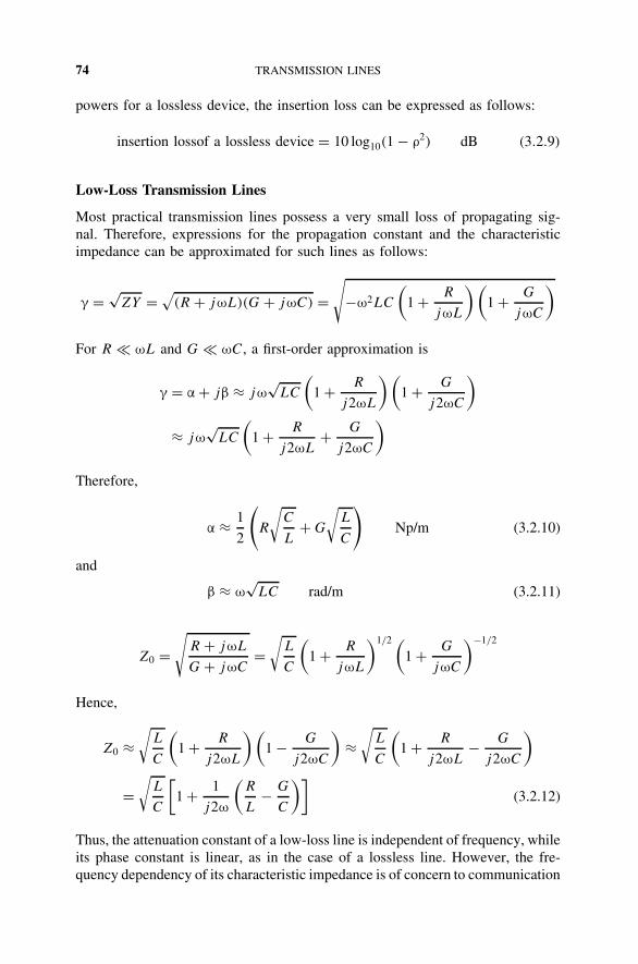
74 TRANSMISSION LINES
powers for a lossless device, the insertion loss can be expressed as follows:
insertion lossof a lossless device = 10 log10(1 − ρ2) dB (3.2.9)
Low-Loss Transmission Lines
Most practical transmission lines possess a very small loss of propagating sig-nal. Therefore, expressions for the propagation constant and the characteristicimpedance can be approximated for such lines as follows:
γ = √ZY = √
(R + jωL)(G + jωC) =√
−ω2LC
(1 + R
jωL
) (1 + G
jωC
)
For R ωL and G ωC, a first-order approximation is
γ = α + jβ ≈ jω√
LC
(1 + R
j2ωL
)(1 + G
j2ωC
)
≈ jω√
LC
(1 + R
j2ωL+ G
j2ωC
)
Therefore,
α ≈ 1
2
(R
√C
L+ G
√L
C
)Np/m (3.2.10)
and
β ≈ ω√
LC rad/m (3.2.11)
Z0 =√
R + jωL
G + jωC=
√L
C
(1 + R
jωL
)1/2 (1 + G
jωC
)−1/2
Hence,
Z0 ≈√
L
C
(1 + R
j2ωL
)(1 − G
j2ωC
)≈
√L
C
(1 + R
j2ωL− G
j2ωC
)
=√
L
C
[1 + 1
j2ω
(R
L− G
C
)](3.2.12)
Thus, the attenuation constant of a low-loss line is independent of frequency, whileits phase constant is linear, as in the case of a lossless line. However, the fre-quency dependency of its characteristic impedance is of concern to communication

SENDING-END IMPEDANCE 75
engineers, because it will distort the signal. If RC = GL, the frequency-dependentterm will go to zero. This type of low-loss line is called a distortionless line. Hence,
γ = √ZY = √
(R + jωL)(G + jωC)
= (R + jωL)
√C
L= α + jβ
(∵G = RC
L
)(3.2.13)
Example 3.8 A signal propagating through a 50- distortionless transmissionline attenuates at the rate of 0.01 dB/m. If this line has a capacitance of 100 pF/m,find (a) R, (b) L, (c) G, and (d) vp.
SOLUTION Since the line is distortionless,
Z0 =√
L
C= 50
andα = 0.01 dB/m ≈ 0.01/8.69 Np/m = 1.15 × 10⁻³ Np/m
Hence,
(a) R = α√
L/C = 1.15 × 10−3 × 50 = 0.057 / m(b) L = CZ2
0 = 10−10 × 502 H/m = 0.25 µH/m(c) G = RC/L = R/Z2
0 = 0.057/502 S/m = 22.8µS/ m
(d) vp = 1/√
LC = 2 × 10⁸ m/s
Experimental Determination of Characteristic Impedance and PropagationConstant of a Transmission Line
A transmission line of length d is kept open at one end, and the impedance atits other end is measured using an impedance bridge. Assume that it is Zoc. Theprocess is repeated after placing a short circuit at its open end, and this impedanceis recorded as Zsc. Using equation (3.2.5), one can write
Zoc = Z0 coth γd (3.2.14)
and
Zsc = Z0 tanh γd (3.2.15)
Therefore,Z0 = √
ZocZsc (3.2.16)
and
tanh γd =√
Zsc
Zoc⇒ γ = 1
dtanh−1
√Zsc
Zoc(3.2.17)

76 TRANSMISSION LINES
These two equations can be solved to determine Z0 and γ. The following identitycan be used to facilitate the evaluation of the propagation constant:
tanh−1 Z = 1
2ln
1 + Z
1 − Z
The following examples illustrate this procedure.
Example 3.9 Impedance at one end of the transmission line is measured to beZin = 30 + j60 using an impedance bridge, while its other end is terminatedby a load ZL. The experiment is repeated twice, with the load replaced first bya short circuit and then by an open circuit. These data are recorded as j53.1
and −j48.3 , respectively. Find the characteristic resistance of this line and theload impedance.
SOLUTION
Z0 = √Zsc × Zoc = √
j53.1 × (−j48.3) = 50.6432
Zin = Z0ZL + jZ0 tan βl
Z0 + jZL tan βl= Z0
ZL + Zsc
Z0 + jZL tan βl
= Z0
j tan βl
ZL + Zsc
ZL + Z0/(j tan βl)
Therefore,
Zin = ZocZL + Zsc
ZL + Zoc⇒ ZL = Zoc
Zsc − Zin
Zin − Zoc
ZL = −j48.3 × j53.1 − (30 + j60)
30 + j60 − (−j48.3)
Therefore,ZL = 11.6343 + j6.3
Example 3.10 Measurements are made on a 1.5-m-long transmission line usingan impedance bridge. After short-circuiting at one of its ends, impedance at theother end is found to be j103 . Repeating the experiment with the short circuitnow replaced by an open circuit gives −j54.6 . Determine the propagationconstant and the characteristic impedance of this line.
SOLUTION
Z0 = √ZocZsc = √−j54.6 × j103 = 74.99 ≈ 75
tanh 1.5γ =√
j103
−j54.3= j1.8969 ⇒ 1.5γ = tanh−1 j1.8969

SENDING-END IMPEDANCE 77
= 1
2ln
1 + j1.8969
1 − j1.8969
1.5γ = 1
2ln
1 + j1.8969
1 − j1.8969= 1
2ln(1 2.1713 rad)= 1
2ln(ej2.1713)=j1.08565
and γ = j0.7238 m−1.
Example 3.11 A 10-m-long 50- lossless transmission line is terminated bya load, ZL = 100 + j50 . It is driven by a signal generator that has an open-circuit voltage Vs at 100 0 V and source impedance Zs at 50 . The propagatingsignal has a phase velocity of 200 m/µS at 26 MHz. Determine the impedance atits input end and the phasor voltages at both its ends (see Figure 3.12).
SOLUTION
Zin = Z0ZL + jZ0 tan βl
Z0 + jZL tan βland β = ω
vp
= 2π × 26 × 106
200 × 106= 0.8168 rad/m
= 50100 + j50 + j50 tan(8.168)
50 + j (100 + j50) tan(8.168)= 19.5278 0.181 rad
= 19.21 + j3.52
The equivalent circuits at its input and at the load can be drawn as in Figure 3.13.
Voltage at the input end, VA = Vs
Zs + ZinZin = 100 × 19.5278 0.181 rad
50 + 19.21 + j3.52V
ZL
Zs
10 m
Vs
Figure 3.12 Circuit arrangement for Example 3.11.
Zin
Zs
VsZL
ZTh
VTh
VA
Figure 3.13 Equivalent circuits at the two ends of the transmission line shown inFigure 3.12.

78 TRANSMISSION LINES
or
VA = 1952.78 0.181 rad
69.2995 0.0508 rad= 28.1788 V 0.1302 rad = 28.1788 V 7.46
For determining voltage at the load, a Thevenin equivalent circuit can be usedas follows:
ZTh = Z0Zs + jZ0 tan βl
Z0 + jZs tan βl= Z0 (∵Zs = Z0 = 50 )
and
VTh = (Vin + Vref)at o.c. = (2 × Vin)at o.c. = 100 V −8.168 rad
Therefore,
VL = VTh
ZTh + ZL
ZL = 100 −8.168 rad
50 + 100 + j50× (100 + j50) V
or
VL = 70.71 V −8.0261 rad = 70.71 V −459.86 = 70.71 V −99.86
Alternatively,
V (z) = Vine−jβz + Vrefe
jβz = Vin(e−jβz + ejβz)
where Vin is incident voltage at z = 0 and is the input reflection coefficient.
Vin = 50 V 0
and
= 19.21 + j3.52 − 50
19.21 + j3.52 + 50= 0.4472 2.9769 rad
Hence,
VL = V (z = 10 m) = 50(e−j8.168 + 0.4472ej(2.9769+8.168))
= 50 × 1.4142 V −1.743 rad
or
VL = 70.7117 V −99.8664
Example 3.12 Two identical signal generators are connected in parallel througha quarter-wavelength-long lossless 50- transmission line (Figure 3.14). Each ofthese generators has an open-circuit voltage of 12 0 V and a source impedance

SENDING-END IMPEDANCE 79
λ/4 λ/4
10 Ω50 Ω50 Ω
Z0 = 50 ΩZ0 = 50 Ω
12 V∠0° 12 V∠0°A B
Figure 3.14 Circuit arrangement for Example 3.12.
of 50 . It drives a 10- load through another quarter-wavelength-long similartransmission line. Determine the power dissipated by the load.
SOLUTION The signal generator connected at the left (source A) and thequarter-wavelength-long line connecting it can be replaced by a Thevenin equiv-alent voltage source of 12 V −90 with its internal resistance at 50 . Thisvoltage source can be combined with the 12 0 V (source B) already there,which also has an internal resistance of 50 . The resulting source will havea Thevenin voltage of 6 − j6 V = 6
√2 V −45 and an internal resistance of
25 (i.e., two 50- resistances connected in parallel). The load will transformto 50 × 50/10 = 250 at the location of source B. Therefore, a simplified circuitcan be drawn as in Figure 3.15.
The voltage across 250 will be equal to
250 × 6 − j6
275 V= 60
√2/11 −45V
Thus, the dissipated power, Pd , can be calculated as follows:
Pd = 602 × 2
112 × 2 × 250= 0.119008 W = 119.008 mW
250 Ω
25 Ω
6√2 V∠−45°
Figure 3.15 Simplification of the circuit shown in Figure 3.14.

80 TRANSMISSION LINES
3.3 STANDING WAVE AND STANDING WAVE RATIO
Consider a lossless transmission line that is terminated by a load impedance ZL,as shown in Figure 3.16. Incident and reflected voltage phasors at its input (i.e.,at z = 0) are assumed to be Vin and Vref, respectively. Therefore, total voltageV (z) can be expressed as follows:
V (z) = Vine−jβz + Vrefe
+jβz
Alternatively, V (x) can be written as
V (x) = V+e+jβx + V−e−jβx = V+(e+jβx + e−jβx)
orV (x) = V+[e+jβx + ρe−j (βx−φ)] (3.3.1)
where
= ρejφ = V−V+
V+ and V− represent incident and reflected wave voltage phasors, respectively,at the load point (i.e., at x = 0).
Let us first consider two extreme conditions at the load. In one case, thetransmission line has an open circuit, whereas in the other, it has a short-circuittermination. Therefore, the magnitude of the reflection coefficient, ρ, is unity inboth cases. However, the phase angle, φ, is zero for the former case and π forthe latter. Phasor diagrams for these two cases are depicted in Figure 3.17(a)and (b), respectively. As distance x from the load increases, the phasor ejβx
rotates counterclockwise because of the increase in its phase angle βx. On theother hand, the phasor e−jβx rotates clockwise by the same amount. Therefore, thephase angle of the resulting voltage, V (x), remains constant with space coordinatex while its magnitude varies sinusoidally between ±2V+. Since the phase angleof the resulting signal V (x) does not change with distance, it does not represent
Vin
Vref
V+
V−
xz
Figure 3.16 Lossless transmission line with termination.

STANDING WAVE AND STANDING WAVE RATIO 81
(a) (b)
e jβx
e−jβx
V(x)
βx
−βx
βx
π − βx
V(x)
e jβx
e−j(βx − π)
Figure 3.17 Phasor diagrams of line voltage with (a) open-circuit and (b) short-circuittermination.
a propagating wave. Note that there are two waves propagating on this line inopposite directions. However, the resulting signal represents a standing wave.
When the terminating load is of an arbitrary value that is different from thecharacteristic impedance of the line, there are still two waves propagating inopposite directions. The interference pattern of these two signals is stationarywith time. Assuming that V+ is unity, a phasor diagram for this case is drawnas shown in Figure 3.18. The magnitude of the resulting signal, V (x), can bedetermined using the law of parallelograms as follows:
|V (x)| = |V+|[1 + ρ2 + 2ρ cos(2βx − φ)]1/2 (3.3.2)
θ
βx
−(βx − φ)
(2βx − φ)
V(x)
ejβx
ρe−j(βx − φ)
Figure 3.18 Phasor diagram of line voltage with arbitrary termination.

82 TRANSMISSION LINES
The reflection coefficient, (x), can be expressed as
(x) = V−e−jβx
V+ejβx= ρe−j (2βx−φ) (3.3.3)
Hence, the magnitude of this standing wave changes with location on thetransmission line. Since x appears only in the argument of cosine function, thevoltage magnitude has an extreme value whenever this argument is an integermultiple of π. It has a maximum whenever the reflected wave is in phase withthe incident signal, which requires that the following condition be satisfied:
2βx − φ = ±2nπ, n = 0, 1, 2, . . . (3.3.4)
On the other hand, V (x) has a minimum value where the reflected and incidentsignals are out of phase. Hence, x satisfies the following condition at a minimumof the interference pattern:
2βx − φ = ±(2m + 1)π, m = 0, 1, 2, . . . (3.3.5)
Further, these extreme values of the standing waves are
|V (x)|max = |V+|(1 + ρ) (3.3.6)
and
|V (x)|min = |V+|(1 − ρ) (3.3.7)
The ratio of maximum to minimum values of voltage V (x) is called the voltagestanding wave ratio (VSWR). Therefore,
VSWR = S = |V (x)|max
|V (x)|min= 1 + ρ
1 − ρ(3.3.8)
Since 0 ≤ ρ ≤ 1 for a passive load, the minimum value of the VSWR will beunity (for a matched load) while its maximum value can be infinity (for totalreflection, with a short circuit or an open circuit as the load).
Assume that there is a voltage minimum at x1 from the load, and if one keepsmoving toward the source, the next minimum occurs at x2. In other words, thereare two consecutive minimums at x1 and x2 with x2 > x1. Hence,
2(βx1 − φ) = (2m1 + 1)π
and
2(βx2 − φ) = [2(m1 + 1) + 1]π
Subtracting the former equation from the latter, one finds that
2β(x2 − x1) = 2π ⇒ x2 − x1 = λ
2
where x2 − x1 is the separation between the two consecutive minimums.
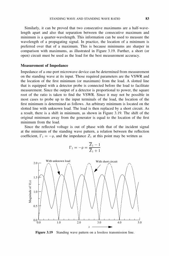
STANDING WAVE AND STANDING WAVE RATIO 83
Similarly, it can be proved that two consecutive maximums are a half-wave-length apart and also that separation between the consecutive maximum andminimum is a quarter-wavelength. This information can be used to measure thewavelength of a propagating signal. In practice, the location of a minimum ispreferred over that of a maximum. This is because minimums are sharper incomparison with maximums, as illustrated in Figure 3.19. Further, a short (oropen) circuit must be used as the load for the best measurement accuracy.
Measurement of Impedance
Impedance of a one-port microwave device can be determined from measurementon the standing wave at its input. Those required parameters are the VSWR andthe location of the first minimum (or maximum) from the load. A slotted linethat is equipped with a detector probe is connected before the load to facilitatemeasurement. Since the output of a detector is proportional to power, the squareroot of the ratio is taken to find the VSWR. Since it may not be possible inmost cases to probe up to the input terminals of the load, the location of thefirst minimum is determined as follows. An arbitrary minimum is located on theslotted line with unknown load. The load is then replaced by a short circuit. Asa result, there is a shift in minimum, as shown in Figure 3.19. The shift of theoriginal minimum away from the generator is equal to the location of the firstminimum from the load.
Since the reflected voltage is out of phase with that of the incident signalat the minimum of the standing wave pattern, a relation between the reflectioncoefficient, 1 = −ρ, and the impedance Z1 at this point may be written as
1 = −ρ = Z1 − 1
Z1 + 1
With short circuit
x
0.0 1.0 2.0 3.0 4.0 5.00.0
0.5
1.0
1.5
2.0
Mag
nitu
de o
f V
(x)
With unknown load
Figure 3.19 Standing wave pattern on a lossless transmission line.

84 TRANSMISSION LINES
where Z1 is the normalized impedance at the location of the first minimum ofthe voltage standing wave. Since
S = 1 + ρ
1 − ρand ρ = S − 1
S + 1
and therefore,
−S − 1
S + 1= Z1 − 1
Z1 + 1⇒ Z1 = 1
S
This normalized impedance is equal to the input impedance of a line that isterminated by load ZL and has a length of d1. Hence,
Z1 = 1
S= ZL + j tan βd1
1 + jZL tan βd1⇒ ZL = 1 − jS tan βd1
S − j tan βd1
Similarly, the reflected voltage is in phase with the incident signal at themaximum of the standing wave. Assume that the first maximum is located at adistance d2 from the unknown load and that the impedance at this point is Z2.One can write
2 = ρ = Z2 − 1
Z2 + 1= S − 1
S + 1⇒ Z2 = S
and
ZL = Z2 − j tan βd2
1 − jZ2 tan βd2
Since the maximum and minimum are measured on a lossless line that feedsthe unknown load, magnitude of the reflection coefficient ρ does not change atdifferent points on the line.
Example 3.13 A load impedance of 73 − j42.5 terminates a transmissionline of characteristic impedance 50 + j0.01 . Determine its reflection coefficientand the voltage standing wave ratio.
SOLUTION
= ZL − Z0
ZL + Z0= 73 − j42.5 − (50 + j0.01)
73 − j42.5 + (50 + j0.01)
= 23 − j42.51
123 − j42.49= 48.3332 −1.0749 rad
130.1322 −0.3326 rad
= 0.3714 −0.7423 rad = 0.3714 −42.53
and
VSWR = 1 + ρ
1 − ρ= 1 + 0.3714
1 − 0.3714= 2.1817

SMITH CHART 85
Note that this line is lossy, and therefore the reflection coefficient and VSWRwill change with distance from the load.
Example 3.14 A 100- transmission line is terminated by the load ZL. Mea-surements indicate that it has a VSWR of 2.4 and the standing wave minimumsare 100 cm apart. The scale reading at one of these minimums is found to be275 cm. When the load is replaced by a short circuit, the minimum moves awayfrom the generator to a point where the scale shows 235 cm. Find the signalwavelength and the load impedance.
SOLUTION Since the minimums are 100 cm apart, the signal wavelength λ =2 × 100 = 200 cm = 2 m, β = π rad/m, and d1 = 275 − 235 = 40 cm. Hence,
ZL = 1 − j2.4 tan(0.4π)
2.4 − j tan(0.4π)= 1.65 − j0.9618
or
ZL = 165 − j96.18
3.4 SMITH CHART
Normalized impedance at a point in the circuit is related to its reflection coeffi-cient as
Z = R + jX = 1 +
1 − = 1 + r + ji
1 − r − ji
(3.4.1)
where r and i represent real and imaginary parts of the reflection coeffi-cient, while R and X are real and imaginary parts of the normalized impedance,respectively. This complex equation can be split into two, after equating real andimaginary components on its two sides. Hence,(
r − R
1 + R
)2
+ 2i =
(1
1 + R
)2
(3.4.2)
and
(r − 1)2 +(
i − 1
X
)2
=(
1
X
)2
(3.4.3)
These two equations represent a family of circles on the complex -plane. Thecircle in (3.4.2) has its center at (R/(1 + R), 0) and a radius of 1/(1 + R). ForR = 0 it is centered at the origin with unity radius. As R increases, the centerof the constant-resistance circle moves on a positive real axis and its radiusdecreases. When R = ∞, the radius reduces to zero and the center of the circlemoves to (1,0). These plots are shown in Figure 3.20. Note that for passiveimpedance, 0 ≤ R ≤ ∞ and −∞ ≤ X ≤ +∞.
Similarly, (3.4.3) represents a circle that is centered at (1, 1/X) with a radiusof 1/X. For X = 0, its center lies at (1,∞) with an infinite radius. Hence, it is a
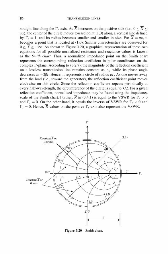
86 TRANSMISSION LINES
straight line along the r -axis. As X increases on the positive side (i.e., 0 ≤ X ≤∞), the center of the circle moves toward point (1,0) along a vertical line definedby r = 1, and its radius becomes smaller and smaller in size. For X = ∞, itbecomes a point that is located at (1,0). Similar characteristics are observed for0 ≥ X ≥ −∞. As shown in Figure 3.20, a graphical representation of these twoequations for all possible normalized resistance and reactance values is knownas the Smith chart. Thus, a normalized impedance point on the Smith chartrepresents the corresponding reflection coefficient in polar coordinates on thecomplex -plane. According to (3.2.7), the magnitude of the reflection coefficienton a lossless transmission line remains constant as ρL while its phase angledecreases as −2βl. Hence, it represents a circle of radius ρL. As one moves awayfrom the load (i.e., toward the generator), the reflection coefficient point movesclockwise on this circle. Since the reflection coefficient repeats periodically atevery half-wavelength, the circumference of the circle is equal to λ/2. For a givenreflection coefficient, normalized impedance may be found using the impedancescale of the Smith chart. Further, R in (3.4.1) is equal to the VSWR for r > 0and i = 0. On the other hand, it equals the inverse of VSWR for r < 0 andi = 0. Hence, R values on the positive r -axis also represent the VSWR.
0 0.1 0.5 1.0 2.0 5.0
0.2
0.5
1.0
2.02.0
0.2
0.51.0
2.02.0
0°
90°
180°
270°
1
Γi
Γr
(1,1)Constant R orG circles
Constant X orB arcs
Figure 3.20 Smith chart.

SMITH CHART 87
Since admittance represents the inverse of impedance, we can write
Y = 1
Z= 1 −
1 +
Hence, a similar analysis can be performed with the normalized admittanceinstead of impedance. It results in the same kind of chart except that the normal-ized conductance circles replace normalized resistance circles, while the normal-ized susceptance arcs replace normalized reactance.
Normalized resistance (or conductance) of each circle is indicated on the r
-axis of the Smith chart. Normalized positive reactance (or susceptance) arcs areshown on the upper half, while negative reactance (or susceptance) arcs are seenin the lower half. The Smith chart in conjunction with equation (3.2.7) facilitatesthe analysis and design of transmission line circuits.
Example 3.15 A load impedance of 50 + j100 terminates a lossless, quarter-wavelength-long transmission line. If characteristic impedance of the line is 50 ,find the impedance at its input end, the load reflection coefficient, and the VSWRon this transmission line.
SOLUTION This problem can be solved using equations (3.2.6), (3.2.7), and(3.3.8) or the Smith chart. Let us try it both ways.
βl = 2π
λ× λ
4= π
2= 90
Zin = Z0ZL + jZ0 tan βl
Z0 + jZL tan βl= 50
(50 + j100) + j50 tan(90)
50 + j (50 + j100) tan(90)or
Zin = 50j50
j (50 + j100)= 2500
50 + j100= 10 − j20
= ZL − Z0
ZL + Z0= 50 + j100 − 50
50 + j100 + 50= j100
100 + j100= 100 90
100 × √2 45
= 0.7071 45
VSWR = 1 + ||1 − || = 1 + 0.7071
1 − 0.7071= 1.7071
0.2929= 5.8283
To solve this problem graphically using the Smith chart, normalized load impe-dance is determined as follows:
ZL = ZL
Z0= 50 + j100
50= 1 + j2
This point is located on the Smith chart as shown in Figure 3.21. A circle thatpasses through 1 + j2 is then drawn with point 1 + j0 as its center. Since the
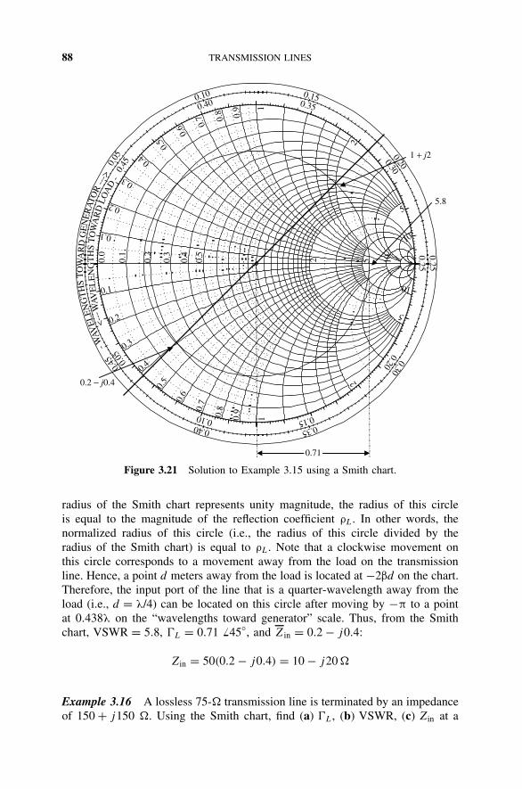
88 TRANSMISSION LINES
0.1
0.3
0.5
0.2
0.4
2 5 10
0.1
0.3
0.5
0.7 0.
9
0.2
0.4
0.6
0.8 1
2
5
10
0.1
0.3
0.5
0.7
0.9
0.2
0.4
0.6
0.8
1
2
5
10
0.05
0.10 0.15
0.20
0.25
0.30
0.350.40
0.45 0.
05
0.10 0.15
0.20
0.25
0.30
0.350.40
0.45
<---
0.0
1 + j2
5.8
0.2 − j0.4
0.71
WA
VE
LE
NG
TH
ST
OW
AR
DLO
AD
--W
AVE
LE
NG
TH
ST
OW
AR
DG
EN
ER
ATO
R--
->
Figure 3.21 Solution to Example 3.15 using a Smith chart.
radius of the Smith chart represents unity magnitude, the radius of this circleis equal to the magnitude of the reflection coefficient ρL. In other words, thenormalized radius of this circle (i.e., the radius of this circle divided by theradius of the Smith chart) is equal to ρL. Note that a clockwise movement onthis circle corresponds to a movement away from the load on the transmissionline. Hence, a point d meters away from the load is located at −2βd on the chart.Therefore, the input port of the line that is a quarter-wavelength away from theload (i.e., d = λ/4) can be located on this circle after moving by −π to a pointat 0.438λ on the “wavelengths toward generator” scale. Thus, from the Smithchart, VSWR = 5.8, L = 0.71 45, and Zin = 0.2 − j0.4:
Zin = 50(0.2 − j0.4) = 10 − j20
Example 3.16 A lossless 75- transmission line is terminated by an impedanceof 150 + j150 . Using the Smith chart, find (a) L, (b) VSWR, (c) Zin at a

SMITH CHART 89
distance of 0.375λ from the load, (d) the shortest length of the line for whichimpedance is purely resistive, and (e) the value of this resistance.
SOLUTION
ZL = 150 + j150
75= 2 + j2
After locating this normalized impedance point on the Smith chart, the constantVSWR circle is drawn as shown in Figure 3.22.
(a) The magnitude of the reflection coefficient is equal to the radius of theVSWR circle (with the radius of the Smith chart as unity). The angle made bythe radial line that connects the load impedance point with the center of the chartis equal to the phase angle of reflection coefficient. Hence,
L = 0.62 30
0.1
0.3
0.5
0.2
0.4
2 5 10
1.0
0.3
0.5
0.7 0.
9
0.2
0.4
0.6
0.8 1
2
5
10
0.1
0.3
0.5
0.7
0.9
0.2
0.4
0.6
0.8
1
2
5
10
0.05
0.10 0.15
0.20
0.25
0.300.350.40
0.45 0.
050.10 0.15
0.20
0.25
0.30
0.350.40
0.45
0.0
2 + j2 0.3 + j 0.54
<---
WA
VE
LE
NG
TH
ST
OW
AR
DLO
AD
--W
AVE
LE
NG
TH
ST
OW
AR
DG
EN
ER
AT
OR
--->
Figure 3.22 Solution to Example 3.16 using a Smith chart.

90 TRANSMISSION LINES
(b) VSWR is found to be 4.25 from the scale reading for the point wherethe circle intersects the +r axis.
(c) For d = 0.375λ, −2βd = −4.7124 rad = −270 (clockwise from theload). This point is located after moving on the VSWR circle by 0.375λ from theload (at 0.084λ on the “wavelengths toward generator” scale). The correspondingnormalized impedance is found to be 0.3 + j0.54. Therefore,
Zin(l = 0.375λ) = 75(0.3 + j0.54) = 22.5 + j40.5
(d) While moving clockwise from the load point, the VSWR circle crossesthe r -axis for the first time at 0.25λ. The imaginary part of impedance is zeroat this intersection point. Therefore, d = (0.25 − 0.208)λ = 0.042λ. Normalizedimpedance at this point is 4.25. The next point on the transmission line wherethe impedance is purely real occurs a quarter-wavelength from it (i.e., 0.292λ
from load). Normalized impedance at this point is 0.23.(e) The normalized resistance and VSWR are the same at this point. Therefore,
R = 75 × 4.25 = 318.75
Example 3.17 A lossless 100- transmission line is terminated by an impedanceof 100 + j100 as illustrated in Figure 3.23. Find the location of the first Vmax,the first Vmin, and the VSWR if the operating wavelength is 5 cm.
SOLUTION
ZL = 100 + j100
100= 1 + j1
As shown in Figure 3.24, this point is located on the Smith chart and the VSWRcircle is drawn. From the chart, VSWR = 2.6. The scale reading on the “wave-lengths toward generator” is 0.162λ at the load point. When one moves awayfrom this point clockwise (toward generator) on this VSWR circle, the voltagemaximum is found first at 0.25λ and then a minimum at 0.5λ. If the first voltagemaximum is at dmax from the load, dmax = (0.25 − 0.162)λ = 0.088λ = 0.44 cm
Zs
Vs
Z0 = 100 Ω ZL = 100 + j100 Ω
Figure 3.23 Circuit arrangement for Example 3.17.

SMITH CHART 91
0.1
0.3
0.5
0.2
0.4
2 5 10
0.1
0.3
0.5
0.7 0.
9
0.2
0.4
0.6
0.8 1
2
5
10
0.1
0.3
0.5
0.7
0.9
0.2
0.4
0.6
0.8
1
2
5
10
0.05
0.10 0.15
0.20
0.25
0.30
0.350.40
0.45 0.
05
0.10 0.15
0.20
0.25
0.300.350.40
0.45
0.0
<---
WA
VE
LE
NG
TH
ST
OW
AR
DLO
AD
-
-WAV
EL
EN
GT
HS
TO
WA
RD
GE
NE
RA
TOR
--->
Figure 3.24 Solution to Example 3.17 using a Smith chart.
from the load. The first minimum is a quarter-wavelength away from the pointof voltage maximum. Hence, dmin = (0.5 − 0.162)λ = 0.338λ = 1.69 cm.
Example 3.18 A 150- load terminates a 75- line. Find the impedance atpoints 2.15λ and 3.75λ from the termination:
ZL = 150
75= 2
SOLUTION As illustrated in Figure 3.25, this point is located on the Smithchart and the VSWR circle is drawn. Note that the VSWR on this line is 2 andthe load reflection coefficient is about 0.33 0. As one moves on the transmis-sion line toward the generator, the phase angle of reflection coefficient changesby −2βd , where d is the distance away from the load. Hence, one revolutionaround the VSWR circle is completed for every half-wavelength. Therefore, the

92 TRANSMISSION LINES
0.1
0.3
0.5
0.2
0.4
2 5 10
0.1
0.3
0.5
0.7 0.
9
0.2
0.4
0.6
0.8 1
2
5
10
0.1
0.3
0.5
0.7
0.9
0.2
0.4
0.6
0.8
1
2
5
10
0.05
0.10 0.15
0.20
0.25
0.30
0.350.40
0.45 0.
05
0.10 0.15
0.20
0.25
0.30
0.350.40
0.45
0.0
-WAV
EL
EN
GT
HS
TO
WA
RD
GE
NE
RA
TO
R--
-><-
---W
AVE
LE
NG
TH
ST
OW
AR
DL
OA
D-
Figure 3.25 Solution to Example 3.18 using a Smith chart.
normalized impedance will be 2 at every integer multiple of a half-wavelengthfrom the load. It will be true for a point located at 2λ as well as at 3.5λ. For theremaining 0.15λ, the impedance point is located on the VSWR circle at 0.40λ
(i.e., 0.25 + 0.15) on the “wavelengths toward generator” scale. Similarly, thepoint corresponding to 3.75λ from the load is found at 0.5λ. From the Smithchart, the normalized impedance at 2.15λ is 0.68 − j0.48, while it is 0.5 at3.75λ. Therefore,
impedance at 2.15λ, Z1 = (0.68 − j0.48) × 75 = 51 − j36
and
impedance at 3.75λ, Z2 = (0.5) × 75 = 37.5 .
Example 3.19 A lossless 100- transmission line is terminated by an admit-tance of 0.0025 − j0.0025 S. Find the impedance at a point 3.15λ away fromthe load and the VSWR on this line.

SMITH CHART 93
SOLUTION
Y L = YL
Y0= YL × Z0 = 0.25 − j0.25
As before, this normalized admittance point is located on the Smith chart andthe VSWR circle is drawn. It is shown in Figure 3.26. There are two choicesavailable at this point. The given normalized load admittance is converted tocorresponding impedance by moving to a point on the diametrically oppositeside of the VSWR circle. It shows a normalized load impedance as 2 + j2.Moving from this point by 3.15λ toward the generator, the normalized impedanceis found as 0.55 − j1.08. Alternatively, we can first move from the normalizedadmittance point by 3.15λ toward the generator to a normalized admittance point0.37 + j0.75. This is then converted to normalized impedance by moving to thediametric opposite point on the VSWR circle. Thus, the normalized impedanceat a point 3.15λ away from the load is 0.55 − j1.08. The impedance at this pointis 100 × (0.55 − j1.08) = 55 − j108 , and the VSWR is approximately 4.3.
0.1
0.3
0.5
0.2
0.4
2 5 10
0.1
0.3
0.5
0.7 0.
9
0.2
0.4
0.6
0.8 1
2
5
10
0.1
0.3
0.5
0.7
0.9
0.2
0.4
0.6
0.8
1
2
5
10
0.05
0.10 0.15
0.20
0.25
0.300.350.40
0.45 0.
05
0.10 0.150.20
0.25
0.30
0.350.40
0.45
0.0
-WAV
EL
EN
GT
HS
TO
WA
RD
GE
NE
RA
TO
R--
-><-
--W
AVE
LE
NG
TH
ST
OW
AR
DL
OA
D-
Figure 3.26 Solution to Example 3.19 using a Smith chart.

94 TRANSMISSION LINES
Example 3.20 An experiment is performed using the circuit illustrated in Figure3.27. First, a load ZL is connected at the end of a 100- transmission line andits VSWR is found to be 2. After that, the detector probe is placed at one ofthe minimums on the line. It is found that this minimum shifts toward the loadby 15 cm when the load is replaced by a short circuit. Further, two consecutiveminimums are found to be 50 cm apart. Determine the load impedance.
Zs
Vs
Z0 = 100 Ω ZL
Figure 3.27 Circuit arrangement for Example 3.20.
0.1
0.3
0.5
0.2
0.4
2 5 10
0.1
0.3
0.5
0.7 0.
9
0.2
0.4
0.6
0.8 1
2
5
10
0.1
0.3
0.5
0.7
0.9
0.2
0.4
0.6
0.8
1
2
5
10
0.05
0.10 0.15
0.20
0.25
0.30
0.350.40
0.45 0.
050.10 0.15
0.20
0.25
0.30
0.350.40
0.45
0.0
-WAV
EL
EN
GT
HS
TO
WA
RD
GE
NE
RA
TO
R--
-><-
--W
AVE
LE
NG
TH
ST
OW
AR
DL
OA
D-
Figure 3.28 Solution to Example 3.20 using a Smith chart.

PROBLEMS 95
SOLUTION Since the separation between consecutive minimums is 50 cm, thesignal wavelength on the line is 100 cm. Therefore, the first minimum of thestanding wave pattern occurs at 0.15λ from the load. Since the VSWR on theline is measured as 2, this circle is drawn on the Smith chart as illustrated inFigure 3.28. As explained in the preceding section, a minimum in a voltagestanding wave occurs when the phase angle of the reflection coefficient is 180.It is located on the Smith chart at a point where the VSWR circle intersects the−r axis. From this point we move toward the load by 0.15λ (i.e., counterclock-wise) to locate the normalized load impedance point. It is found to be 1 −j0.7.Therefore,
ZL = 100 × (1 − j0.7) = 100 − j70
SUGGESTED READING
Collin, R. E., Foundations for Microwave Engineering. New York: McGraw-Hill, 1992.
Edwards, T., Foundations for Microstrip Circuit Design. New York: Wiley, 1992.
Gupta, K. C., and I. J. Bahl, Microstrip Lines and Slotlines. Boston: Artech House, 1979.
Magnusson, P. C., G. C. Alexander, and V. K. Tripathi, Transmission Lines and WavePropagation. Boca Raton, FL: CRC Press, 1992.
Pozar, D. M., Microwave Engineering. New York: Wiley, 1998.
Ramo, S., J. R. Whinnery, and T. Van Duzer. Fields and Waves in Communication Elec-tronics. New York: Wiley, 1994.
Rizzi, P. A., Microwave Engineering. Englewood Cliffs, NJ: Prentice Hall, 1988.
Sinnema, W., Electronic Transmission Technology. Englewood Cliffs, NJ: Prentice Hall,1988.
PROBLEMS
3.1. A lossless semirigid coaxial line has its inner and outer conductor radii as1.325 and 4.16 mm, respectively. Find the line parameters, characteristicimpedance, and the propagation constant for a signal frequency of 500 MHz(εr = 2.1).
3.2. Calculate the magnitude of the characteristic impedance and the propa-gation constant for a coaxial line at 2 GHz. Assume that b = 3 cm, a =0.5 cm, and ε = ε0 (2.56 − j0.005).
3.3. A certain telephone line has the following electrical parameters: R = 40 /mile, L = 1.1 mH/mile, G ≈ 0, and C = 0.062 µF/mile. Loading coils areadded which provide an additional inductance of 30 mH/mile as well as anadditional resistance of 8 /mile. Obtain the attenuation constant and phasevelocities at frequencies of 300 Hz and 3.3 kHz.
3.4. A given transmission line has the following parameters: Z0 = 600 −6,
α = 2.0 × 10⁻⁵ dB/m, vp = 2.97 × 10⁸ m/s, and f = 1.0 kHz. Write phasor

96 TRANSMISSION LINES
V (z) and I (z) and the corresponding instantaneous values for a wave travel-ing in the z-direction if the maximum value of the current wave at z = 0 is0.3 mA and it has a maximum positive value with respect to time at t = 0.
3.5. A 100 + j200- load is connected to a 75- transmission line that is 1 mlong. If signal wavelength on the line is 8 m, find the input impedance andthe signal frequency. Assume that the phase velocity is 70% of the speedof light in free space.
3.6. A 30-km-long transmission line is terminated by a 100 + j200- load. Asinusoidal source with output voltage v(t) = 15 cos(8000πt) V and internalresistance 75 is connected at its other end. The characteristic impedanceof the line is 75 and the phase velocity of the signal is 2.5 × 10⁸ m/s.Find the total voltage across its input end and the load.
3.7. A 2.5-m-long transmission line is short-circuited at one end and the impe-dance at its other end is found to be j5 . When the short is replaced byan open circuit, the impedance at the other end changes to −j500 . A1.9-MHz sinusoidal source is used in this experiment, and the transmissionline is less than a quarter-wavelength long. Determine the characteristicimpedance of the line and phase velocity of the signal.
3.8. A lossless 75- transmission line is connected between the load impedanceof 37.5 − j15 and a signal generator with internal impedance of 75 .Find (a) the reflection coefficient at 0.15λ from the load, (b) the VSWRon the line, and (c) the input impedance at 1.3λ from the load.
3.9. Two antennas are connected through a quarter-wavelength-long losslesstransmission line, as shown in the Figure P3.9. However, the characteristicimpedance of this line is unknown. The array is excited through a 50- line.Antenna A has an impedance of 80 − j80 and antenna B, 75 − j55 .The peak voltage across antenna A is found to be 113.14 −45 V and thepeak current through antenna B is 1.0 90 A. Determine the characteristicimpedance of the line connecting the two antennas and the value of areactance connected in series with antenna B.
λ/4
jX = ?
AZ0 = ?
B
Figure P3.9

PROBLEMS 97
3.10. Measurements are made on a 1-m-long coaxial line (with negligible loss)using an impedance bridge that operates at 100 MHz. First, one of itsends is short-circuited and the impedance at the other end is measured as−j86.6025 . Repeating the measurements with an open circuit in place ofa short circuit shows an impedance of j28.8675 . Find the characteristicimpedance of the line and the propagation constant. If the coaxial line isTeflon filled (εr = 2.1) and the inner diameter of its outer conductor is0.066 cm, determine the diameter of its inner conductor.
3.11. A lossless 75- transmission line is terminated by a load impedance of150 + j150 . Find the shortest length of line that results in (a) Zin =75 − j120 , (b) Zin = 75 − j75 , and (c) Zin = 17.6 .
3.12. The open- and short-circuit impedances measured at the input terminals ofa lossless transmission line of length 1.5 m, which is less than a quarter-wavelength, are −j54.6 and j103 , respectively.
(a) Find the characteristic impedance Z0 and propagation constant γ ofthe line.
(b) Without changing the operating frequency, find the input impedance ofa short-circuited line that is twice the given length.
(c) How long should the short-circuited line be for it to appear as an opencircuit at the input terminals?
3.13. At a frequency of 100 MHz, the following values are appropriate for a cer-tain transmission line: L = 0.25 µH/m, C = 80 pF/m, R = 0.15 /m, andG = 8 µS/m. Calculate (a) the propagation constant, γ = α + jβ, (b) thesignal wavelength, (c) the phase velocity, and (d) the characteristic impe-dance.
3.14. The open- and short-circuit impedances measured at the input terminalsof a 3-m-long (i.e., greater than a quarter-wavelength but less than one-half wavelength) lossless transmission line are j24.2 and −j232.4 ,respectively.
(a) Find the characteristic impedance and propagation constant of this line.(b) How long should the open-circuited line be for it to appear as a short
circuit at the input terminals?
3.15. A 2.25λ-long lossless transmission line with its characteristic impedanceat 75 is terminated by a 300- load. It is energized at the other port by asignal generator that has an open-circuit voltage of 20 V (peak value) andinternal impedance of 75 .
(a) Find the impedance at the input end of the line.(b) Determine the total voltage across the load.
3.16. A 22.5-m-long lossless transmission line with Z0 = 50 is short-circuitedat one end, and a voltage source vS = 20 cos(4π × 106t − 30
) V is con-nected at its input terminals, as shown in Figure P3.16. If the source

98 TRANSMISSION LINES
impedance is 50 and the phase velocity on the line is 1.8 × 10⁸ m/s,find the total currents at its input and through the short circuit.
vS
50 Ω
50 Ω
22.5 m
Figure P3.16
3.17. A 15-cm-long lossless transmission line with Z0 = 75 is open at oneend, and a voltage source vs = 10 cos(2π × 109t − 45) V is connected atits other end, as shown in Figure P3.17. The source impedance is 75 andthe phase velocity on the line is 2 × 10⁸ m/s. Compute the total voltageand current at its input as well as at its open end.
vS
75 Ω
75 Ω
15 cm
Figure P3.17
3.18. Determine the characteristic impedance and the phase velocity of a 25-cm-long loss-free transmission line from the following experimental data:Zs.c. = −j90 , Zo.c. = j40 , and f = 300 MHz. Assume that βl is lessthan π radians.
3.19. A lossless line is terminated in a load resistance of 50 . Calculate the twopossible values of characteristic impedance Z0 if one-fourth of the incidentvoltage wave is reflected back.
3.20. Measurements on a 0.6-m-long lossless coaxial cable at 100 kHz show acapacitance of 54 pF when the cable is open-circuited and an inductance of0.3 µH when it is short-circuited. Determine the characteristic impedanceof the line and the phase velocity of this signal on the line. (Assume thatthe line length is less than a quarter-wavelength.)

PROBLEMS 99
3.21. For the reflection coefficients and characteristic impedances given, find thereflecting impedance in each case: (a) = 0.7 30, Z0 = 50 ; (b) =0.9 −35, Z0 = 100 ; (c) = 0.1 − j0.2, Z0 = 50 ; (d) = 0.5 −j0, Z0 = 600 .
3.22. A 75- line lossless line is terminated by a load impedance ZL = 100 +j150 . Using a Smith chart, determine (a) the load reflection coefficient,(b) the VSWR, (c) the load admittance, (d) Zin at 0.4λ from the load,(e) the location of Vmax and Vmin with respect to the load if the line is 0.6λ
long, and (f) Zin at the input end.
3.23. A lossless 50- line is terminated by a 25 −j60- load. Find (a) the reflec-tion coefficient at the load, (b) the VSWR on the line, (c) the impedance at3.85λ from the load, (d) the shortest length of the line for which impedanceis purely resistive, and (e) the value of this resistance.
3.24. An antenna of input impedance ZL = 75 + j150 at 2 MHz is connectedto a transmitter through a 100-m-long section of coaxial line, which hasthe following distributed constants: R = 153 /km, L = 1.4 mH/km, G =0.8 µS/km, and C = 0.088 µF/km. Determine the characteristic impedance,the propagation constant, and the impedance at the input end of thisline.
3.25. A lossless 50- transmission line is terminated in 25 + j50 . Find (a) thevoltage reflection coefficient, (b) the impedance at 0.3λ from the load,(c) the shortest length of the line for which impedance is purely resistive,and (d) the value of this resistance.
3.26. A uniform transmission line has constants R = 15 m/m, L = 2 µH/m,G = 1.2 µS/m, and C = 1.1 nF/m. The line is 1 km long and it is termi-nated in a resistive load of 80 . At 8 kHz, find (a) the input impedance,(b) the attenuation in decibels, and (c) the characteristic impedance.
3.27. A 50- lossless line is terminated by a load impedance ZL = 50 + j100 .Using a Smith chart, determine (a) the load reflection coefficient, (b) theVSWR, (c) the load admittance, (d) Zin at 0.4λ from the load, (e) thelocation of Vmax and Vmin with respect to load if the line is 0.6λ long, and(f) Zin at the input end.
3.28. A 50- lossless line is terminated by a load admittance YL = 100 + j150 S.Using a Smith chart, determine (a) the load reflection coefficient, (b) theVSWR, (c) the load admittance, (d) Zin at 0.4λ from the load, (e) thelocations of Vmax and Vmin with respect to load if the line is 0.6λ long, and(f) Zin at the input end.
3.29. Design a quarter-wavelength stripline impedance transformer to match a150- load with a 75- line. The ground plane separation is 2.6 mm,and the dielectric constant of the filling material is 3.1. It operates at2 GHz.

100 TRANSMISSION LINES
3.30. Design a quarter-wavelength microstrip impedance transformer to match a250- load with a 50- line. The system is to be fabricated on a 1.6-mm-thick substrate (εr = 2.3) that operates at 2 GHz.
3.31. A microwave transmitter is fabricated on a GaAs substrate. An antennaused in the system offers a resistive load of 40 . The electronic circuithas an output impedance of 1 k. Design a microstrip λ/4 impedancetransformer to match the system. The operating frequency is 4 GHz and thesubstrate thickness is 0.05 mm. The εr value of the GaAs substrate is 12.3.
3.32. A microstrip line is designed on a 0.1-mm-thick GaAs substrate (εr = 14).The strip thickness is 0.0001 mm and its width is 0.01 mm. Compute (a) thecharacteristic impedance and (b) the effective dielectric constant.
3.33. For the transmission line shown in Figure 3.33, find (a) the reflection coef-ficient (in) at the input end, (b) the VSWR on the line, and (c) the inputadmittance (Yin).
200 − j50 ΩZ0 = 50 Ωa = 0
0.3l
Figure P3.33
3.34. A lossless transmission line has a characteristic impedance of 50 and isterminated with an unknown load. The standing wave ratio on the line is3.0. Successive voltage minimums are 20 cm apart, and the first minimumis 5 cm from the load.(a) Determine the value of terminating load.(b) Find the position and value of a reactance that might be added in series
with the line at some point to eliminate reflections of waves incidentfrom the source end.
3.35. A lossless 100- transmission line is terminated with an unknown load.The standing wave ratio on the line is 2.5. Successive voltage minima are15 cm apart, and the first maximum is 7.5 cm from the load.(a) Determine the value of terminating load.(b) Find the position closest to the load and value of a reactance that
might be added in series with the line to eliminate reflections of wavesincident from the source end.

PROBLEMS 101
3.36. A lossless transmission line has a characteristic impedance of 50 and isterminated with an unknown load. The standing wave ratio on the line is3.0. Successive voltage minimums are 2 cm apart, and the first minimumis 0.5 cm from the load.(a) Determine the admittance of terminating load.(b) Find the shortest length of the line from the load for which the admit-
tance is purely conductive.(c) Determine the value of this conductance in siemens.(d) Find the shortest length of the line from the load for which the impe-
dance is purely resistive.(e) Determine the value of this resistance in ohms.
3.37. A lossless 50- line is connected to a load as shown in Figure P3.37.The input reflection coefficient in at 1.45λ from the load is found at0.3 −60. Find (a) the load impedance in ohms, (b) the VSWR, (c) theshortest length of the line from the load for which the impedance is purelyresistive, and (d) the value of this resistance in ohms.
ZL
1.45l
Γin = 0.3 ∠−60°
Figure P3.37
3.38. A lossless 100- transmission line is terminated in a 50 + j150- load.Find (a) the reflection coefficient at the load, (b) the VSWR, and (c) Zin
(z = 0.35λ).
3.39. A lossless 50- transmission line is terminated by a 25 − j50- load.Find (a) L, (b) the VSWR, (c) Zin at 2.35λ from the load, (d) the shortestlength of the line where impedance is purely resistive, and (e) the value ofthis resistance.
3.40. For the transmission line circuit shown in Figure P3.40, find (a) the loadreflection coefficient, (b) the impedance seen by the generator, (c) theVSWR on the transmission line, and (d) the fraction of the input powerdelivered to the load.
102 TRANSMISSION LINES
50 Ω
50 Ω40 Ω
v(t)
bl = p/4
Figure P3.40
3.41. For the transmission line circuit shown in Figure P3.41, find the requiredvalue of Z0 that will match the 20- load resistance to the generator. Thegenerator internal resistance is 60 . Find the VSWR on the transmissionline. Is the load resistance matched to the transmission line?
60 Ω
Z020 Ω
v(t)
bl = p/2
Figure P3.41
3.42. Use a Smith chart to find the following for the transmission line circuitshown in Figure P3.42: (a) the reflection coefficient at the load, (b) thereflection coefficient at the input, (c) the VSWR on the line, and (d) theinput impedance.
35 − j20 Ω50 Ω
0.12l
Figure P3.42
3.43. A lossless 40- line is terminated in a 20- load. Find the shortest linelength that results in (a) Zin = 40 − j28 and (b) Zin = 48 + j16 . Usea Smith chart rather than the impedance transformation equation.

PROBLEMS 103
3.44. A 30-m-long lossless transmission line with Z0 = 50 operating at 2 MHzis terminated with a load ZL = 60 + j40 . If the phase velocity on the lineis 1.8 × 10⁸ m/s, find (a) the load reflection coefficient, (b) the standingwave ratio, and (c) the input impedance.
3.45. A 50- transmission line is terminated by an unknown load. The total volt-age at various points of the line is measured and found to be as displayed inFigure P3.45. Determine (a) the magnitude of reflection coefficient, (b) theVSWR, and (c) the signal wavelength in meters.
0 1 2 3 4 5 60.6
0.8
1
1.2
1.4
Distance away from the source (m)
V
Figure P3.45
3.46. A 100- lossless line is terminated by a series RLC circuit, as shown inFigure P3.46.
Vm cos ω0t
L = 1 µH
C = 100 pF
R = 100 Ω
100 Ω
Z0 = 100 Ω
Figure P3.46
(a) Find the source frequency f0 for which VSWR on the line willbe unity.
(b) Find the source frequencies f1 and f2 on either side of f0 for whichthe VSWR on the line will be 2.

4ELECTROMAGNETIC FIELDSAND WAVES
This chapter begins with an introduction to the fundamental laws of electromag-netic fields. Maxwell’s equations in integral (or large-scale) form are introducedinitially because these are relatively easier to correlate with the experimen-tal observations. The corresponding differential expressions (or point forms)are obtained via the Stokes and Gauss theorems. After a brief discussion ontime-harmonic fields and the constitutive relations, uniform plane waves areintroduced. The boundary conditions are summarized next along with their appli-cations in reflection and transmission of uniform plane waves at planar interfaces.
A short presentation on the magnetic sources (current and charge) is includedfollowing uniform plane wave propagation. After introducing modified Maxwell’sequations, potential functions are presented. This facilitates the construction ofsolutions in different coordinate systems. The chapter ends with a presentationon hollow metallic cylindrical waveguides.
4.1 FUNDAMENTAL LAWS OF ELECTROMAGNETIC FIELDS
In general, electromagnetic fields and sources vary with space coordinates andtime. Using vector notations, these may be represented as follows:
E (r, t) electric field intensity in V/mH (r, t) magnetic field intensity in A/m
Radio-Frequency and Microwave Communication Circuits: Analysis and Design, Second Edition,By Devendra K. MisraISBN 0-471-47873-3 Copyright 2004 John Wiley & Sons, Inc.
104

FUNDAMENTAL LAWS OF ELECTROMAGNETIC FIELDS 105
D (r, t) electric flux density in C/m2
B (r, t) magnetic flux density in TJ (r, t) electric current density in A/m2
ρ (r, t) electric charge density in C/m3
Using this notation, we present several laws as they appear in Maxwell’sequations. For simplicity, the space and time dependence of these field quantitiesis not shown explicitly below but is implied.
Faraday’s Law of Induction
Faraday discovered that if a conducting wire loop is exposed to the magneticflux, it might induce an electromotive force (emf). The induced emf depends onthe time rate of change of magnetic flux that leaves the surface bound by theloop. Induction is possible only when the magnetic flux is changing with timeor the loop is moving through a nonuniform magnetic field. Consider a loop c
that bounds the surface s, as illustrated in Figure 4.1. Magnetic flux leaving thesurface can be evaluated by integrating the normal component of magnetic fluxdensity at every point on it. Mathematically,
∮c
E ž dl = − ∂
∂t
∫s
B ž ds (4.1.1)
Generalized Ampere’s Law
The generalized Ampere law is based on experiments conducted by Oersted andthe theoretical reasoning of Maxwell. Oersted found that electric current flowingthrough a conductor generates an encircling magnetic field. Maxwell introducedthe displacement current term along with the conduction current. This was a
ds
c
s
Figure 4.1 Magnetic flux density B passing through an area s bounded by a curve c.

106 ELECTROMAGNETIC FIELDS AND WAVES
ds
c
s
Figure 4.2 Electric flux density D and current density J passing through an area s
bounded by a curve c.
significant contribution to efforts to explain current flow through capacitors in acircuit as well as to predict the propagation of electromagnetic waves in space.
Consider a closed path c that bounds a surface s as illustrated in Figure 4.2.Integration of the tangential component of the magnetic field intensity along thisclosed path (the line integral of vector magnetic field intensity along c) gives thecirculation of the magnetic field intensity, called the magnetomotive force (mmf),found to be equal to the net current enclosed by the closed path c. Mathematically,∮
c
H ž dl =∫
s
J ž ds + ∂
∂t
∫s
D ž ds (4.1.2)
Thus, it is analogous to Faraday’s law. Since the electric field intensity isexpressed in volts per meter, its line integral (the emf) is in volts. Similarly,the unit of magnetic field intensity is amperes per meter, and therefore the mmfhas the unit amperes. The first term on the right-hand side of (4.1.2) representsthe conduction current (the net transfer of electric charge) and its second term isthe time rate of change of electric flux leaving the surface s. There is no termanalogous to conduction current in Faraday’s law because there is never a nettransfer of magnetic charge.
Gauss’s Law for Electric Fields
Gauss’s law for electric fields is based on the experimental observations of Gaussand Faraday. Consider a closed surface s that bounds a volume v, as shown inFigure 4.3. There is an electric charge distributed in volume v with a chargedensity of ρ. This electrical charge sets up a displacement flux with its densityas D. Gauss’s law for electric fields relates the enclosed charge with the totaldisplacement flux that emanates from the closed surface s. According to this law,the electric displacement flux that emanates from a closed surface s is equal tothe net charge contained within the volume v. Mathematically,∮
s
D ž ds =∫
v
ρ dv (4.1.3)
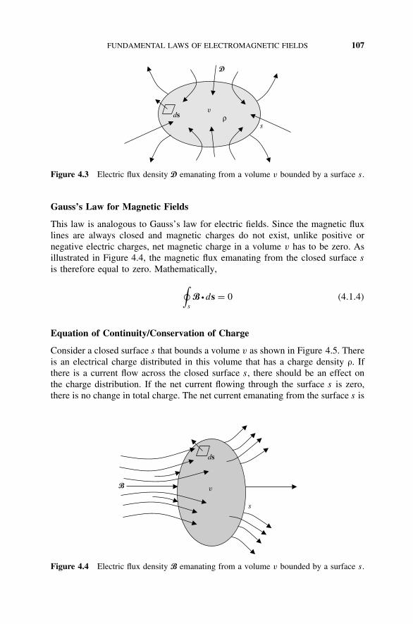
FUNDAMENTAL LAWS OF ELECTROMAGNETIC FIELDS 107
dss
ρ
Figure 4.3 Electric flux density D emanating from a volume v bounded by a surface s.
Gauss’s Law for Magnetic Fields
This law is analogous to Gauss’s law for electric fields. Since the magnetic fluxlines are always closed and magnetic charges do not exist, unlike positive ornegative electric charges, net magnetic charge in a volume v has to be zero. Asillustrated in Figure 4.4, the magnetic flux emanating from the closed surface s
is therefore equal to zero. Mathematically,
∮s
B ž ds = 0 (4.1.4)
Equation of Continuity/Conservation of Charge
Consider a closed surface s that bounds a volume v as shown in Figure 4.5. Thereis an electrical charge distributed in this volume that has a charge density ρ. Ifthere is a current flow across the closed surface s, there should be an effect onthe charge distribution. If the net current flowing through the surface s is zero,there is no change in total charge. The net current emanating from the surface s is
ds
s
Figure 4.4 Electric flux density B emanating from a volume v bounded by a surface s.

108 ELECTROMAGNETIC FIELDS AND WAVES
ds
sρ
Figure 4.5 Electric charges leaving a volume v bounded by a surface s.
equal to the time rate of decrease in the charge enclosed. Stated mathematically,∮s
J ž ds = − ∂
∂t
∫v
ρ dv (4.1.5)
Example 4.1 As shown in Figure 4.6, three arms of a rectangular conductingloop are fixed and the fourth is sliding in the x-direction with a velocity of500 m/s. The loop lies on the z = 0 plane, and there is a magnetic flux densityof 5 T in the z-direction. Find the emf induced in the loop. What happens if themagnetic flux varies with time as follows?
B = z ž 5 cos 109t T
SOLUTION∮c
E ž dl = − ∂
∂t
∫ x
0
∫ 2
0B ž z dx dy = − ∂
∂t(5 × 2 × x) = −10
dx
dt= −10 × 500
= −5000 V
x
y
x = 0 y = 0
y = 2 m
Figure 4.6

FUNDAMENTAL LAWS OF ELECTROMAGNETIC FIELDS 109
For the case of a magnetic field changing with time:
∮c
E ž dl = − ∂
∂t
∫ x
0
∫ 2
0B ž z dx dy = − ∂
∂t(2 × x × 5 cos 109t) V
= −2dx
dt5 cos 109t + 2 × x × 109 × 5 sin 109t V
= x × 1010 × sin 109t − 5000 cos 109t V
Example 4.2 An infinitely long solid cylindrical wire with its radius at 2 mis laying along the z-axis. It carries a current with its density given as J(ρ) =J0(1 − 0.5ρ)zA/m2. Find the magnetic field intensity inside as well as outsidethe wire.
SOLUTION From the condition given, it is clear that only the encircling mag-netic field Hφ exists. Hence, Ampere’s law for inside the wire gives
∮c
H ž dl =∫
s
J ž ds →∫ 2π
0Hφρ dφ =
∫ ρ
0
∫ 2π
0J0(1 − 0.5ρ′ dρ′ dφ)
or
2πρHφ = 2πJ0
(ρ2
2− 0.5
ρ3
3
)→ Hφ = J0
(ρ
2− ρ2
6
)A/m 0 ≤ ρ ≤ 2
Similarly, for outside the wire,
∮c
H ž dl =∫
s
J ž ds →∫ 2π
0Hφρ dφ =
∫ 2
0
∫ 2π
0J0(1 − 0.5ρ′ dρ′ dφ)
or
2πρHφ = 2πJ0
(22
2− 0.5
23
3
)→ Hφ = 2J0
3ρA/m 2 ≤ ρ
Equations (4.1.1)–(4.1.4) are known as Maxwell’s equations in integral (orlarge-scale) form. A differential (or point) form of these equations can beobtained via the application of the Stokes and Gauss theorems as follows.From (4.1.1), (4.1.2), and the Stokes theorem,
∮c
E ž dl =∫
s
(∇ × E) ž ds = − ∂
∂t
∫s
B ž ds → ∇ × E = −∂B
∂t
and∮c
H ž dl =∫
s
(∇ × H) ž ds =∫
s
J ž ds + ∂
∂t
∫s
D ž ds → ∇ × H = J + ∂D
∂t

110 ELECTROMAGNETIC FIELDS AND WAVES
Similarly, from (4.1.3), (4.1.4), and the Gauss theorem,∮s
D ž ds =∫
v
∇ ž D dv =∫
v
ρ dv → ∇ ž D = ρ
and ∮s
B ž ds =∫
v
∇ ž B dv = 0 → ∇ ž B = 0
Application of the Gauss theorem to (4.1.5) gives∮s
J ž ds =∫
v
∇ ž J dv = − ∂
∂t
∫v
ρ dv → ∇ ž J = −∂ρ
∂t
These results may be summarized as follows:
∇ × E = −∂B
∂t(4.1.6)
∇ × H = J + ∂D
∂t(4.1.7)
∇ ž D = ρ (4.1.8)
∇ ž B = 0 (4.1.9)
and
∇ ž J = −∂ρ
∂t(4.1.10)
Equations (4.1.6) to (4.1.9) are known as Maxwell’s equations in point (or dif-ferential) form; (4.1.10) is the equation of continuity in differential form.
Time-Harmonic Fields
Electromagnetic fields and sources considered up to this point were assumedto be an arbitrary function of time and space. The analysis can be simplifiedsignificantly with the assumption that these vary sinusoidally with time. It is tobe noted that this assumption includes a large number of cases. Further, thisformulation can be extended to include nonsinusoidal cases via Fourier series orFourier integrals, as necessary.
Consider a vector field A(r, t) that is sinusoidal with time. Using complexnotations, it can be expressed as
A(r, t) = A(r) cos(ωt + θ) = Re[A(r)ejθ]ejωt (4.1.11)
Therefore, the time derivative of this vector can be written as
∂
∂tA(r, t) = Re[jωA(r)ejθ]ejωt (4.1.12)

FUNDAMENTAL LAWS OF ELECTROMAGNETIC FIELDS 111
This indicates that a complex vector A(r)ejθ (a phasor quantity) can be used inplace of A(r, t), jω can replace the time derivative, and ejωt can be suppressedduring the field analysis. Further, it can be proved that division by jω will replacethe time integral. The time dependence can be recovered after multiplying thegiven complex vector by ejωt and then extracting the real part of that. This is afamiliar process used in ac circuit analysis to define the reactance of an inductoror a capacitor.
Using phasor representations for the field quantities, equations (4.1.6) to (4.1.10)can be written as follows:
∇ × E(r) = −jωB(r) (4.1.13)
∇ × H(r) = J(r) + jωD(r) (4.1.14)
∇ ž D(r) = ρ(r) (4.1.15)
∇ ž B(r) = 0 (4.1.16)
and
∇ ž J(r) = −jωρ(r) (4.1.17)
Bold roman symbols are now employed instead of bold script to distinguish thephasor field quantities. Further, to simplify the notation, space dependence of thefield quantities will no longer be included explicitly.
Constitutive Relations
A general analysis involves the evaluation of E, D, H, and B for given sources(current and charge densities). Maxwell’s equations represent only eight scalarequations, whereas unknown fields have 12 scalar components. Further, the twoGauss laws can be found from the other two Maxwell equations and the equationof continuity. Therefore, Maxwell’s equations give only six independent scalarequations, whereas 12 are needed to find 12 unknown field components. Theconstitutive relations provide the remaining six independent scalar equationsas follows:
D = ε0E + P (4.1.18)
where
P =
χeε0E for a linear mediumχeε0E for a linear and isotropic medium
(4.1.19)
P is the polarization density vector; ε0 the permittivity of the free space(8.854 × 10⁻¹² F/m), χe a dimensionless electrical susceptibility tensor, andχe a dimensionless electrical susceptibility scalar. Therefore, for a linear andisotropic medium,
D = ε0(1 + χe)E = εE = ε0εrE (4.1.20)
112 ELECTROMAGNETIC FIELDS AND WAVES
where εr is called the relative permittivity (or dielectric constant ) of the mediumand ε is its permittivity in F/m.
Similarly,B = µ0(H + M) (4.1.21)
where
M =
χmH for a linear mediumχmH for a linear and isotropic medium
(4.1.22)
M is the magnetization density vector, µ0 the permeability of the free space(4π × 10−7 H/m), χm a dimensionless magnetic susceptibility tensor, and χm
a dimensionless magnetic susceptibility scalar. Therefore, for a linear andisotropic medium,
B = µ0(1 + χm)H = µH = µ0µrH (4.1.23)
where µ is the permeability of the medium and µr is its relative permeability.Also, the current density term in (4.1.14) may have two parts, one due to an
impressed source and the other due to conduction. Conduction current densitycan be found via Ohm’s law as follows:
J = σE (4.1.24)
where σ is the conductivity of the medium in S/m. Therefore, (4.1.14) may beexpressed as follows:
∇ × H = Je + σE + jωε E = Je + jωε(
1 − jσ
ωε
)E = Je + jωε∗E (4.1.25)
where
ε∗ =(ε − j
σ
ω
)= ε(1 − j tan δ) → ε∗
r = ε
ε0− j
σ
ωε0= ε′ − jε′′ (4.1.26)
tan δ = σ
ωε(4.1.27)
J e is the impressed current source density, ε∗ the complex permittivity of thematerial, ε∗
r the complex relative permittivity, and tanδ is known as the losstangent. The loss tangent represents a ratio of the magnitude of conduction currentdensity to the magnitude of displacement current density in the medium.
Example 4.3 The electric field intensity in a source-free region is givenas follows:
E = z ž 4e−j (x−3y) V/m
If ε = ε0 and µ = µ0 in the region, find the signal frequency.

FUNDAMENTAL LAWS OF ELECTROMAGNETIC FIELDS 113
SOLUTION Since all electromagnetic fields must satisfy Maxwell’s equations,we first determine the corresponding magnetic field and then try to find theelectric field.
∇ × E = −jωµ0H → H = − 1
jωµ0
∣∣∣∣∣∣∣∣x y z∂
∂x
∂
∂y
∂
∂z
0 0 4e−j (x−3y)
∣∣∣∣∣∣∣∣= 12x + 4y
ωµ0e−j (x−3y)
and
∇ × H = jωε0E → E = 1
jωε0
∣∣∣∣∣∣∣∣∣∣∣
x y z
∂
∂x
∂
∂y
∂
∂z
12
ωµ0e−j (x−3y)
4
ωµ0e−j (x−3y) 0
∣∣∣∣∣∣∣∣∣∣∣= x0 + y0 + z
16
ω2µ0ε0e−j (x−3y)
Therefore,16
ω2µ0ε0= 4 → ω = 2√
µ0ε0= 6 × 10⁸ rad/s
Poynting’s Vector and the Power Flow
Poynting’s vector represents the electromagnetic power flow through a surface.The magnitude of Poynting’s vector represents the power per unit area leavingthat surface in the direction along the power flow (normal to that surface). Aninstantaneous Poynting vector can be evaluated for given instantaneous electricand magnetic field intensities as follows:
P = E × H (4.1.28)
A time-averaged Poynting’s vector can be determined from given phasor electricand magnetic field intensities as follows:
P = 12 Re(E × H∗) (4.1.29)
The asterisk on the magnetic field intensity represents its complex conjugate.
Example 4.4 The electromagnetic fields of an antenna at a large distance arefound as follows:
E(r, θ) = θj120π
r sin θcos
(π
2cos θ
)e−jk0r V/m

114 ELECTROMAGNETIC FIELDS AND WAVES
and
H(r, θ) = φj1
r sin θcos
(π
2cos θ
)e−jk0r A/m
Find the power radiated by this antenna.
SOLUTION
P = 1
2Re(E × H∗) = r
60π
r2 sin2 θcos2
(π
2cos θ
)W/m2
and
Pradiated =∫ π
0
∫ 2π
0P ž rr2 sin θ dθ dφ =
∫ π
0
∫ 2π
0
60π
sin θcos2
(π
2cos θ
)dθ dφ
= 1443.5 W = 1.4435 kW
4.2 THE WAVE EQUATION AND UNIFORM PLANEWAVE SOLUTIONS
In a source-free, linear, isotropic, homogeneous region, Maxwell’s curl equationsin phasor form are
∇ × E = −jωµH (4.2.1)
∇ × H = −jωε0ε∗E (4.2.2)
After taking the curl of (4.2.1) and substituting (4.2.2) on its right-hand side,we get
∇ ×∇ × E = −jωµ∇ × H = −jωµ(jωε0ε∗E) = k2E (4.2.3)
wherek = ω
√µε0ε∗ = β − jα (4.2.4)
k, α, and β being the wave number, attenuation constant, and phase constant,respectively.
Further,
∇ ×∇ × E = ∇(∇ ž E) − ∇2E = k2E → ∇2E + k2E = 0 (4.2.5)
Similarly, starting from (4.2.2), we find that
∇2H + k2H = 0 (4.2.6)
Equations (4.2.5) and (4.2.6) are known as the Helmholtz equation or vectorwave equation.
THE WAVE EQUATION AND UNIFORM PLANE WAVE SOLUTIONS 115
Consider an electric field that is directed along the x-axis (x-polarized). Further,it is uniform in the x and y directions (i.e., no variations with x or y). Therefore,the wave equation (4.2.5) for this case reduces to
d2Ex(z)
dz2+ k2Ex(z) = 0 (4.2.7)
This is an ordinary differential equation of second order, similar to (3.1.14). Itssolution can be found easily as follows:
Ex(z) = E+e−jkz + E−ejkz = E+e−αze−jβz + E−eαzejβz (4.2.8)
E+ and E− are integration constants. As noted in (3.1.18), the first term representsa wave traveling along +z (outgoing wave), and the second term represents awave traveling along −z (incoming wave).
Associated magnetic field intensity can be found from (4.2.2) instead of solv-ing (4.2.6). It can be proved that only the y-component of the magnetic fieldexists in this case. Therefore, the electric field, magnetic field, and direction ofwave propagation are orthogonal to each other. As before, the wavelength andphase velocity of the wave are
λ = 2π
β(4.2.9)
and
vp = ω
β(4.2.10)
The penetration depth of the wave is defined as a distance dp over which theamplitude of the electric field decays to 1/e of its value at z = 0. Hence,
dp = 1
α(4.2.11)
When the medium is highly conductive, the depth of penetration is called theskin depth, δ. It is found to be
δ =√
2
ωµσ(4.2.12)
The intrinsic impedance η of the medium, defined as
η =√
µ
ε∗ = Ex
Hy
= ωµ
k(4.2.13)

116 ELECTROMAGNETIC FIELDS AND WAVES
represents the ratio of electric field intensity component to magnetic field intensitycomponent transverse to the direction of wave propagation such that it has apositive real part.
Example 4.5 The electric field intensity of a time-harmonic field in free spaceis given as follows:
E = z(1 + j)e−j (2πx) mV/m
Assuming that the distance x is measured in meters, find (a) the wavelength,(b) the frequency, and (c) the associated magnetic field intensity.
SOLUTION
(a) λ = 2π
β= 2π
2π= 1 m
(b) f = 3 × 10⁸
λ= 3 × 10⁸ Hz = 300 MHz
(c) H = − 1
jωµ0∇ × E = − 1
jωµ0
∣∣∣∣∣∣∣∣x y z∂
∂x
∂
∂y
∂
∂z
0 0 Ez
∣∣∣∣∣∣∣∣= −y
2π
ωµ0(1 + j)e−j2πx mA/m
Alternatively, the intrinsic impedance can be used in conjunction with Poynt-ing’s vector to determine the associated magnetic field:
η = Ez
−Hy
= ωµ0
k= 2π × 3 × 108 × 4π × 10−7
2π= 376.9911
Example 4.6 A 10-kHz electromagnetic wave is being used to communicatebetween two submerged submarines. If the conductivity and dielectric constantof the seawater are 4 S/m and 81, respectively, find (a) the propagation con-stant, (b) the wavelength, (c) the attenuation constant, (d) the phase velocity,and (e) the skin depth of the wave.
SOLUTION Since the seawater is nonmagnetic, µ = µ0 and
k = ω√
µ0ε0ε∗ = ω
√µ0ε0
(εr − j
σ
ωε0
)
Further,σ
ωε0= 4
2π × 104 × 8.854 × 10−12= 7190.2 81

THE WAVE EQUATION AND UNIFORM PLANE WAVE SOLUTIONS 117
Therefore,
k ≈ ω
√µ0ε0
(−j
σ
ωε0
)=
√ωµ0σ
2− j
√ωµ0σ
2= 0.3974 − j0.3974 m−1
Hence, β = 0.3974 rad/m and α = 0.3974 Np/m.
λ = 2π
β= 2π
0.3974= 15.8107 m
vp = ω
β= 2π × 104
0.3974= 15.8107 × 10⁴ m/s
and
δ = 1
α= 1
0.3974= 2.5163 m
Uniform Plane Wave Propagating Along r
The preceding analysis can be extended easily for the case of a wave that propa-gates at an angle from a given axis. Consider a uniform plane wave propagatingalong r at an angle θ from the z-axis, as illustrated in Figure 4.7. This wave hasan x-component of the electric field intensity that can be written as
E = xE0e−jkr r (4.2.13)
Since the magnetic field intensity must be orthogonal to both its electric field andthe direction of propagation, it will have a y as well as a z component. We selecta point B at r on the propagation path and drop a perpendicular from that onthe y-axis. Further, we drop a perpendicular from point C to A in the direction
z
y
r
A
B
CO
θ θ
Figure 4.7 Geometry for a uniform plane wave propagating at an angle θ from the z-axis.

118 ELECTROMAGNETIC FIELDS AND WAVES
of propagation. As indicated in Figure 4.7, the angle ABC is equal to θ as well.Assume that the Cartesian coordinates of point B are y and z. Hence,
r = OA + AB = OC sin θ + BC cos θ = y sin θ + z cos θ (4.2.14)
and
krr = kr sin θ y + kr cos θ z = kyy + kzz (4.2.15)
where
ky = kr sin θ
and
kz = kr cos θ
Therefore, (4.2.13) may be written as
E = xE0e−j (kyy+kzz) (4.2.16)
Phase velocities vpy and vpz of this wave with respect to the y and z axes canbe found as
vpy = ω
Re(ky)(4.2.17)
and
vpz = ω
Re(kz)(4.2.18)
Example 4.7 The electric field intensity of a time-harmonic wave traveling ina source-free free space is given as follows:
E = (4y + 3z)e−j (6y−8z) mV/m
Assuming that y and z represent their respective distances in meters, determine(a) the angle of the propagation direction relative to the z-axis, (b) the wave-lengths of the wave along the r , y, and z directions, (c) the phase velocities alongthe r , y, and z directions, (d) the energy velocities along the r , y, and z directions,(e) the frequency of the wave, and (f) the associated magnetic field intensity.
SOLUTION From the information given, ky = k sin θ = 6 and kz = k cos θ = 8.Therefore,
kr =√
k2y + k2
z =√
62 + 82 = 10 m−1
(a) sin θ = ky
kr
= 0.6 → θ = 36.87

BOUNDARY CONDITIONS 119
An analysis of the given electric field indicates that this angle is from the −z
direction, and therefore it should be subtracted from 180 to obtain the anglemeasured from +z. Hence, θ = 180 − 36.87 = 143.13.
(b) λr = 2π
kr
= 2π
10= 0.6283 m, λy = 2π
ky
= 2π
6= 1.0472 m, and λz = 2π
kz
= 2π
8= 0.7854 m
(c) Since the wave is propagating in free space, its phase velocity along r is3 × 108 m/s. The frequency of this wave may be found as follows:
ω = vrkr = 3 × 10⁹ rad/s or f = 3 × 10⁸
λr
Hz = 477.47 MHz
vpy = ω
ky
= 3 × 10⁹
6= 5 × 10⁸ m/s
and
vpz = ω
kz
= 3 × 10⁹
8= 3.75 × 10⁸ m/s
(d) ver = 3 × 10⁸ m/s, vey = ver sin θ = 1.8 × 10⁸ m/s, and vez = ver cos θ =2.4 × 10⁸ m/s
(e) The frequency is 477.47 MHz, as found in part (c).
(f) H = − 1
jωµ0∇ × E = − 1
jωµ0
∣∣∣∣∣∣∣∣x y z∂
∂x
∂
∂y
∂
∂z
0 Ey Ez
∣∣∣∣∣∣∣∣= x ž 13.2629 × 10⁻⁶e−j (6y−8z) A/m
4.3 BOUNDARY CONDITIONS
The electromagnetic field problems considered so far have involved a singlemedium of infinite extent. However, there are numerous real-world problemsthat require analysis of electromagnetic fields in the presence of more than onemedium. Therefore, it is important to know the behavior of electromagnetic fieldsacross the interface of two media.
Consider an interface of the two media, as illustrated in Figure 4.8. The elec-trical characteristics of these media are as indicated. When (4.1.2) is applied toan infinitesimal area across the interface and its side h is reduced to zero underthe limit, it results in the relation
(H2 − H1) × n = Js (4.3.1)

120 ELECTROMAGNETIC FIELDS AND WAVES
∆w∆h
Medium 1
Medium 2 µ1,ε1
µ2,ε2
n
Figure 4.8 Infinitesimal area across the interface of medium 1 and medium 2.
where subscripts 1 and 2 are used to indicate the magnetic field intensity in thecorresponding medium. Js represents the surface current density in A/m on theboundary, and the unit vector n is directed into medium 1.
Similarly, when (4.1.1) is applied to this infinitesimal area across the interfaceand its side h is reduced to zero under the limit, it results in the relation
n× (E2 − E1) = 0 (4.3.2)
Subscripts 1 and 2 are used to indicate the electric field intensity in the corre-sponding medium. Now, consider a pillbox volume across the interface of thetwo media, as shown in Figure 4.9. When (4.1.3) is applied to this volume andthe side h is reduced to zero under the limit, it results in the relation
n ž (D1 − D2) = ρs (4.3.3)
where subscripts 1 and 2 are used to indicate the electric flux density in thecorresponding medium ρs represents the surface charge density in C/m2 on theboundary, and the unit vector n is directed into medium 1.
Similarly, the following relation is found via (4.1.4) for the magnetic fluxdensities in the two media:
n ž (B1 − B2) = 0 (4.3.4)
Equations (4.3.1) to (4.3.4) can be used to determine the electromagnetic fieldsfrom one to other medium across the boundary. It is to be noted that (4.3.3)
∆s
∆h
Medium 1
Medium 2 µ1,ε1
µ2,ε2
n
Figure 4.9 Pillbox volume across the interface of medium 1 and medium 2.

BOUNDARY CONDITIONS 121
and (4.3.4) are formulated via Gauss’s laws that are not independent, and there-fore these conditions are satisfied automatically if (4.3.1) and (4.3.2) are met.Further, if medium 2 is a perfect conductor, the fields inside it vanish, andtherefore the boundary conditions (4.3.1) to (4.3.4) reduce to
n× H1 = Js (4.3.5)
n× E1 = 0 (4.3.6)
n ž D1 = ρs (4.3.7)
and
n ž B1 = 0 (4.3.8)
If the second medium is a good conductor (finite conductivity), the fields penetratemostly up to its skin depth. In such a case, the following Leontovich impedanceboundary condition can be used provided that the radius of curvature of thesurface is significantly greater than the skin depth (2/ ωµσ)1/2.
Et = Zs(n × H) (4.3.9)
where
Zs =√
µ
ε≈
√jµω
σ(4.3.10)
Example 4.8 The region x > 0 is a perfect dielectric with εr = 2.25, and theregion x < 0 is a free space. At the interface, subscript 1 denotes field componentson the +x side of the boundary and subscript 2 those on the −x side. If D1 =x + 2yC/m2, find D2, E1, and E2.
SOLUTION The conditions stated in the problem are illustrated in Figure 4.10.The interface is x = 0 plane, and therefore the x component, will be normal, with
Medium 2 Medium 1Free space
εr = 2.25
x
z
y
Figure 4.10 Conditions for Example 4.8.

122 ELECTROMAGNETIC FIELDS AND WAVES
the y component tangential to this plane.
D1 = ε1E1 → E1 = D1
ε1= 1
2.25ε0x + 2
2.25ε0y V/m
From the boundary conditions, the x component of electric flux density and y
component of electric field intensity in medium 2 will be same as in medium1. Hence,
D2x = 1 and E2y = 2
2.25ε0
Therefore,
D2 = x + 2
2.25y C/m2
and
E2 = D2
ε0= 1
ε0x + 2
2.25ε0y V/m
Example 4.9 A sphere of 2 m radius is made of a perfect dielectric material(medium 1). It is surrounded by free space (medium 2). Electric field intensitiesin the two media are given as follows:
E1 = E01(cos θr − sin θθ) r ≤ 2 m
and
E2 = E02
[(1 + 8
r3
)cos θr −
(1 − 4
r3
)sin θθ
]r ≥ 2 m
Find the permittivity of the spherical medium.
SOLUTION As indicated in Figure 4.11, the r components of the electric fieldsare normal and the θ components are tangential at the interface. Therefore,
− sin θE01 = −(
1 − 4
8
)sin θE02 → E02 = 2E01
x
y
z
r
θ
φ
Figure 4.11 Conditions for Example 4.9.

UNIFORM PLANE WAVE INCIDENT NORMALLY ON AN INTERFACE 123
and
ε1E01 cos θ = ε0E02 ž 2 cos θ → ε1 = 2ε0E02
E01= 4ε0 F/m
4.4 UNIFORM PLANE WAVE INCIDENT NORMALLYON AN INTERFACE
Consider a uniform plane electromagnetic wave propagating in medium 1 asillustrated in Figure 4.12. The electric field Ei of this wave is y directed, and itsmagnetic field Hi is in the −x direction. A wave propagating in the +z directionis incident normally on the interface of medium 2 with medium 1. The electricalcharacteristics of the two media are as indicated in Figure 4.12. Since the waveexperiences a change in electrical characteristics in its path, a part of the incidentsignal is reflected back, while the remaining signal is transmitted into medium 2.Thus, there are two waves in medium 1 propagating in opposite directions, andone in medium 2 that continues along +z.
The electromagnetic fields associated with the incident wave can be expressedas follows:
Ei = yE0e−jk1z (4.4.1)
and
Hi = −xH0e−jk1z = −x
E0
η1e−jk1z (4.4.2)
x
z
y
Hi Hr Ht
Ei
Et
Er
Medium 1σ1,ε1,µ1
Medium 2σ2,ε2,µ2
Figure 4.12 Geometry of a uniform plane wave incident normally on the interface oftwo media.

124 ELECTROMAGNETIC FIELDS AND WAVES
where E0 and H0 are arbitrary constants, k1 the complex wave number, and η1
the complex intrinsic impedance of medium 1.Similarly, electromagnetic fields associated with the reflected wave (Er and
Hr ) as well as the transmitted wave (Et and Ht ) can be expressed as follows:
Er = yRE 0e+jk1z (4.4.3)
Hr = xRH 0e−jk1z = xR
E0
η1e+jk1z (4.4.4)
Et = yTE 0e−jk2z (4.4.5)
and
Ht = −xTH 0e−jk1z = −xT
E0
η2e−jk2z (4.4.6)
where R and T are complex reflection and transmission coefficients, respec-tively, k2 the complex wave number in medium 2, and η2 the complex intrinsicimpedance of medium 2.
Now, applying the boundary conditions (tangential components of the fieldsare continuous across the boundary) at z = 0 gives
E0 + RE 0 = TE 0 → 1 + R = T (4.4.7)
and
−E0
η1+ R
E0
η1= −T
E0
η1→ 1 − R = η1
η2T (4.4.8)
Equations (4.4.7) and (4.4.8) can be solved for R and T as follows:
T = 2η2
η1 + η2(4.4.9)
and
R = η2 − η1
η1 + η2(4.4.10)
Therefore, the total electric field at any point in medium 1 is found to be
E1 = yE0e−jk1z + yRE 0e
+jk1z
|E1|2 = |E0|2[e−2α1z + ρ2e2α1z + 2ρ cos(2β1z + θ)] (4.4.11)
where
R = ρejθ (4.4.12)
k1 = β1 − jα1 (4.4.13)

UNIFORM PLANE WAVE INCIDENT NORMALLY ON AN INTERFACE 125
β1 is the phase constant in rad/s and α1 is the attenuation constant in Np/m formedium 1.
It is to be noted that the propagation characteristics of this wave are very muchsimilar to that of a wave propagating on the transmission line, as discussed inChapter 3.
Example 4.10 The electric field intensity of a uniform plane wave propagatingin free space is given as
Ei (z, t) = y ž 4.8 cos(109t − k0z) V/m
If this wave impinges normally on a lossless medium (µr = 1 and εr = 2.25) inthe z ≥ 0 region, find k0, k2, R, T , the VSWR, and the average power transmittedinto the medium.
SOLUTION The wave numbers and intrinsic impedance of the wave in the twomedia are found as follows:
k0 = ω√
µ0ε0 = 109√
4π × 10−7 × 8.854 × 10−12 = 3.3356 rad/m
k2 = ω√
µ0ε0εr = k0
√2.25 = 5.0034 rad/m
η1 =√
µ0
ε0=
√4π × 10−7
8.854 × 10−12= 376.7343
and
η2 =√
µ0
ε0εr
=√
4π × 10−7
8.854 × 10−12 × 2.25= 251.1562
Now R and T can be found via (4.4.9) and (4.4.10) as
R = η2 − η1
η1 + η2≈ −0.2
and
T = 2η2
η1 + η2≈ 0.8
The VSWR in medium 1 is found to be
VSWR = 1 + ρ
1 − ρ= 1 + 0.2
1 − 0.2= 1.5
The electric field intensity in medium 2 is
Et (z, t) = y ž 3.84 cos(109t − k2z) V/m

126 ELECTROMAGNETIC FIELDS AND WAVES
Therefore, the time-averaged power transmitted into medium 2 may be foundas follows:
Pav = 1
2Re(E × H∗) = 1
2
|Et |2η2
= 1
2
(3.842
251.1562
)= 0.0294 W/m2
4.5 MODIFIED MAXWELL’S EQUATIONS AND POTENTIALFUNCTIONS
Equation (4.1.9) implies that the magnetic flux does not start from or terminateat a magnetic charge the way that electric flux does with electric charge. Thisis because there is no real magnetic charge (or magnetic monopole). In fact,the smallest unit of the magnetic source is a magnetic dipole that is actually aninfinitesimal current loop.
Consider a general case where the source consists of two types of currents:a linear current that flows or oscillates in the linear direction, and an infinitesi-mal circulatory current that flows or oscillates around an infinitesimal loop. Forthis case it is rather hard to describe mathematically the electric current den-sity J that includes both parts. Mathematically, it is sometimes advantageousto recognize its linear part as electric current Je and imagine its infinitesimalcirculatory current as an equivalent magnetic dipole source. If the circulatorycurrent varies in magnitude and direction or oscillates around the loop withtime, the equivalent magnetic dipole strength also oscillates with time. Whenthe magnetic dipole oscillates with time, it can be considered as an imagi-nary magnetic current flowing up and down. This is completely analogous toa time-varying electric dipole. Therefore, a time-varying circulatory current canbe represented by an equivalent magnetic current and charges, Jm and ρm,respectively.
Imagine now that the magnetic charge ρm produces a magnetic flux, analogousto the electric charge ρe producing the electric flux. Then equation (4.1.9) shouldbe modified to
∇ ž B = ρm
If (4.1.9) is modified, (4.1.6) also needs modification because divergence of thecurl of a vector is always zero, which is not true because ρm is a function oftime:
∇ ž (∇ × E) = −∇ ž∂B
∂t= − ∂
∂t(∇ ž B) = − ∂
∂tρm = 0
If it is assumed that the usual continuity equation should hold between ρm and Jm,
∇ ž Jm = −∂ρm
∂t
Hence, equation (4.1.6) should be modified to
∇ × E = −Jm − ∂B
∂t

MODIFIED MAXWELL’S EQUATIONS AND POTENTIAL FUNCTIONS 127
Therefore, the modified Maxwell’s equations for the time-harmonic field and thetwo continuity equations can be expressed as:
∇ × E(r) = −Jm(r) − jωB(r) (4.5.1)
∇ × H(r) = Je(r) + jω D(r) (4.5.2)
∇ ž D(r) = ρe(r) (4.5.3)
∇ ž B(r) = ρm(r) (4.5.4)
∇ ž Je(r) = −jωρe(r) (4.5.5)
and
∇ ž Jm(r) = −jωρm(r) (4.5.6)
Magnetic Vector and Electric Scalar Potentials
Potential functions are introduced to transform Maxwell’s equations mathemati-cally and so facilitate solutions to electromagnetic problems. Consider that thereare only electric sources (current and charge) present in a volume under consider-ation (i.e., Je = 0, ρe = 0, Jm = 0, and ρm = 0). Therefore, Maxwell’s equationsfor time-harmonic fields and the equation of continuity can be written as follows:
∇ × E = −jωB (4.5.7)
∇ × H = Je + jωD (4.5.8)
∇ ž D = ρe (4.5.9)
∇ ž B = 0 (4.5.10)
and
∇ ž Je = −jωρe (4.5.11)
As defined earlier, the constitutive relations are
B = µH (4.5.12)
and
D = εE (4.5.13)
Since divergence of the curl of a vector is always zero, the magnetic flux densityin (4.5.10) may be assumed to be the curl of vector A. Hence,
∇ ž B = 0 ⇒ B = ∇ × A (4.5.14)
128 ELECTROMAGNETIC FIELDS AND WAVES
Substitution of B from (4.5.14) into (4.5.7), and recognizing the fact that the curlof the gradient of a scalar is always zero gives
∇ × E = −jω∇ × A ⇒ ∇×(E + jωA) = 0 ⇒ E + jωA = −∇φe
Therefore,E = −∇φe − jωA (4.5.15)
where A is called the magnetic vector potential and φe is known as the electricscalar potential.
Using (4.5.12), (4.5.13), and (4.5.15), (4.5.8) may be written as
∇×∇ × Aµ
= Je + jωεE = Je + jωε(−∇φe − jωA)
If µ is not changing with space coordinates, this relation simplifies furtheras follows:
∇ × ∇ × A = ∇(∇ ž A) − ∇2A = µJe − jωεµ∇φe + ω2µεA
or
∇2A + ω2µεA = −µJe + jωεµ∇φe + ∇(∇ ž A)
or
∇2A + ω2µεA = −µJe + ∇(∇ ž A + jωεµφe) (4.5.16)
Similarly for ε not changing with space coordinates, (4.5.9), (4.5.13),and (4.5.15) give
∇ ž (−∇φe − jωA) = ρe
ε→ ∇2φe + jω(∇ ž A) = −ρe
ε(4.5.17)
Equations (4.5.16) and (4.5.17) represent a pair of coupled partial differentialequations for φ and A. These may be uncoupled via Helmholtz’s theorem, whichstates that a vector is specified completely by its curl and divergence. Since onlythe curl of A is defined via (4.5.14), we are at liberty to specify its divergence.The Lorentz condition may be used to define it as
∇ ž A = −jωεµφe (4.5.18)
Thus, (4.5.16) and (4.5.17) simplify to
∇2A + k2A = −µJ (4.5.19)
and
∇2φe + k2φe = −ρe
ε(4.5.20)

MODIFIED MAXWELL’S EQUATIONS AND POTENTIAL FUNCTIONS 129
where k2 = ω2µε and k is the wave number. It should be noted at this point thatthe continuity equation is implied by the Lorentz condition.
Electric Vector and Magnetic Scalar Potentials
Electric vector and magnetic scalar potentials are introduced when the existenceof only magnetic current and charge is assumed in the region (i.e, ρe = 0 andJe = 0). Therefore, Maxwell’s equations and the equation of continuity for thiscase are found to be
∇ × E = −Jm − jωB (4.5.21)
∇ × H = jωD (4.5.22)
∇ ž D = 0 (4.5.23)
∇ ž B = ρm (4.5.24)
and
∇ ž Jm = −jωρm (4.5.25)
As before, D = εE and B = µH. Because of (4.5.23), it is assumed that
D = −∇ × F (4.5.26)
where F is called the electric vector potential.After substituting (4.5.26) into (4.5.22) and noting that curl of the gradient of
a scalar is always zero, we get
∇ × H = −jω∇ × F → ∇×(H + jωF) = 0 → H + jωF = −∇φm
Therefore,H = −∇φm − jωF (4.5.27)
where φm is called the magnetic scalar potential. Now, from (4.5.21), (4.5.26),and (4.5.27),
∇×(
−∇ × Fε
)= −Jm − jωµ(−∇φm − jωF)
or
−∇ × ∇ × F = −εJm + jωµε∇φm − ω2µεF
or
−[∇(∇ ž F) − ∇2F] + ω2µεF = −εJm + jωµε∇φm (4.5.28)

130 ELECTROMAGNETIC FIELDS AND WAVES
As in the preceding case, if the Lorentz condition
∇ ž F = −jωµεφm (4.5.29)
is introduced, then∇2F + ω2µεF = −εJm (4.5.30)
Further, (4.5.24), (4.5.27), and (4.5.29) give
∇ ž [µ(−∇φm − jωF)] = ρm ⇒ −∇2φm − jω(−jωµεφm) = ρm
µ
or
∇2φm + ω2µεφm = −ρm
µ(4.5.31)
An electromagnetic field problem can be divided into these two cases, solved foreach case, and the individual solutions can be superimposed to find the completesolution. Thus, the electromagnetic fields may be found easily after determin-ing the vector potentials via (4.5.19) and (4.5.30) and the corresponding Lorentzconditions. This procedure is used in the following section to further formulategeneral solution techniques for source-free cases that are specialized subsequentlyfor a few waveguides.
4.6 CONSTRUCTION OF SOLUTIONS
The analysis presented in Section 4.5 is specialized here for a source-free regionwith rectangular as well as cylindrical coordinates. It is further divided into twocases; the electric vector potential is assumed to be zero in one, and the magneticvector potential, zero in the other.
Rectangular Coordinate System
1. Assume that A = zAz and F = 0; then (4.5.14), (4.5.15), and (4.5.18) give
H = 1
µ∇×zAz = 1
µ
[x
∂Az
∂y+ y
(−∂Az
∂x
)+ z0
](4.6.1)
and
E = −jωzAz + 1
jωµε∇ ∂Az
∂z(4.6.2)
For this case, (4.5.19) simplifies to
∇2Az + k2Az = 0 → ∂2Az
∂x2+ ∂2Az
∂y2+ ∂2Az
∂z2+ k2Az = 0 (4.6.3)

CONSTRUCTION OF SOLUTIONS 131
After (4.6.3) is solved for a given problem, field components are foundfrom (4.6.1) and (4.6.2) as follows:
Hx = 1
µ
∂Az
∂y(4.6.4)
Hy = − 1
µ
∂Az
∂x(4.6.5)
Hz = 0 (4.6.6)
Ex = 1
jωµε
∂2Az
∂x∂z(4.6.7)
Ey = 1
jωµε
∂2Az
∂y∂z(4.6.8)
and
Ez = 1
jωµε
(∂2
∂z2+ k2
)Az (4.6.9)
Since the magnetic fields are transverse to the z-axis (Hz = 0), these fields areknown as TMz (transverse magnetic to z ) mode fields.
2. Assume that F = zFz and A = 0; then (4.5.26) and (4.5.27) give
E = −1
ε∇×zFz = −1
ε
[x
∂Fz
∂y+ y
(−∂Fz
∂x
)+ z0
](4.6.10)
and
H = −jωzFz + 1
jωµε∇ ∂Fz
∂z(4.6.11)
For this case, (4.5.30) simplifies to
∇2Fz + k2Fz = 0 → ∂2Fz
∂x2+ ∂2Fz
∂y2+ ∂2Fz
∂z2+ k2Fz = 0 (4.6.12)
After (4.6.12) is solved for a given problem, field components are foundfrom (4.6.10) and (4.6.11) as follows:
Ex = −1
ε
∂Fz
∂y(4.6.13)
Ey = 1
ε
∂Fz
∂x(4.6.14)
Ez = 0 (4.6.15)
Hx = 1
jωµε
∂2Fz
∂x ∂z(4.6.16)

132 ELECTROMAGNETIC FIELDS AND WAVES
Hy = 1
jωµε
∂2Fz
∂y∂z(4.6.17)
and
Hz = 1
jωµε
(∂2
∂z2+ k2
)Fz (4.6.18)
Since the electric fields are transverse to the z-axis in this case, these fields areknown as TE z (transverse electric to z ) mode fields.
Cylindrical Coordinate System
1. Assume that A = zAz and F = 0; then from (4.5.14), (4.5.15), and (4.5.18),we get
H = 1
µ∇×zAz = 1
µ
[ρ
1
ρ
∂Az
∂φ+ φ
(−∂Az
∂ρ
)+ z0
](4.6.19)
and
E = −jωzAz + 1
jωµε∇ ∂Az
∂z(4.6.20)
For this case, (4.5.19) in cylindrical coordinates may be written as follows:
∇2Az + k2Az = 0 → 1
ρ
∂
∂ρ
(ρ∂Az
∂ρ
)+ 1
ρ2
∂2Az
∂φ2+ ∂2Az
∂zz+ k2Az = 0 (4.6.21)
Once solutions to (4.6.21) are found, electromagnetic fields may be determinedfrom (4.6.19) and (4.6.20) as follows:
Hρ = 1
µρ
∂Az
∂φ(4.6.22)
Hφ = − 1
µ
∂Az
∂ρ(4.6.23)
Hz = 0 (4.6.24)
Eρ = 1
jωµε
∂2Az
∂ρ∂z(4.6.25)
Eφ = 1
jωµερ
∂2Az
∂φ∂z(4.6.26)
and
Ez = 1
jωµε
(∂2
∂z2+ k2
)Az (4.6.27)

METALLIC PARALLEL-PLATE WAVEGUIDE 133
This is the TMz mode (magnetic field transverse to the z-axis) in a cylindricalcoordinate system.
2. For F = zFz and A = 0, (4.5.26) and (4.5.27) in cylindrical coordinates give
E = −1
ε∇×zFz = −1
ε
[ρ
1
ρ
∂Fz
∂φ+ φ
(−∂Fz
∂ρ
)+ z0
](4.6.28)
and
H = −jωzFz + 1
jωµε∇
(∂Fz
∂z
)(4.6.29)
Further, (4.5.30) reduces to
∇2Fz + k2Fz = 0 → 1
ρ
∂
∂ρ
(ρ∂Fz
∂ρ
)+ 1
ρ2
∂2Fz
∂φ2+ ∂2Fz
∂z2+ k2Fz = 0 (4.6.30)
After (4.6.30) is solved, the field components are determined from (4.6.28) and(4.6.29) as follows:
Eρ = − 1
ερ
∂Fz
∂φ(4.6.31)
Eφ = 1
ε
∂Fz
∂ρ(4.6.32)
Ez = 0 (4.6.33)
Hρ = 1
jωµε
∂2Fz
∂ρ∂z(4.6.34)
Hφ = 1
jωµερ
∂2Fz
∂φ ∂z(4.6.35)
and
Hz = 1
jωµε
(∂2
∂z2+ k2
)Fz (4.6.36)
This is the TEz mode (electric field transverse to the z-axis) in a cylindricalcoordinate system.
These formulations are used in the following sections to analyze propagationof electromagnetic signals through the waveguide.
4.7 METALLIC PARALLEL-PLATE WAVEGUIDE
Consider a parallel-plate waveguide that consists of two perfectly conductiveplates extending to infinity on the y –z plane, as illustrated in Figure 4.13. Sep-aration between the two plates is assumed to be a. There is an electromagnetic
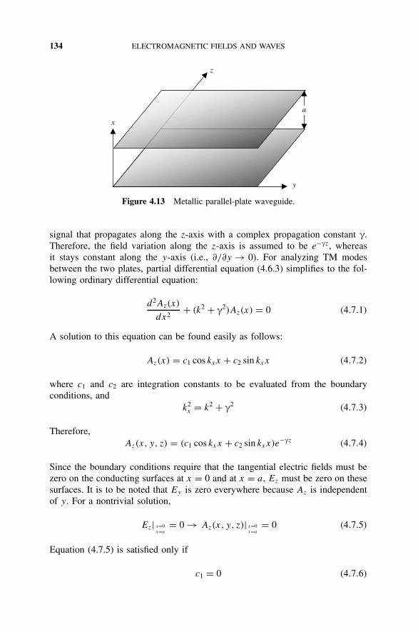
134 ELECTROMAGNETIC FIELDS AND WAVES
y
x
z
a
Figure 4.13 Metallic parallel-plate waveguide.
signal that propagates along the z-axis with a complex propagation constant γ.Therefore, the field variation along the z-axis is assumed to be e−γz, whereasit stays constant along the y-axis (i.e., ∂/∂y → 0). For analyzing TM modesbetween the two plates, partial differential equation (4.6.3) simplifies to the fol-lowing ordinary differential equation:
d2Az(x)
dx2+ (k2 + γ2)Az(x) = 0 (4.7.1)
A solution to this equation can be found easily as follows:
Az(x) = c1 cos kxx + c2 sin kxx (4.7.2)
where c1 and c2 are integration constants to be evaluated from the boundaryconditions, and
k2x = k2 + γ2 (4.7.3)
Therefore,Az(x, y, z) = (c1 cos kxx + c2 sin kxx)e−γz (4.7.4)
Since the boundary conditions require that the tangential electric fields must bezero on the conducting surfaces at x = 0 and at x = a, Ez must be zero on thesesurfaces. It is to be noted that Ey is zero everywhere because Az is independentof y. For a nontrivial solution,
Ez| x=0x=a
= 0 → Az(x, y, z)| x=0x=a
= 0 (4.7.5)
Equation (4.7.5) is satisfied only if
c1 = 0 (4.7.6)

METALLIC PARALLEL-PLATE WAVEGUIDE 135
andkx = mπ
a, m = 0, 1, 2, . . . (4.7.7)
Therefore,Az = c2 sin
(mπ
ax)
e−γz (4.7.8)
Further, the propagation constant can be found from (4.7.3) as follows:
γ =√(mπ
a
)2 − k2 (4.7.9)
Therefore, the signal will propagate without attenuation if k > mπ/a, and it willattenuate for k < mπ/a. The cutoff occurs at k = mπ/a.
Once Az is determined, the field components may be found from (4.6.4)–(4.6.9)as follows:
Hx = 0 (4.7.10)
Hy = −c2
µ
mπ
acos
(mπ
ax)
e−γz (4.7.11)
Hz = 0 (4.7.12)
Ex = −c2γ
jωµε
mπ
acos
(mπ
ax)
e−γz (4.7.13)
Ey = 0 (4.7.14)
and
Ez = c2
jωµε
(mπ
a
)2sin
(mπ
ax)
e−γz (4.7.15)
These results are summarized in Table 4.1 assuming that −c2(kc/µ) = E0.A similar procedure may be used to determine the characteristics of TE
mode fields propagating through this waveguide. Final results are summarized inTable 4.1.
Example 4.11 A metallic parallel-plate waveguide is air-filled, and the sepa-ration between its plates is 4.5 cm. Investigate the characteristics of a 12-GHzsignal propagating in TMm0 modes.
SOLUTION
kc = mπ
a→ λc = 2π
kc
= 2a
m= 2 × 4.5 × 10−2
mm
and
fc = 3 × 10⁸
λc
= 3 × 10⁸ × m
9 × 10⁻²Hz = 3.3333m GHz

136 ELECTROMAGNETIC FIELDS AND WAVES
TABLE 4.1 Signal Propagation in Parallel-Plate Waveguides
TEm0 Modes TMm0 Modes
kc
mπ
a
mπ
a
γm0
√k2c − k2
0
√k2c − k2
0
Hz(x, z) − kc
jωµH0 cos(kcx)e−γm0z 0
Ez(x, z) 0 jE0kc
ωεsin(kca)e−γm0z
Hx(x, z) − γm0
jωµH0 sin(kcx)e−γm0z 0
Hy(x, z) 0 E0 cos(kcx)e−γm0z
Ex(x, z) 0γm0
jωεE0 cos(kcx)e−γm0z
Ey(x, z) H0 sin(kcx)e−γm0z 0
Hence, the cutoff frequencies for first four TM modes are found as follows:
TM10 → fc = 3.3333 GHz
TM20 → fc = 6.6667 GHz
TM30 → fc = 10 GHz
TM40 → fc = 13.3333 GHz
Since the cutoff frequency for the TM40 mode is higher than the signal fre-quency of 12 GHz, only TM10, TM20, and TM30 modes will exist for this sig-nal. The corresponding cutoff wavelengths are 9, 4.5, and 3 cm, respectively.The signal wavelength inside the guide for each mode can be found as fol-lows:
TM10 → λg = λ0√1 − (λ0/λc)
2= 2.5√
1 − (2.5/9)2cm = 2.6024 cm
TM20 → λg = λ0√1 − (λ0/λc)
2= 2.5√
1 − (2.5/4.5)2cm = 3.0067 cm
and
TM30 → λg = λ0√1 − (λ0/λc)
2= 2.5√
1 − (2.5/3)2cm = 4.5227 cm

METALLIC RECTANGULAR WAVEGUIDE 137
4.8 METALLIC RECTANGULAR WAVEGUIDE
In this section we present another application of the formulation described inSection 4.6 to analyze the electromagnetic signals propagating through a hol-low metallic cylindrical waveguide of rectangular cross section, as shown inFigure 4.14. Both the geometry of a rectangular waveguide and the coordinatesystem are shown. It is assumed that its cross section is a × b, and the electromag-netic signal is propagating along the z-axis. Therefore, the field variation alongthe z-axis is given as e−jkzz. TM and TE modes propagating through this waveg-uide can be analyzed using equations (4.6.1) to (4.6.18). For TE modes, (4.6.12)reduces to
∂2Fz(x, y)
∂x2+ ∂2Fz(x, y)
∂y2+ (k2 − k2
z )Fz(x, y) = 0 (4.8.1)
It is a second-order partial differential equation that can be solved using theseparation-of-variables technique as follows.
Assume that Fz(x, y) is a product of two functions, one dependent on x onlyand the other on y only. Hence,
Fz(x, y) = f1(x)f2(y) (4.8.2)
Therefore,
∂2Fz(x, y)
∂x2= f2(y)
d2f1(x)
dx2(4.8.3)
and
∂2Fz(x, y)
∂y2= f1(x)
d2f2(y)
dy2(4.8.4)
Substituting (4.8.2) to (4.8.4) into (4.8.1) and rearranging results in
1
f1(x)
d2f1(x)
dx2+ 1
f2(y)
d2f2(y)
dy2= −(k2 − k2
z ) (4.8.5)
x
y
zb
a
Figure 4.14 Metallic rectangular waveguide.

138 ELECTROMAGNETIC FIELDS AND WAVES
In (4.8.5), the first term is only x dependent, the second is dependent on y
only, and the sum of these two is always a constant, as its right-hand side indi-cates. Therefore, each term on the left-hand side must be independently constantas follows:
1
f1(x)
d2f1(x)
dx2= −k2
x (4.8.6)
and
1
f2(y)
d2f2(y)
dy2= −k2
y (4.8.7)
where kx and ky are constants.Equations (4.8.6) and (4.8.7) are in the form of the harmonic equation consid-
ered earlier, and its solutions are the harmonic functions. Complete solutions toeach of these can be written as
f1(x) = c1 cos kxx + c2 sin kxx (4.8.8)
and
f2(y) = c3 cos kyy + c4 sin kyy (4.8.9)
Therefore, the solution to (4.8.1) is found to be
Fz(x, y) = (c1 cos kxx + c2 sin kxx)(c3 cos kyy + c4 sin kyy) (4.8.10)
Further, equations (4.8.1), (4.8.6), and (4.8.7) give the separation equation,
k2x + k2
y + k2z = k2 (4.8.11)
Since tangential electric fields must be zero on the conducting surfaces, theboundary conditions for (4.8.1) are found to be
Ex| y=0y=b
= 0 → ∂Fz
∂y
∣∣∣∣y=0y=b
= 0 (4.8.12)
and
Ey
∣∣x=0x=a
= 0 → ∂Fz
∂x
∣∣∣∣x=0x=a
= 0 (4.8.13)
To satisfy these boundary conditions, (4.8.10) in conjunction with (4.8.12) and(4.8.14) gives
c4 = 0 (4.8.14)
ky = nπ
b(4.8.15)

METALLIC RECTANGULAR WAVEGUIDE 139
c2 = 0 (4.8.16)
and
kx = mπ
a(4.8.17)
where m and n are integers, including zero, except that both cannot be zero atthe same time (which is a trivial case). Therefore,
Fz(x, y) = c1c3 cos(mπ
ax)
cos(nπ
by)
(4.8.18)
Further, kz may be found from (4.8.11) as
kz =√
k2 −(mπ
a
)2 −(nπ
b
)2(4.8.19)
Consider a case when the waveguide is air-filled and therefore k = k0 is a purereal number. The following conditions are possible in this situation.
(1)
k20 <
(mπ
a
)2 +(nπ
b
)2(4.8.20)
In this case, the quantity under the square root in (4.8.19) becomes negative. Asa result, kz is imaginary and the signal attenuates without propagating along thewaveguide. This may be used to design attenuators.
(2)
k20 >
(mπ
a
)2 +(nπ
b
)2(4.8.21)
In this case, the quantity under the square root in (4.8.19) is positive. Therefore,kz is real and the signal propagates through the waveguide without attenuation(ideally). This may be used to transmit the signal.
(3)
k20 =
(mπ
a
)2 +(nπ
b
)2 = k2c (4.8.22)
In this case, the quantity under the square root in (4.8.19) goes to zero. As aresult, kz is zero (i.e., the cutoff condition). This wave number is known as thecutoff wave number kc, and the corresponding wavelength of the signal is calledthe cutoff wavelength λc. The corresponding frequency fc is called the cutofffrequency of the waveguide. Thus, the waveguide works as a high-pass filter. Asignal propagates only when its frequency is greater than the cutoff frequency ofthe waveguide.

140 ELECTROMAGNETIC FIELDS AND WAVES
The wavelength and phase velocity of a signal propagating on the waveguideare found as follows:
λg = 2π√k2
0 − k2c
= 2π
k0
√1 − (kc/k0)
2= λ0√
1 − (λ0/λc)2
= λ0√1 − (fc/f )2
(4.8.23)
and
vp = ω
kz
= f λ0√1 − (λ0/λc)
2= 3 × 10⁸√
1 − (λ0/λc)2
m/s (4.8.24)
where f is the signal frequency, k0 its wave number in free space, and λ0 thesignal wavelength in free space.
Fields inside the waveguide are found after substituting (4.8.18) into (4.6.13)to (4.6.18) as follows:
Ex(x, y, z) = jH0ωµky cos kxx sin kyy e−jkzz (4.8.25)
Ey(x, y, z) = −jH0ωµkx sin kxx cos kyy e−jkzz (4.8.26)
Ez(x, y, z) = 0 (4.8.27)
Hx(x, y, z) = jH0kzkx sin(mπ
ax)
cos(nπ
by)
e−jkzz (4.8.28)
Hy(x, y, z) = jH0kzky cos kxx sin kyye−jkzz (4.8.29)and
Hz(x, y, z) = H0k2c cos kxx cos kyye−jkzz (4.8.30)
where
H0 = −jc1c31
ωµε(4.8.31)
It is to be noted that if m and n are both zero, the fields do not exist. Therefore,for a nontrivial case, m or n has to be a nonzero integer. For a > b, the lowest-order mode that propagates is TE10 (i.e., for m = 1 and n = 0). It is knownas the dominant mode for rectangular waveguides. From the expressions givenin Table 4.2, it may be found easily that the lowest-order TM mode that canpropagate through these waveguides is TM11 (i.e., for m = 1 and n = 1).
For the TE10 mode, only the Hz, Hx , and Ey field components will be nonzero.Further, λc = 2a and
λg(TE10) = λ0√1 − (λ0/2a)2
(4.8.32)
Further,Ey(x, y, z) = −jH0ωµ0
π
asin
(π
ax)
e−jkzz
= −H0ωµ0π
2a
(ej [(πx/a)+kzz] − e−j [(πx/a)+kzz]
)(4.8.33)

METALLIC RECTANGULAR WAVEGUIDE 141
TABLE 4.2 Signal Propagation in Metallic Waveguides of Rectangular CrossSection
TEmn Modes TMmn Modes
kc
√(mπ
a
)2 +(nπ
b
)2√(mπ
a
)2 +(nπ
b
)2
kz = −jγ
√k2
0 − k2c
√k2
0 − k2c
λg
λ0√1 − (kc/k0)
2
λ0√1 − (kc/k0)
2
Hz(x, y) H0k2c cos
(mπ
ax)
cos(nπ
by)
0
Ez(x, y) 0 E0k2c sin
(mπ
ax)
sin(nπ
by)
Hx(x, y) jH0kz
mπ
asin
(mπ
ax)
cos(nπ
by)
jE0ωεnπ
bsin
(mπ
ax)
cos(nπ
by)
Hy(x, y) jH0kz
nπ
bcos
(mπ
ax)
sin(nπ
by)
−jE0ωεmπ
acos
(mπ
ax)
sin(nπ
by)
Ex(x, y) jH0ωµ0nπ
bcos
(mπ
ax)
sin(nπ
by)
−jmπkz
aE0 cos
(mπ
ax)
sin(nπ
by)
Ey(x, y) −jH0ωµ0mπ
asin
(mπ
ax)
cos(nπ
by)
−jnπkz
bE0 sin
(mπ
ax)
cos(nπ
by)
On comparing this with (4.2.16), it may be found that this represents two planeelectromagnetic waves propagating at angles ±θ after reflection from the side-walls of the waveguide, as shown in Figure 4.15. This angle is found to be
θ = sin−1 λ0
2a(4.8.34)
Therefore, θ → 90 as λ0 → 2a (i.e., λc), and the wave ceases to propagate.
z
x
−θ
θa
Figure 4.15 Two uniform plane waves bouncing from the conducting sidewalls of arectangular waveguide.
142 ELECTROMAGNETIC FIELDS AND WAVES
Example 4.12 The inside cross section of an air-filled rectangular metallicwaveguide is 1.58 cm × 0.79 cm. (a) Determine its cutoff frequencies for TE10,TE20, TE01, and TE11 modes. (b) Find the mode(s) that will propagate throughthis waveguide if the signal frequency is anywhere between 12 and 18 GHz. (c) Ifthis waveguide is being used to send a 15.8-GHz signal in TE10 mode, find thephase velocity.
SOLUTION
(a) Since
kc =√(mπ
a
)2 +(nπ
b
)2 → fc = 3 × 10⁸
√( m
2a
)2 +( n
2b
)2
cutoff frequencies for various modes are found to be
TE10 → fc = 3 × 10⁸
√(1
2 × 0.0158
)2
+(
0
2 × 0.0079
)2
Hz = 9.4937 GHz
TE20 → fc = 3 × 10⁸
√(2
2 × 0.0158
)2
+(
0
2 × 0.0079
)2
Hz = 18.9873 GHz
TE01 → fc = 3 × 10⁸
√(0
2 × 0.0158
)2
+(
1
2 × 0.0079
)2
Hz = 18.9873 GHz
and
TE11 → fc = 3 × 10⁸
√(1
2 × 0.0158
)2
+(
1
2 × 0.0079
)2
Hz = 21.2285 GHz
(b) From part (a), the cutoff frequency for the TE10 mode is 9.4937 GHz.Since the next-higher modes have cutoff at 18.9873 GHz, only the TE10 modewill exist for the signal frequency band 12 to 18 GHz.
(c) vp = 3 × 10⁸√1 − (λ0/λc)
2= 3 × 10⁸√
1 − (fc/f )2= 3 × 10⁸√
1 − (9.4937/15.8)2
= 3.7531 × 10⁸ m/s
4.9 METALLIC CIRCULAR WAVEGUIDE
Electromagnetic signal propagating through a hollow conducting cylindricalwaveguide of circular cross section can be analyzed using (4.6.19) to (4.6.36).Figure 4.16 shows the geometry and coordinate systems for such analysis.

METALLIC CIRCULAR WAVEGUIDE 143
x
y
z
aρ
φ
Figure 4.16 Metallic circular waveguide geometry.
Assume that the waveguide radius is a and the field variation in the z-direction ise−jkzz (because the signal is propagating along z). For a TM mode, (4.6.21) gives
ρ∂
∂ρ
(ρ∂Az(ρ, φ)
∂ρ
)+ ∂2Az(ρ, φ)
∂φ2+ (k2 − k2
z )ρ2Az(ρ, φ) = 0 (4.9.1)
Following the technique used in Section 4.8, assume that Az(ρ, φ) is a product oftwo functions (one dependent on ρ only and the other on φ only) and solve (4.9.1)using the separation of variables. Hence,
Az(ρ, φ) = f1(ρ)f2(φ) (4.9.2)
Therefore, (4.9.1) may be written as
ρ
f1(ρ)
d
dρ
(ρdf1(ρ)
dρ
)+ (k2 − k2
z )ρ2 = − 1
f2(φ)
d2f2(φ)
dφ2= n2 (4.9.3)
where n is a constant that turns out to be an integer so that f2(φ) is a single-valuedharmonic function.
After defining k2 − k2z = k2
ρ for simplicity, (4.9.3) gives
ρd
dρ
(ρdf1(ρ)
dρ
)+ (k2
ρρ2 − n2)f1(ρ) = 0 (4.9.4)
and
d2f2(φ)
dφ2+ n2f2(φ) = 0 (4.9.5)
Equation (4.9.4) is known as Bessel’s equation of order n. Its solutions are theBessel’s function of the first kind, the Neumann function (also known as the

144 ELECTROMAGNETIC FIELDS AND WAVES
Bessel’s function of the second kind), and the Hankel functions of the first andsecond kinds. Any two of these functions are linearly independent solutionsto (4.9.4). Further, the first two of these represent standing waves, whereas theHankel functions are convenient for traveling waves. For the present case, onlyBessel’s functions of the first kind are possible solutions because Neumann func-tions go to infinity at the origin (i.e., ρ = 0). Equation (4.9.5) is the harmonicequation considered earlier. Therefore,
Az(ρ, φ, z) = cJn(kρρ)
sin nφ
cos nφ(4.9.6)
Since tangential electric fields must be zero on the conducting wall at ρ = a,
Jn(kρa) = 0 → kρ = pnm
a(4.9.7)
where pnm is the mth zero of Jn(kρa).
TABLE 4.3 Signal Propagation in Circular-Cross-Section Waveguides
TEnm Modes TMnm Modes
kc
p′nm
a
pnm
a
kz = −jγmn
√k2
0 − k2c
√k2
0 − k2c
Hz(ρ, φ) H0Jn(kcρ)
cos nφ
sin nφ0
Ez(ρ,φ) 0 E0Jn(kcρ)
cos nφ
sin nφ
Hρ(ρ, φ) −jkz
kc
H0J′n(kcρ)
cos nφ
sin nφj
nωε
ρk2c
E0Jn(kcρ)
− sin nφ
cos nφ
Hφ(ρ, φ) −jnkz
ρk2c
H0Jn(kcρ)
− sin nφ
cos nφ−j
ωε
kc
E0J′n(kcρ)
cos nφ
sin nφ
Eρ(ρ, φ) −jnωµ
ρk2c
H0Jn(kcρ)
− sin nφ
cos nφ−j
kz
kc
E0J′n(kcρ)
cos nφ
sin nφ
Eφ(ρ, φ) jωµ
kc
H0J′n(kcρ)
cos nφ
sin nφ−j
nkz
ρk2c
E0Jn(kcρ)
− sin nφ
cos nφ

PROBLEMS 145
Similarly, (4.6.30) is solved to analyze TE modes in the circular waveguide.In this case, enforcement of the boundary condition (Eφ = 0 at ρ = a) gives
∂Jn(kρρ)
∂(kρρ)
∣∣∣∣ρ=a
= J ′n(kρa) = 0 (4.9.8)
and
kρ = p′nm
a(4.9.9)
where p′nm is the mth root of (4.9.8).
Characteristics of the TM and TE modes in a circular waveguide are listed inTable 4.3. Detailed derivations are deferred to Problems 4.34 and 4.35.
SUGGESTED READING
Arfken, G., Mathematical Methods for Physicists. San Diego, CA: Academic Press, 1985.
Balanis, C. A., Advanced Engineering Electromagnetics. New York: Wiley, 1989.
Collin, R. E., Foundations for Microwave Engineering. New York: McGraw-Hill, 1992.
Harrington, R. F., Time-Harmonic Electromagnetic Fields. New York: McGraw-Hill, 1961.
Inan, U. S., and A. S. Inan, Electromagnetic Waves. Upper Saddle River, NJ: PrenticeHall, 2000.
PROBLEMS
4.1. The magnetic flux density on the y = 0 plane is given by
B = 5 cos 3x cos 105t y T
A square loop of conducting wire is placed on this plane with its verticesat (x, 0, 2), (x, 0, 3), (x + 1, 0, 3), and (x + 1, 0, 2).(a) Find the emf induced around the loop assuming that the loop is sta-
tionary.(b) If the loop is moving with a velocity of v = x ž 104 m/s, determine the
new induced emf.
4.2. If B = z ž 5 cos(105t − 0.5πx − πy)T, find the emf induced around aclosed loop formed by connecting successively the points (0, 0, 0), (2,0, 0), (2, 1, 0), (0, 1, 0), and (0, 0, 0).
4.3. For the following charge distribution, find the displacement flux thatemanates from a cubical surface bounded by x = ±2, y = ±2, and z = ±2.
ρ(x, y, z) = 5(3 − x2 − y2 − z2) C/m3
146 ELECTROMAGNETIC FIELDS AND WAVES
4.4. Find the charge densities that will produce the following electric flux den-sities: (a) D = xyx + yzy + zxz C/m2 and (b) D = ρ sin φφ C/m2.
4.5. In cylindrical coordinates, charge is distributed with uniform density 5 C/m3
within the region 1 < ρ < 2. Find the electric flux density in the region(a) 1 < ρ < 2 and (b) ρ > 2.
4.6. If the electric field intensity in free space is E = 5 cos(109t − x + ky)z
V/m, find the value(s) of k.
4.7. The magnetic field intensity of an electromagnetic wave is given as
H(x, t) = z ž 0.6 cos βx cos 108t A/m
If the region is nonmagnetic with σ = 0 and ε = 6.25ε0, find the corre-sponding electric field intensity and β.
4.8. A uniform plane electromagnetic wave is propagating in free space. Itsinstantaneous magnetic field intensity is given by
H = z ž 5 cos(
108t − βy + π
4
)µA/m
(a) Determine β and the signal wavelength.(b) Find the corresponding instantaneous electric field intensity.
4.9. A uniform plane wave of 50 MHz propagates in a lossless nonmagneticmedium in the +x direction. A probe located at x = 0 measures the phaseangle of the wave to be 95. An identical probe located at x = 2.5 m mea-sures the phase to be −12. What is the relative permittivity of the medium?
4.10. The magnetic field intensity of a uniform plane wave of 50 MHz is givenas
H(z) = (5x + j10y)e−j2z A/m
If it is in a lossless and nonmagnetic medium, find vp,η, and the instanta-neous electric field intensity.
4.11. The electric field intensity of a uniform plane wave propagating in a non-magnetic medium of zero conductivity is given as follows:
E(y, t) = x ž 12π cos(9π × 107t + 0.3πy) V/m
Find (a) the frequency, (b) the wavelength, (c) the direction of wave prop-agation, (d) the dielectric constant of the medium, and (e) the associatedmagnetic field intensity.
4.12. A uniform plane wave of 2 GHz is propagating in the +x direction ina nonmagnetic medium that has a dielectric constant of 2.25 and a losstangent of 0.1. Its electric field is in the y-direction.

PROBLEMS 147
(a) Find the distance over which the amplitude of the propagating wavewill reduce by 50 percent.
(b) Find the intrinsic impedance, the wavelength, and the phase velocityof the wave in the medium.
4.13. A uniform plane wave propagates in the +z (downward) direction into theocean (εr = 80, µr = 1, and σ = 4 S/m). Its magnetic field at the oceansurface (z = 0) is give as
H(0, t) = y ž 2 cos 109t A/m(a) Determine the skin depth and intrinsic impedance of the ocean water.(b) Find the corresponding electric field intensity in the ocean.
4.14. A uniform plane wave of frequency 100 kHz is propagating in a materialmedium. It is given that (1) the fields attenuate by the factor e−1 over adistance of 1205 m, (2) the fields undergo a change in phase by 2π radiansin a distance of 1321 m, and (3) the ratio of the amplitudes of its electricand magnetic field intensities at a point in the medium is 163.54 . Findthe propagation constant γ and the intrinsic impedance η.
4.15. The electric field intensity of a uniform plane wave propagating through alossless nonmagnetic medium is given by
E(z, t) = x ž 0.2 cos(109t + πz) V/m
Find (a) the direction of propagation, (b) the velocity of the signal, (c) thewavelength, and (d) the associated magnetic field intensity.
4.16. A material has an intrinsic impedance of 120 24 at 320 MHz. If its
relative permeability is 4, find its (a) loss tangent, (b) dielectric constant,(c) conductivity, and (d) complex permittivity.
4.17. The electric field intensity of a uniform plane wave traveling through amaterial medium (εr = 4, σ = 0.1 S/m, µr = 1) is given by y ž 10eγz V/m.If the signal frequency is 2.45 GHz, find the associated magnetic fieldintensity and propagation constant γ.
4.18. For a uniform plane wave propagating in the +z direction in a nonmagneticmaterial medium with σ = 10 S/m and εr = 9, the magnetic field intensityin the z = 0 plane is given by
H(z = 0, t) = y ž 0.1 cos(2π × 108t) A/m
Find the associated electric field intensity in the medium.
4.19. The magnetic field intensity of a uniform plane wave propagating througha certain nonmagnetic medium is given by
H(x, t) = z ž 5 cos(109t − 6x) A/m

148 ELECTROMAGNETIC FIELDS AND WAVES
Find (a) the direction of wave travel, (b) the velocity of wave, (c) thewavelength, and (d) the associated electric field intensity.
4.20. A uniform plane wave propagating through a lossless nonmagnetic mediumhas a power density of 8.05 W/m2 and an rms electric field intensity at40.2 V/m. Find (a) the intrinsic impedance of the medium, (b) the rmsmagnetic field intensity, and (c) the velocity of the wave.
4.21. The electric field intensity of a signal transmitted through a coaxial line isgiven as follows:
E = ρE0
ρe−jβz V/m a ≤ ρ ≤ b
where a and b are inner and outer conductor radii, respectively, andβ = ω(µε)0.5. Find (a) the associated magnetic field intensity, (b) thesurface current density Js , (c) the surface charge density ρs , and (d) thedisplacement current per unit length.
4.22. The region x > 0 is a perfect dielectric with εr = 6.25, while the regionx < 0 is a perfect dielectric of εr = 2.25. At the interface, subscript 1denotes field components on the +x side of the boundary and subscript 2on the −x side. For D1 = 4x + 2y C/m2, find D2, E1, and E2.
4.23. A sphere of 1 m radius is made of perfect dielectric material (medium 1).It is surrounded by free space (medium 2). The electric field intensities inthe two media are given as follows:
E1 = E01(cos θ r − sin θ θ) r ≤ 1 m
and
E2 = E02
[(1 + 8
r3
)cos θ r −
(1 − 4
r3
)sin θ θ
]r ≥ 1 m
Find the permittivity of the spherical medium.
4.24. A 150-MHz plane wave is normally incident from air (region 1) onto asemi-infinite nonmagnetic dielectric slab (region 2). If the voltage standingwave ratio in front of the slab is 2.5 and Emin is at the boundary, find (a)η2, (b) εr2, (c) the reflection coefficient, and (d) the distance d from theboundary to the nearest Emax of the standing wave pattern.
4.25. A uniform plane wave traveling through a nonmagnetic dielectric mediumwith εr = 4 is incident normally upon its interface with free space. If itselectric field intensity is given by
Ein = y ž 3e−j200πz mV/m

PROBLEMS 149
Find (a) the corresponding magnetic field intensity, (b) the reflected electricfield intensity, (c) the reflected magnetic field intensity, (d) the transmittedelectric field intensity, and (e) the transmitted magnetic field intensity.
4.26. A uniform plane wave of 3 GHz propagating through free space is incidentnormally on a lossless dielectric medium with εr = 4 and µr = 1. Theincident electric field at the interface has a value of 2 mV/m right beforeit strikes the interface. In free space, find (a) the reflection coefficient,(b) the VSWR, (c) the positions (in meters) of the maxima and minimaof the electric field, and (d) the maximum and minimum values of theelectric field.
4.27. The electric field intensity of a uniform plane wave propagating in airis Ei(z) = x ž 5e−j6z V/m. The wave is incident normally on an interfaceat z = 0 with a medium that has a dielectric constant at 6.25 and a losstangent at 0.3. Find (a) the phasor expressions for reflected and transmittedelectric and magnetic fields, and (b) the time-averaged power flow per unitarea in the lossy medium.
4.28. Region 1 (x < 0) is air, whereas region 2 (x > 0) is a nonmagnetic mediumcharacterized by σ = 10−4 S/m and εr = 4. A uniform plane wave with itselectric field intensity as given below is incident on the interface at x = 0from region 1.
Ein = 5 cos
(2π × 108t − 2π
3x
)V/m
Obtain the reflected and transmitted wave electric fields.
4.29. Verify the characteristics of the TE mode fields given in Table 4.1 for anelectromagnetic signal that propagates in a metallic parallel-plate waveg-uide.
4.30. Separation between the plates of a parallel-plate waveguide is 0.625 cm,filled with a nonmagnetic dielectric material of εr = 4. Find the cutofffrequencies for the TM00, TM10, TM20, TE10, and TE20 modes. Can asignal propagate in the TE00 mode? Determine the phase velocities for allpossible TE and TM modes that exist at 30 GHz.
4.31. Verify the characteristics of TM mode fields given in Table 4.2 for an elec-tromagnetic signal that propagates in a metallic waveguide of rectangularcross section.
4.32. The wavelength of a signal propagating through an air-filled WR-340rectangular waveguide is found to be 20 cm. Determine its frequency ingigahertz.
4.33. The inside cross section of an air-filled rectangular waveguide is 2.286 cm× 1.016 cm.

150 ELECTROMAGNETIC FIELDS AND WAVES
(a) Determine its cutoff frequencies for the TE10, TE20, TE01, and TE11
modes.(b) Which mode(s) will propagate through this waveguide if the signal
frequency is anywhere between 8 and 12 GHz?(c) Determine the phase velocity of a 9.375 GHz signal propagating in
TE10 mode.
4.34. Verify the characteristics of TE mode fields given in Table 4.3 for anelectromagnetic signal that propagates in a hollow metallic cylindricalwaveguide of circular cross section.
4.35. Verify the characteristics of the TM mode fields given in Table 4.3 foran electromagnetic signal that propagates in a hollow metallic cylindricalwaveguide of circular cross section.

5RESONANT CIRCUITS
A communication circuit designer frequently requires means to select (or reject)a band of frequencies from a wide signal spectrum. Resonant circuits providesuch filtering. There are well-developed, sophisticated methodologies to meetvirtually any specification. However, a simple circuit suffices in many cases.Further, resonant circuits are an integral part of the frequency-selective amplifieras well as of the oscillator designs. These networks are also used for impedancetransformation and matching.
In this chapter we describe the analysis and design of these simple frequency-selective circuits and present the characteristic behavior of series and parallelresonant circuits. Related parameters, such as quality factor, bandwidth, and inputimpedance, are introduced that will be used in several subsequent chapters. Trans-mission lines with an open or short circuit at their ends are considered next, andtheir relationships with the resonant circuits are established. Transformer-coupledparallel resonant circuits are discussed briefly because of their significance in theradio-frequency range. In the final section we summarize the design procedurefor rectangular and circular cylindrical cavities, and the dielectric resonator.
5.1 SERIES RESONANT CIRCUITS
Consider the series R–L–C circuit shown in Figure 5.1. Since the inductive reac-tance is directly proportional to signal frequency, it tries to block the high-frequency contents of the signal. On the other hand, capacitive reactance is
Radio-Frequency and Microwave Communication Circuits: Analysis and Design, Second Edition,By Devendra K. MisraISBN 0-471-47873-3 Copyright 2004 John Wiley & Sons, Inc.
151

152 RESONANT CIRCUITS
C
vin(t) vo(t)R
L
Figure 5.1 Series R–L–C circuit with input–output terminals.
inversely proportional to the frequency. Therefore, it tries to stop its lowerfrequencies. Note that the voltage across an ideal inductor leads the current by 90
(i.e., the phase angle of an inductive reactance is 90). In the case of a capacitor,voltage across its terminals lags behind the current by 90 (i.e., the phase angleof a capacitive reactance is −90). This means it is possible that the inductivereactance will be canceled out by the capacitive reactance at some intermediatefrequency. This frequency is called the resonant frequency of the circuit. If theinput signal frequency is equal to the resonant frequency, maximum current willflow through the resistor and it will be in phase with the input voltage. In thiscase, the output voltage Vo will be equal to the input voltage Vin. It can beanalyzed as follows:
From Kirchhoff’s voltage law,
L
R
dvo(t)
dt+ 1
RC
∫ t
−∞vo(t) dt + vo(t) = vin(t) (5.1.1)
Taking the Laplace transform of this equation with initial conditions as zero (i.e.,no energy storage initially), we get(
sL
R+ 1
sRC+ 1
)Vo(s) = Vin(s) (5.1.2)
where s is the complex frequency (Laplace variable). The transfer function ofthis circuit, T (s), is given by
T (s) = Vo(s)
Vin(s)= 1
sL/R + 1/sRC + 1= sR
s2L + sR + 1/C(5.1.3)
Therefore, the transfer function of this circuit has a zero at the origin of thecomplex s-plane and also has two poles. The location of these poles can bedetermined by solving the quadratic equation
s2L + sR + 1
C= 0 (5.1.4)
Two possible solutions to this equation are as follows:
s1,2 = − R
2L±
√(R
2L
)2
− 1
LC(5.1.5)

SERIES RESONANT CIRCUITS 153
The circuit response will be influenced by the location of these poles. Therefore,these networks can be characterized as follows:
1. If R/2L > 1/√
LC (i.e., R > 2√
L/C), both of these poles will be realand distinct, and the circuit is overdamped.
2. If R/2L = 1/√
LC (i.e., R = 2√
L/C), the transfer function will havedouble poles at s = −R/2L = −1/
√LC. The circuit is critically damped.
3. If R/2L < 1/√
LC (i.e., R < 2√
L/C), the two poles of T (s) will becomplex conjugate of each other. The circuit is underdamped.
Alternatively, the transfer function may be rearranged as follows:
T (s) = sCR
s2LC + sRC + 1= sCRω2
0
s2 + 2ζω0s + ω20
(5.1.6)
where
ζ = R
2
√C
L(5.1.7)
ω0 = 1√LC
(5.1.8)
ζ is called the damping ratio and ω0 is the undamped natural frequency.Poles of T (s) are determined by solving the equation
s2 + 2ζω0s + ω20 = 0 (5.1.9)
For ζ < 1, s1,2 = −ζω0 ± jω0
√1 − ζ2. As shown in Figure 5.2, the two poles
are complex conjugates of each other. The output transient response will beoscillatory with a ringing frequency of ω0(1 − ζ2) and an exponentially decayingamplitude. This circuit is underdamped.
For ζ = 0, the two poles move on the imaginary axis. Transient response willbe oscillatory. It is a critically damped case. For ζ = 1, the poles are on thenegative real axis. Transient response decays exponentially. In this case, thecircuit is overdamped.
Consider the unit step function shown in Figure 5.3. It is like a direct voltagesource of 1 V that is turned on at time t = 0. If it represents input voltagevin(t), the corresponding output vo(t) can be determined via Laplace trans-form technique. The Laplace transform of a unit step at the origin is equal to1/s. Hence, the output voltage, vo(t), is found as follows:
vo(t) = L−1Vo(s) = L−1 sCRω20
s2 + 2ζω0s + ω20
1
s= L−1 CRω2
0
(s + ζω0)2 + (1 − ζ2)ω2
0

154 RESONANT CIRCUITS
w0(1 − ζ2)1/2
−w0(1 − ζ2)1/2
−ζw0
w0
jw
−σ
Figure 5.2 Pole–zero plot of the transfer function.
t → ∞
1 V
vin(t)
t = 0
Time
Figure 5.3 Unit-step input voltage.
where L−1 represents the inverse Laplace transform operator. Therefore,
vo(t) = 2ζ√1 − ζ2
e−ζω0t sin(ω0t√
1 − ζ2)u(t)
This response is illustrated in Figure 5.4 for three different damping factors. Ascan be seen, initial ringing lasts longer for a lower damping factor.
A sinusoidal steady-state response of the circuit can be determined easily afterreplacing s by jω, as follows:
Vo(jω) = Vin(jω)
jωL/R + 1/jωRC + 1= Vin(jω)
(1 + j/RC)(LCω − 1/ω)
or
Vo(jω) = Vin(jω)
(1 + j/RC)(ω/ω20 − 1/ω)
= Vin(jω)
(1 + j/ω0RC)(ω/ω0 − ω0/ω)

SERIES RESONANT CIRCUITS 155
−0.2
0.0
0.2
0.4
0.6
0.8
0
Out
put v
olta
ge
w0t
ζ = 0.95
ζ = 0.5ζ = 0.1
40 50302010
Figure 5.4 Response of a series R–L–C circuit to a unit step input for three differentdamping factors.
The quality factor, Q, of the resonant circuit is a measure of its frequency selec-tivity. It is defined as
Q = ω0average stored energy
power loss(5.1.10)
Hence,
Q = ω0
12LI 2
12I 2R
= ω0L
R
Since ω0L = 1/ω0C,
Q = ω0L
R= 1
ω0RC=
√LC
RC= 1
R
√L
C= 1
2ζ(5.1.11)
Therefore,
Vo(jω) = Vin(jω)
1 + jQ(ω/ω0 − ω0/ω)(5.1.12)
Alternatively,
Vo(jω)
Vin(jω)= A(jω) = 1
1 + jQ(ω/ω0 − ω0/ω)(5.1.13)
The magnitude and phase angle of (5.1.13) are illustrated in Figures 5.5 and 5.6,respectively. Figure 5.5 shows that the output voltage is equal to the input for

156 RESONANT CIRCUITS
Q = 1
Q = 10
Q = 100
0.0 20.0 40.0 60.0 80.0 100.00.0
0.2
0.4
0.6
0.8
1.0
Mag
nitu
de
ω
ω0
Figure 5.5 Magnitude of A(jω) as a function of ω.
Q = 10
0.0 20.0 40.0 60.0 80.0 100.0−2.0
−1.5
−1.0
−0.5
0.0
0.5
1.0
1.5
2.0
Q = 1
Q = 100
ω
ω0
Phas
e an
gle
(rad
)
Figure 5.6 Phase angle of A(jω) as a function of ω.
a signal frequency equal to the resonant frequency of the circuit. Further, phaseangles of the two signals in Figure 5.6 are the same at this frequency, irrespectiveof the quality factor of the circuit. As signal frequency moves away from thispoint on either side, the output voltage decreases. The rate of decrease dependson the quality factor of the circuit. For higher Q, the magnitude is sharper,

SERIES RESONANT CIRCUITS 157
indicating a higher selectivity of the circuit. If signal frequency is below theresonant frequency, the output voltage leads the input. For a signal frequencyfar below the resonance, the output leads the input by almost 90. On the otherhand, it lags behind the input for higher frequencies. It converges to −90 as thesignal frequency moves far beyond the resonant frequency. Thus, the phase anglechanges between π/2 and −π/2, following a sharper change around the resonancefor high-Q circuits. Note that the voltage across the series-connected inductorand capacitor combined has inverse characteristics to those of the voltage acrossthe resistor. Mathematically,
VLC(jω) = Vin(jω) − Vo(jω)
where VLC(jω) is the voltage across the inductor and capacitor combined. Inthis case, sinusoidal steady-state response can be obtained as follows:
VLC(jω)
Vin(jω)= 1 − Vo(jω)
Vin(jω)= 1 − 1
1 + jQ(ω/ω0 − ω0/ω)
= jQ(ω/ω0 − ω0/ω)
1 + jQ(ω/ω0 − ω0/ω)
Hence, this configuration of the circuit represents a band-rejection filter.Half-power frequencies ω1 and ω2 of a bandpass circuit can be determined
from (5.1.13) as
1
2= 1
1 + Q2(ω/ω0 − ω0/ω)2⇒ 2 = 1 + Q2
(ω
ω0− ω0
ω
)2
Therefore,
Q
(ω
ω0− ω0
ω
)= ±1
Assuming that ω1 < ω0 < ω2,
Q
(ω1
ω0− ω0
ω1
)= −1
and
Q
(ω2
ω0− ω0
ω2
)= 1
Therefore,ω2
ω0− ω0
ω2= −
(ω1
ω0− ω0
ω1
)

158 RESONANT CIRCUITS
or
ω2 − ω20
ω2= −ω1 + ω2
0
ω1⇒ (ω2 + ω1) = ω2
0
ω1+ ω2
0
ω1= ω2
0
(1
ω1+ 1
ω2
)or
ω20 = ω1 ω2 (5.1.14)
and
ω1
ω0− ω0
ω1= − 1
Q⇒ ω1 − ω2
0
ω1= −ω0
Q
or
ω1 − ω2 = −ω0
Q⇒ Q = ω0
ω2 − ω1(5.1.15)
Example 5.1 Determine the element values of a resonant circuit that passes allthe sinusoidal signals from 9 to 11 MHz. This circuit is to be connected betweena voltage source with negligible internal impedance and a communication systemwith its input impedance at 50 . Plot its characteristics in a frequency band of1 to 20 MHz.
SOLUTION From (5.1.14),
ω0 = √ω1ω2 → f0 = √
f1f2 = √9 × 11 = 9.949874 MHz
From (5.1.11) and (5.1.15),
Q = ω0L
R= ω0
ω1 − ω2⇒ L = R
ω1 − ω2
= 50
2π × 106 × (11 − 9)= 3.978874 × 10⁻⁶ H ≈ 4 µH
From (5.1.8),
ω0 = 1√LC
⇒ C = 1
Lω20
= 6.430503 × 10⁻¹¹ F ≈ 64.3 pF
The circuit arrangement is shown in Figure 5.7. Its magnitude and phase char-acteristics are displayed in Figure 5.8.
Input Impedance
Impedance across the input terminals of a series R–L–C circuit can be deter-mined as follows:
Zin = R + jωL + 1
jωC= R + jωL
(1 − ω2
0
ω2
)(5.1.16)

SERIES RESONANT CIRCUITS 159
L = 4 µH C = 64.3 pF
R = 50 Ωv
Figure 5.7 Filter circuit arrangement for Example 5.1.
(b)
0 5 10 15 20
ω
(a)
ω
0.0
0.2
0.4
0.6
1.0
Mag
nitu
de o
f A
(jω
)
0.8
0 5 10 15 20−2.0
−1.5
−1.0
−0.5
0.0
0.5
1.0
1.5
2.0
Phas
e an
gle
in (
rad)
Figure 5.8 Magnitude (a) and phase (b) plots of A(jω) for the circuit in Figure 5.7.

160 RESONANT CIRCUITS
At resonance, the inductive reactance cancels out the capacitive reactance. There-fore, the input impedance reduces to the total resistance of the circuit. If signalfrequency changes from the resonant frequency by ±δω, the input impedancecan be approximated as
Zin = R + jωL(ω + ω0)(ω − ω0)
ω2≈ R + j2δωL = R + j
2QRδω
ω0(5.1.17)
Alternatively,
Zin ≈ R + j2δωL = ω0L
Q+ j2(ω − ω0)L = j2
(ω − ω0 + ω0
j2Q
)L
= j2
[ω − ω0
(1 + j
1
2Q
)]L (5.1.18)
Therefore, a series resonant circuit can be analyzed with R as zero (i.e., assumingthat the circuit is lossless). The losses can be included subsequently by replacinga real resonant frequency, ω0, by the complex frequency, ω0[1 + j (1/2Q)].
At resonance, the current through the circuit, Ir , is
Ir = Vin
R(5.1.19)
Therefore, voltages across the inductor, VL, and the capacitor, VC , are
VL = jω0LVin
R= jQVin (5.1.20)
and
VC = 1
jω0C
Vin
R= −jQVin (5.1.21)
Hence, the magnitude of voltage across the inductor is equal to the quality factortimes input voltage, while its phase leads by 90. The magnitude of the voltageacross the capacitor is the same as that across the inductor. However, it is 180
out of phase because it lags behind the input voltage by 90.
5.2 PARALLEL RESONANT CIRCUITS
Consider an R–L–C circuit in which the three components are connected inparallel, as shown in Figure 5.9. A subscript p is used to differentiate the circuitelements from those used in series circuit of Section 5.1. A current source, iin(t),is connected across its terminals and io(t) is current through the resistor Rp.

PARALLEL RESONANT CIRCUITS 161
Lp Cp Rp
iin(t)
io(t)
vo(t)
Figure 5.9 Parallel R–L–C circuit.
Voltage across this circuit is vo(t). From Kirchhoff’s current law,
iin(t) = 1
Lp
∫ t
−∞Rpio(t) dt + Cp
d(Rpio(t))
dt+ io(t) (5.2.1)
Assuming that no energy was stored in the circuit initially, we take the Laplacetransform of (5.2.1). It gives
Iin(s) =(
Rp
sLp
+ sRpCp + 1
)Io(s)
Hence,Io(s)
Iin(s)= sLp/Rp
s2LpCp + s(Lp/Rp) + 1(5.2.2)
Note that this equation is similar to (5.1.6). It changes to T (s) if RC replacesLp/Rp. Therefore, the results of the series resonant circuit can be used for thisparallel resonant circuit, provided that
ζ = 1
2 ω0RpCp
and
ω0 = 1√LpCp
(5.2.3)
Hence,
ζ = 1
2 ω0RpCp
= 1
2Rp
√Lp
Cp
(5.2.4)
The quality factor, Qp, and the impedance, Zp, of the parallel resonant circuitcan be determined as follows:
Qseries = ω0L
R= 1
ω0RC⇒ Qp = ω0RpCp = Rp
ω0Lp
(5.2.5)
Zp = Vo(jω)
Iin(iω)= I0(jω)Rp
Iin(jω)= jωLp
−ω2LpCp + jω(Lp/Rp) + 1(5.2.6)

162 RESONANT CIRCUITS
Input Admittance
Admittance across input terminals of the parallel resonant circuit (i.e., the admit-tance seen by the current source) can be determined as follows:
Yin = 1
Zp
= 1
Rp
+ jωCp + 1
jωLp
= 1
Rp
+ jωCp
(1 − ω2
0
ω2
)(5.2.7)
Hence, input admittance will be equal to 1/Rp at the resonance. It will becomezero (i.e., the impedance will be infinite) for a lossless circuit. It can be approx-imated around the resonance, ω0 ± δω, as
Yin ≈ 1
Rp
+ j2δωCp = 1
Rp
+ j2δωQ
ω0Rp
(5.2.8)
The corresponding impedance is
Zp ≈ Rp
1 + j (2Qδω/ω0)(5.2.9)
Current through the capacitor, Ic, at the resonance is
Ic = jω0CpRpIin = jQIin (5.2.10)
and current through the inductor, IL, is
IL = 1
jω0Lp
RpIin = −jQIin (5.2.11)
Thus, current through the inductor is equal in magnitude but opposite in phaseto that through the capacitor. Further, these currents are larger than the inputcurrent by a factor of Q.
Quality Factor of a Resonant Circuit
If resistance R represents losses in the resonant circuit, Q given by the precedingformulas is known as the unloaded Q. If the power loss due to external loadcoupling is included through an additional resistance RL, the external Qe isdefined as follows:
Qe =
ω0L
RL
for series resonant circuit
RL
ω0Lp
for parallel resonant circuit(5.2.12)

PARALLEL RESONANT CIRCUITS 163
The loaded Q, QL, of a resonant circuit includes internal losses as well as thepower extracted by the external load. It is defined as follows:
QL =
ω0L
RL + Rfor series resonant circuit
RL
∣∣∣∣Rp
ω0Lp
for parallel resonant circuit
(5.2.13)
where
RL
∣∣∣∣Rp = RLRp
RL + Rp
Hence, the following relation holds good for both types of resonant circuit:
1
QL
= 1
Qe
+ 1
Q(5.2.14)
See Table 5.1.
Example 5.2 Consider the loaded parallel resonant circuit in Figure 5.10. Com-pute the resonant frequency in radians per second, unloaded Q, and the loadedQ of this circuit.
SOLUTION
ω0 = 1√LpCp
= 1√10−5 × 10−11
= 108 rad/s
TABLE 5.1 Relations for Series and Parallel Resonant Circuits
Series Parallel
ω01√LC
1√LpCp
Damping factor, ζR
2
√C
L
1
2Rp
√Lp
Cp
Unloaded Qω0L
R= 1
ω0RC
Rp
ω0Lp
= ω0RpCp
External Q = Qe
ω0L
RL
= 1
ω0RLC
RL
ω0Lp
= ω0RLCp
Loaded Q = QL
QQe
Q + Qe
QQe
Q + Qe
Input impedance, Zin,around resonance
R + j2RQδω
ω0
R
1 + j (2Qδω/ω0)

164 RESONANT CIRCUITS
100 kΩ10 µH 10 pF
100 kΩ
Load
Figure 5.10 Circuit for Example 5.2.
The unloaded
Q = Rp
ω0Lp
= 105
108 × 10−5= 100
The external Q,
Qe = RL
ω0Lp
= 105
108 × 10−5= 100
The loaded Q,
QL = Rp
∣∣∣∣RL
ω0Lp
= QQe
Q + Qe
= 50 × 103
108 × 10−5= 50
5.3 TRANSFORMER-COUPLED CIRCUITS
Transformers are used as a means of coupling as well as of impedance trans-forming in electronic circuits. Transformers with tuned circuits in one or both oftheir sides are employed in voltage amplifiers and oscillators operating at radiofrequencies. In this section we present an equivalent model and an analyticalprocedure for the transformer-coupled circuits.
Consider a load impedance ZL that is coupled to the voltage source Vs via atransformer as illustrated in Figure 5.11. Source impedance is assumed to be Zs .The transformer has a turns ratio of n : 1 between its primary (the source) andsecondary (the load) sides. Using the notations indicated, equations for variousvoltages and currents can be written in phasor form as follows:
V1 = jωL1I1 + jωMI2 (5.3.1)
V2 = jωMI1 + jωL2I2 (5.3.2)
where M is the mutual inductance between the two sides of the transformer.Standard convention with a dot on each side is used. Hence, magnetic fluxesreinforce each other for the case of currents entering this terminal on both sides,and M is positive.
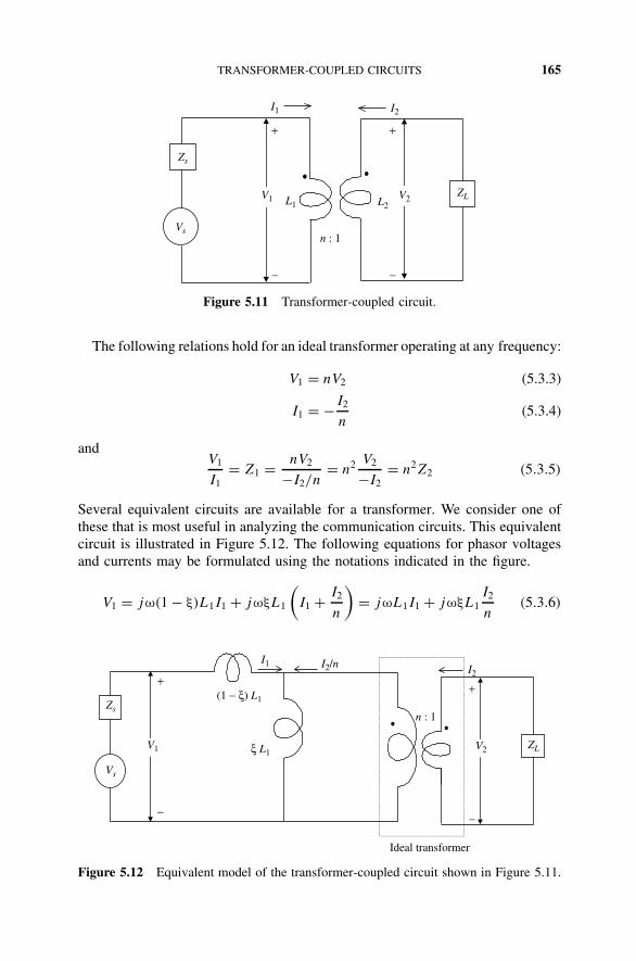
TRANSFORMER-COUPLED CIRCUITS 165
Vs
Zs
V1 L1
I1
ZLL2
I2
+
−
+
−
n : 1
V2
Figure 5.11 Transformer-coupled circuit.
The following relations hold for an ideal transformer operating at any frequency:
V1 = nV2 (5.3.3)
I1 = −I2
n(5.3.4)
andV1
I1= Z1 = nV2
−I2/n= n2 V2
−I2= n2Z2 (5.3.5)
Several equivalent circuits are available for a transformer. We consider one ofthese that is most useful in analyzing the communication circuits. This equivalentcircuit is illustrated in Figure 5.12. The following equations for phasor voltagesand currents may be formulated using the notations indicated in the figure.
V1 = jω(1 − ξ)L1I1 + jωξL1
(I1 + I2
n
)= jωL1I1 + jωξL1
I2
n(5.3.6)
Vs
Zs
V1
I1
+
−
V2 ZL
I2
+
−
(1 − ξ) L1
n : 1
I2/n
Ideal transformer
ξ L1
Figure 5.12 Equivalent model of the transformer-coupled circuit shown in Figure 5.11.

166 RESONANT CIRCUITS
and
V2 = 1
n
[jωξL1
(I1 + I2
n
)](5.3.7)
If the circuit shown in Figure 5.12 is equivalent to that shown in Figure 5.11,these two equations represent the same voltages as those of (5.3.1) and (5.3.2).Hence,
ξL1
n= M (5.3.8)
andξL1
n2= L2 (5.3.9)
In other words,
n =√
ξL1
L2(5.3.10)
and
ξ = nM
L1= M
√ξ√
L1L2⇒ √
ξ = M√L1L2
= κ (5.3.11)
where κ is called the coefficient of coupling. It is close to unity for a tightlycoupled transformer, and close to zero for a loose coupling.
Example 5.3 A tightly coupled transformer is used in the circuit shown inFigure 5.13. Inductances of its primary and secondary sides are 320 and 20 nH,respectively. Find its equivalent circuit, the resonant frequency, and the Q ofthis circuit.
V1V2
L1 L2
I1 I2
+ +
− −
62.5 kΩ30.7 pF6 pFIs
Figure 5.13 Transformer-coupled resonant circuit.

TRANSFORMER-COUPLED CIRCUITS 167
V1 C1
+
−
V2
+
−
L1R1Is
n : 1
Ideal transformer
Figure 5.14 Equivalent model of the transformer-coupled circuit shown in Figure 5.13.
SOLUTION Since the transformer is tightly coupled, κ ≈ 1. Therefore, ξ ≈1, 1 − ξ ≈ 0, and its equivalent circuit simplifies as shown in Figure 5.14. From(5.3.10),
n =√
ξL1
L2≈
√320
20= 4
and from (5.3.5),
Z1 = n2Z2 ⇒ Y1 = Y2
n2= 1
n2
(1
R2+ jωC2
)
Therefore,
R1 = n2R2 = 16 × 62.5 k = 1 M
C1 = 6 + 1
4230.7 pF = 6 + 1.91875 ≈ 7.92 pF
ω0 = 1√L1C1
= 1√320 × 10−9 × 7.92 × 10−12
= 628.1486 × 10⁶ rad/s
f0 = ω0
2π= 99.97 MHz ≈ 100 MHz
and
Q = R1
ω0L1= 106
628.1486 × 106 × 320 × 10−9= 4974.9375
Example 5.4 A transformer-coupled circuit is shown in Figure 5.15. Draw itsequivalent circuit using an ideal transformer.
(a) If the transformer is tuned only to its secondary side (i.e., R1 and C1 areremoved), determine its resonant frequency and impedance seen by the currentsource.

168 RESONANT CIRCUITS
IsV1
V2L1 L2
I1 I2
++
− −
R1
R2
C1C2
I0
Figure 5.15 Double-tuned transformer-coupled circuit.
(b) Determine the current transfer function (I0/Is) for the entire circuit (i.e.,R1 and C1 are included in the circuit). If the transformer is loosely coupled, andboth of the sides have identical quality factors as well as the resonant frequen-cies, determine the locations of the poles of the current transfer function on thecomplex ω-plane.
SOLUTION Following the preceding analysis and Figure 5.12, the equivalentcircuit can be drawn easily, as shown in Figure 5.16. Using notations as indicatedin the figure, circuit voltages and currents can be found as follows:
nV2 = sξL1
(I1 + I2
n
)(5.3.12)
V2 = −I2R2
1 + sR2C2= R2I0 (5.3.13)
Is = I1 +(
1
R1+ sC1
)[nV2 + s(1 − ξ)L1I1] (5.3.14)
R2
I0
I1
V1
+
−
V2
I2
+
−
(1 − ξ)L1
n : 1
I2/n
Ideal transformer
IsR1
C1C2nV2
+
−
ξL1
Figure 5.16 Equivalent representation for the circuit shown in Figure 5.15.

TRANSFORMER-COUPLED CIRCUITS 169
From (5.3.12), (5.3.13), and (5.3.10), we find that
(1 + s2ξL1R2C2 + sξL1
n2R2
)V2 =
(1 + s2L2C2 + sL2
R2
)R2I0 = sξL1
nI1
orI0
I1= sξL1/nR2
1 + s2L2C2 + sL2/R2(5.3.15)
When R1 and C1 are absent, I1 will be equal to Is , and (5.3.15) will representthe current transfer characteristics. This equation is similar to (5.2.2). Hence, theresonant frequency is found as follows:
ω0 = 1√L2C2
(5.3.16)
Note that the resonant frequency in this case depends only on L2 and C2. It isindependent of inductance L1 of the primary side. The impedance seen by thecurrent source, with R1 and C1 removed, is determined as follows:
Zin(s) = V1
I1= sL1(1 − ξ) + n2sL2
s2L2C2 + s(L2/R2) + 1(5.3.17)
At resonance,Zin(jω0) = jω0L1(1 − ξ) + n2R2 (5.3.18)
and if transformer is tightly coupled, ξ ≈ 1,
Zin(jω0) = n2R2 (5.3.19)
When R1 and C1 are included in the circuit, (5.3.12) to (5.3.14) can be solvedto obtain a relationship between I0 and Is . The desired current transfer functioncan be obtained as
I0
Is
= sξL1/nR2
[s2L2C2 + s(L2/R2) + 1]1 + s(1 − ξ)L1[(1/R1) + sC1]+sξL1[(1/R1) + sC1]
(5.3.20)
Note that the denominator of this equation is now a polynomial of the fourthdegree. Hence, this current ratio has four poles on the complex ω-plane. If thetransformer is loosely coupled, ξ will be negligible. In that case, the denominatorof (5.3.20) can be approximated as follows:
I0
Is
≈ sξL1/nR2
[s2L2C2 + s(L2/R2) + 1]1 + sL1[(1/R1) + sC1] + sξL1[(1/R1) + sC1](5.3.21)
170 RESONANT CIRCUITS
For ω1 = ω2 = ω0, and Q1 = Q2 = Q0,
L1C1 = L2C2 = 1
ω20
andR1
L1= R2
L2= ω0Q0
Hence, (5.3.21) may be written as
I0
Is
≈ sξL1/nR2
(s2/ω20 + s/ω0Q + 1)2 + ξ(s2/ω2
0 + s/ω0Q)(5.3.22)
The poles of (5.3.22) are determined by solving the equation
(s2
ω20
+ s
ω0Q0+ 1
)2
+ ξ
(s2
ω20
+ s
ω0Q0
)= 0 (5.3.23)
The roots of this equation are found to be
s ≈ − ω0
2Q0± jω0
√(1 ∓ √
ξ) −(
1
2Q0
)2
(5.3.24)
5.4 TRANSMISSION LINE RESONANT CIRCUITS
Transmission lines with open- or short-circuited ends are frequently used asresonant circuits in the ultrahigh frequency and microwave range. We con-sider such networks in this section. Since the quality factor is an importantparameter of these circuits, we need to include the finite (even though small)loss in the line. There are four basic types of these networks, as illustrated inFigure 5.17.
It can be found easily by analyzing the input impedance characteristics aroundthe resonant wavelength, λr , that the circuits of Figure 5.17 (a) and (d) behavelike a series R–L–C circuit. On the other hand, the other two transmission linespossess the characteristics of a parallel resonant circuit. A quantitative analysisof these circuits is presented below for n as unity.
Short-Circuited Line
Consider a transmission line of length l and characteristic impedance Z0. It hasa propagation constant, γ = α + jβ. The line is short circuited at one of its ends,as shown in Figure 5.18. The impedance at its other end, Zin, can be determined

TRANSMISSION LINE RESONANT CIRCUITS 171
4(2n − 1)λr
γ = α + jβ
γ = α + jβ
γ = α + jβ
Z0
γ = α + jβ
Z0
Open
Short
Z0 Open
Z0 Short
(a)
(c) (d )
(b)
l =
4(2n − 1)λr
2n λr
2n λr
l =
l =l =
Figure 5.17 Four basic types of transmission line resonant circuits, n = 1, 2, . . . .
Zin → γ = α + jβZ0
l
Figure 5.18 Short-circuited lossy transmission line.
from (3.2.5) as follows:
Zin = Z0 tanh γl = Z0 tanh(α + jβ)l = Z0tanh αl + j tan βl
1 + j tanh αl tan βl(5.4.1)
For αl 1, tanh αl ≈ αl, and assuming that the line supports only the TEMmode, we find that βl = ωl/vp. Hence, it can be simplified around the resonantfrequency, ω0, as follows:
βl = ωl
vp
= ω0l
vp
+ δωl
vp
= βr l + δωl
vp
(5.4.2)
where βr is the phase constant at the resonance.If the transmission line is one-half wavelength long at the resonant frequency,
βr l = π andl
vp
= π
ω0.

172 RESONANT CIRCUITS
Therefore, tan βl can be approximated as follows:
tan βl = tan
(π + δω l
vp
)= tan
(π + π δω
ω0
)= tan
π δω
ω0≈ π δω
ω0
and
Zin ≈ Z0αl + j (π δω/ω0)
1 + j (αl)(π δω/ω0)≈ Z0
(αl + j
π δω
ω0
)(5.4.3)
It is assumed in (5.4.3) that (αl)(π δω/ω0) 1.For a series resonant circuit, Zin ≈ R + j2δωL. Hence, a half-wavelength-long
transmission line with short-circuit termination is similar to a series resonant cir-cuit. The equivalent-circuit parameters are found as follows (assuming that lossesin the line are small such that the characteristic impedance is a real number):
R ≈ Z0αl = 12Z0αλr (5.4.4)
L ≈ π
2
Z0
ω0(5.4.5)
C ≈ 2
πω0Z0(5.4.6)
and
Q = ω0L
R≈ π
2αl= βr
2α(5.4.7)
On the other hand, if the transmission line is a quarter-wavelength long at theresonant frequency, βr l = π/2, and l/vp = π/2 ω0. Therefore,
tan βl = tan
(π
2+ δωl
vp
)= tan
(π
2+ πδω
2 ω0
)= − cot
(πδω
2 ω0
)≈ −2 ω0
πδω(5.4.8)
and
Zin ≈ Z0−j (2 ω0/πδω)
1 − jαl(2 ω0/πδω)= Z0/αl
1 + j (π/αl)(δω/2 ω0)(5.4.9)
This expression is similar to the one obtained for a parallel resonant circuitin (5.2.9). Therefore, this transmission line is working as a parallel resonantcircuit with equivalent parameters as follows:
Rp ≈ Z0
αl= 4Z0
αλr
(5.4.10)
Lp ≈ 4Z0
πω0(5.4.11)
Cp ≈ π
4 ω0Z0(5.4.12)

TRANSMISSION LINE RESONANT CIRCUITS 173
and
Q = π
4αl= βr
2α(5.4.13)
Open-Circuited Line
The analysis of the open-circuited transmission line shown in Figure 5.19 can beperformed following a similar procedure. These results are summarized below.From (3.2.5),
Zin|ZL=∞ = Z0
tanh γl(5.4.14)
For a transmission line that is a half-wavelength long, the input impedance canbe approximated as follows:
Zin ≈ Z01 + j (αl)(πδω/ω0)
αl + j (πδω/ω0)≈ Z0
αl + j (πδω/ω0)(5.4.15)
This is similar to (5.2.9). Therefore, a half-wavelength-long open-circuited trans-mission line is similar to a parallel resonant circuit with equivalent parametersas follows:
Rp ≈ Z0
αl= 2Z0
αλr
(5.4.16)
Lp ≈ 2Z0
πω0(5.4.17)
Cp ≈ π
2 ω0Z0(5.4.18)
and
Q = π
2αl= βr
2α(5.4.19)
If the line is only a quarter-wavelength long, the input impedance can be approx-imated as
Zin ≈ Z01 − j (αl)(2 ω0/πδω)
αl − j (2 ω0/πδω)≈ Z0
(αl + j
πδω
2 ω0
)(5.4.20)
Zin → γ = α + jβZ0
l
Figure 5.19 Open-circuited transmission line.

174 RESONANT CIRCUITS
TABLE 5.2 Equivalent-Circuit Parameters of the Resonant Lines for n = 1
Quarter-wavelength line Half-wavelength line
Open Circuit Short Circuit Open Circuit Short Circuit
Resonance Series Parallel Parallel Series
R 14 Z0αλr
4Z0
αλr
2Z0
αλr
12Z0αλr
LπZ0
4 ω0
4Z0
πω0
2Z0
πω0
πZ0
2 ω0
C4
πZ0ω0
π
4Z0ω0
π
2Z0ω0
2
πZ0ω0
Qβr
2α
βr
2α
βr
2α
βr
2α
Since (5.4.20) is similar to (5.1.17), this transmission line works as a series reso-nant circuit. Its equivalent-circuit parameters are found as follows (see Table 5.2):
R ≈ Z0αl = 14Z0αλr (5.4.21)
L ≈ πZ0
4 ω0(5.4.22)
C ≈ 4
πω0Z0(5.4.23)
and
Q = πZ0
4R= π
4αl= β0
2α(5.4.24)
Example 5.5 Design a half-wavelength-long coaxial line resonator that is short-circuited at its ends. Its inner conductor radius is 0.455 mm and the inner radiusof the outer conductor is 1.499 mm. The conductors are made of copper. Com-pare the Q value of an air-filled resonator to that of a Teflon-filled resonatoroperating at 5 GHz. The dielectric constant of Teflon is 2.08 and its loss tangentis 0.0004.
SOLUTION From the relations for coaxial lines given in Appendix 2,
Rs =√
ωµ0
2σ=
√2π × 5 × 109 × 4π × 10−7
2 × 5.813 × 107= 0.018427
αc = Rs
2 ln(b/a)√
µ0/ε0
(1
a+ 1
b
)

TRANSMISSION LINE RESONANT CIRCUITS 175
= 0.018427
2 × 376.7343 × ln(1.499/0.455)
(100
0.455+ 100
1.499
)= 0.058768 Np/m
With Teflon filling,
αc = Rs
2√
µ0/ε0εr ln(b/a)
(1
a+ 1
b
)
= 0.018427 × √2.08
2 × 376.7343 × ln(1.499/0.455)
(100
0.455+ 100
1.499
)= 0.084757 Np/m
αd = ω
2
√µ0ε0εr tan δ = π × 5 × 109 × 3 × 108 × √
2.08 × 0.0004
= 0.030206 Np/m
β0 = 2π × 5 × 109
3 × 108= 104.719755 rad/m
βd = 2π × 5 × 109 × √2.08
3 × 108= 151.029 rad/m
Qair = β0
2α= 104.719755
2 × 0.058768= 890.96
QTeflon = βd
2α= 151.029
2 × (0.084757 + 0.030206)= 656.8629
Example 5.6 Design a half-wavelength-long microstrip resonator using a 50-line that is short circuited at its ends. The substrate thickness is 0.159 cm, withits dielectric constant 2.08 and the loss tangent 0.0004. The conductors are madeof copper. Compute the length of the line for resonance at 2 GHz and the Q ofthe resonator. Assume that thickness t of the microstrip is 0.159 µm.
SOLUTION Design equations for the microstrip line (from Appendix 2) are
w
h=
8eA
e2A − 2for A > 1.52
2
π
B − 1 − ln(2B − 1) + εr − 1
2εr
×[
ln(B − 1) + 0.39 − 0.61
εr
] for A ≤ 1.52
where
A = Z0
60
(εr + 1
2
)1/2
+ εr − 1
εr + 1
(0.23 + 0.11
εr
)
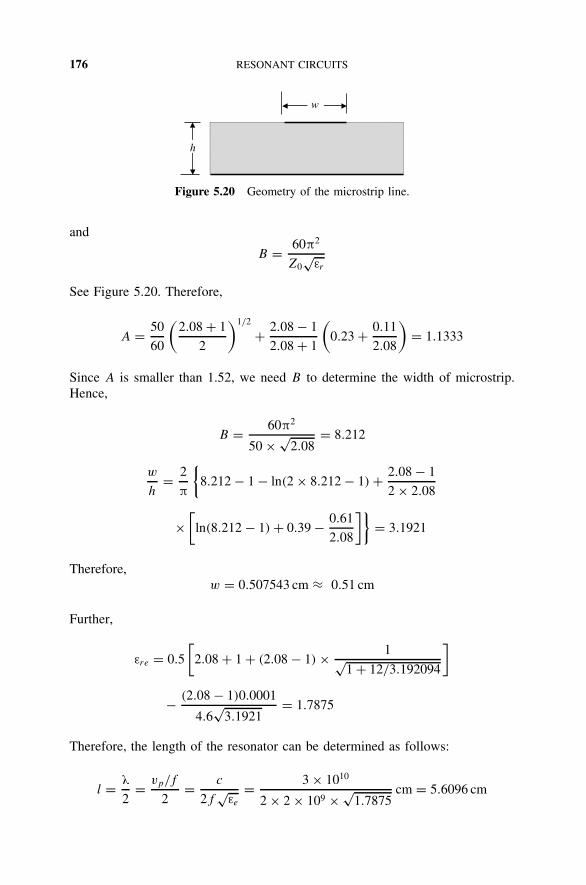
176 RESONANT CIRCUITS
w
h
Figure 5.20 Geometry of the microstrip line.
and
B = 60π2
Z0√
εr
See Figure 5.20. Therefore,
A = 50
60
(2.08 + 1
2
)1/2
+ 2.08 − 1
2.08 + 1
(0.23 + 0.11
2.08
)= 1.1333
Since A is smaller than 1.52, we need B to determine the width of microstrip.Hence,
B = 60π2
50 × √2.08
= 8.212
w
h= 2
π
8.212 − 1 − ln(2 × 8.212 − 1) + 2.08 − 1
2 × 2.08
×[
ln(8.212 − 1) + 0.39 − 0.61
2.08
]= 3.1921
Therefore,w = 0.507543 cm ≈ 0.51 cm
Further,
εre = 0.5
[2.08 + 1 + (2.08 − 1) × 1√
1 + 12/3.192094
]
− (2.08 − 1)0.0001
4.6√
3.1921= 1.7875
Therefore, the length of the resonator can be determined as follows:
l = λ
2= vp/f
2= c
2f√
εe
= 3 × 10¹⁰
2 × 2 × 109 × √1.7875
cm = 5.6096 cm

MICROWAVE RESONATORS 177
Since σcopper = 5.813 × 10⁷ S/m, the quality factor of this resonator is determinedas follows. For w/h ≥ 1/2π,
we
h= w
h+ 0.3979
t
h
[1 + ln
(2h
t
)]= 3.1923
and
ζ = 1 + h
we
[1 − 1.25t
πh+ 1.25
πln
(2h
t
)]= 2.5476
Therefore, for w/h ≥ 1, αc is found to be
αc = 44.1255 × 10⁻⁵ ζZ0εre
h
√fGHz
σ
[we
h+ 0.667 (we/h)
we/h + 1.444
]Np/m
= 0.0428 Np/m
Similarly, αd is found from (A2.28) as follows:
αd = 10.4766εr
εr − 1
εre − 1√εre
fGHz tan δ Np/m = 0.0095 Np/m
and
β = 2π
λ= 2π
2l= 2π
2 × 5.6096/100rad/m = 56.0035 rad/m
Hence, Q of the resonator is found as
Q = β
2α= 56.0035
2 × (0.0428 + 0.0095)= 535.4
5.5 MICROWAVE RESONATORS
Cavities and dielectric resonators are commonly employed as resonant circuitsat frequencies above 1 GHz. These resonators provide much higher Q than thelumped elements and transmission line circuits. However, the characterization ofthese devices requires analysis of associated electromagnetic fields. Character-istic relations of selected microwave resonators are summarized in this section.Interested readers can find several excellent references and textbooks analyzingthese and other resonators.
Rectangular Cavities
Consider a rectangular cavity made of conducting walls with dimensions a ×b × c, as shown in Figure 5.21. It is filled with a dielectric material of dielectricconstant εr and relative permeability µr . In general, it can support both TEmnp

178 RESONANT CIRCUITS
a
b
c
x
y
z
Figure 5.21 Geometry of the rectangular cavity resonator.
and TMmnp modes, which may be degenerate. The cutoff frequency of TEmn andTMmn modes can be determined from the formula
fc(MHz) = 300√µrεr
√[( m
2a
)2 +( n
2b
)2]
MHz
The resonant frequency fr of a rectangular cavity operating in either TEmnp orTMmnp mode can be determined as follows:
fr(MHz) = 300√µrεr
√[( m
2a
)2 +( n
2b
)2 +( p
2c
)2]
MHz (5.5.1)
If the cavity is made of a perfect conductor and filled with a perfect dielectric,it will have infinite Q. However, it is not possible in practice. In the case of cavitywalls having a finite conductivity (instead of infinite for the perfect conductor)but filled with a perfect dielectric (no dielectric loss), its quality factor Qc forTE10p mode is given by
Qc|10p = 60b(acω√
µε)3
πRs(2p2a3b + 2bc3 + p2a3c + ac3)
õr
εr
(5.5.2)
The permittivity and permeability of the dielectric filling are given by ε and µ,respectively, ω is angular frequency, and Rs is the surface resistivity of walls,which is related to the skin depth δs and the conductivity σ as follows.
Rs = 1
σδs
=√
ωµ
2σ(5.5.3)
On the other hand, if the cavity is filled with a dielectric with its loss tangentas tan δ while its walls are made of a perfect conductor, the quality factor Qd isgiven as
Qd = 1
tan δ(5.5.4)

MICROWAVE RESONATORS 179
When there is power loss in both the cavity walls and the dielectric filling, thequality factor Q is found from Qc and Qd as follows:
1
Q= 1
Qc
+ 1
Qd
(5.5.5)
Example 5.7 An air-filled rectangular cavity is made from a piece of copperWR-90 waveguide. If it resonates at 9.379 GHz in TE101 mode, find the requiredlength c and the Q value of this resonator.
SOLUTION Specifications of WR-90 are given in Table A3.3 as follows:
a = 0.9 in. = 2.286 cm
and
b = 0.4 in. = 1.016 cm
From (5.5.1),
1
2c=
√(9379
300
)2
−(
1
2a
)2
= 22.3383 ⇒ c = 2.238 cm
Next, the surface resistance, Rs , is determined from (5.5.3) as 0.0253 , and theQc is found from (5.5.2) to be about 7858.
Example 5.8 A rectangular cavity made of copper has inner dimensions a =1.6 cm, b = 0.71 cm, and c = 1.56 cm. It is filled with Teflon (εr = 2.05 andtan δ = 2.9268 × 10⁻⁴). Find the TE101 mode resonant frequency and Q valueof this cavity.
SOLUTION From (5.5.1),
fr = 300√2.05
√(1
2 × 0.016
)2
+(
1
2 × 0.0156
)2
≈ 9379 MHz = 9.379 GHz
Since power dissipates both in the dielectric filling as well as in the sidewalls,overall Q will be determined from (5.5.5). From (5.5.2) and (5.5.4), Qc and Qd
are found to be 5489 and 3417, respectively. Substituting these into (5.5.5), theQ value of this cavity is found to be 2106.
Circular Cylindrical Cavities
Figure 5.22 shows the geometry of a circular cylindrical cavity of radius r andheight h. It is filled with a dielectric material of relative permeability µr and

180 RESONANT CIRCUITS
r
h
x
y
z
Figure 5.22 Geometry of the circular cylindrical cavity resonator.
dielectric constant εr . Its resonant frequency fr in megahertz is given as
fr(MHz) = 300
2π√
µrεr
√(χnm
r
)2 +(pπ
h
)2MHz (5.5.6)
where
χnm =pnm for TM modesp′
nm for TE modes (5.5.7)
As discussed in Section 4.9, pnm represents the mth zero of the Bessel functionof the first kind and order n and p′
nm represents the mth zero of the derivativeof the Bessel function. In other words, these represent roots of the followingequations, respectively (see Table 5.3):
Jn(x) = 0 (5.5.8)
anddJn(x)
dx= 0 (5.5.9)
The Qc of a circular cylindrical cavity operating in TEnmp mode and filledwith a lossless dielectric can be found from the following formula:
Qc = 47.7465
δsfr (MHz)
[1 − (
n/p′nm
)2] [
(p′nm)2 + (pπr/h)2
]1.5
[p
′2nm + (2r/h) (pπr/h)2
] +[1 − (2r/h)
(npπr/p
′nmh
)2]
(5.5.10)
TABLE 5.3 Zeros of Jn(x) and J′n(x)
n pn1 pn2 pn3 p′n1 p
′n2 p
′n3
0 2.405 5.520 8.654 3.832 7.016 10.1731 3.832 7.016 10.173 1.841 5.331 8.5362 5.136 8.417 11.620 3.054 6.706 9.969

MICROWAVE RESONATORS 181
In the case of TMnmp mode, Qc is given by
Qc = 47.7465
δsfr (MHz)
√[p2
nm + (pπr/h)2]
1 + (2r/h)p > 0 (5.5.11)
For p = 0,
Qc ≈ 47.7465
δsfr (MHz)
pnm
1 + (r/h)p = 0 (5.5.12)
The quality factor Qd due to dielectric loss and the overall Q are determined asbefore from (5.5.4) and (5.5.5) with appropriate Qc.
Example 5.9 Determine the dimensions of an air-filled circular cylindrical cav-ity that resonates at 5 GHz in TE011 mode. It should be made of copper, and itsheight should be equal to its diameter. Find the Q of this cavity given that n = 0,m = p = 1, and h = 2r .
SOLUTION From (5.5.6), with χ01 as 3.832 from Table 5.3, we get
r =√
3.8322 + (π/2)2
(5000 × 2π/300)2= 0.03955 m
and
h = 2r = 0.0791 m
Since
δs =√
2
ωµσ=
√2
2π × 5 × 109 × 4π × 10−7 × 5.8 × 107= 9.3459 × 10⁻⁷ m
The Q value of the cavity can be found from (5.5.10) as
Qc = 47.7465 × 10⁶
9.3459 × 10−7 × 5 × 109× [3.8322 + (π/2)2]1.5
[3.8322 + (π/2)2] + 1= 39, 984.6
Further, there is no loss of power in air (tan δ ≈ 0), Qd is infinite, and thereforeQ is the same as Qc.
Dielectric Resonators
Dielectric resonators (DRs), made of high-permittivity ceramics, provide highQ values with smaller size. These resonators are generally a solid sphere orcylinder of circular or rectangular cross section. High-purity TiO2 (εr ≈ 100,tan δ ≈ 0.0001) was used in early dielectric resonators. However, it was found

182 RESONANT CIRCUITS
h
2r
Figure 5.23 Geometry of an isolated circular cylindrical dielectric resonator.
to be intolerably dependent on the temperature. With the development of newceramics, temperature dependence of DR can be reduced significantly.
Figure 5.23 shows an isolated circular cylindrical DR. Its analysis is beyondthe scope of this book. Its TE01δ -mode resonant frequency, fr in GHz, can befound from the following formula:
fr(GHz) = 34
rεr
(3.45 + r
h
)GHz (5.5.13)
where r and h are in millimeters. This relation is found to be accurate within±2% if
2 >r
h> 0.5 (5.5.14)
and
50 > εr > 30 (5.5.15)
An isolated DR is of almost no use in practice. A more practical situationis illustrated in Figure 5.24, where it is coupled with a microstrip line in aconducting enclosure. Assume that the dielectric constants of the DR and thesubstrate are εr and εs , respectively. With various dimensions as shown (all inmeters), the following formulas can be used to determine its radius r and theheight h. If r is selected between the following bounds, the formulas presentedin this section are found to have a tolerance of no more than 2% (Kajfez andGuillon, 1986):
1.2892 × 10⁸
fr
√εs
> r >1.2892 × 10⁸
fr
√εr
(5.5.16)
where fr is resonant frequency in hertz.The height of the DR is then found as
h = 1
β
(tan−1 α1
β tanh α1t+ tan−1 α2
β tanh α2d
)(5.5.17)

MICROWAVE RESONATORS 183
where
α1 =√
k′2 − k2
0εs (5.5.18)
α2 =√
k′2 − k2
0 (5.5.19)
β =√
k20εr − k
′2 (5.5.20)
k′ = 2.405
r+ y
2.405r[1 + (2.43/y) + 0.291y](5.5.21)
y =√
(k0r)2(εr − 1) − 5.784 (5.5.22)
and
k0 = ω√
µ0ε0 (5.5.23)
Example 5.10 Design a TE01δ-mode cylindrical dielectric resonator for use at35 GHz in the microstrip circuit shown in Figure 5.24. The substrate is 0.25 mmthick and its dielectric constant is 9.9. The dielectric constant of the materialavailable for DR is 36. Further, the top of the DR should have a clearance of1 mm from the conducting enclosure.
SOLUTION Since
1.2892 × 10⁸
fr
√εs
= 1.171 × 10⁻³ m
and
1.2892 × 10⁸
fr
√εr
= 6.139 × 10⁻⁴ m
the radius r of the DR may be selected as 0.835 mm.
d
h
t Substrate
Conductingenclosure
DR Microstrip
2r
Figure 5.24 Geometry of a circular cylindrical dielectric resonator in MIC configuration.

184 RESONANT CIRCUITS
The height h of the DR is then determined from (5.5.17) to (5.5.22), as follows:
y =√
(k0r)2(εr − 1) − 5.784 = 2.707
k′ = 2.405
r+ y
2.405r[1 + (2.43/y) + 0.291y]= 3.382 × 10³
α1 =√
k′2 − k2
0εs = 2.474 × 10³
α2 =√
k′2 − k2
0 = 3.302 × 10³
andβ =
√k2
0εr − k′2 = 2.812 × 10³
After substituting these numbers into (4.5.17), h is found to be
h = 1
β
(tan−1 α1
β tanh α1t+ tan−1 α2
β tanh α2d
)= 6.683 × 10⁻⁴ m = 0.668 mm
SUGGESTED READING
Bahl, I., and P. Bhartia, Microwave Solid State Circuit Design. New York: Wiley, 1988.Collin, R. E., Foundations for Microwave Engineering. New York: McGraw-Hill, 1992.Elliott, R. S., An Introduction to Guided Waves and Microwave Circuits. Englewood Cliffs,
NJ: Prentice Hall, 1993.Kajfez, D., and P. Guillon, Dielectric Resonators. Dedham, MA: Artech House, 1986.Pozar, D. M., Microwave Engineering. New York: Wiley, 1998.
Ramo, S., J. R. Whinnery, and T. Van Duzer, Fields and Waves in Communication Elec-tronics. New York: Wiley, 1994.
Rizzi, P.A., Microwave Engineering. Englewood Cliffs, NJ: Prentice Hall, 1988.Smith, J. R., Modern Communication Circuits. New York: McGraw-Hill, 1998.
PROBLEMS
5.1. Determine the resonant frequency, bandwidth, and Q of the circuit shownin Figure P5.1.
2 nH 0.015 µF
50 Ωvin(t) vo(t)
Figure P5.1

PROBLEMS 185
5.2. The quality factor of a 100-nH inductor is 150 at 100 MHz. It is used in aseries resonant circuit with a 50- load resistor. Find the capacitor requiredto resonate this circuit at 100 MHz. Find the loaded Q value of the circuit.
5.3. Find the capacitance C in the series R–L–C circuit shown in Figure P5.3if it is resonating at 1200 rad/s. Compute the output voltage vo(t) whenvin(t) = 4 cos(ωt + 0.2π) V for ω as 1200, 300, and 4800 rad/s.
10 mH C
2 Ωvin(t) vo(t)
Figure P5.3
5.4. The magnitude of input impedance in the series R–L–C circuit shown inFigure P5.4 is found to be 3 at a resonant frequency of 1600 rad/s. Findthe inductance L, Q, and the bandwidth.
L 20 µF
Rvin(t) vo(t)
Figure P5.4
5.5. Determine the element values of a resonant circuit to filter all the sinusoidalsignals from 100 to 130 MHz. This filter is to be connected between avoltage source with negligible internal impedance and a communicationsystem that has an input impedance of 50 . Plot its response over thefrequency range 50 to 200 MHz.
5.6. A series resonant circuit is resonating at 105 rad/s and has a bandwidth of100 rad/s. If the resistance in the circuit is 50 , find its inductance andcapacitance.
5.7. For the circuit given in Figure P5.7, the poles are located as illustrated inFigure P7.2. Find (a) the Q, (b) ω0, (c) ω, (d) ω1, and (e) ω2.

186 RESONANT CIRCUITS
−σ
(a) (b)
L C
50 Ωvin(t) vo(t)
jω
98,000
−98,000
−2 × 10⁴
Figure P5.7 (a) Series R–L–C circuit with input–output terminals; (b) poles of thetransfer function.
5.8. Calculate the resonant frequency, Q, and bandwidth of the parallel resonantcircuit shown in Figure P5.8.
2 nH0.015 µF 100 kΩ
Figure P5.8
5.9. Find the resonant frequency, unloaded Q, and loaded Q of the parallelresonant circuit shown in Figure P5.9.
20 nH 50 pF500 Ω
1 kΩ
Resonator circuit Load
Figure P5.9
5.10. The parallelR–L–C circuit shown in Figure P5.10 is resonant at 20,000 rad/s.If its admittance has a magnitude of 1 mS at the resonance, find the values ofR and L.

PROBLEMS 187
L0.05 µF R
Figure P5.10
5.11. Consider the loaded parallel resonant circuit shown in Figure P5.11. Com-pute the resonant frequency in radians per second, unloaded Q, and loadedQ of this circuit.
2 kΩ
20 mH50 µF
10 kΩ
Load
Figure P5.11
5.12. Resistance R in a parallel R–L–C circuit is 200 . The circuit has abandwidth of 80 rad/s with a lower half-power frequency at 800 rad/s. Findthe inductance and capacitance of the circuit.
5.13. A parallel R–L–C circuit is resonant at 2 × 10⁶ rad/s and has a band-width of 20,000 rad/s. If its impedance at resonance is 2000 , find thecircuit parameters.
5.14. A resonator is fabricated from a 2λ-long transmission line that is short-circuited at its ends. Find its Q.
5.15. A 3-cm-long 100- air-filled coaxial line is used to fabricate a resonator.It is short-circuited at one end while a capacitor is connected at the otherend to obtain the resonance at 6 GHz. Find the value of this capacitor.
5.16. A 100- air-filled coaxial line of length l is used to fabricate a resonator. Itis terminated by 10 −j5000 at its ends. If the signal wavelength is 1 m,find the required length for the first resonance and the Q of this resonator.
5.17. Design a half-wavelength-long coaxial line resonator that is short-circuitedat its ends. Its inner conductor radius is 0.455 mm and the inner radiusof the outer conductor is 1.499 mm. The conductors are made of copper.Compare the Q value of an air-filled resonator to that of a Teflon-filledresonator operating at 800 MHz. The dielectric constant of Teflon is 2.08and its loss tangent is 0.0004.
5.18. Design a half-wavelength-long microstrip resonator using a 50- line thatis short-circuited at its ends. The substrate thickness is 0.12 cm with a

188 RESONANT CIRCUITS
dielectric constant of 2.08 and a loss tangent of 0.0004. The conductorsare of copper. Compute the length of the line for resonance at 900 MHzand the Q value of the resonator.
5.19. The secondary side of a tightly coupled transformer is terminated by a2-k load in parallel with capacitor C2. A current source I = 10 cos(4 ×10⁶) mA is connected on its primary side. The inductance L1 of its primaryis 0.30 µH, the mutual inductance M = 3 µH, and the unloaded Q of thesecondary coil is 70. Determine the value of C2 such that this circuitresonates at 4 × 10⁶ rad/s. Find its input impedance and the output voltageat the resonant frequency. What is the circuit bandwidth?
5.20. A 16- resistor terminates the secondary side of a tightly coupled trans-former. A 40-µF capacitor is connected in series with its primary coil,which has an inductance L1 at 100 mH. If the secondary coil has aninductance L2 at 400 mH, find the resonant frequency and the Q valueof the circuit.
5.21. A 16- resistor terminates the secondary side of a tightly coupled trans-former. A 30-µF capacitor is connected in series with its primary coil,which has an inductance of 25 mH. If the circuit Q value is 50, find theinductance L2 of the secondary coil.
5.22. An air-filled rectangular cavity is made from a piece of copper WR-430waveguide. If it resonates at 2 GHz in TE101 mode, find the required lengthc and the Q of this resonator.
5.23. Design an air-filled circular cylindrical cavity that resonates at 9 GHz inTE011 mode. It should be made of copper, and its height should be equalto its diameter. Find the Q value of this cavity.
5.24. Design a TE01δ mode cylindrical dielectric resonator for use at 4.267 GHz inthe microstrip circuit shown in Figure 5.24. The substrate is 0.7 mm thickand its dielectric constant is 9.6. The dielectric constant of the materialavailable for the DR is 34.19. Further, the top of the DR should have aclearance of 0.72 mm from the conducting enclosure.

6IMPEDANCE-MATCHING NETWORKS
One of the most critical requirements in the design of high-frequency electroniccircuits is that the maximum possible signal energy is transferred at each point. Inother words, the signal should propagate in a forward direction with a negligibleecho (ideally, zero). Echo signal not only reduces the power available but alsodeteriorates the signal quality due to the presence of multiple reflections. Asnoted in Chapter 5, impedance can be transformed to a new value by adjustingthe turns ratio of a transformer that couples it with the circuit. However, it hasseveral limitations. In this chapter we present a few techniques to design otherimpedance-transforming networks. These circuits include transmission line stubsand resistive and reactive networks. Further, the techniques introduced are neededin active circuit design at RF and microwave frequencies.
As shown in Figure 6.1, impedance-matching networks are employed at theinput and output of an amplifier circuit. These networks may also be neededto perform other tasks, such as filtering the signal and blocking or passing thedc bias voltages. This chapter begins with a section on impedance-matchingtechniques that use a single reactive element or stub connected in series or inshunt. Theoretical principles behind the technique are explained, and the graphicalprocedure to design these circuits using a Smith chart is presented. Principles andprocedures of double-stub matching are discussed in the following section. Thechapter ends with sections on resistive and reactive L-section matching networks.Both analytical and graphical procedures to design these networks using ZY -charts are included.
Radio-Frequency and Microwave Communication Circuits: Analysis and Design, Second Edition,By Devendra K. MisraISBN 0-471-47873-3 Copyright 2004 John Wiley & Sons, Inc.
189

190 IMPEDANCE-MATCHING NETWORKS
Impedance-transforming
circuit
Impedance-transforming
circuit
Transistorwith dc bias
circuit
LoadZL
Vs
Zs
Figure 6.1 Block diagram of an amplifier circuit.
6.1 SINGLE REACTIVE ELEMENT OR STUB MATCHINGNETWORKS
When a lossless transmission line is terminated by an impedance ZL, the magni-tude of the reflection coefficient (and hence, the VSWR) on it remains constant,but its phase angle can be anywhere between +180 and −180. As we have seenin Chapter 3, it represents a circle on a Smith chart, and a point on this circlerepresents the normalized load. As one moves away from the load, the impedance(or the admittance) value changes. This movement is clockwise on the VSWRcircle. The real part of the normalized impedance (or normalized admittance)becomes unity at certain points on the line. Addition of a single reactive elementor a transmission line stub at this point can eliminate the echo signal and reducethe VSWR to unity beyond this point. A finite-length transmission line with itsother end an open or short circuit is called a stub and behaves like a reactiveelement, as explained in Chapter 3.
In this section we discuss the procedure for determining the location on a loss-less feeding line where a stub or a reactive element can be connected to eliminatethe echo signal. Two different possibilities, a series or a shunt element, are con-sidered. Mathematical equations as well as graphical methods are presented todesign the circuits.
Shunt Stub or Reactive Element
Consider a lossless transmission line of characteristic impedance Z0 that isterminated by a load admittance YL, as shown in Figure 6.2. Correspondingnormalized input admittance at a point ds away from the load can be foundfrom (3.2.6) as
Y in = Y L + j tan βds
1 + jYL tan βds
(6.1.1)
To obtain a matched condition at ds , the real part of the input admittance mustbe equal to the characteristic admittance of the line [i.e., the real part of (6.1.1)must be unity]. This requirement is used to determine ds . The parallel sus-ceptance Bs is then connected at ds to cancel out the imaginary part of Yin.

SINGLE REACTIVE ELEMENT OR STUB MATCHING NETWORKS 191
ds
YL = GL + jBLjBs
Figure 6.2 Transmission line with a shunt matching element.
Hence,
ds = 1
βtan−1
BL ±√
B2L − A(1 − GL)
A(6.1.2)
where A = GL(GL − 1) + B2L.
The imaginary part of the normalized input admittance at ds is found as follows:
B in = (BL + tan βds)(1 − BL tan βds) − G2L tan βds
(GL tan βds)2 + (1 − BL tan βds)2(6.1.3)
The other requirement to obtain a matched condition is
Bs = −B in (6.1.4)
Hence, a shunt inductor is needed at ds if the input admittance is found capacitive(i.e., Bin is positive). On the other hand, it will require a capacitor if Yin isinductive at ds . As mentioned earlier, a lossless transmission line section canbe used in place of this inductor or capacitor. The length of this transmissionline section is determined according to the susceptance needed by (6.1.4) andthe termination (i.e., an open circuit or a short circuit) at its other end. Thistransmission line section is called a stub. If ls is the stub length that has a shortcircuit at its other end,
ls = 1
βcot−1(−Bs) = 1
βcot−1 B in (6.1.5)
On the other hand, if there is an open circuit at the other end of the stub,
ls = 1
βtan−1 Bs = 1
βtan−1(−B in) (6.1.6)
Series Stub or Reactive Element
If a reactive element (or stub) needs to be connected in series as shown inFigure 6.3, the design procedure can be developed as follows. The normalized

192 IMPEDANCE-MATCHING NETWORKS
ds
ZL = RL + jXL
jXs
Figure 6.3 Transmission line with a matching element connected in series.
input impedance at ds is
Zin = ZL + j tan βds
1 + jZL tan βds
(6.1.7)
To obtain a matched condition at ds , the real part of the input impedance mustbe equal to the characteristic impedance of the line [i.e., the real part of (6.1.7)must be unity]. This condition is used to determine ds . A reactance Xs is thenconnected in series at ds to cancel out the imaginary part of Zin. Hence,
ds = 1
βtan−1
XL ±√
X2L − Az(1 − RL)
Az
(6.1.8)
where Az = RL(RL − 1) + X2L.
The imaginary part of the normalized input impedance at ds is found as follows:
Xin = (XL + tan βds)(1 − XL tan βds) − R2L tan βds
(RL tan βds)2 + (1 − XL tan βds)2(6.1.9)
To obtain a matched condition at ds , the reactive part Xin must be eliminated byadding an element of opposite nature. Hence,
Xs = −Xin (6.1.10)
Therefore, a capacitor will be needed in series if the input impedance is inductive.It will require an inductor if the input reactance is capacitive. As before, a trans-mission line stub can be used instead of an inductor or a capacitor. The lengthof this stub with an open circuit at its other end can be determined as follows:
ls = 1
βcot(−Xs) = 1
βcot Xin (6.1.11)

SINGLE REACTIVE ELEMENT OR STUB MATCHING NETWORKS 193
However, if the stub has a short circuit at its other end, its length will be aquarter-wavelength shorter (or longer, if the resulting number becomes negative)than this value. It can be found as
ls = 1
βtan Xs = 1
βtan(−Xin) (6.1.12)
Note that the location ds and the stub length ls are periodic in nature in both cases.It means that the matching conditions will also be satisfied at points one-halfwavelength apart. However, the shortest possible values of ds and ls are preferredbecause those provide the matched condition over a broader frequency band.
Graphical Method
These matching networks can also be designed graphically using a Smith chart.The procedure is similar for both series- and shunt-connected elements, exceptthat the former is based on the normalized impedance, whereas the latter workswith normalized admittance. It can be summarized in the following steps:
1. Determine the normalized impedance of the load and locate that point ona Smith chart.
2. Draw the constant-VSWR circle. If the stub needs to be connected inparallel, move a quarter-wavelength away from the load impedance point.This point is located at the other end of the diameter that connects the loadpoint with the center of the circle. For a series stub, stay at the normalizedimpedance point.
3. From the point found in step 2, move toward the generator (i.e., clockwise)on the VSWR circle until it intersects the unity resistance (or conductance)circle. The distance traveled to this intersection point from the load isequal to ds . There will be at least two such points within one-half wave-length from the load. A matching element can be placed at either one ofthese points.
4. If the admittance in step 3 is 1 + jB, a susceptance of −jB in shunt isneeded for matching. This can be a discrete reactive element (inductoror capacitor, depending on a negative or positive susceptance value) or atransmission line stub.
5. In the case of a stub, the length required is determined as follows. Since itsother end will have an open or a short, the VSWR on it will be infinite. It isrepresented by the outermost circle of the Smith chart. Locate the desiredsusceptance point (i.e., 0 − jB) on this circle and then move toward load(counterclockwise) until an open circuit (i.e., a zero susceptance) or a shortcircuit (an infinite susceptance) is found. This distance is equal to the stublength ls .
For a series reactive element or stub, steps 4 and 5 will be the same exceptthat the normalized reactance replaces the normalized susceptance.

194 IMPEDANCE-MATCHING NETWORKS
Example 6.1 A uniform, lossless 100- line is connected to a load of50 − j75 , as illustrated in Figure 6.4. A single stub of 100- characteristicimpedance is connected in parallel at a distance ds from the load. Find theshortest values of ds and stub length ls for a match.
SOLUTION As mentioned in the preceding analysis, design equations (6.1.2),(6.1.3), (6.1.5), and (6.1.6) for a shunt stub use admittance parameters. On theother hand, the series-connected stub design uses impedance parameters in (6.1.8),(6.1.9), (6.1.11), and (6.1.12). Therefore, ds and ls can be determined theoretically,as follows:
YL = YL
Y0= Z0
ZL
= 100
50 − j75= 0.6154 + j0.9231
A = GL(GL − 1) + B2L = 0.6154(0.6154 − 1) + 0.92312 = 0.6154
From (6.1.2), the two possible values of ds are
ds = λ
2πtan−1 −0.75 + √
(−0.75)2 − 0.6154(1 − 0.5)
0.6154= 0.1949λ
and
ds = λ
2πtan−1 −0.75 − √
(−0.75)2 − 0.6154(1 − 0.5)
0.6154= 0.0353λ
At 0.1949λ from the load, the real part of the normalized admittance is unity andits imaginary part is −1.2748. Hence, the stub should provide j1.2748 to cancelit out. Length of a short-circuited stub, ls , is calculated from (6.1.5) as
ls = 1
βcot−1(−1.2748) = 0.3941λ
ds
ZL = 50 − j75 Ω
ls
Figure 6.4 Shunt stub matching network.

SINGLE REACTIVE ELEMENT OR STUB MATCHING NETWORKS 195
On the other hand, normalized admittance is 1 + j1.2748 at 0.0353λ from theload. To obtain a matched condition, the stub at this point must provide a nor-malized susceptance of −j1.2748. Hence,
ls = 1
βcot−1(1.2748) = 0.1059λ
Thus, there are two possible solutions to this problem. In one case, a short-circuited 0.3941λ-long stub is needed at 0.1949λ from the load. The other designrequires a 0.1059λ-long short-circuited stub at 0.0353λ from the load. It is pre-ferred over the former design because of its shorter lengths.
The following steps are needed to solve this example graphically with a Smithchart:
1. Determine the normalized load admittance.
ZL = 50 − j75
100= 0.5 − j0.75
2. Locate the normalized load impedance point on the Smith chart. Draw theVSWR circle as shown in Figure 6.5.
3. From the load impedance point, move to the diametrically opposite pointand locate the corresponding normalized load admittance. It is the point0.62 + j0.91 on the chart.
4. Locate the point on the VSWR circle where the real part of the admittanceis unity. There are two such points with normalized admittance values1 + j1.3 (say, point A) and 1 − j1.3 (say, point B), respectively.
5. The distance ds of 1 + j1.3 (point A) from the load admittance can bedetermined as 0.036λ (i.e., 0.170λ − 0.134λ) and for point B (1 − j1.3)as 0.195λ (i.e., 0.329λ − 0.134λ).
6. If a susceptance of −j1.3 is added at point A or j1.3 at point B, the loadwill be matched.
7. Locate the point −j1.3 along the lower circumference of the chart andfrom there move toward the load (counterclockwise) until the short circuit(infinity on the chart) is reached. Separation between these two points is0.25λ − 0.146λ = 0.104λ. Hence a 0.104λ-long transmission line with ashort circuit at its rear end will have the desired susceptance for point A.
8. For a matching stub at point B, locate the point j1.3 on the upper circum-ference of the chart and then move toward the load up to the short circuit(i.e., the right-hand end of the chart). Hence, the stub length ls for this caseis determined as 0.25λ + 0.146λ = 0.396λ.
Therefore, a 0.104λ-long stub at 0.036λ from the load (point A) or a 0.396λ-long stub at 0.195λ (point B) from the load will match the load. These valuesare comparable to those obtained earlier.

196 IMPEDANCE-MATCHING NETWORKS
0.1
0.3
0.5
0.2
0.4
2 5 10
0.1
0.3
0.4
0.5
0.7 0.
9
0.2
0.6
0.8 1
2
5
10
0.1
0.3
0.5
0.7
0.9
0.2
0.4
0.6
0.8
1
2
5
10
0.05
0.10 0.150.20
0.25
0.30
0.350.40
0.45 0.
05
0.10 0.15
0.20
0.25
0.300.350.40
0.45
-0.
0
A
B
-WAV
EL
EN
GT
HS
TO
WA
RD
GE
NE
RA
TO
R--
-><-
--W
AVE
LE
NG
TH
ST
OW
AR
DL
OA
D-
Figure 6.5 Graphical design of matching circuit for Example 6.1.
As mentioned earlier, point A is preferred over point B in matching the net-work design because it is closer to the load and the stub length is shorter inthis case. To compare the frequency response of these two designs, the inputreflection coefficient is calculated for the network. Its magnitude plot is shownin Figure 6.6. Since various lengths in the circuit are known in terms of wave-length, it is assumed that the circuit is designed for a signal wavelength of λd .As the signal frequency is changed, its wavelength changes to λ. The normalizedwavelength used for this plot is equal to λd/λ. Since the wavelength is inverselyrelated to the propagation constant, the horizontal scale may also be interpretedas a normalized frequency scale, with 1 being the design frequency.
Plot (a) in Figure 6.6 corresponds to design A (which requires a shorter stubcloser to the load) and plot (b) represents design B (a longer stub and away from

SINGLE REACTIVE ELEMENT OR STUB MATCHING NETWORKS 197
0.0 0.5 1.0 1.5 2.0
Normalized wavelength
0.0
0.2
0.4
0.6
0.8
1.0
(a)
(b)
δf2
δf1
ρ
Figure 6.6 Magnitude of the reflection coefficient as a function of signal frequency.
the load). At the normalized wavelength of unity, both of these curves go tozero. As signal frequency is changed on either side (i.e., decreased or increasedfrom this setting), reflection coefficient increases. However, this change in plot(a) is gradual in compared with that in plot (b). In other words, for an allowedreflection coefficient of 0.2, the bandwidth for design A is δf2, which is muchwider than the δf1 of design B.
Example 6.2 A lossless 100- line is to be matched with a 100/(2 + j3.732)-load by means of a lossless short-circuited stub, as shown in Figure 6.7. Thecharacteristic impedance of the stub is 200 . Find the position closest to the loadand the length of the stub using a Smith chart.
SOLUTION
1. In this example it will be easier to determine the normalized load admittancedirectly, as follows:
YL = 1
ZL
= Z0
ZL
= 2 + j3.732
2. Locate this normalized admittance point on the Smith chart and draw theVSWR circle. It is illustrated in Figure 6.8.
3. Move toward the generator (clockwise) on the VSWR circle until the realpart of the admittance is unity. One such point is 1 − j2.7 and the other is

198 IMPEDANCE-MATCHING NETWORKS
ds
ZL =100
2 + j3.732
ls
Z0 = 100 Ω
Z0 = 100 Ω
Ω
Z0 = 200 Ω
Figure 6.7 Matching circuit for Example 6.2.
0.1
0.3
0.5
0.2
0.4
2 5 10
0.1
0.5
0.7 0.
9
0.2
0.3
0.4
0.6
0.8 1
2
5
10
0.1
0.3
0.5
0.7
0.9
0.2
0.4
0.6
0.8
1
2
5
10
0.05
0.10 0.15
0.20
0.25
0.300.350.40
0.45 0.
050.10 0.15
0.20
0.25
0.30
0.350.40
0.45
0.0
-WAV
EL
EN
GT
HS
TO
WA
RD
GE
NE
RA
TO
R--
->
<---
WAV
EL
EN
GT
HS
TO
WA
RD
LO
AD
-
Figure 6.8 Graphical solution of Example 6.2.

SINGLE REACTIVE ELEMENT OR STUB MATCHING NETWORKS 199
1 + j2.7. Since the former is closer to the load, the stub must be placed atthis point. Hence,
ds = (0.3 − 0.217)λ = 0.083λ
4. The normalized susceptance needed for matching at this point is j2.7.However, it is normalized with 100 , while characteristic impedance ofthe stub is 200 . This means that the normalization must be correctedbefore determining the stub length ls . It can be done as follows:
jBs = j2.7 × 200
100= j5.4
5. Point j5.4 is located on the upper scale of the Smith chart. Moving fromthis point toward the load (i.e., counterclockwise), open-circuit admittance(zero) is found first. Moving farther in the same direction, the short-circuitadmittance point is found next. This means that the stub length will beshorter with an open circuit at its other end. However, a short-circuitedstub is used in Figure 6.7. Hence,
ls = 0.22λ + 0.25λ = 0.47λ
Example 6.3 A load reflection coefficient is given as 0.4 −30. It is desired toget a load with reflection coefficient at 0.2 45. Two different circuits are shownin Figure 6.9. However, the information provided for these circuits is incom-plete. Complete or verify the designs at 4 GHz. Assume that the characteristicimpedance is 50 .
SOLUTION This example can be solved using equations (3.2.4) and (3.2.6).Alternatively, a graphical procedure can be adopted. Both of these methodsare illustrated here. From (3.2.4), the given load and the desired normalized
C ZL
0.083583λ
Γin = 0.2 ∠45°
ΓL = 0.4 ∠−30°
Γin = 0.2 ∠45°
ΓL = 0.4 ∠−30°
0.029928λ
L ZL
(a) (b)
Figure 6.9 Circuit designs for Example 6.3.

200 IMPEDANCE-MATCHING NETWORKS
impedance or admittance can be calculated as follows. The normalized loadimpedance is
ZL = 1 + L
1 − L
= 1 + 0.4 −30
1 − 0.4 −30 = 1.7980 − j0.8562
The desired normalized input impedance is
Zin = 1 + in
1 − in= 1 + 0.2 45
1 − 0.2 45 = 1.2679 + j0.3736
and the corresponding normalized input admittance is
Y in = 1 − in
1 + in= 1 − 0.2 45
1 + 0.2 45 = 0.7257 − j0.2138
From (3.2.6), the normalized input admittance at l = 0.0836λ from the load is
Y in = 1
Zin= 1 + jZL tan βl
ZL + j tan βl= 0.7257 + j0.6911
Hence, the real part of this admittance is equal to the value desired. However,its imaginary part is off by −j0.9049. A negative susceptance is inductive,while the given circuit has a capacitor that adds a positive susceptance. There-fore, the desired reflection coefficient cannot be obtained by the circuit given inFigure 6.9(a).
In the circuit shown in Figure 6.9(b), components are connected in series.Therefore, it will be easier to solve this problem using impedance than by usingadmittance. From (3.2.6), the normalized impedance at l2 = 0.0299λ from theload is
Zin = ZL + j tan βl2
1 + jZL tan βl2= 1.2679 − j0.9456
Hence, its real part is equal to the value desired. However, its imaginary partneeds modification by j1.3192 to get j0.3736. Hence, an inductor is requiredat this point. The circuit given in Figure 6.9(b) has a series inductor. Therefore,this circuit will have the desired reflection coefficient provided that its value is
L = 1.3192 × 50
2π × 4 × 109H = 2.6245 × 10⁻⁹H ≈ 2.62 nH
Figure 6.10 illustrates the graphical procedure for solving this example usinga Smith chart. VSWR circles are drawn for the reflection coefficient magnitudesgiven. Using the phase angle of the load reflection coefficient, the normalized loadimpedance point is identified as 1.8 −j0.85, which is close to the value calculatedearlier. The process is repeated for the desired input reflection coefficient, and
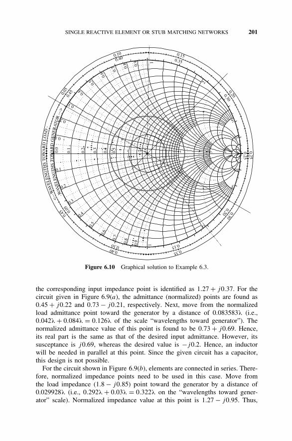
SINGLE REACTIVE ELEMENT OR STUB MATCHING NETWORKS 201
0.1
0.3
0.5
0.2
0.4
2 5 10
0.1
0.3
0.5
0.7 0.
9
0.2
0.4
0.6
0.8 1
2
5
10
0.1
0.3
0.5
0.7
0.9
0.2
0.4
0.6
0.8
1
2
5
10
0.05
0.10 0.150.20
0.25
0.30
0.350.40
0.45 0.
05
0.10 0.15
0.20
0.25
0.300.350.40
0.45
0.0
-WAV
EL
EN
GT
HS
TO
WA
RD
GE
NE
RA
TO
R--
-><-
--W
AVE
LE
NG
TH
ST
OW
AR
DL
OA
D-
Figure 6.10 Graphical solution to Example 6.3.
the corresponding input impedance point is identified as 1.27 + j0.37. For thecircuit given in Figure 6.9(a), the admittance (normalized) points are found as0.45 + j0.22 and 0.73 − j0.21, respectively. Next, move from the normalizedload admittance point toward the generator by a distance of 0.083583λ (i.e.,0.042λ + 0.084λ = 0.126λ of the scale “wavelengths toward generator”). Thenormalized admittance value of this point is found to be 0.73 + j0.69. Hence,its real part is the same as that of the desired input admittance. However, itssusceptance is j0.69, whereas the desired value is −j0.2. Hence, an inductorwill be needed in parallel at this point. Since the given circuit has a capacitor,this design is not possible.
For the circuit shown in Figure 6.9(b), elements are connected in series. There-fore, normalized impedance points need to be used in this case. Move fromthe load impedance (1.8 − j0.85) point toward the generator by a distance of0.029928λ (i.e., 0.292λ + 0.03λ = 0.322λ on the “wavelengths toward gener-ator” scale). Normalized impedance value at this point is 1.27 − j0.95. Thus,

202 IMPEDANCE-MATCHING NETWORKS
the resistance at this point is found to be equal to the value desired. However,its reactance is −j0.95, whereas the required value is j0.37. Therefore, a seriesreactance of j1.32 is needed at this point. The given circuit has an inductorthat provides a positive reactance. Hence, this circuit will work. The requiredinductance L is found as
L = 1.32 × 50
2π × 4 × 109H = 2.626 nH
6.2 DOUBLE-STUB MATCHING NETWORKS
The matching technique presented in Section 5.1 requires that a reactive elementor stub be placed at a precise distance from the load. This point will shift withload impedance. Sometimes it may not be feasible to match the load using asingle reactive element. Another possible technique to match the circuit employstwo stubs with a fixed separation between them. This device can be inserted ata convenient point before the load. The impedance is matched by adjusting thelengths of the two stubs. Of course, it does not provide a universal solution. Aswill be seen later in this section, separation between the two stubs limits therange of load impedance that can be matched with a given double-stub tuner.
Let l1 and l2 be the lengths of two stubs, as shown in Figure 6.11. The firststub is located at a distance l from the load, ZL = RL + jXL ohms. Separationbetween the two stubs is d , and the characteristic impedance of every transmissionline is Z0. In double-stub matching, the load impedance ZL is transformed tothe normalized admittance at the location of the first stub. Since the stub isconnected in parallel, its normalized susceptance is added to that and the resultingnormalized admittance is transferred to the location of the second stub. Matchingconditions at this point require that the real part of this normalized admittance
d
ZL = RL + jXL
Z0 Z0
l
l2 l1
Figure 6.11 Double-stub matching network.
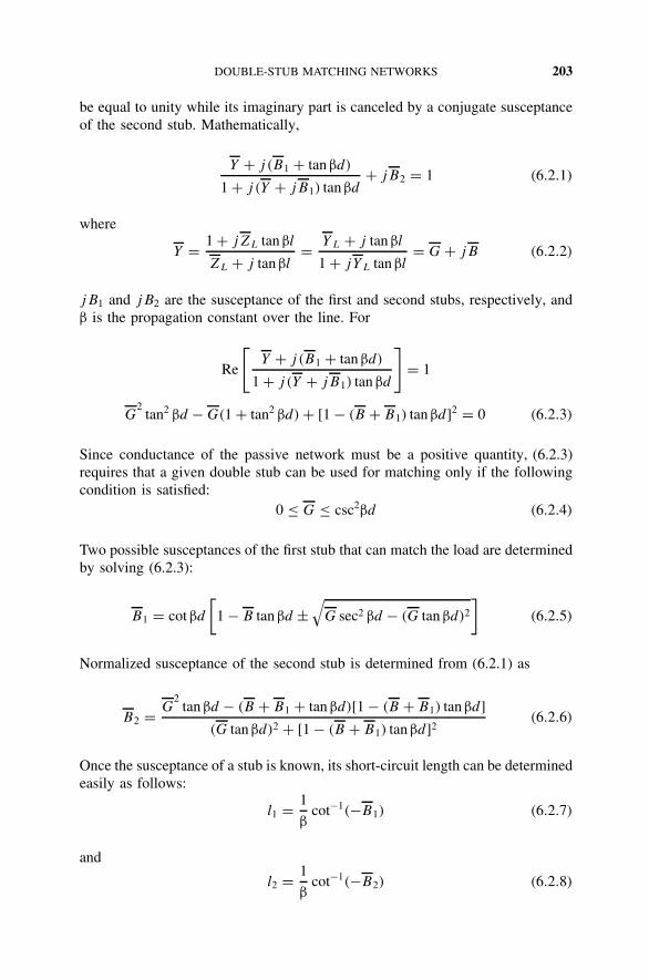
DOUBLE-STUB MATCHING NETWORKS 203
be equal to unity while its imaginary part is canceled by a conjugate susceptanceof the second stub. Mathematically,
Y + j (B1 + tan βd)
1 + j (Y + jB1) tan βd+ jB2 = 1 (6.2.1)
where
Y = 1 + jZL tan βl
ZL + j tan βl= YL + j tan βl
1 + jYL tan βl= G + jB (6.2.2)
jB1 and jB2 are the susceptance of the first and second stubs, respectively, andβ is the propagation constant over the line. For
Re
[Y + j (B1 + tan βd)
1 + j (Y + jB1) tan βd
]= 1
G2
tan2 βd − G(1 + tan2 βd) + [1 − (B + B1) tan βd]2 = 0 (6.2.3)
Since conductance of the passive network must be a positive quantity, (6.2.3)requires that a given double stub can be used for matching only if the followingcondition is satisfied:
0 ≤ G ≤ csc2βd (6.2.4)
Two possible susceptances of the first stub that can match the load are determinedby solving (6.2.3):
B1 = cot βd
[1 − B tan βd ±
√G sec2 βd − (G tan βd)2
](6.2.5)
Normalized susceptance of the second stub is determined from (6.2.1) as
B2 = G2
tan βd − (B + B1 + tan βd)[1 − (B + B1) tan βd]
(G tan βd)2 + [1 − (B + B1) tan βd]2(6.2.6)
Once the susceptance of a stub is known, its short-circuit length can be determinedeasily as follows:
l1 = 1
βcot−1(−B1) (6.2.7)
and
l2 = 1
βcot−1(−B2) (6.2.8)

204 IMPEDANCE-MATCHING NETWORKS
Graphical Method
A two-stub matching network can also be designed graphically with the help ofa Smith chart. This procedure follows the analytical concepts discussed aboveand can be summarized as follows:
1. Locate the normalized load-impedance point on a Smith chart and draw theVSWR circle. Move to the corresponding normalized admittance point. Ifthe load is connected right at the first stub, go to the next step; otherwise,move toward the generator (clockwise) by 2βl on the VSWR circle. Assumethat the normalized admittance of this point is g + jb.
2. Rotate the unity-conductance circle counterclockwise by 2βd . The conduc-tance circle that touches this circle encloses the “forbidden region.” In otherwords, this tuner can match only those Y that lie outside this circle. It is agraphical representation of the condition expressed by (6.2.4).
3. From g + jb, move on the constant-conductance circle until it intersectsthe rotated unity-conductance circle. There are at least two such points,providing two design possibilities. Let the normalized admittance of oneof these points be g + jb1.
4. The normalized susceptance required of the first stub is j (b1 − b).5. Draw a VSWR circle through point g + jb1 and move toward the generator
(clockwise) by 2βd on it. This point will fall on the unity-conductance circleof the Smith chart. Assume that this point is 1 + jb2.
6. The susceptance required from the second stub is −jb2.7. Once the stub susceptances are known, their lengths can be determined
following the procedure used in the technique described earlier.
Example 6.4 For the double-stub tuner shown in Figure 6.12, find the shortestvalues of l1 and l2 to match the load.
λ/8
ZL = 100 + j50 Ω
Z0 = 50 Ω
Z0 = 50 Ω
Z0 = 50 Ω
Z0 = 50 Ω
l2 l1
λ/8
Figure 6.12 Two-stub matching network for Example 6.4.

DOUBLE-STUB MATCHING NETWORKS 205
SOLUTION Since the two stubs are separated by λ/8, βd is equal to π/4 andthe condition (6.2.4) gives
0 ≤ G ≤ 2
This means that the real part of the normalized admittance at the first stub (load-side stub) must be less than 2; otherwise, it cannot be matched.
The graphical procedure requires the following steps to find stub settings:
1. ZL = 100 + j50
50= 2 + j1
2. Locate the normalized load impedance on a Smith chart (point A inFigure 6.13) and draw the VSWR circle. Move to the diametrically oppositeside and locate the corresponding normalized admittance point B at0.4 − j0.2.
0.1
0.3
0.5
0.2
0.4
2 5 10
0.1
0.3
0.5
0.7 0.
9
0.2
0.4
0.6
0.8 1
2
5
10
0.1
0.3
0.5
0.7
0.9
0.2
0.4
0.6
0.8
1
2
5
10
0.05
0.10 0.15
0.20
0.25
0.300.350.40
0.45 0.
050.10 0.15
0.20
0.25
0.30
0.350.40
0.45
0.0
A
B
C
D
E
F
G
-WAV
EL
EN
GT
HS
TO
WA
RD
GE
NE
RA
TO
R--
->
<---
WAV
EL
EN
GT
HS
TO
WA
RD
LO
AD
-
Figure 6.13 Smith chart solution to Example 6.4.

206 IMPEDANCE-MATCHING NETWORKS
3. Rotate the unity-conductance circle counterclockwise by 2βd = π/2 = 90.This shows that this tuner can only match the admittance with a real partof less than 2 (because it touches the constant-conductance circle of 2).
4. Move clockwise from the point 0.4 − j0.2 (0.463λ on the “wavelengthstoward generator” scale) by a distance of 2βl = π/2 = 90 or λ/8 on theVSWR circle and locate point C at 0.088λ (0.463λ + 0.125λ = 0.588λ)as the normalized admittance 0.5 − j0.5 of the load transferred to the firststub’s location.
5. From point C, move on the constant-conductance circle until it intersectsthe rotated unity-conductance circle. There are two such points, D and F.If point D is used for the design, the susceptance of the first stub must beequal to −j0.37 (i.e., j0.13 − j0.5). On the other hand, it will be j1.36(i.e., j1.86 − j0.5) for point F.
6. Locate point −j0.37 and move toward the load along the circumferenceof the Smith chart until you reach the short circuit (infinite susceptance).It gives l1 = 0.194λ. Similarly, l1 is found to be 0.4λ for j1.36.
7. Draw the VSWR circle through point D and move on it by 0.125λ (i.e.,point 0.154λ on the “wavelengths toward generator” scale). The real partof the admittance at this point (point E) is unity, and its susceptance isj0.72. Therefore, the second stub must be set for −j0.72 if the first one isset for −j0.37. Hence, the second stub is required to be 0.15λ long (i.e.,l2 = 0.15λ).
8. Draw the VSWR circle through point F and move on it by 0.125λ (0.3λ onthe “wavelengths toward generator” scale). The real part of the admittanceat this point (point G) is unity and its susceptance is −j2.7. Therefore,the second stub must be set for j2.7 if the first one is set for j1.36.In this case, the length of the second stub is found as 0.442λ (i.e., l2 =0.442λ).
9. Hence, the length of the first stub should be equal to 0.194λ and that ofthe second stub should be 0.15λ. The other possible design, where therespective lengths are found to be 0.4λ and 0.442λ, is not recommended.
Alternatively, the required stub susceptances, and hence lengths l1 and l2, canbe calculated from (6.2.2) to (6.2.8) as follows:
Y = G + jB = 0.5 + j0.5
B1 = j1.366 or − j0.366
For B1 = j1.366, B2 = j2.7321, and for B1 = −j0.366, B2 = −j0.7321. Thecorresponding lengths are found to be 0.3994λ, 0.4442λ, 0.1942λ, and 0.1494λ.These values are fairly close to those obtained graphically from the Smith chart.

MATCHING NETWORKS USING LUMPED ELEMENTS 207
6.3 MATCHING NETWORKS USING LUMPED ELEMENTS
The matching networks described so far may not be useful for certain applica-tions. For example, the wavelength of a 100-MHz signal is 3 m, and thereforeit may not be practical to use stub matching in this case because of its size ona printed circuit board. In this section we present matching networks utilizingdiscrete components that can be useful, especially in such cases. Two differ-ent types of L-section matching circuits are described here. The section beginswith resistive matching circuits that can be used for broadband applications.However, these networks dissipate signal energy and introduce thermal noise.The section ends with a presentation of the reactive matching networks that arealmost lossless, but the design is frequency dependent.
Resistive L-Section Matching Circuits
Consider a signal generator with internal resistance Rs that feeds a load resistanceRL as illustrated in Figure 6.14. Since source resistance is different from the load,a part of the signal is reflected back. Assume that Rs is larger than RL and thereis a resistive L-section introduced between the two. Further, voltages at its inputand output ports are assumed to be Vin and Vo, respectively. If this circuit ismatched at both its ports, the following two conditions must be true:
1. With RL connected, resistance looking into the input port must be Rs .
2. With Rs terminating the input port, resistance looking into the output portmust be RL.
From the first condition,
Rs = R1 + R2RL
R2 + RL
= R1R2 + R1RL + R2RL
R2 + RL
(6.3.1)
Generator Matching network Load
VsVin Vo
+ +
− −
Rs R1
R2RL
Figure 6.14 Resistive L-section matching circuit.

208 IMPEDANCE-MATCHING NETWORKS
and from the second,
RL = R2(R1 + Rs)
R2 + R1 + Rs
= R1R2 + R2Rs
R2 + R1 + Rs
(6.3.2)
Equations (6.3.1) and (6.3.2) can be solved for R1 and R2 as follows:
R1 = √Rs(Rs − RL) (6.3.3)
and
R2 =√
R2LRs
Rs − RL
(6.3.4)
The voltage across the load and the attenuation in the matching network are
Vo = Vin
R1 + R2||RL
R2||RL ⇒ Vo
Vin= R2RL
R1R2 + R1RL + R2RL
(6.3.5)
and
attenuation (dB) = 20 logR2RL
R1(R2 + RL) + R2RL
(6.3.6)
Note that R1 and R2 are real only when Rs is greater than RL. If this conditionis not satisfied (i.e., Rs < RL), the circuit shown in Figure 6.14 will requiremodification. Flipping the L-section the other way around (i.e., R1 connected inseries with RL and R2 across the input) will match the circuit. Design equationsfor that case can easily be obtained.
Example 6.5 Internal resistance of a signal generator is 75 . If it is being usedto excite a 50- transmission line, design a resistive network to match the two.Calculate the attenuation in decibels that occurs in the inserted circuit.
SOLUTION Since RL = 50 and Rs = 75 , Rs is greater than RL, and there-fore the circuit shown in Figure 6.14 can be used.
R1 = √75(75 − 50) = 43.3
R2 =√
75 × 502
75 − 50= 86.6
andattenuation (dB) = 20 log
86.6 × 50
43.3(86.6 + 50) + 86.6 × 50
= 20 log(0.4227) = −7.48 dB
The final circuit arrangement is shown in Figure 6.15.
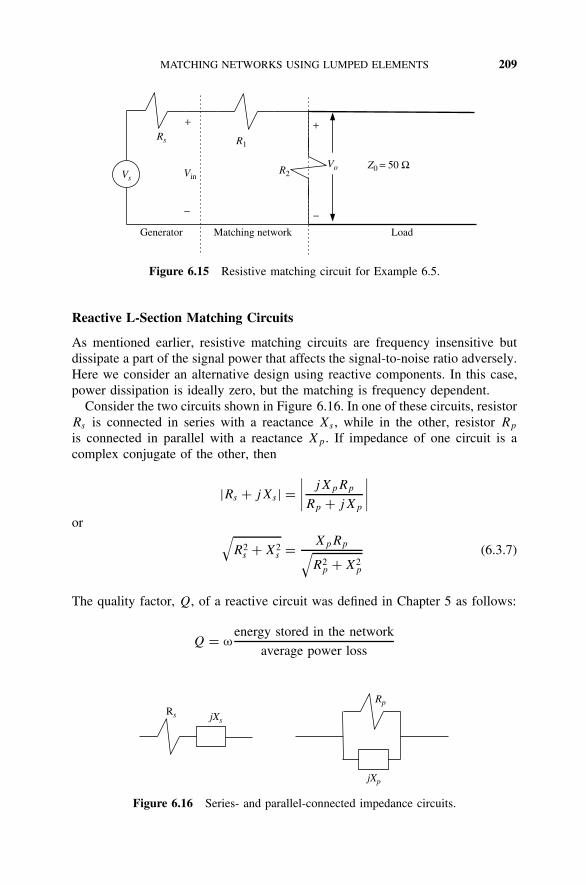
MATCHING NETWORKS USING LUMPED ELEMENTS 209
Generator Matching network Load
Vs Vin
Vo
+ +
− −
Rs R1
Z0 = 50 ΩR2
Figure 6.15 Resistive matching circuit for Example 6.5.
Reactive L-Section Matching Circuits
As mentioned earlier, resistive matching circuits are frequency insensitive butdissipate a part of the signal power that affects the signal-to-noise ratio adversely.Here we consider an alternative design using reactive components. In this case,power dissipation is ideally zero, but the matching is frequency dependent.
Consider the two circuits shown in Figure 6.16. In one of these circuits, resistorRs is connected in series with a reactance Xs , while in the other, resistor Rp
is connected in parallel with a reactance Xp. If impedance of one circuit is acomplex conjugate of the other, then
|Rs + jXs | =∣∣∣∣ jXpRp
Rp + jXp
∣∣∣∣or √
R2s + X2
s = XpRp√R2
p + X2p
(6.3.7)
The quality factor, Q, of a reactive circuit was defined in Chapter 5 as follows:
Q = ωenergy stored in the network
average power loss
Rs
Rp
jXs
jXp
Figure 6.16 Series- and parallel-connected impedance circuits.

210 IMPEDANCE-MATCHING NETWORKS
where ω is the angular frequency of the signal. For a series circuit,
Q = Xs
Rs
(6.3.8)
and for a parallel circuit,
Q = Rp
Xp
(6.3.9)
Assuming that the quality factors of these two circuits are equal, (6.3.7) can besimplified as follows:
√R2
s + R2s Q
2 = (Rp/Q)Rp√R2
p + (Rp/Q)2⇒ Rs
√1 + Q2 = Rp√
1 + Q2
Hence,
1 + Q2 = Rp
Rs
(6.3.10)
The design procedure is based on equations (6.3.8) to (6.3.10). For a resistiveload to be matched with another resistor (it may be a transmission line or gener-ator), Rp and Rs are defined such that the former is greater. Q of the circuit isthen calculated from (6.3.10). Respective reactances are subsequently determinedfrom (6.3.8) and (6.3.9). If one reactance is selected capacitive, the other mustbe inductive. Xp will be connected in parallel with Rp, and Xs will be in serieswith Rs . The following example illustrates the procedure.
Example 6.6 Design a reactive L-section that matches a 600- resistive loadto a 50- transmission line. Determine the component values if the matching isdesired at 400 MHz.
SOLUTION Since Rp must be larger than Rs , the 600- load is selected asRp and a 50- line as Rs . Hence, from (6.3.10) we have
Q2 + 1 = Rp
Rs
= 600
50= 12 ⇒ Q = √
11 = 3.3166
Now, from (6.3.8) and (6.3.9),
Xs = QRs = 3.3166 × 50 = 165.8312
Xp = Rp
Q= 600
3.3166= 180.9068

MATCHING NETWORKS USING LUMPED ELEMENTS 211
or50 Ω
600 ΩXp
Xs
(1)
50 Ω
600 Ω
Xp
Xs
(2)
Figure 6.17 Design of two reactive matching circuits for Example 6.6.
Therefore, either one of the two circuits in Figure 6.17 can be used to match theload with the line.
For circuit (1) in Figure 6.17, the component values are determined as follows:
Xs = 165.8312 = 1
ωCs
Therefore,
Cs = 1
2π × 400 × 106 × 165.8312≈ 2.4 × 10⁻¹² F = 2.4 pF
andXp = 180.9068 = ωLp
Therefore,
Lp = 180.9068
2π × 400 × 106= 71.9805 × 10⁻⁹ H ≈ 72 nH
Similarly, the component values for circuit (2) in Figure 6.17 are
Xs = 165.8312 = ωLs
Therefore,
Ls = 165.8312
2π × 400 × 106= 65.9821 × 10⁻⁹ H ≈ 66 nH
and
Xp = 180.9068 = 1
ωCp
Therefore,
Cp = 1
2π × 400 × 106 × 180.9068= 2.2 × 10⁻¹² F = 2.2 pF

212 IMPEDANCE-MATCHING NETWORKS
Example 6.7 Consider Example 6.6 again and transform a 600- resistive loadto a 173.2- load by adjusting the Q value of a matching circuit. Continuethe transformation process to get 50 from 173.2 . Compare the frequencyresponse (reflection coefficient versus frequency) of your circuits.
SOLUTION For the first part of this example, Rp is 600 and Rs is 173.2 .Hence, from (6.3.8) to (6.3.10),
Q =√
Rp
Rs
− 1 =√
600
173.2− 1 = 1.569778
Xs = QRs = 271.8856
and
Xp = Rp
Q= 382.2196
Repeating the calculations with Rp = 173.2 and Rs = 50 , for the secondpart of the example we get
Q =√
Rp
Rs
− 1 =√
173.2
50− 1 = 1.5697
This value of Q is very close to that obtained earlier. This is because 173.2 isclose to the geometric mean of 600 and 50. Hence,
Xs = QRs = 78.4857
and
Xp = Rp
Q= 110.3386
Two of the possible circuits (3) and (4) are shown in Figure 6.18 along with theircomponent values. For these circuits, the impedance that the 50- transmissionline sees can be determined. The reflection coefficient is then determined for eachcase. This procedure is repeated for the circuits obtained in Example 6.6 as well.Magnitude of the reflection coefficient for each of these four cases is displayed inFigure 6.19. Curves (a) and (b) are obtained for circuits (1) and (2) of Figure 6.17,respectively. The frequency response of circuit (3) in Figure 6.18 is illustratedby curve (c) of Figure 6.19, while curve (d) displays the frequency response ofcircuit (4). The horizontal axis of Figure 6.19 represents the normalized frequency(i.e., the signal frequency divided by 400 MHz).
As Figure 6.19 indicates, the reflection coefficient is zero for all four circuitsat a normalized frequency of unity. However, it increases if the signal frequencyis changed on either side. Further, the rate of increase in reflection is higherfor circuits obtained in Example 6.6. For example, if a reflection coefficient of

MATCHING NETWORKS USING LUMPED ELEMENTS 213
600 Ω 600 Ω 50 Ω50 Ω 2.2 pF3.61 pF
2.4 pF 5.07 pF
72 nH43.9 nH
66 nH31.23 nH
(3) (4)
Figure 6.18 Design of reactive matching networks for Example 6.7.
0.0 0.5 1.0 1.5 2.0
Normalized frequency
0.0
0.2
0.4
0.6
0.8
1.0(a)
(b)
(c)
(d)ρ
Figure 6.19 Reflection coefficient (magnitude) versus normalized frequency for thematching circuits designed in Examples 6.6 and 6.7.
0.2 is acceptable, circuits (3) and (4) can provide a much wider bandwidth thanthose of Example 6.6. This concept can be used to shape the reflection coefficientcharacteristics over the desired frequency band.
Example 6.8 A 50- transmission line is to be matched with a 10 +j10-load. Design two different L-section reactive circuits and find the componentvalues at 500 MHz.
SOLUTION Unlike the cases considered so far, the load is complex in thisexample. However, the same design procedure is still applicable. We consideronly the real part of load impedance initially and take its imaginary part intoaccount later in the design. Since characteristic impedance of the transmissionline is greater than the real part of the load (i.e., 50 > 10 ), Rp is 50 whileRs is 10 . Therefore,
Q2 = 50
10− 1 = 4 ⇒ Q = 2

214 IMPEDANCE-MATCHING NETWORKS
Xs and Xp can now be determined from (6.3.8) and (6.3.9):
Xs = QRs = 2 × 10 = 20
and
Xp = Rp
Q= 50
2= 25
Reactance Xp is connected in parallel with the transmission line and Xs is inseries with the load. These two matching circuits are shown in Figure 6.20. If Xp
is a capacitive reactance of 25 , Xs must be inductive 20 . The reactive partthat has not been taken into account so far needs to be included at this point inXs . Since this reactive part of the load is inductive 10 , another series inductorfor the remaining 10 is needed, as shown in circuit (1) of Figure 6.20. Hence,
ωLs = 20 − 10
Therefore,
Ls = 10
2π × 500 × 106H = 0.3183 × 10⁻⁸ H = 3.183 nH
and1
ωCp
= 25
Therefore,
Cp = 1
2π × 500 × 106 × 25= 0.0127324 × 10⁻⁹ F = 12.7324 pF
In the second case, Xp is assumed inductive and therefore Xs needs to be capac-itive. It is circuit (2) in Figure 6.20. Since the load has a 10- inductive reactance,
Load
10 Ω
j10 Ω50 Ω
Cp
Ls
Load
10 Ω
j10 Ω50 Ω
Cs
Lp
(1) (2)
Figure 6.20 Reactive matching circuits for Example 6.8.

MATCHING NETWORKS USING LUMPED ELEMENTS 215
it must be taken into account in determining the required capacitance. Therefore,
ωCs = 1
20 + 10⇒ Cs = 1
2π × 500 × 106 × 30F = 10.61 pF
and
ωLp = 25 ⇒ Lp = 25
2π × 500 × 106H = 7.9577 nH
The matching procedure used so far is based on the transformation of seriesimpedance to a parallel circuit of the same quality factor. Similarly, one can usean admittance transformation, as shown in Figure 6.21.
These design equations can be obtained easily following the procedure usedearlier:
Gs
Gp
= 1 + Q2 (6.3.11)
Q = Gs
Bs
(6.3.12)
and
Q = Bp
Gp
(6.3.13)
Note from (6.3.11) that Gs must be greater than Gp for a real Q.
Example 6.9 A load admittance, YL = 8 − j12 mS, is to be matched with a50- line. There are three different L-section matching networks given to you,as shown in Figure 6.22. Complete or verify each of these circuits. Find theelement values at 1 GHz.
SOLUTION Since the characteristic impedance of the line is 50 , the cor-responding conductance will be 0.02 S. The real part of the load admittanceis 0.008 S. Therefore, Gs must be 0.02 S in (6.3.11). However, the circuits inFigure 6.22 have a capacitor or an inductor connected in parallel with the 50-line. Obviously, these design equations cannot be used here. Equations (6.3.8)
GsGp
jBs
jBp
Figure 6.21 Series- and parallel-connected admittance circuits.
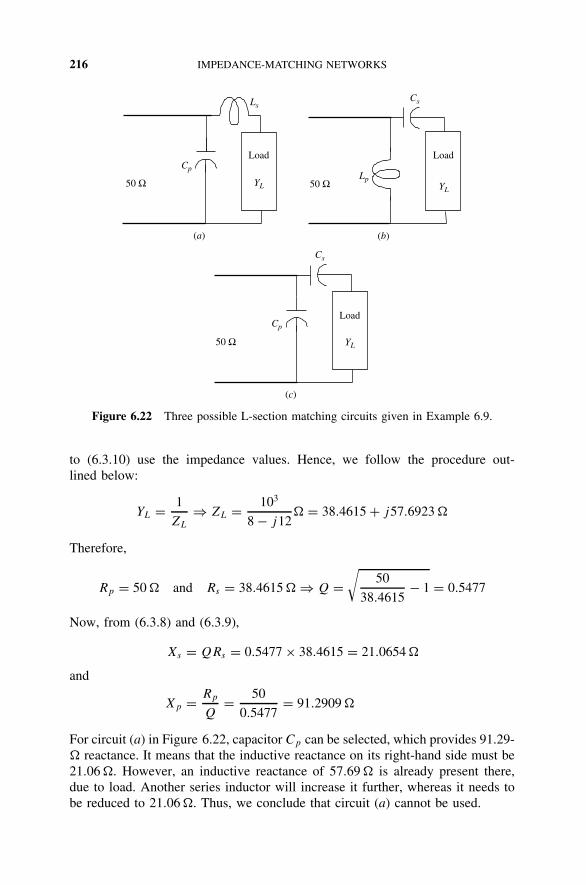
216 IMPEDANCE-MATCHING NETWORKS
50 Ω
Cp
Ls
Load
YL
(a)
50 Ω
Cs
Lp
Load
YL
(b)
50 Ω
Cp
Cs
Load
YL
(c)
Figure 6.22 Three possible L-section matching circuits given in Example 6.9.
to (6.3.10) use the impedance values. Hence, we follow the procedure out-lined below:
YL = 1
ZL
⇒ ZL = 103
8 − j12 = 38.4615 + j57.6923
Therefore,
Rp = 50 and Rs = 38.4615 ⇒ Q =√
50
38.4615− 1 = 0.5477
Now, from (6.3.8) and (6.3.9),
Xs = QRs = 0.5477 × 38.4615 = 21.0654
and
Xp = Rp
Q= 50
0.5477= 91.2909
For circuit (a) in Figure 6.22, capacitor Cp can be selected, which provides 91.29- reactance. It means that the inductive reactance on its right-hand side must be21.06 . However, an inductive reactance of 57.69 is already present there,due to load. Another series inductor will increase it further, whereas it needs tobe reduced to 21.06 . Thus, we conclude that circuit (a) cannot be used.

MATCHING NETWORKS USING LUMPED ELEMENTS 217
In circuit (b) in Figure 6.22, there is an inductor in parallel with the transmis-sion line. For a match, its reactance must be 91.29 , and overall reactance tothe right must be capacitive 21.06 . Inductive reactance of 57.69 of the loadneeds to be neutralized as well. Hence,
Xc = 57.6923 + 21.0654 = 78.7577
Therefore,
C = 1
2π × 109 × 78.7577F = 2.0208 pF
and
Xp = 91.2909 ⇒ L = 91.2909
2π × 109H = 14.5294 nH
Circuit (c) in Figure 6.22 has a capacitor across the transmission line terminals.Assuming that its reactance is 91.29 , reactance to the right must be inductive21.06 . As noted before, the reactive part of the load is an inductive 57.69 . Itcan be reduced to the desired value by connecting a capacitor in series. Hence,the component values for circuit (c) are calculated as follows:
Xs = 57.6923 − 21.0654 = 36.6269
Therefore, Cs = 4.3453 pF and
Xp = 91.2909 ⇒ Cp = 1.7434 pF
Example 6.10 Reconsider Example 6.9, where YL = 8 −j12 mS is to bematched with a 50- line. Complete or verify the L-section matching circuitsshown in Figure 6.23 at a signal frequency of 1 GHz.
50 Ω
Cp
Ls
Load
YL
(a) (b)
50 Ω
Cs
Cp
Load
YL
Figure 6.23 L-section matching networks given in Example 6.10.

218 IMPEDANCE-MATCHING NETWORKS
SOLUTION As noted in Example 6.9, Gs is 0.02 S and Gp is 8 mS. Lookingover the given circuit configurations, it seems possible to complete or verify thesecircuits through (6.3.11) to (6.1.13). Hence,
Q =√
Gs
Gp
− 1 =√
0.02
0.008− 1 = 1.2247
Bs = Gs
Q= 0.02
1.2247= 0.0163 S
and
Bp = QGp = 1.2247 × 0.008 = 0.0097978 ≈ 0.01 S
If Bs is selected as an inductive susceptance, Bp must be capacitive. Since loadhas an inductive susceptance of 12 mS, the capacitor must neutralize that, too.Hence, circuit (a) of Figure 6.23 will work provided that
Bs = 0.0163 S ⇒ Ls = 9.746 nH
and
Bp = (0.01 + 0.012) S = 0.022 S ⇒ Cp = 3.501 pF
In circuit (b) of Figure 6.23, a capacitor is connected in series with Gs . Therefore,Bp must be an inductive susceptance. Since it is 0.012 S whereas only 0.01 S isrequired for matching, a capacitor in parallel is needed. Hence,
Bs = 0.0163 S ⇒ Cs = 2.599 pF
and
Bp = (0.012 − 0.01) = 0.002 S (capacitive) ⇒ Cp = 0.3183 pF
Thus, both circuits can work provided that the component values are as foundabove.
Graphical Method
As described earlier, L-section reactive networks can be used for matching theimpedance. One of these reactive elements appears in series with the load or thedesired impedance, while the other one is connected in parallel. Thus, the resis-tive part stays constant when a reactance is connected in series with impedance.Similarly, a change in the shunt-connected susceptance does not affect the con-ductive part of the admittance. Consider the normalized impedance point X onthe Smith chart shown in Figure 6.24. To distinguish it from others, it may becalled the Z-Smith chart. If its resistive part needs to be kept constant at 0.5,one must stay on this constant-resistance circle. A clockwise movement from

MATCHING NETWORKS USING LUMPED ELEMENTS 219
0
0.2
0.5 1 2 5 10
180
170
160
150
140
130120
110100 90 80 70
6050
40
3020
100
−10−20
−30−40
−50−60
−70−80−90−100−110−120−130
−140
−150
−160
−170Capacitive
reactance
Inductivereactance
jX
-jX
Capacitive reactance
Inductive reactance
X
Figure 6.24 Impedance (Z-) Smith chart.
this point increases the positive reactance. It means that the inductance increasesin series with the impedance of X. On the other hand, the positive reactancedecreases with a counterclockwise movement. A reduction in positive reactancemeans a decrease in series inductance or an increase in series capacitance. Notethat this movement also represents an increase in negative reactance.
Now consider a Smith chart that is rotated by 180 from its usual position,as shown in Figure 6.25. It may be called a Y -Smith chart because it representsthe admittance plots. In this case, addition (or subtraction) of a susceptance toadmittance does not affect its real part. Hence, it represents a movement on theconstant-conductance circle. Assume that a normalized admittance is located atpoint X. The conductive part of this admittance is 0.5. If a shunt inductance isadded, it moves counterclockwise on this circle. On the other hand, a capacitivesusceptance moves this point clockwise on the constant-conductance circle.
A superposition of Z- and Y -Smith charts is shown in Figure 6.26. It is generallyreferred to as a ZY -Smith chart because it includes impedance as well as admittanceplots at the same time. A short-circuit impedance is zero while the correspondingadmittance goes to infinity. A single point on the ZY -Smith chart represents it.Similarly, it may be found that other impedance points of the Z chart coincidewith the corresponding admittance points of the Y chart as well. Hence, impedance

220 IMPEDANCE-MATCHING NETWORKS
0
0.2
0.512510 18
017
016
0
150
140
130
120
1101009080
70
60
50
40
30
2010
0−10
−20
−30
−40
−50
−60
−70−80 −90 −100
-110
−120
−130
−140
−150
−160
−170
jB
-jB
Capacitivesusceptance
Inductivesusceptance
Inductive susceptance
Capacitive susceptance
X
Figure 6.25 Admittance (Y -) Smith chart..
can be transformed to corresponding admittance just by switching from the Z- tothe Y -scales of a ZY -Smith chart. For example, a normalized impedance point of0.9 − j1 is located using the Z-chart scales as A in Figure 6.26. The correspondingadmittance is read from a Y -chart as 0.5 + j0.55.
Reactive L-section matching circuits can be designed easily using a ZY -Smithchart. Load and desired impedance points are identified on this chart using Z-scales. Y -scales may be used if either one is given as admittance. Note that thesame characteristic impedance is used for normalizing these values. Now, movefrom the point to be transformed toward the desired point following a constant-resistance or constant-conductance circle. Movement on the constant-conductancecircle gives the required susceptance (i.e., a reactive element will be needed inshunt). It is determined by subtracting initial susceptance (the starting point)from the value reached. When moving on the conductance circle, use the Y -scaleof the chart. Similarly, moving on a constant-resistance circle will mean that areactance must be connected in series. It can be determined using the Z-scale ofthe ZY -Smith chart.

MATCHING NETWORKS USING LUMPED ELEMENTS 221
0
0.2
0.5 1 2 5 10
180
170
160
150
140
130120
110100 90 80
7060
50
40
3020
100
−10−20
−30−40
−50−60
−70−80−90−100−110
−120−130
−140
−150
−160
−170
A
Figure 6.26 ZY -chart.
Note from the ZY -chart that if a normalized load value falls inside the unityresistance circle, it can be matched with the characteristic impedance Z0 onlyafter shunting it with an inductor or capacitor (a series-connected inductor orcapacitor at the load will not work). Similarly, a series inductor or capacitoris required at the load if the normalized value is inside the unity conductancecircle. Outside these two unity circles, if the load point falls in the upper half,the first component required for matching would be a capacitor that can be seriesor parallel connected. On the other hand, an inductor will be needed at the loadfirst if the load point is located in the lower half and outside the unity circles.
Example 6.11 Use a ZY -Smith chart to design the matching circuits ofExamples 6.9 and 6.10.

222 IMPEDANCE-MATCHING NETWORKS
SOLUTION In this case the given load admittance can be normalized by thecharacteristic admittance of the transmission line. Hence,
YL = YL
Y0= YLZ0 = 0.4 − j0.6
This point is found on the ZY -Smith chart as A in Figure 6.27. The matchingrequires that this admittance must be transformed to 1. This point can be reachedthrough a unity conductance or resistance circle. Hence, a matching circuit canbe designed if somehow we can reach one of these circles through constant-resistance and constant-conductance circles only. Since constant-conductancecircles intersect constant- resistance circles, one needs to start on a constant-
0
0.2
0.5 1 2 5 1018
017
016
015
014
0
130
120110
100 90 8070
60
50
40
3020
100
−10−20
−30−40
−50
−60−70
−80−90−100−110−120
−130
−140
−150
−160
−170
A
B
D
C
E
O
Figure 6.27 Graphical solution to Example 6.11.

MATCHING NETWORKS USING LUMPED ELEMENTS 223
resistance circle to get on the unity conductance circle, or vice versa. There aretwo circles (i.e., 0.4 conductance and 0.78 resistance circles) passing throughpoint A. Hence, it is possible to get on to the unity resistance circle via the0.4 conductance circle. Alternatively, one can reach on the unity conductancecircle through the 0.78 resistance circle. In either case, a circuit can be designed.From point A, one can move on the 0.4 conductance circle (or 0.78 resistancecircle) so that the real part of the admittance (or impedance) remains constant.If we start counterclockwise from A on the conductance circle, we end up atinfinite susceptance without intersecting the unity resistance circle. Obviously,this does not yield a matching circuit. Similarly, a clockwise movement on the0.78 resistance circle from A cannot produce a matching network. Hence, aninductor in parallel or in series with the given load cannot be used for the designof a matching circuit. This proves that the circuit shown in Figure 6.22(a) cannotbe designed.
There are four possible circuits. In one case, move from point A to B onthe conductance circle (a shunt capacitor) and then from B to O on the unityresistance circle (a series capacitor). The second possibility is via A to C (ashunt capacitor) and then from C to O (a series inductor). A third circuit can beobtained following the path from A to D (a series capacitor) and then from Dto O (a shunt capacitor). The last circuit can be designed by following the pathfrom A to E (a series capacitor) and then from E to O (a shunt inductor). A–Eto E–O and A–D to D–O correspond to the circuits shown in Figure 6.22(b)and (c), respectively. Similarly, A–C to C–O and A–B to B–O correspondto circuits shown in Figure 6.23(a) and (b), respectively. Component values foreach of these circuits are determined following the corresponding susceptanceor reactance scales. For example, we move along a resistance circle from A toD. That means that there will be a change in reactance. The required elementvalue is determined after subtracting the reactance at A from the reactance at D.This difference is j0.42 − j1.15 = −j0.73. Negative reactance means that it isa series capacitor. Note that −j0.73 is a normalized value. The actual reactanceis −j0.73 × 50 = −j36.5 . It is close to the corresponding value of 36.6269
obtained earlier. Other components can be determined as well.
Example 6.12 Two types of L-section matching networks are shown inFigure 6.28. Select one that can match the load ZL = 25 + j10 to a 50-transmission line. Find the element values at 500 MHz.
SOLUTION First, let us consider circuit (a). Rp must be 50 because it isrequired to be greater than Rs . However, the reactive element is connectedin series with it. That will be possible only with Rs . Hence, this circuitcannot be designed using (6.3.8) to (6.3.10). The other set of design equations,namely, (6.3.11) to (6.3.13), requires admittance instead of impedance. Therefore,the given impedances are inverted to find the corresponding admittances as

224 IMPEDANCE-MATCHING NETWORKS
(a) (b)
Z0 = 50 Ω Z0 = 50 Ω
CsLs
Lp CpZL ZL
Figure 6.28 L-section matching circuits given for Example 6.12.
follows:
YL = 1
ZL
= 1
25 + j10= 0.034483 − j0.01379 S
and
Y0 = 1
Z0= 1
50= 0.02 S
Since Gs must be larger than Gp, this set of equations produces a matchingcircuit that has a reactance in series with YL. Thus, we conclude that the circuitgiven in Figure 6.28(a) cannot be designed.
Now consider the circuit shown in Figure 6.28(b). For (6.3.8) to (6.3.10), Rp
is 50 while Rs is 25 . Hence, one reactance of the matching circuit will beconnected across 50 and the other one will go in series with ZL. The givencircuit has this configuration. Hence, it will work. Its component values arecalculated as
Q =√
50
25− 1 = 1
Therefore,
Xs = Rs = 25
and
Xp = Rp = 50
For Xp to be capacitive, we have
1
ωCp
= 50 ⇒ Cp = 6.366 pF

MATCHING NETWORKS USING LUMPED ELEMENTS 225
As 10 of inductive reactance is already included in the load, another inductive15 will suffice. Thus,
ωLs = 25 − 10 = 15 ⇒ Ls = 15
ωH = 4.775 nH
This example can be solved using a ZY -Smith chart as well. To that end, theload impedance is normalized with characteristic impedance of the line. Hence,
ZL = 25 + j10
50= 0.5 + j0.2
This point is located on a ZY -Smith chart as shown in Figure 6.29. It is pointA on this chart. If we move on the conductance circle from A, we never reach
0
0.2
0.5 1 2 5
10
180
170
160
150
140
130120
110100 90 80
7060
50
40
3020
100
−10−20
−30−40
−50−60
−70−80−90−100−110
−120−130
−140
−150
−160
−170
B
A
O
Figure 6.29 Graphical solution to Example 6.12.

226 IMPEDANCE-MATCHING NETWORKS
the unity-resistance circle. This means that an L-section matching circuit that hasa reactance (inductor or capacitor) in parallel with the load cannot be designed.Therefore, circuit (a) of Figure 6.28 is not possible.
Next, we try a reactance in series with the load. Moving on the constant-resistance circle from A indicates that there are two possible circuits. Movementfrom A to B on the resistance circle and then from B to O on the unity con-ductance circle provides component values of circuit shown in Figure 6.28(b).The normalized reactance required is found to be j0.3 (i.e., j0.5 − j0.2). Itis an inductor because of its positive value. Further, it will be connected inseries with the load because it is found by moving on a constant-resistance circlefrom A.
The series inductance required is determined as
XL = 0.3 × 50 = 15 ⇒ Ls = 15
ωH = 4.775 nH
Movement from B to O gives a normalized susceptance of j1. Positive suscep-tance is a capacitor in parallel with a 50- line. Hence,
ωCp = 1
50⇒ Cp = 6.366 pF
These results are found to be exactly equal to those found earlier analytically.
SUGGESTED READING
Bahl, I., and P. Bhartia, Microwave Solid State Circuit Design. New York: Wiley, 1988.
Collin, R. E., Foundations for Microwave Engineering. New York: McGraw-Hill, 1992.
Fusco, V. F., Microwave Circuits. Englewood Cliffs, NJ: Prentice Hall, 1987.
Pozar, D. M., Microwave Engineering. New York: Wiley, 1998.
Ramo, S., J. R. Whinnery, and T. Van Duzer, Fields and Waves in Communication Elec-tronics. New York: Wiley, 1994.
Rizzi, P. A., Microwave Engineering, Englewood Cliffs, NJ: Prentice Hall, 1988.
Sinnema, W., Electronic Transmission Technology. Englewood Cliffs, NJ: Prentice Hall,1988.
PROBLEMS
6.1. A 10-V (rms) voltage source in series with a 50- resistance represents asignal generator. It is to be matched with a 100- load. Design a matchingcircuit that provides perfect matching over the frequency band 1 kHz to1 GHz. Determine the power delivered to the load.

PROBLEMS 227
6.2. A 1000- load is to be matched with a signal generator that can be repre-sented by a 1-A (rms) current source in parallel with a 100- resistance.Design a resistive circuit to match it. Determine the power dissipated inthe matching network.
6.3. Design a single-stub network to match a 800 −j300- load to a 400-lossless line. The stub should be located as close to the load as possibleand it is to be connected in parallel with the transmission line.
6.4. A 140 −j70- load is terminating a 70- transmission line, as shownin Figure P6.4. Find the location and length of a short-circuited stub of a40- characteristic impedance that will match the load with the line.
40 Ω
140 − j70 Ω
70 Ω 70 Ω
S.C.
Figure P6.4
6.5. An antenna has impedance of 40 +j30 at its input. Match it with a 50- line using short-circuited shunt stubs. Determine (a) the required stubadmittance, (b) the distance between the stub and the antenna, (c) the stublength, and (d) the VSWR on each section of the circuit.
6.6. A lossless 100- transmission line is to be matched with a 100 +j100- load using a double-stub tuner (Figure P6.6). Separation between thetwo stubs is λ/8 and the characteristic impedance is 100 . A load isconnected right at the location of the first stub. Determine the shortestpossible lengths of the two stubs to obtain the matched condition, and findthe VSWR between the two stubs.

228 IMPEDANCE-MATCHING NETWORKS
100 Ω
100 + j100 Ω
λ/8
Figure P6.6
6.7. A lossless 75- transmission line is to be matched with a 150 +j15-load using a shunt-connected double-stub tuner. Separation between thetwo stubs is λ/8 and the characteristic impedance is 75 . The stub closestto the load (first stub) is λ/2 away from it. Determine the shortest possiblelengths of the two stubs to obtain the matched condition, and find theVSWR between the two stubs.
6.8. A lossless 50- transmission line is to be matched with a 25 +j50- loadusing a double-stub tuner. Separation between the two stubs is 3λ/8 and thecharacteristic impedance is 50 . A load is connected at 0.2λ from the firststub, as shown in Figure P6.8. Determine the shortest possible lengths ofthe two stubs to obtain the matched condition, and find the VSWR betweenthe two stubs.
3λ/8
ZL = 25 + j50 Ω
l2l1
0.2λ
Z0 = 50 Ω Z0 = 50 Ω
Z0 = 50 Ω
Z0 = 50 Ω
Figure P6.8

PROBLEMS 229
6.9. Complete or verify the two interstage designs of 1 GHz shown as (a) and(b) in Figure P6.9.
~0.174λ
(a)
Γin = 0.29 ∠40°
ΓL = 0.58 ∠20°
Matchingnetwork
(b)
O.C.
~0.086λ
Figure P6.9
6.10. Determine the shortest length d in the two networks in Figure P6.10 tomatch the load to a 50- lossless line. Also find the stub length l forcircuit (a) and the required inductance L for circuit (b).
(a) (b)
ΓL = 0.3 ∠45° ΓL = 0.3 ∠45°
ZL ZL
O.C. stub
L
dd
Figure P6.10

230 IMPEDANCE-MATCHING NETWORKS
6.11. Determine the shortest length d in the two networks in Figure P6.11 tomatch a 100 −j50- load to a 50- lossless line. Also find the requiredcapacitance C for circuit (a) and the stub length l for circuit (b).
(a) (b)
ZL
C
d d
50 Ω ZL50 Ω
l
Figure P6.11
6.12. Complete or verify the two interstage designs of 1 GHz shown as (a) and(b) in Figure P6.12. Assume that the characteristic impedance is 50 .
Γin = 1/3 ∠−120°
ΓL = 2/3 ∠50°
Matchingnetwork
(b)
~0.1λ
O.C.
(a)
d
CSeries stub
Figure P6.12
6.13. Complete or verify the interstage designs at f = 4 GHz, shown as (a) and(b) in Figure P6.13.

PROBLEMS 231
LoadMatchingnetwork
(b) (a)
ZL
C L ZL
d d
ΓL = 0.3 ∠−90°
Γin = 0.3 ∠45°
Γin = 0.3 ∠45°Γin = 0.3 ∠45°
Figure P6.13
6.14. Complete or verify the interstage designs at f = 4 GHz shown as (a) and(b) in Figure P6.14. The characteristic impedance is 50 .
~0.385λ0.126λ
ZL
C
ZL
L
ΓL = 5/9∠−150°
Γin = 3/7 ∠80°
Γin = 3/7 ∠80° Γin = 3/7 ∠ 80°
(a) (b)
Figure P6.14
6.15. Two types of L-section matching networks are shown in Figure P6.15.Select one that can match the load ZL = 20 −j100 to a 50- transmis-sion line. Find the element values at 500 MHz.

232 IMPEDANCE-MATCHING NETWORKS
(b)
C
ZLL50 Ω
(a)
ZLLp
Ls
50 Ω
Figure P6.15
6.16. Two types of L-section matching networks are shown in Figure P6.16.Select one that can match a 30 +j50- load to a 50- line at 1 GHz.
ZL ZLL
CC1
C2
50 Ω 50 Ω
(a) (b)
Figure P6.16
6.17. Design a matching network (Figure P6.17) that will transform a 50 −j50-load to the input impedance of 25 +j25 .
Zin = 25 + j25 Ω ZL = 50 − j50 ΩMatchingnetwork
Figure P6.17
6.18. Match the load in Figure P6.18 to a 50- generator using lumped elements.Assume that the signal frequency as 4 GHz.
LoadMatchingnetwork
ΓL = 0.5 ∠45°
Γin = 0
Figure P6.18

PROBLEMS 233
6.19. Two types of L-section matching networks are shown in Figure P6.19.Select one that can match the load ZL = 60 −j20 to a 50- transmissionline. Find the element values at 500 MHz.
50 Ω 50 ΩCp
Ls Ls
ZL Cp ZL
(a) (b)
Figure P6.19
6.20. Design a lumped-element network that will provide a load ZL = 30 +j50
for the amplifier shown in Figure P6.20 operating at 2 GHz.
AmplifierLumpedelements 50 Ω
ZL
Figure P6.20
6.21. Design a lumped-element network that will provide a load ZL = 30 +j50
for the amplifier shown in Figure P6.21, and stop the biasing voltage fromappearing across 50 . The amplifier is operating at 500 MHz.
AmplifierLumpedelements 50 Ω
ZL
Figure P6.21
6.22. A 200- load is to be matched with a 50- line. Design (a) a resistivenetwork and (b) a reactive network to match the load. (c) Compare theperformance of the two designs.

7IMPEDANCE TRANSFORMERS
In Chapter 6, several techniques were considered to match a given load impedanceat a fixed frequency. These techniques included transmission line stubs as wellas lumped elements. Note that lumped-element circuits may not be practicalat higher frequencies. Further, it may be necessary in certain cases to keep thereflection coefficient below a specified value over a given frequency band. In thischapter we present transmission line impedance transformers that can meet suchrequirements. The chapter begins with a single-section impedance transformerthat provides perfect matching at a single frequency. A matching bandwidth canbe increased at the cost of a higher reflection coefficient. This concept is used todesign multisection transformers. The characteristic impedance of each sectionis controlled to obtain the desired passband response.
Multisection binomial transformers exhibit an almost flat reflection coefficientabout the center frequency and increase gradually on either side. A wider band-width is achieved with an increased number of quarter-wave sections. Chebyshevtransformers can provide even wider bandwidth with the same number of sections,but the reflection coefficient exhibits ripples in its passband. The chapter includesa procedure to design these multisection transformers as well as transmission linetapers. The chapter concludes with a brief discussion on the Bode–Fano con-straints, which provide an insight into the trade-off between the bandwidth andthe allowed reflection coefficient.
7.1 SINGLE-SECTION QUARTER-WAVE TRANSFORMERS
We considered a single-section quarter-wavelength transformer design problemin Example 3.5. In this section we present a detailed analysis of such circuits.
Radio-Frequency and Microwave Communication Circuits: Analysis and Design, Second Edition,By Devendra K. MisraISBN 0-471-47873-3 Copyright 2004 John Wiley & Sons, Inc.
234
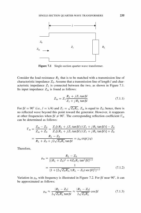
SINGLE-SECTION QUARTER-WAVE TRANSFORMERS 235
Z1
l
Z0
RLZin
Figure 7.1 Single-section quarter-wave transformer.
Consider the load resistance RL that is to be matched with a transmission line ofcharacteristic impedance Z0. Assume that a transmission line of length l and char-acteristic impedance Z1 is connected between the two, as shown in Figure 7.1.Its input impedance Zin is found as follows:
Zin = Z1RL + jZ1 tan βl
Z1 + jRL tan βl(7.1.1)
For βl = 90 (i.e., l = λ/4) and Z1 = √Z0RL, Zin is equal to Z0; hence, there is
no reflected wave beyond this point toward the generator. However, it reappearsat other frequencies when βl = 90. The corresponding reflection coefficient in
can be determined as follows:
in = Zin − Z0
Zin + Z0= Z1[(RL + jZ1 tan βl)/(Z1 + jRL tan βl)] − Z0
Z1[(RL + jZ1 tan βl)/(Z1 + jRL tan βl)] + Z0
= RL − Z0
RL + Z0 + j2√
Z0RL tan βl= ρin exp(jϕ)
Therefore,
ρin = RL − Z0
[(RL + Z0)2 + 4Z0RL tan2 βl]1/2
= 1
1 + [2√
Z0RL/(RL − Z0) sec βl]21/2(7.1.2)
Variation in ρin with frequency is illustrated in Figure 7.2. For βl near 90, it canbe approximated as follows:
ρin ≈ |RL − Z0|2√
Z0RL tan βl≈ |RL − Z0|
2√
Z0RL
cos βl (7.1.3)

236 IMPEDANCE TRANSFORMERS
0.0 0.5 1.0 1.5 2.0 2.5 3.0 3.50.00
0.05
0.10
0.15
0.20
0.25
0.30
0.35
βl
ρ in
ρMθ1 π − θ1
Figure 7.2 Reflection coefficient characteristics of a single-section impedance trans-former used to match a 100- load to a 50- line.
If ρM is the maximum allowable reflection coefficient at the input, then
cos θ1 =
∣∣∣∣∣∣∣2ρM
√Z0RL
(RL − Z0)
√1 − ρ2
M
∣∣∣∣∣∣∣ θ1 <π
2(7.1.4)
In the case of a TEM wave propagating on the transmission line, βl = (π/2)
(f/f0), where f0 is the frequency at which βl = π/2. In this case, the bandwidthf2 − f1 = f is given by
f = (f2 − f1) = 2(f0 − f1) = 2
(f0 − 2f0
πθ1
)(7.1.5)
and the fractional bandwidth is
f
f0= 2 − 4
πcos−1
∣∣∣∣∣∣∣2ρM
√Z0RL
(RL − Z0)
√1 − ρ2
M
∣∣∣∣∣∣∣ (7.1.6)
Example 7.1 Design a single-section quarter-wave impedance transformer tomatch a 100- load to a 50- air-filled coaxial line at 900 MHz (Figure 7.3).Determine the range of frequencies over which the reflection coefficient remainsbelow 0.05.

MULTISECTION QUARTER-WAVE TRANSFORMERS 237
Z1Z0 RL
Γin
Figure 7.3 Setup for Example 7.1.
SOLUTION For RL = 100 and Z0 = 50 ,
Z1 = √100 × 50 = 70.7106781
and
l = λ
4= 3 × 10⁸
4 × 900 × 106m = 8.33 cm
The magnitude of the reflection coefficient increases as βl changes from π/2(i.e., the signal frequency changes from 900 MHz). If the maximum allowed ρ isρM = 0.05 (VSWR = 1.1053), the fractional bandwidth is found to be
f
f0= 2 − 4
πcos−1
∣∣∣∣∣∣∣2ρM
√Z0RL
(RL − Z0)
√1 − ρ2
M
∣∣∣∣∣∣∣ = 0.180897
Therefore, 818.5964 MHz ≤ f ≤ 981.4037 MHz or 1.4287 ≤ βl ≤ 1.7129.
7.2 MULTISECTION QUARTER-WAVE TRANSFORMERS
Consider an N -section impedance transformer connected between a transmissionline of characteristic impedance of Z0 and load RL, as shown in Figure 7.4. Asindicated, the length of every section is the same, although their characteristicimpedances are different. Impedance at the input of N th section can be foundas follows:
ZNin = ZN
exp(jβl) + N exp(−jβl)
exp(jβl) − N exp(−jβl)(7.2.1)
where
N = RL − ZN
RL + ZN
(7.2.2)
The reflection coefficient seen by the (N − 1)st section is
′N−1 = ZN
in − ZN−1
ZNin + ZN−1
= ZN(ejβl + Ne−jβl) − ZN−1(ejβl − Ne−jβl)
ZN(ejβl + Ne−jβl) + ZN−1(ejβl − Ne−jβl)

238 IMPEDANCE TRANSFORMERS
RL
x
ZNZN−1
Z0
Z1
Z2
l
ll
Figure 7.4 N-section impedance transformer.
or
′N−1 = (ZN − ZN−1)e
jβl + N(ZN + ZN−1)e−jβl
(ZN + ZN−1)ejβl + N(ZN − ZN−1)e−jβl
Therefore,
′N−1 = N−1 + Ne−j2βl
1 + NN−1e−j2βl(7.2.3)
where
N−1 = ZN − ZN−1
ZN + ZN−1(7.2.4)
If ZN is close to RL and ZN−1 is close to ZN , then N and N−1 are smallquantities, and a first-order approximation can be assumed. Hence,
′N−1 ≈ N−1 + Ne−j2βl (7.2.5)
Similarly,
′N−2 ≈ N−2 + ′
Ne−j2βl = N−2 + N−1e−j2βl + Ne−j4βl
Therefore, by induction, the reflection coefficient seen by the feeding line is
≈ 0 + 1e−j2βl + 2e
−j4βl + · · · + N−1e−j2(N−1)βl + Ne−j2Nβl (7.2.6)
or
=N∑
n=0
ne−j2nβl (7.2.7)
where
n = Zn+1 − Zn
Zn+1 + Zn
(7.2.8)

TRANSFORMER WITH EQUAL SECTION REFLECTION COEFFICIENTS 239
Thus, we need a procedure to select n so that is minimized over the desiredfrequency range. To this end, we recast equation (7.2.6) as follows:
= 0 + 1 w + 2 w2 + · · · + NwN = N
N∏n=1
(w − wn) (7.2.9)
where
ϕ = −2βl (7.2.10)
and
w = ejϕ (7.2.11)
Note that for βl = 0 (i.e., λ → ∞), individual transformer sections in effect haveno electrical length and the load RL appears to be connected directly to the mainline. Therefore,
=N∑
n=0
n = RL − Z0
RL + Z0(∵ w = 1) (7.2.12)
and only N of the (N + 1)-section reflection coefficients can be selected inde-pendently.
7.3 TRANSFORMER WITH UNIFORMLY DISTRIBUTED SECTIONREFLECTION COEFFICIENTS
If all of the section reflection coefficients are equal, (7.2.9) can be simplifiedas follows:
N
= 1 + w + w2 + w3 + · · · + wN−1 + wN = wN+1 − 1
w − 1(7.3.1)
or
N
= ej(N+1)ϕ − 1
ejϕ − 1= ejNϕ/2 sin[(N + 1)/2]ϕ
sin(ϕ/2)
Hence,
|| = ρ(ϕ) = ρN
∣∣∣∣sin[(N + 1)/2]ϕsin(ϕ/2)
∣∣∣∣ = (N + 1)ρN
∣∣∣∣sin[(N + 1)/2]ϕ(N + 1) sin(ϕ/2)
∣∣∣∣(7.3.2)
and from (7.2.12),N∑
n=0
n = (N + 1)ρN = RL − Z0
RL + Z0(7.3.3)

240 IMPEDANCE TRANSFORMERS
Therefore, equation (7.3.2) can be written as follows:
ρ(βl) =∣∣∣∣RL − Z0
RL + Z0
∣∣∣∣ ·∣∣∣∣sin[(N + 1)βl]
(N + 1) sin βl
∣∣∣∣ (7.3.4)
This can be viewed as an equation that describes magnitude ρ of the reflectioncoefficient as a function of frequency. As (7.3.4) indicates, a pattern of ρ(βl)repeats periodically with an interval of π. It peaks at nπ, where n is an integerincluding zero. Further, there are N − 1 minor lobes between two consecutivemain peaks. The number of zeros between the two main peaks of ρ(βl) is equalto the number of quarter-wave sections, N .
Consider that there are three quarter-wave sections connected between a 100-load and a 50- line. Its reflection coefficient characteristics can be foundfrom (7.3.4), as illustrated in Figure 7.5. There are three zeros in it, one atβl = π/2 and the other two located symmetrically around this point. In otherwords, zeros occur at βl = π/4, π/2, and 3π/4. When the number of quarter-wave sections is increased from three to six, the ρ(βl) plot changes as illustratedin Figure 7.6.
For a six-section transformer, Figure 7.6 shows five minor lobes between twomain peaks of ρ(βl). One of these minor lobes has its maximum value (peak)at βl = π/2. Six zeros of this plot are located symmetrically: βl = nπ/7, n =1, 2, . . . , 6. Thus, characteristics of ρ(βl) can be summarized as follows:
ž The pattern of ρ(βl) repeats with an interval of π.ž There are N nulls and N− 1 minor peaks in an interval.
0.00
0.05
0.10
0.15
0.20
0.25
0.30
0.35
0.50.0 1.51.0 2.52.0 3.53.0
P2P1
βl
ρ(βl
)
Figure 7.5 Reflection coefficient versus βl of a three-section transformer with equalsection reflection coefficients for RL = 100 and Z0 = 50 .

TRANSFORMER WITH EQUAL SECTION REFLECTION COEFFICIENTS 241
0.00
0.05
0.10
0.15
0.20
0.25
0.30
0.35
0.50.0 1.51.0 2.52.0 3.53.0
P2P1
βl
ρ(βl
)
Figure 7.6 Reflection coefficient versus βl for a six-section transformer with equalsection-reflection coefficients (RL = 100 and Z0 = 50 ).
ž When N is odd, one of the nulls occurs at βl = π/2 (i.e., l = λ/4).ž If ρM is specified as an upper bound on ρ to define the frequency band,
points P1 and P2 bound the acceptable range of βl. This range becomeslarger as N increases.
Since
wN+1 − 1 =N∏
n=0
(w − wn) (7.3.5)
wherewn = ej [2πn/(N+1)] n = 1, 2, . . . , N (7.3.6)
(7.3.1) may be written as follows:
N
=N∏
n=1
(w − wn) =N∏
n=1
(w − ej [2πn/(N+1)]) (7.3.7)
This equation is of the form of (7.2.9). It indicates that when section reflectioncoefficients are the same, roots are equispaced around the unit circle on thecomplex w-plane with the root at w = 1 deleted. This is illustrated in Figure 7.7for N = 3. It follows that
ρ
ρN
=∣∣∣∣∣
N∏n=1
(w − ej [2πn/(N+1)])
∣∣∣∣∣ =N∏
n=1
|(w − ej [2πn/(N+1)])| (7.3.8)

242 IMPEDANCE TRANSFORMERS
Real w
Imaginary w
1
ϕ
Figure 7.7 Location of zeros on a unit circle on the complex w-plane for N = 3.
w1
w3
w2
d1
d3
d2
Figure 7.8 Graphical representation of (7.3.9) for N = 3 and ϕ = 0.
Since w = ejϕ is constrained to lie on the unit circle, the distance between w
and wn is given bydn(ϕ) = |ejϕ − ej [2πn/(N+1)]| (7.3.9)
For the case of N = 3, dn(ϕ = 0) is illustrated in Figure 7.8. From (7.3.3), (7.3.8),and (7.3.9), we get
ρ(ϕ) = 1
N + 1
∣∣∣∣RL − Z0
RL + Z0
∣∣∣∣N∏
n=1
dn(ϕ) (7.3.10)
Thus, as ϕ = −2βl varies from 0 to 2π, w = ejϕ makes one complete traverse ofthe unit circle, and distances d1, d2, . . . , dN vary with ϕ. If w coincides with the

TRANSFORMER WITH EQUAL SECTION REFLECTION COEFFICIENTS 243
root wn, the distance dn is zero. Consequently, the product of the distances is zero.Since the product of these distances is proportional to the reflection coefficient,ρ(ϕn) goes to zero. It attains a local maximum whenever w is approximatelyhalfway between successive roots.
Example 7.2 Design a four-section quarter-wavelength impedance transformerwith uniform distribution of reflection coefficient to match a 100- load to a50- air-filled coaxial line at 900 MHz. Determine the range of frequencies overwhich the reflection coefficient remains below 0.1. Compare this bandwidth withthat obtained for a single-section impedance transformer.
SOLUTION From (7.3.3) with N = 4, we have
4 = 1
5
100 − 50
100 + 50= 1
15
and from (7.2.2),1
15= 100 − Z4
100 + Z4
or100 + Z4 = 1500 − 15Z4 ⇒ 16Z4 = 1400 ⇒ Z4 = 87.5
The characteristic impedance of other sections can be determined from (7.2.8)as follows:
1
15= Z4 − Z3
Z4 + Z3⇒ 87.5 + Z3 = 15 × 87.5 − 15Z3 ⇒ Z3 = 76.5625
1
15= Z3 − Z2
Z3 + Z2⇒ Z2 = 14 × 76.5625
16= 66.9922 ≈ 67
and1
15= Z2 − Z1
Z2 + Z1⇒ Z1 = 14 × 67
16= 58.625
The frequency range over which reflection coefficient remains below 0.1 is deter-mined from (7.3.4) as follows:
0.1 =∣∣∣∣1
3× sin 5θm
5 sin θm
∣∣∣∣ ⇒∣∣∣∣sin 5θm
sin θm
∣∣∣∣ = 1.5
where θm represents the value of βl at which magnitude of reflection coefficientis equal to 0.1. This is a transcendental equation that can be solved graphically.To that end, one needs to plot | sin 5θm| and 1.5 | sin θm| versus θm on the samegraph and look for the intersection of two curves. Alternatively, a numerical
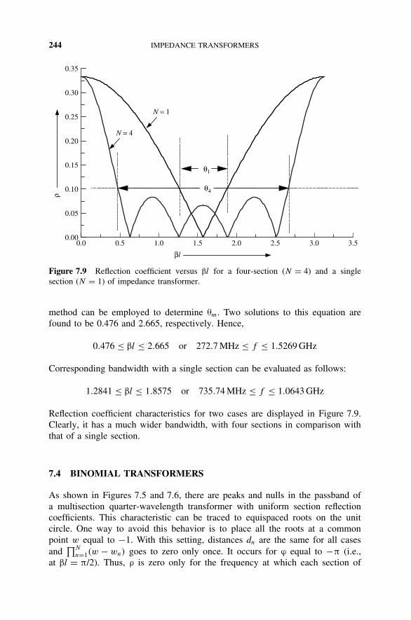
244 IMPEDANCE TRANSFORMERS
0.0 0.5 1.0 1.5 2.0 2.5 3.0 3.50.00
0.05
0.10
0.15
0.20
0.25
0.30
0.35
θ1
θ4
N = 4
N = 1
ρ
βl
Figure 7.9 Reflection coefficient versus βl for a four-section (N = 4) and a singlesection (N = 1) of impedance transformer.
method can be employed to determine θm. Two solutions to this equation arefound to be 0.476 and 2.665, respectively. Hence,
0.476 ≤ βl ≤ 2.665 or 272.7 MHz ≤ f ≤ 1.5269 GHz
Corresponding bandwidth with a single section can be evaluated as follows:
1.2841 ≤ βl ≤ 1.8575 or 735.74 MHz ≤ f ≤ 1.0643 GHz
Reflection coefficient characteristics for two cases are displayed in Figure 7.9.Clearly, it has a much wider bandwidth, with four sections in comparison withthat of a single section.
7.4 BINOMIAL TRANSFORMERS
As shown in Figures 7.5 and 7.6, there are peaks and nulls in the passband ofa multisection quarter-wavelength transformer with uniform section reflectioncoefficients. This characteristic can be traced to equispaced roots on the unitcircle. One way to avoid this behavior is to place all the roots at a commonpoint w equal to −1. With this setting, distances dn are the same for all casesand
∏Nn=1(w − wn) goes to zero only once. It occurs for ϕ equal to −π (i.e.,
at βl = π/2). Thus, ρ is zero only for the frequency at which each section of

BINOMIAL TRANSFORMERS 245
the transformer is λ/4 long. With wn = −1 for all n, equation (7.2.9) may bewritten as
N
=N∏
n=1
(w − wn) = (w + 1)N =N∑
m=0
N !
m!(N − m)!wm (7.4.1)
The following binomial expansion is used in writing (7.4.1):
(1 + x)m =N∑
n=1
m!
n!(m − n)!xn
A comparison of equation (7.4.1) with (7.2.7) indicates that
n
N
= N !
n!(N − n)!n = 0, 1, 2, . . . , N (7.4.2)
and therefore the section reflection coefficients, normalized to N , are binomiallydistributed.
From equation (7.4.1),
= N(w + 1)N ⇒ (βl) = N(e−j2βl + 1)N = N2Ne−jNβl (cos βl)N
orρ(βl) = ρN2N | cos βl|N (7.4.3)
For βl = 0, load RL is effectively connected to the input line. Therefore,
ρ(0) = ρN2N =∣∣∣∣RL − Z0
RL + Z0
∣∣∣∣ (7.4.4)
and
ρ(βl) =∣∣∣∣RL − Z0
RL + Z0
∣∣∣∣ × | cos βl|N (7.4.5)
Reflection coefficient characteristics of multisection binomial transformers versusβl (in degrees) are illustrated in Figure 7.10. The reflection coefficient scale isnormalized with the load reflection coefficient ρL. Unlike the preceding case ofuniformly distributed section reflection coefficients, it shows a smooth character-istic without lobes.
Example 7.3 Design a four-section quarter-wavelength binomial impedancetransformer to match a 100- load to a 50- air-filled coaxial line at 900 MHz.Determine the range of frequencies over which the reflection coefficient remainsbelow 0.1. Compare this result with that obtained in Example 7.2.

246 IMPEDANCE TRANSFORMERS
N = 2
N = 20
N = 9N = 6
N = 1
0 45 90 135 180
θ (deg)
0.0
0.2
0.4
0.6
0.8
1.0
Ref
lect
ion
coef
fici
ent
Figure 7.10 Reflection coefficient versus βl for a multisection binomial transformer.
SOLUTION With N = 4 and n = 0, 1, and 2 in (7.4.2), we get
0
4= 4!
0!4!= 4
4⇒ 0 = 4
1
4= 4!
1!3!= 3
4⇒ 1 = 3 = 44
and2
4= 4!
2!2!= 6 ⇒ 2 = 64
From (7.4.4),
ρ(0) = ρN2N =∣∣∣∣RL − Z0
RL + Z0
∣∣∣∣ ⇒ ρ4 = 1
24
∣∣∣∣100 − 50
100 + 50
∣∣∣∣ = 1
48= 0.020833
and from (7.2.8),
n = Zn+1 − Zn
Zn+1 + Zn
⇒ ρn(Zn+1 + Zn) = Zn+1 − Zn
Therefore,
Zn = 1 − ρn
1 + ρn
× Zn+1 (7.4.6)
Alternatively,
Zn+1 = 1 + ρn
1 − ρn
× Zn (7.4.7)

BINOMIAL TRANSFORMERS 247
Characteristic impedance of each section can be determined from (7.4.6), asfollows:
Z4 = 1 − 1/48
1 + 1/48× 100 = 95.9184
Z3 = 1 − 4/48
1 + 4/48× 95.9184 = 81.1617
Z2 = 1 − 6/48
1 + 6/48× 81.1617 = 63.1258
and
Z1 = 1 − 4/48
1 + 4/48× 63.1258 = 53.4141
If we continue with this formula, we find that
Z0 = 1 − 1/48
1 + 1/48× 53.4141 = 51.2339
This is different from the given value of 50 . It happened because of the approx-imation involved in the formula. Error keeps building up if the characteristicimpedances are determined proceeding in just one way. To minimize it, commonpractice is to determine the characteristic impedances up to halfway proceedingfrom the load side and then the remaining half from the input side. Thus, Z1 andZ2 should be determined from (7.4.7) as follows:
Z1 = 1 + 1/48
1 − 1/48× 50 = 52.1277
and
Z2 = 1 + 4/48
1 − 4/48× 50 = 61.6054
The frequency range over which the reflection coefficient remains below 0.1 canbe determined from (7.4.5) as follows:
0.1 = 13 | cos(ϑM)|4 ⇒ ϑM = 0.7376
Therefore,
0.7376 ≤ βl ≤ 2.404 or 422.61 MHz ≤ f ≤ 1.3774 GHz
Clearly, it has a larger frequency bandwidth than that of a single section. How-ever, it is less than the bandwidth obtained with uniformly distributed sectionreflection coefficients. Reflection coefficient as a function of βl is illustrated inFigure 7.11.

248 IMPEDANCE TRANSFORMERS
0.0 0.5 1.0 1.5 2.0 2.5 3.0 3.50.00
0.05
0.10
0.15
0.20
0.25
0.30
0.35
βl
ρ(βl
) θB
Figure 7.11 Reflection coefficient of a four-section binomial transformer versus βl.
7.5 CHEBYSHEV TRANSFORMERS
Consider again the case of a uniform three-section impedance transformer thatis connected between a 50- line and 100- load. Distribution of zeros aroundthe unit circle is shown in Figure 7.12 with solid points. Its frequency responseis illustrated in Figure 7.13 as curve (a). Now, let us move two of these zeros to±120 while keeping the remaining one fixed at 180, as illustrated by unfilled
Real w
Imaginary w
Figure 7.12 Distribution of zeros for a uniform three-section impedance transformer(solid), with two of those zeros moved to ±120 (unfilled) or to ±60 (hatched).

CHEBYSHEV TRANSFORMERS 249
0 1 2 3 4 5 6
0.5
0.4
0.3
0.2
0.1
0
(a)
(b)(c)
ρ(ϕ)
ϕ
Figure 7.13 Reflection coefficient versus ϕ for (a) a uniform three-section transformer,(b) two zeros moved to ±120, and (c) two zeros moved to ±60.
points in Figure 7.12. With this change in the distribution of zeros on the complexw-plane, ρ(βl) versus βl varies as shown by curve (b) in Figure 7.13. It showsrelatively much lower peaks of intervening lobes, while the widths and heightsof the two main lobes increase. On the other hand, if we move the two zeros to±60, the main peaks go down while intervening lobes rise. This is illustratedby hatched points in Figure 7.12 and by curve (c) in Figure 7.13. In this case,minor lobes increase while the main lobes are reduced in size. Note that zeros inthis case are uniformly distributed around the unit circle, and therefore its ρ(βl)
characteristic has identical lobes.Thus, the heights of intervening lobes decrease at the cost of the main lobe
when zeros are moved closer together. On the other hand, moving the zeros fartherapart raises the level of intervening lobes but reduces the main lobe. However, weneed a systematic method to determine the location of each zero for a maximumpermissible reflection coefficient, ρM , and the number of quarter-wave sections,N . An optimal distribution of zeros around the unit circle will keep the peaks ofall passband lobes at the same height of ρM .
In order to have the magnitudes of all minor lobes in the passband equal,section reflection coefficients are determined by the characteristics of Chebyshevfunctions, named after the Russian mathematician who first studied them. Thesefunctions satisfy the following differential equation:
(1 − x2)d2Tm(x)
dx2− x
dTm(x)
dx+ m2Tm(x) = 0 (7.5.1)
Chebyshev functions of degree m, represented by Tm(x), are mth-degree poly-nomials that satisfy (7.5.1). The first four of these and a recurrence relation for
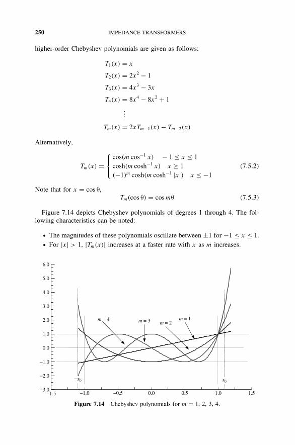
250 IMPEDANCE TRANSFORMERS
higher-order Chebyshev polynomials are given as follows:
T1(x) = x
T2(x) = 2x2 − 1
T3(x) = 4x3 − 3x
T4(x) = 8x4 − 8x2 + 1
...
Tm(x) = 2xTm−1(x) − Tm−2(x)
Alternatively,
Tm(x) =
cos(m cos−1 x) − 1 ≤ x ≤ 1cosh(m cosh−1 x) x ≥ 1(−1)m cosh(m cosh−1 |x|) x ≤ −1
(7.5.2)
Note that for x = cos θ,Tm(cos θ) = cos mθ (7.5.3)
Figure 7.14 depicts Chebyshev polynomials of degrees 1 through 4. The fol-lowing characteristics can be noted:
ž The magnitudes of these polynomials oscillate between ±1 for −1 ≤ x ≤ 1.ž For |x| > 1, |Tm(x)| increases at a faster rate with x as m increases.
−3.0
−2.0
−1.0
0.0
1.0
2.0
3.0
4.0
5.0
6.0
−1.5 −1.0 −0.5 0.0 0.5 1.0 1.5
m = 3m = 4m = 2
m = 1
−x0 x0
Figure 7.14 Chebyshev polynomials for m = 1, 2, 3, 4.

CHEBYSHEV TRANSFORMERS 251
ž The numbers of zeros are equal to the order of the polynomials. Zeros ofan even-order polynomial are located symmetrically about the origin, withone of the minor lobes’ peak at x = 0.
ž Polynomials of odd orders have one zero at x = 0 while the remaining zerosare located symmetrically.
These characteristics of Chebyshev polynomials are utilized to design animpedance transformer that has ripples of equal magnitude in its passband. Thenumber of quarter-wave sections determines the order of Chebyshev polynomialsand the distribution of zeros on the complex w-plane is selected according to that.With x0 properly selected, |Tm(x)| corresponds precisely to ρ(βl). This is doneby linking βl to x of Chebyshev polynomial as follows:
x = x0 cos βl (7.5.4)
Consider the design of a three-section equal-ripple impedance transformer.A Chebyshev polynomial of order 3 is appropriate for this case. Figure 7.15illustrates T3(x) together with (7.5.4). It is to be noted that Chebyshev variable x
and angle ϕ on the complex w-plane are related through (7.5.4) because ϕ is equalto −2βl. As ϕ varies from 0 to −2π, x changes as illustrated in Figure 7.15(b)and the corresponding T3(x) in Figure 7.15(a). Figure 7.16 shows |T3(ϕ)|, whichcan represent the desired ρ(ϕ) provided that
T3(ϕ = 0)
1= T3(x0)
1=
∣∣∣∣ (RL − Z0)
(RL + Z0)
∣∣∣∣ρM
(7.5.5)
where ρM is the maximum allowed reflection coefficient in the passband.For an m-section impedance transformer, (7.5.5) can be written as
Tm(x0) =∣∣∣∣RL − Z0
RL + Z0
∣∣∣∣ 1
ρM
(7.5.6)
Location x0 can now be determined from (7.5.2) as follows:
x0 = cosh
[1
m× cosh−1 Tm(x0)
](7.5.7)
With x0 determined from (7.5.7), |Tm(x)| represents the ρ(βl) desired. Hence,zeros of the reflection coefficient are the same as those of Tm(x). Since Chebyshevpolynomials have zeros in the range −1 < x < 1, zeros of ρ(ϕ) can be determinedfrom (7.5.2). Therefore,
Tm(xn) = 0 ⇒ cos(m × cos−1 xn) = 0 = ± cos[(2n − 1)
π
2
]n = 1, 2, . . .

252 IMPEDANCE TRANSFORMERS
−1.5 −1.0 −0.5 0.0 0.5 1.0 1.5
−2.0
0.0
2.0
x0 cos βl
(a)
(b)0
βl
π
Figure 7.15 Third-order Chebyshev polynomial (a) and its variable, x versus βl (b).
−7.0 −6.0 −5.0 −4.0 −3.0 −2.0 −1.0 0.00.0
0.5
1.0
2.0
2.5
1.5
T3(x0)RL − Z0RL + Z0
ρM
Figure 7.16 |T3(x)| versus ϕ and its relationship with the desired ρ(ϕ).
where xn is the location of the nth zero. Hence,
xn = ± cos[(2n − 1)
π
2m
](7.5.8)
and the corresponding ϕn can be evaluated from (7.5.4) as follows:
ϕn = 2 cos−1 xn
x0(7.5.9)

CHEBYSHEV TRANSFORMERS 253
The zeros of ρ(ϕ), wn, on the complex w-plane are now known becausewn = eiϕn . Equation (7.2.9) can be used to determine the section reflection coef-ficient, n. Zn is, in turn, determined from equation (7.2.8). The bandwidth ofthe impedance transformer extends from x = −1 to x = +1. With βl = θM atx = 1, (7.5.4) gives
cos θM = 1
x0
Therefore, bandwidth of a Chebyshev transformer can be expressed as follows:
cos−1 1
x0≤ βl ≤ π − cos−1 1
x0(7.5.10)
Example 7.4 Reconsider the matching of a 100- load to a 50- line. Designan equal-ripple four-section quarter-wavelength impedance transformer and com-pare its bandwidth with those obtained earlier for ρM = 0.1.
SOLUTION From (7.5.6),
T4(x0) =∣∣∣∣100 − 50
100 + 50
∣∣∣∣ × 1
0.1= 1
0.3= 3.3333
Therefore, x0 can now be determined from (7.5.7) as follows:
x0 = cosh[
14 cosh−1(3.3333)
]In case inverse hyperbolic functions are not available on a calculator, the follow-ing procedure can be used to evaluate x0. Assume that y = cosh−1(3.3333) ⇒3.3333 = cosh y = (ey + e−y)/2.
Hence,ey + e−y = 2 × 3.3333 = 6.6666
or
e2y − 6.6666 × ey + 1 = 0 ⇒ ey = 6.6666 ± √(6.6666)2 − 4
2= 6.5131
and0.1535y = ln(6.5131) = 1.8738
Therefore,1
4cosh−1(3.3333) = 1.8738
4= 0.4684
and
x0 = cosh(0.4684) = e0.4684 + e−0.4684
2= 1.1117
Note that the other solution of ey produces y = −1.874 and x0 = 1.1117.
254 IMPEDANCE TRANSFORMERS
From (7.5.8) and (7.5.9), we get
xn = ±0.9239, ±0.3827
andϕn = −67.61
,−139.71, −220.29
, −292.39
Therefore,
w1 = 0.381 − j0.925
w2 = −0.763 − j0.647
w3 = −0.763 + j0.647
and
w4 = 0.381 + j0.925
Now, from equation (7.2.9) we get
= 4(1 + 0.764w + 0.837w2 + 0.764w3 + w4)
Therefore,
0 = 4, 1 = 3 = 0.7644 and 2 = 0.8374
From equation (7.2.12), we have
=N∑
n=0
n = RL − Z0
RL + Z0⇒ 4.3654 = RL − Z0
RL + Z0
4 = 1
4.365× 100 − 50
100 + 50= 0.076
Hence,
0 = 4 = 0.076, 1 = 3 = 0.058, and 2 = 0.064
Now, the characteristic impedance of each section can be determined from(7.2.8) as follows:
4 = ZL − Z4
ZL + Z4⇒ Z4 = 1 − 4
1 + 4ZL = 85.87
3 = Z4 − Z3
Z4 + Z3⇒ Z3 = 1 − 3
1 + 3Z4 = 76.46
2 = Z3 − Z2
Z3 + Z2⇒ Z2 = 1 − 2
1 + 2Z3 = 67.26

EXACT ANALYSIS OF MULTISECTION TRANSFORMERS 255
and
1 = Z2 − Z1
Z2 + Z1⇒ Z1 = 1 − 1
1 + 1Z2 = 59.89
To minimize the accumulating error in Zn, it is advisable to calculate half ofthe impedance values from the load side and the other half from the input side.In other words, Z1 and Z2 should be determined as follows:
Z1 = 1 + 0
1 − 0Z0 = 58.2251
and
Z2 = 1 + 1
1 − 1Z1 = 65.3951
The bandwidth is determined from (7.5.10) as follows:
cos βl = 1
x0= 0.899 ⇒ βl = 0.452
Therefore,0.452 ≤ βl ≤ 2.6896
Thus, the bandwidth is greater than what was achieved from either a uniform ora binomial distribution of n coefficients.
7.6 EXACT FORMULATION AND DESIGN OF MULTISECTIONIMPEDANCE TRANSFORMERS
The analysis and design presented so far is based on the assumption that thesection reflection coefficients are small, as implied by (7.2.5). If this is not thecase, an exact expression for the reflection coefficient must be used. Alternatively,there are design tables available in the literature (e.g., Matthaei et al., 1980) thatcan be used to synthesize an impedance transformer. In case of a two- or three-section Chebyshev transformer, the design procedure summarized below may beused as well.
Exact formulation of the multisection impedance transformer is convenientlydeveloped via the power loss ratio, PLR, defined as follows:
PLR = incident power
power delivered to the load
If Pin represents the incident power and ρin is the input reflection coefficient, then
PLR = Pin
(1 − ρ2in)Pin
= 1
1 − ρ2in
⇒ ρin =√
PLR − 1
PLR(7.6.1)
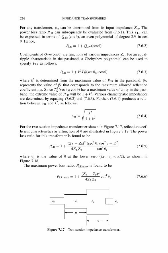
256 IMPEDANCE TRANSFORMERS
For any transformer, ρin can be determined from its input impedance Zin. Thepower loss ratio PLR can subsequently be evaluated from (7.6.1). This PLR canbe expressed in terms of Q2N(cos θ), an even polynomial of degree 2N in cosθ. Hence,
PLR = 1 + Q2N(cos θ) (7.6.2)
Coefficients of Q2N(cos θ) are functions of various impedances Zn. For an equal-ripple characteristic in the passband, a Chebyshev polynomial can be used tospecify PLR as follows:
PLR = 1 + k2T 2N(sec θM cos θ) (7.6.3)
where k2 is determined from the maximum value of PLR in the passband. θM
represents the value of βl that corresponds to the maximum allowed reflectioncoefficient ρM . Since T 2
N(sec θM cos θ) has a maximum value of unity in the pass-band, the extreme value of PLR will be 1 + k2. Various characteristic impedancesare determined by equating (7.6.2) and (7.6.3). Further, (7.6.1) produces a rela-tion between ρM and k2, as follows:
ρM =√
k2
1 + k2(7.6.4)
For the two-section impedance transformer shown in Figure 7.17, reflection coef-ficient characteristics as a function of θ are illustrated in Figure 7.18. The powerloss ratio for this transformer is found to be
PLR = 1 + (ZL − Z0)2
4ZLZ0
(sec2 θz cos2 θ − 1)2
tan4 θz
(7.6.5)
where θz is the value of θ at the lower zero (i.e., θz < π/2), as shown inFigure 7.18.
The maximum power loss ratio, PLR max, is found to be
PLR max = 1 + (ZL − Z0)2
4ZLZ0cot4 θz (7.6.6)
ZLZ2Z1Z0
θ
θ
Figure 7.17 Two-section impedance transformer.

EXACT ANALYSIS OF MULTISECTION TRANSFORMERS 257
θM θZ
ρM
|Γin |
π/2 π − θM
θ
Figure 7.18 Reflection coefficient characteristics of a two-section Chebyshev trans-former.
Hence,
k2 = (ZL − Z0)2
4ZLZ0cot4 θz (7.6.7)
Required values of characteristic impedances, Z1 and Z2, are determined fromthe equations
Z21 = Z2
0
[(ZL − Z0)
2
4Z20 tan4 θz
+ ZL
Z0
]1/2
+ (ZL − Z0)Z0
2 tan2 θz
(7.6.8)
and
Z2 = ZL
Z1Z0 (7.6.9)
The passband edge, θM , is given by
θM = cos−1(√
2 cos θz) (7.6.10)
Hence, the bandwidth of this transformer is found as
θM ≤ θ = βl ≤ π − θM (7.6.11a)

258 IMPEDANCE TRANSFORMERS
For a TEM wave,f
f0= 2 − 4θM
π(7.6.11b)
If the bandwidth is specified in a design problem along with ZL and Z0,then θM is known. Therefore, θz can be determined from (7.6.10). ImpedancesZ1 and Z2 are determined subsequently from (7.6.8) and (7.6.9), respectively.The corresponding maximum reflection coefficient ρM can easily be evaluatedfollowing k2 from (7.6.7). On the other hand, if ρM is specified instead of θM , thenk2 is determined from (7.6.4). θz, in turn, is calculated from (7.6.7). Now, Z1,Z2, and θM can be determined from (7.6.8), (7.6.9), and (7.6.10), respectively.
In the limit θz → π/2, two zeros of ρ in Figure 7.18 come together to give amaximally flat transformer. In that case, (7.6.8) and (7.6.9) are simplified to give
Z1 = Z1/4L × Z
3/40 (7.6.12)
Z2 = Z3/4L × Z
1/40 (7.6.13)
and
θM = cos−1(cot θz) (7.6.14)
Example 7.5 Use the exact theory to design a two-section Chebyshev trans-former to match a 500- load to a 100- line. The required fractional bandwidthis 0.6. What is the resulting value of ρM?
SOLUTION From (7.6.10) and (7.6.11),
f
f0= 2 − 4
πcos−1(
√2 cos θz) ⇒ cos θz = 1√
2cos
(2 − f/f0
4/π
)
= 1√2
cos
(2 − 0.6
4/π
)= 0.321
Therefore, θz = 1.244 rad and
θM = cos−1(√
2 cos θz) = cos−1(√
2 × 0.321) = 1.1
From (7.6.7),
k2 = (ZL − Z0)2
4ZLZ0cot4 θz = (ZL − 1)2
4ZL
cot4 θz = 0.0106
Therefore, from (7.6.4),
ρM =√
k2
1 + k2= 0.1022
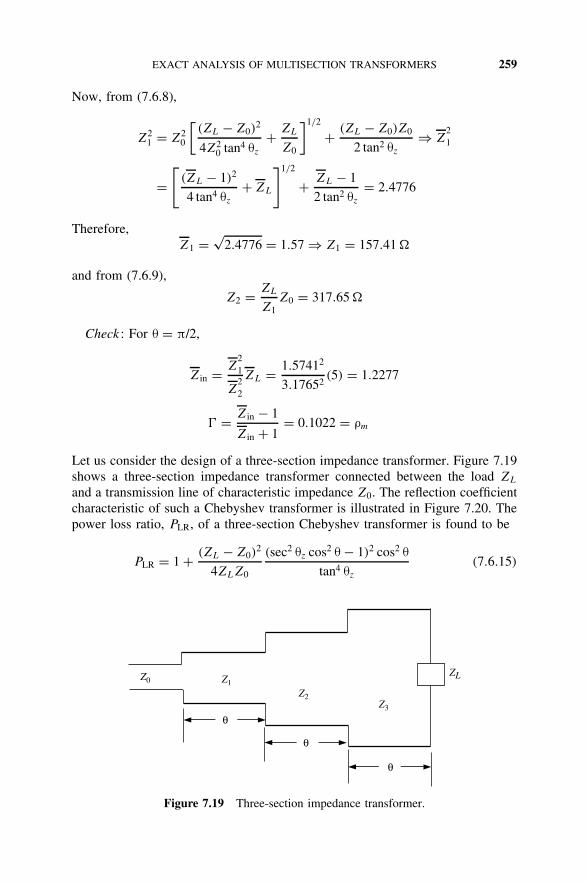
EXACT ANALYSIS OF MULTISECTION TRANSFORMERS 259
Now, from (7.6.8),
Z21 = Z2
0
[(ZL − Z0)
2
4Z20 tan4 θz
+ ZL
Z0
]1/2
+ (ZL − Z0)Z0
2 tan2 θz
⇒ Z21
=[
(ZL − 1)2
4 tan4 θz
+ ZL
]1/2
+ ZL − 1
2 tan2 θz
= 2.4776
Therefore,Z1 = √
2.4776 = 1.57 ⇒ Z1 = 157.41
and from (7.6.9),
Z2 = ZL
Z1Z0 = 317.65
Check : For θ = π/2,
Zin = Z21
Z22
ZL = 1.57412
3.17652(5) = 1.2277
= Zin − 1
Zin + 1= 0.1022 = ρm
Let us consider the design of a three-section impedance transformer. Figure 7.19shows a three-section impedance transformer connected between the load ZL
and a transmission line of characteristic impedance Z0. The reflection coefficientcharacteristic of such a Chebyshev transformer is illustrated in Figure 7.20. Thepower loss ratio, PLR, of a three-section Chebyshev transformer is found to be
PLR = 1 + (ZL − Z0)2
4ZLZ0
(sec2 θz cos2 θ − 1)2 cos2 θ
tan4 θz
(7.6.15)
ZL
Z2
Z1Z0
Z3
θ
θ
θ
Figure 7.19 Three-section impedance transformer.

260 IMPEDANCE TRANSFORMERS
θM θZ
θρM
Γin ||
Figure 7.20 Reflection coefficient characteristics of a three-section Chebyshev trans-former.
It attains the maximum allowed value at θ = θM , where
θM = cos−1
(2√3
cos θz
)(7.6.16)
Since the maximum power loss ratio must be equal to 1 + k2,
k2 = (ZL − Z0)2
4ZLZ0
(2 cos θz
3√
3 tan2 θz
)2
(7.6.17)
Characteristic impedance Z1 is obtained by solving the equation
ZL − Z0
tan2 θz
= Z21
Z0+ 2
(ZL
Z0
)1/2
Z1 − ZLZ20
Z21
− 2
(ZL
Z0
)1/2
Z−11 Z2
0 (7.6.18)
The other two characteristic impedances, Z2 and Z3, are then determined asfollows:
Z2 = √ZLZ0 (7.6.19)
and
Z3 = ZLZ0
Z1(7.6.20)
EXACT ANALYSIS OF MULTISECTION TRANSFORMERS 261
The range of the passband (bandwidth) is still given by (7.6.11) provided thatθM is now computed from (7.6.16).
Example 7.6 Design a three-section Chebyshev transformer (exact theory) tomatch a 500- load to a 100- line. The required fractional bandwidth is 0.6.Compute ρM and compare it with that obtained in Example 7.5.
SOLUTION From (7.6.16) and (7.6.11),
θM = cos−1
(2√3
cos θz
)and
f
f0= 0.6 ⇒ (π/2) − θM
π/2
= 0.3 ⇒ θM = π
2(1 − 0.3) = 1.1
Therefore,
cos θz =√
3
2cos θM = 0.3932 ⇒ θz = 1.17 rad
Now, from (7.6.17),
k2 = (ZL − Z0)2
4ZLZ0
(2 cos θz
3√
3 tan2 θz
)2
= (ZL − 1)2
4ZL
(2 cos θz
3√
3 tan2 θz
)2
= 6.125 × 10⁻⁴
and from (7.6.4),
ρM =√
k2
1 + k2= 0.0247
which is approximately one-fourth of the previous (two-section transformer) case.Z1 is obtained by solving equation (7.6.18) as follows:
ZL − Z0
tan2 θz
= Z21
Z0+ 2
(ZL
Z0
)1/2
Z1 − ZLZ20
Z21
− 2
(ZL
Z0
)1/2
Z−11 Z2
0
or
ZL − 1
tan2 θz
= Z21 + 2(ZL)1/2 Z1 − ZL
Z21
− 2(ZL)1/2 Z−11 = 4
tan2 θz
= 0.7314
Therefore,
Z21 + 2
√5 Z1 − 5
Z21
− 2√
5
Z1= 0.7314
orZ
41 + 2
√5 Z
31 − 0.7314 Z
21 − 2
√5 Z1 − 5 = 0
262 IMPEDANCE TRANSFORMERS
Therefore,
Z1 = −4.4679, (−0.6392 − j0.6854), (−0.6392 + j0.6854), and 1.2741
Thus, only one of these solutions can be physically realized because the othershave a negative real part. After selecting Z1 = 127.42 , (7.6.19) and (7.6.20)give
Z3 = ZLZ0
Z1= 392.4277
and
Z2 = √ZLZ0 = 223.6068
If we use the approximate formulation, then following the procedure of Example7.4, we find from (7.5.6) that
T3(x0) = 500 − 100
500 + 100× 1
0.02474= 26.9458
Now, from (7.5.7),
x0 = cosh[ 13 cosh−1(26.9458)] = 2.0208
and from (7.5.8),
xn = ± cos[(2n − 1)
π
6
]= ±0.866, 0
Using (7.5.9) we get
ϕn = 2.2558, 3.1416, and 4.0274
Since wn = ejϕn , we find that
w1 = −0.6327 + j0.7744
w2 = −0.6327 − j0.7744
w3 = −1
and from (7.2.9),
3= (w − w1)(w − w2)(w − w3) = w3 + 2.2654w2 + 2.2654w + 1
Hence,
0 = 3
1 = 2 = 2.26543
TAPERED TRANSMISSION LINES 263
Now, from (7.2.12),
0 + 1 + 2 + 3 = 6.53073 = 500 − 100
500 + 100
Therefore,3 = 0.1021 = 0
1 = 2 = 0.2313
Corresponding impedances are now determined from (7.2.8) as follows:
Z1 = 1 + 0
1 − 0= 1.2274
Z2 = 1 + 1
1 − 1Z1 = 2.4234
calculated from the input side
and
Z3 = 1 − 3
1 + 3ZL = 4.0737 calculated from the load side
A comparison of these values with those obtained earlier using the exact for-mulation shows that the two sets are within 10% of deviation for this example.Note that for the fractional bandwidth of 0.6 with a single section, reflectioncoefficient ρM increases to 0.3762.
7.7 TAPERED TRANSMISSION LINES
Consider that the multisection impedance transformer of Figure 7.4 is replaced bya tapered transition of length L, as illustrated in Figure 7.21. The characteristicimpedance of this transition is a continuous smooth function of distance, withits values at the two ends as Z0 and RL. An approximate theory of such amatching section can easily be developed on the basis of the analysis presentedin Section 7.2.
The continuously tapered line can be modeled by a large number of incrementalsections of length δz. One of these sections, connected at z, has a characteristicimpedance of Z + δZ, and the one before it has a characteristic impedance of Z,as shown in Figure 7.21. These impedance values are conveniently normalizedby Z0 before obtaining the incremental reflection coefficient at distance z. Hence,
δ0 = Z + δZ − Z
Z + δZ + Z≈ δZ
2Z(7.7.1)
As δz → 0, it can be written as
d0 = dZ
2Z= 1
2
d(ln Z)
dzdz (7.7.2)

264 IMPEDANCE TRANSFORMERS
L
zZ0
Z Z + δZ
δzRL
Figure 7.21 Tapered transition connected between load RL and transmission line ofcharacteristic impedance Z0.
The corresponding incremental reflection coefficient din at the input can bewritten as follows:
din ≈ e−j2βzd0 = e−j2βz
(1
2
)d
dz(ln Z) dz
The total reflection coefficient, in, at the input of the tapered section can bedetermined by summing up these incremental reflections with their appropriatephase angles. Hence,
in =∫ L
0din = 1
2
∫ L
0e−j2βz d
dz(ln Z) dz (7.7.3)
Therefore, in can be determined from (7.7.3) provided that Z(z) is given. How-ever, the synthesis problem is a bit complex because in that case, Z(z) is to bedetermined for a specified in. Let us first consider a few examples of evaluatingin for the given distributions of d(ln Z)/dz.
Case 1d
dz(ln Z) is constant over the entire length of the taper. Suppose that
d
dzln Z(z) = C1 0 ≤ z ≤ L
where C1 is a constant. On integrating this equation, we get
ln Z(z) = C1z + C2
With Z(z = 0) = 1 and Z(z = L) = RL, constants C1 and C2 can be determined.Hence,
ln Z = z
Lln RL ⇒ Z = e(z/L) ln RL (7.7.4)

TAPERED TRANSMISSION LINES 265
Thus, the impedance is changing exponentially with distance. Therefore, thiskind of taper is called an exponential taper. From (7.7.3), the total reflectioncoefficient is found as
in = 1
2
∫ L
0e−j2βz d
dz
( z
Lln RL
)dz = ln RL
2L
∫ L
0e−j2βz dz = ln RL
2L
e−j2βz
−j2β
∣∣∣∣L
0
or
in = ln RL
2L
e−jβL − 1
−j2β= ln RL
2e−jβL sin βL
βL⇒ 2ρin
ln RL
= sin βL
βL(7.7.5)
where ρin = |in|. It is assumed in this evaluation that β = 2π/λ is not changingwith distance z. The right-hand side of (7.7.5) is displayed in Figure 7.22 as afunction of βL. Since L is fixed for a given taper and β is related directly tosignal frequency, this plot also represents the frequency response of an exponen-tial taper.
Case 2d
dz(ln Z) is a triangular function. If
d
dz(ln Z) is a triangular function,
defined as
d(ln Z)
dz=
4z
L2ln RL 0 ≤ z ≤ L
2
4
(1
L− z
L2
)ln RL
L
2≤ z ≤ L
(7.7.6)
0.0000 3.1416 6.2832 9.4248 12.5664 15.7080 18.8496 21.99120.0
0.2
0.4
0.6
0.8
1.0
βL
Figure 7.22 Frequency response of an exponential taper.

266 IMPEDANCE TRANSFORMERS
then
ln Z =
∫ L/20
4z
L2ln RL dz 0 ≤ z ≤ L
2∫ L
L/2 4
(1
L− z
L2
)ln RL dz
L
2≤ z ≤ L
or
ln Z =
2z2
L2ln RL + c1 0 ≤ z ≤ L
2
4
(z
L− z2
2L2
)ln RL + c2
L
2≤ z ≤ L
Integration constants c1 and c2 are determined from the given conditions Z(z =0) = 1 and Z(z = L) = RL. Hence,
Z =
exp
2z2
L2ln RL
0 ≤ z ≤ L
2
exp
(4z
L− 2z2
L2− 1
)ln RL
L
2≤ z ≤ L
(7.7.7)
and therefore total reflection coefficient is found from (7.7.3) as
in = 1
2
[∫ L/2
0e−j2βz 4z
L2ln RL dz +
∫ L
L/2e−j2βz 4
L2(L − z) ln RL dz
]or
in = 2 ln RL
L2
[∫ L/2
0ze−j2βz dz +
∫ L
L/2(L − z)e−j2βz dz
]
Since ∫ze−j2βz dz = ze−j2βz
−j2β− e−j2βz
(−j2β)2
and ∫e−j2βz dz = e−j2βz
−j2β
in can be found as follows:
in = 1
2e−jβL ln RL
[sin(βL/2)
βL/2
]2
(7.7.8)
Figure 7.23 shows normalized magnitude of in as a function of βL. As before,it also represents the frequency response of this taper of length L. When wecompare it with that of Figure 7.22 for an exponential taper, we find that the

TAPERED TRANSMISSION LINES 267
0.0
0.2
0.4
0.6
0.8
1.0
0.0000 3.1416 6.2832 9.4248 12.5664 15.7080 18.8496 21.9912
βL
Figure 7.23 Frequency response of a taper with triangular distribution.
magnitude of minor lobes is reduced now, but the main lobe has become relativelywider. It affects the cutoff frequency of a given taper. For example, if the maxi-mum allowed normalized reflection coefficient is 0.2, an exponential taper has alower value of βL than that of a taper with triangular distribution. However, it isthe other way around for a normalized reflection coefficient of 0.05. For a fixedlength L, βL is proportional to frequency, and hence the lower value of βL hasa lower cutoff frequency than in the other case.
Figure 7.24 depicts variation in normalized characteristic impedance along thelength of two tapers. A coaxial line operating in the TEM mode can be used todesign these tapers by varying the diameter of its inner conductor. Similarly, thenarrow sidewall width of a TE10-mode rectangular waveguide can be modifiedto get the desired taper while keeping its wide side constant.
Case 3d
dz(ln Z) is a Gaussian distribution. Assume that
d
dz(ln Z) = K1e
−α(z−L/2)2(7.7.9)
This distribution is centered around the midpoint of the tapered section. Its fall-offrate is governed by the coefficient α. Integrating it over distance z, we find that
ln Z = K1
∫ z
0e−α(z′−L/2)2
dz′ (7.7.10)

268 IMPEDANCE TRANSFORMERS
0.0 0.2 0.4 0.6 0.8 1.01.0
1.2
1.4
1.6
1.8
2.0
(a)(b)
Figure 7.24 Distribution of normalized characteristic impedance along a tapered lineterminated by RL = 2Z0 for (a) case 1 and (b) case 2.
Since Z(z = L) = RL,
K1 = ln RL∫ L
0e−α(z′−L/2)2
dz′(7.7.11)
Therefore,
ln Z = ln RL
∫ z
0e−α(z′−L/2)2
dz′
∫ L
0e−α(z′−L/2)2
dz′(7.7.12)
and
in = 1
2K1
∫ L
0e−j2βze−α(z−L/2)2
dz (7.7.13)
With the following substitution of variable and associated limits of integrationin (7.7.11) and (7.7.13),
z − L
2= x
dz = dx
z = 0 → x = −L
2

TAPERED TRANSMISSION LINES 269
and
z = L → x = L
2
we get
in = 1
2K1
∫ L/2
−L/2e−j2β(x+L/2)e−αx2
dx = 1
2K1e
−jβL
∫ L/2
−L/2e−j2βxe−αx2
dx
or
in = 1
2ln RL e−jβl
∫ L/2
−L/2e−j2βxe−αx2
dx
∫ L/2
−L/2e−αx2
dx
= 1
2ln RL e−jβl
∫ L/2
0cos 2βx e−αx2
dx∫ L/2
0e−αx2
dx
(7.7.14)
It can be arranged after substituting√
α x with y, and√
α(L/2) with ξ as follows:
in = 1
2ln RL e−jβl
∫ ξ
0cos[(βL/ξ)y]e−y2
dy∫ ξ
0e−y2
dy
(7.7.15)
Figure 7.25 shows the normalized magnitude of the reflection coefficient versusβL for two different values of ξ. It indicates that the main lobe becomes wider,and the level of minor lobes goes down as ξ is increased.
1
0.8
0.6
0.4
0.2
00 5 10 15 20
(a)
(b)
βL
Figure 7.25 Frequency response of a tapered line with a normal distribution of normal-ized characteristic impedance for (a) ξ = 0.3 and (b) ξ = 3.

270 IMPEDANCE TRANSFORMERS
7.8 SYNTHESIS OF TRANSMISSION LINE TAPERS
The frequency response of a transmission line taper can be determined easilyfrom (7.7.3). However, the inverse problem of determining its impedance vari-ation that provides the desired frequency response needs further consideration.To this end, assume that F(α) is the Fourier transform of a function f (x). Inother words,
F(α) =∫ ∞
−∞f (x)e−jαx dx (7.8.1)
and
f (x) = 1
2π
∫ ∞
−∞F(α)ejαx dα (7.8.2)
For convenience, we rewrite (7.7.3) as follows:
in(2β) =∫ L
0
[1
2
d
dz(ln Z)
]e−j2βz dz
If 12 d(ln Z)/dz = 0 for −∞ ≤ z < 0 and for z > L, it may be written as
in(2β) =∫ ∞
−∞1
2
d
dz(ln Z)e−j2βz dz (7.8.3)
A comparison of (7.8.3) with (7.8.1) indicates that in(2β) represents the Fouriertransform of 1
2 d[ln Z(z)]/dz. Hence, from (7.8.2),
1
2
d(ln Z)
dz= 1
2π
∫ ∞
−∞in(2β)ej2βx d(2β) (7.8.4)
This equation can be used to design a taper that will have the desired reflec-tion coefficient characteristics. However, only those in(2β) that have an inverseFourier transform limited to 0 ≤ z ≤ L (zero outside this range) can be realized.At this point, we can conveniently introduce the following normalized variables:
p = 2πz − (L/2)
L(7.8.5)
and
u = βL
π= 2L
λ(7.8.6)
Therefore,
z = L
2π(p + π)
and
dz = L
2πdp

SYNTHESIS OF TRANSMISSION LINE TAPERS 271
New integration limits are found as −π ≤ p ≤ π. Hence,
in(2β) = 1
2
∫ π
−π
e−j2β(L/2+Lp/2π) d
dp(ln Z)
dp
dz
L
2πdp
or
in(2β) = 1
2e−jβL
∫ π
−π
e−jup d
dp(ln Z) dp (7.8.7)
Now, if we define g(p) = d(ln Z)/dp and F(u) = ∫ π
−πe−jupg(p) dp, (7.8.7)
can be expressed as follows:
in(2β) = 12e−jβLF (u)
or
ρin(2β) = 12 |F(u)|
Further,F(u = 0) = ln ZL (7.8.8)
Thus, F(u) and g(p) form the Fourier transform pair. Therefore,
g(p) = 1
2π
∫ ∞
−∞ejupF(u) du =
nonzero for |p| < π
0 for |p| > π(7.8.9)
To satisfy the conditions embedded in writing (7.8.3), only those F(u) thatproduce g(p) as zero for |p| > π can be synthesized. Suitable restrictions onF(u) can be derived after expanding g(p) in a complex Fourier series as follows:
g(p) =
∞∑n=−∞
anejnp −π ≤ p ≤ π
0 |p| > π
(7.8.10)
Since g(p) is a real function, constants an = a∗−n. Therefore,
F(u) =∫ π
−π
e−jup
∞∑n=−∞
anejnp dp =
∞∑n=−∞
an
∫ π
−π
e−j (u−n)p dp =∞∑
n=−∞an
e−j (u−n)p
−j (u − n)
∣∣∣∣π
−π
or
F(u) =∞∑
n=−∞an
e−j (u−n)π − ej (u−n)π
−j (u − n)= 2π
∞∑n=−∞
an
sin π(u − n)
π(u − n)(7.8.11)
For u = m (an integer),
sin π(m − n)
π(m − n)=
1 for m = n
0 for m = n
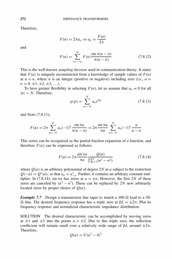
272 IMPEDANCE TRANSFORMERS
Therefore,
F(n) = 2πan ⇒ an = F(n)
2π
and
F(u) =∞∑
n=−∞F(n)
sin π(u − n)
π(u − n)(7.8.12)
This is the well-known sampling theorem used in communication theory. It statesthat F(u) is uniquely reconstructed from a knowledge of sample values of F(u)
at u = n, where n is an integer (positive or negative) including zero (i.e., u =n = 0, ±1,±2, ±3, . . .).
To have greater flexibility in selecting F(u), let us assume that an = 0 for all|n| > N . Therefore,
g(p) =N∑
n=−N
anejnp (7.8.13)
and from (7.8.11),
F(u) = 2π
N∑n=−N
an(−1)nsin πu
π(u − n)= 2π
sin πu
πu
N∑n=−N
an(−1)nu
u − n
This series can be recognized as the partial-fraction expansion of a function, andtherefore F(u) can be expressed as follows:
F(u) = 2πsin πu
πu
Q(u)∏Nn=1(u
2 − n2)(7.8.14)
where Q(u) is an arbitrary polynomial of degree 2N in u subject to the restrictionQ(−u) = Q∗(u), so that an = a∗−n. Further, it contains an arbitrary constant mul-tiplier. In (7.8.14), sin πu has zeros at u = ±n. However, the first 2N of thesezeros are canceled by (u2 − n2). These can be replaced by 2N new arbitrarilylocated zeros by proper choice of Q(u).
Example 7.7 Design a transmission line taper to match a 100- load to a 50- line. The desired frequency response has a triple zero at βL = ±2π. Plot itsfrequency response and normalized characteristic impedance distribution.
SOLUTION The desired characteristic can be accomplished by moving zerosat ±1 and ±3 into the points u = ±2. Due to this triple zero, the reflectioncoefficient will remain small over a relatively wide range of βL around ±2π.Therefore,
Q(u) = C(u2 − 4)3

SYNTHESIS OF TRANSMISSION LINE TAPERS 273
and
F(u) = 2πCsin πu
πu
(u2 − 4)3
(u2 − 1) × (u2 − 4) × (u2 − 9)
Since u = βL/π, F (u) versus u represents the frequency response of this taper.Further, it can be normalized with F (0) as follows:
∣∣∣∣F(u)
F (0)
∣∣∣∣ = 9
16
(sin πu
πu
)(u2 − 4)3
(u2 − 1)(u2 − 4)(u2 − 9)
A plot of this equation is illustrated in Figure 7.26. It shows that the normalizedmagnitude is very small around u = 2.
Since F (0) is given by (7.8.8), multiplying constant C in F(u) can be deter-mined easily. Hence,
F(0) = 2πC × 1 × (−4)3
(−1)(−4)(−9)= 2πC × 16
9= ln ZL ⇒ C = 9
32πln ZL
Further,
F(1) = 2πC
π
(sin πu
u2 − 1
)∣∣∣∣u=1
× (1 − 4)3
(1 − 4)(1 − 9)= Cπ
9
8
= 9
32πln ZL π
9
8= 0.3164 ln ZL
F(2) = 0
F(3) = 2πC
3π
(sin πu
u2 − 9
)∣∣∣∣u=3
× (9 − 4)3
(9 − 1)(9 − 4)= −25
72Cπ
=(
−25
72π
)× 9
32πln ZL = 0.09766 ln ZL
and F(n) = 0 for n > 3.Therefore,
a0 = 1
2πF(0) = 1
2πln ZL
a1 = a−1 = 1
2πF(1) = 0.3164
2πln ZL
a2 = a−2 = 0
a3 = a−3 = 1
2πF(3) = −0.09766
2πln ZL
and
an = a−n = 0 for n > 3

274 IMPEDANCE TRANSFORMERS
1
0.8
0.6
0.4
0.2
00 321 54 6
u
Figure 7.26 Normalized frequency response of the taper in Example 7.7.
Hence,
g(p) = d(ln Z)
dp= ln ZL
2π(a0 + 2a1 cos p + 2a3 cos 3p)
= ln ZL
2π(1 + 0.6328 × cos p − 0.1953 × cos 3p)
and
ln Z = ln ZL
2π(p + 0.6328 × sin p − 0.0651 × sin 3p) + c1
The integration constant c1 can be evaluated as follows:
ln Z = 0 at p = −π or ln Z = ln ZL at p = π
Therefore,c1 = 0.5 ln ZL
and
ln Z = ln ZL
2π(p + π + 0.6328 sin p − 0.0651 sin 3p)
where
p = 2π
L
(z − L
2
)
Normalized impedance (Z) versus the length of the taper (z/L) is illustrated inFigure 7.27.

SYNTHESIS OF TRANSMISSION LINE TAPERS 275
0.0 0.2 0.4 0.6 0.8 1.0
z/L
0.8
1.0
1.2
1.4
1.6
1.8
2.0
Nor
mal
ized
impe
danc
e
Figure 7.27 Normalized characteristic impedance variation along the length of the taperin Example 7.7.
Example 7.8 Design a taper to match a 100- load to a 50- transmission line.Its reflection coefficient has double zeros at βL = ±2π and ±3π. Plot its fre-quency response and normalized characteristic impedance versus the normalizedlength of the taper.
SOLUTION This design can be achieved by moving the zeros at u = ± 1 and± 4 into the points ± 2 and ± 3, respectively. Hence,
Q(u) = C(u2 − 22)2(u2 − 32)2 = C(u2 − 4)2(u2 − 9)2
and
F(u) = Csin πu
πu
(u2 − 4)2(u2 − 9)2
(u2 − 1)(u2 − 4)(u2 − 9)(u2 − 16)
Therefore, F (0) = 2.25C, F (1) = 0.8C, F (2) = 0, F (3) = 0, F (4) = (7/40)C,and F(n) = 0 for n > 4. From (7.8.8),
F(0) = ln ZL ⇒ C = ln ZL
2.25
and
g(p) = d(ln Z)
dp=
∞∑n=−∞
ane−jnp an = F(n)
2π
or
g(p) = 2.25C
2π+ 0.8C
2π(ejp + e−jp) + 7C
(40)(2π)(ej4p + e−j4p)
= ln ZL
2π(1 + 0.7111 cos p + 0.1556 cos 4p)
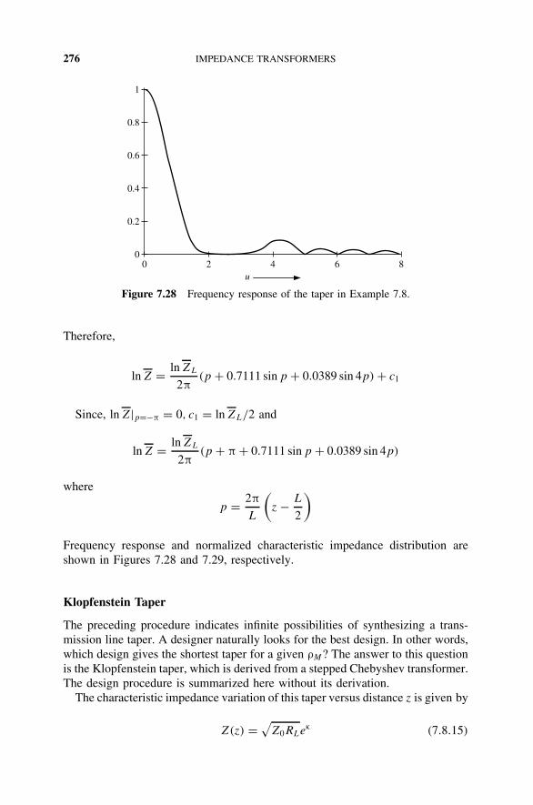
276 IMPEDANCE TRANSFORMERS
1
0.8
0.6
0.4
0.2
00 2 4 6 8
u
Figure 7.28 Frequency response of the taper in Example 7.8.
Therefore,
ln Z = ln ZL
2π(p + 0.7111 sin p + 0.0389 sin 4p) + c1
Since, ln Z|p=−π = 0, c1 = ln ZL/2 and
ln Z = ln ZL
2π(p + π + 0.7111 sin p + 0.0389 sin 4p)
where
p = 2π
L
(z − L
2
)
Frequency response and normalized characteristic impedance distribution areshown in Figures 7.28 and 7.29, respectively.
Klopfenstein Taper
The preceding procedure indicates infinite possibilities of synthesizing a trans-mission line taper. A designer naturally looks for the best design. In other words,which design gives the shortest taper for a given ρM? The answer to this questionis the Klopfenstein taper, which is derived from a stepped Chebyshev transformer.The design procedure is summarized here without its derivation.
The characteristic impedance variation of this taper versus distance z is given by
Z(z) = √Z0RLeκ (7.8.15)

SYNTHESIS OF TRANSMISSION LINE TAPERS 277
0.0 0.2 0.4 0.6 0.8 1.0
z /L
0.8
1.0
1.2
1.4
1.6
1.8
2.0N
orm
aliz
ed im
peda
nce
Figure 7.29 Normalized characteristic impedance variation of the taper in Example 7.8.
where
κ = A20
cosh Af
(2z
L− 1, A
)0 ≤ z ≤ L (7.8.16)
f (ζ, A) =∫ ζ
0
I1(A√
1 − y2)
A√
1 − y2dy |x| ≤ 1 (7.8.17)
0 = RL − Z0
RL + Z0(7.8.18)
Since the cutoff value of βL is equal to A, we have
A = β0L (7.8.19)
For a maximum ripple ρM in its passband, it can be determined as
A = cosh−1 |0|ρM
(7.8.20)
I1(x) is the modified Bessel function of the first kind. f (ζ, A) needs to be eval-uated numerically except for the following special cases:
f (0, A) = 0
f (x, 0) = x
2
f (1, A) = cosh A − 1
A2

278 IMPEDANCE TRANSFORMERS
The resulting input reflection coefficient as a function of βL (and hence, fre-quency) is given by
in(βL) = 0e−jβL cosh
√A2 − (βL)2
cosh A(7.8.21)
Note that the hyperbolic cosine becomes the cosine function for an imagi-nary argument.
Example 7.9 Design a Klopfenstein taper to match a 100- load to a 50-transmission line. The maximum allowed reflection coefficient in its passband is0.1. Plot the characteristic impedance variation along its normalized length andthe input reflection coefficient versus βL.
SOLUTION From (7.8.18),
0 = RL − Z0
RL + Z0= 100 − 50
100 + 50= 1
3
TABLE 7.1 Characteristic Impedance of theKlopfenstein Taper (in Example 7.9) as a Function ofIts Normalized Length
Z/L Impedance ()
0 56.0008960.05 57.0300430.1 58.1692550.15 59.4123370.2 60.7577240.25 62.2025180.3 63.742380.35 65.3714330.4 67.0821940.45 68.8655330.5 70.7106780.55 72.6052610.6 74.5354280.65 76.4860090.7 78.4407490.75 80.3825970.8 82.2940630.85 84.1576040.9 85.956060.95 87.6730891 89.29361

SYNTHESIS OF TRANSMISSION LINE TAPERS 279
0.0 0.2 0.4 0.6 0.8 1.0
z /L
55.0
60.0
65.0
70.0
75.0
80.0
85.0
90.0C
hara
cter
istic
impe
danc
e (Ω
)
Figure 7.30 Characteristic impedance distribution along the normalized length of theKlopfenstein taper in Example 7.9.
0.25
0.3
0.2
0.15
0.1|Γin
(βL
)|
0.05
00 5 10 15 20
βL
Figure 7.31 Reflection coefficient versus βL of the Klopfenstein taper in Example 7.9.
From (7.8.20),
A = cosh−1 |0|ρM
= cosh−113
0.1= 1.87382
Equation (7.8.15) is used to evaluate Z(z) numerically. These results are shown inTable 7.1. These data are also displayed in Figure 7.30. The reflection coefficientof this taper is depicted in Figure 7.31.
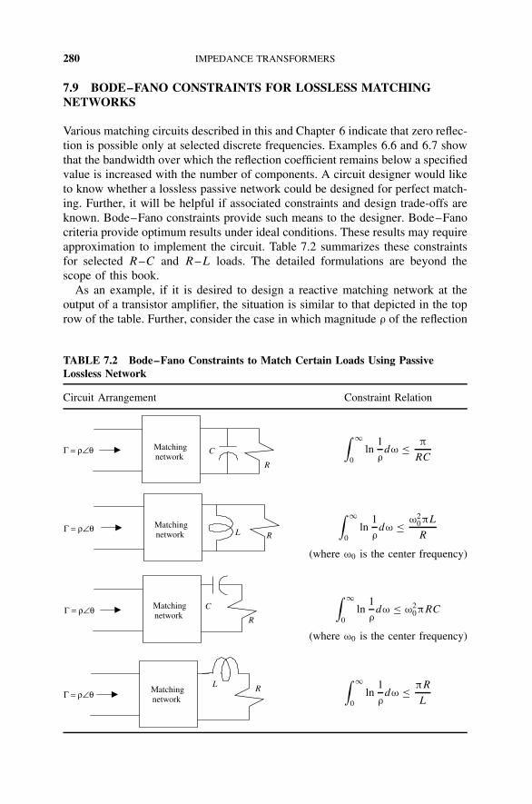
280 IMPEDANCE TRANSFORMERS
7.9 BODE–FANO CONSTRAINTS FOR LOSSLESS MATCHINGNETWORKS
Various matching circuits described in this and Chapter 6 indicate that zero reflec-tion is possible only at selected discrete frequencies. Examples 6.6 and 6.7 showthat the bandwidth over which the reflection coefficient remains below a specifiedvalue is increased with the number of components. A circuit designer would liketo know whether a lossless passive network could be designed for perfect match-ing. Further, it will be helpful if associated constraints and design trade-offs areknown. Bode–Fano constraints provide such means to the designer. Bode–Fanocriteria provide optimum results under ideal conditions. These results may requireapproximation to implement the circuit. Table 7.2 summarizes these constraintsfor selected R–C and R–L loads. The detailed formulations are beyond thescope of this book.
As an example, if it is desired to design a reactive matching network at theoutput of a transistor amplifier, the situation is similar to that depicted in the toprow of the table. Further, consider the case in which magnitude ρ of the reflection
TABLE 7.2 Bode–Fano Constraints to Match Certain Loads Using PassiveLossless Network
Circuit Arrangement Constraint Relation
R
C
Matchingnetwork
Γ = ρ∠θ
∫ ∞
0ln
1
ρdω ≤ π
RC
RL
Matchingnetwork
Γ = ρ∠θ
∫ ∞
0ln
1
ρdω ≤ ω2
0πL
R
(where ω0 is the center frequency)
R
C Γ = ρ∠θ Matchingnetwork
∫ ∞
0ln
1
ρdω ≤ ω2
0πRC
(where ω0 is the center frequency)
RL Γ = ρ∠θ Matching
network
∫ ∞
0ln
1
ρdω ≤ πR
L
PROBLEMS 281
coefficient remains constant at ρm (ρm < 1) over the frequency band from ω1 toω2, whereas it stays at unity outside this band. The constraint for this circuit isfound to be∫ ∞
0ln
1
ρdω = ln
1
ρm
∫ ω2
ω1
dω = (ω2 − ω1) ln1
ρm
≤ π
RC(7.9.1)
This condition shows the trade-off associated with the bandwidth and the reflec-tion coefficient. If R and C are given, the right-hand side of (7.9.1) is fixed. Inthis situation, a wider bandwidth (ω2 − ω1) is possible only at the cost of ahigher reflection coefficient ρm. Further, ρm cannot go to zero unless the band-width ω2 − ω1 is zero. In other words, a perfect matching condition is achievableonly at discrete frequencies.
SUGGESTED READING
Bahl, I., and P. Bhartia, Microwave Solid State Circuit Design. New York: Wiley, 1988.
Collin, R. E., Foundations for Microwave Engineering. New York: McGraw-Hill, 1992.
Elliott, R. S., An Introduction to Guided Waves and Microwave Circuits. Englewood Cliffs,NJ: Prentice Hall, 1993.
Fusco, V. F., Microwave Circuits. Englewood Cliffs, NJ: Prentice Hall, 1987.
Matthaei, G. L., L. Young, and E. M. T. Jones, Microwave Filters, Impedance-MatchingNetworks, and Coupling Structures. Dedham, MA: Artech House, 1980.
Pozar, D. M., Microwave Engineering. New York: Wiley, 1998.
PROBLEMS
7.1. The output impedance of a microwave receiver is 50 . Find the requiredlength and characteristic impedance of a transmission line that will match a100- load to the receiver. Signal frequency and phase velocity are 10 GHzand 2.4 × 10⁸ m/s, respectively. What is the frequency band over whichthe reflection coefficient remains below 0.1?
7.2. A quarter-wave impedance-matching transformer is used to match a micro-wave source with internal impedance 10 to a 50- transmission line. Ifthe source frequency is 3 GHz and the phase velocity on the line is equal tothe speed of light in free space, find (a) the required length and character-istic impedance of the matching section and (b) the reflection coefficientsat two ends of the matching section.
7.3. A 0.7-m-long transmission line short-circuited at one end has an inputimpedance of −j68.8 . The signal frequency and phase velocity are100 MHz and 2 × 10⁸ m/s, respectively.

282 IMPEDANCE TRANSFORMERS
(a) What is the characteristic impedance of the transmission line?(b) If a 200- load is connected to the end of this line, what is the new
input impedance?(c) A quarter-wave matching transformer is to be used to match a 200-
load with the line. What will be the required length and characteristicimpedance of the matching transformer?
7.4. Design a two-section binomial transformer to match a 100- load to a 75- line. What is the frequency band over which the reflection coefficientremains below 0.1?
7.5. Design a three-section binomial transformer to match a 75- load to a50- transmission line. What is the fractional bandwidth for a VSWR lessthan 1.1?
7.6. Using the approximate theory, design a two-section Chebyshev transformerto match a 100- load to a 75- line. What is the frequency band overwhich the reflection coefficient remains below 0.1? Compare the resultswith those obtained in Problem 7.4.
7.7. Design a four-section Chebyshev transformer to match a network withinput impedance 60 to a transmission line of characteristic impedance40 . Find the bandwidth if the maximum VSWR allowed in its passbandis 1.2.
7.8. Using the exact theory, design a two-section Chebyshev transformer tomatch a 10- load to a 75- line. Find the bandwidth over which thereflection coefficient remains below 0.05.
7.9. Using the exact theory, design a three-section Chebyshev transformer tomatch a 10- load to a 75- line. Find the bandwidth over which thereflection coefficient remains below 0.05. Compare the results with thoseobtained in Problem 7.8.
7.10. Design a transmission line taper to match a 75- load to a 50- line.The desired frequency response has a double zero at βL = ±2π. Plot itsfrequency response and normalized characteristic impedance distribution.
7.11. Design a transmission line taper to match a 40- load to a 75- line.Its reflection coefficient has triple zeros at βL = ±2π. Plot its frequencyresponse and normalized characteristic impedance distribution versus thenormalized length of the taper.
7.12. Design a Klopfenstein taper to match a 40- load to a 75- line. Themaximum allowed reflection coefficient in its passband is 0.1. Plot thecharacteristic impedance variation along its normalized length and the inputreflection coefficient versus βL. Compare the results with those obtainedin Problem 7.11.

8TWO-PORT NETWORKS
Electronic circuits are frequently needed for processing a given electrical signalto extract the desired information or characteristics. This includes boosting thestrength of a weak signal or filtering out certain frequency bands, and so on. Mostof these circuits can be modeled as a black box that contains a linear networkcomprising resistors, inductors, capacitors, and dependent sources. Thus, it mayinclude electronic devices but not the independent sources. Further, it has fourterminals, two for input and the other two for output of the signal. There may bea few more terminals to supply the bias voltage for electronic devices. However,these bias conditions are embedded in equivalent dependent sources. Hence, alarge class of electronic circuits can be modeled as two-port networks. Parametersof the two-port completely describe its behavior in terms of voltage and currentat each port. These parameters simplify the description of its operation when thetwo-port network is connected into a larger system.
Figure 8.1 shows a two-port network along with appropriate voltages and cur-rents at its terminals. Sometimes, port 1 is called the input port and port 2, the out-put port. The upper terminal is customarily assumed to be positive with respect tothe lower one on either side. Further, currents enter the positive terminals at eachport. Since the linear network does not contain independent sources, the same cur-rents leave respective negative terminals. There are several ways to characterizethis network. Some of these parameters and relations among them are presentedin this chapter, including impedance parameters, admittance parameters, hybrid
Radio-Frequency and Microwave Communication Circuits: Analysis and Design, Second Edition,By Devendra K. MisraISBN 0-471-47873-3 Copyright 2004 John Wiley & Sons, Inc.
283

284 TWO-PORT NETWORKS
I1 I2 +
V1
−
+
V2
−
Linear network Port 1 Port 2
Figure 8.1 Two-port network.
parameters, and transmission parameters. Scattering parameters are introducedlater in the chapter to characterize the high-frequency and microwave circuits.
8.1 IMPEDANCE PARAMETERS
Consider the two-port network shown in Figure 8.1. Since the network is linear,the superposition principle can be applied. Assuming that it contains no inde-pendent sources, voltage V1 at port 1 can be expressed in terms of two currentsas follows:
V1 = Z11I1 + Z12I2 (8.1.1)
Since V1 is in volts and I1 and I2 are in amperes, parameters Z11 and Z12 mustbe in ohms. Therefore, these are called the impedance parameters. Similarly, wecan write V2 in terms of I1 and I2 as follows:
V2 = Z21I1 + Z22I2 (8.1.2)
Using the matrix representation, we can write[V1
V2
]=
[Z11 Z12
Z21 Z22
] [I1
I2
](8.1.3)
or[V ] = [Z][I ] (8.1.4)
where [Z] is called the impedance matrix of the two-port network.If port 2 of this network is left open, I2 will be zero. In this condi-
tion, (8.1.1) and (8.1.2) give
Z11 = V1
I1
∣∣∣∣I2=0
(8.1.5)
and
Z21 = V2
I1
∣∣∣∣I2=0
(8.1.6)
Similarly, with a source connected at port 2 while port 1 is open circuit, wefind that
Z12 = V1
I2
∣∣∣∣I1=0
(8.1.7)

IMPEDANCE PARAMETERS 285
and
Z22 = V2
I2
∣∣∣∣I1=0
(8.1.8)
Equations (8.1.5) through (8.1.8) define the impedance parameters of a two-port network.
Example 8.1 Find the impedance parameters for the two-port network shownin Figure 8.2.
SOLUTION If I2 is zero, V1 and V2 can be found from Ohm’s law as 6I1.Hence, from (8.1.5) and (8.1.6),
Z11 = V1
I1
∣∣∣∣I2=0
= 6I1
I1= 6
and
Z21 = V2
I1
∣∣∣∣I2=0
= 6I1
I1= 6
Similarly, when a source is connected at port 2 and port 1 has an open circuit,we find that
V2 = V1 = 6I2
Hence, from (8.1.7) and (8.1.8),
Z12 = V1
I2
∣∣∣∣I1=0
= 6I2
I2= 6
and
Z22 = V2
I2
∣∣∣∣I1=0
= 6I2
I2= 6
Therefore, [Z11 Z12
Z21 Z22
]=
[6 66 6
]
I1 I2
+
V1
−
+
V26 Ω
−
Figure 8.2 Two-port network for Example 8.1.
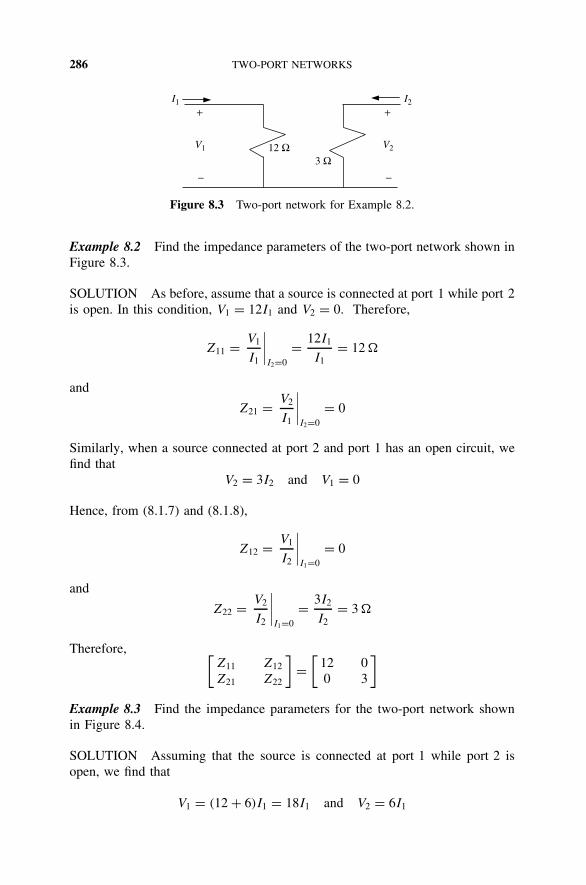
286 TWO-PORT NETWORKS
I1 I2+
V1
−
+
V2
−
12 Ω3 Ω
Figure 8.3 Two-port network for Example 8.2.
Example 8.2 Find the impedance parameters of the two-port network shown inFigure 8.3.
SOLUTION As before, assume that a source is connected at port 1 while port 2is open. In this condition, V1 = 12I1 and V2 = 0. Therefore,
Z11 = V1
I1
∣∣∣∣I2=0
= 12I1
I1= 12
and
Z21 = V2
I1
∣∣∣∣I2=0
= 0
Similarly, when a source connected at port 2 and port 1 has an open circuit, wefind that
V2 = 3I2 and V1 = 0
Hence, from (8.1.7) and (8.1.8),
Z12 = V1
I2
∣∣∣∣I1=0
= 0
and
Z22 = V2
I2
∣∣∣∣I1=0
= 3I2
I2= 3
Therefore, [Z11 Z12
Z21 Z22
]=
[12 00 3
]
Example 8.3 Find the impedance parameters for the two-port network shownin Figure 8.4.
SOLUTION Assuming that the source is connected at port 1 while port 2 isopen, we find that
V1 = (12 + 6)I1 = 18I1 and V2 = 6I1

IMPEDANCE PARAMETERS 287
I1 I2+
V1
−
+
V2
−
6 Ω
12 Ω 3 Ω
Figure 8.4 Two-port network for Example 8.3.
Note that there is no current flowing through a 3- resistor because port 2is open.
Therefore,
Z11 = V1
I1
∣∣∣∣I2=0
= 18I1
I1= 18
and
Z21 = V2
I1
∣∣∣∣I2=0
= 6I1
I1= 6
Similarly, with a source at port 2 and port 1 open circuit,
V2 = (6 + 3)I2 = 9I2 and V1 = 6I2
This time, there is no current flowing through a 12- resistor because port 1 isopen. Hence, from (8.1.7) and (8.1.8),
Z12 = V1
I2
∣∣∣∣I1=0
= 6I2
I2= 6
and
Z22 = V2
I2
∣∣∣∣I1=0
= 9I2
I2= 9
Therefore, [Z11 Z12
Z21 Z22
]=
[18 66 9
]
An analysis of results obtained in Examples 8.1 to 8.3 indicates that Z12
and Z21 are equal for all three circuits. In fact, it is an inherent characteris-tic of these networks. It will hold for any reciprocal circuit. If a given circuitis symmetrical, Z11 will be equal to Z22 as well. Further, impedance parame-ters obtained in Example 8.3 are equal to the sum of the corresponding resultsfound in Examples 8.1 and 8.2. This happens because if the circuits of these twoexamples are connected in series, we end up with the circuit of Example 8.3,shown in Figure 8.5.

288 TWO-PORT NETWORKS
I1
I1 I2
I2
+
V1
−
+
V2
−
+
V ′1
−
+
V ′2
−
12 Ω
6 Ω
3 Ω
Figure 8.5 Circuit for Example 8.3.
Example 8.4 Find the impedance parameters for a transmission line networkshown in Figure 8.6.
SOLUTION This circuit is symmetrical because interchanging port 1 and port 2does not affect it. Therefore, Z22 must be equal to Z11. Further, if current I atport 1 produces an open-circuit voltage V at port 2, current I injected at port 2will produce V at port 1. Hence, it is a reciprocal circuit. Therefore, Z12 will beequal to Z21. Assume that the source is connected at port 1 while the other portis open. If Vin is incident voltage at port 1, Vine
−γl is the voltage at port 2. Sincethe reflection coefficient of an open circuit is +1, the reflected voltage at this portis equal to the incident voltage. Therefore, the reflected voltage reaching port 1is Vine
−2γl . Hence,
V1 = Vin + Vine−2γl
V2 = 2Vine−γl
I1 = Vin
Z0(1 − e2γl)
l
I1 I2+
V1
−
+
V2Z0, γ
−
Figure 8.6 Transmission line network for Example 8.4.

ADMITTANCE PARAMETERS 289
and
I2 = 0
Therefore,
Z11 = V1
I1
∣∣∣∣I2=0
= Vin(1 + e−2γl)
(Vin/Z0)(1 − e−2γl)= Z0
e+γl + e−γl
e+γl − e−γl= Z0
tanh γl= Z0 coth γl
and
Z21 = V2
I1
∣∣∣∣I2=0
= 2Vine−γl
(Vin/Z0)(1 − e−2γl)= Z0
2
e+γl − e−γl= Z0
sinh γl
For a lossless line, γ = jβ, and therefore,
Z11 = Z0
j tan βl= −jZ0 cot βl
and
Z21 = Z0
j sin βl= −j
Z0
sin βl
8.2 ADMITTANCE PARAMETERS
Consider again the two-port network shown in Figure 8.1. Since the network islinear, the superposition principle can be applied. Assuming that it contains noindependent sources, current I1 at port 1 can be expressed in terms of two vol-tages:
I1 = Y11V1 + Y12V2 (8.2.1)
Since I1 is in amperes and V1 and V2 are in volts, parameters Y11 and Y12 mustbe in siemens. Therefore, these are called the admittance parameters. Similarly,we can write I2 in terms of V1 and V2 as follows:
I2 = Y21V1 + Y22V2 (8.2.2)
Using the matrix representation, we can write[I1
I2
]=
[Y11 Y12
Y21 Y22
] [V1
V2
](8.2.3)
or
[I ] = [Y ][V ] (8.2.4)
where [Y ] is called the admittance matrix of the two-port network.

290 TWO-PORT NETWORKS
If port 2 of this network has a short circuit, V2 will be zero. In this condi-tion, (8.2.1) and (8.2.2) give
Y11 = I1
V1
∣∣∣∣V2=0
(8.2.5)
and
Y21 = I2
V1
∣∣∣∣V2=0
(8.2.6)
Similarly, with a source connected at port 2 and a short circuit at port 1,
Y12 = I1
V2
∣∣∣∣V1=0
(8.2.7)
and
Y22 = I2
V2
∣∣∣∣V1=0
(8.2.8)
Equations (8.2.5) through (8.2.8) define the admittance parameters of a two-port network.
Example 8.5 Find the admittance parameters of the circuit shown in Figure 8.7.
SOLUTION If V2 is zero, I1 is equal to 0.05 V1 and I2 is −0.05 V1. Hence,from (8.2.5) and (8.2.6),
Y11 = I1
V1
∣∣∣∣V2=0
= 0.05 V1
V1= 0.05 S
and
Y21 = I2
V1
∣∣∣∣V2=0
= −0.05 V1
V1= −0.05 S
Similarly, with a source connected at port 2 and port 1 having a short circuit,
I2 = −I1 = 0.05 V2
I1 I2
0.05 S
+ V1−
+ V2−
Figure 8.7 Circuit for Example 8.5.

ADMITTANCE PARAMETERS 291
Hence, from (8.2.7) and (8.2.8),
Y12 = I1
V2
∣∣∣∣V1=0
= −0.05 V2
V2= −0.05 S
and
Y22 = I2
V2
∣∣∣∣V1=0
= 0.05 V2
V2= 0.05 S
Therefore, [Y11 Y12
Y21 Y22
]=
[0.05 −0.05
−0.05 0.05
]
Again we find that Y11 is equal to Y22 because this circuit is symmetrical. Simi-larly, Y12 is equal to Y21 because it is reciprocal.
Example 8.6 Find the admittance parameters for the two-port network shownin Figure 8.8.
SOLUTION Assuming that a source is connected at port 1 and port 2 has ashort circuit, we find that
I1 = 0.1(0.2 + 0.025)
0.1 + 0.2 + 0.025V1 = 0.0225
0.325V1 A
and if voltage across 0.2 S is VN , then
VN = I1
0.2 + 0.025= 0.0225
0.225 × 0.325V1 = V1
3.25V
Therefore,
I2 = −0.2 VN = − 0.2
3.25V1 A
I1 I2+
V1
−
+
V2
−
0.025 S
0.1 S 0.2 S
Figure 8.8 Two-port network for Example 8.6.

292 TWO-PORT NETWORKS
Hence, from (8.2.5) and (8.2.6),
Y11 = I1
V1
∣∣∣∣V2=0
= 0.0225
0.325= 0.0692 S
and
Y21 = I2
V1
∣∣∣∣V2=0
= − 0.2
3.25= −0.0615 S
Similarly, with a source at port 2 and port 1 having a short circuit,
I2 = 0.2(0.1 + 0.025)
0.2 + 0.1 + 0.025V1 = 0.025
0.325V2 A
and if voltage across 0.1 S is VM , then
VM = I2
0.1 + 0.025= 0.025
0.125 × 0.325V2 = 2 V2
3.25V
Therefore,
I1 = −0.1 VM = − 0.2
3.25V2 A
Hence, from (8.2.7) and (8.2.8),
Y12 = I1
V2
∣∣∣∣V1=0
= − 0.2
3.25= −0.0615 S
and
Y22 = I2
V2
∣∣∣∣V1=0
= 0.025
0.325= 0.0769 S
Therefore, [Y11 Y12
Y21 Y22
]=
[0.0692 −0.0615
−0.0615 0.0769
]
As expected, Y12 = Y21 but Y11 = Y22. This is because the given circuit is recip-rocal but is not symmetrical.
Example 8.7 Find the admittance parameters of the two-port network shown inFigure 8.9.
SOLUTION Assuming that a source is connected at port 1 and port 2 has ashort circuit, we find that
I1 =[
0.05 + 0.1(0.2 + 0.025)
0.1 + 0.2 + 0.025
]V1 = 0.1192 V1 A

ADMITTANCE PARAMETERS 293
I1 I2+
V1
−
+
V2
−
0.025 S
0.1 S
0.05 S
0.2 S
Figure 8.9 Two-port network for Example 8.7.
and if current through 0.05 S is IN , then
IN = 0.05
0.05 + [0.1(0.2 + 0.025)/(0.1 + 0.2 + 0.025)]I1 = 0.05 V1 A
Current through 0.1 S is I1 − IN = 0.0692 V1. Using the current-division rule,current IM through 0.2 S is found as follows:
IM = 0.2
0.2 + 0.0250.0692 V1 = 0.0615 V1 A
Hence, I2 = −(IN + IM) = −0.1115 V1 A.Now, from (8.2.5) and (8.2.6),
Y11 = I1
V1
∣∣∣∣V2=0
= 0.1192 S
and
Y21 = I2
V1
∣∣∣∣V2=0
= −0.1115 S
Similarly, with a source at port 2 and port 1 having a short circuit, current I2 atport 2 is
I2 =[
0.05 + 0.2(0.1 + 0.025)
0.2 + 0.1 + 0.025
]V2 = 0.1269 V2 A
and current IN through 0.05 S can be found as follows:
IN = 0.05
0.05 + [0.2(0.1 + 0.025)/(0.2 + 0.1 + 0.025)]I2 = 0.05 V2 A

294 TWO-PORT NETWORKS
0.05 S
+ V1
I1 −
+
V1
−
+
V2
−
+ V2
I2−
+
V2
−
+
V1
− 0.2 S
0.025 S
0.1 S
Figure 8.10 Circuit for Example 8.7.
Current through 0.2 S is I2 − IN = 0.0769 V2. Using the current-division rule onemore time, the current IM through 0.1 S is found as follows:
IM = 0.1
0.1 + 0.0250.0769 V2 = 0.0615V2 A
Hence, I1 = −(IN + IM) = −0.1115 V2 A. Therefore, from (8.2.7) and (8.2.8),
Y12 = I1
V2
∣∣∣∣V1=0
= −0.1115 S
and
Y22 = I2
V2
∣∣∣∣V1=0
= 0.1269 S
Therefore, [Y11 Y12
Y21 Y22
]=
[0.1192 −0.1115
−0.1115 0.1269
]
As expected, Y12 = Y21 but Y11 = Y22. This is because the given circuit is recip-rocal but is not symmetrical. Further, we find that the admittance parametersobtained in Example 8.7 are equal to the sum of the corresponding impedanceparameters of Examples 8.5 and 8.6. This is because when the circuits of thesetwo examples are connected in parallel, we end up with the circuit of Example 8.7,shown in Figure 8.10.
Example 8.8 Find the admittance parameters of a transmission line of length l,shown in Figure 8.11.

ADMITTANCE PARAMETERS 295
l
I1 I2+
V1
−
+
V2Z0, γ
−
Figure 8.11 Setup for Example 8.8.
SOLUTION This circuit is symmetrical because interchanging port 1 and port 2does not affect it. Therefore, Y22 must be equal Y11. Further, if voltage V at port 1produces a short-circuit current I at port 2, voltage V at port 2 will producecurrent I at port 1. Hence, it is a reciprocal circuit. Therefore, Y12 will be equalto Y21. Assume that a source is connected at port 1 when the other port has ashort circuit. If Vin is the incident voltage at port 1, it will appear as Vine
−γl atport 2. Since the reflection coefficient of a short circuit is equal to −1, reflectedvoltage at this port is 180 out of phase with incident voltage. Therefore, thereflected voltage reaching at port 1 is −Vine
−2γl . Hence,
V1 = Vin − Vine−2γl
V2 = 0
I1 = Vin
Z0(1 + e−2γl)
and
I2 = −2Vin
Z0e−γl
Therefore,
Y11 = I1
V1
∣∣∣∣V2=0
= (Vin/Z0)(1 + e−2γl)
Vin(1 − e−2γl)= e+γl + e−γl
Z0(e+γl − e−γl)= 1
Z0 tanh γl
and
Y21 = I2
V1
∣∣∣∣V2=0
= −(2Vin/Z0)e−γl
Vin(1 − e−2γl)= − 2
Z0(e+γl − e−γl)= − 1
Z0 sinh γl
For a lossless line, γ = jβ and therefore
Y11 = 1
jZ0 tan βl
and
Y21 = − 1
jZ0 sin βl= j
1
Z0 sin βl

296 TWO-PORT NETWORKS
8.3 HYBRID PARAMETERS
Reconsider the two-port network of Figure 8.1. Since the network is linear, thesuperposition principle can be applied. Assuming that it contains no independentsources, voltage V1 at port 1 can be expressed in terms of current I1 at port 1and voltage V2 at port 2:
V1 = h11I1 + h12V2 (8.3.1)
Similarly, we can write I2 in terms of I1 and V2:
I2 = h21I1 + h22V2 (8.3.2)
Since V1 and V2 are in volts while I1 and I2 are in amperes, parameter h11 mustbe in ohms, h12 and h21 must be dimensionless, and h22 must be in siemens.Therefore, these are called the hybrid parameters.
Using the matrix representation, we can write[V1
I2
]=
[h11 h12
h21 h22
] [I1
V2
](8.3.3)
Hybrid parameters are especially important in transistor circuit analysis. Theseparameters are determined as follows. If port 2 has a short circuit, V2 will bezero. In this condition, (8.3.1) and (8.3.2) give
h11 = V1
I1
∣∣∣∣V2=0
(8.3.4)
and
h21 = I2
I1
∣∣∣∣V2=0
(8.3.5)
Similarly, with a source connected at port 2 while port 1 is open,
h12 = V1
V2
∣∣∣∣I1=0
(8.3.6)
and
h22 = I2
V2
∣∣∣∣I1=0
(8.3.7)
Thus, parameters h11 and h21 represent the input impedance and the forwardcurrent gain, respectively, when a short circuit is at port 2. Similarly, h12 and h22
represent the reverse voltage gain and the output admittance, respectively, whenport 1 has an open circuit. Because of this mix, these are called hybrid parame-ters. In transistor circuit analysis, these are generally denoted by hi, hf , hr , andh0, respectively.

HYBRID PARAMETERS 297
I1 I2+
V1
−
+
V2
−
6 Ω
12 Ω 3 Ω
Figure 8.12 Two-port network for Example 8.9..
Example 8.9 Find the hybrid parameters of the two-port network shown inFigure 8.12.
SOLUTION With a short circuit at port 2,
V1 = I1
(12 + 6 × 3
6 + 3
)= 14I1
and using the current-divider rule, we find that
I2 = − 6
6 + 3I1 = −2
3I1
Therefore, from (8.3.4) and (8.3.5),
h11 = V1
I1
∣∣∣∣V2=0
= 14
and
h21 = I2
I1
∣∣∣∣V2=0
= −2
3
Similarly, with a source connected at port 2 while port 1 has an open circuit,
V2 = (3 + 6)I2 = 9I2
and
V1 = 6I2
because there is no current flowing through a 12- resistor. Hence, from (8.3.6)and (8.3.7),
h12 = V1
V2
∣∣∣∣I1=0
= 6I2
9I2= 2
3
and
h22 = I2
V2
∣∣∣∣I1=0
= 1
9S

298 TWO-PORT NETWORKS
Thus, [h11 h12
h21 h22
]=
[14 2
3
− 23
19 S
]
8.4 TRANSMISSION PARAMETERS
Reconsider the two-port network of Figure 8.1. Since the network is linear, thesuperposition principle can be applied. Assuming that it contains no independentsources, voltage V1 and current I1 at port 1 can be expressed in terms of currentI2 and voltage V2 at port 2 as follows:
V1 = AV2 − BI2 (8.4.1)
Similarly, we can write I1 in terms of I2 and V2 as follows:
I1 = CV2 − DI2 (8.4.2)
Since V1 and V2 are in volts while I1 and I2 are in amperes, parameters A andD must be dimensionless, B must be in ohms, and C must be in siemens.
Using the matrix representation, (8.4.2) can be written as follows:
[V1
I1
]=
[A B
C D
] [V2
−I2
](8.4.3)
Transmission parameters (also known as elements of chain matrix ) are especiallyimportant for analysis of circuits connected in cascade. These parameters aredetermined as follows. If port 2 has a short circuit, V2 will be zero. Under thiscondition, (8.4.1) and (8.4.2) give
B = V1
−I2
∣∣∣∣V2=0
(8.4.4)
and
D = I1
−I2
∣∣∣∣V2=0
(8.4.5)
Similarly, with a source connected at the port 1 while port 2 is open, we find that
A = V1
V2
∣∣∣∣I2=0
(8.4.6)
and
C = I1
V2
∣∣∣∣I2=0
(8.4.7)

TRANSMISSION PARAMETERS 299
I1 I2
1 Ω
+ V1
−
+ V2
−
Figure 8.13 Network for Example 8.10.
Example 8.10 Determine the transmission parameters of the network shown inFigure 8.13.
SOLUTION With a source connected at port 1 while port 2 has a short circuit(so that V2 is zero),
I2 = −I1 and V1 = I1V
Therefore, from (8.4.4) and (8.4.5),
B = V1
−I2
∣∣∣∣V2=0
= 1
and
D = I1
−I2
∣∣∣∣V2=0
= 1
Similarly, with a source connected at port 1 while port 2 is open (so that I2
is zero),V2 = V1 and I1 = 0
Now, from (8.4.6) and (8.4.7),
A = V1
V2
∣∣∣∣I2=0
= 1
and
C = I1
V2
∣∣∣∣I2=0
= 0
Hence, the transmission matrix of this network is[A B
C D
]=
[1 10 1
]
Example 8.11 Determine the transmission parameters of the network shown inFigure 8.14.
SOLUTION With a source connected at port 1 while port 2 has a short circuit(so that V2 is zero),
I2 = −I1 and V1 = 0V
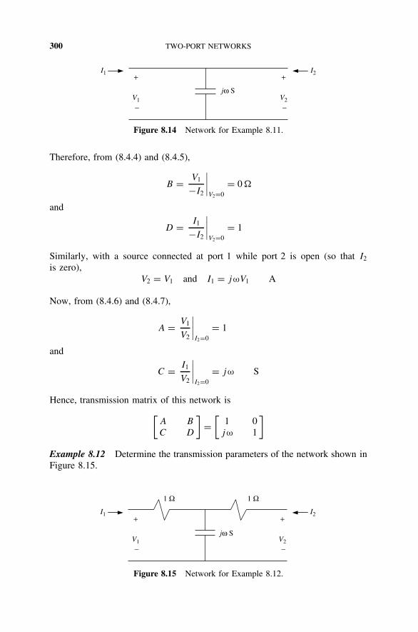
300 TWO-PORT NETWORKS
I1 I2+
V1
−
+
V2
−
jω S
Figure 8.14 Network for Example 8.11.
Therefore, from (8.4.4) and (8.4.5),
B = V1
−I2
∣∣∣∣V2=0
= 0
and
D = I1
−I2
∣∣∣∣V2=0
= 1
Similarly, with a source connected at port 1 while port 2 is open (so that I2
is zero),V2 = V1 and I1 = jωV1 A
Now, from (8.4.6) and (8.4.7),
A = V1
V2
∣∣∣∣I2=0
= 1
and
C = I1
V2
∣∣∣∣I2=0
= jω S
Hence, transmission matrix of this network is[A B
C D
]=
[1 0
jω 1
]
Example 8.12 Determine the transmission parameters of the network shown inFigure 8.15.
I1 I2+
V1
−
+
V2
−
1 Ω 1 Ω
jω S
Figure 8.15 Network for Example 8.12.

TRANSMISSION PARAMETERS 301
SOLUTION With a source connected at port 1 while port 2 has a short circuit(so that V2 is zero), we find that
V1 =(
1 + 1
1 + jω
)I1 = 2 + jω
1 + jωI1
and
I2 = −1
jω
1/jω + 1I1 = − 1
1 + jωI1
Therefore, from (8.4.4) and (8.4.5),
B = V1
−I2
∣∣∣∣V2=0
= 2 + jω
and
D = I1
−I2
∣∣∣∣V2=0
= 1 + jω
Similarly, with a source connected at port 1 while port 2 is open (so that I2
is zero),
V1 =(
1 + 1
jω
)I1 = 1 + jω
jωI1
and
V2 = 1
jωI1
Now, from (8.4.6) and (8.4.7),
A = V1
V2
∣∣∣∣I2=0
= 1 + jω
and
C = I1
V2
∣∣∣∣I2=0
= jω S
Hence, [A B
C D
]=
[1 + jω 2 + jω
jω 1 + jω
]
Example 8.13 Find the transmission parameters of the transmission line shownin Fig. 8.16.
SOLUTION Assume that a source is connected at port 1 while the other porthas a short circuit. If Vin is incident voltage at port 1, it will be Vine
−γl at port 2.

302 TWO-PORT NETWORKS
l
I1 I2+
V1
−
+
V2Z0, γ
−
Figure 8.16 Transmission line for Example 8.13.
Since the reflection coefficient of the short circuit is −1, the reflected voltage atthis port is 180 out of phase with the incident voltage. Therefore, the reflectedvoltage reaching at port 1 is −Vine
−2γl . Hence,
V1 = Vin − Vine−2γl
V2 = 0
I1 = Vin
Z0(1 + e−2γl)
and
I2 = −2Vin
Z0e−γl
Therefore, from (8.4.4) and (8.4.5),
B = V1
−I2
∣∣∣∣V2=0
= Z0
2e−γl(1 − e−2λl) = Z0
eγl − e−γl
2 = Z0 sinh γl
and
D = I1
−I2
∣∣∣∣V2=0
= 1 + e−2λl
2e−λl= eγl + e−γl
2= cosh γl
Now assume that port 2 has an open circuit while the source is still connectedat port 1. If Vin is incident voltage at port 1, Vine
−γl is at port 2. Since thereflection coefficient of an open circuit is +1, the reflected voltage at this port isequal to the incident voltage. Therefore, the reflected voltage reaching at port 1is Vine
−2γl . Hence,
V1 = Vin + Vine−2γl
V2 = 2Vine−γl
I1 = Vin
Z0(1 − e−2γl)
and
I2 = 0

TRANSMISSION PARAMETERS 303
Now, from (8.4.6) and (8.4.7),
A = V1
V2
∣∣∣∣I2=0
= 1 + e−2γl
2e−γl= cosh γl
and
C = I1
V2
∣∣∣∣I2=0
= 1 − e−2γl
2Z0e−γl
= 1
Z0sinh γl
Hence, the transmission matrix of a finite-length transmission line is
[A B
C D
]=
cosh γl Z0 sinh γl
1
Z0sinh γl cosh γl
For a lossless line, γ = jβ, and therefore it simplifies to
[A B
C D
]=
cos βl jZ0 sin βl
j1
Z0sin βl cos βl
An analysis of results obtained in Examples 8.10 to 8.13 indicates that the fol-lowing condition holds for all four circuits:
AD − BC = 1 (8.4.8)
This is because these circuits are reciprocal. In other words, if a given circuitis known to be reciprocal, (8.4.8) must be satisfied. Further, we find that trans-mission parameter A is equal to D in all four cases. This always happens whena given circuit is reciprocal.
In Example 8.11, A and D are real, B is zero, and C is imaginary. For a losslessline in Example 8.13, A and D simplify to real numbers while C and D becomepurely imaginary. This characteristic of the transmission parameters is associatedwith any lossless circuit. A comparison of the circuits in Examples 8.10 to 8.12reveals that the two-port network of Example 8.12 can be obtained by cascadingthat of Example 8.10 on the two sides of Example 8.11, as shown in Figure 8.17.
I2I1
+
V1
−
+
V2
−
8.10 8.108.11
1 Ω
jω S
1 Ω
Figure 8.17 Two-port network for Example 8.12.

304 TWO-PORT NETWORKS
Therefore, the chain (or transmission) matrix for the network shown in Example8.12 can be obtained after multiplying three chain matrices as follows:[
1 10 1
]·[
1 0jω 1
]·[
1 10 1
]=
[1 10 1
]·[
1 1jω jω + 1
]
=[
1 + jω 2 + jω
jω 1 + jω
]
This shows that chain matrices are convenient in the analysis and design ofnetworks connected in cascade.
8.5 CONVERSION OF IMPEDANCE, ADMITTANCE, CHAIN, ANDHYBRID PARAMETERS
One type of network parameter can be converted into another via the respectivedefining equations. For example, the admittance parameters of a network canbe found from its impedance parameters as follows. From (8.2.3) and (8.1.3),we find that[
I1
I2
]=
[Y11 Y12
Y21 Y22
] [V1
V2
]=
[Z11 Z12
Z21 Z22
]−1 [V1
V2
]
Hence,[Y11 Y12
Y21 Y22
]=
[Z11 Z12
Z21 Z22
]−1
= 1
Z11Z22 − Z12Z21
[Z22 −Z12
−Z21 Z11
]
Similarly, (8.3.3) can be rearranged as follows:
[I1
I2
]=
D
B−AD − BC
B
− 1
B
A
B
[
V1
V2
]
Hence, [Y11 Y12
Y21 Y22
]=
D
B−AD − BC
B
− 1
B
A
B
Relations between other parameters can be found following a similar procedure.These relations are given in Table 8.1.
8.6 SCATTERING PARAMETERS
As illustrated in preceding sections, Z-parameters are useful in analyzing seriescircuits while Y -parameters simplify the analysis of parallel (shunt) connected cir-cuits. Similarly, transmission parameters are useful for chain or cascade circuits.

SCATTERING PARAMETERS 305
TABLE 8.1 Conversions Among the Impedance, Admittance, Chain, and HybridParameters
Z11 = Y22
Y11Y22 − Y12Y21
Z12 = −Y12
Y11Y22 − Y12Y21
Z21 = −Y21
Y11Y22 − Y12Y21
Z22 = Y11
Y11Y22 − Y12Y21
Z11 = A
C
Z12 = AD − BC
C
Z21 = 1
C
Z22 = D
C
Z11 = h11h22 − h12h21
h22
Z12 = h12
h22
Z21 = −h21
h22
Z22 = 1
h22
Y11 = Z22
Z11Z22 − Z12Z21
Y12 = −Z12
Z11Z22 − Z12Z21
Y21 = −Z21
Z11Z22 − Z12Z21
Y22 = Z11
Z11Z22 − Z12Z21
Y11 = D
B
Y12 = −(AD − BC)
B
Y21 = −1
B
Y22 = A
B
Y11 = 1
h11
Y12 = −h12
h11
Y21 = h21
h11
Y22 = h11h22 − h12h21
h11
A = Z11
Z21
B = Z11Z22 − Z12Z21
Z21
C = 1
Z21
D = Z22
Z21
A = −Y22
Y21
B = −1
Y21
C = −(Y11Y22 − Y12Y21)
Y21
D = −Y11
Y21
A = −(h11h22 − h12h21)
h21
B = −h11
h21
C = −h22
h21
D = −1
h21
h11 = Z11Z22 − Z12Z21
Z22
h12 = Z12
Z22
h21 = −Z21
Z22
h22 = 1
Z22
h11 = 1
Y11
h12 = −Y12
Y11
h21 = Y21
Y11
h22 = Y11Y22 − Y12Y21
Y11
h11 = B
D
h12 = AD − BC
D
h21 = −1
D
h22 = C
D

306 TWO-PORT NETWORKS
However, the characterization procedure of these parameters requires an open orshort circuit at the other port. This extreme reflection makes it very difficult (andin certain cases, impossible) to determine the parameters of a network at radioand microwave frequencies. Therefore, a new representation based on travelingwaves is defined. This is known as the scattering matrix of the network. Elementsof this matrix are known as scattering parameters.
Figure 8.18 shows a network along with incident and reflected waves at itstwo ports. We adopt a convention of representing the incident wave by ai andthe reflected wave by bi at the ith port. Hence, a1 is an incident wave, while b1
is a reflected wave at port 1. Similarly, a2 and b2 represent incident and reflectedwaves at port 2, respectively. Assume that a source is connected at port 1 thatproduces the incident wave a1. A part of this wave is reflected back at the input(due to impedance mismatch), while the remaining signal is transmitted throughthe network. It may change in magnitude as well as in phase before emerging atport 2. Depending on the termination at this port, part of the signal is reflectedback as input to port 2. Hence, reflected wave b1 depends on incident signals a1
and a2 at the two ports. Similarly, emerging wave b2 also depends on a1 and a2.Mathematically,
b1 = S11a1 + S12a2 (8.6.1)
b2 = S21a1 + S22a2 (8.6.2)
Using the matrix notation, we can write[b1
b2
]=
[S11 S12
S21 S22
] [a1
a2
](8.6.3)
or
[b] = [S][a] (8.6.4)
where [S] is called the scattering matrix of the two-port network; Sij are knownas the scattering parameters of this network, and ai represents the incident waveat the ith port and bi represents the reflected wave at the ith port.
If port 2 is matched terminated while a1 is incident at port 1, a2 is zero. Inthis condition, (8.6.1) and (8.6.2) give
S11 = b1
a1
∣∣∣∣a2=0
(8.6.5)
Two-port network a1
b1
b2
a2
Port 1Port 2
Figure 8.18 Two-port network with associated incident and reflected waves.

SCATTERING PARAMETERS 307
and
S21 = b2
a1
∣∣∣∣a2=0
(8.6.6)
Similarly, with a source connected at port 2 while port 1 is terminated by amatched load, we find that
S12 = b1
a2
∣∣∣∣a1=0
(8.6.7)
and
S22 = b2
a2
∣∣∣∣a1=0
(8.6.8)
Hence, Sii is the reflection coefficient i at the ith port when the other port ismatched terminated. Sij is the forward transmission coefficient of the j th port ifi is greater than j , whereas it represents the reverse transmission coefficient if i
is less than j with the other port terminated by a matched load.We have not yet defined ai and bi in terms of voltage, current, or power. To
that end, we write steady-state total voltage and current at the ith port as follows:
Vi = V ini + V ref
i (8.6.9)
and
Ii = 1
Z0i
(V ini − V ref
i ) (8.6.10)
where superscripts “in” and “ref” represent the incident and reflected voltages,respectively. Z0i is the characteristic impedance at the ith port. Equations (8.6.9)and (8.6.10) can be solved to find incident and reflected voltages in terms of totalvoltage and current at the ith port. Hence,
V ini = 1
2 (Vi + Z0iIi) (8.6.11)
and
V refi = 1
2 (Vi − Z0iIi) (8.6.12)
Assuming both of the ports to be lossless so that Z0i is a real quantity, the averagepower incident at the ith port is
P ini = 1
2Re
[V in
i (I ini )∗
] = 1
2Re
[V in
i
(V in
i
Z0i
)∗]= 1
2Z0i
|V ini |2 (8.6.13)
and average power reflected from the ith port is
P refi = 1
2Re
[V ref
i (I refi )∗
] = 1
2Re
[V ref
i
(V ref
i
Z0i
)∗]= 1
2Z0i
|V refi |2 (8.6.14)

308 TWO-PORT NETWORKS
The ai and bi are defined in such a way that the squares of their magnitudesrepresent the power flowing in respective directions. Hence,
ai = V ini√
2Z0i
= 1
2
(Vi + Z0iI i√
2Z0i
)= 1
2√
2
(Vi√Z0i
+ √Z0iIi
)(8.6.15)
and
bi = V refi√
2Z0i
= 1
2
(Vi − Z0iI i√
2Z0i
)= 1
2√
2
(Vi√Z0i
− √Z0iIi
)(8.6.16)
Therefore, units of ai and bi are
√watt = volt√
ohm= ampere · √ohm
Power available from the source, Pavs, at port 1 is
Pavs = |a1|2
power reflected from port 1, Pref, is
Pref = |b1|2
and power delivered to the port (and hence to the network), Pd , is
Pd = Pavs − Pref = |a1|2 − |b1|2
Consider the circuit arrangement shown in Figure 8.19. There is a voltagesource VS1 connected at port 1 while port 2 is terminated by load impedanceZL. The source impedance is ZS . Various voltages, currents, and waves are asdepicted at the two ports of this network. Further, it is assumed that the char-acteristic impedances at port 1 and port 2 are Z01 and Z02, respectively. Inputimpedance Z1 at port 1 of the network is defined as the impedance across its ter-minals when port 2 is terminated by load ZL while source VS1 along with ZS aredisconnected. Similarly, output impedance Z2 at port 2 of the network is definedas the impedance across its terminals with load ZL disconnected and voltagesource VS1 replaced by a short circuit. Hence, source impedance ZS terminates
Two-port network
a1
b1
b2
a2 Port 1
Port 2VS1
ZS
ZL
I1 I2
V1
+
−
V2
+
−
Figure 8.19 Two-port network with a voltage source connected at port 1 and port 2 isterminated.

SCATTERING PARAMETERS 309
port 1 of the network in this case. Input impedance Z1 and output impedance Z2
are responsible for input reflection coefficient 1 and output reflection coefficient2, respectively. Hence, the ratio of b1 to a1 represents 1 while that of b2 to a2
is 2. For the two-port network, we can write
b1 = S11a1 + S12a2 (8.6.17)
and
b2 = S21a1 + S22a2 (8.6.18)
The load reflection coefficient L is
L = ZL − Z02
ZL + Z02= a2
b2(8.6.19)
Note that b2 leaves port 2, and therefore it is incident on the load ZL. Similarly,the wave reflected back from the load enters port 2 as a2. The source reflectioncoefficient S is found as
S = ZS − Z01
ZS + Z01= a1
b1(8.6.20)
Since b1 leaves port 1 of the network, it is the incident wave on ZS , while a1 isthe reflected wave.
The input and output reflection coefficients are
1 = Z1 − Z01
Z1 + Z01= b1
a1(8.6.21)
and
2 = Z2 − Z02
Z2 + Z02= b2
a2(8.6.22)
Dividing (8.6.17) by a1 and then using (8.6.21), we find that
b1
a1= 1 = Z1 − Z01
Z1 + Z01= S11 + S12
a2
a1(8.6.23)
Now, dividing (8.6.18) by a2 and then combining with (8.6.19), we get
b2
a2= S22 + S21
a1
a2= 1
L
⇒ a1
a2= 1 − S22L
S21L
(8.6.24)
From (8.6.23) and (8.6.24),
1 = S11 + S12S21L
1 − S22L
(8.6.25)

310 TWO-PORT NETWORKS
If a matched load is terminating port 2, then L = 0 and (7.6.25) simplifies to1 = S11.
Similarly, from (8.6.18) and (8.6.22),
b2
a2= 2 = Z2 − Z02
Z2 + Z02= S22 + S21
a1
a2(8.6.26)
From (8.6.17) and (8.6.20), we have
b1
a1= S11 + S12
a2
a1= 1
S
⇒ a2
a1= 1 − S11S
S12S
(8.6.27)
Substituting (8.6.27) into (8.6.26), we get
2 = S22 + S21S12S
1 − S11S
(8.6.28)
If ZS is equal to Z01, port 1 is matched and S = 0. Therefore, (8.6.28) simpli-fies to
2 = S22
Hence, S11 and S22 can be found by evaluating the reflection coefficients atrespective ports while the other port is matched terminated.
Let us determine the other two parameters, S21 and S12, of the two-port net-work. Starting with (8.6.6) for S21, we have
S21 = b2
a1
∣∣∣∣a2=0
(8.6.6)
Now, a2 is found from (8.6.15) with i as 2 and forcing it to zero, we get
a2 = 1
2
(V2 + Z02I2√
2Z02
)= 0 ⇒ V2 = −Z02I2 (8.6.29)
Substituting (8.6.29) in the expression for b2 that is obtained from (8.6.16) withi as 2, we find that
b2 = 1
2
(V2 − Z02I2√
2Z02
)= −I2
√Z02
2(8.6.30)
An expression for a1 is obtained from (8.6.15) with i = 1. It simplifies for ZS
equal to Z01 as follows:
a1 = 1
2
(V1 + Z01I1√
2Z01
)= VS1
2√
2Z01(8.6.31)

SCATTERING PARAMETERS 311
S21 is obtained by substituting (8.6.30) and (8.6.31) into (8.6.6) as follows:
S21 = b2
a1
∣∣∣∣a2=0
= −√Z02I2/
√2
VS1/2√
2Z01= 2V2
VS1
√Z01
Z02(8.6.32)
Following a similar procedure, S12 may be found as
S12 = b1
a2
∣∣∣∣a1=0
= 2V1
VS2
√Z02
Z01(8.6.33)
An analysis of S-parameters indicates that
|S11|2 = |b1|2|a1|2
∣∣∣∣a2=0
= Pavs − Pd
Pavs(8.6.34)
where Pavs is power available from the source and Pd is power delivered toport 1. These two powers will be equal if the source impedance is conjugate ofZ1; that is, the source is matched with port 1. Similarly, from (8.6.32),
|S21|2 = Z02(I2/√
2)2
( 14Z01)(VS1/
√2)2
= Z02(I2/√
2)2
12 [(1/2Z01)(VS1/
√2)2]
= PAVN
Pavs(8.6.35)
where PAVN is power available at port 2 of the network. It will be equal to powerdelivered to a load that is matched to the port. This power ratio of (8.6.35) maybe called the transducer power gain.
Following a similar procedure, it may be found that |S22|2 represents the ratioof power reflected from port 2 to power available from the source at port 2,while port 1 is terminated by a matched load ZS and |S12|2 represents a reversetransducer power gain.
Shifting the Reference Planes
Consider the two-port network shown in Figure 8.20. Assume that ai and bi areincident and reflected waves, respectively, at unprimed reference planes of the ith
Two-port network a1
b1
b2
a2 Port 1
Port 2
AA′
A′ A B
B
B′
B′
x1 x2
l1 l2
Figure 8.20 Two-port network with two reference planes on each side.

312 TWO-PORT NETWORKS
port. We use unprimed S-parameters for this case. Next, consider that plane A–Ais shifted by a distance l1 to A′ –A′. At this plane, a′
1 and b′1 represent inward- and
outward-traveling waves, respectively. Similarly, a′2 and b′
2 represent inward- andoutward-traveling waves, respectively, at plane B′ –B′. We denote the scatteringparameters at primed planes by a prime on each as well. Hence,[
b1
b2
]=
[S11 S12
S21 S22
] [a1
a2
](8.6.36)
and [b′
1b′
2
]=
[S ′
11 S ′12
S ′21 S ′
22
] [a′
1a′
2
](8.6.37)
Wave b1 is delayed in phase by βl1 as it travels from A to A′. This means thatb1 is ahead in phase with respect to b′
1. Hence,
b1 = b′1e
jβl1 (8.6.38)
Wave a1 comes from A′ to plane A. Therefore, it has a phase delay of βl1 withrespect to a′
1. Mathematically,
a1 = a′1e
−jβl1 (8.6.39)
On the basis of similar considerations at port 2, we can write
b2 = b′2e
jβl2 (8.6.40)
and
a2 = a′2e
−jβl2 (8.6.41)
Substituting for b1, a1, b2, and a1 from (8.6.38) to (8.6.41) into (8.6.36), we get
[b′
1ejβl1
b′2e
jβl2
]=
[S11 S12
S21 S22
][a′
1e−jβl1
a′2e
−jβl2
](8.6.42)
We can rearrange this equation as follows:
[b′
1
b′2
]=
[S11e
−j2βl1 S12e−jβ(l1+l2)
S21e−jβ(l1+l2) S22e
−j2βl2
][a′
1
a′2
](8.6.43)
Now, on comparing (8.6.43) with (8.6.37), we find that
[S ′
11 S ′12
S ′21 S ′
22
]=
[S11e
−j2βl1 S12e−jβ(l1+l2)
S21e−jβ(l1+l2) S22e
−j2βl2
](8.6.44)

SCATTERING PARAMETERS 313
Two-port network
V2V1
I1 I2
Figure 8.21 Network for Example 8.14.
Following a similar procedure, one can find the other relation as follows:
[S11 S12
S21 S22
]=
[S ′
11ej2βl1 S ′
12ejβ(l1+l2)
S ′21e
jβ(l1+l2) S ′22e
j2βl2
](8.6.45)
Example 8.14 The total voltages and currents at two ports of a network arefound as follows: V1 = 10 0V, I1 = 0.1 40A, V2 = 12 30V, and I2 =0.15 100A. Determine the incident and reflected voltages, assuming that thecharacteristic impedance is 50 at both its ports (see Figure 8.21).
SOLUTION From (8.6.11) and (8.6.12) with i = 1, we find that
V in1 = 1
2 (10 0 + 50 × 0.1 40) = 6.915 + j1.607 V
and
V ref1 = 1
2 (10 0 − 50 × 0.1 40) = 3.085 − j1.607 V
Similarly, with i = 2, incident and reflected voltages at port 2 are found to be
V in2 = 1
2 (12 30 + 50 × 0.15 100) = 4.545 + j6.695 V
and
V ref2 = 1
2 (12 30 − 50 × 0.15 100) = 5.845 − j0.691 V
Example 8.15 Find the S-parameters of a series impedance Z connected bet-ween the two ports, as shown in Figure 8.22.
Z
Z0 Z0
Figure 8.22 Setup for Example 8.15.

314 TWO-PORT NETWORKS
SOLUTION From (8.6.25), with L = 0 (i.e., port 2 is terminated by a matchedload), we find that
S11 = 1|a2=0 = (Z + Z0) − Z0
(Z + Z0) + Z0= Z
Z + 2Z0
Similarly, from (8.6.28), with S = 0 (i.e., port 1 is terminated by a matchedload),
S22 = 2|a1=0 = (Z + Z0) − Z0
(Z + Z0) + Z0= Z
Z + 2Z0
S21 and S12 are determined from (8.6.32) and (8.6.33), respectively. For evaluat-ing S21, we connect a voltage source VS1 at port 1 while port 2 is terminated byZ0, as shown in Figure 8.23. The source impedance is Z0.
Using the voltage-divider formula, we can write
V2 = Z0
Z + 2Z0VS1
Hence, from (8.6.32),
S21 = 2V2
VS1= 2Z0
Z + 2Z0= 2Z0 + Z − Z
Z + 2Z0= 1 − Z
Z + 2Z0
For evaluating S12, we connect a voltage source VS2 at port 2 while port 1 isterminated by Z0, as shown in Figure 8.24. The source impedance is Z0. Usingthe voltage-divider rule again, we find that
V1 = Z0
Z + 2Z0VS2
Z Z0
VS1 ~ V1 V2
Z0
Figure 8.23 Setup to determine S21 for Example 8.15.
Z0Z
VS2~V1 V2Z0
Figure 8.24 Setup to determine S12 for Example 8.15.

SCATTERING PARAMETERS 315
Now, from (8.6.33),
S12 = 2V1
VS2= 2Z0
Z + 2Z0= 2Z0 + Z − Z
Z + 2Z0= 1 − Z
Z + 2Z0
Therefore, [S11 S12
S21 S22
]=
[1 1 − 1
1 − 1 1
]
where
1 = Z
Z + 2Z0
An analysis of the S-parameters indicates that S11 is equal to S22. This is becausethe given two-port network is symmetrical. Further, its S12 is equal to S21 as well.This happens because this network is reciprocal.
Consider a special case where the series impedance Z is a purely reactiveelement, which means that Z is equal to jX. In that case, 1 can be written as
1 = jX
jX + 2Z0
Therefore,
|S11|2 + |S21|2 =∣∣∣∣ jX
jX + 2Z0
∣∣∣∣2
+∣∣∣∣1 − jX
jX + 2Z0
∣∣∣∣2
= X2
X2 + (2Z0)2+ (2Z0)
2
X2 + (2Z0)2= 1
Similarly,|S12|2 + |S22|2 = 1
On the other hand,
S11S∗12 + S21S
∗22 = jX
jX + 2Z0× 2Z0
−jX + 2Z0+ 2Z0
jX + 2Z0× −jX
−jX + 2Z0= 0
and
S12S∗11 + S22S
∗21 = 2Z0
jX + 2Z0× −jX
−jX + 2Z0+ jX
jX + 2Z0× 2Z0
−jX + 2Z0= 0
These characteristics of the scattering matrix can be summarized as follows:
∑SijS
∗ik = δjk =
1 if j = k
0 otherwise

316 TWO-PORT NETWORKS
YZ0 Z0
Figure 8.25 Network for Example 8.16.
When the elements of a matrix satisfy this condition, it is called a unitary matrix.Hence, the scattering matrix of a reactance circuit is unitary.
Example 8.16 Find the S-parameters of a shunt admittance Y connected bet-ween two ports, as shown in Figure 8.25.
SOLUTION From (8.6.25),
S11 = 1|L=0 = Z1 − Z01
Z1 + Z01= 1/Y1 − 1/Y0
1/Y1 + 1/Y0
= Y0 − Y1
Y0 + Y1= Y0 − (Y + Y0)
Y0 + (Y + Y0)= −Y
2Y0 + Y
Similarly, from (8.6.28),
S22 = 2|S=0 = Z2 − Z02
Z2 + Z02= 1/Y2 − 1/Y0
1/Y2 + 1/Y0
= Y0 − Y2
Y0 + Y2= Y0 − (Y + Y0)
Y0 + (Y + Y0)= −Y
2Y0 + Y
For evaluating S21, voltage source VS1 is connected at port 1, and port 2 is ter-minated by a matched load, as shown in Figure 8.26.
Using the voltage-divider rule,
V2 = 1/(Y + Y0)
Z0 + 1/(Y + Y0)VS1 = 1
Z0(Y + Y0) + 1VS1 = Y0
Y + 2Y0VS1
Now, from (8.6.32),
S21 = 2V2
VS1
∣∣∣∣L=0
= 2Y0
Y + 2Y0= 1 − Y
Y + 2Y0= 1 + 1
YZ0
Z0VS1 V1 V2~
Figure 8.26 Setup to determine S21 for Example 8.16.

SCATTERING PARAMETERS 317
Similarly, when VS2 in series with Z0 is connected at port 2 while port 1 ismatch-terminated, S12 can be found from (8.6.33) as follows:
S12 = 2V1
VS2
∣∣∣∣S=0
= 2Y0
Y + 2Y0= 1 − Y
Y + 2Y0= 1 + 1
where
1 = − Y
Y + 2Y0
As expected, S11 = S22 and S12 = S21, because this circuit is symmetrical as wellas reciprocal. Further, for Y = jB, the network becomes lossless. In that case,
|S11|2 + |S21|2 = B2
B2 + (2Y0)2+ (2Y0)
2
B2 + (2Y0)2= 1
and
S11S∗12 + S21S
∗22 = −jB
jB + 2Y0× 2Y0
−jB + 2Y0+ 2Y0
jB + 2Y0× jB
−jB + 2Y0= 0
Hence, with Y as jB, the scattering matrix is unitary. In fact, it can easily beproved that the scattering matrix of any lossless two-port network is unitary.
Example 8.17 An ideal transformer is designed to operate at 500 MHz. It has1000 turns on its primary side and 100 turns on its secondary side. Assuming thatit has a 50- connector on each side, determine its S-parameters (see Figure 8.27).
SOLUTION For an ideal transformer,
V1
V2= −I2
I1= n and
V1
V2
(−I2)
I1= V1/I1
V2/(−I2)= Z1
Z2= n2
Now, following the procedure used in preceding examples, we find that
S11 = b1
a1
∣∣∣∣a2=0
= 1|a2=0 = Z0n2 − Z0
Z0n2 + Z0= n2 − 1
n2 + 1= 99
101
+
V1
−
+V2
−
Port 1
Port 2
n :1
1000 :100
I1
I2
Figure 8.27 Transformer for Example 8.17.

318 TWO-PORT NETWORKS
and voltage V1 on the primary side of the transformer due to a voltage sourceVS1 with its internal impedance Z0 can be determined by the voltage-divider ruleas follows:
V1 = Z0n2
Z0n2 + Z0VS1 ⇒ V1
VS1= n2
n2 + 1= nV2
VS1
Hence,
S21 = 2V2
VS1
∣∣∣∣a2=0
= 2n
n2 + 1= 20
101
Similarly, S22 and S12 are determined after connecting a voltage source VS2 withits internal impedance Z0 at port 2. Port 1 is terminated by a matched load thistime. Therefore,
S22 = b2
a2
∣∣∣∣a1=0
= 2|a1=0 = (Z0/n2) − Z0
(Z0/n2) + Z0= 1 − n2
1 + n2= − 99
101
and
V2 = Z0/n2
(Z0/n2) + Z0VS2 ⇒ V2
VS2= 1/n2
(1/n2) + 1= 1
1 + n2= V1/n
VS2
Hence,
S12 = 2V1
VS2
∣∣∣∣a1=0
= 2n
n2 + 1= 20
101
Thus, [S11 S12
S21 S22
]=
[99
10120
10120
101 − 99101
]
This time, S11 is different from S22 because the network is not symmetrical.However, S12 is equal to S21 because it is reciprocal. Further, an ideal transformeris lossless. Hence, its scattering matrix must be unitary. Let us verify if that isthe case.
|S11|2 + |S21|2 =(
99
101
)2
+(
20
101
)2
= 10,201
10,201= 1
|S12|2 + |S22|2 =(
20
101
)2
+(
− 99
101
)2
= 10,201
10,201= 1
S11S∗12 + S21S
∗22 = 99
101× 20
101+ 20
101×
(− 99
101
)= 0
and
S12S∗11 + S22S
∗21 = 20
101× 99
101+
(− 99
101
)× 20
101= 0
Hence, the scattering matrix is indeed unitary.

SCATTERING PARAMETERS 319
l
+
V1
−
+
V2
−
I1 I2
Z0, γ
a1
a2b1
b2
Figure 8.28 Transmission line network for Example 8.18.
Example 8.18 Find the scattering parameters of the transmission line networkshown in Figure 8.28.
SOLUTION With port 2 match-terminated, wave a1 entering port 1 emergesas a1e
−γl at port 2. This wave is absorbed by the termination, making a2 zero.Further, b1 is zero as well because Z1 is equal to Z0 in this case. Hence,
b2 = a1e−γl
Similarly, when a source is connected at port 2 while port 1 is match-terminated,we find that a1 and b2 are zero and
b1 = a2e−γl
Hence, [S11 S12
S21 S22
]=
[0 e−γl
e−γl 0
]
As expected, S11 = S22 and S12 = S21, because this circuit is symmetrical as wellas reciprocal. Further, for γ = jβ, the network becomes lossless. In that case,[
S11 S12
S21 S22
]=
[0 e−jβl
e−jβl 0
]
Obviously, it is a unitary matrix now.
Example 8.19 Find the scattering parameters of the two-port network shown inFigure 8.29.
SOLUTION With port 2 matched-terminated by a 50- load, impedance Z1 atport 1 is
Z1 = j50 + 50(−j25)
50 − j25= j50 + 10 − j20 = 10 + j30

320 TWO-PORT NETWORKS
j50 Ω
−j25 ΩZ01 = 50 Ω Z02 = 50 Ω
Port 1 Port 2
Figure 8.29 Two-port network for Example 8.19.
Therefore,
S11 = 1|a2=0 = Z1 − Z01
Z1 + Z01= 10 + j30 − 50
10 + j30 + 50= 0.74536 116.565
Similarly, output impedance Z2 at port 2 when port 1 is match-terminated by a50- load is
Z2 = (50 + j50)(−j25)
50 + j50 − j25= 10 − j30
and from (8.6.32),
S22 = 2|a1=0 = Z2 − Z02
Z1 + Z02= 10 − j30 − 50
10 − j30 + 50= 0.74536 − 116.565
Now, let us connect a voltage source VS1 with its impedance at 50 at port 1while port 2 is matched, as shown in Figure 8.30. Using the voltage-divider rule,we find that
V2 = 10 − j20
50 + j50 + 10 − j20VS1
Therefore,
S21 = 2V2
VS1
∣∣∣∣a2=0
= 210 − j20
60 + j30= 0.66666 − 90
50 Ω
j50 Ω
−j25 ΩZ01 = 50 Ω Z02 = 50 Ω
Port 1
Port 2
50 Ω
VS1
V2
~
Figure 8.30 Setup to determine S21 for Example 8.19.
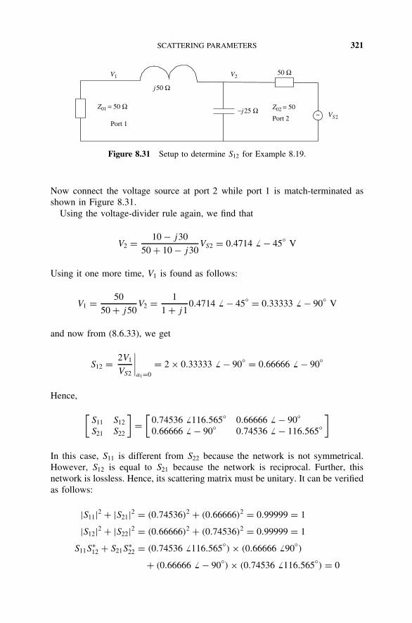
SCATTERING PARAMETERS 321
VS2
j50 Ω
−j25 ΩZ01 = 50 Ω Z02 = 50
Port 1Port 2
50 ΩV1 V2
~
Figure 8.31 Setup to determine S12 for Example 8.19.
Now connect the voltage source at port 2 while port 1 is match-terminated asshown in Figure 8.31.
Using the voltage-divider rule again, we find that
V2 = 10 − j30
50 + 10 − j30VS2 = 0.4714 − 45 V
Using it one more time, V1 is found as follows:
V1 = 50
50 + j50V2 = 1
1 + j10.4714 − 45 = 0.33333 − 90 V
and now from (8.6.33), we get
S12 = 2V1
VS2
∣∣∣∣a1=0
= 2 × 0.33333 − 90 = 0.66666 − 90
Hence,
[S11 S12
S21 S22
]=
[0.74536 116.565 0.66666 − 90
0.66666 − 90 0.74536 − 116.565]
In this case, S11 is different from S22 because the network is not symmetrical.However, S12 is equal to S21 because the network is reciprocal. Further, thisnetwork is lossless. Hence, its scattering matrix must be unitary. It can be verifiedas follows:
|S11|2 + |S21|2 = (0.74536)2 + (0.66666)2 = 0.99999 = 1
|S12|2 + |S22|2 = (0.66666)2 + (0.74536)2 = 0.99999 = 1
S11S∗12 + S21S
∗22 = (0.74536 116.565
) × (0.66666 90)
+ (0.66666 − 90) × (0.74536 116.565
) = 0

322 TWO-PORT NETWORKS
and
S12S∗11 + S22S
∗21 = (0.66666 − 90
) × (0.74536 − 116.565)
+ (0.74536 − 116.565) × (0.66666 90
)
= 0
Hence, this scattering matrix is indeed unitary.Table 8.2 summarizes the characteristics of parameter matrices of reciprocal
and symmetrical two-port networks. The properties of scattering parameters oflossless junctions are listed in Table 8.3.
TABLE 8.2 Properties of Parameters ofReciprocal and Symmetrical Two-PortNetworks
Parameter Matrix Properties[Z11 Z12
Z21 Z22
]Z12 = Z21
Z11 = Z22[Y11 Y12
Y21 Y22
]Y12 = Y21
Y11 = Y22[A B
C D
]AD − BC = 1
A = D[S11 S12
S21 S22
]S12 = S21
S11 = S22
TABLE 8.3 Properties of Scattering Matrix of Lossless Junctions
Properties Explanation
Matrix [S] is symmetrical. [S]t = [S], where [S]t is the transpose matrix of [S].Consequently,
Sij = Sji
Matrix [S] is unitary. [S]a = [S∗]t = [S]−1, where [S]a is the adjoint matrix of[S], [S∗]t is the conjugate of [S]t , and [S]−1 is theinverse matrix of [S]. Consequently,
N∑i=1
SijS∗ik = δjk =
1 for j = k
0 otherwise
Therefore,
N∑i=1
SijS∗ij =
N∑i=1
|Sij |2 = 1, j = 1, 2, 3, . . . , N

CONVERSION TO AND FROM SCATTERING PARAMETERS 323
8.7 CONVERSION FROM IMPEDANCE, ADMITTANCE, CHAIN,AND HYBRID PARAMETERS TO SCATTERING PARAMETERS,OR VICE VERSA
From (8.1.3) we can write
Vi√2Z0i
= 1√2Z0i
2∑k=1
ZikIk =2∑
k=1
Zik
Z0i
√Z0i
2Ik
=2∑
k=1
Zik
√Z0i
2Ik where i = 1, 2
Therefore, from (8.6.15) and (8.6.16), we have
ai = 1
2
2∑k=1
(Zik + δik)
√Z0i
2Ik (8.7.1)
and
bi = 1
2
2∑k=1
(Zik − δik)
√Z0i
2Ik (8.7.2)
where
δik =
1 for i = k
0 otherwise
Equations (8.7.1) and (8.7.2) can be written in matrix form as follows:
[a] = 12 [Z] + [U ][I ] (8.7.3)
[b] = 12 [Z] − [U ][I ] (8.7.4)
where
I k =√
Z0i
2Ik
and [U ] is the unit matrix.From (8.7.3) and (8.7.4), we have
[b] = [Z] − [U ][Z] + [U ]−1[a] (8.7.5)
Hence,[S] = [Z] − [U ][Z] + [U ]−1 (8.7.6)

324 TWO-PORT NETWORKS
TABLE 8.4 Conversion from (to) Impedance, Admittance, Chain, or Hybrid to(from) Scattering Parameters
S11 = (Z11 − Z∗01)(Z22 + Z02) − Z12Z21
(Z11 + Z01)(Z22 + Z02) − Z12Z21
S12 = 2Z12√
R01R02
(Z11 + Z01)(Z22 + Z02) − Z12Z21
S21 = 2Z21√
R01R02
(Z11 + Z01)(Z22 + Z02) − Z12Z21
S22 = (Z11 + Z01)(Z22 − Z∗02) − Z12Z21
(Z11 + Z01)(Z22 + Z02) − Z12Z21
Z11 = (Z∗01 + S11Z01)(1 − S22) + S12S21Z01
(1 − S11)(1 − S22) − S12S21
Z12 = 2S12√
R01R02
(1 − S11)(1 − S22) − S12S21
Z21 = 2S21√
R01R02
(1 − S11)(1 − S22) − S12S21
Z22 = (Z∗02 + S22Z02)(1 − S11) + S12S21Z02
(1 − S11)(1 − S22) − S12S21
S11 = (1 − Y11Z∗01)(1 + Y22Z02) + Y12Y21Z
∗01Z02
(1 + Y11Z01)(1 + Y22Z02) − Y12Y21Z01Z02
S12 = −2Y12√
R01R02
(1 + Y11Z01)(1 + Y22Z02) − Y12Y21Z01Z02
S21 = −2Y21√
R01R02
(1 + Y11Z01)(1 + Y22Z02) − Y12Y21Z01Z02
S22 = (1 + Y11Z01)(1 − Y22Z∗02) + Y12Y21Z01Z
∗02
(1 + Y11Z01)(1 + Y22Z02) − Y12Y21Z01Z02
Y11 = (1 − S11)(Z∗02 + S22Z02) + S12S21Z02
(Z∗01 + S11Z01)(Z
∗02 + S22Z02) − S12S21Z01Z02
Y12 = −2S12√
R01R02
(Z∗01 + S11Z01)(Z
∗02 + S22Z02) − S12S21Z01Z02
Y21 = −2S21√
R01R02
(Z∗01 + S11Z01)(Z
∗02 + S22Z02) − S12S21Z01Z02
Y22 = (Z∗01 + S11Z01)(1 − S22) + S12S21Z01
(Z∗01 + S11Z01)(Z
∗02 + S22Z02) − S12S21Z01Z02
S11 = AZ02 + B − CZ∗01Z02 − DZ∗
01
AZ02 + B + CZ01Z02 + DZ01
S12 = 2(AD − BC)(√
R01R02)
AZ02 + B + CZ01Z02 + DZ01
S21 = 2√
R01R02
AZ02 + B + CZ01Z02 + DZ01
S22 = −AZ∗02 + B − CZ01Z
∗02 + DZ01
AZ02 + B + CZ01Z02 + DZ01
A = (Z∗01 + S11Z01)(1 − S22) + S12S21Z01
2S21√
R01R02
B = (Z∗01 + S11Z01)(Z
∗02 + S22Z02) − S12S21Z01Z02
2S21√
R01R02
C = (1 − S11)(1 − S22) − S12S21
2S21√
R01R02
D = (1 − S11)(Z∗02 + S22Z02) + S12S21Z02
2S21√
R01R02
S11 = (h11 − Z∗01)(1 + h22Z02) − h12h21Z02
(Z01 + h11)(1 + h22Z02) − h12h21Z02
S12 = 2h12√
R01R02
(Z01 + h11)(1 + h22Z02) − h12h21Z02
S21 = −2h21√
R01R02
(Z01 + h11)(1 + h22Z02) − h12h21Z02
S22 = (Z01 + h11)(1 − h22Z∗02) + h12h21Z
∗02
(Z01 + h11)(1 + h22Z02) − h12h21Z02
h11 = (Z∗01 + S11Z01)(Z
∗02 + S22Z02) + S12S21Z01Z02
(1 − S11)(Z∗02 + S22Z02) + S12S21Z02
h12 = 2S12√
R01R02
(1 − S11)(Z∗02 + S22Z02) + S12S21Z02
h21 = −2S21√
R01R02
(1 − S11)(Z∗02 + S22Z02) + S12S21Z02
h22 = (1 − S11)(1 − S22) − S12S21
(1 − S11)(Z∗02 + S22Z02) + S12S21Z02
or[Z] = [U ] + [S][U ] − [S]−1 (8.7.7)
Similarly, other conversion relations can be developed. Table 8.4 lists theseequations when the two ports have different complex characteristic impedan-ces. Characteristic impedance at port 1 is assumed Z01, with its real part as R01.Similarly, characteristic impedance at port 2 is Z02, with its real part as R02.

SUGGESTED READING 325
TABLE 8.5 Conversion Between Scattering andChain Scattering Parameters
S11 = T21
T11
S12 = T11T22 − T12T21
T11
S21 = 1
T11
S22 = −T12
T11
T11 = 1
S21
T12 = −S22
S21
T21 = S11
S21
T22 = −(S11S22 − S12S21)
S21
8.8 CHAIN SCATTERING PARAMETERS
Chain scattering parameters, also known as scattering transfer parameters or T -parameters, are useful for networks in cascade. These are defined on the basis ofwaves a1 and b1 at port 1 as dependent variables and waves a2 and b2 at port 2as independent variables. Hence,
[a1
b1
]=
[T11 T12
T21 T22
] [b2
a2
]
Conversion relations of chain scattering parameters with others can easily bedeveloped. Conversions between S- and T-parameters are listed in Table 8.5.
SUGGESTED READING
Bahl, I., and P. Bhartia, Microwave Solid State Circuit Design. New York: Wiley,1988.
Collin, R. E., Foundations for Microwave Engineering. New York: McGraw-Hill,1992.
Elliott, R. S., An Introduction to Guided Waves and Microwave Circuits. Englewood Cliffs,NJ: Prentice Hall, 1993.
Fusco, V. F., Microwave Circuits. Englewood Cliffs, NJ: Prentice Hall, 1987.
Gonzalez, G., Microwave Transistor Amplifiers. Upper Saddle River, NJ: Prentice Hall,1997.
Pozar, D. M., Microwave Engineering. New York: Wiley, 1998.
Ramo, S., J. R. Whinnery, and T. Van Duzer, Fields and Waves in Communication Elec-tronics. New York: Wiley, 1994.
Rizzi, P. A., Microwave Engineering. Englewood Cliffs, NJ: Prentice Hall, 1988.
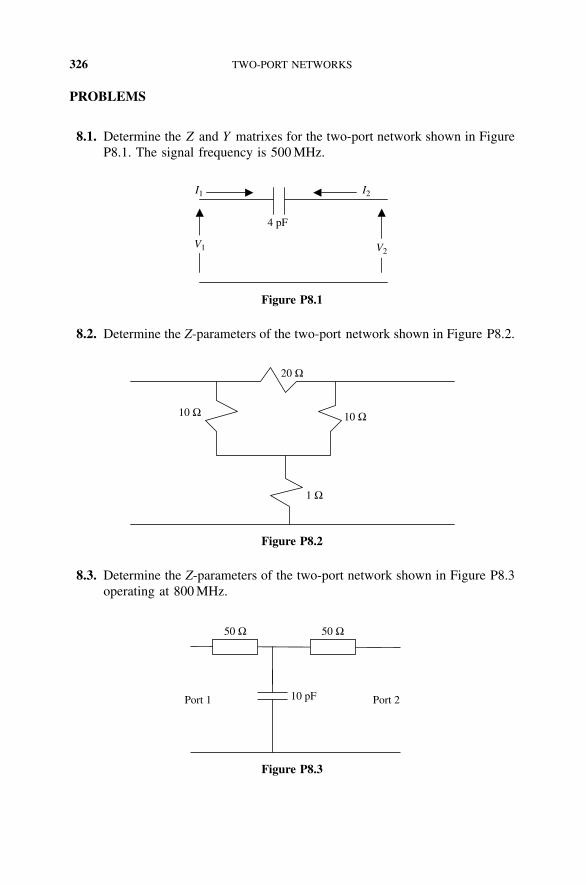
326 TWO-PORT NETWORKS
PROBLEMS
8.1. Determine the Z and Y matrixes for the two-port network shown in FigureP8.1. The signal frequency is 500 MHz.
V1 V2
I2I1
4 pF
Figure P8.1
8.2. Determine the Z-parameters of the two-port network shown in Figure P8.2.
1 Ω
10 Ω 10 Ω
20 Ω
Figure P8.2
8.3. Determine the Z-parameters of the two-port network shown in Figure P8.3operating at 800 MHz.
10 pF
50 Ω 50 Ω
Port 1 Port 2
Figure P8.3

PROBLEMS 327
8.4. Determine the Z-matrix for the two-port network shown in Figure P8.4.
j2 Ω j3 Ω
j4 Ω
Figure P8.4
8.5. The two-port network shown in Figure P8.5 represents a high-frequencyequivalent model of the transistor. If the transistor is operating at 108 rad/s,find its Z-parameters.
V1 V2
1 pF
5 pF100 kΩ 10 kΩ
0.01V1
Figure P8.5
8.6. Determine the Y-parameters of the two-port network shown in Figure P8.6.
50 Ω
50 Ω
Z0 = 50 Ω Z0 = 50 Ω
Figure P8.6
8.7. Find the Y-parameters of the two-port network shown in Figure P8.7.
3 Ω 5 Ω 2 Ω
10 Ω 20 Ω Port 1 Port 2
Figure P8.7

328 TWO-PORT NETWORKS
8.8. Measurements are performed with a two-port network as shown in FigureP8.8. The voltages and currents observed are tabulated in Table P8.8. How-ever, there are a few blank entries in this table. Fill in those blanks andfind the Y and Z parameters of this two-port network.
V1
I1 I2
~ ~V2
Figure P8.8
TABLE P8.8
Experiment V1 (V) V2 (V) I1 (A) I2 (A)
1 20 0 4 −82 50 100 −20 −53 5 04 100 505 5 15
8.9. The Y-matrix of a two-port network is given as
[Y ] =[
10 −550 20
]mS
It is connected in a circuit as shown in Figure P8.9. Find the voltages V1
and V2.
V1100 V ∠0° 100 Ω
25 Ω
V2[Y ] = mS10 −5
50 20
Figure P8.9
8.10. Determine the transmission and hybrid parameters for the networks shownin Figure P8.10.

PROBLEMS 329
(a)
(b)
200 Ω
20 Ω
200 Ω
10 Ω 10 Ω
200 + j8 Ω
Figure P8.10
8.11. Determine the transmission parameters (ABCD) of the circuit shown inFigure P8.11 operating at ω = 106 rad/s.
1 µH 1 µF
1 ΩV1 V2
I1I2
Figure P8.11
8.12. Find the transmission matrix of the two-port network shown in Figure P8.12.
j50 Ω
50 Ω 50 Ω
Figure P8.12

330 TWO-PORT NETWORKS
8.13. Find the transmission matrix (ABCD parameters) of the circuit shown inFigure P8.13 at 4 GHz.
0.159 pF
220 Ω 220 Ω100 Ω
Figure P8.13
8.14. Find the transmission matrix of the two-port network shown in Figure P8.14.
50 Ω−j50 Ω
Port 1 Port 2j50 Ω
Figure P8.14
8.15. Determine the S-parameters for the network shown in Figure P8.15.
50 Ω
+j50 Ω−j50 Ω
Z0 = 50 Ω Z0 = 50 Ω
Figure P8.15
8.16. Calculate the Z and S parameters for the circuit shown in Figure P8.16 at4 GHz. Both ports of the network have characteristic impedance of 50 .
0.5 pF
292 Ω 292 Ω17.6 Ω
Figure P8.16

PROBLEMS 331
8.17. Determine the S-parameters of the two-port T-network shown in FigureP8.17.
Z0 = 50 Ω Z0 = 50 Ω
10 Ω 20 Ω
30 Ω
Figure P8.17
8.18. Determine the S-parameters of the two-port network shown in Figure P8.18.
1 Ω 1 Ω
10 Ω
Z0 = 50 Ω Z0 = 50 Ω
Figure P8.18
8.19. Determine the S-parameters of the two-port network shown in Figure P8.19.
50 Ω
50 ΩZ0 = 50 Ω Z0 = 50 Ω
Figure P8.19
8.20. Determine the S-parameters of the two-port π-network shown in FigureP8.20.
200 Ω
200 Ω 200 ΩZ0 = 50 Ω Z0 = 50 Ω
Figure P8.20

332 TWO-PORT NETWORKS
8.21. Scattering variables measured at a port are found as follows: a = 8 − j5and b = 2 + j5. Normalizing impedance is Z0 = 50 . Calculate the cor-responding voltage and current.
8.22. Scattering variables measured at a port are a = 0.85 45 and b = 0.25 65. The normalizing impedance is Z0 = 50 . Calculate the correspond-ing voltage and current.
8.23. Calculate the power flow into a port in each case for the following sets ofscattering variables at the port:(a) a = 3 + j5, b = 0.2 − j0.1(b) a = 40 − j30, b = 5 − j5
8.24. Calculate the power flow into a port in each case for the following sets ofscattering variables at the port:(a) a = 5 60, b = 2 −45
(b) a = 50 0, b = 10 0
8.25. Calculate the scattering variables a and b in each of the following cases:(a) V = 4 − j3 V, I = 0.3 + j0.4 A(b) V = 10 −30 V, I = 0.7 70 A
Assume that characteristic impedance at the port is 100 .
8.26. Find the reflection coefficient for each of the following sets of scatter-ing variables:(a) a = 0.3 + j0.4, b = 0.1 − 0.2(b) a = −0.5 + j0.2, b = 0 − j0.1(c) a = 0.5 −70, b = 0.3 20
(d) a = 5 0, b = 0.3 90
8.27. The scattering parameters of a two-port network are given as follows:S11 = 0.687 107, S21 = 1.72 −59, S12 = 0.114 −81, and S22 =0.381 153. A source of 3 mV with an internal resistance of 50 isconnected at port 1. Assuming the characteristic impedance at its ports as50 , determine the scattering variables a1, b1, a2, and b2 for the followingload conditions: (a) 50 and (b) 100 .

9FILTER DESIGN
A circuit designer frequently requires filters to extract the desired frequencyspectrum from a wide variety of electrical signals. If a circuit passes all signalsfrom dc through a frequency ωc but stops the rest of the spectrum, it is known asa low-pass filter. The frequency ωc is called its cutoff frequency. Conversely, ahigh-pass filter stops all signals up to ωc and passes those at higher frequencies.If a circuit passes only a finite frequency band that does not include zero (dc) andinfinite frequency, it is called a bandpass filter. Similarly, a bandstop filter passesall signals except a finite band. Thus, bandpass and bandstop filters are specifiedby two cutoff frequencies to set the frequency band. If a filter is designed toblock a single frequency, it is called a notch filter.
The ratio of the power delivered by a source to a load with and without atwo-port network inserted in between is known as the insertion loss of that two-port. It is generally expressed in decibels. The fraction of the input power thatis lost due to reflection at its input port is called the return loss. The ratio of thepower delivered to a matched load to that supplied to it by a matched source iscalled the attenuation of that two-port network. Filters have been designed usingactive devices such as transistors and operational amplifiers, as well as with onlypassive devices (inductors and capacitors only). Therefore, these circuits maybe classified as active or passive filters. Unlike passive filters, active filters canamplify the signal besides blocking the undesired frequencies. However, passivefilters are economical and easy to design. Further, passive filters perform fairlywell at higher frequencies. In this chapter we present the design procedure ofthese passive circuits.
Radio-Frequency and Microwave Communication Circuits: Analysis and Design, Second Edition,By Devendra K. MisraISBN 0-471-47873-3 Copyright 2004 John Wiley & Sons, Inc.
333

334 FILTER DESIGN
There are two methods available to synthesize passive filters. One of themis known as the image parameter method and the other as the insertion-lossmethod. The former provides a design that can pass or stop a certain frequencyband, but its frequency response cannot be shaped. The insertion-loss method ismore powerful in the sense that it provides a specified response of the filter. Bothof these techniques are described in this chapter. The chapter concludes with adesign overview of microwave filters.
9.1 IMAGE PARAMETER METHOD
Consider the two-port network shown in Figure 9.1. V1 and V2 represent voltagesat its ports. Currents I1 and I2 are assumed as indicated in the figure. Note that I1
is entering port 1 while I2 is leaving port 2. Further, Zin is the input impedanceat port 1 when Zi2 terminates at port 2. Similarly, Z0 is the output impedancewith Zi1 connected at port 1. Zi1 and Zi2 are known as the image impedance ofthe network. Following the transmission parameter description of the two-port,we can write
V1 = AV2 + BI2 (9.1.1)
and
I1 = CV2 + DI2 (9.1.2)
Therefore, the impedance Zin at its input can be found as
Zin = V1
I1= AV2 + BI2
CV2 + DI2= AZi2 + B
CZi2 + D(9.1.3)
Alternatively, (9.1.1) and (9.1.2) can be rearranged as follows after noting thatAD —BC must be unity for a reciprocal network. Hence,
V2 = DV1 − BI1 (9.1.4)
and
I2 = −CV1 + AI1 (9.1.5)
I2
V1 V2 Zin Z0Zi1Zi2
DC
BA
Figure 9.1 Two-port network with terminations.
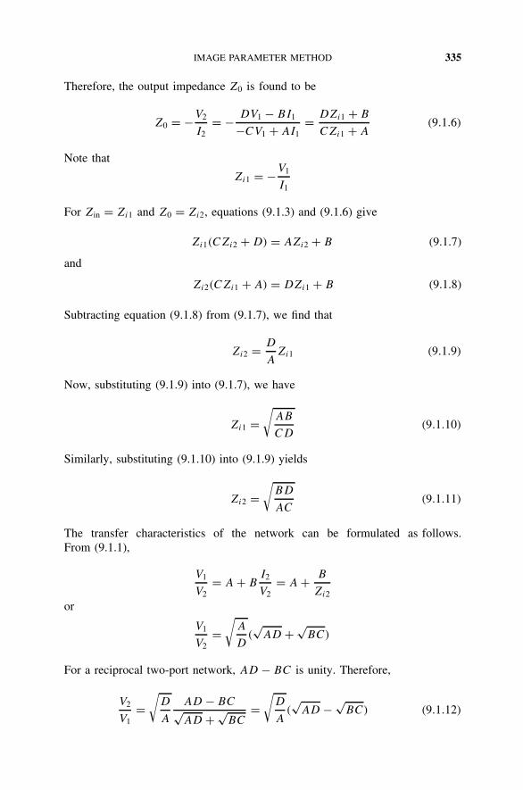
IMAGE PARAMETER METHOD 335
Therefore, the output impedance Z0 is found to be
Z0 = −V2
I2= − DV1 − BI1
−CV1 + AI1= DZi1 + B
CZi1 + A(9.1.6)
Note that
Zi1 = −V1
I1
For Zin = Zi1 and Z0 = Zi2, equations (9.1.3) and (9.1.6) give
Zi1(CZi2 + D) = AZi2 + B (9.1.7)
and
Zi2(CZi1 + A) = DZi1 + B (9.1.8)
Subtracting equation (9.1.8) from (9.1.7), we find that
Zi2 = D
AZi1 (9.1.9)
Now, substituting (9.1.9) into (9.1.7), we have
Zi1 =√
AB
CD(9.1.10)
Similarly, substituting (9.1.10) into (9.1.9) yields
Zi2 =√
BD
AC(9.1.11)
The transfer characteristics of the network can be formulated as follows.From (9.1.1),
V1
V2= A + B
I2
V2= A + B
Zi2
or
V1
V2=
√A
D(√
AD + √BC)
For a reciprocal two-port network, AD − BC is unity. Therefore,
V2
V1=
√D
A
AD − BC√AD + √
BC=
√D
A(√
AD − √BC) (9.1.12)

336 FILTER DESIGN
Similarly, from (9.1.2),
I2
I1=
√A
D(√
AD − √BC) (9.1.13)
Note that equation (9.1.12) is similar to (9.1.13) except that the multiplying coef-ficient in one is the reciprocal of the other. This coefficient may be interpretedas the transformer turns ratio. It is unity for symmetrical T and π networks. Thepropagation factor γ (equal to α + jβ, as usual) of the network can be defined as
e−γ = √AD − √
BC
Since AD − BC = 1, we find that
cosh γ = √AD (9.1.14)
The characteristic parameters of π and T networks are summarized in Table 9.1;the corresponding low-pass and high-pass circuits are given in Table 9.2.
TABLE 9.1 Parameters of T and π Networks
π-Network T-Network
2Z2 2Z2
Z1
Z2
Z1/2 Z1/2
ABCD parameters A = 1 + Z1
2Z2
B = Z1
C = 1
Z2+ Z1
4Z22
D = 1 + Z1
2Z2
A = 1 + Z1
2Z2
B = Z1 + Z21
4Z2
C = 1
Z2
D = 1 + Z1
2Z2
Image impedance Ziπ =√
Z1Z2
1 + Z1/4Z2= Z1Z2
ZiTZiT =
√Z1Z2
(1 + Z1
4Z2
)
Propagation constant, γ cosh γ = 1 + Z1
2Z2cosh γ = 1 + Z1
2Z2

IMAGE PARAMETER METHOD 337
TABLE 9.2 Constant-k Filter Sections
Filter Type T-Section π-Section
Low-pass
C
L /2 L /2 L
C/2 C/2
High-pass
L
2C 2C C
2L2L
For a low-pass T-section as illustrated in Table 9.2,
Z1 = jωL (9.1.15)
and
Z2 = 1
jωC(9.1.16)
Therefore, its image impedance can be found from Table 9.1 as follows:
ZiT =√
L
C
(1 − ω2LC
4
)(9.1.17)
In the case of a dc signal, the second term inside the parentheses will be zeroand the resulting image impedance is generally known as the nominal impedance,Z0. Hence,
Z0 =√
L
C
Note that the image impedance goes to zero if ω2LC/4 = 1. The frequency thatsatisfies this condition is known as the cutoff frequency, ωc. Hence,
ωc = 2√LC
(9.1.18)

338 FILTER DESIGN
Similarly, for a high-pass T-section,
Z1 = 1
jωC(9.1.19)
and
Z2 = jωL (9.1.20)
Therefore, its image impedance is found to be
ZiT =√
L
C
(1 − 1
4ω2LC
)(9.1.21)
The cutoff frequency of this circuit will be given as
ωc = 1
2√
LC(9.1.22)
Example 9.1 Design a low-pass constant-k T-section that has a nominal imped-ance of 75 and a cutoff frequency of 2 MHz. Plot its frequency response in thefrequency band 100 kHz to 10 MHz.
SOLUTION Since the nominal impedance Z0 must be 75 ,
Z0 = 75 =√
L
C
The cutoff frequency ωc of a low-pass T-section is given by (9.1.18). Therefore,
ωc = 2π × 2 × 106 = 2√LC
These two equations can be solved for the inductance L and capacitance C,as follows:
L = 11.9366 µH
and
C = 2.122 nF
This circuit is illustrated in Figure 9.2. Note that inductance L calculated here istwice the value needed for a T-section. Propagation constant γ of this circuit is

IMAGE PARAMETER METHOD 339
5.9683 µH 5.9683 µH
2.122 nF
Figure 9.2 Low-pass constant-k T-section.
0.1 0.2 0.5 1 2 5 10
Frequency (MHz)
−175
−150
−125
−100
−75
−50
−25
Phas
e (d
eg)
0.1 0.2 0.5 1 2 5 10
0.1 0.2 0.5 1 2 5 10
Frequency (MHz)
−40
−30
−20
−10
0
Mag
nitu
de (
dB)
0.1 0.2 0.5 1 2 5 10
Figure 9.3 Frequency response of the T-section shown in Figure 9.2.
determined from the formula listed in Table 8.1. The transfer characteristics arethen found as e−γ.
The frequency response of the designed circuit is shown in Figure 9.3.The magnitude of the transfer function (ratio of the output to input voltages)remains constant at 0 dB for frequencies lower than 2 MHz. Therefore, the

340 FILTER DESIGN
output magnitude will be equal to the input in this range. It falls by 3 dB ifthe signal frequency approaches 2 MHz. It falls continuously as the frequencyincreases further. Note that the phase angle of the transfer function remainsconstant at −180 beyond 2 MHz. However, it shows a nonlinear characteristicin the passband.
The image impedance ZiT of this T-section can be found from (9.1.17). Itscharacteristics (magnitude and phase angle) with frequency are displayed inFigure 9.4. The magnitude of ZiT reduces continuously as frequency is increasedand becomes zero at the cutoff. The phase angle of ZiT is zero in passband, andit changes to 90 in the stopband. Thus, image impedance is a variable resistancein the passband, whereas it switches to an inductive reactance in the stopband.
The frequency characteristics illustrated in Figures 9.3 and 9.4 are representa-tive of any constant-k filter. There are two major drawbacks to this type of filter:
1. The signal attenuation rate after the cutoff point is not very sharp,2. The image impedance is not constant with frequency. From a design point
of view, it is important that it stay constant, at least in its passband.
4 6 8 10
50
100
150
200
250
300
350
2 4 6 8 10
20
40
60
80
Frequency (MHz)
Mag
nitu
de (
Ω)
Frequency (MHz)
2
Figure 9.4 Image impedance of the constant-k filter of Figure 9.2 as a function offrequency.

IMAGE PARAMETER METHOD 341
These problems can be remedied using the techniques described in the follow-ing section.
m-Derived Filter Sections
Consider the two T-sections shown in Figure 9.5. The first network representsthe constant-k filter considered in the preceding section, and the second is anew m-derived section. It is assumed that the two networks have the sameimage impedance. From Table 9.1 we can write
Z′iT = ZiT =
√Z′
1Z′2
(1 + Z′
1
4Z′2
)=
√Z1Z2
(1 + Z1
4Z2
)
It can be solved for Z′2 as follows:
Z′2 = 1
Z′1
(Z1Z2 + Z2
1 − Z′21
4
)(9.1.23)
Now assume thatZ′
1 = mZ1 (9.1.24)
Substituting (9.1.24) in to (9.1.23), we get
Z′2 = Z2
m+ 1 − m2
4 mZ1 (9.1.25)
Thus, an m-derived section is designed from the values of components determinedfor the corresponding constant-k filter. The value of m is selected to sharpenthe attenuation at cutoff or to control the image impedance characteristics inthe passband.
Z1/2 Z1/2
Z2
(a)
Z′1/2
(b)
Z′1/2
Z′2
Figure 9.5 Constant-k T-section (a) and m-derived section (b).

342 FILTER DESIGN
For a low-pass filter, the m-derived section can be designed from the corre-sponding constant-k filter using (9.1.24) and (9.1.25) as follows:
Z′1 = jωmL (9.1.26)
and
Z′2 = 1 − m2
4 mjωL + 1
jωmC(9.1.27)
Now we need to find its propagation constant γ and devise some way to controlits attenuation around the cutoff. Expression for the propagation constant of a T-section is listed in Table 9.1. To find γ of this T-section, we first divide (9.1.26)by (9.1.27):
Z′1
Z′2
= − ω2m2LC
1 − [(1 − m2)/4]ω2LC= − 4ω2m2/ω2
c
1 − (1 − m2)ω2/ω2c
(9.1.28)
where
ωc = 2√LC
(9.1.29)
Using the formula listed in Table 9.1 and (9.1.28), the propagation constant γ isfound as follows:
cosh γ = 1 + Z′1
2Z′2
= 1 − 2 (mω/ωc)2
1 − (1 − m2) (ω/ωc)2
or
cosh γ = ω2c − ω2 − (mω)2
ω2c − (1 − m2)ω2
(9.1.30)
Hence, the right-hand side of (9.1.30) is dependent on the frequency ω. It willgo to infinity (and therefore, γ) if the following condition is satisfied:
ω = ωc√1 − m2
= ω∞ (9.1.31)
This condition can be used to sharpen the attenuation at cutoff. A small m willplace ω∞ close to ω. In other words, ω∞ is selected a little higher than ωc andthe fractional value of m is then determined from (9.1.31). Z′
1 and Z′2 of the m-
derived section are subsequently found using (9.1.24) and (9.1.25), respectively.Note that the image impedance of an m-derived T-section is the same as
that of the corresponding constant-k network. However, it will be a function ofm in the case of a π-network. Therefore, this characteristic can be utilized todesign input and output networks of the filter so that the image impedance ofthe composite circuit stays almost constant in its passband. Further, an infinitecascade of T-sections can be considered as a π-network after splitting its shunt
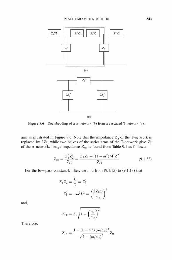
IMAGE PARAMETER METHOD 343
Z1′/2 Z1′/2 Z1′/2 Z1′/2
(a)
Z2′ Z2′
Z1′
(b)
2Z2′ 2Z2′
Figure 9.6 Deembedding of a π-network (b) from a cascaded T-network (a).
arm as illustrated in Figure 9.6. Note that the impedance Z′2 of the T-network is
replaced by 2Z′2, while two halves of the series arms of the T-network give Z′
1of the π-network. Image impedance Ziπ is found from Table 9.1 as follows:
Ziπ = Z′1Z
′2
ZiT= Z1Z2 + [(1 − m2)/4]Z2
1
ZiT(9.1.32)
For the low-pass constant-k filter, we find from (9.1.15) to (9.1.18) that
Z1Z2 = L
C= Z2
0
Z21 = −ω2L2 =
(2Z0ω
ωc
)2
and,
ZiT = Z0
√1 −
(ω
ωc
)2
Therefore,
Ziπ = 1 − (1 − m2) (ω/ωc)2√
1 − (ω/ωc)2
Z0

344 FILTER DESIGN
Normalized frequency
Nor
mal
ized
impe
danc
e
m = 0.4
m = 0.6
m = 0.8
2.5
2.0
1.5
1.0
0.50.0 0.2 0.4 0.6 0.8 1.0
Figure 9.7 Normalized image impedance of π-network versus normalized frequency forthree values of m.
or
Ziπ = 1 − (1 − m2)ω2√(1 − ω2)
(9.1.33)
where Ziπ = Ziπ/Z0 may be called the normalized image impedance of a π-network and ω = ω/ωc the normalized frequency.
Equation (9.1.33) is displayed graphically in Figure 9.7. The normalized imageimpedance is close to unity for nearly 90% of the passband if m is kept around0.6. Therefore, it can be used as pre- and poststages of the composite filter (afterbisecting it) to control the input impedance. These formulas will be developedlater in this section.
Example 9.2 Design an m-derived T-section low-pass filter with a cutoff fre-quency of 2 MHz and a nominal impedance of 75 . Assume that f∞ = 2.05 MHz.Plot the response of this filter in the frequency band of 100 kHz to 10 MHz.
SOLUTION From (9.1.31),
1 − m2 =(
fc
f∞
)2
Therefore,
m =√
1 −(
fc
f∞
)2
=√
1 −(
2
2.05
)2
= 0.2195
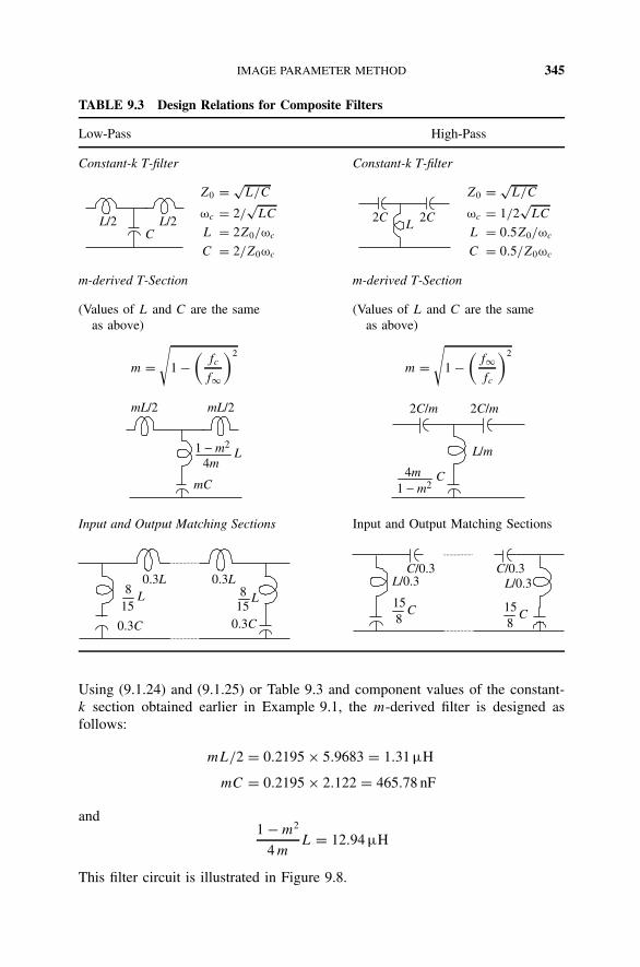
IMAGE PARAMETER METHOD 345
TABLE 9.3 Design Relations for Composite Filters
Low-Pass High-Pass
Constant-k T-filter Constant-k T-filter
L/2 L/2 C
Z0 = √L/C
ωc = 2/√
LC
L = 2Z0/ωc
C = 2/Z0ωc
L 2C2C
Z0 = √L/C
ωc = 1/2√
LC
L = 0.5Z0/ωc
C = 0.5/Z0ωc
m-derived T-Section m-derived T-Section
(Values of L and C are the same (Values of L and C are the sameas above) as above)
m =√
1 −(
fc
f∞
)2
m =√
1 −(
f∞fc
)2
mC
mL/2 mL/2
L4m
1 − m2
C4m
2C/m 2C/m
1 − m2
L/m
Input and Output Matching Sections Input and Output Matching Sections
0.3L 0.3L L
158
0.3C 0.3C
L158
C815
C/0.3 C/0.3 L/0.3 L/0.3
C815
Using (9.1.24) and (9.1.25) or Table 9.3 and component values of the constant-k section obtained earlier in Example 9.1, the m-derived filter is designed asfollows:
mL/2 = 0.2195 × 5.9683 = 1.31 µH
mC = 0.2195 × 2.122 = 465.78 nF
and1 − m2
4 mL = 12.94 µH
This filter circuit is illustrated in Figure 9.8.

346 FILTER DESIGN
1.31 µH 1.31 µH
12.94 µH
465.78 pF
Figure 9.8 An m-derived T-section for Example 9.2.
As noted earlier, the image impedance of this circuit will be the same as thatof the corresponding constant-k section. Hence, it will vary with frequency asillustrated in Figure 9.4. The propagation constant γ of this circuit is determinedfrom the formula listed in Table 9.1. The transfer characteristics are then foundas e−γ. Its magnitude and phase characteristics versus frequency are illustrated inFigure 9.9. The transfer characteristics illustrated in Figure 9.9 indicate that them-derived filter has a sharp change at a cutoff frequency of 2 MHz. However, theoutput signal rises to −4 dB in its stopband. On the other hand, the constant-kfilter provides higher attenuation in its stopband. For example, the m-derivedfilter characteristic in Figure 9.9 shows only 4-dB attenuation at 6 MHz, whereasthe corresponding constant-k T-section has an attenuation of more than 30 dB atthis frequency, as depicted in Figure 9.3.
Composite Filters
As demonstrated through the preceding examples, the m-derived filter providesan infinitely sharp attenuation right at its cutoff. However, the attenuation inits stopband is unacceptably low. Contrary to this, the constant-k filter shows ahigher attenuation in its stopband, although the change is unacceptably gradualat the transition from passband to stopband. One way to solve the problem is tocascade these two filters. Since image impedance stays the same in two cases,this cascading will not create a new impedance-matching problem. However, westill need to address the problem of image impedance variation with frequencyat the input and output ports of the network.
As illustrated in Figure 9.7, the image impedance of the π-section with m =0.6 remains almost constant over 90% of the passband. If this network is bisectedto connect on either side of the cascaded constant-k and m-derived sections,it should provide the desired impedance characteristics. To verify these char-acteristics, let us consider a bisected π-section as shown in Figure 9.10. Itstransmission parameters can be found easily following the procedure describedin Chapter 8.
From (8.4.4) to (8.4.7), we find that
A = 1 + Z′1
4Z′2
(9.1.34)

IMAGE PARAMETER METHOD 347
−175
−150
−125
−100
−75
−50
−25
0
0.1 0.2 0.5 1 2 5 10
Frequency (MHz)
0.1 0.2 0.5 1 2 5 10
Frequency (MHz)
−10
−8
−6
−4
−2
00.1 0.2 0.5 1 2 5 10
0.1 0.2 0.5 1 2 5 10
Mag
nitu
de (
dB)
Phas
e (d
eg)
Figure 9.9 Frequency response of the m-derived T-section shown in Figure 9.8.
Z ′1/2
2Z ′2 Zi1 Zi2
Figure 9.10 Right-hand side of the bisected π-section shown in Figure 9.6.

348 FILTER DESIGN
B = Z′1
2(9.1.35)
C = 1
2Z′2
(9.1.36)
and
D = 1 (9.1.37)
Image impedance Zi1 and Zi2 can now be found from (9.1.10) and (9.1.11)as follows:
Zi1 =√
Z′1Z
′2 + Z
′21
4= ZiT (9.1.38)
and
Zi2 =√
Z′1Z
′2
1 + Z′1/4Z′
2
= Z′1Z
′2
ZiT= Ziπ (9.1.39)
Thus, the bisected π-section can be connected at the input and output portsof cascaded constant-k and m-derived sections to obtain a composite filter thatsolves the impedance problem as well. Relations for the design of these circuitsare summarized in Table 9.3.
Example 9.3 Design a low-pass composite filter with a cutoff frequency of2 MHz and an image impedance of 75 in its passband. Assume that f∞ =2.05 MHz. Plot its response in the frequency range 100 kHz to 10 MHz.
SOLUTION Constant-k and m-derived sections of this filter are designed inExamples 9.1 and 9.2, respectively. The filter’s input and output matching sec-tions can be designed as follows. With m = 0.6, we find that
mL
2= 3.581 µH
mC
2= 636.6 pF
and
1 − m2
2 mL = 6.366 µH
This composite filter is depicted in Figure 9.11.Figure 9.12 illustrates the frequency response of this composite filter. As it
indicates, there is a fairly sharp change in output signal as the frequency changesfrom its passband to the stopband. At the same time, the output stays well below−40 dB in its stopband. Figure 9.13 shows variation in the image impedance

IMAGE PARAMETER METHOD 349
2.122 nF 465.78 pF
3.581 µH
6.366 µH
636.6 pF
5.9683 µH 5.9683 µH 12.94 µH
636.6 pF
6.366 µH
1.31 µH 1.31 µH 3.581 µH
Bisected Π Bisected ΠConstant-k m-derived
Figure 9.11 Composite filter of Example 9.3.
150
100
50
−50
−100
−150
0
0.1 0.2 0.5 1 2 5 10
Frequency (MHz)
0.1 0.2 0.5 1 2 5 10
Frequency (MHz)
−50
−40
−30
−20
−10
00.1 0.2 0.5 1 2 5 10
0.1 0.2 0.5 1 2 5 10
Mag
nitu
de (
dB)
Phas
e (d
eg)
Figure 9.12 Frequency response of the composite filter of Figure 9.11.

350 FILTER DESIGN
1 2 3 4
50
100
150
200
Frequency (MHz)
Mag
nitu
de (
Ω)
Phas
e (d
eg)
1 2 3 4
−75
−50
−25
25
50
75
Frequency (MHz)
Figure 9.13 Image impedance of the composite filter of Figure 9.11 versus frequency.
of this filter as the signal frequency changes. This indicates that the imageimpedance stays at 75 (pure real, because the phase angle is zero) over mostof its passband.
Example 9.4 Design a high-pass composite filter with a nominal impedance of75 . It must pass all signals over 2 MHz. Assume that f∞ = 1.95 MHz. Plot itscharacteristics in the frequency range 1 to 10 MHz.
SOLUTION From Table 9.3, we find the components of its constant-k sectionas follows:
L = 75
2 × 2 × π × 2 × 10⁶H = 2.984 µH
and
C = 1
2 × 2 × π × 2 × 106 × 75F = 530.5 pF

IMAGE PARAMETER METHOD 351
Similarly, the component values for its m-derived filter section are determinedas follows:
m =√
1 −(
f∞fc
)2
=√
1 −(
1.95
2
)2
= 0.222
Hence,
2C
m= 4.775 nF
L
m= 13.43 µH
and4 m
1 − m2C = 0.496 nF
The component values for the bisected π-section to be used at its input andoutput ports are found as
C
0.3= 1.768 nF
L
0.3= 9.947 µH
and15
8C = 0.9947 nF
The composite filter (after simplifying for the series capacitors in various sections)is illustrated in Figure 9.14.
The frequency response of this composite filter is depicted in Figure 9.15. Itshows that the attenuation in its stopband stays below −40 dB, and the switchingto passband is fairly sharp. As usual with this type of circuit, its phase characteris-tics may not be acceptable for certain applications because of inherent distortion.
0.6631 nF
9.947 µH 9.947 µH 2.984 µH 13.43 µH
0.8681 nF 1.2903 nF
0.9947 nF 0.496 nF 0.9947 nF
Figure 9.14 Composite high-pass filter with 2-MHz cutoff frequency.
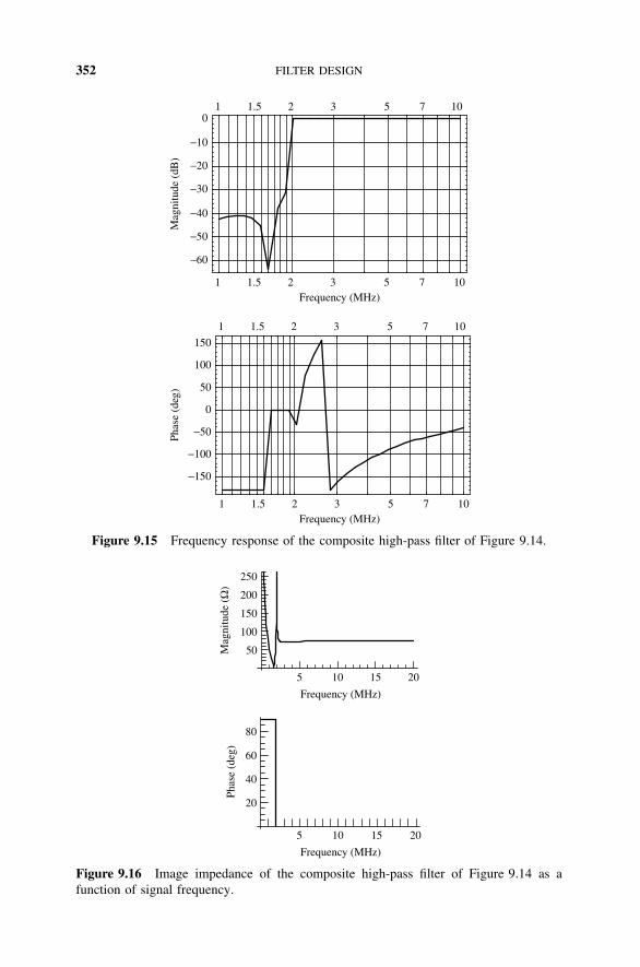
352 FILTER DESIGN
−150
−100
−50
0
50
100
150
1 1.5 2 3 5 7 10Frequency (MHz)
1 1.5 2 3 5 7 10Frequency (MHz)
−60
−50
−40
−30
−20
−10
0
Mag
nitu
de (
dB)
Phas
e (d
eg)
1 1.5 2 3 5 7 10
1 1.5 2 3 5 7 10
Figure 9.15 Frequency response of the composite high-pass filter of Figure 9.14.
5 10 15 20
50
100
150
200
250
5 10 15 20
20
40
60
80
Frequency (MHz)
Frequency (MHz)
Mag
nitu
de (
Ω)
Phas
e (d
eg)
Figure 9.16 Image impedance of the composite high-pass filter of Figure 9.14 as afunction of signal frequency.

INSERTION-LOSS METHOD 353
As depicted in Figure 9.16, the image impedance of this composite filter isalmost constant at 75 . Note that its magnitude varies over a wide range in thestopband while its phase angle seems to remain constant at 90. The phase angleof the image impedance is zero in the passband.
9.2 INSERTION-LOSS METHOD
The output of an ideal filter would be the same as its input in the passband,whereas it would be zero in the stopband. The phase response of this filter mustbe linear to avoid signal distortion. In reality, such circuits do not exist and a com-promise is needed to design the filters. The image parameter method describedin Section 9.1 provides a simple design procedure. However, the transfer char-acteristics of this circuit cannot be shaped as desired. On the other hand, theinsertion-loss method provides ways to shape pass- and stopbands of the filter,although its design theory is much more complex.
The power-loss ratio of a two-port network is defined as the ratio of the powerthat is delivered to the load when it is connected directly at the generator to thepower delivered when the network is inserted between the two. In other words,
PLR = power incident at port 1
power delivered to the load connected at port 2= 1
1 − |(ω)|2(9.2.1)
The power-loss ratio, PLR, expressed in decibels, is generally known as the inser-tion loss of the network. It can be proved that |(ω)|2 must be an even function ofω for a physically realizable network. Therefore, polynomials of ω2 can representit as follows.
|(ω)|2 = f1(ω2)
f1(ω2) + f2(ω2)(9.2.2)
and
PLR = 1 + f1(ω2)
f2(ω2)(9.2.3)
where f1(ω2) and f2(ω
2) are real polynomials in ω2.Alternatively, the magnitude of the voltage gain of the two-port network can
be found as
|G(ω)| = 1√PLR
= 1√1 + f1(ω2)/f2(ω2)
(9.2.4)
Hence, if PLR is specified, (ω) is fixed. Therefore, the insertion-loss method issimilar to the impedance-matching methods discussed in Chapter 7.
Traditionally, the filter design begins with a lumped-element low-pass networkthat is synthesized by using normalized tables. It is subsequently scaled to thedesired cutoff frequency and the impedance. Also, the low-pass prototype can

354 FILTER DESIGN
ωc0
Passband Stopband
G
(ω)
1
ω
Figure 9.17 Characteristics of an ideal low-pass filter.
be transformed to obtain a high-pass, a bandpass, or a bandstop filter. Theselumped-element filters are used as a starting point to design the transmission linefilter. In this section we present the design procedure for two different types oflumped-element low-pass filters. It is followed by the transformation techniquesused to design high-pass, bandpass, and bandstop filters.
Low-Pass Filters
As illustrated in Figure 9.17, an ideal low-pass filter will pass the signals belowits cutoff frequency ωc without attenuation while it will stop those with higherfrequencies. Further, the transition from its passband to its stopband will be sharp.In reality, this type of filter cannot be designed. Several approximations to thesecharacteristics are available that can be physically synthesized. Two of these arepresented below.
Maximally Flat Filter
As its name suggests, this type of filter provides the flattest possible passbandresponse. However, its transition from passband to stopband is gradual. This isalso known as a binomial or Butterworth filter. The magnitude of its voltage gain(and hence, its frequency response) is given as follows:
|G(ω)| = 1√1 + ζω2n
n = 1, 2, 3, . . . (9.2.5)
where ζ is a constant that controls the power-loss ratio at its band edge, n is theorder, and ω is the normalized frequency. For |G(ω)| = 0.7071 (i.e., −3 dB) atthe band edge, ζ is unity.
Note that derivatives of |G(ω)| at normalized frequencies much below theband edge are close to zero. This guarantees maximum flatness in the passband.Further, (9.2.5) indicates that |G(ω)| will be a fractional number for ω greaterthan zero. Therefore, it is generally known as the insertion loss, L, of the networkwhen expressed in decibels. Hence,
L = −20 log10
[1√
1 + ζ (ω/ωc)2n
]= 10 log10
[1 + ζ
(ω
ωc
)2n]
dB
(9.2.6)

INSERTION-LOSS METHOD 355
0.8 1 1.2
−2.5
−2
−1.5
−1
−0.5
Normalized frequency
G(ω
)(d
B)
n = 2
n = 4
n = 7
0.2 0.4 0.6
Figure 9.18 Characteristics of maximally flat low-pass filters.
orL
10= log10
[1 + ζ
(ω
ωc
)2n]
or
ζ
(ω
ωc
)2n
= 10L/10 − 1 (9.2.7)
Figure 9.18 illustrates the passband characteristics of this type of filter forthree different values of n. The power-loss ratio at its band edge is assumed tobe −3 dB, and therefore ζ is equal to unity. It shows that the passband becomesflatter with a sharper cutoff when its order n is increased. However, this rela-tionship is not a linear one. This change in characteristics is significant for lowervalues of n.
Equation (9.2.7) can be used for determining the ζ and n values of a filteras follows. If the insertion loss at the band edge (ω = ωc) is specified as L =Lc, (9.2.7) yields
ζ = 10Lc/10 − 1 (9.2.8)
Similarly, the required order n (and hence, number of elements required) of afilter can be determined for the L specified at a given stopband frequency. It isfound as follows:
n = 1
2× log10(10L/10 − 1) − log10 ζ
log10 (ω/ωc)(9.2.9)
Chebyshev Filter
A filter with a sharper cutoff can be realized at the cost of flatness in its passband.Chebyshev filters possess ripples in the passband but provide a sharp transition
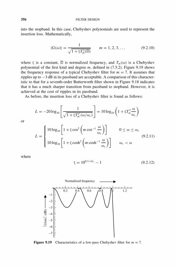
356 FILTER DESIGN
into the stopband. In this case, Chebyshev polynomials are used to represent theinsertion loss. Mathematically,
|G(ω)| = 1√1 + ζT 2
m(ω)m = 1, 2, 3, . . . (9.2.10)
where ζ is a constant, ω is normalized frequency, and Tm(ω) is a Chebyshevpolynomial of the first kind and degree m, defined in (7.5.2). Figure 9.19 showsthe frequency response of a typical Chebyshev filter for m = 7. It assumes thatripples up to −3 dB in its passband are acceptable. A comparison of this character-istic to that for a seventh-order Butterworth filter shown in Figure 9.18 indicatesthat it has a much sharper transition from passband to stopband. However, it isachieved at the cost of ripples in its passband.
As before, the insertion loss of a Chebyshev filter is found as follows:
L = −20 log10
[1√
1 + ζT 2m (ω/ωc)
]= 10 log10
(1 + ζT 2
m
ω
ωc
)or
L =
10 log10
[1 + ζ cos2
(m cos−1 ω
ωc
)]0 ≤ ω ≤ ωc
10 log10
[1 + ζ cosh2
(m cosh−1 ω
ωc
)]ωc < ω
(9.2.11)
where
ζ = 100.1×Gr − 1 (9.2.12)
0.2 0.6 1 1.2
−7
−6
−5
−4
−3
−2
−1
Normalized frequency
0.80.4
G(ω
) (d
B)
Figure 9.19 Characteristics of a low-pass Chebyshev filter for m = 7.

INSERTION-LOSS METHOD 357
Gr is the ripple amplitude in decibels. The order m (and hence, number of ele-ments) of a Chebyshev filter can be found from its characteristics as follows:
m = cosh−1√
(100.1×L − 1)/(100.1×Gr − 1)
cosh−1(ω/ωc)(9.2.13)
where L is required insertion loss in decibels at a specified frequency ω.
Example 9.5 It is desired to design a maximally flat low-pass filter with at least15 dB attenuation at ω = 1.3 ωc and −3 dB at its band edge. How many elementswill be required for this filter? If a Chebyshev filter is used with a 3-dB ripplein its passband, find the number of circuit elements.
SOLUTION From (9.2.8),
ζ = 10Lc/10 − 1 = 100.3 − 1 = 1
and from (9.2.9) we have
n = 1
2× log10(10L/10 − 1) − log10 ζ
log10(ω/ωc)= 0.5 × log10(101.5 − 1)
log10(1.3)= 6.52
Therefore, seven elements will be needed for this maximally flat filter.In the case of a Chebyshev filter, (9.2.13) gives
m = cosh−1√
(100.1×L − 1)/(100.1×Gr − 1)
cosh−1(ω/ωc)= cosh−1
√101.5 − 1
cosh−1(1.3)= 3.17
Hence, it will require only three elements. The characteristics of these two filtersare illustrated in Figure 9.20.
0.5 1 1.5 2
−7
−6
−5
−4
−3
−2
−1
Normalized frequency
G(ω
) (d
B)
Figure 9.20 Characteristics of low-pass Butterworth and Chebyshev filters.

358 FILTER DESIGN
Low-Pass Filter Synthesis
The scope of this book does not include the theory of passive filter synthesis.Several excellent references are available in the literature for those who maybe interested in this. The design procedure presented here is based on a doublyterminated low-pass ladder network, as shown in Figure 9.21. The g notation usedin the figure signifies the roots of an nth-order transfer function that govern itscharacteristics. These represent the normalized reactance values of filter elementswith a cutoff frequency ωc = 1. The source resistance is represented by g0, andthe load is gn+1. The filter is made up of series inductors and shunt capacitorsthat are in the form of cascaded T-networks. Another possible configuration isthe cascaded π-network that is obtained after replacing g1 by a short circuit,connecting a capacitor across the load gn+1, and renumbering filter elements1 through n. Elements of this filter are determined from the n roots of thetransfer function.
The transfer function is selected according to the pass- and stopband charac-teristics desired. Normalized values of elements are then found from the rootsof that transfer function. These values are then adjusted according to the desiredcutoff frequency and the source and load resistance. Design procedures for themaximally flat and the Chebyshev filters can be summarized as follows.
Assume that the cutoff frequency is given as follows:
ωc = 1 (9.2.14)
Butterworth and Chebyshev filters can then be designed using the followingformulas.
For a Butterworth filter,
g0 = gn+1 = 1 (9.2.15)
and
gp = 2 sin(2p − 1)π
2np = 1, 2, · · · , n (9.2.16)
Element values computed from (9.2.15) and (9.2.16) are given in Table 9.4 forn up to 7.
g0
g1 g3 g5
g4g2
gngn−2
gn−1 gn+1
Figure 9.21 Low-pass ladder network prototype.

INSERTION-LOSS METHOD 359
TABLE 9.4 Element Values for Low-Pass Binomial Filter Prototypes (g0 = 1,ωc = 1)
n g1 g2 g3 g4 g5 g6 g7 g8
1 2.0000 1.00002 1.4142 1.4142 13 1.0000 2.0000 1.0000 1.00004 0.7654 1.8478 1.8478 0.7654 1.00005 0.6180 1.6180 2.0000 1.6180 0.6180 16 0.5176 1.4142 1.9319 1.9319 1.4142 0.5176 17 0.4450 1.2470 1.8019 2.0000 1.8019 1.2470 0.445 1.0000
For a Chebyshev filter,
g0 = 1 (9.2.17)
gm+1 =
1 m is an odd number
cothξ
4m is an even number
(9.2.18)
g1 = 2a1
χ(9.2.19)
and
gp = 4a(p−1)ap
b(p−1)g(p−1)
p = 2, 3, · · · , m (9.2.20)
where
ξ = ln
(coth
Gr
17.37
)(9.2.21)
χ = sinhξ
2 m(9.2.22)
ap = sin(2p − 1)π
2 m(9.2.23)
and
bp = χ2 + sin2 pπ
m(9.2.24)
The element values for several low-pass Chebyshev filters that are computedfrom (9.2.17) to (9.2.24) are given in Tables 9.5 to 9.9.

360 FILTER DESIGN
TABLE 9.5 Element Values for Low-Pass Chebyshev Filter Prototypes (g0 = 1,ωc = 1, and 0.1 dB ripple)
m g1 g2 g3 g4 g5 g6 g7 g8
1 0.3053 1.0002 0.8431 0.6220 1.35543 1.0316 1.1474 1.0316 1.00004 1.1088 1.3062 1.7704 0.8181 1.35545 1.1468 1.3712 1.9750 1.3712 1.1468 1.00006 1.1681 1.4040 2.0562 1.5171 1.9029 0.8618 1.35547 1.1812 1.4228 2.0967 1.5734 2.0967 1.4228 1.1812 1.0000
TABLE 9.6 Element Values for Low-Pass Chebyshev Filter Prototypes (g0 = 1,ωc = 1, and 0.5 dB ripple)
m g1 g2 g3 g4 g5 g6 g7 g8
1 0.6987 1.00002 1.4029 0.7071 1.98413 1.5963 1.0967 1.5963 1.00004 1.6703 1.1926 2.3662 0.8419 1.98415 1.7058 1.2296 2.5409 1.2296 1.7058 1.00006 1.7254 1.2479 2.6064 1.3136 2.4759 0.8696 1.98417 1.7373 1.2582 2.6383 1.3443 2.6383 1.2582 1.7373 1.0000
TABLE 9.7 Element Values for Low-Pass Chebyshev Filter Prototypes (g0 = 1,ωc = 1, and 1.0 dB ripple)
m g1 g2 g3 g4 g5 g6 g7 g8
1 1.0178 1.00002 1.8220 0.6850 2.65993 2.0237 0.9941 2.0237 1.00004 2.0991 1.0644 2.8312 0.7892 2.65995 2.1350 1.0911 3.0010 1.0911 2.1350 1.00006 2.1547 1.1041 3.0635 1.1518 2.9368 0.8101 2.65997 2.1666 1.1115 3.0937 1.1735 3.0937 1.1115 2.1666 1.0000
Scaling the Prototype to the Desired Cutoff Frequency and Load
ž Frequency scaling. For scaling the frequency from 1 to ωc, divide all nor-malized g values that represent capacitors or inductors by the desired cutofffrequency expressed in radians per second. Resistors are excluded fromthis operation.

INSERTION-LOSS METHOD 361
TABLE 9.8 Element Values for Low-Pass Chebyshev Filter Prototypes (g0 = 1,ωc = 1, and 2.0 dB ripple)
m g1 g2 g3 g4 g5 g6 g7 g8
1 1.5297 1.00002 2.4883 0.6075 4.09573 2.7108 0.8326 2.7108 1.00004 2.7926 0.8805 3.6064 0.6818 4.09575 2.8311 0.8984 3.7829 0.8984 2.8311 1.00006 2.8522 0.9071 3.8468 0.9392 3.7153 0.6964 4.09577 2.8651 0.9120 3.8776 0.9536 3.8776 0.9120 2.8651 1.0000
TABLE 9.9 Element Values for Low-Pass Chebyshev Filter Prototypes (g0 = 1,ωc = 1, and 3.0 dB ripple)
m g1 g2 g3 g4 g5 g6 g7 g8
1 1.9954 1.00002 3.1014 0.5339 5.80953 3.3489 0.7117 3.3489 1.00004 3.4391 0.7483 4.3473 0.5920 5.80955 3.4815 0.7619 4.5378 0.7619 3.4815 1.00006 3.5047 0.7685 4.6063 0.7929 4.4643 0.6033 5.80957 3.5187 0.7722 4.6392 0.8038 4.6392 0.7722 3.5187 1.0000
ž Impedance scaling. To scale g0 and gn+1 to X from unity, multiply allg values that represent resistors or inductors by X. On other hand, dividethose g values representing capacitors by X.
Example 9.6 Design a Butterworth filter with a cutoff frequency of 10 MHzand an insertion loss of 30 dB at 40 MHz. It is to be used between a 50- loadand a generator with an internal resistance of 50 .
SOLUTION From (9.2.9), we have
n = 1
2× log10(1030/10 − 1) − log10(103/10 − 1)
log10(40/10)
= 1
2× log10(103 − 1) − log10(1.9953 − 1)
log10(4)≈ 0.5 × 3
0.6≈ 2.5
Since the number of elements must be an integer, selecting n = 3 will providemore than the attenuation specified at 40 MHz. From (9.2.15) and (9.2.16),
g0 = g4 = 1

362 FILTER DESIGN
50 Ω
50 Ω795.77 nH 795.77 nH
636.62 pF
L1 L3
C2
R0 = RsR4 = RL
Figure 9.22 Maximally flat low-pass filter obtained in Example 9.6.
g1 = 2 sinπ
6= 1
g2 = 2 sinπ
2= 2
and
g3 = 2 sin5π
6= 1
If we use the circuit arrangement illustrated in Figure 9.22, element values canbe scaled to match the frequency and load resistance. Using the two rules, thesevalues are found as follows:
L1 = L3 = 50 × 1
2π × 107H = 795.77 nH
and
C2 = 1
50× 2
2π × 107F = 636.62 pF
The frequency response of this filter is shown in Figure 9.23. It indicates a 6-dB insertion loss in the passband of the filter. This happens because the sourceresistance is considered a part of this circuit. In other words, this representsvoltage across RL with respect to source voltage, not to input of the circuit. Sincesource resistance is equal to the load, there is equal division of source voltagethat results in −6 dB. Another 3-dB loss at the band edge shows a total of about9 dB at 10 MHz. This characteristic shows that there is an insertion loss of over40 dB at 40 MHz. It is clearly more than 30 dB from the band edge, as requiredby the example. Also, there is a nonlinear phase variation in its passband.
Alternatively, we can use a circuit topology as shown in Figure 9.24. In thatcase, component values are found by using the scaling rules:
L2 = 50 × 1
2π × 107× 2 = 0.15915 × 10⁻⁵ H = 1591.5 nH
and
C1 = C3 = 1
50× 1
2π × 107× 1 = 10−9
πF = 318.31 pF

INSERTION-LOSS METHOD 363
−150
−100
−50
0
50
100
150
−60
−50
−40
Mag
nitu
de (
dB)
Phas
e (d
eg)
−30
−20
−10
00.1 0.5 1 5 10 50 100
0.1 0.5 1 5
Frequency (MHz)
10 50 100
0.1 0.5 1 5 10 50 100
0.1 0.5 1 5
Frequency (MHz)
10 50 100
Figure 9.23 Characteristics of the low-pass filter shown in Figure 9.22.
50 Ω
50 Ω
1.5915 µH
318.31 pF 318.31 pF
C1 C3 R1 = Rs R4 = RL
L2
Figure 9.24 Alternative circuit for Example 9.6.
The frequency response of this circuit is illustrated in Figure 9.25. It is identicalto that shown in Figure 9.23 for the earlier circuit.
Example 9.7 Design a low-pass Chebyshev filter that may have ripples no morethan 0.01 dB in its passband. The filter must pass all frequencies up to 100 MHz

364 FILTER DESIGN
−150
−100
−50
0
50
100
150
−60
Mag
nitu
de (
dB)
Phas
e (d
eg)
−50
−40
−30
−20
−10
00.1 0.5 1 5 10 50 100
0.1 0.5 1 5
Frequency (MHz)
10 50 100
0.1 0.5 1 5 10 50 100
0.1 0.5 1 5
Frequency (MHz)
10 50 100
Figure 9.25 Characteristics of the low-pass filter shown in Figure 9.24.
and attenuate the signal at 400 MHz by at least 5 dB. The load and the sourceresistance are of 75 each.
SOLUTION Since
Gr = 0.01 dB
and
L
(400
100
)= 5 dB
INSERTION-LOSS METHOD 365
(9.2.13) gives
m = cosh−1√
(100.5 − 1)/(100.001 − 1)
cosh−1(4)= 2
Since we want a symmetrical filter with 75 on each side, we select m = 3(an odd number). It will provide more than 5 dB of insertion loss at 400 MHz.The g values can now be determined from (9.2.17) to (9.2.24), as follows. From(9.2.23),
a1 = sinπ
6= 0.5
a2 = sinπ
2= 1
and
a3 = sin5π
6= 0.5
Next, from (9.2.21), (9.2.22), and (9.2.24), we get
ξ = ln
(coth
0.01
17.37
)= 7.5
χ = sinh7.5
6= 1.6019
b1 = 1.60192 + sin2 π
3= 3.316
b2 = 1.60192 + sin2 2π
3= 3.316
and
b3 = 1.60192 + sin2 3π
3= 2.566
However, b3 is not needed in further calculations.Finally, from (9.2.17) and (9.2.20),
g0 = g4 = 1
g1 = 2 × 0.5
1.6019= 0.62425
g2 = 4 × 0.5 × 1
3.316 × 0.62425= 0.9662
and
g3 = 4 × 1 × 0.5
3.316 × 0.9662= 0.62425

366 FILTER DESIGN
75 Ω
75 Ω
74.5155 nH 74.5155 nH
20.5 pF
L1 L3
C2
R0 = RsR4 = RL
Figure 9.26 Low-pass Chebyshev filter circuit obtained in Example 9.7.
For the circuit topology of Figure 9.26, element values are found after applyingthe scaling rules as follows:
L1 = L3 = 75 × 0.62425
2π × 108H = 74.5155 nH
and
C2 = 1
75× 1
2π × 108× 0.9662 F = 20.5 pF
The frequency response of this filter is illustrated in Figure 9.27. As expected,there is over a 20-dB insertion loss at 400 MHz compared with its passband.Note that the magnitude of ripple allowed is so small that it does not show upin this figure. However, it is present there, as shown on an expanded scale inFigure 9.28.
Figure 9.28 shows the passband characteristics of this Chebyshev filter. Sincethe scale-of-magnitude plot is now expanded, the passband ripple is clearly visi-ble. As expected, the ripple stays between −6.02 and −6.03 dB. Phase variationin this passband ranges from 0 to −70. The band edge of this filter can besharpened further either by using a higher-order filter or by allowing larger mag-nitudes of the ripple in its passband. The higher-order filter will require moreelements because the two are directly related. The next example illustrates that asharper transition between the bands can be obtained even with a three-elementfilter if ripple magnitudes up to 3 dB are acceptable.
Example 9.8 Reconsider Example 9.7 to design a low-pass filter that exhibitsthe Chebyshev response with 3-dB ripple in its passband, m = 3, and a cutofffrequency of 100 MHz. The filter must have 75 at both its input and outputports.
SOLUTION From (8.2.23),
a1 = sinπ
6= 0.5
a2 = sinπ
2= 1

INSERTION-LOSS METHOD 367
−150
−100
−50
0
50
100
150
Frequency (MHz)
−50
−40
−30
−20
−10
01 5 10
Mag
nitu
de (
dB)
Phas
e (d
eg)
50 100 500 1000
1 5 10 50 100 500 1000
1 5 10 50 100 500 1000
Frequency (MHz)
1 5 10 50 100 500 1000
Figure 9.27 Characteristics of the low-pass Chebyshev filter shown in Figure 9.26.
and
a3 = sin5π
6= 0.5
Now, from (9.2.21), (9.2.22), and (9.2.24),
ξ = ln
(coth
3
17.37
)= 1.7661
χ = sinh1.7661
6= 0.2986

368 FILTER DESIGN
−60
−50
−40
−30
−20
−10
0
Frequency (MHz)
Frequency (MHz)
−6.03
−6.028
−6.026
−6.024
−6.022
Mag
nitu
de (
dB)
Phas
e (d
eg)
1 2 5 10 20 50 100
1 2 5 10 20 50 100
1 2 5 10 20 50 100
1 2 5 10 20 50 100
Figure 9.28 Passband characteristics of the filter shown in Figure 9.26.
b1 = 0.29862 + sin2 π
3= 0.8392
b2 = 0.29862 + sin2 2π
3= 0.8392
and
b3 = 0.29862 + sin2 3π
3= 0.0892
However, b3 is not needed.

INSERTION-LOSS METHOD 369
75 Ω
75 Ω0.4 µH 0.4 µH
15.1 pF
L1 L3
C2
R0 = RsR4 = RL
Figure 9.29 Low-pass Chebyshev filter circuit obtained in Example 9.8.
The g values for the filter can now be determined from (9.2.17) to (9.2.20),as follows:
g0 = g4 = 1
g1 = 2 × 0.5
0.2986= 3.349
g2 = 4 × 0.5 × 1
3.349 × 0.8392= 0.7116
and
g3 = 4 × 1 × 0.5
0.7116 × 0.8392= 3.349
These g values are also listed in Table 9.9 for m = 3.Elements of the circuit shown in Figure 9.29 are determined using the scaling
rules, as follows (see Figure 9.30 for the characteristics):
L1 = L3 = 75 × 3.349
2π × 108H = 0.4 µH
and
C2 = 1
75× 1
2π × 108× 0.7116 F = 15.1 pF
High-Pass Filter
As mentioned earlier, a high-pass filter can be designed by transforming thelow-pass prototype. This frequency transformation is illustrated in Figure 9.31.As illustrated, an ideal low-pass filter passes all signals up to the normalizedfrequency of unity with zero insertion loss, whereas it attenuates higher frequen-cies completely. On the other hand, a high-pass filter must pass all signals withfrequencies higher than its cutoff frequency ωc and stop the signals that havelower frequencies. Therefore, the following frequency transformation formulawill transform a low-pass filter to a high-pass filter:
ω = −ωc
ω(9.2.25)

370 FILTER DESIGN
−150
−100
−50
0
50
100
Frequency (MHz)
−13
−12
−11
−10
−9
−8
−7
−6M
agni
tude
(dB
)Ph
ase
(deg
)
1 10 100
1 10 100
1 10 100
Frequency (MHz)1 10 100
Figure 9.30 Characteristics of the low-pass filter of Example 9.8.
0 1 0 ωc
Mag
nitu
de
1
Mag
nitu
de
1
ωω
Figure 9.31 Transformation from a low-pass to a high-pass characteristic.
INSERTION-LOSS METHOD 371
Thus, inductors and capacitors will change their places. Inductors will replacethe shunt capacitors of the low-pass filter and capacitors will be connected inseries, in place of inductors. These elements are determined as follows:
CHP = 1
ωcgL
(9.2.26)
and
LHP = 1
ωcgC
(9.2.27)
Capacitor CHP and inductor LHP can now be scaled as required by the load andsource resistance.
Example 9.9 Design a high-pass Chebyshev filter with passband ripple magni-tude less than 0.01 dB. It must pass all frequencies over 100 MHz and exhibit atleast 5 dB of attenuation at 25 MHz. Assume that the load and source resistancesare at 75 each.
SOLUTION The low-pass filter designed in Example 9.7 provides the initialdata for this high-pass filter. With m = 3, gL = 0.62425, and gC = 0.9662, wefind from (9.2.26) and (9.2.27) that
CHP = 1
2π × 108 × 0.62425F = 2.5495 nF
and
LHP = 1
2π × 108 × 0.9662H = 1.6472 nH
Now, applying the resistance scaling, we get
C1 = C3 = 2.5495
75nF = 33.9933 pF = 34 pF
and
L2 = 75 × 1.6472 = 123.5 nH
The resulting high-pass Chebyshev filter is shown in Figure 9.32. Its frequencyresponse is illustrated in Figure 9.33. As before, the source resistance is con-sidered a part of the filter circuit and therefore its passband shows a 6-dBinsertion loss.
Bandpass Filter
A bandpass filter can be designed by transforming the low-pass prototype asillustrated in Figure 9.34. Here, an ideal low-pass filter passes all signals up to

372 FILTER DESIGN
75 Ω
75 Ω
34 pF 34 pF
123.5 nH C1 C3
L2
R0 = Rs R4 = RL
Figure 9.32 High-pass Chebyshev filter obtained for Example 9.8.
−150
−100
−50
50
100
150
0
Frequency (MHz)
−22.5
−20
−17.5
−15
−12.5
Mag
nitu
de (
dB)
Phas
e (d
eg)
−10
−7.5
20 50 100 200 500 1000 2000
20 50 100 200 500 1000 2000
20 50 100 200 500 1000 2000
Frequency (MHz)
20 50 100 200 500 1000 2000
Figure 9.33 Characteristics of the high-pass Chebyshev filter shown in Figure 9.32.

INSERTION-LOSS METHOD 373
Mag
nitu
de
Mag
nitu
de
0 0 ωl ωu1−1
1 1
ωω
Figure 9.34 Transformation from a low-pass to a bandpass characteristic.
the normalized frequency of unity with zero insertion loss, whereas it attenuateshigher frequencies completely. On the other hand, a bandpass filter must passall signals with frequencies between ωl and ωu and stop the signals that areoutside this frequency band. Hence, the following frequency relation transformsthe response of a low-pass filter to a bandpass:
ω = 1
ωu − ωl
ω2 − ω20
ω(9.2.28)
whereω0 = √
ωl × ωu (9.2.29)
This transformation replaces the series inductor of low-pass prototype with aninductor LBP1 and a capacitor CBP1 that are connected in series. The componentvalues are determined as follows:
CBP1 = ωu − ωl
ω20gL
(9.2.30)
and
LBP1 = gL
ωu − ωl
(9.2.31)
Also, the capacitor CBP2 that is connected in parallel with an inductor LBP2 willreplace the shunt capacitor of the low-pass prototype. These elements are foundas follows:
LBP2 = ωu − ωl
ω20gC
(9.2.32)
and
CBP2 = gC
ωu − ωl
(9.2.33)
These elements need to be scaled further as desired by the load and sourceresistance.

374 FILTER DESIGN
Example 9.10 Design a bandpass Chebyshev filter that exhibits no more than0.01-dB ripples in its passband. It must pass signals in the frequency band 10to 40 MHz with zero insertion loss. Assume that the load and source resistancesare at 75 each.
SOLUTION From (9.2.29), we have
f0 = √flfu =
√107 × 40 × 106 = 20 × 106 Hz
Now, using (9.2.30) to (9.2.33) with gL = 0.62425 and gC = 0.9662 fromExample 9.7, we get
CBP1 = 2π × 106(40 − 10)
(2π × 20 × 106)2 × 0.62424F = 19.122 nF
LBP1 = 0.62424
2π × 30 × 106H = 3.3116 nH
LBP2 = 2π × 106(40 − 10)
(2π × 20 × 106)2 × 0.9662H = 12.354 nH
and
CBP2 = 0.9662
2π × 30 × 106F = 5.1258 nF
Next, values of elements are determined after applying the load and source resis-tance scaling. Hence,
C1 = C3 = 19.122
75nF = 254.96 pF ≈ 255 pF
L1 = L3 = 75 × 3.3116 nH = 0.2484 µH
L2 = 75 × 12.354 nH = 0.9266 µH
and
C2 = 5.1258
75nF = 68.344 pF
The resulting filter circuit is shown in Figure 9.35, and its frequency responseis depicted in Figure 9.36. It illustrates that we indeed have transformed thelow-pass prototype to a bandpass filter for the 10- to 40-MHz frequency band.As before, the source resistance is considered a part of the filter circuit, andtherefore its passband shows a 6-dB insertion loss. Figure 9.37 shows its passbandcharacteristics with expanded scales. It indicates that the ripple magnitude islimited to 0.01 dB, as desired.

INSERTION-LOSS METHOD 375
75 Ω
75 Ω
255 pF 255 pF
68.344 pF
0.2484 µH 0.2484 µH
0.9266 µH
C1
C2
L1
L2
L3 C3
Figure 9.35 Bandpass filter circuit for Example 9.10.
−150
−100
−50
0
50
100
150
Frequency (MHz)
Mag
nitu
de (
dB)
Phas
e (d
eg)
−120
−100
−80
−60
−40
−20
00.1 1 10 100 1000
0.1 1 10 100 1000
0.1 1 10 100 1000
Frequency (MHz)
0.1 1 10 100 1000
Figure 9.36 Characteristics of the bandpass filter shown in Figure 9.35.
Bandstop Filter
A bandstop filter can be realized by transforming the low-pass prototype asillustrated in Figure 9.38. Here, an ideal low-pass filter passes all signals up tothe normalized frequency of unity with zero insertion loss, whereas it completely

376 FILTER DESIGN
−60
−40
−20
0
20
40
60
Frequency (MHz)
Mag
nitu
de (
dB)
Phas
e (d
eg)
−6.03
−6.028
−6.026
−6.024
−6.022
10 15 20 30
10 15 20 30
10 15 20 30
Frequency (MHz)10 15 20 30
Figure 9.37 Passband characteristics of the bandpass filter shown in Figure 9.35.
attenuates higher frequencies. On the other hand, a bandstop filter must stop allsignals with frequencies between ωl and ωu and pass the signals that are outsidethis frequency band. Hence, its characteristics are opposite to that of a bandpassfilter considered earlier. The following frequency relation transforms the responseof a low-pass filter to the bandstop:
ω = (ωu − ωl)ω
ω2 − ω20
(9.2.34)
This transformation replaces the series inductor of low-pass prototype with aninductor LBS1 and a capacitor CBS1 that are connected in parallel. Componentvalues are determined as follows:
LBS1 = (ωu − ωl)gL
ω20
(9.2.35)
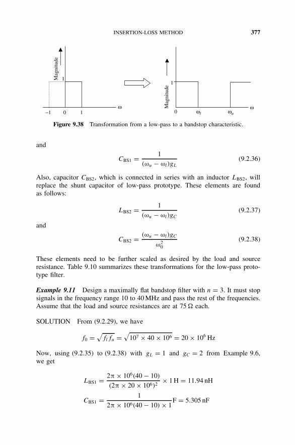
INSERTION-LOSS METHOD 377
Mag
nitu
de
Mag
nitu
de
0 0 ωl ωuω
1 −1
1 1
ω
Figure 9.38 Transformation from a low-pass to a bandstop characteristic.
and
CBS1 = 1
(ωu − ωl)gL
(9.2.36)
Also, capacitor CBS2, which is connected in series with an inductor LBS2, willreplace the shunt capacitor of low-pass prototype. These elements are foundas follows:
LBS2 = 1
(ωu − ωl )gC
(9.2.37)
and
CBS2 = (ωu − ωl )gC
ω20
(9.2.38)
These elements need to be further scaled as desired by the load and sourceresistance. Table 9.10 summarizes these transformations for the low-pass proto-type filter.
Example 9.11 Design a maximally flat bandstop filter with n = 3. It must stopsignals in the frequency range 10 to 40 MHz and pass the rest of the frequencies.Assume that the load and source resistances are at 75 each.
SOLUTION From (9.2.29), we have
f0 = √flfu =
√107 × 40 × 106 = 20 × 106 Hz
Now, using (9.2.35) to (9.2.38) with gL = 1 and gC = 2 from Example 9.6,we get
LBS1 = 2π × 106(40 − 10)
(2π × 20 × 106)2× 1 H = 11.94 nH
CBS1 = 1
2π × 106(40 − 10) × 1F = 5.305 nF

378 FILTER DESIGN
TABLE 9.10 Filter Transformations
Filter Circuit Elements
Low-pass
gL gC
High-pass
1ωc gL
1ωc gC
Bandpass
ωu − ωl
ω20gL
gL ωu − ωl
ωu − ωl
ω20gC
gC
ωu − ωl
Bandstop
1ωu − ωl gL
ω20
ωu − ωl gL 1ωu − ωl gC
ω20
ωu − ωl gC
LBS2 = 1
2π × 106(40 − 10) × 2H = 2.653 nH
and
CBS2 = 2π × 106(40 − 10)
(2π × 20 × 106)2× 2 F = 23.87 nF
Values of required elements are determined next following the load and sourceresistance scaling. Hence,
C1 = C3 = 5.305
75nF = 70.73 pF

INSERTION-LOSS METHOD 379
70.73 pF 70.73 pF
318.3 pF
0.8955 µH 0.8955 µH
0.2 µH
75 Ω
75 Ω
L1
C1C2
L2
C3
L3
Figure 9.39 Bandstop circuit for Example 9.11.
−150
−100
−50
0
50
100
Frequency (rad/s)
−8
−7.5
−7
−6.5
−6
Mag
nitu
de (
dB)
Phas
e (d
eg)
0.1 1 10 100 1000
0.1 1 10 100 1000
0.1 1 10 100 1000
Frequency (rad/s)0.1 1 10 100 1000
Figure 9.40 Characteristics of the bandstop filter shown in Figure 9.39.

380 FILTER DESIGN
L1 = L3 = 75 × 11.94 nH = 0.8955 µH
L2 = 75 × 2.653 nH = 0.1989 µH ≈ 0.2 µH
and
C2 = 23.87
75nF = 318.3 pF
The resulting filter circuit is shown in Figure 9.39. Its frequency response depictedin Figure 9.40 indicates that we have transformed the low-pass prototype to abandstop filter for the 10- to 40-MHz frequency band. As before, the sourceresistance is considered a part of the filter circuit, and therefore its passbandshows a 6-dB insertion loss.
9.3 MICROWAVE FILTERS
The filter circuits presented so far in this chapter use lumped elements. How-ever, these may have practical limitations at microwave frequencies. When thesignal wavelength is short, distances between the filter components need to betaken into account. Further, discrete components at such frequencies may ceaseto operate due to associated parasitic elements and need to be approximated withdistributed components. As found in Chapter 3, transmission line stubs can beused in place of lumped elements. However, there may be certain practical prob-lems in implementing the series stubs. This section begins with a technique todesign a low-pass filter with only parallel connected lines of different character-istic impedance values. It is known as the stepped impedance (or high-Z low-Z)filter. Since this technique works mainly for low-pass filters, the procedure totransform series reactance to shunt that utilizes Kuroda’s identities is summa-rized next. Redundant sections of the transmission line are used to separate filterelements, and therefore this procedure is known as redundant filter synthesis.Nonredundant circuit synthesis makes use of these sections to improve the filterresponse as well. Other methods of designing microwave filters include coupledtransmission lines and resonant cavities. Impedance transformers, discussed inChapter 7, are essentially bandpass filters with different impedance at the two-ports. Interested readers can find detailed design procedures of all these filters inthe references at the end of this chapter.
Low-Pass Filter Design Using Stepped Impedance Distributed Elements
Consider a lossless transmission line of length d and characteristic impedanceZ0, as shown in Figure 9.41(a). If it is equivalent to the T-network shown inFigure 9.41(b), these two must have the same network parameters. The imped-ance matrix of the transmission line was determined in Example 8.4 as follows:

MICROWAVE FILTERS 381
(a)
Z0, β
d
(c)
jB 2
jXL
2jXL
(b)
Z11 − Z12 Z11 − Z12
Z12
Figure 9.41 Lossless transmission line (a), equivalent symmetrical T-network (b), and(c) elements of T-networks.
[Z]line = −jZ0 cot βd −j
Z0
sin βd
−jZ0
sin βd−jZ0 cot βd
(9.3.1)
The impedance matrix of the T-network, [Z]T , may be found as
[Z]T =[
Z11 Z12
Z12 Z11
](9.3.2)
Therefore, if this T-network represents the transmission line, we can write
Z11 = −jZ0 cot βd (9.3.3)
and
Z12 = −jZ0
sin βd(9.3.4)
Hence, Z12 is a capacitive reactance. Circuit elements in the series arm of theT-network are found to be inductive reactance. This is found as follows:
Z11 − Z12 = −jZ0cos βd − 1
sin βd= jZ0
sin (βd/2)
cos (βd/2)= jZ0 tan
βd
2(9.3.5)
382 FILTER DESIGN
Therefore, the series element of the T-network is an inductive reactance whileits shunt element is capacitive, provided that βd < π/2. For βd < π/4, (9.3.4)and (9.3.5) give
B ≈ βd
Z0(9.3.6)
and
XL ≈ Z0βd (9.3.7)
Some special cases are as follows:
1. For Z0 very large, (9.3.6) becomes negligible compared with (9.3.7). There-fore, the equivalent T-network (and hence the transmission line) representsan inductor that is given by
L = Z0βd
ω(9.3.8)
2. For Z0 very small, (9.3.6) dominates over (9.3.7). Therefore, the transmis-sion line is effectively representing a shunt capacitance in this case. It isgiven by
C = βd
ωZ0(9.3.9)
Hence, high-impedance sections (Z0 = Zh) of the transmission line can replacethe inductors, and low-impedance sections (Z0 = Zm) can replace the capacitorsof a low-pass filter. In a design, these impedance values must be selected asfar apart as possible and the section lengths are determined to satisfy (9.3.8)and (9.3.9). When combined with the scaling rules, electrical lengths of theinductive and capacitive sections are found as
(βd)L = R0L
Zh
rad (9.3.10)
and
(βd)C = ZmC
R0rad (8.3.11)
where L and C are normalized element values (g values) of the filter and R0 isthe filter impedance.
Example 9.12 Design a three-element maximally flat low-pass filter with itscutoff frequency as 1 GHz. It is to be used between a 50- load and a generatorwith its internal impedance at 50 . Assume that Zh = 150 and Zm = 30 .

MICROWAVE FILTERS 383
50 Ω
50 ΩL1 = 1 L3 = 1
C2 = 2R0 = 1 R4 = 1
Figure 9.42 Maximally flat low-pass filter with normalized elements’ values for Exam-ple 9.12.
19.1° 19.1°
68.75°
Figure 9.43 Maximally flat low-pass filter for Example 9.12.
SOLUTION From (9.2.15) and (9.2.16),
g0 = g4 = 1
g1 = 2 sinπ
6= 1
g2 = 2 sinπ
2= 2
and
g3 = 2 sin5π
6= 1
If we use a circuit arrangement as illustrated in Figure 9.42, element values canbe scaled for the frequency and the impedance. Using the scaling rules, thesevalues are found as follows (see Figure 9.43):
θ1 = θ3 = (βd)L = 1 × 50
150= 0.3333 rad = 19.1
and
θ2 = (βd)C = 30 × 2
50= 1.2 rad = 68.75
Filter Synthesis Using the Redundant Elements
As mentioned earlier, transmission line sections can replace the lumped elementsof a filter circuit. Richard’s transformation provides the tools needed in such a

384 FILTER DESIGN
design. Further, Kuroda’s identities are used to transform series elements to ashunt configuration that facilitates the design.
Richard’s Transformation
Richard proposed that open- and short-circuited lines could be synthesized likelumped elements through the following transformation:
= tan βd = tanωd
vp
(9.3.12)
where vp is the phase velocity of signal propagating on the line. Since the tangentfunction is periodic with a period of 2π, (9.3.12) is a periodic transformation.Substituting in place of ω, the reactance of the inductor L and of the capacitorC may be written as follows:
jXL = jL = jL tan βd (9.3.13)
and
jXC = −j1
C= −j
1
C tan βd= −j
1
Ccot βd (9.3.14)
Comparison of (9.3.13) and (9.3.14) with the special cases considered in Sec-tion 3.2 indicates that the former represents a short-circuited line with its char-acteristic impedance as L, while the latter is an open-circuited with Z0 as 1/C.Filter impedance is assumed to be unity. To obtain the cutoff of a low-pass filterprototype at unity frequency, the following must hold:
= tan βd = 1 → βd = π
4→ d = λ
8(9.3.15)
Note that the transformation holds only at the cutoff frequency ωc (frequencycorresponding to λ), and therefore the filter response will differ from that ofits prototype. Further, the response repeats every 4 ωc. These transformationsare illustrated in Figure 9.44. These stubs are known as the commensurate linesbecause of their equal lengths.
Kuroda’s Identities
As mentioned earlier, Kuroda’s identities facilitate the design of distributed ele-ment filters, providing the means to transform the series stubs into shunt, or viceversa, to separate the stubs physically, and to render the characteristic impedancerealizable. Figure 9.45 illustrates four identities that are useful in such a trans-formation of networks. These networks employ the unit element (U.E.), which isbasically a λ/8-long line at the cutoff frequency ωc, with specified characteristic

MICROWAVE FILTERS 385
Short
Open
Z0 = L
C1
L
C
d
ω-plane Ω-plane
Z0 =
Figure 9.44 Distributed inductor and capacitor obtained from Richard’s transformation.
Z1
U.E.Z2
U.E.n2Z1
1
n2Z2
(a)
(b)
(c)
(d)
Z2
1 U.E.Z1
Z2
1
U.E.Z1
Z1 U.E.Z1
Z1
n2
U.E.Z2
n2
Z2
Z1
U.E.
Z2
n2
Z1
n2
1:n2
1
n2Z2
n2:1
U.E.n2Z1
n2 = 1 +
Figure 9.45 Kuroda’s identities.
impedance. Inductors represent short-circuited stubs and capacitors open-circuitedstubs. Obviously, its equivalent in lumped circuit theory does not exist.
The first identity is proved below. A similar procedure can be used to verifyothers. The circuits associated with the first identity can be redrawn as shown inFigure 9.46. A short-circuited stub of characteristic impedance Z1 replaces the

386 FILTER DESIGN
d
d Open
d
d
Short
Z1
Z2 n2Z1
n2Z2
Figure 9.46 Illustration of Kuroda’s first identity, shown in Figure 9.45.
series inductor that is followed by a unit element transmission line of charac-teristic impedance Z2. Its transformation gives a unit element transmission lineof characteristic impedance n2Z1 and an open-circuited stub of characteristicimpedance n2Z2 in place of a shunt capacitor.
Following Example 8.10, the transmission matrix of a short-circuited seriesstub with input impedance ZS can be found as follows. The impedance ZS ofthe series stub is given as
ZS = jZ1 tan βd = jZ1 (9.3.16)[A B
C D
]S
=[
1 jZ1
0 1
](9.3.17)
Following Example 8.13, the transmission matrix of the unit element is foundto be
[A B
C D
]U.E.
= cos βd jZ2 sin βd
j sin βd
Z2cos βd
= cos βd
1 jZ2 tan βd
j tan βd
Z21
or[A B
C D
]U.E.
= 1√1 + 2
1 jZ2
j
Z21
(9.3.18)
Since these two elements are connected in cascade, the transmission matrix forthe first circuit in Figure 9.46 is found from (9.3.17) and (9.3.18) as follows:
[A B
C D
]a
=[
A B
C D
]S
·[
A B
C D
]U.E.
= 1√1 + 2
1 − 2Z1
Z2j(Z1 + Z2)
j
Z21
(9.3.19)

MICROWAVE FILTERS 387
Now for the second circuit shown in Figure 9.46, the transmission matrix for theunit element is
[A B
C D
]U.E.
= cos βd
1 jn2Z1 tan βd
j tan βd
n2Z11
= 1√
1 + 2
1 jn2Z1
j
n2Z11
(9.3.20)
Since the impedance ZP of the shunt stub is given as
Zp = −jn2Z2 cot βd = −jn2Z2
(9.3.21)
its transmission matrix may be found, by following Example 8.11, as
[A B
C D
]p
= 1 0
j
n2Z21
(9.3.22)
Hence, the transmission matrix of the circuit shown on right-hand side is found as
[A B
C D
]b
=[
A B
C D
]U.E.
·[
A B
C D
]p
= 1√1 + 2
1 − 2Z1
Z2jn2Z1
j
n2
(1
Z1+ 1
Z2
)1
(9.3.23)On substituting for n2, it is easy to show that this matrix is equal to that foundin (9.3.19).
Example 9.13 Design a three-element maximally flat low-pass filter with itscutoff frequency as 1 GHz. It is to be used between a 50- load and a generatorwith its internal impedance at 50 .
SOLUTION A step-by-step procedure to design this filter is as follows:
ž Step 1.As before, g values for the filter are found from (9.2.15) and (9.2.16) as
g0 = g4 = 1
g1 = 2 sinπ
6= 1
g2 = 2 sinπ
2= 2
and
g3 = 2 sin5π
6= 1

388 FILTER DESIGN
50 Ω
50 Ω
L1 = 1
C2 = 2
L3 = 1
R0 = 1 R4 = 1
(a)
(b)
d
L3Z0 = 1
C2Z0 = 0.5
L1Z0 = 1
d
(c)
C2Z0 = 0.5
d
L1Z0 = 1
L3Z0 = 1
d
d d
U.E. U.E.
Z0 = 1Z0 = 1
d = λ/8 at ω = 1 (e)
Z0 = 50 Ω
Z0 = 25 Ω
Z0 = 50 ΩZ0 = 100 Ω Z0 = 100 Ω
Z0 = 100 ΩZ0 = 100 Ω
(d )
U.E. U.E.
d d
d
Z0 = 2Z0 = 2
Z0 = 2 Z0 = 2
Z0 = 0.5
Figure 9.47 Maximally flat low-pass filter for Example 9.13.
The circuit is drawn with normalized values as shown in Figure 9.47(a).ž Step 2. Using Richard’s transformation, the filter elements are replaced by
stubs. Hence, short-circuited series stubs replace inductors L1 and L3, whilean open-circuited shunt stub replaces the capacitor C2. This is shown inFigure 9.47(b).
ž Step 3. Since the circuit found in step 2 cannot be fabricated in its presentform, unit elements are added on its two sides. This is shown in Fig-ure 9.47(c).
ž Step 4. Using Kuroda’s identity shown in Figure 9.45(a), series stub andunit element combinations are transformed to an open-circuited shunt stuband the unit element. Since Z1 = Z2 = 1, equivalent capacitance C and thecharacteristic impedance of the corresponding stub are found to be C = 1
2 =0.5 and Z0 = 2. Also, the characteristic impedance of each unit element isfound to be 2. This circuit is illustrated in Figure 9.47(d).
ž Step 5. For impedance and frequency scaling, all normalized characteristicimpedances are now multiplied by 50 , and the stub lengths are selectedas λ/8 at 1 GHz. This is shown in Figure 9.47(e).

PROBLEMS 389
SUGGESTED READING
Bahl, I., and P. Bhartia, Microwave Solid State Circuit Design. New York: Wiley, 1988.
Collin, R. E., Foundations for Microwave Engineering. New York: McGraw-Hill, 1992.
Davis, W. A., Microwave Semiconductor Circuit Design. New York: Van Nostrand Rein-hold, 1984.
Elliott, R. S., An Introduction to Guided Waves and Microwave Circuits. Englewood Cliffs,NJ: Prentice Hall, 1993.
Fusco, V. F., Microwave Circuits. Englewood Cliffs, NJ: Prentice Hall, 1987.
Matthaei, G. L., L. Young, and E. M. T. Jones, Microwave Filters, Impedance-MatchingNetworks, and Coupling Structures. Dedham, MA: Artech House, 1980.
Pozar, D. M., Microwave Engineering. New York: Wiley, 1998.
PROBLEMS
9.1. Design a low-pass composite filter with nominal impedance of 50 . Itmust pass all signals up to 10 MHz. Assume that f∞ = 10.05 MHz. Plotits characteristics in the frequency range 1 to 100 MHz.
9.2. Design a high-pass T-section constant-k filter that has a nominal impedanceof 50 and a cutoff frequency of 10 MHz. Plot its frequency response inthe frequency band 100 kHz to 100 MHz.
9.3. Design an m-derived T-section high-pass filter with a cutoff frequency of10 MHz and nominal impedance of 50 . Assume that f∞ = 9.95 MHz.Plot the response of this filter in the frequency band 100 kHz to 100 MHz.
9.4. Design a high-pass composite filter with a cutoff frequency of 10 MHz andimage impedance of 50 in its passband. Assume that f∞ = 9.95 MHz.Plot its response in the frequency range 100 kHz to 100 MHz.
9.5. It is desired to design a maximally flat low-pass filter with at least 25 dB ofattenuation at ω = 2ωc and −1.5 dB at its band edge. How many elementswill be required for this filter? If a Chebyshev filter is used with 1.5 dB ofripple in its passband, find the number of circuit elements.
9.6. Design a low-pass Butterworth filter with a cutoff frequency of 150 MHzand an insertion loss of 50 dB at 400 MHz. It is to be used between a 75-load and a generator with its internal resistance as 75 .
9.7. Design a low-pass Chebyshev filter that exhibits ripples no more than 2 dBin its passband. The filter must pass all frequencies up to 50 MHz andattenuate the signal at 100 MHz by at least 15 dB. The load and the sourceresistance are of 50 each.
9.8. Reconsider Problem 9.7 to design a low-pass filter that exhibits the Cheby-shev response with a 3-dB ripple in its passband. The filter must have 50
at both its input and output ports.

390 FILTER DESIGN
9.9. Design a high-pass Chebyshev filter with a passband ripple magnitudebelow 3 dB. It must pass all frequencies over 50 MHz. A minimum of15 dB of insertion loss is required at 25 MHz. Assume that the load andsource resistances are of 75 each.
9.10. Design a bandpass Chebyshev filter that exhibits no more than 2 dB ofripple in its passband. It must pass the signals that are in the frequencyband 50 to 80 MHz with zero insertion loss. Assume that the load andsource resistances are of 50 each.
9.11. It is desired to design a maximally flat low-pass filter with at least 40 dB ofattenuation at f = 1.1 GHz and −3 dB at f = 1 GHz. How many elementswill be required for this filter? If a Chebyshev filter is used with 3 dB ofripple in its passband, find the number of circuit elements.
9.12. Design a Butterworth filter with a cutoff frequency of 960 MHz and aninsertion loss of 15 dB at 1.5 GHz. It is to be used between a 50- loadand a generator with its internal resistance as 50 .
9.13. Design a low-pass Chebyshev filter that exhibits ripples of no more than1 dB in its passband. The filter must pass all frequencies up to 960 MHzand attenuate the signal at 1.5 GHz by at least 15 dB. The load and thesource resistance are of 50 each.
9.14. Reconsider Problem 9.13 to design a low-pass filter that exhibits the Cheby-shev response with 2 dB of ripple in its passband. The filter must have 50
at both its input and output ports.
9.15. Design a high-pass Chebyshev filter with a passband ripple magnitudebelow 0.5 dB. It must pass all frequencies over 500 MHz. A minimum of20 dB of insertion loss is required at 200 MHz. Assume that the load andsource resistances are of 50 each.
9.16. Design a bandpass Chebyshev filter that exhibits no more than 0.1 dB ofripple in its passband. It must pass the signals that are in the frequencyband 500 to 800 MHz with almost zero insertion loss and provide at least15 dB of attenuation for signals below 300 MHz. Assume that the load andsource resistances are of 75 each.
9.17. Design a high-pass filter that exhibits no more than 2.5 dB of ripple in itspassband. It must pass all frequencies over 100 MHz. A minimum of 40 dBof insertion loss is required at 25 MHz. Assume that the load and sourceresistances are of 50 each.
9.18. Design a maximally flat bandstop filter with n = 5. It must stop the signalsin the frequency range 50 to 80 MHz and pass the rest of the frequencies.Assume that the load and source resistances are of 50 each.

PROBLEMS 391
9.19. Design a fifth-order low-pass Butterworth filter with a cutoff frequencyof 5 GHz. It is to be used between a 75- load and a generator with aninternal resistance of 75 .
9.20. Design a third-order low-pass Chebyshev filter that exhibits ripples of nomore than 1 dB in its passband. The filter must pass all frequencies up to1 GHz. The load and the source resistance are of 50 each.
9.21. Design a fifth-order high-pass Chebyshev filter with passband ripple mag-nitude below 3 dB. It must pass all frequencies over 5 GHz. Assume thatthe load and source resistances are of 75 each.

10SIGNAL-FLOW GRAPHS ANDTHEIR APPLICATIONS
A signal-flow graph is a graphical means of portraying the relationship among thevariables of a set of linear algebraic equations. S. J. Mason originally introducedit to represent the cause and effect of linear systems. Associated terms are definedin this chapter along with a procedure to draw a signal-flow graph for a givenset of algebraic equations. Further, signal-flow graphs of microwave networksare obtained in terms of their S-parameters and associated reflection coefficients.The manipulation of signal-flow graphs is summarized to find the desired transferfunctions. Finally, the relations for transducer power gain, available power gain,and operating power gain are formulated in this chapter.
Consider a linear network that has N input and output ports. It is describedby a set of linear algebraic equations:
Vi =N∑
j=1
Zij Ij i = 1, 2, . . . , N
This says that the effect Vi at the ith port is a sum of gain times causes atits N ports. Hence, Vi represents the dependent variable (effect), and Ij arethe independent variables (cause). Nodes or junction points of the signal-flowgraph represent these variables. The nodes are connected by line segments calledbranches with an arrow on each directed toward the dependent node. The coef-ficient Zij is the gain of a branch that connects the ith dependent node with the
Radio-Frequency and Microwave Communication Circuits: Analysis and Design, Second Edition,By Devendra K. MisraISBN 0-471-47873-3 Copyright 2004 John Wiley & Sons, Inc.
392

SIGNAL-FLOW GRAPHS AND THEIR APPLICATIONS 393
j th independent node. A signal can be transmitted through a branch only in thedirection of the arrow.
The basic properties of a signal-flow graph can be summarized as follows:
ž A signal-flow graph can be used only when the system is linear.ž A set of algebraic equations must be in the form of effects as functions of
causes before its signal-flow graph can be drawn.ž A node is used to represent each variable. Normally, these are arranged from
left to right, following a succession of inputs (causes) and outputs (effects)of the network.
ž Nodes are connected together by branches with an arrow directed towardthe dependent node.
ž Signals travel along the branches only in the direction of the arrows.ž Signal Ik traveling along a branch that connects nodes Vi and Ik is multiplied
by the branch gain Zik. The dependent node (effect) Vi is equal to the sumof the branch gain times the corresponding independent nodes (causes).
Example 10.1 The output b1 of a system is caused by two inputs a1 and a2 asrepresented by the equation
b1 = S11a1 + S12a2
Find its signal-flow graph.
SOLUTION There are two independent variables and one dependent variablein the equation. Locate these three nodes and connect nodes a1 and a2 with b1,as shown in Figure 10.1. The arrows on two branches are directed toward effectb1. Coefficients of input (cause) are shown as the gain of that branch.
Example 10.2 Output b2 of a system is caused by two inputs a1 and a2 asrepresented by the equation
b2 = S21a1 + S22a2
Find its signal-flow graph.
a1
a2b1
S11
S12
Figure 10.1 Signal-flow graph representation of Example 10.1.

394 SIGNAL-FLOW GRAPHS AND THEIR APPLICATIONS
a1
a2
b2
S21
S22
Figure 10.2 Signal-flow graph representation of Example 10.2.
SOLUTION There are again two independent variables and one dependent vari-able in the equation. Locate these three nodes and connect node a1 with b2 anda2 with b2, as shown in Figure 10.2. The arrows on two branches are directedtoward effect b2. Coefficients of input (cause) are shown as the gain of thatbranch.
Example 10.3 The input–output characteristics of a two-port network are givenby the set of linear algebraic equations
b1 = S11a1 + S12a2
b2 = S21a1 + S22a2
Find its signal-flow graph.
SOLUTION There are two independent variables a1 and a2, and two dependentvariables b1 and b2 in this set of equations. Locate the four nodes and thenconnect nodes a1 and a2 with b1. Similarly, connect a1 and a2 with b2, as shownin Figure 10.3. Arrows on the branches are directed toward effects b1 and b2.The coefficients of each input (cause) are shown as the gain of that branch.
Example 10.4 The following set of linear algebraic equations represents theinput–output relations of a multiport network. Find the corresponding signal-flowgraph.
a2b1
S11
S12
a1 b2
S21
S22
Figure 10.3 Signal-flow graph representation of Example 10.3.

SIGNAL-FLOW GRAPHS AND THEIR APPLICATIONS 395
SOLUTION
X1 = R1 + 1
2 + sX2
X2 = −4X1 + R2 − 7Y1 − 1
s + 4X2
Y1 = s
s2 + 3X2
Y2 = 10X1 − sY1
In the first equation, R1 and X2 represent the causes and X1 is the effect. Hence,the signal-flow graph representing this equation can be drawn as illustrated inFigure 10.4.
Now consider the second equation. X1 is the independent variable in it. Further,X2 appears as cause as well as effect. This means that a branch must start andfinish at the X2 node. Hence, when this equation is combined with the first,the signal-flow graph will look as illustrated in Figure 10.5. Next, we add to itthe signal-flow graph of the third equation. It has Y1 as the effect and X2 asthe cause. It is depicted in Figure 10.6. Finally, the last equation has Y2 as adependent variable, and X1 and Y1 are two independent variables. A completesignal-flow graph representation is obtained after superimposing it as shown inFigure 10.7.
R1 X2X1
1
12 + s
Figure 10.4 Signal-flow graph representation of the first equation of Example 10.4.
R1
R2
X1X2
1
−4
Y1
−7
1
−1s + 4
12 + s
Figure 10.5 Signal-flow graph representation of the first two equations of Example 10.4.

396 SIGNAL-FLOW GRAPHS AND THEIR APPLICATIONS
R2
R1 Y1X1 X2
1
−4
−7
1
−1s + 4
12 + s
s
s2 + 3
Figure 10.6 Signal-flow graph representation of the first three equations of Example 10.4.
R1X2
X1
1
−4
Y1
−7
R21
Y2
10
−s
−1s + 4
12 + s
s
s2 + 3
Figure 10.7 Complete signal-flow graph representation of Example 10.4.
10.1 DEFINITIONS AND MANIPULATIONOF SIGNAL-FLOW GRAPHS
Before we proceed with manipulation of signal-flow graphs, it will be useful todefine a few remaining terms.
Input and Output Nodes A node that has only outgoing branches is defined asan input node or source. Similarly, an output node or sink has only incomingbranches. For example, R1, R2, and Y1 are the input nodes in the signal-flowgraph shown in Figure 10.8. This corresponds to the first two equations ofExample 10.4. There is no output node (exclude the dotted branches) in it becauseX1 and X2 have both outgoing as well as incoming branches. Nodes X1 and X2
in Figure 10.8 can be made the output nodes by adding an outgoing branch of

DEFINITIONS AND MANIPULATION OF SIGNAL-FLOW GRAPHS 397
R1
R2
1
−4
Y1
−7
1
X1
X1 X2
X2
1 1
−1s + 4
12 + s
Figure 10.8 Signal-flow graph with R1, R2, and Y1 as input nodes.
unity gain to each node. This is illustrated in Figure 10.8 by dotted branches. Itis equivalent to adding X1 = X1 and X2 = X2 in the original set of equations.Thus, any nonoutput node can be made an output node in this way. However,this procedure cannot be used to convert these nodes to input nodes because thatchanges the equations. If an incoming branch of unity gain is added to node X1,the corresponding equation is modified as follows:
X1 = X1 + R1 + 1
2 + sX2
However, X1 can be made an input node by rearranging it as follows. Thecorresponding signal-flow graph is illustrated in Figure 10.9. It may be notedthat R1 is now an output node:
R1 = X1 − 1
2 + sX2
R1
X2
1
−4
Y1
−7
R21
X1
−1s + 4
12 + s
−
Figure 10.9 Signal-flow graph with R1 as an output, and X1, R2, and Y1 as the inputnodes.

398 SIGNAL-FLOW GRAPHS AND THEIR APPLICATIONS
Path A continuous succession of branches traversed in the same direction iscalled the path. It is known as a forward path if it starts at an input node andends at an output node without hitting a node more than once. The product ofbranch gains along a path is defined as the path gain. For example, there are twoforward paths between nodes X1 and R1 in Figure 10.9. One of these forwardpaths is just one branch connecting the two nodes with a path gain of 1. Theother forward path is X1 to X2 to R1. Its path gain is 4/(2 + s).
Loop A loop is a path that originates and ends at the same node without encoun-tering other nodes more than once along its traverse. When a branch originatesand terminates at the same node, it is called a self-loop. The path gain of a loopis defined as the loop gain.
Once the signal-flow graph is drawn, the ratio of an output to an input node(while other inputs, if there are more than one, are assumed to be zero) can beobtained by using rules of reduction. Alternatively, Mason’s rule may be used.However, the latter rule is prone to error if the signal-flow graph is too complex.The reduction rules are generally recommended for such cases and are givenas follows:
Rule 1 When there is only one incoming and one outgoing branch at a node (i.e.,two branches are connected in series), it can be replaced by a direct branch withbranch gain equal to the product of the two. This is illustrated in Figure 10.10.
Rule 2 Two or more parallel paths connecting two nodes can be merged into asingle path with a gain that is equal to the sum of the original path gains, asdepicted in Figure 10.11.
Rule 3 A self-loop of gain G at a node can be eliminated by multiplying its inputbranches by 1/(1 − G). This is shown graphically in Figure 10.12.
Rule 4 A node that has one output and two or more input branches can be splitin such a way that each node has just one input and one output branch, as shownin Figure 10.13.
R1
X2X2X1 X1
5s 2 10s
Figure 10.10 Graphical illustration of rule 1.
X1 X1X2 X2
5s
5s + 3
3
Figure 10.11 Graphical illustration of rule 2.

DEFINITIONS AND MANIPULATION OF SIGNAL-FLOW GRAPHS 399
X1X1X2 X2
4
2s 41 − 2s
Figure 10.12 Graphical illustration of rule 3.
X1
X2
X5X4
X3
C1
C3
C4
C2
X1
X2
X5
X′′
X′′′
X′4
X3
C1
C3C4
C4
C4
C2
4
4
Figure 10.13 Graphical illustration of rule 4.
X1X4
X3
X5
X2
C1
C4
C3
C2
X1 X5X′′
X′4
X′′′X3
X2
C1
C1
C1
C4
C3
C2
4
4
Figure 10.14 Graphical illustration of rule 5.
Rule 5 This is similar to rule 4. A node that has one input and two or moreoutput branches can be split in such a way that each node has just one input andone output branch. This is shown in Figure 10.14.
Mason’s Gain Rule Ratio T of the effect (output) to that of the cause (input)can be found using Mason’s rule as follows:
T (s) = P11 + P22 + P33 + · · ·
(10.1.1)
where, Pi is the gain of the ith forward path,
= 1 −∑
L(1) +∑
L(2) −∑
L(3) + · · · (10.1.2)
1 = 1 −∑
L(1)(1) +∑
L(2)(1) −∑
L(3)(1) + · · · (10.1.3)

400 SIGNAL-FLOW GRAPHS AND THEIR APPLICATIONS
2 = 1 −∑
L(1)(2) +∑
L(2)(2) −∑
L(3)(2) + · · · (10.1.4)
3 = 1 −∑
L(1)(3) + · · · (10.1.5)
...
L(1) stands for the sum of all first-order loop gains, L(2) is the sum of allsecond-order loop gains, and so on. L(1)(1) denotes the sum of those first-orderloop gains that do not touch path P1 at any node, L(2)(1) denotes the sum of thosesecond-order loop gains that do not touch the path of P1 at any point, L(1)(2)
denotes the sum of those first-order loops that do not touch path P2 at any point,and so on. First-order loop gain was defined earlier. Second-order loop gain is theproduct of two first-order loops that do not touch at any point. Similarly, third-orderloop gain is the product of three first-order loops that do not touch at any point.
Example 10.5 A signal-flow graph of a two-port network is given in Figure 10.15.Using Mason’s rule, find its transfer function Y/R.
SOLUTION There are three forward paths from node R to node Y. Correspond-ing path gains are found as follows:
P1 = 1 × 1 × 1
s + 1× 1
s
s + 2× 3 × 1 = 3s
(s + 1)(s + 2)
P2 = 1 × 6 × 1 = 6
and
P3 = 1 × 1 × 1
s + 1× (−4) × 1 = − 4
s + 1
Next, it has two loops. The loop gains are
L1 = − 3
s + 1
and
L2 = − 5s
s + 2
6
1 1
−3 −5
−4
3 11
1/(s + 1) s/(s + 2)
Y R
Figure 10.15 Signal-flow graph of Example 10.5.
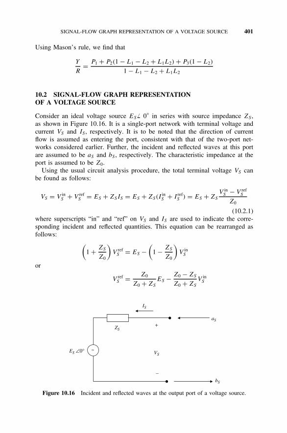
SIGNAL-FLOW GRAPH REPRESENTATION OF A VOLTAGE SOURCE 401
Using Mason’s rule, we find that
Y
R= P1 + P2(1 − L1 − L2 + L1L2) + P3(1 − L2)
1 − L1 − L2 + L1L2
10.2 SIGNAL-FLOW GRAPH REPRESENTATIONOF A VOLTAGE SOURCE
Consider an ideal voltage source ES 0 in series with source impedance ZS ,
as shown in Figure 10.16. It is a single-port network with terminal voltage andcurrent VS and IS , respectively. It is to be noted that the direction of currentflow is assumed as entering the port, consistent with that of the two-port net-works considered earlier. Further, the incident and reflected waves at this portare assumed to be aS and bS , respectively. The characteristic impedance at theport is assumed to be Z0.
Using the usual circuit analysis procedure, the total terminal voltage VS canbe found as follows:
VS = V inS + V ref
S = ES + ZSIS = ES + ZS(IinS + I ref
S ) = ES + ZS
V inS − V ref
S
Z0
(10.2.1)where superscripts “in” and “ref” on VS and IS are used to indicate the corre-sponding incident and reflected quantities. This equation can be rearranged asfollows: (
1 + ZS
Z0
)V ref
S = ES −(
1 − ZS
Z0
)V in
S
or
V refS = Z0
Z0 + ZS
ES − Z0 − ZS
Z0 + ZS
V inS
ES ∠0°
ZS
IS
aS
bS
+
VS
−
~
Figure 10.16 Incident and reflected waves at the output port of a voltage source.

402 SIGNAL-FLOW GRAPHS AND THEIR APPLICATIONS
ΓS
1 bG
bS
aS
aS
bS
1
1
Figure 10.17 Signal-flow graph representation for a voltage source.
Dividing it by√
2Z0, we find that
V refS√2Z0
= Z0
Z0 + ZS
ES√2Z0
− Z0 − ZS
Z0 + ZS
V inS√
2Z0
Using (8.6.15) and (8.6.16), this can be written as follows:
bS = bG + SaS (10.2.2)
where
bS = V refS√2Z0
(10.2.3)
bG =√
Z0ES√2(Z0 + ZS)
(10.2.4)
aS = V inS√
2Z0(10.2.5)
and
S = ZS − Z0
ZS + Z0(10.2.6)
From (10.2.2), the signal flow graph for a voltage source can be drawn as shownin Figure 10.17.
10.3 SIGNAL-FLOW GRAPH REPRESENTATION OF A PASSIVESINGLE-PORT DEVICE
Consider load impedance ZL as shown in Figure 10.18. It is a single-port devicewith port voltage and current VL and IL, respectively. The incident and reflectedwaves at the port are assumed to be aL and bL, respectively. Further, characteristicimpedance at the port is Z0. Following the usual circuit analysis rules, we find that
VL = V inL + V ref
L = ZLIL = ZL(I inL + I ref
L ) = ZL
V inL − V ref
L
Z0

SIGNAL-FLOW GRAPH REPRESENTATION OF A PASSIVE SINGLE-PORT DEVICE 403
ZL
aL
IL
bL
+
VL
−
Figure 10.18 Passive one-port circuit.
or (1 + ZL
Z0
)V ref
L =(
ZL
Z0− 1
)V in
L (10.3.1)
or
V refL = ZL − Z0
ZL + Z0V in
L = LV inL (10.3.2)
After dividing by√
2Z0, we use (8.6.15) and (8.6.16) to find that
bL = LaL (10.3.3)
where
bL = V refL√2Z0
(10.3.4)
aL = V inL√
2Z0(10.3.5)
and
L = ZL − Z0
ZL + Z0(10.3.6)
A signal-flow graph can be drawn on the basis of (10.3.3), as shown in Figure 10.19.
aL aL
bL
ΓL
bL
1
1
Figure 10.19 Signal-flow graph of a one-port passive device.

404 SIGNAL-FLOW GRAPHS AND THEIR APPLICATIONS
ZLTwo-port network Γin
Figure 10.20 Two-port network with termination.
Example 10.6 Impedance ZL terminates port 2 (the output) of a two-port net-work as shown in Figure 10.20. Draw the signal-flow graph and determine thereflection coefficient at its input port using Mason’s rule.
SOLUTION As shown in Figure 10.21, combining the signal-flow graphs of apassive load and that of a two-port network obtained in Example 10.3, we canget the representation for this network. Its input reflection coefficient is given bythe ratio of b1 to a1. For Mason’s rule we find that there are two forward paths,a1 → b1 and a1 → b2 → aL → bL → a2 → b1. There is one loop, b2 → aL →bL → a2 → b2, which does not touch the former path. The corresponding pathand loop gains are
P1 = S11
P2 = S21 × 1 × L × 1 × S12 = LS21S12
and
L1 = 1 × L × 1 × S22 = LS22
Hence,
in = b1
a1= P1(1 − L1) + P2
1 − L1= S11(1 − LS22) + LS21S12
1 − LS22
= S11 + LS21S12
1 − LS22
a1 b2 1S21
b1 a2 1S12
aL
bL
ΓLS11 S22
Load Two-port network
Figure 10.21 Signal-flow graph representation of the network shown in Figure 10.20.

SIGNAL-FLOW GRAPH REPRESENTATION OF A PASSIVE SINGLE-PORT DEVICE 405
ZL
Γout
Two-port network
ZS
VS ∠0° ~
Figure 10.22 Two-port network with the source and termination.
Example 10.7 A voltage source is connected at the input port of a two-port net-work and the load impedance ZL terminates its output, as shown in Figure 10.22.Draw its signal-flow graph and find the output reflection coefficient out.
SOLUTION A signal-flow graph of this circuit can be drawn by combining theresults of Example 10.6 with those of a voltage source representation obtainedin Section 10.2. This is illustrated in Figure 10.23. The output reflection coeffi-cient is defined as the ratio of b2 to a2 with load disconnected, and the sourceimpedance ZS terminates port 1 (the input). Hence, there are two forward pathsfrom a2 to b2, a2 → b2, and a2 → b1 → aS → bS → a1 → b2. There is only oneloop (because the load is disconnected), b1 → aS → bS → a1 → b1. The pathand loop gains are found as follows:
P1 = S22
P2 = S12 × 1 × S × 1 × S21 = SS12S21
andL1 = 1 × S × 1 × S11 = SS11
Therefore, from Mason’s rule, we have
out = b2
a2= P1(1 − L1) + P2
1 − L1= S22(1 − S11S) + S21S12S
1 − S11S
= S22 + S21S12S
1 − S11S
1 1 1 bG
ΓS ΓL
bS aL
bL
a1 b2S21
1 1 aS b1 a2S12
S11 S22
Load Voltage source Two-port network
Figure 10.23 Signal-flow graph representation of the network shown in Figure 10.22.

406 SIGNAL-FLOW GRAPHS AND THEIR APPLICATIONS
ΓS ΓL
1 bG
bS aL
aS
Voltage source Load
bL
1
1
Figure 10.24 Signal-flow graph for Example 10.8.
Example 10.8 The signal-flow graph shown in Figure 10.24 represents a volt-age source that is terminated by a passive load. Analyze the power transfercharacteristics of this circuit and establish the conditions for maximum powertransfer.
SOLUTION Using the defining equations of ai and bi , we can develop thefollowing relations:
power output of the source = |bS |2power reflected back into the source = |aS |2
Hence, power delivered by the source, Pd , is
Pd = |bS |2 − |aS |2
Similarly, we can write the following relations for power at the load:
power incident on the load = |aL|2power reflected from the load = |bL|2 = |L|2|aL|2
where L is the load reflection coefficient. Hence, power absorbed by the load,PL, is given by
PL = |aL|2 − |bL|2 = |aL|2(1 − |L|2) = |bS |2(1 − |L|2)
Since
bS = bG + SaS = bG + SbL = bG + SLaL = bG + SLbS
we find that
bS = bG
1 − SL

SIGNAL-FLOW GRAPH REPRESENTATION OF A PASSIVE SINGLE-PORT DEVICE 407
and
aS = 1
S
(bS − bG) = 1
S
(bG
1 − SL
− bG
)= LbG
1 − SL
Hence,
Pd = |bS |2 − |aS |2 =∣∣∣∣ bG
1 − SL
∣∣∣∣2
−∣∣∣∣ LbG
1 − SL
∣∣∣∣2
=∣∣∣∣ bG
1 − SL
∣∣∣∣2
(1 − |L|2) = |bS |2(1 − |L|2) = PL
This simply says that the power delivered by the source is equal to the powerabsorbed by the load. We can use this equation to establish the load conditionunder which the source delivers maximum power. For that, we consider ways tomaximize.
PL =∣∣∣∣ bG
1 − SL
∣∣∣∣2
(1 − |L|2)
For PL to be a maximum, its denominator 1 − SL is minimized. Let us analyzethis term more carefully using the graphical method. It says that there is a phasorSL at a distance of unity from the origin that rotates with a change in L
(S is assumed constant), as illustrated in Figure 10.25. Hence, the denominatorhas an extreme value whenever SL is a pure real number. If this number ispositive real, the denominator is minimum. On the other hand, the denominatoris maximized when SL is a negative real number.
For SL to be a positive real number, the load reflection coefficient L mustbe the complex conjugate of the source reflection coefficient S . In other words,
L = ∗S ⇒ ZL − Z0
ZL + Z0=
(ZS − Z0
ZS + Z0
)∗
1
1 − ΓSΓL
ΓSΓL
Figure 10.25 Graphical representation of (1 − SL).
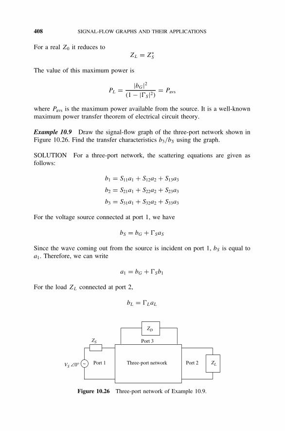
408 SIGNAL-FLOW GRAPHS AND THEIR APPLICATIONS
For a real Z0 it reduces toZL = Z∗
S
The value of this maximum power is
PL = |bG|2(1 − |S |2) = Pavs
where Pavs is the maximum power available from the source. It is a well-knownmaximum power transfer theorem of electrical circuit theory.
Example 10.9 Draw the signal-flow graph of the three-port network shown inFigure 10.26. Find the transfer characteristics b3/bS using the graph.
SOLUTION For a three-port network, the scattering equations are given asfollows:
b1 = S11a1 + S12a2 + S13a3
b2 = S21a1 + S22a2 + S23a3
b3 = S31a1 + S32a2 + S33a3
For the voltage source connected at port 1, we have
bS = bG + SaS
Since the wave coming out from the source is incident on port 1, bS is equal toa1. Therefore, we can write
a1 = bG + Sb1
For the load ZL connected at port 2,
bL = LaL
ZLThree-port network
ZS
ZD
Port 1~ Port 2
Port 3
VS ∠0°
Figure 10.26 Three-port network of Example 10.9.
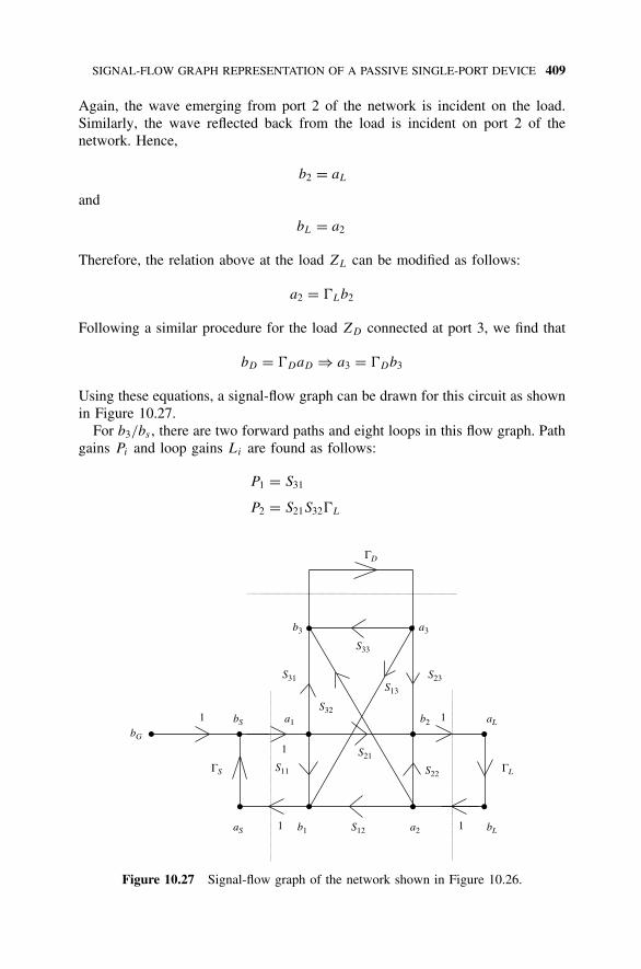
SIGNAL-FLOW GRAPH REPRESENTATION OF A PASSIVE SINGLE-PORT DEVICE 409
Again, the wave emerging from port 2 of the network is incident on the load.Similarly, the wave reflected back from the load is incident on port 2 of thenetwork. Hence,
b2 = aL
and
bL = a2
Therefore, the relation above at the load ZL can be modified as follows:
a2 = Lb2
Following a similar procedure for the load ZD connected at port 3, we find that
bD = DaD ⇒ a3 = Db3
Using these equations, a signal-flow graph can be drawn for this circuit as shownin Figure 10.27.
For b3/bs , there are two forward paths and eight loops in this flow graph. Pathgains Pi and loop gains Li are found as follows:
P1 = S31
P2 = S21S32L
bS
ΓS ΓL
aLa1 b2 1
bG
b3
S33
S31
S11
S21
S22
S32
S23S13
a3
1
1
aS bLb1 S12 a2 11
ΓD
Figure 10.27 Signal-flow graph of the network shown in Figure 10.26.

410 SIGNAL-FLOW GRAPHS AND THEIR APPLICATIONS
L1 = S11S
L2 = S22L
L3 = S33D
L4 = S21S12LS
L5 = S31S23S12DLS
L6 = S13S21S32DLS
L7 = S23S32DL
and
L8 = S13S31DS
Therefore, various terms of Mason’s rule can be evaluated as follows:
1 = 1 − S22L
2 = 1
L(1) = L1 + L2 + L3 + L4 + L5 + L6 + L7 + L8
L(2) = L1L2 + L1L3 + L2L3 + L3L4 + L1L7 + L2L8
L(3) = L1L2L3
Using Mason’s rule we can find that
b3
bS
= P11 + P22
1 − ∑L(1) + ∑
L(2) − ∑L(3)
Note that this signal-flow graph is too complex, and therefore one can easilymiss a few loops. In cases like this, it is prudent to simplify the signal-flowgraph using the five rules mentioned earlier.
10.4 POWER GAIN EQUATIONS
We have seen in the preceding section that maximum power is transferred whenload reflection coefficient L is the conjugate of the source reflection coefficientS . It can be generalized for any port of the network. In the case of an amplifier,maximum power will be applied to its input port if its input reflection coefficientin is the complex conjugate of the source reflection coefficient S . If this isnot the case, the input will be less than the maximum power available from thesource. Similarly, maximum amplified power will be transferred to the load onlyif load reflection coefficient L is the complex conjugate of output reflectioncoefficient out. Part of the power available at the output of the amplifier will be

POWER GAIN EQUATIONS 411
reflected back if there is a mismatch. Therefore, the power gain of an amplifiercan be defined at least three different ways as follows:
transducer power gain, GT = PL
Pavs= power delivered to the load
power available from the source
operating power gain, GP = PL
Pin= power delivered to the load
power input to the network
and
available power gain, GA = PAVN
Pavs= power available from the network
power available from the source
where Pavs is the power available from the source, Pin the power input to thenetwork, PAVN the power available from the network, and PL the power deliveredto the load. Therefore, the transducer power gain will be equal to that of operatingpower gain if the input reflection coefficient in is the complex conjugate of thesource reflection coefficient S . That is,
Pavs = Pin|in=∗S
Similarly, the available power gain will be equal to the transducer power gain ifthe following condition holds at the output port:
PAVN = PL|L=∗out
In this section we formulate these power gain relations in terms of scatteringparameters and reflection coefficients of the circuit. To facilitate the formulation,we reproduce in Figure 10.28 the signal-flow graph obtained in Example 10.7.
bL
ΓL
aLbS
aS
ΓS
1
bG
a1
a2
b2
b1
S21
S12
S22 S11
Pavs Pin PAVN PL
1
1
1
1
Voltage source Amplifier circuit (two-port)Load
Figure 10.28 Signal-flow graph for an amplifier circuit with voltage source and termi-nating load.

412 SIGNAL-FLOW GRAPHS AND THEIR APPLICATIONS
Transducer Power Gain
To develop the relation for transducer power gain, we first determine the powerdelivered to load PL and the power available from the source Pavs:
PL = |aL|2 − |bL|2 = |aL|2(1 − |L|2) = |b2|2(1 − |L|2) (10.4.1)
We derived an expression for Pavs in Example 10.7. That is rewritten here:
Pavs = |bS |2 − |aS |2 = |bG|21 − |S |2 (10.4.2)
Therefore, the transducer power gain is
GT = |b2|2|bG|2 (1 − |L|2)(1 − |S |2) (10.4.3)
We now need to find an expression for b2/bG. Mason’s rule can be used toformulate it. There is only one forward path in this case. However, there arethree loops. The path gain P1 and loop gains Li are
P1 = S21
L1 = S11S
L2 = S22L
and
L3 = S12S21SL
Therefore,
b2
bG
= P1
1 − (L1 + L2 + L3) + L1L2
= S21
1 − (S11S + S22L + S21LS12S) + S11SS22L
(10.4.4)
Substituting (10.4.4) into (10.4.3), we get
GT = |S21|2(1 − |L|2)(1 − |S |2)|1 − (S11S + S22L + S21LS12S) + S11SS22L|2 (10.4.5)
It can be simplified as follows:
GT = |S21|2(1 − |L|2)(1 − |S |2)|(1 − S11S)(1 − S22L) − S21S12LS |2

POWER GAIN EQUATIONS 413
or
GT = |S21|2(1 − |L|2)(1 − |S |2)|(1 − S22L)[1 − S11S − S21S12LS/(1 − S22L)]|2
or
GT = |S21|2(1 − |L|2)(1 − |S |2)|(1 − S22L)(1 − inS)|2
= 1 − |S |2|1 − inS |2 |S21|2 1 − |L|2
|1 − S22L|2 (10.4.6)
where
in = S11 + S21S12L
1 − S22L
(10.4.7)
This is the input reflection coefficient formulated in Example 10.6.Alternatively, (10.4.5) can be written as
GT = |S21|2(1 − |L|2)(1 − |S |2)|(1 − S11S)(1 − outL)|2 = 1 − |S |2
|1 − S11S |2 |S21|2 1 − |L|2|1 − outL|2
(10.4.8)where
out = S22 + S21S12S
1 − S11S
(10.4.9)
This is the output reflection coefficient formulated in Example 10.7.
Special Case Consider the case when the two-port network is unilateral. Thismeans that there is an output signal at port 2 when a source is connected at port1. However, a source (cause) connected at port 2 does not show its response(effect) at port 1. In terms of scattering parameters of the two-port, S12 is equalto zero in this case, and therefore, the input and output reflection coefficientsin (10.4.7) and (10.4.9) simplify as follows:
in = S11
andout = S22
The transducer power gain GT as given by (10.4.6) or (10.4.8) simplifies to
GT |S12=0 = GT U = 1 − |S |2|1 − S11S |2 |S21|2 1 − |L|2
|1 − S22L|2 = GSG0GL (10.4.10)
where GT U may be called the unilateral transducer power gain, while
GS = 1 − |S |2|1 − S11S |2 (10.4.11)
G0 = |S21|2 (10.4.12)

414 SIGNAL-FLOW GRAPHS AND THEIR APPLICATIONS
and
GL = 1 − |L|2|1 − S22L|2 (10.4.13)
Equation (10.4.10) indicates that maximum GT U is obtained when the input andoutput ports are conjugate matched. Hence,
GT Umax = GSmaxG0GLmax (10.4.14)
where
GSmax = GS |S=S∗11
(10.4.15)
and
GLmax = GL|L=S∗22
(10.4.16)
Operating Power Gain
To find the operating power gain, we require the power delivered to the loadand power input to the circuit. We evaluated the power delivered to the loadin (10.4.1). The power input to the circuit is found as follows:
Pin = |a1|2 − |b1|2 = |a1|2(1 − |in|2)Hence,
GP = PL
Pin= |b2|2(1 − |L|2)
|a1|2(1 − |in|2) (10.4.17)
Now we evaluate b2/a1 using Mason’s rule. With the source disconnected, wefind that there is only one forward path and one loop with gains S21 and S22L,respectively. Hence,
b2
a1= S21
1 − S22L
(10.4.18)
Substituting (10.4.18) into (10.4.17), we find that
GP = 1
1 − |in|2 |S21|2 1 − |L|2|1 − S22L|2 (10.4.19)
Available Power Gain
Expressions for maximum powers available from the network and the source areneeded to determine the available power gain. Maximum power available fromthe network PAVN is delivered to the load if the load reflection coefficient is acomplex conjugate of the output. Using (10.4.1), we find that
PAVN = PL|L=∗out
= |b2|2(1 − |L|2) = |b2|2(1 − |out|2) (10.4.20)

POWER GAIN EQUATIONS 415
The power available from the source is given by (10.4.2). Hence,
GA = PAVN
Pavs= |b2|2
|bG|2 (1 − |out|2)(1 − |S |2) (10.4.21)
Next, using Mason’s rule in the signal-flow graph of Figure 10.28, we find that
b2
bG
= S21
1 − (S11S + S22L + S21LS12S) + S11SS22L
= S21
(1 − S11S)(1 − outL)
andb2
bG
∣∣∣∣L=∗
out
= S21
(1 − S11S)(1 − |out|2) (10.4.22)
Now, substituting (10.4.22) into (10.4.21), we get
GA = 1 − |S |2|1 − S11S |2 |S21|2 1
1 − |out|2 (10.4.23)
Example 10.10 The scattering parameters of a microwave amplifier are found at800 MHz as follows (Z0 = 50 ): S11 = 0.45 150
, S12 = 0.01 − 10, S21 =
2.05 10, and S22 = 0.4 − 150. The source and load impedances are 20 and30 , respectively. Determine the transducer power gain, operating power gain,and available power gain.
SOLUTION First we determine the source reflection coefficient S and the loadreflection coefficient L as follows:
S = ZS − Z0
ZS + Z0= 20 − 50
20 + 50= −30
70= −0.429
and
L = ZL − Z0
ZL + Z0= 30 − 50
30 + 50= −20
80= −0.25
Now the input reflection coefficient in and the output reflection coefficient out
can be calculated from (10.4.7) and (10.4.9), respectively:
in = S11 + S21S12L
1 − S22L
= 0.45 150 + (0.01 − 10)(2.05 10
)(−0.25)
1 − (0.4 − 150)(−0.25)
orin = −0.3953 + j0.2253 = 0.455 150.32
416 SIGNAL-FLOW GRAPHS AND THEIR APPLICATIONS
and
out = S22 + S21S12S
1 − S11S
= 0.4 − 150 + (0.01 − 10)(2.05 10
)(−0.429)
1 − (0.45 150)(−0.429)
orout = −0.3568 − j0.1988 = 0.4084 − 150.87
The transducer power gain GT can now be calculated from (10.4.6) or (10.4.8)as follows:
GT = |S21|2(1 − |L|2)(1 − |S |2)|(1 − S22L)(1 − inS)|2 = |S21|2(1 − |L|2)(1 − |S |2)
|(1 − S11S)(1 − outL)|2Hence,
GT = 1 − (0.429)2
|1 − (0.45 150)(−0.429)|2 (2.05)2 1 − (0.252)
|1 − (0.4084 − 150.87)(−0.25)|2= 5.4872
Similarly, from (10.4.19),
GP = 1
1 − |in|2 |S21|2 1 − |L|2|1 − S22L|2
Therefore,
GP = 1
1 − (0.4552)(2.052)
1 − (0.252)
|1 − (0.4 − 150)(−0.25)|2 = 5.9374
The available power gain is calculated from (10.4.23) as follows:
GA = 1 − |S |2|1 − S11S |2 |S21|2 1
1 − |out|2Hence,
GA = 1 − (0.429)2
|1 − (0.45 150)(−0.429)|2 (2.052)1
1 − (0.4084)2= 5.8552
The three power gains can be expressed in decibels as follows:
GT (dB) = 10 log(5.4872) ≈ 7.4 dB
GP (dB) = 10 log(5.9374) ≈ 7.7 dB
and
GA(dB) = 10 log(5.8552) ≈ 7.7 dB

SUGGESTED READING 417
Example 10.11 The scattering parameters of a microwave amplifier are found at2 GHz as follows (Z0 = 50 ): S11 = 0.97 − 43
, S12 = 0.0, S21 = 3.39 140,and S22 = 0.63 − 32. The source and load reflection coefficients are 0.97 43
and 0.63 32, respectively. Determine the transducer power gain, operatingpower gain, and available power gain.
SOLUTION Since S12 is zero, this amplifier is unilateral. Therefore, its inputand output reflection coefficients from (10.4.7) and (10.4.9) may be found asfollows:
input reflection coefficient in = S11 = 0.97 − 43
output reflection coefficient out = S22 = 0.63 − 32
On comparing the input reflection coefficient with that of the source, we findthat one is the complex conjugate of the other. Hence, the source is matchedwith the input port, and therefore the power available from the source is equalto the power input. Similarly, we find that the load reflection coefficient is theconjugate of the output reflection coefficient. Hence, power delivered to the loadwill be equal to power available from the network at port 2. As may be verifiedfrom (10.4.10), (10.4.19), and (10.4.23), these conditions make all three powergains equal. From (10.4.10),
GT U = 1 − |S |2|1 − S11S |2 |S21|2 1 − |L|2
|1 − S22L|2 = 1 − (0.97)2
|1 − (0.97)2|2 (3.39)2
× 1 − (0.63)2
|1 − (0.63)2|2 = 322.42
From (10.4.19),
GP = 1
1 − |in|2 |S21|2 1 − |L|2|1 − S22L|2 = 1
1 − (0.97)2(3.39)2 1 − (0.63)2
|1 − (0.63)2|2= 322.42
From (10.4.23),
GA = 1 − |S |2|1 − S11S | |S21|2 1
1 − |out|2 = 1 − (0.97)2
|1 − (0.97)2|2 (3.39)2 1
1 − (0.63)2
= 322.42
SUGGESTED READING
Collin, R. E., Foundations for Microwave Engineering. New York: McGraw-Hill, 1992.
Davis, W. A., Microwave Semiconductor Circuit Design. New York: Van Nostrand Rein-hold, 1984.

418 SIGNAL-FLOW GRAPHS AND THEIR APPLICATIONS
Fusco, V. F., Microwave Circuits. Englewood Cliffs, NJ: Prentice Hall, 1987.
Gonzalez, G., Microwave Transistor Amplifiers. Upper Saddle River, NJ: Prentice Hall,1997.
Pozar, D. M., Microwave Engineering. New York: Wiley, 1998.
Wolff, E. A., and R. Kaul, Microwave Engineering and Systems Applications. New York:Wiley, 1988.
PROBLEMS
10.1. Use Mason’s rule to find Y (s)/R(s) for the signal-flow graph shown inFigure P10.1.
1 2
−5
1/S 1/S 1
3
1
−4R(s) Y(s)
Figure P10.1
10.2. Use Mason’s gain rule to find Y5(s)/Y1(s) and Y2(s)/Y1(s) for the systemshown in Figure P10.2.
Y1
Y2 Y3 Y4 Y6
Y5
G1
G4
−H1 −H2
−H3
G2 G3
1 1
Figure P10.2

PROBLEMS 419
10.3. Use Mason’s gain rule to find Y2(s)/R3(s) for the system shown in FigureP10.3.
Y3
Y4
Y1
Y61/S 6 1/S
R2(s)
R1(s)
Y2(s)
R3(s)
−2 −3
−4
1 1
Figure P10.3
10.4. Use Mason’s gain rule to find Y (s)/R(s) for the signal-flow graph shownin Figure P10.4.
1 4
13 2
5 7 6
1
1/(S + 1) 1/(S + 1)
R(s)
Y(s)
Figure P10.4
10.5. Draw the signal-flow graph for the circuit shown in Figure P10.5. UseMason’s gain rule to determine the power ratios P2/P1 and P3/P1.
Port 1
Port 3
Port 2
P1
P3
P2
[S ]
Figure P10.5
[S] = 0 S12 0
S21 0 S23
0 S32 0

420 SIGNAL-FLOW GRAPHS AND THEIR APPLICATIONS
in is the reflection coefficient at port 1, and 2 and 3 are the reflectioncoefficients at ports 2 and 3, respectively.
10.6. A voltage source has an internal impedance of 100 , and an electro-motive force of 3 V. Using Z0 = 50 , find the reflection coefficient andscattering variables a and b for the source.
10.7. A 10-mV voltage source has an internal impedance of 100 + j50 .Assuming that the characteristic impedance Z0 is 50 , find the reflec-tion coefficient and scattering variables a and b for the source. Draw thesignal-flow graph.
10.8. A voltage source of 1 0 V has an internal resistance of 80 . It isconnected to a load of 30 + j40 . Assuming that the characteristicimpedance is 50 , find the scattering variables and draw the signal-flowgraph.
10.9. The scattering parameters of a two-port network are S11 = 0.26 − j0.16,S12 = S21 = 0.42, and S22 = 0.36 − j0.57.
(a) Determine the input reflection coefficient and transducer power lossfor ZS = ZL = Z0.
(b) Do the same for ZS = Z0 and ZL = 3Z0.
10.10. Two two-port networks are connected in cascade. The scatteringparameters of the first two-port network are S11 = 0.28, S12 = S21 = 0.56,and S22 = 0.28 − j0.56. For the second network, S11 = S22 = −j0.54and S12 = S21 = 0.84. Determine the overall scattering and transmissionparameters.
10.11. Draw the flow graph representation for the two cascaded circuits ofProblem 10.10. Using Mason’s rule, determine the following: (a) theinput reflection coefficient when the second network is match-terminatedand (b) the forward transmission coefficient of the overall network.
10.12. A GaAs MESFET has the following S-parameters measured at 8 GHz witha 50- reference: S11 = 0.26 − 55
, S12 = 0.08 80, S21 = 2.14 65,
and S22 = 0.82 − 30. For ZL = 40 + j160 and S = 0.31 − 76.87, determine the operating power gain of the circuit.
10.13. The S-parameters of a certain microwave transistor measured at 3 GHzwith a 50- reference are S11 = 0.406 − 100
, S12 = 0, S21 = 5.0 50,and S22 = 0.9 − 60. Calculate the maximum unilateral power gain.
10.14. (a) Find the value of the source impedance that results in maximum powerdelivered to the load in the circuit shown in Figure P10.14. Evaluatethe maximum power delivered to the load.

PROBLEMS 421
Zs
λ /4
10 V ∠0° Z0 = 50 Ω ZL = 50 + j50 Ω
Figure P10.14
(b) Using the value of Zs from part (a), find the Thevenin equivalentcircuit at the load end and evaluate the power delivered to the load.

11TRANSISTOR AMPLIFIER DESIGN
Amplifiers are among the basic building blocks of an electronic system. Althoughvacuum-tube devices are still used in high-power microwave circuits, transis-tors—silicon bipolar junction devices, GaAs MESFETs, heterojunction bipolartransistors (HBTs), and high-electron mobility transistors (HEMTs)—are com-mon in many radio-frequency and microwave designs. The chapter begins withthe stability considerations for a two-port network and the formulation of rele-vant conditions in terms of its scattering parameters. Expressions for input andoutput stability circles are presented next to facilitate the design of amplifiercircuits. Design procedures for various small-signal single-stage amplifiers arediscussed for unilateral as well as bilateral transistors. Noise figure considera-tions in amplifier design are discussed in the following section. An overviewof broadband amplifiers is included. Small-signal equivalent circuits and biasingmechanisms for various transistors are also summarized in subsequent sections.
11.1 STABILITY CONSIDERATIONS
Consider a two-port network that is terminated by load ZL as shown in Figure 11.1.A voltage source VS with internal impedance ZS is connected at its input port.Reflection coefficients at its input and output ports are in and out, respectively. Thesource reflection coefficient is S and the load reflection coefficient is L. Expres-sions for input and output reflection coefficients were formulated in Examples 10.6and 10.7. For this two-port to be unconditionally stable at a given frequency, the
Radio-Frequency and Microwave Communication Circuits: Analysis and Design, Second Edition,By Devendra K. MisraISBN 0-471-47873-3 Copyright 2004 John Wiley & Sons, Inc.
422

STABILITY CONSIDERATIONS 423
ZL
ΓS
Zin, Γin
ΓLZout, Γout
ZS
VS ∠0° Two-port network ~
Figure 11.1 Two-port network with voltage source at its input and a load terminatingthe output port.
following inequalities must hold:
|S | < 1 (11.1.1)
|L| < 1 (11.1.2)
|in| =∣∣∣∣S11 + S21S12L
1 − S22L
∣∣∣∣ < 1 (11.1.3)
and
|out| =∣∣∣∣S22 + S21S12S
1 − S11S
∣∣∣∣ < 1 (11.1.4)
Condition (11.1.3) can be rearranged as follows:∣∣∣∣S11 + S22S21S12L + (S12S21 − S12S21)
S22(1 − S22L)
∣∣∣∣ < 1
or ∣∣∣∣ 1
S22
( + S21S12
1 − S22L
)∣∣∣∣ < 1 (11.1.5)
where = S11S22 − S12S21 (11.1.6)
Since1 − S22L −→
L = 11 − S22 = 1 − |S22| exp(jθ) = A (11.1.7)
This traces a circle on the complex plane as θ varies from zero to 2π. It isillustrated in Figure 11.2. Further, 1/[1 − |S22| exp(jθ)] represents a circle ofradius r with its center located at d , where
r = 1
2
(1
1 − |S22| − 1
1 + |S22|)
= |S22|1 − |S22|2 (11.1.8)

424 TRANSISTOR AMPLIFIER DESIGN
1
S22
A
θ
Figure 11.2 Graphical representation of (11.1.7).
and
d = 1
2
(1
1 + |S22| + 1
1 − |S22|)
= 1
1 − |S22|2 (11.1.9)
Hence, for |L| ≤ 1 and L = θ, condition (11.1.5) may be written as
∣∣∣∣ 1
|S22|(
+ S21S12
1 + |S22| exp(jθ)
1 − |S22|2)∣∣∣∣ < 1
or1
|S22|∣∣∣∣ + S12S21
1 − |S22|2 + S12S21|S22| exp(jθ)
1 − |S22|2∣∣∣∣ < 1 (11.1.10)
Now, using the Minkowski inequality,
(n∑
k=1
|ak + bk|p)1/p
≤(
n∑k=1
|ak|p)1/p
+(
n∑k=1
|bk|p)1/p
(11.1.11)
we find that (11.1.10) is satisfied if
1
|S22|∣∣∣∣ + S12S21
1 − |S22|2∣∣∣∣ + |S12S21|
1 − |S22|2 < 1
or1
|S22|∣∣∣∣ + S12S21
1 − |S22|2∣∣∣∣ < 1 − |S12S21|
1 − |S22|2 (11.1.12)
Since the left-hand side of (11.1.12) is always a positive number, this inequalitywill be satisfied if the following is true:
1 − |S22|2 − |S12S21| > 0 (11.1.13)

STABILITY CONSIDERATIONS 425
Similarly, stability condition (11.1.4) will be satisfied if
1 − |S11|2 − |S12S21| > 0 (11.1.14)
Adding (11.1.13) and (11.1.14), we get
2 − |S11|2 − |S22|2 − 2|S12S21| > 0
or1 − 1
2 (|S11|2 + |S22|2) > |S12S21| (11.1.15)
From (11.1.6) and (11.1.15), we have
|| < |S11S22| + |S12S21| < |S11S22| + 1 − 12 (|S11|2 + |S22|2)
or|| < 1 − 1
2 (|S11| − |S22|)2 ⇒ || < 1 (11.1.16)
Multiplying (11.1.13) and (11.1.14), we get
(1 − |S22|2 − |S12S21|)(1 − |S11|2 − |S12S21|) > 0
or1 − |S11|2 − |S22|2 − 2|S12S21| + ζ > 0 (11.1.17)
whereζ = |S11|2|S22|2 + |S12S21|2 + |S12S21|(|S11|2 + |S22|2)
From the self-evident identity,
|S12S21|(|S11| − |S22|)2 ≥ 0
it can be proved thatζ ≤ ||2
Therefore, (11.1.17) can be written as:
1 − |S11|2 − |S22|2 − 2|S12S21| + ||2 > 0
or1 − |S11|2 − |S22|2 + ||2 > 2|S12S21|
or1 − |S11|2 − |S22|2 + ||2
2|S12S21| > 1
Therefore,
k = 1 − |S11|2 − |S22|2 + ||22|S12S21| > 1 (11.1.18)

426 TRANSISTOR AMPLIFIER DESIGN
If the S-parameters of a transistor satisfy conditions (11.1.16) and (11.1.18), itis stable for any passive load and generator impedance. In other words, thistransistor is unconditionally stable. On the other hand, it may be conditionallystable (stable for limited values of load or source impedance) if one or bothof these conditions are violated. It means that the transistor can provide stableoperation for a restricted range of S and L. A simple procedure to find thesestable regions is to test inequalities (11.1.3) and (11.1.4) for particular load andsource impedances. An alternative graphical approach is to find the circles ofinstability for load and generator reflection coefficients on a Smith chart. Thelatter approach is presented below.
From the expression of input reflection coefficient (10.4.7), we find that
in = S11 + S21S12L
1 − S22L
⇒ in(1 − S22L) = S11(1 − S22L) + S21S12L
or
in = S11 − L(S11S22 − S12S21 − inS22) ⇒ L = S11 − in
− inS22
or
L = S11 − in
− inS22
S22
S22= 1
S22
S11S22 − inS22 − S12S21 + S12S21
− inS22
or
L = 1
S22
(1 + S12S21
− inS22
)= 1
S22
( + S12S21
1 − in −1S22
)(11.1.19)
As before, 1 − inS22−1 represents a circle on the complex plane. It is centered
at 1 with radius |inS22−1|; the reciprocal of this expression is another circle
with center at
1
2
(1
1 + |−1S22| + 1
1 − |−1S22|)
= 1
1 − |−1S22|2
and radius
1
2
(1
1 − |−1S22| − 1
1 + |−1S22|)
= |−1S22|1 − |−1S22|2
Since |in| < 1, the region of stability will include all points on the Smith chartoutside this circle. From (11.1.19), the center of the load impedance circle, CL, is
CL = 1
S22
( + S12S21
1 − |−1S22|2)
= 1
S22
( + S12S21||2
||2 − |S22|2)
or
CL = 1
S22
(1 + S12S21
∗
||2 − |S22|2)
= 1
S22
||2 − |S22|2 + S12S21∗
||2 − |S22|2
STABILITY CONSIDERATIONS 427
or
CL = 1
S22
∗( + S12S21) − |S22|2||2 − |S22|2 = 1
S22
∗S11S22 − |S22|2||2 − |S22|2
Therefore,
CL = ∗S11 − S∗22
||2 − |S22|2 = (S22 − S∗11)
∗
|S22|2 − ||2 (11.1.20)
Its radius, rL, is given by
rL = 1
|S22|∣∣∣∣S12S21|−1S22|
1 − |−1S22|2∣∣∣∣ =
∣∣∣∣ S12S21
||2 − |S22|2∣∣∣∣ (11.1.21)
As explained following (11.1.19), this circle represents the locus of points overwhich the input reflection coefficient in is equal to unity. On one side of thiscircle, the input reflection coefficient is less than unity (stable region); on itsother side it exceeds 1 (unstable region). When load reflection coefficient L iszero (i.e., a matched termination is used), in is equal to S11. Hence, the centerof the Smith chart (reflection coefficient equal to zero) represents a stable pointif |S11| is less than unity. On the other hand, it represents unstable impedancefor |S11| greater than unity. If L = 0 is located outside the stability circle andis found stable, all outside points are stable. Similarly, if L = 0 is inside thestability circle and is found stable, all enclosed points are stable. If L = 0 isunstable, all points on that side of the stability circle are unstable.
Similarly, the locus of S can be derived from (11.1.4), with its center CS andits radius rS given as
CS = ∗S22 − S∗11
||2 − |S11|2 = (S11 − S∗22)
∗
|S11|2 − ||2 (11.1.22)
and
rS = 1
|S11|∣∣∣∣S12S21|−1S11|
1 − |−1S11|2∣∣∣∣ =
∣∣∣∣ S12S21
||2 − |S11|2∣∣∣∣ (11.1.23)
This circle represents the locus of points over which output reflection coefficientout is equal to unity. On one side of this circle, the output reflection coefficientis less than unity (stable region), whereas on its other side it exceeds 1 (unstableregion). When the source reflection coefficient S is zero, out is equal to S22.Hence, the center of the Smith chart (reflection coefficient equal to zero) repre-sents a stable point if |S22| is less than unity. On the other hand, it represents anunstable impedance point for |S22| greater than unity. If S = 0 is located outsidethe stability circle and is found stable, all outside source-impedance points arestable. Similarly, if S = 0 is inside the stability circle and is found stable, allenclosed points are stable. If S = 0 is unstable, all points on that side of thestability circle are unstable.

428 TRANSISTOR AMPLIFIER DESIGN
Example 11.1 The S-parameters of a properly biased transistor are found at2 GHz as follows (50- reference impedance): S11 = 0.894 −60.6, S12 =0.02 62.4, S21 = 3.122 123.6, and S22 = 0.781 −27.6. Determine its sta-bility and plot the stability circles if the transistor is potentially unstable (seeFigure 11.3).
SOLUTION From (11.1.16) and (11.1.18), we get
|| = |S11S22 − S12S21| = 0.6964
and
k = 1 + ||2 − |S11|2 − |S22|22|S12S21| = 0.6071
Since one of the conditions for stability failed above, this transistor is poten-tially unstable.
1180
170
160
150
140
130120
110 100 90 80 7060
50
4030
2010
0−10
−20−30
−40
−50−60
−70−80−90−100−110−120−130
−140
−150
−160
−170
CL
rL
CS
rS
0
0.2
0.5 2 5
10
Figure 11.3 Input and output stability circles for Example 11.1.
AMPLIFIER DESIGN FOR MAXIMUM GAIN 429
Using (11.1.20) to (11.1.23), we can determine the stability circles as follows.For the output stability circle CL = 1.36 46.7 and rL = 0.5. Since |S11| is0.894, L = 0 represents a stable load point. Further, this point is located outsidethe stability circle, and therefore all points outside this circle are stable.
For the input stability circle CS = 1.13 68.5 and rS = 0.2. Since |S22| is0.781, S = 0 represents a stable source impedance point. Further, this pointis located outside the stability circle, and therefore all points outside this circleare stable.
For the output stability circle, draw a radial line at 46.7. With the radiusof the Smith chart as unity, locate the center at 1.36 on this line. It can bedone as follows. Measure the radius of the Smith chart using a ruler scale.Supposing that it is d millimeters, the location of the stability circle is then at1.36d millimeters away on this radial line. Similarly, the radius of the stabilitycircle is 0.5d millimeters. The load impedance must lie outside this circle forthe circuit to be stable. Following a similar procedure, the input stability circleis drawn with its radius as 0.2d millimeters and center at 1.13d millimeters onthe radial line at 68.5. To have a stable design, the source impedance must lieoutside this circle.
11.2 AMPLIFIER DESIGN FOR MAXIMUM GAIN
In this section we first consider the design of an amplifier that uses a unilat-eral transistor (S12 = 0) and has maximum possible gain. A design procedureusing a bilateral transistor (S12 = 0) is developed next that requires simultaneousconjugate matching at its two ports.
Unilateral Case
When S12 is zero, the input reflection coefficient in reduces to S11 and theoutput reflection coefficient out simplifies to S22. To obtain maximum gain, thesource and load reflection coefficients must be equal to S∗
11 and S∗22, respectively.
Further, the stability conditions for a unilateral transistor simplify to |S11| < 1and |S22| < 1.
Example 11.2 The S-parameters of a properly biased BJT are found at 1 GHzas follows (with Z0 = 50 ): S11 = 0.60 −155, S22 = 0.48 −20, S12 = 0,and S21 = 6 180. Determine the maximum gain possible with this transistorand design an RF circuit that can provide this gain.
SOLUTION
1. Stability check:
k = 1 − |S11|2 − |S22|2 + ||22|S12S21| = ∞

430 TRANSISTOR AMPLIFIER DESIGN
because S12 = 0 and
|| = |S11S22 − S12S21| = |S11S22| = 0.2909
Since both of the conditions are satisfied, the transistor is unconditionally stable.
2. The maximum possible power gain of the transistor is found as
GTU = 1 − |s |2|1 − S11s |2 |S21|2 1 − |L|2
|1 − S22L|2
and
GT Umax = 1 − |S∗11|2
|1 − |S11|2|2 |S21|2 1 − |S∗22|2
|1 − |S22|2|2
= 1
1 − 0.6062
(62) 1
1 − 0.482= 73.9257
orGTUmax = 10 log10(73.9257) dB = 18.688 dB
3. For the maximum unilateral power gain,
S = S∗11 = 0.606 155 and L = S∗
22 = 0.48 20
The component values are determined from the Smith chart as illustrated inFigure 11.4.
Corresponding to the reflection coefficient’s magnitude 0.606, the VSWR is4.08. Hence, point D in Figure 11.4 represents the source impedance ZS . Sim-ilarly, point B can be identified as the load impedance ZL. Alternatively, thenormalized impedance can be computed from the reflection coefficient. Then,points D and B can be located on the Smith chart. Now, we need to transformthe zero reflection coefficient (normalized impedance of 1) to S (point D) at theinput and to L (point B) at the output. One way to achieve this is to move firston the unity conductance circle from the center of the chart to point C and thenon the constant-resistance circle to reach point D. Thus, it requires a shunt capac-itor and then a series inductor to match at the input. Similarly, we can follow theunity-resistance circle from 1 to point A and then the constant-conductance circleto reach point B. Thus, a capacitor is connected in series with the load and thenan inductor in shunt to match its output side. Actual values of the componentsare determined as follows.
The normalized susceptance at point C is estimated as j1.7. Hence, the shuntcapacitor on the source side must provide a susceptance of 1.7/50 = 0.034 S.

AMPLIFIER DESIGN FOR MAXIMUM GAIN 431
0
1
10
180
170
160
150
140
130120
110100 90 80
7060
50
4030
2010
0−10
−20−30
−40
−50−60
−70−80−90−100−110−120−130
−140
−150
−160
−170
A
B
C
D
0.2
0.5 52
Figure 11.4 Smith chart illustrating the design of Example 11.2.
50 Ω50 Ω
5.411 pF
5.1725 nH
12.434 nH
2.307 pF
~
Figure 11.5 RF circuit designed for Example 11.2.
Since the signal frequency is 1 GHz, this capacitance must be 5.411 pF. Nowthe change in normalized reactance from point C to point D is determinedas j0.2 − (−j0.45) = j0.65. The positive sign indicates that it is an induc-tor of reactance 0.65 × 50 = 32.5 . The corresponding inductance is found as5.1725 nH. Similarly, the normalized reactance at point A is estimated as −j1.38.Hence, the load requires a series capacitor of 2.307 pF. For transforming the sus-ceptance of point A to that of point B, we need an inductance of (−0.16 −0.48)/50 = −0.0128 S. It is found to be a shunt inductor of 12.434 nH. Thiscircuit is illustrated in Figure 11.5.

432 TRANSISTOR AMPLIFIER DESIGN
Bilateral Case (Simultaneous Conjugate Matching)
To obtain the maximum possible gain, a bilateral transistor must be matched atboth of its ports simultaneously, as shown in Figure 11.6. When its output portis properly terminated, the input side of the transistor is matched with the sourcesuch that in = ∗
S . Similarly, the output port of transistor is matched with theload when its input is matched terminated. Mathematically,
in = ∗S
andout = ∗
L
Therefore,
∗S = S11 + S12S21L
1 − S22L
(11.2.1)
and
∗L = S22 + S12S21S
1 − S11S
(11.2.2)
From (11.2.1),
S = S∗11 + S∗
12S∗21
(1/∗L) − S∗
22
(11.2.3)
and from (11.2.2),
∗L = S22 − (S11S22 − S12S21)S
1 − S11S
= S22 − S
1 − S11S
(11.2.4)
Substituting (11.2.4) in (11.2.3), we have
S = S∗11 + S∗
12S∗21
[(1 − S11S)/(S22 − S)] − S∗22
Transistor
Inputmatch-ingnetwork
Outputmatch-ingnetwork
LoadZL
ΓS Γin ΓL
ZS
VS ∠0°
Γout
~
Figure 11.6 Bilateral transistor with input- and output-matching networks.

AMPLIFIER DESIGN FOR MAXIMUM GAIN 433
or
S =S∗11 + S∗
12S∗21(S22 − S)
1 − S11S − |S22|2 + SS∗22
=S∗11 + S∗
12S∗21(S22 − S)
1 − |S22|2 − (S11 − S∗22)S
or
(1 − |S22|2)S − (S11 − S∗22)2
S = S∗11(1 − |S22|2) − S∗
11(S11 − S∗22)S
+ S∗12S
∗21(S22 − S)
or
(S11 − S∗22)2
S + (||2 − |S11|2 + |S22|2 − 1)S + (S∗11 − S22
∗) = 0
This is a quadratic equation in S and its solution can be found as follows:
S =B1 ±
√B2
1 − 4|C1|22C1
= MS (11.2.5)
whereB1 = 1 + |S11|2 − |S22|2 − ||2
andC1 = S11 − S∗
22
Similarly, a quadratic equation for L can be formulated. Solutions to thatequation are found to be
ML =B2 ±
√B2
2 − 4|C2|22C2
(11.2.6)
where
B2 = 1 + |S22|2 − |S11|2 − ||2and
C2 = S22 − S∗11
If |B1/2C1| > 1 and B1 > 0 in equation (11.2.5), the solution with a minus signproduces |MS | < 1 and that with a positive sign produces |MS | > 1. On otherhand, if |B1/2C1| > 1 with B1 < 0 in this equation, the solution with a plus signproduces |MS | < 1 and the solution with a minus sign produces |MS| > 1.Similar considerations apply to equation (11.2.6) as well.
Observation |Bi/2Ci | > 1 implies that |k| > 1.

434 TRANSISTOR AMPLIFIER DESIGN
Proof: ∣∣∣∣ Bi
2Ci
∣∣∣∣ > 1 ⇒∣∣∣∣1 + |S11|2 − |S22|2 − ||2
2(S11 − S∗22)
∣∣∣∣ > 1
or|1 + |S11|2 − |S22|2 − ||2| > 2|(S11 − S∗
22)|
Squaring on both sides of this inequality, we get
|1 + |S11|2 − |S22|2 − ||2|2 > 4|(S11 − S∗22)|2
and
|S11 − S∗22|2 = (S11 − S∗
22)(S∗11 − S22
∗)
= |S12S21|2 + (1 − |S22|2)(|S11|2 − ||2)
Therefore,
|1 + |S11|2 − |S22|2 − ||2|2 > 4|S12S21|2 + 4(1 − |S22|2)(|S11|2 − ||2)
or
|1 + |S11|2 − |S22|2 − ||2|2 − 4(1 − |S22|2)(|S11|2 − ||2) > 4|S12S21|2
or(1 − |S22|2 − |S11|2 + ||2)2 > 4|S12S21|2
or|1 − |S22|2 − |S11|2 + ||2| > 2|S12S21|
Therefore,|1 − |S22|2 − |S11|2 + ||2|
2|S12S21| > 1 ⇒ k > 1
Also, it can be proved that || < 1 implies that B1 > 0 and B2 > 0. Therefore,minus signs must be used in equations (11.2.5) and (11.2.6).
Since
GT max = (1 − |MS|2)|S21|2(1 − |ML|2)|(1 − S11MS)(1 − S22ML) − S12S21MLMS |2
substituting equations (11.2.5), (11.2.6), and k from (11.1.18) gives
GT max = |S21||S12| (k −
√k2 − 1) (11.2.7)

AMPLIFIER DESIGN FOR MAXIMUM GAIN 435
Maximum stable gain is defined as the value of GT max when k = 1. Therefore,
GMSG =∣∣∣∣S21
S12
∣∣∣∣ (11.2.8)
Example 11.3 The S-parameters of a properly biased GaAs FET HFET-1101are measured using a 50- network analyzer at 6 GHz as follows: S11 = 0.614 −167.4, S21 = 2.187 32.4, S12 = 0.046 65, and S22 = 0.716 −83.Design an amplifier using this transistor for a maximum possible gain.
SOLUTION First we need to test for stability using (11.1.16) and (11.1.18).
|| = |S11S22 − S12S21| = 0.3419
and
k = 1 − |S11|2 − |S22|2 + ||22|S12S21| = 1.1296
Since both of the conditions are satisfied, the transistor is unconditionally stable.For the maximum possible gain, we need to use simultaneous conjugate matching.Therefore, the source and load reflection coefficients are determined from (11.2.5)and (11.2.6) as follows:
MS =B1 −
√B2
1 − 4|C1|22C1
= 0.8673 169.76
and
ML =B2 −
√B2
2 − 4|C2|22C2
= 0.9011 84.48
There are many ways to synthesize these circuits. The design of one of thecircuits is discussed here. As illustrated in Figure 11.7, normalized impedancepoints A and C are identified corresponding to MS and ML, respectively. Therespective normalized admittance points B and D are located next. One way totransform the normalized admittance of unity to that of point B is to add a shuntsusceptance (normalized) of about j2.7 at point E. This can be achieved with acapacitor or a stub of 0.194λ, as shown in Figure 11.8. Now, for moving frompoint E to point B, we require a transmission line of about 0.065λ. Similarly, anopen-circuited shunt stub of 0.297λ will transform the unity value to 1 −j3.4 atpoint F, and a transmission line length of 0.093λ will transform it to the desiredvalue at point D.
Note that both of the shunt stubs are asymmetrical about the main line. Asymmetrical stub is preferable. It can be achieved via two shunt-connected stubsof susceptance j1.35 at the input end and of −j1.7 at the output. This circuit

436 TRANSISTOR AMPLIFIER DESIGN
0
0.2
0.5 1 2 5
10
180
170
160
150
140
130120
110 100 90 8070
6050
4030
2010
0−10
−20−30
−40
−50−60
−70−80−90−100−110−120−130
−140
−150
−160
−170
A
B
C
D
E
F
Figure 11.7 Design of input- and output-side matching networks.
50 Ω
50 Ω
0.194λ
0.297λ
0.065λ
0.093λ
O.C.
O.C.
Figure 11.8 RF part of the amplifier circuit for Example 11.3.

AMPLIFIER DESIGN FOR MAXIMUM GAIN 437
50 Ω
50 Ω
0.15λ
0.065λ
0.093λ
O.C.
O.C.
O.C.
O.C.
0.15λ
0.333λ
0.333λ
Figure 11.9 RF part of the amplifier circuit with symmetrical stubs.
is illustrated in Figure 11.9. The value of the gain is evaluated from (11.2.7)as follows:
GT max = |S21||S12| (k −
√k2 − 1) = 28.728 ⇒ 10 log(28.728) = 14.58 dB
Unilateral Figure of Merit In preceding examples we found that the designwith a bilateral transistor is a bit complex compared with a unilateral case. Theprocedure for the bilateral transistor becomes even more cumbersome when thespecified gain is less than its maximum possible value. It can be simplified byassuming that a bilateral transistor is unilateral. The unilateral figure of meritprovides an estimate of the error associated with this assumption. It can beformulated from (10.4.8) and (10.4.10) as follows:
GT
GT U
= |1 − S22L|2|1 − outL|2 =
∣∣∣∣ 1 − S22L
1 − S22L − S12S21SL/(1 − S11S)
∣∣∣∣2
|1 − S22L|2|1 − outL|2 =
∣∣∣∣ 1
1 − S12S21SL/(1 − S22L)(1 − S11S)
∣∣∣∣2
or
GT
GT U
=∣∣∣∣ 1
1 − X
∣∣∣∣2
where
X = S12S21SL
(1 − S22L)(1 − S11S)

438 TRANSISTOR AMPLIFIER DESIGN
Therefore, the bounds of this gain ratio are given by
1
(1 + |X|)2<
GT
GT U
<1
(1 − |X|)2
When S = S∗11 and L = S∗
22, GT U has a maximum value. In this case, themaximum error introduced by using GT U in place of GT ranges as follows:
1
(1 + U)2<
GT
GT U
<1
(1 − U)2(11.2.9)
where
U = |S12||S21||S11||S22|(1 − |S11|2)(1 − |S22|2) (11.2.10)
The parameter U is known as the unilateral figure of merit.
Example 11.4 The scattering parameters of two transistors are as given below.Compare the unilateral figures of merit of the two. For transistor A, S11 =0.45 150, S12 = 0.01 −10, S21 = 2.05 10, and S22 = 0.4 −150. Fortransistor B, S11 = 0.641 −171.3, S12 = 0.057 16.3, S21 = 2.058 28.5,and S22 = 0.572 −95.7.
SOLUTION From (11.2.10) we find that
U = 0.01 × 2.05 × 0.45 × 0.4
(1 − 0.452)(1 − 0.42)= 0.00551 = UA
for transistor A. Similarly, for transistor B,
U = 0.057 × 2.058 × 0.641 × 0.572
(1 − 0.6412)(1 − 0.5722)= 0.1085 = UB
Hence, the error bounds for these two transistors can be determined from (11.2.9)as follows. For transistor A,
0.9891 <GT
GT U
< 1.0055
and for transistor B,
0.8138 <GT
GT U
< 1.2582
Alternatively, these two results can be expressed in decibels as follows.
−0.0476 dB <GT
GT U
< 0.0238 dB

CONSTANT-GAIN CIRCLES 439
and
−0.8948 dB <GT
GT U
< 0.9976 dB
Conclusion: If S12 = 0 can be assumed for a transistor without introducingsignificant error, the design procedure will be much simpler than that in thebilateral case.
11.3 CONSTANT-GAIN CIRCLES
In Section 11.2 we considered the design of amplifiers for maximum possiblegains. Now, let us consider the design procedure for other amplifier circuits. Wesplit it again into two cases, unilateral and bilateral transistors.
Unilateral Case
We consider two different cases regarding unilateral transistors. In one case it isassumed that the transistor is unconditionally stable because |S11| and |S22| areless than unity. In the other case, one or both of these parameters may be greaterthan unity. Thus, it makes || greater than 1. From (10.4.10),
GT U = 1 − |S |2|1 − S11S |2 |S21|2 1 − |L|2
|1 − S22L|2 = GSG0GL
Expressions of GS and GL in this equation are similar in appearance. Therefore,we can express them by the following general form:
Gi = 1 − |i |2|1 − Siii |2
i = S, ii = 11i = L, ii = 22
(11.3.1)
We consider next two different cases of unilateral transistors. In one, the tran-sistor is unconditionally stable, and in the other case it is potentially unstable. Ifthe unilateral transistor is unconditionally stable, |Sii | < 1. Therefore, maximumGi in (11.3.1) will be given as
Gi max = 1
1 − |Sii |2 (11.3.2)
Impedances that produce Gi max(i = S∗ii ) are called optimum terminations.
Therefore,0 ≤ Gi ≤ Gi max
Values of i that produce a constant gain Gi lie in a circle on the Smith chart.These circles are called constant-gain circles.

440 TRANSISTOR AMPLIFIER DESIGN
We define the normalized gain factor gi as follows:
gi = Gi
Gi max= Gi(1 − |Sii |2) (11.3.3)
Hence,0 ≤ gi ≤ 1
From (11.3.1) and (11.3.2), we can write
gi = 1 − |i |2|1 − Siii |2 (1 − |Sii |2) ⇒ gi |1 − Siii |2 = (1 − |i |2)(1 − |Sii |2)
orgi(1 − Siii)(1 − S∗
ii∗i ) = 1 − |Sii |2 − |i |2 + |i |2|Sii |2
orgi(1 − Siii − S∗
ii∗i + |Sii |2|i |2) = 1 − |Sii |2 − |i |2(1 − |Sii |2)
or(gi |Sii |2 + 1 − |Sii |2)|i |2 − gi(Siii + S∗
ii∗i ) = 1 − gi − |Sii |2
or
i∗i − gi
Siii + S∗ii
∗i
1 − (1 − gi)|Sii |2 + g2i |Sii |2
[1 − (1 − gi)|Sii |2]2
= 1 − gi − |Sii |21 − (1 − gi)|Sii |2 + g2
i |Sii|2[1 − (1 − gi)|Sii |2]2
Therefore,
∣∣∣∣i − giS∗ii
1 − (1 − gi)|Sii |2∣∣∣∣2
= (1 − gi − |Sii|2)[1 − (1 − gi)|Sii |2] + |Sii |2g2i
[1 − (1 − gi)|Sii |2]2
(11.3.4)
which is the equation of a circle, with its center di and radius Ri given as follows:
di = giS∗ii
1 − (1 − gi)|Sii |2 (11.3.5)
and
Ri = (1 − |Sii |2)√1 − gi
1 − (1 − gi)|Sii |2 (11.3.6)
Example 11.5 The S-parameters of a MESFET are given in Table 11.1 (Z0 =50 ). Plot the constant-gain circles at 4 GHz for GL = 0 and 1 dB and GS = 2and 3 dB. Using these plots, design an amplifier for a gain of 11 dB. Calculate

CONSTANT-GAIN CIRCLES 441
TABLE 11.1 S -Parameters of a MESFET
f (GHz) S11 S21 S12 S22
3 0.8 −90 2.8 100 0 0.66 −50
4 0.75 −120 2.5 80 0 0.6 −70
5 0.71 −140 2.3 60 0 0.68 −85
and plot its transducer power gain and input return loss in the frequency band 3to 5 GHz.
SOLUTION Since S12 is zero, this transistor is unilateral. Hence,
k = ∞ and || < 1 (because |S11| < 1 and |S22| < 1)
Therefore, it is unconditionally stable. From (10.4.14) to (10.4.16) we have
GS max = 1
1 − |S11|2 = 1
1 − 0.752= 2.28857 = 3.59 dB
GL max = 1
1 − |S22|2 = 1
1 − 0.62= 1.5625 = 1.92 dB
andG0 = |S21|2 = 2.52 = 6.25 = 7.96 dB
Therefore,GT U max = 3.59 + 1.92 + 7.96 = 13.47 dB
Thus, the maximum possible gain is 2.47 dB higher than the desired value of11 dB. Obviously, this transistor can be used for the present design.
The constant-gain circles can be determined from (11.3.5) and (11.3.6). Theseresults are shown in Table 11.2. As illustrated in Figure 11.10, the gain circles aredrawn from these data. Since G0 is found as 8 dB (approximately), the remaining3 dB needs to be obtained through GS and GL. If we select GS as 3 dB, GL mustbe 0 dB. Alternatively, we can use GS and GL as 2 and 1 dB, respectively, toobtain a transducer power gain of 7.96 + 2 + 1 ≈ 11 dB.
Let us select point A on a 2-dB GS circle and design the input-side network.The corresponding admittance is found at point B, and therefore a normalized
TABLE 11.2 Results for Constant-Gain Circles
GS = 3 dB ≈ 2 gS = 0.875 dS = 0.706 120RS = 0.166
GS = 2 dB = 1.58 gS = 0.691 dS = 0.627 120RS = 0.294
GL = 1 dB = 1.26 gL = 0.8064 dL = 0.52 70RL = 0.303
GL = 0 dB = 1 gL = 0.64 dL = 0.44 70RL = 0.44

442 TRANSISTOR AMPLIFIER DESIGN
0
0.2
0.5 1 2 5
10
180
170
160
150
140
130120
110 100 90 8070
6050
4030
2010
0−10
−20−30
−40
−50−60
−70−80−90−100−110−120−130
−140
−150
−160
−170
A
B
C
D
GS = 2 dB
GL = 1 dB
GL = 0 dB
GS = 3 dB
Figure 11.10 Constant-gain circles and the network design for Example 11.4.
capacitive susceptance of j0.62 is needed in parallel with the source admittanceto reach the input VSWR circle. An open-ended 0.09λ-long shunt stub can beused for this. The normalized admittance is now 1 +j0.62. This admittance canbe transformed to that of point B by a 0.183λ-long section of transmission line.Similarly, point C can be used to obtain GL = 1 dB. A normalized reactanceof j0.48 in series with a 50- load can be used to synthesize this impedance.Alternatively, the corresponding admittance point D is identified. Hence, a shuntsusceptance of −j0.35 (an open-circuit stub of 0.431λ), and then a transmissionline length of 0.044λ can provide the desired admittance. This circuit is illustratedin Figure 11.11.
The return loss is found by expressing |in| in decibels. Since
in = S11 + S12S21L
1 − S22L
and S12 = 0, in = S11; therefore, |in (3 GHz)| = 0.8, |in (4 GHz)| = 0.75, and|in (5 GHz) | = 0.71:
return loss at 3 GHz = 20 log10(0.8) = −1.94 dB
return loss at 4 GHz = 20 log10(0.75) = −2.5 dB
return loss at 5 GHz = 20 log10(0.71) = −2.97 dB

CONSTANT-GAIN CIRCLES 443
50 Ω
50 Ω
0.183λ
0.044λ
0.431λ
0.09λ
O.C.
O.C.
Figure 11.11 RF circuit designed for Example 11.4.
The transducer power gain at 4 GHz is 11 dB (because we designed the circuitfor this gain). However, it will be different at other frequencies. We can evaluateit from (10.4.16) as follows:
GT U = 1 − |S |2|1 − S11S |2 |S21|2 1 − |L|2
|1 − S22L|2
Note that S, L, and the S-parameters of the transistor are frequency dependent.Therefore, we need to determine reflection coefficients at other frequencies beforeusing the formula above. For a circuit designed with reactive discrete compo-nents, the new reactances can be evaluated easily. The corresponding reflectioncoefficients can, in turn, be determined using the appropriate formula. However,we used transmission lines in our design. Electrical lengths of these lines willbe different at other frequencies. We can calculate new electrical lengths byreplacing λ as follows:
λ → fnew
fdesignλnew
At 3 GHz, original lengths must be multiplied by 34 = 0.75 to adjust for the
change in frequency. Similarly, it must be multiplied by 54 = 1.25 for 5 GHz.
The new reflection coefficients can be determined using the Smith chart. Theresults are summarized below.
S Calculations:
Lengths at4 GHz
3 GHz:Lengths and S
5 GHz:Lengths and S
0.09 0.068 0.24 158 0.113 0.41 81
0.183 0.137 0.229

444 TRANSISTOR AMPLIFIER DESIGN
L Calculations:
Lengths at4 GHz
3 GHz:Lengths and L
5 GHz:Lengths and L
0.044 0.033 0.72 109 0.055 0.15 −151
0.431 0.323 0.539
Therefore,
GT U(3 GHz) = 1 − 0.242
|1 − (0.24 158)(0.8 −90)|2 × 2.82
× 1 − 0.722
|1 − (0.72 109)(0.66 −50)|2or
GT U(3 GHz) = 5.4117 = 10 log(5.4117) = 7.33 dB
Similarly,
GT U(5 GHz) = 1 − 0.412
|1 − (0.71 −140)(0.41 81)|2 × 2.32
× 1 − 0.152
|1 − (0.58 −85)(0.15 −141)|2or
GT U(5 GHz) = 4.4008
0.7849 × 1.1284= 4.9688 = 6.96 dB
These return-loss and gain characteristics are displayed in Figure 11.12.If a unilateral transistor is potentially unstable, |Sii | > 1. For |Sii | > 1, the real
part of the corresponding impedance will be negative. Further, Gi in (11.3.1) willbe infinite for i = 1/Sii . In other words, the total loop resistance on the inputside (for i = S) or on the output side (for i = L) is zero. This is the characteristicof an oscillator. Hence, this circuit can oscillate. We can still use the same Smithchart to determine the corresponding impedance provided that the magnitude ofreflection coefficient is assumed as 1/|Sii | instead of |Sii |, while its phase angleis the same as that of Sii , and the resistance scale is interpreted as negative. Thereactance scale of the Smith chart is not affected.
It can be shown that the location and radii of constant-gain circles are stillgiven by (11.3.5) and (11.3.6). The centers of these circles are located along aradial line passing through 1/Sii on the Smith chart. To prevent oscillations, i
must be selected such that the loop resistance is a positive number.
Example 11.6 A GaAs FET is biased at Vds = 5 V and Ids = 10 mA. A 50-ANA is used to determine its S-parameters at 1 GHz. These are found as follows:S11 = 2.27 −120, S21 = 4 50, S12 = 0, and S22 = 0.6 −80.
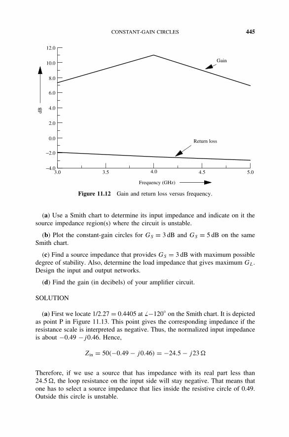
CONSTANT-GAIN CIRCLES 445
Gain
Return loss
−4.0
−2.0
0.0
2.0
4.0
6.0
8.0
10.0
12.0
dB
Frequency (GHz)
3.0 3.5 4.5 5.04.0
Figure 11.12 Gain and return loss versus frequency.
(a) Use a Smith chart to determine its input impedance and indicate on it thesource impedance region(s) where the circuit is unstable.
(b) Plot the constant-gain circles for GS = 3 dB and GS = 5 dB on the sameSmith chart.
(c) Find a source impedance that provides GS = 3 dB with maximum possibledegree of stability. Also, determine the load impedance that gives maximum GL.Design the input and output networks.
(d) Find the gain (in decibels) of your amplifier circuit.
SOLUTION
(a) First we locate 1/2.27 = 0.4405 at −120 on the Smith chart. It is depictedas point P in Figure 11.13. This point gives the corresponding impedance if theresistance scale is interpreted as negative. Thus, the normalized input impedanceis about −0.49 −j0.46. Hence,
Zin = 50(−0.49 − j0.46) = −24.5 − j23
Therefore, if we use a source that has impedance with its real part less than24.5 , the loop resistance on the input side will stay negative. That means thatone has to select a source impedance that lies inside the resistive circle of 0.49.Outside this circle is unstable.

446 TRANSISTOR AMPLIFIER DESIGN
0
0.2
0.5 1 2 5
10
180
170
160
150
140
130120
110 100 90 8070
6050
4030
2010
0−10
−20−30
−40
−50−60
−70−80−90−100−110−120−130
−140
−150
−160
−170
A
B
C
D
P
GS = 5 dB
GS = 3 dB
Figure 11.13 Amplifier design for Example 11.6.
(b) From (11.3.5) and (11.3.6),
dS = gSS∗11
1 − (1 − gS)|S11|2 and RS = (1 − |S11|2)√1 − gS
1 − (1 − gS)|S11|2
where gS = GS(1 − |S11|2); the locations and radii of constant-GS circles arefound as tabulated here:
GS = 5 dB ⇒ 100.5 = 3.1623 GS = 3 dB ⇒ 100.3 = 2
gS = 3.1623(1 − 2.272) = −13.1327 gS = 2(1 − 2.272) = −8.3058
RS = (1 − 2.272)√
1 + 13.1327
1 − (1 + 13.1327)2.272RS = (1 − 2.272)
√1 + 8.3058
1 − (1 + 8.3058)2.272
= 0.2174 = 0.2698
dS = −13.1327(2.27 120)
1 − (1 + 13.1327)2.272dS = −8.3058(2.27 120
)
1 − (1 + 8.3058)2.272
= 0.45 120 = 0.4015 120
These constant-GS circles are shown on the Smith chart in Figure 11.13.

CONSTANT-GAIN CIRCLES 447
50 Ω
50 Ω
0.036λ
0.067λ
0.342λ
0.436 λ
O.C.
O.C.
Figure 11.14 RF circuit for the amplifier of Example 11.6.
(c) To obtain GS = 3 dB with maximum degree of stability, we select point Afor the source impedance because it has a maximum possible real part. Therefore,
ZS ≈ 1 + j0.5 or S = 0.24 76
With ZS = 50 + j25 , the loop resistance in the input side is 50 − 24.5 =25.5 . It is a positive value, and therefore the input circuit will be stable.For maximum GL we select L = S∗
22 = 0.6 80. It is depicted as point Cin Figure 11.13. The corresponding impedance ZL is found to be
ZL = 50(0.55 + j1.03) = 27.5 + j51.5
Now, the input and output circuits can be designed for these values. One suchcircuit is shown in Figure 11.14.
(d) As designed, GS = 3 dB. From (10.4.16),
GL max = 1
1 − |S22|2 = 1
1 − 0.62= 1.5625 = 1.9382 dB
andG0 = |S21|2 = 42 = 16 = 12.0412 dB
Therefore,GT U = 3 + 1.9382 + 12.0412 = 16.9794 dB
Bilateral Case
If a microwave transistor cannot be assumed to be unilateral, the design procedurebecomes tedious for a less than maximum possible transducer power gain. In thiscase, the operating or available power gain approach is preferred because of itssimplicity. The design equations for these circuits are developed in this section.

448 TRANSISTOR AMPLIFIER DESIGN
Unconditionally Stable Case The operating power gain of an amplifier is givenby (10.4.19). For convenience, it is reproduced here:
GP = (1 − |L|2)|S21|2(|1 − S22L|2)(1 − |in|2) (10.4.19)
and the input reflection coefficient is
in = S11 + S12S21L
1 − S22L
= S11 − L
1 − S22L
Therefore,
GP = (1 − |L|2)|S21|2(|1 − S22L|2) − (|S11 − L|2) = |S21|2gp (11.3.7)
where
gp = 1 − |L|2(|1 − S22L|2) − (|S11 − L|2) (11.3.8)
The equation for gp can be simplified and rearranged as follows:
∣∣∣∣L − gpC∗2
1 + gp(|S22|2 − ||2)∣∣∣∣2
= [1 − gp(1 − |S11|2)][1 + gp(|S22|2 − ||2) + g2p|C2|2]
[1 + gp(|S22|2 − ||2)]2(11.3.9)
whereC2 = S22 − S∗
11 (11.3.10)
Equation (11.3.9) can be simplified further as follows:
∣∣∣∣L − gpC∗2
1 + gp(|S22|2 − ||2)∣∣∣∣2
= 1 − 2k|S12S21|gp + |S12S21|2 g2p
[1 + gp(|S22|2 − ||2)]2
This represents a circle with its center cp and radius Rp given as
cp = gpC∗2
1 + gp(|S22|2 − ||2) (11.3.11)
and
Rp =√
(1 − 2k|S12S21|gp + |S12S21|2g2p)
1 + gp(|S22|2 − ||2) (11.3.12)
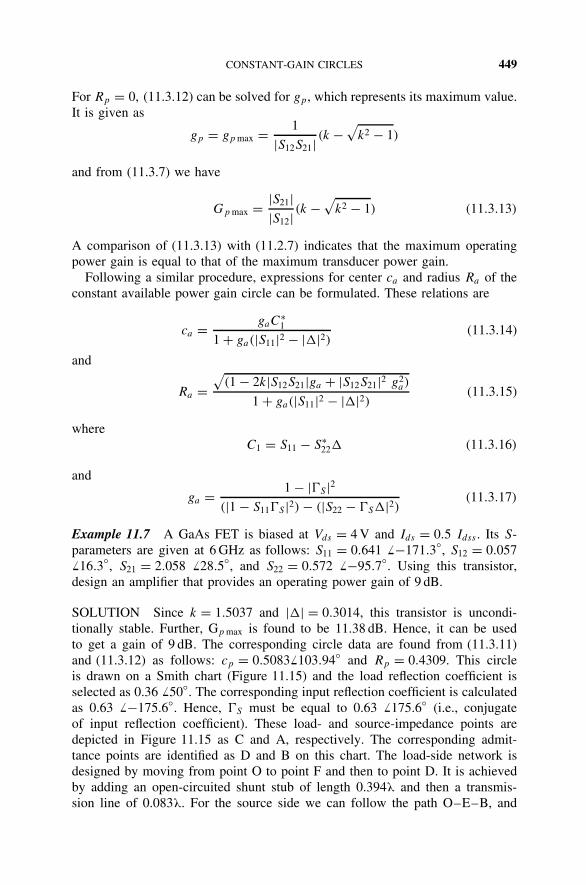
CONSTANT-GAIN CIRCLES 449
For Rp = 0, (11.3.12) can be solved for gp, which represents its maximum value.It is given as
gp = gp max = 1
|S12S21| (k −√
k2 − 1)
and from (11.3.7) we have
Gp max = |S21||S12| (k −
√k2 − 1) (11.3.13)
A comparison of (11.3.13) with (11.2.7) indicates that the maximum operatingpower gain is equal to that of the maximum transducer power gain.
Following a similar procedure, expressions for center ca and radius Ra of theconstant available power gain circle can be formulated. These relations are
ca = gaC∗1
1 + ga(|S11|2 − ||2) (11.3.14)
and
Ra =√
(1 − 2k|S12S21|ga + |S12S21|2 g2a)
1 + ga(|S11|2 − ||2) (11.3.15)
whereC1 = S11 − S∗
22 (11.3.16)
and
ga = 1 − |S |2(|1 − S11S |2) − (|S22 − S|2) (11.3.17)
Example 11.7 A GaAs FET is biased at Vds = 4 V and Ids = 0.5 Idss . Its S-parameters are given at 6 GHz as follows: S11 = 0.641 −171.3, S12 = 0.057 16.3, S21 = 2.058 28.5, and S22 = 0.572 −95.7. Using this transistor,design an amplifier that provides an operating power gain of 9 dB.
SOLUTION Since k = 1.5037 and || = 0.3014, this transistor is uncondi-tionally stable. Further, Gp max is found to be 11.38 dB. Hence, it can be usedto get a gain of 9 dB. The corresponding circle data are found from (11.3.11)and (11.3.12) as follows: cp = 0.5083 103.94 and Rp = 0.4309. This circleis drawn on a Smith chart (Figure 11.15) and the load reflection coefficient isselected as 0.36 50. The corresponding input reflection coefficient is calculatedas 0.63 −175.6. Hence, S must be equal to 0.63 175.6 (i.e., conjugateof input reflection coefficient). These load- and source-impedance points aredepicted in Figure 11.15 as C and A, respectively. The corresponding admit-tance points are identified as D and B on this chart. The load-side network isdesigned by moving from point O to point F and then to point D. It is achievedby adding an open-circuited shunt stub of length 0.394λ and then a transmis-sion line of 0.083λ. For the source side we can follow the path O–E–B, and

450 TRANSISTOR AMPLIFIER DESIGN
0
0.2
0.5 1 2 5
10
180
170
160
150
140
130120
110100 90 80
7060
5040
3020
100
−10−20
−30−40
−50−60
−70−80−90−100−110−120−130
−140
−150
−160
−170
C
D
A
B
E
F
O
Figure 11.15 Matching network design for Example 11.7.
50 Ω
50 Ω
0.076λ
0.083λ
0.394λ
0.161λ
O.C.
O.C.
Figure 11.16 RF circuit of the amplifier for Example 11.6.
therefore an open-circuited shunt stub of 0.161λ followed by a 0.076λ-long trans-mission line can provide the desired admittance. The designed circuit is shownin Figure 11.16.
Potentially Unstable Case Operating power gain circles for a bilateral poten-tially unstable transistor can still be found from (11.3.9) and (11.3.10). However,

CONSTANT-GAIN CIRCLES 451
the load impedance point is selected such that it is in the stable region. Further,the conjugate of its input reflection coefficient must be a stable point because itrepresents the source reflection coefficient. Similarly, the available power gaincircles can be drawn on a Smith chart using (11.3.12) and (11.3.13) along withthe stability circles of the transistor. The source impedance point is selected suchthat it is in the stable region and provides the desired gain. Further, conjugateof the corresponding output reflection coefficient must lie in the stable region aswell because it represents the load.
Example 11.8 A GaAs FET is biased at Ids = 5 mA and Vds = 5 V to measureits scattering parameters at 8 GHz. Using a 50- system, these data are as follows:S11 = 0.5 −180, S12 = 0.08 30, S21 = 2.5 70, and S22 = 0.8 −100.Design an amplifier using this transistor for an operating power gain of 10 dB.
SOLUTION From (11.1.16) and (11.1.18) we find that
|| = 0.2228
andk = 0.3991
Since k is less than 1, this transistor is potentially unstable. The input and outputstability circles are determined from (11.1.20)–(11.1.23) as follows:
For the input stability circle:
CS = 1.6713 170.59
and
rS = 0.9983
Since |S22| is 0.8, S = 0 represents a stable source impedance point. Further,this point is located outside the stability circle, and therefore all points outsidethis circle are stable.
For the output stability circle,
CL = 1.1769 97.17
and
rL = 0.3388
Since |S11| is 0.5, L = 0 represents a stable load impedance point. Further,this point is located outside the stability circle, and therefore, all points outsidethis circle are stable. The data for a 10-dB gain circle are found from (11.3.11)and (11.3.12) as
Cp = 0.5717 97.2 and Rp = 0.4733
These circles are drawn on the Smith chart shown in Figure 11.17. Since thistransistor is potentially unstable for certain load and input impedances, we needto avoid those regions. If we select L = 0.1 97 (point C in Figure 11.17),

452 TRANSISTOR AMPLIFIER DESIGN
0
0.2
0.5 1 2 5
10
180
170
160
150
140
130120
110100 90 80
7060
50
4030
2010
0−10
−20−30
−40
−50−60
−70−80−90−100−110−120−130
−140
−150
−160
−170
D
C
A
B
E
GP = 10 dB
Input stabilitycircle
Output stabilitycircle
Figure 11.17 Design the input- and output-matching networks for Example 11.8.
50 Ω
50 Ω
0.082λ
0.0λ
0.458λ
0.142λ
O.C.
O.C.
Figure 11.18 RF circuit of the amplifier for Example 11.8.
the corresponding input reflection coefficient is calculated as 0.5209 −179.3.Therefore, S is 0.5209 179.3. We find that this point lies in the stable region.One of the possible designs is illustrated in Figure 11.18.
Example 11.9 Design an amplifier for maximum possible transducer powergain, GT max, using a BJT that is biased at VCE = 10 V, IC = 4 mA. Its
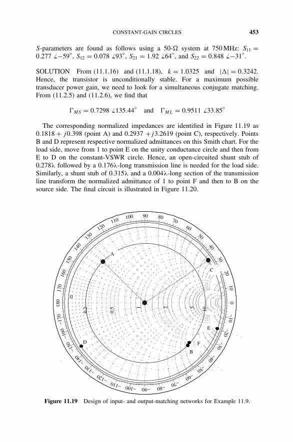
CONSTANT-GAIN CIRCLES 453
S-parameters are found as follows using a 50- system at 750 MHz: S11 =0.277 −59, S12 = 0.078 93, S21 = 1.92 64, and S22 = 0.848 −31.
SOLUTION From (11.1.16) and (11.1.18), k = 1.0325 and || = 0.3242.Hence, the transistor is unconditionally stable. For a maximum possibletransducer power gain, we need to look for a simultaneous conjugate matching.From (11.2.5) and (11.2.6), we find that
MS = 0.7298 135.44 and ML = 0.9511 33.85
The corresponding normalized impedances are identified in Figure 11.19 as0.1818 + j0.398 (point A) and 0.2937 +j3.2619 (point C), respectively. PointsB and D represent respective normalized admittances on this Smith chart. For theload side, move from 1 to point E on the unity conductance circle and then fromE to D on the constant-VSWR circle. Hence, an open-circuited shunt stub of0.278λ followed by a 0.176λ-long transmission line is needed for the load side.Similarly, a shunt stub of 0.315λ and a 0.004λ-long section of the transmissionline transform the normalized admittance of 1 to point F and then to B on thesource side. The final circuit is illustrated in Figure 11.20.
0
0.2
0.5 1 2 5
10
180
170
160
150
140
130120
110 100 90 8070
6050
40
3020
100
−10−20
−30−40
−50−60
−70−80−90−100−110−120
−130
−140
−150
−160
−170
A
C
B
D
E
F
Figure 11.19 Design of input- and output-matching networks for Example 11.9.

454 TRANSISTOR AMPLIFIER DESIGN
50 Ω
50 Ω
0.004λ
0.176λ
0.278λ
0.315λ
O.C.
O.C.
Figure 11.20 RF circuit of the amplifier for Example 11.9.
Example 11.10 Using the BJT of Example 11.9, design an amplifier for Gp =10 dB at 750 MHz. Also, determine the reflection coefficients required to obtainmaximum operating power gain and show that they are identical to those obtainedin Example 11.9 for the simultaneous conjugate match.
SOLUTION From Example 11.9 we know that the transistor is uncondition-ally stable. For an operating power gain of 10 dB, the location and radius ofthe constant-gain circle are determined from (11.3.11) and (11.3.12) as follows:cp = 0.7812 33.85 and Rp = 0.2142. This gain circle is drawn on a Smithchart as shown in Figure 11.21. For an operating power gain of 10 dB, the loadimpedance must be selected on this circle. If we select a normalized impedanceof 1.8 + j1.6 (point C), the load reflection coefficient is 0.56 34. The corre-sponding input reflection coefficient is found at 0.3455 −56.45. Therefore, thesource reflection coefficient S must be equal to 0.3455 56.45. Further, fora maximum operating power gain (i.e., 12.8074 dB), the gain circle convergesto a point that is located at 0.9511 33.85. Hence, this point represents theload reflection coefficient that is needed to obtain maximum operating powergain. Further, the corresponding input reflection coefficient is found to be 0.7298 −135.44. Therefore, S = 0.7298 135.44. A comparison of these resultswith those obtained in Example 11.9 indicates that the results are identical inboth cases.
One of the possible RF circuits for obtaining an operating power gain of10 dB can be designed as follows. After locating the load and source impedancepoints C and A, respectively, constant-VSWR circles are drawn. The correspond-ing normalized admittance points D and B are then found. A normalized shuntsusceptance of −j1.3 will transform the 50- load impedance (normalized admit-tance of 1) to 1 − j1.3 (point E); then a 0.124λ-long transmission line will moveit to point D. An open-circuited 0.356λ-long stub can be used to obtain a −j1.3susceptance.
For the design of an input matching network, a normalized shunt susceptanceof −j0.75 may be used to transform a 50- source impedance (normalized

CONSTANT-GAIN CIRCLES 455
0
0.2
0.5 1 2 5 10
180
170
160
150
140
130120
110 100 90 80 7060
50
40
3020
100
−10−20
−30−40
−50 −60
−70−80−90−100−110−120−130
−140
−150
−160
−170
D
A
B
E
F
GP = 10 dB
C
Figure 11.21 Design of input- and output-matching networks for Example 11.10.
50 Ω
50 Ω
0.075λ
0.124λ
0.356λ
0.397λ
O.C.
O.C.
Figure 11.22 RF circuit of the amplifier for Example 11.10.
admittance of 1) to 1 − j0.75 (point F). A 0.075λ-long transmission line is thenconnected to transform this admittance to that of point B. A 0.397λ-long open-circuited stub can be used to obtain the desired susceptance of −j0.75. The finalcircuit is illustrated in Figure 11.22.
Example 11.11 A suitably biased GaAs FET has the following S-parametersmeasured at 2 GHz with a 50- system: S11 = 0.7 −65, S12 = 0.03 60,
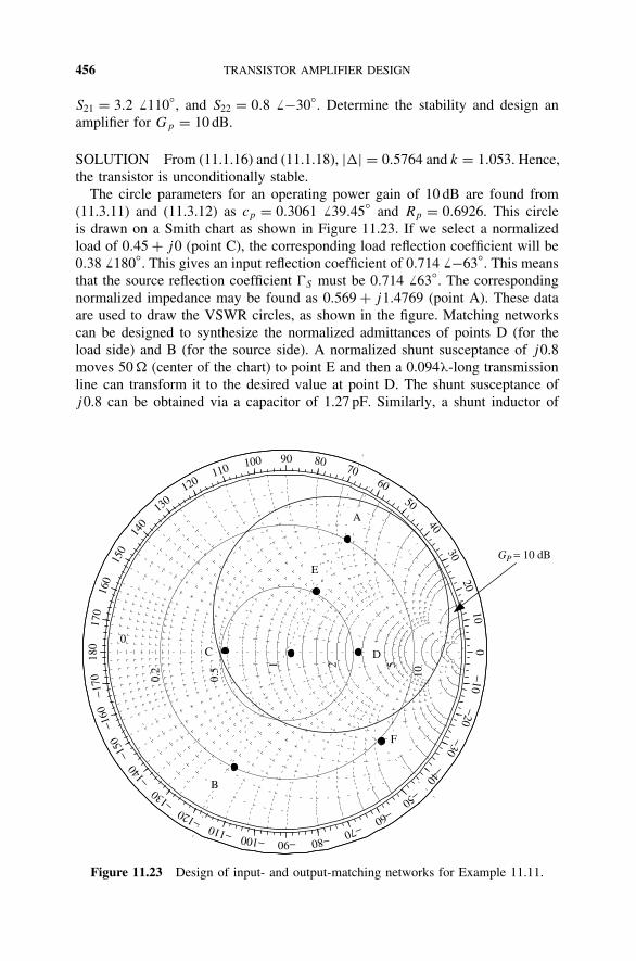
456 TRANSISTOR AMPLIFIER DESIGN
S21 = 3.2 110, and S22 = 0.8 −30. Determine the stability and design anamplifier for Gp = 10 dB.
SOLUTION From (11.1.16) and (11.1.18), || = 0.5764 and k = 1.053. Hence,the transistor is unconditionally stable.
The circle parameters for an operating power gain of 10 dB are found from(11.3.11) and (11.3.12) as cp = 0.3061 39.45 and Rp = 0.6926. This circleis drawn on a Smith chart as shown in Figure 11.23. If we select a normalizedload of 0.45 + j0 (point C), the corresponding load reflection coefficient will be0.38 180. This gives an input reflection coefficient of 0.714 −63. This meansthat the source reflection coefficient S must be 0.714 63. The correspondingnormalized impedance may be found as 0.569 + j1.4769 (point A). These dataare used to draw the VSWR circles, as shown in the figure. Matching networkscan be designed to synthesize the normalized admittances of points D (for theload side) and B (for the source side). A normalized shunt susceptance of j0.8moves 50 (center of the chart) to point E and then a 0.094λ-long transmissionline can transform it to the desired value at point D. The shunt susceptance ofj0.8 can be obtained via a capacitor of 1.27 pF. Similarly, a shunt inductor of
0
0.2
0.5 1 2 5
10
180
170
160
150
140
130120
110 100 90 8070
6050
4030
2010
0−10
−20−30
−40
−50−60
−70−80−90−100−110−120−130
−140
−150
−160
−170
A
C D
B
E
F
GP = 10 dB
Figure 11.23 Design of input- and output-matching networks for Example 11.11.

CONSTANT NOISE FIGURE CIRCLES 457
50 Ω
50 Ω
0.101λ
0.094λ
1.89 nH
1.27 pF
Figure 11.24 Circuit of the amplifier for Example 11.11.
1.89 nH adds a normalized susceptance of −j2.1 at the source side (point F),and then a 0.101λ-long transmission line can transform that to the desired valueof 0.22 − j0.6 (point B). The final circuit is illustrated in Figure 11.24.
11.4 CONSTANT NOISE FIGURE CIRCLES
Noise characteristics of the two-port networks are considered in Chapter 2. Wefound that the noise factor of an amplifier can be expressed via (2.5.21) as follows:
F = Fmin + Rn
GS
|YS − Yopt|2 (11.4.1)
where Fmin = minimum noise factor of the transistor (attained for YS = Yopt)Rn = equivalent noise resistance of the transistorGS = real part of the source admittance
YS = GS + jBS = 1
Z0
1 − S
1 + S
= source admittance presented to the
transistorS = source reflection coefficient seen by the transistor
Yopt = 1
Z0
1 − opt
1 + opt= optimum source admittance that results in
minimum noise figureopt = optimum source reflection coefficient that results in minimum noise
figure
Since
|YS − Yopt|2 =∣∣∣∣ 1
Z0
1 − S
1 + S
− 1
Z0
1 − opt
1 + opt
∣∣∣∣2
= 4
|Z0|2|S − opt|2
|1 + S |2 · |1 + opt|2(11.4.2)

458 TRANSISTOR AMPLIFIER DESIGN
and
GS = Re(YS) = 1
2Z0
(1 − S
1 + S
+ 1 − ∗S
1 + ∗S
)= 1 − |S |2
Z0|1 + S |2 (11.4.3)
(11.4.1) can be written as
F = Fmin + 4Rn
Z0
|S − opt|2(1 − |S |2)|1 + opt|2
or|S − opt|2
1 − |S |2 = F − Fmin
4(Rn/Z0)|1 + opt|2 = N (11.4.4)
where N is called the noise figure parameter.From (11.4.4), we have
|S − opt|2 = N(1 − |S |2)
or
(S − opt)(∗S − ∗
opt) = S∗S − (∗
Sopt + S∗opt) + opt
∗opt = N − N |S |2
or
S∗S − ∗
Sopt + S∗opt
N + 1+ |opt|2
(N + 1)2= N − opt
∗opt
N + 1+ |opt|2
(N + 1)2
or ∣∣∣∣S − opt
N + 1
∣∣∣∣2
= N(N + 1) − N |opt|2(N + 1)2
Hence, ∣∣∣∣S − opt
N + 1
∣∣∣∣ =√
N(N + 1) − N |opt|2N + 1
(11.4.5)
Equation (11.4.5) represents a circle on the complex S-plane. Its center CNF
and radius RNF are given by
CNF = opt
N + 1(11.4.6)
and
RNF =√
N(N + 1) − N |opt|2N + 1
(11.4.7)
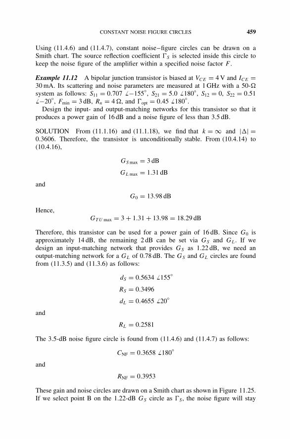
CONSTANT NOISE FIGURE CIRCLES 459
Using (11.4.6) and (11.4.7), constant noise–figure circles can be drawn on aSmith chart. The source reflection coefficient S is selected inside this circle tokeep the noise figure of the amplifier within a specified noise factor F .
Example 11.12 A bipolar junction transistor is biased at VCE = 4 V and ICE =30 mA. Its scattering and noise parameters are measured at 1 GHz with a 50-system as follows: S11 = 0.707 −155, S21 = 5.0 180, S12 = 0, S22 = 0.51 −20, Fmin = 3 dB, Rn = 4 , and opt = 0.45 180.
Design the input- and output-matching networks for this transistor so that itproduces a power gain of 16 dB and a noise figure of less than 3.5 dB.
SOLUTION From (11.1.16) and (11.1.18), we find that k = ∞ and || =0.3606. Therefore, the transistor is unconditionally stable. From (10.4.14) to(10.4.16),
GS max = 3 dB
GL max = 1.31 dB
and
G0 = 13.98 dB
Hence,GT U max = 3 + 1.31 + 13.98 = 18.29 dB
Therefore, this transistor can be used for a power gain of 16 dB. Since G0 isapproximately 14 dB, the remaining 2 dB can be set via GS and GL. If wedesign an input-matching network that provides GS as 1.22 dB, we need anoutput-matching network for a GL of 0.78 dB. The GS and GL circles are foundfrom (11.3.5) and (11.3.6) as follows:
dS = 0.5634 155
RS = 0.3496
dL = 0.4655 20
and
RL = 0.2581
The 3.5-dB noise figure circle is found from (11.4.6) and (11.4.7) as follows:
CNF = 0.3658 180
and
RNF = 0.3953
These gain and noise circles are drawn on a Smith chart as shown in Figure 11.25.If we select point B on the 1.22-dB GS circle as S , the noise figure will stay

460 TRANSISTOR AMPLIFIER DESIGN
0
0.2
0.5 1 2 5
10
180
170
160
150
140
130120
110 100 90 80 7060
50
4030
2010
0−10
−20−30
−40
−50−60
−70−80−90−100−110−120
−130
−140
−150
−160
−170
A
B
C
D
GL = 0.78 dB
GS = 1.22 dB
NF = 3.5 dB
Figure 11.25 Design of input- and output-matching networks for Example 11.12.
within 3.5 dB. The load-side matching network is designed so that it provides GL
as 0.78 dB. We select point D for L. The two matching networks are designedbelow using discrete components.
For the design of a source-side network, we can move on the unity-conductancecircle from 1 to point A. It requires a shunt capacitor for a normalized susceptanceof +j0.75. A capacitor of 2.39 pF can provide this susceptance at 1 GHz. Thenext step is to reach point B from A by moving on the constant-resistance circleof 0.65, which requires an inductive reactance of normalized value +j0.56 andhence an inductor of 4.46 nH. Similarly, the load-side network can be designedfollowing the unity-resistance circle from 1 to point C. It requires a capacitorof 2.27 pF in series with a 50- output. Next, move from point C to D onthe conductance circle of 0.35. Hence, it requires an inductor of 19.89 nH. Thecomplete RF circuit is shown in Figure 11.26.
Example 11.13 A GaAs FET has the following scattering and noise parametersat 4 GHz, measured with a 50- system: S11 = 0.6 − 60, S21 = 1.9 81,S12 = 0.05 26, S22 = 0.5 − 60, Fmin = 1.6 dB, Rn = 20 , and opt = 0.62 100.

CONSTANT NOISE FIGURE CIRCLES 461
50 Ω50 Ω
2.39 pF
4.46 nH
19.89 nH
2.27 pF
~
Figure 11.26 RF circuit design for Example 11.12.
(a) Assuming the FET to be unilateral, design an amplifier for a maximumpossible gain and a noise figure no more than 2.0 dB. Estimate the error introducedin GT due to this assumption.
(b) Redesign the amplifier in part (a), with FET being bilateral.
SOLUTION From (11.1.16) and (11.1.18), || = 0.3713 and k = 2.778. Hence,the transistor is unconditionally stable.
(a) The unilateral figure of merit is found from (11.2.10) as 0.0594. Therefore,
−0.501 dB <GT
GT U
< 0.5938 dB
This means that the maximum error in the gain of the amplifier due to thisassumption will be on the order of ±0.5 dB.
Using (10.4.14) to (10.4.16), we find that
GS max = 1.9382 dB
GL max = 1.25 dB
and
G0 = 5.5751 dB
Therefore,GT U max = 1.9382 + 1.25 + 5.5751 = 8.7627 dB
Since we are looking for a maximum possible gain with a noise figure less than2 dB, we should use load impedance that provides a conjugate match. Note thatthis selection does not influence the noise figure. Thus, we select L = S∗
22 =0.5 60. It is depicted by point C on the Smith chart in Figure 11.27. For thedesign of the source side, we first determine the relevant gain and noise circles.

462 TRANSISTOR AMPLIFIER DESIGN
0
0.2
0.5 1 2 5
10
180
170
160
150
140
130120
110 100 90 80 7060
50
2010
0−10
−20−30
−40
−50−60
−70−80−90−100−110−120−130
−140
−150
−160
−170
A
B
C
D
GS = 1.5 dB
NF = 2 dB
GS = 1.7 dB
30
40
Figure 11.27 Design of input- and output-matching networks for Example 11.13(a).
From (11.3.5) and (11.3.6), the constant-gain circles for GS = 1.5 dB and 1.7dB are determined as follows. For GS = 1.5 dB,
dS = 0.5618 60, RS = 0.2054
For GS = 1.7 dB,dS = 0.5791 60
, RS = 0.1507
The 2-dB noise figure circle is found from (10.4.6) and (10.4.7) as follows:
CNF = 0.5627 100
and
RNF = 0.2454
These circles are drawn on a Smith chart as shown in Figure 11.27. We findthat the 2-dB noise figure circle almost touches the GS = 1.7-dB circle at a point.

CONSTANT NOISE FIGURE CIRCLES 463
50 Ω
50 Ω
0.065λ
0.091λ
0.092λ
0.107λ
sc
sc
Figure 11.28 RF circuit of the amplifier for Example 11.13(a).
Further, the 1.5-dB gain circle has a larger radius. It suggests that a gain largerthan 1.7 dB will have a higher noise figure. As illustrated, the optimum S forthis problem is point A. A circuit designed with short-circuited shunt stubs andtransmission line lengths is shown in Figure 11.28.
(b) When the transistor is bilateral, we need to use the operating power gainor available power gain approach for the design. The operating power gainapproach provides information about the load impedance. Source impedance isdetermined subsequently as a complex conjugate of the input impedance. If thisvalue of the source impedance does not satisfy the noise figure specification,one needs to select a different load impedance. Thus, several iterations may beneeded before the noise and gain requirements are satisfied. On the other hand,the available power gain approach provides the source impedance. The loadimpedance is then determined as a complex conjugate of the output impedance.Hence, a suitable source impedance can be determined that simultaneously satis-fies both the gain and the noise characteristics. Hence, the available power gainapproach does not require iterative calculations, and therefore it is preferable inthe present case.
From (11.3.14) and (11.3.15), the 8-dB gain circle is found as follows: ca =0.5274 64.76 and Ra = 0.2339. Further, the maximum possible available powergain is found to be 8.5 dB. It represents a point at 0.5722 64.76. The noisecircle stays the same as in part (a). These circles are drawn on a Smith chartas shown in Figure 11.29. If we select S as 0.535 90, the noise figure stayswell below 2 dB. The corresponding output reflection coefficient is found to be0.5041 − 67.83. Hence, the load reflection coefficient must be 0.5041 67.83.Now, the input and output matching networks can easily be designed. The trans-ducer power gain of this circuit is found from (10.4.8) to be 8 dB.
A comparison of the gain obtained in part (b) with that in part (a) shows thatthe two differ by 0.76 dB. However, the uncertainty predicted in part (a) is about±0.5 dB. The 8.2-dB gain circle shown in Figure 11.29 indicates that the gain inpart (b) can be increased to a little over 8.2 dB. That will bring the two valueswithin the range predicted.

464 TRANSISTOR AMPLIFIER DESIGN
0
0.2
0.5 1 2 5
10
180
170
160
150
140
130120
110 100 90 8070
6050
4030
2010
0−10
-20−30
−40
−50−60
−70−80−90−100−110−120−130
−140
−150
−160
−170
GA = 8.5 dB
NF = 2 dB
ΓS
GA = 8.2 dB
GA = 8 dB
ΓL
Figure 11.29 Available power gain circles and RF circuit design for Example 11.13(b).
Example 11.14 An Avantek low-noise silicon bipolar transistor, AT-41410,is biased at VCE = 8 V and IC = 10 mA. Its scattering and noise parametersare measured at 1 GHz with a 50- system. The results are found as follows:S11 = 0.6 −163, S21 = 7.12 86, S12 = 0.039 35, S22 = 0.5 −38, Fmin =1.3 dB, Rn = 8 , and opt = 0.06 49. Design the input and output matchingnetworks of an amplifier that provides a power gain of 16 dB with a noise figurebelow 2.5 dB.
SOLUTION From (11.1.16) and (11.1.18), || = 0.1892 and k = 0.7667.Hence, the transistor is potentially unstable. The input stability circle isdetermined from (11.1.22) and (11.1.23) as follows: CS = 1.7456 171.69 andrS = 0.8566. Since |CS | is larger than rS , this circle does not enclose the centerof a Smith chart (S = 0). Further, the output reflection coefficient out is equalto S22 for S = 0. Hence, |out| is 0.5 at this point and provides a stable circuitwith this transistor. Therefore, the stability circle encloses the unstable region(i.e., the inside is unstable).
Similarly, the output stability circle is found from (11.1.20) and (11.1.21)as follows: CL = 2.1608 50.8 and rL = 1.2965. Again, the center of a Smith

CONSTANT NOISE FIGURE CIRCLES 465
chart (L = 0) is outside this circle because |CL| is larger than rL. Since the inputreflection coefficient in is equal to S11 at this point, |in| is 0.6. Hence, it repre-sents the load impedance that will provide a stable operation for this transistor.Therefore, all impedances on a Smith chart that are outside the stability circlerepresent the stable region, and those enclosed by the stability circle are unstable.
Since the transistor is bilateral and we want a noise figure below 2.5 dB,we use the available power gain approach. The 16-dB gain circle is foundfrom (11.3.14) and (11.3.15) as follows: ca = 0.3542 171.69 and Ra = 0.6731.The 2.5-dB noise figure circle is found from (11.4.6) and (11.4.7) as follows:CNF = 0.0346 40 and RNF = 0.6502. These circles are drawn on a Smith chartillustrated in Figure 11.30. If we select S at point B (S = 0.13 0), out isfound to be 0.469 −36.45. Hence, the load reflection coefficient L must beequal to 0.469 36.45 (point D).
For an input-side network, we can move from point E to A on the unity-resistance circle by adding a normalized reactance of about −j0.55 (i.e.,−j27.5 ) in series with 50 . It requires a capacitor of 5.7874 pF at 1 GHz.We then move on the conductance circle of 0.77 to reach point B from A. Itmeans that we need a normalized susceptance of −j0.43 (i.e., −j0.0086 S).Hence, an inductor of 18.5064 nH connected in shunt will suffice.
0
0.2
0.5 1 2 5
10
180
170
160
150
140
130120
110 100 90 80 7060
50
40
3020
100
−10−20
−30−40
−50-60
−70−80−90−100−110−120−130
−140
−150
−160
−170
A
B
C
D
Output stability circle(unstable region)
Input stability circle(unstable region)
N F = 2.5 dB
GA = 16 dB
=
ΓS
ΓL
E
Figure 11.30 Design of input- and output-matching networks for Example 11.14.

466 TRANSISTOR AMPLIFIER DESIGN
50 Ω
50 Ω
5.79 pF
18.51 nH
10.20 nH
2.59 pF
~
Figure 11.31 RF circuit for Example 11.14.
Similarly, an output-matching network can be designed following the path fromE to C on the unity-resistance circle and then from C to D along the conductancecircle of 0.4. It requires a series reactance of about −j1.23 (i.e., −j61.5 ) andthen a shunt susceptance of approximately −j0.78 (i.e., −j0.0156 S). Hence, acapacitor of 2.59 pF in series with the 50- load and then a shunt inductor of10.20 nH are needed, as illustrated in Figure 11.31.
11.5 BROADBAND AMPLIFIERS
Signals carrying information generally possess a finite bandwidth, and thereforethe electronics employed to process such signals need to have characteristics con-stant over that bandwidth. The amplifier designs presented in preceding sectionsare valid at only a single frequency. This is primarily because the design of match-ing networks is frequency sensitive and governed by the Bode–Fano constraintsdiscussed in Chapter 7. Some of the techniques used to broaden the bandwidthof amplifiers are summarized below.
Resistive Matching
As discussed in Section 6.3, the resistive-matching networks are independent offrequency and hence can be used to design broadband amplifiers. The upper limitwill be determined from the frequencies when the resistances cease to work dueto associated parasitic elements. Further, the noise figure of such amplifiers maybe unacceptable.
Compensating Networks
Since the reactance of a capacitor is inversely related with frequency, it will havea higher value at lower frequencies than will the higher end of the band. On theother hand, the inductive reactance exhibits a direct relation with frequency,providing low reactance at the lower end of the band. Hence, these componentscan be used to devise compensating networks that are effective at the two edges ofthe frequency band. However, the design may be too complex and can adverselyaffect matching at the input and the output.

BROADBAND AMPLIFIERS 467
Negative Feedback
Negative feedback can widen the bandwidth of amplifier and improve the match-ing at its input and output. However, the gain of the amplifier is reduced and itmay adversely affect the noise figure unless another relatively low-noise amplifieris added in the forward path before the original amplifier. Figure 11.32 illustratesa simplified feedback arrangement of the amplifier. If Vi and Vo are voltages atits input and output, respectively, Av is the voltage gain of the amplifier, and β
is the transfer function of the feedback network, we can write
Vo = (Vi − βVo)AV (11.5.1)
Rearranging this equation, we find that
Vo
Vi
= GV = AV
1 + AV β(11.5.2)
Since the voltage gain characteristic of the amplifier at higher frequencies canbe expressed as
AV = A0
1 + j (f/fc)(11.5.3)
GV is found to be
GV = A0/(1 + A0β)
1 + j [f/fc(1 + A0β)](11.5.4)
where A0 is the midband voltage gain, fc the corner frequency (3-dB frequency),and f the signal frequency in hertz. From (11.5.4), the new corner frequency,f ′
c , is found asf ′
c = fc(1 + A0β) (11.5.5)
Hence, the cutoff frequency of the overall gain is increased by a factor of 1 + A0β.However, the new midband voltage gain, given below, is reduced by the samefactor. Thus, the gain–bandwidth product of the circuit remains the same:
A′0 = A0
1 + A0β(11.5.6)
AmplifierAV
Feedback networkβ
Vi Vo
+
−
Figure 11.32 Simplified feedback system for an amplifier.

468 TRANSISTOR AMPLIFIER DESIGN
Amplifier 1
Amplifier 1
90° Hybrid 90˚ Hybrid
G1
G2
1
2
∠−90°
∠0°
1′
2′
Z0
Z0
A
B
Input
Output
3
4
Figure 11.33 Block diagram of a balanced amplifier.
Balanced Circuits
Another way to improve the matching over wider bandwidth is illustrated inFigure 11.33. It employs two amplifiers in conjunction with two 90-hybrid junc-tions. An ideal 90-hybrid splits its input power equally in the forward directionwhile there is no power coupling to its fourth port. Further, the branched-outsignal lags behind the direct path by 90. Hence, the power input at port 3 of thefirst hybrid junction appears at port 1 and port 2 but is not coupled at all to port4. Similarly, the signal entering port 1 divides equally between port 4 ( − 90)and port 3 ( 0).
Now assume that the two amplifiers in Figure 11.33 have identical inputimpedance. Signals fed to these amplifiers have the same magnitudes but a phasedifference of 90. Therefore, the signals reflected back would have identical mag-nitudes but maintain the phase difference. The reflected signals enter ports 1 and2 and split with equal powers at ports 3 and 4. Thus, two signals appearing backat port 3 are equal in magnitude but 180 out of phase with respect to each otherand therefore cancel out. On the other hand, signals appearing at port 4 are inphase (since both went through the 90 delay). However, port 4 is matched ter-minated and this power is dissipated. Signals amplified by the two amplifiers arefed to a second hybrid that is matched terminated at port A. Signals entering atits ports 1′ and 2′ appear at the output (only 50% power of each channel) whilecanceling out at port A. Thus, the overall gain of an ideal balanced amplifier isequal to that of an amplifier connected in one of its channels.
Traveling Wave Amplifiers
Traveling wave amplifiers (also known as distributed amplifiers) use discretetransistors in a distributed manner, as illustrated in Figure 11.34. In this technique,lumped inductors form artificial transmission lines in conjunction with the inputand output capacitance of the transistors. The input signal travels through thegate line that is terminated by impedance ZG at the end. An amplified signalis available via the drain line that is terminated by impedance ZD at its otherend. This arrangement provides the possibility of increasing the gain–bandwidthproduct of the amplifier.
The gate of each FET taps off the input signal traveling along the gate line andtransfers it to the drain line through its transconductance. The remaining input

SMALL-SIGNAL EQUIVALENT-CIRCUIT MODELS OF TRANSISTORS 469
Input
Output
ZG
ZD
LD/2
LG/2 LG/2 LG LG LG LG LG
LD/2 LD LD LD
Figure 11.34 Schematic circuit of a traveling wave amplifier.
signal is dissipated in terminating impedance ZG. The drain line parameters areselected such that the amplified signals available from each transistor are addedin a forward traveling wave and an amplified signal is available at the output.This happens when the phase velocities on the drain and gate lines are same. Anysignal propagating on the drain line in the opposite direction is dissipated in ZD .
11.6 SMALL-SIGNAL EQUIVALENT-CIRCUIT MODELSOF TRANSISTORS
Bipolar Junction Transistor
Figure 11.35 illustrates a small-signal equivalent model of the BJT. In this cir-cuit, rb is the resistance between its base terminal and the apparent base. It iscreated because of low doping of the base. Cb′e′ represents diffusion capacitanceCD and junction capacitance Cje connected in parallel; rb′e′ is the resistance atthe emitter–base junction and rb′c′ is the resistance at the base–collector junc-tion. Cb′c′ is capacitance between base and collector; rc represents the collectorresistance because the collector is lightly doped; ro is output resistance repre-senting the finite slope of its Ic –VCE characteristics. Ideally, ro will be infinite.
rb
Cb′c′
rb′c′
re
ro
rc
rb′e′ Cb′e′
B CC′B′
E′
E
vb′e′ gmvb′e′
Figure 11.35 Small-signal equivalent circuit of a BJT.

470 TRANSISTOR AMPLIFIER DESIGN
Cbe
B C
E
vbe rbe
gmvbe
Figure 11.36 Simplified small-signal equivalent circuit of a BJT.
The resistance re represents emitter resistance, and gm is the transconductance.Various parameters are related as follows:
β = hFE = IC
IB
(11.6.1)
α = IC
IE
= β
1 + β(11.6.2)
gm = δiC
δvb′e′
∣∣∣∣VCE
= qeIC
kT(11.6.3)
rb′e′ =[
δib
δvEB
∣∣∣∣VBC
]−1
= β
gm
(11.6.4)
rb′c′ =[
δib
δvEC
∣∣∣∣VEB
]−1
≈ ∞ (11.6.5)
Cb′c′ = Cb′c′o
(1 − vCB/VBIP)m(11.6.6)
Cje = Cje0
[1 − (vEB/VBIP)]m(11.6.7)
and
CD = qeIE
kTτe (11.6.8)
IC, IB , and IE are the collector, base, and emitter currents, respectively, T istemperature in kelvin, qe is electronic charge, k is the Boltzmann constant, Cb′c′ois zero-biased capacitance, VBIP is the built-in potential of the base–collectorjunction, m is equal to 1
2 for uniform doping and 13 for graded doping, and τe is
the base transit time. A simplified small-signal equivalent of the BJT is shownin Figure 11.36.
Metal-Oxide-Semiconductor Field-Effect Transistor
The small-signal equivalent circuit of a MOSFET is illustrated in Figure 11.37.It is assumed that both the source and the substrate are grounded. RS and RD are

SMALL-SIGNAL EQUIVALENT-CIRCUIT MODELS OF TRANSISTORS 471
G D
S
D′
S′
RD
gD−1
CGS′
CGD′
RS
VGS′ CD′S′gmvGS′
Figure 11.37 Small-signal equivalent circuit of a MOSFET.
the series resistance at the source and drain, respectively. The oxide overlay givesrise to capacitance that degrades the high-frequency performance. It includes thesource–gate and drain–gate capacitances. CGS ′ and CGD′ represent these as wellas respective parasitic capacitances. CD′S ′ includes the capacitance between drainand substrate. The drain conductance gD and transconductance gm are definedas follows:
gD = ∂ID
∂VD
∣∣∣∣VG=constant
(11.6.9)
and
gm = ∂ID
∂VG
∣∣∣∣VD=constant
(11.6.10)
Metal-Semiconductor Field-Effect Transistors
The small-signal equivalent circuit of a MESFET is illustrated in Figure 11.38.RG,RS , and RD represent the extrinsic parasitic resistances that are in serieswith the gate, the source, and the drain, respectively. CD′S ′ is the drain–source
G D
S
D′
S ′
RD
gD−1
CG′C′ CD′C ′
CD′G′ RG
RI
RS
vG′ CD′S′gmv′G
Figure 11.38 Small-signal equivalent circuit of a MESFET.

472 TRANSISTOR AMPLIFIER DESIGN
capacitance. Transconductance gm and drain conductance gD are as defined ear-lier. RI is the channel resistance that is responsible for a finite charging time tocapacitor CG′C′ between the gate and the channel. CD′C′ represents the drain-to-channel capacitance.
11.7 DC BIAS CIRCUITS FOR TRANSISTORS
Transistor circuits require dc bias that provides the desired quiescent point. Fur-ther, it should hold the operation stable over a range of temperatures. Resistivecircuits used at lower frequencies can be employed in the RF range as well. How-ever, sometimes these circuits may not work satisfactorily at higher frequencies.For example, a resistance in parallel with a bypass capacitor is frequently usedat the emitter to provide stable operation at lower frequencies. This circuit maynot work at microwave frequencies because it can produce oscillation. Further,the resistance in an amplifier circuit can degrade the noise figure. Active biasnetworks provide certain advantages over the resistive circuits.
Figure 11.39 illustrates a resistive bias network with voltage feedback. Induc-tors LC and LB are used to block RF from going toward RC and RB . At thesame time, dc bias passes through them to respective terminals of BJT with-out loss (assuming that the inductors have zero resistance). If VBE representsbase–emitter voltage of the transistor,
VBE + RBIB + RCIE = VCC (11.7.1)
Since
IB = IE − IC = (1 − α)IE = IE
1 + β(11.7.2)
(11.7.1) can be written as
IE = VCC − VBE
RC + RB/(1 + β)(11.7.3)
RB LB
IB
RC
+VCC
IC + IB = IE
IC
IE
LC
Figure 11.39 Transistor bias circuit with voltage feedback.

DC BIAS CIRCUITS FOR TRANSISTORS 473
For IE to be less sensitive to changes in VBE and β, the following conditionsmust be satisfied:
VCC VBE (11.7.4)
and
RC RB
1 + β(11.7.5)
Hence, it is advisable to use high VCC and RC . However, there are practicallimitations. Another option is to use a small RB , but it will limit VCE and thereforethe swing in output. It is up to the circuit designer to weigh these options of thetrade-off and to pick the components accordingly.
An alternative biasing network that uses a bypassed resistor at the emitter isillustrated in Figure 11.40. As before, inductors LC, LB1, and LB2 are used toblock the RF. On the other hand, capacitor CE is used to bypass RF. Figure 11.41shows the Thevenin equivalent of this circuit for the dc condition where
VTh = R2
R1 + R2VCC (11.7.6)
and
RTh = R1R2
R1 + R2(11.7.7)
+VCC
RC
LC
RE CE
R1
R2
LB1
LB2
Figure 11.40 Transistor bias circuit with emitter bypassed resistor.

474 TRANSISTOR AMPLIFIER DESIGN
+VCC
RC
RTh
RE VTh
Figure 11.41 Equivalent of the circuit shown in Figure 11.40.
From the equivalent circuit shown in Figure 11.41,
VTh = RThIB + VBE + REIE =(
RTh
1 + β+ RE
)IE + VBE (11.7.8)
Hence,
IE = VTh − VBE
RE + RTh/(1 + β)(11.7.9)
Therefore, the following conditions must be met for stable IE :
VTh VBE (11.7.10)
and
RE RTh
1 + β(11.7.11)
Note that for a fixed VCC, VTh cannot be increased arbitrarily because it reducesVCB and hence VCE . Smaller VCE means limited output swing. Further, large RE
will reduce VCE as well. On the other hand, smaller RTh will mean low inputimpedance of the circuit. It is up to the circuit designer to work within thesecontradictory requirements. As a rule of thumb, VTh is selected no more than 15to 20% of VCC .
For a low-noise and low-power design, the drain current of the MESFET isselected around 0.15IDSS (IDSS is the drain current in the saturation region withVGS = 0), with VDS just enough to keep it in saturation. A higher drain currentpoint (generally around 0.95IDSS) is selected for low-noise, high-power design.Higher VDS is used for high-efficiency and high-power applications. Figure 11.42shows a bias circuit that requires a dual positive power supply. VS is applied to
SUGGESTED READING 475
+VD
+VS
CC2
CC1
LD
LSCS
CD
LG
Figure 11.42 Bias circuit employing two unipolar (positive) dc sources.
+VD
CC2
CC1
LD
CS RS
CD
LG
Figure 11.43 Transistor bias circuit employing a single power supply.
the source terminal of the MESFET via inductor LS . Capacitor CS grounds thesource at RF while LS blocks it from the dc supply. The inductor LG groundsthe gate for dc while stopping the RF. Similarly, bias voltage VD is applied to thedrain terminal via inductor LD . However, it stops the RF from going toward thebias supply that is further ensured by capacitor CD . This circuit is recommendedfor low-noise, high-gain, high-power, and high-efficiency applications.
Another bias circuit that requires only a single power supply is illustratedin Figure 11.43. The voltage drop across RS is applied to the gate via induc-tor LG. This resistance can also be used to adjust the gain of this circuit. Asmentioned earlier, it will be generating thermal noise as well. Note that a quarter-wavelength-long line with a short circuit at one end can replace the RF-blockinginductors. The short circuit is generally achieved via a capacitor connected acrossthe dc power supply.
SUGGESTED READING
Bahl, I. J., and P. Bhartia, Microwave Solid State Circuit Design. New York: Wiley, 1988.
Collin, R. E., Foundations for Microwave Engineering. New York: McGraw-Hill, 1992.

476 TRANSISTOR AMPLIFIER DESIGN
Davis, W. A., Microwave Semiconductor Circuit Design. New York: Van Nostrand Rein-hold, 1984.
Gonzalez, G., Microwave Transistor Amplifiers. Upper Saddle River, NJ: Prentice Hall,1997.
Pozar, D. M., Microwave Engineering. New York: Wiley, 1998.
Vendelin, G. D., A. Pavio, and U. L. Rhode, Microwave Circuit Design Using Linear andNon-linear Techniques. New York: Wiley, 1990.
Wolff, E. A., and R. Kaul, Microwave Engineering and Systems Applications. New York:Wiley, 1988.
PROBLEMS
11.1. The S-parameters of a certain microwave transistor are measured at 3 GHzwith a 50- reference resistance and found as S11 = 0.505 −150,S12 = 0, S21 = 7 180, and S22 = 0.45 − 20. Calculate the maxi-mum unilateral power gain and design an amplifier using this transistorfor maximum power gain.
11.2. An NE868495-4 GaAs power FET has the following S-parameters mea-sured at Vds = 9 V and Ids = 600 mA at 5 GHz with a 50- line: S11 =0.45 163, S12 = 0.04 40, S21 = 2.55 −106, and S22 = 0.46 −65.Use this transistor to design an amplifier for the maximum power gainat 5 GHz.
11.3. Design an amplifier for maximum possible gain at 600 MHz using aM/ACOM MA4T64435 bipolar junction transistor in the common-emitterconfiguration. Its S-parameters, measured at VCE = 8 V and IC = 10 mA(Z0 = 50 ), are as follows: S11 = 0.514 −101, S21 = 9.562 112.2,S12 = 0.062 49, and S22 = 0.544 −53. Calculate the gain in decibelsfor your circuit.
11.4. Design an amplifier for a maximum possible transducer power gain at2 GHz, using an Avantek ATF-45171 GaAs FET with following common-source S-parameters measured at VDS = 9 V and IDS = 250 mA (Z0 =50 ): S11 = 0.83 −137, S21 = 3.45 83, S12 = 0.048 19, and S22 =0.26 −91. Calculate the gain in decibels for your circuit.
11.5. An NE720 GaAs MESFET biased at Vds = 4 V and Ids = 30 mA has thefollowing S-parameters at 4 GHz: S11 = 0.70 −127, S12 = 0, S21 =3.13 76, and S22 = 0.47 −30. Plot (a) the input constant-gain circlesfor 3, 2, 1, 0, −1, and −2 dB and (b) the output constant-gain circles forthe same decibel levels.
11.6. An NE41137 GaAs FET has the following S-parameters measured atVds = 5 V and Ids = 10 mA at 3 GHz with a 50- resistance: S11 =0.38 −169, S12 = 0, S21 = 1.33 −39, and S22 = 0.95 −66. Designan amplifier using this transistor for a power gain of 6 dB.

PROBLEMS 477
11.7. An Avantek ATF-13036 GaAs FET in common-source configuration hasthe following S-parameters measured at VDS = 2.5 V and IDS = 20 mAat 6 GHz with a 50- line: S11 = 0.55 −137, S21 = 3.75 52, S12 =0.112 14, and S22 = 0.3 −80. Design an amplifier using this transistorfor an available power gain of 10 dB.
11.8. An NE868898-7 GaAs FET has the following S-parameters measuredat Vds = 9 V and Ids = 1.2 A at 7 GHz: S11 = 0.42 155, S12 =0.13 −10, S21 = 2.16 25, and S22 = 0.51 −70.
(a) Draw the input and output stability circles if the transistor is poten-tially unstable.
(b) Find the maximum operating power gain.(c) Plot the power gain circles for 8 and 6 dB.
11.9. The DXL 3503A (chip) Ku-band medium-power GaAs FET has the fol-lowing S-parameters measured at Vds = 6 V and Ids = 0.5Idss at 18 GHzwith a 50- line: S11 = 0.64 −160, S12 = 0.08 127, S21 = 0.81 23,and S22 = 0.77 −78. This transistor is to be used for a high-gain ampli-fier. Design the input- and output-matching networks using balanced stubsfor a maximum possible power gain at 18 GHz.
11.10. A M/ACOM BJT MA4T64433 in common-emitter configuration has thefollowing S-parameters measured at VCE = 8 V and IC = 25 mA at 1 GHzwith a 50- line: S11 = 0.406 −155, S21 = 6.432 89.6, S12 = 0.064 53.1, and S22 = 0.336 −57.1. Design an amplifier using this transis-tor for an available power gain of 10 dB.
11.11. The S-parameters of a BJT at 2 GHz in a 50- system are S11 = 1.5 −100, S21 = 5.0 50, S12 = 0.0 0, and S22 = 0.9 −60.
(a) Calculate the input impedance and the optimum output termination.(b) Determine the unstable region on the Smith chart and construct con-
stant-gain circles for Gs = 3 dB and Gs = 4 dB.(c) Design the input-matching network for Gs = 4 dB with the greatest
degree of stability.(d) Determine GT U in decibels for your design.
11.12. An Avantek low-noise silicon bipolar transistor, AT-41470, has thefollowing S-parameters measured at VCE = 8 V and IC = 25 mA at100 MHz with a 50- line: S11 = 0.64 −62, S21 = 42.11 147,S12 = 0.009 75, S22 = 0.85 −19, Fmin = 1.2 dB, opt = 0.12 5,and Rn = 8.5 . Design input and output matching networks of theamplifier for GT = 35 dB and a low-noise figure of 2 dB. For designpurposes, assume that the device is unilateral, and calculate the maximumerror in GT resulting from this assumption.
11.13. An Avantek low-noise GaAs FET, ATF-13100, has the following S-parameters measured at VDS = 2.5 V and IDS = 20 mA at 4 GHz with a

478 TRANSISTOR AMPLIFIER DESIGN
50- line: S11 = 0.8 −58, S21 = 4.54 126, S12 = 0.085 59, S22 =0.49 −33, Fmin = 0.5 dB, opt = 0.60 30, and Rn = 16 . Designinput- and output-matching networks of the amplifier for GT = 12 dBand a low-noise figure of 2 dB. For design purposes, assume that thedevice is unilateral, and calculate the maximum error in GT resultingfrom this assumption.
11.14. An HP HXTR-6101 microwave transistor has the following parametersmeasured at 4 GHz with a reference resistance of 50 : minimum noisefigure = 2.5 dB, opt = 0.475 155, and Rn = 3.5 . Plot the noise figurecircles for given values of F at 2.5, 3.0, 3.5, 4.0, and 5.0 dB.
11.15. A transistor has the following parameters: S11 = 0.5 160, S12 = 0.06 50, S21 = 3.6 60, and S22 = 0.5 −45, opt = 0.4 145, Rn =0.4 , and Fmin = 1.6 dB. Design an amplifier with the best possible noisefigure for a power gain of 10 dB. Also, the VSWR on either side shouldbe less than 2.
11.16. A DXL 1503A-P70 X-band low-noise GaAs FET is biased at Vds =3.5 V and Ids = 12 mA. Its S-parameters are measured at 12 GHz witha 50 - line as follows: S11 = 0.48 −130, S12 = 0.01 92, S21 =2.22 75, and S22 = 0.52 −65, opt = 0.45 175, Rn = 3.5, andFmin = 2.5 dB. Design input- and output-matching networks using dis-crete components for a maximum amplifier gain of 9 dB and a low-noisefigure of 3 dB.

12OSCILLATOR DESIGN
Oscillator circuits are used for generating the periodic signals that are neededin various applications. These circuits convert a part of dc power into periodicoutput and do not require a periodic signal as input. The chapter begins withthe basic principle of sinusoidal oscillator circuits. Subsequently, several transis-tor circuits are analyzed to establish their design procedures. Ceramic resonantcircuits are frequently used to generate reference signals, and voltage-controlledoscillators are important in modern frequency synthesizer design using the phase-locked loop. Fundamentals of these circuits are discussed in this chapter. Diodeoscillators used at microwave frequencies are also summarized. The chapter endswith a description of microwave transistor circuits using S-parameters.
12.1 FEEDBACK AND BASIC CONCEPTS
Solid-state oscillators use a diode or a transistor in conjunction with the passivecircuit to produce sinusoidal steady-state signals. Transients or electrical noisetriggers oscillations initially. A properly designed circuit sustains these oscilla-tions subsequently. This process requires a nonlinear active device. In addition,since the device is producing RF power, it must have a negative resistance.
The basic principle of an oscillator circuit can be explained via a linear feed-back system as illustrated in Figure 12.1. Assume that a part of output Y isfed back to the system along with an input signal X. As indicated, the transfer
Radio-Frequency and Microwave Communication Circuits: Analysis and Design, Second Edition,By Devendra K. MisraISBN 0-471-47873-3 Copyright 2004 John Wiley & Sons, Inc.
479

480 OSCILLATOR DESIGN
X Y A
β
Figure 12.1 Simple feedback system.
function of the forward-connected subsystem is A, while the feedback path hasa subsystem with its transfer function as β. Therefore,
Y = A(X + βY )
The closed-loop gain T (generally called the transfer function) of this system isfound from this equation as
T = Y
X= A
1 − Aβ(12.1.1)
Product Aβ is known as the loop gain. It is a product of the transfer functions ofindividual units in the loop. Numerator A is called the forward path gain becauseit represents the gain of a signal traveling from input to output.
For a loop gain of unity, T becomes infinite. Hence, the circuit has an outputsignal Y without an input signal X and the system oscillates. The conditionAβ = 1 is known as the Barkhausen criterion. Note that if the signal Aβ issubtracted from X before it is fed to A, the denominator of (12.1.1) changes to1 + Aβ. In this case, the system oscillates for Aβ = −1. This is known as theNyquist criterion. Since the output of an amplifier is generally 180 out of phasewith its input, it may be a more appropriate description for that case.
Example 12.1 In the circuit shown in Figure 12.2, R1 = 10 k, R2 = 1 , C =0.002 µF, and L = 1 µH. If the circuit is oscillating, find the voltage gain A ofthe forward amplifier and the frequency of oscillation.
SOLUTION For this circuit,
β = jωL
R1 − ω2R2CL + jω(L + R1R2C)
Therefore, Aβ = 1 only if
ω =√
R1
R2LC= 2236.07 × 106 rad/s → f = 355.88 MHz
FEEDBACK AND BASIC CONCEPTS 481
A
1
L C
R1R2
Figure 12.2 Circuit for Example 12.1.
and
A = 1 + R1R2C
L= 21
Generalized Oscillator Circuit
Consider the transistor circuit illustrated in Figure 12.3. Device T in this circuitmay be a bipolar transistor or a FET. If it is a BJT, terminals 1, 2, and 4 representthe base, emitter, and collector, respectively. On the other hand, these may be thegate, source, and drain terminals if it is a FET. Its small-signal equivalent circuitis shown in Figure 12.4. The boxed part of this figure represents the transistor’sequivalent, with gm being its transconductance, and Yi and Yo its input and outputadmittances, respectively. Application of Kirchhoff’s current law at nodes 1, 2,
Y3
Y2
Y1
V2
V1
V3
V4
1
2
4
3
T
YL
Figure 12.3 Schematic oscillator circuit.

482 OSCILLATOR DESIGN
Y3
Y2
Y1 Yi
Yo
V1 V4
V3
V2
gm(V1 − V2)
YL
Figure 12.4 Electrical equivalent of the schematic oscillator circuit.
3, and 4 givesY3(V1 − V3) + Y1(V1 − V2) + Yi(V1 − V2) = 0 (12.1.2)
− Y1(V1 − V2) − Y2(V3 − V2) − Yi(V1 − V2)
− gm(V1 − V2) − Yo(V4 − V2) = 0 (12.1.3)
−Y3(V1 − V3) − Y2(V2 − V3) − YL(V4 − V3) = 0 (12.1.4)
andgm(V1 − V2) + Yo(V4 − V2) + YL(V4 − V3) = 0 (12.1.5)
Simplifying (12.1.2) to (12.1.5), we have
(Y1 + Y3 + Yi)V1 − (Y1 + Yi)V2 − Y3V3 = 0 (12.1.6)
−(Y1 + Yi + gm)V1 + (Y1 + Y2 + Yi + gm + Yo)V2
− Y2V3 − YoV4 = 0 (12.1.7)
−Y3V1 − Y2V2 + (Y2 + Y3 + YL)V3 − YLV4 = 0 (12.1.8)
andgmV1 − (gm + Yo)V2 − YLV3 + (Yo + YL)V4 = 0 (12.1.9)
These equations can be written in matrix form as
Y1 + Y3 + Yi −(Y1 + Yi) −Y3 0−(Y1 + Yi + gm) Y1 + Y2 + Yi + gm + Yo −Y2 −Yo
−Y3 −Y2 Y2 + Y3 + YL −YL
gm −(gm + Yo) −YL Yo + YL
×
V1
V2
V3
V4
= 0 (12.1.10)

FEEDBACK AND BASIC CONCEPTS 483
For a nontrivial solution to this system of equations, the determinant of the coef-ficient matrix must be zero. It sets constraints on the nature of circuit componentsthat will be explained later.
Equation (12.1.10) represents the most general formulation. It can be simplifiedfor specific circuits as follows:
1. If a node is connected to the ground, that column and row are removedfrom (12.1.10). For example, if node 1 is grounded, the first row as wellas the first column will be removed from (12.1.10).
2. If two nodes are connected, the corresponding columns and rows of thecoefficient matrix are added together. For example, if nodes 3 and 4 areconnected, rows 3 and 4 as well as columns 3 and 4 are replaced by theirsums as follows:
Y1 + Y3 + Yi −(Y1 + Yi) −Y3
−(Y1 + Yi + gm) Y1 + Y2 + Yi + gm + Yo −(Y2 + Yo)
−Y3 + gm −(gm + Y2 + Yo) Y2 + Y3 + Yo
V1
V2
V3
= 0
(12.1.11)
For a common-emitter BJT (or a common-source FET) circuit, V2 = 0, and there-fore, row 2 and column 2 are removed from (12.1.11). Hence, it simplifies furtheras follows: ∣∣∣∣ Y1 + Y3 + Yi −Y3
−Y3 + gm Y2 + Y3 + Yo
∣∣∣∣ = 0 (12.1.12)
Therefore,
Y1Y2 + Y1Y3 + Y1Yo + Y2Y3 + YoY3 + Y2Yi + Y3Yi + YiYo + gmY3 = 0(12.1.13)
If Yi = Gi (pure real), Yo = Go (pure real), and the other three admittances (Y1,Y2, and Y3) are purely susceptive, separating its real and imaginary parts, we get
B1B2 + B2B3 + B1B3 = GiGo (12.1.14)
andB1Go + B2Gi + B3(gm + Gi + Go) = 0 (12.1.15)
Note that the junction capacitance at the input and output of the transistor can beincluded in B1 and B2. Similarly, the losses associated with reactive componentsas well as the load can be included with Gi and Go. Thus, these equationsrepresent a fairly general situation. In most cases, either the input or outputconductance may be assumed to be close to zero. Therefore, equation (12.1.14)is satisfied only when at least one susceptance is different from the other two(i.e., if one is capacitive, the other two must be inductive, or vice versa). In

484 OSCILLATOR DESIGN
case of a common-emitter BJT circuit, the output impedance is very high andtherefore Go is approximately zero. In this case, equation (12.1.15) reduces to(
gm
Gi
+ 1
)B3 + B2 = 0 = B2 + (1 + β)B3
orX3 = −(1 + β)X2 (12.1.16)
where β = gm/Gi represents the small-signal current gain of a common-emittercircuit. This equation indicates that if X2 is an inductor, X3 is a capacitor, orvice versa. Further, equation (12.1.14) may be written as
X1 + X2 + X3 = 0 (12.1.17)
For a common-source FET circuit, Gi is almost zero. Therefore, equation (12.1.15)simplifies to
X1 = − Go
Go + gm
X3 (12.1.18)
This requires that if X1 is an inductor, X3 is a capacitor, or vice versa. Substitutionof X3 from (12.1.18) into (12.1.17) gives
X2 = gm
Go
X1 (12.1.19)
Hence, X1 and X2 must be of the same kind (inductive or capacitive), whereasX3 different from the two. If X1 and X2 are inductive, X3 must be a capacitivereactance. This type of oscillator circuit is called a Hartley oscillator. On theother hand, X3 is an inductor if capacitors are used for X1 and X2. This circuitis called a Colpitts oscillator. Figure 12.5 illustrates the RF sections of these twocircuits (excluding the transistor’s biasing network). A BJT Hartley oscillatorwith its bias arrangement is shown in Figure 12.6.
Resonant frequency of the Hartley oscillator is obtained via (12.1.17) as follows:
ωL1 + ωL2 − 1
ωC3= 0
L3
C2
C1
(a) (b)
L2
C3
L1
Figure 12.5 Simplified circuits of (a) Hartley and (b) Colpitts oscillators.
FEEDBACK AND BASIC CONCEPTS 485
VCC
CE
CB
RE
L1
L2
C3
RFC
RB2
RB1
Figure 12.6 Biased BJT Hartley oscillator circuit.
or
ω2 = 1
C3(L1 + L2)(12.1.20)
Note that this relation assumes that there is no mutual coupling between L1 andL2. If the coupling factor is κ (see Section 5.3), the correction term is 2κ(L1L2)
0.5
that should be added to L1 + L2.Similarly, the resonant frequency of a Colpitts oscillator is found from (12.1.17)
as follows:
− 1
ωC1− 1
ωC2+ ωL3 = 0
or
ω2 = C1 + C2
C1C2L3(12.1.21)
Resistors RB1, RB2, and RE in Figure 12.6 are determined according to the biaspoint selected for a transistor. Capacitors CB and CE must bypass the RF, andtherefore these should have relatively high values. CE is selected such that itsreactance at the design frequency is negligible in comparison with RE . Similarly,the parallel combination of RB1 and RB2 must be infinitely large compared withthe reactance of CB . The RF choke (RFC) offers an infinitely large reactanceat the RF while it passes dc with almost zero resistance. Thus, it blocks the acsignal from reaching the dc supply. Since capacitors CB and CE have almost zeroreactance at RF, the node that connects L1 and C3 is connected electrically to thebase of BJT. Also, the grounded junction of L1 and L2 is effectively connectedto the emitter. Hence, the circuit depicted in Figure 12.6 is essentially the samefor the RF as that shown in Figure 12.5(a).
486 OSCILLATOR DESIGN
RL
L2 L3
L1
C
RFC CB
VDD
n:1
Figure 12.7 Hartley oscillator for Example 12.2.
Capacitor C3 and total inductance L1 + L2 are determined such that (12.1.17)is satisfied at the desired frequency of oscillations. C3 and L2 satisfy (12.1.16)as well when the oscillator circuit operates. A Colpitts oscillator will requirecapacitors C1 and C2 in place of inductors and an inductor L3 that replaces thecapacitor C3.
Example 12.2 The Hartley circuit shown in Figure 12.7 is oscillating at 150 MHz.If the transconductance gm of the FET is 4.5 mS, the load resistance RL is 50 ,and there is no coupling between L1 and L2 whereas L2 and L3 are tightly coupled,find the values of the circuit components.
SOLUTION RFC is used in this circuit to block, and the capacitor CB tobypass, the RF signal. Thus, the unknown values are only L1, L2, L3, and C.The load resistance RL contributes to Go via the coupling of L2 and L3 (seeExample 8.17). If L1 = L2 = 1 nH, then from (12.1.19), Go = gm. Therefore,
n =√
1
GoRL
=√
1
4.5 × 10−3 × 50= 2.1082
For a tightly coupled case, (5.3.10) gives
L3 = L2
n2= 1
2.10822nH = 0.225 nH
The capacitor C is found from (12.1.20) as follows:
C = 1
(L1 + L2)ω2= 1
2 × 10−9 × (2π × 150 × 106)2F = 562.9 pF
Example 12.3 The Colpitts oscillator shown in Figure 12.8 is oscillating at200 MHz. The transconductance gm of the FET is 4.5 mS, RD = 50 , RG =

FEEDBACK AND BASIC CONCEPTS 487
RD
RG
CB CB
RFC
VDD
C2 C1
L
Figure 12.8 Colpitts oscillator for Example 12.3.
200 k, and the two coupling capacitors CB are large, to provide almost a shortcircuit for the signal. Find the values of the remaining components.
SOLUTION Capacitors CB are large in value such that an RF signal is passedthrough almost unchanged. The resistor RG provides a dc path to the gate. Resis-tors RG and RD appear in parallel at the output. Therefore,
Ro = 1
Go
≈ RGRD
RG + RD
= 200 × 103 × 50
200 × 103 + 50= 49.9875
From (12.1.19),
C1
C2= gm
Go
= 4.5 × 10−3 × 49.9875 → C1 = 0.225C2
and from (12.1.21),C1 + C2
C1C2= 1
C2+ 1
C1= Lω2
Assuming that L = 1 nH, C2 is found from the two equations above as follows:
C2 = 49
9 × 10−9 × (2π × 200 × 106)2F = 3.4477 nF
Therefore, C1 = 77.7 pF. A BJT-based Colpitts oscillator is shown in Figure 12.9.Resistors RB1, RB2, and RE are determined from the usual procedure of biasinga transistor. Reactance of the capacitor CB1 must be negligible compared withparallel resistances RB1 and RB2. Similarly, the reactance of CB2 must be neg-ligible compared with that of the inductor L3. The purpose of capacitor CB2 is

488 OSCILLATOR DESIGN
VCC
RFC
C2 L3
C1
RB1
RB2CB1 CB2RE
Figure 12.9 Biased BJT Colpitts oscillator circuit.
to protect the dc supply from short-circuiting via L3 and RFC. Since capacitorsCB1 and CB2 have negligible reactance, the ac equivalent of this circuit is thesame as that shown in Figure 12.5(b). C1, C2, and L3 are determined from theresonance condition (12.1.21). Also, (12.1.16) holds at the resonance.
As described in the preceding paragraph, capacitor CB2 provides almost ashort circuit in the desired frequency range, and the inductor L3 is selected suchthat (12.1.21) is satisfied. An alternative design procedure that provides betterstability of the frequency is as follows. L3 is selected larger than needed to satisfy(12.1.21), and then CB2 is determined to bring it down to the desired value atresonance. This type of circuit is called a Clapp oscillator. A FET-based Clapposcillator circuit is shown in Figure 12.10. It is very similar to the Colpitts designand operation except for the selection of CB2, which is connected in series withthe inductor. At the design frequency, the series inductor–capacitor combinationprovides the same inductive reactance as that of the Colpitts circuit. However, ifthere is a drift in frequency, the reactance of this combination changes rapidly.This can be explained further with the help of Figure 12.11.
VDD
RFC
C1 L3
C2
RG1
RG2CG C3RS
Figure 12.10 FET-based Clapp oscillator circuit.
L3
(a) (b)
C1C1 C2
C3
L3
C2
Figure 12.11 Resonant circuits for Colpitts (a) and Clapp (b) oscillators.

FEEDBACK AND BASIC CONCEPTS 489
X2
X1
9.94 9.96 9.98 10.00 10.02 10.04
Frequency (MHz)
10.0698.0
98.5
99.0
99.5
100.0
100.5
101.0
101.5
Rea
ctan
ce (
Ω)
Figure 12.12 Reactance of inductive branch versus frequency for Colpitts (X1) andClapp (X2) circuits.
Figure 12.11 illustrates the resonant circuits of Colpitts and Clapp oscillators.An obvious difference between the two circuits is the capacitor C3, which is con-nected in series with L3. Note that unlike C3, the blocking capacitor CB2 shownin Figure 12.9 does not affect RF operation. Reactance X1 of the series branchin the Colpitts circuit is ωL3, whereas it is X2 = ωL3 − 1/ωC3 in the case ofthe Clapp oscillator. If inductor L3 in the former case is selected as 1.59 µH andthe circuit is resonating at 10 MHz, the change in its reactance around resonanceis as shown in Figure 12.12. The series branch of the Clapp circuit has the sameinductive reactance at the resonance if L3 = 3.18 µH and C3 = 159 pF. However,the rate of change of reactance with frequency is now higher compared with X1.This characteristic helps in reducing the drift in oscillation frequency.
Another Interpretation of the Oscillator Circuit
Ideal inductors and capacitors store electrical energy in the form of magnetic andelectric fields, respectively. If such a capacitor with initial charge is connectedacross an ideal inductor, it discharges through that. Since there is no loss inthis system, the inductor recharges the capacitor back and the process repeats.However, real inductors and capacitors are far from being ideal. Energy lossesin the inductor and the capacitor can be represented by a resistance r1 in thisloop. Oscillations die out because of these losses. As shown in Figure 12.13, ifa negative resistance −r1 can be introduced in the loop, the effective resistancebecomes zero. In other words, if a circuit can be devised to compensate for the

490 OSCILLATOR DESIGN
L C
r1 −r1
Figure 12.13 Ideal oscillator circuit.
X1
X2
Ii
RL
ZiVi
Figure 12.14 BJT circuit to obtain negative resistance.
losses, oscillations can be sustained. This can be done using an active circuit, asillustrated in Figure 12.14.
Consider the transistor circuit shown in Figure 12.14. X1 and X2 are arbitraryreactance, and for simplicity, the dc bias circuit is not shown in this circuit. Foranalysis, a small-signal equivalent circuit can be drawn as shown in Figure 12.15.Using Kirchhoff’s voltage law, we can write
Vi = Ii(X1 + X2) − Ib(X1 − βX2) (12.1.22)
and0 = Ii(X1) − Ib(X1 + rπ) (12.1.23)
X1
X2
Zi
Ii
RL
Ib →
βIbrπ
Vi
Figure 12.15 Small-signal equivalent of Figure 12.14 with the output impedance of theBJT neglected.
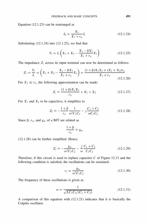
FEEDBACK AND BASIC CONCEPTS 491
Equation (12.1.23) can be rearranged as
Ib = X1
X1 + rπ
Ii (12.1.24)
Substituting (12.1.24) into (12.1.22), we find that
Vi = Ii
(X1 + X2 − X1 − βX2
X1 + rπ
X1
)(12.1.25)
The impedance Zi across its input terminal can now be determined as follows:
Zi = Vi
Ii
=(
X1 + X2 − X1 − βX2
X1 + rπ
X1
)= (1 + β)X1X2 + (X1 + X2)rπ
X1 + rπ
(12.1.26)
For X1 rπ, the following approximation can be made:
Zi ≈ (1 + β)X1X2
rπ
+ X1 + X2 (12.1.27)
For X1 and X2 to be capacitive, it simplifies to
Zi ≈ −1 + β
rπ
1
ω2C1C2− j
C1 + C2
ωC1C2(12.1.28)
Since β, rπ, and gm of a BJT are related as
1 + β
rπ
≈ gm
(12.1.28) can be further simplified. Hence,
Zi ≈ − gm
ω2C1C2− j
ω
C1 + C2
C1C2(12.1.29)
Therefore, if this circuit is used to replace capacitor C of Figure 12.13 and thefollowing condition is satisfied, the oscillations can be sustained:
r1 = gm
ω2C1C2(12.1.30)
The frequency of these oscillations is given as
ω = 1√LC1C2/(C1 + C2)
(12.1.31)
A comparison of this equation with (12.1.21) indicates that it is basically theColpitts oscillator.

492 OSCILLATOR DESIGN
On the other hand, if X1 and X2 are inductive, (12.1.27) gives the relation
Zi ≈ −gmω2L1L2 + jω(L1 + L2) (12.1.32)
Now, if this circuit replaces inductor L of Figure 12.13 and the condition
r1 = gmω2L1L2 (12.1.33)
is satisfied, sustained oscillations are possible. The frequency of these oscilla-tions is
ω = 1√C(L1 + L2)
(12.1.34)
This is identical to (12.1.20), the Hartley oscillator frequency.
12.2 CRYSTAL OSCILLATORS
Quartz and ceramic crystals are used in oscillator circuits for additional stabilityof frequency. They provide a fairly high Q value (on the order of 100,000)that shows a small drift with temperature (on the order of 0.001% per C). Asimplified electrical equivalent circuit of a crystal is illustrated in Figure 12.16.As this equivalent circuit indicates, the crystal exhibits both series and parallelresonant modes. For example, the terminal impedance of a crystal with typicalvalues of CP = 29 pF, LS = 58 mH, CS = 0.054 pF, and RS = 15 exhibits adistinct minimum and maximum with frequency, as shown in Figure 12.17. Itsprimary characteristics may be summarized as follows:
ž The magnitude of the terminal impedance decreases up to around 2.844 MHzwhile its phase angle remains constant at −90. Hence, it is effectively acapacitor in this frequency range.
ž The magnitude of the impedance dips around 2.844 MHz and its phase anglegoes through a sharp change from −90 to 90. It has series resonance atthis frequency.
LS
CS
RS
CP
Figure 12.16 Equivalent circuit of a crystal.

CRYSTAL OSCILLATORS 493
2.842 2.844 2.846
(b)
2.848 2.85
−1.5
−1
−0.5
0.5
1
1.5
Phase angle (deg)
2.84 2.842 2.844 2.846
(a)
2.848 2.85Frequency (MHz)
Frequency (MHz)
100
1,000
10,000
100,000
|Z|
Figure 12.17 Magnitude (a) and phase angle (b) of the terminal impedance as a functionof frequency.
ž The magnitude of the impedance has a maximum around 2.8465 MHz, whereits phase angle changes back to −90 from 90. It exhibits a parallel reso-nance around this frequency.
ž The phase angle of the impedance remains constant at 90 in the frequencyrange 2.844 to 2.8465 MHz while its magnitude increases. Hence, it is effec-tively an inductor.
ž Beyond 2.8465 MHz, the phase angle stays at −90 while its magnitudegoes down with frequency. Therefore, it is changed back to a capacitor.
Series resonant frequency ωS and parallel resonant frequency ωP of the crystalcan be found from its equivalent circuit. These are given as follows:
ωS = 1√LSCS
(12.2.1)
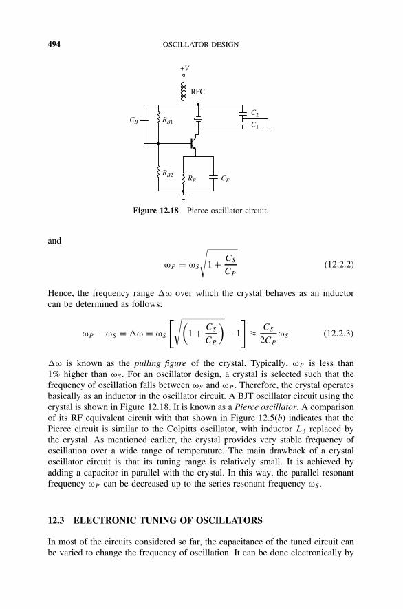
494 OSCILLATOR DESIGN
+V
CE RE
CB RB1
RB2
C2
RFC
C1
Figure 12.18 Pierce oscillator circuit.
and
ωP = ωS
√1 + CS
CP
(12.2.2)
Hence, the frequency range ω over which the crystal behaves as an inductorcan be determined as follows:
ωP − ωS = ω = ωS
[√(1 + CS
CP
)− 1
]≈ CS
2CP
ωS (12.2.3)
ω is known as the pulling figure of the crystal. Typically, ωP is less than1% higher than ωS . For an oscillator design, a crystal is selected such that thefrequency of oscillation falls between ωS and ωP . Therefore, the crystal operatesbasically as an inductor in the oscillator circuit. A BJT oscillator circuit using thecrystal is shown in Figure 12.18. It is known as a Pierce oscillator. A comparisonof its RF equivalent circuit with that shown in Figure 12.5(b) indicates that thePierce circuit is similar to the Colpitts oscillator, with inductor L3 replaced bythe crystal. As mentioned earlier, the crystal provides very stable frequency ofoscillation over a wide range of temperature. The main drawback of a crystaloscillator circuit is that its tuning range is relatively small. It is achieved byadding a capacitor in parallel with the crystal. In this way, the parallel resonantfrequency ωP can be decreased up to the series resonant frequency ωS .
12.3 ELECTRONIC TUNING OF OSCILLATORS
In most of the circuits considered so far, the capacitance of the tuned circuit canbe varied to change the frequency of oscillation. It can be done electronically by

ELECTRONIC TUNING OF OSCILLATORS 495
using a varactor diode and controlling its bias voltage. There are two basic typesof varactors: abrupt and hyperabrupt junctions. Abrupt junction diodes providevery high Q values and also operate over a very wide tuning voltage range(typically, 0 to 60 V). These diodes provide an excellent phase noise performancebecause of their high Q value.
Hyperabrupt-type diodes exhibit a quadratic characteristic of the capacitancewith applied voltage. Therefore, these varactors provide a much more lineartuning characteristic than does the abrupt type. These diodes are preferred fortuning over a wide frequency band. An octave tuning range can be covered inless than 20 V. The main disadvantage of these diodes is that they have a muchlower Q value, and therefore the phase noise is higher than that obtained fromthe abrupt junction diodes.
The capacitance of a varactor diode is related to its bias voltage as follows:
C = A
(VR + VB)n(12.3.1)
A is a constant, VR the applied reverse bias voltage, and VB the built-in potential,0.7 V for silicon diodes and 1.2 V for GaAs diodes. For the following analysis,we can write
C = A
V n(12.3.2)
In this equation, A represents capacitance of the diode when V is 1 V. Also,n is a number between 0.3 and 0.6 but can be as high as 2 for a hyperabruptjunction. The resonant circuit of a typical voltage-controlled oscillator (VCO)has a parallel tuned circuit consisting of inductor L, fixed capacitor Cf , and thevaractor diode with capacitance C. Therefore, its frequency of oscillation can bewritten as
ω = 1√L(Cf + C)
= 1√L
(Cf + A/V n
) (12.3.3)
Let ω0 be the angular frequency of an unmodulated carrier and V0 and C0 be thecorresponding values of V and C. Then
ω20 = 1
L(Cf + C0)= 1
L(Cf + A/V n
0
) (12.3.4)
Further, the carrier frequency deviates from ω0 by δω for a voltage change ofδV . Therefore,
(ω0 + δω)2 = 1
L[Cf + A/(V0 + δV )n]⇒ (ω0 + δω)−2
= L[Cf + A(V0 + δV )−n] (12.3.5)
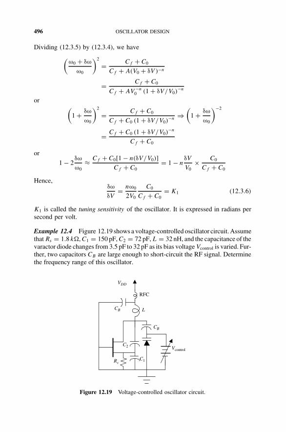
496 OSCILLATOR DESIGN
Dividing (12.3.5) by (12.3.4), we have(ω0 + δω
ω0
)2
= Cf + C0
Cf + A(V0 + δV )−n
= Cf + C0
Cf + AV −n0 (1 + δV/V0)
−n
or (1 + δω
ω0
)2
= Cf + C0
Cf + C0 (1 + δV/V0)−n
⇒(
1 + δω
ω0
)−2
= Cf + C0 (1 + δV/V0)−n
Cf + C0
or
1 − 2δω
ω0≈ Cf + C0[1 − n(δV/V0)]
Cf + C0= 1 − n
δV
V0× C0
Cf + C0
Hence,δω
δV= nω0
2V0
C0
Cf + C0= K1 (12.3.6)
K1 is called the tuning sensitivity of the oscillator. It is expressed in radians persecond per volt.
Example 12.4 Figure 12.19 shows a voltage-controlled oscillator circuit. Assumethat Rs = 1.8 k, C1 = 150 pF, C2 = 72 pF, L = 32 nH, and the capacitance of thevaractor diode changes from 3.5 pF to 32 pF as its bias voltage Vcontrol is varied. Fur-ther, two capacitors CB are large enough to short-circuit the RF signal. Determinethe frequency range of this oscillator.
Rs
RFC
VDD
CB
CB
C2
C1
Vcontrol
L
Figure 12.19 Voltage-controlled oscillator circuit.

PHASE-LOCKED LOOP 497
SOLUTION From (12.1.31),
f = 1
2π√
LCHz
where
C = Cvar + C1C2
C1 + C2
For the varactor capacitance Cvar = 3.5 pF, C is calculated as 52.15 pF and thecorresponding frequency is found to be 123.2 MHz. When Cvar is 32 pF, C isfound as 80.65 pF that gives f as 99.07 MHz. Therefore, the frequency range ofthis oscillator is 99.07 to 123.2 MHz.
12.4 PHASE-LOCKED LOOP
A phase-locked loop (PLL) is a feedback system that is used to lock the outputfrequency and phase to the frequency and phase of a reference signal at its input.The reference waveform can be of many different types, including sinusoidaland digital. PLLs have been used for various applications, including filtering,frequency synthesis, motor speed control, frequency modulation, demodulation,and signal detection. The basic PLL consists of a voltage-controlled oscillator(VCO), a phase detector (PD), and a filter. In its most general form, the PLLmay also contain a mixer and a frequency divider, as shown in Figure 12.20.In the steady state, the output frequency is expressed as follows:
fo = fm ± Nfr (12.4.1)
Hence, the output frequency can be controlled by varying N , fr , or fm.It is helpful to consider the PLL in terms of phase rather than frequency. This
is done by replacing fo, fm, and fr with θo, θm, and θr , respectively. Further,the transfer characteristics of each building block need to be formulated beforethe PLL can be analyzed.
PD Loop filter VCO
Divide byN
fr
ff
fm
fo
Figure 12.20 Block diagram of a PLL system.

498 OSCILLATOR DESIGN
Phase Detector
With the loop in lock, the output of the phase detector is a direct voltage Ve
that is a function of the phase difference θd = θr − θf . If input frequency fr
is equal to ff , Ve must be zero. In commonly used analog phase detectors,Ve is a sinusoidal, triangular, or sawtooth function of θd . It is equal to zerowhen θd is equal to π/2 for the sinusoidal and triangular types, and π for thesawtooth type. Therefore, it is convenient to plot Ve versus a shifted angle θe asshown in Figures 12.21 to 12.23 for a direct comparison of these three types ofdetectors. Hence, the transfer characteristic of a sinusoidal-type phase detectorcan be expressed as follows:
Ve = A sin θe − π
2≤ θe ≤ π
2(12.4.2)
This can be approximated around θe ≈ 0 by the expression
Ve ≈ Aθe
A
−π/2
π/2
θe
θe = θd − π/2
−π π0
Figure 12.21 Sinusoidal output of the PD.
A
−π/2θe
θe = θd − π/2
−π π/2
Figure 12.22 Triangular wave.

PHASE-LOCKED LOOP 499
A
θe = θd − π
−π π0 θe
Figure 12.23 Sawtooth wave.
In the case of a triangular output of the phase detector, the transfer characteristiccan be expressed as
Ve = 2A
πθe − π
2≤ θe ≤ π
2(12.4.3)
From the transfer characteristic of the sawtooth-type phase detector illustrated inFigure 12.23, we can write
Ve = A
πθe − π ≤ θe ≤ π (12.4.4)
Since Ve is zero in steady state, the gain factor Kd (volts per radians) in all threecases is
Ve
θe
= Kd (12.4.5)
Voltage-Controlled Oscillator
As described earlier, a varactor diode is generally used in the resonant circuitof an oscillator. Its bias voltage is controlled to change the frequency of oscilla-tion. Therefore, the transfer characteristic of an ideal voltage-controlled oscillator(VCO) has a linear relation, as depicted in Figure 12.24. Hence, the output fre-quency of a VCO can be expressed as follows:
fo = fS + koVd Hz
orω0 = ωS + KoVd rad/s

500 OSCILLATOR DESIGN
fo
fS
Vd
Figure 12.24 Characteristic of a voltage-controlled oscillator.
or
ω0 = ωS + δω rad/s
θ(t) =∫ t
0ω0dt = ωSt +
∫ t
0δωdt = θS + θ0(t)
Therefore,
θ0(t) =∫ t
0δωdt ⇒ dθ0(t)
dt= δω = KoVd (12.4.6)
In the s-domain,
sθ0(s) = KoVd(s) ⇒ θ0(s)
Vd(s)= Ko
s
Hence, VCO acts as an integrator.
Loop Filters
A low-pass filter is connected right after the phase detector to suppress its outputharmonics. Generally, it is a simple first-order filter. Sometimes higher-orderfilters are also employed to suppress additional ac components. The transfercharacteristics of selected loop filters are summarized below.
Lead–Lag Filter. A typical lead–lag filter uses two resistors and a capacitor,as illustrated in Figure 12.25. Its transfer function, F(s), can be found as follows:
Vo
Vi
= R2 + 1/sC2
R1 + R2 + 1/sC2= 1 + sR2C2
1 + s(R1C2 + R2C2)
Hence,
F(s) = 1 + τ2s
1 + τ1s(12.4.7)

PHASE-LOCKED LOOP 501
R1
C2
VoVi
R2
Figure 12.25 Lead–lag filter.
where
τ2 = R2C2 (12.4.8)
and
τ1 = (R1 + R2)C2 (12.4.9)
Typical magnitude and phase characteristics versus frequency (the Bode plot) ofa lead–lag filter are illustrated in Figure 12.26. The time constants τ1 and τ2
used to draw these characteristics were 0.1 and 0.01 s, respectively. Note that thechanges in these characteristics occur at 1/τ1 and 1/τ2.
Integrator and Lead Filter. This type of filter generally requires an op ampalong with two resistors and a capacitor. As illustrated in Figure 12.27, the feed-back path of the op amp uses a capacitor in series with resistance. Assumingthat the op amp is ideal and is being used in inverting configuration, the transfercharacteristics of this filter can be found as follows:
Vo
Vi
= −R2 + 1/sC2
R1= −1 + sR2C2
sR1C2
F(s) = 1 + sτ2
sτ1(12.4.10)
where
τ1 = R1C2 (12.4.11)
and
τ2 = R2C2 (12.4.12)
Typical frequency response characteristics (the Bode plot) of an integrator andlead filter are illustrated in Figure 12.28. Time constants τ1 and τ2 used for thisillustration are 0.1 and 0.01 s, respectively.
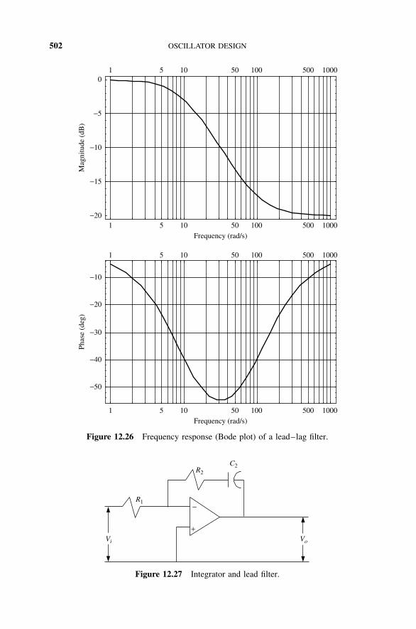
502 OSCILLATOR DESIGN
−50
−40
−30
−20
−10
Frequency (rad/s)
−20
−15
Mag
nitu
de (
dB)
Phas
e (d
eg)
−10
−5
01 5 10 50 100 500 1000
1 5 10 50 100 500 1000
1 5 10 50 100 500 1000
Frequency (rad/s)1 5 10 50 100 500 1000
Figure 12.26 Frequency response (Bode plot) of a lead–lag filter.
Vi
R1
R2
C2
+
−
Vo
Figure 12.27 Integrator and lead filter.

PHASE-LOCKED LOOP 503
−80
−60
−40
−20
Frequency (rad/s)
−20
Mag
nitu
de (
dB)
Phas
e (d
eg)
−10
0
10
201 5 10 50 100 500 1000
1 5 10 50 100 500 1000
1 5 10 50 100 500 1000
Frequency (rad/s)
1 5 10 50 100 500 1000
Figure 12.28 Frequency response (Bode plot) of integrator and lead filter.
Note again that there are significant changes occurring in these characteristicsat frequencies that are equal to 1/τ1 and 1/τ2. For frequencies less than 10 rad/s,the phase angle is almost constant at −90, whereas the magnitude changes ata rate of 20 dB/decade. It represents the characteristics of an integrator. Thephase angle becomes zero for frequencies greater than 100 rad/s. The magnitudebecomes constant at −20 dB as well.
Integrator and Lead–Lag Filter. Another active filter that is used in the loopis shown in Figure 12.29. It employs two capacitors in the feedback loop of theop amp. Assuming again that the op amp is ideal and is connected in inverting

504 OSCILLATOR DESIGN
Vi
R1
R2
C2
C1
+
−
Vo
Figure 12.29 Integrator and lead–lag filter.
configuration, the transfer function of this filter can be found as follows:
Vo
Vi
= − 1
R1
(R2/sC2
R2 + 1/sC2+ 1
sC1
)= − 1
R1
(R2
1 + sR2C2+ 1
sC1
)
= − R2/R1
1 + sR2C2− 1
sR1C1
orVo
Vi
= − sR2C1 + 1 + sR2C2
sR1C1(1 + sR2C2)
This can be rearranged as follows:
F(s) = − 1
sτ1
1 + sτ2
1 + sτ3(12.4.13)
where
τ1 = C1R1 (12.4.14)
τ2 = R2(C1 + C2) (12.4.15)
and
τ3 = R2C2 (12.4.16)
The frequency response of a typical integrator and lead–lag filter is shown inFigure 12.30. Time constants τ1, τ2, and τ3 are assumed to be 1, 0.1, and 0.01 s,respectively. The corresponding frequencies are 1, 10, and 100 rad/s. At frequen-cies below 1 rad/s, the magnitude of the transfer function decreases at a rate of20 dB/decade while its phase angle stays at −90. Similar characteristics may be

PHASE-LOCKED LOOP 505
−80
−70
−60
−50
−40
Frequency (rad/s)
−40
Mag
nitu
de (
dB)
Phas
e (d
eg)
−30
−20
−10
01 5 10 50 100 500 1000
1 5 10 50 100 500 1000
1 5 10 50 100 500 1000
Frequency (rad/s)
1 5 10 50 100 500 1000
Figure 12.30 Frequency response (Bode plot) of integrator and lead–lag filter.
observed above 100 rad/s. It is a typical integrator characteristic. A significantchange in the frequency response may be observed at 10 rad/s as well.
An equivalent block diagram of the PLL can be drawn as shown in Figure 12.31.Output θo of the VCO can be controlled by voltage V , reference signal θr , ormodulator input θm. To understand the working of the PLL when it is nearly locked,the transfer function for each case can be formulated with the help of the figure.
A general formula for the transfer function T (s) of a single-feedback-loopsystem can be written with the help of Figure 12.1:
T (s) = forward gain
1 + loop gain(12.4.17)

506 OSCILLATOR DESIGN
Kd F(s)
V
Kos
1 1N
θr
θm
θ0
Figure 12.31 Equivalent block diagram of a PLL.
Since there are three different ways to control the phase of the VCO, the transferfunction for each case can be found via (12.4.17), as follows:
1. When phase θm of the mixer input controls the VCO output θo, its transferfunction T1(s) is found to be
T1(s) = θo(s)
θm(s)= (1/N)KdF (s)(Ko/s)
1 + (1/N)KdF (s)(Ko/s)1= KF(s)
s + KF(s)(12.4.18)
where
K = KdKo
N(12.4.19)
2. When phase θr of the reference input controls the output θo of the VCO,its transfer function T2(s) will be
T2(s) = θo(s)
θr (s)= KdF(s)Ko/s
1 + K[F(s)/s]= NKF(s)
s + KF(s)(12.4.20)
3. Similarly, for the case of input voltage V controlling θo, its transfer functionT3(s) is found to be
T3(s) = θo(s)
V= Ko/s
1 + K[F(s)/s]= Ko
s + KF(s)(12.4.21)
It is obvious from (12.4.18) to (12.4.21) that the transfer function F(s) ofthe filter significantly affects the working of a PLL. Various types of loop filtershave been used to obtain the desired PLL characteristics, including the three loopfilters described earlier: the lead–lag filter, an integrator in combination with alead network, and an integrator combined with a lead–lag network. The numberof poles of the loop gain [KF(s)/s] at the origin determines the type of phase-locked loop. Hence, a phase-locked loop with a passive lead–lag filter (withouta charge pump) is of type 1 because its loop gain has only one pole at the origin.

PHASE-LOCKED LOOP 507
Phase-detector output is a voltage that drives the loop filter. There is a significantimprovement in performance if a current source (or sink) drives the loop filter.There is a double pole at the origin if either of the remaining two filters is used(an integrator in combination with a lead or a lead–lag network). Therefore, it isa type 2 phase-locked loop now because the integrator adds another pole at theorigin. Further, the highest degree of the characteristic polynomial equation [1+KF (s)/s = 0] is called the order of that phase-locked loop. Hence, if a PLL isemploying the passive lead–lag filter of Figure 12.25, it is a second-order type1 system. On the other hand, it will be second-order type 2 with the integratorand lead filter of Figure 12.27, and third-order type 2 with the integrator andlead–lag filter shown in Figure 12.29.
Equations (12.4.18) to (12.4.21) are used to analyze the stability of a PLL andto develop the relevant design procedures. As an example, consider the casewhere a lead–lag filter is being used and the frequency divider is excluded fromthe loop (i.e., N = 1). The transfer function T2(s) for this PLL can be obtainedby substituting (12.4.7) into (12.4.20) as follows:
T2(s) = Kv(1 + τ2s)
s(1 + τ1s) + Kv(1 + τ2s)
where Kv = KdKo is the dc gain of the loop.Generally, T2(s) is rearranged in the following form for further analysis of
the PLL.
T2(s) = ω2n + (2ζωn − ω2
n/Kv)s
s2 + 2ζωns + ω2n
Coefficients ωn and ζ are called the natural frequency and the damping factor,respectively. These are defined as
ωn =√
Kv
τ1
and
ζ = ωn
2
(τ2 + 1
Kv
)
These coefficients must be selected such that the PLL is stable and performs accord-ing to the specifications. See Table 12.1 for a summary of PLL components.
Phase-Locked-Loop Terminology
Hold-in Range. This is also called the lock range, the tracking range, or thesynchronization range. If reference frequency fr is changed slowly from thefree-running frequency ff , VCO frequency fo tracks fr until the phase errorθe approaches ±π/2 for sinusoidal and triangular phase detectors or ±π for a

508 OSCILLATOR DESIGN
TABLE 12.1 Summary of PLL Components
Element Transfer Function Remarks
VCOKo
sKo is the slope of the oscillator frequency to the
voltage characteristic. It is expressed in radians persecond per volt.
Mixer 1 The change of output phase equals the change ofinput phase.
Divider1
NN is the division ratio.
Phase detector Kd Kd is the slope of the phase detector voltage to thephase characteristic in volts per radian.
Filter F(s) The transfer function depends on the type of filterused.
sawtooth-type phase detector. It is assumed here that the VCO is capable ofsufficient frequency deviation and that the loop filter and amplifier (if any) arenot overdriven.
From the transfer function of a sinusoidal phase detector as given by (12.4.2),we find that
sin θe = Ve
Kd
The output voltage Ve of the phase detector is applied to the input of the voltage-controlled oscillator. Therefore, using (12.4.6) with Vd = Ve,
sin θe = Ve
Kd
= δω
KoKd
(12.4.22)
Since θe ranges between −90 and +90, the hold-in range, δωH , for this caseis found to be
δωH = ±KdKo (12.4.23)
Hence, if there is no frequency divider in the loop (i.e., N = 1), the hold-in rangeis equal to dc loop gain.
Similarly, the hold-in range with a triangular or sawtooth phase detector withlinear characteristics can be determined via (12.4.3) to (12.4.5). It may be found as
δωH = ±KdKoθe max (12.4.24)
Note that θe max is π/2 for triangular and π for sawtooth phase detectors.
Example 12.5 Free-running frequency and the gain factor of a voltage-controlledoscillator are given as 100 MHz and 100 kHz/V, respectively. It is being used ina PLL along with a sinusoidal phase detector with a maximum output of 2 V at

PHASE-LOCKED LOOP 509
θe = π/2 radians. If there are no amplifiers or frequency divider in the loop, whatis its hold-in range?
SOLUTION From (12.4.2),
Kd = Ve
sin θe
= 2
Similarly, from the voltage-controlled oscillator characteristics,
Ko = δω
Vd
= 2π × 100 × 1000 rad/s · V
Hence,
δωH = ±2 × 2π × 105 rad/s
or
δfH = ±200 kHz
Example 12.6 If the phase detector in Example 12.5 is replaced by a triangulartype with Ve max = A = 2 V at θe max = π/2 radians, find the new holding range.
SOLUTION From (12.4.5),
Kd = 2
π/2= 4
π
Since the voltage-controlled oscillator is still the same, Ko = 2π × 105 rad/s ·V.Hence, the new hold-in range will be given as follows:
δωH = 4
π× 2π × 105 × π
2= 4π × 105 rad/s
orδfH = 200 kHz.
Acquisition of Lock. Suppose that a signal with frequency fr is applied to theloop as shown in Figure 12.20. If this frequency is different from the feedbacksignal frequency ff , the loop tries to capture or acquire the signal. Two frequen-cies are equalized if the initial difference is not too large. In general, maximumradian frequency difference ±(ωr − ωf ) must be smaller than the hold-in range.Acquisition of lock is a nonlinear process whose description is beyond the scopeof this chapter. Some general conclusions based on a commonly used lead–lagfilter are summarized below.

510 OSCILLATOR DESIGN
Lock-in Range. If the frequency difference |ωr − ωf | is less than a 3-dB band-width of closed-loop transfer function T2(s), the loop locks up without slippingcycles. The maximum lock-in range, δωL, may be found by the formula
δωL = ±Kτ2
τ1(12.4.25)
K is the dc loop gain, τ1 = (R1 + R2)C2, and τ2 = R2C2, as defined earlier. Thelock-in range can be expressed in terms of natural frequency ωn and dampingfactor ζ of closed-loop transfer function T2(s) with a lead–lag filter. It is givenas follows:
δωL ≈ ±2ζωn (12.4.26)
where
ωn =√
K
τ1(12.4.27)
and
ζ = ωn
2
(τ2 + 1
K
)(12.4.28)
Pull-in Range. Suppose that frequency difference |ωr − ωf | is initially outsidethe lock-in range but is inside the pull-in range. In this case, the differencefrequency signal at the output of the phase detector is nonlinear and contains adc component that gradually shifts the VCO frequency fo(ff = fo/N) toward fr
until lock-in occurs. For high-gain loops, an approximate formula for the pull-inrange is
δωP ≈ ±√
2(2ζωnK − ω2n) (12.4.29)
It is desirable for the loop to have a large bandwidth that helps in capture initially.However, it increases the transmission of noise. These contradictory conditionsmay be satisfied in two different ways:
1. Use a larger bandwidth initially but reduce it after the lock is acquired.
2. Use a small bandwidth but sweep the frequency of the voltage-controlledoscillator until the lock is acquired.
Example 12.7 In the PLL shown in Figure 12.32, peak amplitudes of the refer-ence input and VCO output are both 0.75 V. An analog multiplier is being usedas a phase detector that has a 2-V output when its reference input, Vin, and theoscillator signal, Vosc, are both 2 V. The free-running frequency of the VCO is10 MHz, which reduces to zero when its control voltage Vcntl is reduced by 1 V.

PHASE-LOCKED LOOP 511
PD F(s) VCO
Vosc
Vin VPD Vd
Figure 12.32 PPL for Example 12.7.
Find the phase difference between the input and VCO output when it is in lockwith an input frequency of (a) 11 MHz and (b) 9 MHz.
SOLUTION Since the output of an analog multiplier is proportional to theproduct of its two inputs, we can write
VPD = KmVinVosc
Hence, the proportionality constant Km is
Km = 2
2 × 2= 0.5 V−1
For
Vin = Ein sin ωt
and
Vosc = Eosc cos(ωt − φd)
VPD = KmEinEosc sin ωt cos(ωt − φd)
= 0.5KmEinEosc[sin φd + sin(2 ωt − φd)]
Since the output of the phase detector is passed through a low-pass filter beforeit is applied to the voltage-controlled oscillator, the controlling voltage Vd maybe written as
Vd = 0.5KmEinEosc sin φd ≈ 0.5KmEinEoscφd
Hence, the transfer function Kd is
Kd = Vd
φd
= 0.5KmEinEosc = 0.5 × 0.5 × 0.752 = 0.1406 V/rad
Transfer function Ko of the voltage-controlled oscillator can be found from (12.4.6)as
Ko = δω
Vd
= 2π × 107
1= 2π × 107 rad/s · V

512 OSCILLATOR DESIGN
Since the output frequency of the voltage-controlled oscillator is given as
ω0 = KoVd + ωs = ωin
we can write
Vd = ωin − ωs
Ko
Hence,
φd = Vd
Kd
= ωin − ωs
KoKd
(a) The input signal frequency in this case is 11 MHz while the free-runningfrequency of the voltage-controlled oscillator is 10 MHz. Hence,
φd = 2π(11 MHz − 10 MHz)
KoKd
= 0.7111 rad = 40.74
Since there is a constant phase shift of 90 that is always present, actual phasedifference between the input signal and the output of VCO will be 90 − 40.74 =49.26.
(b) Since the input signal frequency in this case is 9 MHz, we find that
φd = 2π(9 MHz − 10 MHz)
KoKd
= −0.7111 rad = −40.74
As before, because of a constant phase shift of 90, the actual phase differencebetween the input signal and the output of the VCO will be 90 + 40.74 =130.74.
Further Analysis of the PLL
Consider the simplified block diagram of the PLL shown in Figure 12.33. Itconsists of only a phase detector, a low-pass filter, and a voltage-controlledoscillator. Assume that the reference and the output signals are vr and vo, respec-tively. Hence,
vr(t) = Ar sin[ωt + θr (t)] (12.4.30)
PD F(s) VCO vr(t)
vo(t)
vo(t)
v1(t) v2(t)
Figure 12.33 Simplified block diagram of a PLL.

PHASE-LOCKED LOOP 513
and
vo(t) = Ao cos[ωt + θo(t)] (12.4.31)
Note that output frequency of the VCO varies with v2(t); therefore,
θo(t) = Ko
∫ t
v2(τ)dτ (12.4.32)
Ko is in radians per second per volt, as defined earlier. The output of the phasedetector is
v1(t) = Kmvr(t)vo(t) = KmArAo sin[ωt + θr (t)] cos[ωt + θo(t)]
or
v1(t) = KmArAo
2sin[θr (t) − θo(t)] + sin[2 ωot + θr (t) + θo(t)] (12.4.33)
The low-pass filter stops the sum frequency component (the second term). Hence,
v2(t) = Kd sin[θe(t)] ⊗ f (t) (12.4.34)
where ⊗ represents the convolution of two terms, θe(t) is equal to θr (t) − θo(t),and Kd is equal to 0.5KmArAo.
The overall equation describing the operation of the PLL may be found asfollows:
dθe(t)
dt= dθr (t)
dt− dθo(t)
dt= dθr (t)
dt− d
dt
KdKo
∫ t
sin[θe(τ)] ⊗ f (τ)dτ
or
dθe(t)
dt= dθr (t)
dt− KdKo sin[θe(t)] ⊗ f (t) (12.4.35)
For sin[θe(t)] ≈ θe(t), (12.4.35) can be approximated as
dθe(t)
dt≈ dθr (t)
dt− KdKoθe(t) ⊗ f (t)
Taking the Laplace transform of this equation with initial conditions as zero, itcan be transformed into the frequency domain. Hence,
sθe(s) = sθr (s) − KdKoθe(s)F (s)
or[s + KdKoF (s)][θr (s) − θo(s)] = sθr (s)
orKdKoF (s)θr (s) = [s + KdKoF (s)]θo(s)

514 OSCILLATOR DESIGN
Hence, the closed-loop transfer function T (s) is
T (s) = θo(s)
θr (s)= KdKoF (s)
s + KdKoF (s)(12.4.36)
This is identical to (12.4.20) if the frequency division is assumed as unity.
Example 12.8 Analyze the PLL system shown in Figure 12.34. By controllingthe frequency divider, its output frequency can be changed from 2 MHz to 3 MHzin steps of 100 kHz. Transfer function of the phase detector, Kd , is 0.5 V/rad.Free-running frequency and a gain factor of VCO are 2.5 MHz and 107 rad/s·V,respectively. A voltage gain of the amplifier is 10. Design a passive lead–laglow-pass filter that can be used in the loop.
SOLUTION With fm as zero (i.e., without the mixer), the output frequency isfound from (12.4.1) as
fo = Nfr
Since it has a resolution of 100 kHz, its reference frequency must be the same.Next, the range of N is determined from the equation above and the desiredfrequency band. For fo to be 2 MHz, N must be equal to 20. Similarly, it is 30for an output frequency of 3 MHz. Hence,
20 ≤ N ≤ 30
From (12.4.6),
Vd = ωo − ωf
Ko
= 2π
107(2 × 10⁶ − 2.5 × 10⁶) = − π
10V
Going back around the loop, input to the amplifier (or output of the phase detec-tor) can be found as
Ve = Vd
Ka
= − π
100V
fr foVe Vd
Phase detector Low-pass
filter
Voltage-controlledoscillator
AmplifierKa = 10
Frequencydivider
θe = θo/N θo
1N
Figure 12.34 PPL for Example 12.8.

PHASE-LOCKED LOOP 515
and the output of the frequency divider may be found from (12.4.5) as follows:
θe = Ve
Kd
= − π
50rad
Therefore, θo at the output frequency of 2 MHz is given as follows:
θo = −2
5π = −1.2566 rad
The dc loop gain K can be found via (12.4.19) as
K = KdKaKo
N= 0.5 × 10 × 107
20= 2.5 × 10⁶
The pull-in range δωp is given by (12.4.29) assuming that K ωn.For ωn = 104 rad/s and ζ = 0.8, the pull-in range is
δω ≈ 2.8249 × 10⁵ rad/s
or
δfp = 4.5 × 10⁴ Hz = 45 kHz
A lag–lead filter can be designed as follows. From (12.4.27),
τ1 = K
ω2n
= 2.5 × 10⁶
108= 0.025 s = (R1 + R2)C2
and from (12.4.28),
ζ = ωn
2
(τ2 + 1
K
)⇒ τ2 = 2ζ
ωn
− 1
K= 2 × 0.8
104− 1
2.5 × 106
= 1.596 × 10⁻⁴s = R2C2
For C2 = 0.5 µF,
R2 = 1.596 × 10⁻⁴
0.5 × 10−6= 319.2
and
R1 = τ1
C2− R2 = 0.025
0.5 × 10⁻⁶− 319.2 = 50,000 − 319.2
= 49,680.8 ≈ 50 k

516 OSCILLATOR DESIGN
12.5 FREQUENCY SYNTHESIZERS
The frequency of a reference oscillator can be multiplied and its harmonics can begenerated with the help of a nonlinear device. The desired frequency componentcan then be filtered out. This type of frequency generation is called direct synthe-sis. However, it has several limitations, including constraints on the filter design.An alternative approach uses a PLL (analog or digital) to synthesize the desiredsignal. This is known as indirect synthesis. Another technique, known as directdigital synthesis (DDS), uses a digital computer and a digital-to-analog converterfor generating the desired signal. In this section we consider indirect frequencysynthesis. Mixers and frequency multipliers are described in Chapter 13.
Example 12.8 illustrated the basic principle of an indirect frequency synthe-sizer. A simplified PLL frequency synthesizer is illustrated in Figure 12.35. Asdiscussed in Section 11.4, the feedback signal frequency fd is equal to the refer-ence frequency fr if the loop is in the locked state. Since the frequency dividerdivides the output frequency by N , the output frequency fo is equal to Nfr . IfN is an integer, the frequency step is equal to reference frequency fr . For a fineresolution, the reference frequency should be very low. On the other hand, lowerfr increases the switching time. As a rule of thumb, the product of switchingtime ts and the reference frequency fr is equal to 25. Therefore, the switchingtime is 25 s for the reference frequency of 1 Hz. Since a shorter switching timeis desired, it limits the frequency resolution of this system.
As illustrated in Figure 12.36, one way to improve the frequency resolutionwhile keeping the switching time short (the reference frequency high) is to add
fr foVe
Phase detector Low-pass
filter
Voltage-controlledoscillator
Frequencydivider
fd = fo/Nfo1
N
Figure 12.35 PLL frequency synthesizer.
fr foPhase detector Low-pass
filter
Voltage-controlledoscillator
Frequencydivider
Frequencydivider
1N
1M
Figure 12.36 PLL followed by a frequency divider.

FREQUENCY SYNTHESIZERS 517
another frequency divider at its output. Hence, the output frequency in this systemwill be given as
fo = Nfr
M(12.5.1)
Thus, the frequency resolution in this system is fr/M , which shows an improve-ment over the previous arrangement. However, a close analysis of this systemindicates that the signal frequency in its phase-locked-loop section may becomeexcessively large. This is explained further via the following example.
Example 12.9 Design a PLL frequency synthesizer that covers the frequencyrange from 100 to 110 MHz with a resolution of 1 kHz.
SOLUTION With the single loop of Figure 12.35, the reference frequency mustbe equal to the resolution required. Hence,
fr = 1 kHz
Since the output frequency fo = Nfr , the range of N is
105 ≤ N ≤ 11 × 104
As explained earlier, the switching time in this case is on the order of 25 ms. Ifthis switching time is not acceptable and we want to keep it below 250 µs, anarrangement similar to that illustrated in Figure 12.36 may be used. A referencefrequency of 100 kHz provides the switching time of 250 µs. In this case, settingM of the output frequency can be determined as
M = fr
frequency resolution= 100 kHz
1 kHz= 100
To cover the desired frequency range, the voltage-controlled oscillator must gen-erate frequencies from 10 to 11 GHz. This is because the frequency dividerdivides output of the voltage-controlled oscillator by M before the signal appear-ing at the output.
The range of N can be determined after dividing the frequency of the voltage-controlled oscillator by the reference frequency. Hence,
105 ≤ N ≤ 11 × 104
Thus, this may not be a good technique to get better frequency resolution. How-ever, this concept is extended in practice where multiple loops are used to obtainfine resolution. It is illustrated through the following example.
Example 12.10 Design a PLL frequency synthesizer for the frequency range 1to 50 MHz with increments of 1 kHz.

518 OSCILLATOR DESIGN
SOLUTION Note that if a single-loop synthesizer is used in this case, its ref-erence frequency should be of 1 kHz. That makes its switching time on the orderof 0.025 s and the setting of frequency-divider ranges as
1 × 10³ ≤ N ≤ 50 × 103
An alternative design that uses three phase-locked loops is illustrated inFigure 12.37. Loops A and B use a higher-reference frequency (say, 100 kHz),while the output of A (fA) works as the reference for loop C after it is dividedby M . The following relation holds when the loops are in the locked state:
fA = fo − fB
Therefore, the output frequency fo is equal to the sum of other two, fA and fB.
Frequencydivider
Frequencydivider
M1
fr fA
fB
fo − fB
fo
faPhase detector
Phase detector
Low-passfilter
Voltage-controlledoscillator
Low-passfilter
Voltage-controlledoscillator
1NA
Frequencydivider
1NB
Low-pass
filter
Voltage-controlledoscillator
BPF
Phasedetector
Loop C
Loop B
Loop A
Figure 12.37 Multiloop frequency synthesizer system.

FREQUENCY SYNTHESIZERS 519
If a mixer is used to combine fA and fB directly, its sum and differencefrequency components may be too close to separate the two via a bandpass filter.However, the present technique of using a phase-locked loop C for this purposeaccomplishes the desired separation. Since the reference frequency is 100 kHz,the output frequency of loop A, fa , can be varied in steps of 100 kHz, and 1 kHzresolution in the output can be achieved with M as 100. Hence,
fa = 105NA
and
fA = fa
100= 103 × NA
Thus, fA varies in 1-kHz steps. Loop A can generate increments of 1 and 10 kHzin the output frequency. Similarly, loop B produces 0.1- and 1-MHz steps in theoutput frequency. Reference frequency fA to loop C should be selected in such away that it keeps its switching time short. If, for example, fA is equal to 1 kHz,the switching time of loop C is on the order of 0.025 s. Since it is the longesttime among the three loops, it sets the overall response time of the synthesizer.To reduce the response time of loop C, fA may be increased to 500 kHz so that
500 kHz ≤ fA ≤ 599 kHz
Therefore, the output frequency of loop A (i.e., before dividing by 100) rangesas follows:
5 × 10⁷ Hz ≤ fa ≤ 5.99 × 10⁷ Hz
The range of the frequency divider setting, NA, can be determined easily as fa/fr .Hence, 500 ≤ NA ≤ 599. Since fB = fo − fA, fB is reduced by 500 kHz,
(1 − 0.5)MHz ≤ fB ≤ (50 − 0.5)MHz
or0.5 MHz ≤ fB ≤ 49.5 MHz
Hence, the frequency divider setting, NB, in loop B ranges as follows: 5 ≤ NB ≤495. Loops A and B use the same reference frequency and therefore have thesame response time, on the order of 250 µs. On the other hand, loop C hasa response time on the order of 50 µs. Thus, the overall response time of thefrequency synthesizer is approximately 250 µs. At the same time, we achieved afrequency resolution of 1 kHz. This idea can be extended to reduce the frequencyresolution even below 1 kHz while keeping the overall response time short byusing additional loops.

520 OSCILLATOR DESIGN
12.6 ONE-PORT NEGATIVE RESISTANCE OSCILLATORS
Properly biased Gunn and IMPATT (impact ionization avalanche transit time)diodes exhibit negative resistance characteristics that can be utilized in conjunc-tion with an external resonant circuit to design a solid-state microwave oscillator.The Gunn diode is a transferred-electron device that uses a bulk semiconductor(usually, GaAs or InP) as opposed to a p-n junction. Its dc-to-RF conversionefficiency is generally less than 10%.
The IMPATT diode uses a reverse-biased p-n junction to generate microwavepower. The diode material is usually silicon or GaAs, and it is operated with arelatively high voltage, on the order of 70 to 100 V, to achieve a reverse-biasedavalanche breakdown current. When coupled with a high-Q resonator and biasedat an appropriate operating point, the diode exhibits a negative resistance effectand sustained oscillations are obtained. Its output power is much higher (on theorder of tens or hundreds of watts) than that produced by a Gunn diode. On theother hand, Gunn diodes produce relatively low FM noise.
Figure 12.38 shows the RF equivalent circuits for a one-port negative resis-tance oscillator where ZG is the input impedance (YG is the correspondinginput admittance) of the active device (i.e., a biased diode). Figure 12.38(b)is an equivalent parallel arrangement of the circuit shown in Figure 12.38(a).In general, the impedance ZG (or admittance YG) is current (or voltage) andfrequency dependent.
Applying Kirchhoff’s loop equation in the circuit shown in Figure 12.38(a),we get
(ZG + ZL)I = 0
If oscillations are occurring, current I in the loop is nonzero. In such a situation,the following conditions must be satisfied:
RG + RL = 0 (12.6.1)
YG = GG + jBG
Negativeresistancedevice
(a) (b)
I
V XL
RL
RG
XG
ΓG ΓL
GG BG
BL GL
YL = GL + jBL
ZG = RG + jXG ZL = RL + jXL
Figure 12.38 Series (a) and parallel (b) equivalent circuits for one-port negative resis-tance microwave oscillators.
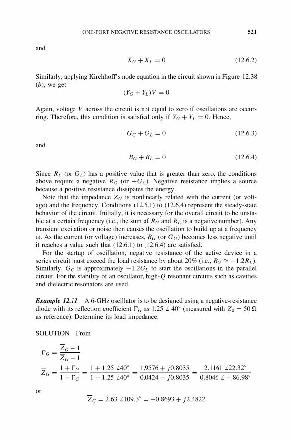
ONE-PORT NEGATIVE RESISTANCE OSCILLATORS 521
and
XG + XL = 0 (12.6.2)
Similarly, applying Kirchhoff’s node equation in the circuit shown in Figure 12.38(b), we get
(YG + YL)V = 0
Again, voltage V across the circuit is not equal to zero if oscillations are occur-ring. Therefore, this condition is satisfied only if YG + YL = 0. Hence,
GG + GL = 0 (12.6.3)
and
BG + BL = 0 (12.6.4)
Since RL (or GL) has a positive value that is greater than zero, the conditionsabove require a negative RG (or −GG). Negative resistance implies a sourcebecause a positive resistance dissipates the energy.
Note that the impedance ZG is nonlinearly related with the current (or volt-age) and the frequency. Conditions (12.6.1) to (12.6.4) represent the steady-statebehavior of the circuit. Initially, it is necessary for the overall circuit to be unsta-ble at a certain frequency (i.e., the sum of RG and RL is a negative number). Anytransient excitation or noise then causes the oscillation to build up at a frequencyω. As the current (or voltage) increases, RG (or GG) becomes less negative untilit reaches a value such that (12.6.1) to (12.6.4) are satisfied.
For the startup of oscillation, negative resistance of the active device in aseries circuit must exceed the load resistance by about 20% (i.e., RG ≈ −1.2RL).Similarly, GG is approximately −1.2GL to start the oscillations in the parallelcircuit. For the stability of an oscillator, high-Q resonant circuits such as cavitiesand dielectric resonators are used.
Example 12.11 A 6-GHz oscillator is to be designed using a negative-resistancediode with its reflection coefficient G as 1.25 40 (measured with Z0 = 50
as reference). Determine its load impedance.
SOLUTION From
G = ZG − 1
ZG + 1
ZG = 1 + G
1 − G
= 1 + 1.25 40
1 − 1.25 40 = 1.9576 + j0.8035
0.0424 − j0.8035= 2.1161 22.32
0.8046 − 86.98
orZG = 2.63 109.3 = −0.8693 + j2.4822

522 OSCILLATOR DESIGN
If a given reflection coefficient has magnitude greater than unity, we can still usea Smith chart to find the corresponding impedance provided that we follow theprocedure described in Section 11.3. Thus, the impedance point can be identifiedon a Smith chart, as shown in Figure 12.39. The corresponding value is foundto be the same as obtained above through the formula. Hence,
ZG = RG + jXG = −43.5 + j124.11
0
0.2
0.5 1 2 5
10
180
170
160
150
140
130120
110 100 90 8070
60
50
40
3020
100
−10−20
−30−40
−50−60
−70−80−90−100−110−120−130
−140
−150
−160
−170
ZG
Figure 12.39 Graphical method of determining the input impedance of the diode.
Load Negativeresistancedevice
j124.11 Ω −j124.11 Ω
43.5 Ω−43.5 Ω
Figure 12.40 Equivalent circuit of Example 12.11.

MICROWAVE TRANSISTOR OSCILLATORS 523
Therefore, the load impedance is given as
ZL = 43.5 − j124.11
The corresponding equivalent circuit is illustrated in Figure 12.40.
12.7 MICROWAVE TRANSISTOR OSCILLATORS
Several oscillator circuits using transistors were considered in Section 12.1 alongwith the basic concepts. In this section we present a design procedure that is basedon the S-parameters of the transistor. The RF circuit arrangement of a microwavetransistor oscillator is shown in Figure 12.41. A field-effect transistor shown asthe device in this figure is in common-source configuration, although any otherterminal can be used in its place, provided that the corresponding S-parametersare known. Further, a BJT can also be used in its place. In other words, thedesign procedure described here is general and applies to any transistor circuitconfiguration as long as its S-parameters are known.
Unlike the amplifier circuit, the transistor for an oscillator design must beunstable. Therefore, the opposite of conditions (11.1.16) and (11.1.18) must holdin this case. If the stability parameter k is not less than unity (or || is notlarger than unity), an external positive feedback can be used to make the deviceunstable. Equations (12.6.1) to (12.6.4) can be recast as follows:
inG = 1 (12.7.1)
or
outL = 1 (12.7.2)
These two conditions state that passive terminations ZG and ZL must be addedfor resonating the input and output ports of the active device at the frequency
Generator tuningnetwork
Load-matchingnetwork
D
S
G
Device
ΓG(ZG) ΓL
(ZL)Γin(Zin)
Γout(Zout)
Figure 12.41 Microwave transistor oscillator circuit.

524 OSCILLATOR DESIGN
of oscillation. These two conditions are complementary to each other [i.e., ifcondition (12.7.1) is satisfied, (12.7.2) is also satisfied, and vice versa]. It can beproved as follows.
From the expression for input reflection coefficient obtained in Example 10.6,we can write
in = S11 + S12S21L
1 − S22L
= S11 − L
1 − S22L
⇒ 1
in= 1 − S22L
S11 − L
(12.7.3)
where = S11S22 − S12S21, as defined in Chapter 11. If (12.7.1) is satisfied, then
G = 1
in= 1 − S22L
S11 − L
⇒ S11G − LG = 1 − S22L ⇒
L = 1 − S11G
S22 − G
(12.7.4)
and the output reflection obtained in Example 10.7 can be rearranged as
out = S22 + S12S21G
1 − S11G
= S22 − G
1 − S11G
(12.7.5)
From (12.7.4) and (12.7.5),outL = 1
Similarly, it can be proved that if condition (12.7.2) is satisfied, (12.7.1) isalso satisfied.
After a transistor configuration is selected, the output stability circle can bedrawn on the L plane, and L is selected to produce a large value of negativeresistance at the input of the transistor. Then, G (and hence ZG) can be chosento match the input impedance Zin. If small-signal S-parameters are used in suchdesign, a fairly large negative value of Rin must be selected initially so that thesum of RG and Rin is a negative number. As oscillations build up, Rin becomesless and less negative. If its initial value is less negative, the oscillation maycease when the power buildup cause Rin to increase to the point where RG + Rin
is greater than zero. In practice, a value of RG = −Rin/3 is typically used. Toresonate the circuit, the reactive part of ZG is selected as −Xin.
Example 12.12 Using a GaAs FET in the common-gate configuration, designan oscillator at 4 GHz. To provide positive feedback, a 4-nH inductor is connectedin series with its gate. The S-parameters of the resulting circuit are (Z0 = 50 )S11 = 2.18 − 35, S21 = 2.75 96, S12 = 1.26 18, and S22 = 0.52 155.
SOLUTION From (11.1.16) and (11.1.18),
= S11S22 − S21S12 = 2.34 − 68.9

MICROWAVE TRANSISTOR OSCILLATORS 525
0
0.2
0.5 1 2 5
10
180
170
160
150
140
130120
110 100 90 80 7060
50
40
3020
100
−10−20
−30−40
−50−60
−70−80−90−100−110−120−130
−140
−150
−160
−170
Outputstabilitycircle
Input stabilitycircle
ΓG
ΓL A
B
Figure 12.42 Input and output stability circles for Example 12.12.
and
k = 1 − |S11|2 − |S22|2 + ||22|S12S21| = 0.21
Therefore, the transistor and inductor combination is potentially unstable, and itcan be used for an oscillator design (see Figure 12.42).
From (11.1.22) and (11.1.23), the input stability circle is determined as follows:
center Cs = (S11 − S∗22)
∗
|S11|2 − ||2 = 4.67 − 141.8
and
radius rs =∣∣∣∣ S12S21
|S11|2 − ||2∣∣∣∣ = 4.77
Further, it may be found that the inside of this circle is stable.Similarly, the output stability circle is determined from (11.1.20) and (11.1.21)
as follows:
center CL = (S22 − S∗11)
∗
|S22|2 − ||2 = 1.08 33.1

526 OSCILLATOR DESIGN
and
radius rL =∣∣∣∣ S12S21
|S22|2 − ||2∣∣∣∣ = 0.67
Again, the inside of this circle is determined as the stable region.We want to select ZL in the unstable region for which ρin is large. Thus,
after several trials, we selected L = 0.59 −104. A single-stub network canbe designed for this L. A 0.096λ-long shunt stub with a short circuit at its otherend transforms 50 to the admittance at point A, and then a 0.321λ-long linetakes it to point B (the desired admittance).
Next, we calculate in for this L as follows:
in = S11 + S12S21L
1 − S22L
= 3.9644 − 2.4252
Therefore,
Zin = 50 × 1 + in
1 − in= 50(−1.6733 − j0.03815) = −83.67 − j1.91
ZG = 83.67
3+ j1.91 ≈ 27.9 + j1.91 ⇒ G = ZG − 50
ZG + 1= 0.2847 173.6
VSWR = (1 + 0.2847)/(1 − 0.2847) = 1.796
Hence, ZG can be synthesized via a 27.9- resistance in series with a 0.01λ-longline. The oscillator circuit designed is illustrated in Figure 12.43.
Example 12.13 Design a microwave oscillator at 2.75 GHz using a BJT inits common-base configuration. The S-parameters of the transistor are S11 =0.9 150, S21 = 1.7 −80, S12 = 0.07 120, and S22 = 1.08 −56.
SOLUTION Note that this transistor is potentially unstable (k = −0.6447). Thisunstable region on a Smith chart can be increased further using an externalfeedback. A 1.45-nH inductor in its base terminal, shown in Figure 12.44, isfound to provide optimum response. Before we proceed with the design, we
0.096λ50 Ω
0.01λ 0.321λ
4 nH S.C.27.9 Ω
Figure 12.43 RF circuit of the GaAs FET oscillator for Example 12.12.

MICROWAVE TRANSISTOR OSCILLATORS 527
1.45 nH
Figure 12.44 Transistor setup for Example 12.13.
need to determine the S-parameters of this transistor–inductor combination. Sincethese are connected in series, its impedance parameters can be found easily byadding impedance matrices of the two. The impedance matrix of the transistor canbe determined from the corresponding S-parameters and the formulas tabulatedin Table 8.4. The calculation proceeds as follows:
1. Determination of the normalized Z-parameters of the BJT
1 = (1 − S11)(1 − S22) − S12S21 = 1.0164 + j1.3386 = 1.6807 52.79
Z11 = (1 + S11)(1 − S22) + S21S12
1= 0.3005 63.58 = 0.1337 + j0.2691
Z12 = 2S12
1= 0.0833 67.21 = 0.0323 + j0.0768
Z21 = 2S21
1= 2.023 − 132.79 = −1.3743 − j1.4846
and
Z22 = (1 − S11)(1 + S22) + S21S12
1= 2.0154 − 94.15 = −0.1459 − j2.0101
2. Z- matrix of the inductor section . The impedance of the inductor,
Zinductor = j2π × 2.75 × 109 × 1.45 × 10−9 = j25.0542
or
Zinductor = j25.0542
50= j0.5011
Therefore, the Z-matrix of the inductor section will be given as
[Zinductor] =[
j0.5011 j0.5011j0.5011 j0.5011
]

528 OSCILLATOR DESIGN
3. Z-impedance of the BJT and inductor combination
[Z
′11 Z
′12
Z′21 Z
′22
]=
[Z11 Z12
Z21 Z22
]+ [Zinductor]
=[
0.1337 + j0.7702 0.0323 + j0.5779−1.3743 − j0.9067 −0.1459 − j1.509
]
4. Determination of S-matrix of the BJT and inductor combination. The S-parameters of this circuit can be determined easily from its Z-parameters usingthe formulas given in Table 8.4. Various steps of this calculation follow:
= (Z11 + 1)(Z22 + 1) − Z′12Z
′21 = 1.651 − j0.2294 = 1.6669 − 7.91
S ′12 = 2Z
′12
= 0.6945 94.71
S ′21 = 2Z
′21
= 1.9755 − 138.68
S ′11 = (Z
′11 − 1)(Z
′22 + 1) − Z
′12Z
′21
= 1.6733 99.1
and
S ′22 = (Z
′11 + 1)(Z
′22 − 1) − Z
′12Z
′21
= 1.13 − 101.3
Now from (11.1.16) and (11.1.18),
= S11S22 − S21S12 = 1.2601 44.29
and
k = 1 − |S11|2 − |S22|2 + ||22|S12S21| = −0.5426
Therefore, the transistor and inductor combination is potentially unstable, andit can be used for an oscillator design. It may be interesting to know that withoutthe feedback inductor (just for the transistor), and k are 0.9072 100.09 and−0.6447, respectively. From (11.1.22) and (11.1.23), the input stability circle isdetermined as follows:
center Cs = (S11 − S∗22)
∗
|S11|2 − ||2 = 1.0262 − 42.96

MICROWAVE TRANSISTOR OSCILLATORS 529
and
radius rs =∣∣∣∣ S12S21
|S11|2 − ||2∣∣∣∣ = 1.132
Further, it may be found that the outside of this circle is stable.Similarly, the output stability circle of the circuit is determined from (11.1.20)
and (11.1.21) as follows:
center CL = (S22 − S∗11)
∗
|S22|2 − ||2 = 5.0241 23.18
and
radius rL =∣∣∣∣ S12S21
|S22|2 − ||2∣∣∣∣ = 4.4107
This time, the inside of this circle is found to be stable.There are two output stability circles illustrated in Fig. 12.45. Circle 1 encloses
the unstable region for the BJT alone (i.e., the feedback inductor is not used). This
0
0.2
0.5 1 2 5
10
180
170
160
150
140
130120
110 100 90 8070
6050
4030
2010
0−10
−20−30
−40
−50−60
−70−80−90−100−110−120
−130−1
40−1
50−1
60−1
70
Circle 2
ΓL
Circle 1
A
B
Figure 12.45 Input and output stability circles for Example 12.13.
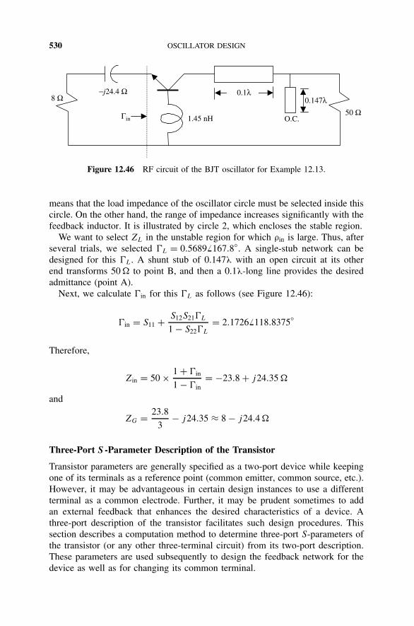
530 OSCILLATOR DESIGN
50 Ω0.147λ 8 Ω
0.1λ−j24.4 Ω
Γin 1.45 nH O.C.
Figure 12.46 RF circuit of the BJT oscillator for Example 12.13.
means that the load impedance of the oscillator circle must be selected inside thiscircle. On the other hand, the range of impedance increases significantly with thefeedback inductor. It is illustrated by circle 2, which encloses the stable region.
We want to select ZL in the unstable region for which ρin is large. Thus, afterseveral trials, we selected L = 0.5689 167.8. A single-stub network can bedesigned for this L. A shunt stub of 0.147λ with an open circuit at its otherend transforms 50 to point B, and then a 0.1λ-long line provides the desiredadmittance (point A).
Next, we calculate in for this L as follows (see Figure 12.46):
in = S11 + S12S21L
1 − S22L
= 2.1726 118.8375
Therefore,
Zin = 50 × 1 + in
1 − in= −23.8 + j24.35
and
ZG = 23.8
3− j24.35 ≈ 8 − j24.4
Three-Port S -Parameter Description of the Transistor
Transistor parameters are generally specified as a two-port device while keepingone of its terminals as a reference point (common emitter, common source, etc.).However, it may be advantageous in certain design instances to use a differentterminal as a common electrode. Further, it may be prudent sometimes to addan external feedback that enhances the desired characteristics of a device. Athree-port description of the transistor facilitates such design procedures. Thissection describes a computation method to determine three-port S-parameters ofthe transistor (or any other three-terminal circuit) from its two-port description.These parameters are used subsequently to design the feedback network for thedevice as well as for changing its common terminal.

MICROWAVE TRANSISTOR OSCILLATORS 531
Port 1 Port 2
Port 3
Figure 12.47 Three-port network.
Consider a three-port network as illustrated in Figure 12.47. Incident andreflected waves at the three ports are related through its S-parameters as follows.
b′1
b′2
b′3
=
S ′
11 S ′12 S ′
13S ′
21 S ′22 S ′
23S ′
31 S ′32 S ′
33
a′
1a′
2a′
3
(12.7.6)
It can be shown that these S-parameters satisfy the following two conditions, andtherefore all nine elements of the scattering matrix are not independent:
3∑i=1
S ′ij = 1 j = 1, 2, 3 (12.7.7)
and3∑
j=1
S ′ij = 1 i = 1, 2, 3 (12.7.8)
Condition (12.7.7) can be proved when there is negligible stray capacitance ateach port. In that case, the algebraic sum of the currents entering these portsmust be zero. Hence,
3∑n=1
in = 0
Using (8.6.15) and (8.6.16), we can write
3∑i=1
(a′i − b′
i ) = 0
or
3∑i=1
a′
i −3∑
j=1
S ′ij a
′j
= 0 (12.7.9)
If we select a′2 = a′
3 = 0, (12.7.9) simplifies to
a′1 −
∑S ′
i1a′1 = 0

532 OSCILLATOR DESIGN
or3∑
i=1
S ′i1 = 0 (12.7.10)
Similarly, for a′1 = a′
3 = 0,
3∑i=1
S ′i2 = 0 (12.7.11)
and for a′1 = a′
2 = 0,
3∑i=1
S ′i3 = 0 (12.7.12)
Hence, condition (12.7.7) is verified.The condition (12.7.8) can be verified as follows. When every port has the
same voltage there will be no input current provided that the stray capacitancefrom each terminal to ground is zero. Since ii = ai − bi , b′
i must be equal to a′i .
Consequently, b1 = b2 = b3 = a′ for a1 = a2 = a3 = a′. Hence,
b′i =
3∑j=1
S ′ij a
′j = a′
3∑j=1
S ′ij = a′ i = 1, 2, 3
or3∑
j=1
S ′ij = 1 i = 1, 2, 3
That proves condition (12.7.8).Using (8.6.15) and (8.6.16), we find that the normalized voltage at port 3 is
V3 = a′3 + b′
3. Let us now define new voltage waves at ports 1 and 2 as follows:
a1 = a′1 − V3
2= a′
1 − a′3 + b′
3
2(12.7.13)
b1 = b′1 − V3
2= b′
1 − a′3 + b′
3
2(12.7.14)
a2 = a′2 − V3
2= a′
2 − a′3 + b′
3
2(12.7.15)
and
b2 = b′2 − V3
2= b′
2 − a′3 + b′
3
2(12.7.16)

MICROWAVE TRANSISTOR OSCILLATORS 533
The new total voltages at ports 1 and 2 are now
V1 = a1 + b1 = a′1 + b′
1 − V3 (12.7.17)
and
V2 = a2 + b2 = a′2 + b′
2 − V3 (12.7.18)
Thus, these voltages are referred to the port 3 voltage.Note that these definitions of new incident and reflected waves do not change
the port currents; that is,
b1 − a1 = b′1 − a′
1 (12.7.19)
and
b2 − a2 = b′2 − a′
2 (12.7.20)
The two-port scattering matrix that relates b1 and b2 to a1 and a2 will now makethe port 3 terminal common. Hence,
b1 = S11a1 + S12a2 (12.7.21a)
b2 = S21a1 + S22a2 (12.7.21b)
Combining (12.7.13) to (12.7.21), we have
b′1 − a′
3 + b′3
2= S11
(a′
1 − a′3 + b′
3
2
)+ S12
(a′
2 − a′3 + b′
3
2
)(12.7.22a)
and
b′2 − a′
3 + b′3
2= S21
(a′
1 − a′3 + b′
3
2
)+ S22
(a′
2 − a′3 + b′
3
2
)(12.7.22b)
From Kirchhoff’s current law, the sum of all currents flowing into the threeterminals must be zero. Therefore, we can write
a′1 − b′
1 + a′2 − b′
2 + a′3 − b′
3 = 0 (12.7.23)
Rearranging (12.7.22) and (12.7.23), we get
b′1 = S11a
′1 + S12a
′2 + (1 − S11 − S12)
a′3 + b′
3
2(12.7.24a)
b′2 = S21a
′1 + S22a
′2 + (1 − S21 − S22)
a′3 + b′
3
2(12.7.24b)

534 OSCILLATOR DESIGN
andb′
3 = a′1 + a′
2 + a′3 − b′
1 − b′2
= a′1 + a′
2 + a′3 − S11a
′1 − S12a
′2 − (1 − S11 − S12)
a′3 + b′
3
2
− S21a′1 − S22a
′2 − (1 − S21 − S22)
a′3 + b′
3
2
or
b′3 = 212
4 − a′
1 + 221
4 − a′
2 +
4 − a′
3 (12.7.25)
where
12 = 1 − S11 − S21 (12.7.26a)
21 = 1 − S12 − S22 (12.7.26b)
= S11 + S22 + S12 + S21 = 2 − 12 − 21 = 2 − 11 − 22 (12.7.26c)
11 = 1 − S11 − S12 (12.7.26.d)
22 = 1 − S21 − S22 (12.7.26.e)
Now from (12.7.24) and (12.7.25), we find that
b′1 =
(S11 + 1112
4 −
)a′
1 +(
S12 + 1121
4 −
)a′
2 + 211
4 − a′
3 (12.7.27a)
b′2 =
(S21 + 2212
4 −
)a′
1 +(
S22 + 2221
4 −
)a′
2 + 222
4 − a′
3 (12.7.27b)
Equations (12.7.25) and (12.7.27) can be expressed in matrix form as
b′1
b′2
b′3
=
S11 + 1112
4 − S12 + 1121
4 −
211
4 −
S21 + 2212
4 − S22 + 2221
4 −
222
4 −
212
4 −
221
4 −
4 −
a′1
a′2
a′3
(12.7.28)
Therefore, if two-port S-parameters of a three-terminal device are given withterminal 3 common, the corresponding three-port scattering matrix can be foundfrom (12.7.28). If we are given the scattering matrix of a transistor in its common-emitter configuration, it can be converted to a three-port device (four-terminaldevice) where the fourth terminal is a common ground point and its nine scatteringparameters can be found via (12.7.28).

MICROWAVE TRANSISTOR OSCILLATORS 535
Feedback Network Design Consideration
If a load impedance Z is connected between terminal 3 and the ground, thenb′
3 = a′3, where
= Z − Z0
Z + Z0
Therefore,
b′3 = a′
3 = S ′31a
′1 + S ′
32a′2 + S ′
33a′3
or
a′3 = − S ′
31
S ′33 − −1
a′1 − S ′
32
S ′33 − −1
a′2 (12.7.29)
Scattering parameters of the resulting two-port network can be found from (12.7.6)and (12.7.29) as follows:
b′1 =
(S ′
11 − S ′13S
′31
S ′33 − −1
)a′
1 +(
S ′12 − S ′
13S′32
S ′33 − −1
)a′
2 (12.7.30)
and
b′2 =
(S ′
21 − S ′23S
′31
S ′33 − −1
)a′
1 +(
S ′22 − S ′
23S′32
S ′33 − −1
)a′
2 (12.7.31)
These two equations can be expressed in matrix form as follows and the corre-sponding new Sijn can be identified:
[b′
1
b′2
]=
(S ′
11 − S ′13S
′31
S ′33 − −1
) (S ′
12 − S ′13S
′32
S ′33 − −1
)(
S ′21 − S ′
23S′31
S ′33 − −1
) (S ′
22 − S ′23S
′32
S ′33 − −1
)
[a′
1
a′2
]
=[
S11n S12n
S21n S22n
][a′
1
a′2
](12.7.32)
If port 3 is grounded (i.e., V3 = 0), in (12.7.32) is −1.A similar procedure may be adopted for the other ports. In other words, if port
1 is terminated by impedance Z, b1 = a1. The S-parameters of this new two-port network that is formed by ports 2 and 3 of the original three-port networkcan be determined from (12.7.6). Suppose that the common-source S-parametersof a FET are given, whereas the design procedure requires its common-gate S-parameters; then the computation proceeds as follows. First, we determine itsthree-port S-parameters using (12.7.28). The source terminal forms the third port

536 OSCILLATOR DESIGN
of the FET while its gate and drain terminals remain as ports 1 and 2 of the three-port network. Next, we switch back to a two-port network by short-circuiting port1. If a feedback network is needed, that impedance is used to terminate this port.
As (12.7.32) indicates, the S-parameters of the new two-port network can bemodified to a certain extent by adjusting the terminating impedance Z. Note thatits reflection coefficient will satisfy the equations
= S11n − S ′11
S11nS′33 − 1
(12.7.33)
and
= S22n − S ′22
S22nS′33 − 2
(12.7.34)
where
1 = S ′11S
′33 − S ′
31S′13 (12.7.35)
and
2 = S ′22S
′33 − S ′
32S′23 (12.7.36)
In the case of a reactive termination at port 3, || = 1. It maps a circle in theS11n-plane, the center C1 and radius R1 of which are given as
C1 = S ′11 − 1S
′∗33
1 − |S ′33|2
(12.7.37)
and
R1 = |S ′31S
′13|
|1 − |S ′33|2|
(12.7.38)
Similarly, center C2 and radius R2 of the circle for S22n are found as follows:
C2 = S ′22 − 2S
′∗33
1 − |S ′33|2
(12.7.39)
and
R2 = |S ′32S
′23|
|1 − |S ′33|2|
(12.7.40)
These circles are drawn on a Smith chart and S11n and S22n are optimizedfor the desired feedback. In the case of an oscillator design, a positive feedbackis desired. In other words, the inverse of the conditions (11.1.16) and (11.1.18)must hold so that the transistor becomes potentially unstable. Alternatively, theµ-factor can be determined from the following equation, and its magnitude shouldbe kept to a small value that is less than unity. (Les Besser, Applied Microwave

MICROWAVE TRANSISTOR OSCILLATORS 537
and Wireless, pp. 44–55, Spring 1995). The transistor is unconditionally stablefor magnitudes greater than unity.
µ = 1 − |S22n|2|S11n − nS
∗22n| + |S21nS12n| (12.7.41)
wheren = S11nS22n − S12nS21n (12.7.42)
Example 12.14 Reconsider the BJT of Example 12.13. Find its three-port S-parameter description. Use the inductive termination at its base and verify whetherthat provides optimum feedback for the oscillator design.
SOLUTION From (12.7.28), the three-port S-parameters are found as follows:
S ′
11 S ′12 S ′
13S ′
21 S ′22 S ′
23S ′
31 S ′32 S ′
33
=
0.396 84.4 0.393 29.3 0.852 − 43.5
0.582 − 79.1 0.534 − 54.7 1.163 60
0.87 11.8 0.425 34.9 0.466 − 115.4
The reactance of a 1.45-nH inductor is j25.0542 and its reflection coefficient can be found easily for Z0 = 50 . The S-parameters of the resulting two-port
1.
R2
R1
C2
C1
+j0.5
+j0.5
0.5
0.25
00
−0.25
−1.
0.33
−0.5
1. 5.
−2.
2.
Figure 12.48 S11n and S22n circles on a Smith chart.

538 OSCILLATOR DESIGN
network are found from (12.7.32) as[S11n S12n
S21n S22n
]=
[1.722 100.1 0.714 94.8
2.083 − 136.4 1.163 − 102.5]
These results are very close to those obtained in Example 12.13. Minor deviationsare attributed to the roundoff errors involved.
To verify the feedback provided by the inductor, we first plot S11n and S22n
circles on a Smith chart. To that end, the information of these circles is foundfrom (12.7.37) to (12.7.40). The results are C1 = 0.837 84, R1 = 0.947, C2 =0.587 − 84.6, and R2 = 0.631. These two circles are illustrated in Figure 12.48.It may easily be verified that the points indicated on these circles correspond toS11n and S22n of the two-port network obtained with an inductive termination ofj0.5 at the base terminal. Further, the magnitude of the µ-factor of the transistor(without feedback inductor) in common-base configuration is 0.674. It means thatthe transistor is potentially unstable. When the inductor is added to its base, themagnitude of the µ-factor decreases to 0.126. Hence, the inductor enhances thepositive feedback further to facilitate the oscillator design.
SUGGESTED READING
Bahl, I. J., and Bhartia, P., Microwave Solid State Circuit Design. New York: Wiley, 1988.
Collin, R. E., Foundations for Microwave Engineering. New York: McGraw-Hill, 1992.
Davis, W. A., Microwave Semiconductor Circuit Design. New York: Van Nostrand Rein-hold, 1984.
Gonzalez, G., Microwave Transistor Amplifiers. Upper Saddle River, NJ: Prentice Hall,1997.
Larson, L. E. (ed.), RF and Microwave Circuit Design for Wireless Communications.Boston: Artech House, 1996.
Pozar, D. M., Microwave Engineering. New York: Wiley, 1998.Rohde, U. L., Microwave and Wireless Synthesizers. New York: Wiley, 1997.
Smith, J. R., Modern Communication Circuits. New York: McGraw-Hill, 1998.
Vendelin, G. D., Pavio, A., and Rhode, U. L., Microwave Circuit Design Using Linearand Non-linear Techniques. New York: Wiley, 1990.
PROBLEMS
12.1. In Figure P12.1, the gain of the amplifier is constant with frequency [i.e.,Av(jω) = A0] and
β(jω) = 10−6
1 − j (ω − 2π × 109)
Use the Barkhausen criteria to determine the frequency of oscillation andthe required value of Ao.

PROBLEMS 539
Σ
Av(jω)
β(jω)
VoVi
Figure P12.1
12.2. In Figure P12.2, the gain of the amplifier [Av(jω)] and the feedbackfactor β(jω) are given as follows:
Av(jω) = − 8.45
1 + j (8 ω × 10−10)
and
β(jω) = 1
(1 + j5 ω × 10−10)2
Av(jω)
β(jω)
Vo
Figure P12.2
Determine the frequency of oscillation if the circuit oscillates.
12.3. (a) In the circuit shown in Figure P12.3, should the gain of the amplifierbe positive or negative to create the possibility for it to oscillate?
10 kΩ
10 kΩ
C
C
A
Figure P12.3
(b) What value should |A| have to cause sinusoidal oscillations?
(c) Find the capacitance C for the oscillations to occur at 10 kHz.

540 OSCILLATOR DESIGN
12.4. Complete the design of the biased BJT Colpitts oscillator circuit shownin Figure P12.4 for it to oscillate at 150 MHz.
15 V
RFC
L3
CB2CB1
C2
C110 kΩ 1 kΩ
50 kΩ
Figure P12.4
12.5. In the circuit shown in Figure P12.5, the FET is biased such that its gm is4.5 mS. For this circuit to oscillate at 100 MHz, find C1 and C2. An open-loop gain of 5 ensures the beginning of oscillations, and the unloaded Q
value of a 100-nH inductor is 1000.
C1
C2 100 nH
VDD1 kΩ
Figure P12.5
12.6. In the circuit shown in Figure P12.6 the FET is biased such that its gm
is 4.5 mS. For this circuit to oscillate at 100 MHz, find L1 and L2. Anopen-loop gain of 5 ensures the beginning of oscillations.
L1
L2 1 pF
VDD
1 kΩ
100 nF
Figure P12.6
12.7. Free-running frequency and the gain factor of a voltage-controlled oscil-lator are given as 500 MHz and 150 kHz/V, respectively. It is being used

PROBLEMS 541
in a PLL along with a sinusoidal phase detector with maximum output of5 V at θe = π/2 radians. If there are no amplifiers or frequency dividerin the loop, what is its hold-in range?
12.8. If the phase detector in Problem 12.7 is replaced by a triangular type withVe max = A = 5 V at θe max = π/2 radians, find the new holding range.
12.9. In the PLL shown in Figure P12.9, peak amplitudes of the reference inputas well as the VCO output are 1.5 V. An analog multiplier is being usedas the phase detector that has 5 V output when its reference input, Vin,and the oscillator signal, Vosc, both are 2 V. The free-running frequencyof the VCO is 50 MHz, which reduces to zero when its control voltageVcntl is reduced by 5 V. Find the phase difference between the input andthe VCO output when it is in lock with input frequency of (a) 55 MHzand (b) 45 MHz.
PD F(s) VCO
Vosc
Vin
VPD Vd
Figure P12.9
12.10. Analyze the PLL system shown in Figure P12.10. By controlling thefrequency divider, its output frequency can be changed from 4 MHz to6 MHz in steps of 200 kHz. The transfer function of the phase detector,Kd , is 0.5 V/rad. The free-running frequency and gain factor of VCO are5 MHz and 107 rad/s·V, respectively. The voltage gain of the amplifier is20. Design a passive lead–lag low-pass filter that can be used in the loop.
frfoPhase detector
Low-passfilter
Voltage-controlledoscillator
AmplifierKa = 20
Frequencydivider
1N
VdVe
θe = θo/N θo
Figure P12.10
12.11. Design a multiple phase-locked-loop synthesizer to cover the frequencyrange 100.0 to 200.0 MHz in 100-Hz increments. The loop frequencyswitching time should not exceed 25 ms.

542 OSCILLATOR DESIGN
12.12. Design a multiple phase-locked-loop synthesizer to cover the frequencyrange 35.40 to 40.0 MHz in 10-Hz increments. The reference frequencyis to be 100 kHz. No loop should operate with a reference frequencybelow 100 kHz.
12.13. Design a three-loop synthesizer to cover the frequency range 190 to200 MHz in steps of 10 Hz. The loop frequency switching time shouldnot exceed 25 ms.
12.14. A 2-GHz oscillator is to be designed using a negative resistance diode withits reflection coefficient G as 2.05 − 60 (measured with Z0 = 50
as reference). Determine its load impedance.
12.15. The S-parameters of a GaAs MESFET are measured in the common-source mode at Vds = 6 V and Ids = 50 mA at 8 GHz. The resultsare found as follows. S11 = 0.63 − 150, S12 = 0.07 − 30, S21 =3.10 40, and S22 = 0.70 − 100. Determine its S-parameters incommon-gate configuration.
12.16. A silicon BJT is biased at VCE = 18 V and IC = 30 mA. Its S-parametersmeasured at 5.0 GHz in the common-emitter configuration are found tobe S11 = 0.63 − 150, S12 = 0.007 30, S21 = 2.10 40, and S22 =0.70 − 100. Find its S-parameters in common-base configuration.
12.17. A silicon BJT is biased at VCE = 10 V and IC = 40 mA. Its S-parametersmeasured at 8.0 GHz in the common-base configuration are found tobe S11 = 1.32 88, S12 = 0.595 99, S21 = 1.47 172, and S22 =1.03 − 96. Find its S-parameters in common-emitter configuration.
12.18. Design an oscillator to operate at 8 GHz using the common-gate config-uration of MESFET given in Problem 12.15. Use an inductor at its gateterminal to provide positive feedback, if necessary. Determine the valueof the feedback inductor.
12.19. Design an oscillator to operate at 5 GHz using the common-base con-figuration of BJT given in Problem 12.16. Use an inductor at its baseterminal to provide positive feedback, if necessary. Determine the valueof the feedback inductor.

13DETECTORS AND MIXERS
Detector and mixer circuits employ nonlinear electronic devices to process elec-trical information. For example, if a transmission line is being used to send onlyone voice signal at a given time, it can be connected directly without a problem.On the other hand, if two different voice signals are sent over this line at thesame time, no information can be retrieved at the other end due to their interfer-ence. In practice, for economic reasons, a large number of telephone subscribersmay need to be connected via a single long-distance communication line. Thisrequires some means to move each voice channel to a different frequency band.This solution is frequency-division multiplexing (FDM). A commonly used FDMhierarchy is illustrated in Figure 13.1. Such multiplexing systems require mixersand detectors.
Similarly, wireless systems operate at higher frequencies to achieve efficientand directional radiation from an antenna. In this case, electrical informationis generally superimposed on a high-frequency carrier signal via amplitude orfrequency modulation. In amplitude modulation (AM), the amplitude of a radio-frequency signal (the carrier) varies according to the information (the modulating)signal. In the case of frequency modulation (FM), the frequency of carrier signalvaries according to the modulating signal. Figure 13.2 illustrates various wave-forms associated with these modulations.
The chapter begins with an overview of the characteristics of these modulationsand their detection schemes. Several mixer circuits are then presented that canbe designed using diodes or transistors as nonlinear electronic devices.
Radio-Frequency and Microwave Communication Circuits: Analysis and Design, Second Edition,By Devendra K. MisraISBN 0-471-47873-3 Copyright 2004 John Wiley & Sons, Inc.
543

544 DETECTORS AND MIXERS
3054 kHz
2814 kHz
2574 kHz
1134 kHz
1374 kHz
894 kHz
108 kHz
552 kHz
504 kHz
456 kHz
408 kHz
360 kHz
12 C
hann
els
(eac
h w
ith 0
−4 k
Hz
band
wid
th)
5 B
asic
gro
ups
10 S
uper
gro
ups
Basic group60−108 kHz
Super group312−552 kHz
Master group654−3054 kHz
104 kHz
72 kHz
68 kHz
64 kHz
100 kHz
Figure 13.1 FDM hierarchy.
13.1 AMPLITUDE MODULATION
Consider the AM system illustrated in Figure 13.3. Assume that two inputs tothis circuit are s(t) = a0 + b0m(t) and c(t) = cos(ωct + ψ). The output signalcAM(t) is then found as
cAM(t) = s(t)c(t) = a0
[1 + b0
a0m(t)
]cos(ωct + ψ) (13.1.1)
An analysis of this expression shows that cAM(t) represents an amplitude-modu-lated signal with s(t) as the modulating signal and c(t) as the carrier. Further,the ratio b0/a0 is called the modulation index.
If the modulating signal is m(t) = cos ωmt , (13.1.1) can be simplified as follows:
cAM(t) = a0
(1 + b0
a0cos ωmt
)cos(ωct + ψ)
or
cAM(t) = a0 cos(ωct + ψ) + b0
2cos[(ωc + ωm)t + ψ] + cos(ωc − ωm)t + ψ
(13.1.2)This can easily be graphed to verify that indeed it represents an AM signalas illustrated in Figure 13.2. Further, it shows that the output has three sinu-soidal signals, each with different frequencies. Its frequency spectrum is shownin Figure 13.4. Besides the carrier frequency ωc, there are two other frequen-cies as ωc ± ωm. The signal spectrum ωc + ωm represents the upper sideband;
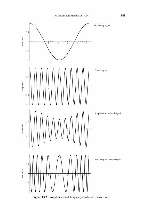
AMPLITUDE MODULATION 545
1 2 3 4 5 6
1 2 3 4 5 6
−1
−0.5
0.5
−1
−0.5
0.5
1
Am
plitu
de
Am
plitu
de
Carrier signal
t
t
Modulating signal
1 2 3 4 5 6
1 2 3 4 5 6
−1
−0.5
0.5
1
1
−1
−0.5
0.5
Amplitude-modulated signal
Frequency-modulated signal
Am
plitu
de
Am
plitu
de
t
t
Figure 13.2 Amplitude- and frequency-modulated waveforms.

546 DETECTORS AND MIXERS
CAM(t) s(t)
c(t)
AMcircuit
Figure 13.3 Amplitude-modulation system.
ωc − ωm ωc + ωmωcω
Figure 13.4 Frequency spectrum of cAM(t).
ωc − ωm is the lower sideband. Note that each sideband includes the informa-tion signal ωm. When only one of these signals is used to send the information,it is called single-sideband (SSB) AM transmission. On the other hand, com-plete cAM(t) represents double-sideband (DSB) AM transmission. It is calledsuppressed carrier AM if the carrier component of cAM(t) is filtered out beforetransmitting.
Example 13.1 A 100-MHz sinusoidal signal is being used as the carrier forAM transmission. Its amplitude is 1000 V and the average power is 10 kW.The modulating signal is s(t) = 3 cos ω1t + 2 cos 2 ω1t + cos 3 ω1t , where ω1 =4π × 106 rad/s. The modulation index is 0.15.
(a) Determine the frequency spectrum of the signal modulated. Find the ampli-tude of each sinusoidal component, the power in the carrier and each pair ofsidebands, and the total bandwidth of the AM signal.
(b) Determine the peak amplitude and peak instantaneous power of this signal.
SOLUTION Since amplitude of the carrier signal is 1000 V and its poweris 10 kW, the proportionality constant that relates the two can be determined.For P = αV 2,
α = P
V 2= 10,000
1,000,000= 0.01
The AM signal can be determined from (13.1.1) as follows:
CAM(t) = 1000[1 + 0.15(3 cos ω1t + 2 cos 2 ω1t + cos 3 ω1t)] cos ωct V
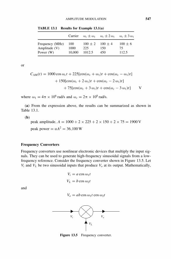
AMPLITUDE MODULATION 547
TABLE 13.1 Results for Example 13.1(a)
Carrier ωc ± ω1 ωc ± 2 ω1 ωc ± 3 ω1
Frequency (MHz) 100 100 ± 2 100 ± 4 100 ± 6Amplitude (V) 1000 225 150 75Power (W) 10,000 1012.5 450 112.5
or
CAM(t) = 1000 cos ωct + 225[cos(ωc + ω1)t + cos(ωc − ω1)t]
+ 150[cos(ωc + 2 ω1)t + cos(ωc − 2 ω1)t]
+ 75[cos(ωc + 3 ω1)t + cos(ωc − 3 ω1)t] V
where ω1 = 4π × 106 rad/s and ωc = 2π × 108 rad/s.
(a) From the expression above, the results can be summarized as shown inTable 13.1.
(b)peak amplitude, A = 1000 + 2 × 225 + 2 × 150 + 2 × 75 = 1900 V
peak power = αA2 = 36,100 W
Frequency Converters
Frequency converters use nonlinear electronic devices that multiply the input sig-nals. They can be used to generate high-frequency sinusoidal signals from a low-frequency reference. Consider the frequency converter shown in Figure 13.5. LetVi and VL be two sinusoidal inputs that produce Vo at its output. Mathematically,
Vi = a cos ω1t
VL = b cos ω2t
and
Vo = ab cos ω1t cos ω2t
Vi Vo
VL
Figure 13.5 Frequency converter.

548 DETECTORS AND MIXERS
Vi Vo
VL
BPF ω1 + ω2
Figure 13.6 Up-converter circuit.
Vi Vo
VL
BPF ω1 − ω2
Figure 13.7 Down-converter circuit.
Output Vo can be rearranged as follows:
Vo = ab
2cos[(ω1 + ω2)t] + cos[(ω1 − ω2)t] (13.1.3)
Hence, the output is a sum of two sinusoidal signals. These sum and differencefrequency signals can be filtered out for up or down conversions as illustrated inFigures 13.6 and 13.7, respectively.
Single-Diode Mixer Circuit Arrangement
Consider the circuit arrangement shown in Figure 13.8. Two inputs, vs and vL,are added together before applying to a diode. Capacitors C1 and C2 are usedto block the dc bias of the diode from other sides of the circuit. Thus, thesecapacitors are selected such that there is negligible reactance for the ac signal.Similarly, inductors L1 and L2 are used to block ac from short-circuiting via thedc source. Hence, these inductors should have very high reactance at ac, whereasdc passes through with negligible loss. Thus, the voltage applied to the diode hasboth ac and dc components.
To analyze this circuit and determine its output signal, we need to consider theactual characteristics of the diode. The V –I characteristic of a typical forward-biased diode is illustrated in Figure 13.9. For the present case, bias voltage Vb
is assumed high enough to keep the diode forward biased. If the current throughthis diode is id and the voltage across its terminals is vd ,
id = Is(eαvd − 1) (13.1.4)

AMPLITUDE MODULATION 549
Matchingcircuit
+Vb
BPF vs
vL
C1 C2
L2
L1
Figure 13.8 Single-diode mixer circuit.
mA
−0.00005
−0.20 −0.15 −0.10 −0.05 0.00
V
0.05 0.10 0.15 0.200.00000
0.00005
0.00010
0.00015
0.00020
Figure 13.9 V –I characteristic of a typical diode.
whereα = q
nkT(13.1.5)
Is is called the reverse-saturation current (on the order of 10−8 to 10−15 A), q isthe electronic charge (1.602 × 10⁻¹⁹ C), n is a number ranging between 1 and 2, k
is the Boltzmann constant (1.38 × 10⁻²³ J/K), and T is the temperature in kelvin.Since the diode has both alternating and direct voltage across it, we can write
vd = Vb + vac
where vac = vs + vL. Therefore, current through the diode can be expressed as
id = Is(eα(Vb+vac) − 1) = Is(e
αVbeαvac − 1)

550 DETECTORS AND MIXERS
If vac Vb such that αvac is a small fraction, id can be expanded as follows.Further, it can be approximated only by a few terms of the series:
id = Is
eαVb
[1 + αvac + (αvac)
2
2+ · · ·
]− 1
After rearranging, we find that
id = Is(eαVb − 1) + Ise
αVb
[αvac + (αvac)
2
2+ · · ·
]= Ib + iac
Thus, there are two components in the diode current: a dc (Ib) and an ac (iac).The ac component iac through the diode may be approximated as
iac ≈ IseαVb
[αvac + (αvac)
2
2
]= gdvac + g′
d
v2ac
2(13.1.6)
where
gd = αIseαVb = α(Ib + Is) (13.1.7)
and
g′d = αgd (13.1.8)
Parameter gd is known as the dynamic conductance of the diode. It is equal tothe inverse of the junction resistance. Parameter g′
d has units of A/V2. A small-signal equivalent circuit of the diode can be drawn as shown in Figure 13.10. Itsjunction capacitance Cj appears in parallel with the junction resistance Rj . Thelead inductance Lp and bulk resistance Rs appear in series with this combination.As illustrated, packaging capacitance Cp between the two leads appears in parallelwith the circuit.
Cp
Cj Rj
Lp
Rs
Figure 13.10 Small-signal equivalent circuit of the diode.

AMPLITUDE MODULATION 551
Example 13.2 The equivalent-circuit parameters of a diode in an axial leadpackage are given as follows: Cp = 0.1 pF, Lp = 2.0 nH, Cj = 0.15 pF, Rs =10 , and Is = 10−8 A. Determine its junction resistance if the bias current is(a) zero and (b) 100 µA. Assume that the diode is at room temperature (T =290 K) and n = 1.
SOLUTION From (13.1.7),
Rj = 1
gd
= 1
α(Ib + Is)
andkT
q= 1.38 × 10−23 × 290
1.602 × 10−19= 0.025 V
(a)
Rj = 0.025
10−8 = 2500 k
(b)
Rj = 0.025
(100 + 0.01) × 10−6 = 249.9
Radio-Frequency Detector
Diodes are used for the detection of radio-frequency signals, to convert a partof RF input to dc. They are used for monitoring the power (relative powermeasurement), automatic gain control circuits, and the detection of AM signals.Assume that the RF signal, a1 cos ωt , is applied to a diode biased at Vb. Hence,the total voltage Vt applied to it is
Vt = Vb + a1 cos ωt
The corresponding diode current id can be expressed as follows:
id ≈ Ib + gda1 cos ωt + g′d
2a2
1 cos2 ωt
or
id ≈ Ib + g′d
a21
4+ gda1 cos ωt + g′
d
4a2
1 cos 2 ωt (13.1.9)
The current sensitivity, βi , of the diode is defined as a ratio of the change inoutput dc to that of RF input power. Hence,
βi = g′da
21/4
gda21/2
= g′d
2gd
(13.1.10)
The current sensitivity has units of A/W or V−1.

552 DETECTORS AND MIXERS
VoVin R C
Figure 13.11 Zero-biased diode detector circuit.
An open-circuit voltage sensitivity βv of the diode is defined as the ratio ofchange in direct voltage across the junction to that of RF input power. Hence,
βv = g′d
2g2d
= βiRj (13.1.11)
Voltage sensitivity has units of V/W or A−1. Its typical range is 400 to 1500 mA−1.Consider a diode circuit that has no dc bias voltage, as shown in Figure 13.11. Ifan amplitude-modulated signal Vin is applied to this circuit, current through thediode can be found through (13.1.6).
For Vin = Vo(1 + m cos ωmt) cos ωct
iac ≈ gdVo(1 + m cos ωmt) cos ωct + g′dV
2o
2(1 + m cos ωmt)2 cos2 ωct
or
iac ≈ gdVo
cos ωct + m
2cos[(ωm + ωc)t] + m
2cos[(ωm − ωc)t]
+ g′dV
2o
4
1 + m2
2+ 2m cos ωmt + m2
2cos 2 ωmt
+ cos 2 ωct + m cos[(2 ωc + ωm)t]
+ m cos[(2 ωc − ωm)t] + m2
2cos 2 ωct + m2
4cos[2(ωc + ωm)t]
+ m2
4cos[2(ωc − ωm)t]
(13.1.12)
Hence, the diode current has several frequency components, shown graphically inFigure 13.12. It includes the modulating signal frequency ωm. If this current flows
0
ωm
2ωm
ωc
− ω
m
2ωc
− 2ω
m
2ωc
+ 2ω
m
2ωc
− ω
m
2ωc
+ ω
m
2ωc
ωc
+ ω
mωc
Figure 13.12 Spectrum of the diode current given by (13.1.12).

AMPLITUDE MODULATION 553
through a resistance R, the corresponding voltage contains the same spectrumas well. A low-pass filter can be used to suppress the undesired high-frequencysignals. Note that there is a second harmonic 2 ωm of the modulating signalthat may sometimes be difficult to suppress. However, it may have relativelynegligible amplitude, especially when the modulation index m is less than unity.
As a special case, if an unmodulated radio-frequency signal is applied to thiscircuit, m is zero in (13.1.12). Therefore, the expression for the diode currentsimplifies to
iac ≈ g′dV
2o
4+ gdVo cos ωct + g′
dV2o m2
4cos 2 ωct
Therefore, a capacitor C connected across the output can easily suppress itssinusoidal components, while its first term represents a direct voltage that isproportional to the square of the RF amplitude Vo. This type of circuit is used inpractice to monitor radio frequency and microwave signals.
Coherent Detection of AM
An alternative technique for detection of amplitude-modulated signals is illus-trated in Figure 13.13. In this case, the amplitude-modulated signal is multi-plied with a sinusoidal signal that has the same frequency as the carrier signal.Assume that
CAM(t) = ao[1 + m(t)] cos(ωct + ϕ)
The voltage v(t) at the output of the multiplier is found to be
v(t) = CAM(t)a cos(ωct + ϕ) = aao[1 + m(t)] cos(ωct + ϕ) cos(ωct + ϕ)
or
v(t) = aao
2[1 + m(t)][cos(θ − ϕ) + cos(2 ωct + θ + ϕ)]
If the low-pass filter has a cutoff frequency below 2 ωc, its output voltage vo is
vo(t) = aao
2[1 + m(t)] cos(θ − ϕ)
Hence, this circuit can provide a more efficient way to extract the informationsignal from the AM than the one considered earlier. However, the output voltage
a cos(ωct + θ)
CAM(t) v(t)LPF vo(t)
Figure 13.13 Simple coherent detector circuit.

554 DETECTORS AND MIXERS
goes to zero if the argument of the cosine function (θ − ϕ) is 0.5π (90). Toensure maximum output voltage, this phase difference should be zero. In otherwords, the local oscillator signal should be phase locked to the carrier. This canbe done using the PLL scheme discussed in Chapter 12. This circuit arrangementis illustrated in Figure 13.14.
Single-Sideband Generation
As illustrated in Figure 13.4, the modulating signal is included in both of thesidebands of an AM signal. The precious frequency spectrum can be econo-mized if only one of these is used to transmit the information. For example, theFDM hierarchy shown in Figure 13.1 employs only the lower sideband. It can beachieved with a low-pass filter that passes only the desired component. On theother hand, it can be done more efficiently using the circuit in Figure 13.15. This
LPF vo(t)
LPF VCO
In-phasedetector
−90°phase shift
CAM(t)
Quadraturedetector
Figure 13.14 PLL-based coherent detection scheme.
90°, 3-dBdivider
B cos ωct
B sin ωct
A sin ωmt
A cos ωmt
AB cos(ωc − ωm)t
AB sin ωct sin ωmt
AB cos ωct cos ωmt
CarrierModulatingsignal
+
−
90°, 3-dBdivider
Figure 13.15 SSB generation scheme.
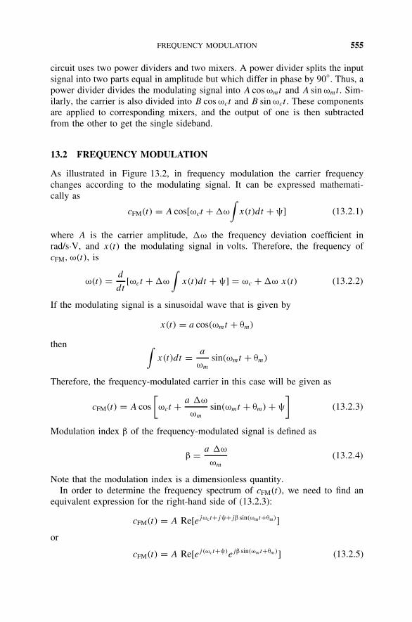
FREQUENCY MODULATION 555
circuit uses two power dividers and two mixers. A power divider splits the inputsignal into two parts equal in amplitude but which differ in phase by 90. Thus, apower divider divides the modulating signal into A cos ωmt and A sin ωmt . Sim-ilarly, the carrier is also divided into B cos ωct and B sin ωct . These componentsare applied to corresponding mixers, and the output of one is then subtractedfrom the other to get the single sideband.
13.2 FREQUENCY MODULATION
As illustrated in Figure 13.2, in frequency modulation the carrier frequencychanges according to the modulating signal. It can be expressed mathemati-cally as
cFM(t) = A cos[ωct + ω
∫x(t)dt + ψ] (13.2.1)
where A is the carrier amplitude, ω the frequency deviation coefficient inrad/s·V, and x(t) the modulating signal in volts. Therefore, the frequency ofcFM, ω(t), is
ω(t) = d
dt[ωct + ω
∫x(t)dt + ψ] = ωc + ω x(t) (13.2.2)
If the modulating signal is a sinusoidal wave that is given by
x(t) = a cos(ωmt + θm)
then ∫x(t)dt = a
ωm
sin(ωmt + θm)
Therefore, the frequency-modulated carrier in this case will be given as
cFM(t) = A cos
[ωct + a ω
ωm
sin(ωmt + θm) + ψ
](13.2.3)
Modulation index β of the frequency-modulated signal is defined as
β = a ω
ωm
(13.2.4)
Note that the modulation index is a dimensionless quantity.In order to determine the frequency spectrum of cFM(t), we need to find an
equivalent expression for the right-hand side of (13.2.3):
cFM(t) = A Re[ejωct+jψ+jβ sin(ωmt+θm)]
or
cFM(t) = A Re[ej(ωct+ψ)ejβ sin(ωmt+θm)] (13.2.5)

556 DETECTORS AND MIXERS
From the mathematical tables,
ejβ sin α =∞∑
n=−∞Jn(β)ejnα
where Jn(β) is the Bessel function of the first kind and order n. Therefore,
cFM(t) = A Re
[ ∞∑n=−∞
Jn(β)ej [ωc t+ψ+n(ωmt+θm)]
]
or
cFM(t) = A
∞∑n=−∞
Jn(β) cos[(ωc + nωm)t + nθm + ψ] (13.2.6)
whereJ−n(β) = (−1)nJn(β)
Therefore, the frequency spectrum of this FM signal extends to infinity asshown in Figure 13.16. As may be observed, the amplitudes of these harmonicsare going down for the higher-order terms. Since these amplitudes include theBessel function, a meaningful conclusion can be drawn only after understandingits characteristics. As illustrated in Figure 13.17, the magnitude of a Bessel func-tion is much smaller than unity if its order n is much larger than its argument β.In particular,
Jn(β) 1 for n β
Therefore, the infinite series of (13.2.6) can be terminated at finite n. The band-width Bc determined this way, known as the Carson rule bandwidth, takesn = β + 1 terms of the infinite series into account. It is given by
Bc = 2(β + 1)ωm rad/s (13.2.7)
If β is very large, Bc occupies a bandwidth β + 1 times larger than that whichwould be produced by an AM signal. It is known as wideband FM. On the other
ωc
− 3ω
m
ωc
− 2ω
m
ωc
− ω
m ωc
ωc
+ ω
m
ωc
+ 2ω
m
ωc
+ 3ω
m
AJ 3
(β) AJ 2
(β)
AJ 1
(β)
AJ 0
(β)
AJ 1
(β)
AJ 2
(β)
AJ 3
(β)
Figure 13.16 Spectrum of the FM signal with sinusoidal modulation.

FREQUENCY MODULATION 557
2 4 6 8 10
−0.4
-0.2
0.2
0.4
0.6
0.8
1
n = 0
n = 1
n = 2n = 3
β
Figure 13.17 Bessel function of the first kind for n = 0, 1, 2, and 3.
hand, if β is much smaller than unity, the FM bandwidth is comparable to thatof an AM system and is known as narrowband FM.
Example 13.3 A frequency modulator is connected with a carrier, fc = 5 MHz,and an audio signal Vm = 1 V of fm = 1 kHz. It produces frequency deviation of±10 kHz at the output of the modulator.
(a) An FM wave from the modulator is passed through a series of frequencymultipliers with a total multiplication factor of 12; that is, fo = 12fin. What isthe frequency deviation at the output?
(b) The output of the modulator (fc = 5 MHz, f = 10 kHz) is input to amixer stage along with a 55-MHz signal from an oscillator. Find the sum fre-quency output fo of the mixer and the frequency deviation fo.
(c) What is the modulation index at the output of the modulator?
(d) The audio input to the modulator is changed to Vm = 2 V and fm =500 Hz. At the modulator output, what will be the modulation index and fre-quency deviation f ?
SOLUTION The problem can be solved as follows:
(a) Since the input frequency is multiplied by a factor of 12, the frequencydeviation at the output of the multiplier will be ±10 kHz × 12 = ±120 kHz.

558 DETECTORS AND MIXERS
VL
VoVi
5 MHz ± 10 kHz
55 MHz
55 MHz ± (5 MHz ± 10 kHz)
Figure 13.18 Setup for Example 13.3.
(b) The arrangement is illustrated in Figure 13.18. Therefore, the sum fre-quency in the output is given as
55 MHz + 5 MHz + 10 kHz = 60.01 MHz
The frequency deviation is ± 5.01 MHz.
(c) From (13.2.4),
β = a ω
ωm
= a f
fm
= 1 × 10 kHz
1 kHz= 10
(d) The frequency deviation in this case increases by a factor of 2. Therefore,
β = a ω
ωm
= a f
fm
= 2 × 10 kHz
500 Hz= 40
FM Detector
A PLL is frequently employed for the detection of FM signals. Consider that thereference signal vr(t) in Figure 13.19 is an FM signal:
vr(t) = Ar sin[ωct + θr (t)]
where
θr (t) = ω
∫ t
m(τ) dτ
PD F(s)
vo(t)
v2(t)vr(t)
v1(t)
VCO
Figure 13.19 FM detection scheme using a PLL.

SWITCHING-TYPE MIXERS 559
In the transform domain it can be expressed as
θr (s) = ωM(s)
s
The transfer function of the system shown in Figure 13.19 is
V2(s)
θr (s)= KdF(s)
1 + Kd(Ko/s)F (s)= sKdF (s)
s + KdKoF (s)
Hence, the output voltage in the frequency domain is found to be
V2(s) = sKdF (s)
s + KdKoF (s)ω
M(s)
s= ω KdF(s)M(s)
s + KdKoF (s)
Assuming that M(s) has a bandwidth B and |F(s)| = 1 in the passband, thisexpression can be simplified as
V2(s) = ω KdM(s)
s + KdKo
= ω M(s)/Ko
1 + s/KdKo
≈ ω M(s)
Ko
Hence, for KdKo very large such that∣∣∣∣ s
KdKo
∣∣∣∣ 1
we have
V2(s) ≈ ωM(s)
Ko
Switching back to the time domain, we find that the output voltage will begiven as
v2(t) ≈ ω
Ko
m(t)
Hence, the output voltage v2(t) is proportional to the information signal m(t).
13.3 SWITCHING-TYPE MIXERS
It can easily be shown from (13.1.9) that the output of a single-diode mixercircuit contains both the local oscillator and RF input frequencies. Sometimes itmay be hard to filter these out from the desired signal. In this section we presentefficient ways to accomplish this. It is assumed for simplicity that the diodesused in these circuits are ideal. Hence, it turns the circuit on or off dependingon whether it is forward or reverse biased. Because of this characteristic, thesecircuits are termed switching-type mixers.

560 DETECTORS AND MIXERS
Switching-type mixers can be divided into two categories. In single-balancedmixers the local oscillator or the RF input can be balanced out such that it does notappear in the output. On the other hand, the output of a double-balanced mixercontains neither of the input frequencies. Consider the single-balanced mixercircuit shown in Figure 13.20. The transformer and diodes are assumed ideal forsimplicity. Further, it is assumed that the local oscillator voltage vL is a squarewave with a large amplitude compared with vi . Therefore, only the local oscillatorsignal determines the conduction through a given diode. An equivalent of thiscircuit is shown in Figure 13.21. When vL is positive, diode D1 is on and D2 isoff. The reverse is true if vL switches to its negative polarity. Mathematically,
vo =vL + vi vL > 0vL − vi vL < 0
or
vo = vL + v′i (13.3.1)
where
v′i = vis(t) (13.3.2)
s(t) =
1 vL > 0−1 vL < 0
(13.3.3)
+vG
−
+vi
−
+ +vi
vL
−
− − vo +
+vi−
RG
RL
D1
D2
Figure 13.20 Switching type single-balanced mixer.
+ +vivL
−− − vo +
+vi−
RL
D1
D2
Figure 13.21 Equivalent of the circuit shown in Figure 13.20.

SWITCHING-TYPE MIXERS 561
Hence, the switching frequency of s(t) is ωL, the same as the local oscilla-tor frequency.
Using Fourier series representation, s(t) may be expressed as follows:
s(t) = 4
π
∞∑n=1
(−1)n+1
nsin
nπ
2cos nωLt (13.3.4)
If vi is a sinusoidal signal,vi = V cos ωi t
then
v′i = 2V
π
∞∑n=1
(−1)n+1
nsin
nπ
2cos[(nωL + ωi )t] + cos[(nωL − ωi )t] (13.3.5)
Therefore, the output voltage can be expressed as
vo = vL + v′i = vL + 2V
π
∞∑n=1
(−1)n+1
nsin
nπ
2cos[(nωL + ωi )t]
+ cos[(nωL − ωi )t] (13.3.6)
Thus, output consists of the local oscillator frequency ωL and an infinite numberof sum and difference frequencies of ωi with odd multiples of ωL. Frequencycomponents ωL + ωi and ωL − ωi represent the upper and lower sidebands,respectively, each with amplitudes equal to 2V/π. These components can beseparated from the other higher-order terms, known as spurious signals.
Note that this formulation is based on the ideal switching characteristic ofthe diode. In other words, it assumes that the local oscillator switches the diodecurrent instantaneously. Deviation from this characteristic increases the distortionin its output. A major disadvantage of this mixer circuit is that the local oscillatorsignal appears in its output. Frequency components ωL and ωL ± ωi may be veryclose if the local oscillator frequency is high. In this situation, it may be difficultto separate the signals.
An alternative circuit that blocks the local oscillator signal from appearing atits output is depicted in Figure 13.22. As before, it can be analyzed easily byassuming that the diodes are ideal and that the local oscillator voltage controlsits switching. A simplified equivalent of this circuit is shown in Figure 13.23. Inthis circuit, both diodes conduct (on) when the local oscillator voltage is positiveand they do not conduct (off) otherwise. Hence, the output voltage vo can bewritten as
vo = vis(t) (13.3.7)

562 DETECTORS AND MIXERS
vo
+vG
−
+vi−
+ +vi
vL
−
−
+vi−
D1
D2
RL
RG
Figure 13.22 Another switching-type single-balanced mixer.
RL
vL
vo
−
+ vi−
+ + vi−
D1
D2
Figure 13.23 Equivalent of the single-balanced mixer shown in Figure 13.22.
where
s(t) =
1 vL > 00 vL < 0
(13.3.8)
This s(t) can be expressed in terms of the Fourier series as
s(t) = 1
2+
∞∑n=1
2
nπsin
nπ
2cos nωLt (13.3.9)
For vi = V cos ωi t , the output voltage is found to be
vo = V
2cos ωi t + V
π
∞∑n=1
1
nsin
nπ
2cos[(nωL + ωi )t] + cos[(nωL − ωi )t]
(13.3.10)
Thus, the output of this mixer circuit does not contain the local oscillator signal.However, it includes the input signal frequency ωi that appears with the sidebandsand spurious signals. It can be a problem in certain applications. For example,consider a case where the input and the local oscillator signal frequencies ata receiver are 60 and 90 MHz, respectively. As illustrated in Figure 13.24, thedifference signal frequency at its output is 30 MHz. If a 30-MHz signal is also
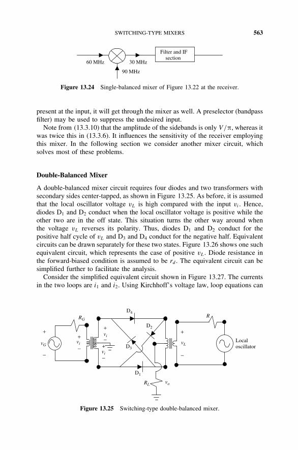
SWITCHING-TYPE MIXERS 563
90 MHz
60 MHz 30 MHz
Filter and IFsection
Figure 13.24 Single-balanced mixer of Figure 13.22 at the receiver.
present at the input, it will get through the mixer as well. A preselector (bandpassfilter) may be used to suppress the undesired input.
Note from (13.3.10) that the amplitude of the sidebands is only V/π, whereas itwas twice this in (13.3.6). It influences the sensitivity of the receiver employingthis mixer. In the following section we consider another mixer circuit, whichsolves most of these problems.
Double-Balanced Mixer
A double-balanced mixer circuit requires four diodes and two transformers withsecondary sides center-tapped, as shown in Figure 13.25. As before, it is assumedthat the local oscillator voltage vL is high compared with the input vi . Hence,diodes D1 and D2 conduct when the local oscillator voltage is positive while theother two are in the off state. This situation turns the other way around whenthe voltage vL reverses its polarity. Thus, diodes D1 and D2 conduct for thepositive half cycle of vL and D3 and D4 conduct for the negative half. Equivalentcircuits can be drawn separately for these two states. Figure 13.26 shows one suchequivalent circuit, which represents the case of positive vL. Diode resistance inthe forward-biased condition is assumed to be rd . The equivalent circuit can besimplified further to facilitate the analysis.
Consider the simplified equivalent circuit shown in Figure 13.27. The currentsin the two loops are i1 and i2. Using Kirchhoff’s voltage law, loop equations can
+
vG
RG
vi
vi
RL
vi
vL
vo
−
+
− +
−
+
−
D4
D3
D1
D2+
−
R
Localoscillator
Figure 13.25 Switching-type double-balanced mixer.

564 DETECTORS AND MIXERS
+
vG
RG
vi
rd
rd
vi
RL
vi
vL
vo
−
+
− +
−
+
− +
−
R
Localoscillator
Figure 13.26 Equivalent of the double-balanced mixer with positive vL.
− +
rd
rd
i1
i2
RL
vi
+
vL
−
+
vL
−
Figure 13.27 Simplified equivalent circuit of Figure 13.26.
be written as
vi = RL(i1 − i2) + rd i1 − vL (13.3.11)
and
vi = RL(i1 − i2) − rd i2 + vL (13.3.12)
Equations (13.3.11) and (13.3.12) can be solved for i1 − i2. Hence,
i1 − i2 = vi
RL + rd/2(13.3.13)
But from Ohm’s law,i1 − i2 = − vo
RL
(13.3.14)
Combining (13.3.13) and (13.3.14) yields
vo
vi
= − RL
RL + rd/2(13.3.15)
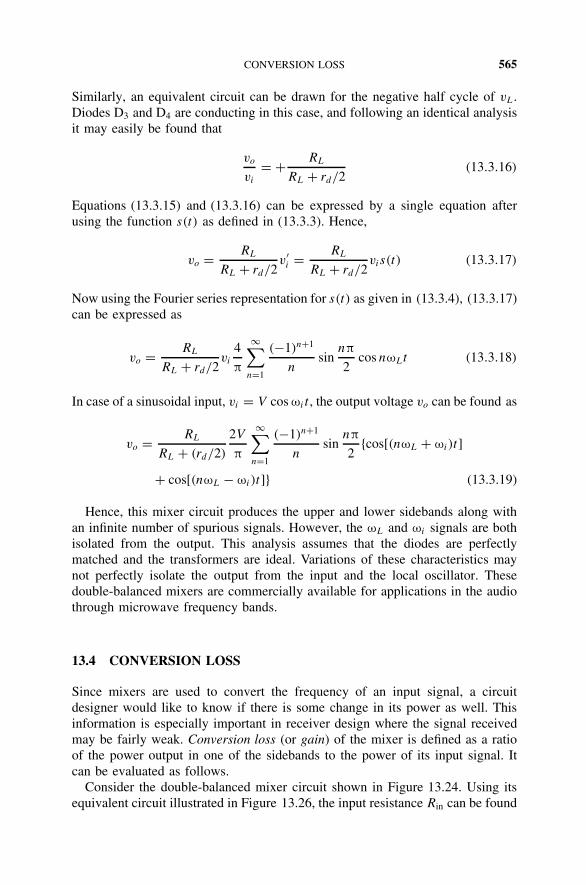
CONVERSION LOSS 565
Similarly, an equivalent circuit can be drawn for the negative half cycle of vL.Diodes D3 and D4 are conducting in this case, and following an identical analysisit may easily be found that
vo
vi
= + RL
RL + rd/2(13.3.16)
Equations (13.3.15) and (13.3.16) can be expressed by a single equation afterusing the function s(t) as defined in (13.3.3). Hence,
vo = RL
RL + rd/2v′
i = RL
RL + rd/2vis(t) (13.3.17)
Now using the Fourier series representation for s(t) as given in (13.3.4), (13.3.17)can be expressed as
vo = RL
RL + rd/2vi
4
π
∞∑n=1
(−1)n+1
nsin
nπ
2cos nωLt (13.3.18)
In case of a sinusoidal input, vi = V cos ωi t , the output voltage vo can be found as
vo = RL
RL + (rd/2)
2V
π
∞∑n=1
(−1)n+1
nsin
nπ
2cos[(nωL + ωi )t]
+ cos[(nωL − ωi )t] (13.3.19)
Hence, this mixer circuit produces the upper and lower sidebands along withan infinite number of spurious signals. However, the ωL and ωi signals are bothisolated from the output. This analysis assumes that the diodes are perfectlymatched and the transformers are ideal. Variations of these characteristics maynot perfectly isolate the output from the input and the local oscillator. Thesedouble-balanced mixers are commercially available for applications in the audiothrough microwave frequency bands.
13.4 CONVERSION LOSS
Since mixers are used to convert the frequency of an input signal, a circuitdesigner would like to know if there is some change in its power as well. Thisinformation is especially important in receiver design where the signal receivedmay be fairly weak. Conversion loss (or gain) of the mixer is defined as a ratioof the power output in one of the sidebands to the power of its input signal. Itcan be evaluated as follows.
Consider the double-balanced mixer circuit shown in Figure 13.24. Using itsequivalent circuit illustrated in Figure 13.26, the input resistance Rin can be found

566 DETECTORS AND MIXERS
with the help of (13.3.13) as follows:
Rin = vi
i1 − i2= RL + rd
2≈ RL (13.4.1)
It is assumed here that load resistance RL is much larger than the forward resis-tance rd of the diode.
If there is maximum power transfer from the voltage source vG at the inputto the circuit, the source resistance RG must be equal to the input resistance Rin.Since the input resistance is equal to the load RL, the following condition mustbe satisfied:
RG = RL
If the sinusoidal source voltage vG has a peak value of VP , it divides betweentwo equal resistances RG and Rin, and only half of voltage VP appears acrossthe transformer input. Hence,
Pi = V 2P
8RL
(13.4.2)
From (13.3.19), the peak output voltage Vo of the sideband is
Vo|ωL±ωi= 2V
π= VP
π(13.4.3)
Therefore, the output power Po is found as
Po = V 2P
2π2RL
(13.4.4)
If G is defined as the conversion gain, which is a ratio of its output to inputpower, then from (13.4.2) and (13.4.4) we find that
G = Po
Pi
= V 2P
2π2RL
8RL
V 2P
= 4
π2(13.4.5)
Since G is less than unity, it is really not a gain but a loss of power. Hence, theconversion loss, L, is
L = 10 logπ2
4= 3.92 dB ≈ 4 dB (13.4.6)
Hence, approximately 40% of the power of the input signal is transferred tothe output of an ideal double-balanced mixer. Circuit loss and mismatch reduceit further.
In the case of a single-balanced mixer where the local oscillator is isolatedfrom the output, the sideband voltage can be found from (13.3.10). Hence, the

INTERMODULATION DISTORTION IN DIODE-RING MIXERS 567
power output in one of the sidebands is given as
Po = 1
2RL
(V
π
)2
= V 2P
8π2RL
(13.4.7)
Since the input power is still given by (13.4.2), its conversion gain may befound as
G = Po
Pi
= V 2s
8π2RL
× 8RL
V 2s
= 1
π2(13.4.8)
Again, the output is less than the input power, and therefore, it represents a lossof signal power. The conversion loss for this case is
L = 10 log π2 = 9.943 ≈ 10 dB (13.4.9)
Hence, the conversion loss in this single-balanced mixer is 6 dB (four times)larger than that of the double-balanced mixer considered earlier. It may be notedthat the mixer circuit shown in Figure 13.19 has a conversion loss of only 4 dB.
These results show that the maximum possible power transferred from theinput to the output of a diode mixer is less than 40%. Therefore, these circuitsalways have conversion loss. A conversion gain is possible only when a transistor(BJT or FET) circuit is used as the mixer. FET mixers are described briefly laterin the chapter.
13.5 INTERMODULATION DISTORTION IN DIODE-RING MIXERS
As discussed in Chapter 2, the noise level defines the lower end of the dynamicrange of a system, whereas the distortion determines its upper end. Therefore, acircuit designer needs to know the distortion introduced by the mixer and whetherthere is some way to limit that. We consider here the mixer circuit depicted inFigure 13.28, which has a resistance R in series with each diode.
+
vG
RG
vi
vi
RL
vL v
vo
−
+
−
vi
+
−
+
−
D4
D3
D1
D2+
−
R
Localoscillator
R
R
R
Figure 13.28 Mixer circuit with resistance R in each branch.

568 DETECTORS AND MIXERS
R
R
+ −
D1
D2
v+ vo
vL
vi
− +
−
iL − i
iL + i
RL
Ro
Figure 13.29 Simplified equivalent of the circuit shown in Figure 13.28 for vL > 0.
Assuming that vL is large enough that the local oscillator alone controls theconduction through the diodes, an equivalent circuit can be drawn for each halfcycle. In the case of a positive half period of vL, the simplified equivalent circuitmay be drawn as illustrated in Figure 13.29. Diodes D1 and D2 conduct for thisduration while the other two are in the off state. Assume that iL is current due tovL and i is due to vi . Hence, currents through the diodes are given as follows:
current through diode D1 = id3 = iL − i
current through diode D2 = id4 = iL + i
Since the V –I characteristic of a diode is given as
id = Is(eαvd − 1) ≈ Ise
αvd (13.5.1)
whereα = q
nkT(13.5.2)
we find that
vd = 1
αln
id
Is
(13.5.3)
Note that net current flowing through the load resistance RL is the difference oftwo loop currents: iL − i and iL + i. Hence, the LO current through RL cancelsout, and two components of current due to vi are added to make it 2i. Loopequations for the circuit can be found to be
vL = (iL − i)R + vd3 + vi − RL · 2i (13.5.4)
and
vL = RL · 2i − vi + R(iL + i) + vd4 (13.5.5)
Subtracting (13.5.5) from (13.5.4), we have
0 = −2(R + 2RL)i + 2vi + vd3 − vd4

INTERMODULATION DISTORTION IN DIODE-RING MIXERS 569
or
2(R + 2RL)i − 2vi = 1
α
(ln
iL − i
Is
− lniL + i
Is
)= −1
αln
iL + i
iL − i
or
vi = (R + 2RL)i + 1
2αln
iL + i
iL − i(13.5.6)
Since the LO current iL is very large compared with i, it can be expanded as aninfinite series:
vi =(
R + 2RL + 1
αiL
)i + 1
3αi3L
i3 + 1
5αi5L
i5 + · · · (13.5.7)
An inverse series solution to this can easily be found with the help of computersoftware (such as Mathematica) as follows:
i = vi
R + 2RL + 1/αiL− v3
i
3αi3L (R + 2RL + 1/αiL)4 + · · · (13.5.8)
Therefore, the output voltage vo can be written as
vo = 2RLi = 2RL
[vi
R + 2RL + 1/αiL− v3
i
3αi3L (R + 2RL + 1/αiL)4 + · · ·
](13.5.9)
On comparing it with (2.5.31), we find that the term responsible for the inter-modulation distortion (IMD) is
k3 = − 2RL
3αi3L (R + 2RL + 1/αiL)4 (13.5.10)
Since the IMD is directly proportional to the cube of k3, (13.5.10) must beminimized to reduce the intermodulation distortion. One way to achieve thisobjective is to use a large local oscillator current iL. Another possible way isto employ the resistance R in series with each diode. Sometimes an additionaldiode is used in place of R. This permits higher local oscillator drive levels anda corresponding reduction in IMD.
Example 13.4 In the mixer circuit shown in Figure 13.30, transformer anddiodes are ideal. The transformer has 400 turns on its primary and 800 turnswith a center tap on its secondary side. Find the output voltage and the value ofload RL that provides maximum power transfer from vs .
SOLUTION For maximum power transfer, the impedance when transformed tothe primary side of the transformer must be equal to 50 . Since the number ofturns on either side of the center tap is the same as on its primary side and onlyone of the diodes is conducting at a given time, the load resistance RL must be

570 DETECTORS AND MIXERS
vLvsvo
50 Ω
RL
RL
vi
vi
Figure 13.30 Mixer circuit for Example 13.4.
50 as well. Under this condition, only half of the signal voltage appears acrossthe primary. Hence, vi = vs /2.
Assume that vL is large compared with vi such that diode switching is con-trolled solely by the local oscillator. Therefore,
vo =vL + vi for vL > 0−(vL + vi) for vL < 0
This output voltage can be expressed as follows:
vo = (vL + vi)s(t)
where
s(t) =
1 vL > 0−1 vL < 0
We already know the Fourier series representation for this s(t), given by (13.3.4)as
s(t) = 4
π
∞∑n=1
(−1)n+1
nsin
nπ
2cos nωLt (13.3.4)
If vi and vs are sinusoidal voltages
vi = Vi cos ωi t
and
vL = VL cos ωLt
then the output voltage will be
vo = (Vi cos ωi t + VL cos ωLt)4
π
∞∑n=1
(−1)n+1
nsin
nπ
2cos nωLt

FET MIXERS 571
or
vo = 2
π
∞∑n=1
(−1)n+1
nsin
nπ
2Vi[cos(nωL + ωi )t + cos(nωL − ωi )t]
+ VL[cos(nωL + ωL)t + cos(nωL − ωL)t]
13.6 FET MIXERS
Diodes are commonly used in mixer circuits because of certain advantages,including a relatively low noise. A major disadvantage of these circuits is theconversion loss, which cannot be reduced below 4 dB. On the other hand, tran-sistor circuits can provide a conversion gain, although they may be noisier. Awell-designed FET mixer produces less distortion than do BJT circuits. Further,the range of its input voltage is generally much higher (10 times or so) withrespect to BJT mixers. The switching and resistive types of mixer have beendesigned using the FET. In this section we present an overview of selected FETmixer circuits.
Figure 13.31 shows a FET mixer circuit. Local oscillator signal vL is appliedto the source terminal of the FET via capacitor C1 while the input v2 is connectedto its gate. For the FET operating in saturation, we can write
iD = IDSS
(1 − Vgs
Vp
)2
(13.6.1)
where iD is the drain current of the FET, Vgs the gate-to-source voltage, Vp itspinch-off voltage, and IDSS the drain current for Vgs = 0. For the circuit shownin Figure 13.31, the total gate voltage Vgs is
Vgs = vi − vL + VGS
vL
vi
vo
RGRS
VDD
C2
C1
Figure 13.31 FET mixer circuit.

572 DETECTORS AND MIXERS
where VGS is the gate-to-source dc bias voltage. Therefore, the drain current iDin this case is
iD = IDSS
(1 − vi − vL + VGS
Vp
)2
(13.6.2)
For sinusoidal vi and vL given as
vi = Vi cos ωi t
and
vL = VL cos ωLt
the drain current iD can be found from (13.6.2). Hence,
iD = IDSS
[1 − Vi cos ωi t − VL cos ωLt + VGS
Vp
]2
or
iD = IDSS
1 − 2
Vp
[Vi cos ωi t − VL cos ωLt + VGS]
+ IDSS
V 2p
[V 2GS + 2VGSVi cos ωi t + V 2
i cos2 ωi t − 2VLVGS cos ωLt
+ V 2L cos2 ωLt − 2ViVL cos ωi t cos ωLt] (13.6.3)
Equation (13.6.3) can be rearranged in the following form and then the amplitudesof sum and difference frequency components can easily be identified as follows:
iD = IDC + a1 cos ωi t + a2 cos ωLt + b1 cos 2 ωi t + 2 cos 2 ωLt
− ccos[(ωL + ωi )t] + cos[(ωL − ωi )t]
where
c = IDSSViVL
V 2p
(13.6.4)
The ratio of amplitude c to input voltage Vi is defined as the conversion transcon-ductance gc. Hence,
gc = c
Vi
= IDSSVL
V 2p
(13.6.5)
For high conversion gain, gc must be large. It appears from (13.6.5) that theFET with high IDSS should be preferable, but that is generally not the case. IDSS
and Vp of a FET are related such that the device with high IDSS also has highVp. Therefore, it may result in a lower gc than that of a low IDSS device. VL

FET MIXERS 573
is directly related to the conversion gain. Hence, higher local oscillator voltageincreases the conversion gain. Since the FET is to be operated in its saturationmode (the constant-current region), VL must be less than the magnitude of thepinch-off voltage.
As a special case, if VL = |Vp|/2, the conversion transconductance may befound as
gc = IDSS
2Vp
(13.6.6)
Since the transconductance gm of a JFET is given as
gm = ∂iD
∂VGS
= −2IDSS
Vp
(1 − VGS
Vp
)(13.6.7)
and
gm|VGS=0 = −2IDSS
Vp
(13.6.8)
the conversion transconductance is one-fourth of the small-signal transconduc-tance evaluated at VGS = 0 (provided that VL = 0.5Vp). For a MOSFET, it canbe shown that the conversion transconductance cannot exceed one-half of thesmall-signal transconductance.
Note from (13.6.3) that there are fundamental terms of input as well as localoscillator frequencies, their second-order harmonics, and the desired ωi ± ωL
components. Unlike the diode mixer, higher-order spurious signals are not presentin this output. In reality, there is some possibility for those terms to be presentbecause of the circuit imperfections.
An alternative to the circuit shown in Figure 13.31 combines the local oscillatorsignal with the input before applying it to the gate of FET. The analysis of thiscircuit is similar to the one presented above. In either case, one of the seriousproblems is isolation among the three signals. There have been numerous attemptsto address those problems.
Example 13.5 A given JFET has IDSS = 50 mA and transconductance gm =200 mS when its gate voltage VGS is zero. If it is being used in a mixer that hasa 50- load, find the conversion gain of the circuit.
SOLUTION Since
gm|VGS=0 = −2IDSS
Vp
then
Vp = 2 × 50 × 10−3
200 × 10−3= 1
2= 0.5 V

574 DETECTORS AND MIXERS
If the local oscillator voltage VL is kept at approximately 0.25 V, the conversiontransconductance gc may be found as
gc = 50 × 10−3
2 × 0.5= 50 × 10−3S = 50 mS
Therefore, the magnitude of voltage gain Av is
Av ≈ gcRL = 50 × 10−3 × 50 = 2.5
Since a common-gate configuration of the FET is generally used in the mixercircuit, its current gain is close to unity. Therefore, the conversion power gainof this circuit is approximately 2.5.
A dual-gate FET is frequently employed in a mixer circuit. There are sev-eral circuit configurations and modes of operation for dual-gate FET mixers.Figure 13.32 illustrates a circuit that usually performs well in most receiverdesigns. The working of this circuit can be explained considering that a dual-gate FET represents two single-gate transistors connected in cascode. Hence, theupper FET works as a source follower and the lower one provides mixing. AnRF signal is applied to a gate that is close to the ground while the local oscillatoris connected at the other gate (one close to the drain in common-source config-uration). If RF is connected to the other gate, the drain resistance of the lowertransistor section appears as source resistance and thus reduces the signal.
This circuit is used as a mixer when both transistors are operating in their triode(nonsaturation) mode. A bypass circuit is needed before its output to block theinput (RF) and the local oscillator signals. Further, another bypass circuit maybe needed across the local oscillator to block the output frequencies. This circuithas lower gain and higher noise, but a properly designed mixer can achieve amodestly higher third-harmonic intercept compared with a single-gate mixer.
Figure 13.33 shows a FET mixer circuit that employs two transistors and trans-formers. A local oscillator signal is applied to both transistors in the same phasewhile one RF input is out of phase with respect to the other. The resulting out-put is a differential of the two sides, and therefore the local oscillator signal is
Matchingnetwork
Matchingnetwork
Matchingnetwork
Outputvo
Local oscillatorvL
RF inputvi
Figure 13.32 Dual-gate FET mixer.

FET MIXERS 575
vL
vi vo+ VDD
Rs
RL
Figure 13.33 FET balanced mixer.
canceled out while the RF is added. The nonlinear characteristic of the transistorsgenerates the upper and lower sideband signals.
If the dc bias voltage at the source is VS , the RF input is Vi cos ωi t , and thelocal oscillator voltage is VL cos ωLt , the output voltage of this circuit is
vo =(
4RLVi
VP
+ 4RLViVS
V 2P
)cos ωi t + 2RLViVL
V 2P
× [cos(ωL + ωi )t + cos(ωL − ωi )t] (13.6.9)
This shows that the output of this circuit contains the RF input frequency alongwith two sidebands. Asymmetry and other imperfection can add more frequencycomponents as well.
Figure 13.34 illustrates an active double-balanced circuit, known as the Gilbertcell mixer, commonly employed in radio-frequency integrated circuits (RFICs).Transistors Q1 and Q2 are used to convert the RF voltage to current, and Q3
to Q6 are used for the switching. RF and local oscillator signals are applied tothe circuit via the corresponding matching networks (baluns). Similarly, the IFoutput requires a matching network as well. A detailed analysis of the circuit isbeyond the scope of this book; only a qualitative analysis is presented here.
Assume that the local oscillator signal is a large square wave that can turn onthe transistors when it is high and turn them off when it is low. Note that thecurrent iif1 is the sum of i3 and i5, and iif2 is the sum of i4 and i6. Further, theRF current i1 is the sum of i3 and i4 and the sum of i5 and i6 is equal to i2. Thebias current Ib is the sum of i1 and i2. Since a transistor is on only when thelocal oscillator signal is high, transistors Q4 and Q5 will be on while Q3 and Q6
will be in off conditions. Therefore,
iif1 = i5 = i2
and
iif2 = i4 = i1

576 DETECTORS AND MIXERS
Balun
BalunRF
IF
LO Q3
Q1 Q2
Q4 Q5 Q6
Ib
i3i5 i6
i1 i2
i4
VDD
RD
RD
iif1iif2
Balun
Figure 13.34 Gilbert cell mixer circuit.
Similarly, when the local oscillator signal is low, transistors Q3 and Q6 will beon and Q4 and Q5 will be off. Therefore,
iif1 = i3 = i1
and
iif2 = i6 = i2
Hence the IF output vif can be found to be
vif =RD(i2 − i1) vL > 0RD(i1 − i2) vL < 0
(13.6.10)
or
vif = RD(i2 − i1)s(t) (13.6.11)
where s(t) is defined by (13.3.3) and (13.3.4). Further, the conversion gain Gc
of this circuit can be found after assuming that it is symmetrical, and thereforethe transconductance gm of Q1 is the same as that of Q2. It is given as
Gc = 4
πgmRD (13.6.12)

PROBLEMS 577
SUGGESTED READING
Bahl, I. J., and P. Bhartia, Microwave Solid State Circuit Design. New York: Wiley, 1988.Collin, R. E., Foundations for Microwave Engineering. New York: McGraw-Hill, 1992.
Larson, L. E. (ed.), RF and Microwave Circuit Design for Wireless Communications.Boston: Artech House, 1996.
Leung, B., VLSI for Wireless Communication. Upper Saddle River, NJ: Prentice Hall,2002.
Maas, S. A., Microwave Mixers. Boston: Artech House, 1993.
Pozar, D. M., Microwave Engineering. New York: Wiley, 1998.Rohde, U. L., Microwave and Wireless Synthesizers. New York: Wiley, 1997.Smith, J. R., Modern Communication Circuits. New York: McGraw-Hill, 1998.
Vendelin, G. D., A. Pavio, and U. L. Rhode, Microwave Circuit Design Using Linear andNon-linear Techniques. New York: Wiley, 1990.
PROBLEMS
13.1. In an AM signal, the carrier output is 1 kW. If the wave modulation is100%, determine the power in each sideband. How much power is beingtransmitted?
13.2. Assume that an AM transmitter is modulated with a video signal givenby m(t) = −0.15 + 0.7 sin ω1t , where f1 is 4 MHz. Let the unmodulatedcarrier amplitude be 100 V. Evaluate and sketch the spectrum of modu-lated signal.
13.3. An AM broadcast station that uses 95% modulation is operating at totaloutput power of 100 kW. Find the power transmitted in its sidebands.
13.4. With a modulation index of 80% an AM transmitter produces 15 kW.How much of this is carrier power? Find the percentage power saving ifthe carrier and one of the sidebands are suppressed before transmission.
13.5. When an AM station transmits an unmodulated carrier, the current throughits antenna is found to be 10 A. It increases to 12 A with a modulatedsignal. Determine the modulation index used by the station.
13.6. In the circuit arrangement shown in Figure P13.6, Vout = V1 − V2 is theoutput signal, where V1 = 10VC + 0.2VCVm and V2 = 6VC − 0.2VCVm.
V1 V2VC = C cos ωct
Vout
Vm = M cos ωmt
Figure P13.6
578 DETECTORS AND MIXERS
(a) Calculate the value of M that results in a modulation index of 0.8.(b) Determine the value of C that results in an unmodulated output volt-
age amplitude of 8 V.(c) If this Vout is applied to a 50- load, find the power in the carrier and
in each sideband.
13.7. The circuit shown in Figure P13.7 uses a zero-biased diode with Rj =500 , and n = 1 at 290 K. If the signal applied to this circuit is
vin(t) = 0.5[1 + 0.3 cos(4π × 104t + 0.15)] cos(π × 109t − 0.15) V
find the output voltage vout. Also, sketch the frequency spectra of vin andvout.
vin vout
1 kΩ 31.83 pF
Figure P13.7
13.8. A 1-MHz carrier signal is amplitude-modulated simultaneously with 300-Hz, 800-Hz, and 2-kHz sinusoidal signals. What frequencies are presentin the output?
13.9. An AM broadcast transmitter radiates 50 kW of carrier power. If themodulation index is 0.85, find the power radiated.
13.10. An FM broadcast station uses a 10-kHz audio signal of 2 V peak valueto modulate the carrier. If the allowed frequency deviation is 20 kHz,determine the bandwidth requirement.
13.11. A frequency modulator is supplied with a carrier of 10 MHz and a 1.5-kHz audio signal of 1 V. The frequency deviation at its output is foundto be ±9 kHz.(a) An FM wave from the modulator is passed through a series of fre-
quency multipliers with a total multiplication of 15 (i.e., fo = 15fc).Determine the frequency deviation at the output of the multiplier.
(b) An output of the modulator is mixed with a 58-MHz signal. Find thesum frequency output of the mixer and its frequency deviation.
(c) Find the modulation index at the output of the modulator.(d) The audio input to the modulator is changed to 500 Hz with its ampli-
tude at 2 V. Determine the modulation index and frequency deviationat the output of the modulator.
13.12. An FM signal,
vFM(t) = 1500 cos[2π × 109t + 2 sin(3π × 105)] V

PROBLEMS 579
is applied to a 75- antenna. Determine (a) the carrier frequency, (b) thetransmitted power, (c) the modulation index, and (d) the frequency of themodulating signal.
13.13. When the modulating frequency in FM is 400 Hz and the modulatingvoltage is 2.4 V, the modulation index is 60. Calculate the maximumdeviation in frequency. What is the modulation index when the mod-ulating frequency is reduced to 250 Hz and the modulating voltage issimultaneously raised to 3.2 V?
13.14. The iD –Vgs characteristics of a FET are given by
iD = 7
(1 − 2Vgs
7
)2
mA
If it is being used in a mixer that has a 50- load, find the conversiongain of the circuit.
13.15. Calculate the conversion loss of the double-balanced mixer shown inFigure P13.15. The diode ON resistance is much less than the load resis-tance RL. What value of RL is required for maximum power transfer ifthe transformer employed in the circuit has 400 turns in its primary and800 turns with a center tap on its secondary side?
vLvsvo
50 Ω
RL
RL
vi
vi
Figure P13.15
13.16. In the mixer circuit shown in Figure P13.16, the transformer and diodesare ideal. The transformer has 200 turns on each side. Find the value ofRL that provides maximum power transfer from the source.
vLvsvo
75 Ω
RL
RL
vi
vi
Figure P13.16
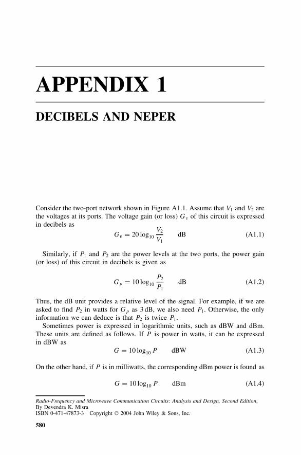
APPENDIX 1DECIBELS AND NEPER
Consider the two-port network shown in Figure A1.1. Assume that V1 and V2 arethe voltages at its ports. The voltage gain (or loss) Gv of this circuit is expressedin decibels as
Gv = 20 log10V2
V1dB (A1.1)
Similarly, if P1 and P2 are the power levels at the two ports, the power gain(or loss) of this circuit in decibels is given as
Gp = 10 log10P2
P1dB (A1.2)
Thus, the dB unit provides a relative level of the signal. For example, if we areasked to find P2 in watts for Gp as 3 dB, we also need P1. Otherwise, the onlyinformation we can deduce is that P2 is twice P1.
Sometimes power is expressed in logarithmic units, such as dBW and dBm.These units are defined as follows. If P is power in watts, it can be expressedin dBW as
G = 10 log10 P dBW (A1.3)
On the other hand, if P is in milliwatts, the corresponding dBm power is found as
G = 10 log10 P dBm (A1.4)
Radio-Frequency and Microwave Communication Circuits: Analysis and Design, Second Edition,By Devendra K. MisraISBN 0-471-47873-3 Copyright 2004 John Wiley & Sons, Inc.
580

DECIBELS AND NEPER 581
Two-portnetwork
V1 V2
Figure A1.1 Two-port network.
Thus, the dBW and dBm units represent power relative to 1 W and 1 mW, respec-tively.
Another decibel unit that is commonly used to specify phase noise of anoscillator or strengths of various sidebands of a modulated signal is dBc. Itspecifies the signal strength relative to the carrier. Consider a 100-MHz oscillatorthat has an output power of −10 dBm. Suppose that its output power is −30 dBmin the frequency range 105 to 106 MHz; then power per hertz in the outputspectrum is −90 dBm and the phase noise is −80 dBc.
In general, if amplitudes of the sideband and the carrier are given as V2 andVc, respectively, the sideband in dBc is found as
G2 = 20 logV2
Vc
(A1.5)
Consider now a 1-m-long transmission line with its attenuation constant α. If V1
is the signal voltage at its input port, the voltage V2 at its output is given as
|V2| = |V1|e−α (A1.6)
Therefore, the voltage gain Gv of this circuit in nepers is
Gv(NP) = ln|V2||V1| = −α NP (A1.7)
On the other hand, Gv in decibels is found to be
Gv(dB) = 20 log|V2||V1| = 20 log e−α = −20α log e = −8.6859α dB
Therefore,1NP = 8.6859 dB (A1.8)
The negative sign indicates that V2 is smaller than V1 and there is loss of signal.

APPENDIX 2CHARACTERISTICS OF SELECTEDTRANSMISSION LINES
COAXIAL LINE
Consider a coaxial line with its inner and outer conductor radii a and b, respec-tively, as illustrated in Figure A2.1. Further, εr is the dielectric constant of theinsulating material. The line parameters L, R, C, and G of this coaxial line arefound as follows:
C = 55.63εr
ln(b/a)pF/m (A2.1)
and
L = 200 lnb
anH/m (A2.2)
If the coaxial line has small losses due to imperfect conductor and insulator, itsresistance and conductance parameters can be calculated as follows:
R ≈ 10
(1
a+ 1
b
)√fGHz
σ/m (A2.3)
and
G = 0.3495εrfGHz tan δ
ln(b/a)S/m (A2.4)
Radio-Frequency and Microwave Communication Circuits: Analysis and Design, Second Edition,By Devendra K. MisraISBN 0-471-47873-3 Copyright 2004 John Wiley & Sons, Inc.
582

CHARACTERISTICS OF SELECTED TRANSMISSION LINES 583
εr b
a
Figure A2.1 Coaxial line geometry.
where tan δ is the loss tangent of the dielectric material, σ the conductivity ofthe conductors in S/m, and fGHz the signal frequency in GHz. The characteristicimpedance and propagation constant of the coaxial line can be calculated easilyusing the formulas given in Chapter 3.
Attenuation constants αc and αd due to conductor and dielectric losses, respec-tively, may be determined from
αc = Rs
2√
µ0/ε0εr ln(b/a)
(1
a+ 1
b
)(A2.5)
αd = ω
2
√µ0ε0εr tan δ (A2.6)
where
Rs =√
ωµ0
2σ(A2.7)
STRIP LINE
Strip line geometry is illustrated in Figure A2.2. Insulating material of thicknessh has a dielectric constant εr . The width and thickness of the central conductingstrip are w and t , respectively. For the case of t = 0, its characteristic impedancecan be found as follows:
Z0 = 1√εr
296.1
(0.6931 + ln
1 + √x ′
1 − √x ′
)−1
0 < x ≤ 0.7
30
(0.6931 + ln
1 + √x
1 − √x
)0.7 ≤ x < 1
(A2.8)
x ′ = tanhπw
2h(A2.9)

584 CHARACTERISTICS OF SELECTED TRANSMISSION LINES
h
w
εr
t
Figure A2.2 Strip line geometry.
andx =
√1 − x ′2 (A2.10)
For the design of a strip line, the following convenient formulas can be used:
w
h= 0.6366 tanh−1
√k (A2.11)
where
k =
[(eπ/y − 2)/(eπ/y + 2)]2 0 ≤ y ≤ 1√1 − [(eπy − 2)/(eπy + 2)]4 1 ≤ y
(A2.12)
y = Z0
√εr
94.18(A2.13)
For t = 0,
w
h= 1 − 2 (A2.14)
1 = 2.5465(1 − )
√ey + 0.568
ey − 1(A2.15)
and
2 =
π
1 − 0.5 ln
[(
2 −
)2
+(
0.0796
1 − 0.26
)δ]
(A2.16)
where
= t
h(A2.17)
δ = 2
1 + 23 [/(1 − )]
(A2.18)
and y is as defined in (A2.13).

CHARACTERISTICS OF SELECTED TRANSMISSION LINES 585
MICROSTRIP LINE
The geometry of a microstrip line is illustrated in Figure A2.3. Dielectric substrateon the conducting ground is h meters high and its dielectric constant is εr . Thewidth and thickness of the conducting strip on its top are w and t , respectively.The characteristic impedance of this line can be found as follows:
Z0 =
60√εre
ln
(8h
we
+ we
4h
)for
we
h≤ 1
376.7√εre
[we
h+ 1.393 + 0.667 ln
(we
h+ 1.444
)]−1for
we
h≥ 1
(A2.19)
where
we
h=
w
h+ 0.3979
t
h
[1 + ln
(12.5664
w
t
)] w
h≤ 1
2π
w
h+ 0.3979
t
h
[1 + ln
(2h
t
)]w
h≥ 1
2π
(A2.20)
The effective dielectric constant εre of a microstrip line ranges between εr and 1because of its propagation characteristics. If the signal frequency is low such thatthe dispersion is not a problem, it can be determined as follows:
εre = 0.5[εr + 1 + (εr − 1)F
(w
h
)]− εr − 1
4.6
t
h
√h
w(A2.21)
where
F(w
h
)=
(1 + 12
h
w
)−0.5
+ 0.04(
1 − w
h
)2 w
h≤ 1
(1 + 12
h
w
)−0.5w
h≥ 1
(A2.22)
h
w
εr
t
Figure A2.3 Microstrip line geometry.

586 CHARACTERISTICS OF SELECTED TRANSMISSION LINES
If dispersion cannot be ignored, the effective dielectric constant may be foundas follows:
εre(f ) =(√
εr − √εre
1 + 4F −1.5+ √
εre
)2
(A2.23)
where
F = 40
3fGHzh
√εr − 1
0.5 +
[1 + 2 log
(1 + w
h
)]2
(A2.24)
The corresponding characteristic impedance is determined from the followingformula:
Z0(f ) = Z0εre(f ) − 1
εre − 1
√εre
εre(f )(A2.25)
Attenuation constants αc and αd for the conductor and dielectric losses, respec-tively, are determined as follows:
αc =
9.9825ζ
hZ0
√fGHz
σ
32 − (we/h)2
32 + (we/h)2Np/m
w
h≤ 1
44.1255 × 10⁻⁵ ζZ0εre
h
√fGHz
σ
[we
h+ 0.667(we/h)
(we/h) + 1.444
]Np/m
w
h≥ 1
(A2.26)
where
ζ =
1 + h
we
[1 + 1.25t
πw+ 1.25
πln
(4π
w
t
)]w
h≤ 1
2π
1 + h
we
[1 − 1.25t
πh+ 1.25
πln
(2h
t
)]w
h≥ 1
2π
(A2.27)
σ is conductivity of the conductor and fGHz is the signal frequency in GHz.
αd = 10.4766εr
εr − 1
εre − 1√εre
fGHz tan δ Np/m (A2.28)
For the design of a microstrip line that has negligible dispersion, the followingformulas may be more convenient. For A > 1.52,
w
h= 8eA
e2A − 2(A2.29)
For A ≤ 1.52,
w
h= 0.6366
B − 1 − ln(2B − 1) + εr − 1
2εr
[ln(B − 1) + 0.39 − 0.61
εr
](A2.30)

CHARACTERISTICS OF SELECTED TRANSMISSION LINES 587
where
A = Z0
84.8528
√εr + 1 + εr − 1
εr + 1
(0.23 + 0.11
εr
)(A2.31)
and
B = 592.2
Z0√
εr
(A2.32)
Experimental verification indicates that (A2.29) and (A2.30) are fairly accurateas long as t/h ≤ 0.005.

APPENDIX 3SPECIFICATIONS OF SELECTEDCOAXIAL LINES AND WAVEGUIDES
TABLE A3.1 Selected Computer, Instrumentation, and Broadcast Cables
Cable TypeRG(−) Insulation
CoreO.D.(in.)
CableO.D. (in.)
Zo
()
Capacitance(pF/ft)
Attenuation(dB/100 ft) at
400 MHz
8/U Polyethylene 0.285 0.405 50 26.0 3.89/U Polyethylene 0.280 0.420 51 30.0 4.111/U Polyethylene 0.285 0.405 75 20.5 4.258/U Polyethylene 0.116 0.195 53.5 28.5 9.559/U Polyethylene 0.146 0.242 75 17.3 5.6122/U Polyethylene 0.096 0.160 50 30.8 16.5141A/U Teflon 0.116 0.190 50 29.0 9.0142B/U Teflon 0.116 0.195 50 29.0 9.0174/U Teflon 0.060 0.100 50 30.8 20.0178B/U Teflon 0.034 0.072 50 29.0 28.0179B/U Teflon 0.063 0.100 75 19.5 21.0180B/U Teflon 0.102 0.140 95 15.0 17.0213/U Polyethylene 0.285 0.405 50 30.8 4.7214/U Polyethylene 0.285 0.425 50 30.8 4.7223/U Polyethylene 0.116 0.206 50 30.8 10.0316/U Teflon 0.060 0.098 50 29.0 20.0
Radio-Frequency and Microwave Communication Circuits: Analysis and Design, Second Edition,By Devendra K. MisraISBN 0-471-47873-3 Copyright 2004 John Wiley & Sons, Inc.
588

SPECIFICATIONS OF SELECTED COAXIAL LINES AND WAVEGUIDES 589
TABLE A3.2 Selected Semirigid Coaxial Lines
MIL-C-17FDesignation
NominalImpedance
()
DielectricDiameter
(in.)
CenterConductorDiameter
(in.)
MaximumOperatingFrequency
(GHz)Capacitance
(pF/ft)
Attenuationat 1 GHz
(dB/100 ft)
129 50 0.209 0.0641 18 29.6 7.5130 50 0.1175 0.0362 20 29.9 12133 50 0.066 0.0201 20 32 22151 50 0.037 0.0113 20 32 40154 50 0.026 0.008 20 32 60
TABLE A3.3 Standard Rectangular Waveguides
EIA NomenclatureWR (−)
Inside Dimension(in.)
TE10 Mode CutoffFrequency (GHz)
RecommendedFrequency Band for TE10
Mode
2300 23.0 × 11.5 0.2565046 0.32–0.492100 21.0 × 10.5 0.2809343 0.35–0.531800 18.0 × 9.0 0.3277583 0.41–0.621500 15.0 × 7.5 0.3933131 0.49–0.751150 11.5 × 5.75 0.5130267 0.64–0.98975 9.75 × 4.875 0.6051054 0.76–1.15770 7.7 × 3.85 0.7662235 0.96–1.46650 6.5 × 3.25 0.9077035 1.14–1.73510 5.1 × 2.55 1.1569429 1.45–2.2430 4.3 × 2.15 1.3722704 1.72–2.61340 3.4 × 1.7 1.7357340 2.17–3.30284 2.84 × 1.34 2.0782336 2.60–3.95229 2.29 × 1.145 2.5779246 3.22–4.90187 1.87 × 0.872 3.1530286 3.94–5.99159 1.59 × 0.795 3.7125356 4.64–7.05137 1.372 × 0.622 4.3041025 5.38–8.17112 1.122 × 0.497 5.2660611 6.57–9.99
90 0.9 × 0.4 6.5705860 8.20–12.575 0.75 × 0.375 7.8899412 9.84–15.062 0.622 × 0.311 9.4951201 11.9–18.051 0.51 × 0.255 11.586691 14.5–22.042 0.42 × 0.17 14.088529 17.6–26.734 0.34 × 0.17 17.415732 21.7–33.028 0.28 × 0.14 21.184834 26.4–40.022 0.244 × 0.112 26.461666 32.9–50.119 0.188 × 0.094 31.595916 39.2–59.615 0.148 × 0.074 40.058509 49.8–75.812 0.122 × 0.061 48.54910 60.5–91.910 0.1 × 0.05 59.35075 73.8–1128 0.08 × 0.04 74.44066 92.2–1407 0.065 × 0.0325 91.22728 114–1735 0.051 × 0.0255 116.47552 145–2204 0.043 × 0.0215 137.93866 172–2613 0.034 × 0.017 174.43849 217–330
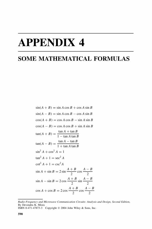
APPENDIX 4SOME MATHEMATICAL FORMULAS
sin(A + B) = sin A cos B + cos A sin B
sin(A − B) = sin A cos B − cos A sin B
cos(A + B) = cos A cos B − sin A sin B
cos(A − B) = cos A cos B + sin A sin B
tan(A + B) = tan A + tan B
1 − tan A tan B
tan(A − B) = tan A − tan B
1 + tan A tan B
sin2 A + cos2 A = 1
tan2 A + 1 = sec2 A
cot2 A + 1 = csc2A
sin A + sin B = 2 sinA + B
2cos
A − B
2
sin A − sin B = 2 cosA + B
2sin
A − B
2
cos A + cos B = 2 cosA + B
2cos
A − B
2
Radio-Frequency and Microwave Communication Circuits: Analysis and Design, Second Edition,By Devendra K. MisraISBN 0-471-47873-3 Copyright 2004 John Wiley & Sons, Inc.
590

SOME MATHEMATICAL FORMULAS 591
cos A − cos B = 2 sinA + B
2sin
B − A
22 sin A cos B = sin(A + B) + sin(A − B)
2 cos A sin B = sin(A + B) − sin(A − B)
2 cos A cos B = cos(A + B) + cos(A − B)
2 sin A sin B = cos(A − B) − cos(A + B)
sinA
2= ±
√1 − cos A
2sin 2A = 2 sin A cos A
cos 2A = cos2 A − sin2 A = 2 cos2 A − 1 = 1 − 2 sin2 A
tan 2A = 2 tan A
1 − tan2 A
cosA
2= ±
√1 + cos A
2
tanA
2= ±
√1 − cos A
1 + cos A= sin A
1 + cos A= 1 − cos A
sin A
ejA = cos A + j sin A
e−jA = cos A − j sin A
sin A = ejA − e−jA
2j= A − A3
3!+ A5
5!− A7
7!+ · · ·
cos A = ejA + e−jA
2= 1 − A2
2!+ A4
4!− A6
6!+ · · ·
tan A = je−jA − ejA
ejA + e−jA= A + A3
3+ 2
A5
15+ 17
A7
315+ · · ·
sinh A = eA − e−A
2
cosh A = eA + e−A
2
tanh A = sinh A
cos A= eA − e−A
eA + e−A
coth A = cosh A
sinh A= eA + e−A
eA − e−A
sinh(A + B) = sinh A cosh B + cosh A sinh B
cosh(A + B) = cosh A cosh B + sinh A sinh B

592 SOME MATHEMATICAL FORMULAS
sinh(A − B) = sinh A cosh B − cosh A sinh B
cosh(A − B) = cosh A cosh B − sinh A sinh B
tanh(A + B) = tanh A + tanh B
1 + tanh A tanh B
tanh(A − B) = tanh A − tanh B
1 − tanh A tanh B
cos jA = cosh A
sin jA = j sinh A
cosh2 A − sinh2 A = 1
sinh jA = j sin A
cosh jA = cos A
tanh jA = j tan A
eA = 1 + A + A2
2!+ A3
3!+ A4
4+ · · ·
e−A = 1 − A + A2
2− A3
3+ A4
4!− · · ·
sinh A = eA − e−A
2= A + A3
3!+ A5
5!+ A7
7!+ · · ·
cosh A = eA + e−A
2= 1 + A2
2!+ A4
4!+ A6
6!+ · · ·
loga xy = loga x + loga y
loga
x
y= loga x − loga y
loga xy = y loga x
loga x = logb x × loga b = logb x
logb a
ln x = log10 x × ln 10 = 2.302585 × log10 x
log10 x = ln x × log10 e = 0.434294 × ln x
e = 2.718281828

APPENDIX 5VECTOR IDENTITIES
1. Až(B × C) = Bž(C × A) = Cž(A × B)
2. A×(B × C) = B(AžC) − C(AžB)
3. ∇(φ1φ2) = φ1∇φ2 + φ2∇φ1
4. ∇ž(A × B) = Bž(∇ × A) − Až(∇ × B)
5. ∇×φA = ∇φ×A + φ(∇ × A)
6. ∇žφA = ∇φžA + φ(∇žA)
7. ∇ž(∇ × A) = 08. ∇×(∇φ) = 09. ∇ × ∇ × A = ∇(∇žA) − ∇2A
10. Stokes’s Theorem. The circulation around a simple closed curve is equalto the integral over any simple surface spanning the curve, of the normalcomponent of the curl, the positive sense on the curve being counter-clockwise as seen from the side of the surface toward which the positivenormal points. Mathematically,∮
C
Aždl =∫
S
(∇ × A)žds
11. Divergence Theorem (also known as Gauss’s theorem). The integral ofthe divergence of a vector field over a region of space is equal to the
Radio-Frequency and Microwave Communication Circuits: Analysis and Design, Second Edition,By Devendra K. MisraISBN 0-471-47873-3 Copyright 2004 John Wiley & Sons, Inc.
593

594 VECTOR IDENTITIES
integral over the surface of that region of the component of the field in thedirection of the outward directed normal to the surface. Mathematically,∫
V
(∇žA)dv =∮
S
Ažds
12. Helmholtz’s Theorem. A vector is specified uniquely if its divergenceand curl are given within a region and its normal component is given overthe boundary.
Cartesian Coordinates
∇f = x∂f
∂x+ y
∂f
∂y+ z
∂f
∂z
∇2f = ∂2f
∂x2+ ∂2f
∂y2+ ∂2f
∂z2
∇žA = ∂Ax
∂x+ ∂Ay
∂y+ ∂Az
∂z
∇ × A =
∣∣∣∣∣∣∣∣x y z∂
∂x
∂
∂y
∂
∂z
Ax Ay Az
∣∣∣∣∣∣∣∣Cylindrical Coordinates
∇f = ρ∂f
∂ρ+ φ
1
ρ
∂f
∂φ+ z
∂f
∂z
∇2f = 1
ρ
∂
∂ρ
(ρ∂f
∂ρ
)+ 1
ρ2
∂2f
∂φ2+ ∂2f
∂z2
∇žA = 1
ρ
∂(ρAρ)
∂ρ+ 1
ρ
∂Aφ
∂φ+ ∂Az
∂z
∇ × A =
∣∣∣∣∣∣∣∣ρ ρφ z∂
∂ρ
∂
∂φ
∂
∂z
Aρ ρAφ Az
∣∣∣∣∣∣∣∣Spherical Coordinates
∇f = r∂f
∂r+ θ
1
r
∂f
∂θ+ φ
1
r sin θ
∂f
∂φ
∇2f = 1
r2 sin θ
[sin θ
∂
∂r
(r2 ∂f
∂r
)+ ∂
∂θ
(sin θ
∂f
∂θ
)+ 1
sin θ
∂2f
∂φ2
]

VECTOR IDENTITIES 595
∇žA = 1
r2 sin θ
[sin θ
∂
∂r(r2Ar) + r
∂
∂θ(sin θAθ) + r
∂Aφ
∂φ
]
∇ × A = 1
r2 sin θ
∣∣∣∣∣∣∣∣r r θ r sin θφ∂
∂r
∂
∂θ
∂
∂φ
Ar rAθ r sin θAφ
∣∣∣∣∣∣∣∣

APPENDIX 6SOME USEFUL NETWORKTRANSFORMATIONS
This appendix contains transformations of networks that are commonly encoun-tered. These transformations can save time of analysis and design. Figure A6.1shows a series-connected Rs –Ls circuit transformed to a parallel-connected Rp –Lp
circuit. Resistors in the two circuits may represent loss associated with the inductor.These two circuits are equivalent if their impedance (as well as their admittance)values are equal. This equality gives
Rp = Rs + (ωLs)2
Rs
(A6.1)
and
Lp = Ls + R2s
ω2Ls
(A6.2)
Transforming the other way gives
Rs = Rp(ωLp)2
R2p + (ωLp)2
(A6.3)
and
Ls = Lp(Rp)2
R2p + (ωLp)2
(A6.4)
Radio-Frequency and Microwave Communication Circuits: Analysis and Design, Second Edition,By Devendra K. MisraISBN 0-471-47873-3 Copyright 2004 John Wiley & Sons, Inc.
596

SOME USEFUL NETWORK TRANSFORMATIONS 597
Ls
Lp Rp
Rs
Figure A6.1 Transformation of a series R–L to a shunt R–L circuit, or vice versa.
Cs
Cp RpRs
Figure A6.2 Transformation of a series R–C to a shunt R–C circuit, or vice versa.
Similarly, a series Rs –Cs circuit can be transformed to a parallel Rp –Cp
circuit, or vice versa, as illustrated in Figure A6.2. By equating their impedance(or admittance) expression, following relations may be found:
Rp = 1 + (ωCsRs)2
Rs(ωCs)2(A6.5)
and
Cp = Cs
1 + (ωCsRs)2(A6.6)
Transforming other way gives
Rs = Rp
1 + (ωCpRp)2(A6.7)
and
Cs = 1 + (ωCpRp)2
ω2CpR2p
(A6.8)
The inductor-tapped circuit shown in Figure A6.3 may be transformed to aparallel Rp –Lp circuit. This type of transformation facilitates the analysis of aHartley oscillator. Again, the impedance of an inductor-tapped circuit must beequal to that of a parallel Rp –Lp circuit. Therefore,
Rp = (ωL1L2)2 + R2(L1 + L2)
2
RL22
(A6.9)
and
Lp = (ωL1L2)2 + R2(L1 + L2)
2
ω2L1L22 + R2(L1 + L2)
(A6.10)

598 SOME USEFUL NETWORK TRANSFORMATIONS
RLp Rp
L1
L2
Figure A6.3 Transformation of an inductor-tapped circuit.
RCp Rp
C1
C2
Figure A6.4 Transformation of a capacitor-tapped circuit.
Similarly, a capacitor-tapped circuit can be transformed to a shunt Rp –Cp
circuit as illustrated in Figure A6.4. In this case, the following relations musthold if the two circuits are equal:
Rp = 1 + ω2R2(C1 + C2)2
ω2RC21
(A6.11)
and
Cp = C1[1 + ω2R2C2(C1 + C2)]
1 + ω2R2(C1 + C2)2
(A6.12)

APPENDIX 7PROPERTIES OF SOME MATERIALS
TABLE A7.1 Conductivity ofSome Materials
Material Conductivity (S/m)
Aluminum 3.54 × 10⁷
Brass 1.5 × 10⁷
Bronze 1.0 × 10⁷
Copper 5.813 × 10⁷
Gold 4.1 × 10⁷
Iron 1.04 × 10⁷
Nichrome 0.09 × 10⁷
Nickel 1.15 × 10⁷
Silver 6.12 × 10⁷
Stainless steel 0.11 × 10⁷
Radio-Frequency and Microwave Communication Circuits: Analysis and Design, Second Edition,By Devendra K. MisraISBN 0-471-47873-3 Copyright 2004 John Wiley & Sons, Inc.
599
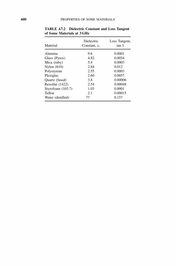
600 PROPERTIES OF SOME MATERIALS
TABLE A7.2 Dielectric Constant and Loss Tangentof Some Materials at 3 GHz
MaterialDielectric
Constant, εr
Loss Tangent,tan δ
Alumina 9.6 0.0001Glass (Pyrex) 4.82 0.0054Mica (ruby) 5.4 0.0003Nylon (610) 2.84 0.012Polystyrene 2.55 0.0003Plexiglas 2.60 0.0057Quartz (fused) 3.8 0.00006Rexolite (1422) 2.54 0.00048Styrofoam (103.7) 1.03 0.0001Teflon 2.1 0.00015Water (distilled) 77 0.157

APPENDIX 8COMMON ABBREVIATIONS
AAU analog audioABCMOS advanced bipolar CMOSABR available bit rateACI adjacent channel interferenceACTS advanced communication technology satelliteADC analog-to-digital converterADPCM adaptive differential pulse code modulationADSL asymmetric digital subscriber lineAFC automatic frequency controlAGC automatic gain controlAM amplitude modulationAMPS advanced mobile phone serviceANSI American National Standards InstituteARDIS advanced radio data information serviceASCII American Standard Code for Information InterchangeASIC application-specific integrated circuitASK amplitude-shift keyingATM asynchronous transfer modeAWGN additive white Gaussian noise
B-CDMA broadcast CDMABER bit error rateBIFET bipolar field-effect transistor
Radio-Frequency and Microwave Communication Circuits: Analysis and Design, Second Edition,By Devendra K. MisraISBN 0-471-47873-3 Copyright 2004 John Wiley & Sons, Inc.
601

602 COMMON ABBREVIATIONS
BIMOS bipolar metal-oxide semiconductorBIOS basic input–output systemBJT bipolar junction transistorBONDING bandwidth on demand interoperabilityBPSK biphase-shift keying
CAD computer-aided designCBR continuous bit rateCCD charge-coupled deviceCCIR International Radio Consultative CommitteeCDMA code-division multiple accessCDPD cellular digital packet dataCIR carrier-over-interference ratioCMOS complementary metal-oxide semiconductorCNR carrier-over-noise ratioCOB chip on boardCodec coder–decoderCRC cyclic redundancy checkCSDN circuit-switched digital networkCSMA/CD carrier sense multiple access with collision detectionCT cordless telephoneCW continuous wave
DAB digital audio broadcastDAC digital-to-analog converterDAS data acquisition systemDBS direct broadcast satelliteDCE data communication equipmentDCP data communication protocolDCPSK differentially coherent phase-shift keyingDCS-1800 digital communication system 1800DDS direct digital synthesisDECT digital European cordless telecommunicationsDFT discrete Fourier transformsDIP dual-in-line packageDMR digital mobile radioDPCM differential pulse code modulationDPSK differential phase-shift keyingDQPSK differential quadrature phase-shift keyingDRAM dynamic random access memoryDRO dielectric resonator oscillatorDSMA digital sensed multiple accessDSO digital sampling oscilloscopeDSP digital signal processingDUT device under testDWT discrete wavelet transforms

COMMON ABBREVIATIONS 603
EBS emergency broadcast systemEDA electronic design automationEIA Electronics Industries AssociationEIRP effective isotropic radiated powerEMC electromagnetic compatibilityEMI electromagnetic interferenceERC European Radio CommissionESD electrostatic dischargeESDI enhanced small device interfaceETN electronic tandem networkETSI European Telecommunication Standard Institute
FCC Federal Communications CommissionFDD frequency-division duplexFDDI fiber-distributed data interfaceFDMA frequency-division multiple accessFET field-effect transistorFFT fast Fourier transformsFH frequency hoppingFIFO first-in first-out systemFIR finite impulse response filterFM frequency modulationFPGA field-programmable gate arrayFSK frequency-shift keying
GEO geosynchronous satelliteGFSK Gaussian frequency shift keyingGIGO garbage in, garbage outGMSK Gaussian minimum shift keyingGPIB general-purpose interface busGPS global positioning systemGSM (Groupe Special Mobile) global system for mobile communicationGUI graphical user interface
HBT heterojunction bipolar transistorHDTV high-definition televisionHEMT high-electron mobility transistorHF high frequencyHIPERLAN high-performance radio LAN
I and Q in-phase and quadrature phaseIC integrated circuitsIDE integrated device electronicsIF intermediate frequencyIGBT insulated gate bipolar transistorIIT infinite impulse response filter

604 COMMON ABBREVIATIONS
IMD intermodulation distortionIMPATT impact ionization avalanche transit time diodeINTELSAT International Telecommunication Satellite ConsortiumIP intermodulation productIP Internet protocolIP2 second-order interceptIP3 third-order interceptISDN integrated services digital networkISI intersymbol interferenceISM industrial, scientific, and medical bandsITU International Telecommunication Union
JDC Japanese digital cellular standardJFET junction field-effect transistorJPEG Joint Photographic Experts Group
LAN local area networkLATA local access and transport areaLCD liquid-crystal displayLED light-emitting diodeLEOs low-Earth-orbit satelliteLHCP left-hand circular polarizationLNA low-noise amplifierLO local oscillatorLOS line of sightLUT lookup table
MAC medium access controlMAN metropolitan area networkMAU multistation access unitMBE molecular beam epitaxyMDS minimum detectable signalMDSL medium-bit-rate digital subscriber lineMEOs medium-Earth-orbit satelliteMESFET metal-semiconductor field-effect transistorMIDI musical instrument digital interfaceMIPS million instructions per secondMLC multilayer ceramicsMMI man–machine interfaceMMIC monolithic microwave integrated circuitMMSI multimode stereoscopic imagingMODFET modulation doped field-effect transistorMOSFET metal-oxide-semiconductor field-effect transistorMPEG Motion Picture Experts GroupMPP massively parallel processingMPSK minimum phase-shift keying

COMMON ABBREVIATIONS 605
MSK minimum shift keyingMSP mixed signal processorMSS mobile satellite serviceMTI moving-target indicatorMTSO mobile telephone switching officeMUX multiplexing
NADC North American Digital Cellular/CordlessNF noise figureNMT Nordic Mobile TelephoneNTSC National Television Standards CommitteeNTT Nippon Telephone and Telegraph
OFDM orthogonal frequency-division multiplexingOOK on–off keyingOOP object-oriented programming
PAD packet assembler and disassemblerPAL phase alternating linePAM pulse amplitude modulationPAMR public access mobile radioPBX private branch exchangePCB printed circuit boardPCM pulse code modulationPCMCIA Personal Computer Memory Card International AssociationPCN personal communication networkPCS personal communication servicePDA personal digital assistantPDC personal digital cellularPDIP plastic dual-in-line packagePGA programmable gain amplifier; also pin grid arrayPHP personal handy phonePHS personal handyphone system (formerly PHP)PID proportional integrating differentiatingPIN p-type, intrinsic, n-type diodePLC programmable logic controllerPLL phase-locked loopPM pulse modulationPMR private mobile radioPOTS plain old telephone servicePPGA plastic pin grid arrayPQFP plastic quad flat packPSK phase-shift keyingPSTN public switched telephone networkPVC permanent virtual connection

606 COMMON ABBREVIATIONS
PWB printed wire boardPWM pulse width modulation
QAM quadrature amplitude modulationQCELP Qualcomm coded excited linear predictive codingQDM quadrature demodulatorQMFSK quadrature modulation frequency-shift keyingQPSK quadrature phase-shift keying
RADAR radio detection and rangingRAID redundant array of independent disksRBDS radio broadcast data systemRCS radar cross sectionRES Radio Expert Systems GroupRF radio frequencyRFI radio-frequency interferenceRHCP right-handed circular polarizationRMS root mean squareRPE-LTP regular pulse excitation long-term predictorRTD resistive thermal detectorRTMS radio telephone mobile system
SAW surface acoustic waveSCSI small computer systems interfaceSDH synchronous digital hierarchySDIP shrink dual-in-line packageSDN switched digital networkSFDR spur-free dynamic rangeSINAD signal-over-noise and distortionSIP single-in-line packageSLICs standard linear integrated circuitsSMD surface-mount deviceSMR specialized mobile radioSNR signal-to-noise ratioSOI silicon on insulatorSOIC small outline integrated circuitSONET synchronous optical networkSOT small outline transistorSPLIC special-purpose linear integrated circuitSQPSK staggered quadriphase-shift keyingSQUID superconducting quantum interfaceSSB single sidebandSTP shielded twisted pairSVD simultaneous voice and dataSWR standing wave ratio

COMMON ABBREVIATIONS 607
TACS total access communication systemTCP transmission control protocolT-DAB terrestrial-digital audio broadcastingTDD time-division duplexTDMA time-division multiple accessTDR time-domain reflectometryTE transverse electricTEM transverse electromagnetic waveTETRA trans-European trunked radio systemTHD+N total harmonic distortion plus noiseTIA Telecommunications Industry AssociationTM transverse magneticTNC threaded Neil-Councilman connectorTSAPI telephony services–oriented application programming interfaceTTL transistor–transistor logicTVG time-variable gainTVRO TV receive-onlyTVS transient voltage suppressionTWTA traveling wave tube amplifierTx transmitter
UART universal asynchronous receiver/transmitterUDPC universal digital personal communicationsUHF ultrahigh frequencyUNC universal control networkUNI user-to-network interfaceUPS uninterruptible power supplyUSART universal synchronous–asynchronous receiver transmitterUSB universal serial busUTC universal time codeUTP unshielded twisted pair
VCO voltage-controlled oscillatorVDT video display terminalVHDL very high definition languageVHF very high frequencyVLF very low frequencyVLSI very-large-scale integrationVPSK variable phase-shift keyingVSAT very small aperture (satellite ground) terminalVSELP vector sum excited linear predictive codingVSWR voltage standing wave ratioVXCO voltage-controlled crystal oscillator
WAN wide area networkWATS wide area telecommunication network

608 COMMON ABBREVIATIONS
WDM wavelength-division multiplexingWER word error rateWFAU wireless fixed access unitWLAN wireless local area networkWLL wireless local loopWORM write once, read manyWPABX wireless private branch exchange

APPENDIX 9PHYSICAL CONSTANTS
Permittivity of free space, ε0 8.8542 × 10⁻¹² F/mPermeability of free space, µ0 4π × 10−7 H/mImpedance of free space, η0 376.7
Velocity of light in free space, c 2.997925 × 10⁸ m/sCharge of electron, qe 1.60210 × 10⁻¹⁹ CMass of electron, me 9.1091 × 10⁻³¹ kgBoltzmann’s constant, k 1.38 × 10⁻²³ J/KPlanck’s constant, h 6.6256 × 10⁻³⁴ J·s
Radio-Frequency and Microwave Communication Circuits: Analysis and Design, Second Edition,By Devendra K. MisraISBN 0-471-47873-3 Copyright 2004 John Wiley & Sons, Inc.
609

INDEX
1/f noise, 34Acquisition of lock, 509Admittance matrix, 289Admittance parameters, 289AM, see Amplitude modulationAmpere’s law, 105Amplitude modulation, 544
DSB, 546modulation index, 544SSB, 546suppressed carrier AM, 546
Antenna efficiency, 21Antennas, 18
Cassegrain reflector, 18directive gain, 19electric dipole, 18isotropic antenna, 19lens, 18power gain, 19pyramidal horn, 18
Attenuation constant, 62, 116Available power gain, 411
Balanced amplifier, 468Bandpass filter, 371Bandstop filter, 375Barkhausen criterion, 480
Bessel function, 143, 180, 556Binomial filter, 354Binomial transformers, 244Bisected π-section, 346Black-body radiation law, 34Bode–Fano constraints, 280Broadband amplifiers, 466Butterworth filter, 354
C3, 7Carson rule bandwidth, 556Cellular telephones, 17Chain matrix, 298Chain scattering parameters, 325Characteristic impedance, 59
experimental determination of, 75Chebyshev filter, 355Chebyshev polynomials, 250, 356Chebyshev transformers, 248, 255Clapp oscillator, 488Closed-loop gain, 480Coaxial line, 582Coefficient of coupling, 166Coherent detector, 553Colpitts oscillator, 484Complex permittivity, 112Composite filters, 346
Radio-Frequency and Microwave Communication Circuits: Analysis and Design, Second Edition,By Devendra K. MisraISBN 0-471-47873-3 Copyright 2004 John Wiley & Sons, Inc.
611

612 INDEX
Conductivity, 59, 112Conservation of charge, 107Constant gain circles, 439Constant noise figure circles, 457Constant-k, 337Constitutive relations, 111Cordless telephones, 17Critically damped, 153Current reflection coefficient, 73Current sensitivity, 551Cutoff frequency, 337, 338, 354, 360, 369Cylindrical cavity, 179Cylindrical waveguide, 137, 142
Damping ratio, 153dB, 580dBc, 581dBW, 580Dibit, 9Directivity, 19, 27Distortion, 33, 45Distortionless line, 75Distributed amplifiers, 468Distributed elements, 58Doppler radar, 11, 32Divergence theorem, 593Double-balanced mixer, 563Double-stub tuner, 202DR, see Dielectric resonatorsDynamic conductance, 550Dynamic range, 5, 11, 47
EIRP, 24Electric charge density, 105Electric current density, 105Electric field intensity, 104, 112Electric flux density, 105, 111Electric scalar potential, 128Electric vector potential, 129Electrical susceptibility, 111Equation of continuity, 107
Faraday’s law of induction, 105FDM, 543FET mixer, 571Flicker noise, 34FM, see Frequency modulationFM detector, 558Fractional bandwidth, 236Frequency bands, 2, 3Frequency converter, 547Frequency division multiplexing, 543Frequency modulation, 2, 9, 543, 555
modulation index, 555
Frequency scaling, 360Frequency-shift keying, 9Friis transmission formula, 26
Gain compression, 48Geosynchronous, 13Gilbert cell, 575Global positioning system, 15Group velocity, 65Gunn diodes, 520
Half-power beam width, 20Hankel functions, 144Hartley oscillator, 484HBT, 422Helmholtz’s equations, 62Helmholtz’s theorem, 128HEMT, 422High-pass filter, 338, 369Hybrid parameters, 296
Image impedance, 334Image parameter method, 334IMD, 569IMPATT diode, 520Impedance matrix, 284Impedance parameters, 284Impedance scaling, 361Incident wave, 64, 123Indirect frequency synthesizer, 516Input node, 396Input reflection coefficient, 68Input stability circle, 427Insertion loss, 72Insertion loss method, 353Intercept point, 50Intermediate frequency, 12Intermodulation distortion, 45, 567Intermodulation distortion ratio, 49Intrinsic impedance, 115IP, see Intercept pointIR, 2Isotropic antenna, 19
Johnson noise, 33
Klopfenstein taper, 276Kuroda’s identities, 384
Leontovich impedance boundary condition, 121LEOS, 15, 16Line-of-sight propagation, 5Load reflection coefficient, 70, 80

INDEX 613
Lock-in range, 510Loop, 398, 480Loop gain, 398, 480Loop-filters, 500Lorentz condition, 128, 130Loss-tangent, 112Low-pass filter, 337, 354Low-pass filter synthesis, 358Low-pass ladder network prototype, 358
Magnetic charge, 126Magnetic current, 126Magnetic field intensity, 104Magnetic flux density in, 105Magnetic scalar potential, 129Magnetic susceptibility, 112Magnetic vector potential, 127Magnetization density, 112Maximally flat filter, 354Maximally flat low-pass filters, 355Maxwell’s equations, 109, 110m-derived filter, 341MEOS, 15Microstrip line, 585Microwave transistor oscillator, 523Minimum detectable signal, 44Minkowski inequality, 424Mixer, 9, 12Mixers:
conversion loss, 565diode ring, 567dual gate FET, 574FET mixers, 571intermodulation distortion, 569single diode, 548switching type, 559
Negative resistance, 489Neper, 581Neumann function, 143Noise, 33Noise factor, 37Noise figure, 38Noise figure of a cascaded system, 40Noise figure parameter, 458Noise in two-port networks, 39Noise temperature, 35Nonredundant circuit synthesis, 380Normalized image impedance, 344Normalized input impedance, 68Notch-filter, 333Nyquist criterion, 480Nyquist noise, 33
On-off keying, 9Operating power gain, 414Output node, 396Output stability circle, 426Overdamped, 153
Parallel-plate waveguide, 133Path, 398Path gain, 398Personal communication networks, 16Personal handy phone, 17Phase constant, 62, 114Phase detector, 498Phase modulation, 9Phase velocity, 65, 115Phase-locked loop, 497Phase-shift keying, 9Pierce oscillator, 494Pink noise, 34Polarization, 23Polarization density, 111Power density, 19Power flow, 113Power loss ratio, 353Poynting’s vector, 113Propagation constant, 62, 116
experimental determination of, 75Pull-in range, 510Pulling figure, 494
Q, see Quality factorQuadrature phase-shift keying, 9Quality factor, 155Quarter-wavelength transformer, 70
Radar, 4Radar cross-sections, 29Radar range equation, 29Radiation efficiency, 22Radiation field, 19Radiation intensity, 19Radiation pattern, 20Radio frequency detector, 551Radio frequency identification, 2Rayleigh–Jeans approximation, 34Reactive L-section matching, 209Receiver, 8Rectangular cavity, 177Redundant filter synthesis, 380Reflected wave, 64Reflection coefficient, 68Remote sensing, 7Repeater, 12Resistive L-section matching, 207

614 INDEX
Resonant frequency, 179Return-loss, 72Reverse-saturation current, 549Richard’s transformation, 384
Sampling theorem, 272Satellite communication, 13Scattering matrix, 306Scattering parameters, 306
shifting of reference planes, 311Scattering transfer parameters, 325Second harmonic distortion, 48Self-loop, 398Semirigid coaxial lines, 589Shot noise, 33Shunt matching element, 190Shunt stub matching, 190Signal flow graph, 392
branches, 392junction points, 392Mason’s rule, 399nodes, 663rules of reduction, 398
Signal-to-noise ratio, 37Skin depth, 115Simultaneous conjugate matching, 432Single-balanced mixer, 560Single-diode mixer circuit, 548Small-signal equivalent circuit of a BJT, 469Small-signal equivalent circuit of a MESFET,
471Small-signal equivalent circuit of a MOSFET,
470Smith chart, 85Space loss, 25Spurious-free dynamic range, 51SSB, 546Stability circle, 427Stokes’ theorem, 593Strip line, 583Stub, 189Switching-type mixers, 559Synchronization range, 507
Terrestrial communication, 12Three-port S-parameter description of the
transistor, 530Time-harmonic fields, 110
Time-period, 64Tracking range, 507Transducer power gain, 412Transmission line:
attenuation constant, 62characteristic impedance, 59distributed network model, 61line parameters, 58phase constant, 62propagation constant, 62
Transmission line equations, 61Transmission lines, 4Transmission parameters, 298Transmitter, 8Transponder, 14Traveling wave amplifiers, 468Traveling wave tube, 14Tuning sensitivity, 496
UHF, 3Undamped natural frequency, 153Underdamped, 153Unilateral figure of merit, 437Unilateral transducer power gain, 413
Varactors, 495VCO, see Voltage-controlled oscillatorVector wave equation, 114VHF, 3Voltage-controlled oscillator, 496, 497Voltage reflection coefficient, 72Voltage sensitivity, 552Voltage standing wave, 82VSAT, 15VSWR, 82
Wavelength, 64Wave number, 114Wire antennas, 18
electric dipole, 18loop antennas, 18
Wireless communication, 8, 16
Y -factor method, 36
Zero-biased diode detector, 552ZY -Smith chart, 219


