
UNLV Theses, Dissertations, Professional Papers, and Capstones
12-1-2014
Simulation, and Overload and Stability Analysis of Continuous Simulation, and Overload and Stability Analysis of Continuous
Time Sigma Delta Modulator Time Sigma Delta Modulator
Kyung Kang University of Nevada, Las Vegas
Follow this and additional works at: https://digitalscholarship.unlv.edu/thesesdissertations
Part of the Computer Sciences Commons, Digital Communications and Networking Commons, and
the Electrical and Computer Engineering Commons
Repository Citation Repository Citation Kang, Kyung, "Simulation, and Overload and Stability Analysis of Continuous Time Sigma Delta Modulator" (2014). UNLV Theses, Dissertations, Professional Papers, and Capstones. 2274. http://dx.doi.org/10.34917/7048593
This Dissertation is protected by copyright and/or related rights. It has been brought to you by Digital Scholarship@UNLV with permission from the rights-holder(s). You are free to use this Dissertation in any way that is permitted by the copyright and related rights legislation that applies to your use. For other uses you need to obtain permission from the rights-holder(s) directly, unless additional rights are indicated by a Creative Commons license in the record and/or on the work itself. This Dissertation has been accepted for inclusion in UNLV Theses, Dissertations, Professional Papers, and Capstones by an authorized administrator of Digital Scholarship@UNLV. For more information, please contact [email protected].

SIMULATION, AND OVERLOAD AND STABILITY ANALYSIS
OF CONTINUOUS TIME SIGMA DELTA MODULATOR
By
Kyung Kang
Bachelor of Engineering in Electrical Engineering
Korea University, South Korea
2001
Master of Engineering in Electrical Engineering
Korea University, South Korea
2003
A dissertation submitted in partial fulfillment of the requirements for the
Doctor of Philosophy - Electrical Engineering
Department of Electrical and Computer Engineering
Howard R. Hughes College of Engineering
The Graduate College
University of Nevada, Las Vegas
December 2014

ii
We recommend the dissertation prepared under our supervision by
Kyung Kang
entitled
Simulation, and Overload and Stability Analysis of Continuous Time Sigma Delta
Modulator
is approved in partial fulfillment of the requirements for the degree of
Doctor of Philosophy in Engineering - Electrical Engineering
Department of Electrical Engineering
Peter Stubberud, Ph.D., Committee Chair
Sahjendra Singh, Ph.D., Committee Member
Ebrahim Saberinia, Ph.D., Committee Member
R. Jacob Baker, Ph.D., Committee Member
Laxmi Gewali, Ph.D., Graduate College Representative
Kathryn Hausbeck Korgan, Ph.D., Interim Dean of the Graduate College
December 2014
iii
ABSTRACT
By
Kyung Kang
Dr. Peter Stubberud, Examination Committee Chair
Professor of Electrical and Computer Engineering
University of Nevada, Las Vegas
The ever increasing demand for faster and more powerful digital applications requires high speed,
high resolution ADCs. Currently, sigma delta modulators (ADCs are extensively used in
broadband telecommunication systems because they are an effective solution for high data-rate wireless
communication systems that require low power consumption, high speed, high resolution, and large
signal bandwidths.
Because mixed-signal integrated circuits such as Continuous Time sigma delta modulators (CT
ΣΔMs) contain both analog and digital circuits, mixed signal circuits are not as simple to model and
simulate as all discrete or all analog systems. In this dissertation, the delta transform is used to simulate
CT ΣΔMs, and its speed and accuracy are compared to the other methods. The delta transform method
is shown to be a very simple and effective method to get accurate results at reasonable speeds when
compared with several existing simulation methods.
When a CT ΣΔM is overloaded, the ΣΔM’s output signal to quantization noise ratio (SQNR)
decreases when the ΣΔM’s input is increased over a certain value. In this dissertation, the range of
quantizer gains that cause overload are determined and the values ware used to determine the input
signal power that prevents overload and the CT ΣΔM’s maximum SQNR. The CT ΣΔMs from 2nd to
5th order are simulated to validate the predicted maximum input power that prevents overload and the
maximum SQNR.
Determining the stability criteria for CT ΣΔMs is more difficult than it is for Discrete time sigma delta

iv
modulators (DT ΣΔMs) because CT ΣΔMs include delays which are modeled mathematically by
exponential functions for CT systems. In this dissertation an analytical root locus method is used to
determine the stability criteria for CT ΣΔMs. This root locus method determines the range of quantizer
gains for which a CT ΣΔM is stable. These values can then be used to determine input signal and
internal signal powers that prevent ΣΔMs from becoming unstable. Also, the maximum input power that
keeps the CT ΣΔMs stable for CT ΣΔMs operating in overload can be determined. The CT ΣΔMs from
2nd to 5th order are simulated to validate the predicted maximum input power that keeps the CT ΣΔMs
stable.

v
TABLE OF CONTENTS
ABSTRACT…………………………………………………………………………..…………...iii
TABLE OF CONTENTS…………………………………………………………..………………v
LIST OF TABLES…………………………………………………………………………..…….vii
LIST OF FIGURES……………………………………………………………...………………ix
CHAPTER 1 INTRODUCTION…………...…………………………………………………...…1
CHAPTER 2 FUNDAMENTALS OF CT ΣΔM……………………………………………….....6
2.1 Performance of Analog to Digital Converters…………………………………………6
2.1.1 Mathematical models of sampling and quantization…………………………....6 2.1.2 Oversampling………………………..…………………………………………..9
2.1.3 Overload………………………..…………………………………………....….11
2.1.4 Dynamic Range (DR)…………………………………………………………...12 2.1.5 Signal to Quantization Noise Ratio (SQNR)…………………………………....12
2.2 The Operation Principles of Sigma Delta Modulators…………………………………...14
2.3 Classification of Sigma Delta Modulators….……………………………………………19
2.3.1 Single-bit ΣΔMs versus Multi-bit ΣΔMs.……………………………………....19 2.3.2 Single-loop ΣΔMs versus Cascaded ΣΔMs.……………………………..……...20
2.3.3 2nd order ΣΔMs versus Higher order ΣΔMs.…………………………………...20
2.3.4 Lowpass ΣΔMs versus Bandpass ΣΔMs….…………………………..………...20
2.3.5 Discrete Time ΣΔMs versus Continuous Time ΣΔMs……………………….....20 2.3.6 ΣΔMs in this dissertation……………………………………………………….21
2.4 Topology Selection of the CT ΣΔM for simulations……………………………….....21
2.5 Conclusion………………………………………………………………………….....25
CHAPTER 3 A COMPARISON OF CT ΣΔM SIMULATION METHODS…………………....30
3.1 The Conventional Approaches to Simulating CT ΣΔMs…………………..………....30
3.1.1 Macromodel in SPICE………………………………………………………....30
3.1.2 Solving differential equations………………………..………………………...32
3.1.3 Implementing difference equation (CT/DT equivalence)……………………...33
3.1.4 MATLAB/Simulink………..…………………………………………………..35
3.2 Simulating CT ΣΔMs Using the Delta Operator………………………………..…..36
3.2.1 Definition of Delta Transform………………………………………………....36

vi
3.2.2 Application of Delta Transform for CT ΣΔMs simulation………………….....39
3.3 Simulation Comparison……………………………………………………………...42
CHAPTER 4 OVERLOAD ANALYSIS OF CT ΣΔMS.………………………...………….......53
4.1 Definition of Overload for a Single-bit Quantizer ……….……………………….....53
4.2 Overload Analysis………………………………………………………………..…..55
4.3 Example ……….…………………………………………………………..………...59
4.4 Other Simulation Results ……….……………………………………………..……...61
4.5 Predicting the SQNR of a ΣΔM …………………………………………………….65
4.5.1 Derivation of SQNR Approximation when operating in no-overload range….66
4.5.2 Prediction of the SQNR of a ΣΔM in overload………………………………..68
4.5.3 Simulation results…………………..………………………………………….70
CHAPTER 5 STABILITY ANALYSIS OF CT ΣΔMS……………………………………….....76
5.1 Analytical Root Locus.……………………………………………………………....77
5.1.1 Root locus equation and Gain equation……………………………..………....77
5.1.2 Illustrative example of analytical root locus……………………...…………...79
5.2 Stability Analysis for CT ΣΔMs that are not overloaded……………………………….89
5.3 Stability Analysis Example of ΣΔMs that are not overloaded…………………………..92
5.4 Other Stability Simulation Results of CT ΣΔMs that are not overloaded……………......97
5.5 Stability Analysis for overloaded CT ΣΔMs…………………………………………..99
5.6 Stability Analysis Example of an overloaded ΣΔM ………………………………..…101
5.7 Other Simulation Results of overloaded ΣΔMs ………………………………………106
5.8 Conclusion ………………………………………………………………………...108
CHAPTER 6 CONCLUSIONS………………………………...……………………………….110
REFERENCES………………………………………………………………………………….112
CURRICULUM VITAE……………………………………..……………………………….....115

vii
LIST OF TABLES
Table 2.1 Classification of ΣΔMs…………………………………........….........................19
Table 2.2 CT ΣΔM STF and NTF coefficients for RC implementations.………..…..........28
Table 2.3 CT ΣΔM STF and NTF coefficients for GmC implementations…………...........29
Table 3.1 Simulation Condition……………………………………………………............43
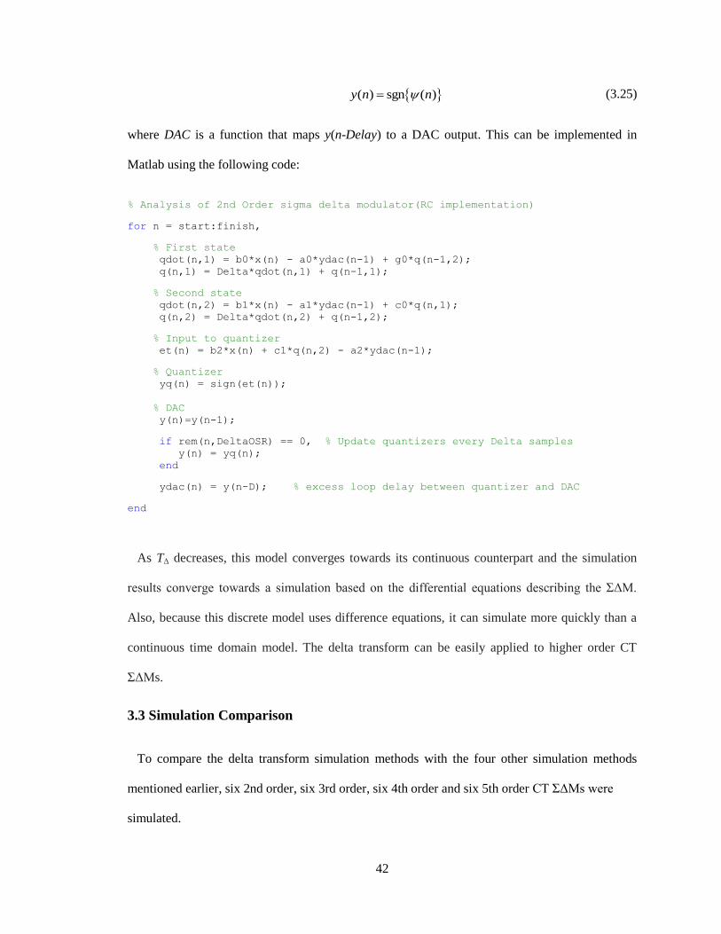
Table 3.2 The SQNR comparison of simulation methods for the 4th order CT ΣΔΜs........46
(a) Simulated SQNR
(b) The SQNR difference from the SQNR of SPICE
(c) The percentage of SQNR difference
Table 3.3 The SQNR comparison of simulation methods for the 5th order CT ΣΔΜs........47
(a) Simulated SQNR
(b) The SQNR difference from the SQNR of SPICE
(c) The percentage of SQNR difference
Table 3.4 The SQNRs comparison between RC implementation and
GmC implementation for each of simulation methods….......................................49
Table 3.5 The elapsed time comparison between RC implementation and
GmC implementation for each of simulation methods………………………......50
Table 3.6 Performance comparison of simulation methods……………………..................51
Table 4.1 Specification for each CT ΣΔΜ.............................................................................62
(a) Common specification
(b) NTF attenuation for each CT ΣΔΜ
Table 4.2 Comparison of the theoretical minimum quantizer gains and
the simulated minimum quantizer gains at predicted xmaxO....................................65
Table 4.3 Comparison of the predicted maximum sinusoidal input amplitude with
the simulated maximum sinusoidal input amplitude that prevents overloading
for the ΣΔΜs in Table 4.1.......................................................................................65
Table 5.1 F(s), G(s) and H(s) for RC implementations…………………………………......83
Table 5.2 F(s), G(s) and H(s) for GmC implementations…………………………................84
Table 5.3 Re{D(s)}, Im{D(s)}, Re{N(s)} and Im{N(s)}for RC implementations….............85
Table 5.4 Re{D(s)}, Im{D(s)}, Re{N(s)} and Im{N(s)}for GmC implementations…..........87
Table 5.5 Specification for each CT ΣΔΜ...............................................................................97
(a) Common specification
(b) NTF attenuation for each CT ΣΔΜ
Table 5.6 Comparison of the theoretical minimum quantizer gains and
the simulated minimum quantizer gains at predicted xmaxS.....................................98
Table 5.7 Comparison of the predicted maximum sinusoidal input amplitude with
the simulated maximum sinusoidal input amplitude that keeps the ΣΔΜ stable..98
Table 5.8 Comparison of the prediction and the simulation................................................107
(a) Predicted minimum stable quantizer gain and simulated quantizer gain
for sinusoidal input with predicted maximum amplitude
(b) Predicted maximum input amplitude and simulated input amplitude
at predicted KminS

viii
(c) Predicted maximum input amplitude and simulated maximum input amplitude
Table 5.9 Summary of the stability analysis for both overloaded CT ΣΔΜs
and CT ΣΔΜs that are not overloaded................................................................109
(a) Predicted minimum stable quantizer gain and simulated quantizer gain
for sinusoidal input with predicted maximum amplitude,
(b) Predicted maximum input amplitude and simulated input amplitude
at predicted KminS,
(c) Predicted maximum input amplitude and simulated maximum input amplitude,
(d) The difference between predicted maximum input amplitude and simulated
maximum input amplitude

ix
LIST OF FIGURES
Figure 2.1 Operation principles of an ADC.………………....................….....................….....7
(a) Block diagram of a classical analog to digital converter
(b) Time domain example
(c) Frequency domain example
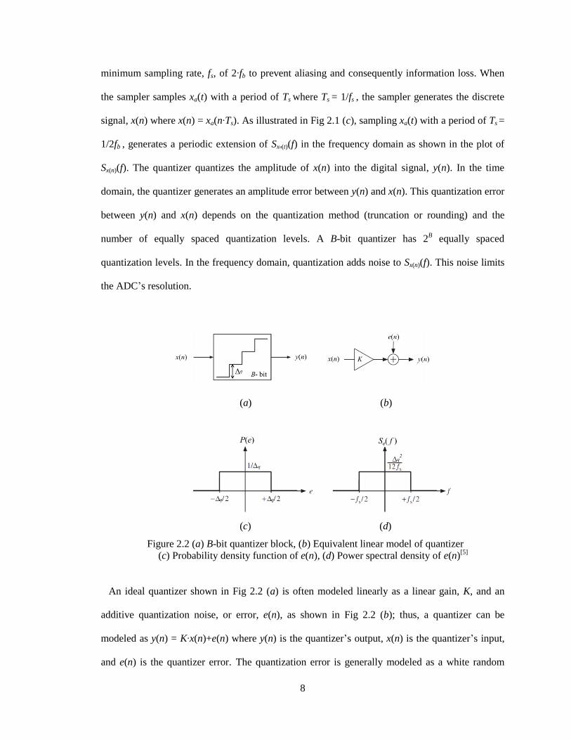
Figure 2.2 (a) B-bit quantizer block...........................................................................................8
(b) Equivalent linear model of quantizer
(c) Probability density function of e(n)
(d) Power spectral density of e(n)
Figure 2.3 Power spectral density of the total quantization noise for.....................................10
(a) a Nyquist rate ADC
(b) an oversampling ADC with OSR=2
(c) power spectral density of the quantization noise power within signal bandwidth
for an oversampling ADC with OSR=2
Figure 2.4 Transfer characteristic for a typical B-bit quantizer...............................................11
Figure 2.5 (a) Block diagram of a CT ΣΔM.............................................................................15
(b) A linear model for the CT ΣΔM’s STF
(c) A linear model for the CT ΣΔM’s NTF
Figure 2.6 STF/NTF magnitude response designed with the Chebyshev2 filter....................17
Figure 2.7 The spectra of the input signal and the quantization noise....................................18
(a) before the noise shaping, (b) after the noise shaping
Figure 2.8 2nd order lowpass CT ΣΔM block diagram...........................................................22
(a) RC implementation, (b) GmC implementation
Figure 2.9 3rd order lowpass CT ΣΔM block diagram............................................................25
(a) RC implementation, (b) GmC implementation
Figure 2.10 4th order lowpass CT ΣΔM block diagram............................................................26
(a) RC implementation, (b) GmC implementation
Figure 2.11 5th order lowpass CT ΣΔM block diagram............................................................27
(a) RC implementation, (b) GmC implementation
Figure 3.1 Macromodel of a 2nd order CT ΔΣM.………………....................…...................31
(a) Functional blocks of a 2nd order CT ΣΔM
(b) RC integrators implementation for a loop filter
(c) GmC integrators implementation for a loop filter
Figure 3.2 Circuit model of a 2nd order CT ΣΔM………………....................…...................32
Figure 3.3 Equivalence between a CT ΣΔM and a DT ΣΔM…....................….......................34
Figure 3.4 Simulink model for a 2nd order CT ΣΔΜ.…...............................….......................35
Figure 3.5 Delta operator block diagram.…...............................…..........................................38
Figure 3.6 Stability regions for the continuous Laplace plane,
and the discrete z-plane, delta-plane........................................................................39
Figure 3.7 The 2nd order CT ΣΔM block diagram.…..............................................................39
Figure 3.8 2nd order DT model ΣΔM using delta transform.…...............................................41
Figure 3.9 The output power spectra comparison for the simulation methodologies
for 2nd order CT ΣΔΜs with an excess loop delay of (a) zero, (b) 0.5T, (c) T,
(d) 1.5T, (e) 2T, (f) 2.5T.…......................................................................................44
x
Figure 3.10 Simulation comparison of the maximum SQNR for (a) 2nd order CT ΣΔΜs,
(b) 3rd order CT ΣΔΜs, (c) 4th order CT ΣΔΜs, (d) 5th order CT ΣΔΜs...........45
Figure 3.11 The output power spectra for the GmC implementation
for the 2nd order CT ΣΔΜs with an excess loop delay of zero............................48
Figure 3.12 Simulation comparison of the elapsed time to complete the simulation for
(a) 2nd order CT ΣΔΜs, (b) 3rd order CT ΣΔΜs,
(c) 4th order CT ΣΔΜs, (d) 5th order CT ΣΔΜs....................................................49
Figure 4.1 (a) The transfer characteristic for a single-bit quantizer
(b) quantization error, e of a single-bit quantizer
(c) quantizer gain, K of a single-bit quantizer........................................................54
Figure 4.2 (a) Block diagram of a CT ΣΔM’s STF
(b) Block diagram of a CT ΣΔM’s NTF.................................................................56
Figure 4.3 Bell curve of the standard normal distribution.......................................................57
Figure 4.4 The root locus of a 2nd order CT ΣΔΜ with a sampling frequency, fs,
where fs =1/T, of 1GHz and Chebyshev Type 2 NTF for
(a) D = 0, (b) D = 0.5T, (c) D = T...........................................................................59
Figure 4.5 Simulated SQNR and the minimum quantizer gain (Kmin) using a sinusoidal input
for the 2nd order CT ΣΔΜ in example....................................................................61
Figure 4.6 Simulated SQNR and the minimum quantizer gain (Kmin) using a sinusoidal input
(a) for the 2nd order CT ΣΔΜ, (b) for the 3rd order CT ΣΔΜ,
(c) for the 4th order CT ΣΔΜ, (d) for a 5th order CT ΣΔΜ with D = 0................63
Figure 4.7 Simulated SQNR and the minimum quantizer gain (Kmin) using a sinusoidal input
(a) for the 2nd order CT ΣΔΜ, (b) for the 3rd order CT ΣΔΜ,
(c) for the 4th order CT ΣΔΜ, (d) for a 5th order CT ΣΔΜ with D = T................64
Figure 4.8 (a) A linear model for the CT ΣΔM’s STF in overload
(b) A linear model for the CT ΣΔM’s NTF in overload.........................................68
Figure 4.9 Simulated SQNR and estimated SQNR for the 2nd order CT ΣΔΜ with
(a) D = 0, (b) D = 0.5T, (c) D = T, (d) D = 1.5T, (e) D = 2T, (f) D = 2.5T............71
Figure 4.10 Simulated SQNR and estimated SQNR for the 3rd order CT ΣΔΜ with
(a) D = 0, (b) D = 0.5T, (c) D = T, (d) D = 1.5T, (e) D = 2T, (f) D = 2.5T............73
Figure 4.11 Simulated SQNR and estimated SQNR for the 4th order CT ΣΔΜ with
(a) D = 0, (b) D = 0.5T, (c) D = T, (d) D = 1.5T...................................................75
Figure 5.1 The root locus of six lowpass 3rd order CT ΣΔΜs that have Chebyshev Type 2
NTFs with 30dB attenuation in stopband, a sampling frequency of 1GHz,
for and excess loop delays of (a) D = 0, (b) D = 0.5T, (c) D = T, (d) D =1.5T,
(e) D =2T, (f) D = 2.5T...........................................................................................81
Figure 5.2 Bode plot for the 3rd order CT ΣΔΜ shown in Fig 5.1 (a)....................................89
Figure 5.3 (a) Block diagram of a CT ΣΔM’s STF
(b) Block diagram of a CT ΣΔM’s NTF.................................................................90
Figure 5.4 Bell curve of the standard normal distribution.......................................................91
Figure 5.5 The root locus of 4th order CT ΣΔΜs that uses Chebyshev Type 2 NTFs
with a sampling frequency of 1GHz for (a) D = 2T, (b) D = 2.5T.........................93
Figure 5.6 Simulated SQNR and the minimum quantizer gain (Kmin) using a sinusoidal input
for the 4th order CT ΣΔΜ with (a) D = 2T, (b) D = 2.5T.......................................96
Figure 5.7 (a) A linear model for the CT ΣΔM’s STF in overload
(b) A linear model for the CT ΣΔM’s NTF in overload.........................................99
Figure 5.8 The root locus of 3rd order CT ΣΔΜs that uses Chebyshev Type 2 NTFs
with a sampling frequency of 1GHz for (a) D = 0, (b) D = 0.5T, (c) D = T........102
Figure 5.9 Simulated SQNR and the minimum quantizer gain (Kmin) using a sinusoidal input
for the 3rd order CT ΣΔΜ with D = T in example...............................................104

xi
Figure 5.10 Simulated SQNR and the minimum quantizer gain (Kmin) using a sinusoidal input
for the 3rd order CT ΣΔΜ for (a) D = 0, (b) D = 0.5T.........................................105

1
CHAPTER 1
INTRODUCTION
Most modern digital systems including communication systems, flight controllers and data
acquisition systems are actually mixed signal systems that possess both analog and digital
electronics. In mixed signal systems, analog to digital converters (ADCs) convert analog signals
into digital signals, and digital to analog converters (DACs) convert digital signals into analog
signals. Because the performance of digital systems can typically be improved by simple
hardware and software changes, the performance of mixed signal systems is typically limited by
the performance of the system’s ADCs and DACs and not the system’s digital circuitry.
The ever increasing demand for faster and more powerful digital applications requires high
speed, high resolution ADCs. Many portable electronic devices not only require high resolution,
high speed ADCs, but also have low power requirements. Portable wireless communication
systems not only require low power, high speed, high resolution ADCs, but are also requiring
increasingly wide bandwidth data conversion. Currently, sigma delta modulator (ADCs are
extensively used in broadband telecommunication systems because they are an effective solution
for high data-rate wireless communication systems that require low power consumption, high
speed, high resolution, and moderate signal bandwidths.
ADCs can be classified into two categories, Nyquist-rate converters and oversampling
converters [1]. Nyquist-rate converters operate near the Nyquist rate, or the signal’s minimum
sampling frequency, which is twice the signal’s bandwidth. Sampling at or above the Nyquist rate
prevents signal loss due to aliasing. Oversampling converters operate at rates much greater than
the signal’s Nyquist rate.
Nyquist-rate converters can be implemented by employing a variety of architectures including
flash ADCs, pipeline ADCs, and successive approximation register (SAR) ADCs. Flash ADCs
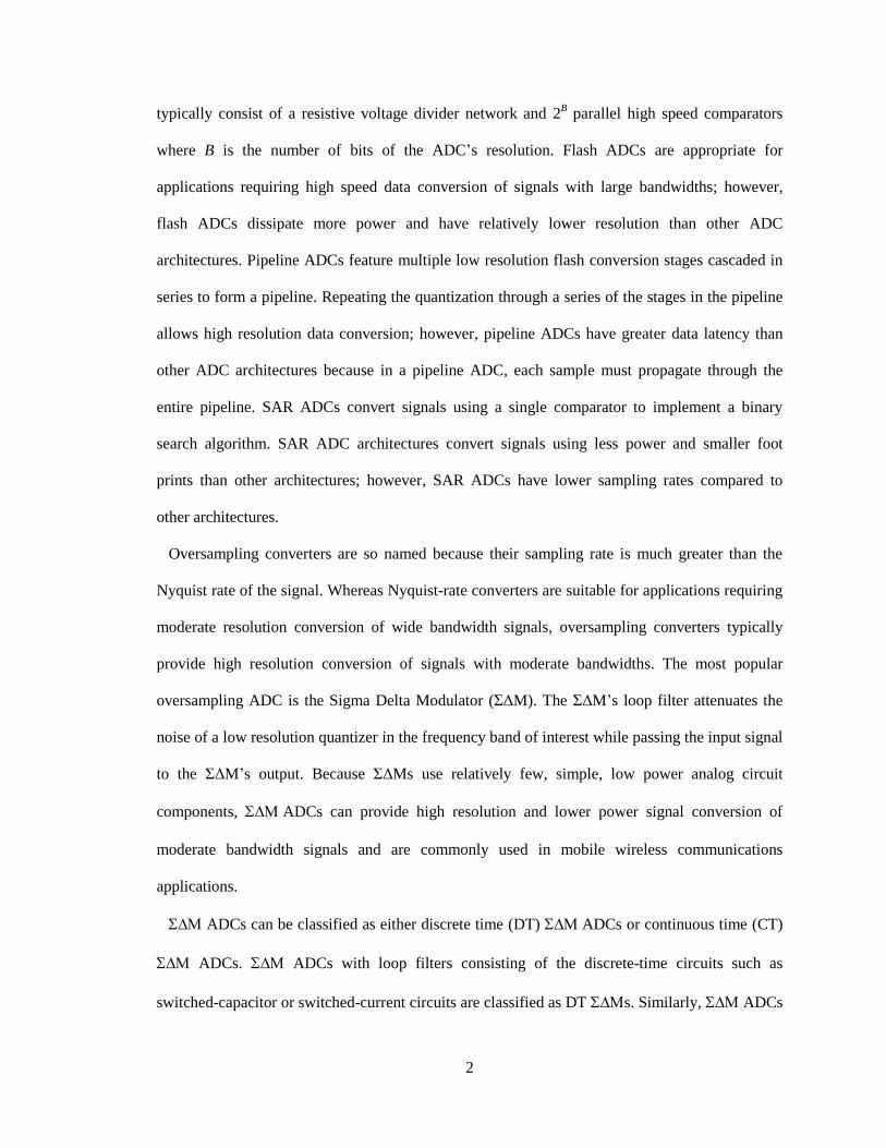
2
typically consist of a resistive voltage divider network and 2B parallel high speed comparators
where B is the number of bits of the ADC’s resolution. Flash ADCs are appropriate for
applications requiring high speed data conversion of signals with large bandwidths; however,
flash ADCs dissipate more power and have relatively lower resolution than other ADC
architectures. Pipeline ADCs feature multiple low resolution flash conversion stages cascaded in
series to form a pipeline. Repeating the quantization through a series of the stages in the pipeline
allows high resolution data conversion; however, pipeline ADCs have greater data latency than
other ADC architectures because in a pipeline ADC, each sample must propagate through the
entire pipeline. SAR ADCs convert signals using a single comparator to implement a binary
search algorithm. SAR ADC architectures convert signals using less power and smaller foot
prints than other architectures; however, SAR ADCs have lower sampling rates compared to
other architectures.
Oversampling converters are so named because their sampling rate is much greater than the
Nyquist rate of the signal. Whereas Nyquist-rate converters are suitable for applications requiring
moderate resolution conversion of wide bandwidth signals, oversampling converters typically
provide high resolution conversion of signals with moderate bandwidths. The most popular
oversampling ADC is the Sigma Delta Modulator (ΣΔM). The ΣΔM’s loop filter attenuates the
noise of a low resolution quantizer in the frequency band of interest while passing the input signal
to the ΣΔM’s output. Because ΣΔMs use relatively few, simple, low power analog circuit
components, ADCs can provide high resolution and lower power signal conversion of
moderate bandwidth signals and are commonly used in mobile wireless communications
applications.
ADCs can be classified as either discrete time (DT) ADCs or continuous time (CT)
ADCs. ADCs with loop filters consisting of the discrete-time circuits such as
switched-capacitor or switched-current circuits are classified as DT s. Similarly, ADCs

3
with the loop filters consisting of continuous-time circuits such as transconductors and integrators
are classified as CT s. Some of the advantages that CT ΣΔMs have over DT ΣΔMs are that
CT ΣΔMs have inherent antialiasing filtering in the ΣΔM’s signal transfer function (STF) and
they can operate at higher frequencies because they don’t have settling time requirements in their
loop filters [2]. Because DT ΣΔMs are simply made up of delays and gains, they can be
accurately modeled using simple difference equations whereas CT ΣΔMs can be more difficult to
simulate due to the mixed signal nature of the feedback loop.
Because mixed-signal integrated circuits such as CT ΣΔMs contain both analog and digital
circuits, mixed signal circuits are not as simple to model and simulate as all discrete or all analog
systems. Several common approaches for simulating CT ΣΔMs include SPICE modeling, solving
differential equations analytically and numerically, implementing difference equations based on
the impulse invariance transformation and using Simulink. Each simulation method has a tradeoff
between speed, simplicity and accuracy. In this dissertation, the delta transform is used to
simulate CT ΣΔMs, and its speed and accuracy are compared to the other methods.
This delta transform method simulates CT ΣΔΜs by determining difference equations that
model CT ΣΔΜs. The difference equations use the ΣΔΜ’s input signal and the quantizer’s
feedback signal to determine the input at the quantizer’s next sample time. However, unlike the
other difference equation methods, the delta transform can be used to determine all loop filter
signal values at times other than the sampling time. The delta transform has the particular
property that as the delta transform sample time approaches zero, the delta transform variable
converges toward its continuous time counterpart, the Laplace transform variable [3].
Because a ΣΔM’s output is typically the ΣΔM’s quantizer output which has a minimum and
maximum output, it is possible for the ΣΔM’s input to overload the ΣΔM’s quantizer. The ΣΔM’s
quantizer is said to be overloaded when the quantization error exceeds the quantizer’s minimum
and maximum values by more than half of one quantized level. When overloaded, a ΣΔM’s
output signal to quantization noise ratio (SQNR) decreases when the ΣΔM’s input is increased

4
over a certain value; however, in these cases, the ΣΔM’s output SQNR can be restored to its
previous values when the ΣΔM’s input is decreased to its previous amplitudes. In this dissertation,
the range of quantizer gains that cause overload are determined, and these values are used to
determine the input signal power that prevents overload.
Because a ΣΔM’s output is typically the ΣΔM’s quantizer output which has a minimum and
maximum output, ΣΔMs cannot be unstable in the bounded input bounded output (BIBO) sense.
Instead, a ΣΔM is considered to have become unstable when the amplitude of a ΣΔM’s input is
increased so as to cause the ΣΔM’s output SQNR to decrease dramatically and to create the
condition that the ΣΔM’s output SQNR cannot be restored to its previous values even when the
ΣΔM’s input is decreased to its previous amplitudes. DT root locus methods have been
successfully used to determine the stability of DT ΣΔMs; however, determining the stability
criteria for CT ΣΔMs is more difficult than it is for DT ΣΔMs because CT ΣΔMs include delays
which are modeled mathematically by exponential functions for CT systems. Because both the
STF and noise transfer function (NTF) of CT ΣΔMs contain exponential functions, traditional
root locus methods cannot be used for determining the root locus of CT ΣΔMs. Instead, in this
dissertation, an analytical root locus method is used to determine the stability criteria for CT
ΣΔMs. This root locus method determines the range of quantizer gains for which a CT ΣΔM is
stable. These values can then be used to determine input signal and internal signal powers that
prevent ΣΔMs from becoming unstable.
Using the analytical root locus stability analysis and the overload analysis, the SQNR of a CT
ΣΔM can be predicted. The quantization noise power is determined from the range of quantizer
gains that prevent ΣΔMs from becoming unstable or overloaded. The maximum input amplitude
to prevent ΣΔMs from becoming unstable or overloaded can be predicted using the range of
quantizer gains.
Chapter 2 in this dissertation reviews basic ADC and metrics and operation principles.
Also, the ΣΔM topologies that are used throughout this dissertation are developed using block
5
diagrams. In Chapter 3, a delta transform method for simulating CT ΣΔMs is developed. This
simulation method is compared with several existing CT ΣΔMs simulation methods with respect
to accuracy, speed and modeling simplicity. Chapter 4 states the necessary conditions that prevent
quantizers in CT ΣΔMs from overloading. Using these conditions, the maximum input signal
power that prevents a CT ΣΔM from overloading is determined. Also, a method is developed that
predicts a ΣΔM’s SQNR using the range of quantizer gains that prevent the ΣΔM from
overloading. In Chapter 5, an analytical root locus method is used to determine the stability
criteria for CT ΣΔMs that include exponential functions in their characteristic equations. This root
locus method determines the range of quantizer gains for which a CT ΣΔM is stable. These values
can then be used to determine input signal and internal signal powers that prevent ΣΔM from
becoming unstable. Finally, Chapter 6 summarizes the work presented.

6
CHAPTER 2
FUNDAMENTALS OF CT ΣΔM
Analog to digital conversion is a process that transforms analog signals which are continuous
in time and amplitude into digital signals which are discrete in time and amplitude. Although
this process can be implemented using a large variety of methods, the overall ADC process can
be modeled mathematically by three simple systems. From this model, a mathematical definition
of resolution can be defined so that the resolution of different ADC architectures can be
compared.
Although different architectures exist for CT ΣΔMs, most single quantizer CT ΣΔMs can be
described by a canonical feedback loop. This model allows CT ΣΔMs to be modeled
mathematically so that their resolutions can be determined without the need for developing
specific architectures. After developing a mathematical CT ΣΔM model that meets resolution
specifications, the model can then be mapped to a specific CT ΣΔM architecture and
implemented in hardware.
2.1 Performance of Analog to Digital Converters
The general ADC process can be modeled by three subsystems, an anti-aliasing filter (AAF), a
sampler, and a quantizer. Each of these subsystems has a simple mathematical model that can be
used to define general ADC metrics. An ADC’s resolution is one such metric, and it is often
defined in terms of effective number of bits (ENOB), SQNR, and dynamic range (DR).
2.1.1 Mathematical models of sampling and quantization
Fig 2.1 (a) shows a typical ADC process modeled by the three subsystems, an anti-aliasing
filter (AAF), a sampler, and a quantizer. In this model, the AAF filters the analog input signal,
x(t). The sampler converts the filtered signal, xa(t), into the discrete signal, x(n), such that x(n)

7
=xa(n∙Ts) where Ts is the sampling period. The third process, the quantizer, quantizes the
amplitude of x(n).
(a) (b) (c)
Figure 2.1 Operation principles of an ADC: (a) Block diagram of a classical analog to digital
converter, (b) Time domain example, (c) Frequency domain example[4]
Fig 2.1 (b) shows an example of this process in the time domain for a sinusoidal input signal,
and Fig 2.1 (c) shows an example of this process in frequency domain for a wideband signal. As
illustrated in Fig 2.1 (b) and (c), the AAF removes out of band frequency components which can
fold into the signal band during the subsequent sampling process. Ideally, the AAF is an ideal
(brick wall) lowpass filter (LPF) that has a cut-off frequency of fc which equals the maximum
bandwidth, fb, of the signal of interest. As shown in Fig 2.1 (c), the filtered signal, xa(t), only
contains frequency components between –fb and fb. The filtered signal, xa(t) must be sampled at a
8
minimum sampling rate, fs, of 2∙fb to prevent aliasing and consequently information loss. When
the sampler samples xa(t) with a period of Ts where Ts = 1/fs , the sampler generates the discrete
signal, x(n) where x(n) = xa(n∙Ts). As illustrated in Fig 2.1 (c), sampling xa(t) with a period of Ts =
1/2fb , generates a periodic extension of Sxa(t)(f) in the frequency domain as shown in the plot of
Sx(n)(f). The quantizer quantizes the amplitude of x(n) into the digital signal, y(n). In the time
domain, the quantizer generates an amplitude error between y(n) and x(n). This quantization error
between y(n) and x(n) depends on the quantization method (truncation or rounding) and the
number of equally spaced quantization levels. A B-bit quantizer has 2B equally spaced
quantization levels. In the frequency domain, quantization adds noise to Sx(n)(f). This noise limits
the ADC’s resolution.
(a) (b)
(c) (d)
Figure 2.2 (a) B-bit quantizer block, (b) Equivalent linear model of quantizer
(c) Probability density function of e(n), (d) Power spectral density of e(n)[5]
An ideal quantizer shown in Fig 2.2 (a) is often modeled linearly as a linear gain, K, and an
additive quantization noise, or error, e(n), as shown in Fig 2.2 (b); thus, a quantizer can be
modeled as y(n) = K∙x(n)+e(n) where y(n) is the quantizer’s output, x(n) is the quantizer’s input,
and e(n) is the quantizer error. The quantization error is generally modeled as a white random
9
process that has uniform distribution over the range of errors. Because the statistical mean for
rounding is zero unlike the statistical mean for truncation and because the statistical variance for
rounding is lower than it is for truncation, quantization is almost always performed by rounding
instead of truncation.
Rounding errors have a range of [-Δq/2, +Δq/2] where Δq is the quantization step size which is
defined as the difference between adjacent digital output levels. Rounding errors can be modeled
by a white random process that is uniformly distributed over the range of [-Δq/2, +Δq/2]. Because
the quantization error, e(n), is modeled as a uniformly distributed random process over the
interval, [-Δq/2, +Δq/2], the amplitude of the quantization noise’s probability density function,
P(e), is 1/ Δq as shown in Fig 2.2 (c). Because the quantization noise has zero mean, the total
quantization noise power, Pe, can be calculated as
2 2 2 2
2
2 22
2
( ) ( )
1 ( ) .
12
q
q
e e e
q
q
P E e E e
e P e de e de
(2.1)
Because the total quantization noise is modeled as a white random process that is uniformly
distributed over the frequency range of [-fs/2, fs/2], the quantization error’s power spectral density,
Se( f ), can be determined from
2/2
2
/2( ) ( )
12
s
s
fq
e e e sf
S f df S f f (2.2)
which implies that
2
( ) .12
q
e
s
S ff
(2.3)
2.1.2 Oversampling
The resolution of a B-bit ADC can be increased by a process called oversampling. If an ADC’s

10
sampling frequency, fs, exceeds twice the input signal’s bandwidth, fb, that is, fs > 2∙fb, a signal is
said to be oversampled and the ADC is said to be an oversampling ADC. An ADC’s
oversampling ratio (OSR) is defined as
2 s
b
fOSR
f (2.4)
To illustrate, an ADC operating with an OSR = 1 is a Nyquist rate ADC whereas an ADC
operating with an OSR = 2 is an oversampling ADC.
(a) (b) (c)
Figure 2.3 Power spectral density of the total quantization noise for (a) a Nyquist rate ADC,
(b) an oversampling ADC with OSR=2, (c) power spectral density of the quantization noise
power within signal bandwidth for an oversampling ADC with OSR=2
For both Nyquist rate converters and oversampling converters, the ADC’s quantization noise
power, 2
e ,
is 2 /12q . However, the output of an oversampling ADC can be filtered below –fb
and above fb which implies that after filtering, the quantization noise power can be reduced to
' '
' '
2
,
2 2/(2 ) /(2 )
'/(2 ) /(2 )
( )
1( ) .
12 12
b
b
s s
s s
f
e oversampling ADC ef
f OSR f OSRq q
ef OSR f OSR
s
S f df
S f df dff OSR
(2.5)
Fig 2.3 graphically illustrates this effect. Fig 2.3 (a) shows that the power spectral density (PSD)

11
of the quantization noise of a Nyquist rate ADC and Fig 2.3 (b) shows the PSD of the
quantization noise of an equivalent ADC that is operated with OSR = 2. As illustrated in Fig 2.3
(c), the power of the quantization noise can be reduced by 1/OSR by filtering out signals outside
the bandwidth of fb, or fs′/(2∙OSR). Because the quantization noise power,
2 , e of an oversampled
ADC is inversely proportional to the ADC’s OSR, an oversampling ADC’s SQNR increases as its
OSR increases.
2.1.3 Overload
Fig 2.4 shows the transfer characteristic for a typical B-bit quantizer with an input, x, and an
output, y. Assuming that the ADC’s maximum and minimum outputs are V and –V, respectively,
the difference, Δq, between two adjacent output levels can be written as
2
.2 1
q B
V
(2.6)
V
-V
x
y
≈ ≈
≈
≈
q
Figure 2.4 Transfer characteristic for a typical B-bit quantizer
When the quantizer’s output is at ±V and the magnitude of the quantizer’s error, e, exceeds half
of Δq, that is, when y =±V and
,2
qe
(2.7)

12
the ADC is said to be overloaded [6]. Therefore, for the an ADC with the transfer characteristic
in Fig 2.4, the ADC is not overload when
.2 2
q qV x V (2.8)
Using (2.6) and (2.8), the maximum input amplitude, xmax, of a B-bit quantizer in the non-
overload region is
max
2
2 2 1
Bq
Bx V V (2.9)
and the minimum input amplitude, xmin, of a B-bit quantizer in the non-overload region is
min
2 .
2 2 1
Bq
Bx V V (2.10)
2.1.4 Dynamic Range (DR)
The DR of an ADC is defined as the ratio between the power of the largest input signal that can
be applied without significantly degrading the performance of the ADC and the power of the
smallest detectable input signal at any frequency. The smallest detectable input signal is
determined by the PSD of the ADC’s noise floor. If the PSD of the noise floor is not uniform, the
smallest detectable signal is determined where the noise floor’s PSD is largest.
2.1.5 Signal to Quantization Noise Ratio (SQNR)
The SQNR of an ADC can be defined as the ratio of output signal power to quantization noise
power; that is,
y
e
PSQNR
P (2.11)
where Py is the ADC’s output signal power and Pe is the ADC’s output quantization noise power.

13
Assuming that the ADC’s output and quantization noise have zero means,
2 2[ ]y yP E y (2.12)
and
2 2[ ]e eP E e (2.13)
and an ADC’s SQNR in dB can written as
2
2( ) 10 log dB.
y
e
SQNR dB
(2.14)
For a full scale sinewave input, the output signal power, 2
y , can be calculated as
2 2 12 2max
2
2
2 (2 1)
B
y B
xV
(2.15)
where xmax is the maximum amplitude of the sinusoidal input signal. Substituting (2.2) into (2.6)
and the resulting equation into (2.14), the SQNR of a Nyquist rate ADC can be written as
( ) 1.76 6.02 Nyquist ADCSQNR dB B (2.16)
Eq. (2.16) shows that an ADC’s SQNR is proportional to the number of bits, B, of the ADC’s
resolution. In practice, (2.16) is used to calculate the ADC’s ENOB of resolution; that is,
( ) 1.76.
6.02
SQNR dBENOB (2.17)
Therefore, an ADC with a 6dB better SQNR has one additional bit of ENOB. This resolution
metric defined as ENOB gives an indication of how many bits would be required in an ideal ADC
to get the same performance.
The SQNR of an oversampled ADC can be calculated by substituting (2.5) and (2.15) into
(2.14), which results in
14
( ) 1.76 6.02 10 log( ). oversampling ADCSQNR dB B OSR (2.18)
Eq. (2.18) shows that doubling an ADC’s OSR increases its SQNR by 3dB. For example, an
ADC with an OSR of 4 will have a 6dB better SQNR than the same ADC operated at the Nyquist
rate. As a result, an ADC’s ENOB can be increased by 1 bit by sampling the signal 4 times faster
than its Nyquist rate.
2.2 The Operation Principles of Sigma Delta Modulators
ΣΔM ADCs achieve a high resolution signal conversion by using a feedback loop filter and a
low resolution quantizer that samples at rates much higher than the Nyquist rate. The loop filter
is designed not only to shape the quantization noise so that it is attenuated over the frequency
band of interest, but also to act as an AAF for the input signal. This is known as the “noise
shaping technique”.
In a general, a CT ΣΔM can be modeled by the canonical feedback loop shown in Fig 2.5 (a)
where X(s) and Y(s) are the Laplace transforms of the input signal and the output signal,
respectively, and F(s), G(s) and H(s) are the system functions of the pre-filter stage, the
feedforward path and the feedback path, respectively. The continuous to discrete (C/D) block
converts a continuous time signal into a discrete time signal. The C/D converter can be modeled
by an impulse train modulator, followed by a block that converts the impulse train into a discrete
time sequence [7]. Because the discrete time Fourier transform of the output of the C/D converter
is identical to the Fourier transform of the input of the C/D converter if the input of C/D converter
is bandlimited and oversampled, the system function of the C/D converter doesn’t need to be
included in the model. The quantizer block represents a clocked quantizer, and the DAC block
represents a digital to analog converter (DAC). The quantizer delay and the DAC delay are often
represented by a single delay block as they are in Fig 2.5 (a), and the combination of these two
delays is often referred to as the ΣΔM’s excess loop delay.

15
(a)
(b)
(c)
Figure 2.5 (a) Block diagram of a CT ΣΔM, (b) A linear model for the CT ΣΔM’s STF,
(c) A linear model for the CT ΣΔM’s NTF
Fig 2.5 (b) shows a linear model for the CT ΣΔM’s STF where the quantizer has been
modeled by the variable gain, K. Fig 2.5 (c) shows a linear model for the CT ΣΔM’s NTF where
the quantization error is modeled by the gain, K, and an additive quantization noise, E(s). Because
the block diagram models in Fig 2.5 (b) and (c) are linear, the ΣΔM’s output, Y(s) can be written
as
( ) ( ) ( ) ( ) ( ) Y s STF s X s NTF s E s (2.19)
where

16
( ) ( ) / ( ) ,STF s Y s X s and ( ) ( ) / ( ) .NTF s Y s E s (2.20)
Using Fig 2.5 (b), the ΣΔM’s STF can be written as
( ) ( )
,1 ( ) (
( )) ( )sD
K F s G s
K e G s H sS s
sT
DACF
(2.21)
and using Fig 2.5(c), the ΣΔM’s NTF can be written as
( )1
1 ( ) ( ) ( )sDK e G s H s DAC sNTF s
(2.22)
where the exponential function, e-sD
is the Laplace transform of the excess loop delay, D.
In general, stable feedback loops minimize feedback error. Therefore, when calculating the
output signal power, ,yP of the ΣΔM, the value of K is selected as the ΣΔM’s effective gain, Keff,
which is the value of K that minimizes the power, ,eP of the quantization noise [8]. Because
( ) ,e n y K the ΣΔM’s quantization noise power, ,eP can be written as
2 2 2 2[ ( )] [ ( )] 2 [ ( ) ( )] [ ( )].eP E e n E y n K E y n n K E n (2.23)
The necessary condition for K to minimize eP is
22 [ ( ) ( )] 2 [ ( )] 0eeff
PE y n n K E n
K
(2.24)
which implies that the Keff that minimizes eP is
2
[ ( ) ( )].
[ ( )]eff
E y n nK
E n
(2.25)
Assuming ( )n is a zero mean random process and assuming a single bit quantizer which
implies ( ) sgn[ ( )],y n n (2.25) can be written as

17
2
[ ( ) ].eff
E nK
(2.26)
To illustrate the operation of a ΣΔM, consider a NTF that is designed as a highpass Chebyshev
Type 2 filter and a STF that has the lowpass characteristic shown in Fig 2.6. For low frequiencies,
the magnitude response of the NTF is almost zero, that is, ( ) 0NTF j for 72 10 , so the
quantization noise will be attenuated in that part of output spectrum. Also, for low frequencies,
the magnitude response of the STF is approximately one which implies that the input signal is
passed to the output without attenuation. However, for high frequencies, the NTF passes the
quantization errors with a gain of one and the STF attenuates the input signal to reduce aliasing.
Figure 2.6 STF/NTF magnitude response designed with the Chebyshev2 filter
Fig 2.7 (a) shows an example of an input signal and the uniformly distributed quantization
noise generated by the quantizer. Fig 2.7 (b) shows the output spectra of those signals after they
have been filtering by the STF and the NTF, respectively. Because the spectrum of the
quantization noise is shaped by the NTF, significant reduction of in-band quantization noise and
improvement in SQNR occur.
18
(a)
(b)
Figure 2.7 The spectra of the input signal and the quantization noise
(a) before the noise shaping, (b) after the noise shaping
19
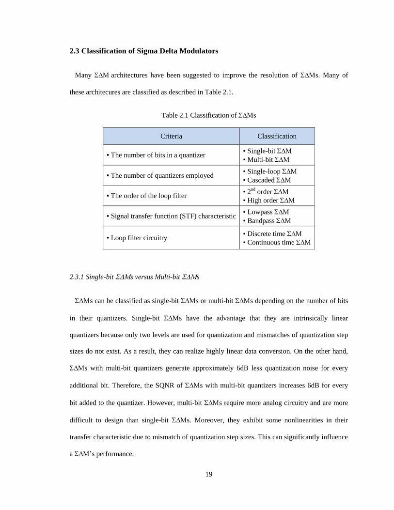
2.3 Classification of Sigma Delta Modulators
Many architectures have been suggested to improve the resolution of s. Many of
these architecures are classified as described in Table 2.1.
Table 2.1 Classification of s
Criteria Classification
▪ The number of bits in a quantizer ▪ Single-bit
▪ Multi-bit
▪ The number of quantizers employed ▪ Single-loop
▪ Cascaded
▪ The order of the loop filter ▪ 2
nd order
▪ High order
▪ Signal transfer function (STF) characteristic ▪ Lowpass
▪ Bandpass
▪ Loop filter circuitry ▪ Discrete time
▪ Continuous time
2.3.1 Single-bit s versus Multi-bit s
s can be classified as single-bit s or multi-bit s depending on the number of bits
in their quantizers. Single-bit s have the advantage that they are intrinsically linear
quantizers because only two levels are used for quantization and mismatches of quantization step
sizes do not exist. As a result, they can realize highly linear data conversion. On the other hand,
s with multi-bit quantizers generate approximately 6dB less quantization noise for every
additional bit. Therefore, the SQNR of s with multi-bit quantizers increases 6dB for every
bit added to the quantizer. However, multi-bit s require more analog circuitry and are more
difficult to design than single-bit s. Moreover, they exhibit some nonlinearities in their
transfer characteristic due to mismatch of quantization step sizes. This can significantly influence
a ’s performance.

20
2.3.2 Single-loop s versus Cascaded s
s employing only one quantizer are called single-loop s, whereas those employing
several quantizers are often named Cascaded sor MASH sCascaded topologies use
two or more low order s which are relatively stable and can achieve performances equivalent
to higher order single loop architectures which can suffer from potential instability. However, the
Cascaded topologies require tighter constraints on circuit specifications and mismatch than
single- loop s [8].
2.3.3 2nd order s versus High orders
s can be categorized as 2nd order s or high order s. If the order of a ’s loop
filter is greater than 2, the is called a high order . As the order of the loop filter
increases, the quantization noise can be suppressed more at low frequencies and a significant
improvement in performance can be achieved. However, high order s are conditionally
stable whereas 2nd order s can be designed to always be stable.
2.3.4 Lowpass s versus Bandpass s
Depending on a ’s NTF and STF characteristics, a can be classified as either a
lowpass (LP) or a bandpass (BP) . s that have NTFs with highpass shapes and
that have STFs with lowpass shapes are considered LP s. s that have NTFs with
bandstop shapes and that have STFs with bandpass shapes are called BP s.
2.3.5 Discrete Time s versus Continuous Time s
Finally, s can be classified as either discrete time (DT) s or continuous time (CT)
s. s with a loop filter consisting of discrete time circuits such as switched capacitor or

21
switched current circuits are called DT s. Similarly, s with a loop filter consisting of
continuous time circuits such as transconductors and integrators are called CT s.
2.3.6 s in this dissertation
Whereas DT ΣΔMs can be accurately simulated and analyzed using simple difference equations,
CT ΣΔMs are more difficult to simulate and analyze due to the mixed signal nature of the
feedback loop. Single loop, single-bit s have the advantage of being able to perform highly
linear data conversion; however, they can become unstable for loop filter orders higher than two.
In this dissertation, a stability criterion is developed for single loop CTs. This method is
illustrated using single loop, single-bit s with loop filter orders ranging from 2 to 5. An
overload criterion is also developed for single loop CTs. This method is also illustrated
using single loop, single-bit s with loop filter orders ranging from 2 to 5. Also, CTs
from 2nd order to 5th order are considered for comparison of simulation methods for CTs.
2.4 Topology Selection of the CT ΣΔM for simulations
After determining a desired NTF and STF, the NTF and STF coefficients need to be
implemented in a hardware structure, such as a cascade of resonators feedback (CRFB), cascade
of resonators feedforward (CRFF), cascade of integrator feedback (CIFB), and cascade of
integrator feedforward (CIFF) implementations. Each of these feedback architectures feeds back
the modulator output to each integrator. Because the amplifier nonlinearities generate harmonic
distortion that depends on the input signal of the amplifier, single loop feedback architectures
have signal distortion [9, 10, 11]. On the other hand, feedforward architectures sum all integrator
outputs and the input signal at the input of the quantizer. These architectures have the benefit of
lower signal distortion than feedback architectures. However, feedforward architectures require
extra components for the summation before the quantizer, and thus these architectures have a
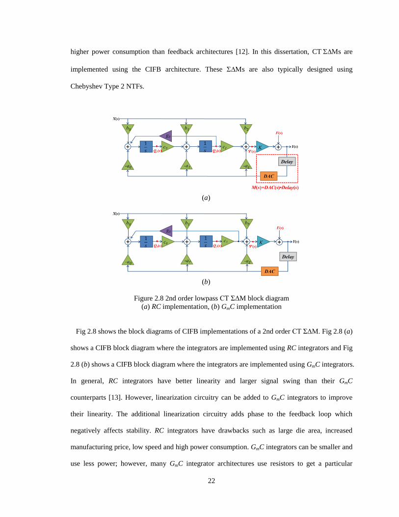
22
higher power consumption than feedback architectures [12]. In this dissertation, CTs are
implemented using the CIFB architecture. These s are also typically designed using
Chebyshev Type 2 NTFs.
(a)
(b)
Figure 2.8 2nd order lowpass CT ΣΔM block diagram
(a) RC implementation, (b) GmC implementation
Fig 2.8 shows the block diagrams of CIFB implementations of a 2nd order CT ΣΔM. Fig 2.8 (a)
shows a CIFB block diagram where the integrators are implemented using RC integrators and Fig
2.8 (b) shows a CIFB block diagram where the integrators are implemented using GmC integrators.
In general, RC integrators have better linearity and larger signal swing than their GmC
counterparts [13]. However, linearization circuitry can be added to GmC integrators to improve
their linearity. The additional linearization circuitry adds phase to the feedback loop which
negatively affects stability. RC integrators have drawbacks such as large die area, increased
manufacturing price, low speed and high power consumption. GmC integrators can be smaller and
use less power; however, many GmC integrator architectures use resistors to get a particular

23
transconductance, Gm, and the layout of these resistors can increase the GmC integrator’s die size
significantly.
From inspection of the block diagram shown in Fig 2.8 (a), the ΣΔM’s states, Q1(s) and Q2(s),
the quantizer’s input, Ѱ(s), and the ΣΔM’s output, Y(s) can be calculated as
1 0 0 0 2(1
( ) { ( ) ( ) )}) (M sQ s b X ss
a Y s g Q s (2.27)
12 1 0 1
1( ( ) { ( ) ( ) )}) (M sQ s b X s a Y s c Q s
s
(2.28)
2 2 1 2( )( ) ( ) ( ) ( )s b X s a Y s c Q sM s
(2.29)
and
( ) ( ) ( )Y s K s E s
(2.30)
where M(s) = DAC(s)·Delay(s). Substituting (2.27) into (2.28) and solving for Q2(s), the resulting
equation can be substituted into (2.29). Substituting that result into (2.30), the STF and the NTF
for the RC implementation in Fig 2.8 (a) can be determined to be
2
2 1 1 0 0 1 0 2 0
2
2 1 1 0 0 1 0 2 0 0 0
( )
1 ( ) ( ) ((
()
))
K b s b c s b c c g b c
K M s a s K M s a c s K M s a c c gSTF
as
c g c
(2.31)
and
2
0 0
2
2 1 1 0 0 1 0 2 0 0 0
.1 (
( ))) ( ) ( ) (
s g c
K M s a s K M s a c s K M s a c c g a c g cNTF s
(2.32)
The gains, a0, a1, a2, b0, b1, b2, c0, c1 and g0 can be determined by equating the STF coefficients in
(2.31) and the NTF coefficients in (2.32) with the desired STF and NTF coefficients, respectively.
Similarly, for the topology with the GmC implementation shown in Fig. 2.8 (b), the ΣΔM’s
states, Q1(s) and Q2(s), the quantizer’s input, Ѱ(s), and the ΣΔM’s output, Y(s) can be calculated

24
as
1 0 0 0 21
1 ( ) { ( ) ) ( ) ( )}(M sQ s b X s a Y s g Q sc
s (2.33)
12 1 0 1
1( ( ) { ( ) ( ) )}) (M sQ s b X s a Y s c Q s
s
(2.34)
2 2 1 2( )( ) ( ) ( ) ( )s b X s a Y s c Q sM s
(2.35)
and
( ) ( ) ( )Y s K s E s
(2.36)
where M(s) = DAC(s)·Delay(s). Substituting (2.33) into (2.34) and solving for Q2(s), the resulting
equation can be substituted into (2.35). Substituting that result into (2.36), the STF and the NTF
for the GmC implementation shown in Fig 2.8 (b) can be determined to be
2
2 1 1 0 0 1 0 2 0 1
2
2 1 1 0 0 1 0 2 0 0 01 1
( )
1 ( ) (( )
)) ( ) (
K b s b c s b c c g b c c
K M s a s K M s a c s K M s a c cSTF s
ca g ccg c
(2.37)
and
2
0 0 1
2
2 1 1 0 0 1 0 2 0 1 0 0 1
.1
((
)) ( ( ) )) (
s g c c
K M s a s K M s a c s K M s a c c g a c c g c cNTF s
(2.38)
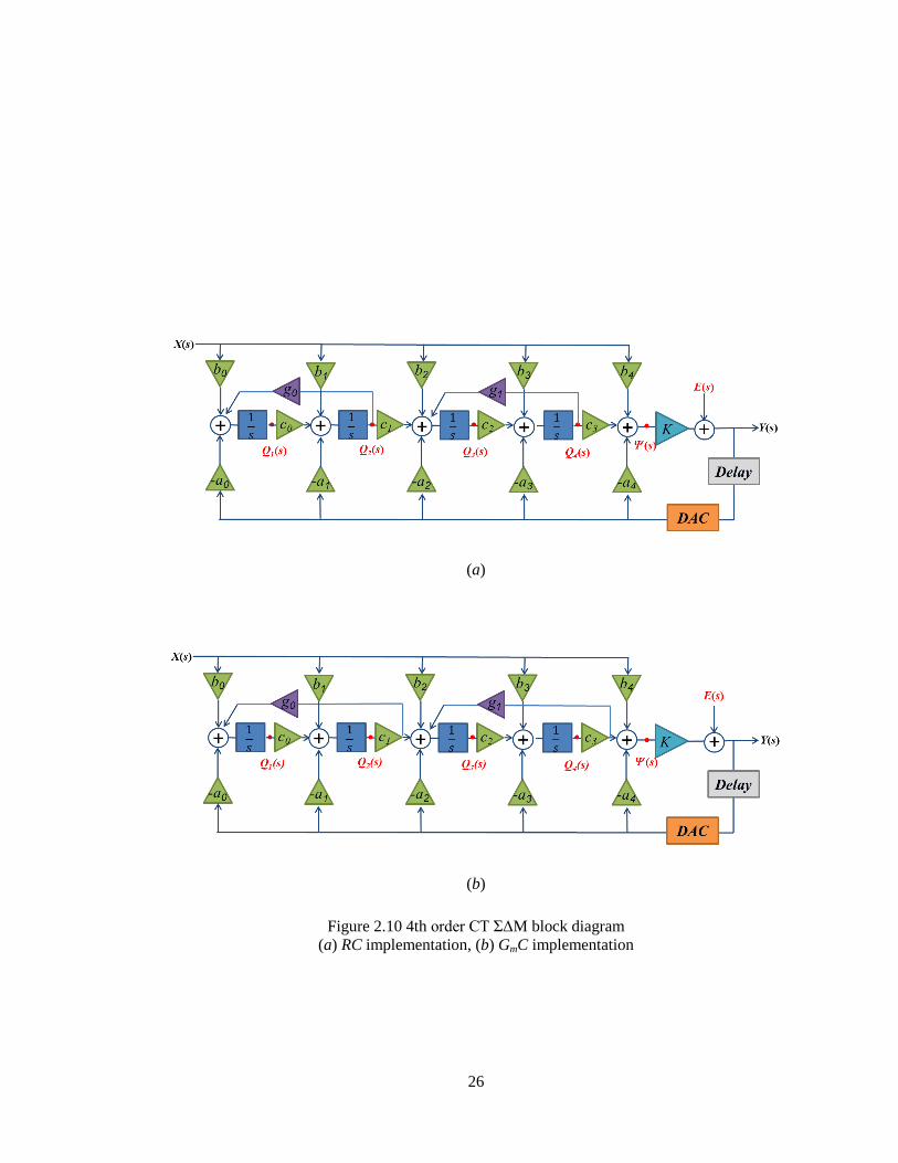
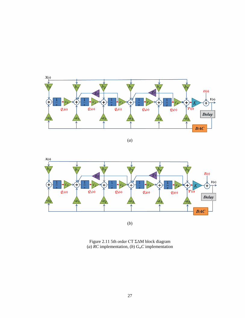
Fig 2.9, Fig 2.10, and Fig 2.11 show the block diagrams of CIFB implementations of 3rd order,
4th order, and 5th order CT ΣΔMs, respectively. Using techniques similar to the ones used to
determine the STF and NTF of the 2nd order CIFB implementations, the STFs and NTFs for the
CIFB implementations of the 3rd order through 5th order CT ΣΔMs can be determined as shown
in Table 2.2 and Table 2.3. Table 2.2 shows the STF and NTF coefficients for the RC
implementations and Table 2.3 shows the STF and NTF coefficients for the GmC implementations.

25
2.5 Conclusion
In this Chapter, the general ADC process was modeled mathematically, and from this model,
SQNR, DR, and ENOB were defined. It was also shown that ΣΔM ADCs achieve a high
resolution signal conversion by using an oversampling quantizer and a feedback loop filter.
Various ΣΔM architectures can be used to implement CT ΣΔMs. For this dissertation, single
loop, single-bit CT ΣΔMs with loop filter orders ranging from 2 to 5 are implemented using the
CIFB architecture.
(a)
(b)
Figure 2.9 3rd order CT ΣΔM block diagram
(a) RC implementation, (b) GmC implementation
26
(a)
(b)
Figure 2.10 4th order CT ΣΔM block diagram
(a) RC implementation, (b) GmC implementation
27
(a)
(b)
Figure 2.11 5th order CT ΣΔM block diagram
(a) RC implementation, (b) GmC implementation

28
Tab
le 2.2
CT
ΣΔ
M S
TF
and N
TF
coefficien
ts for R
C im
plem
entatio
ns

29
Tab
le 2.3
CT
ΣΔ
M S
TF
and N
TF
coefficien
ts for G
mC
implem
entatio
ns
30
CHAPTER 3
A COMPARISON OF CT ΣΔM SIMULATION METHODS
Because DT ΣΔMs are simply made up of delays and gains, they can be accurately modeled
using simple difference equations. On the other hand, CT ΣΔMs can be more difficult to simulate
due to the mixed signal nature of the feedback loop. Several common approaches for simulating
CT ΣΔMs have been developed and the representative methods include SPICE modeling, solving
differential equations analytically and numerically, implementing difference equations based on
impulse invariance transform and using Simulink. Each simulation method has a tradeoff between
simplicity, speed and accuracy. In this chapter, the delta transform is used to determine difference
equations that model CT ΣΔMs. These difference equations use the ΣΔΜ’s input signal and the
quantizer’s feedback signal to determine the input at the quantizer’s next sample time. However,
unlike the other difference equation methods, the delta transform can be used to determine the
loop filter signal values at times other than the sampling time. This method’s modeling simplicity,
accuracy and speed are compared to existing simulation methods by simulating several CT ΣΔΜs.
3.1 The Conventional Approaches to Simulating CT ΣΔΜs
CT s are most commonly simulated by using SPICE, solving differential equations,
implementing difference equation based on the impulse invariance transform, and using
Simulink/MATLAB.
3.1.1 Macromodel in SPICE
Simulating CT ΣΔΜs using SPICE usually begins with macro level simulations using ideal
components such as ideal voltage controlled voltage, or current, sources and ideal quantizers.
These simulations are typically used to determine the ΣΔΜ’s ideal performance. After the macro
model has been designed to meet performance specifications, specific transistor level systems,

31
such as operational amplifiers, transconductance amplifiers, and DACs can be substituted for the
macro level components to observe nonideal effects such as finite amplifier gains and bandwidths,
parasitic capacitances and quantizer metastability. Full circuit level simulation using SPICE can
usually be expected to give realistic results because transistor level models include nonideal
effects such as finite transistor gains, finite amplifier bandwidths, and parasitic capacitances.
(a)
(b) (c)
Figure 3.1 Macromodel of a 2nd order CT ΔΣM[15]
(a) Functional blocks of a 2nd order CT ΣΔM, (b) RC integrators implementation
for a loop filter, (c) GmC integrators implementation for a loop filter
As shown in Fig 3.1 (a), a CT ΔΣM can be divided into functional blocks which can be further
divided into individual circuits and sub-circuits. A loop filter can be implemented using RC

32
integrators or GmC integrators. Fig 3.1 (b) shows an RC integrator macro model circuit for the
integrators in Fig 3.1 (a). Fig 3.1 (c) shows a GmC integrator macro model circuit for the
integrators in Fig 3.1 (a). SPICE simulation can generate the most accurate simulation results
because the nonideal effects can be reflected in the circuit. However, simulating CT ΣΔΜs using
SPICE can be time consuming even for macro models, and they are especially time consuming
for higher order ΣΔΜs [15].
3.1.2 Solving differential equations
Figure 3.2 Circuit model of a 2nd order CT ΣΔM[4]
Alternatively, the simulation of the 2nd order CT ΔΣM shown in Fig 3.1 can be approached by
using the equivalent circuit depicted in Fig 3.2. A set of differential equations can be determined
by writing the circuit’s node equations. To illustrate, consider the single-ended circuit model of a
2nd order CT ΔΣM shown in Fig 3.2 [17]. By applying Kirchhoff’s current law (KCL) to the
nodes, v1 and v2,
1 1 1 1 1 1 1
1
1( )( ) ( ) ( ) ( )m i
i
g a y n sC v sC vt t tR
x t q
(3.1)
1 22 22 2 22
2
1( ) ( ) ( ) ( )( )m i
i
g q t ta y n sC v s tC vR
q t
(3.2)

33
where
11
1
( )( )
q tv t
A
,
22
2
( )( )
q tv t
A
In the time domain, (3.1) and (3.2) can be written as
11 1
1 1 1
1 1 1
1
( )(
())
)(
1
m
i
i
qg a y n
dq R A
dtC
t
A
x tt
C C
(3.3)
and
22 2
2 2 2
1
2 2 2
2
( )( ( ))
,( )
1
m
i
i
qg a y n
dq R A
dtC C C
A
tq t
t (3.4)
respectively. This set of node equations can be written as linear state space equations and solved
numerically to determine the system behavior as a function of time [16, 17, 18]. The node
voltages, q1(t) and q2(t), which are the solution of the differential equations are composed of a
zero input response (ZIR) which is a function of the initial condition, and a zero state response
(ZSR) which is a function of the input, x(t). A ZIR and a ZSR can be obtained using the resolvent
matrix of the system [16, 17, 18].
This approach to modeling and simulating CT ΔΣMs allows nonideal effects such as finite
amplifier gain (such as A1 or A2) and finite amplifier bandwidth to simply be added to the model
and simulation. While this method can simulate a ΣΔΜ much faster than using SPICE, it is not as
fast or as simple as other methods.
3.1.3 Implementing difference equation (CT/DT equivalence)
Two other ΣΔΜ simulation approaches use difference equations to model the ΣΔΜ’s loop filter.
These difference equations use the ΣΔΜ’s input signal and the quantizer’s feedback signal to
determine the input at the quantizer’s next sample time . This method then iterates these

34
calculations for each clock sample.
Figure 3.3 Equivalence between a CT ΣΔM and a DT ΣΔM
One of these methods determines the difference equations using the impulse invariance
transformation. Fig 3.3 indicates that the equivalence between a CT ΣΔΜ and a DT ΣΔΜ for both
ΣΔΜs to have identical outputs. The quantizer inputs of both of the CT ΣΔΜ and the DT ΣΔΜ
must be identical at sampling instants, n∙TS where n is the sample number and TS is sampling
period. This requires that the impulse responses of the CT ΣΔΜ and the DT ΣΔΜ are identical at
the sampling instants, leading to the condition
1 1 |
t n TsDACG z s G s (3.5)
or, in the time domain,
= ( ) ( )* (( ) ( ))
t n Tst n Ts
dan dac t g t c t g t d (3.6)

35
where dac(t) is the impulse response of the DAC and g(t) is the impulse response of the G(s)
block. The transformation between the CT and DT impulse responses is called the impulse-
invariance transformation [19]. This approach is much faster than SPICE simulation or solving
the differential equations; however, it can be less accurate than SPICE simulations.
The other difference equation method uses a short SPICE transient simulation and numerically
determines a difference equation that minimizes a 2 norm error between the SPICE data and the
difference equation output. Although this method is faster than SPICE simulations and the
differential equations method mentioned earlier, this method can be less accurate due to some
guesswork to find the best difference equations.
3.1.4 MATLAB/Simulink
Figure 3.4 Simulink model for a 2nd order CT ΣΔΜ
MATLAB/Simulink is also commonly used to simulate CT ΣΔΜs. Fig 3.4 show a Simulink
schematic of a 2nd order ΣΔΜ. Simulink schematics are quick and simple to create and
Simulink’s simulation times are relatively fast; however, Simulink’s simulation accuracy is often
dependent on the proper selection of Simulink models [20].

36
3.2 Simulating CT ΣΔΜs Using the Delta Operator
In this section, the delta transform is used to determine difference equations that model CT
ΣΔΜs. These difference equations use the ΣΔΜ’s input signal and the quantizer’s feedback signal
to determine the input at the quantizer’s next sample time. However, unlike the other difference
equation methods, the delta transform calculates the loop filter signal values at times between the
sampling times.
Because discrete systems are suitable for computer realization and continuous systems are not
and because continuous systems are often described in the Laplace transform’s s domain and
discrete systems are often described in the - transform’s z domain, many transformations have
been developed between the Laplace transform’s s domain and the - transform’s z domain [21].
One such transformation is the delta transform or delta operator [22]. The discrete delta operator
approximates the Euler derivative, and as the delta operator’s sampling period is reduced, not
only does the approximation improve, but the delta transform approaches the Laplace transform.
As a result, the delta transform’s poles and zeros, or the discrete system’s poles and zeros,
approach the Laplace transform’s poles and zeros, or the continuous system’s poles and zeros as
the delta transform sample period approaches. Thus, unlike many other discrete models, a delta
transform’s discrete model of a continuous system can better represent an underlying continuous
physical model by simply increasing the delta transform’s sampling rate.
3.2.1 Definition of Delta Transform
The delta transform, Δ, of a function f(t) is defined as
0
( ) ( )(1 )
n
n
f t T f n T T (3.7)
where is a complex variable and T is the transform’s sampling period. To show that
{f(t)}={f(t)}, where is the Laplace transform, as T approaches zero, consider

37
0
00
( ) ( ) lim ( ) .
st sn t
tnt
f t f t e dt f n t e t (3.8)
Letting T= Δt, and replacing esT
by its power series expansion, (3.8) can be written as
2
00
( )( ) lim ( ) 1 ( ) .
2!
n
Tn
s Tf t T f n T s T (3.9)
Without the limit, T → 0, (3.9) can be approximated as
1
0
( ) ( )(1 ) ( )
n
z Tn
f t T f n T T T f n T (3.10)
where ( )f n T is - transform of ( )f n T and is a complex variable where s as
0. T
To develop a transformation between the Laplace transform’s s domain, the delta transform’s δ
domain and the - transform’s z domain, consider Euler’s forward difference equation that
approximates the differential operator; that is, consider
( 1) ( )( ) .
t n T
f n T f n Tdf t
dt T (3.11)
Because the delta transform approaches the Laplace transform and → s as T → 0, (3.11)
implies that
0
( 1) ( )( ) ( )lim
T
t n T t n T
f n T f n Tdf t df t
dt dt T (3.12)
and therefore as T → 0,
1F( ) F( ) F( ) .
zs s z
T (3.13)
Thus, the delta transform implies that

38
1
1
1 1 .
1
T z
s z (3.14)
The transformation in (3.14) can be illustrated by the block diagrams in Fig 3.5.
Figure 3.5 Delta operator block diagram
As illustrated in (3.14), the relationship between the delta transform and the -transform is z =
1+𝛿∙TΔ. Because stability for the -transform requires that all the system’s poles lie within the
region, |z| < 1, stability for the delta transform requires all the system’s poles lie within the region,
|1+𝛿∙TΔ | < 1 which defines a circle of radius, 1/TΔ, centered at -1/TΔ. Therefore, as the sampling
time, TΔ approaches zero, the stability region of the delta transform becomes equivalent to that of
the Laplace transform whereas the stable region of the -transform is fixed to the interior of the
unit circle. Fig 3.6 shows a comparison of stability regions for the -transform, delta-transform,
and Laplace domain. These plots illustrate the mapping between the continuous and discrete
planes. It can be seen that as TΔ approaches zero, the stability region for the delta transform will
grow to approach that of the Laplace domain which is the whole left hand plane.
In summary, the delta-transform has the particular property that as the sample time, TΔ,
approaches zero, the delta-transform converges toward its continuous counterpart, the Laplace

39
transform. As a result, the delta-transform has superior performance at high sample rates
compared to the -transform because the continuous and discrete time models approach
equivalence when the delta transform has a small sampling time.
Figure 3.6 Stability regions for the continuous Laplace plane, and the discrete z-plane, delta-plane
3.2.2 Application of Delta Transform for CT ΣΔΜs simulation
Figure 3.7 The 2nd order CT ΣΔM block diagram
To apply the delta transform to the block diagram of a CT ΣΔM, consider the block diagram of
the CIFB implementation of a 2nd order CT ΣΔM described in Chapter 2 and shown in Fig 3.7.

40
The block diagram in Fig 3.7 describes a 2nd order CT ΣΔM where the ΣΔM’s STF and NTF are
given by
2
2 1 1 0 0 1 0 2 0
2
2 1 1 0 0 1 0 2 0 0 0
( )( )
1 ( ) ( ) ( ) )(
K b s b c s b c c g b c
K M s a s K M s a c s K M sST
a c c g a c g cF s (3.15)
2
0 0
2
2 1 1 0 0 1 0 2 0 0 0
1 ( ) ( ( )
()
))(
s g c
K M s a s K M s a c s K M s a c c g a cTF
cN s
g
(3.16)
To determine the coefficients in (3.15) and (3.16), a desired NTF is designed and set equal to the
NTF in (3.16). Throughout this dissertation, K is set equal to one unless otherwise noted. After
determining the NTF, the numerator of a desired STF is determined and set equal to the STF in
(3.15). In this dissertation, NTFs are designed as a highpass Chebyshev Type 2 filter with a cutoff
frequency near the ΣΔM’s bandwidth. STFs are designed as a lowpass filter using the poles of the
NTFs and the numerator of a lowpass Chebyshev Type 2 filter. The following MATLAB code
shows an example of such a ΣΔM that has a bandwidth of 20MHz and a sampling rate of 1GHz.
[NTFnum,NTFden]=cheby2(2,37,2*pi*22e6,'high','s');
NTF=tf(NTFnum,NTFden);
[STFnum,STFden]=cheby2(2,40,2*pi*750e6,'s');
STFnum=STFnum/STFnum(end)*NTFden(end);
STF=tf(STFnum,NTFden);
This code produces
2 17
2 9 17
0.01523 6.764 10( )
1.155 10 6.764 10
sSTF s
s s
(3.17)
and
2 -7 15
2 9 17
2.384 10 9.554 10
1.155(
10 6.764 10)NT
s
s ss
sF
(3.18)
The gains, a0, a1, a2, b0, b1, b2, c0, c1 and g0 in (3.15) and (3.16) can be determined by equating the

41
STF in (3.15) with the desired STF coefficients in (3.17) and by equating the NTF in (3.16) with
the desired NTF coefficients in (3.18), respectively.
To simulate the resulting ΣΔM, the integrators in Fig 3.7 are replaced by the expression in (3.14)
where the sampling rate, TΔ, is chosen to be less than the sampling rate, T, of the ΣΔM. Fig. 3.8
shows a block diagram of the CT ΣΔM represented in Fig 3.7 where the integrators have been
replaced by the delta transform equivalents.
Figure 3.8 2nd order DT model ΣΔM using delta transform
By inspection of the block diagram in Fig. 3.8, the difference equations describing the states can
be determined as
( ) ( ) dacy n DAC y n Delay (3.19)
1 0 0 0 2( ) dacq dot n b x n a y n g q n (3.20)
1 1 11 ( 1) q n T q dot n q n
(3.21)
12 1 0 1( ) dacq dot n b x n a y n c q n (3.22)
2 2 21 ( 1) q n T q dot n q n
(3.23)
2 2 1 2() )( dacb x n a y n c q nn (3.24)
if = / ,n T T
42
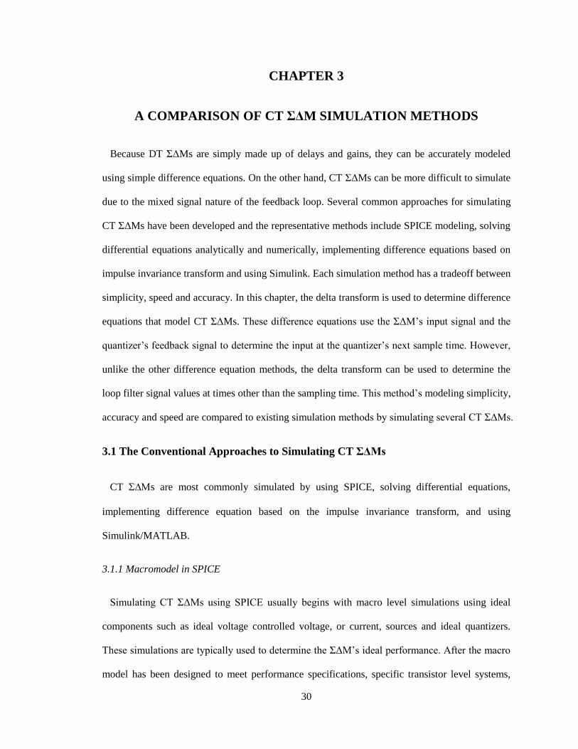
( ) sgn ( )y n n (3.25)
where DAC is a function that maps y(n-Delay) to a DAC output. This can be implemented in
Matlab using the following code:
% Analysis of 2nd Order sigma delta modulator(RC implementation)
for n = start:finish,
% First state
qdot(n,1) = b0*x(n) - a0*ydac(n-1) + g0*q(n-1,2);
q(n,1) = Delta*qdot(n,1) + q(n-1,1);
% Second state
qdot(n,2) = b1*x(n) - a1*ydac(n-1) + c0*q(n,1);
q(n,2) = Delta*qdot(n,2) + q(n-1,2);
% Input to quantizer
et(n) = b2*x(n) + c1*q(n,2) - a2*ydac(n-1);
% Quantizer
yq(n) = sign(et(n));
% DAC
y(n)=y(n-1);
if rem(n,DeltaOSR) == 0, % Update quantizers every Delta samples
y(n) = yq(n);
end
ydac(n) = y(n-D); % excess loop delay between quantizer and DAC
end
As TΔ decreases, this model converges towards its continuous counterpart and the simulation
results converge towards a simulation based on the differential equations describing the ΣΔM.
Also, because this discrete model uses difference equations, it can simulate more quickly than a
continuous time domain model. The delta transform can be easily applied to higher order CT
ΣΔMs.
3.3 Simulation Comparison
To compare the delta transform simulation methods with the four other simulation methods
mentioned earlier, six 2nd order, six 3rd order, six 4th order and six 5th order CT ΣΔΜs were
simulated.

43
Each of the CT ΣΔΜs was designed using an RC implementation and a Chebyshev Type 2
highpass NTF which met the specifications listed in Table 3.1. The delta transform’s sampling
rate, TΔ, was chosen as T/10 where T is the ΣΔM’s sampling period. For each ΣΔΜ order, the
excess loop delays were chosen as 0, 0.5T, T, 1.5T, 2T and 2.5T.
Fig 3.9 (a) shows the five output power spectra generated by simulating the 2nd order CT ΣΔΜ
with an excess loop delay of zero using each of the five different simulation methods. While the
output signal power spectra are mostly coincident, some discrepancy between the simulation
results exists; however, little difference between each simulation’s SQNR exists for this example.
Fig 3.9 (b) shows the five output power spectra of the 2nd order CT ΣΔΜ with an excess loop
delay of 0.5T. In this example, the output signal power spectra vary, and a discrepancy between
the SQNRs exist. In particular, the output power spectrum from Simulink is noticeably different
from the others. Fig 3.9 (c) shows the five output power spectra of the 2nd order CT ΣΔΜ with an
excess loop delay of T. For this case, the output signal power spectra vary remarkably, and in
particular, the output power spectrum using the CT/DT transformation varies from the others. Fig
3.9 (d), (e) and (f) show the five output power spectra of the 2nd order CT ΣΔΜ with an excess
loop delay of 1.5T, 2T and 2.5T, respectively. The output power spectrum from Simulink varies
the most compared to the other spectra, and a discrepancy exists between the SQNR of five
output power spectra.
Table 3.1 Simulation Condition
Specification
Order of loop filter 2, 3, 4, 5
Sampling frequency (1/T) 1 GHz
Input frequency 3 MHz
Bandwidth 20 MHz
Excess loop delay 0, 0.5T, T, 1.5T, 2T, 2.5T
Fig 3.10 (a) summarizes the simulated SQNRs of the 2nd order CT ΣΔΜs with respect to the
change in excess loop delay. The Simulink simulation results vary the most compared to the other

44
(a) (b)
(c) (d)
(e) (f)
Figure 3.9 The output power spectra comparison for the simulation methodologies for 2nd order
CT ΣΔΜs with an excess loop delay of (a) zero, (b) 0.5T, (c) T, (d) 1.5T, (e) 2T, (f) 2.5T
simulation methods especially when the excess loop delay time is not a multiple integer of the
sampling period (T) such as 0.5T, 1.5T and 2.5T. The simulation method based on solving

45
differential equations is the method that has results closest to those of the SPICE simulations
which are assumed to be the most accurate. The CT/DT transform simulation results are similar to
those of the SPICE simulations; however, for this example, the delta transform simulation results
are closer to SPICE’s SQNR results than the CT/DT transform simulation results.
(a) (b)
(c) (d)
Figure 3.10 Simulation comparison of the maximum SQNR for (a) 2nd order CT ΣΔΜs,
(b) 3rd order CT ΣΔΜs, (c) 4th order CT ΣΔΜs, (d) 5th order CT ΣΔΜs
Fig 3.10 (b) shows the simulated SQNRs of the 3rd order CT ΣΔΜs with respect to the change
in excess loop delay. The results of the 3rd order ΣΔΜ simulations are similar to those of the 2nd
order ΣΔΜ simulations. The SQNR of the Simulink simulation varies from the other SQNRs and
are the least accurate. The SQNRs determined by solving the differential equations are the closest
SQNRs to those of the SPICE simulations. The SQNRs simulated using the delta transform are

46
consistent with the SQNRs generated by solving the differential equations and the SQNRs
generated using the CT/DT transformation.
Fig 3.10 (c) and (d) show the simulated SQNRs of the 4th order CT ΣΔΜs and the 5th order CT
ΣΔΜs with respect to the changes in excess loop delay, respectively. Compared to the simulated
SQNRs of the 2nd order CT ΣΔΜs or the 3rd order CT ΣΔΜs, little difference is apparent
between the SQNRs generated by the four different simulation methods except for the Simulink
simulations.
Table 3.2 The SQNR comparison of simulation methods for the 4th order CT ΣΔΜs
(a) Simulated SQNR
(b) The SQNR difference from the SQNR of SPICE
(c) The percentage of SQNR difference
47
Table 3.3 The SQNR comparison of simulation methods for the 5th order CT ΣΔΜs
(a) Simulated SQNR
(b) The SQNR difference from the SQNR of SPICE
(c) The percentage of SQNR difference
Table 3.2 and Table 3.3 show and compare the SQNR simulation results for the 4th order CT
ΣΔΜs and 5th order CT ΣΔΜs, respectively. Table 3.2 (a) and Table 3.3 (a) list the SQNRs for
each of simulation methods. Table 3.2 (b) and Table 3.3 (b) list the differences between the
SQNRs of the four different simulation methods from the SQNRs of the SPICE simulations
which are assumed to be the most accurate. Table 3.2 (c) and Table 3.3 (c) list the percentage
differences of the SQNRs of the four different simulation methods from the SQNRs of SPICE
simulations. The SQNRs generated by solving the differential equations are the most similar to
those generated by SPICE simulation; however, for some excess loop delay times, the SQNRs
obtained by using the delta transform are closer to the SQNRs obtained from SPICE simulation

48
rather than the SQNRs obtained solving the differential equations. The SQNRs generated using
the CT/DT transformation and Simulink show some notable difference when compared with the
SPICE simulations.
The earlier simulated CT ΣΔΜs can also be designed using GmC implementations. To compare
the simulation results of the RC implementation to the GmC implementation, a GmC
implementation of the 2nd order CT ΣΔΜ with the specifications listed in Table 3.1 was
simulated using the five methods.
Figure 3.11 The output power spectra for the GmC implementation
for the 2nd order CT ΣΔΜs with an excess loop delay of zero
Fig 3.11 shows the five output power spectra generated by simulating the 2nd order CT ΣΔΜ
with an excess loop delay of zero using the GmC implementation and each of the five different
simulation methods. As shown in Fig 3.11 and Fig 3.9 (a), the five output power spectra of the
GmC implementation are the same as the output power spectra of the RC implementation.
Table 3.4 shows the SQNRs of the 2nd order RC implementation simulations shown in Fig 3.9
(a) and 2nd order GmC implementation simulations shown in Fig 3.11. As shown in Table 3.4, the
simulated SQNRs obtained using the GmC implementation are the same as the simulated SQNRs
obtained using RC implementation. The simulated SQNRs are the same for both implementations
because the mathematical models for RC implementation and GmC implementation are the same.

49
Table 3.4 The SQNRs comparison between RC implementation and
GmC implementation for each of simulation methods
(a) (b)
(c) (d)
Figure 3.12 Simulation comparison of the elapsed time to complete the simulation for (a) 2nd
order CT ΣΔΜs, (b) 3rd order CT ΣΔΜs, (c) 4th order CT ΣΔΜs, (d) 5th order CT ΣΔΜs

50
Fig 3.12 (a) compares the elapsed time for each of the 2nd order CT ΣΔΜ simulations
generated with RC implementations. The CT/DT transform simulations were consistently the
fastest simulations taking only a few seconds to complete. Simulink was the next fastest method.
The simulation times for the delta transform method and the differential equation method were
both about ten times as long as the simulation times using CT/DT transform method. The
simulation times for the delta transform method were more consistent than for the differential
equation method since the simulation time for the differential equation method increased when
the excess loop delay time was 0.5T, 1.5T, or 2.5T. SPICE simulation was by far the slowest
method of simulation.
Fig 3.12 (b), (c) and (d) compare the elapsed time for each of the 3rd order CT ΣΔΜ
simulations, the 4th order CT ΣΔΜ simulations, and the 5th order CT ΣΔΜ simulations,
respectively. Similar to the 2nd order CT ΣΔΜ simulations, the fastest simulation method is
CT/DT transformation and the slowest simulation method is SPICE simulation. Whereas the
elapsed times for SPICE simulation and solving differential equations increase as the order of
loop filters increase, the elapsed times for the CT/DT transformation, Simulink and the delta
transform method are nearly constant regardless of the order of the loop filter.
Table 3.5 The elapsed time comparison between RC implementation and
GmC implementation for each of simulation methods
Table 3.5 compares the elapsed times between the RC implementation simulations and the GmC
implementation simulations. For the 2nd order CT ΣΔΜ with an excess loop delay of zero, little
or no difference exists between the simulation times as shown in Table 3.5.

51
Table 3.6 Performance comparison of simulation methods
Table 3.6 compares the performance of the different simulation methods. It is assumed that
SPICE simulations produce the most accurate results, and SPICE simulations are also a
moderately simple method because macro models of circuit can be added easily. It also has the
advantage that circuit schematics can be substituted for the macro models as the CT ΣΔΜ circuits
are developed. The method’s major disadvantage is that the simulations are very time consuming
especially for higher order CT ΣΔΜs. Also, the method lacks a mathematical model which can be
used for various analyses. Solving the CT ΣΔΜ’s differential equations results in a mathematical
model for analysis, and the method is much faster than using SPICE. The method also produces
accurate results. However, the method is not as fast or simple as the other methods. While the
CT/DT transformation method is the fastest method and is moderately simple because the CT
ΣΔΜ can be implemented using the difference equations, the CT/DT transform method is less
accurate than both SPICE simulations and solving the differential equations. Also the method
only calculates nodes at the sample times. Simulink is simplest of the methods for simulating CT
ΣΔΜs, and it is relatively fast. However, Simulink’s accuracy is dependent on the proper
selection of Simulink models; therefore, it can be less accurate as illustrated by the results
presented in this chapter. The delta transform method takes more time to complete than the two
faster methods because it calculates loop filter signal values at times other than the ΣΔΜ’s
sampling times. However, the method resulted in simulations almost as accurate as SPICE. Also,
it is a simple method because CT ΣΔΜs can be simulated using difference equations. In other

52
words, the delta transform method is very simple and effective to get accurate results at
reasonable speeds.

53
CHAPTER 4
OVERLOAD ANALYSIS OF CT ΣΔMS
A quantizer is said to be overloaded when the input of the quantizer generates a quantizer error
of more than half a quantization step size above or below the quantizer’s maximum or minimum
output, respectively. When the quantizer in a ΣΔM is overloaded, the ΣΔM’s output signal no
longer increases linearly with the input signal, and the ΣΔM is said to be overloaded. Overload is
often described as a ΣΔM instability because it affects the ΣΔM’s resolution.
In this chapter, the necessary conditions that prevent quantizers in ΣΔMs from overloading are
presented. Using these conditions, the maximum input signal power that prevents a CT ΣΔM
from overloading can be determined, and the CT ΣΔM’s maximum SQNR can be determined.
4.1 Definition of Overload for a Single-bit Quantizer
The transfer characteristic of a single-bit quantizer is
for 0 2
( ) sgn ( )2
for 02
q
q
q
y (4.1)
where is quantizer’s input, y is quantizer’s output and q is the quantizer’s step size. Fig 4.1 (a)
shows (4.1) graphically where 2. q Such a quantizer is considered to be overloaded when
q which implies that the quantizer’s error, e, exceeds / 2q which is half of the
quantizer’s quantization step size, ;q that is, a ΣΔM’s quantizer is considered to be overloaded
when
2
qe (4.2)

54
and is not considered to be overloaded when
.2
qe (4.3)
The input signal range for which a quantizer is not overloaded is called the no-overload input
range, or simply, input range [25].
In this dissertation, Δq is normalized to 2 which implies that
1 for 0 sgn ( ) .
-1 for 0
y (4.4)
Therefore, when the quantizer is not overloaded, the quantizer error has the range
1 +1 , e (4.5)
and the quantizer’s no-overload input range is
2 +2 . (4.6)
-1
y
Δq
+1
2-2
No overload region
-1
e
+1
2-2
No overload
region
(a) (b)
K
0.5
2-2
No overload
region
(c)
Figure 4.1 (a) The transfer characteristic for a single-bit quantizer (b) quantization error, e of
a single-bit quantizer, (c) quantizer gain, K of a single-bit quantizer

55
Fig 4.1(a) shows the overload input range of a single-bit quantizer where 2. q Because y =
+ e, e = y – . Also, because the output, y, of a single-bit quantizer is ±1, the quantization error, e,
of a single-bit quantizer can be written as
1 for 0 or 1 .
1 for 0 or 1
ye
y (4.7)
Fig 4.1 (b) depicts the quantization error, e, for a single-bit quantizer as a function of the
quantizer’s input,.
A quantizer’s gain, K, can be defined as the ratio of the quantizer’s output amplitude to the
quantization’s input amplitude which implies that K = y/. For a single-bit quantizer,
1 for 0 or 1
. 1
for 0 or 1
y
K
y
(4.8)
Fig 4.1 (c) shows the plot of (4.8). Because the quantizer’s maximum input, maxO , that prevents
overloading is
maxO = 2 (4.9)
as shown in (4.6), the minimum quantizer gain, KminO, that prevents overloading is
minO = 0.5. K (4.10)
4.2 Overload Analysis
To determine the maximum input signal power, maxO ,P that prevents a ΣΔM from overloading,
consider the STF and NTF models shown in Fig 4.2 (a) and (b) and assume that the quantizer’s
input, , is a zero mean random process. Because is a zero mean random process, the
0.0
0.1
0.2
0.3
0.4
0.5
0.6
0.7
0.8
0.9
1.0
0.0
5.0
10.0
15.0
20.0
25.0
30.0
35.0
40.0
45.0
50.0
-20 -19 -18 -17 -16 -15 -14 -13 -12 -11 -10 -9 -8 -7 -6 -5 -4 -3 -2 -1 0
Th
e m
inim
um
ga
in (
Km
in)
SQ
NR
[
dB
]
Input Signal Amplitude(xmax) [dB]
SQNR
Kmin
Kmin_no overload = 0.5

56
quantizer’s input signal power, ,P can be written as 2P where is the standard deviation
of . To prevent overload, maxO < 2 where
maxO is the maximum quantizer’s input amplitude
that prevents overload. This condition is assumed to be true when maxO or equivalently
when
maxO
22
2 maxO
minO
1
K (4.11)
where
is the standard deviation coefficient of as shown in Fig 4.3. Based on the empirical
simulation results, is chosen as 3.6. For a quantizer with the characteristic function,
( ) sgn ( ) ,y n n the minimum quantizer gain, KminO, that prevents quantizer overload is 0.5
which implies that (4.11) can be written as
maxO maxO
2
2
2
minO
1 4 0.309.P
K
(4.12)
(a)
(b)
Figure 4.2 (a) Block diagram of a CT ΣΔM’s STF, (b) Block diagram of a CT ΣΔM’s NTF

57
Figure 4.3 Bell curve of the standard normal distribution [22]
From the block diagrams in Fig 4.2, the quantizer’s input power, 2 , can be written as
22 2/2 /222
2 /2 /2
1( ) ( ) .
1eff
eff
fs fsx e
K Kfs fss s K K
G H DAC DelaySTF f df f df
f K f K G H DAC Delay
(4.13)
where 2= [ ( ) ] / .effK E n WhenmaxO
2 2 , eff desK K where desK is the value of K used to
design the ΣΔM. Therefore, the quantizer’s maximum input power, maxO
2 , that prevents a ΣΔM
from overloading can be written as
maxO maxO
maxO
22 2/2 /222
2 /2 /2
1( ) ( )
1des
des
fs fsx e
K Kfs fss s K K
G H DAC DelaySTF f df f df
f K f K G H DAC Delay
(4.14)
where maxO
2 xis the maximum input power that prevents overload and
maxO
2 eis the quantization
noise power when maxO
2 2
x x and maxO
2 2 . Assuming that the ΣΔM’s input, output and
quantization noise signals have means of zero, the ΣΔΜ’s output signal power, ,yP can be
calculated as

58
2 2/2 /22 2
/2 /2
2 2 ( ) | ( ) |[ .]effeff
fs fsx e
K KK Kfs fss s
y y STF f df NTF f dff
P E yf
(4.15)
Therefore, at the maximum values of 2
x and 2
e that prevent overload,
maxO maxO
2 2/2 /2
2 2
2 /2
2
/| ( ) | | ( ) | .
des des
fs fsx e
fs fsK K Ky
Ks s
STF f df NTF f dff f
(4.16)
Subtracting (4.14) from (4.16) and solving the resulting equation for 2 ,e the quantization noise
power, 2 ,e can be determined as
2 2
2
2/2 /2
2
/2 /2
1| ( ) | ( )
1
eff
eff
y
e
fs fs
K Kfs fs
s K K
G H DAC DelayNTF f df f df
f K G H DAC Delay
(4.17)
Therefore, the maximum quantization noise power, maxO
2 , ethat prevents a ΣΔM from overloading
can be determined as
maxO
maxO
2 2
2
2/2 /2
2
/2 /2
1| ( ) | ( )
1des
des
y
e
fs fs
K Kfs fs
s K K
G H DAC DelayNTF f df f df
f K G H DAC Delay
(4.18)
Using (4.16), the maximum input power, maxO
,xP that prevents a ΣΔM from overloading can be
determined as
maxO
maxO maxO
2/2
2 2
/22
/22
/2
| ( ) |
1
|
( |
)
des
des
fse
yfs K K
sx x fs
K Kfs
s
NTF f dff
P
STF f dff
(4.19)
where 2 y is 1 for a single-bit quantizer and
maxO
2 e is given in (4.18).

59
4.3 Example
To illustrate this method for determining the maximum input signal power that prevents
overload, consider the 2nd order CT ΣΔΜ that has a sampling frequency of 1GHz, a Chebyshev
Type 2 NTF with attenuation of 35dB and an excess loop delay of D = 0. Unlike higher order
ΣΔMs, 2nd order ΣΔMs are typically stable for arbitrary inputs. This can be illustrated by
examining the root locus of a 2nd order ΣΔM. Fig 4.4 shows the root locus of a 2nd order ΣΔM
with a sampling frequency of 1GHz and Chebyshev Type 2 NTF for D = 0, D = 0.5T, and D =T.
As shown in Fig 4.4, the minimum quantizer gain required for stability is zero which implies that
the ΣΔM never goes unstable, but instead the ΣΔM will overload when the input signal power
becomes large enough. This is typical behavior for 2nd order ΣΔMs.
(a) (b) (c)
Figure 4.4 The root locus of a 2nd order CT ΣΔΜ with a sampling frequency, fs, where fs =1/T,
of 1GHz and Chebyshev Type 2 NTF for (a) D = 0, (b) D = 0.5T, (c) D = T
Using (4.12), quantizer’s maximum input power, maxO
2 , is
maxO
2
2
4= 0.309.
3.6 (4.20)
Using (4.18) and (4.20), the maximum quantization noise power, maxO
2 , ethat prevents a ΣΔM
from overloading can be determined as
maxO
2 0.2753.220 0.703
1 0.309 e
(4.21)

60
where the term /2
2
/2
1| ( ) |
des
fs
K Kfs
s
NTF f dff
and the term
2/2
/2
1( )
1des
fs
fss K K
G H DAC Delayf df
f K G H DAC Delay
were calculated using the following Matlab code
and Kdes was set to one in this example.
% The coefficients of transfer function F(s),G(s),and H(s)
% F(s)=F2*s^2+F1*s+F0;
% G(s)=1/(s^2+G0)
% H(s)=H2*s^2+H1*s+H0
% fs: Sampling frequency
% T=1/fs: Sampling period
% D: Excess loop delay
NTFsq=@(f)abs((((j.*2*pi.*f).^2+G0).*(j.*2*pi.*f.*T)./(((j.*2*pi.*f).^2+G0).*(j
.*2*pi.*f.*T)+K.*(H1.*(j.*2*pi.*f)+H0).*(1-exp(j.*2*pi.*f.*T)).*
exp(j.*2*pi.*f.*D))).^2;
NTF=integral(NTFsq,-fs/2,fs/2)/fs;
GHDACsq=@(f)abs(((H1.*(j.*2*pi.*f)+H0).*(1-exp(-(j.*2*pi.*f).*T)).*exp(-
(j.*2*pi.*f).*D))./(((j.*2*pi.*f).^2+G0).*(j.*2*pi.*f).*T+K.*(H1.*(j.*2*pi.*f)+
H0).*(1-exp(-(j.*2*pi.*f).*T)).*exp(-(j.*2*pi.*f).*D))).^2;
GHDAC=integral(GHDACsq,-fs/2,fs/2)/fs;
Using (4.19) and (4.21), the maximum input power, maxO
,xP that prevents the ΣΔM from
overloading is
maxO maxO
2 0.275 3.220 = 0.111 4.x xP (4.22)
where the term /2
2
/2
1| ( ) |
des
fs
fs K Ks
STF f dff was calculated using the following Matlab code.
% F(s)=F2*s^2+F1*s+F0;
% G(s)=1/(s^2+G0)
% H(s)=H2*s^2+H1*s+H0;
STFsq=@(f)abs((K.*(F2.*(j.*2*pi.*f).^2+F1.*(j.*2*pi.*f)+F0).*(j.*2*pi.*f).*T)/(
((j.*2*pi.*f).^2+G0).*(j.*2*pi.*f.*T)+K.*(H1.*(j.*2*pi.*f)+H0).*(1-exp(-
j.*2*pi.*f.*T)).*exp(-j.*2*pi.*f.*D))).^2;
STF=integral(STFsq,-fs/2,fs/2)/fs;
Assuming a sinusoidal input signal,

61
maxO maxO
2 2
maxO / 2 x xP x (4.23)
where xmaxO is the ΣΔΜ’s maximum input amplitude that prevents the quantizer from overloading.
Using (4.22) and (4.23), xmaxO is estimated to be 0.478 (-6.4dB).
Fig 4.5 shows the simulated SQNR and minimum quantizer gain for the 2nd order CT ΣΔΜ.
When the input amplitude is greater than -6dB, the ΣΔΜ’s SQNR no longer increases linearly
with the input signal power because the minimum quantizer gain drops below 0.5 which implies
that the ΣΔΜ is overloaded.
Figure 4.5 Simulated SQNR and the minimum quantizer gain (Kmin)
using a sinusoidal input for the 2nd order CT in example
4.4 Other Simulation Results
To illustrate this methodology’s accuracy for predicting overload, six 2nd order, six 3rd order,
four 4th order, and one 5th order CT s were simulated to determine their overload points and
these overload points are compared to their predicted overload points. Table 4.1 shows the
specification for each CT .
Fig 4.6 (a), (b), (c), and (d) show the simulated SQNRs and the quantizer gains as a function of

62
the amplitude of a sinusoidal input signal for a 2nd order, a 3rd order, a 4th order, and a 5th
order CT ΣΔΜ with D = 0, respectively. Fig 4.6 shows that SQNR increases linearly almost
before the ΣΔΜ is overloaded, and the SQNR degrades or increases nonlinearly when the
quantizer is overloaded. Fig 4.7 (a), (b), and (c) show the simulated SQNRs and quantizer gains
as a function of sinusoidal input signal amplitude for a 2nd order, a 3rd order, and a 4th order CT
ΣΔΜ with D = T, respectively.
Table 4.1 Specification for each CT
(a) Common specification
(b) NTF attenuation for each CT
Table 4.2 compares the theoretical minimum quantizer gain of 0.5 that prevents overload with
the simulated minimum quantizer gains obtained when the simulated input signal is a sinusoidal
signal that has an amplitude of xmaxO which is the maximum predicted amplitude that prevents
overload. Table 4.3 compares the predicted maximum input signal amplitude with the simulated
maximum input signal amplitude that prevents overloading for the ΣΔΜs.
Because ΣΔΜ’s SQNR depends on the input frequency, the maximum input signal amplitudes
vary for different frequencies of the input signal [32, 33]. This is especially true for low input
frequencies close to DC where a ΣΔΜ’s SQNR can degrade at smaller input amplitudes. It may
therefore be possible that the discrepancies between the predicted xmaxO and the simulated xmaxO
might be a result of the chosen input frequency.

63
(a)
(b)
(c)
(d)
Figure 4.6 Simulated SQNR and the minimum quantizer gain (Kmin) using a sinusoidal input
(a) for a 2nd order CT (b) for a 3rd order CT
(c) for a 4th order CT (d) for a 5th order CT with D = 0
Kmino
= 0.5 Kmino
= 0.5

64
(a)
(b)
(c)
Figure 4.7 Simulated SQNR and the minimum quantizer gain (Kmin) using a sinusoidal input
(a) for a 2nd order CT (b) for a 3rd order CT
(c) for a 4th order CT with D = T

65
Table 4.2 Comparison of the theoretical minimum quantizer gains
and the simulated minimum quantizer gains at predicted xmaxO
Table 4.3 Comparison of the predicted maximum sinusoidal input amplitude
with the simulated maximum sinusoidal input amplitude
that prevents overloading for the s in Table 4.1
4.5 Predicting the SQNR of a
The most significant metric of a ΣΔM is its SQNR, which gives an estimate of modulator’s
performance [28, 29, 30]. However, the estimation of a ΣΔM’s SQNR is normally based on a
ΣΔM’s output bitstream which is obtained by simulations which are usually time consuming tasks.
Some approximations of the expected SQNR have been suggested, but they are limited to ideal
low order ΣΔMs [29, 30, 31]. In this section, a method for estimating the SQNR of an arbitrary
ΣΔM is derived. This method provides estimated SQNRs without requiring simulations.
Examples are provided that compare the method’s estimated SQNRs with simulated SQNRs.

66
4.5.1 Derivation of SQNR Approximation when operating in no-overload input range
Consider a CT ΣΔM modeled by the block diagrams in Fig 4.2 where the block diagram in Fig
4.2 (a) models the ΣΔM’s STF and the block diagram in Fig 4.2 (b) models the ΣΔM’s NTF.
Assuming a zero mean input, the SQNR of a CT ΣΔM modeled by Fig 4.2 can be calculated as
2
10 10 2 [dB] 10 log 10 log
y y
n n
PSQNR
P
(4.24)
where yP and 2
y are the output signal power and nP and 2 n
are the quantization noise power
over the output signal’s bandwidth. Because the power spectral density, ( ),eS f of the unshaped
quantization noise is 2 / ,e sf the quantization noise,
2 ,n in the signal’s bandwidth, ,Bf is
22 2 2( ) | ( ) | | ( ) |
B B
effB B
eff
f fe
n e K Kf fK K
s
S f NTF f df NTF f dff
(4.25)
where 2
e is given by (4.18). Substituting (4.26) into (4.25), the SQNR of a CT ΣΔM can be
written as
22
2
10 102 22 2
| ( ) |
[dB] 10 log =10 log .
| ( ) | | ( ) |
s
s
B B
eff effB B
fx
fy s
f fe e
K K K Kf f
s s
STF f dff
SQNR
NTF f df NTF f dff f
(4.26)
Assuming that that ( ) 1STF f at the input signal’s frequency and that the input signal is
sinusoidal which implies that 2 2
max / 2,x x then 2 2 2
max / 2,y x x and the SQNR of a CT ΣΔM
with a sinusoidal input can be written as
2
max
102 2
2 [dB] 10 log1
| ( ) |B
effB
f
e K Kf
s
x
SQNR
NTF f dff
(4.27)
67
where e is given by (4.17).
To determine Keff, it is assumed that [ ( ) ]E n is proportional to its standard deviation; that is, it
is assumed that
[ ( ) ]E n
(4.28)
where is a constant. Eq. (4.28) implies that
2
[ ( ) ].eff
E nK
(4.29)
When maxO
2 2 , eff desK K which implies that
maxO.eff desK K
(4.30)
Substituting (4.12) into (4.30),
minO
desK
K
(4.31)
Keff can then be estimated for the power of other input signals using an iteration method. This
method begins by using (4.13) to estimate 2
for an input power of 2;x that is,
22 2/2 /222
2 ( )/2 /2( )
1 ( )( ) ( ) ( )
1eff
eff
fs fsx e
K K nfs fss s K K n
n G H DAC Delayn STF f df f df
f K f K G H DAC Delay
(4.32)
where (0)eff desK K andmaxO
2 2(0) .e e Using (4.29),
( 1) .( )
effK nn
(4.33)
Using (4.17),

68
2
2
2/2 /2
2
( 1)/2 /2
( 1)
1 ( )( 1) .
1| ( ) )
| (1eff
eff
e
fs fs
K K nfs fs
s K K n
nn
G H DAC DelayNTF f df f df
f K G H DAC Delay
(4.34)
Eq. (4.32), (4.33), and (4.34) are repeated until Keff and 2
e converge. These values can be
substituted into (4.27) to calculate the ΣΔM’s SQNR when the input power is the 2
x in (4.32).
4.5.2 Prediction of the SQNR of ΣΔM in Overload
(a)
(b)
Figure 4.8 (a) A linear model for the CT ΣΔM’s STF in overload,
(b) A linear model for the CT ΣΔM’s NTF in overload
When the CT ΣΔM in Fig 4.2 is operating in overload, the linear models in Fig 4.2 are no
longer valid, and modified block diagram models need to be used to reflect the effects of overload.
When the ΣΔM is overloaded, the output signal’s amplitude is limited and the quantization error

69
range increases. Fig 4.8 (a) shows a linear model for a CT ΣΔM’s STF in overload. This linear
model has Kmin/KminO at the output to reflect the ΣΔM’s output bitstream’s inability to realize
larger amplitudes. Fig 4.8 (b) shows a linear model for a CT ΣΔM’s NTF in overload. This linear
model has a quantizer gain of Kmin/KminO to reflect that overload increases quantization noise
range from 1e to e KminO/Kmin. Kmin can be estimated using (4.11) which implies that
min
1 K
(4.35)
where can be calculated using the iterative method in (4.32), (4.33), and (4.34).
Using Fig 4.8 (a), the ΣΔM’s STF in overload can be written as
min
minO
( ) ( )
1 ( )(
( ( ))
) ( )
des
des
K F s G s
K G s H s DAC s Delay
KSTF s
K s
(4.36)
and using Fig 4.8 (b), the ΣΔM’s NTF in overload can be written as
min
minO
1.
1 ( )
( )
( ) ( ) ( )des
KK G s H s DAC
NT
s
F s
Delay sK
(4.37)
Modifying (4.27) and (4.17), the SQNR of a CT ΣΔM that is operating in overload and has a
sinusoidal input signal is
22
max min
minO
10 2
2
min
minO
2 [dB] 10 log
1( )
1
B
B
fe
fs
des
x K
KSQNR
f dfKf
K G H DAC DelayK
(4.38)
where

70
2
2
2 2
/2 /2
/2 /2min min
minO minO
1.
1 1( ) ( )
1 1
e
fs fs
fs fss
des des
G H DAC Delayf df f df
K KfK G H DAC Delay K G H DAC Delay
K K
(4.39)
4.5.3 Simulation results
To determine the validity of the SQNR predicted by (4.27) and (4.17) when the ΣΔM is not
overloaded and by (4.38) and (4.39) when the ΣΔM is overloaded, six 2nd order CT ΣΔMs, six
3rd order CT ΣΔMs, and four 4th order CT ΣΔMs were simulated. Table 4.1 shows the
specification for each CT ΣΔM using a sinusoidal input with a frequency of 0.1MHz and
19.5MHz.
Fig 4.9 (a), (b), (c), (d), (e) and (f) compare the simulated SQNRs with the predicted SQNRs for
a 2nd order CT ΣΔM with D = 0, D = 0.5T, D = T, D = 1.5T, D = 2T, and D = 2.5T, respectively.
Simulation results show that while the ΣΔM is not overloaded, the SQNR increases linearly as
input amplitude increases. The simulations also show that ΣΔMs’ SQNRs degrade or increase
nonlinearly when the ΣΔMs are overloaded.
To validate the SQNR prediction in overload for higher order ΣΔMs, six 3rd order CT ΣΔMs
and four 4th order CT ΣΔM were simulated and compared with the predicted SQNRs. Fig 4.10
(a), (b), (c), (d), (e) and (f) compare the simulated SQNRs with the predicted SQNRs for a 3rd
order CT ΣΔM with D = 0, D = 0.5T, D = T, D = 1.5T, D = 2T, and D = 2.5T, respectively.
Similar to the 2nd order ΣΔMs in Fig 4.9, simulation results show the SQNR increases linearly
when the ΣΔM is not overloaded and the SQNRs stop increasing linearly and degrade when the
ΣΔM is overloaded. Fig 4.11 (a), (b), (c), and (d) compare the simulated SQNRs with the
predicted SQNRs for a 4th order CT ΣΔM with D = 0, D = 0.5T, D = T, and D = 1.5T,
respectively. The simulation results show the SQNRs degrade when the ΣΔM is overloaded. Also,

71
the SQNRs for an input frequency of 0.1MHz is closer to the estimated SQNRs than the SQNRs
for an input frequency of 19.5MHz. Because ΣΔM’s SQNRs depend on the input frequency, the
ΣΔM’s SQNRs can degrade at smaller input amplitudes for the low input frequencies close to DC.
(a)
(b)
(c)
Figure 4.9 Simulated SQNR and estimated SQNR for the 2nd order CT ΣΔM with
(a) D = 0, (b) D = 0.5T, (c) D = T

72
(d)
(e)
(f)
Figure 4.9 (Continued) Simulated SQNR and estimated SQNR for the 2nd order CT ΣΔM with
(d) D = 1.5T, (e) D = 2T, (f) D = 2.5T

73
(a)
(b)
(c)
Figure 4.10 Simulated SQNR and estimated SQNR for the 3rd order CT ΣΔM with
(a) D = 0, (b) D = 0.5T, (c) D = T

74
(d)
(e)
(f)
Figure 4.10 (Continued) Simulated SQNR and estimated SQNR for the 3rd order CT ΣΔM with
(d) D = 1.5T, (e) D = 2T, (f) D = 2.5T
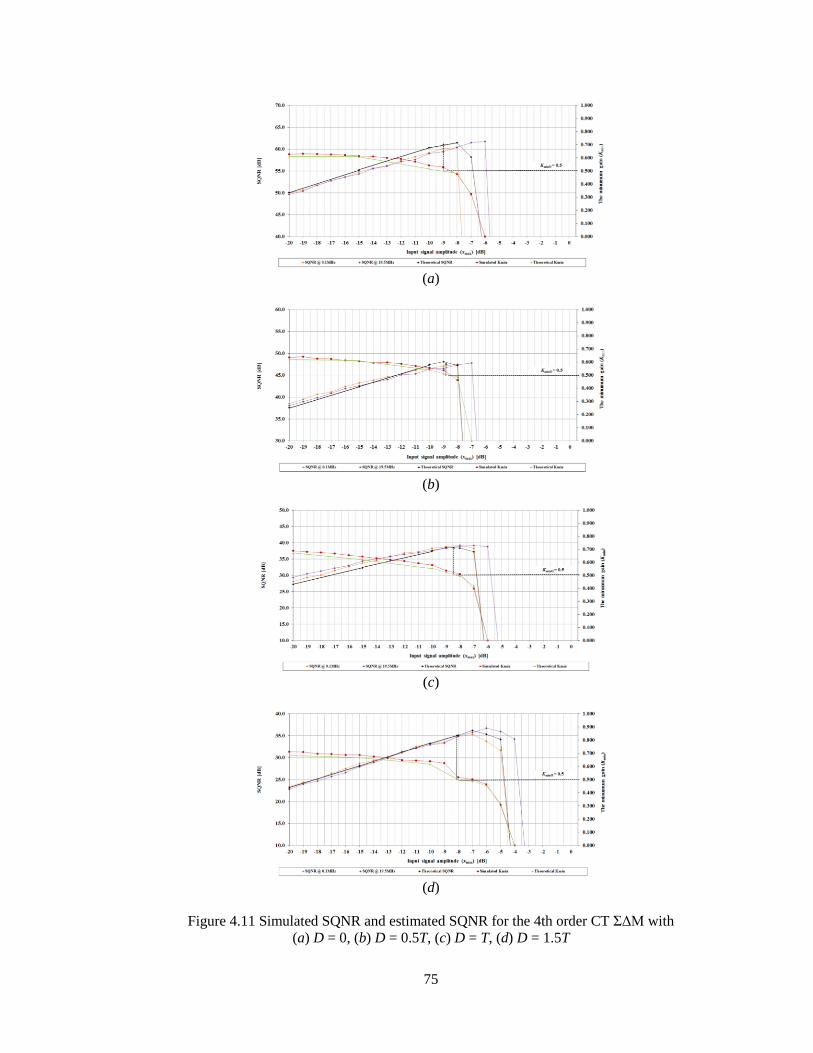
75
(a)
(b)
(c)
(d)
Figure 4.11 Simulated SQNR and estimated SQNR for the 4th order CT ΣΔM with
(a) D = 0, (b) D = 0.5T, (c) D = T, (d) D = 1.5T

76
CHAPTER 5
STABILITY ANALYSIS OF CT ΣΔMS
Because a ΣΔM’s output is typically the output of the ΣΔM’s quantizer, ΣΔMs cannot be
unstable in the bounded input bounded output (BIBO) sense. Instead, a ΣΔM is considered to
have become unstable when the amplitude of a ΣΔM’s input is increased over a value which
causes the ΣΔM’s output SQNR to decrease dramatically and the ΣΔM’s output SQNR cannot
be restored to its previous values even when the ΣΔM’s input is decreased to its previous
amplitudes. In this chapter, a root locus method is used to analyze and predict the maximum
input signal parameters that keep a CT ΣΔM stable.
Root locus methods have been successfully used to determine the stability of DT ΣΔMs;
however, because the denominator terms of both the STF and NTF of a CT ΣΔM contain
exponential functions, traditional root locus methods cannot be used for determining the stability
of CT ΣΔMs. Instead, several other methods have been developed for predicting the stability of
CT ΣΔMs. One such method models the nonlinear quantizer using two linear gains, one for the
signal gain and one for quantization noise gain [35]. This approach has not received much
attention because of its complexity and because it cannot predict stability for several classes of
ΣΔMs. Other approaches predict CT ΣΔM stability by assuming that the ΣΔM has a DC input and
then by performing a simple stability analysis. These methods are effective for predicting stability
for lower order ΣΔMs but not for higher order ΣΔMs [35, 36, 37, 38, 39, 40, 41]. Another method
attempts to determine ΣΔM’s stability by using a one-norm of the ΣΔM’s NTF to determine
stability in a BIBO sense. It has been shown that the one-norm condition is available only for
second order lowpass modulators [43]. Therefore, a mixture of one-norm, two-norm and infinity-
norm constraints have been proposed to predict the stability of higher order modulators [44].
Lee’s rule is another method used to determine the stability of ΣΔMs [45]. Lee’s rule states that a

77
ΣΔM will be stable if the gain of the ΣΔM’s NTF is less than two for all frequencies. It has been
shown that Lee’s rule is neither a necessary nor a sufficient condition to ensure stability in ΣΔMs
[46]. In this chapter, an analytical root locus method is used to determine the stability criteria for
CT ΣΔMs that include exponential functions in their characteristic equations. This root locus
method determines the range of quantizer gains for which a CT ΣΔM is stable. These values can
then be used to determine input signal power and other internal signal powers that prevent the
ΣΔM from becoming unstable.
5.1 Analytical Root Locus
5.1.1 Root locus equation and Gain equation
The poles of a system are the roots of the system’s characteristic equation, and these roots
provide valuable insight concerning the stability and the response of a system. Root locus
analysis is a method for examining how the poles of a system change as function of a certain
system parameter. This method is commonly used to determine the stable region of feedback
systems as a function of open loop gain by plotting the poles of the system’s closed loop transfer
function as a function of the system’s open loop gain.
As shown in (2.20), CT ΣΔMs typically have characteristic equations of the form
1 ( ) ( ) ( ) 0 sDK e G s H s DAC s (5.1)
where D is the ΣΔM’s excess loop delay and DAC(s) is the system function of a DAC which
usually contains at least one exponential function. The root locus analysis of a CT ΣΔM that has a
characteristic equation like the one in (5.1) can be performed using standard graphical analysis
methods [47] or using an analytical method [48, 49] only when D = 0 and DAC(s) = 1. Although
the DAC is not explicitly modeled, a typical zero order hold (ZOH) DAC would have the system
function
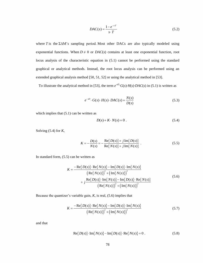
78
1( )
s TeDAC s
s T (5.2)
where T is the ΣΔM’s sampling period. Most other DACs are also typically modeled using
exponential functions. When D ≠ 0 or DAC(s) contains at least one exponential function, root
locus analysis of the characteristic equation in (5.1) cannot be performed using the standard
graphical or analytical methods. Instead, the root locus analysis can be performed using an
extended graphical analysis method [50, 51, 52] or using the analytical method in [53].
To illustrate the analytical method in [53], the term e-sD
∙G(s)∙H(s)∙DAC(s) in (5.1) is written as
( )( ) ( ) ( )
( )
sD N se G s H s DAC s
D s (5.3)
which implies that (5.1) can be written as
( ) ( ) 0 . D s K N s (5.4)
Solving (5.4) for K,
Re ( ) Im ( )( ) .
( ) Re ( ) Im ( )
D s j D sD sK
N s N s j N s
(5.5)
In standard form, (5.5) can be written as
2 2
2 2
Re ( ) Re ( ) Im ( ) Im ( )
Re ( ) Im ( )
Re ( ) Im ( ) Im ( ) Re ( )
Re ( ) Im ( )
D s N s D s N sK
N s N s
D s N s D s N sj
N s N s
(5.6)
Because the quantizer’s variable gain, K, is real, (5.6) implies that
2 2
Re ( ) Re ( ) Im ( ) Im ( )
Re ( ) Im ( )
D s N s D s N sK
N s N s
(5.7)
and that
Re ( ) Im ( ) Im ( ) Re ( ) 0 .D s N s D s N s
(5.8)

79
Plotting (5.8) in the s-plane renders the root locus of (5.1) for -∞ < K < ∞.
5.1.2 Illustrative example of analytical root locus
To illustrate this analytical root locus method, consider a 3rd order CT ΣΔM implemented using
an RC CIFB implementation as shown in Fig 2.9 (a). From Table 2, the STF and NTF of this CT
ΣΔM are
1 0 0
3 2
3 2 2 1 2 0 3 1
2
0 1
3 2
3 2 2 1 1 2 0 3 1 0 0 1 2
1
2
0
1
2
(
(
( ) (1
)
(
)
)
()
)
K b s b c s b c c g b c
s s g c
K M s a s a c
s b c c c
Ss a c c g a c a c c c
s s g c
TF ss
(5.9)
and
3 2
3 2 2 1 1 2 0 3 1 0 0 1 2
2
0 1
.( ) (
1 (
1( )
)
)
K M s a s a c s a c c g a c a c c c
s s
NTFs
g
s
c
(5.10)
Comparing the STF in (2.21) with (5.9) and NTF in (2.22) with (5.10), it can be seen that
3
3 2 2 1 1 2 0 0 1 20 3 1( ) )(F s b s b c s b c c g s b c c cb c (5.11)
2
0 1
1
)( )
(G s
s s g c
(5.12)
3 2
0 0 1 23 2 2 1 1 2 0 3 1( ) ( ) .H s a s a c s a c c g s a c ca c c
(5.13)
Using (5.1), (5.2), (5.12) and (5.13), N(s) and D(s) can be determined to be
3 2
3 2 2 1 1 2 0 3 1 0 0 1 2( ) ( 1) )( sT sDN s a s a c s a c c g a c s a ec c c e
(5.14)
and
2
0 1
2( ) ( ) .s g cD s s T
(5.15)

80
Substituting + j for s where = Re{s} and = Im{s},
4 2 2 2 4 2 2 2
0 1 0 1Re ( ) 3 3 D s T g c g c (5.16)
3 3 3 3
0 1 0 1Im ( ) 3 3 D s T g c g c (5.17)
3 2 2 2
3 3 2 2 2 2 1 1 2 0 3 1 0 0 1 2
( )
2 3
3 3 2 2 1 1 2 0 3 1
Re ( ) 3 (
cos( ) cos(( ) )
3 2 (
sin(
D T D
D
N s a a a c a c a c c g a c a c c c
e D e T D
a a a c a c c g a c
e D ( )) sin(( ) ) T De T D
(5.18)
and
3 2 2 2
3 3 2 2 2 2 1 1 2 0 3 1 0 0 1 2
( )
2 3
3 3 2 2 1 1 2 0 3 1
Im ( ) 3 (
sin( ) sin(( ) )
3 2 (
cos(
D T D
D
N s a a a c a c a c c g a c a c c c
e D e T D
a a a c a c c g a c
e D ( )) cos(( ) ) . T De T D
(5.19)
Substituting (5.16), (5.17), (5.18) and (5.19) into (5.8), the root locus of the 3rd order CT ΣΔM
using an RC implementation can be plotted for -∞ < K < ∞.
Similarly, comparing the STF and the NTF for each order CT ΣΔM shown in Table 2.2 and
Table 2.3 with (2.20) and (2.21), respectively, the F(s), G(s) and H(s) for each order CT ΣΔM can
be determined. Table 5.1 and Table 5.2 show the results. Table 5.1 shows F(s), G(s) and H(s) for
an RC implementation, and Table 5.2 shows F(s), G(s) and H(s) for a GmC implementation. Using
Table 5.1 and Table 5.2, D(s) and N(s) for each order CT ΣΔM can be easily determined to get
the analytical root locus and the quantizer gain value. Table 5.3 and Table 5.4 show Re{D(s)},
Im{D(s)}, Re{N(s)} and Im{N(s)} for RC implementations and GmC implementations,
respectively.
Fig 5.1 (a), (b), (c), (d), (e) and (f) show the root locus or the plot of (5.8), for six lowpass 3rd
order CT ΣΔΜs that have sampling frequencies of 1GHz, Chebyshev Type 2 NTFs with 30dB

81
attenuation in the stopband, and excess loop delays of D = 0, D = 0.5T, D = T, D =1.5T, D =2T,
and D =2.5T, respectively. The plots in Fig 5.1 include both the positive gain (K > 0) root
locus and the negative gain (K < 0) root locus.
(a) (b)
(c) (d)
(e) (f)
Figure 5.1 The root locus of six lowpass 3rd order CT ΣΔΜs that have Chebyshev Type 2 NTFs
with 30dB attenuation in stopband, a sampling frequency of 1GHz, for and excess loop delays of
(a) D = 0, (b) D = 0.5T, (c) D = T, (d) D =1.5T, (e) D =2T, (f) D = 2.5T

82
According to the plots in Fig 5.1, the CT ΣΔΜs with D = 0, D = 0.5T, D = T, and D =1.5T are
stable for 0.240 < K < 8.557, 0.296 < K < 2.893, 0.376 < K < 1.648, and 0.525 < K < 0.986,
respectively. Although the root locus plots show that the CT ΣΔΜs with D = 0, D = 0.5T, D = T,
and D =1.5T are unstable for K > 8.557, K > 2.893, K > 1.648, and K > 0.986, respectively,
none of the modulators show a degradation in SQNR when K enters those ranges because when
the modulator enters unstable regions for large values of quantizer gain, K, the feedback signal
increases which reduces the quantizer gain, K, and moves the poles back into a stable region.
However, when K < 0.240, K < 0.296, K < 0.376, and K < 0.525 for the CT ΣΔΜs with D = 0, D
= 0.5T, D = T, and D =1.5T, respectively, the modulator shows a degradation in SQNR because
when the modulator enters those unstable regions the feedback signal increases which further
reduces the quantizer gain, K, and consequently moves the poles further from the stable region.
Therefore, a CT ΣΔΜ will remain stable if its quantizer gain, K, remains above its minimum
stable value, KminS, as determined from the ΣΔΜ’s root locus plot.
Fig 5.1 (e) and (f) show the root locus plots for the 3rd order CT ΣΔΜs with D = 2T, and D =
2.5T, respectively. These plots show that for both of the cases no quantizer gain, K, exists that can
stabilize the ΣΔΜs. For these cases, a NTF with less attenuation should be chosen. The root loci
in Fig 4.1 also show that the range of the quantizer gains that prevent a ΣΔΜ from becoming
unstable is reduced as the excess loop delay time, D, increases.
Besides root locus plots, Bode plots can also be used to compute the range of quantizer gains
over which a CT ΣΔM is stable. For example, Fig 5.2 shows the Bode plot for the 3rd order CT
ΣΔΜs that has a sampling frequency of 1GHz, uses a Chebyshev Type 2 NTF with 30dB
attenuation in the stopband and has an excess loop delay time, D, of zero. The root locus for this
ΣΔM is shown in Fig 5.1 (a). From Fig 5.2, it can be seen that the lowest stable quantizer gain is -
12.39dB (0.240) and the highest stable quantizer gain is 18.65 dB (8.55). Both of these values are
consistent with the values obtained from the root locus plot in Fig 5.1 (a).

83
Table 5.1 F(s), G(s) and H(s) for RC implementations
2nd order CT ΣΔM
F(s) 2
2 1 1 0 0 1 0 2 0b s b c s b c c g b c
G(s) 2
0 0
1
s g c
H(s) 2
2 1 1 0 0 1 0 2 0( )a s a c s a c c g a c
3rd order CT ΣΔM
F(s) 3 2
3 2 2 1 1 2 0 3 1 0 0 1 2( )b s b c s b c c g b c s b c c c
G(s) 2
0 1
1
( )s s g c
H(s) 3 2
3 2 2 1 1 2 0 3 1 0 0 1 2( )a s a c s a c c g a c s a c c c
4th order CT ΣΔM
F(s) 1 4 2 0 3 0 3
0 0 1 2 3 0 2 0 2
4 3 2
4 3 3 2 2 3 0 4 0 1 1 2 3
3 0 1 4 0 2
( ) ( )
( )
b s b c s b c c g b c s b c c cg b c g b c c s
b c c c c g b c c c g g b c c
G(s) 2 2
0 1 1 2
1
( )( )s g c s g c
H(s)
2
4 1 4 2 1 1 2
4 3
4 3 3 0 3 0 3
0 0 1 2 3 0 2 0 2 3 0 1 4
3 2 2 3 0
0 2
0( )
)
)
(
(
a g a c s a c c c g a c c s
a c c c c g
a s a c s a c c g
a c c c g c
c
g a c
5th order CT ΣΔM
F(s)
2
1 5 3 2 2 3 4 0 4 1 4
1 1 2 3 4 0 3 1 3 4 0 1 5 1 3 0 0 1 2 3
5 4 3
5 4 4 3 3 4 0 5 1
4
)
( )
( ) (g b c g b c c s
b c c c c g b c c c g g b c c
b s b c s b c c g b c s b c c
s b c c
c
c c c
G(s) 2 2
0 1 1 3
1
( () )s s g c s g c
H(s)
3 2
5 1 5 3 2 2 3 4 0 4 1 4
1 1 2 3 4 0 3 1 3 4 0 1 5 1 3 0 0 1 2
5 4
5 4 4 3 3 0 1
4
4
3
( ( )
( )
)a g a c s a c c c g a c c s
a c c c c g a c c c g g a c
a s a c s a
c s a c c c
c c g
c c
c

84
Table 5.2 F(s), G(s) and H(s) for GmC implementations
2nd order CT ΣΔM
F(s) 2
2 1 1 0 0 1 0 2 0 1b s b c s b c g cc b c
G(s) 2
0 0 1
1
s g c c
H(s) 2
2 1 1 0 0 1 0 2 0 1( )a s a c s a c c g a c c
3rd order CT ΣΔM
F(s) 3 2
3 2 2 1 1 2 0 3 1 2 0 0 1 2( )b s b c s b c c g b c c s b c c c
G(s) 2
0 1 2
1
( )s s g c c
H(s) 3 2
3 2 2 1 1 2 0 3 1 2 0 0 1 2( )a s a c s a c c g a c c s a c c c
4th order CT ΣΔM
F(s) 1 1 4 2 3
0 3 0 1 3 0 0 1 2 3 0 2 0
4 3 2
4 3 3 2 2 3
1 2 3
0 4 0
1 1 2 0 1 4 0 1 2 33
(
( )
)
) (
c g b c c
g b c c c s b c c c c g
b s b c s b c c g b c s
b c c b c c c c g g b c c c cc
G(s) 2 2
0 0 1 1 2 3
1
( () )s g c c s g c c
H(s)
2
4 1 4 2 3
1 1 2 3 0 3 0 1 3 0 0 1 2 3 0 2 0 1 2 3 0
4 3
4 3 3 2 2 3 0
1 4 0 2
1
1 3
0( )
( ) ( )
a g a c c s
a c c c g a c c c s a c c c c g a c c c c
a s a c s a c c g
g g c c c c
c
a
c
5th order CT ΣΔM
F(s)
2
2 1 5 3 4 2 2 3 4 0 4 1 2 4
1 1 2 3 4 0 3 1 2 3 4 0 1
5 4 3
5 4 4 3 3 4 0 5 1
5 1 2 3 4 0 0 1 2 3 4
)
(
(
)
(
)b s b c s b c c g b c c g b c c c s
b c c c c g b c c c c g g
c g b c s b c c c
b c c c c s b c c c c c
G(s) 1 1 3 4
2 2
0 2 )( )
1
(s s g c s g cc c
H(s)
3 2
5 2 1 5 3 4 2 2 3 4 0 4 1 2 4
1 1 2 3 4 0 3 1 2 3 4 0 1 5 1 2 3 4 0 0 1
5 4
5 4 4 3 3 4 0 1
2 3 4
)
)
( ( )
(
a c g a c c s a c c c g a c c c s
a c c c c g a c c c c g g a c
a s a c s a
c c c s a c
c c g c
c c c c

85
Table 5.3 Re{D(s)}, Im{D(s)}, Re{N(s)} and Im{N(s)}for RC implementations
2nd order CT ΣΔM
Re{D(s)} 3 2
0 0 3 ) g cT
Im{D(s)} 3 2
0 0( ) g cT
Re{N(s)}
2 2 ( )
2 2 1 1 0 0 1 0 2 0
( )
2 1 1
( ) cos( ) cos(( ) )
2 sin( ) sin(( ) )
D T D
D T D
a a a c a c c g a c e D e T D
a a c e D e T D
Im{N(s)}
2 2 ( )
2 2 1 1 0 0 1 0 2 0
( )
2 1 1
( ) sin( ) sin(( ) )
2 cos( ) cos(( ) )
D T D
D T D
a a a c a c c g a c e D e T D
a a c e D e T D
3rd order CT ΣΔM
Re{D(s)} 4 2 2 2 4 2 2 2
0 1 0 13 3 T g c g c
Im{D(s)} 3 3 3 3
0 1 0 13 3 T g c g c
Re{N(s)}
3 2 2 2
3 3 2 2 2 2 1 1 2 0 3 1 0 0 1 2
( )
2 3
3 3 2 2 1 1 2 0 3 1
( )
3 (
cos( ) cos(( ) )
3 2 (
sin( ) sin(( ) )
D T D
D T D
a a a c a c a c c g a c a c c c
e D e T D
a a a c a c c g a c
e D e T D
Im{N(s)}
3 2 2 2
3 3 2 2 2 2 1 1 2 0 3 1 0 0 1 2
( )
2 3
3 3 2 2 1 1 2 0 3 1
( )
3 (
sin( ) sin(( ) )
3 2 (
cos( ) cos(( ) )
D T D
D T D
a a a c a c a c c g a c a c c c
e D e T D
a a a c a c c g a c
e D e T D
4th order CT ΣΔM
Re{D(s)} 5 3 2 4 3 2
0 1 1 2 0 1 1 210 5 ( ) ( 3 ) T g c g c g g c c
Im{D(s)} 4 2 3 5 2 3
0 1 1 2 0 1 1 25 10 ( ) (3 ) T g c g c g g c c
Re{N(s)}
4 2 2 4 3 2 2 2
4 3 3 2 2 3 0 4 0 1 4 2
1 1 2 3 0 3 0 3 0 0 1 2 3 0 2 0 2 3 0 1 4 0 2
( )
3 3 2 3
4 3 3 2 2 3 0 4
( 6 ) ( 3 ) ( )( )
( ) ( )
cos( ) cos(( ) )
(4 4 ) (3 ) 2(
D T D
a a c a c c g a c g a c
a c c c g a c c a c c c c g a c c c g g a c c
e D e T D
a a c a c c g a
0 1 4 2
1 1 2 3 0 3 0 3
( )
)
( )
sin( ) sin(( ) )
D T D
c g a c
a c c c g a c c
e D e T D

86
Table 5.3 (Continued) Re{D(s)}, Im{D(s)}, Re{N(s)} and Im{N(s)}for RC implementations
Im{N(s)}
4 2 2 4 3 2 2 2
4 3 3 2 2 3 0 4 0 1 4 2
1 1 2 3 0 3 0 3 0 0 1 2 3 0 2 0 2 3 0 1 4 0 2
( )
3 3 2 3
4 3 3 2 2 3 0
( 6 ) ( 3 ) ( )( )
( ) ( )
sin( ) sin(( ) )
(4 4 ) (3 ) 2(
D T D
a a c a c c g a c g a c
a c c c g a c c a c c c c g a c c c g g a c c
e D e T D
a a c a c c g a
4 0 1 4 2
1 1 2 3 0 3 0 3
( )
)
( )
cos( ) cos(( ) )
D T D
c g a c
a c c c g a c c
e D e T D
5th order CT ΣΔM
Re{D(s)}
6 4 2 2 4 6 4 2 2 4
0 1 1 3
2 2
0 1 1 3
15 15 ( ) ( 6 )
)
g c g cT
g g c c
Im{D(s)} 5 3 3 5 3 3
0 1 1 3 0 1 1 320 6 ( ) (4 4 ) 2 T g c g c g g c c
Re{N(s)}
5 3 2 4 4 2 2 4
5 4 4
3 2
3 3 4 0 5 1 1 5 3
2 2
2 2 3 4 0 4 1 4 1 1 2 3 4 0 3 1 3 4 0 1 5 1 3
0 0 1 2 3 4
( )
( 10 5 ) ( 6 )
( )( 3 )
( )( ) ( )
cos( ) cos(( ) )
D T D
a a c
a c c g a c g a c
a c c c g a c c a c c c c g a c c c g g a c c
a c c c c c
e D e T D
4 2 3 5 3 3
5 4 4
2 3
3 3 4 0 5 1 1 5 3
2 2 3 4 0 4 1 4 1 1 2 3 4 0 3 1 3 4 0 1 5 1 3
( )
(5 10 ) (4 )
( )(3 )
2( ) ( )
sin( ) sin(( ) )
D T D
a a c
a c c g a c g a c
a c c c g a c c a c c c c g a c c c g g a c c
e D e T D
Im{N(s)}
5 3 2 4 4 2 2 4
5 4 4
3 2
3 3 4 0 5 1 1 5 3
2 2
2 2 3 4 0 4 1 4 1 1 2 3 4 0 3 1 3 4 0 1 5 1 3
0 0 1 2 3 4
( )
( 10 5 ) ( 6 )
( )( 3 )
( )( ) ( )
sin( ) sin(( ) )
D T D
a a c
a c c g a c g a c
a c c c g a c c a c c c c g a c c c g g a c c
a c c c c c
e D e T D
4 2 3 5 3 3
5 4 4
2 3
3 3 4 0 5 1 1 5 3
2 2 3 4 0 4 1 4 1 1 2 3 4 0 3 1 3 4 0 1 5 1 3
( )
(5 10 ) (4 )
( )(3 )
2( ) ( )
cos( ) cos(( ) )
D T D
a a c
a c c g a c g a c
a c c c g a c c a c c c c g a c c c g g a c c
e D e T D
87
Table 5.4 Re{D(s)}, Im{D(s)}, Re{N(s)} and Im{N(s)}for GmC implementations
2nd order CT ΣΔM
Re{D(s)} 3 2
0 0 13 g cT c
Im{D(s)} 2 3
0 0 1( ) T g c c
Re{N(s)}
2 2 ( )
2 2 1 1 0 0 1 0 2 0 1
( )
2 1 1
( ) cos( ) cos(( ) )
2 sin( ) sin(( ) )
D T D
D T D
a a a c a c c g a c c e D e T D
a a c e D e T D
Im{N(s)}
2 2 ( )
2 2 1 1 0 0 1 0 2 0 1
( )
2 1 1
( ) sin( ) sin(( ) )
2 cos( ) cos(( ) )
D T D
D T D
a a a c a c c g a c c e D e T D
a a c e D e T D
3rd order CT ΣΔM
Re{D(s)} 4 2 2 2 4 2 2 2
0 1 2 0 1 23 3 T g c c g c c
Im{D(s)} 3 3 3 3
0 1 2 0 1 23 3 T g c c g c c
Re{N(s)}
3 2 2 2
3 3 2 2 2 2 1 1 2 0 3 1 2 0 0 1 2
( )
2 3
3 3 2 2 1 1 2 0 3 1 2
( )
3 (
cos( ) cos(( ) )
3 2 (
sin( ) sin(( ) )
D T D
D T D
a a a c a c a c c g a c c a c c c
e D e T D
a a a c a c c g a c c
e D e T D
Im{N(s)}
3 2 2 2
3 3 2 2 2 2 1 1 2 0 3 1 2 0 0 1 2
( )
2 3
3 3 2 2 1 1 2 0 3 1 2
( )
3 (
sin( ) sin(( ) )
3 2 (
cos( ) cos(( ) )
D T D
D T D
a a a c a c a c c g a c c a c c c
e D e T D
a a a c a c c g a c c
e D e T D
4th order CT ΣΔM
Re{D(s)} 5 3 2 4 3 2
0 0 1 1 2 3 0 1 0 1 2 310 5 ( ) ( 3 ) T g c c g c c g g c c c c
Im{D(s)} 4 2 3 5 2 3
0 0 1 1 2 3 0 1 0 1 2 35 10 ( ) (3 ) T g c c g c c g g c c c c
Re{N(s)}
4 2 2 4 3 2 2 2
4 3 3 2 2 3 0 4 0 1 1 4 2 3
1 1 2 3 0 3 0 1 3 0 0 1 2 3 0 2 0 1 2 3 0 1 4 0 1 2 3
( )
3 3 2 3
4 3 3
( 6 ) ( 3 ) ( )( )
( ) ( )
cos( ) cos(( ) )
(4 4 ) (3 ) 2
D T D
a a c a c c g a c c g a c c
a c c c g a c c c a c c c c g a c c c c g g a c c c c
e D e T D
a a c
2 2 3 0 4 0 1 1 4 2 3
1 1 2 3 0 3 0 1 3
( )
( )
( )
sin( ) sin(( ) )
D T D
a c c g a c c g a c c
a c c c g a c c c
e D e T D

88
Table 5.4 (Continued) Re{D(s)}, Im{D(s)}, Re{N(s)} and Im{N(s)}for GmC implementations
Im{N(s)}
4 2 2 4 3 2 2 2
4 3 3 2 2 3 0 4 0 1 1 4 2 3
1 1 2 3 0 3 0 1 3 0 0 1 2 3 0 2 0 1 2 3 0 1 4 0 1 2 3
( )
3 3 2 3
4 3 3
( 6 ) ( 3 ) ( )( )
( ) ( )
sin( ) sin(( ) )
(4 4 ) (3 )
D T D
a a c a c c g a c c g a c c
a c c c g a c c c a c c c c g a c c c c g g a c c c c
e D e T D
a a c
2 2 3 0 4 0 1 1 4 2 3
1 1 2 3 0 3 0 1 3
( )
2( )
( )
cos( ) cos(( ) )
D T D
a c c g a c c g a c c
a c c c g a c c c
e D e T D
5th order CT ΣΔM
Re{D(s)}
6 4 2 2 4 6 4 2 2 4
0 1 2 1 3 4
2 2
0 1 1 2 3 4
15 15 ( ) ( 6 )
)
g c c g c cT
g g c c c c
Im{D(s)} 5 3 3 5 3 3
0 1 2 1 3 4 0 1 1 2 3 420 6 ( ) (4 4 ) 2 T g c c g c c g g c c c c
Re{N(s)}
5 3 2 4 4 2 2 4
5 4 4
3 2
3 3 4 0 5 1 2 1 5 3 4
2 2
2 2 3 4 0 4 1 2 4 1 1 2 3 4 0 3 1 2 3 4 0 1 5 1 2 3 4
0 0 1 2 3 4
( )
( 10 5 ) ( 6 )
( )( 3 )
( )( ) ( )
cos( )
D T D
a a c
a c c g a c c g a c c
a c c c g a c c c a c c c c g a c c c c g g a c c c c
a c c c c c
e D e
4 2 3 5 3 3
5 4 4
2 3
3 3 4 0 5 1 2 1 5 3 4
2 2 3 4 0 4 1 2 4 1 1 2 3 4 0 3 1 2 3 4 0 1 5 1 2 3 4
( )
cos(( ) )
(5 10 ) (4 )
( )(3 )
2( ) ( )
sin( ) sin(( ) )
D T D
T D
a a c
a c c g a c c g a c c
a c c c g a c c c a c c c c g a c c c c g g a c c c c
e D e T D
Im{N(s)}
5 3 2 4 4 2 2 4
5 4 4
3 2
3 3 4 0 5 1 2 1 5 3 4
2 2
2 2 3 4 0 4 1 2 4 1 1 2 3 4 0 3 1 2 3 4 0 1 5 1 2 3 4
0 0 1 2 3 4
( )
( 10 5 ) ( 6 )
( )( 3 )
( )( ) ( )
sin( )
D T D
a a c
a c c g a c c g a c c
a c c c g a c c c a c c c c g a c c c c g g a c c c c
a c c c c c
e D e
4 2 3 5 3 3
5 4 4
2 3
3 3 4 0 5 1 2 1 5 3 4
2 2 3 4 0 4 1 2 4 1 1 2 3 4 0 3 1 2 3 4 0 1 5 1 2 3 4
( )
sin(( ) )
(5 10 ) (4 )
( )(3 )
2( ) ( )
cos( ) cos(( ) )
D T D
T D
a a c
a c c g a c c g a c c
a c c c g a c c c a c c c c g a c c c c g g a c c c c
e D e T D

89
Figure 5.2 Bode plot for the 3rd order CT ΣΔΜ shown in Fig 5.1 (a)
5.2 Stability Analysis for CT ΣΔΜs that are not overloaded
Because the output of a ΣΔΜ’s quantizer has fixed quantization levels, its gain is a function of
its input signal which is a function of the ΣΔΜ’s input signal. Therefore, the stability of a CT
ΣΔΜ depends upon the quantizer’s input signal because a large enough input signal can generate
a large signal at the quantizer’s input which reduces the quantizer’s gain and in turn can
destabilize the modulator loop. In this section, a method for determining a ΣΔΜ’s maximum
input signal power which keeps the ΣΔΜ stable is developed.
To determine the maximum input signal power, maxS,P that keeps a ΣΔM stable, consider the
STF and NTF models shown in Fig 5.3 (a) and (b) and assume that the quantizer’s input, , is a
zero mean random process. Because is a zero mean random process, the quantizer’s input
signal power, ,P can be written as 2P where is the standard deviation of . To keep a
ΣΔM stable, maxS < 1/KminS where
maxS is the quantizer’s maximum input amplitude that keeps
the ΣΔM stable. This condition is assumed to be true when maxS or equivalently when
0.0
0.1
0.2
0.3
0.4
0.5
0.6
0.7
0.8
0.9
1.0
0.0
5.0
10.0
15.0
20.0
25.0
30.0
35.0
40.0
45.0
50.0
-20 -19 -18 -17 -16 -15 -14 -13 -12 -11 -10 -9 -8 -7 -6 -5 -4 -3 -2 -1 0T
he
min
imu
m g
ain
(K
min
)
SQ
NR
[
dB
]
Input Signal Amplitude(xmax) [dB]
SQNR
Kmin
Kmin_no overload = 0.5

90
22
2 maxS
minS
1
K
(5.20)
where
is the standard deviation coefficient of as shown in Fig 5.4. Based on the empirical
simulation results, is chosen as 3.6. Because the minimum quantizer gain that keeps a ΣΔM
stable is KminS, the quantizer’s maximum input power, maxS
,P that keeps a ΣΔM stable can be
written as
maxS maxS
2
2
minS
1.P
K
(5.21)
(a)
(b)
Figure 5.3 (a) Block diagram of a CT ΣΔM’s STF, (b) Block diagram of a CT ΣΔM’s NTF
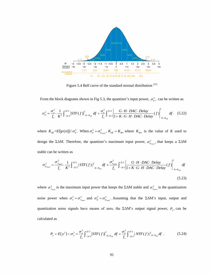
91
Figure 5.4 Bell curve of the standard normal distribution [22]
From the block diagrams shown in Fig 5.3, the quantizer’s input power, 2 , can be written as
22 2/2 /222
2 /2 /2
1( ) ( ) .
1eff
eff
fs fsx e
K Kfs fss s K K
G H DAC DelaySTF f df f df
f K f K G H DAC Delay
(5.22)
where 2= [ ( ) ] / .effK E n WhenmaxS
2 2 , eff desK K where desK is the value of K used to
design the ΣΔM. Therefore, the quantizer’s maximum input power, maxS
2 , that keeps a ΣΔM
stable can be written as
maxS maxS
maxS
22 2/2 /2
2 2
2 /2 /2
1| ( ) | ( )
1desdes
fs fsx e
fs fsK Ks s K K
G H DAC DelaySTF f df f df
f K f K G H DAC Delay
(5.23)
where maxS
2
x is the maximum input power that keeps the ΣΔM stable and maxS
2
e is the quantization
noise power when maxS
2 2
x x and maxS
2 2 . Assuming that the ΣΔM’s input, output and
quantization noise signals have means of zero, the ΣΔΜ’s output signal power, ,yP can be
calculated as
2 2/2 /22 2
/2 /2
2 2 ( ) | ( ) |[ .]effeff
fs fsx e
K KK Kfs fss s
y y STF f df NTF f dff
P E yf
(5.24)

92
Therefore, at the maximum values of 2
x and 2
e that keep the ΣΔM stable,
maxS maxS
2 2/2 /2
22 2
/2 /2| ( ) | | ( ) | .
des des
fs fsx e
K K K Kfs s
s
yf
s
STF f df NTF f dff f
(5.25)
Subtracting (5.22) from (5.24) and solving the resulting equation for 2 ,e the quantization noise
power, 2 ,e can be determined as
2 2
2
2/2 /2
2
/2 /2
.
1| ( ) | ( )
1
eff
eff
y
e
fs fs
K Kfs fs
s K K
G H DAC DelayNTF f df f df
f K G H DAC Delay
(5.26)
Therefore, the maximum quantization noise power, maxS
2 ,e that keeps a ΣΔM stable can be
determined as
maxS
maxS
2 2
2
2/2 /2
2
/2 /2
1| ( ) | ( )
1des
des
y
e
fs fs
K Kfs fs
s K K
G H DAC DelayNTF f df f df
f K G H DAC Delay
(5.27)
Using (5.25), the maximum input power, maxS
,xP that keeps a ΣΔM stable can be determined as
maxS
maxS maxS
2/2
2 2
/22
/22
/2
| ( ) |
1
|
( |
)
des
des
fse
yfs K K
sx x fs
K Kfs
s
NTF f dff
P
STF f dff
(5.28)
where 2 y is 1 for a single-bit quantizer and
maxS
2
e is given in (5.27).
5.3 Stability Analysis Example of ΣΔΜs that are not overloaded
To illustrate this method, consider two 4th order ΣΔΜs where one of the ΣΔΜs has a sampling
frequency of 1GHz, a Chebyshev Type 2 NTF with 21dB of attenuation, an excess loop delay of
2T and the root loci shown in Fig 5.5 (a) and the other ΣΔΜ has a sampling frequency of 1GHz, a
Chebyshev Type 2 NTF with 18dB of attenuation, an excess loop delay of 2.5T and the root loci

93
shown in Fig 5.5 (b).
(a) (b)
Figure 5.5 The root locus of 4th order CT ΣΔΜs that uses Chebyshev Type 2 NTFs
with a sampling frequency of 1GHz for (a) D = 2T, (b) D = 2.5T
From inspection of the plots, the 4th order CT ΣΔΜs with D = 2T and D = 2.5T are stable when
the minimum quantizer gains, KminS, are 0.508 and 0.530, respectively. Because these KminSs are
greater than KminO (0.5), the CT ΣΔM will not be overloaded before becoming unstable. Assuming
a single bit quantizer with an output of ±1, the maximum quantizer inputs, ψmaxS, that prevent the
CT ΣΔΜs from becoming unstable can be calculated as
maxS
minS
1 11.968
0.508K (5.29)
and
maxS
minS
1 11.886.
0.530K (5.30)
Therefore, the CT ΣΔΜs with D = 2T and D = 2.5T are unstable when ψmaxS > 1.968 and ψmaxS >
1.886, respectively. Using (5.21), quantizers’ maximum input powers, maxS
2 , are
maxS
2 2
2
minS
1 1= 0.299 for = 2
3.6 0.508D T
K
(5.31)

94
and
maxS
2 2
2
minS
1 1= 0.275 for = 2.5 .
3.6 0.530D T
K
(5.32)
Using (5.27), (5.31) and (5.32), the quantization noise powers, maxS
2 ,e that keeps the ΣΔMs stable
can be determined as
maxS
2 0.271 for = 23.331 0.7
1 0.2
4
99
4e D T
(5.33)
and
maxS
2 0.276 for = 2.53.416 0.78
1 0.275
9e D T
(5.34)
where the term /2
2
/2
1| ( ) |
des
fs
K Kfs
s
NTF f dff
and
the term
2/2
/2
1( )
1des
fs
fss K K
G H DAC Delayf df
f K G H DAC Delay
were calculated using the following
Matlab code and Kdes was set to one in this example.
% The coefficients of transfer function F(s),G(s)and H(s)
% F(s)= F4*s^4+F3*s^3+F2*s^2+F1*s+F0;
% G(s)= 1/(s^4+G2*s^2+G0);
% H(s)= H3*s^3+H2*s^2+H1*s+H0;
%fs: Sampling frequency
%T=1/fs: Sampling period
%D:Excess loop delay
NTFsq=@(f)abs(((j.*2*pi.*f).^4+G2.*(j.*2*pi.*f).^2+G0).*((j.*2*pi.*f).*T)./
((j.*2*pi.*f).*T.*((j.*2*pi.*f).^4+G2.*(j.*2*pi.*f).^2+G0)+K.*(H3.*(j.*2*pi.*f)
.^3+H2.*(j.*2*pi.*f).^2+H1.*(j.*2*pi.*f)+H0).*(1-exp(-(j.*2*pi.*f).*T)).*exp(-
(j.*2*pi.*f).*D))).^2;
NTF=integral(NTFsq,-fs/2,fs/2)/fs;
GHDACsq=@(f)abs(((H3.*(j.*2*pi.*f).^3+H2.*(j.*2*pi.*f).^2+H1.*(j.*2*pi.*f)+H0).
*(1-exp(-(j.*2*pi.*f).*T)).*exp(-(j.*2*pi.*f).*D))./
((j.*2*pi.*f).*T.*((j.*2*pi.*f).^4+G2.*(j.*2*pi.*f).^2+G0)+(K.*(H3.*(j.*2*pi.*f
).^3+H2.*(j.*2*pi.*f).^2+H1.*(j.*2*pi.*f)+H0).*(1-exp(-(j.*2*pi.*f).*T))
.*exp(-(j.*2*pi.*f).*D)))).^2;
GHDAC=integral(GHDACsq,-fs/2,fs/2)/fs;

95
Using (5.28), (5.33), and (5.34), the maximum input powers, maxS
,xP that keep the ΣΔMs stable are
maxS maxS
2 0.271 3.331 = 0.097 for = 21 x xP D T (5.35)
and
maxS maxS
2 0.276 3.416 = 0.057 for1 = 2.5x xP D T (5.36)
where the term /2
2
/2
1| ( ) |
des
fs
fs K Ks
STF f dff was calculated using the following Matlab code.
% F(s) =F4*s^4+F3*s^3+F2*s^2+F1*s+F0;
% G(s)= 1/(s^4+G2*s^2+G0);
% H(s)= H3*s^3+H2*s^2+H1*s+H0;
STFsq=@(f)abs(((F4.*(j.*2*pi.*f).^4+F3.*(j.*2*pi.*f).^3+F2.*(j.*2*pi.*f).^2+F1.
*(j.*2*pi.*f)+F0.*(j.*2*pi.*f).*T)
./(((j.*2*pi.*f).^4+G2.^(j.*2*pi.*f).^2+G0).*(j.*2*pi.*f).*T+(H3.*(j.*2*pi.*f).
^3+H2.*(j.*2*pi.*f).^2+H1.*(j.*2*pi.*f)+H0).*(1-exp(-(j.*2*pi.*f).*T)).*exp(-
(j.*2*pi.*f).*D))).^2;
STF=integral(STFsq,-fs/2,fs/2)/fs;
Assuming a sinusoidal input signal, the maxmum input signal power, maxS
,xP can be written as
maxS maxS
2 2
maxS / 2x xP x (5.37)
where xmaxS is the ΣΔΜ’s maximum input amplitude that keeps a ΣΔM stable. Using (5.35),
(5.36), and (5.37), xmaxS is estimated to be 0.441 (-7.1dB) for the 4th order CT ΣΔΜs with D = 2T
and 0.339 (-9.4dB) for the 4th order CT ΣΔΜs with D = 2.5T.
Fig 5.6 (a) shows the simulated SQNR and minimum quantizer gain for the 4th order CT ΣΔΜ
with D = 2T in this example. The simulation results show that when K=KminS0.510, the
sinusoidal input signal has an amplitude of -7.4dB. The simulation results also show that the
actual maximum sinusoidal input amplitude for the stability is -7.0dB which is close to the
predicted maximum amplitude of -6.9dB.
Fig 5.6 (b) shows the simulated SQNR and minimum quantizer gain for the 4th order CT ΣΔΜ
with D = 2.5T in this example. The simulation results show that when K=KminS0.534, the

96
sinusoidal input signal has an amplitude of -9.8dB. The simulation results also show that the
actual maximum sinusoidal input amplitude for the stability is -8.0dB which is close to the
predicted maximum amplitude of -9.1dB.
(a)
(b)
Figure 5.6 Simulated SQNR and the minimum quantizer gain (Kmin) using a sinusoidal input
for the 4th order CT with (a) D = 2T, (b) D =2.5T

97
5.4 Other Stability Simulation Results of CT ΣΔMs that are not overloaded
To illustrate this methodology’s accuracy for predicting xmaxS, five 5th order CT s were
also simulated. Table 5.5 shows the specification for the five 5th order as well as the two 4th
order s discussed in Secion 5.3. For each of the CT s, the predicted xmaxS is compared to
the simulated xmaxS.
Table 5.6 compares the theoretical minimum quantizer gain, KminS, obtained from the analytical
root locus with the simulated minimum quantizer gain obtained when the simulated input signal is
a sinusoidal that has an amplitude of xmaxS, the maximum predicted amplitude that keeps the
stable. Table 5.7 compares the predicted maximum input amplitude with the simulated
maximum input amplitude that keeps the stable. This table shows that all but one of the
predictions are within 1dB of the simulation results.
Table 5.5 Specification for each CT
(a) Common specification
(b) NTF attenuation for each CT
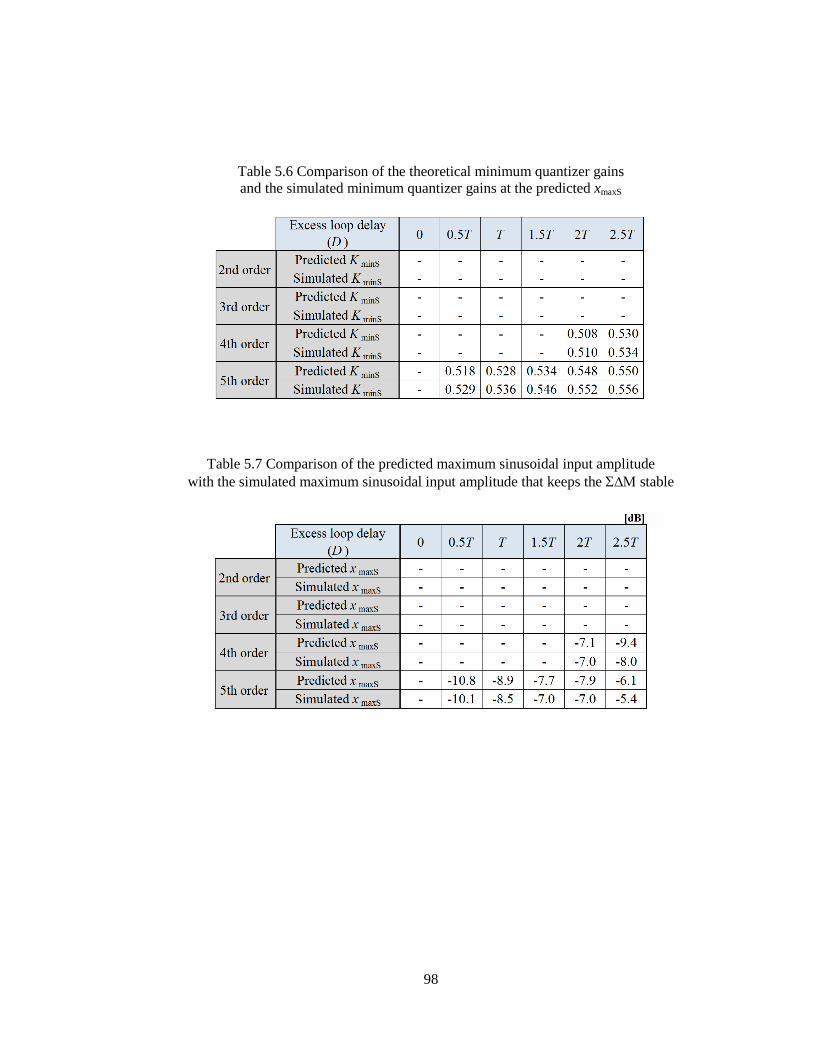
98
Table 5.6 Comparison of the theoretical minimum quantizer gains
and the simulated minimum quantizer gains at the predicted xmaxS
Table 5.7 Comparison of the predicted maximum sinusoidal input amplitude
with the simulated maximum sinusoidal input amplitude that keeps the stable
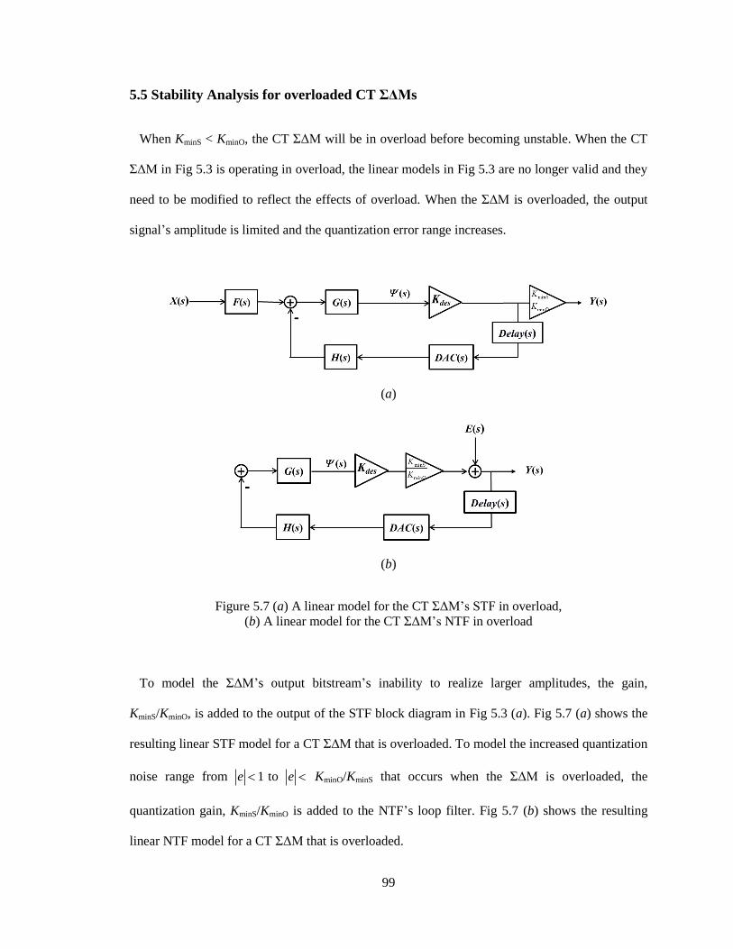
99
5.5 Stability Analysis for overloaded CT ΣΔΜs
When KminS < KminO, the CT ΣΔM will be in overload before becoming unstable. When the CT
ΣΔM in Fig 5.3 is operating in overload, the linear models in Fig 5.3 are no longer valid and they
need to be modified to reflect the effects of overload. When the ΣΔM is overloaded, the output
signal’s amplitude is limited and the quantization error range increases.
(a)
(b)
Figure 5.7 (a) A linear model for the CT ΣΔM’s STF in overload,
(b) A linear model for the CT ΣΔM’s NTF in overload
To model the ΣΔM’s output bitstream’s inability to realize larger amplitudes, the gain,
KminS/KminO, is added to the output of the STF block diagram in Fig 5.3 (a). Fig 5.7 (a) shows the
resulting linear STF model for a CT ΣΔM that is overloaded. To model the increased quantization
noise range from 1e to e KminO/KminS that occurs when the ΣΔM is overloaded, the
quantization gain, KminS/KminO is added to the NTF’s loop filter. Fig 5.7 (b) shows the resulting
linear NTF model for a CT ΣΔM that is overloaded.
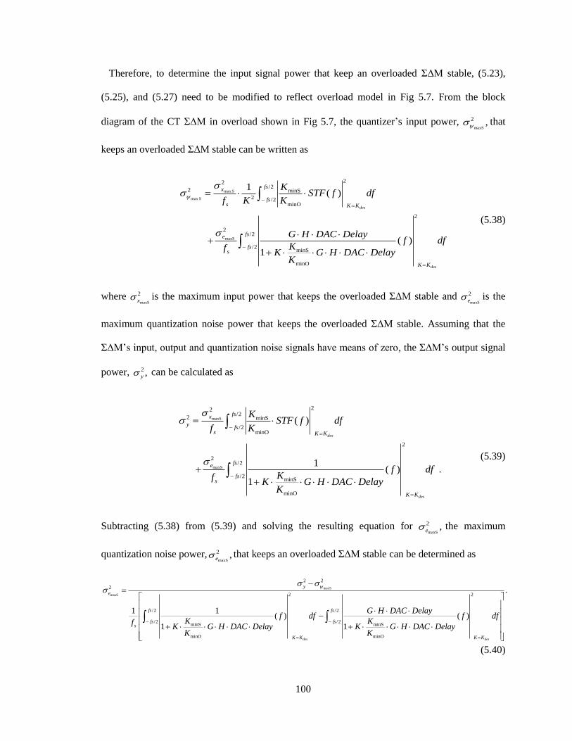
100
Therefore, to determine the input signal power that keep an overloaded ΣΔM stable, (5.23),
(5.25), and (5.27) need to be modified to reflect overload model in Fig 5.7. From the block
diagram of the CT ΣΔM in overload shown in Fig 5.7, the quantizer’s input power, maxS
2 , that
keeps an overloaded ΣΔM stable can be written as
max S
max S
maxS
22/2
2 minS
2 /2minO
2
2/2
/2minS
minO
1( )
( )
1
des
des
fsx
fss K K
fse
fss
K K
KSTF f df
f K K
G H DAC Delayf df
KfK G H DAC Delay
K
(5.38)
where maxS
2 xis the maximum input power that keeps the overloaded ΣΔM stable and
maxS
2 eis the
maximum quantization noise power that keeps the overloaded ΣΔM stable. Assuming that the
ΣΔΜ’s input, output and quantization noise signals have means of zero, the ΣΔM’s output signal
power, 2 , y can be calculated as
maxS
maxS
22/2
minS
/2minO
2
2/2
/2minS
minO
2 ( )
1( ) .
1
des
des
fsx
fss K K
fs
s
y
e
fs
K K
KSTF f df
f K
f dfKf
K G H DAC DelayK
(5.39)
Subtracting (5.38) from (5.39) and solving the resulting equation for maxS
2 , ethe maximum
quantization noise power,maxS
2 , ethat keeps an overloaded ΣΔM stable can be determined as
maxS
maxS
2 2
2
2 2
/2 /2
/2 /2minS minS
minO minO
.
1 1( ) ( )
1 1
des des
y
e
fs fs
fs fss
K K K K
G H DAC Delayf df f df
K KfK G H DAC Delay K G H DAC Delay
K K
(5.40)

101
Using (5.39), the maximum input power, maxS
,xP that keeps an overloaded ΣΔM stable can be
determined as
maxS
maxS maxS
2
2/2
2
/2minS
minO2
2/2
minS
/2minO
1( )
1
1
( )
des
des
fse
yfs
s
K K
x xfs
fss K K
f dfKf
K G H DAC DelayK
PK
STF f dff K
(5.41)
where 2 y is 1 for a single-bit quantizer and
maxS
2 e is given in (5.40).
5.6 Stability Analysis Example of an overloaded ΣΔΜ
To illustrate this method, consider the root loci in Fig 5.8 (a), (b) and (c) which show the root
loci for 3rd order ΣΔΜs with sampling frequencies of 1GHz, Chebyshev Type 2 NTFs with 47dB,
37dB, and 30dB attenuation in the stopband, respectively, and excess loop delay times, D, of 0,
0.5T, and T, respectively. From inspection of the plots, the CT ΣΔΜs with D = 0, D = 0.5T, and D
= T are stable when the minimum quantizer gains, KminS, are 0.326, 0.359, and 0.376, respectively.
Assuming a single bit quantizer with an output of ±1, the maximum quantizer input, ψmaxS, that
prevents the CT ΣΔΜs from becoming unstable is
maxS
minS
1.
K (5.42)
Therefore, the CT ΣΔΜs with D = 0, D = 0.5T, and D = T are unstable when ψmaxS > 3.07, ψmaxS >
2.78, and ψmaxS > 2.66, respectively.
Consider the 3rd order CT ΣΔΜ that has an excess loop delay of D = T of the root locus shown
in Fig 5.8 (c). Because KminS< KminO, this ΣΔΜ will be overloaded when it becomes unstable. To
predict the maximum input signal power that keeps the ΣΔΜ stable, (5.21) can be used to
determine

102
maxS
2 2
2
minS
1 1= 0.546
3.6 0.376K
(5.43)
where KminS = 0.376 and = 3.6.
(a) (b)
(c)
Figure 5.8 The root locus of 3rd order CT ΣΔΜs that uses Chebyshev Type 2 NTFs
with a sampling frequency of 1GHz for (a) D = 0, (b) D = 0.5T, (c) D = T
Using (5.40) and (5.43), the quantization noise power, maxS
2 ,e that keeps this ΣΔM stable when
overloaded can be determined as
maxS
2 0.5460.290
3.329 1.7
1
63e
(5.44)

103
where the term
2
/2
/2minS
minO
1 1( )
1
des
fs
fss
K K
f dfKf
K G H DAC DelayK
and the term
2
/2
/2minS
minO
1( )
1
des
fs
fss
K K
G H DAC Delayf df
KfK G H DAC Delay
K
were calculated using the following Matlab
code and Kdes was set to one in this example.
% The coefficients of transfer function F(s),G(s)and H(s)
% F(s)= F3*s^3+F2*s^2+F1*s+F0
% G(s)= 1/(s^3+G1*s)
% H(s)= H3*s^3+H2*s^2+H1*s+H0
%fs: Sampling frequency
%T=1/fs Sampling period
%D:Excess loop delay
%kminS:The maximum quantizer gain that keeps a ΣΔM stable
%kminO:The maximum quantizer gain that prevents a ΣΔM from overloading
NTFsq=@(f)abs((((j.*2*pi.*f).^3+G1.*j.*2*pi.*f).*(j.*2*pi.*f.*T))...
./(((j.*2*pi.*f).^3+a.*j.*2*pi.*f).*(j.*2*pi.*f.*T)+K.*(kminS/kminO).*
(H2.*(j*2*pi.*f).^2+H1.*(j.*2*pi.*f)+H0).*(1-exp(-j.*2*pi.*f.*T)).*exp(-
j.*2*pi.*f.*D))).^2;
NTF=integral(NTFsq,-fs/2,fs/2)/fs;
GHDACsq=@(f)(abs((H2.*(j.*2*pi.*f).^2+H1.*(j.*2*pi.*f)+H0).*(1-exp(-
j.*2*pi.*f*T)).*exp(-j.*2*pi.*f*D)./(((j.*2*pi.*f).^3+G1.*j.*2*pi.*f).
*(j.*2*pi.*f.*T)+K.*(kminS/kminO).*(H2.*(j.*2*pi.*f).^2+H1.*(j.*2*pi.*f)+H0).*(
1-exp(-j.*2*pi.*f*T)).*exp(-j.*2*pi.*f.*D)))).^2;
GHDAC=integral(GHDACsq,-fs/2,fs/2)/fs;
Using (5.41) and (5.44), the maximum input power, maxS
,xP that keeps this ΣΔM stable when
overloaded is
maxS maxS
2
2
0.290 3.329 = 0.061 .
0.376
0.5
1 x xP
(5.45)
where the term
2/2
minS
/2minO
1( )
des
fs
fss K K
KSTF f df
f K
was calculated using the following Matlab code.

104
% F(s) = F3*s^3+F2*s^2+F1*s+F0
% G(s):1/(s^3+G1*s)
% H(s)= H3*s^3+H2*s^2+H1*s+H0
STFsq=@(f)abs.*((kminS/kminO).*((F3.*(j.*2*pi.*f).^3+F2.*(j.*2*pi.*f).^2+F1.*(j
.*2*pi.*f)+F0)).*(j.*2*pi.*f).*T)...
./(((j.*2*pi.*f).^3+a.*j.*2*pi.*f).*(j.*2*pi.*f.*T)+(H2.*(j.*2*pi.*f).^2+H1.*(j
.*2*pi.*f)+H0).*(1-exp(-j.*2*pi.*f.*T)).*exp(-j.*2*pi.*f.*D))).^2;
STF=integral(STFsq,-fs/2,fs/2)/fs;
Assuming a sinusoidal input signal,
maxS maxS
2 2
maxS / 2x xP x (5.46)
where xmaxS is the ΣΔΜ’s maximum input amplitude that keep the ΣΔΜ stable in overload. Using
(5.45) and (5.46), xmaxS is estimated to be 0.349 (-9.1dB).
Fig 5.9 shows the simulated SQNR and minimum quantizer gain for the 3rd order CT ΣΔΜ
with D = T in this example. The simulation results show that the sinusoidal input amplitude is
-8.5dB when Kmin is 0.387. The results also show that the ΣΔΜ becomes unstable when the
maximum sinusoidal input is greater than -7.0dB and Kmin is 0.306.
Figure 5.9 Simulated SQNR and the minimum quantizer gain (Kmin) using a sinusoidal input
for the 3rd order CT with D = T in example

105
The maximum sinusoidal input amplitudes, xmaxS were also predicted for the other 3rd order CT
ΣΔΜs that have the root loci shown in Fig 5.8 (a) and (b). Their xmaxS values were predicted to be
0.457 (-6.8dB) and 0.484 (-6.3dB) for the CT ΣΔΜs that have the root loci shown in Fig. 5.8 (a)
and (b), respectively. These ΣΔΜs were also simulated using a sinusoidal input with a frequency
of 0.1MHz.
(a)
(b)
Figure 5.10 Simulated SQNR and the quantizer’s minimum gain (Kmin)
for the 3rd order CT for (a) D = 0 (b) D = 0.5T

106
Fig 5.10 (a) shows the SQNRs and the quantizer’s minimum gain, Kmin, as a function of input
signal’s amplitude for the ΣΔΜ with D = 0. As shown in the Fig 5.10 (a), the ΣΔΜ’s SQNR
increases linearly until the input signal’s amplitude is approximately -12 dB, and Kmin = 0.508. As
the input signal’s amplitude is increased above -12 dB, the SQNR increases nonlinearly as a
function of input signal’s amplitude because the ΣΔΜ is overloaded. As the input signal’s
amplitude is increased above -6 dB, the ΣΔΜ’s SQNR degrades dramatically and the ΣΔΜ’s
SQNR cannot be restored to its previous values even when the ΣΔM’s input is decreased to its
previous amplitudes. As mentioned earlier, the maximum sinusoidal input amplitude was
predicted to be -6.8dB when KminS is 0.326. The simulation results show that the sinusoidal input
amplitude is -7.2dB when Kmin is 0.331 and that the ΣΔΜ becomes unstable when the sinusoidal
input amplitude is greater than -6dB and Kmin is 0.265.
Fig 5.10 (b) shows the SQNR and the minimum gain, Kmin, as a function of input signal
amplitude for the ΣΔΜ that has the root locus shown in Fig 5.8 (b) and an excess loop delay of
0.5T. The simulation results show that when the input signal’s amplitude is increased above -7 dB,
or Kmin is less than 0.359, the ΣΔΜ becomes unstable. For this ΣΔΜ, the maximum sinusoidal
input amplitude was predicted to be -6.3dB when KminS is 0.359. The simulation results show that
when the sinusoidal input amplitude is -6.9dB and Kmin is 0.362, the ΣΔΜ becomes unstable.
5.7 Other Simulation Results of overloaded ΣΔΜs
To illustrate this methodology’s accuracy for predicting the stability in overload, six 3rd order,
four 4th order, and one 5th order CT were simulated and these stability points are compared to
their predicted stability points. Table 5.8 (a) compares the predicted minimum stable quantizer
gain, KminS, with the simulated minimum quantizer gain, Kmin, when the sinusoidal input has the
maximum predicted stable input amplitude for the 3rd through 5th order CT ΣΔMs. The examples
were selected because the ΣΔMs satisfied the condition, KminS < KminO which implies that the ΣΔM
will be overloaded before becoming unstable. Each ΣΔM had a sinusoidal input with an input

107
frequency of 0.1MHz and a sampling frequency of 1GHz. For each order ΣΔM, the excess loop
delay was chosen as 0, 0.5T, T, 1.5T, 2T and 2.5T. The results show that little difference exists the
predicted KminS and the simulated Kmin for each of the ΣΔΜs. Table 5.8 (b) compares the predicted
maximum input amplitude, xmaxS, with the simulated input amplitude, xmax, at predicted minimum
stable quantizer gain, KminS, for the 3rd through 5th order CT ΣΔMs. The results show that little
difference exists between the predicted xmaxS and the simulated xmax at predicted KminS, for each of
the ΣΔΜs. Table 5.8 (c) compares the predicted maximum input amplitude, xmaxS, and the
simulated maximum input amplitude, xmax.
Table 5.8 Comparison of the prediction and the simulation
(a) Predicted minimum stable quantizer gain and simulated quantizer gain
for sinusoidal input with predicted maximum amplitude
(b) Predicted maximum input amplitude and simulated input amplitude at predicted KminS
(c) Predicted maximum input amplitude and simulated maximum input amplitude

108
5.8 Conclusion
Table 5.9 (a), (b), and (c) summarize the stability analysis for both overloaded CT ΣΔMs and
CT ΣΔMs that are not overloaded which were used in Section 5.4 and 5.7. The overloaded ΣΔMs
which satisfies the condition, KminS < KminO, are colored in orange and the ΣΔMs that are not
overloaded which satisfies the condition, KminS > KminO, are colored in blue. Table 5.9 (d) shows
that all but one of the predictions are within 1.2dB of the simulation results. Because ΣΔΜ’s
SQNR depends on the input frequency, the maximum input signal amplitudes vary for different
frequencies of the input signal [32, 33]. This is especially true for low input frequencies close to
DC where a ΣΔΜ’s SQNR can degrade at smaller input amplitudes. It may therefore be possible
that the discrepancies between the predicted xmaxS and the simulated xmaxS might be a result of the
chosen input frequency.

109
Table 5.9 Summary of the stability analysis
for both overloaded CT ΣΔMs and CT ΣΔMs that are not overloaded
(a) Predicted minimum stable quantizer gain and simulated quantizer gain
for sinusoidal input with predicted maximum amplitude
(b) Predicted maximum input amplitude and simulated input amplitude at predicted KminS
(c) Predicted maximum input amplitude and simulated maximum input amplitude
(d) The difference between predicted maximum input amplitude and
simulated maximum input amplitude

110
CHAPTER 6
CONCLUSIONS
This dissertation introduced a ΣΔM simulation method that uses the delta transform to
determine difference equations that model CT ΣΔMs. This method is compared with
conventional simulation methods in terms of simplicity, speed, and accuracy in Chapter 3. This
new method proved to be a simple method that provided results as accurate as SPICE simulations
and could be performed within reasonable times.
This dissertation also introduced an overload and stability analyses for single-loop, single-bit
CT s. In Chapter 4’s overload analysis, the minimum quantizer gain, KminO, that prevents a
ΣΔM from overloading is determined and a method that uses the minimum quantizer gain, KminO,
to determine the maximum input power that prevents overloading was developed.
simulations performed using the delta transform were used to compare the predicted
maximum input power and the simulated maximum input power that prevents overloading. The
results of the simulated and predicted overload condition were very similar. In Chapter 4, a set
of linear models were also developed for CT ΣΔM operating in overload. Using these models,
the SQNR for a ΣΔM in overload could be estimated. CT ΣΔM simulations were performed
using the delta transform and their results were compared with estimations generated with the
linear models. For each of the CT ΣΔMs, the simulated SQNRs at low input frequency coincided
with the estimated SQNRs.
In Chapter 5, an analytical root locus method developed in [48, 49] was used to determine the
stability criteria for CT ΣΔMs that include exponential functions in their characteristic equations.
From the analytical root locus, the minimum quantizer gain, KminS, that keeps a CT ΣΔM stable
could be determined. In Chapter 5’s stability analysis, the minimum quantizer gain, KminS, that
keeps a ΣΔM stable is determined and a method that uses the minimum quantizer gain, KminS, to

111
determine the maximum input power that keeps the ΣΔM stable was developed. The maximum
input power that guarantees stability for both a ΣΔM in overload and ΣΔM that is not overloaded
could be estimated. simulations performed using the delta transform were used to compare
the predicted maximum input power and the simulated maximum input power that keeps the
ΣΔM stable. The results of the simulated and predicted stability condition were very similar.
In conclusion, a circuit designer can take measures to prevent the CT ΣΔMs from becoming
unstable and overloading using KminS and KminO, and further predict the SQNR.

112
REFERENCES
[1] B. Razavi, Data Conversion System Design. Piscataway, NJ: IEEE Press, 1995.
[2] James A.Cherry and W.Martin Snelgrove, Continuous-time delta sigma modulators for high-
speed A/D conversion, Norwell, MA: Kluwer, 2000.
[3] Newman, M.J and Holmes, D.G, “Delta operator digital filters for high performance inverter
applications”, Power Electronics specialist conference, vol. 3, pp. 1407-1412, 2002.
[4] Yves Geerts, Michiel Steyaert, Willy Sansen, Design of multi-bit delta-sigma A/D converters,
2002.
[5] J.M, de la Rosa, “Sigma-Delta Modulators: Tutorial Overview, Design Guide, and State-of-
the Art Survey”, IEEE Transactions on Circuits and Systems I: Regular papers, vol. 58, pp.
1-21, anuary 2011.
[6] Pervez M.Aziz, Henrik V. Sorenses, Jan van der Spiegel, “An Overview of Sigma-Delta
Converters”, IEEE Signal Processing Magazine, 1/1996-vol.13, pp.61-84; ISSN 1053-5888
[7] Alan V. Oppenheim, R.W.Schafer, Discrete time signal processing, prentice Hall, 2009
[8] R. Schreier and G. C. Temes, Understanding Delta-Sigma Data Converters. New York:
Wiley-Interscience, 2005.
[9] F. Henkel, U. Langmann, A. Hanke, S. Heinen, and E Wagner. “A 1-MHz-bandwidth second-
order continuous-time quadrature bandpass sigma-delta modulator for low-IF radio receivers”.
Solid-State Circuits, IEEE Journal of, 37(12), 1628–1635, December 2002.
[10] T.C. Caldwell and D.A. Johns. “A time-interleaved continuous-time ΣΔ modulator with 20-
MHz signal bandwidth”. Solid-State Circuits, IEEE Journal of, 41(7), 1578–1588, July 2006.
[11] A. Gharbiya, D. A. Jones, “On the implementation of Input-Feedforward Delta-Sigma
modulators”, IEEE transactions on circuits and systems, vol. 53, no. 6, 2006.
[12] J.Silva, U.Moon, J.Steensgaard, and G.Temes, “Wideband low distortion delta-sigma ADC
topology”, Electron. Lett, vol. 37, no.12, pp. 737-738, Jun. 2001.
[13] A. Leuciuc, “ On the nonlinearity of integrators in continuous time delta sigma modulators”,
Circuits and Systems, 2001. MWSCAS 2001. Proceedings of the 44th IEEE 2001 Midwest
Symposium on, pp. 862-865, vol. 2, 2001.
[14] J. A. Cherry and W. M. Snelgrove, Continuous-Time Delta-Sigma Modulators for High
Speed A/D Conversion Theory, Practice and Fundamental Performance Limits: Kluwer
Academic, New York, NY, USA, 2002.
[15] Hung-Yuan Chu, Chun-Hung Yang, Chi-Wai Leng, Chien-Hung Tsai, “A top-down, mixed-
level design methodology for CT BP ΔΣ modulator using verilog-A”, Circuits and Systems,
2008, pp.1390-1393, 2008.
[16] G.Ushaw, S.McLaughlin, “On the stability and configuration of sigma delta modulators”,
Circuits and Systems,1994. vol. 5, pp. 349-352, 1994.
[17] J.A. Cherry and W.M. Snelgrove, “Approaches to simulating continuous-time delta sigma
modulators”, Circuits and Systems, vol.1, pp.587-590, 1998.
[18] Ajoy Opal, “Sampled data simulation of linear and nonlinear circuits”, Computer-aided
design of integrated circuits and systems, IEEE, vol.15, pp.295-307, 1996.
[19] J.A. Cherry and W.M. Snelgrove, “Excess loop delay in continuous time delta sigma
modulators”, Circuits and Systems, vol.46, pp.376-389, 1999.
[20] Paulo Aguirre, Vinicius Camargo, “Behavioral modeling of continuous time modulators in
Matlab/Simulink”, Circuits and Systems (LASCAS), IEEE Fourth Latin American
Symposium, 2013.
[21] R. Schaumann, Mac Van Valkenburg, Design of analog Filters: Valkenburg, Oxford, 2009
[22] R.H. Middleton and G.C. Goodwin, Digital Control and Estimation: A Unified Approach,
ser. Prentice-Hall Information and Systems Sciences Series, T. Kailath, Ed. Engelwood
Cliffs, NJ: Prentice-Hall, 1990.
113
[23] M. W. Hauser and R. W. Brodersen, “Circuit and technology consideration for MOS delta-
sigma A/D converters”, IEEE Int. Symp. Circuit and Systems, pp. 1310-1315, 1986.
[24] R.Schreier, “An empirical study of high-order single-bit delta-sigma modulators”, IEEE
Trans. Circ, Syst. II, pp. 461-466, 1993.
[25] R.Schreier, G.C. Temes, Understanding delta-sigma data converters, IEEE press, 2005.
[26] M. Kozak, I. Kale, Oversampled delta sigma modulators, Kluwer academic, 2003.
[27] R. Schreier, “An empirical study of high-order single-bit delta sigma modulators,” IEEE
Transactions on Circuits and Systems II, vol. 40, no. 8, pp. 461–466, 1993.
[28] H. Tang, “Symbolic statistical analysis of SNR variation for delta-sigma modulators,” IEEE
Transactions on Circuits and Systems II, vol. 54, no. 8, pp. 720–724, 2007.
[29] M. A. Al-Alaoui and R. Ferzli, “An enhanced first-order sigma delta modulator with a
controllable signal-to-noise ratio,” IEEE Transactions on Circuits and Systems I, vol. 53, no.
3, pp. 634–643, 2006.
[30] Y. Geerts, M. Steyaert, and W. M. C. Sansen, Design of Multi-Bit Delta-Sigma A/D
Converters, Kluwer Academic Publishers, Boston, Mass, USA, 2002.
[31] P.M. Aziz, H. V. Sorensen, and J. Van der Spiegel, “An overview of sigma-delta converters,”
IEEE Signal Processing Magazine, vol. 13, no. 1, pp. 61–84, 1996.
[32] Michal pavlik, Martin Magat, Lukas Fujcik and Jiri Haze, “Matlab-Modeling, Programming
and Simulation”, ISBN 978-953-307-125-1, 2010.
[33] Søren Hein, Avideh Zakhor, “Sigma Delta Modulators: Nonlinear Decoding Algorithms and
Stability Analysis”, ISBN 978-079-239-309-2, 1993.
[34] J. A. Cherry and W. M. Snelgrove.: Continuous-Time Delta-Sigma Modulators for High
Speed A/D Conversion Theory, Practice and Fundamental Performance Limits: Kluwer
Academic, New York, NY, USA, 2002.
[35] S. H. Ardalan, and J.J. Paulos.: An analysis of non-linear behaviour in Σ-Δ modulators. In:
IEEE Trans. on Circuits and Syst., vol. CAS-34, no. 6, pp.1157-1162, 1987.
[36] N. Wong, and N.G. Tung-Sang.: DC stability analysis of higher-order, lowpass sigma-delta
modulators with distinct unit circle NTF zeroes. In: IEEE Trans. on Circuits & Syst.-II, vol.
50, issue 1, pp. 12-30, 2003
[37] J. Zhang, P.V. Brennan, D. Juang, D, E. Vinogradova, and P.D. Smith.: Stable analysis of a
sigma-delta modulator. In: Proc. IEEE Int. Symp. Circuits Syst., vol.1, pp.1-961-1-964, 2003.
[38] P, Steiner, and W. Yang.: Stability analysis of the second-order sigma-delta modulator. In:
Proc. IEEE Int. Symp. Circuits Syst., vol. 5, pp. 365-368, 1994.
[39] J. Zhang, P.V. Brennan, D. Juang, E. Vinogradova, and P.D. Smith.: Stable boundaries of a
2nd-order sigma-delta modulator. In: Proc. South. Symp.Mixed Signal Design, 2003.
[40] N. A. Fraser, and B. Nowrouzian.: A novel technique to estimate the statistical properties of
sigma-delta A/D converters for the investigation of DC stability. In: Proc. IEEE Int. Symp.
Circuits Syst., vol.3, pp.111-289-111-292, 2002.
[41] D. Reefman, J.D. Reiss, E. Janssen, and M.B. Sandler.: Description of limit cycles in sigma-
delta modulators. In: IEEE Trans. on Circuits and Syst-I., vol. 52, issue 6, pp.1211 – 1223,
2005.
[42] S. Hein, and A. Zakhor.: On the stability of sigma-delta modulators. In: IEEE Trans. on
Signal Processing, vol. 41, no.7, pp. 2322-2348, 1993.
[43] R. Schreier and W. M. Snelgrove.: Bandpass Sigma-Delta modulator. In: Electronics letters,
vol. 25, no. 23, pp. 1560-1561, 1989.
[44] Lars Risbo.: FPGA Based 32 Times Oversampling 8th-order Sigma-Delta Audio DAC. In:
Proc. 96th AES Convention, Preprint # 3808, 1994.
[45] W. L. Lee and C. G. Sodini.: A topology for higher interpolative coders. In: Proceedings of
ISCAS, pp. 459-462, 1987.
[46] R. Schreier and G.C. Temes.: Understanding delta sigma data converters: Wiley-IEEE
express, 2004.

114
[47] John, B.: Essentials of control techniques and theory, CRC pressInc, 2009.
[48] Bendrukov,G.A, Teodorchik,K,F: The analytic theory of constructing root loci.
In: automation and remote control, vol. 20, pp. 340-344, 1959.
[49] Cogan,B.:Use of the analytic method and computer algebra to plot root loci. In: International
journal of electrical engineering education. vol. 35, pp. 350-356, 1998.
[50] D’azzo, J.J, Houpis, C.H.: Linear control system analysis and design conventional and
modern, Mc Graw Hill, New York, 1988.
[51] Ogata, K.: Modern control engineering, Prentice Hall, 2002.
[52] Palm,W.J.:Control system engineering, John Wiley & Sons, 1986.
[53] Cogan.B, Paor.A.M.: Analytic root locus and LAMBERT W function in control of a process
with time delay. In: Journal of electrical engineering, vol. 62, pp. 327-334, 2011
[54] K.Kang, P.Stubberud: A comparison of continuous time sigma delta modulator simulation
methods. In: IEEE International Midwest Symposium on Circuits and Systems, pp. 495-498,
2014.
[55] http://www.mathsisfun.com/data/standard-normal-distribution.html
[56] Michal pavlik, Martin Magat, Lukas Fujcik and Jiri Haze, “Matlab-Modeling, Programming
and Simulation”, ISBN 978-953-307-125-1, 2010.
[57] Søren Hein, Avideh Zakhor, “Sigma Delta Modulators: Nonlinear Decoding Algorithms and
Stability Analysis”, ISBN 978-079-239-309-2, 1993.
[58] Josh Reiss: Towards a procedure for stability analysis of high order sigma delta modulators.
In: 119th audio engineering society convention, 2005.
[59] Sakkarapani Balagopal, Vishal Saxen: A Low-Power Single-bit continuous time sigma delta
converter with 92.5dB Dynamic ragne for biomedical application. In: Jorunal of Low power
electronics and applications, vol.2, pp.197-209, 2012.

115
CURRICULUM VITAE
Graduate College
University of Nevada, Las Vegas
Kyung Kang
Degrees:
Bachelor of Engineering in Electrical and Electronics Engineering, 2001
Korea University, South Korea
Master of Engineering in Electrical and Electronics Engineering, 2003
Korea University, South Korea
Special Honors and Awards:
The Outstanding Teaching Award, Dept. of Electrical & Computer Eng., UNLV, 2012.
Graduate Assistant Scholarship, Dept. of Electrical & Computer Eng., UNLV, 2009-2014.
Best Employee Prize, LCD R&D Team, Samsung Electronics, 2004.
The New Employee of the Year, LCD R&D Team, Samsung Electronics, 2003.
Grantee of Industry-Academic Cooperation, Samsung Electronics, 2001-2002.
Brain Korea (BK 21) Scholarship, Korea University, 2001-2002.
Graduate All-expense Award Scholarship, Korea University, 2001-2002.
2nd Prize in the Electronic Circuit Design Exhibition, Korea University, 2000.
Professional Experiences:
Senior Engineer, LCD R&D Team, Samsung Electronics, South Korea, 2003-2008.
Research Assistant, Dept. of Electrical & Electronics Eng., Korea University, 2001-2003.
Patents:
Hybrid COG structure, Samsung Electronics, 2007.
Input Connector Pin with W-WAN Noise Improvement, Samsung Electronics, 2006.
Logic Structure for Reduction of Output voltage variation in Source IC, Samsung Electronics,
2006.
Input Connector including HVS functionality, Samsung Electronics, 2004.
LED FPC through the Source PCB, Samsung Electronics, 2003.
Publications:
1. K. Kang, P. Stubberud, “A Comparison of Continuous Time Sigma Delta Modulator
Simulation Methods”, IEEE 57th International Midwest Symposium on, pp. 495-498, Texas,
USA, August 2014.
2. K. Kang, P. Stubberud, “Stability Analysis of Continuous Time Sigma Delta Modulators”,
23rd International Conference on Systems Engineering, Las Vegas, USA, August 2014.
3. K. Kang, Y. S. Park, “A Study on the Optimized Design of PLL to Accelerated Lock Using
FLL”, The Korean Institute of Electrical and Electronic Material Engineers, 2002
4. Y. S., Woo, K. Kang, Y. M. Jang, et al., “The Design of Charge Pump PLL with two PFD”, The Korean Institute of Electrical Engineers, 2001

116
Dissertation Title:
Simulation, and Overload and Stability Analysis of Continuous Time Sigma Delta
Modulator
Dissertation Examination Committee:
Committee Chair, Peter Stubberud, Ph.D.
Committee Member, Sahjendra Singh, Ph.D.
Committee Member, Ebrahim Saberinia, Ph.D.
Committee Member, R. Jacob Baker, Ph.D.
Graduate Faculty Representative, Laxmi Gewali, Ph.D.


