Space Environment and Satellite Systems
Transient Plasma Analyzerfor Hypervelocity Impact Studies
Dr. David Lauben
January 9, 2013
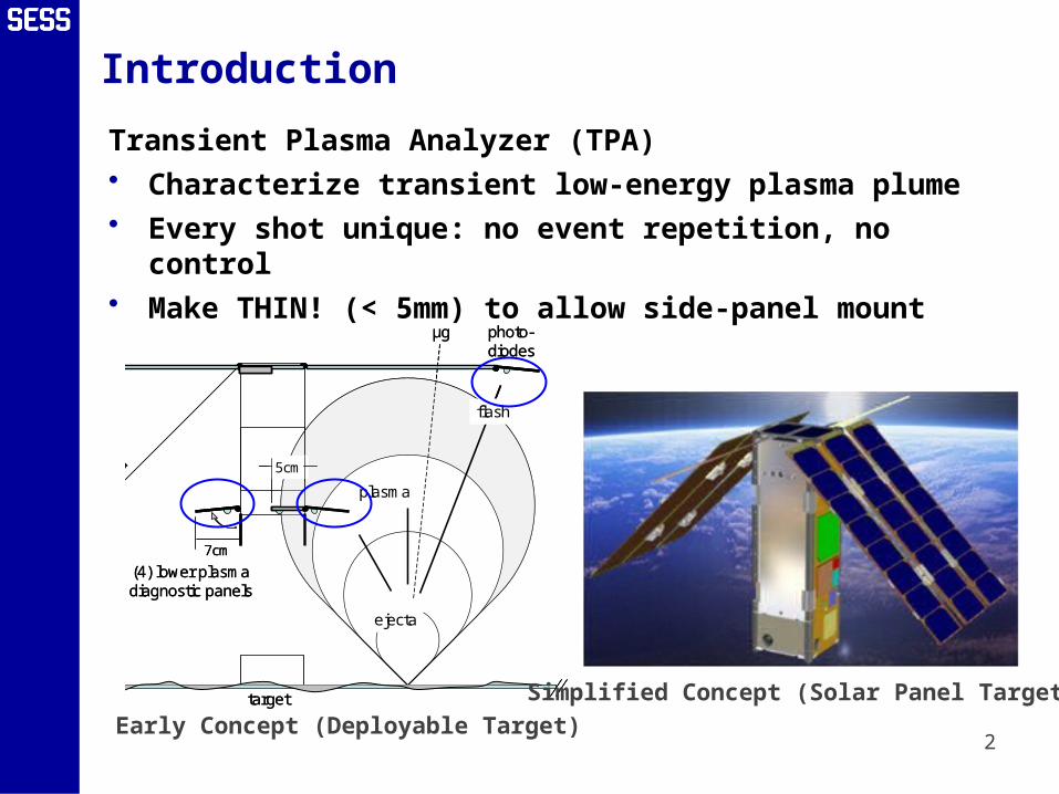
Introduction
Transient Plasma Analyzer (TPA)• Characterize transient low-energy plasma plume• Every shot unique: no event repetition, no control• Make THIN! (< 5mm) to allow side-panel mount
2
(4) lower plasmadiagnostic panels
(4) upper plasmadiagnostic panels
7cm
5cm
target
ejecta
μg
flash
plasma
photo-diodes
(4) lower plasmadiagnostic panels
(4) upper plasmadiagnostic panels
7cm
5cm
target
ejecta
μg
flash
plasma
photo-diodes
Early Concept (Deployable Target)
Simplified Concept (Solar Panel Targets)

Build on previous success!
3
-+
RPA GroundedBNC
Vacuum Air
n/c
Vout
Vcom
V+
Scope
V-
±100V
±50V
-10V
Vrep
Vthr
Vsup
D. Lauben, 2010-Aug-03
RPA’s share vacuum-side voltage as follows:1.Like charge species share Vrep, Vsup2.Like charge species may share Vthr3.All RPA’s share V+ and V- power
FloatedSMA
Wall
-+
RPA GroundedBNC
Vacuum Air
n/cn/c
Vout
Vcom
V+
Scope
V-
±100V
±50V
-10V
Vrep
Vthr
Vsup
D. Lauben, 2010-Aug-03
RPA’s share vacuum-side voltage as follows:1.Like charge species share Vrep, Vsup2.Like charge species may share Vthr3.All RPA’s share V+ and V- power
FloatedSMA
Wall
• Simple Retarding Potential Analyzer• Concept to working unit in < 30 days• 1st unit fab: ~3 days; 2nd unit: 1 day!
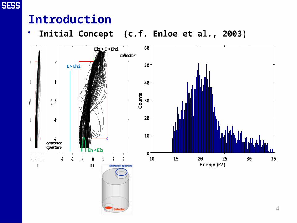
Introduction• Initial Concept (c.f. Enloe et al., 2003)
4
-3 -2 -1 0 1 2 3
-2
-1
0
1
2
Electron Trajectories, Vbias = -275 V
mm
mm
10 15 20 25 30 350
10
20
30
40
50
60
Energy (eV)
Co
un
ts
Energy Passband (20 eV)
-3 -2 -1 0 1 2 3
-2
-1
0
1
2
Electron Trajectories, Vbias = -275 V
mm
mm
E > Ehi
En < Elo
collector
entranceaperture
Elo < E < Ehi

Improvement
• Revised “C” Aperture (best efficiency)
5
(comsol model)

3D Trajectory Simulation• Accepted particles
6
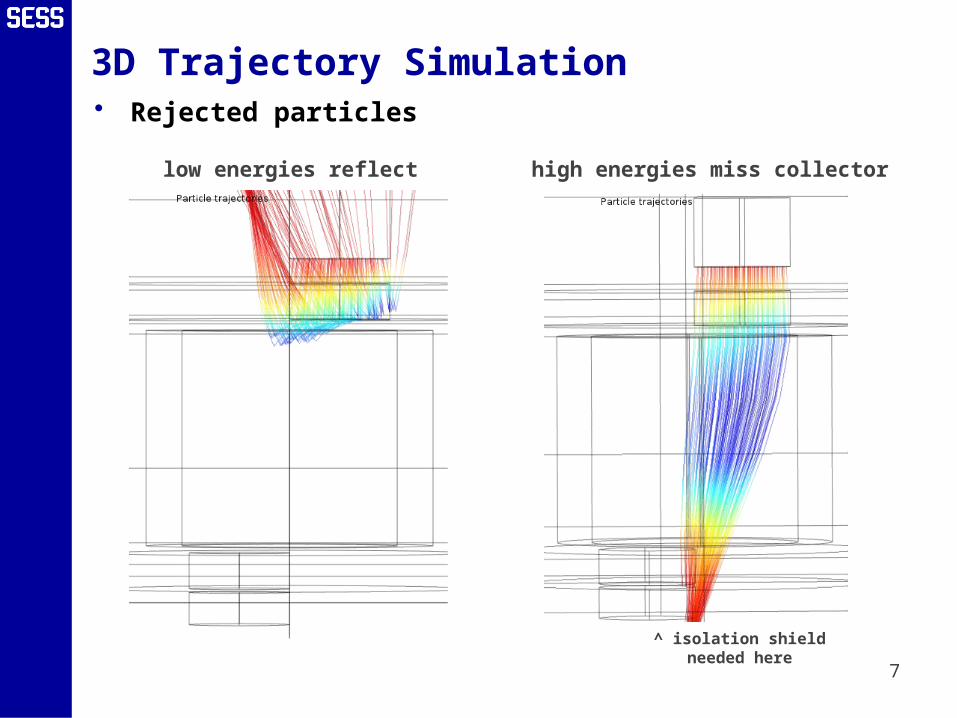
3D Trajectory Simulation• Rejected particles
7
low energies reflect high energies miss collector
^ isolation shieldneeded here
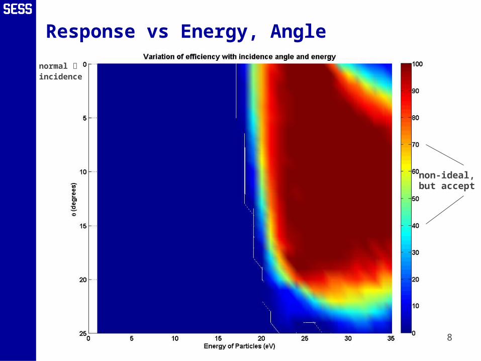
Response vs Energy, Angle
8
normal incidence
non-ideal,but accept
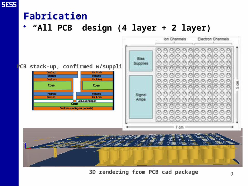
Fabrication• “All PCB” design (4 layer + 2 layer)
93D rendering from PCB cad package
Cu (Gnd)
Cu (Gnd)
Prepreg
Prepreg
Core
Core
Core
Cu (Gnd)Prepreg
Cu (Gnd)
Cu (Bias) Cu (Bias)
Cu (Collector pad)
Prepreg
Cu (for mounting components)
PCB stack-up, confirmed w/supplier
TPA Design Summary
• “All PCB” flat-panel Transient Plasma Analyzer• c.f., AFIT: MESA, iMESA (ISS/MISSE-7), PCBSAT
• 12x12 mm-scale micro-electrostatic analyzers• (8) clusters of 9 cells/cluster, for (8) e- energy bands• (8) clusters of 9 cells/cluster, for (8) ion energy bands
• Commandable bias voltage for energy selection• Ex: unbiased target: V = 0.5, 1, 2, 5, 10, 20, 50, 100+• Ex: biased target: V = 5, 10, 20, 50, 100, 200, 500+
• Option (at fabrication) for extreme bandwidth• Default: BW > 10 MHz using standard COTS electronics• Option: BW > 1 GHz using latest UWB high-fT discretes
• Data as raw, or onset + time-over-threshold mode
10

TPA Development Plan
11
• Ground Tests (Stanford)• Calibrate using standard low-energy e-, ion sources• Simulate HVI events via nanosecond, microjoule laser• Plasma production, RF emission, Sensor Response
• Ground HVI Experiments (LASP)• Measure hypervelocity (>20 km/s), femtogram projectiles• Verify computer models: Plasma, RF, Chamber, Sensors
• Prototype Test Flight• Low-earth orbit plasma environment
• Science Missions!• True in-situ micrometeoroid distribton
Accurate Chamber Effects Model


