
®
Instruments
Spectrum
analyzer
HM5011HM5010
EN
GL
ISH
4
S-5
01
0-0
01
0
09
JU
N 1
99
8
SERVICE-MANUAL HM5011/5010

2Subject to change without notice
HM5010/5011
Service ManualAdjustment ProcedureCircuit Diagrams
Alignment Procedure for HM5010/HM 5011 ......... 5A Control and Adjustment of
Supply Voltages ............................................... 5B Final Alignment - Tuner ..................................... 6C Alignment - IF-Unit ........................................... 6D Linearity of Frequency Display ......................... 7
HM5010 XY-board ........................................... 10Tuner ............................................................... 11Tracking-Generator .......................................... 12
E Alignment of HM5011 Tracking Generator ...... 13
Tracking-Generator ................................................. 15Tuner RA-Board ...................................................... 16Tuner RB-Board ...................................................... 17IF-Amplifier ............................................................. 18Main board ............................................................. 19X-Y Board ............................................................... 20FC-Board ................................................................ 21PA-Board ................................................................ 22CRT-Board .............................................................. 23Power supply Board ............................................... 24RA-Board ................................................................ 25Tracking-Generator ................................................. 26RB-Board ................................................................ 27Main board ............................................................. 28Main board ............................................................. 29XY-Board ................................................................. 30XY-Board ................................................................. 31FC-Board ................................................................ 32FC-Board ................................................................ 33PA-Board ................................................................ 34CRT-Board .............................................................. 35PS-Board ................................................................ 36PS-Board ................................................................ 37PS-Board ................................................................ 38Block Diagram HM5010/HM5011 .......................... 39

Subject to change without notice3
SPECTRUM ANALYZER
This HO500 computer interface offers the facility to transfer a calibrated frequencyspectrum from any HAMEG spectrum analyzer to a PC. The HO500 interface is a8 bit ISA BUS card installed in the PC, which transfers data via an interface cable.The software supplied allows a hard copy print out (including parameters) of thefrequency spectrum, in Windows Format. Signal aquisition occurs 2 to 3 times per
second.The picture consists of 10 bit vertical by approx 3600 point horizontal display. The PCmonitor display is in SVGA Format with 800 x 600 pixels. For comparisonmeasurements, a previosly stored reference curve can be recalled. The softwaresupplied works under Windows 3.1, 3.11 and WIN95. A simple XY analog output isrequired to connect the HO500 to the spectrum analyzer.
HO500 Computer Interface for HAMEG Spectrum Analyzer
Frequency Range 0.15MHz - 1050MHz.
4½ Digit Display (Center & Marker Frequency, 0.1MHz resolution)
–100 to +13dBm Amplitude Range, 20kHz, 400kHz and Video-Filter
Tracking-Generator (HM5011 only):
Frequency range: 0.15MHz - 1050MHz.
Output Voltage: +1dBm to –50dBm (50ΩΩΩΩΩ).
Evolution of the original HM5005/HM5006 has led to the new HM5010/
HM5011 Spectrum Analyzer/Tracking Generator which now extendsoperation over 1 GHz (frequency range 0.15 to 1050 MHz). Both fine andcoarse center frequency controls, combined with a scanwidth selectorprovide simple frequency domain measurements from 100 kHz/div. to 100MHz/Div.. Both models include a 4½digit numeric LED readout that canselectively display either the center or marker frequency. The HM5011
includes a tracking generator.The HM5010/5011 offer the same operation modes as the HM5005/5006.
The instruments are suitable for pre-compliance testing during developmentprior to third party testing. A near-field sniffer probe set, HZ530, can be usedto locate cable and PC board emission "hot spots" and evaluate EMC problems
at the breadboard and prototype level. The combination of HM5010/5011 withthe HZ530 is an excellent solution for RF leakage/radiation detection, CATV/
MATV system troubleshooting, cellular telephone/pocket pager test and EMC
diagnostics. There is an optional measurement output for a PC which makesdocumentation of results easy and affordable with the HO500 Interface.
Specifications
Frequency
Frequency range: 0.15MHz to 1050MHz (-3dB)Center frequency display accuracy: ±100kHzMarker accuracy: ±(0.1% span + 100kHz)Frequency display res.: 100kHz (4½ digit LED)Frequency scanwidth: 100kHz/div. to 100MHz/div.
in 1-2-5 steps and 0Hz/div. (Zero Scan)Frequency scanwidth accuracy: ±10%Frequency stability: better than 150kHz / hourIF Bandwidth (-3dB): Resolution: 400kHz and20kHz; Video-Filter on: 4kHzSweep rate: 43Hz
Amplitude
Amplitude range: -100dBm to +13dBmScreen display range: 80dB (10dB / div.)Reference level: -27dBm to +13dBm
(in 10dB steps)Reference level accuracy: ±2dBAverage noise level: -99dBm (20kHz BW)Distortion: <-75dBc; 2nd and 3rd harmonic
3rd order intermod.: -70dBc(two signals >3MHz apart)
Sensitivity: <5dB above average noise levelLog scale fidelity: ±2dB (without attn.) Ref.: 250MHzIF gain: 10dB adjustment range
Input
Input impedance: 50ΩInput connector: BNCInput attenuator: 0 to 40 dB (4 x 10dB steps)Input attenuator accuracy: ±1dB/10dB stepMax. input level: +10dBm, ±25VDC (0dB attenuation)
+20dBm (40dB attenuation)
Tracking Generator
Output level range: -50dBm to +1dBm(in 10dB steps and var.)
Output attenuator: 0 to 40dB (4 x 10dB steps)Output attenuator accuracy: ±1dBOutput impedance: 50Ω (BNC)Frequency range: 0.15MHz to 1050MHzFrequency response: ±1.5dBRadio Frequency Interference (RFI): <20dBc
Divers
AM-Demodulator output for head-sets.Permissible load impedance >8Ω
General
Display: CRT. 6 inch, 8 x 10 div. intern. graticuleTrace rotation: Adjustable on front panelLine voltage: 115 / 230V ±10%, 50-60HzPower consumption: approx. 20WOperating ambient temperature: 0°C..+40°CProtective system: Safety Class I (IEC 1010-1)Weight: approx. 7kgCabinet: W 285, H 125, D 380 mm
Subject to change without notice 5/96
Spectrum Analyzer HM5010 / HM5011
Accessories supplied: Line Cord, Operators Manual. Optional accessories, 50ΩΩΩΩΩ-feedthrough termination HZ22
Viewing Hood HZ47, Near Field Probe Set HZ530, Carrying Case HZ96-2, Transient Limiter HZ560

4Subject to change without notice
The HZ530 is the ideal toolkit for theinvestigation of RF electromagnetic
fields. It is indispensable for EMI pre-
compliance testing during productdevelopment, prior to third party testing.The set includes 3 hand-held probes
with a built-in pre-amplifier covering thefrequency range from 100kHz to over 1000
MHz.The probes - one magnetic field probe,
one electric field probe, and one high
impedance probe - are all matched to the50Ω inputs of spectrum analyzers or RF-
receivers. The power can be suppliedeither from batteries, Ni-Cads or through apower cord directly connected to anHM5010/HM5011 series spectrumanalyzer.
Signal feed is via a 1.5m BNC-cable.When used in conjuction with a spectrumanalyzer or a measuring receiver, theprobes can be used to locate and qualify
EMI sources, as well as evaluate EMCproblems at the breadboard andprototype level. They enable the user toevaluate radiated fields and perform shield
effectiveness comparisons. Mechanicalscreening performance and immunity testson cables and components are easilyperformed.
The H-Field Near-Field ProbeThe H-Field probe provides a voltage to
the connected measurement system whichis proportional to the magnetic radiofrequency (RF) field strength existing at theprobe location. With this probe, circuit RFsources may be localized in close proximityof each other. The H-field will decrease asthe cube of the distance from the source. Adoubling of the distance will reduce the H-field by a factor of eight (H = 1/d³); where dis the distance.
In the actual use of the H-field sensor oneobserves therefore a rapid increase of theprobe’s output voltage as the interferencesource is approached. While investigating acircuit board, the sources are immediatelyobvious. It is easily noticed which component(i.e. IC) causes interference and which doesnot. In addition, by use of a spectrum analyzer,the maximum amplitude as a function offrequency is easily identified. Therefore, onecan eliminate early in the development com-ponents which are not suitable for EMCpurposes. The effectiveness of countermeas-ures can be judged easily. One can inves-tigate shields for "leaking" areas and cablesor wires for conducted interference.
The High-Impedance ProbeThe high-impedance probe (Hi-Z) permits
the determination of the radio frequencyinterference (RFI) on individual contacts orprinted circuit traces. It is a direct-contactprobe. The probe is of very high impedance
Specifications
Frequency
Frequency range: 0.1MHz to 1000MHz(lower frequency limit
depends on probe type)Output impedance: 50 ΩOutput connector: BNC-jackInput capacitance: 2pF
(high imped. probe)Max. Input Level: +10dBm
(without destruction)1dB-compression point: -2dBm
(frequency range dependent)DC-input voltage: 20V max.Supply Voltage: 6V DC
4 AA size batteriesSupply-power of HM5010/5011
Near Field Sniffer Probes HZ 530
Supply Current: 8mA (H-Field Probe)15mA (E-FieldProbe)24mA(High imp.Probe)
Probe Dimensions: 40x19x195mm (WxDxL)Housing: Plastic; (electrically
shielded internally)
Package contents: Carrying case1 H-Field Probe1 E-Field Probe1 High Impedance Probe1 BNC cable (1.5m)1 Power Supply Cable
(Batteries or Ni-Cads are not included)
(near the insulation resistance of the printedcircuit material) and is loading the test pointwith only 2 pF (80Ω at 1 GHz). Thereby onecan measure directly in a circuit withoutsignificantly influencing the relationships inthe circuit with the probe.
One can, for example, measure the quan-titative effectiveness of filters or otherblocking measures. Individual pins of ICs canbe identified as RFI sources. On printedcircuit boards, individual problem tracks canbe identified. With this Hi-Z probe individualtest points of a circuit can be connected tothe 50Ω impedance of a spectrum analyzer.
The E-Field Monopole ProbeThe E-field monopole probe has the
highest sensitivity of the three probes. It issensitive enough to be used as an antennafor radio or TV reception. With this probe theentire radiation from a circuit or an equipmentcan be measured. It is used, to determine theeffectiveness of shielding measures. Withthis probe, the entire effectiveness of filterscan be measured by measuring the RFI whichis conducted along cables that leave the equip-ment and may influence the total radiation.In addition, the E-field probe may be usedto perform relative measurements for certi-fication tests. This makes it possible to applyremedial suppresion measures so that any re-qualification results will be positive. In addition,pre-testing for certification tests may be per-formed so that no surprises are encounteredduring the certification tests.
SC
ALE
= 1
0dB
/DIV
.
SC
ALE
= 1
0dB
/DIV
.
Frequency Response E-Field Probe (typical) Frequency Response H-Field Probe (typical)
SC
ALE
= 1
0dB
/DIV
.
Frequency Response High Impedance Probe(typical)
EMC-MEASUREMENT EQUIPMENT

Subject to change without notice5
Attention! The opening of covers or removal of parts is likely to expose live parts and accessible terminalswhich can be dangerous to life. Maintenance, service and alignment should be carried out by qualifiedpersonnel only, which is acquainted with the danger involved.
When aligning the HM5010/5011 it is assumed that all sub-assemblies of the instrument are completely pretested andworking correctly. The tuner, IF-unit, and tracking generator should be pre-aligned. When aligning a HM5010, a separatetracking generator unit must be available and connected to the HM5010 for some specific adjustments.Prior to the alignment procedure, the instrument must warm up for 60 minutes.All adjustments are carried out by means of a plastic screw driver or a ceramic adjustment tool.
The alignment is divided into the following steps:A Checking of supply voltages D Linearity alignmentB Alignment of the tuner E Tracking generator alignmentC Alignment of the IF-unit F Check of overall adjustment
The numbering system is related to the respective pictures. Screen shots are designated as PIC1 HF-Synthesizer 100 kHz to 1000 MHz, i.e. HM 81332 BNC cable, BNC T-connector, 2 x 10dB attenuator 50 Ohm1 Voltmeter i.e. HM 8011-3
A Control and Adjustment of Supply Voltages
adjust: 12V to an accuracy of ±0.1V via Trimpot 4 PIC 1adjust: minimum brightness via Trimpot 2 PIC 1adjust: maximum brightness via Trimpot 3 PIC 1adjust: astigmatism via Trimpot 1 PIC 1
check: –12V tolerance ± 0.2Vcheck: +12V tolerance ± 0.1Vcheck: +5V tolerance ± 0.2Vcheck: –5V tolerance ± 0.2Vcheck: +38V tolerance ± 1Vcheck: +138V tolerance ± 1V
4
CRT-BoardPIC 1. PS-Board Instrument Rear Side
3 2 1
1 +138V2 +38V3 GND4 +5V5 +12V6 -12V
1
PIC 2. XYF-Board (partial)
1
The corresponding voltage test points to check direct voltage canbe measured at the measuring connector strip (see PIC 2).
Basic adjustment:When Y-pos. knob is snapped in on front board, adjust beamapprox. 2 mm below bottom graticule line via R801.
Alignment Procedure for HM5010/HM 5011
6Subject to change without notice
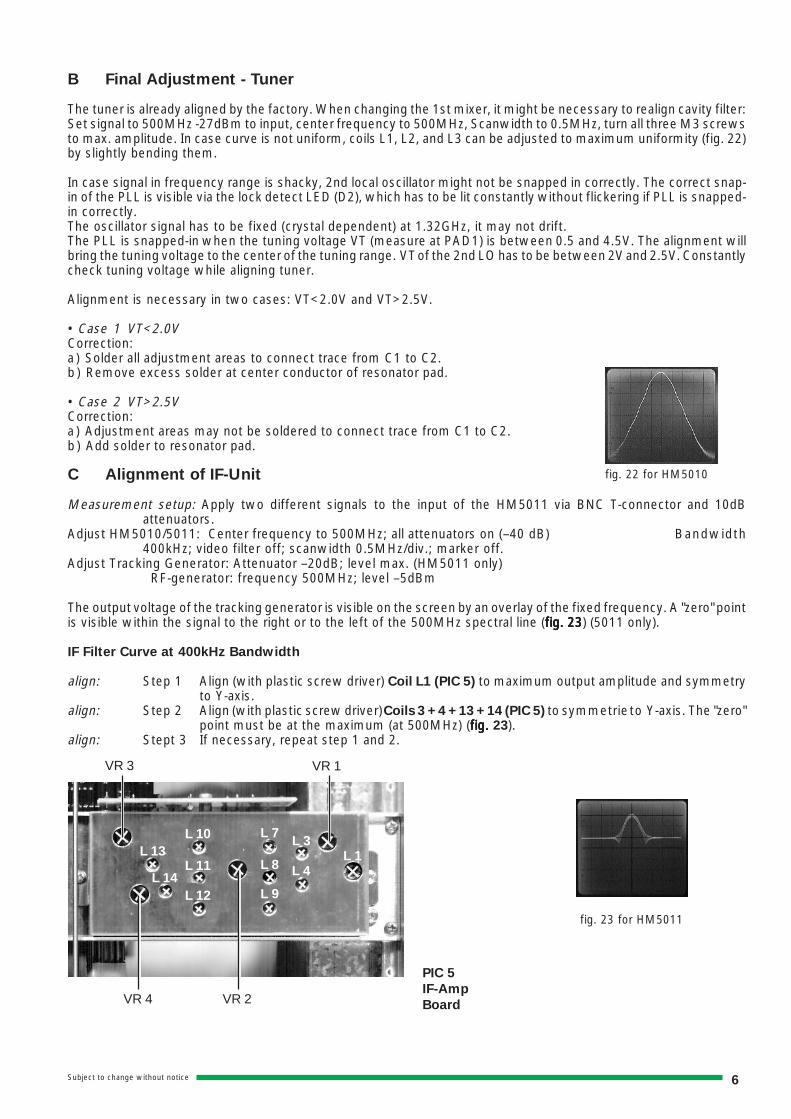
fig. 22 for HM5010
L 11
L 10
L 12
L 8
L 7
L 9
L 13
L 14L 4
L 3L 1
VR 3
VR 4 VR 2
VR 1
PIC 5
IF-Amp
Board
B Final Adjustment - Tuner
The tuner is already aligned by the factory. When changing the 1st mixer, it might be necessary to realign cavity filter:Set signal to 500MHz -27dBm to input, center frequency to 500MHz, Scanwidth to 0.5MHz, turn all three M3 screwsto max. amplitude. In case curve is not uniform, coils L1, L2, and L3 can be adjusted to maximum uniformity (fig. 22)by slightly bending them.
In case signal in frequency range is shacky, 2nd local oscillator might not be snapped in correctly. The correct snap-in of the PLL is visible via the lock detect LED (D2), which has to be lit constantly without flickering if PLL is snapped-in correctly.The oscillator signal has to be fixed (crystal dependent) at 1.32GHz, it may not drift.The PLL is snapped-in when the tuning voltage VT (measure at PAD1) is between 0.5 and 4.5V. The alignment willbring the tuning voltage to the center of the tuning range. VT of the 2nd LO has to be between 2V and 2.5V. Constantlycheck tuning voltage while aligning tuner.
Alignment is necessary in two cases: VT<2.0V and VT>2.5V.
• Case 1 VT<2.0VCorrection:a ) Solder all adjustment areas to connect trace from C1 to C2.b ) Remove excess solder at center conductor of resonator pad.
• Case 2 VT>2.5VCorrection:a ) Adjustment areas may not be soldered to connect trace from C1 to C2.b ) Add solder to resonator pad.
C Alignment of IF-Unit
Measurement setup: Apply two different signals to the input of the HM5011 via BNC T-connector and 10dBattenuators.
Adjust HM5010/5011: Center frequency to 500MHz; all attenuators on (–40 dB) Bandwidth400kHz; video filter off; scanwidth 0.5MHz/div.; marker off.
Adjust Tracking Generator: Attenuator –20dB; level max. (HM5011 only) RF-generator: frequency 500MHz; level –5dBm
The output voltage of the tracking generator is visible on the screen by an overlay of the fixed frequency. A "zero" pointis visible within the signal to the right or to the left of the 500MHz spectral line (fig. 23fig. 23fig. 23fig. 23fig. 23) (5011 only).
IF Filter Curve at 400kHz Bandwidth
align: Step 1 Align (with plastic screw driver) Coil L1 (PIC 5) to maximum output amplitude and symmetryto Y-axis.
align: Step 2 Align (with plastic screw driver) Coils 3 + 4 + 13 + 14 (PIC 5) to symmetrie to Y-axis. The "zero"point must be at the maximum (at 500MHz) (fig.fig.fig.fig.fig. 23).
align: Stept 3 If necessary, repeat step 1 and 2.
fig. 23 for HM5011

Subject to change without notice7
IF Filter Curve at 20kHz Bandwidth (HM5010)
align: Step 1 Align (with plastic screw driver) Coils L7+8+9+10+11+12 until "zero" point is exactly centeredat 500MHz (as with 400kHz Bandwidth).Watch for symmetry of Filter Curve.
IF Filter Curve at 20kHz Bandwidth (HM5011)
Pre-Alignment: Remove T-connector. Connect tracking generator module directly to the input of the HM5011. Turnoff attenuators on tracking generator module and on HM5011 (0 dB). The output voltage of the tracking generatormodule is now visible as horizontal line (with slight ripple).
adjust: Step 1 Adjust (with plastic screw driver) Coils 7 + 8 + 9 + 10 + 11 + 12 to maximum screen heightof displayed output voltage. Add attenuators of HM5010/5011 as soon as "line" has reached themiddle of the screen (–30 dB).
adjust: Step 2 This alignment has to be performed repeatedly in order to optimize settings.
Fine Alignment: Connect BNC-T-connector again as in the beginning of the IF alignment. Set attenuator of trackinggenerator module to –20dB, scanwidth to 0.5 MHz/div. If necessary, re-adjust center frequency(adjust 500MHz spectral line to screen center). "Zero" point is now visible to the right or to theleft of screen center (amplitude maximum) (fig.fig.fig.fig.fig. 24).
adjust: Step 1 Align (with plastic screw driver) Coils L7+8+9+10+11+12 until "zero"point reaches maximum. Watch for symmetry of Filter Curve.
adjust: Step 2 This alignment has to be performed repeatedly in order to optimizesettings.
IF Gain - Adjustment of different Bandwidths
Set scanwidth to 0.2MHz/div. Switch bandwidth repeatedly between 400kHz and 20kHz. The distance between theoutput voltage (line) of the tracking generator and tge 400MHz amplitude may not vary. If the amplitude values donot match exactly, adjust by means of R-trimmer VR2 (PIC5)VR2 (PIC5)VR2 (PIC5)VR2 (PIC5)VR2 (PIC5).
Linearity of IF-Amplifier Gain
The linearity of the IF-amplifier gain has to be checked through the entire display range. Apply a 400MHz (-27dBm)signal directly to the input of the HM5010/5011. Adjust scanwidth to 5MHz/div, release attenuator switched (0 dB),select filter bandwidth of 400kHz. The spectral line should reach the upper screen edge. Use attenuators to reducesignal in 10db steps, whereby each individual attenuation step has to reduce the level by 10dB ±1dB. In case deviationis as follows:
- A the drop of the individual attenuation steps is larger than 10dB ± 1dB, or
- B the drop of the individual attenuation steps is smaller than 10dB ±1dB, the linearity of the attenuators has to beadjusted as follows:
Set attenuator to -40dB. Adjust spectral line exactly to -40dB (center line) via VR1, VR3, VR4. Then set attenuatorsback to 0dB und adjust spectral line by means of trimpots VR802A and VR801 (XY board) to zero point and baseline to bottom graticule line. This procedure has to be repeated until the settings at -40dB and 0dB are correct.
D Linearity of Frequency Display
Settings for HM5010/5011: Center frequency at 500MHz; all attenuator switches released; filter bandwidth400kHz; video filter off; scanwidth to 100MHz/div.; marker off.
Measurement Setup: Apply signal of 500MHz –27dBm to input of HM 5010/5011.
Check: Basic setting: The HM5010/5011 has to be adjusted that the noise level touches the bottom graticuleline. The spectral line of 500MHz -27dBm reaches the top graticule line and is situated in the center ofthe screen. Adjust 500MHz spectral line exactly to screen center via X-pos knob (on front of the unit).
Check: Upper frequency limit: Check if frequency of minimum 1050 can be set as center frequency.
fig. 24

8Subject to change without notice
fig. 7
Adjust HM5010/5011 to basic setting (see above). Apply input signal of 100MHz, level +7dBmOverriding the input allows for the harmonics of the input signal to become visible (fig. 7)fig. 7)fig. 7)fig. 7)fig. 7). Thissimplifies the adjustment of individual spectral lines in horizontal direction.
adjust: Spectral line at 400MHzTurn X-ampl. knob on front of instrument to have the 4 spectral lines matched withthe corresponding graticule lines on the screen(fig. 8fig. 8fig. 8fig. 8fig. 8).
adjust: Spectral line at 100MHzWith Trimpot RV171 align to match this spectral line with the correspondinggraticule line on the screen (fig. 9fig. 9fig. 9fig. 9fig. 9).
adjust: Zero PeakWith Trimpot RV173 align to match this spectral line with the correspondinggraticule line on the screen (fig. 9fig. 9fig. 9fig. 9fig. 9).
adjust: Spectral line at 600-1000MHzWith Trimpot RV186 adjust to match 700MHz to the correct graticule line.
adjust: Spectral line at 800 MHz;With Trimpots RV181 + RV183 for 900MHz and RV197 for 1000MHz (PIC 3)adjust to match this spectral line with the corresponding graticule line on thescreen.
adjust: Beam lengthWith Trimpot RV101 adjust beam to end approx. 1mm beyond the right CRTboundary (graticule) (Fig. 11 Fig. 11 Fig. 11 Fig. 11 Fig. 11 - base line too short) (Fig. 10 Fig. 10 Fig. 10 Fig. 10 Fig. 10 - 300 to 1000MHz spectral lines not correct )
Set Trimpot RV113 that frequency will notdisplay below 990MHz when center frequencyis set to lowest frequency
RV 173
RV 171
RV 197
RV 186
RV 181
RV 183
RV 149
RV 112
RV 101
PIC 3 - MB-Board
fig. 11
fig. 8
fig. 9
fig. 10
RV113

Subject to change without notice9
VR 3
L 11
L 10
L 12
L 8
L 7
L 9
L 13
L 14L 4
VR 4
L 3L 1
RV 113
RV 101
RV 173
RV 171
RV 197
RV 186
RV 181
RV 183
RV 149
RV 112
PIC 3 - Main-Board
Adjust Marker.Settings on HM5010/5011: Center frequency to 500MHz, all attenuators in off position, filter bandwidth to 400kHz,video filter off.Scanwidth to 100MHz, Marker on.Signal 100MHz +7dBm.Adjust Marker to 500MHz display and set to 500MHz mark on screen via RV149 (PIC 4).Turn Marker left to max. and adjust to 990MHz via RV112.
VR 2
VR 1

10Subject to change without notice
RV
802
A
RV
801
1 +138V2 +38V3 GND4 +5V5 +12V6 -12V
1
XY-Board

Subject to change without notice11
Tuner
M3
Scr
ews
Ca
vit
y -
Fil
ter
M3
Scr
ews
Ca
vit
y -
Fil
ter
1st
Mix
erM
PAD
1C
1 C
2

12Subject to change without notice
MPA
D2
C68
C69
RV
4R
V3
Tracking-Generator
Subject to change without notice13
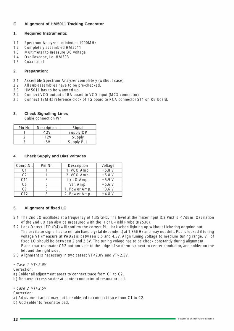
E Alignment of HM5011 Tracking Generator
1. Required Instruments:
1.1 Spectrum Analyzer - minimum 1000MHz1.2 Completely assembled HM50111.3 Multimeter to measure DC voltage1.4 Oscilloscope, i.e. HM3031.5 Coax cabel
2. Preparation:
2.1 Assemble Spectrum Analyzer completely (without case).2.2 All sub-assemblies have to be pre-checked.2.3 HM5011 has to be warmed up.2.4 Connect VCO output of RA board to VCO input (MCX connector).2.5 Connect 12MHz reference clock of TG board to RCA connector ST1 on RB board.
3. Check Signalling Lines
Cable connection W1
Pin Nr. Description Signal1 -12V Supply OP2 +12V Supply3 +5V Supply PLL
4. Check Supply and Bias Voltages
Comp.Nr. Pin Nr. Description VoltageC1 1 1. VCO Amp. +5.8 VC2 1 2. VCO Amp. +5.8 VC11 3 fix LO Amp. +5.9 VC6 5 Var. Amp. +5.6 VC9 3 1. Power Amp. +3.6 VC12 3 2. Power Amp. +4.8 V
5. Alignment of fixed LO
5.1 The 2nd LO oscillates at a frequency of 1.35 GHz. The level at the mixer input IC3 Pin2 is -17dBm. Oscillationof the 2nd LO can also be measured with the H or E-Field Probe (HZ530).
5.2 Lock-Detect LED (D4) will confirm the correct PLL lock when lighting up without flickering or going out.The oscillator signal has to remain fixed crystal dependent) at 1.35GHz and may not drift. PLL is locked if tuningvoltage VT (measure at PAD2) is between 0.5 and 4.5V. Align tuning voltage to medium tuning range. VT offixed LO should be between 2 and 2.5V. The tuning volage has to be check constantly during alignment.Place coax resonator CR2 bottom side to the edge of soldermask next to center conductor, and solder on theleft and the right side.
5.3 Alignment is necessary in two cases: VT<2.0V and VT>2.5V.
• Case 1 VT<2.0VCorrection:a ) Solder all adjustment areas to connect trace from C1 to C2.b ) Remove excess solder at center conductor of resonator pad.
• Case 2 VT>2.5VCorrection:a ) Adjustment areas may not be soldered to connect trace from C1 to C2.b ) Add solder to resonator pad.

14Subject to change without notice
6. Control of fixed LO-Level
6.1 To check 2nd LO-level, cap C20 (22pF) has to be removed and 50Ohm Coax-cable has to be connected to -13dB attenuator of output. Connect other end of coax cable with adequate test analyzer.
6.2 Adjust test analyzer to 1.35 GHz center frequency; the LO-level to be measured has to be -17dBm (±1 dB)(consider attenuation of cable).
6.3 If cap is not removed and coax cable is connected parallel to mixer to the VCO-branch, a level of approx. -24dBm (±1dB) should be measured due to decreased load resistance.
7. Check of VCO
7.1 Adjust HM5011 to Zero Scan, center frequency to 500MHz.7.2 Remove Cap C14 (22pF), connect one side to attenuator output, other side stand up in the air.7.3 Connect Cap side sticking up in the air to center conductor of 50 Ohm cable. Solder shielding of cable directly
next to Cap to ground. Connect other end of Cap to Analyzer input (i.e. Advantest R3361A). Start 1.35GHz -Stop 2.35GHz reference level: 0dBm.
7.4 VCO signal which can be observed on the test analyzer has to shift according to center frequency (tuningvoltage). Tuning range has to be at least from 1350 to 2350 Mhz. continuously and without interruption. Itshould not go under absolute level of +7dBm (coax cable of 1 mtr. has 1-2 dB of attenuation at 2GHz). Levelhas to be between +7 dBm and +10 dBm.
7.5 Connect coax cable parallel to 1st mixer to VCO-branch. A level of +5 dBm to +8 dBm due to decreased loadresistance over frequency band.
8. Check of Attenuators:
8.1 Set -30dB attenuation to Tuner and to 0dB attenuation to TG.8.2 Set Center Frequency to 500MHz, 100MHz/Div. span.8.3 Connect tracking generator to tuner input.8.4 TG-line has to be visible.8.5 Switch on additional attenuators. Attenuation for each attenuator switch has to be 10dB (±1 dB)
9. TG Level Adjustment:
9.1 Connect TG to reference analyzer.9.2 Set HM5011 to Zero Scan and 500MHz Center Frequency.9.3 Release all attenuator buttons of TG (0-dBm) and turn TG-level to maximum.9.4 Adjust amplitude to +1dBm with Pot RV4 on TG.9.5 turn TG-level to minimum.9.6 Adjust amplitude to -10dBm with Pot RV3 on TG.9.7 Amplitude has to be adjustable now between +1dB and -10dB.
10. Final Check
10.1 Position of TG-level has to align in both bandwidths (400kHz and 20kHz). If necessary, align with IF-Amp.10.2 TG-level knob has to be adjustable from +1 to -10dBm.

Subject to change without notice15
Tracking-Generator
16Subject to change without notice
Tuner RA-Board
Subject to change without notice17
Tuner RB-Board

31Subject to change without notice
Dat
e:
M
ay 5
, 199
4Sh
eet
2
of
8
Size
Doc
umen
t Num
ber
REV
BIF
5005
.SCH
Title
IF A
MP
HM
5005
/6
HA
MEG
INST
RUM
ENTS
GER
MA
NY
GN
D+1
2V
1 1
2 2
3 3
4 4
5 5
6 6
KA11
01
+12V
L110
110
0u
L110
210
0u
IF P
CB
R5 220R
C9 0.1u
R8 221R
+12V
IF A
MP
IF IN
FRO
M T
UN
ER2n
d IF
OU
T
C10
10n
F3 RF2
R6 10K0
R9 3K32
R7 10K0
C11
82p
C5 39p
C6 82p
T1 BC54
7
4.7V
=
C8 10n
+5V
BWVID
GN
D+5
V
VID
EO S
IGN
AL
BW
P803
S.3
TO X
YF P
CB
1 2 3 4KA11
02G
ND
IF G
AIN
+12V
+5V
TO A
L (R
F U
NIT
)KA
901
S.1
IF G
AIN +1
2V +
5V
R3 2K21
L20.
82u
C7
33p
R4 470R
C12
33p
R2 47R5
XT1
27.1
25M
Hz
F4 RF2
C13
220p
C14
220p
T2 BF96
1
C4 8p2
F1 RF3
VR1
200R25
0mV
R1 100k
C3
22p
30.0
MH
z
C1 8p2
C2 47p
IF1
2
R10
2.2k
TUN
ER G
AIN
COM
P.
R18
470k
R15
221R
C29
1p8
C26
0.1u
L5 15u
F12
RF2
R32
100R
R34
2K2
R35
2K21
NTC
+8.8
V
R33
180R
C41
22u
1 2 3 4 5 11 12 13 15 16 17 18 19 20U F 1 4
8
VCC
6
G 7 9
IC1
MC3
356P
R31
4K75
C40
180p
VR3
500R
GA
IN
OVE
RALL
R28
470K
R30
3K32
F13 RF
2
F14
RF2
C38
180p
C32 1p8
C31
270p
C39
10n
C27 10
nC2
812
0p
F10 RF
2
C30
270p
C25 10n
R17
47R5
VR2
50K
500m
Vpp
R21
100kD1
1N41
48
D2
1N41
48
T3 BC55
7
C20
270p
C18
120p
R11
4K75 F19 RF
2
C19
1p8
C15 22p
C22
1p8 C2
312
0p
C21
270p
C24
10n
F9 RF2
F7 RF2
R13
100k
R16
181R
C34 10
n
C33
120p
T4 BF96
1
11V=
0.7V
pp
R14
220R
C37
0.1u
R23
22K1
R22
4K75
F11 RF
2
D3
1N41
48
D4
1N41
48
R27
150k
T6 BF96
1
R26
100K
C36
330p
R29
47R5
400m
Vpp
>2Vp
p
R24
100R
R36
332R
C43
0.1u
200m
Vpp
7.6V
=
R37
3K92
C44
22p
C42
10n
R38
22K
R39
2K21
NTC
C35
10n
VR4
100K
IF G
AIN
RAN
GE
R25 18
0R
R20
47K5
T5 BC54
7
NTC
C16
0.1u
C17
0.1u
R19
4K75
R40
2K21
+12V
CD1
1nF
BW
0V(2
50 k
Hz)
CD2
1nF
+8V(
12.5
kH
z)
IF G
AIN
FRO
M A
TTEN
. RF
UN
IT S
.1
CD3
1nF
VID
EO S
IGN
AL
VIDCD
41n
F
IF-Amplifier

Subject to change without notice32
Da
te:
No
vem
be
r 6
, 1
99
5S
he
et
4o
f
Siz
eD
ocu
me
nt
Nu
mb
er
RE
V
CM
B5
01
01
B.S
CH
Titl
e
MB
PC
B
HM
50
10
/11
HA
ME
G I
NS
TR
UM
EN
TS
GE
RM
AN
Y
-12
V(+
12
V)
GN
D(-
5V
)+
5V
+3
2V
1
12
2
3
34
4
5
56
6
P1
09
TO
PS
P1
00
6 S
.8
R1
62
10
0R
C1
39
0.1
uC
14
0*
C1
28
10
00
u/1
6V
-6V
2IN
3O
U2
G N D
1
IC1
28
LM
79
L0
5
3
2 1
D1
28
BA
V9
9
R1
68
*
+2
8V
R1
34
30
1k
R1
35
47
k5
10
9
8
IC1
06
CL
M3
24
5 6
7
IC1
06
BL
M3
24
R1
38
1M
5
R1
37
1M
5
RV
19
72
k5
RV
17
6* R
17
5*
R1
97
47
k5
R1
96
10
k0
L-D
R1
78
*
R1
79
*
R1
80
*
R1
95
0R
RV
18
0*
D1
97
BA
S1
6
D1
80
*
L-A
1
RV
17
1
5K
0
L-B
R1
91
30
k0R
17
4*
R1
71
1k5
0R
18
5*R
18
40
RR
V1
86
10
K
R1
88
*
R1
87
3k3
2
+V
RE
F R1
81
0R
R1
82
4k7
5
RV
18
15
K0
L-C
1
RV
18
31
00
K
R1
04
4k9
9
R1
07
10
k0
R1
06
30
k1
R1
05
49
k9
X0
13
X1
14
X2
15
X3
12
X4
1
X5
5
X6
2
X7
4
INH
6
A1
1
B1
0
C 9
X
3
IC1
03
HE
F4
05
1
G N D
DC
BA
T V C
AN
AL
OG
SE
CT
ION
TO
FC
PC
B
1
1
2
2
3
3
4
4
5
5
6
6
P1
07
MO
LE
X6
W3
04
S.5
+V
RE
F
X0
13
X1
14
X2
15
X3
12
X4
1
X5
5
X6
2
X7
4
INH
6
A1
1
B1
0
C 9
X
3
IC1
02
HE
F4
05
1
R1
83
10
k0
RT
10
2*
R1
89
0R
RT
10
12
k2
R1
40
56
2R
+V
RE
FR
10
81
00
R
R1
10
30
1R
R1
01
49
9R
R1
02
1k0
0
R1
03
3k0
1
R1
41
9k0
9
R1
72
2k7
4
+2
8V
3
2
1
D1
71
BA
V7
0
3
2
1
D1
81
BA
W5
6
R1
86
22
1k
RV
17
35
00
K
R1
73
47
k5
L-A
2L
-C2
R1
92
20
k0
R1
93
61
k9
R1
94
*
+V
RE
F
12
13
14
IC1
06
DL
M3
24
D1
44
*
R1
44
*
R1
76
*
R1
98
56
k2
C1
10
10
nF
X0
12
X1
13
Y0
2
Y1
1
Z0
5
Z1
3
INH
6
A 1
1B
10
C
9
X1
4
Y1
5
Z 4
IC1
05
HE
F4
05
3
R1
36
8k2
5
D1
10
BA
S1
6
(VT
)+
5V
C1
31
0.1
u
C1
26
10
00
u/1
6V
+5
V
C1
25
*
I N
3
O U
2
AD
J1
IC1
07
*
C1
34
*
R1
65
*R
16
6*
R1
00 0R
C1
32 *
+2
8V
C1
27
0.1
u
C1
24
22
u
/35
V
R1
30
39
R
R1
39
39
R
C1
37
0.1
u
I N
3
O U
2
AD
J1
IC1
08
LM
31
7
GN
DB
LA
NK
TO
CR
TP
CB
1
1
2
2
3
3
P1
10
GN
D
W7
01
S.7
+2
0V
60
mA
R1
32
39
R
R1
31
39
R
SA
WT
H
C1
09
0.1
u
R1
27
15
0k
R1
46
*R
14
5*
R1
70 *
C1
16
0.1
u
3
2
1
4 1 1
IC1
06
AL
M3
24
C1
43
47
0p
R1
43
10
k0R
14
7*
R1
42
15
k0
-6V
2
R1
0d
6M
8
R1
24
1k5
0
R1
0c
6M
8
+2
8V
C1
15
0.1
u
3
2
1
4 1 1
IC1
01
AT
L0
74
-6V
2
R1
14
5k1
1
C1
05
22
nF
R1
09
10
0R
R1
33
56
k2
+5
V
T1
08
BC
85
0C
R1
12
10
k0
CF
1 3
2RV
11
11
0K
/10
turn
s
CF
-MIN
R1
11
33
k21 2
3
RV
11
3
1k0
R1
77
2k7
4
MK
R
R1
28
14
k3
1 3
2
RV
11
0
10
K
/10
turn
s
+V
RE
F
X1
MP
OS
MO
FF
C1
08
1n
F
1 2 3 4 5 6
P1
08
TO
FC
PC
B
R1
16
10
0k
W3
05
S.5
D1
09
BA
S1
6
R1
26
10
k0
12
13
14
IC1
01
DT
L0
74
R1
15
10
k0
R1
0a
10
k0
+V
RE
F
+2
8V
T1
01
BC
86
0C
R1
18
4k7
5
SW
-AM
PL
RV
10
11
00
KR
12
02
2k1
R1
50
47
k5
R1
23
27
4k
R1
17
22
k1+
5V
-5V
R1
60
10
0R
C1
20
0.1
u
C1
30
4n
7
C1
29
0.1
uR
15
3 *
R1
58
1M
00
-6V
2
3
2
1
84IC
10
4A
LM
39
3/M
5
6
7
IC1
04
BL
M3
93
/M
R1
56
22
1k
R1
55
47
k5 R1
59
1k5
0
R1
57
8k2
5
D1
03
BA
S1
6D
10
2B
AS
16
R1
61
51
R1
C1
12
1n
FR
16
7
22
k1
-6V
2
+5
V
GN
DX
F
1
1
2
2
3
3
P1
11
TO
XY
PC
B
MK
C1
41
0.1
u
(+1
3V
)
C1
42
22
u/3
5V
+V
RE
F
R1
64
22
1R
C1
35
0.1
u
C1
22
22
u
/35
V
R1
63
2k0
5
C1
23
22
u/3
5V
C1
01
0.1
u
C1
03
0.1
u
C1
33
0.1
u
-6V
2+
5V
-5V
C1
02
0.1
u
C1
04
0.1
u
C1
11
0.1
u
W8
01
S.3
R1
21
22
1R
R1
22
68
k1
-6V
2
-6V
2
56
7
IC1
01
BT
L0
74
R1
54
22
k1C
12
12
20
p
R2
50
22
k1
-12
V+
VR
EF
MK
R-O
ffs.
R1
90
6M
8
1
23 R
V1
49
10
KR
14
81
0k0
R1
49
10
k0
T1
02
BC
85
0C
C1
36
0.1
uF
x10
0V
C1
07
*
10
9
8
IC1
01
CT
L0
74
C1
38
3n
3
R1
19
22
k1
R1
52
1k0
0
R1
25
8k2
5
-6V
2
R1
13
6M
8
R1
0b
8k2
5
GN
DU
RE
FC
F F
INE
VR
EF
R1
51
18
k2C
11
90
.1u
C1
17
22
u/3
5V
C1
18
22
u/3
5V
MK
-MIN
-6V
2
R1
29
6k1
9
1 2
3
RV
11
21
K0 +5
V
C2
01
0.1
u
C2
02
0.1
u
C2
03
0.1
u
R2
11
51
R1
CK
A
1
CK
B
4
CL
R
2
QA
3
QB
5
QC
6
QD
7
IC2
01
A7
4H
C3
90
%2
R2
21
51
R1
CK
A 1
5
CK
B 1
2
CL
R 1
4
QA
13
QB
11
QC
10
QD
9
IC2
01
B7
4H
C3
90
%1
0
13
12
IC2
05
F7
4H
CU
04
R2
67
1k0
0
R2
62
51
R1
89
1 0
IC2
06
C7
4H
C0
2
8
9
10
IC2
04
C
HE
F4
01
1
R2
22
51
R1
R2
49
51
R1
C L K
1 0
R S T
1 1
Q 1
9
Q 4
7
Q 5
5
Q 6
4
Q 7
6
Q 8
1 3
Q 9
1 2
Q 1 0
1 4
Q 1 1
1 5
Q 1 2
1
Q 1 3
2
Q 1 4
3
IC2
03
HE
F4
02
0
11
0..
.21
0n
s
1
2
IC2
05
A7
4H
CU
04
(PS
)
CK
A
1
CK
B
4
CL
R
2
QA
3
QB
5
QC
6
QD
7
IC2
02
A
74
HC
39
0
R2
61
51
R1
2
3
1
IC2
06
A7
4H
C0
2 11
12
13
IC2
06
D7
4H
C0
2
R2
59
51
R1
R2
12
51
R1
%4
R2
56
51
R1
C L k
12
3
A
K
BA
V7
0
BA
W5
6
BA
S1
6
TO
P V
IEW
BE
CB
C8
50
BC
86
0
13
23
LM
31
7L
M7
80
5
+5
V
5
6
4
IC2
06
B
74
HC
02
C2
62
4n
7
R2
63
10
0k
R2
64
51
R1
D2
63
BA
S1
6
LE
R2
58
51
R1
5
6
4 IC2
04
BH
EF
40
11
%1
0k
%2
k%
1k
R2
33
51
R1
2
1
33
D2
25
A
BA
W5
6
D2
25
B
12
13
11
IC2
04
DH
EF
40
11
12
3
IC2
04
A
HE
F4
01
1
R2
55
51
R1
3
XT
25
48
MH
z
R2
54
2k2
1
9 8
IC2
05
D7
4H
CU
04
R2
51
51
R1
R2
52
51
R1
3
4
IC2
05
B7
4H
CU
04
C2
16
10
nF
R2
16
51
R1
R1
99
1k0
0
C2
05
0.1
u
R1
69
1k0
0
C2
04
0.1
u
C2
06
0.1
u
DIG
ITA
L S
EC
TIO
N
TO
AL
PC
B
C1
69
0.1
u
W1
20
3 S
.1
T V C
G N D
V TG N D
P S
12
34
56
P2
01
MO
LE
X6
C1
99
0.1
u
+ 2 0 V
C2
53
27
p
8 M
Hz
OU
TT
O T
G J
40
2 S
.6
1
2J2
01
CO
AX
C2
54
56
p
C2
55
1n
F
R2
53
10
k0
R2
24
51
R1
CK
A 1
5
CK
B 1
2
CL
R 1
4
QA
13
QB
11
QC
10
QD
9
IC2
02
B7
4H
C3
90
11
10
IC2
05
E7
4H
CU
04
R2
57
51
R1
R2
23
51
R1
5
6
IC2
05
C7
4H
CU
04
R2
25
2k2
1
%8
%4
%2
UN
C
C L K
L EP E
12
34
56
P2
02
MO
LE
X6
R2
66
51
R1
D2
65
BA
S1
6C2
65
0.1
u
R2
65
4k7
5
PE
U N CT
O F
C P
CB
G N D
G N DW
30
3 S
.5
21
MM
S0
20
4 /
0.2
5W
/ 5
%
Main board

33Subject to change without notice
Da
te:
No
vem
be
r 6
, 1
99
5S
he
et
3o
f
Siz
eD
ocu
me
nt
Nu
mb
er
RE
V
CX
Y5
01
01
B.S
CH
Titl
e
XY
F P
CB
HM
50
10
HA
ME
G I
NS
TR
UM
EN
TS
GE
RM
AN
Y
+1
40
V
-1
2V
+1
2V
+
5V
GN
D
+3
2V
CH
EC
K-P
TS
. 1 2 3 4 5 6 P8
10
2.5
MB
6
+1
40
V
GN
DG
ND
XF
1+
14
0V
XF
2
NC
TO
CR
T P
CB
P7
02
S.7
+7
3V
+7
3V
1
1
2
2
3
3
4
4
5
5
6
6
W8
01
6-P
ol
R8
17
10
R
X A
MP
+1
2V
+1
40
V
Y A
MP
YF
1
YF
2N
C
TO
CR
T P
CB
P7
01
S.7
+7
3V
+7
3V
1 1
2 2
3 3
W8
02
3-P
ol
T8
03
BF
S2
0R
82
5
10
0R
R8
24
10
0R
R8
06
10
0R
R8
14
10
0R
R8
10
10
0R
+1
33
V
2.0
mA
R8
65
30
K1
1W
R8
66
30
K1
1W
C8
22
10
u/2
5V
C8
24
0.1
u/2
50
V
T8
02
BF
S2
0
C8
04
0.1
u
R8
05
10
0k
R8
15
*
R8
16
1K
82
R8
23
10
0R
12
3R
V8
01
10
K
R8
28
10
R0
X P
OS
+1
2V
Y
YP
-sym
R8
59
10
0R
T8
08
BF
S2
0
C8
25
0.1
u/2
50
V
C8
10
0.1
u
C8
27
10
u/2
5V
R8
50
10
R0
C8
26
47
u/2
50
V
R8
45
22
K1
1 3
2R
V8
04
4K
7 A
R8
21
10
0R
R8
54
10
0R
R8
58
10
0R
R8
43
10
0R
1.5
mA
+1
40
V
+2
0V
...+
12
5V
R8
68
47
K5
1W
R8
67
47
K5
1W
T8
09
BF
S2
0
R8
49
10
0R
R8
57
10
0R
R8
60
4K
75
R8
48
22
K1
R8
44
0R
T8
13
BF
42
2
T8
14
BF
42
2
T8
07
BC
84
7B
D8
02
BA
S1
6
X A
MP
L
R8
70
4K
75
13
1
3
2
RV
80
34
K7
A
R8
19
1K
82
R8
55
1K
82
R8
18
1K
82
R8
56
1K
82
C8
11
0.1
u
R8
42
4K
75
R8
20
10
0R
C8
09
0.1
u
R8
46
22
K1
C8
28
10
u/2
5V
C8
23
10
u/2
5V
R8
13
10
0R
C8
03
0.1
u
R8
27
2K
21
R8
05
A1
00
R
R8
22
2k7
4
C8
02
0.1
uF
T8
12
BF
42
2R
81
21
K5
0
R8
11
1K
50
R8
09
1K
50
R8
08
1K
50
T8
01
BC
84
7B
R8
01
4K
75
Y A
MP
L
T8
11
BF
42
2
D8
01
BA
S1
6
13
RV
80
2A
4K
7
R8
07
10
0R
R8
04
2K
21
R8
26
*
R8
36
10
K0
R8
02
1K
0R
80
32
k74
C8
01
0.1
u
-12
V-1
2V
A
R 0R
R8
29
10
RR
84
71
0R
R8
62
1K
50
R8
61
3K
01
C8
12
0.1
u
FR
OM
PA
PC
BW
??
? S
.?
R8
85
51
R1
1
23T
88
5B
C8
50
+5
V
R8
83
10
0R
R8
82
68
k1
+1
2V
Y
R8
77
0R
R8
89
1K
00
AU
DIO
- A
MP
L.
C8
73
10
0p
1
2D
87
4A
1
2
D8
74
B*
5
6
7
IC8
75
BT
L0
82
R8
73
2M
2
C8
89
0.1
uF
R8
81
10
k0
(BA
V9
9)
C8
71
2n
2
R8
71
22
1k
R8
74
*
(22
1K
)
+1
2V
-12
V
VID
EO
SIG
NA
L F
RO
M I
F-A
MP
C8
97
*
R8
97
20
k0
R8
98
22
k1
GN
D
1
12
2
3
3P
80
1X
F
P1
11
S.4
MK
FR
OM
MB
PC
B
R8
96
*
C8
96
0.1
uF
R8
95
10
0k
+1
2V
R8
52
10
K0
R8
39
1K
50
C8
06
0.1
u
T8
05
BC
85
0C
R8
53
10
R
R8
30
10
R
R8
38
2K
74
R8
33
10
0K
R8
41
10
0R
R8
34
12
K1
T8
06
BC
86
0C
C8
07 22
p
T8
04
BC
85
0C
R8
37
10
K0
R8
35
12
K1
C8
05
0,1
uF
-12
V
R8
32
22
K1
C8
08
22
p
R8
40
*
R8
31
10
R
R8
51
6K
81
1 1
2 2
3 3
4 4
5 5
6 6
P8
02
VF
BW
+1
2V
+5
VG
ND
-12
V
T8
10
BD
85
0
C8
18
10
n
KA
30
1 S
.5F
RO
M F
C P
CB
R8
63
10
0K
R0
R R0
R
C8
19
0.1
u
R8
64
10
R
GN
D+
5V
1
12
2
3
34
4
5
56
6
P8
03
+1
2V
BW
R8
72
18
2k
VS
GN
D
(P8
03
A /
50
05
)
VO
LU
ME
R8
75
0R
1 3
2
RV
87
24
k7 A
R8
76
0R C8
78
10
u/2
5V
i.r.
R8
80
33
2k
R8
86
51
R1
1
2 3
T8
86
BC
86
0R
88
41
00
RC
87
90
.1u
F
3
2
1
8 4
IC8
75
AT
L0
82
R8
79
1K
00
R8
87
33
2R
C8
82
22
0u
F/1
6V
NF
GN
D+
12
V1
1
2
23
3
P8
70
3-P
ol
R8
89
0R
R8
88
0R
+1
2V
1
12
2
3
34
4
5
56
6
P8
08
MO
LE
X6
-12
Vn
cG
ND
nc
+5
V+
28
V
-12
VA
R8
92
22
1R
IN
3O
U2
A D J
1
IC8
91
LM
31
7+3
2V
R 0R
C8
92
0.1
uF
+1
40
V
KA
11
01
S.2
FR
OM
IF
AM
P
C8
93
0.1
uF
C8
17
0.1
u
C8
21
*C
82
0*
C8
16
*
-12
V
FR
OM
RB
PC
BK
A?
??
S.?1
1
2 2
3 3
4 4
5 5
6 6
P8
07
GN
Dn
c+
5V
+1
2V
YP
OS
-12
V
R0
R
To
p V
iew
A
K
BE
CB
C8
50
BC
86
0
BF
S2
0n
c
BA
S1
6
SO
T2
3
R-C
hip
1%
12
06
R-C
hip
5%
12
06
SX
A 0
41
1 M
et.
Fi.
1%
1W
1 1
2 2
3 3
4 4
5 5
6 6
P8
04
GN
DG
ND
GN
D+
5V
+1
2V
-12
V KA
50
1 S
.6F
RO
M T
G U
NIT
C8
13
0.1
u
C8
14
0.1
u
C8
15
*
1
12
2
3
34
4
5
56
6
P8
05
+1
40
V
GN
D+
5V
+1
2V
-12
V
P1
00
8 S
.8+3
2V
FR
OM
PS
C8
91
0.1
uF
R8
91
4K
75
FR
OM
MB
PC
BW
??
? S
.?
XY Board

Subject to change without notice34
Da
te:
No
vem
be
r 2
2,
19
95
Sh
ee
t
5
of
Siz
eD
ocu
me
nt
Nu
mb
er
RE
V
CF
C5
01
01
A.s
ch
Titl
e
FC
-PC
B
HM
50
10
/11
HA
ME
G I
NS
TR
UM
EN
TS
, G
ER
MA
NY
X1
MP
OS
MO
FF
GN
D
1 2 3 4 5 6
W3
05
6p
ol
/60
mm
R3
43
10
K0
D
2Q
5
CL
K
3
Q 6
P R
4
C L
1
IC3
21
A7
4H
C7
4
+5
V
CL
K 1
4
EN
A 1
3
RS
T 1
5
CO
12
Q0
3
Q1
2
Q2
4
Q3
7
Q4
10
Q5
1
Q6
5
Q7
6
Q8
9
Q9
11
IC3
20
HE
F4
01
7
+5
V
3
2
1
D3
01
BA
V7
0
D 1
2Q
9
CL
K 1
1
Q 8
P R
1 0
C L
1 3
IC3
21
B7
4H
C7
4
3
2
1
D3
02
BA
V7
0
+5
V
+5
V
3
21D
34
0
BA
W5
6
R3
44
22
1K
1
2 3
T3
40
BC
85
0
R3
42
2K
21
3
21D
34
1
BA
V7
0
MA
RK
ER O
FF
123
4
5
6
SW
30
5
AL
PS
CF
FIN
E
1 3
2 RV
31
01
0K
A
+5
V
UR
EF
CF
FIN
E
TO
MB
PC
BP
10
8 S
.4
CT
R
T3
01
BC
85
0
R3
03
15
0R
LE
D3
04
GR
EE
N
R3
06
10
K0
R3
59
10
0R
10
9 8 5 4 2 3 7
61
IC3
05
HP
36
03
10
9 8 5 4 2 3 7
61
IC3
04
HP
36
03
10
9 8 5 4 2 3 7
61
IC3
03
HP
36
03
10
9 8 5 4 2 3 7
61
IC3
02
HP
36
03
D3
03
BA
S1
6
+5
V
10
9 8 5 4 2 3 7
61
IC3
01
HP
36
03
R3
01
4K
75
1
7
6
5
4
10
14
24
19
8
9
12
18
17
16
15
20
23
27
25
28
22
26
21
IC3
00
ICM
72
17
N
C3
02
0.1
u
C3
01
22
0u
/16
V
L3
02
10
0u
H
LE
D3
01
RE
DU
NC
AL
+5
V
R3
02
10
K0
R3
04
10
K0
10
00
MH
z
R3
40
47
5R
10
0M
Hz
10
MH
z +5
VR
34
14
75
R
1M
Hz
0.1
MH
z
R3
35
39
R2
R3
36
39
R2
T3
02
BC
86
0
R3
08
3K
32
LE
D3
03
GR
EE
N
R3
07
10
K0
MK
R
+5
V
C3
03
22
0u
/16
VC
30
40
.1u
C3
09
0.1
uC
31
10
.1u
C3
10
0.1
u
R3
13
22
K1
+5
V
1
2
3
IC3
06
AM
C1
40
11
A 4
QA
6
B1
2Q
B 1
1
C1
3Q
C 1
4
D 3
QD
2
CI
5C
O
7
CL
K1
5
PE
1
B/D
9
U/D
10
IC3
07
MC
14
02
9
5
20
50
A1
5
B1
4
C1
3
D1
2
0
1
1
2
2
3
3
4
4
5
5
6
6
7
7
9
8 1
0
9 1
1
IC3
08
74
HC
42
LE
D3
05
LE
D3
06
LE
D3
07
LE
D3
08
LE
D3
09
10
0
10
R3
10
22
1R
D3
04
BA
S1
6
R3
09
10
K0
R3
11
18
2R
T3
03
BC
86
0
R3
14
33
K2
3
21
D3
05
BA
V9
9
R3
16
22
1R
R3
15
22
1R
T3
05
BC
85
0
T3
04
BC
85
0
32
1
D3
06
BA
V7
0
R3
23
82
K5
2
ZE
RO
0.5
0.2
LE
D3
10
LE
D3
11
LE
D3
12
LE
D3
13
LE
D3
14
LE
D3
15
1
0.1
T3
06
BC
86
0
8
9
10
IC3
06
CM
C1
40
11
+5
V
R3
35
4k7
5
C3
05
0.1
u
R3
12
1M
00
56
4
IC3
06
BM
C1
40
11
12
13
11
IC3
06
D
MC
14
01
1
C3
06
22
nR
32
51
00
R
R3
26
10
0R
L3
01
10
0u
H
RO
TA
TIO
N C
OIL
R3
24
10
0R
TR
AC
ET
RRV
30
1
5K
0
R3
27
10
0R
1
P3
01
1
P3
02
- 1 2 V
G N D
+ 1 2 V
+ 5 V
B WV F
TO
XY
F P
CB
P8
02
S.3
12
34
56
W3
01
6p
ol
/30
0m
m
C3
07
0.1
u
VF
BW
+5
V
R3
21
33
K2
R3
20
33
K2
C3
08
0.1
u
R3
22
1K
00
+5
V
1
23
T3
31
BC
85
0
R3
39
*R
33
13
3K
2
R3
32
1K
00
+1
2V
VF
BW
R3
29
*
R3
30
10
K0
R3
19
33
K2
R3
17
10
0K
3
2
1
D3
07
BA
W5
6
R3
18
10
0K
R3
36
*
12
34
56
W3
03
6p
ol
/65
mm
C L K
L EP E
U N C
TO
MB
PC
BP
20
2 S
.4
G N D
G N D
BA
ND
WID
TH
12
.5kH
z
25
0kH
z123
4
5
6
SW
30
1
AL
PS
12
.5kH
zV
IDE
OF
ILT
ER
OF
F
ON
OF
F123
4
5
6
SW
30
2
AL
PS
C3
39 *
B W Z
AB
CD
T V C
TO
MB
PC
BP
10
7 S
.4
R3
38
*
12
34
56
W3
04
6p
ol
/70
mm
SC
AN
WID
TH
UP
DO
WN
123
4
5
6
SW
30
4
123
4
5
6
SW
30
3
FC-Board

22Subject to change without notice
PA-Board
Subject to change without notice23
Dat
e:
Mar
ch 1
4, 1
994
Sh
eet
7
of
8
Siz
eD
ocu
men
t N
um
ber
RE
V
AC
RT
5005
.SC
H
Tit
le
CR
T P
CB
HM
5005
/6
HA
ME
G IN
ST
RU
ME
NT
S G
ER
MA
NY
11 4
11 1
3 9
7
2 3 12
46
D14
-364
GN
D
GN
D
1 1
2 2
3 3
KA
701
BLA
NC
TO
MB
PC
B
R70
168
1RD
701
LL41
51
15
6
IC70
1C
NY
17
R70
610
K0
D70
2LL
4151
R71
0
51R
1
P11
0 S
.4 T70
1B
C85
0
R70
5
10K
0
D70
3T
LSG
5101
24
R70
41k
0C
701
0.1u
BLV
FCD
G1
-192
5VH
1
1 1
2 2
3 3
4 4
5 5
6 6
KA
702
R70
347
k5R
708
47k5
H14
TO
PS
P10
02 S
.8
VR
701
20k0
1 1
2 2
3 3
P70
1Y
F1N
CY
F2
TO
XY
F P
CB
KA
802
S.3
R70
268
k1C
702
0.1u
/250
R70
751
k1
C70
3
0.1u
/100
1 1
2 2
3 3
4 4
5 5
6 6
P70
2
150V
XF2
NC
GN
DG
ND
XF1
TO
XY
F P
CB
KA
801
S.3
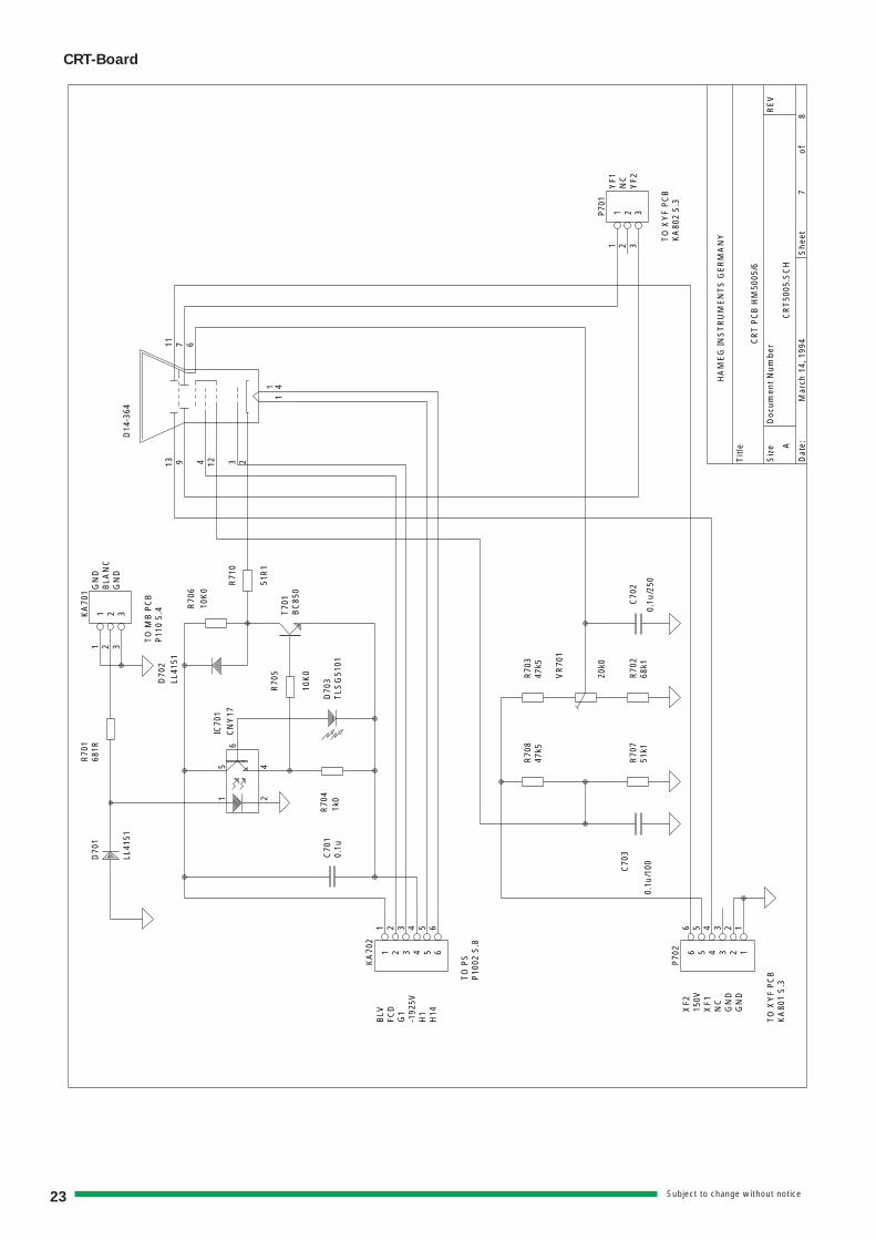
CRT-Board

24Subject to change without notice
Power Supply Board

Subject to change without notice25
RA-Board
26Subject to change without notice
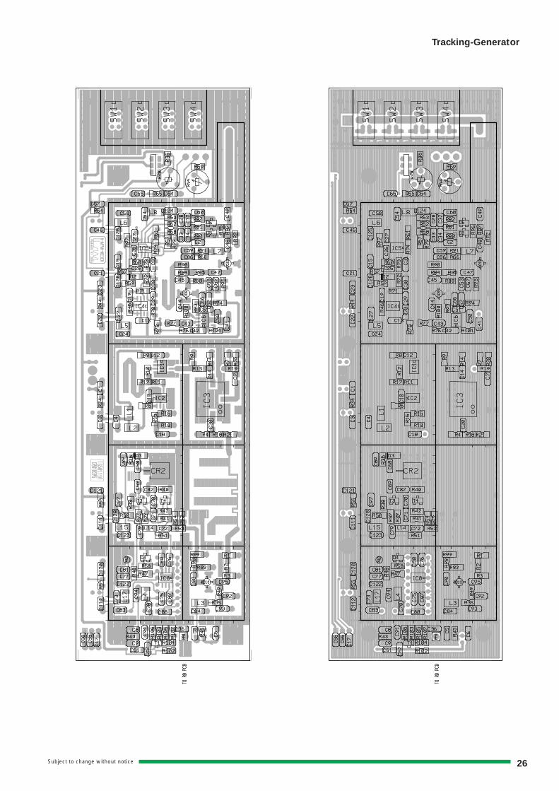
Tracking-Generator

Subject to change without notice27
TO
RB-Board

28Subject to change without notice
Main Board

Subject to change without notice29
Main board

30Subject to change without notice
XY-Board

Subject to change without notice31
XY-Board

32Subject to change without notice
FC-Board

Subject to change without notice33
FC-Board

34Subject to change without notice
PA-Board

Subject to change without notice35
CRT-Board

36Subject to change without notice
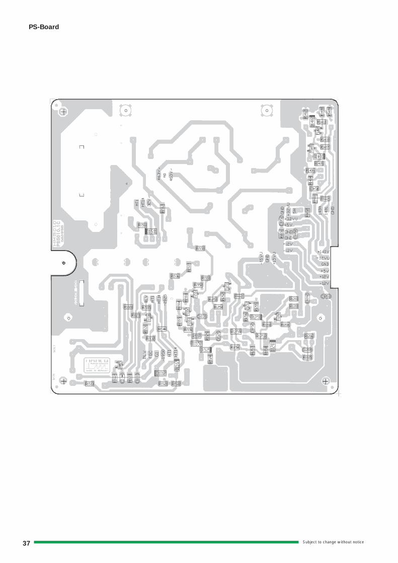
PS-Board
Subject to change without notice37
PS-Board

38Subject to change without notice
PS-Board

Block Diagram HM5010/HM5011
Subject to change without notice39

HAMEG GmbH
Industriestraße 6D-63533 MainhausenTelefon: +49 (0) 6182 / 800-0Telefax: +49 (0) 6182 / 800-100E-mail: [email protected]
Printed in Germany
Oscilloscopes
Multimeters
Counters
Frequency Synthesizers
Generators
R- and LC-Meters
Spectrum Analyzers
Power Supplies
Curve Tracers
Time Standards
Internet:www.hameg.de
4S-5
010-
0010


