6 SUMMER 2021 IEEE SOLID-STATE CIRCUITS MAGAZINE
THE ANALOG MIND
Behzad Razavi
MThe Design of a Low-Voltage Bandgap Reference
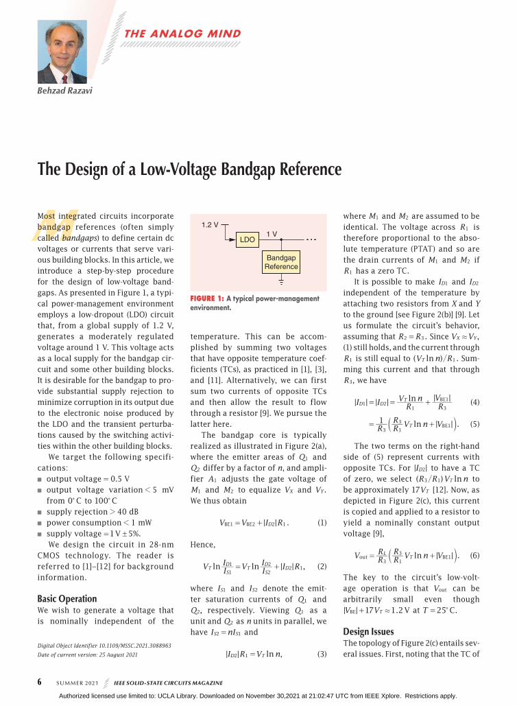
Most integrated circuits incorporate bandgap references (often simply called bandgaps) to define certain dc voltages or currents that serve vari-ous building blocks. In this article, we introduce a step-by-step procedure for the design of low-voltage band-gaps. As presented in Figure 1, a typi-cal power-management environment employs a low-dropout (LDO) circuit that, from a global supply of 1.2 V, generates a moderately regulated voltage around 1 V. This voltage acts as a local supply for the bandgap cir-cuit and some other building blocks. It is desirable for the bandgap to pro-vide substantial supply rejection to minimize corruption in its output due to the electronic noise produced by the LDO and the transient perturba-tions caused by the switching activi-ties within the other building blocks.
We target the following specifi-cations:
output voltage = 0.5 V output voltage variation 1 5 mV
from 0 Cc to 100 Cc supply rejection 2 40 dB power consumption 1 1 mW supply voltage %.1 5V!=
We design the circuit in 28-nm CMOS technology. The reader is referred to [1]–[12] for background information.
Basic OperationWe wish to generate a voltage that is nominally independent of the
temperature. This can be accom-plished by summing two voltages that have opposite temperature coef-ficients (TCs), as practiced in [1], [3], and [11]. Alternatively, we can first sum two currents of opposite TCs and then allow the result to flow through a resistor [9]. We pursue the latter here.
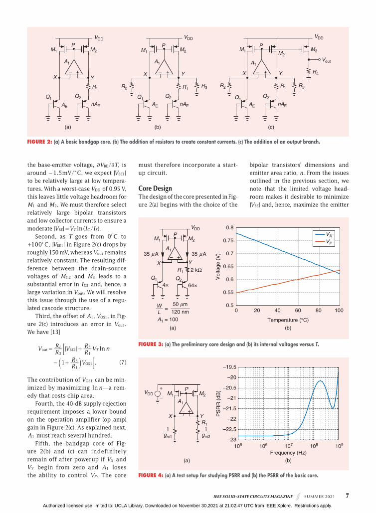
The bandgap core is typically realized as illustrated in Figure 2(a), where the emitter areas of Q1 and Q2 differ by a factor of n, and ampli-fier A1 adjusts the gate voltage of M1 and M2 to equalize VX and .VY We thus obtain
| |V V I RD2 11 2BE BE= + . (1)
Hence,
| | ,ln lnV II V I
I I RTS
DT
S
DD
1
1
2
22 1= + (2)
where IS1 and IS2 denote the emit-ter saturation currents of Q1 and
,Q2 respectively. Viewing Q1 as a unit and Q2 as n units in parallel, we have I nIS S2 1= and
| | ,lnI R V nD T2 1 = (3)
where M1 and M2 are assumed to be identical. The voltage across R1 is therefore proportional to the abso-lute temperature (PTAT) and so are the drain currents of M1 and M2 if R1 has a zero TC.
It is possible to make ID1 and ID2 independent of the temperature by attaching two resistors from X and Y to the ground [see Figure 2(b)] [9]. Let us formulate the circuit’s behavior, assuming that .R R2 3= Since ,V VX Y. (1) still holds, and the current through R1 is still equal to ( ) ./lnV n RT 1 Sum-ming this current and that through
,R3 we have
| | | | | |lnI I RV n
RV
D DT
1 21 3
1BE= = + (4)
| | .lnR RR V n V1
T3 1
31BE= +c m (5)
The two terms on the right-hand side of (5) represent currents with opposite TCs. For | |ID2 to have a TC of zero, we select ( )/ lnR R V nT3 1 to be approximately V17 T [12]. Now, as depicted in Figure 2(c), this current is copied and applied to a resistor to yield a nominally constant output voltage [9],
.| |lnV RR
RR V n VL
T3 1
31out BE= +c m (6)
The key to the circuit’s low-volt-age operation is that Vout can be arbitrarily small even though | | .V V17 1 2VTBE .+ at .T 25 C= c
Design IssuesThe topology of Figure 2(c) entails sev-eral issues. First, noting that the TC of
Digital Object Identifier 10.1109/MSSC.2021.3088963
Date of current version: 25 August 2021
LDO
1.2 V
BandgapReference
1 V
FIGURE 1: A typical power-management environment.
Authorized licensed use limited to: UCLA Library. Downloaded on November 30,2021 at 21:02:47 UTC from IEEE Xplore. Restrictions apply.
IEEE SOLID-STATE CIRCUITS MAGAZINE SUMMER 2021 7
the base-emitter voltage, ,/V TBE2 2 is around . ,V/1 5m C- c we expect | |V 1BE to be relatively large at low tempera-tures. With a worst-case VDD of 0.95 V, this leaves little voltage headroom for M1 and .M2 We must therefore select relatively large bipolar transistors and low collector currents to ensure a moderate | | ( )./lnV V I IT C SBE =
Second, as T goes from 0 Cc to 100 C,+ c | |V 1BE in Figure 2(c) drops by
roughly 150 mV, whereas Vout remains relatively constant. The resulting dif-ference between the drain-source voltages of M ,1 2 and M3 leads to a substantial error in ID3 and, hence, a large variation in .Vout We will resolve this issue through the use of a regu-lated cascode structure.
Third, the offset of ,A1 ,V 1OS in Fig-ure 2(c) introduces an error in .Vout We have [13]
| |
.
lnVRR V
RR V n
RR V1
LT
3 1
3
1
3
out 1
1
BE
OS
= +
- +c m
;
E (7)
The contribution of V 1OS can be min-imized by maximizing lnn—a rem-edy that costs chip area.
Fourth, the 40-dB supply-rejection requirement imposes a lower bound on the operation amplifier (op amp) gain in Figure 2(c). As explained next, A1 must reach several hundred.
Fifth, the bandgap core of Fig-ure 2(b) and (c) can indefinitely remain off after powerup if VX and VY begin from zero and A1 loses the ability to control .VP The core
must therefore incorporate a start-up circuit.
Core DesignThe design of the core presented in Fig-ure 2(a) begins with the choice of the
bipolar transistors’ dimensions and emitter area ratio, n. From the issues outlined in the previous section, we note that the limited voltage head-room makes it desirable to minimize | |VBE and, hence, maximize the emitter
VDD VDD VDD
Vout
M2 M2 M2M3M1 M1 M1
P P P
R1 R1R1R2 R2R3 R3
A1 A1 A1
AE AE AE
RL
nAE nAE nAE
Q2 Q2 Q2Q1 Q1 Q1
YY Y
X X X– –+ + – +
(a) (b) (c)
FIGURE 2: (a) A basic bandgap core. (b) The addition of resistors to create constant currents. (c) The addition of an output branch.
2 kΩ
Temperature (°C)
(b)(a)
0.5
0.55
0.6
0.65
0.7
0.75
0.8
Vol
tage
(V
)
VX
VP
VDD
M2M1P
R1
A1
Q2Q1
YX– +
4× 64×
35 µA35 µA
0 20 40 60 80 100=120 nm
WL
50 µm
A1 = 100
FIGURE 3: (a) The preliminary core design and (b) its internal voltages versus T.
1
105 106 107 108 109
Frequency (Hz)
(b)(a)
–23
–22.5
–22
–21.5
–21
–20.5
–20
–19.5
PS
RR
(dB
)VDD+
+
–
–
M1
R1
M2
A1
P
X Y
gm1
1gm2
FIGURE 4: (a) A test setup for studying PSRR and (b) the PSRR of the basic core.
Authorized licensed use limited to: UCLA Library. Downloaded on November 30,2021 at 21:02:47 UTC from IEEE Xplore. Restrictions apply.
8 SUMMER 2021 IEEE SOLID-STATE CIRCUITS MAGAZINE
areas. But the op amp-offset issue demands that n also be large, leading to an area-hungry solution. As a rea-sonable compromise, we select four unit transistors for Q1, each having
an emitter area of 5 m 5 m,#n n and 64 units for .Q2 Thus, | |V 750 mVBE . and lnV n 72mVT . at room tempera-ture. The weak dependence of lnV nT upon n suggests that the effect of offset in (7) cannot be reduced easily through this variable.
Another approach to lowering the effect of the op amp offset in Fig-ure 2(a) involves scaling ID1 up with respect to .ID2 Denoting this ratio by m, we recognize from (2) that
| | ( ).lnI R V n mD T2 1 $= (8)
This result carries over to (7). Never-theless, an m value substantially grea - ter than unity also raises | |,V 1BE exac-erbating the metal-oxide-semiconduc-tor (MOS) transistor voltage headroom iss- ue at low temperatures. For exam-
ple, if 16,m = | |I RD2 1 is doubled, but | | ( )/ln lnV V mI I V mT D S T1 11BE = = +
( )/lnV I IT D S1 1 also increases by lnV 16 66mVT = at T 0 C.= c We there-
fore maintain 1m = and target a low VOS by proper op amp design.
The next task is to select the bias current in each branch, the value of
,R1 and the dimensions of M1 and .M2 Anticipating about half a dozen
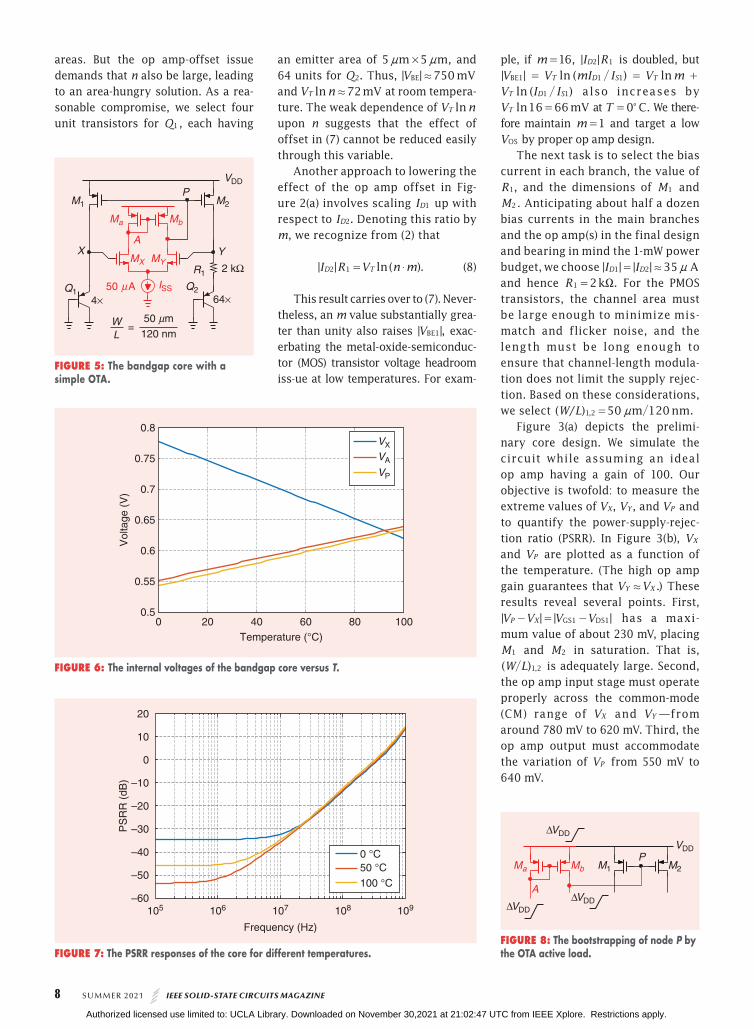
bias currents in the main branches and the op amp(s) in the final design and bearing in mind the 1-mW power budget, we choose | | | |I I 35 AD D1 2 . n= and hence R 2k .1 X= For the PMOS transistors, the channel area must be large enough to minimize mis-match and flicker noise, and the length must be long enough to en sure that channel-length modula-tion does not limit the supply rejec-tion. Based on these considerations, we select ( / ) /W L 50 120m nm.,1 2 n=
Figure 3(a) depicts the prelimi-nary core design. We simulate the circuit while assuming an ideal op amp having a gain of 100. Our objective is twofold: to measure the extreme values of ,VX ,VY and VP and to quantify the power-supply-rejec-tion ratio (PSRR). In Figure 3(b), VX and VP are plotted as a function of the temperature. (The high op amp gain guarantees that .)V VY X. These results reveal several points. First, | | | |V V V VP X 1 1GS DS- = - has a maxi-mum value of about 230 mV, placing M1 and M2 in saturation. That is, ( )/W L ,1 2 is adequately large. Second, the op amp input stage must operate properly across the common-mode (CM) range of VX and VY —from around 780 mV to 620 mV. Third, the op amp output must accommodate the variation of VP from 550 mV to 640 mV.
M1
VDD
M2
MX
Ma Mb
MY
P
Q2Q1
YX
2 kΩR1
4× 64×50 µA
=120 nm
WL
50 µm
ISS
A
FIGURE 5: The bandgap core with a simple OTA.
Temperature (°C)
0.5
0.55
0.6
0.65
0.7
0.75
0.8
Vol
tage
(V
)
VX
VA
VP
0 20 40 60 80 100
FIGURE 6: The internal voltages of the bandgap core versus T.
105 106 107 108 109
Frequency (Hz)
–60
–50
–40
–30
–20
–10
0
10
20
PS
RR
(dB
)
0 °C50 °C
100 °C
FIGURE 7: The PSRR responses of the core for different temperatures.
∆VDD
∆VDD
∆VDD
VDD
Ma M1 M2MbP
A
FIGURE 8: The bootstrapping of node P by the OTA active load.
Authorized licensed use limited to: UCLA Library. Downloaded on November 30,2021 at 21:02:47 UTC from IEEE Xplore. Restrictions apply.
IEEE SOLID-STATE CIRCUITS MAGAZINE SUMMER 2021 9
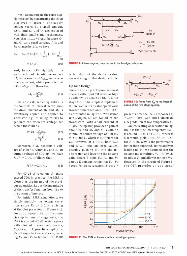
Next, we investigate the core’s sup-ply rejection by constructing the setup displayed in Figure 4. The supply voltage varies by a small amount,
,VDDT and Q1 and Q2 are replaced with their small-signal resistances. Note that / /g g1 1m m1 2= because Q1 and Q2 carry equal currents. If ID1 and ID2 change by ,IDT we have
V V I R g I g1 1
Y X Dm
Dm
12 1
T T T T- = + -c m (9)
,I RD 1T= (10)
and, hence, .V A I RP D1 1T T= In a well-designed circuit, we expect
IDT to be small and V 1,2GS to be rela-tively constant, which predicts that
.V VP DDT T. It follows that
.I A RV
D1 1
DDT T. (11)
We now ask, which quantity is the “output” of interest here? Since the drain current of M1 and M2 is eventually copied and applied to a resistor [e.g., RL in Figure 2(c)] to generate the reference voltage, we define the PSRR as
I RVPSRRD L
DD
TT= (12)
.RA R
L
1 1. (13)
Moreover, if R1 sustains a volt-age of lnV n 72mVT . mV and RL an output voltage of 500 mV, we have
. ./R R 0 14L1 = It follows that
. .A0 14PSRR 1= (14)
For 40 dB of rejection, A1 must exceed 700. In practice, the PSRR is plotted as the inverse of the previ-ous quantities, i.e., as the magnitude of the transfer function from VDD to the output of interest.
For initial PSRR simulations, we simply multiply the voltage varia-tion across R1 by . ,/1 0 14 arriving at the plot presented in Figure 4(b). For supply-perturbation frequen-cies up to tens of megahertz, the PSRR is around –23 dB, which agrees with (14). At higher frequencies, C C1 2GS GS+ in Figure 4(a) couples the VDD changes to C 1GD and ,C 2GD caus-ing VX and VY to bounce. The PSRR
is far short of the desired value, necessitating further design efforts.
Op Amp DesignSince the op amp in Figure 3(a) must operate with input CM levels as high as 780 mV, we select an NMOS input stage for it. The simplest implemen-tation is a five-transistor operational transconductance amplifier (OTA), as presented in Figure 5. We assume / /W L 50 120m nmn= for all of the
transistors. With a tail current of 50 μA, the op amp provides a gain of about 20, and MX and MY exhibit a minimum source voltage of 350 mV at ,T 100 C= c which is sufficient for
.ISS However, at ,T 0 C= c both | |VBE and | |V 1,2TH take on large values, possibly pushing MX into the tri-ode region and lowering the op amp gain. Figure 6 plots ,VX ,VA and VP versus T, demonstrating that V VX A- keeps MX in saturation. Figure 7
presents how the PSRR responses at ,T 0 C= c 50 Cc , and 010 Cc illustrate
a degradation at low temperatures.An interesting observation in Fig-
ure 7 is that the low-frequency PSRR is around –35 dB at ,T 0 C= c whereas (14) would yield ( . )/ A1 0 14 9dB1 / - for .A 201 = Why is the performance better than expected? In the analysis leading to (14), we assumed that the op amp must multiply V VY X- by A1 to adjust VP and allow it to track .VDD However, in the circuit of Figure 5, the OTA provides an additional
Mc Ma MbMd
VDD
Ra
MX MY
Rb
YX
ToNode P
50 µA ISS
Ra = Rb = 40 kΩ
=120 nm
WL
50 µm
FIGURE 9: A two-stage op amp for use in the bandgap reference.
Mc Ma MbMd
VDD
∆VDD
∆VDD ∆VDD
FIGURE 10: Paths from VDD to the internal nodes of the two-stage op amp.
105 106 107 108 109
Frequency (Hz)
–60
–50
–40
–30
–20
–10
0
10
20
PS
RR
(dB
)
0 °C50 °C
100 °C
FIGURE 11: The PSRR of the core with a two-stage op amp.
Authorized licensed use limited to: UCLA Library. Downloaded on November 30,2021 at 21:02:47 UTC from IEEE Xplore. Restrictions apply.
10 SUMMER 2021 IEEE SOLID-STATE CIRCUITS MAGAZINE
tracking mechanism: If VDD varies by ,VDDT so do VA and VP (Figure 8). In essence, the OTA’s PMOS active load bootstraps P to .VDD
That V VP AT T. can be seen by noting that, in the absence of asym-metries within the op amp, V VP A= if .V VX Y= This property is generally considered a drawback of the five-transistor OTA, but it proves useful here. Since the VDD perturbation is directly applied to node P by Ma and
,Mb the op amp provides only addi-tional correction.
The PSRR degradation at low tem-peratures calls for a higher op amp gain and, hence, a two-stage topol-ogy. Figure 9 illustrates a simple design wherein the output CM level of the first stage is set by Ra and Rb to be equal to one PMOS source-gate voltage below .VDD This method also defines the bias currents of the sec-ond stage by forming current mir-rors. Thus, the total supply current is about 100 μA. This op amp offers a gain of 380 at T 0 C= c and 320 at ,T 100 C= c improving the PSRR according to (14).
Does the effect illustrated in Fig-ure 8 exist in the two-stage op amp as well? If V VX Y. and VDD changes by
,VDDT then so do the drain voltages of Ma and Mb (Figure 10). We observe that the gate-source voltages of Mc and Md remain relatively constant, introducing little change at their drains and, hence, in .VP In other
Temperature (°C)(b)(a)
93.25
93.3
93.35
93.4
93.45
93.5
93.55
93.6
93.65
|I D2|(
uA)
2 kΩ
VDD
M3M2M1
P
R1R2 R3
A1
Q2Q1
YX – +
4× 64×
35 µA
13 kΩ
5.5 kΩ
13 kΩ
35 µA
50 µm=
120 nmWL
Vout
RL
0 20 40 60 80 100
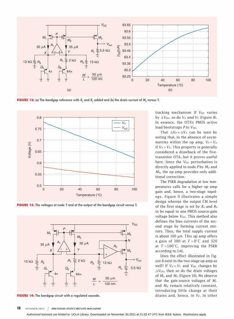
FIGURE 12: (a) The bandgap reference with R2 and R3 added and (b) the drain current of M2 versus T.
Temperature (°C)
0.5
0.55
0.6
0.65
0.7
0.75
0.8
Vol
tage
(V
)
VY
Vout
0 20 40 60 80 100
FIGURE 13: The voltages at node Y and at the output of the bandgap circuit versus T.
2 kΩ
VDD
M3
M4
M2
M1
P
R1R2 R3
A1A2
Q2Q1
YX – –+
+
4× 64×
35 µA
13 kΩ5.5 kΩ
13 kΩ
35 µA
50 µm=
120 nmW
L
Vout
RL
N
FIGURE 14: The bandgap circuit with a regulated cascode.
Authorized licensed use limited to: UCLA Library. Downloaded on November 30,2021 at 21:02:47 UTC from IEEE Xplore. Restrictions apply.
IEEE SOLID-STATE CIRCUITS MAGAZINE SUMMER 2021 11
words, this op amp does not provide the direct cancelation mechanism of the five-transistor OTA. Figure 11 plots the bandgap core PSRR in the presence of the two-stage op amp.
Complete Bandgap ReferenceAs prescribed by Figure 2(b), we must attach equal resistors from nodes X and Y to the ground to change the nature of ID1 and ID2 from PTAT to temperature-independent quantities. This requires that ( )/ lnR R V nT3 1 be around V17 T and R R R62 3 1.= if
.n 16= Figure 12 displays the modi-fied circuit as well as | |ID2 versus T. Resistors R2 and R3 are rounded up to ,13kX and the op amp is imple-mented as the two-stage topology of Figure 9. We note that | |ID2 changes by less than 0.4% across our temper-ature range of interest.
In the next step, we copy ID2 and apply the result to ,RL forming the ref-erence voltage, .Vout According to (6), an output voltage of 0.5 V requires
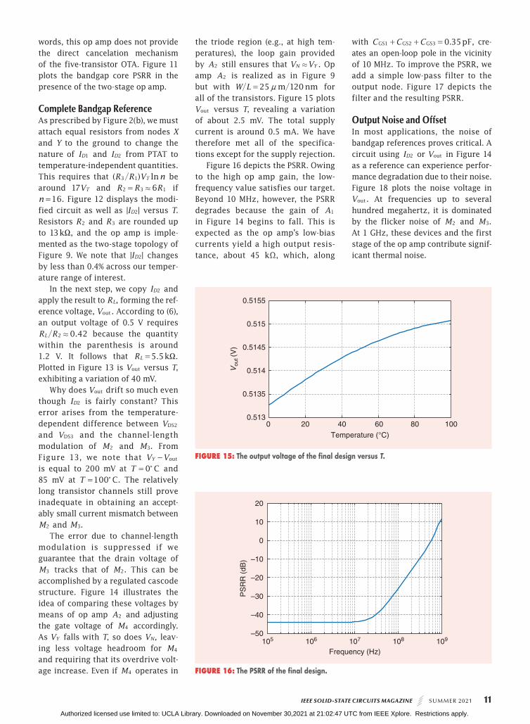
./R R 0 42L 2 . because the quantity within the parenthesis is around 1.2 V. It follows that . .R 5 5kL X= Plotted in Figure 13 is Vout versus T, exhibiting a variation of 40 mV.
Why does Vout drift so much even though ID2 is fairly constant? This error arises from the temperature-dependent difference between V 2DS and V 3DS and the channel-length modulation of M2 and .M3 From Figure 13, we note that V VY out- is equal to 200 mV at T 0 C= c and 85 mV at .T 100 C= c The relatively long transistor channels still prove inadequate in obtaining an accept-ably small current mismatch between M2 and .M3
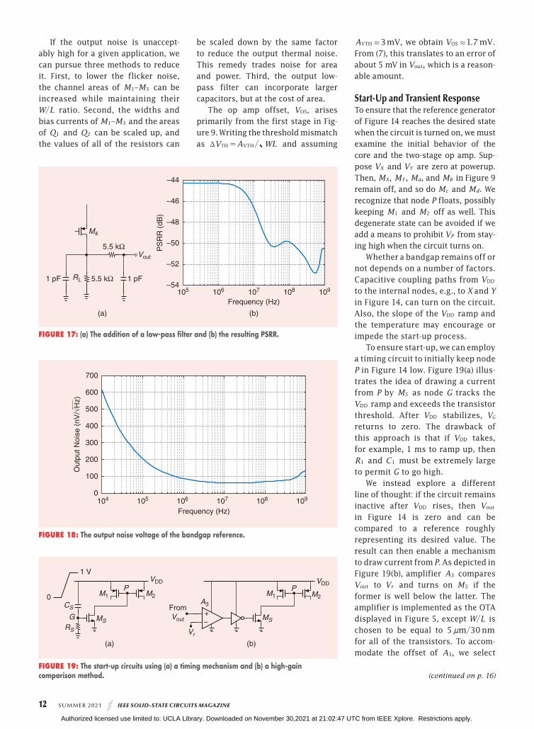
The error due to channel-length modulation is suppressed if we guarantee that the drain voltage of M3 tracks that of .M2 This can be accomplished by a regulated cascode structure. Figure 14 illustrates the idea of comparing these voltages by means of op amp A2 and adjusting the gate voltage of M4 accordingly. As VY falls with T, so does ,VN leav-ing less voltage headroom for M4 and requiring that its overdrive volt-age increase. Even if M4 operates in
the triode region (e.g., at high tem-peratures), the loop gain provided by A2 still ensures that .V VN Y. Op amp A2 is realized as in Figure 9 but with / /W L 25 0m 12 nmn= for all of the transistors. Figure 15 plots Vout versus T, revealing a variation of about 2.5 mV. The total supply current is around 0.5 mA. We have therefore met all of the specifica-tions except for the supply rejection.
Figure 16 depicts the PSRR. Owing to the high op amp gain, the low-frequency value satisfies our target. Beyond 10 MHz, however, the PSRR degrades because the gain of A1 in Figure 14 begins to fall. This is expected as the op amp’s low-bias currents yield a high output resis-tance, about 45 kΩ, which, along
with .C C C 0 35pF,1 2 3GS GS GS+ + = cre-ates an open-loop pole in the vicinity of 10 MHz. To improve the PSRR, we add a simple low-pass filter to the output node. Figure 17 depicts the filter and the resulting PSRR.
Output Noise and OffsetIn most applications, the noise of bandgap references proves critical. A circuit using ID2 or Vout in Figure 14 as a reference can experience perfor-mance degradation due to their noise. Figure 18 plots the noise voltage in
.Vout At frequencies up to several hundred megahertz, it is dominated by the flicker noise of M2 and .M3 At 1 GHz, these devices and the first stage of the op amp contribute signif-icant thermal noise.
Temperature (°C)
0 20 40 60 80 1000.513
0.5135
0.514
0.5145
0.515
0.5155
Vou
t (V
)
FIGURE 15: The output voltage of the final design versus T.
105 106 107 108 109
Frequency (Hz)
–50
–40
–30
–20
–10
0
10
20
PS
RR
(dB
)
FIGURE 16: The PSRR of the final design.
Authorized licensed use limited to: UCLA Library. Downloaded on November 30,2021 at 21:02:47 UTC from IEEE Xplore. Restrictions apply.
12 SUMMER 2021 IEEE SOLID-STATE CIRCUITS MAGAZINE
If the output noise is unaccept-ably high for a given application, we can pursue three methods to reduce it. First, to lower the flicker noise, the channel areas of M1–M3 can be increased while maintaining their /W L ratio. Second, the widths and
bias currents of M1–M3 and the areas of Q1 and Q2 can be scaled up, and the values of all of the resistors can
be scaled down by the same factor to reduce the output thermal noise. This remedy trades noise for area and power. Third, the output low-pass filter can incorporate larger capacitors, but at the cost of area.
The op amp offset, ,VOS arises primarily from the first stage in Fig-ure 9. Writing the threshold mismatch as /V A WLTH VTHT = and assuming
A 3mV,VTH . we obtain .V 1 7 mV.OS . From (7), this translates to an error of about 5 mV in ,Vout which is a reason-able amount.
Start-Up and Transient ResponseTo ensure that the reference generator of Figure 14 reaches the desired state when the circuit is turned on, we must examine the initial behavior of the core and the two-stage op amp. Sup-pose VX and VY are zero at powerup. Then, ,MX ,MY ,Ma and Mb in Figure 9 remain off, and so do Mc and .Md We recognize that node P floats, possibly keeping M1 and M2 off as well. This degenerate state can be avoided if we add a means to prohibit VP from stay-ing high when the circuit turns on.
Whether a bandgap remains off or not depends on a number of factors. Capacitive coupling paths from VDD to the internal nodes, e.g., to X and Y in Figure 14, can turn on the circuit. Also, the slope of the VDD ramp and the temperature may encourage or impede the start-up process.
To ensure start-up, we can employ a timing circuit to initially keep node P in Figure 14 low. Figure 19(a) illus-trates the idea of drawing a current from P by MS as node G tracks the VDD ramp and exceeds the transistor threshold. After VDD stabilizes, VG returns to zero. The drawback of this approach is that if VDD takes, for example, 1 ms to ramp up, then R1 and C1 must be extremely large to permit G to go high.
We instead explore a different line of thought: if the circuit remains inactive after VDD rises, then Vout in Figure 14 is zero and can be compared to a reference roughly representing its desired value. The result can then enable a mechanism to draw current from P. As depicted in Figure 19(b), amplifier A3 compares Vout to Vr and turns on MS if the former is well below the latter. The amplifier is implemented as the OTA displayed in Figure 5, except /W L is chosen to be equal to /5 30m nmn for all of the transistors. To accom-modate the offset of ,A3 we select
104 105 106 107 108 109
Frequency (Hz)
0
100
200
300
400
500
600
700
Out
put N
oise
(nV
/√H
z)
FIGURE 18: The output noise voltage of the bandgap reference.
VDD VDDP P
1 V
0CS
RS
A3
Vr
MS MSG
M2 M2M1 M1
FromVout
+–
(b)(a)
FIGURE 19: The start-up circuits using (a) a timing mechanism and (b) a high-gain comparison method. (continued on p. 16)
5.5 kΩ
5.5 kΩ
1 pF 1 pF
105 106 107 108 109
Frequency (Hz)
(b)(a)
–54
–52
–50
–48
–46
–44
PS
RR
(dB
)
RL
Vout
M4
FIGURE 17: (a) The addition of a low-pass filter and (b) the resulting PSRR.
Authorized licensed use limited to: UCLA Library. Downloaded on November 30,2021 at 21:02:47 UTC from IEEE Xplore. Restrictions apply.
16 SUMMER 2021 IEEE SOLID-STATE CIRCUITS MAGAZINE
of ac coupling attenuates the low-fre-quency component of the signal, caus-ing baseline wander, which may result in the loss of data in wireline communica-tion. To restore this low-frequency com-ponent for a random binary sequence or, equivalently, to remove the base -line wander, we employ a comparator with quantized feedback in conjunction with superposition.
AcknowledgmentI would like to thank Hossein Shakiba (the author of [2]) for his insights and discussions that inspired this article.
References[1] B . E . Boser, “Of fset control ,” in EECS
247: Lecture Notes 27, Berkeley, CA: Univ. of California, 2002, pp. 1–15. [Online]. Available: https://inst.eecs .berkeley.edu//~n247/fa07/lectures/L27 .pdf
[2] M. H. Shakiba, “A 2.5Gb/s adaptive cable equalizer,” in Proc. Dig. Tech. IEEE Int. Solid-State Circuits Conf. (ISSCC), Feb. 1999, pp. 396–397. doi: 10.1109/ISSCC .1999.759317.
[3] F. Waldhauer “Quantized feedback in an experimental 280-Mb/s digital repeater for coaxial transmission,” IEEE Trans. Commun., vol. 22, no. 1, pp. 1–5, Jan. 1974. doi: 10.1109/TCOM.1974.1092055.
[4] A. Sheikholeslami, “Circuit intuitions: Equalizer circuit,” IEEE Solid State Circuits Mag., vol. 12, no. 1, pp. 6–7, Winter 2020. doi: 10.1109/MSSC.2019.2952233.
THE ANALOG MIND (continued from p. 12)
.V 0 4 Vr . and generate it from VDD by a resistive divider. Figure 20(a) and (b) plots ,VDD ,VP and Vout for a 900-ns VDD ramp before and after the start-up circuit is added, respec-tively. We note that the former fails (in fact, it oscillates with a period of several microseconds) whereas the latter settles properly. For a 1-ms VDD ramp, the bandgap turns on with or without the start-up mechanism.
References[1] R. J. Widlar, “Some circuit design tech-
niques for linear integrated circuits,” IEEE Trans. Circuit Theory, vol. 12, no. 4, pp. 586–590, Dec. 1965. doi: 10.1109/TCT .1965.1082512.
[2] R. J. Widlar, “New developments in IC voltage regulators,” IEEE J. Solid-State Cir-cuits, vol. 6, no. 1, pp. 2–7, Feb. 1971. doi: 10.1109/JSSC.1971.1050151.
[3] A. P. Brokaw, “A simple three-terminal IC bandgap reference,” IEEE J. Solid-State Cir-cuits, vol. 9, no. 6, pp. 388–393, Dec. 1974. doi: 10.1109/JSSC.1974.1050532.
[4] R. A. Blauschild, P. A. Tucci, R. S. Muller, and R. G. Meyer, “A new NMOS temperature-
stable voltage reference,” IEEE J. Solid-State Circuits, vol. 13, no. 6, pp. 767–774, Dec. 1978. doi: 10.1109/JSSC.1978.1052048.
[5] Y. P. Tsividis and R. W. Ulmer, “A CMOS volt-age reference,” IEEE J. Solid-State Circuits, vol. 13, no. 6, pp. 774–778, Dec. 1978. doi: 10.1109/JSSC.1978.1052049.
[6] E. A. Vittoz and O. Neyroud, “A low-voltage CMOS bandgap reference,” IEEE J. Solid-State Circuits, vol. 14, no. 3, pp. 573–577, June 1979. doi: 10.1109/JSSC.1979.1051218.
[7] R. Gregorian, G. Wegner, and W. E. Nich-olson, “An integrated single-chip PCM voice codec with filters,” IEEE J. Solid-State Circuits, vol. 16, no. 4, pp. 322–333, Aug. 1981. doi: 10.1109/JSSC.1981. 1051596.
[8] K. E. Kujik, “A precision reference voltage source,” IEEE J. Solid-State Circuits, vol. 8, pp. 222–226, June 1973. doi: 10.1109/JSSC .1973.1050378.
[9] H. Banba et al., “A CMOS bandgap reference circuit with Sub-1-V operation,” IEEE J. Sol-id-State Circuits, vol. 34, no. 5, pp. 670–674, May 1999. doi: 10.1109/4.760378.
[10] C. J. B. Fayomi et al., “Sub-1-V CMOS band-gap reference design techniques: A sur-vey,” Analog Integr. Circuits Signal Pro-cess., vol. 62, no. 2, pp. 141–157, Feb. 2010. doi: 10.1007/s10470-009-9352-4.
[11] H. Neuteboom, B. M. J. Kup, and M. Jans-sens, “A DSP-based hearing instrument IC,” IEEE J. Solid-State Circuits, vol. 32, no. 11, pp. 1790–1806, Nov. 1997. doi: 10.1109/ 4.641702.
[12] B. Razavi, “The bandgap reference,” IEEE Sol-id State Circuits Mag., vol. 8, no. 3, pp. 9–12, Summer 2016. doi: 10.1109/MSSC.2016 .2577978.
[13] B. Razavi, Design of Analog CMOS Integrat-ed Circuits, 2nd ed., New York, NY, USA: McGraw-Hill, 2017.
Time (ns)
0
0.2
0.4
0.6
0.8
1
Vol
tage
(V
)
0
0.2
0.4
0.6
0.8
1
Vol
tage
(V
)
VDD VP Vout
Time (ns)(a) (b)
0 200 400 600 800 1,000 0 200 400 600 800 1,000
FIGURE 20: The bandgap internal waveforms (a) without and (b) with the start-up circuit.
Authorized licensed use limited to: UCLA Library. Downloaded on November 30,2021 at 21:02:47 UTC from IEEE Xplore. Restrictions apply.


