
CMxxxwww.custom.it
Thermal printing mechanismCMxxx
User’s Manual

CMxxx
All rights reserved. Total or even partial reproduction of this manual in anyform, whether on paper or electronically, is strictly forbidden. While CUSTOMENGINEERING SPA guarantees that the information contained in this manualhas been carefully checked and verified, CUSTOM ENGINEERING SPA andother resources utilized in its creation assume no responsibility for situationsarising from its use.Feedback regarding any errors in the manual’s content or suggestions onhow it could be improved would be greatly appreciated. Since its productsare subject to continuous checking and improvement, CUSTOMENGINEERING SPA reserves the right to modify the information containedin this manual without prior notice.
COD. DOME - CMxxx VERS. PRELIMINARY
Copyright 2001 CUSTOM ENGINEERING SPA – Italy
CUSTOM ENGINEERING SPAStr. Berettine 2 - 43010 Fontevivo (PARMA) - ItalyTel. : +39 0521-680111 - Fax : +39 0521-610701http: www.custom.it http: www.smice.com
To contact our Technical Support :Phone. : +39 0521-680163 - Fax : +39 0521-680146Email : [email protected]

CMxxx
2
3A
4
B
1
B
A
CA
Printing mechanism models
A. Front exterior view CMxxx (1)
1- Motor2- Head Set3- Print Head4- Head leverA- Paper outfeedB- Paper inputC- Sensor Head up detection
(1) The XXX suffix indicates the following models :CM58CM60CM60A (2)
CM80CM112CM112A (2)
CM210CM210A (2)
CM216CM216A (2)
(2) The versions CM60A, CM112A, CM210Aand CM216A are complete with auto-cutter.
CM60 left side view

CMxxx
4
3 B 3
1
2 C
B
A
A
CM60A left side view
B. Front exterior view CM60A
1- Motor2- Head Set3- Cutter4- Head leverA- Paper outfeedB- Paper inputC- Sensor Head up detection
CM60A top view
TABLE OF CONTENTS
CMxxxi
INTRODUCTION
CONVENTIONS USED IN THE MANUAL ..................................................... 1GENERAL SPECIFICATIONS ...................................................................... 2DESCRIPTION OF THE MECHANISM ......................................................... 3MAIN FEATURES........................................................................................... 3
1. CONNECTIONS
1.1 ELECTRIC CIRCUIT BLOCK DIAGRAM OF CM58 MODEL ............ 1-11.2 ELECTRIC CIRCUIT BLOCK DIAGRAM OF CM60 MODEL ............ 1-21.3 ELECTRIC CIRCUIT BLOCK DIAGRAM OF CM80 MODEL ............ 1-31.4 ELECTRIC CIRCUIT BLOCK DIAGRAM OF CM112 MODEL .......... 1-41.5 ELECTRIC CIRCUIT BLOCK DIAGRAM OF CM210 MODEL .......... 1-51.6 ELECTRIC CIRCUIT BLOCK DIAGRAM OF CM216 MODEL .......... 1-61.7 ELECTRIC CIRCUIT BLOCK DIAGRAM OF MOTOR....................... 1-71.8 ELECTRIC CIRCUIT BLOCK DIAGRAM OF PAPER SENSOR ....... 1-71.9 ELECTRIC CIRCUIT BLOCK DIAGRAM OF HEAD UP SENSOR.... 1-8
2. PRINT HEAD
2.1 PRINT HEAD ........................................................................................ 2-12.2 OPERATION PRECAUTIONS............................................................. 2-22.3 ELECTRICAL CHARACTERISTICS OF CMXXX SERIES CIRCUIT 2-2
2.3.1 CM58 Table .................................................................................... 2-22.3.2 CM60/CM60A Table ...................................................................... 2-32.3.3 CM80 Table .................................................................................... 2-32.3.4 CM112 Table .................................................................................. 2-42.3.5 CM210/CM210A/CM216/CM216A Table ...................................... 2-4
2.4 SWITCHING CHARCTERISTICS OF CIRCUIT................................. 2-52.5 TIMING CHART OF CM58, CM60, CM80, CM112, CM210 AND CM216
................................................................................................................. 2-52.6 THERMISTOR...................................................................................... 2-6
2.6.1 Thermistor curve ............................................................................ 2-7
TABLE OF CONTENTS
CMxxx ii
3. STEPPER MOTOR
3.1 STEPPER MOTOR .............................................................................. 3-13.1.1 Dynamic torque characteristics ...................................................... 3-2
3.2 PRECAUTION ...................................................................................... 3-2
4. SENSOR
4.1 SENSOR............................................................................................... 4-14.2 GRAPHICS OF TYPICAL CHARACTERISTICS................................ 4-2
5. DIMENSIONS
5.1 DIMENSIONS ....................................................................................... 5-1

INTRODUCTION
CMxxx1
CONVENTIONS USED IN THE MANUAL
N.B.Gives important information or suggestions relative to the use of theprinter
WARNINGThe information marked with this symbol must be carefully heededto safeguard against damaging the printer
DANGER The information marked with this symbol must be carefully heeded to safeguard against injury to the operator.

INTRODUCTION
CMxxx 2
MECHANISM GENERAL SPECIFICATIONS
metI metI metI metI metI noitacificepS noitacificepS noitacificepS noitacificepS noitacificepS
85MC 85MC 85MC 85MC 85MC 06MC 06MC 06MC 06MC 06MC 08MC 08MC 08MC 08MC 08MC 211MC 211MC 211MC 211MC 211MC 012MC 012MC 012MC 012MC 012MC 612MC 612MC 612MC 612MC 612MC
dohtemgnitnirP dohtemtodenillamrehT
htdiwgnitnirpevitceffE mm84 mm65 mm27 mm401 mm612 mm612
)enil/stod(noitarugifnocdaeH 483 844 675 238 8271 8271
hctiPtoD lacitrevmm521.0latnozirohmm521.0
rewopees(deepSgnitnirP)stodrofygrenednanoitpmusnoc
051 s/mm 57 s/mm
)mm(htdiwrepaP 5,0±85 5,0±06 5,0±08 5,0±211 5,0±012 5,0±612
dohtemdeefrepaP,seslup1/eniltod1,deefnoitcirF
noitaticxeesahp2-2ralopib
tod1,deefnoitcirF2-2ralopib,seslup2/enil
noitaticxeesahp
rosneserutarepmetdaeH rotsimrehT
noitcetedrepaP rosnesotohpepytevitcelfeR
stodforebmunmumixaMemitatadetavitca
821 291 291 652 844 844
)vaR(ecnatsisertoD 007 Ω %3±
sebortsforebmuN 3 4
C°5
C°52ygreneredaeH
C°04
)sm22,0(tod/Jm561,0
)sm02,0(tod/Jm51,0
)sm91,0(tod/Jm41,0
)ciR(ecnatsiserdetarutasrevirD 32 Ω
snoisnemidlanretxE)HxDxW(
x6,6019,04x2,06
x6,8019,04x2,06
x6,8219,04x2,06
x6,0619,04x2,06
x6,4829,04x2,06
x6,4829,04x2,06
thgieW .rg262 .rg462 .rg492 .rg043 .rg265 .rg265
cigolegnaregatloVnoitarepO %01±V5
daeheniltodegatloVnoitarepO 8,22 ÷ V2,52
noitpmusnoctnerruC stod/Am13
ytilibaeR/efiL mK05
repapdednammoceR tnelaviuqero05FKnaznaK
(Tab. 1)
INTRODUCTION
CMxxx3
Maximum ratings
retemaraP retemaraP retemaraP retemaraP retemaraP noitacificepS noitacificepS noitacificepS noitacificepS noitacificepS85MC 85MC 85MC 85MC 85MC 06MC 06MC 06MC 06MC 06MC 08MC 08MC 08MC 08MC 08MC 211MC 211MC 211MC 211MC 211MC 012MC 012MC 012MC 012MC 012MC 612MC 612MC 612MC 612MC 612MC
noitpmusnocygreneretaeH)enil/sm5,2eton(tod/Jm72,0)enil/sm52,1eton(tod/Jm81,0)enil/sm526,0eton(tod/Jm51,0
egatlovdaeH )srotcennocneewtebeton(V2,52
egatlovcigoL V52,0±V5+=ddV
gnitarepotnemnorivnEegnarerutarepmet
0 ÷ C°05
ytidimuhgnitarepO 01 ÷ noitasnednoconHR%09
latnemnorivneegarotS 04- ÷ 01ytidimuHC°08 ÷ dedulcxerepaP,noitasnednocon%09
erutarepmetgnitarepomumixaM C°56deecxetonllahsrotsimrehtfoerutarepmetdetceteD
DESCRIPTION OF THE MECHANISM
The main characteristics of the series CM thermal printing mechanism aredefinitely the reliability, the quality and the long lasting performance, making itthe suitable product for industrial environments such as weighting, control,safety systems, as well as medical and portable applications.The sturdy aluminium alloy casing for a higher thermal efficiency and a muchbetter rigidity of the structure.The series CM mechanisms prints at a high 203 dpi resolution on paperweights between 58 and 80 gr/m2 (also labels).The mechanism is featured with a high torque paper-pulling motor, and with asilicon rubber roll.
(Tab. 2)
INTRODUCTION
CMxxx 4
SERIES CMxxx MAIN FEATURES
• Printing width from 58 to 216 mm• High speed 75 ÷ 150 mm/sec• Logic voltage 24V• High resolution 8 dots/mm 203 dpi• Sensors: Paper detection photosensor, paper end sensor
head up detection, temperature sensor thermistor 30K• Life 50 Km Printed paper or 100 millions of pulses• Front or rear paper inlet• CM216 can print into US A4 letter format (216mm paper width)• CM210 and CM216 can print both A5 and A4 format• The models of series CM availables are : CM58, CM60, CM60A, CM80,
CM112, CM112A, CM210, CM210A, CM216 and CM216A• The versions CM60A, CM112A, CM210A and CM216A are complete
with auto-cutter.

1. CONNECTIONS
CMxxx1-1
1, 2, 3
4, 5, 6
11
10
9
14
15
13
VH (+24V)
GND
7VDD (+5V)
STB3
STB2
STB1
LATCH LATCH REGISTER
384 B IT SHIFT REGISTERDATA IN
15 PIN
THERMISTOR 30K B:3950Ω
8TM
128 1129257384 256
CLOCK
(Fig.1.1)
(Tab.1.1)Pin assignments
.oN .oN .oN .oN .oN langiS langiS langiS langiS langiS noitcnuF noitcnuF noitcnuF noitcnuF noitcnuF
11111 HV YLPPUSREWOPDAEH
22222 HV YLPPUSREWOPDAEH
33333 HV YLPPUSREWOPDAEH
44444 DNG DNUORG
55555 DNG DNUORG
66666 DNG DNUORG
77777 DDV YLPPUSREWOPCIGOL
88888 MT ROTSIMREHT
99999 1BTS LANGIS1EBORTS
0101010101 2BTS LANGIS2EBORTS
1111111111 3BTS LANGIS3EBORTS
2121212121 .C.N DETCENNOCTON
3131313131 KCOLC KCOLCLAIRES
4141414141 HCTAL HCTAL
5151515151 NIATAD TUPNIATAD
1.1 ELECTRICAL CIRCUIT BLOCK DIAGRAM OF CM58 MODEL

1. CONNECTIONS
CMxxx 1-2
1, 2, 3
4, 5, 6
11
10
9
14
15
13
VH (+24V)
GND
7VDD (+5V)
STB3
STB2
STB1
LATCH LATCH REGISTER
448 BIT SHIFT REGISTERDATA IN
15 PIN
THERMISTOR 30K B:3950Ω
8TM
128 1129321448 320
CLOCK
Pin assignments
1.2 ELECTRICAL CIRCUIT BLOCK DIAGRAM OF CM60 MODEL
.oN .oN .oN .oN .oN langiS langiS langiS langiS langiS noitcnuF noitcnuF noitcnuF noitcnuF noitcnuF
11111 HV YLPPUSREWOPDAEH
22222 HV YLPPUSREWOPDAEH
33333 HV YLPPUSREWOPDAEH
44444 DNG DNUORG
55555 DNG DNUORG
66666 DNG DNUORG
77777 DDV YLPPUSREWOPCIGOL
88888 MT ROTSIMREHT
99999 1BTS LANGIS1EBORTS
0101010101 2BTS LANGIS2EBORTS
1111111111 3BTS LANGIS3EBORTS
2121212121 .C.N DETCENNOCTON
3131313131 KCOLC KCOLCLAIRES
4141414141 HCTAL HCTAL
5151515151 NIATAD TUPNIATAD
(Tab.1.2)
(Fig.1.2)

1. CONNECTIONS
CMxxx1-3
1, 2, 3
4, 5, 6
11
10
9
14
15
13
VH (+24V)
G N D
7VDD (+5V)
STB3
STB2
STB1
LATCH LATCH REGISTER
576 BIT SHIFT REGISTERDATA IN
15 P IN
TH ER M ISTOR 30K B:3950Ω
8TM
192 1193385576 384
C LO CK
Pin assignments (Tab.1.3)
1.3 ELECTRICAL CIRCUIT BLOCK DIAGRAM OF CM80 MODEL
(Fig.1.3)
.oN .oN .oN .oN .oN langiS langiS langiS langiS langiS noitcnuF noitcnuF noitcnuF noitcnuF noitcnuF
11111 HV YLPPUSREWOPDAEH
22222 HV YLPPUSREWOPDAEH
33333 HV YLPPUSREWOPDAEH
44444 DNG DNUORG
55555 DNG DNUORG
66666 DNG DNUORG
77777 DDV YLPPUSREWOPCIGOL
88888 MT ROTSIMREHT
99999 1BTS LANGIS1EBORTS
0101010101 2BTS LANGIS2EBORTS
1111111111 3BTS LANGIS3EBORTS
2121212121 .C.N DETCENNOCTON
3131313131 KCOLC KCOLCLAIRES
4141414141 HCTAL HCTAL
5151515151 NIATAD TUPNIATAD
1. CONNECTIONS
CMxxx 1-4
1, 2, 3
4, 5, 6
12
10
9
14
15
13
VH (+24V)
GND
7VDD (+5V)
STB4
STB2
STB1
LATCH LATCH REG ISTER
832 BIT SHIFT REGISTERDATA IN
15 PIN
THERM ISTO R 30K B :3950Ω
8TM
CLOCK
192 1193385 384832
STB3
640641
11
Pin assignments
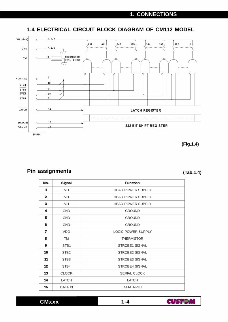
1.4 ELECTRICAL CIRCUIT BLOCK DIAGRAM OF CM112 MODEL
.oN .oN .oN .oN .oN langiS langiS langiS langiS langiS noitcnuF noitcnuF noitcnuF noitcnuF noitcnuF
11111 HV YLPPUSREWOPDAEH
22222 HV YLPPUSREWOPDAEH
33333 HV YLPPUSREWOPDAEH
44444 DNG DNUORG
55555 DNG DNUORG
66666 DNG DNUORG
77777 DDV YLPPUSREWOPCIGOL
88888 MT ROTSIMREHT
99999 1BTS LANGIS1EBORTS
0101010101 2BTS LANGIS2EBORTS
1111111111 3BTS LANGIS3EBORTS
2121212121 4BTS LANGIS4EBORTS
3131313131 KCOLC KCOLCLAIRES
4141414141 HCTAL HCTAL
5151515151 NIATAD TUPNIATAD
(Tab.1.4)
(Fig.1.4)

1. CONNECTIONS
CMxxx1-5
1, 2, 3
4, 5, 6
12
10
9
14
15
13
VH (+24V)
GND
7VDD (+5V)
STB4
STB2
STB1
LATCH LATCH REG ISTER
1728 BIT SHIFT REG ISTERDATA IN
15 PIN
THERM ISTO R 30K B :3950Ω
8TM
CLOCK
448 1449897 8961728
STB3
12801281
11
Pin assignments
1.5 ELECTRICAL CIRCUIT BLOCK DIAGRAM OF CM210 MODEL
(Tab.1.5)
(Fig.1.5)
.oN .oN .oN .oN .oN langiS langiS langiS langiS langiS noitcnuF noitcnuF noitcnuF noitcnuF noitcnuF
11111 HV YLPPUSREWOPDAEH
22222 HV YLPPUSREWOPDAEH
33333 HV YLPPUSREWOPDAEH
44444 DNG DNUORG
55555 DNG DNUORG
66666 DNG DNUORG
77777 DDV YLPPUSREWOPCIGOL
88888 MT ROTSIMREHT
99999 1BTS LANGIS1EBORTS
0101010101 2BTS LANGIS2EBORTS
1111111111 3BTS LANGIS3EBORTS
2121212121 4BTS LANGIS4EBORTS
3131313131 KCOLC KCOLCLAIRES
4141414141 HCTAL HCTAL
5151515151 NIATAD TUPNIATAD

1. CONNECTIONS
CMxxx 1-6
1, 2, 3
4, 5, 6
12
10
9
14
15
13
VH (+24V)
GND
7VDD (+5V)
STB4
STB2
STB1
LATCH LATCH REG ISTER
1728 BIT SHIFT REG ISTERDATA IN
15 PIN
THERM ISTO R 30K B :3950Ω
8TM
CLOCK
448 1449897 8961728
STB3
12801281
11
1.6 ELECTRICAL CIRCUIT BLOCK DIAGRAM OF CM216 MODEL
.oN .oN .oN .oN .oN langiS langiS langiS langiS langiS noitcnuF noitcnuF noitcnuF noitcnuF noitcnuF
11111 HV YLPPUSREWOPDAEH
22222 HV YLPPUSREWOPDAEH
33333 HV YLPPUSREWOPDAEH
44444 DNG DNUORG
55555 DNG DNUORG
66666 DNG DNUORG
77777 DDV YLPPUSREWOPCIGOL
88888 MT ROTSIMREHT
99999 1BTS LANGIS1EBORTS
0101010101 2BTS LANGIS2EBORTS
1111111111 3BTS LANGIS3EBORTS
2121212121 4BTS LANGIS4EBORTS
3131313131 KCOLC KCOLCLAIRES
4141414141 HCTAL HCTAL
5151515151 NIATAD TUPNIATAD
Pin assignments (Tab.1.6)
(Fig.1.6)
1. CONNECTIONS
CMxxx1-7
4 PIN
Motor
1
3
2
4
MOT1A
MOT2A
MOT1B
MOT2B
3 PIN
CP 3K/E
2
1
AP
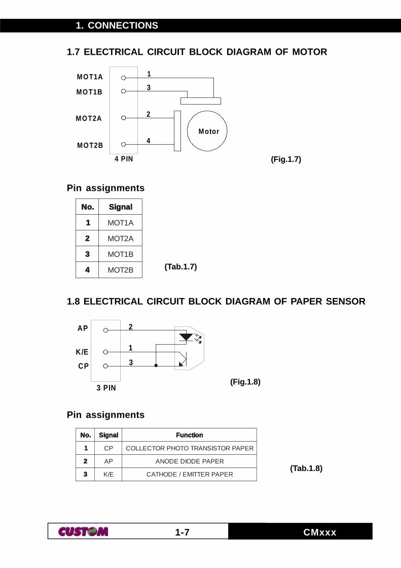
1.7 ELECTRICAL CIRCUIT BLOCK DIAGRAM OF MOTOR
Pin assignments
1.8 ELECTRICAL CIRCUIT BLOCK DIAGRAM OF PAPER SENSOR
Pin assignments
.oN .oN .oN .oN .oN langiS langiS langiS langiS langiS noitcnuF noitcnuF noitcnuF noitcnuF noitcnuF
11111 PC REPAPROTSISNARTOTOHPROTCELLOC
22222 PA REPAPEDOIDEDONA
33333 E/K REPAPRETTIME/EDOHTAC(Tab.1.8)
(Fig.1.8)
(Tab.1.7)
(Fig.1.7)
.oN .oN .oN .oN .oN langiS langiS langiS langiS langiS
11111 A1TOM
22222 A2TOM
33333 B1TOM
44444 B2TOM

1. CONNECTIONS
CMxxx 1-8
1
2SW 1
SW 2
2 PIN
1.9 ELECTRICAL CIRCUIT BLOCK DIAGRAM OF HEAD UPSENSOR
Pin assignments
.oN .oN .oN .oN .oN langiS langiS langiS langiS langiS noitcnuF noitcnuF noitcnuF noitcnuF noitcnuF
11111 1WS 1LANGISHCTIWS
22222 2WS 2LANGISHCTIWS(Tab.1.9)
(Fig.1.9)

2. PRINT HEAD
CMxxx2-1
2.1 PRINT HEAD
CMxxx has a thickfilm thermal printhead. Scanning Line Time (SLT) is thetime to print one complete line using all strobes available.The relation between the printhead supply voltage and “On Time” (Ton) is asfollows:
oI=oP 2 =vaRxdaeHV 2 vaRx
)ciR+vaR( 2
=noToE
oP
2.2 OPERATION PRECAUTIONS
1. When continuous printing is performed the supply energy should bereduced so that the substrate temperature show in Maximum ConditionTable
2. Power On and Off sequence must be in the following order to prevent thedot element damage: Turn On= Apply the logic supply voltage (Vdd) firstand then the printhead supply voltage. Turn Off= Switch off the printheadsupply voltage first and then turn the logic voltage off.
3. The printhead shall be disabled in STB during Power ON/OFF, or Power(VH)-Logic(Vdd) sequence described in note 2 shall be kept.
4. Heat elements and IC’s shall be anti-electrostatic in order to prevent theelectrostatic destruction. Do not touch the connector pins with nakedhands.
5. The printhead substrate surface is coated with glass and mechanicalstress or shock (including dust scratch damage) should be avoided toprevent damage.
6. When the printhead operation is finished, printsupply voltage (includingthe charged voltage with capacitor) should be reduced to the ground leveland remained until next printhead operation occur.
7. Condensation should be avoided. If condensation occurred, do not switchon the printhead power until condensation disappear.
8. If printing sound, for example sticking sound, occured, please adjust thepaper feed speed or pulse to avoid these kind of mechanical resonance.
9. Please pay attention that the paper used does not include bad factor toaffect printhead life.
(Tab.2.1)
lobmyS lobmyS lobmyS lobmyS lobmyS retemaraP retemaraP retemaraP retemaraP retemaraP tinU tinU tinU tinU tinU
vaR ecnatsiseregarevA 007 Ω
ciR ecnatsiseRdetarutaSrevirD 32 Ω

2. PRINT HEAD
CMxxx 2-2
10. The print density variation may become larger if the number of dotsenergized at same time becomes greater than the values specified in thetable 2.2 :
metI metI metI metI metI 85MC 85MC 85MC 85MC 85MC 06MC 06MC 06MC 06MC 06MC 08MC 08MC 08MC 08MC 08MC 211MC 211MC 211MC 211MC 211MC 012MC 012MC 012MC 012MC 012MC 612MC 612MC 612MC 612MC 612MC
stodforebmunmumixaMemitatadetavitca
821 291 291 652 844 844
2.3 ELECTRICAL CHARACTERISTICS OF CMxxx SERIES CIRCUIT2.3.1 CM58 Table
metI metI metI metI metI LOBMYS LOBMYS LOBMYS LOBMYS LOBMYS INIM INIM INIM INIM INIM .PYT .PYT .PYT .PYT .PYT .IXAM .IXAM .IXAM .IXAM .IXAM tinU tinU tinU tinU tinU
ylppusrewopdaeH HV 5.32 0.42 5.42 V
ylppusrewopcigoL ddV 57.4 0.5 52.5 V
tnerrucylppuscigoL ddI - - 72 Am
)hgiH(egatloVtupnI HIV ddVx8.0 - ddV V
)woL(egatloVtupnI LIV 0 - 2.0 x ddV V
hgiH)ID(tnerructupniataD )1( )1( )1( )1( )1( IDHLI - - 5.0 Au
woL)ID(tnerructupniataD IDLLI - - 5.0- Au
)hgiH(tnerructupni3ot1BTS )1( )1( )1( )1( )1( RTSHII - - 1 Au
)woL(tnerructupni3ot1BTS RTSLII - - 011- Au
)hgiH(tnerructupnikcolC )1( )1( )1( )1( )1( KLCHLI - - 3 Au
)woL(tnerructupnikcolC KLCLLII - - 3- Au
)hgiH(tnerructupnihctaL )1( )1( )1( )1( )1( TALHII - - 3 Au
)woL(tnerructupnihctaL TALLII - - 3- Au
)hgiH(egatlovtuptuotuoataD HODV 54.4 - - V
)woL(egatlovtuptuotuoataD LODV - 3.1 0.2 V
ycneuqerfkcolC f KLC 1.0 0.1 5.3 zHM
(1) Note: Each strobe includes pull-up resistance of 300KΩ ± 50%.
(Tab.2.3)
(Tab.2.2)
2. PRINT HEAD
CMxxx2-3
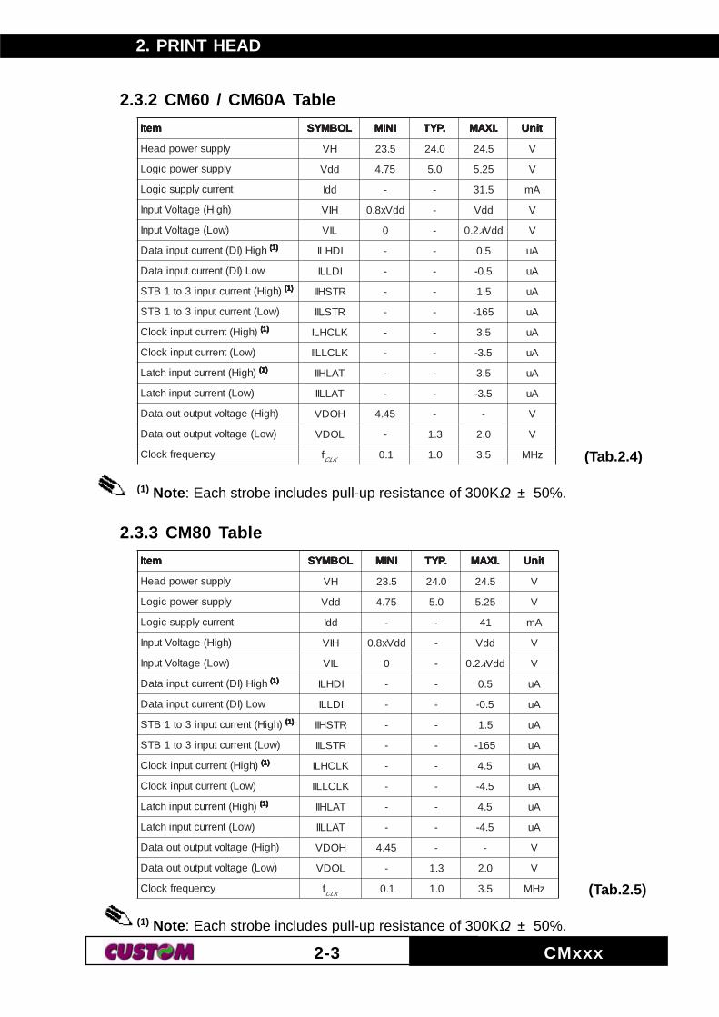
2.3.2 CM60 / CM60A Table
metI metI metI metI metI LOBMYS LOBMYS LOBMYS LOBMYS LOBMYS INIM INIM INIM INIM INIM .PYT .PYT .PYT .PYT .PYT .IXAM .IXAM .IXAM .IXAM .IXAM tinU tinU tinU tinU tinU
ylppusrewopdaeH HV 5.32 0.42 5.42 V
ylppusrewopcigoL ddV 57.4 0.5 52.5 V
tnerrucylppuscigoL ddI - - 5.13 Am
)hgiH(egatloVtupnI HIV ddVx8.0 - ddV V
)woL(egatloVtupnI LIV 0 - 2.0 x ddV V
hgiH)ID(tnerructupniataD )1( )1( )1( )1( )1( IDHLI - - 5.0 Au
woL)ID(tnerructupniataD IDLLI - - 5.0- Au
)hgiH(tnerructupni3ot1BTS )1( )1( )1( )1( )1( RTSHII - - 5.1 Au
)woL(tnerructupni3ot1BTS RTSLII - - 561- Au
)hgiH(tnerructupnikcolC )1( )1( )1( )1( )1( KLCHLI - - 5.3 Au
)woL(tnerructupnikcolC KLCLLII - - 5.3- Au
)hgiH(tnerructupnihctaL )1( )1( )1( )1( )1( TALHII - - 5.3 Au
)woL(tnerructupnihctaL TALLII - - 5.3- Au
)hgiH(egatlovtuptuotuoataD HODV 54.4 - - V
)woL(egatlovtuptuotuoataD LODV - 3.1 0.2 V
ycneuqerfkcolC f KLC 1.0 0.1 5.3 zHM
(1) Note: Each strobe includes pull-up resistance of 300KΩ ± 50%.
2.3.3 CM80 Table
metI metI metI metI metI LOBMYS LOBMYS LOBMYS LOBMYS LOBMYS INIM INIM INIM INIM INIM .PYT .PYT .PYT .PYT .PYT .IXAM .IXAM .IXAM .IXAM .IXAM tinU tinU tinU tinU tinU
ylppusrewopdaeH HV 5.32 0.42 5.42 V
ylppusrewopcigoL ddV 57.4 0.5 52.5 V
tnerrucylppuscigoL ddI - - 14 Am
)hgiH(egatloVtupnI HIV ddVx8.0 - ddV V
)woL(egatloVtupnI LIV 0 - 2.0 x ddV V
hgiH)ID(tnerructupniataD )1( )1( )1( )1( )1( IDHLI - - 5.0 Au
woL)ID(tnerructupniataD IDLLI - - 5.0- Au
)hgiH(tnerructupni3ot1BTS )1( )1( )1( )1( )1( RTSHII - - 5.1 Au
)woL(tnerructupni3ot1BTS RTSLII - - 561- Au
)hgiH(tnerructupnikcolC )1( )1( )1( )1( )1( KLCHLI - - 5.4 Au
)woL(tnerructupnikcolC KLCLLII - - 5.4- Au
)hgiH(tnerructupnihctaL )1( )1( )1( )1( )1( TALHII - - 5.4 Au
)woL(tnerructupnihctaL TALLII - - 5.4- Au
)hgiH(egatlovtuptuotuoataD HODV 54.4 - - V
)woL(egatlovtuptuotuoataD LODV - 3.1 0.2 V
ycneuqerfkcolC f KLC 1.0 0.1 5.3 zHM
(1) Note: Each strobe includes pull-up resistance of 300KΩ ± 50%.
(Tab.2.4)
(Tab.2.5)
2. PRINT HEAD
CMxxx 2-4
2.3.4 CM112 Table
metI metI metI metI metI LOBMYS LOBMYS LOBMYS LOBMYS LOBMYS INIM INIM INIM INIM INIM .PYT .PYT .PYT .PYT .PYT .IXAM .IXAM .IXAM .IXAM .IXAM tinU tinU tinU tinU tinU
ylppusrewopdaeH HV 5.32 0.42 5.42 V
ylppusrewopcigoL ddV 57.4 0.5 52.5 V
tnerrucylppuscigoL ddI - - 95 Am
)hgiH(egatloVtupnI HIV ddVx8.0 - ddV V
)woL(egatloVtupnI LIV 0 - 2.0 x ddV V
hgiH)ID(tnerructupniataD )1( )1( )1( )1( )1( IDHLI - - 5.0 Au
woL)ID(tnerructupniataD IDLLI - - 5.0- Au
)hgiH(tnerructupni4ot1BTS )1( )1( )1( )1( )1( RTSHII - - 2 Au
)woL(tnerructupni4ot1BTS RTSLII - - 022- Au
)hgiH(tnerructupnikcolC )1( )1( )1( )1( )1( KLCHLI - - 5.6 Au
)woL(tnerructupnikcolC KLCLLII - - 5.6- Au
)hgiH(tnerructupnihctaL )1( )1( )1( )1( )1( TALHII - - 5.6 Au
)woL(tnerructupnihctaL TALLII - - 5.6- Au
)hgiH(egatlovtuptuotuoataD HODV 54.4 - - V
)woL(egatlovtuptuotuoataD LODV - 3.1 0.2 V
ycneuqerfkcolC f KLC 1.0 0.1 5.3 zHM
(1) Note: Each strobe includes pull-up resistance of 300KΩ ± 50%.
2.3.5 CM210/CM210A/CM216/CM216A Table
metI metI metI metI metI LOBMYS LOBMYS LOBMYS LOBMYS LOBMYS INIM INIM INIM INIM INIM .PYT .PYT .PYT .PYT .PYT .IXAM .IXAM .IXAM .IXAM .IXAM tinU tinU tinU tinU tinU
ylppusrewopdaeH HV 5.32 0.42 5.42 V
ylppusrewopcigoL ddV 57.4 0.5 52.5 V
tnerrucylppuscigoL ddI - - 221 Am
)hgiH(egatloVtupnI HIV ddVx8.0 - ddV V
)woL(egatloVtupnI LIV 0 - 2.0 x ddV V
hgiH)ID(tnerructupniataD )1( )1( )1( )1( )1( IDHLI - - 5.0 Au
woL)ID(tnerructupniataD IDLLI - - 5.0- Au
)hgiH(tnerructupni4ot1BTS )1( )1( )1( )1( )1( RTSHII - - 5.3 Au
)woL(tnerructupni4ot1BTS RTSLII - - 583- Au
)hgiH(tnerructupnikcolC )1( )1( )1( )1( )1( KLCHLI - - 5.31 Au
)woL(tnerructupnikcolC KLCLLII - - 5.31- Au
)hgiH(tnerructupnihctaL )1( )1( )1( )1( )1( TALHII - - 5.31 Au
)woL(tnerructupnihctaL TALLII - - 5.31- Au
)hgiH(egatlovtuptuotuoataD HODV 54.4 - - V
)woL(egatlovtuptuotuoataD LODV - 3.1 0.2 V
ycneuqerfkcolC f KLC 1.0 0.1 5.3 zHM
(1) Note: Each strobe includes pull-up resistance of 300KΩ ± 50%.
(Tab.2.7)
(Tab.2.6)
2. PRINT HEAD
CMxxx2-5
CL O CK
DA TA IN
LA TC H
STRO BE
OU TPUTVO LT AG E
tw(T )
tsu(D ) th(D )
tsu(L A )
tw(L A)
tpLHtpHL
tsu(ST B )
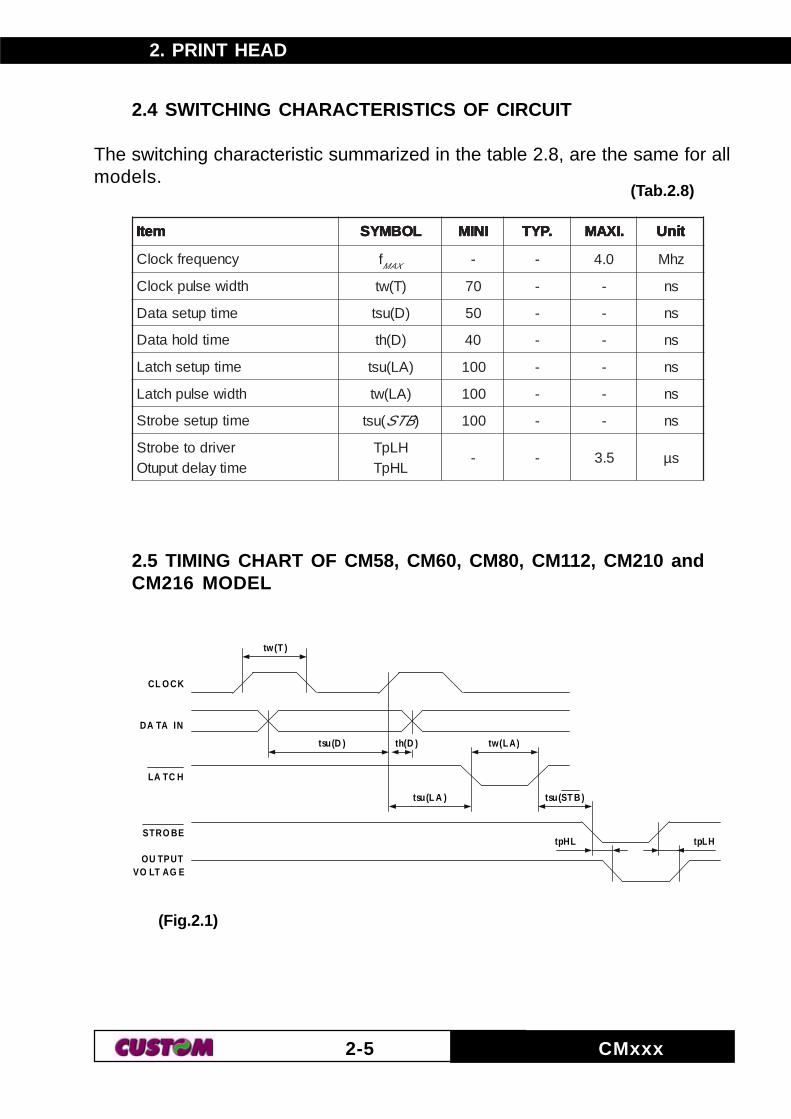
2.4 SWITCHING CHARACTERISTICS OF CIRCUIT
The switching characteristic summarized in the table 2.8, are the same for allmodels.
metI metI metI metI metI LOBMYS LOBMYS LOBMYS LOBMYS LOBMYS INIM INIM INIM INIM INIM .PYT .PYT .PYT .PYT .PYT .IXAM .IXAM .IXAM .IXAM .IXAM tinU tinU tinU tinU tinU
ycneuqerfkcolC f XAM - - 0.4 zhM
htdiweslupkcolC )T(wt 07 - - sn
emitputesataD )D(ust 05 - - sn
emitdlohataD )D(ht 04 - - sn
emitputeshctaL )AL(ust 001 - - sn
htdiwesluphctaL )AL(wt 001 - - sn
emitputesebortS (ust BTS ) 001 - - sn
revirdotebortSemityaledtuputO
HLpTLHpT
- - 5.3 µs
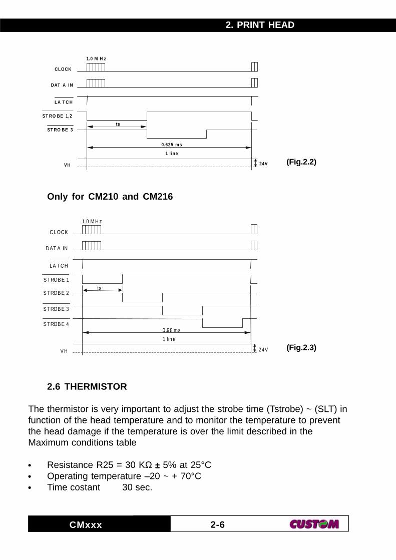
2.5 TIMING CHART OF CM58, CM60, CM80, CM112, CM210 andCM216 MODEL
(Fig.2.1)
(Tab.2.8)
2. PRINT HEAD
CMxxx 2-6
CLOCK
DAT A IN
VH
ST RO BE 3
ST RO BE 1,2
LA T C H
0.625 ms
1 l ine
ts
24V
1.0 M H z
C LOCK
D AT A IN
V H
S TROB E 2
S TROB E 1
LA TC H
0.98 ms
1 lin e
ts
24V
1.0 M H z
S TROB E 3
S TROB E 4
Only for CM210 and CM216
2.6 THERMISTOR
The thermistor is very important to adjust the strobe time (Tstrobe) ~ (SLT) infunction of the head temperature and to monitor the temperature to preventthe head damage if the temperature is over the limit described in theMaximum conditions table
••••• Resistance R25 = 30 KΩ ±±±±± 5% at 25°C••••• Operating temperature –20 ~ + 70°C••••• Time costant 30 sec.
(Fig.2.2)
(Fig.2.3)
2. PRINT HEAD
CMxxx2-7
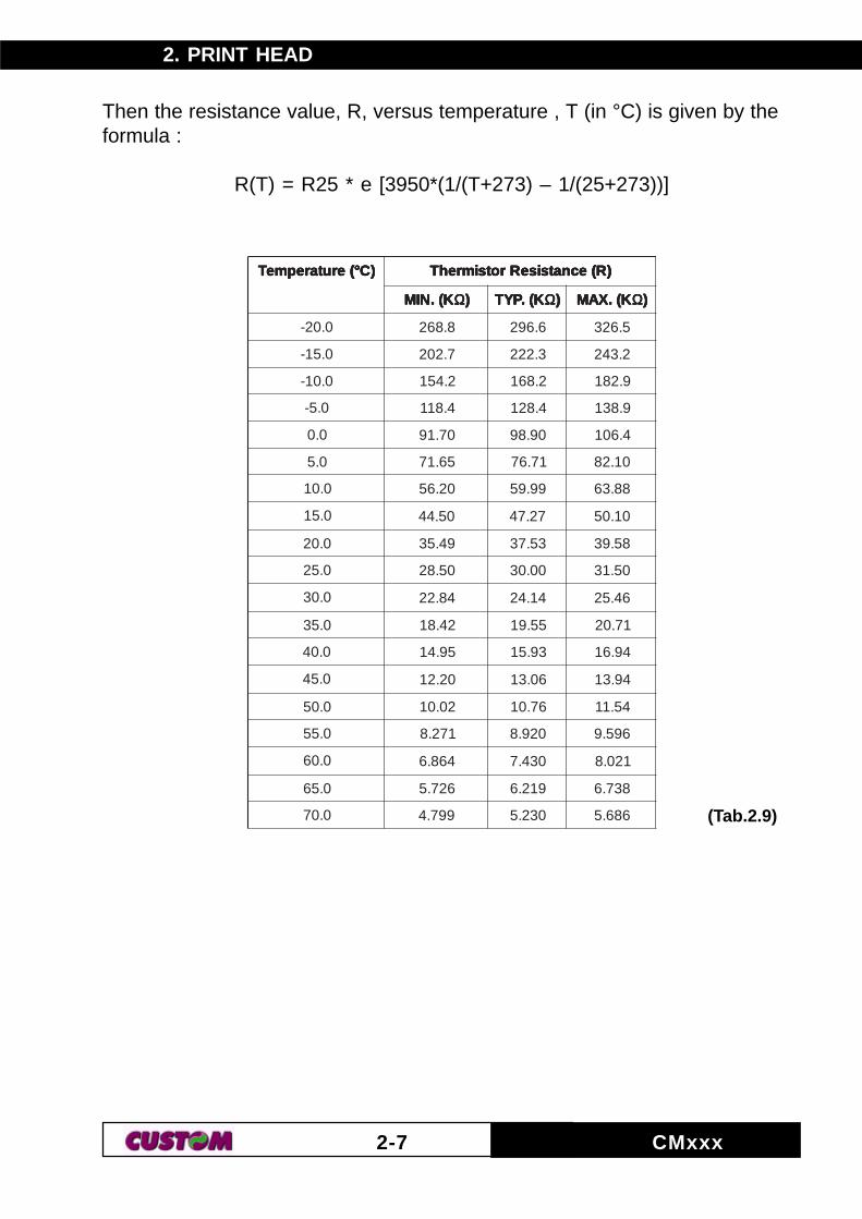
Then the resistance value, R, versus temperature , T (in °C) is given by theformula :
R(T) = R25 * e [3950*(1/(T+273) – 1/(25+273))]
)C°(erutarepmeT )C°(erutarepmeT )C°(erutarepmeT )C°(erutarepmeT )C°(erutarepmeT )R(ecnatsiseRrotsimrehT )R(ecnatsiseRrotsimrehT )R(ecnatsiseRrotsimrehT )R(ecnatsiseRrotsimrehT )R(ecnatsiseRrotsimrehT
K(.NIM K(.NIM K(.NIM K(.NIM K(.NIM ΩΩΩΩΩ))))) K(.PYT K(.PYT K(.PYT K(.PYT K(.PYT ΩΩΩΩΩ))))) K(.XAM K(.XAM K(.XAM K(.XAM K(.XAM ΩΩΩΩΩ)))))
0.02- 8.862 6.692 5.623
0.51- 7.202 3.222 2.342
0.01- 2.451 2.861 9.281
0.5- 4.811 4.821 9.831
0.0 07.19 09.89 4.601
0.5 56.17 17.67 01.28
0.01 02.65 99.95 88.36
0.51 05.44 72.74 01.05
0.02 94.53 35.73 85.93
0.52 05.82 00.03 05.13
0.03 48.22 41.42 64.52
0.53 24.81 55.91 17.02
0.04 59.41 39.51 49.61
0.54 02.21 60.31 49.31
0.05 20.01 67.01 45.11
0.55 172.8 029.8 695.9
0.06 468.6 034.7 120.8
0.56 627.5 912.6 837.6
0.07 997.4 032.5 686.5 (Tab.2.9)

2. PRINT HEAD
CMxxx 2-8
0,000
50,000
100,000
150,000
200,000
250,000
300,000
350,000-2
0,00
-15,
00
-10,
00
-5,0
0
0,00
5,00
10,0
0
15,0
0
20,0
0
25,0
0
30,0
0
35,0
0
40,0
0
45,0
0
50,0
0
55,0
0
60,0
0
65,0
0
70,0
0
Temperature (°C
Res
ista
nce
(K
Oh
m)
2.6.1 Thermistore Curves(Fig.2.4)

3. STEPPER MOTOR
CMxxx3-1
3.1 STEPPER MOTOR
The paper feed pitch for stepper motor is :- 1 step for one dotline(1) for the CM58, CM60 and CM112 model;- 2 steps for one dotline(1) for the CM210 and CM216 model.
(1) Note: 1 dotline = 0.125 mm.
metI metI metI metI metI noitacificepS noitacificepS noitacificepS noitacificepS noitacificepS
egatlovevirD egatlovevirD egatlovevirD egatlovevirD egatlovevirD V42CD
edomevirD edomevirD edomevirD edomevirD edomevirD evirdralopiB
euqrottuolluP euqrottuolluP euqrottuolluP euqrottuolluP euqrottuolluP g1.613 ⋅ NIMmc
deepswelsxaM deepswelsxaM deepswelsxaM deepswelsxaM deepswelsxaM NIMspp0011
ecnatsisergnidniW ecnatsisergnidniW ecnatsisergnidniW ecnatsisergnidniW ecnatsisergnidniW 9Ω C°52ta%01±
ecnatcudnignidniW ecnatcudnignidniW ecnatcudnignidniW ecnatcudnignidniW ecnatcudnignidniW )smrV1.zHk1(Hm9
ecnatsisernoitalusnI ecnatsisernoitalusnI ecnatsisernoitalusnI ecnatsisernoitalusnI ecnatsisernoitalusnI M001 Ω NIM
htgnertscirtceleiD htgnertscirtceleiD htgnertscirtceleiD htgnertscirtceleiD htgnertscirtceleiD .kaeletunim1*V005CA
efiL efiL efiL efiL efiL NIM.h0008
erutarepmetliocmumixaM erutarepmetliocmumixaM erutarepmetliocmumixaM erutarepmetliocmumixaM erutarepmetliocmumixaM C°511
CMxxx switching sequence (viewed from mounting surface)
roloC roloC roloC roloC roloC rotoM rotoM rotoM rotoM rotoM
kcalB kcalB kcalB kcalB kcalB 1A1A1A1A1A
nworB nworB nworB nworB nworB 3A3A3A3A3A
egnarO egnarO egnarO egnarO egnarO 1B1B1B1B1B
wolleY wolleY wolleY wolleY wolleY 3B3B3B3B3B
roloC roloC roloC roloC roloCkcalB kcalB kcalB kcalB kcalB nworB nworB nworB nworB nworB egnarO egnarO egnarO egnarO egnarO wolleY wolleY wolleY wolleY wolleY
petS petS petS petS petS
11111 ----- +++++ +++++ -----
22222 ----- +++++ ----- +++++
33333 +++++ ----- ----- +++++
44444 +++++ ----- +++++ -----
MotorLead Termination
(Tab.3.3)
(Tab.3.1)
(Fig.3.1)(Tab.3.2)
(Fig.3.2)

3. STEPPER MOTOR
CMxxx 3-2
3.1.1 Dynamic torque characteristics
ycneuqerF ycneuqerF ycneuqerF ycneuqerF ycneuqerF)spp(
tuo-lluP tuo-lluP tuo-lluP tuo-lluP tuo-lluP)mN4-^01(
ni-lluP ni-lluP ni-lluP ni-lluP ni-lluP)mN4-^01(
tnerruC tnerruC tnerruC tnerruC tnerruC)Am(
002 2.795 3.695 9513
004 4.936 1.205 2822
006 7.874 1.904 4261
008 2.593 3.413 7411
0001 7.913 7.712 638
0021 7.711 0.0 186
3.2 PRECAUTION
Precaution :
1. To prevent stepper motor over temperature, CUSTOM ENGINEERITNGSPA recommends to drive the motor with a PWM current control circuit.
(Tab.3.4)

4. SENSOR
CMxxx14-
4.1 SENSOR
Absolute Maximum Ratings (Ta = 25°C)
retemaraP retemaraP retemaraP retemaraP retemaraP lobmyS lobmyS lobmyS lobmyS lobmyS gnitaR gnitaR gnitaR gnitaR gnitaR tinU tinU tinU tinU tinU
tupnI tupnI tupnI tupnI tupnI
tnerrucdrawroF IIIIIF 05 Am
egatlovesreveR VVVVVRRRRR 5 V
noitapissidrewoP PPPPP 57 Wm
tnerrucdrawrofkaeP001htdiwesluP µ≤ %1=elcycytud,s
IIIII PF 1 A
tuptuO tuptuO tuptuO tuptuO tuptuO
egatlovrettime-rotcelloC VVVVV OEC OEC OEC OEC OEC 03 V
egatlovrotcelloc-rettimE VVVVV OCE OCE OCE OCE OCE 5 V
tnerrucrotcelloC IIIIICCCCC 05 Am
noitapissidrewoprotcelloC PPPPPCCCCC 57 Wm
Electro-optical Characteristics (Ta = 25°C)
retemaraP retemaraP retemaraP retemaraP retemaraP lobmyS lobmyS lobmyS lobmyS lobmyS snoitidnoC snoitidnoC snoitidnoC snoitidnoC snoitidnoC .NIM .NIM .NIM .NIM .NIM .PYT .PYT .PYT .PYT .PYT .XAM .XAM .XAM .XAM .XAM tinU tinU tinU tinU tinU
tupnI tupnI tupnI tupnI tupnI
egatlovdrawroF VVVVVF IIIIIF Am02= - 2.1 6.1 V
tnerrucesreveR IIIIIRRRRR VVVVVR V5= - - 01 µA
htgnelevawkaeP λλλλλPPPPP- 049 - mn
tuptuO tuptuO tuptuO tuptuO tuptuO tnerruckradrotcelloC IIIII OEC OEC OEC OEC OEC VVVVV EC V01= - - 001 An
deepSemitesiR ttttt rrrrr VVVVV EC ,V2= IIIIIC 001= µA
RRRRRL K1= Ω- 02 - µs
emitllaF ttttt fffff - 02 - µs
tnerrucegakaeL IIIII DOEC DOEC DOEC DOEC DOEC IIIIIF ,Am02= VVVVV EC V5= - - 1 µA
(Tab.4.1)
(Tab.4.2)

4. SENSOR
CMxxx 24-
- 25 0 25 50 75 85 1000
10
20
30
40
50
60F
orw
ard
cu
rren
t I
( m
A )
F
Am bient te mperature T (°C )a
Am bient te mperature T (°C )a
0 2 5- 2 50
20
40
60
120
50 10075
80
100
85
P C
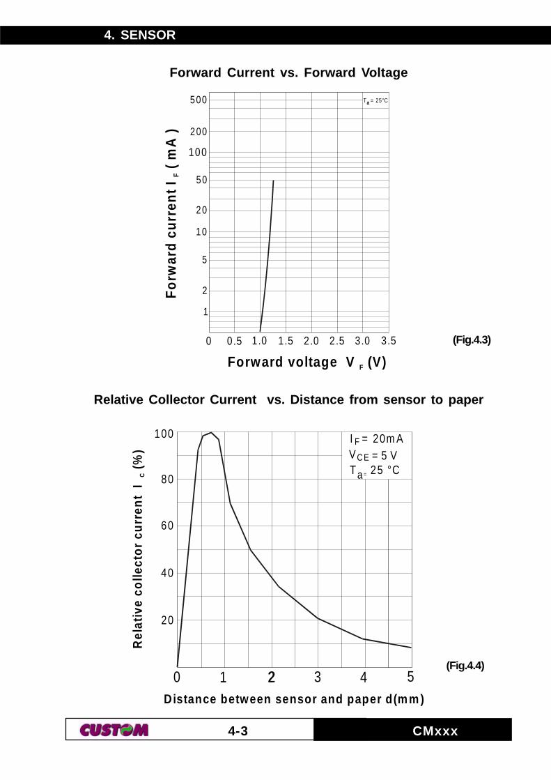
4.2 GRAPHICS OF TYPICAL CHARACTERISTICSForward Current vs. Ambient Temperature
Power Dissipation vs. Ambient Temperature
(Fig.4.1)
(Fig.4.2)
4. SENSOR
CMxxx34-
Fo
rwar
d c
urr
ent
I (
mA
)F
Forward voltage V (V)F
0 0.5 1.0 1.5 2.0 2.5 3.0 3.5
1
2
5
10
20
50
100
200
500 T = 25°Ca
0 2
20
40
60
80
3 541 2
100
T 25 °Ca =
I F = 20m AVCE = 5 V
Rel
ativ
e co
llect
or
curr
ent
I
(%
)C
D istance between sensor and paper d(m m )
(Fig.4.3)
(Fig.4.4)
Forward Current vs. Forward Voltage
Relative Collector Current vs. Distance from sensor to paper

5. DIMENSIONS
CMxxx15-
5.1 DIMENSIONS
The figure 5.1 illustrates the overall dimensions for the CM series thermalprinting mechanism.
LEDOM LEDOM LEDOM LEDOM LEDOM AAAAA BBBBB CCCCC DDDDD EEEEE
85MC 85MC 85MC 85MC 85MC 6.601 95 14 83 5.17
06MC 06MC 06MC 06MC 06MC 6.801 16 24 93 5.37
08MC 08MC 08MC 08MC 08MC 6.821 18 25 94 5.39
211MC 211MC 211MC 211MC 211MC 6.061 311 86 56 5.521
012MC 012MC 012MC 012MC 012MC 6.482 732 031 721 5.942
612MC 612MC 612MC 612MC 612MC 6.482 732 031 721 5.942
(Dimensions in mm)
(Tab.5.1)
FRONT VIEW
(Fig.5.1)TOP VIEW
LEFT SIDE VIEW


