
TI DCDC Solutions for Handheld and Low Standby Power Devices
Kean Pan
Business Development Engineer
1

TI Information – Selective Disclosure
Agenda
• Challenges for DCDC on Handheld / Low Power Devices
• DCS-Control Overview and Devices
• MicroSiP Modules
• Multi-phase DCDC for Processor Power
• DCDC for Multi-cell Application
• Ultra Low Power DCDC
2

TI Information – Selective Disclosure
Challenges for DCDC on Handheld / Low Power Devices
• Smaller solution size / higher power density
• Higher efficiency Extends operation time of application
Reduces overall system temperature
• Longer operating and stand-by time Active communication with application, e.g. DVS
Lower quiescent current, Snooze Mode
• Lower solution cost Less external components
Smaller external components
• Lower EMI and system noise No need for filtering
Supporting audio, optical and RF systems

TI Information – Selective Disclosure
4
DCS-Control Overview and Devices

TI Information – Selective Disclosure
DCS Control™ - Stands for
• High efficiency over the entire load current range
• Fastest load transient response
• Seamless transition into Power Save Mode
• Stable over a large range of output capacitance typ 10uF to 100uF
5

TI Information – Selective Disclosure
Traditional PWM Control Review
PFM Circuitry
OSC = Fixed Frequency
Internal Compensation
PFM Detection Circuitry
TI Information – Selective Disclosure
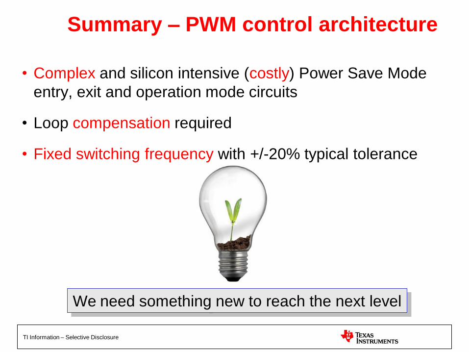
Summary – PWM control architecture
• Complex and silicon intensive (costly) Power Save Mode
entry, exit and operation mode circuits
• Loop compensation required
• Fixed switching frequency with +/-20% typical tolerance
We need something new to reach the next level

TI Information – Selective Disclosure
Basic Hysteretic Control
s
Vin Vout Vout ESRf
Vhys L Vin
Switching Frequency Varies and is
a Function of ESR, L and Vhys

TI Information – Selective Disclosure
Considerations – Hysteretic Control
• Possibly simplest control circuit
• Fastest response to input voltage and output voltage perturbations
among all control techniques
• Switching frequency depends on Vhys, L, Vin, Vout and ESR
– Frequency variation
• Inherently stable operation
• Modern DC DC converters have no output capacitor ESR
• Compensate for effects preventing good output voltage accuracy
• Implementation of Power Save Mode
• Control or acceptance of switching frequency variation
Technical items to be solved
Requires changes to basic hysteretic control

TI Information – Selective Disclosure
TPS62130 Block Diagram

TI Information – Selective Disclosure
DCS-Control™
Error Amplifier
for Precise DC
Regulation
Hysteretic
Comparator for
Fast Response
to Changes in
Output Voltage
Proprietary Ramp Circuitry Feeds VOS (Vout) to Comparator
On Timer for
Power Save Mode
and Constant
Operating
Frequency
FB
VOS (Vout)
Feedforward Capacitor
Only Required for Power
Save Mode Mode
Performance

TI Information – Selective Disclosure
What Does DCS-Control™ Provide?
•Superb Transient Response
•Seamless Transition To Power
Save Mode

TI Information – Selective Disclosure
Old versus DCS-Control™ Triangle Load Sweep (10mA – 1.0A)
TPS62110 TPS62150
CH1 – VOUT @ 50mV/div
CH2 – IL @ 1A/div
CH3 – ILOAD @ 1A/div
CH1 – VOUT @ 50mV/div
CH2 – IL @ 1A/div
CH3 – ILOAD @ 1A/div
No disturbing bursts during the transition
between PWM and Power Save Mode
Output voltage
Inductor Current
Load Current

TI Information – Selective Disclosure
How Does DCS-Control™ Go from Power Save Mode to PWM Mode?
DCS-Control™ = Direct Control with
Seamless Transition to Power Save Mode
Seamlessly!
Operating mode is the same in Power Save
Mode and PWM mode, so there is no mode
„switch‟ -> no possibility for glitch during mode
change

TI Information – Selective Disclosure
Inductor
Current
1A/div
SW node
Vout
50mV/div
Transition from Power Save Mode to PWM
Load Current
1A/div
Low Output Voltage Dip and Fast Recovery Time
&
Seamless Transition from Power Save Mode with No Overshoot
No load to 1A load step with 1uH and 22uF
~600 ns
~2% Vout

TI Information – Selective Disclosure
16
Standard Step down converter Portfolio 300mA-500mA
SOT23, 2x2
600mA
SOT23, 2x2
1A, 1.2A, 1.6A
MSOP, 2x2, 3x3
2A
2x2
3A
3x3
1st Generation L=4.7uH to 10uH
TPS62200
TPS62220
TPS62000
TPS62020
TPS62040
2nd Generation L=1.0uH to 2.2uH
TPS62240
TPS62270***
TPS62260
TPS62290
TPS62060
TPS62065
DCS Control™ L=1.0uH to 2.2uH
Cout up to 100uF
TPS62230
TPS62080 TPS62085* TPS62090
Value Devices TPS62560 TPS62590
TLV62080
TLV62065
TLV62090
TI Information – Selective Disclosure
17
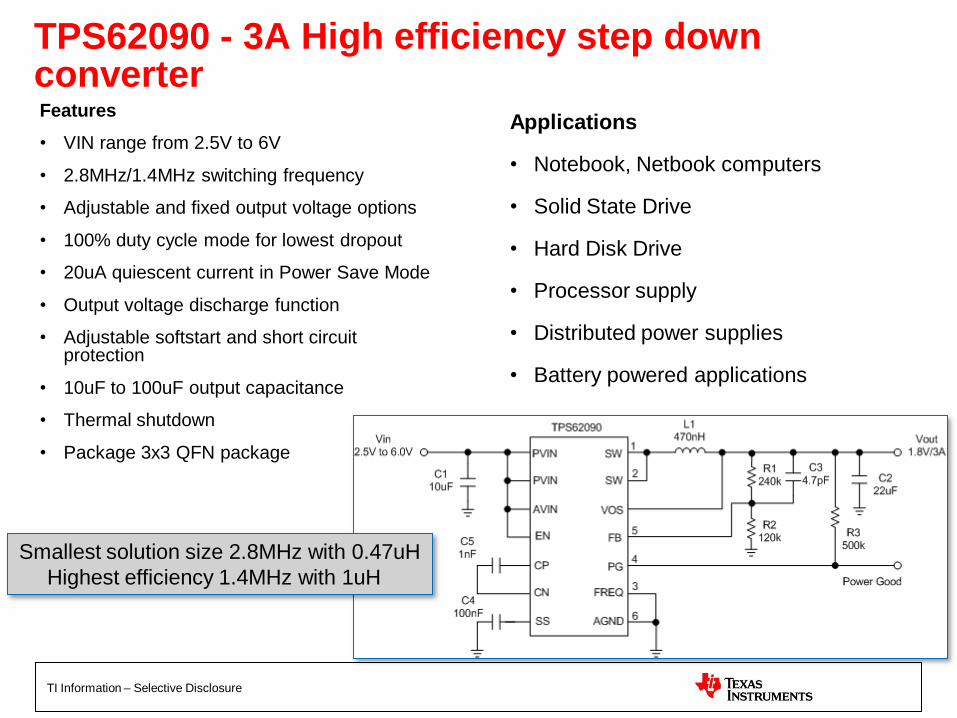
TPS62090 - 3A High efficiency step down converter Features
• VIN range from 2.5V to 6V
• 2.8MHz/1.4MHz switching frequency
• Adjustable and fixed output voltage options
• 100% duty cycle mode for lowest dropout
• 20uA quiescent current in Power Save Mode
• Output voltage discharge function
• Adjustable softstart and short circuit protection
• 10uF to 100uF output capacitance
• Thermal shutdown
• Package 3x3 QFN package
Applications
• Notebook, Netbook computers
• Solid State Drive
• Hard Disk Drive
• Processor supply
• Distributed power supplies
• Battery powered applications
Smallest solution size 2.8MHz with 0.47uH
Highest efficiency 1.4MHz with 1uH
TI Information – Selective Disclosure
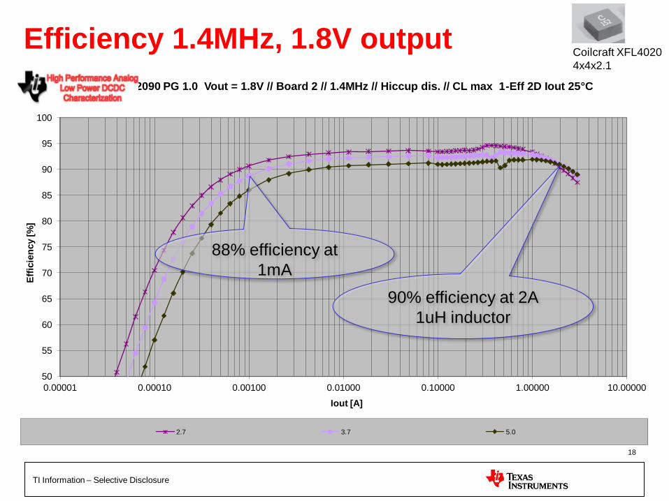
Efficiency 1.4MHz, 1.8V output
18
50
55
60
65
70
75
80
85
90
95
100
0.00001 0.00010 0.00100 0.01000 0.10000 1.00000 10.00000
Eff
icie
ncy [%
]
Iout [A]
TPS62090 PG 1.0 Vout = 1.8V // Board 2 // 1.4MHz // Hiccup dis. // CL max 1-Eff 2D Iout 25°C
2.7 3.7 5.0
90% efficiency at 2A
1uH inductor
88% efficiency at
1mA
Coilcraft XFL4020
4x4x2.1

TI Information – Selective Disclosure
Efficiency 2.8MHz, 1.8V output
19
50
55
60
65
70
75
80
85
90
95
100
0.00001 0.00010 0.00100 0.01000 0.10000 1.00000 10.00000
Eff
icie
ncy [%
]
Iout [A]
TPS62090 PG 1.0 Vout = 1.8V // Board 2 // 2.8MHz // Hiccup dis. // CL max 1-Eff 2D Iout 25°C
2.7 3.7 5.0
89% efficiency at 2A
400nH inductor
Coilcraft XFL4020
4x4x2.1

TI Information – Selective Disclosure
Fastest possible load transient response
20
Immediate and fastest
response to a load
step due to 100%
switch turn on
CH2:Vout, CH4=Iload, CH1=Inductor current
Load Step 0.2A to 2A

TI Information – Selective Disclosure
Seamless transition into Power Save Mode
21 CH2:Vout, CH3=Iload, CH4=Inductor current
Output voltage ripple
<20mV under all
conditions

TI Information – Selective Disclosure
Stable from 10uF up to 100uF output capacitance
22
CH2:Vout, CH4=Iload, CH1=Inductor current
1uH/10uF 1uH/100uF
Load Step 0.2A to 2A

TI Information – Selective Disclosure
23
TPS62080 – 1.2A High efficiency step down converter Features
• Vin range from 2.5V to 6V
• 3MHz switching frequency
• Adjustable and fixed output voltage options
• 100% duty cycle mode for lowest dropout
• 20uA quiescent current in Power Save Mode
• 6.5uA quiescent current in SNOOZE Mode
• Output voltage discharge function
• 10uF to 100uF output capacitance
• Thermal shutdown
• 3x3 QFN package
Applications
• Battery powered applications
• Distributed power supplies
• Notebook, Netbook computers
10% efficiency increase with
SNOOZE Mode

TI Information – Selective Disclosure
24
90% efficiency at 0.6A
1uH inductor
60% efficiency at
100uA in SNOOZE
Mode

TI Information – Selective Disclosure
TPS62080 load transient response
25
Only 25mV drop for
a 1A load step!

TI Information – Selective Disclosure
DCS Control™ - Stands for
• High efficiency over the entire load current range
• Fastest load transient response
• Seamless transition into Power Save Mode
• Stable over a large range of output capacitance typ 10uF to 100uF
26

MicroSiPTM DC/DC Converters
Fully Integrated Power Solutions

SiP … What is it all about?
1. Smallest solution size : Innovative 3D integration
2. Optimized electrical performance: Comparable efficiency,
lower EMI
3. Ease of use: Reduced HW design workload / application issues
4. One stop shopping
SiP stands for System in Package, i.e. a multiplicity of devices acting in concert
to perform one or more functions unattainable by a single (cost effective) device.
The package is the interconnect medium used to create a virtual “single” device.
A SiP approach can offer a significant number of advantages.
The advantages coming along with this technology can only be realized if:
- The rationale for doing the SiP meets certain criteria.
- There is a balance between SiP lamitate area vs. silicon size.

Order of Target Customer Preferences
1. Size
– Solution size >45% smaller
compared to discrete solution
– Less than 1mm height
2. Ease of Use
– No External Components needed
– Simplified PCB Layout
– One-Stop-Shop
3. Performance
– Superior EMI and noise
performance
– Similar feature set and efficiency
as discrete DC/DC converters
1 mm (max)
PicoStarTM
PicoStarTM
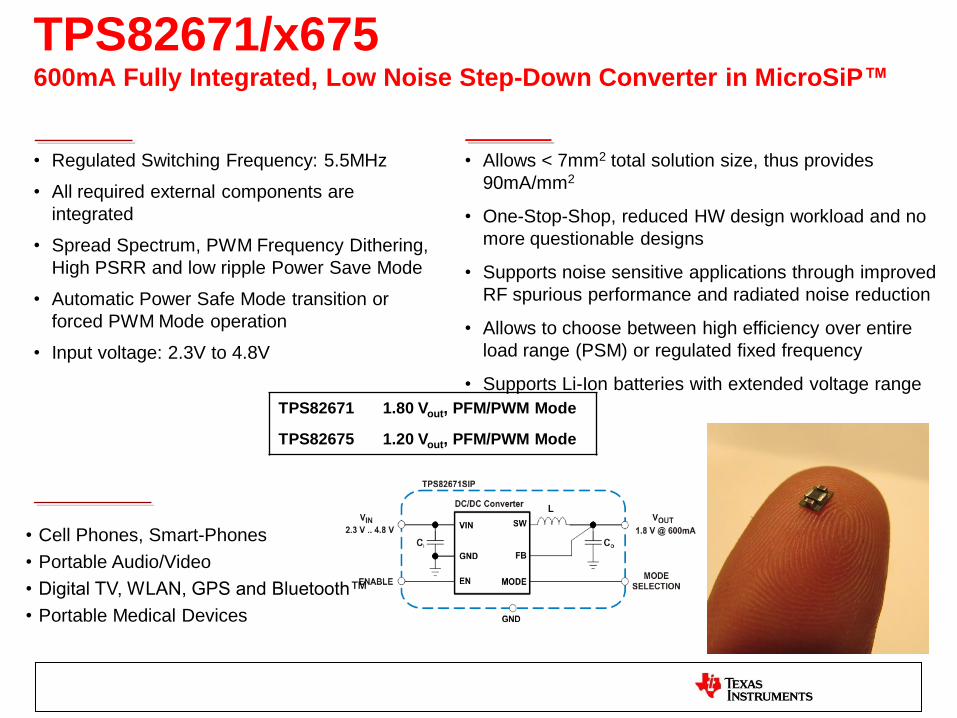
TPS82671/x675 600mA Fully Integrated, Low Noise Step-Down Converter in MicroSiP™
• Regulated Switching Frequency: 5.5MHz
• All required external components are
integrated
• Spread Spectrum, PWM Frequency Dithering,
High PSRR and low ripple Power Save Mode
• Automatic Power Safe Mode transition or
forced PWM Mode operation
• Input voltage: 2.3V to 4.8V
• Allows < 7mm2 total solution size, thus provides
90mA/mm2
• One-Stop-Shop, reduced HW design workload and no
more questionable designs
• Supports noise sensitive applications through improved
RF spurious performance and radiated noise reduction
• Allows to choose between high efficiency over entire
load range (PSM) or regulated fixed frequency
• Supports Li-Ion batteries with extended voltage range
TPS82671 1.80 Vout, PFM/PWM Mode
TPS82675 1.20 Vout, PFM/PWM Mode
• Cell Phones, Smart-Phones
• Portable Audio/Video
• Digital TV, WLAN, GPS and Bluetooth™
• Portable Medical Devices

MircoSiP™ Module Overview
Device Output
Voltage [V]
Supply Voltage
Range [V]
Output Current
[mA]
Features
TPS82676 1.10 2.3 – 4.8 600 PFM/PWM Mode, Output Cap Discharge, SSM
TPS82677 1.20 2.3 – 4.8 600 PWM Mode, Output Cap Discharge
TPS82674 1.20 2.3 – 4.8 600 PFM/PWM Mode, Output Cap Discharge, SSM
TPS82675 1.20 2.3 – 4.8 600 PFM/PWM Mode, SSM
TPS82673 1.26 2.3 – 4.8 600 PFM/PWM Mode, Output Cap Discharge, SSM
TPS82672 1.50 2.3 – 4.8 600 PFM/PWM Mode, SSM
TPS82671 1.80 2.3 – 4.8 600 PFM/PWM Mode, SSM
TPS826711 1.80 2.3 – 4.8 600 PFM/PWM Mode, Output Cap Discharge, SSM
TPS82670 1.86 2.3 – 4.8 600 PFM/PWM Mode, Output Cap Discharge, SSM
TPS82690 2.85 2.3 – 4.35 500 PFM/PWM Mode, Output Cap Discharge
TPS82695 2.50 2.3 – 4.35 500 PFM/PWM Mode, Output Cap Discharge
Step-Down Converter
Boost Converter
Device Output
Voltage [V]
Supply Voltage
Range [V]
Output Current
[mA]
Features
TPS81256 5.0 2.5 – 5.5 550+ PFM/PWM Mode, Load Disconnect
1 mm (max)
SSM = Spread Spectrum Modulation
TI Information – Selective Disclosure
Multi-phase DCDC for Processor Power
32

TI Information – Selective Disclosure
App Processor Trends
33
10
100
2002 2004 2006 2008 2010 2012
pro
cess
no
de
[nm
]
90nm
60nm
45nm
28nm
• Process node scaling
• Higher clock rates and SoC
integration
– Driven by performance need
– Marketing driven
• Reduced process scale:
– Increased leakage
– Higher process variation
– Reduced VDD and wider distribution
– Reduced parasitic gate capacitance
overcompensated by • Increased gate #
• Higher clock rates
• Battery technology – Does not keep pace
– New batteries:
• Ever increasing power demand
2
static dynamic DD Gate CR DDP P P f(V ) f(C ,#,f ,V )
TI Information – Selective Disclosure
Key Focus: High Efficiency Operation
Load Current
Eff
icie
nc
y
PFM Split Power Stage
PFM 1-ph Power Stage
PWM 1-ph Power Stage
PWM 2-ph Power Stages
• Ultra Light load: PFM split power stage. – Parasitic FET gate capacitance is kept at minimum number for lowest currents
• Light load: single phase PFM operation. – PFM maintains high efficiency conversion.
• Medium load: single phase PWM operation – Small RDS,on FETs keep efficiency high at medium loads
• High load: multi-phase PWM operation – Phases operate in parallel. The effective RDS,on is divided by the number of phases. In addition, losses in the inductor are kept as small as
possible since the DCR is divided as well.
• Incorporated Charge-Pump – Si-Anode low-VIN efficiency boost/ process variation /peak output current efficiency boost
→ high efficiency operation over the complete load range
TI Information – Selective Disclosure
Key Focus: Smallest Solution Size
• Smallest solution size is achieved by
– Stand-alone concept: compared to PMICs, decoupling caps can be saved, placement can be optimized
– Small input and output capacitors
– Cancelling additional external components
– Enabling smallest inductors • Single phase: allowing tiniest inductors
by high frequency operation and current limits optimized for choosing tiny inductors
• Multi phase: The multi-phase technology allows for choosing smallest inductors with small saturation currents. The overall size of the n inductors is smaller than a single inductor with an according saturation current would be. Still, smaller effective DCRs can be achieved keeping inductor losses small by putting them in parallel. Height requirements (<1.2mm, <1.0mm, <0.8mm) can be met.
35
Volume Factor 4 for 2x current.
½ I (0.47uH) vs. I (0.47uH)
Volume Factor 2 for 2x current for ½ inductance
½ I (0.47uH) vs. I (0.2uH)
TI Information – Selective Disclosure
Multi phase vs. two inductors in parallel
• DCR variation causes inductor current to be unequally distributed. A PCB temperature gradient might enforce this effect
– Efficiency suffers since the “seen” DCR is not DCR/2
– An inductor might run into saturation. A higher saturation current is required, increasing solution size
• No phase shedding feasible
• No phase inversed operation possible
• Regulation bandwidth limitation
36
• To achieve smallest solution size, tiny inductors are a must. Tiny inductors come with limited saturation current ratings. So why not putting simply two inductors in parallel to overcome height constrains?
• On TPS6238xx solutions, the current is actively balanced
• The efficiency benefits from both DCR and RDS,on in parallel reducing losses by 50% for two phases and by 66% for three phases
• Automatic phase shedding allows highest efficiency over the complete output current range
• The output voltage ripple is minimized by phase inverted operation
• EMI and input ripple are minimized by phase inverted operation
• The effective regulation bandwidth is increased with the number of phases
• Balancing and precise current limits allow the choice of tiniest inductors
TI Information – Selective Disclosure
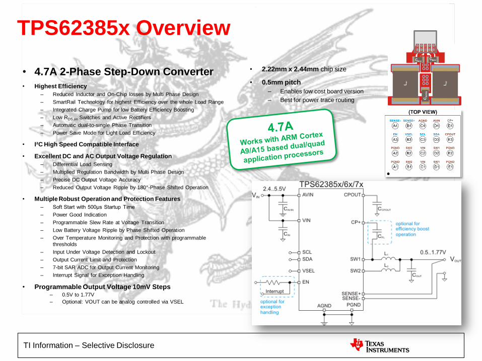
TPS62385x Overview
• 4.7A 2-Phase Step-Down Converter
• Highest Efficiency
– Reduced Inductor and On-Chip losses by Multi Phase Design
– SmartRail Technology for highest Efficiency over the whole Load Range
– Integrated Charge Pump for low Battery Efficiency Boosting
– Low RDS,on Switches and Active Rectifiers
– Automatic dual-to-single Phase Transition
– Power Save Mode for Light Load Efficiency
• I²C High Speed Compatible Interface
• Excellent DC and AC Output Voltage Regulation
– Differential Load Sensing
– Multiplied Regulation Bandwidth by Multi Phase Design
– Precise DC Output Voltage Accuracy
– Reduced Output Voltage Ripple by 180°-Phase Shifted Operation
• Multiple Robust Operation and Protection Features
– Soft Start with 500μs Startup Time
– Power Good Indication
– Programmable Slew Rate at Voltage Transition
– Low Battery Voltage Ripple by Phase Shifted Operation
– Over Temperature Monitoring and Protection with programmable
thresholds
– Input Under Voltage Detection and Lockout
– Output Current Limit and Protection
– 7-bit SAR ADC for Output Current Monitoring
– Interrupt Signal for Exception Handling
• Programmable Output Voltage 10mV Steps – 0.5V to 1.77V
– Optional: VOUT can be analog controlled via VSEL
• 2.22mm x 2.44mm chip size
• 0.5mm pitch
– Enables low cost board version
– Best for power trace routing

TI Information – Selective Disclosure
TPS62386x Overview
• 6.8A 2-Phase Step-Down Converter
• Highest Efficiency
– Reduced Inductor and On-Chip losses by Multi Phase Design
– SmartRail Technology for highest Efficiency over the whole Load Range
– Integrated Charge Pump for low Battery Efficiency Boosting
– Low RDS,on Switches and Active Rectifiers
– Automatic dual-to-single Phase Transition
– Power Save Mode for Light Load Efficiency
• I²C High Speed Compatible Interface
• Excellent DC and AC Output Voltage Regulation
– Differential Load Sensing
– Multiplied Regulation Bandwidth by Multi Phase Design
– Precise DC Output Voltage Accuracy
– Reduced Output Voltage Ripple by 180°-Phase Shifted Operation
• Multiple Robust Operation and Protection Features
– Soft Start with 500μs Startup Time
– Power Good Indication
– Programmable Slew Rate at Voltage Transition
– Low Battery Voltage Ripple by Phase Shifted Operation
– Over Temperature Monitoring and Protection with programmable
thresholds
– Input Under Voltage Detection and Lockout
– Output Current Limit and Protection
– 7-bit SAR ADC for Output Current Monitoring
– Interrupt Signal for Exception Handling
• Programmable Output Voltage 10mV Steps – 0.5V to 1.77V
– Optional: VOUT can be analog controlled via VSEL
• 2.22mm x 2.44mm chip size
• 0.5mm pitch
– Enables low cost board version
– Best for power trace routing

TI Information – Selective Disclosure
TPS62387x Overview
• 7.8A 2-Phase Step-Down Converter
• Highest Efficiency
– Reduced Inductor and On-Chip losses by Multi Phase Design
– SmartRail Technology for highest Efficiency over the whole Load Range
– Integrated Charge Pump for low Battery Efficiency Boosting
– Low RDS,on Switches and Active Rectifiers
– Automatic dual-to-single Phase Transition
– Power Save Mode for Light Load Efficiency
• I²C High Speed Compatible Interface
• Excellent DC and AC Output Voltage Regulation
– Differential Load Sensing
– Multiplied Regulation Bandwidth by Multi Phase Design
– Precise DC Output Voltage Accuracy
– Reduced Output Voltage Ripple by 180°-Phase Shifted Operation
• Multiple Robust Operation and Protection Features
– Soft Start with 500μs Startup Time
– Power Good Indication
– Programmable Slew Rate at Voltage Transition
– Low Battery Voltage Ripple by Phase Shifted Operation
– Over Temperature Monitoring and Protection with programmable
thresholds
– Input Under Voltage Detection and Lockout
– Output Current Limit and Protection
– 7-bit SAR ADC for Output Current Monitoring
– Interrupt Signal for Exception Handling
• Programmable Output Voltage 10mV Steps – 0.5V to 1.77V
– Optional: VOUT can be analog controlled via VSEL
• 2.22mm x 2.44mm chip size
• 0.5mm pitch
– Enables low cost board version
– Best for power trace routing
TI Information – Selective Disclosure
DCDC for Multi-Cell Applications
40

DCS-Control™ Step-Down Converter VIN MAX >6V
Vin Vout Iout L - C Package Solution Size
[mm2] *
Features
TPS62120 2.0 to 15V ADJ,
2.0V
75mA 22uH/4.7uF 3x3 SOT 30 Iq=11uA, EN, PG,
2x2 SON (TPS62122),
DCS-ControlTM
TPS62125 3.0 to 17V ADJ,
1.8V
300mA 10uH/10uF 2x2 SON 40 Iq=11uA, Adj. EN, PG,
DCS-ControlTM
TPS62130 3.0 to 17V ADJ, 1.8,
3.3, 5.0V
3.0 A 1uH/22uF 3x3 QFN 95 Iq=17uA, EN, PG,
FSW, DEF, SS/TR,
DCS-ControlTM
TPS62140 3.0 to 17V ADJ, 1.8,
3.3, 5.0V
2.0A 1uH/22uF 3x3 QFN 95 Iq=17uA, EN, PG,
FSW, DEF, SS/TR,
DCS-ControlTM
TPS62150 3.0 to 17V ADJ, 1.8,
3.3, 5.0V
1.0A 1uH/22uF 3x3 QFN 85 Iq=17uA, EN, PG,
FSW, DEF, SS/TR,
DCS-ControlTM
TPS62160 3.0 to 17V ADJ, 1.8,
3.3, 5.0V
1.0A 2.2uH/22uF 2x2 SON 45 Iq=17uA, EN, PG,
DCS-ControlTM
TPS62170 3.0 to 17V ADJ, 1.8,
3.3, 5.0V
0.5A 2.2uH/22uF 2x2 SON 45 Iq=17uA, EN, PG,
DCS-ControlTM
* Estimated Total Solution Size based on EVM layout for fixed VOUT, incl. CIN, COUT and L
Pin to Pin Compatible
Pin to Pin Compatible

TPS6216x/17x Tiny 17V 0.5A/1A Step-Down Converter in 2x2 WSON
• DCS-Control™ topology: fast AC line and load transient
response plus seamless transition into Power Save Mode
• Supports high Output Capacitance of up to 200uF
• Works with small inductor and low ESR capacitors
• 100% Duty Cycle and 17uA typ. Quiescent Current
• Power Good Output
• General Purpose Point-of-Load
• Industrial Applications, e.g. PLC, measurement
• DSC Camera
• Enterprise Solid-state drives
• Low power DSP core applications
• Computing
• Maintains a stable and accurate output voltage
• Robust design through supporting many L-C
combinations and on board capacitance
• Allows cost efficient external components and
supports a total solution size of 45mm2
• Enables extended application run time through
lowest dropout and power consumption
• Indicates output voltage condition, e.g. for
system communication like startup
sequencing.
Released:
November 2011
TPS62160EVM-627
TPS62170EVM-627

TI Information – Selective Disclosure
22uF
1.8V / 3A
10uF
1μH(3 .. 17)V
3.3nF
TPS62131
PVIN
AVIN
EN
SS/TR
DEF
FSW
SW
VOS
PG
FB
AGND
PGND
100k
TPS62130/40/50: 3 - 17V VIN, 1-3A, 2.5MHz Step-Down Converters in 3x3mm QFN
• General Purpose POL
• Solid State Disk Drives
• Embedded and mobile Computing
• Industrial applications
• High VIN step down converter with small solution size
• 12V @ 3.3V / 3A utilizing a 1uH inductor
• DCS-ControlTM regulation is fast and accurate
• Low quiescent current and selectable switching
frequency for high efficiency
• VFB control allows current source applications
• High Efficiency Step Down Converter with DCS-ControlTM
• VIN range from 3 to 17V
• Adjustable VOUT from 0.9 to 6.0V
• Fixed VOUT options: 1.8V, 3.3V, 5.0V
• Output current up to: 3A (TPS62130)
2A (TPS62140)
1A (TPS62150)
• Seamless transition to Power Save Mode
• Pin-selectable switching frequency (full, half)
• 100% Duty Cycle Mode
• Programmable Soft Start and Tracking
• Quiescent current of 17uA (typ.)
• Power Good
DEF Pin Selectable Output Voltage
FSW Pin Selectable Switching Frequency
Cstart Adjustable Startup
TR FB Voltage Control
TPS62130EVM-505
TPS62140EVM-505
TPS62150EVM-505
Released:
November 2011
TI Information – Selective Disclosure
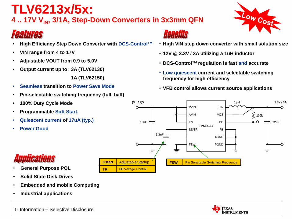
TLV6213x/5x: 4 .. 17V VIN, 3/1A, Step-Down Converters in 3x3mm QFN
• General Purpose POL
• Solid State Disk Drives
• Embedded and mobile Computing
• Industrial applications
• High VIN step down converter with small solution size
• 12V @ 3.3V / 3A utilizing a 1uH inductor
• DCS-ControlTM regulation is fast and accurate
• Low quiescent current and selectable switching
frequency for high efficiency
• VFB control allows current source applications
• High Efficiency Step Down Converter with DCS-ControlTM
• VIN range from 4 to 17V
• Adjustable VOUT from 0.9 to 5.0V
• Output current up to: 3A (TLV62130)
1A (TLV62150)
• Seamless transition to Power Save Mode
• Pin-selectable switching frequency (full, half)
• 100% Duty Cycle Mode
• Programmable Soft Start.
• Quiescent current of 17uA (typ.)
• Power Good
FSW Pin Selectable Switching Frequency Cstart Adjustable Startup
TR FB Voltage Control
22uF
1.8V / 3A
10uF
1μH(3 .. 17)V
3.3nF
TPS62131
PVIN
AVIN
EN
SS/TR
DEF
FSW
SW
VOS
PG
FB
AGND
PGND
100k
TI Information – Selective Disclosure
45
Ultra Low Power DC DC
Product Overview + Roadmap

TI Information – Selective Disclosure
46
Ultra Low Power - Product Status
• TPS62120 Industry's first commercial successful energy harvester in full production Iq=11uA
• CC430 solar demonstrator
• TPS61251 adjustable current limit boost converter with 2uA Snooze mode
• TPS62730 CC2540 Companion Step Cown Converter with 30nA standby mode
• TPS62125 300mA Step down Converter with 6uA EN comparator
47
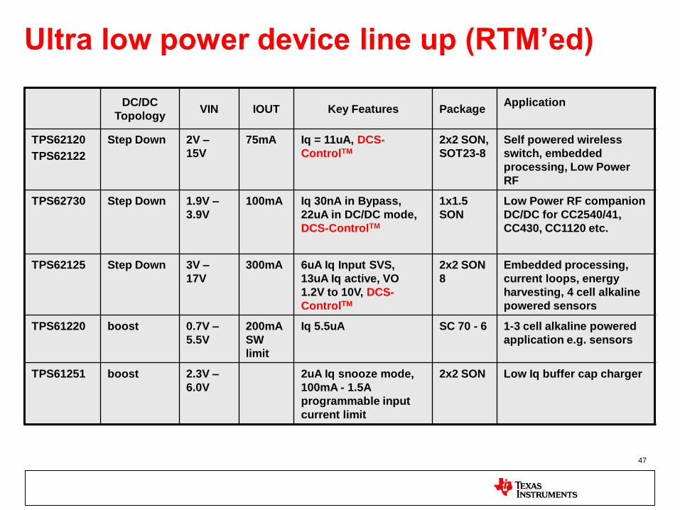
Ultra low power device line up (RTM’ed)
DC/DC
Topology VIN IOUT Key Features Package
Application
TPS62120
TPS62122
Step Down 2V –
15V
75mA Iq = 11uA, DCS-
ControlTM
2x2 SON,
SOT23-8
Self powered wireless
switch, embedded
processing, Low Power
RF
TPS62730 Step Down 1.9V –
3.9V
100mA Iq 30nA in Bypass,
22uA in DC/DC mode,
DCS-ControlTM
1x1.5
SON
Low Power RF companion
DC/DC for CC2540/41,
CC430, CC1120 etc.
TPS62125 Step Down 3V –
17V
300mA 6uA Iq Input SVS,
13uA Iq active, VO
1.2V to 10V, DCS-
ControlTM
2x2 SON
8
Embedded processing,
current loops, energy
harvesting, 4 cell alkaline
powered sensors
TPS61220 boost 0.7V –
5.5V
200mA
SW
limit
Iq 5.5uA SC 70 - 6 1-3 cell alkaline powered
application e.g. sensors
TPS61251 boost 2.3V –
6.0V
2uA Iq snooze mode,
100mA - 1.5A
programmable input
current limit
2x2 SON Low Iq buffer cap charger
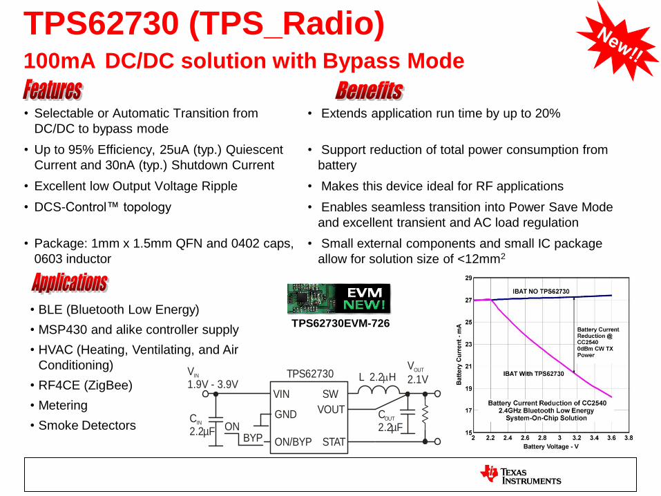
TPS62730 (TPS_Radio) 100mA DC/DC solution with Bypass Mode
• Selectable or Automatic Transition from
DC/DC to bypass mode
• Up to 95% Efficiency, 25uA (typ.) Quiescent
Current and 30nA (typ.) Shutdown Current
• Excellent low Output Voltage Ripple
• DCS-Control™ topology
• Package: 1mm x 1.5mm QFN and 0402 caps,
0603 inductor
• BLE (Bluetooth Low Energy)
• MSP430 and alike controller supply
• HVAC (Heating, Ventilating, and Air
Conditioning)
• RF4CE (ZigBee)
• Metering
• Smoke Detectors
• Extends application run time by up to 20%
• Support reduction of total power consumption from
battery
• Makes this device ideal for RF applications
• Enables seamless transition into Power Save Mode
and excellent transient and AC load regulation
• Small external components and small IC package
allow for solution size of <12mm2
TPS62730
VIN
ON/BYP STAT
GND VOUT
SW
V
2.1VOUTV
1.9V - 3.9VIN
C2.2
IN
µF
C2.2
OUT
µF
L 2.2 Hm
ONBYP
TPS62730EVM-726

TI Information – Selective Disclosure
High efficiency in PFM mode
2.5V Rising / 1.85V Falling UVLO Thresholds
, ,
,
Active Discharge Capacitor (TPS62120)
,
Power Good pin (TPS62120)
SOT-23-8 (TPS62120), 2x2 QFN (TPS62122)
Above 70% efficiency @ 100uA
Wide UVLO hysteresis window allows the storage of energy in
CIN until there is enough for the converter to efficiently transfer
to the output avoiding short cycling during buck power-up
Allows time control for power sequencing & a clear and sharp start
up voltage.
Notification of output voltage being regulated when Vout is greater
than 95% of the nominal value
Multiple solar cells
Inductive energy harvesters
Low Power RF Applications
Low Power Microprocessor
Industrial sensing (12V bus)
TPS62120, TPS62122 2V to 15V Input, 75mA Iout, 96% efficiency Step-Down Converter
TPS62122EVM-586
TPS62120EVM-640

TI Information – Selective Disclosure
High Efficiency
Above 70% @ 100µA for 10VIN

TI Information – Selective Disclosure
Proper start up from weak source
L
C4.7 F
OUT
µ
V =1.8VOUT
C 4.7
IN
Fµ
C 100
store
Fµ
5V300uASolarModule600Lux
Load100R
TPS62120 vs.TPS62231
TPS62120 UVLO hysteresis ~ 600mV TPS62231UVLO hysteresis ~100mV
Runtime ~ 4ms -> 130uWs Energy Runtime ~ 400us -> 13uWs
Larger UVLO Hysteresis more energy can be extracted from the storage capacitor

TPS62125 300-mA Step-Down Converter with Adjustable Enable Threshold and Hysteresis
• Adjustable ENABLE threshold and
hysteresis
• DCS-Control™ topology
• High efficiency over entire load and
supply voltage range
• Wide input voltage range: 3V - 17V
• 100% Duty Cycle for Lowest Dropout
• Energy Harvesting supplies
• Battery applications: 4x Alkaline or 2-4 Li-Ion cells
• 9V – 15V bus voltage rails
• Embedded Processing
• Inverter (negative VOUT)
• Extend application run-time through high design flexibility
• Maintains a stable output voltage through a fast AC line
and load transient response
• Increases Efficiency at very light loads (>60% at 100uA)
• Allows to capture the entire energy from the harvester;
tolerates multiple different supply types
• Achieves longest run-time by allowing the application to
operate close to the input voltage level
Released:
May 2012
TPS62125EVM-044

TI Information – Selective Disclosure
TPS62125 Programmable EN Comparator
VIN
REF
ON/SHDN VREF
EN
EN_hys
GND
VIN
ENComparator
REN1
REN2
REN HYS
Precise (3%) programmable start up threshold setting
Only 6uA quiescent current consumption
EN comparator with internal 50mV hysteresis
Increasing hysteresis with external resistor on EN-hys pin
VINVIN_startup
VIN_stop
VOUT
Hysteresis
DC/DC ON
DC/DC OFF
Proper VOUT ramp up

TI Information – Selective Disclosure
Thank you
54


![DCDC converters slides.ppt [Lecture seule] [Mode de ...steel-electronique.fr/files/steel/produits/DCDC-converters-slides-0a.pdf · DC/DC converters « Off the shelf » STEEL ELECTRONIQUE](https://cdn.vdocuments.net/doc/165x107/5eacbacc2d1b267771770dbd/dcdc-converters-lecture-seule-mode-de-steel-electroniquefrfilessteelproduitsdcdc-converters-slides-0apdf.jpg)


