1
2
3
4
5
6
7
8
16
15
14
13
12
11
10
9
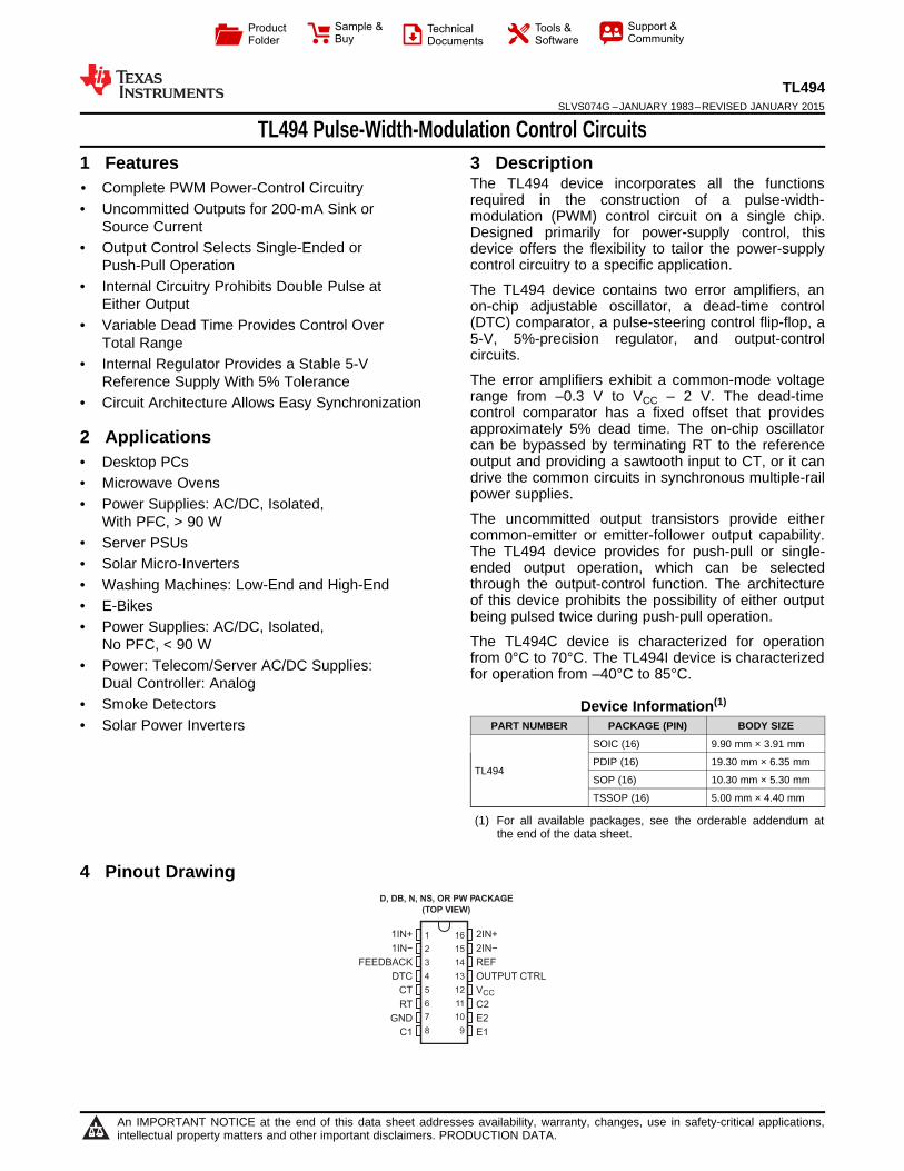
1IN+
1IN−
FEEDBACK
DTC
CT
RT
GND
C1
2IN+
2IN−
REF
OUTPUT CTRL
VCC
C2
E2
E1
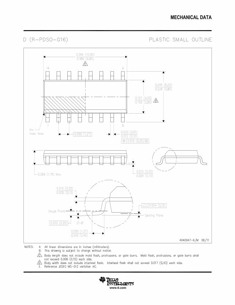
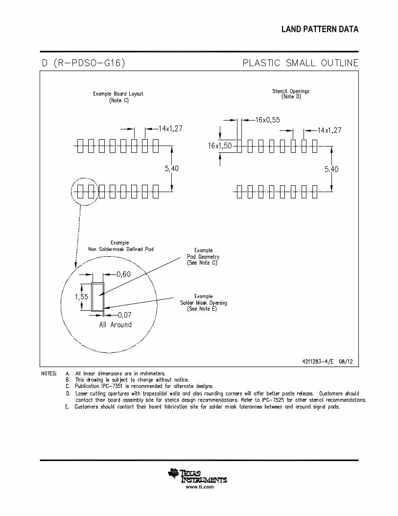
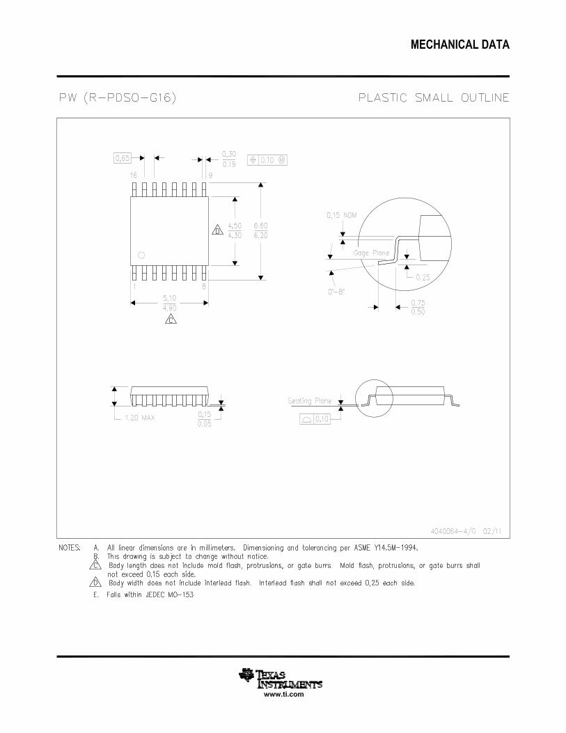
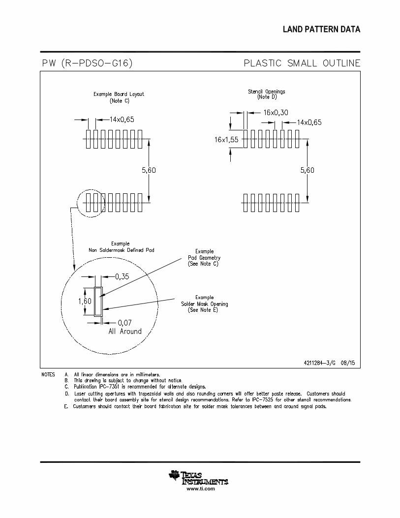
D, DB, N, NS, OR PW PACKAGE
(TOP VIEW)
Product
Folder
Sample &Buy
Technical
Documents
Tools &
Software
Support &Community
TL494SLVS074G –JANUARY 1983–REVISED JANUARY 2015
TL494 Pulse-Width-Modulation Control Circuits1 Features 3 Description
The TL494 device incorporates all the functions1• Complete PWM Power-Control Circuitry
required in the construction of a pulse-width-• Uncommitted Outputs for 200-mA Sink or modulation (PWM) control circuit on a single chip.Source Current Designed primarily for power-supply control, this
• Output Control Selects Single-Ended or device offers the flexibility to tailor the power-supplycontrol circuitry to a specific application.Push-Pull Operation
• Internal Circuitry Prohibits Double Pulse at The TL494 device contains two error amplifiers, anEither Output on-chip adjustable oscillator, a dead-time control
(DTC) comparator, a pulse-steering control flip-flop, a• Variable Dead Time Provides Control Over5-V, 5%-precision regulator, and output-controlTotal Rangecircuits.• Internal Regulator Provides a Stable 5-VThe error amplifiers exhibit a common-mode voltageReference Supply With 5% Tolerancerange from –0.3 V to VCC – 2 V. The dead-time• Circuit Architecture Allows Easy Synchronization control comparator has a fixed offset that providesapproximately 5% dead time. The on-chip oscillator2 Applications can be bypassed by terminating RT to the referenceoutput and providing a sawtooth input to CT, or it can• Desktop PCsdrive the common circuits in synchronous multiple-rail• Microwave Ovenspower supplies.
• Power Supplies: AC/DC, Isolated,The uncommitted output transistors provide eitherWith PFC, > 90 Wcommon-emitter or emitter-follower output capability.• Server PSUs The TL494 device provides for push-pull or single-
• Solar Micro-Inverters ended output operation, which can be selectedthrough the output-control function. The architecture• Washing Machines: Low-End and High-Endof this device prohibits the possibility of either output• E-Bikesbeing pulsed twice during push-pull operation.
• Power Supplies: AC/DC, Isolated,The TL494C device is characterized for operationNo PFC, < 90 Wfrom 0°C to 70°C. The TL494I device is characterized• Power: Telecom/Server AC/DC Supplies: for operation from –40°C to 85°C.Dual Controller: Analog
• Smoke Detectors Device Information(1)
PART NUMBER PACKAGE (PIN) BODY SIZE• Solar Power InvertersSOIC (16) 9.90 mm × 3.91 mm
PDIP (16) 19.30 mm × 6.35 mmTL494
SOP (16) 10.30 mm × 5.30 mm
TSSOP (16) 5.00 mm × 4.40 mm
(1) For all available packages, see the orderable addendum atthe end of the data sheet.
4 Pinout Drawing
1
An IMPORTANT NOTICE at the end of this data sheet addresses availability, warranty, changes, use in safety-critical applications,intellectual property matters and other important disclaimers. PRODUCTION DATA.
TL494SLVS074G –JANUARY 1983–REVISED JANUARY 2015 www.ti.com
Table of Contents7.13 Typical Characteristics ............................................ 71 Features .................................................................. 1
8 Parameter Measurement Information .................. 82 Applications ........................................................... 19 Detailed Description ............................................ 103 Description ............................................................. 1
9.1 Overview ................................................................. 104 Pinout Drawing....................................................... 19.2 Functional Block Diagram ....................................... 105 Revision History..................................................... 29.3 Feature Description................................................. 106 Pin Configuration and Functions ......................... 39.4 Device Functional Modes........................................ 127 Specifications......................................................... 4
10 Application and Implementation........................ 137.1 Absolute Maximum Ratings ...................................... 410.1 Application Information.......................................... 137.2 ESD Ratings.............................................................. 410.2 Typical Application ............................................... 137.3 Recommended Operating Conditions....................... 4
11 Power Supply Recommendations ..................... 207.4 Thermal Information .................................................. 412 Layout................................................................... 207.5 Electrical Characteristics, Reference Section ........... 5
12.1 Layout Guidelines ................................................. 207.6 Electrical Characteristics, Oscillator Section............. 512.2 Layout Example .................................................... 217.7 Electrical Characteristics, Error-Amplifier Section .... 5
13 Device and Documentation Support ................. 217.8 Electrical Characteristics, Output Section................. 613.1 Trademarks ........................................................... 217.9 Electrical Characteristics, Dead-Time Control
Section ....................................................................... 6 13.2 Electrostatic Discharge Caution............................ 217.10 Electrical Characteristics, PWM Comparator 13.3 Glossary ................................................................ 21
Section ....................................................................... 6 14 Mechanical, Packaging, and Orderable7.11 Electrical Characteristics, Total Device................... 6 Information ........................................................... 217.12 Switching Characteristics ........................................ 6
5 Revision History
Changes from Revision F (January 2014) to Revision G Page
• Added Applications, Device Information table, Pin Functions table, ESD Ratings table, Thermal Information table, ,Feature Description section, Device Functional Modes, Application and Implementation section, Power SupplyRecommendations section, Layout section, Device and Documentation Support section, and Mechanical,Packaging, and Orderable Information section. ..................................................................................................................... 1
Changes from Revision E (February 2005) to Revision F Page
• Updated document to new TI data sheet format - no specification changes. ........................................................................ 1• Removed Ordering Information table. .................................................................................................................................... 1• Added ESD warning. ............................................................................................................................................................ 21
2 Submit Documentation Feedback Copyright © 1983–2015, Texas Instruments Incorporated
Product Folder Links: TL494
1
2
3
4
5
6
7
8
16
15
14
13
12
11
10
9
1IN+
1IN−
FEEDBACK
DTC
CT
RT
GND
C1
2IN+
2IN−
REF
OUTPUT CTRL
VCC
C2
E2
E1
D, DB, N, NS, OR PW PACKAGE
(TOP VIEW)
TL494www.ti.com SLVS074G –JANUARY 1983–REVISED JANUARY 2015
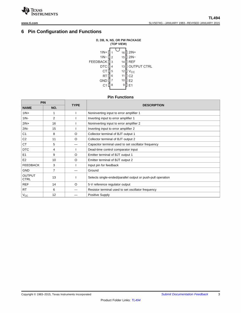
6 Pin Configuration and Functions
Pin FunctionsPIN
TYPE DESCRIPTIONNAME NO.1IN+ 1 I Noninverting input to error amplifier 11IN- 2 I Inverting input to error amplifier 12IN+ 16 I Noninverting input to error amplifier 22IN- 15 I Inverting input to error amplifier 2C1 8 O Collector terminal of BJT output 1C2 11 O Collector terminal of BJT output 2CT 5 — Capacitor terminal used to set oscillator frequencyDTC 4 I Dead-time control comparator inputE1 9 O Emitter terminal of BJT output 1E2 10 O Emitter terminal of BJT output 2FEEDBACK 3 I Input pin for feedbackGND 7 — GroundOUTPUT 13 I Selects single-ended/parallel output or push-pull operationCTRLREF 14 O 5-V reference regulator outputRT 6 — Resistor terminal used to set oscillator frequencyVCC 12 — Positive Supply
Copyright © 1983–2015, Texas Instruments Incorporated Submit Documentation Feedback 3
Product Folder Links: TL494
TL494SLVS074G –JANUARY 1983–REVISED JANUARY 2015 www.ti.com
7 Specifications
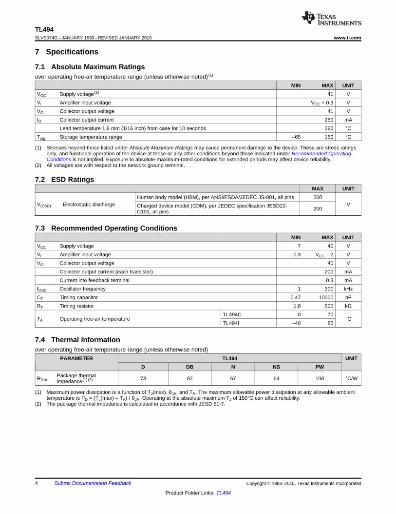
7.1 Absolute Maximum Ratingsover operating free-air temperature range (unless otherwise noted) (1)
MIN MAX UNITVCC Supply voltage (2) 41 VVI Amplifier input voltage VCC + 0.3 VVO Collector output voltage 41 VIO Collector output current 250 mA
Lead temperature 1,6 mm (1/16 inch) from case for 10 seconds 260 °CTstg Storage temperature range –65 150 °C
(1) Stresses beyond those listed under Absolute Maximum Ratings may cause permanent damage to the device. These are stress ratingsonly, and functional operation of the device at these or any other conditions beyond those indicated under Recommended OperatingConditions is not implied. Exposure to absolute-maximum-rated conditions for extended periods may affect device reliability.
(2) All voltages are with respect to the network ground terminal.
7.2 ESD RatingsMAX UNIT
Human body model (HBM), per ANSI/ESDA/JEDEC JS-001, all pins 500V(ESD) Electrostatic discharge VCharged device model (CDM), per JEDEC specification JESD22- 200C101, all pins
7.3 Recommended Operating ConditionsMIN MAX UNIT
VCC Supply voltage 7 40 VVI Amplifier input voltage –0.3 VCC – 2 VVO Collector output voltage 40 V
Collector output current (each transistor) 200 mACurrent into feedback terminal 0.3 mA
fOSC Oscillator frequency 1 300 kHzCT Timing capacitor 0.47 10000 nFRT Timing resistor 1.8 500 kΩ
TL494C 0 70TA Operating free-air temperature °C
TL494I –40 85
7.4 Thermal Informationover operating free-air temperature range (unless otherwise noted)
PARAMETER TL494 UNITD DB N NS PW
Package thermalRθJA 73 82 67 64 108 °C/Wimpedance (1) (2)
(1) Maximum power dissipation is a function of TJ(max), θJA, and TA. The maximum allowable power dissipation at any allowable ambienttemperature is PD = (TJ(max) – TA) / θJA. Operating at the absolute maximum TJ of 150°C can affect reliability.
(2) The package thermal impedance is calculated in accordance with JESD 51-7.
4 Submit Documentation Feedback Copyright © 1983–2015, Texas Instruments Incorporated
Product Folder Links: TL494
( )N
2
n
n 1
x X
N 1
=
-
s =-
å
TL494www.ti.com SLVS074G –JANUARY 1983–REVISED JANUARY 2015
7.5 Electrical Characteristics, Reference Sectionover recommended operating free-air temperature range, VCC = 15 V, f = 10 kHz (unless otherwise noted)
TL494C, TL494IPARAMETER TEST CONDITIONS (1) UNIT
MIN TYP (2) MAXOutput voltage (REF) IO = 1 mA 4.75 5 5.25 VInput regulation VCC = 7 V to 40 V 2 25 mVOutput regulation IO = 1 mA to 10 mA 1 15 mVOutput voltage change with temperature ΔTA = MIN to MAX 2 10 mV/VShort-circuit output current (3) REF = 0 V 25 mA
(1) For conditions shown as MIN or MAX, use the appropriate value specified under recommended operating conditions.(2) All typical values, except for parameter changes with temperature, are at TA = 25°C.(3) Duration of short circuit should not exceed one second.
7.6 Electrical Characteristics, Oscillator SectionCT = 0.01 μF, RT = 12 kΩ (see Figure 5)
TL494C, TL494IPARAMETER TEST CONDITIONS (1) UNIT
MIN TYP (2) MAXFrequency 10 kHzStandard deviation of frequency (3) All values of VCC, CT, RT, and TA constant 100 Hz/kHzFrequency change with voltage VCC = 7 V to 40 V, TA = 25°C 1 Hz/kHzFrequency change with temperature (4) ΔTA = MIN to MAX 10 Hz/kHz
(1) For conditions shown as MIN or MAX, use the appropriate value specified under recommended operating conditions.(2) All typical values, except for parameter changes with temperature, are at TA = 25°C.(3) Standard deviation is a measure of the statistical distribution about the mean as derived from the formula:
(4) Temperature coefficient of timing capacitor and timing resistor are not taken into account.
7.7 Electrical Characteristics, Error-Amplifier SectionSee Figure 6
TL494C, TL494IPARAMETER TEST CONDITIONS UNIT
MIN TYP (1) MAXInput offset voltage VO (FEEDBACK) = 2.5 V 2 10 mVInput offset current VO (FEEDBACK) = 2.5 V 25 250 nAInput bias current VO (FEEDBACK) = 2.5 V 0.2 1 μACommon-mode input voltage range VCC = 7 V to 40 V –0.3 to VCC – 2 VOpen-loop voltage amplification ΔVO = 3 V, VO = 0.5 V to 3.5 V, RL = 2 kΩ 70 95 dBUnity-gain bandwidth VO = 0.5 V to 3.5 V, RL = 2 kΩ 800 kHzCommon-mode rejection ratio ΔVO = 40 V, TA = 25°C 65 80 dBOutput sink current (FEEDBACK) VID = –15 mV to –5 V, V (FEEDBACK) = 0.7 V 0.3 0.7 mAOutput source current (FEEDBACK) VID = 15 mV to 5 V, V (FEEDBACK) = 3.5 V –2 mA
(1) All typical values, except for parameter changes with temperature, are at TA = 25°C.
Copyright © 1983–2015, Texas Instruments Incorporated Submit Documentation Feedback 5
Product Folder Links: TL494
TL494SLVS074G –JANUARY 1983–REVISED JANUARY 2015 www.ti.com
7.8 Electrical Characteristics, Output SectionPARAMETER TEST CONDITIONS MIN TYP (1) MAX UNIT
Collector off-state current VCE = 40 V, VCC = 40 V 2 100 μAEmitter off-state current VCC = VC = 40 V, VE = 0 –100 μA
Common emitter VE = 0, IC = 200 mA 1.1 1.3Collector-emitter saturation voltage V
Emitter follower VO(C1 or C2) = 15 V, IE = –200 mA 1.5 2.5Output control input current VI = Vref 3.5 mA
(1) All typical values, except for temperature coefficient, are at TA = 25°C.
7.9 Electrical Characteristics, Dead-Time Control SectionSee Figure 5
PARAMETER TEST CONDITIONS MIN TYP (1) MAX UNITInput bias current (DEAD-TIME CTRL) VI = 0 to 5.25 V –2 –10 μA
VI (DEAD-TIME CTRL) = 0, CT = 0.01 μF,Maximum duty cycle, each output 45% —RT = 12 kΩZero duty cycle 3 3.3
Input threshold voltage (DEAD-TIME CTRL) VMaximum duty cycle 0
(1) All typical values, except for temperature coefficient, are at TA = 25°C.
7.10 Electrical Characteristics, PWM Comparator SectionSee Figure 5
PARAMETER TEST CONDITIONS MIN TYP (1) MAX UNITInput threshold voltage (FEEDBACK) Zero duty cyle 4 4.5 VInput sink current (FEEDBACK) V (FEEDBACK) = 0.7 V 0.3 0.7 mA
(1) All typical values, except for temperature coefficient, are at TA = 25°C.
7.11 Electrical Characteristics, Total DevicePARAMETER TEST CONDITIONS MIN TYP (1) MAX UNIT
VCC = 15 V 6 10RT = Vref,Standby supply current mAAll other inputs and outputs open VCC = 40 V 9 15Average supply current VI (DEAD-TIME CTRL) = 2 V, See Figure 5 7.5 mA
(1) All typical values, except for temperature coefficient, are at TA = 25°C.
7.12 Switching CharacteristicsTA = 25°C
PARAMETER TEST CONDITIONS MIN TYP (1) MAX UNITRise time 100 200 ns
Common-emitter configuration, See Figure 7Fall time 25 100 nsRise time 100 200 ns
Emitter-follower configuration, See Figure 8Fall time 40 100 ns
(1) All typical values, except for temperature coefficient, are at TA = 25°C.
6 Submit Documentation Feedback Copyright © 1983–2015, Texas Instruments Incorporated
Product Folder Links: TL494
4
3
2
1
00 10 20
VI − Input Voltage − (mV)
VO
−O
utp
ut
Vo
ltag
e−
(V)
80
60
40
20
00 10k 1M
f − Frequency − (Hz)
100k
Gain
−(d
B)
Df = 1%(1)
40
10
100
1 k 4 k 10 k 40 k 100 k 400 k 1 M
f−
Oscilla
tor
Fre
qu
en
cy a
nd
Fre
qu
en
cy V
ari
ati
on
−H
z
400
1 k
4 k
10 k
40 k
100 k
RT − Timing Resistance − Ω
0.1 Fµ
−2%
−1%
0%0.01 Fµ
0.001 Fµ
VCC = 15 V
TA = 25 C°
CT = 1 Fµ
10
0
100
20
1 10 100 1 M
A−
Am
plifi
er
Vo
ltag
eA
mp
lifi
cati
on
−d
B
30
f − Frequency − Hz
1 k
VCC = 15 V
ΔVO = 3 V
TA = 25 C°
10 k
40
50
60
70
80
90
100 k
TL494www.ti.com SLVS074G –JANUARY 1983–REVISED JANUARY 2015
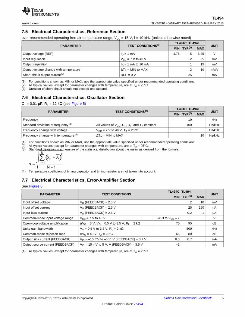
7.13 Typical Characteristics
xxxFrequency variation (Δf) is the change in oscillator frequency xxxthat occurs over the full temperature range. Figure 2. Amplifier Voltage Amplification
Figure 1. Oscillator Frequency and Frequency Variation vsvs Frequency
Timing Resistance
Figure 3. Error Amplifier Transfer CharacteristicsFigure 4. Error Amplifier Bode Plot
Copyright © 1983–2015, Texas Instruments Incorporated Submit Documentation Feedback 7
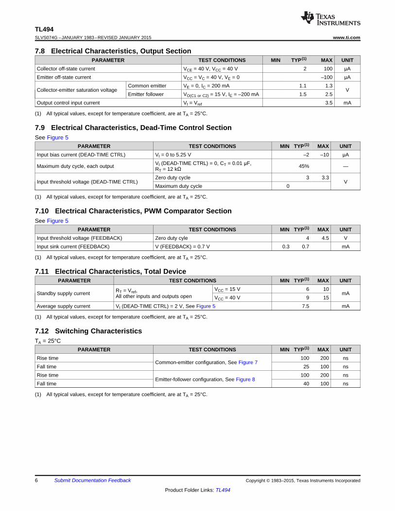
Product Folder Links: TL494
Test
Inputs
DTC
FEEDBACK
RT
CT
GND50 kW
12 kW
0.01 mF
VCC
REFOUTPUT
CTRL
E2
C2
E1
C1 Output 1
Output 2
150 W
2 W
150 W
2 W
VCC = 15 V
TEST CIRCUIT
1IN+
VCC
VCC
0 V
0 V
Voltage
at C1
Voltage
at C2
Voltage
at CT
DTC
FEEDBACK
0 V
0.7 V
0%MAX 0%
Threshold Voltage
Threshold Voltage
VOLTAGE WAVEFORMS
Duty Cycle
Error
Amplifiers
7
14
12
8
9
11
10
4
3
6
5
1
2
16
15
13
1IN−
2IN−
2IN+
TL494SLVS074G –JANUARY 1983–REVISED JANUARY 2015 www.ti.com
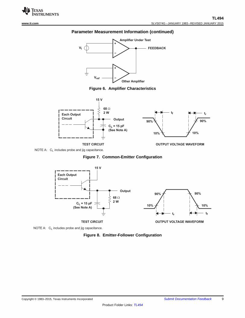
8 Parameter Measurement Information
Figure 5. Operational Test Circuit and Waveforms
8 Submit Documentation Feedback Copyright © 1983–2015, Texas Instruments Incorporated
Product Folder Links: TL494
Output
Each Output
Circuit
68 W
2 W
15 V
CL = 15 pF
(See Note A)
90%
10%
90%
10%
tftr
TEST CIRCUIT OUTPUT VOLTAGE WAVEFORM
NOTE A: CL includes probe and jig capacitance.
Output
Each Output
Circuit
68 W
2 W
15 V
CL = 15 pF
(See Note A)
90%
10%
90%
10%
tf tr
TEST CIRCUIT OUTPUT VOLTAGE WAVEFORM
NOTE A: CL includes probe and jig capacitance.
+
−
+
−
VI
Vref
FEEDBACK
Amplifier Under Test
Other Amplifier
TL494www.ti.com SLVS074G –JANUARY 1983–REVISED JANUARY 2015
Parameter Measurement Information (continued)
Figure 6. Amplifier Characteristics
Figure 7. Common-Emitter Configuration
Figure 8. Emitter-Follower Configuration
Copyright © 1983–2015, Texas Instruments Incorporated Submit Documentation Feedback 9
Product Folder Links: TL494
GND
VCC
Reference
Regulator
C1
Pulse-Steering
Flip-Flop
C1
1D
DTC
CT
RT
PWM
Comparator
+
−
Error Amplifier 1
≈0.1 V
Dead-Time Control
Comparator
Oscillator
OUTPUT CTRL
(see Function Table)
0.7 mA
E1
C2
E2
+
−
Error Amplifier 2
1IN+
1IN−
2IN+
2IN−
FEEDBACK
REF
6
5
4
1
2
16
15
3
13
8
9
11
10
12
14
7
Q1
Q2≈0.7 V
TL494SLVS074G –JANUARY 1983–REVISED JANUARY 2015 www.ti.com
9 Detailed Description
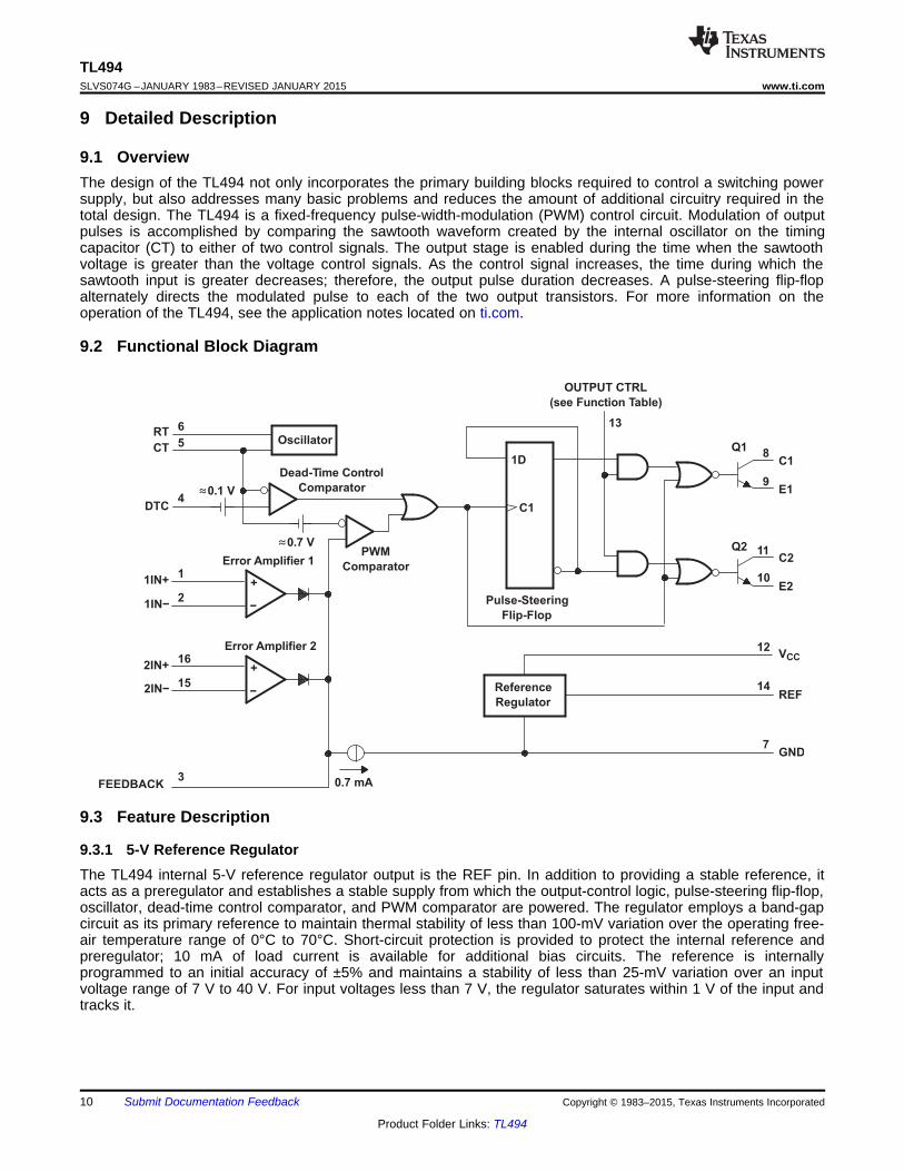
9.1 OverviewThe design of the TL494 not only incorporates the primary building blocks required to control a switching powersupply, but also addresses many basic problems and reduces the amount of additional circuitry required in thetotal design. The TL494 is a fixed-frequency pulse-width-modulation (PWM) control circuit. Modulation of outputpulses is accomplished by comparing the sawtooth waveform created by the internal oscillator on the timingcapacitor (CT) to either of two control signals. The output stage is enabled during the time when the sawtoothvoltage is greater than the voltage control signals. As the control signal increases, the time during which thesawtooth input is greater decreases; therefore, the output pulse duration decreases. A pulse-steering flip-flopalternately directs the modulated pulse to each of the two output transistors. For more information on theoperation of the TL494, see the application notes located on ti.com.
9.2 Functional Block Diagram
9.3 Feature Description
9.3.1 5-V Reference RegulatorThe TL494 internal 5-V reference regulator output is the REF pin. In addition to providing a stable reference, itacts as a preregulator and establishes a stable supply from which the output-control logic, pulse-steering flip-flop,oscillator, dead-time control comparator, and PWM comparator are powered. The regulator employs a band-gapcircuit as its primary reference to maintain thermal stability of less than 100-mV variation over the operating free-air temperature range of 0°C to 70°C. Short-circuit protection is provided to protect the internal reference andpreregulator; 10 mA of load current is available for additional bias circuits. The reference is internallyprogrammed to an initial accuracy of ±5% and maintains a stability of less than 25-mV variation over an inputvoltage range of 7 V to 40 V. For input voltages less than 7 V, the regulator saturates within 1 V of the input andtracks it.
10 Submit Documentation Feedback Copyright © 1983–2015, Texas Instruments Incorporated
Product Folder Links: TL494
T T
1f
2R C=
´
T T
1f
R C=
´
OSC
T T
1f
R C=
´
T
CHARGE
3 V CT
I
´
=
CHARGE
T
3 VI
R=
TL494www.ti.com SLVS074G –JANUARY 1983–REVISED JANUARY 2015
Feature Description (continued)9.3.2 OscillatorThe oscillator provides a positive sawtooth waveform to the dead-time and PWM comparators for comparison tothe various control signals.
The frequency of the oscillator is programmed by selecting timing components RT and CT. The oscillator chargesthe external timing capacitor, CT, with a constant current, the value of which is determined by the external timingresistor, RT. This produces a linear-ramp voltage waveform. When the voltage across CT reaches 3 V, theoscillator circuit discharges it, and the charging cycle is reinitiated. The charging current is determined by theformula:
(1)
The period of the sawtooth waveform is:
(2)
The frequency of the oscillator becomes:
(3)
However, the oscillator frequency is equal to the output frequency only for single-ended applications. For push-pull applications, the output frequency is one-half the oscillator frequency.
Single-ended applications:
(4)
Push-pull applications:
(5)
9.3.3 Dead-time ControlThe dead-time control input provides control of the minimum dead time (off time). The output of the comparatorinhibits switching transistors Q1 and Q2 when the voltage at the input is greater than the ramp voltage of theoscillator. An internal offset of 110 mV ensures a minimum dead time of ∼3% with the dead-time control inputgrounded. Applying a voltage to the dead-time control input can impose additional dead time. This provides alinear control of the dead time from its minimum of 3% to 100% as the input voltage is varied from 0 V to 3.3 V,respectively. With full-range control, the output can be controlled from external sources without disrupting theerror amplifiers. The dead-time control input is a relatively high-impedance input (II < 10 μA) and should be usedwhere additional control of the output duty cycle is required. However, for proper control, the input must beterminated. An open circuit is an undefined condition.
9.3.4 ComparatorThe comparator is biased from the 5-V reference regulator. This provides isolation from the input supply forimproved stability. The input of the comparator does not exhibit hysteresis, so protection against false triggeringnear the threshold must be provided. The comparator has a response time of 400 ns from either of the control-signal inputs to the output transistors, with only 100 mV of overdrive. This ensures positive control of the outputwithin one-half cycle for operation within the recommended 300-kHz range.
Copyright © 1983–2015, Texas Instruments Incorporated Submit Documentation Feedback 11
Product Folder Links: TL494
TL494SLVS074G –JANUARY 1983–REVISED JANUARY 2015 www.ti.com
Feature Description (continued)9.3.5 Pulse-Width Modulation (PWM)The comparator also provides modulation control of the output pulse width. For this, the ramp voltage acrosstiming capacitor CT is compared to the control signal present at the output of the error amplifiers. The timingcapacitor input incorporates a series diode that is omitted from the control signal input. This requires the controlsignal (error amplifier output) to be ∼0.7 V greater than the voltage across CT to inhibit the output logic, andensures maximum duty cycle operation without requiring the control voltage to sink to a true ground potential.The output pulse width varies from 97% of the period to 0 as the voltage present at the error amplifier outputvaries from 0.5 V to 3.5 V, respectively.
9.3.6 Error AmplifiersBoth high-gain error amplifiers receive their bias from the VI supply rail. This permits a common-mode inputvoltage range from –0.3 V to 2 V less than VI. Both amplifiers behave characteristically of a single-ended single-supply amplifier, in that each output is active high only. This allows each amplifier to pull up independently for adecreasing output pulse-width demand. With both outputs ORed together at the inverting input node of the PWMcomparator, the amplifier demanding the minimum pulse out dominates. The amplifier outputs are biased low bya current sink to provide maximum pulse width out when both amplifiers are biased off.
9.3.7 Output-Control InputThe output-control input determines whether the output transistors operate in parallel or push-pull. This input isthe supply source for the pulse-steering flip-flop. The output-control input is asynchronous and has direct controlover the output, independent of the oscillator or pulse-steering flip-flop. The input condition is intended to be afixed condition that is defined by the application. For parallel operation, the output-control input must begrounded. This disables the pulse-steering flip-flop and inhibits its outputs. In this mode, the pulses seen at theoutput of the dead-time control/PWM comparator are transmitted by both output transistors in parallel. For push-pull operation, the output-control input must be connected to the internal 5-V reference regulator. Under thiscondition, each of the output transistors is enabled, alternately, by the pulse-steering flip-flop.
9.3.8 Output TransistorsTwo output transistors are available on the TL494. Both transistors are configured as open collector/openemitter, and each is capable of sinking or sourcing up to 200 mA. The transistors have a saturation voltage ofless than 1.3 V in the common-emitter configuration and less than 2.5 V in the emitter-follower configuration. Theoutputs are protected against excessive power dissipation to prevent damage, but do not employ sufficientcurrent limiting to allow them to be operated as current-source outputs.
9.4 Device Functional ModesWhen the OUTPUT CTRL pin is tied to ground, the TL494 is operating in single-ended or parallel mode. Whenthe OUTPUT CTRL pin is tied to VREF, the TL494 is operating in normal push-pull operation.
12 Submit Documentation Feedback Copyright © 1983–2015, Texas Instruments Incorporated
Product Folder Links: TL494
VREF
R1
1 kW
Load
Control
Osc
NTE331 140 mH
VO
NTE6013
NTE153
TL494
R2
4 kW
5-V
REF
R11
100 W
R12
30 W
R10
270 W
1 2 3 4 6 7 8
910111213141516
RF
51 kWRT
50 kW
R5
510 W
R7
9.1 kW
R3
5.1 kW
R4
5.1 kW
R6
1 kWC2
2.5 mF
5-V
REF5-V
REF
R13
0.1 W
CT
0.001 Fm
5
R8
5.1 k
R9
5.1 k
Q2
Q1
+ −
+ −
32-V
Input
TL494www.ti.com SLVS074G –JANUARY 1983–REVISED JANUARY 2015
10 Application and Implementation
NOTEInformation in the following applications sections is not part of the TI componentspecification, and TI does not warrant its accuracy or completeness. TI’s customers areresponsible for determining suitability of components for their purposes. Customers shouldvalidate and test their design implementation to confirm system functionality.
10.1 Application InformationThe following design example uses the TL494 to create a 5-V/10-A power supply. This application was takenfrom application note SLVA001.
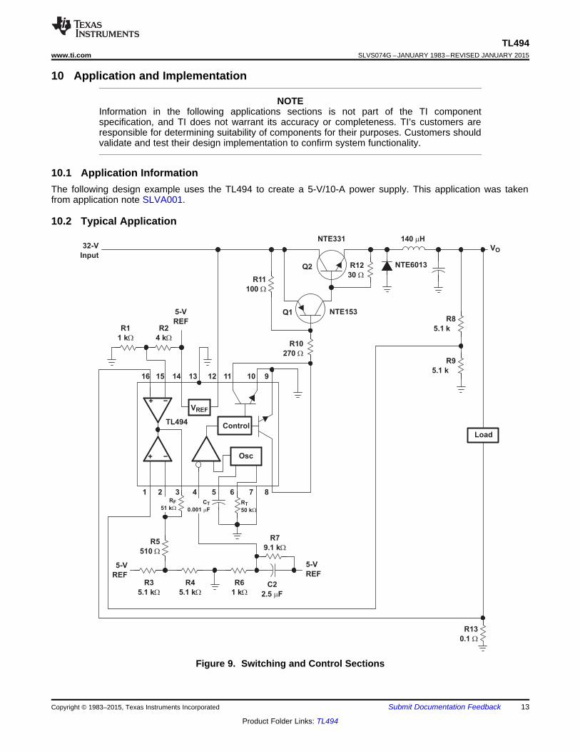
10.2 Typical Application
Figure 9. Switching and Control Sections
Copyright © 1983–2015, Texas Instruments Incorporated Submit Documentation Feedback 13
Product Folder Links: TL494
RT1
fOSC CT
1(20 103) (0.001 106)
50 k
OSC
T T
1f
R C=
´
ORECTIFIER(AVG) O
I
V 5 VI I 10 A 1.6 A
V 32V» ´ » ´ =
RECTIFIER SECONDARYV V 2 24 V 2 34 V= ´ = ´ =
20,000 μF
BridgeRectifiers3 A/50 V
20,000 μF
0.3 W
120 V24 V3 A
+32 V
+ +
TL494SLVS074G –JANUARY 1983–REVISED JANUARY 2015 www.ti.com
Typical Application (continued)10.2.1 Design Requirements• VI = 32 V• VO = 5 V• IO = 10 A• fOSC = 20-kHz switching frequency• VR = 20-mV peak-to-peak (VRIPPLE)• ΔIL = 1.5-A inductor current change
10.2.2 Detailed Design Procedure
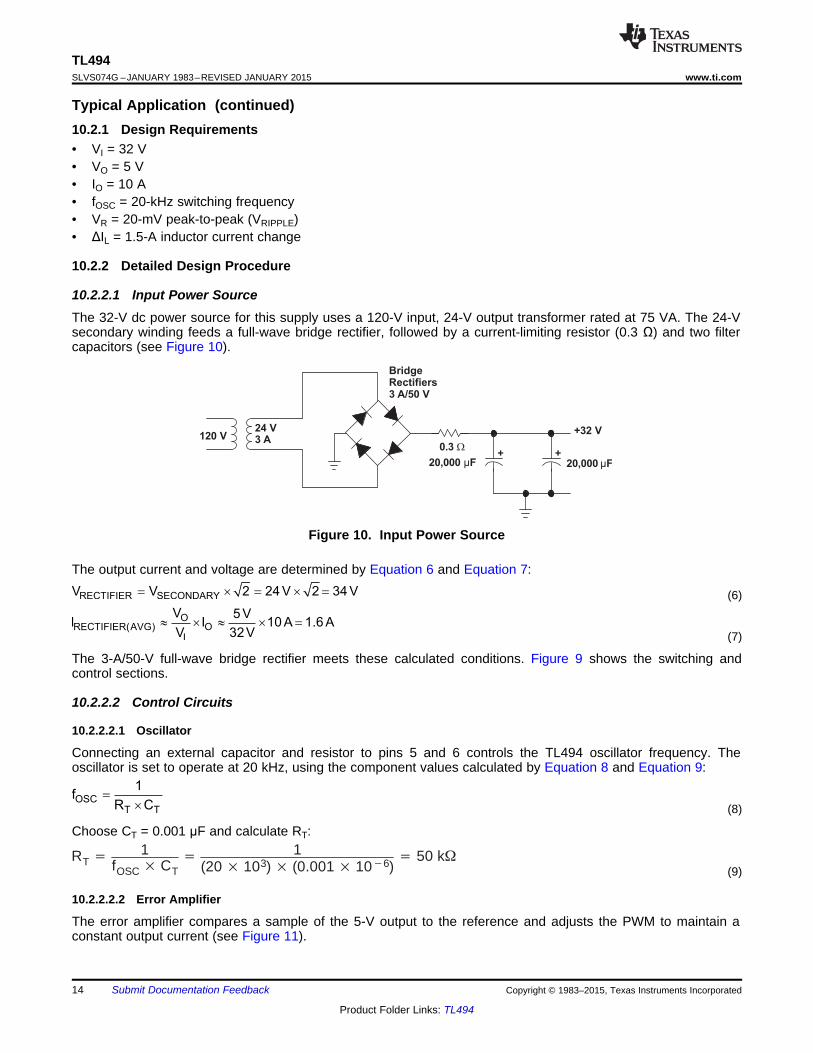
10.2.2.1 Input Power SourceThe 32-V dc power source for this supply uses a 120-V input, 24-V output transformer rated at 75 VA. The 24-Vsecondary winding feeds a full-wave bridge rectifier, followed by a current-limiting resistor (0.3 Ω) and two filtercapacitors (see Figure 10).
Figure 10. Input Power Source
The output current and voltage are determined by Equation 6 and Equation 7:
(6)
(7)
The 3-A/50-V full-wave bridge rectifier meets these calculated conditions. Figure 9 shows the switching andcontrol sections.
10.2.2.2 Control Circuits
10.2.2.2.1 Oscillator
Connecting an external capacitor and resistor to pins 5 and 6 controls the TL494 oscillator frequency. Theoscillator is set to operate at 20 kHz, using the component values calculated by Equation 8 and Equation 9:
(8)
Choose CT = 0.001 μF and calculate RT:
(9)
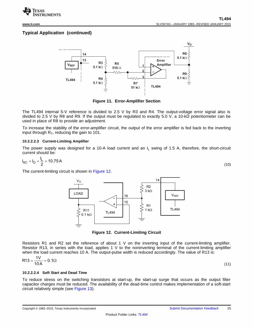
10.2.2.2.2 Error Amplifier
The error amplifier compares a sample of the 5-V output to the reference and adjusts the PWM to maintain aconstant output current (see Figure 11).
14 Submit Documentation Feedback Copyright © 1983–2015, Texas Instruments Incorporated
Product Folder Links: TL494
1VR13 0.1
10 A= = W
+
LOAD
VO
TL494
R1
1 kW
R2
3 kW
16
15
VREF
TL494
14
R11
0.1 kW
LSC O
II I 10.75 A
2= + =
R8
5.1 kW
VO
VREF +
−
1
14
13 Error
Amplifier
2
3
TL494
R9
5.1 kW
R5
510 W
R7
51 kW
R3
5.1 kW
R4
5.1 kW
TL494
TL494www.ti.com SLVS074G –JANUARY 1983–REVISED JANUARY 2015
Typical Application (continued)
Figure 11. Error-Amplifier Section
The TL494 internal 5-V reference is divided to 2.5 V by R3 and R4. The output-voltage error signal also isdivided to 2.5 V by R8 and R9. If the output must be regulated to exactly 5.0 V, a 10-kΩ potentiometer can beused in place of R8 to provide an adjustment.
To increase the stability of the error-amplifier circuit, the output of the error amplifier is fed back to the invertinginput through RT, reducing the gain to 101.
10.2.2.2.3 Current-Limiting Amplifier
The power supply was designed for a 10-A load current and an IL swing of 1.5 A, therefore, the short-circuitcurrent should be:
(10)
The current-limiting circuit is shown in Figure 12.
Figure 12. Current-Limiting Circuit
Resistors R1 and R2 set the reference of about 1 V on the inverting input of the current-limiting amplifier.Resistor R13, in series with the load, applies 1 V to the noninverting terminal of the current-limiting amplifierwhen the load current reaches 10 A. The output-pulse width is reduced accordingly. The value of R13 is:
(11)
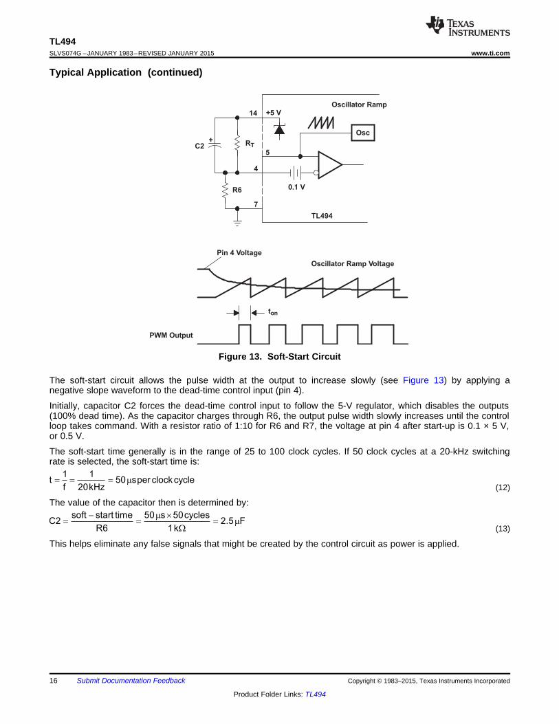
10.2.2.2.4 Soft Start and Dead Time
To reduce stress on the switching transistors at start-up, the start-up surge that occurs as the output filtercapacitor charges must be reduced. The availability of the dead-time control makes implementation of a soft-startcircuit relatively simple (see Figure 13).
Copyright © 1983–2015, Texas Instruments Incorporated Submit Documentation Feedback 15
Product Folder Links: TL494
soft start time 50 s 50cyclesC2 2.5 F
R6 1k
- m ´= = = m
W
1 1t 50 sper clock cycle
f 20kHz= = = m
TL494
Pin 4 Voltage
PWM Output
Oscillator Ramp Voltage
ton
RTC2
+5 V
0.1 V
Osc
R6
14
5
4
7
Oscillator Ramp
+
TL494SLVS074G –JANUARY 1983–REVISED JANUARY 2015 www.ti.com
Typical Application (continued)
Figure 13. Soft-Start Circuit
The soft-start circuit allows the pulse width at the output to increase slowly (see Figure 13) by applying anegative slope waveform to the dead-time control input (pin 4).
Initially, capacitor C2 forces the dead-time control input to follow the 5-V regulator, which disables the outputs(100% dead time). As the capacitor charges through R6, the output pulse width slowly increases until the controlloop takes command. With a resistor ratio of 1:10 for R6 and R7, the voltage at pin 4 after start-up is 0.1 × 5 V,or 0.5 V.
The soft-start time generally is in the range of 25 to 100 clock cycles. If 50 clock cycles at a 20-kHz switchingrate is selected, the soft-start time is:
(12)
The value of the capacitor then is determined by:
(13)
This helps eliminate any false signals that might be created by the control circuit as power is applied.
16 Submit Documentation Feedback Copyright © 1983–2015, Texas Instruments Incorporated
Product Folder Links: TL494
L
3O
I 1.5 AC3 94 F
8f V 8 20 10 0.1 V
D= = = m
D ´ ´ ´
O(ripple)
L
V VESR(max) 0.067
I 1.5 A
D= = » W
D
R1C1
D1
S1
L
VOVI
TL494www.ti.com SLVS074G –JANUARY 1983–REVISED JANUARY 2015
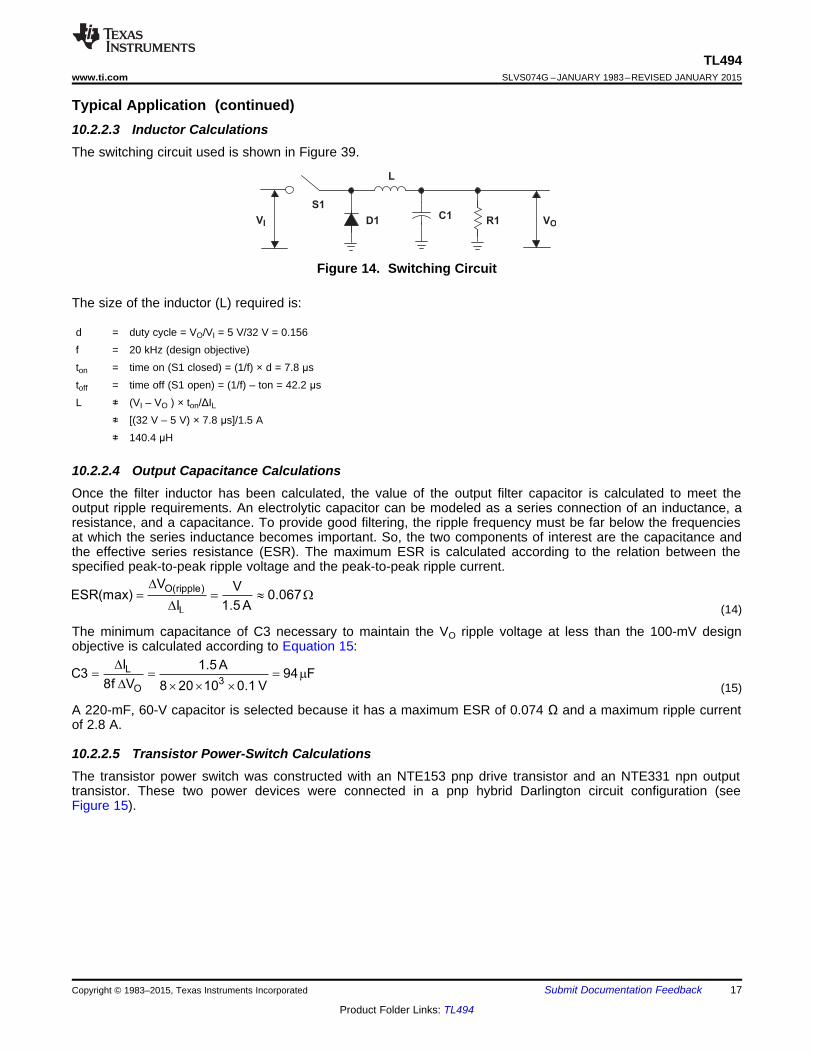
Typical Application (continued)10.2.2.3 Inductor CalculationsThe switching circuit used is shown in Figure 39.
Figure 14. Switching Circuit
The size of the inductor (L) required is:
d = duty cycle = VO/VI = 5 V/32 V = 0.156f = 20 kHz (design objective)ton = time on (S1 closed) = (1/f) × d = 7.8 μstoff = time off (S1 open) = (1/f) – ton = 42.2 μsL ≉ (VI – VO ) × ton/ΔIL
≉ [(32 V – 5 V) × 7.8 μs]/1.5 A≉ 140.4 μH
10.2.2.4 Output Capacitance CalculationsOnce the filter inductor has been calculated, the value of the output filter capacitor is calculated to meet theoutput ripple requirements. An electrolytic capacitor can be modeled as a series connection of an inductance, aresistance, and a capacitance. To provide good filtering, the ripple frequency must be far below the frequenciesat which the series inductance becomes important. So, the two components of interest are the capacitance andthe effective series resistance (ESR). The maximum ESR is calculated according to the relation between thespecified peak-to-peak ripple voltage and the peak-to-peak ripple current.
(14)
The minimum capacitance of C3 necessary to maintain the VO ripple voltage at less than the 100-mV designobjective is calculated according to Equation 15:
(15)
A 220-mF, 60-V capacitor is selected because it has a maximum ESR of 0.074 Ω and a maximum ripple currentof 2.8 A.
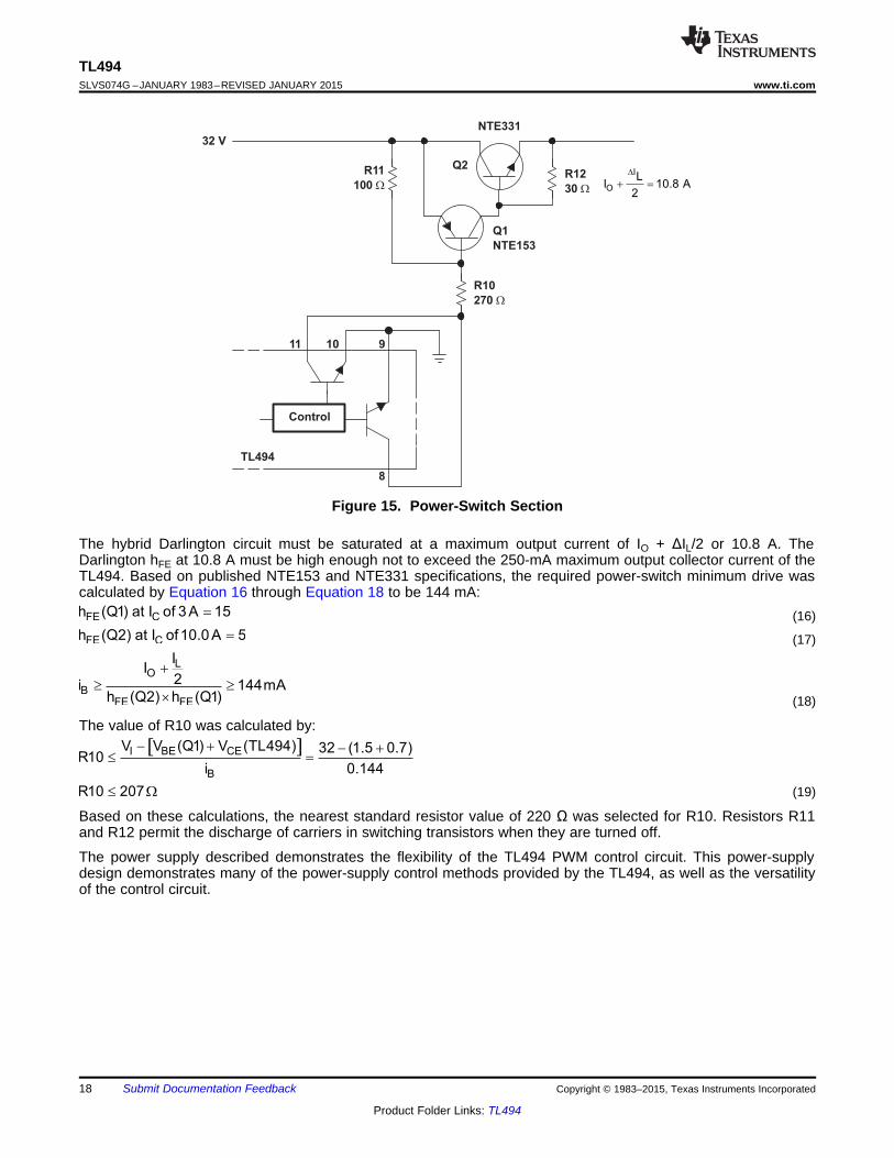
10.2.2.5 Transistor Power-Switch CalculationsThe transistor power switch was constructed with an NTE153 pnp drive transistor and an NTE331 npn outputtransistor. These two power devices were connected in a pnp hybrid Darlington circuit configuration (seeFigure 15).
Copyright © 1983–2015, Texas Instruments Incorporated Submit Documentation Feedback 17
Product Folder Links: TL494
[ ]I BE CE
B
V V (Q1) V (TL494) 32 (1.5 0.7)R10
i 0.144
R10 207
- + - +£ =
£ W
LO
BFE FE
II
2i 144mAh (Q2) h (Q1)
+
³ ³
´
FE Ch (Q2) at I of10.0 A 5=
FE Ch (Q1) at I of 3 A 15=
NTE331
TL494
Control
Q2
11 10 9
Q1
NTE153
32 V
8
R10
270 W
R12
30 W
R11
100 W
I
O
LI 10.8 A
2
D
+ =
TL494SLVS074G –JANUARY 1983–REVISED JANUARY 2015 www.ti.com
Figure 15. Power-Switch Section
The hybrid Darlington circuit must be saturated at a maximum output current of IO + ΔIL/2 or 10.8 A. TheDarlington hFE at 10.8 A must be high enough not to exceed the 250-mA maximum output collector current of theTL494. Based on published NTE153 and NTE331 specifications, the required power-switch minimum drive wascalculated by Equation 16 through Equation 18 to be 144 mA:
(16)
(17)
(18)
The value of R10 was calculated by:
(19)
Based on these calculations, the nearest standard resistor value of 220 Ω was selected for R10. Resistors R11and R12 permit the discharge of carriers in switching transistors when they are turned off.
The power supply described demonstrates the flexibility of the TL494 PWM control circuit. This power-supplydesign demonstrates many of the power-supply control methods provided by the TL494, as well as the versatilityof the control circuit.
18 Submit Documentation Feedback Copyright © 1983–2015, Texas Instruments Incorporated
Product Folder Links: TL494
5
4
3
2
1
00 1 2 3 4 5 6 7
VI − Input Voltage − (V)
6
VR
EF
−R
efe
ren
ce V
olt
ag
e−
(V)
TL494www.ti.com SLVS074G –JANUARY 1983–REVISED JANUARY 2015
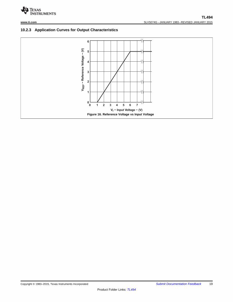
10.2.3 Application Curves for Output Characteristics
Figure 16. Reference Voltage vs Input Voltage
Copyright © 1983–2015, Texas Instruments Incorporated Submit Documentation Feedback 19
Product Folder Links: TL494
TL494SLVS074G –JANUARY 1983–REVISED JANUARY 2015 www.ti.com
11 Power Supply RecommendationsThe TL494 is designed to operate from an input voltage supply range between 7 V and 40 V. This input supplyshould be well regulated. If the input supply is located more than a few inches from the device, additional bulkcapacitance may be required in addition to the ceramic bypass capacitors. A tantalum capacitor with a value of47 μF is a typical choice, however this may vary depending upon the output power being delivered.
12 Layout
12.1 Layout GuidelinesAlways try to use a low EMI inductor with a ferrite type closed core. Some examples would be toroid andencased E core inductors. Open core can be used if they have low EMI characteristics and are located a bitmore away from the low power traces and components. Make the poles perpendicular to the PCB as well if usingan open core. Stick cores usually emit the most unwanted noise.
12.1.1 Feedback TracesTry to run the feedback trace as far from the inductor and noisy power traces as possible. You would also likethe feedback trace to be as direct as possible and somewhat thick. These two sometimes involve a trade-off, butkeeping it away from inductor EMI and other noise sources is the more critical of the two. Run the feedback traceon the side of the PCB opposite of the inductor with a ground plane separating the two.
12.1.2 Input/Output CapacitorsWhen using a low value ceramic input filter capacitor, it should be located as close to the VCC pin of the IC aspossible. This will eliminate as much trace inductance effects as possible and give the internal IC rail a cleanervoltage supply. Some designs require the use of a feed-forward capacitor connected from the output to thefeedback pin as well, usually for stability reasons. In this case it should also be positioned as close to the IC aspossible. Using surface mount capacitors also reduces lead length and lessens the chance of noise coupling intothe effective antenna created by through-hole components.
12.1.3 Compensation ComponentsExternal compensation components for stability should also be placed close to the IC. Surface mountcomponents are recommended here as well for the same reasons discussed for the filter capacitors. Theseshould not be located very close to the inductor either.
12.1.4 Traces and Ground PlanesMake all of the power (high current) traces as short, direct, and thick as possible. It is good practice on astandard PCB board to make the traces an absolute minimum of 15 mils (0.381 mm) per Ampere. The inductor,output capacitors, and output diode should be as close to each other possible. This helps reduce the EMIradiated by the power traces due to the high switching currents through them. This will also reduce leadinductance and resistance as well, which in turn reduces noise spikes, ringing, and resistive losses that producevoltage errors. The grounds of the IC, input capacitors, output capacitors, and output diode (if applicable) shouldbe connected close together directly to a ground plane. It would also be a good idea to have a ground plane onboth sides of the PCB. This will reduce noise as well by reducing ground loop errors as well as by absorbingmore of the EMI radiated by the inductor. For multi-layer boards with more than two layers, a ground plane canbe used to separate the power plane (where the power traces and components are) and the signal plane (wherethe feedback and compensation and components are) for improved performance. On multi-layer boards the useof vias will be required to connect traces and different planes. It is good practice to use one standard via per 200mA of current if the trace will need to conduct a significant amount of current from one plane to the other.Arrange the components so that the switching current loops curl in the same direction. Due to the way switchingregulators operate, there are two power states. One state when the switch is on and one when the switch is off.During each state there will be a current loop made by the power components that are currently conducting.Place the power components so that during each of the two states the current loop is conducting in the samedirection. This prevents magnetic field reversal caused by the traces between the two half-cycles and reducesradiated EMI.
20 Submit Documentation Feedback Copyright © 1983–2015, Texas Instruments Incorporated
Product Folder Links: TL494
GND
TL
49
4
2 1IN±
3
4 DTC
CT
RT
7 GND
8 9E1
10E2
11C2
12VCC
13
14REF
152IN±
162IN+
FEEDBACK
1IN+
C1
OUTPUT
CTRL
1
VIA to Power Plane
Power or GND Plane
VIA to GND Plane
LEGEND
6
5
Outp
ut
VCC
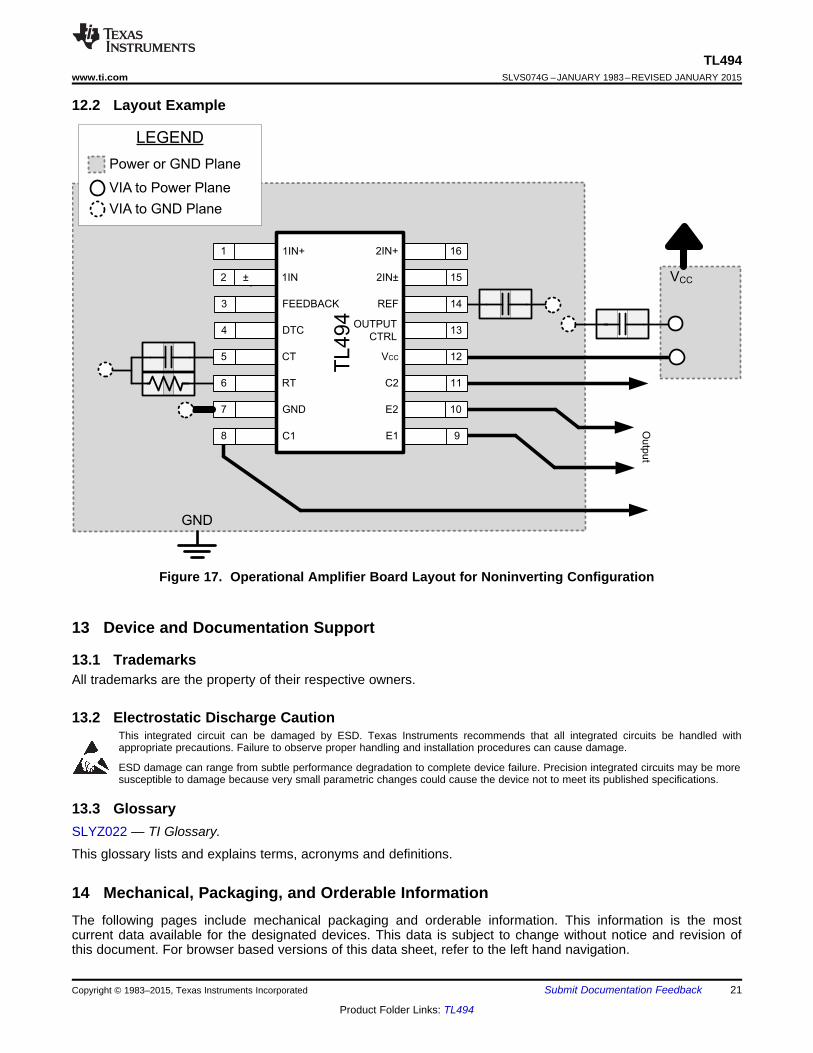
TL494www.ti.com SLVS074G –JANUARY 1983–REVISED JANUARY 2015
12.2 Layout Example
Figure 17. Operational Amplifier Board Layout for Noninverting Configuration
13 Device and Documentation Support
13.1 TrademarksAll trademarks are the property of their respective owners.
13.2 Electrostatic Discharge CautionThis integrated circuit can be damaged by ESD. Texas Instruments recommends that all integrated circuits be handled withappropriate precautions. Failure to observe proper handling and installation procedures can cause damage.
ESD damage can range from subtle performance degradation to complete device failure. Precision integrated circuits may be moresusceptible to damage because very small parametric changes could cause the device not to meet its published specifications.
13.3 GlossarySLYZ022 — TI Glossary.
This glossary lists and explains terms, acronyms and definitions.
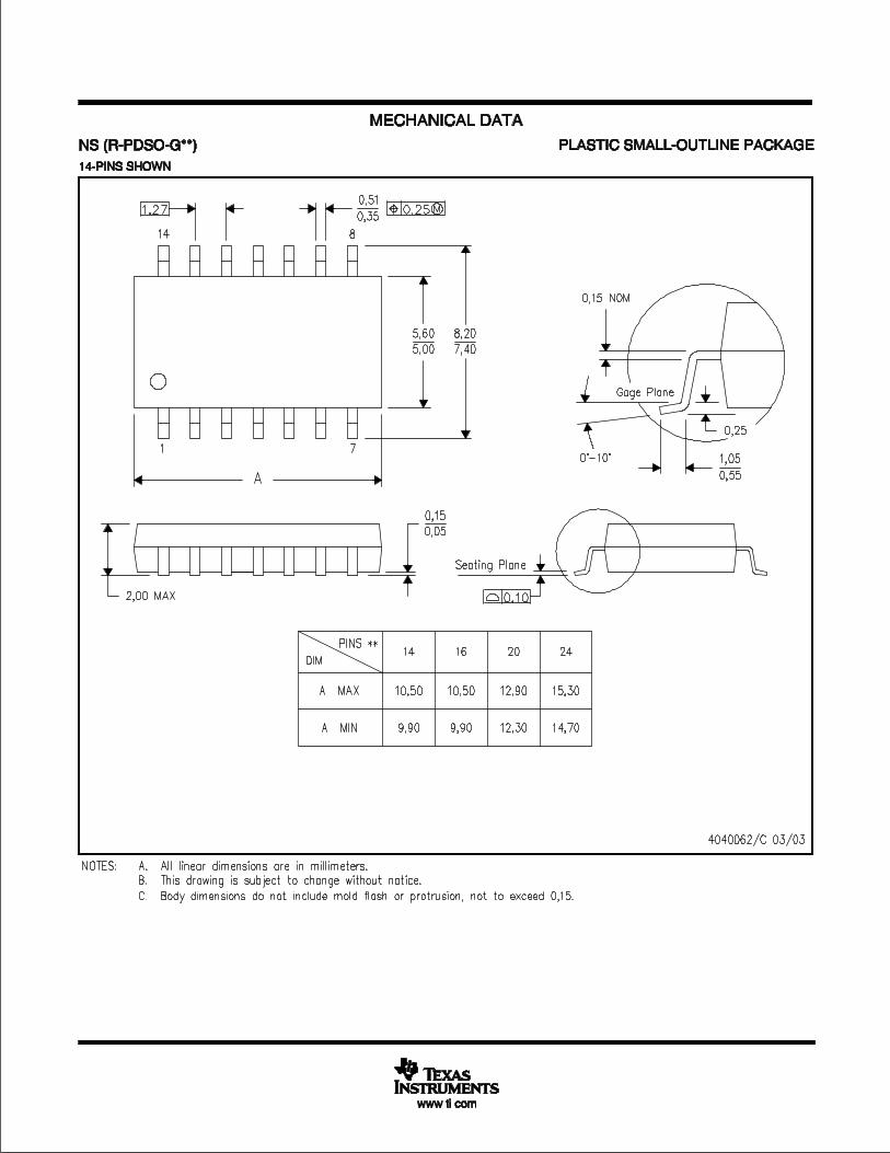
14 Mechanical, Packaging, and Orderable InformationThe following pages include mechanical packaging and orderable information. This information is the mostcurrent data available for the designated devices. This data is subject to change without notice and revision ofthis document. For browser based versions of this data sheet, refer to the left hand navigation.
Copyright © 1983–2015, Texas Instruments Incorporated Submit Documentation Feedback 21
Product Folder Links: TL494
PACKAGE OPTION ADDENDUM
www.ti.com 10-Jun-2014
Addendum-Page 1
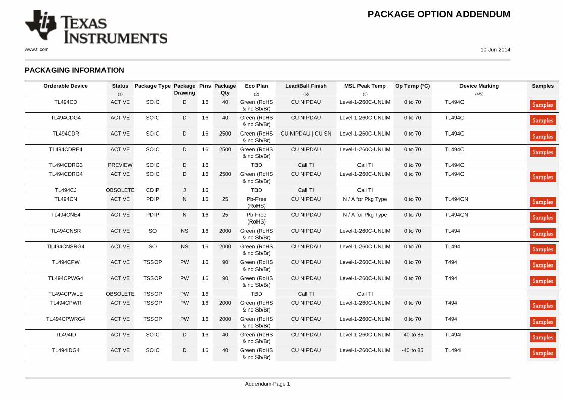
PACKAGING INFORMATION
Orderable Device Status(1)
Package Type PackageDrawing
Pins PackageQty
Eco Plan(2)
Lead/Ball Finish(6)
MSL Peak Temp(3)
Op Temp (°C) Device Marking(4/5)
Samples
TL494CD ACTIVE SOIC D 16 40 Green (RoHS& no Sb/Br)
CU NIPDAU Level-1-260C-UNLIM 0 to 70 TL494C
TL494CDG4 ACTIVE SOIC D 16 40 Green (RoHS& no Sb/Br)
CU NIPDAU Level-1-260C-UNLIM 0 to 70 TL494C
TL494CDR ACTIVE SOIC D 16 2500 Green (RoHS& no Sb/Br)
CU NIPDAU | CU SN Level-1-260C-UNLIM 0 to 70 TL494C
TL494CDRE4 ACTIVE SOIC D 16 2500 Green (RoHS& no Sb/Br)
CU NIPDAU Level-1-260C-UNLIM 0 to 70 TL494C
TL494CDRG3 PREVIEW SOIC D 16 TBD Call TI Call TI 0 to 70 TL494C
TL494CDRG4 ACTIVE SOIC D 16 2500 Green (RoHS& no Sb/Br)
CU NIPDAU Level-1-260C-UNLIM 0 to 70 TL494C
TL494CJ OBSOLETE CDIP J 16 TBD Call TI Call TI
TL494CN ACTIVE PDIP N 16 25 Pb-Free(RoHS)
CU NIPDAU N / A for Pkg Type 0 to 70 TL494CN
TL494CNE4 ACTIVE PDIP N 16 25 Pb-Free(RoHS)
CU NIPDAU N / A for Pkg Type 0 to 70 TL494CN
TL494CNSR ACTIVE SO NS 16 2000 Green (RoHS& no Sb/Br)
CU NIPDAU Level-1-260C-UNLIM 0 to 70 TL494
TL494CNSRG4 ACTIVE SO NS 16 2000 Green (RoHS& no Sb/Br)
CU NIPDAU Level-1-260C-UNLIM 0 to 70 TL494
TL494CPW ACTIVE TSSOP PW 16 90 Green (RoHS& no Sb/Br)
CU NIPDAU Level-1-260C-UNLIM 0 to 70 T494
TL494CPWG4 ACTIVE TSSOP PW 16 90 Green (RoHS& no Sb/Br)
CU NIPDAU Level-1-260C-UNLIM 0 to 70 T494
TL494CPWLE OBSOLETE TSSOP PW 16 TBD Call TI Call TI
TL494CPWR ACTIVE TSSOP PW 16 2000 Green (RoHS& no Sb/Br)
CU NIPDAU Level-1-260C-UNLIM 0 to 70 T494
TL494CPWRG4 ACTIVE TSSOP PW 16 2000 Green (RoHS& no Sb/Br)
CU NIPDAU Level-1-260C-UNLIM 0 to 70 T494
TL494ID ACTIVE SOIC D 16 40 Green (RoHS& no Sb/Br)
CU NIPDAU Level-1-260C-UNLIM -40 to 85 TL494I
TL494IDG4 ACTIVE SOIC D 16 40 Green (RoHS& no Sb/Br)
CU NIPDAU Level-1-260C-UNLIM -40 to 85 TL494I
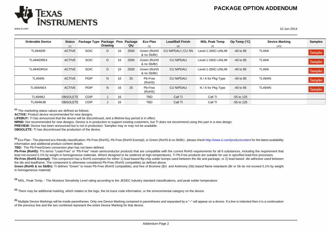
PACKAGE OPTION ADDENDUM
www.ti.com 10-Jun-2014
Addendum-Page 2
Orderable Device Status(1)
Package Type PackageDrawing
Pins PackageQty
Eco Plan(2)
Lead/Ball Finish(6)
MSL Peak Temp(3)
Op Temp (°C) Device Marking(4/5)
Samples
TL494IDR ACTIVE SOIC D 16 2500 Green (RoHS& no Sb/Br)
CU NIPDAU | CU SN Level-1-260C-UNLIM -40 to 85 TL494I
TL494IDRE4 ACTIVE SOIC D 16 2500 Green (RoHS& no Sb/Br)
CU NIPDAU Level-1-260C-UNLIM -40 to 85 TL494I
TL494IDRG4 ACTIVE SOIC D 16 2500 Green (RoHS& no Sb/Br)
CU NIPDAU Level-1-260C-UNLIM -40 to 85 TL494I
TL494IN ACTIVE PDIP N 16 25 Pb-Free(RoHS)
CU NIPDAU N / A for Pkg Type -40 to 85 TL494IN
TL494INE4 ACTIVE PDIP N 16 25 Pb-Free(RoHS)
CU NIPDAU N / A for Pkg Type -40 to 85 TL494IN
TL494MJ OBSOLETE CDIP J 16 TBD Call TI Call TI -55 to 125
TL494MJB OBSOLETE CDIP J 16 TBD Call TI Call TI -55 to 125 (1) The marketing status values are defined as follows:ACTIVE: Product device recommended for new designs.LIFEBUY: TI has announced that the device will be discontinued, and a lifetime-buy period is in effect.NRND: Not recommended for new designs. Device is in production to support existing customers, but TI does not recommend using this part in a new design.PREVIEW: Device has been announced but is not in production. Samples may or may not be available.OBSOLETE: TI has discontinued the production of the device.
(2) Eco Plan - The planned eco-friendly classification: Pb-Free (RoHS), Pb-Free (RoHS Exempt), or Green (RoHS & no Sb/Br) - please check http://www.ti.com/productcontent for the latest availabilityinformation and additional product content details.TBD: The Pb-Free/Green conversion plan has not been defined.Pb-Free (RoHS): TI's terms "Lead-Free" or "Pb-Free" mean semiconductor products that are compatible with the current RoHS requirements for all 6 substances, including the requirement thatlead not exceed 0.1% by weight in homogeneous materials. Where designed to be soldered at high temperatures, TI Pb-Free products are suitable for use in specified lead-free processes.Pb-Free (RoHS Exempt): This component has a RoHS exemption for either 1) lead-based flip-chip solder bumps used between the die and package, or 2) lead-based die adhesive used betweenthe die and leadframe. The component is otherwise considered Pb-Free (RoHS compatible) as defined above.Green (RoHS & no Sb/Br): TI defines "Green" to mean Pb-Free (RoHS compatible), and free of Bromine (Br) and Antimony (Sb) based flame retardants (Br or Sb do not exceed 0.1% by weightin homogeneous material)
(3) MSL, Peak Temp. - The Moisture Sensitivity Level rating according to the JEDEC industry standard classifications, and peak solder temperature.
(4) There may be additional marking, which relates to the logo, the lot trace code information, or the environmental category on the device.
(5) Multiple Device Markings will be inside parentheses. Only one Device Marking contained in parentheses and separated by a "~" will appear on a device. If a line is indented then it is a continuationof the previous line and the two combined represent the entire Device Marking for that device.
PACKAGE OPTION ADDENDUM
www.ti.com 10-Jun-2014
Addendum-Page 3
(6) Lead/Ball Finish - Orderable Devices may have multiple material finish options. Finish options are separated by a vertical ruled line. Lead/Ball Finish values may wrap to two lines if the finishvalue exceeds the maximum column width.
Important Information and Disclaimer:The information provided on this page represents TI's knowledge and belief as of the date that it is provided. TI bases its knowledge and belief on informationprovided by third parties, and makes no representation or warranty as to the accuracy of such information. Efforts are underway to better integrate information from third parties. TI has taken andcontinues to take reasonable steps to provide representative and accurate information but may not have conducted destructive testing or chemical analysis on incoming materials and chemicals.TI and TI suppliers consider certain information to be proprietary, and thus CAS numbers and other limited information may not be available for release.
In no event shall TI's liability arising out of such information exceed the total purchase price of the TI part(s) at issue in this document sold by TI to Customer on an annual basis.
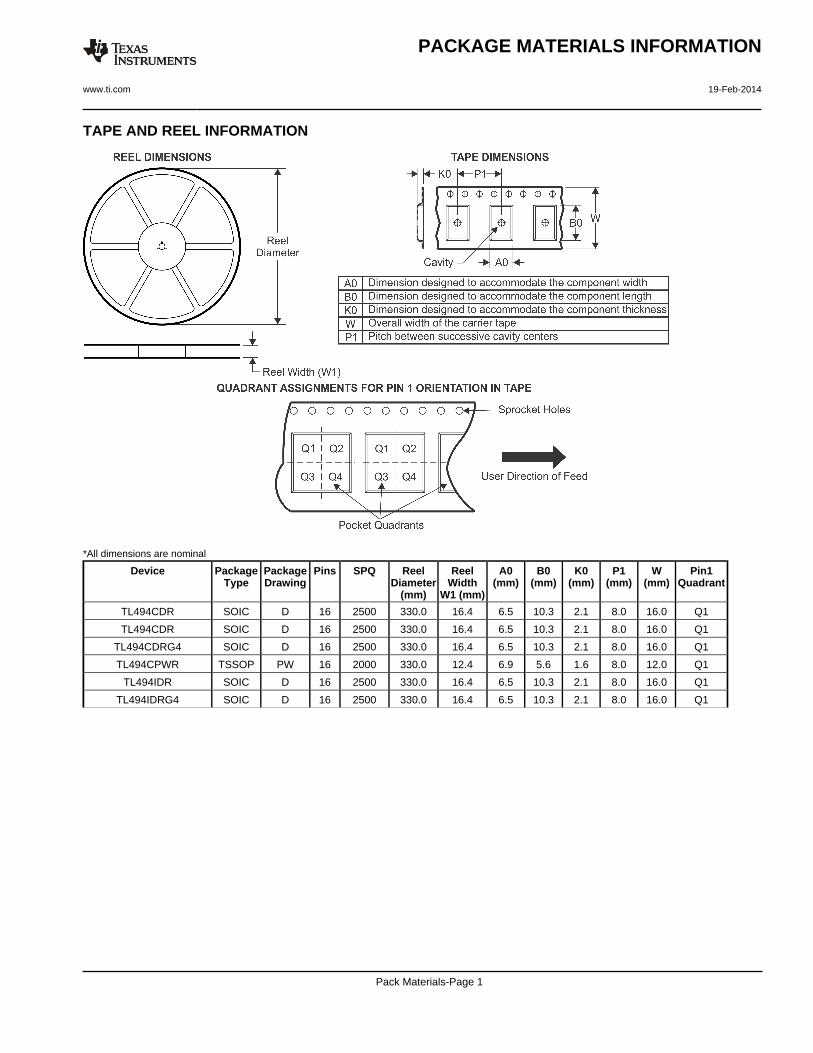
TAPE AND REEL INFORMATION
*All dimensions are nominal
Device PackageType
PackageDrawing
Pins SPQ ReelDiameter
(mm)
ReelWidth
W1 (mm)
A0(mm)
B0(mm)
K0(mm)
P1(mm)
W(mm)
Pin1Quadrant
TL494CDR SOIC D 16 2500 330.0 16.4 6.5 10.3 2.1 8.0 16.0 Q1
TL494CDR SOIC D 16 2500 330.0 16.4 6.5 10.3 2.1 8.0 16.0 Q1
TL494CDRG4 SOIC D 16 2500 330.0 16.4 6.5 10.3 2.1 8.0 16.0 Q1
TL494CPWR TSSOP PW 16 2000 330.0 12.4 6.9 5.6 1.6 8.0 12.0 Q1
TL494IDR SOIC D 16 2500 330.0 16.4 6.5 10.3 2.1 8.0 16.0 Q1
TL494IDRG4 SOIC D 16 2500 330.0 16.4 6.5 10.3 2.1 8.0 16.0 Q1
PACKAGE MATERIALS INFORMATION
www.ti.com 19-Feb-2014
Pack Materials-Page 1
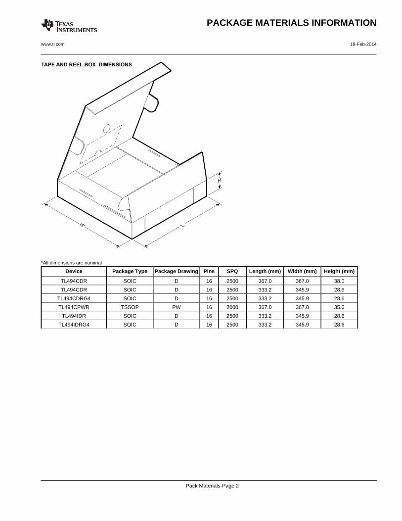
*All dimensions are nominal
Device Package Type Package Drawing Pins SPQ Length (mm) Width (mm) Height (mm)
TL494CDR SOIC D 16 2500 367.0 367.0 38.0
TL494CDR SOIC D 16 2500 333.2 345.9 28.6
TL494CDRG4 SOIC D 16 2500 333.2 345.9 28.6
TL494CPWR TSSOP PW 16 2000 367.0 367.0 35.0
TL494IDR SOIC D 16 2500 333.2 345.9 28.6
TL494IDRG4 SOIC D 16 2500 333.2 345.9 28.6
PACKAGE MATERIALS INFORMATION
www.ti.com 19-Feb-2014
Pack Materials-Page 2
IMPORTANT NOTICE
Texas Instruments Incorporated and its subsidiaries (TI) reserve the right to make corrections, enhancements, improvements and otherchanges to its semiconductor products and services per JESD46, latest issue, and to discontinue any product or service per JESD48, latestissue. Buyers should obtain the latest relevant information before placing orders and should verify that such information is current andcomplete. All semiconductor products (also referred to herein as “components”) are sold subject to TI’s terms and conditions of salesupplied at the time of order acknowledgment.TI warrants performance of its components to the specifications applicable at the time of sale, in accordance with the warranty in TI’s termsand conditions of sale of semiconductor products. Testing and other quality control techniques are used to the extent TI deems necessaryto support this warranty. Except where mandated by applicable law, testing of all parameters of each component is not necessarilyperformed.TI assumes no liability for applications assistance or the design of Buyers’ products. Buyers are responsible for their products andapplications using TI components. To minimize the risks associated with Buyers’ products and applications, Buyers should provideadequate design and operating safeguards.TI does not warrant or represent that any license, either express or implied, is granted under any patent right, copyright, mask work right, orother intellectual property right relating to any combination, machine, or process in which TI components or services are used. Informationpublished by TI regarding third-party products or services does not constitute a license to use such products or services or a warranty orendorsement thereof. Use of such information may require a license from a third party under the patents or other intellectual property of thethird party, or a license from TI under the patents or other intellectual property of TI.Reproduction of significant portions of TI information in TI data books or data sheets is permissible only if reproduction is without alterationand is accompanied by all associated warranties, conditions, limitations, and notices. TI is not responsible or liable for such altereddocumentation. Information of third parties may be subject to additional restrictions.Resale of TI components or services with statements different from or beyond the parameters stated by TI for that component or servicevoids all express and any implied warranties for the associated TI component or service and is an unfair and deceptive business practice.TI is not responsible or liable for any such statements.Buyer acknowledges and agrees that it is solely responsible for compliance with all legal, regulatory and safety-related requirementsconcerning its products, and any use of TI components in its applications, notwithstanding any applications-related information or supportthat may be provided by TI. Buyer represents and agrees that it has all the necessary expertise to create and implement safeguards whichanticipate dangerous consequences of failures, monitor failures and their consequences, lessen the likelihood of failures that might causeharm and take appropriate remedial actions. Buyer will fully indemnify TI and its representatives against any damages arising out of the useof any TI components in safety-critical applications.In some cases, TI components may be promoted specifically to facilitate safety-related applications. With such components, TI’s goal is tohelp enable customers to design and create their own end-product solutions that meet applicable functional safety standards andrequirements. Nonetheless, such components are subject to these terms.No TI components are authorized for use in FDA Class III (or similar life-critical medical equipment) unless authorized officers of the partieshave executed a special agreement specifically governing such use.Only those TI components which TI has specifically designated as military grade or “enhanced plastic” are designed and intended for use inmilitary/aerospace applications or environments. Buyer acknowledges and agrees that any military or aerospace use of TI componentswhich have not been so designated is solely at the Buyer's risk, and that Buyer is solely responsible for compliance with all legal andregulatory requirements in connection with such use.TI has specifically designated certain components as meeting ISO/TS16949 requirements, mainly for automotive use. In any case of use ofnon-designated products, TI will not be responsible for any failure to meet ISO/TS16949.
Products ApplicationsAudio www.ti.com/audio Automotive and Transportation www.ti.com/automotiveAmplifiers amplifier.ti.com Communications and Telecom www.ti.com/communicationsData Converters dataconverter.ti.com Computers and Peripherals www.ti.com/computersDLP® Products www.dlp.com Consumer Electronics www.ti.com/consumer-appsDSP dsp.ti.com Energy and Lighting www.ti.com/energyClocks and Timers www.ti.com/clocks Industrial www.ti.com/industrialInterface interface.ti.com Medical www.ti.com/medicalLogic logic.ti.com Security www.ti.com/securityPower Mgmt power.ti.com Space, Avionics and Defense www.ti.com/space-avionics-defenseMicrocontrollers microcontroller.ti.com Video and Imaging www.ti.com/videoRFID www.ti-rfid.comOMAP Applications Processors www.ti.com/omap TI E2E Community e2e.ti.comWireless Connectivity www.ti.com/wirelessconnectivity
Mailing Address: Texas Instruments, Post Office Box 655303, Dallas, Texas 75265Copyright © 2015, Texas Instruments Incorporated


