Download - TLE92464ED - Infineon Technologies

TLE92464EDFour channel low-side solenoid driver IC
Quality Requirement Category: Automotive
Features• Four independent low side channels with integrated MOSFETs (RDSon = 115 mΩ)• <1% current control accuracy• Programmable setpoint from 0 mA to 1.5 A• Load current including dither 1.8 A• Current in parallel channel mode 2.7 A• Integrated dither generator with programmable amplitude, frequency and waveform• 15 bit current setpoint resolution• Integrated sense resistor RSHUNT = 140 mΩ• Excellent immunity to large load supply voltage changes• Operation down to 3.5 V at VDD pin• 32 bit SPI with 8 bit CRC and SPI watchdog• Sophisticated protection and diagnostic functions for each channel in on and off state
- Independent thermal shutdown for each channel- Diagnostic Function (Open Load, Short Circuit Ground, Overcurrent) - Voltage monitoring- Overtemperature protection
• Two independent current feedback paths• Integrated system clock with clock watchdog• Temperature range -40°C to 175 °C• Small power package PG-DSO-36-72• Green Product (RoHS compliant)• Pb-free (RoHS compliant) package• AEC-Q100 Grade 0 qualified• ISO 26262 Safety Element out of Context for safety requirements up to ASIL C
Potential applications• Variable force solenoids (e.g. automatic transmission solenoids)• Other constant current solenoids
- Idle air control- Exhaust gas recirculation- Vapor management valve- Suspension control
Product validationQualified for automotive applications with higher temperature requirements. Product validation according toAEC-Q100.
Datasheet Please read the Important Notice and Warnings at the end of this document Rev. 1.1www.infineon.com 2020-11-20

Product type & package tableProduct type Package
TLE92464ED PG-DSO-36-72 Dual-Gauge (300 mil)
DescriptionThe TLE92464ED is a flexible, monolithic solenoid driver IC designed for the control of linear solenoids inautomatic transmissions, electronic stability control and active suspension applications. The device includesthe drive transistors and the current sensing resistors to minimize the number of external components.The device controls the load current with less than 1% error. Target currents from 0 to 1500mA can beprogrammed with a resolution of 15 bit. The device supports dither currents up to 1800mA. The dithergenerator superimposes a triangular or trapezoidal waveform with programmable amplitude, frequency andshape on the programmed current setpoint. A 32 bit SPI interface is used to control the 4 channels and monitorthe status of the diagnostic functions. The SPI communication is secured with an 8 bit CRC and a programmabletimeout watchdog.An active low reset input (RESN) is used to disable all channels and reset the internal registers to the defaultvalues. An active high enable pin (EN) enables or disables the output channels without disabling the SPIinterface. A fault output pin (FAULTN) signal can be used as external interrupt to the microcontroller whenever afault is detected.
Product type & package table
Datasheet 2 Rev. 1.12020-11-20
TLE92464ED Four channel low-side solenoid driver IC

Table of contents
Features . . . . . . . . . . . . . . . . . . . . . . . . . . . . . . . . . . . . . . . . . . . . . . . . . . . . . . . . . . . . . . . . . . . . . . . . . . . . . . . 1
Potential applications . . . . . . . . . . . . . . . . . . . . . . . . . . . . . . . . . . . . . . . . . . . . . . . . . . . . . . . . . . . . . . . . . . 1
Product validation . . . . . . . . . . . . . . . . . . . . . . . . . . . . . . . . . . . . . . . . . . . . . . . . . . . . . . . . . . . . . . . . . . . . . .1
Product type & package table . . . . . . . . . . . . . . . . . . . . . . . . . . . . . . . . . . . . . . . . . . . . . . . . . . . . . . . . . . . 2
Description . . . . . . . . . . . . . . . . . . . . . . . . . . . . . . . . . . . . . . . . . . . . . . . . . . . . . . . . . . . . . . . . . . . . . . . . . . . . .2
Table of contents . . . . . . . . . . . . . . . . . . . . . . . . . . . . . . . . . . . . . . . . . . . . . . . . . . . . . . . . . . . . . . . . . . . . . . . 3
1 Block diagram . . . . . . . . . . . . . . . . . . . . . . . . . . . . . . . . . . . . . . . . . . . . . . . . . . . . . . . . . . . . . . . . . . . . . . . . . . 6
2 Pin configuration . . . . . . . . . . . . . . . . . . . . . . . . . . . . . . . . . . . . . . . . . . . . . . . . . . . . . . . . . . . . . . . . . . . . . . . 7
3 Electrial characteristics and parameters . . . . . . . . . . . . . . . . . . . . . . . . . . . . . . . . . . . . . . . . . . . . . . . . . 93.1 Absolute maximum ratings . . . . . . . . . . . . . . . . . . . . . . . . . . . . . . . . . . . . . . . . . . . . . . . . . . . . . . . . . . . . . . . 93.1.1 Absolute maximum voltage ratings . . . . . . . . . . . . . . . . . . . . . . . . . . . . . . . . . . . . . . . . . . . . . . . . . . . . . . 93.1.2 Absolute maximum current ratings . . . . . . . . . . . . . . . . . . . . . . . . . . . . . . . . . . . . . . . . . . . . . . . . . . . . . 103.1.3 Absolute maximum temperature ratings . . . . . . . . . . . . . . . . . . . . . . . . . . . . . . . . . . . . . . . . . . . . . . . . 103.1.4 ESD Robustness . . . . . . . . . . . . . . . . . . . . . . . . . . . . . . . . . . . . . . . . . . . . . . . . . . . . . . . . . . . . . . . . . . . . . . 113.2 Functional range . . . . . . . . . . . . . . . . . . . . . . . . . . . . . . . . . . . . . . . . . . . . . . . . . . . . . . . . . . . . . . . . . . . . . . . 113.2.1 Functional range . . . . . . . . . . . . . . . . . . . . . . . . . . . . . . . . . . . . . . . . . . . . . . . . . . . . . . . . . . . . . . . . . . . . . 113.2.2 Parameter above 150°C . . . . . . . . . . . . . . . . . . . . . . . . . . . . . . . . . . . . . . . . . . . . . . . . . . . . . . . . . . . . . . . .133.2.3 Thermal resistance . . . . . . . . . . . . . . . . . . . . . . . . . . . . . . . . . . . . . . . . . . . . . . . . . . . . . . . . . . . . . . . . . . . 13
4 Functional description . . . . . . . . . . . . . . . . . . . . . . . . . . . . . . . . . . . . . . . . . . . . . . . . . . . . . . . . . . . . . . . . . 144.1 Power supply . . . . . . . . . . . . . . . . . . . . . . . . . . . . . . . . . . . . . . . . . . . . . . . . . . . . . . . . . . . . . . . . . . . . . . . . . . 144.1.1 Voltage monitoring . . . . . . . . . . . . . . . . . . . . . . . . . . . . . . . . . . . . . . . . . . . . . . . . . . . . . . . . . . . . . . . . . . . 144.1.2 Electrical characteristics power supply . . . . . . . . . . . . . . . . . . . . . . . . . . . . . . . . . . . . . . . . . . . . . . . . . .154.2 Input / Output . . . . . . . . . . . . . . . . . . . . . . . . . . . . . . . . . . . . . . . . . . . . . . . . . . . . . . . . . . . . . . . . . . . . . . . . . .174.2.1 Clock . . . . . . . . . . . . . . . . . . . . . . . . . . . . . . . . . . . . . . . . . . . . . . . . . . . . . . . . . . . . . . . . . . . . . . . . . . . . . . . . 174.2.2 Clock Watchdog . . . . . . . . . . . . . . . . . . . . . . . . . . . . . . . . . . . . . . . . . . . . . . . . . . . . . . . . . . . . . . . . . . . . . . 184.2.3 I/O Pins . . . . . . . . . . . . . . . . . . . . . . . . . . . . . . . . . . . . . . . . . . . . . . . . . . . . . . . . . . . . . . . . . . . . . . . . . . . . . . 184.2.4 Electrical characteristics I/O . . . . . . . . . . . . . . . . . . . . . . . . . . . . . . . . . . . . . . . . . . . . . . . . . . . . . . . . . . . 194.3 IC Operation states . . . . . . . . . . . . . . . . . . . . . . . . . . . . . . . . . . . . . . . . . . . . . . . . . . . . . . . . . . . . . . . . . . . . . 214.4 Channel modes . . . . . . . . . . . . . . . . . . . . . . . . . . . . . . . . . . . . . . . . . . . . . . . . . . . . . . . . . . . . . . . . . . . . . . . . 234.5 Power stages . . . . . . . . . . . . . . . . . . . . . . . . . . . . . . . . . . . . . . . . . . . . . . . . . . . . . . . . . . . . . . . . . . . . . . . . . . .244.5.1 Channel overview . . . . . . . . . . . . . . . . . . . . . . . . . . . . . . . . . . . . . . . . . . . . . . . . . . . . . . . . . . . . . . . . . . . . 244.5.2 Parallel channel operation . . . . . . . . . . . . . . . . . . . . . . . . . . . . . . . . . . . . . . . . . . . . . . . . . . . . . . . . . . . . .254.5.3 Electrical characteristics power stages . . . . . . . . . . . . . . . . . . . . . . . . . . . . . . . . . . . . . . . . . . . . . . . . . . 264.6 Current control . . . . . . . . . . . . . . . . . . . . . . . . . . . . . . . . . . . . . . . . . . . . . . . . . . . . . . . . . . . . . . . . . . . . . . . . .274.6.1 Average current setpoint . . . . . . . . . . . . . . . . . . . . . . . . . . . . . . . . . . . . . . . . . . . . . . . . . . . . . . . . . . . . . . 274.6.2 Integrating Current Controller (ICC) . . . . . . . . . . . . . . . . . . . . . . . . . . . . . . . . . . . . . . . . . . . . . . . . . . . . .284.6.3 Electrical characteristics current control . . . . . . . . . . . . . . . . . . . . . . . . . . . . . . . . . . . . . . . . . . . . . . . . 33
Table of contents
Datasheet 3 Rev. 1.12020-11-20
TLE92464ED Four channel low-side solenoid driver IC

4.7 Dither . . . . . . . . . . . . . . . . . . . . . . . . . . . . . . . . . . . . . . . . . . . . . . . . . . . . . . . . . . . . . . . . . . . . . . . . . . . . . . . . . 344.7.1 Dither configuration . . . . . . . . . . . . . . . . . . . . . . . . . . . . . . . . . . . . . . . . . . . . . . . . . . . . . . . . . . . . . . . . . . 344.7.2 Dither parameter update . . . . . . . . . . . . . . . . . . . . . . . . . . . . . . . . . . . . . . . . . . . . . . . . . . . . . . . . . . . . . . 354.7.3 Dither PWM Synchronization . . . . . . . . . . . . . . . . . . . . . . . . . . . . . . . . . . . . . . . . . . . . . . . . . . . . . . . . . . .354.7.4 Dither Setpoint Synchronization . . . . . . . . . . . . . . . . . . . . . . . . . . . . . . . . . . . . . . . . . . . . . . . . . . . . . . . 374.7.5 Deep dither . . . . . . . . . . . . . . . . . . . . . . . . . . . . . . . . . . . . . . . . . . . . . . . . . . . . . . . . . . . . . . . . . . . . . . . . . . 374.8 Direct Drive . . . . . . . . . . . . . . . . . . . . . . . . . . . . . . . . . . . . . . . . . . . . . . . . . . . . . . . . . . . . . . . . . . . . . . . . . . . . 374.9 Diagnostic functions . . . . . . . . . . . . . . . . . . . . . . . . . . . . . . . . . . . . . . . . . . . . . . . . . . . . . . . . . . . . . . . . . . . . 384.9.1 Overview . . . . . . . . . . . . . . . . . . . . . . . . . . . . . . . . . . . . . . . . . . . . . . . . . . . . . . . . . . . . . . . . . . . . . . . . . . . . 384.9.2 Open Load/Short to Ground (OLSG) . . . . . . . . . . . . . . . . . . . . . . . . . . . . . . . . . . . . . . . . . . . . . . . . . . . . 404.9.3 OLSG Warning . . . . . . . . . . . . . . . . . . . . . . . . . . . . . . . . . . . . . . . . . . . . . . . . . . . . . . . . . . . . . . . . . . . . . . . . 424.9.4 Open Load (OL) . . . . . . . . . . . . . . . . . . . . . . . . . . . . . . . . . . . . . . . . . . . . . . . . . . . . . . . . . . . . . . . . . . . . . . .434.9.5 Short circuit ground (SG) . . . . . . . . . . . . . . . . . . . . . . . . . . . . . . . . . . . . . . . . . . . . . . . . . . . . . . . . . . . . . . 444.9.6 Overcurrent (OC) . . . . . . . . . . . . . . . . . . . . . . . . . . . . . . . . . . . . . . . . . . . . . . . . . . . . . . . . . . . . . . . . . . . . . 454.9.7 Register/OTP ECC . . . . . . . . . . . . . . . . . . . . . . . . . . . . . . . . . . . . . . . . . . . . . . . . . . . . . . . . . . . . . . . . . . . . . 454.9.8 Built in Self Test (BIST) . . . . . . . . . . . . . . . . . . . . . . . . . . . . . . . . . . . . . . . . . . . . . . . . . . . . . . . . . . . . . . . . 464.9.9 Electrical characteristics diagnostic functions . . . . . . . . . . . . . . . . . . . . . . . . . . . . . . . . . . . . . . . . . . . 474.10 Current supervision . . . . . . . . . . . . . . . . . . . . . . . . . . . . . . . . . . . . . . . . . . . . . . . . . . . . . . . . . . . . . . . . . . . . .484.10.1 Independent current feedback . . . . . . . . . . . . . . . . . . . . . . . . . . . . . . . . . . . . . . . . . . . . . . . . . . . . . . . . . 484.10.2 Average feedback values . . . . . . . . . . . . . . . . . . . . . . . . . . . . . . . . . . . . . . . . . . . . . . . . . . . . . . . . . . . . . . 494.10.3 Update/Freeze Mechanism . . . . . . . . . . . . . . . . . . . . . . . . . . . . . . . . . . . . . . . . . . . . . . . . . . . . . . . . . . . . 504.10.4 Iavg16, minimum/maximum current/PWM feedback . . . . . . . . . . . . . . . . . . . . . . . . . . . . . . . . . . . . . 514.11 Protection functions . . . . . . . . . . . . . . . . . . . . . . . . . . . . . . . . . . . . . . . . . . . . . . . . . . . . . . . . . . . . . . . . . . . . 524.11.1 Overtemperature protection . . . . . . . . . . . . . . . . . . . . . . . . . . . . . . . . . . . . . . . . . . . . . . . . . . . . . . . . . . . 524.11.2 Overcurrent protection . . . . . . . . . . . . . . . . . . . . . . . . . . . . . . . . . . . . . . . . . . . . . . . . . . . . . . . . . . . . . . . . 524.11.3 Electrical characteristics protection functions . . . . . . . . . . . . . . . . . . . . . . . . . . . . . . . . . . . . . . . . . . . 53
5 Serial peripheral interface (SPI) . . . . . . . . . . . . . . . . . . . . . . . . . . . . . . . . . . . . . . . . . . . . . . . . . . . . . . . . 545.1 Description of interface . . . . . . . . . . . . . . . . . . . . . . . . . . . . . . . . . . . . . . . . . . . . . . . . . . . . . . . . . . . . . . . . . 545.1.1 Cyclic redundancy check (CRC) . . . . . . . . . . . . . . . . . . . . . . . . . . . . . . . . . . . . . . . . . . . . . . . . . . . . . . . . .545.1.2 Timing diagram . . . . . . . . . . . . . . . . . . . . . . . . . . . . . . . . . . . . . . . . . . . . . . . . . . . . . . . . . . . . . . . . . . . . . . 555.1.3 Electrical characteristics SPI interface . . . . . . . . . . . . . . . . . . . . . . . . . . . . . . . . . . . . . . . . . . . . . . . . . . 555.2 Description of protocol . . . . . . . . . . . . . . . . . . . . . . . . . . . . . . . . . . . . . . . . . . . . . . . . . . . . . . . . . . . . . . . . . .575.2.1 Data flow . . . . . . . . . . . . . . . . . . . . . . . . . . . . . . . . . . . . . . . . . . . . . . . . . . . . . . . . . . . . . . . . . . . . . . . . . . . . 575.2.2 SPI watchdog . . . . . . . . . . . . . . . . . . . . . . . . . . . . . . . . . . . . . . . . . . . . . . . . . . . . . . . . . . . . . . . . . . . . . . . . 575.3 SPI frame definition . . . . . . . . . . . . . . . . . . . . . . . . . . . . . . . . . . . . . . . . . . . . . . . . . . . . . . . . . . . . . . . . . . . . 585.3.1 MOSI - Write frame . . . . . . . . . . . . . . . . . . . . . . . . . . . . . . . . . . . . . . . . . . . . . . . . . . . . . . . . . . . . . . . . . . . . 585.3.2 MOSI - Read frame . . . . . . . . . . . . . . . . . . . . . . . . . . . . . . . . . . . . . . . . . . . . . . . . . . . . . . . . . . . . . . . . . . . . 595.3.3 MISO - 16 bit reply frame . . . . . . . . . . . . . . . . . . . . . . . . . . . . . . . . . . . . . . . . . . . . . . . . . . . . . . . . . . . . . . 605.3.4 MISO - 22 bit reply frame . . . . . . . . . . . . . . . . . . . . . . . . . . . . . . . . . . . . . . . . . . . . . . . . . . . . . . . . . . . . . . 615.3.5 MISO - Critical fault reply frame . . . . . . . . . . . . . . . . . . . . . . . . . . . . . . . . . . . . . . . . . . . . . . . . . . . . . . . . 625.4 Register description . . . . . . . . . . . . . . . . . . . . . . . . . . . . . . . . . . . . . . . . . . . . . . . . . . . . . . . . . . . . . . . . . . . . 63
Table of contents
Datasheet 4 Rev. 1.12020-11-20
TLE92464ED Four channel low-side solenoid driver IC
5.4.1 Overview of Register Types . . . . . . . . . . . . . . . . . . . . . . . . . . . . . . . . . . . . . . . . . . . . . . . . . . . . . . . . . . . . 635.4.2 Central registers . . . . . . . . . . . . . . . . . . . . . . . . . . . . . . . . . . . . . . . . . . . . . . . . . . . . . . . . . . . . . . . . . . . . . .645.4.3 Channel registers . . . . . . . . . . . . . . . . . . . . . . . . . . . . . . . . . . . . . . . . . . . . . . . . . . . . . . . . . . . . . . . . . . . . . 94
6 Application information . . . . . . . . . . . . . . . . . . . . . . . . . . . . . . . . . . . . . . . . . . . . . . . . . . . . . . . . . . . . . . 114
7 Package dimensions . . . . . . . . . . . . . . . . . . . . . . . . . . . . . . . . . . . . . . . . . . . . . . . . . . . . . . . . . . . . . . . . . . 115
Revision history . . . . . . . . . . . . . . . . . . . . . . . . . . . . . . . . . . . . . . . . . . . . . . . . . . . . . . . . . . . . . . . . . . . . . . 116
Disclaimer . . . . . . . . . . . . . . . . . . . . . . . . . . . . . . . . . . . . . . . . . . . . . . . . . . . . . . . . . . . . . . . . . . . . . . . . . . . 117
Table of contents
Datasheet 5 Rev. 1.12020-11-20
TLE92464ED Four channel low-side solenoid driver IC

1 Block diagram
Power Supply
Undervoltage/Overvoltage Detection
PLL with Watchdog
Central Logic
CLK
VBAT
VDD
GND
RESN
SPIWatchdog
SPI
EN
SI
VIO
SCK
CSN
SO
DRV0
DRV1
DRV2
DRV3
Four Channel low-side Solenoid Driver IC
FAULTN
Channel Logic,
Current Control,Dither
CurrentSense
LoadDiagnosis
Temperature Sense
Low SideGate Control
Overcurrent Protection FWD0
LOAD0
GNDP0
Rshunt0
DMOS0
Channel Logic,
Current Control,Dither
CurrentSense
LoadDiagnosis
Temperature Sense
Low SideGate Control
Overcurrent Protection FWD1
LOAD1
GNDP1
Rshunt1
DMOS1
Channel Logic,
Current Control,Dither
CurrentSense
LoadDiagnosis
Temperature Sense
Low SideGate Control
Overcurrent Protection FWD2
LOAD2
GNDP2
Rshunt2
DMOS2
Channel Logic,
Current Control,Dither
CurrentSense
LoadDiagnosis
Temperature Sense
Low SideGate Control
Overcurrent Protection FWD3
LOAD3
GNDP3
Rshunt3
DMOS3
Figure 1 Block diagram
Block diagram
Datasheet 6 Rev. 1.12020-11-20
TLE92464ED Four channel low-side solenoid driver IC

2 Pin configuration
LOAD3FWD3GNDP3GNDVBATGNDGNDVDDDRV3DRV2DRV1
CLKGND
EN GNDGNDP2FWD2LOAD2
LOAD0FWD0
GNDP0GND
SO
SISCKCSN
DRV0
GNDRESNGND
FAULTNGND
GNDP1FWD1
LOAD1
363534333231302928272625242322212019
123456789101112131415161718
VIO
Figure 2 Pin assignment
Pin definitions and functions
Table 1 Pin definition and functions
Pin Symbol Function
1 LOAD0 Output; for channel 0.
2 FWD0 Free wheeling diode; for channel 0.
3 GNDP0 Ground; for channel 0 power stage.
4 GND Ground; connect to GND.
5 CSN SPI chip select input; digital input: 3.3 V or 5.0 V logic levels.
6 SCK SPI clock input; digital input: 3.3 V or 5.0 V logic levels.
7 SI SPI input; digital input: 3.3 V or 5.0 V logic levels.
8 VIO Supply SPI Slave Out (SO) pin; connected to 3.3 V or 5.0 V supply.
9 SO SPI output; push pull output compatible to 3.3 V or 5.0 V logic levels.
10 GND Ground; signal ground. Internally connected to cooling tab.
11 RESN Control input; digital input: 3.3 V or 5.0 V logic levels. Active low reset input.
12 GND Ground; signal ground. Internally connected to cooling tab.
13 FAULTN Status output; open drain output. In case not used, keep open.
14 GND Ground; connect to GND.
15 EN Control input; digital input: 3.3 V or 5.0 V logic levels. Active high enable input.
16 GNDP1 Ground; ground connection for channel 1 power stage.
17 FWD1 Free wheeling diode; for channel 1.
18 LOAD1 Output; for channel 1.
19 LOAD2 Output; for channel 2.
Pin configuration
Datasheet 7 Rev. 1.12020-11-20
TLE92464ED Four channel low-side solenoid driver IC

Table 1 Pin definition and functions (continued)
Pin Symbol Function
20 FWD2 Free wheeling diode; for channel 2.
21 GNDP2 Ground; ground connection for channel 2 power stage.
22 GND Ground; connect to GND.
23 GND Ground; signal ground. Internally connected to cooling tab.
24 CLK Clock input; Main system clock.
25 DRV0 Direct drive input for channel 0: 3.3 V or 5.0 V logical levels.
26 DRV1 Direct drive input for channel 1: 3.3 V or 5.0 V logical levels.
27 DRV2 Direct drive input for channel 2: 3.3 V or 5.0 V logical levels.
28 DRV3 Direct drive input for channel 3: 3.3 V or 5.0 V logical levels.
29 VDD Supply voltage; supplies digital circuits. Connected to 5.0 V supply voltage.
30 GND Ground; signal ground. Internally connected to cooling tab.
31 GND Ground; connect to GND
32 VBAT Supply voltage; connected to battery voltage with reverse protection diode andfilter against EMC.
33 GND Ground; connect to GND.
34 GNDP3 Ground; for channel 3 power stage.
35 FWD3 Free wheeling diode; for channel 3.
36 LOAD3 Output; for channel 3.
37 Cooling Tap Connect externally to GND and heat sink area
Pin configuration
Datasheet 8 Rev. 1.12020-11-20
TLE92464ED Four channel low-side solenoid driver IC

3 Electrial characteristics and parameters
3.1 Absolute maximum ratings
3.1.1 Absolute maximum voltage ratings
Table 2 Absolute maximum voltage ratingsTJ = -40°C to 150°C; all voltages with respect to ground, positive current flowing into pin (unlessotherwise specified).
Parameter Symbol Values Unit Note or conditionMin. Typ. Max.
Max. supplyvoltage (VDD)
VDD,max -0.3 – 19 V
Max. supplyvoltage (VBAT)
VBAT,max -0.3 – 40 V
Max. supplyvoltage (VIO)
VVIO,max -0.3 – 19 V
Max. digitalinput pinvoltage (CLK,RESN, EN,DRVx, SCK,CSN, SI)
VCLK,maxVRESN,maxVEN,maxVDRVx,maxVSCK,maxVCSN,maxVSI,max
-0.3 – 19 V
Max. opendrain outputvoltage(FAULTN)
VFAULTN,max -0.3 – 19 V
Max. Push PullOuput (SO)
VSO,max -0.3 – 19 V
Max. LOADxvoltage
VLOADx,max -0.31) – 40 V 1) During negative pulses (VLOADx < -0.3V) the maximum energy of ELOADx = |-VLOADx*(ILOADx+IFWDx)*tpulse| <= 2 mJ shall not beviolated.
Max. FWDxvoltage
VFWDx,max -0.31) – 40 V 1) During negative pulses (VFWDx < -0.3V) the maximum energy of EFWDx = |-VFWDx*(ILOADx+IFWDx)*tpulse| <= 2 mJ shall not beviolated.
Max. GNDPxvoltage
VGNDPx,max -0.3 – 0.3 V
Electrial characteristics and parameters
Datasheet 9 Rev. 1.12020-11-20
TLE92464ED Four channel low-side solenoid driver IC

3.1.2 Absolute maximum current ratings
Table 3 Absolute maximum current ratingsTJ = -40°C to 150°C; all voltages with respect to ground, positive current flowing into pin (unlessotherwise specified).
Parameter Symbol Values Unit Note or conditionMin. Typ. Max.
Max. currentrange
IFWDx,maxILOADx,max
-2 – 2 A DCIn the case of an active overcurrent shutdownthe specification at the LOADx pin can beexceeded.
Max. OutputCurrent(FAULTN)
IFAULTN,max -5 – 0 mA
Max. outputcurrent (SO)
ISO,max -5 - 5 mA DC
Max. inputcurrent (CLK,RESN, EN,DRVx, SCK,CSN, SI)
ICLK,maxIRESN,maxIEN,maxIDRVx,maxISCK,maxICSN,maxISI,max
-5 0 5 mA Maximum allowed forward and reverse currentthrough ESD structure.
Note: Stresses above the ones listed here may cause permanent damage to the device. Exposure to absolutemaximum rating conditions for extended periods may affect device reliability. Integrated protectionfunctions are designed to prevent IC destruction under fault conditions described in the data sheet.Fault conditions are considered as “outside” normal operating range. Protection functions are notdesigned for continuous repetitive operation.
3.1.3 Absolute maximum temperature ratings
Table 4 Absolute maximum temperature ratings
Parameter Symbol Values Unit Note or conditionMin. Typ. Max.
Junctiontemperature(TJ)
TJ -40 – 150 °C
Extendedjunctiontemperature(TJ extended)
TJext 150 – 175 °C parameter deviations are possible
Storagetemperature(TSTG)
TSTG -55 – 150 °C
Electrial characteristics and parameters
Datasheet 10 Rev. 1.12020-11-20
TLE92464ED Four channel low-side solenoid driver IC

3.1.4 ESD Robustness
Table 5 ESD Robustness
Parameter Symbol Values Unit Note or conditionMin. Typ. Max.
ESDrobustnessHBM (all pins)
VHBMall -2 – 2 kV ESD robustness Human Body Model(HBM) according to ANSI/ESDA/JEDEC JS-001.
ESDrobustnessHBM (VBAT,LOADx)
VHBMglobal -4 – 4 kV VBAT, LOADx vs. all Grounds shortedESD robustness Human Body Model(HBM) according to ANSI/ESDA/JEDEC JS-001.
ESDrobustnessCDM (all pins)
VCDMall -500 – 500 V ESD robustness Charged Device Model (CDM)according to JEDEC JESD22-C101
ESDrobustnessCDM (cornerpins)
VCDMcorner -750 – 750 V ESD robustness Charged Device Model (CDM)according to JEDEC JESD22-C101
3.2 Functional range
3.2.1 Functional range
Table 6 Functional range
Parameter Symbol Values Unit Note or conditionMin. Typ. Max.
Functionalrange (VDD)
VDD 4.5 – 5.5 V
ExtendedFunctionalrange (VDD)
VDD,ext 3.5 – 19 V Outside of the normal Functional Range of VDD:• VDD < VDD,UV,TH: SPI communication
functional;Power-stage off• VDD > VDD,OV,TH: SPI communication
functional; Power-stage off
Functionalrange (VBAT)
VBAT 6 – 18 V
Extendedfunctionalrange (VBAT)
VBAT,ext 4 – 38 V Outside of the normal functional VBAT rangeparameter deviations are possible:• VBATL 4 V…6 V: Parameter deviation possible• VBATH 18 V…38 V: Parameter deviation
possible
Functionalrange (VIO)
VIO 3.0 – 5.5 V
Electrial characteristics and parameters
Datasheet 11 Rev. 1.12020-11-20
TLE92464ED Four channel low-side solenoid driver IC

Table 6 Functional range (continued)
Parameter Symbol Values Unit Note or conditionMin. Typ. Max.
Extendedfunctionalrange (VIO)
VIO,ext 5.5 – 19 V Parameter deviation possible
Functionalrange (FWDx)
VFWDx -0.31) – 40 V 1) During negative pulses (VFWDx < -0.3V) the maximum energy of EFWDx = |-VFWDx*(ILOADx+IFWDx)*tpulse| <= 2 mJ shall not beviolated.
Functionalrange (LOADx)
VLOADx -0.31) – 40 V 1) During negative pulses (VLOADx < -0.3V) the maximum energy of ELOADx = |-VLOADx*(ILOADx+IFWDx)*tpulse| <= 2 mJ shall not beviolated.
Functionalrange clockfrequency(CLK)
fCLK 1 – 8 MHz
System clockfrequency
fSYS 27.5 28 28.5 MHz For use of external clock, clock divider must beset accordingly
System clockwatchdog
fSYS,WD 27 – 29 MHz
Target PWMfrequency
fPWM 110 - 4000 Hz PWM frequency control configuration range
Junctiontemperature
TJ -40 – 150 °C
Extendedjunctiontemperature
TJ,ext 150 – 175 °C In the temperature range of 150 - 175°Cparameter deviations are possible
Note: Within the functional, the IC operates as described in the circuit description. The electricalcharacteristics are specified within the conditions given by the related "electrical characteristics"table.
Electrial characteristics and parameters
Datasheet 12 Rev. 1.12020-11-20
TLE92464ED Four channel low-side solenoid driver IC

3.2.2 Parameter above 150°C
Table 7 Parameter above 150°CTJ = 150°C to 175°C; VDD = 4.5 - 5.5 V; VIO = 3.0 - 5.5 V; VBAT = 6 - 18 V; all voltages with respect to ground,positive current flowing into pin (unless otherwise specified).
Parameter Symbol Values Unit Note or conditionMin. Typ. Max.
Shuntresistance
Rshunt - - 190 mΩ
ON resistance RDSON - - 215 mΩ
Averagecurrent controlerror, absolut
Ierr,absolut -6 – 6 mA Iset = 10 - 500mAVBAT = 13VSingle channel operation
Averagecurrent controlerror, absolut -parallel
Ierr.absolut,par -12 - 12 mA Iset,par = 20 - 1000 mAVBAT = 13VParallel channel operation
Averagecurrent controlerror, relative
Ierr.relative -1.2 – 1.2 % Iset > 500mA; single channel operationIset,par > 1000mA; parallel channel operationVBAT = 13V
DiagnosisCurrent 0
IHSILS
- - 130 µA <I_DIAG> = 00B
3.2.3 Thermal resistance
Table 8 Thermal resistance
Parameter Symbol Values Unit Note or conditionMin. Typ. Max.
Junction tocase
RthJC – – 3 K/W
Junction toambient
RthJA – 18.5 – K/W Depending on the mounting conditions.Specified RthJA value is according to JEDECJESD51 -5, -7 at natural convection on FR42s2p board; the product (chip and package) wassimulated on a 76.2 x 114.3 x 1.5 mm board with2 inner copper layers (2 x 70 μm, 2 x 35 μm CU).
Electrial characteristics and parameters
Datasheet 13 Rev. 1.12020-11-20
TLE92464ED Four channel low-side solenoid driver IC

4 Functional description
4.1 Power supplyVDD pinThe VDD pin and GND pin are the supply and ground pins for the digital circuit blocks. The current throughthese pins contain high frequency components. Decoupling with ceramic capacitors and careful PCB layout arerequired to obtain good EMC performance.VIO pinThe VIO pin supplies the SPI output pin (SO). It should be connected to the I/O supply of the microcontroller (3.3V or 5.0 V). The VIO voltage level can be configured by the <VIO_SEL> bit in the GLOBAL_CONFIG register.VBAT pinThe VBAT pin is an input pin used to measure and monitor the battery voltage and feed diagnosis currentsource. The pin should be connected to the reverse protected battery rail and decoupled with a ceramiccapacitor.GND/GNDP pinGND pins are the ground pins for the logic while the GNDP pins are the power ground pins for the powerstages.It is recommended to connect all GNDP pins to the GND net externally.Power On ResetAn internal power on reset (POR) circuit holds the device in a reset state if the internal logic is notoperational due to undervoltage. The power on reset is released after all supplies are within their functionalrange and the Reset Duration Time tPOR has elapsed. The SPI interface can be accessed after the power on resettime. Any power on reset will set the bit <POR_EVENT> in the GLOBAL_DIAG0 register to 1. This can be used tocheck whether a power on reset has happend since the bit was set to 0.
4.1.1 Voltage monitoringThe voltage levels of the supply pins VBAT, VIO and VDD and all internal voltages (ADC reference voltages, internalsupply voltages) are monitored. A voltage fault is detected if a voltage exceeds the corresponding overvoltage(OV) threshold or falls below the respective undervoltage (UV) threshold. Apart from a VBAT OV/UV, an under/overvoltage fault disables the output stages by setting all <EN_CH> bits to "0". Apart from a VBAT and internalpre-regulator (<VPRE_OV>) fault, an OV/UV fault condition causes the device to enter the Operation State ConfigMode.External supply voltage (VBAT, VIO, VDD) faults are indicated by setting the corresponding indication bit in theGLOBAL_DIAG0 register to 1 while IC internal voltage faults are listed in the GLOBAL_DIAG1 register. Voltage faultindication bits are cleared on write only. The bit <SUP_NOK_INT> and < SUP_NOK_EXT> in the FB_STAT registerprovide a summarized indication if any internal or external voltage fault has been detected.The under and overvoltage thresholds of VBAT can be adapted and be set in the VBAT_TH register.
VBAT,UV ,TH = < VBAT_UV_TH > · 0 . 16208VVBAT,OV ,TH = < VBAT_OV_TH > · 0 . 16208VEquation 1
The measured voltages of VIO and VDD are provided in the FB_VOLTAGE1 register. The VBAT voltage level can bereadout from the FB_VOLTAGE2 register.The voltage monitoring mechanism of external and internal voltages can be tested by setting the<UV_OV_SWAP> bit in the GLOBAL_CONFIG register to "1". If the test is successful, the OV/UV detectionbits <VDD_OV/UV>, <VIO_OV/UV>, <VBAT_OV/UV>, <VDD2V5_OV/UV>, <VR_IREF_OV/UV>, <VPRE_OV> and<REF_OV/UV> are set. The power on reset (POR) due to an under or overvoltage can be tested by settingthe bits <V1V5_OV_TEST> or <V1V5_UV_TEST> in the GLOBAL_CONFIG register to "1".
Functional description
Datasheet 14 Rev. 1.12020-11-20
TLE92464ED Four channel low-side solenoid driver IC

4.1.2 Electrical characteristics power supply
Table 9 Electrical characteristics power supplyTJ = -40°C to 150°C; VDD = 4.5 - 5.5 V; VIO = 3.0 - 5.5 V; VBAT = 6 - 18 V; all voltages with respect to ground,positive current flowing into pin (unless otherwise specified).
Parameter Symbol Values Unit Note or conditionMin. Typ. Max.
VBAT currentconsumptionnormal mode
IVBAT – – 1 mA VBAT = 18 VDiagnosis off
VBAT currentconsumptioninactive mode
IVBAT,inactive – – 10 µA VBAT = 18 VVDD = 0 V = VIO
VDD currentconsumption
IVDD 10 21 30 mA VDD = 5.5 V
VIO currentconsumption
IVIO – – 1 mA VDD = 5.5 VVCSN > VCSN,high
VBATundervoltagethreshold
VBAT,UV,TH (x*8-17)*0.01965
x *0.16208
(x*8+17)*0.02087
V x = <VBAT_UV_TH>VBAT voltage is falling.
VBATovervoltagethreshold
VBAT,OV,TH (x*8-17)*0.01965
x*0.16208
(x*8+17)*0.02087
V x = <V_BAT_OV_TH>VBAT voltage rising.
VDDundervoltagethreshold
VDD,UV,TH 3.7 – 4.5 V VDD falling
VDDovervoltagethreshold
VDD,OV,TH 5.5 – 6.4 V VDD rising
VIOundervoltagethreshold 3.3 V
VIO,UV,3V3,TH 2.6 – 3 V VIO falling
VIOovervoltagethreshold 3.3 V
VIO,OV,3V3,TH 3.6 – 4.1 V VIO rising
VIOundervoltagethreshold 5 V
VIO,UV,5V,TH 3.7 – 4.5 V VIO falling
VIOovervoltagethreshold 5 V
VIO,OV,5V,TH 5.5 – 6.4 V VIO rising
Power on resettime initializedwith RESN
tRESN – – 0.1 ms Logic circuits are functional after tRESN
Functional description
Datasheet 15 Rev. 1.12020-11-20
TLE92464ED Four channel low-side solenoid driver IC

Table 9 Electrical characteristics power supply (continued)TJ = -40°C to 150°C; VDD = 4.5 - 5.5 V; VIO = 3.0 - 5.5 V; VBAT = 6 - 18 V; all voltages with respect to ground,positive current flowing into pin (unless otherwise specified).
Parameter Symbol Values Unit Note or conditionMin. Typ. Max.
Power on resettime initializedwithundervoltagereset
tPOR – – 10 ms Logic circuits are functional after tPOR
Functional description
Datasheet 16 Rev. 1.12020-11-20
TLE92464ED Four channel low-side solenoid driver IC

4.2 Input / Output
4.2.1 ClockThe chip system clock fSYS is generated by an integrated PLL (phase locked loop) and is used to clock theinternal analog to digital converters and logic. The PLL can be either sourced by an internal oscillator oran external rectangular clock signal applied on the CLK-pin. The PLL clock source fCLK can be selected byprogramming the <EXT_CLK> bit in the CLK_DIV register. Changing the clock source can only be done inOperation State Config Mode. During a change of the clock source, the clock watchdog is disabled and the<INIT_DONE> bit is cleared. After a successful transition of the clock source, the <INIT_DONE> bit in the FB_STATregister is set to 1 and the clock watchdog is enabled.
ClockWatchdogPLL
CLK fSYSfCLK
InternalOscillator
MUX 1 / NfPLL
<PLL_REFDIV><PLL_FBDIV> <CLK_WD_EN> <EXT_CLK>
Control Logic
fSYS
Figure 3 Clock Generation
The system clock frequency fSYS is given by
fSYS = fCLK · < PLL_FBDIV >2 · < PLL_REFDIV >
Equation 2
By selecting an external clock input, the PLL divider must be set to meet the system clock frequency fSYS (seetable "Clock control register settings"). If the internal clock oscillator is used, the contents of the divider bitfields are ignored. The values of PLL reference divider <PLL_REFDIV> and PLL feedback divider <PLL_FBDIV>are located in the CLK_DIV register.
< PLL_REFDIV > = round fCLK1MHz< PLL_FBDIV > = 56MHz·< PLL_REFDIV >fCLK
Equation 3
Table 10 Clock control register settings
fCLK
(MHz)<PLL_REFDIV> <PLL_FBDIV> fSYS
(MHz)Error(%)
1 1 56 28 0.00
1.5 1 37 27.75 -0.89
2 2 56 28 0.00
2.5 2 45 28.13 0.45
3 3 56 28 0.00
3.5 3 48 28 0.00
Functional description
Datasheet 17 Rev. 1.12020-11-20
TLE92464ED Four channel low-side solenoid driver IC
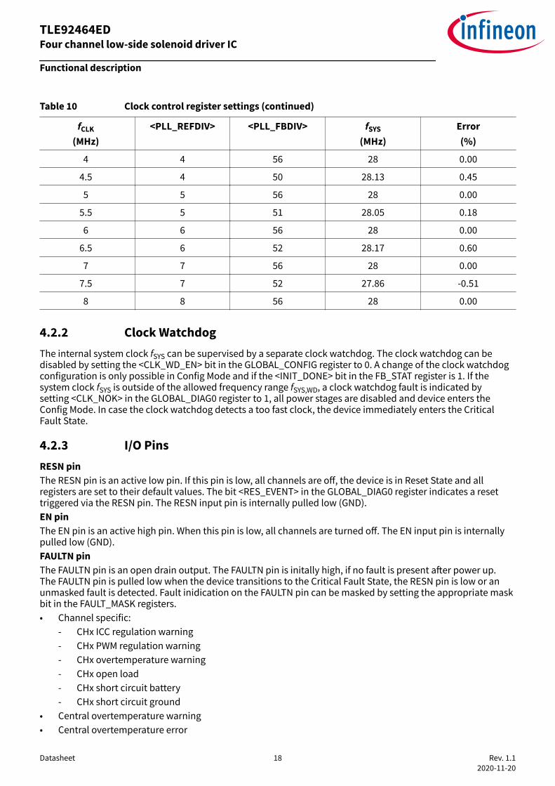
Table 10 Clock control register settings (continued)
fCLK
(MHz)<PLL_REFDIV> <PLL_FBDIV> fSYS
(MHz)Error(%)
4 4 56 28 0.00
4.5 4 50 28.13 0.45
5 5 56 28 0.00
5.5 5 51 28.05 0.18
6 6 56 28 0.00
6.5 6 52 28.17 0.60
7 7 56 28 0.00
7.5 7 52 27.86 -0.51
8 8 56 28 0.00
4.2.2 Clock WatchdogThe internal system clock fSYS can be supervised by a separate clock watchdog. The clock watchdog can bedisabled by setting the <CLK_WD_EN> bit in the GLOBAL_CONFIG register to 0. A change of the clock watchdogconfiguration is only possible in Config Mode and if the <INIT_DONE> bit in the FB_STAT register is 1. If thesystem clock fSYS is outside of the allowed frequency range fSYS,WD, a clock watchdog fault is indicated bysetting <CLK_NOK> in the GLOBAL_DIAG0 register to 1, all power stages are disabled and device enters theConfig Mode. In case the clock watchdog detects a too fast clock, the device immediately enters the CriticalFault State.
4.2.3 I/O PinsRESN pinThe RESN pin is an active low pin. If this pin is low, all channels are off, the device is in Reset State and allregisters are set to their default values. The bit <RES_EVENT> in the GLOBAL_DIAG0 register indicates a resettriggered via the RESN pin. The RESN input pin is internally pulled low (GND).EN pinThe EN pin is an active high pin. When this pin is low, all channels are turned off. The EN input pin is internallypulled low (GND).FAULTN pinThe FAULTN pin is an open drain output. The FAULTN pin is initally high, if no fault is present after power up.The FAULTN pin is pulled low when the device transitions to the Critical Fault State, the RESN pin is low or anunmasked fault is detected. Fault inidication on the FAULTN pin can be masked by setting the appropriate maskbit in the FAULT_MASK registers.• Channel specific:
- CHx ICC regulation warning- CHx PWM regulation warning- CHx overtemperature warning- CHx open load- CHx short circuit battery- CHx short circuit ground
• Central overtemperature warning• Central overtemperature error
Functional description
Datasheet 18 Rev. 1.12020-11-20
TLE92464ED Four channel low-side solenoid driver IC

• SPI watchdog error• Clock too slow error• Data error• EN pin status indication• Internal/External supply faultCLK pinA digital input clock signal fCLK must be applied on the CLK pin if an external clock input is used. Using theinternal clock, the pin should be connected to GND. The CLK input pin is internally pulled low (GND).DRV pinsThe DRV pins enable a direct control of the output stages, if the channel is configured to Direct Drive Mode viaDRV pin. The DRV input pins are internally pulled low (GND). Unused DRV pins should be connected to GND.SI, SO, CSN, SCK pinThe SI, SO, CSN, and SCK pins comprise the SPI interface. See SPI chapter for details.
4.2.4 Electrical characteristics I/O
4.2.4.1 Control inputs EN, RESN, CLK, DRVx
Table 11 Control inputs EN, RESN, CLK, DRVxTJ = -40°C to 150°C; VDD = 4.5 - 5.5 V; VIO = 3.0 - 5.5 V; VBAT = 6 - 18 V; all voltages with respect to ground, positivecurrent flowing into pin (unless otherwise specified).
Parameter Symbol Values Unit Note or conditionMin. Typ. Max.
Digital highthresholdvoltage (EN,RESN, CLK,DRVx)
VEN,highVRESN,highVCLK,highVDRVx,high
2 – - V
Digital lowthresholdvoltage (EN,RESN, CLK,DRVx)
VEN,lowVRESN,lowVCLK,lowVDRVx,low
- – 0.8 V
Digital inputhysteresis (EN,RESN, CLK,DRVx)
VIN_HYS,ENVIN_HYS,RESNVIN_HYS,CLKVIN_HYS,DRVx
- 50 - mV
Pull downcurrent (EN,RESN, CLK,DRVx)
IPD,ENIPD,RESNIPD,CLKIPD,DRVx
10 – 50 µA VIN = 0.8 V
Functional description
Datasheet 19 Rev. 1.12020-11-20
TLE92464ED Four channel low-side solenoid driver IC

4.2.4.2 FAULTN
Table 12 FAULTNTJ = -40°C to 150°C; VDD = 4.5 - 5.5 V; VIO = 3.0 - 5.5 V; VBAT = 6 - 18 V; all voltages with respect to ground,positive current flowing into pin (unless otherwise specified).
Parameter Symbol Values Unit Note or conditionMin. Typ. Max.
Output lowthresholdvoltage(FAULTN)
VFAULTN,LOW 0 – 0.4 V IFAULTN = 2 mA
Output leakagecurrent(FAULTN)
IFAULTN,LGK -100 – 100 µA No fault present 0 V < VFAULTN < VIO
Functional description
Datasheet 20 Rev. 1.12020-11-20
TLE92464ED Four channel low-side solenoid driver IC

4.3 IC Operation statesReset state:• The answer to an SPI command is the 16 bit reply frame.• All SPI register values are being reset to default when the product leaves the Reset State.Config Mode: • All channels are disabled. <EN_CH> bits are 0 and cannot be set.• Channel diagnostic is disabled (HS and LS current source are disabled).• The Channel Mode, the global configuration, the parallel channel operation and the PLL divider can only be
configured in Config Mode.Mission Mode:• The channels and their respective diagnosis are only functional in Mission Mode.Critical Fault state:• The IC will reply all SPI interactions with the Critical Fault frame.• The FAULTN pin is pulled low. The following State Diagram gives an overview on the transition conditions.
Functional description
Datasheet 21 Rev. 1.12020-11-20
TLE92464ED Four channel low-side solenoid driver IC

0RESETstate
1ConfigMode
2MissionMode
OR-Condition1)POR
RESN pin = low
OR-Condition1)POR
RESN pin = low
3Critical Fault
State
OR-Condition1)POR
RESN pin = low
clock too fast fault
clock too fast fault
1): POR: power on reset2): Clock too slow fault detected
1)POROR
RESN pin = low
AND-ConditionFB_STAT register:
INIT_DONE=1GLOBAL_DIAG0:SPI_WD_ERR = 0
CLK_NOK = 0<VIO_UV/OV> = 0<VDD_UV/OV> = 0<VBAT_UV/OV> = 0
<COTW/Ex> = 0GLOBAL_DIAG1:
<VDD2V5_UV/OV> = 0<REF_UV/OV> = 0
<VR_IREF_UV/OV> = 0<REG_ECC_ERR> = 0DIAG_ERR_CHGR0/1:
<OTW/Ex> = 0CH_CTRL:
OP_MODE = 1
OR-ConditionGLOBAL_DIAG0:SPI_WD_ERR = 1
2)CLK_NOK = 1<VIO_UV/OV> = 1<VDD_UV/OV> = 1GLOBAL_DIAG1:
<VDD2V5_UV/OV> = 1<REF_UV/OV> = 1
<VR_IREF_UV/OV> = 1<REG_ECC_ERR> = 1
CH_CTRL:OP_MODE = 0
AND-ConditionNo clock too fast fault
Supply okRESN pin = highclock too fast fault
Figure 4 Operation States and Transitions
Functional description
Datasheet 22 Rev. 1.12020-11-20
TLE92464ED Four channel low-side solenoid driver IC

4.4 Channel modesThe IC offers different modes to control the output stage of a channel. The channel mode can be selectedby programming the MODE register. A change of the channel mode is only possible in Config Mode. Themeasurment period Tmeas for averaged feedback values depends on the selected channel mode (see chapter"current supervision").
Channel Mode Measurement Period Tmeas for Feedback Values
Channel off No measurement active
Current Control ICC Dither Period TDither
Direct Drive via on-time (TON register) Dither Period TDither
Direct Drive via DRV pin • If configured Dither Period TDither, else• Time between two rising edges at DRV pin
Measurement Mode* Dither Period TDither
Note: The current measurement over the shunt can be used for high-precision current measurementapplications. In measurement mode the internal low-side switch is non-conductive.
Note: For more details on the "Current Control" and "Direct Drive" Mode please refer to the respectivechapters.
Functional description
Datasheet 23 Rev. 1.12020-11-20
TLE92464ED Four channel low-side solenoid driver IC
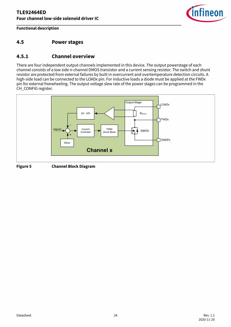
4.5 Power stages
4.5.1 Channel overviewThere are four independent output channels implemented in this device. The output powerstage of eachchannel consists of a low side n-channel DMOS transistor and a current sensing resistor. The switch and shuntresistor are protected from external failures by built in overcurrent and overtemperature detection circuits. Ahigh-side load can be connected to the LOADx pin. For inductive loads a diode must be applied at the FWDxpin for external freewheeling. The output voltage slew rate of the power stages can be programmed in theCH_CONFIG register.
Output-Stage
Current Controller
PWMDriver Block
ΔΣ - A/D
-setpoint
Channel x
FWDx
GNDPx
DMOS
RShunt
Dither
+
LOADx
Figure 5 Channel Block Diagram
Functional description
Datasheet 24 Rev. 1.12020-11-20
TLE92464ED Four channel low-side solenoid driver IC

4.5.2 Parallel channel operationThe IC features a parallel mode of output stages to increase the maximum current capability of the device.The channels 0 and 3 and the channels 1 and 2 can be connected in parallel. Channel 0 and 1 are the masterchannels and channel 2 and 3 are the slave channels. Only the master channels can be configured via SPI. Theparallel channel mode can be enabled or disabled in the CH_CTRL register when the device is in Config Mode.
VBAT
Current Controller
<x>
PWMDriver Block
<x>
ΔΣ - A/D <y>
ΔΣ - A/D<x>
-
+
setpoint
PWMDriver Block
<y>
Lload
D
Parallel Channel
LOAD<x>
FWD<x>
LOAD<y>
FWD<y>
GNDP<y>
GNDP<x>
DMOS<y>
DMOS<x>
RShunt
<x>
RShunt
<y>
Dither<x>
+
-
Iloadx,y,par
Figure 6 Parallel Channel Configuration
Slave channelThe current controller and the OFF-state diagnosis of the slave channel are disabled. A write access to the MODEregister of the slave channel is ignored and reads back zero. The slave channel´s SETPOINT register cannot beset and is read back as zero. All feedback registers of the slave channel have to be disregarded. A write to a slave<EN_CH> bit is ignored and 0 is read back. After disabling the parallel channel mode the slave channel must bere-configured to the desired channel behaviour.SetpointIn parallel channel mode, the programmed setpoint of the master channel is used. Hence the LSB (leastsignificant bit) of the setpoint is doubled.Diagnostic functionsThe LSB of the fixed OLSG (open load/short to GND) threshold is scaled by a factor of two. The OC (overcurrent)protection feature is active on the master as well as on the slave channel. If either the master or the slavechannel detects an OC fault, both channels are disabled.Feedback functionsThe current feedback in the FB_I_AVG register represent the summed up current over the shunt resistors of themaster and slave channel. The duty cycle feedback can be read from the master channel.
Functional description
Datasheet 25 Rev. 1.12020-11-20
TLE92464ED Four channel low-side solenoid driver IC

4.5.3 Electrical characteristics power stages
Table 13 Electrical characteristics power stagesTJ = -40°C to 150°C; VDD = 4.5 - 5.5 V; VIO = 3.0 - 5.5 V; VBAT = 6 - 18 V; all voltages with respect to ground, positivecurrent flowing into pin (unless otherwise specified).
Parameter Symbol Values Unit Note or conditionMin. Typ. Max.
Shuntresistance
Rshunt – 140 185 mΩ
ON resistance RDSON - 115 2001) mΩ 1) TJ = 150°C, ILOADx = 2.0 A
Leakagecurrent(LOADx, FWDx)
ILOADx,LKG IFWDx,LKG
-100 – 100 µA VBAT = 18 V; Setpoint = 0 mA; Diagnosis off
Slew rate 0 SR0 0.5 1 2 V/µs VBAT=14V; RLOAD=10Ω20% to 80% of applied load voltage<SLEWR> = 00B
Slew rate 1 SR1 1.25 2.5 5 V/µs VBAT=14V; RLOAD=10Ω20% to 80% of applied load voltage<SLEWR> = 01B
Slew rate 2 SR2 2.5 5 10 V/µs VBAT=14V; RLOAD=10Ω20% to 80% of applied load voltage<SLEWR> = 10B
Slew rate 3 SR3 5 10 20 V/µs VBAT=14V; RLOAD=10Ω20% to 80% of applied load voltage<SLEWR> = 11B
Functional description
Datasheet 26 Rev. 1.12020-11-20
TLE92464ED Four channel low-side solenoid driver IC
4.6 Current control
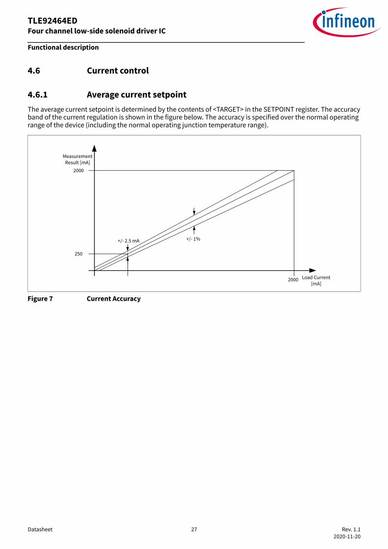
4.6.1 Average current setpointThe average current setpoint is determined by the contents of <TARGET> in the SETPOINT register. The accuracyband of the current regulation is shown in the figure below. The accuracy is specified over the normal operatingrange of the device (including the normal operating junction temperature range).
Measurement Result [mA]
2000
250
+/- 1%+/- 2.5 mA
Load Current [mA]
2000
Figure 7 Current Accuracy
Functional description
Datasheet 27 Rev. 1.12020-11-20
TLE92464ED Four channel low-side solenoid driver IC

4.6.2 Integrating Current Controller (ICC)The current controller regulates the load current automatically to a user defined setpoint by turning on andoff the internal transistor. If the internal transistor is switched on, the current through the inductive load willincrease. If the internal transistor is turned off, the current will continue to flow through the recirculation diodegradually decay.The Integrating Current Controller (ICC) is based on the requirement that the integrated current error overone PWM cycle is zero. This means that the average current after one PWM cycle exactly equals the targetedcurrent. The controller integrates the current deviation (difference between load current and the setpoint)and switches the output stage accordingly: While the integrated current deviation is below a configurableintegrator threshold, the power stage is turned on. In this phase the load current will increase. When theintegrated current error exceeds the determined integrator threshold the power stage is turned off and thecurrent recirculates through the freewheeling diode. The average current is reached when the integratedcurrent deviation crosses zero which determines the start of a new PWM cycle. The ICC switching characteristicprovides the physically fastest current response which makes it very robust against load voltage dips.
“on time” “off time”
I setpoint
Output Stage State
Error Integrator threshold
Load Current
Figure 8 Current Control Waveform
Functional description
Datasheet 28 Rev. 1.12020-11-20
TLE92464ED Four channel low-side solenoid driver IC

4.6.2.1 Integrator limitsThe ICC integrator can be saturated in order to avoid an integrator windup. The integrator limits areconfigurable via +/-<LIM_VALUE_ABS> in the INTEGRATOR_LIMIT register.In order to avoid current overshoots after setpoint changes the Autolimit feature is introduced. The devicelimits the integrator value to +/-<AUTO_LIM_VALUE_ABS> (INTEGRATOR_LIMIT register) for a maximum of twoPWM cycles after a setpoint change. After the completion of Autolimit, the ICC automatically revert back tothe normal integrator limit values +/-<LIM_VALUE_ABS>. The Autolimit feature is disabled by writing a 1 to the<AUTO_LIMIT_DIS> bit in the SETPOINT register.
ò (i(t)-iset)dt
i(t)
t
t
+ <AUTO_LIM_VALUE_ABS>
setpoint
Autolimit
- <AUTO_LIM_VALUE_ABS>
Figure 9 Autolimit feature
Functional description
Datasheet 29 Rev. 1.12020-11-20
TLE92464ED Four channel low-side solenoid driver IC

4.6.2.2 PWM frequency controlThe load characteristic and load supply voltage affecting the PWM output frequency of the ICC controller. Theon-time of the LS-FET and therefore the PWM cycle can be adjusted by modifying the integrator thresholdvalue. A greater integrator threshold ends up in a longer on-time. Although the configured integrator thresholdvalue is positive, the actual threshold can get negative since it is referenced to the lowest current deviationintegral value captured during the on-phase. This means very short on-time configurations are possible.The shortest on-time is determined by limiting the integrator threshold to a minimum value configurablevia <MIN_INT_THRESH> in the CTRL register.There are two options to set the integrator threshold to adjust the PWM frequency.Manual setting of On-timeThe driver on-time and therefore a target PWM period can be set manually by programming a fixed integratorthreshold <INT_THRESH> in the CTRL_INT_THRESH register. The PWM frequency controller has to be disabledby setting <PERIOD_MANT> in the PERIOD register to 0.Automatic PWM controlThe PWM frequency controller regulates the PWM frequency using an “Integral” control loop with aprogrammable gain, KI. This control loop monitors the actual PWM period and compares substracts it fromthe PWM period target setting in the PWM period register. The error in the PWM period is multiplied by the gainKI and then integrated at each PWM cycle. The output of the controller adjusts the on-time of the PWM signaluntil the actual PWM period matches the programmed PWM period. The internal PWM frequency controller canbe activated by setting a target PWM period Tperiod in the PERIOD register.
Tperiod = < PERIOD_MANT > · 2< PERIOD_EXP >fSYSEquation 4
By setting the bit <LOW_FREQ_RANGE_EN> the range of the configurable target PWM frequency is lower andcan be calculated as follow.
Tperiod = < PERIOD_MANT > · 8 · 2< PERIOD_EXP >fSYSEquation 5
The bitfield <INT_THRESH> in the CTRL_INT_THRESH register determines the integrator threshold used aftersetpoint changes or activation of the PWM controller. The <INT_THRESH> value must be configured beforeapplying the new setpoint. The resulting threshold calculated by the PWM frequency controller can be retrievedfrom the FB_INT_THRESH register. The threshold calculated by the PWM frequency controller can be read backfrom the FB_INT_THRESH register. The threshold value can be used to program <INT_THRESH> to reduce thesettling time of the PWM frequency controller e.g. after a setpoint change.Note: The Autolimit threshold must be greater than the lower threshold limit configuration for a correct ICCfunctioning (<AUTO_LIM_VALUE_ABS> > <MIN_INT_THRESH>+0x3).The PWM frequency control parameter KI can be set by <PWM_CTRL_PARAM> in the PERIOD register. Theintegrator parameter KI determines the gain and therefore the speed of the PWM frequency control loop. A KIvalue of 0 results in a slower but more stable PWM control.During steep dither settings, long off-times can appear which end up in high frequencies in the nextrising dither slope. The frequency controller does not consider falling dither slopes by setting the<PWM_PERIOD_CALC_MODE> in the CTRL register.
Functional description
Datasheet 30 Rev. 1.12020-11-20
TLE92464ED Four channel low-side solenoid driver IC

4.6.2.3 PWM regulation warningAn ICC PWM regulation warning is issued if the ICC integrator value drops below the minimum integral value,which was captured during the on-phase. This can happen i.e. if a negative absolute integrator threshold iscalculated from the PWM control and the inertia of the load is too large. This means the integrated currentdeviation could not exceed the zero level and therefore the power stage would not switch on anymore.A negative integrator threshold can be avoided by programming <MIN_INT_THRESH> in the CTRL register to avalue greater than 1. A recovery process maintains the current regulation by triggering the Autolimit feature.After finishing Autolimit, the integrator threshold configured in <INT_THRESH> bitfield is used. The PWMregulation warning is signaled by asserting the <PWM_REG_WARN> bit in the DIAG_WARN_CHGR register.
<AUTO_LIM_VALUE_ABS>
t
ò (i(t)-iset)dt
- <AUTO_LIM_VALUE_ABS>minimum
mar
gin
PWM regulation warning
<int_thresh>
Integrator threshold of PWM control
Autolimit active
t
i(t)
Figure 10 ICC PWM regulation warning
Functional description
Datasheet 31 Rev. 1.12020-11-20
TLE92464ED Four channel low-side solenoid driver IC

4.6.2.4 Current regulation warningAn ICC current regulation warning occurs if the ICC integrator value reaches the absolute integrator limit<LIM_VALUE_ABS> located in the INTEGRATOR_LIMIT register. This can happen for example during a voltagesupply dip. A recovery process maintains the current regulation by triggering the Autolimit feature. Theintegrator threshold will be reset to <INT_THRESH> located in the CTRL_INT_THRESH register. The warningis signaled by asserting the respective <I_REG_WARN> bit in the DIAG_WARN_CHGR register.
<AUTO_LIM_VALUE_ABS>
t
ò (i(t)-iset)dt
- <AUTO_LIM_VALUE_ABS>Autolimit active
t
i(t)
- <LIM_VALUE_ABS>
low solenoid supply
current regulation warning
Figure 11 ICC current regulation warning
Functional description
Datasheet 32 Rev. 1.12020-11-20
TLE92464ED Four channel low-side solenoid driver IC

4.6.3 Electrical characteristics current control
Table 14 Electrical characteristics current controlTJ = -40°C to 150°C; VDD = 4.5 - 5.5 V; VIO = 3.0 - 5.5 V; VBAT = 6 - 18 V; all voltages with respect to ground, positivecurrent flowing into pin (unless otherwise specified).
Parameter Symbol Values Unit Note or conditionMin. Typ. Max.
Averagecurrent controlerror, absolut
Ierr.absolut -2.5 – 2.5 mA Iset = 10 - 250mASingle channel operation
Averagecurrent controlerror, absolut -parallel
Ierr.absolut,par -5 - 5 mA Iset,par = 20 - 500 mAParallel channel operation
Averagecurrent controlerror, relative
Ierr.relative -1 – 1 % Iset > 250mA; single channel operationIset,par > 500mA; parallel channel operation
Load current Iset 0 – 1500 mA DC setpoint current Single channel operation
Dither current Iset+ IDither 0 – 1800 mA DC setpoint current incl. dither currentamplitudeSingle channel operation
Measurementcurrent
ILOADx 0 – 2000 mA DC setpoint incl. dither current amplitude andovershootSingle channel operationThe user must take care that the maximumvalue is not exceeded
Measurementcurrent -parallel
ILOADx,y,par 0 - 2700 mA DC setpoint current incl. dither currentamplitude and overshootParallel channel operationSingle channel measurement range ILOADx ofeach Channel shall not be violated
Functional description
Datasheet 33 Rev. 1.12020-11-20
TLE92464ED Four channel low-side solenoid driver IC

4.7 Dither
4.7.1 Dither configurationA configurable dither waveform can be added to the average current setpoint in order to reduce the hysteresisof a driven solenoid valve. The dither operation is an overlay of a triangular or trapezoidal waveform over thecurrent setpoint. The dither waveform is generated by permanently changing the setpoint according to theprogrammed shape.The dither shape can be configured by setting the <STEPS>, <STEP_SIZE> and <FLAT> values in theDITHER_STEP and DITHER_CTRL register. The <STEP_SIZE> value scales the height of each dither step wherethe LSB is equal to <TARGET> in the setpoint register. The value of <STEPS> determines the number of stepsfor the rising and falling edge of each half cycle of the dither waveform. The value of <FLAT> determines thenumber of flat steps at the minimum and maximum plateau of the dither waveform.The amplitude of the dither waveform overlay IDither can be calculated as follows.
IDitℎer = < STEPS > · < STEP_SIZE > · 2A215 − 1
Equation 6
Care should be taken that no negative dither amplitude (Iset - IDither > 0) is configured and possible overshootsare not violating the specified measurement current range ILOADx or ILOADx,par (parallel channel operation). Thedither overlay IDither is deactivated if the target setpoint is set to 0.The Dither period TDither is a muliple of the Dither reference clock determined by the values of <MANT>, <EXP>of the DITHER_CLK_DIV register. The dither period TDither and dither reference clock tref_clk can be calculated asfollows.
TDitℎer = 4 · < STEPS > + 2 · < FLAT > · tref_clkEquation 7
tref_clk = < MANT > · 2< EXP >fSYSEquation 8
tflat = < FLAT > · tref_clkEquation 9
Note: If <STEPS> = 0 and <FLAT> = 0, the dither period TDither = tref_clk
Functional description
Datasheet 34 Rev. 1.12020-11-20
TLE92464ED Four channel low-side solenoid driver IC

dither amplitude IDither
dither period TDither
<STEPS> = 4 <FLAT> = 3
<STEP_SIZE> setpoint Iset
Figure 12 Dither Waveform Configuration
4.7.2 Dither parameter updateAll dither parameters located in registers DITHER_STEP and DITHER_CTRL become active at the start ofthe next dither period after writing to the DITHER_CTRL register. After triggering an update event (writeto DITHER_CTRL) within the active dither period, the dither configuration ( DITHER_STEP/ DITHER_CTRL)that was transmitted last within the active dither period is taken over. An update of the reference clocktref_clk controlled by the DITHER_CLK_DIV register takes immediate effect. If the dither amplitude is disabled byclearing <STEP_SIZE>, the active dither period will be completed. The configured dither period and overlay isimmediately (re)-started if the <EN_CH> bit transitions to 1.
4.7.3 Dither PWM SynchronizationThe dither-PWM synchronization starts a new dither period synchron with the start of the next PWM cycle toenable the same starting conditions for each dither period. The start of a PWM cycle period is defined as a turnon of the output stage. The start of a dither period is defined to be when the dither increases one step abovezero on this rising slope of the dither waveform. The dither-PWM synchronization can be enabled by setting the<DITHER_PWM_SYNC_EN> bit in the DITHER_CLK_DIV register. When the <DITHER_PWM_SYNC_EN> bit is set to0, the dither waveform is free-running and asynchronous to the PWM frequency.
Functional description
Datasheet 35 Rev. 1.12020-11-20
TLE92464ED Four channel low-side solenoid driver IC

SYNC = 0 : Dither period is independent of switching cycle periodSYNC = 1 : Start of dither period is delayed until start of next switching cycle period
Load Current without SYNC
Load Current with SYNCSetpoint + Dither shape with SYNC
SYNC occurs
Setpoint + Dither shape without SYNC
Current_Control_Dither_Sync.vsdx
Figure 13 Dither sync
Note: This feature is only available in ICC Channel Mode.
Functional description
Datasheet 36 Rev. 1.12020-11-20
TLE92464ED Four channel low-side solenoid driver IC

4.7.4 Dither Setpoint SynchronizationThe dither-setpoint synchronization feature updates the averaged feedback values of a channel (FB_DC,FB_I_AVG, FB_VBAT) after a change in setpoint in the shortest possible time. The dither-setpointsynchronization restarts the dither period when the newly applied setpoint has been reached. Therefore, themeasurement period Tmeas (dither period) for the feedback values is always in lockstep with a setpoint changeand no latency of the averaged feedback values (FB_DC, FB_I_AVG, FB_VBAT) is present. The synchronizationof the dither period to a setpoint change can be enabled by programming the <DITHER_SETPOINT_SYNC_EN>bit in the DITHER_CLK_DIV register. An enabled setpoint synchronization freezes the average feedback registers(FB_DC, FB_I_AVG, FB_VBAT) with the last valid measurement result if the channel is disabled with setpoint "0".
Note: This feature is only available in ICC Channel Mode.
4.7.5 Deep ditherA steep and deep dither command is comparable to great changes of setpoint. The deep dither function reducesthe over- and undershoot of very steep dither overlays by permanently enabling the Autolimit feature. The deepdither feature can be enabled by setting the <DEEP_DITHER> bit in DITHER_CTRL register.
Note: This feature is only available in ICC Channel Mode.
4.8 Direct DriveIn Direct Drive, the channel's output stage is controlled directly by the user. To enable a output stage switching,the respective channel must be activated by setting <EN_CH> bit to 1 and a target current setpoint valuedifferent to zero. The Direct Drive mode must be selected by programming the MODE register.Direct Drive mode via DRV pinIn Direct Drive mode via DRV pin the channel’s output stage is switched according to the logic level at thecorresponding DRV pin. The channel is turned on if the DRV pin is high and is switched off if the DRV pin is low.Direct Drive mode via SPI on-TimeIn Direct Drive mode via SPI on-Time, the channel’s output stage is switched according to a configurable period.The period Tperiod is set in the DITHER_CLK_DIV register by the bit fields <MANT> and <EXP>. The on-time tonduring a period can be configured with the <TON_MANT> bit field in the TON register.
Tperiod = < MANT > · 2< EXP >fSYSton = < TON_MANT > · 2< EXP >fSYSEquation 10
Functional description
Datasheet 37 Rev. 1.12020-11-20
TLE92464ED Four channel low-side solenoid driver IC

4.9 Diagnostic functions
4.9.1 OverviewEach IC channel has an independend open load (OL), overcurrent (OC) and short circuit to ground (SG)diagnosis.The following points should be considered:• All failure modes are only considered to occur on the off board routed LOAD-pin.• The diagnosis indication bits are clear on write.• The diagnosis is only enabled if the device is in Mission ModeThe diagnosis consists of an ON-state diagnosis and an OFF-state diagnosis. Both diagnosis states shall be usedto enable a full fault analysis coverage.ON-state diagnosisA channel is in ON-state if the <EN_CH> bit is set and the setpoint value is different to 0 mA. All diagnosticfunctions in ON-state rely on measuring the current through the shunt resistor. The ON-state diagnosis cannotdistinguish between a short circuit to ground (SG) and an open load (OL) fault. Those faults are summarized toan Open Load/Short to Ground fault (OLSG) in the ON-state. A distinction whether an OL or SG is present needsto be done by the OFF-state diagnosis.OFF-state diagnosisA channel is in OFF-state if1. the setpoint is 0 and the <EN_CH> bit is set to 1 (EN-pin must be high for use of OFF-state diagnosis state
machine)2. the setpoint is non-zero and the <EN_CH> bit is set to 0.The first condition can be used to initially test the application circuit. The second condition is present after theON-state diagnosis has detected a fault .In OFF-state, the internal high and low side current sources IHS and ILS at the LOADx pin are active. The switchingconfiguration and current strength of IHS and ILS can configured in the CH_CONFIG register.
LOADx
FWDx
RShunt
Load D
VBAT
IHS
ILS
IHS_enable
ILS_enable
OFF-state Diagnosis
GNDPx
C
VBAT
DMOS
Figure 14 OFF-state diagnosis circuit
Setting <OFF_DIAG_CH> bit in the CH_CONFIG register to "0", activates the OFF-state diagnosis. The OFF-statediagnosis detects and indicates open load (OL) or short circuit to ground (SG) faults by performing followingLOAD pin voltage checks.
Functional description
Datasheet 38 Rev. 1.12020-11-20
TLE92464ED Four channel low-side solenoid driver IC

1. The low side diagnostic current ILS is enabled and the high side diagnostic current IHS is disabled.• If VLOAD > VTH_BAT/2 no fault is detected.• If VLOAD < VTH_BAT/2 the sequence continues.
2. The high side diagnostic current IHS is enabled and the low side diagnostic current ILS is disabled.• If VLOAD > VTH_BAT/2 an OL is detected and indicated in the DIAG_ERR_CHGR register.• If VLOAD < VTH_BAT/2 a SG is detected and indicated in the DIAG_ERR_CHGR register.
The OFF-state diagnosis handles all channels sequentially. The OFF-state diagnosis sequence takes Toff,sequence.
CHx in OFF-state
VLOAD < VTH_BAT/2NO
activate IHS
VLOAD < VTH_BAT/2
set OLx
fault bitNO
YESsetSGx
fault bit
activate ILS
wait for CHx handling
settling timeNo
Fault.keep ILS enabled
YES
settling time
Figure 15 OFF-state diagnosis sequence
Functional description
Datasheet 39 Rev. 1.12020-11-20
TLE92464ED Four channel low-side solenoid driver IC

4.9.2 Open Load/Short to Ground (OLSG)An open load (OL) and a short circuit to ground (SG) are both reducing the current flowing through the shuntresistor. Therefore the faults cannot be distinguished in ON-state and are summarized as OLSG fault. An OLSGis detected if the cumulated driver on-time equals TOLSGON and the load current ILOAD is below the open loadthreshold IOLTH.
i (t)
IOLTH
t
Open Load or Short to Ground happened
ton1
No OLSG
ton2
OLSG detectedTOLSGON = ton1 + ton2
Figure 16 Simplified OLSG detection mechanism
An OLSG fault switches off the respective power stage and is indicated by setting the respective OLSG bit in theDIAG_ERR_CHGR register. The device keeps the channel disabled until the fault is removed, the diagnosis bit iscleared and the <EN_CH> bit is set to “1” again.ROLmin is the minimum impedance to detect an OL in ON-state via an OLSG fault.
ROLmin = VBATIOLTH − RLOAD + Rsℎunt + RDSonEquation 11
RSGmax is the maximum impedance to detect an SG in ON-state via an OLSG fault.
RSGmax = RLOAD · Rsℎunt + RDSonROLminEquation 12
Functional description
Datasheet 40 Rev. 1.12020-11-20
TLE92464ED Four channel low-side solenoid driver IC

4.9.2.1 OL - Threshold configurationThe open load threshold IOLTH can be set to a fixed threshold and/or a threshold relative to the setpoint via theCH_CONFIG register. The OLSG diagnosis is disabled by setting both OL-thresholds to 0. Fixed OL-ThresholdA fixed open load threshold is programmable via bitfield <OL_TH_FIXED>.
IOLTH = < OL_TH_FIXED > · 128 · 2000mA215 − 1IOLTH,parallel = < OL_TH_FIXED > · 128 · 4000mA
215 − 1
Equation 13
Note: The OL detection in direct drive mode is only possible with the fixed threshold configuration. Relative OL-ThresholdThe relative threshold refers to the actual setpoint Iset including the dither amplitude IDither. A relative open loadthreshold is adjustable in bitfield <OL_TH>. The relative open load threshold is disabled by setting <OL_TH> to0.
IOLTH = Iset + IDitℎer · < OL_TH >8
Equation 14
Note: The relative threshold is only available in a current control mode. Transition phaseDuring a transition phase, the fixed OL-threshold is always used. A transition phase takes place after a channelactivation or setpoint change. A transition phase lasts for one PWM cycle or maximum for a driver on-time ofTOLSGON (PWM cycle > TOLSGON). The transition phase time out can be extended or shortened by configuringtOLSG_TIMEOUT in the TON register. After the transition phase has been finished, the OLSG detection swaps fromfixed to relative OL-threshold. If the <OL_TH_FIXED> bitfield is set to 0, no OLSG will be detected duringa transition phase.
tOLSG_TIMEOUT = < OLSG_TIMEOUT > · 256 + 255 · 64fSYSEquation 15
Functional description
Datasheet 41 Rev. 1.12020-11-20
TLE92464ED Four channel low-side solenoid driver IC
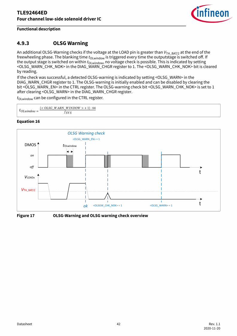
4.9.3 OLSG WarningAn additional OLSG-Warning checks if the voltage at the LOAD pin is greater than VTH_BAT/2 at the end of thefreewheeling phase. The blanking time tOLwindow is triggered every time the outputstage is switched off. Ifthe output stage is switched on within tOLwindow, no voltage check is possible. This is indicated by setting<OLSG_WARN_CHK_NOK> in the DIAG_WARN_CHGR register to 1. The <OLSG_WARN_CHK_NOK> bit is clearedby reading.If the check was successful, a detected OLSG-warning is indicated by setting <OLSG_WARN> in theDIAG_WARN_CHGR register to 1. The OLSG-warning is initially enabled and can be disabled by clearing thebit <OLSG_WARN_EN> in the CTRL register. The OLSG-warning check bit <OLSG_WARN_CHK_NOK> is set to 1after clearing <OLSG_WARN> in the DIAG_WARN_CHGR register. tOLwindow can be configured in the CTRL register.
tOLwindow = < OLSG_WARN_WINDOW > + 1 · 64fSYSEquation 16
t
VLOADx
DMOS
t
on
off
tOLwindow
VTH_BAT/2
OLSG Warning check<OLSG_WARN_EN> = 1
ok <OLSGW_CHK_NOK> = 1 <OLSG_WARN> = 1
Figure 17 OLSG-Warning and OLSG warning check overview
Functional description
Datasheet 42 Rev. 1.12020-11-20
TLE92464ED Four channel low-side solenoid driver IC

4.9.4 Open Load (OL)In ON-state, an open load is indicated via the <OLSG> bit in the DIAG_ERR_CHGR register. The final faultdiscrimination to identify an open load is done by the OFF-state diagnostic. The device indicates the fault bysetting the respective <OL> bit in the DIAG_ERR_CHGR register. The device keeps the channel disabled until thefault is removed, the diagnosis bit is cleared and the <EN_CH> bit is set to “1” again.
LOADx
FWDx
RShunt
Load D
VBAT
IHS
ILS
IHS_enable
ILS_enable
OFF-state Diagnosis
GNDPx
C
DMOS
VBAT
Figure 18 Open load
Functional description
Datasheet 43 Rev. 1.12020-11-20
TLE92464ED Four channel low-side solenoid driver IC

4.9.5 Short circuit ground (SG)In the ON-state, a short circuit to ground is detected via the <OLSG> bit in the DIAG_ERR_CHGR register. Thefinal fault discrimination to identify a short circuit to ground is done by the OFF-state diagnostic. The deviceindicates the fault by setting the respective <SG> bit in the DIAG_ERR_CHGR register. The device keeps thechannel disabled until the fault is removed, the diagnosis bit is cleared and the <EN_CH> bit is set to “1” again.
LOADx
FWDx
RShunt
Load D
VBAT
IHS
ILS
IHS_enable
ILS_enable
OFF-state Diagnosis
GNDPx
C
RSG
DMOS
VBAT
Figure 19 Short to Ground
Functional description
Datasheet 44 Rev. 1.12020-11-20
TLE92464ED Four channel low-side solenoid driver IC

4.9.6 Overcurrent (OC)An overcurrent fault (OC) is an unintended low impedance connection between the LOAD terminal and thebattery rail, therefore bypassing the load impedance.An overcurrent is detected if a current flow through the power stage exceeds IOC. Therefore the power stagemust be turned on for a short period of time tOCon to detect an OC in OFF-state. The driver on-time tOCon canbe triggered by setting the <OC_DIAG_EN> bit in the CH_CONFIG register and the respective <EN_CH> bit in theCH_CTRL register to 1. The driver on-time tOCon must be configured before executing the OC detection.
tOCon = < TON_MANT > + 1 · 2< EXP >fSYSEquation 17
The mantissa <TON_MANT> is located in the TON register and the exponent <EXP> is located inDITHER_CLK_DIV. An enabled OFF-state diagnosis is kept active during tOCon.<OC_DIAG_EN> is reset after tOCon has expired. If an overcurrent is present, the <EN_CH> bit is cleared andthe indication bit <OC> in the DIAG_ERR_CHGR register is set to 1. The device keeps the channel disabled untilthe fault is removed, the diagnosis bits are cleared by two clear commands and the <EN_CH> bit is set to “1”again.
LOADx
FWDx
RShunt
Load D
VBAT
IHS
ILS
IHS_enable
ILS_enable
OFF-state Diagnosis
GNDPx
C
ROC
DMOS
VBAT
Figure 20 Overcurrent
4.9.7 Register/OTP ECCA register/OTP (one time programmable memory) error or warning will be detected by a continuouserror checking and correction (ECC) mechanism. A register/OTP warning is indicated by settingthe <REG_ECC_WARN>/<OTP_ECC_WARN> bit in the GLOBAL_DIAG2 register. Furthermore, a registerwarning indicates a correction of corrupt data. If a correction is not possible, a register/OTP ECC error is presentand the <REG_ECC_ERR>/<OTP_ECC_ERR> bit in the GLOBAL_DIAG2 register will be set. The <OTP_ECC_ERR>can only be cleared by sending two clear commands. A register ECC error disables all power stages and theproduct enters the Operation State "Config Mode". The <OTP_VIRGIN> bit in the GLOBAL_DIAG2 indicates a nonprogrammed OTP-memory. This bit must always be 0.
Functional description
Datasheet 45 Rev. 1.12020-11-20
TLE92464ED Four channel low-side solenoid driver IC

4.9.8 Built in Self Test (BIST)The device provides a self-test in order to check the built in error detection and correction feature for safetycritical registers. The BIST tests the ability to detect correctable and uncorrectable errors. The BIST canonly be triggered in Config Mode by writing a '1' to the <SMU_SLF_TST_EN> bit in the SFF_BIST register.After the safety flip-flop BIST sequence is completed, the bits <SMU_SLF_TST_DONE>, <SMU_SLF_TST_UERR>and <SMU_SLF_TST_CERR> are set to indicate a finished test sequence.The safety flip-flop BIST result is stored in the <SMU_SLF_TST_FAIL> bit in SFF_BIST register. All resultand status bits in the SFF_BIST register are cleared on writing 0. A successfully tested safety flip-floperror (uncorrectable fault) or warning (correctable fault) sets the respective error bits <REG_ECC_ERR> or<REG_ECC_WARN> in the GLOBAL_DIAG2 register.
Functional description
Datasheet 46 Rev. 1.12020-11-20
TLE92464ED Four channel low-side solenoid driver IC
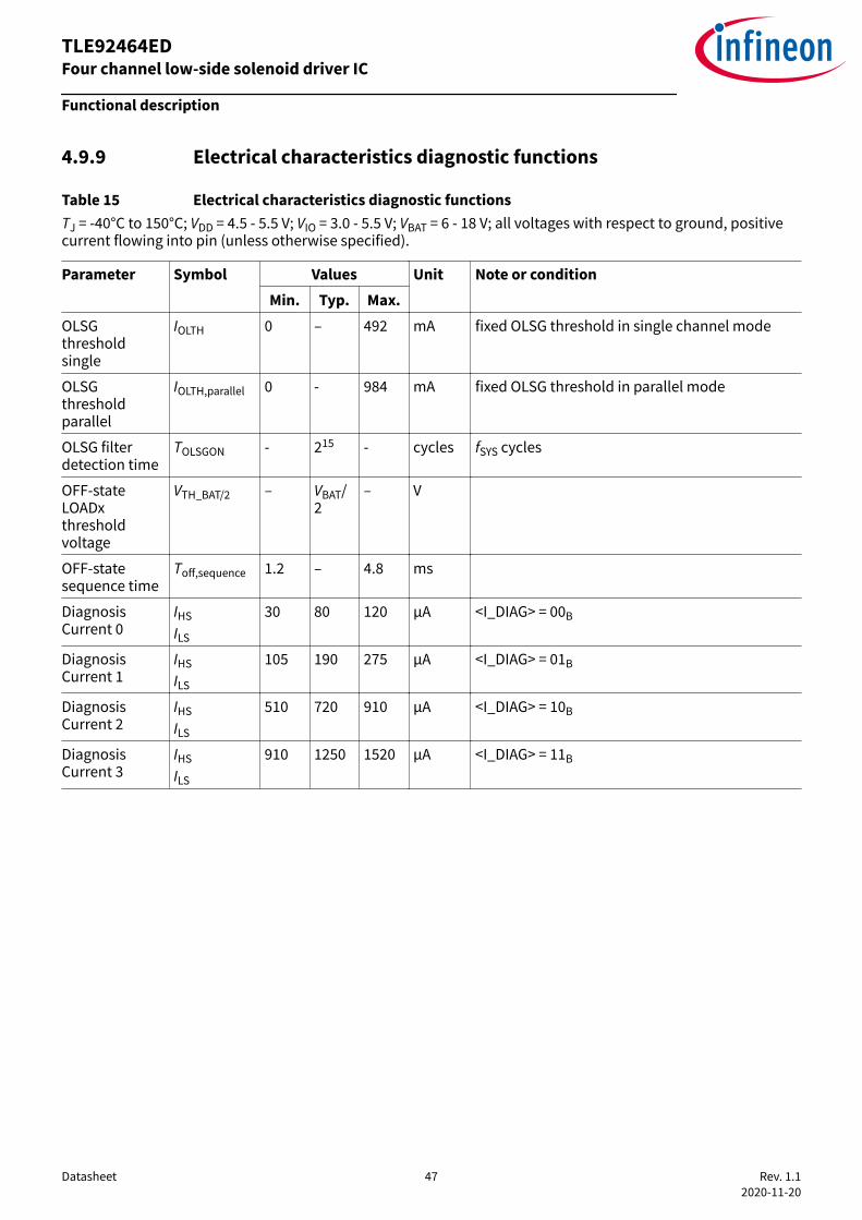
4.9.9 Electrical characteristics diagnostic functions
Table 15 Electrical characteristics diagnostic functionsTJ = -40°C to 150°C; VDD = 4.5 - 5.5 V; VIO = 3.0 - 5.5 V; VBAT = 6 - 18 V; all voltages with respect to ground, positivecurrent flowing into pin (unless otherwise specified).
Parameter Symbol Values Unit Note or conditionMin. Typ. Max.
OLSGthresholdsingle
IOLTH 0 – 492 mA fixed OLSG threshold in single channel mode
OLSGthresholdparallel
IOLTH,parallel 0 - 984 mA fixed OLSG threshold in parallel mode
OLSG filterdetection time
TOLSGON - 215 - cycles fSYS cycles
OFF-stateLOADxthresholdvoltage
VTH_BAT/2 – VBAT/2
– V
OFF-statesequence time
Toff,sequence 1.2 – 4.8 ms
DiagnosisCurrent 0
IHSILS
30 80 120 µA <I_DIAG> = 00B
DiagnosisCurrent 1
IHSILS
105 190 275 µA <I_DIAG> = 01B
DiagnosisCurrent 2
IHSILS
510 720 910 µA <I_DIAG> = 10B
DiagnosisCurrent 3
IHSILS
910 1250 1520 µA <I_DIAG> = 11B
Functional description
Datasheet 47 Rev. 1.12020-11-20
TLE92464ED Four channel low-side solenoid driver IC

4.10 Current supervision
4.10.1 Independent current feedbackThe device provides independent current feedback paths to the microcontroller for plausibility checks onthe load current. The average load current measured via the internal shunt can be read back directly. Theindependently measured duty cycle and battery voltage can be used to calculate the average load current usinga load model.
Current Control +
Dither -
Solenoid Model or
LUT-
error2
Imeas
Duty Cycle
<setpoint>calculated Iaverage
µC
PWMDriver Block
Average
LOAD
FWDRShunt
Load
D
ΔΣ - A/D
VBAT
DMOS
Average
<FB_VBAT_CHx> <FB_DC_CHx>
PWMFeedback
GNDP
-
error1
VBAT
Battery Voltage
Solenoid Driver IC
Average Current<FB_I_AVG_CHx>
Average
Figure 21 Current supervision
Functional description
Datasheet 48 Rev. 1.12020-11-20
TLE92464ED Four channel low-side solenoid driver IC

4.10.2 Average feedback valuesThe feedback values are provided in the registers FB_DC, FB_VBAT, FB_I_AVG. The feedback values averagedover the configured measurement period Tmeas (see "Channel modes"). The register contents are updated aftereach measurement period Tmeas.The feedback values can be calculated as follows:• Measurement period:
Tmeas = < TP_MANT > · 2< EXP >fSYSEquation 18
• PWM on time:
ton = < TO_MANT > · 2< EXP >fSYSEquation 19
• Duty cycle:
DC = < TO_MANT >< TP_MANT >Equation 20
• Battery voltage:
VBAT = 41 . 47V · < VBAT_AVG_MANT >< TP_MANT >Equation 21
• Average load current (signed):
Iavg = 4A · < I_AVG_MANT >< TP_MANT >Equation 22
The bitfields <TP_MANT> and <TO_MANT> are located in the FB_DC register. The bitfields <VBAT_AVG_MANT>and <EXP> are loacated the FB_VBAT register. The bitfield <I_AVG_MANT> is located in the FB_I_AVG register.The bitfield <I_AVG_MANT> represents a signed current value (two's complement).
Functional description
Datasheet 49 Rev. 1.12020-11-20
TLE92464ED Four channel low-side solenoid driver IC

4.10.3 Update/Freeze MechanismThe Update/Freeze mechanism should be applied for a correct readout of each measurement sample set. TheIC indicates new feedback data by setting the respective <CH> bit in the FB_UPD register to 1. Setting <CH>bit in the FB_FRZ register to 1, stops the updating and freezes the latest measurement results of the feedbackregisters FB_DC, FB_VBAT, FB_I_AVG, FB_PERIOD_MIN_MAX, FB_IMIN_IMAX. Setting the <CH> bit in the FB_FRZregister to 0, also clears the respective <CH> bit in the FB_UPD register and enables the update of the feedbackvalues. Following state diagram shows a recommendation for the readout of the feedback values.
Startall FB_FRZ.CHx flag
cleared
Poll FB_UPD register
<FB_UPD.CHx> is set ?
set FB_FRZ.CHx flag
read FB_DC_CHx,
FB_I_AVG_CHx,FB_I_VBAT_CHx
clear FB_FRZ.CHx flag
all results read of flagged channels ?
no
yes
Select next
Channel
no
yes
Figure 22 Readout proposal for feedback values
Functional description
Datasheet 50 Rev. 1.12020-11-20
TLE92464ED Four channel low-side solenoid driver IC

4.10.4 Iavg16, minimum/maximum current/PWM feedbackThe IC provides the average load current Iavg16 over a free running period of 216 system clocks, as a signed 16 bitvalue in the FB_I_AVG_s16 register. This value is not intended to be used while in closed loop operation or forcurrent supervision. The value is provided as additional information and can be used for calibration purposes.
Iavg16 = 4A·< I_AVG_s16 >216 − 1
Equation 23
The IC provides measurements of the minimum (min) and maximum (max) current and PWM period.The min/max values represent the highes/lowest current and shortest/longest PWM period capturedduring a measurement period Tmeas. If no measurement period Tmeas is defined, the min/max registers arepermanently updated when a new minimum or maximum current/PWM has been measured. The current valuesare held in the FB_IMIN_IMAX register and the PWM values can be read out from the FB_PERIOD_MIN_MAXregister. The current values in the FB_IMIN_IMAX register are represented as a signed 9 bit value (two´scomplement).
Imin = 4A·< IMIN >29 − 1Imax = 4A·< IMAX >29 − 1
Equation 24
TPWM_min = < PMIN > · 256fSYSTPWM_max = < PMAX > · 256fSYSEquation 25
Functional description
Datasheet 51 Rev. 1.12020-11-20
TLE92464ED Four channel low-side solenoid driver IC
4.11 Protection functions
4.11.1 Overtemperature protectionThe device provides protection against overtemperature by measuring the central IC temperature and everypower stage temperature. If an overtemperature TJ,ot is measured, the respective power stage is switched offand the respective <OT> bit in the DIAG_ERR_CHGRx register is set. A central overtemperature of the IC disablesall power stages and sets the <COTERR> bit in the GLOBAL_DIAG0 register.If the respective power stage has cooled down to TJ,ot -TH, the power stage can be re-enabled. A pre-warning bitin the diagnostic register is set, if the power stage temperature exceeds the pre-warning threshold Tp.The overtemperature detection can be tested by setting the <OT_TEST> bit in the GLOBAL_CONFIG registerto "1". This test sets the overtemperature threshold to the lowest possible value and the accordingovertemperature indication bits should be asserted.The device provides a temperature feedback TFB which can be read out from the bitfield <TEMP_VALUE> in theFB_VOLTAGE2 register. The temperature feedback TFB is given by
TFB = < TEMP_VALUE > · 0 . 000593 − 0 . 819 *−0 . 0016 * °CEquation 26
If a higher accuracy of the temperature feedback TFB is required, a calibration of the parameters *) have to bedone on system level.
4.11.2 Overcurrent protectionThe maximum current through every power stage of the device is limited. An overcurrent condition isdetected if the load current exceeds IOC. The detection of an overcurrent takes maximum tOC,DETECT. Anovercurrent causes the channel to be switched off and is indicated by setting the respective <OC> bit in theDIAG_ERR_CHGR register to 1. The <OC> bit must be cleared by two SPI write commands.
Functional description
Datasheet 52 Rev. 1.12020-11-20
TLE92464ED Four channel low-side solenoid driver IC

4.11.3 Electrical characteristics protection functions
4.11.3.1 Overtemperature protection
Table 16 Overtemperature protectionTJ = -40°C to 150°C; VDD = 4.5 - 5.5 V; VIO = 3.0 - 5.5 V; VBAT = 6 - 18 V; all voltages with respect to ground, positivecurrent flowing into pin (unless otherwise specified).
Parameter Symbol Values Unit Note or conditionMin. Typ. Max.
Overtemperature pre-warningthreshold
TP 150 - 175 °C
Overtemperature threshold
TJ,OT 175 - 200 °C
Thermalhysteresis
TH 10 – 15 °C
Temperaturefeedbackaccuracy
TFB -20 – 20 °C
4.11.3.2 Overcurrent protection
Table 17 Overcurrent protectionTJ = -40°C to 150°C; VDD = 4.5 - 5.5 V; VIO = 3.0 - 5.5 V; VBAT = 6 - 18 V; all voltages with respect to ground, positivecurrent flowing into pin (unless otherwise specified).
Parameter Symbol Values Unit Note or conditionMin. Typ. Max.
Overcurrentprotectionthreshold
IOC 2.05 – 6 A
Overcurrentprotectionfilter time
tOC,DETECT – – 1.5 µs fSYS = 28 MHz
Functional description
Datasheet 53 Rev. 1.12020-11-20
TLE92464ED Four channel low-side solenoid driver IC

5 Serial peripheral interface (SPI)
5.1 Description of interfaceThe communication interface is based on a standard serial peripheral interface (SPI). The SPI is a full duplexsynchronous serial slave interface which uses four signal lines: SO, SI, SCK, and CSN. Data is transferred by thelines SI and SO at the data rate given by SCK. The falling edge of CSN indicates the beginning of a data access.Data is sampled in on line SI at the falling edge of SCK and shifted out on line SO at the rising edge of SCK. Eachaccess must be terminated by a rising edge of CSN. A counter ensures that data is taken only when 32 bits havebeen transferred. If the number of bits transferred is not 32, the data frame is ignored.
30 29 28 27
30 29 28 27MSB
MSB 6 5 4 3 2 1
LSB6 5 4 3 2 1
26 8
26 8
7
7SO
SI
CSN
SCK
t
LSB...
...
...
...
Figure 23 SPI signal overview
5.1.1 Cyclic redundancy check (CRC)An 8-bits cyclic redundancy code (CRC-8 SAE-J1850) is added to all SPI communication frames to detect corruptdata and to avoid wrong configuration of the IC. The CRC-8 SAE-J1850 polynomial is used for the calculation: x8 + x4 + x3 + x2 + 1 or 0x1DNote: CRC is supported by the flexible CRC engine (FCE) of Aurix TC26x, TC27x and TC29x. The initial value of the CRC-byte is 0xFF. The CRC result is XOR operated with 0xFF. The CRC-byte is located inthe most significant byte of the SPI frame. The byte-sequence for the CRC calculation is as follows: 1st byte: SPI frame[7:0]2nd byte: SPI frame[15:8]3rd byte: SPI frame[23:16] Different generator polynomials are supported by the frame encoder/decoder entity definition, but the specificimplementation is not part of the reuse module. The product designer has to modify the frame encoder/decoder source code within the project design environment accordingly.The CRC byte is located in the most significant frame byte [31:24]. Whenever a SPI frame CRC error is detected, aSPI 16 bit reply frame indicating the SPI CRC error status is send in the subsequent SPI transaction.The CRC check can be disabled by setting the <CRC_EN> bit in the GLOBAL_CONFIG register to "0".
Serial peripheral interface (SPI)
Datasheet 54 Rev. 1.12020-11-20
TLE92464ED Four channel low-side solenoid driver IC

5.1.2 Timing diagram
CSN
SCK
SI
tCSN_LEAD tCSN_TDtCSN_LAG
tSCKH tSCKL
tSCK
tSI_SU tSI_H
SO
tSO_VtSO_EN tSO_DIS
VCSN,high
VCSN,low
VSCK,high
VSCK,low
VSI,high
VSI,low
VSO,high
VSO,low
...
...
...
...
...
...
Figure 24 SPI Signal Timing Diagram
5.1.3 Electrical characteristics SPI interface
Table 18 Electrical characteristics SPI interfaceTJ = -40°C to 150°C; VDD = 4.5 - 5.5 V; VIO = 3.0 - 5.5 V; VBAT = 6 - 18 V; all voltages with respect to ground, positivecurrent flowing into pin (unless otherwise specified).
Parameter Symbol Values Unit Note or conditionMin. Typ. Max.
Serial clockhigh time
tSCKH 50 – – ns
Serial clocklow time
tSCKL 50 – – ns
Enable leadtime
tCSN_LEAD 250 – – ns falling CSN to rising SCK
Enable lagtime
tCSN_LAG 250 – – ns falling SCK to rising CSN
Transfer delaytime
tCSN_TD 600 – – ns rising CSN to falling CSN
Data setuptime
tSI_SU 20 – – ns required time SI to falling SCK
Data hold time tSI_H 20 – – ns required time falling SCK to SI
Output disabletime
tSO_DIS – – 200 ns rising CSN to SO tri-stateCL = 150 pF
Output enabletime
tSO_EN – – 200 ns falling CSN to SO validCL = 150 pF
Output datavalid time
tSO_V – – 100 ns CL = 150 pF
Serial peripheral interface (SPI)
Datasheet 55 Rev. 1.12020-11-20
TLE92464ED Four channel low-side solenoid driver IC

Table 18 Electrical characteristics SPI interface (continued)TJ = -40°C to 150°C; VDD = 4.5 - 5.5 V; VIO = 3.0 - 5.5 V; VBAT = 6 - 18 V; all voltages with respect to ground, positivecurrent flowing into pin (unless otherwise specified).
Parameter Symbol Values Unit Note or conditionMin. Typ. Max.
Functionalrange SPI clockfrequency(SCK)
fSCK – – 8 MHz
SPI watchdogdecrementfrequency
fSPI,WD – fSYS /214
– MHz fSYS = 28 MHz
Input pincapacitance(CSN, SCK, SI,CLK)
CIN – – 10 pF Vbias = 2 V; Vtest = 20 mVpp; f =1 MHz
Output pincapacitance(SO)
CSO_HIZ – – 15 pF Tri-state Output Vbias = 2 V; Vtest = 20 mVpp; f = 1MHz
SPI HighThresholdVoltage (SI,SCK, CSN)
VSI,highVSCK,highVCSN,high
- - 2 V
SPI LowThresholdVoltage (SI,SCK, CSN)
VSI,lowVSCK,lowVCSN,low
0.8 - - V
SPI Inputhysteresis (SI,SCK, CSN)
VIN,HYS,SIVIN,HYS,SCKVIN,HYS,CSN
- 50 - mV
SPI outputhigh voltage(SO)
VSO,high VIO -0.5
– VIO V pull down current ISO = -0.5 mA/ 3.0 V < VIO < 5.5V
SPI output lowvoltage (SO)
VSO,low 0 – 0.5 V pull up current ISO = 0.5 mA
SPI outputleakagecurrent (SO)
ISO,OFF -10 – 10 µA VCSN > VCSN,high0 V < VSO < VIO
Pull downcurrent (SI,SCK)
IPD,SIIPD,SCK
10 – 50 µA VIN = 2 V
Pull up current(CSN)
IPU,CSN -50 – -10 µA VCSN = 0.8 V
Serial peripheral interface (SPI)
Datasheet 56 Rev. 1.12020-11-20
TLE92464ED Four channel low-side solenoid driver IC

5.2 Description of protocol
5.2.1 Data flowThe message from the microcontroller must be sent MSB first. The data from the SO pin is sent MSB first. Foreach command received at the SI pin of the SPI interface, a serial data stream is returned at the same time onthe SO pin. The content of the SO data frame is dependent on the command which was received on the SI pinduring the previous frame. A READ command (R/W = 0) returns the contents of the addressed register one SPIframe later. The data bits in the READ command are ignored.A WRITE command (R/W = 1) will write the data bits in the SPI word to the addressed register. The actualcontents of addressed register will be returned to the SPI master (microcontroller) during the next SPI frame.
WR
Response #1 Response #2
RMessage #1 Message #2 Message #3
CSN
SI
SO
SPI_protocol.vsdx
Figure 25 SPI protocol
5.2.2 SPI watchdogAn SPI watchdog checks the communication on the SPI bus. The SPI watchdog can be enabled by setting<SPI_WD_EN> in the GLOBAL_CONFIG register.If the SPI watchdog is enabled, the <WD_TIME> value in the WD_RELOAD register is constantly decrementedwith fSPI,WD. In order to avoid a SPI watchdog error, the WD_RELOAD register must be permanently updated.If the <WD_TIME> value of the WD_RELOAD register transitions from 1 to 0, the <SPI_WD_ERR> bit in theGLOBAL_DIAG0 register is asserted and the IC transits to Config Mode.As long as a SPI watchdog fault is present the device cannot enter Mission Mode. The SPI error indication bit<SPI_WD_ERR> is set to 0 if the WD_RELOAD register contains a non-zero value.The SPI watchdog timeout tSPI,WD is given by:
tSPI,WD = < WD_TIME >fSPI,WDEquation 27
Serial peripheral interface (SPI)
Datasheet 57 Rev. 1.12020-11-20
TLE92464ED Four channel low-side solenoid driver IC

5.3 SPI frame definition
5.3.1 MOSI - Write frameMOSI SPI write frameData in frame of slave device
31 30 29 28 27 26 25 24 23 22 21 20 19 18 17 16
CRC Address R/W
15 14 13 12 11 10 9 8 7 6 5 4 3 2 1 0
Data
Field Bits Description
CRC 31:24 CRC check (SAE CRC8 J1850)
Address 23:17 Address field
R/W 16 MOSI Read/Write Indicator0B: Read operation1B: Write operation
Data 15:0 Data bits are defined in register description
Serial peripheral interface (SPI)
Datasheet 58 Rev. 1.12020-11-20
TLE92464ED Four channel low-side solenoid driver IC

5.3.2 MOSI - Read frameMOSI SPI read frameData in frame of slave device
31 30 29 28 27 26 25 24 23 22 21 20 19 18 17 16
CRC - R/W
15 14 13 12 11 10 9 8 7 6 5 4 3 2 1 0
Address
Field Bits Description
CRC 31:24 CRC check (SAE CRC8 J1850)
- 23:17 Don´t care
R/W 16 MOSI Read/Write Indicator0B: Read operation1B: Write operation
Address 15:0 Read Address
Serial peripheral interface (SPI)
Datasheet 59 Rev. 1.12020-11-20
TLE92464ED Four channel low-side solenoid driver IC

5.3.3 MISO - 16 bit reply frameMISO SPI 16 bit reply frame16 bit data out frame of slave device
31 30 29 28 27 26 25 24 23 22 21 20 19 18 17 16
CRC Reply Mode Status R/W
15 14 13 12 11 10 9 8 7 6 5 4 3 2 1 0
Data
Field Bits Description
CRC 31:24 CRC check (SAE CRC8 J1850)
Reply Mode 23:22 Indicates type of reply frame:00B: 16 bit Reply Frame01B: 22 bit Reply Frame10B: Critical Fault Frame
Status 21:17 Status indication of the current Frame:00B: no error01B: SPI frame error10B: Parity/CRC error11B: Write to read only register100B/101B/110B: Internal bus faultNOTE: The highest priority has the lowest encoding
R/W 16 Indicator mirrored from previous MOSI frame0B: Read indicator1B: Write indicator
Data 15:0 Data bits are defined in register description
Serial peripheral interface (SPI)
Datasheet 60 Rev. 1.12020-11-20
TLE92464ED Four channel low-side solenoid driver IC

5.3.4 MISO - 22 bit reply frameMISO SPI 22 bit reply frame22 bit data out frame of slave device
31 30 29 28 27 26 25 24 23 22 21 20 19 18 17 16
CRC 0 1 Data
15 14 13 12 11 10 9 8 7 6 5 4 3 2 1 0
Data (cont'd)
Field Bits Description
CRC 31:24 CRC check (SAE CRC8 J1850)
Reply Mode 23:22 Indicates type of reply frame:00B: 16 bit Reply Frame01B: 22 bit Reply Frame10B: Critical Fault Frame
Data 21:0 22 data bits used for feedback registers defined in register description
Serial peripheral interface (SPI)
Datasheet 61 Rev. 1.12020-11-20
TLE92464ED Four channel low-side solenoid driver IC

5.3.5 MISO - Critical fault reply frameMISO SPI critical fault reply frameCritical fault frame of slave device
31 30 29 28 27 26 25 24 23 22 21 20 19 19 17 16
Don't care 1 0 Don't care
15 14 13 12 11 10 9 8 7 6 5 4 3 2 1 0
Don't care (cont'd) 1V5 2V5 BG CLK_TOO_SLO
W
CLK_TOO_FAS
T
DIG_CLK_TOO_SLO
W
DIG_CLK_TOO_FAS
T
WD_REF_CLK
Field Bits Description
Don´t care 31:24 -
Reply Mode 23:22 Indicates type of reply frame:00B: 16 bit Reply Frame01B: 22 bit Reply Frame10B: Critical Fault Frame
Don´t care 21:8 -
1V5 7 0B: 1V5 supply not ok1B: 1V5 supply ok
2V5 6 0B: 2V5 supply not ok1B: 2V5 supply ok
BG 5 0B: ADC Bandgap not ok1B: ADC Bandgap ok
CLK_TOO_SLOW 4 0B: No clock fault detected1B: Clock is too slow for IC operation
CLK_TOO_FAST 3 0B: No clock fault detected1B: Clock is too fast for IC operation
DIG_CLK_TOO_SLOW 2 0B: No clock fault detected1B: Digital Clock is too slowNote: clock watchdog must be enabled.
DIG_CLK_TOO_FAST 1 0B: No clock fault detected1B: Digital Clock is too fastNote: clock watchdog must be enabled.
WD_REF_CLK 0 0B: Clock watchdog reference clock is ok1B: Clock watchdog reference clock is missing
Serial peripheral interface (SPI)
Datasheet 62 Rev. 1.12020-11-20
TLE92464ED Four channel low-side solenoid driver IC

5.4 Register description
5.4.1 Overview of Register Types
Bit type short name Bit type description Note
r Bits are readable (read) bitfields "RES" do not care
rh Bits are readable (read) andmodifiable by the IC (hardware)
bitfields "RES" do not care
rw Bits are read- and writeable (read-write)
bitfields "RES" do not care, write "0"
rwh Bits are read- and writeable (read-write) and modifiable by the IC(hardware)
bitfields "RES" do not care, write "0"
Serial peripheral interface (SPI)
Datasheet 63 Rev. 1.12020-11-20
TLE92464ED Four channel low-side solenoid driver IC

5.4.2 Central registers
5.4.2.1 Register Overview - centralRegs (ascending Offset Address)
Table 19 Register Overview - centralRegs (ascending Offset Address)
Short Name Long Name OffsetAddress
PageNumber
CH_CTRL Channel Control Register 0000H 65GLOBAL_CONFIG Global Configuration Register 0002H 66GLOBAL_DIAG0 Global Diagnosis Register 0 0003H 67GLOBAL_DIAG1 Global Diagnosis Register 1 0004H 69GLOBAL_DIAG2 Global Diagnosis Register 2 0005H 70VBAT_TH VBAT Threshold Register 0006H 71FB_FRZ Feedback Freeze Register 0007H 72FB_UPD Feedback Update Register 0008H 73WD_RELOAD SPI Watchdog Register 0009H 74DIAG_ERR_CHGR0 Diagnosis Error Register 0 000AH 75DIAG_ERR_CHGR1 Diagnosis Error Register 1 000BH 77DIAG_WARN_CHGR0 Diagnosis Warning Register 0 0010H 79DIAG_WARN_CHGR1 Diagnosis Warning Register 1 0011H 81FAULT_MASK0 Fault Mask Register 0 0016H 83FAULT_MASK1 Fault Mask Register 1 0017H 84FAULT_MASK2 Fault Mask Register 2 0018H 85CLK_DIV Clock Control Register 0019H 86SFF_BIST BIST Register 003FH 87ICVID Version Register 0200H 88PIN_STAT Pin Status Register 0201H 89FB_STAT Feedback Status Register 0202H 90FB_VOLTAGE1 Feedback Voltage Register 1 0203H 92FB_VOLTAGE2 Feedback Voltage Register 2 0204H 93
5.4.2.2 Register Address Space - centralRegs
Table 20 Registers Address Space - centralRegs
Module Base Address End Address Note
apb 00000000H 0000FFFEH
Serial peripheral interface (SPI)
Datasheet 64 Rev. 1.12020-11-20
TLE92464ED Four channel low-side solenoid driver IC

5.4.2.3 Channel Control RegisterThe channel enable bits EN_CHx can only be set in Mission mode. The parallel mode configuration bitsCH_PAR_x can only be set in Config mode.
CH_CTRL Offset address: 0000H
Channel Control Register Value 0000H
15 14 13 12 11 10 9 8 7 6 5 4 3 2 1 0
OP_MODE
CH_PAR_1_2
CH_PAR_0_3
Res EN_CH3
EN_CH2
EN_CH1
EN_CH0
rw rw rw r rw rw rw rw
Field Bits Type DescriptionEN_CH0 0 rw Enable Channel 0
0B Disabled1B Enabled
EN_CH1 1 rw Enable Channel 10B Disabled1B Enabled
EN_CH2 2 rw Enable Channel 20B Disabled1B Enabled
EN_CH3 3 rw Enable Channel 30B Disabled1B Enabled
CH_PAR_0_3 13 rw Parallel Operation Channel 0/30B Disabled1B Enabled
CH_PAR_1_2 14 rw Parallel Operation Channel 1/20B Disabled1B Enabled
OP_MODE 15 rw Chip Operation Mode0B Config Mode1B Mission Mode
Serial peripheral interface (SPI)
Datasheet 65 Rev. 1.12020-11-20
TLE92464ED Four channel low-side solenoid driver IC

5.4.2.4 Global Configuration RegisterGlobal Configuration Register: write access only possible in Config Mode
GLOBAL_CONFIG Offset address: 0002H
Global Configuration Register Value 4005H
15 14 13 12 11 10 9 8 7 6 5 4 3 2 1 0
Res VIO_SEL
UV_OV_SWAP
OT_TEST Res
V1V5_OV_TEST
V1V5_UV_TEST
Res CRC_EN
SPI_WD_EN
CLK_WD_EN
r rw rw rw r rw rw r rw rw rw
Field Bits Type DescriptionCLK_WD_EN 0 rw Clock Watchdog
0B Disabled1B Enabled
SPI_WD_EN 1 rw SPI Watchdog0B Disabled1B Enabled
CRC_EN 2 rw SPI CRC Check0B Disabled1B Enabled
V1V5_UV_TEST
4 rw Test Internal Supply Undervoltage Detection0B Disabled1B Enabled
V1V5_OV_TEST
5 rw Test Internal Supply Overvoltage Detection0B Disabled1B Enabled
OT_TEST 12 rw Test Overtemperature Detection0B Disabled1B Enabled
UV_OV_SWAP 13 rw Test Undervoltage/Overvoltage Detection
0B Disabled1B Enabled
VIO_SEL 14 rw VIO voltage selection0B 3.3 V1B 5.0 V
Serial peripheral interface (SPI)
Datasheet 66 Rev. 1.12020-11-20
TLE92464ED Four channel low-side solenoid driver IC
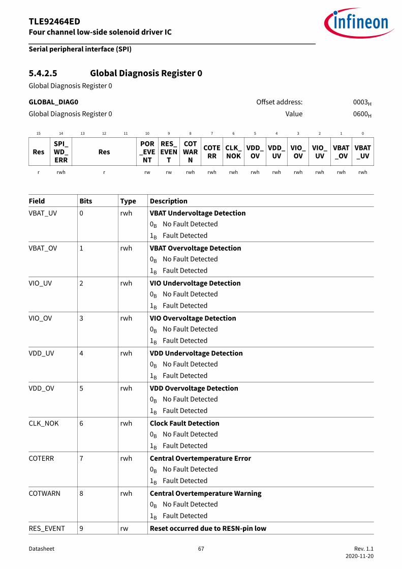
5.4.2.5 Global Diagnosis Register 0Global Diagnosis Register 0
GLOBAL_DIAG0 Offset address: 0003H
Global Diagnosis Register 0 Value 0600H
15 14 13 12 11 10 9 8 7 6 5 4 3 2 1 0
ResSPI_WD_ERR
ResPOR_EVE
NT
RES_EVEN
T
COTWAR
NCOTE
RRCLK_NOK
VDD_OV
VDD_UV
VIO_OV
VIO_UV
VBAT_OV
VBAT_UV
r rwh r rw rw rwh rwh rwh rwh rwh rwh rwh rwh rwh
Field Bits Type DescriptionVBAT_UV 0 rwh VBAT Undervoltage Detection
0B No Fault Detected1B Fault Detected
VBAT_OV 1 rwh VBAT Overvoltage Detection0B No Fault Detected1B Fault Detected
VIO_UV 2 rwh VIO Undervoltage Detection0B No Fault Detected1B Fault Detected
VIO_OV 3 rwh VIO Overvoltage Detection0B No Fault Detected1B Fault Detected
VDD_UV 4 rwh VDD Undervoltage Detection0B No Fault Detected1B Fault Detected
VDD_OV 5 rwh VDD Overvoltage Detection0B No Fault Detected1B Fault Detected
CLK_NOK 6 rwh Clock Fault Detection0B No Fault Detected1B Fault Detected
COTERR 7 rwh Central Overtemperature Error0B No Fault Detected1B Fault Detected
COTWARN 8 rwh Central Overtemperature Warning0B No Fault Detected1B Fault Detected
RES_EVENT 9 rw Reset occurred due to RESN-pin low
Serial peripheral interface (SPI)
Datasheet 67 Rev. 1.12020-11-20
TLE92464ED Four channel low-side solenoid driver IC
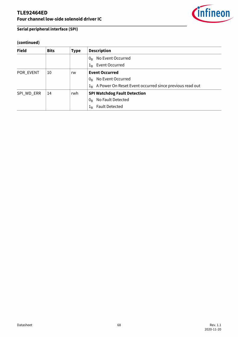
(continued)
Field Bits Type Description
0B No Event Occurred1B Event Occurred
POR_EVENT 10 rw Event Occurred0B No Event Occurred1B A Power On Reset Event occurred since previous read out
SPI_WD_ERR 14 rwh SPI Watchdog Fault Detection0B No Fault Detected1B Fault Detected
Serial peripheral interface (SPI)
Datasheet 68 Rev. 1.12020-11-20
TLE92464ED Four channel low-side solenoid driver IC
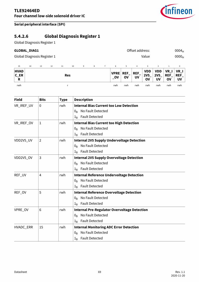
5.4.2.6 Global Diagnosis Register 1Global Diagnosis Register 1
GLOBAL_DIAG1 Offset address: 0004H
Global Diagnosis Register 1 Value 0000H
15 14 13 12 11 10 9 8 7 6 5 4 3 2 1 0
HVADC_ER
RRes VPRE
_OVREF_
OVREF_
UVVDD2V5_
OV
VDD2V5_
UV
VR_IREF_
OV
VR_IREF_
UVrwh r rwh rwh rwh rwh rwh rwh rwh
Field Bits Type DescriptionVR_IREF_UV 0 rwh Internal Bias Current too Low Detection
0B No Fault Detected1B Fault Detected
VR_IREF_OV 1 rwh Internal Bias Current too High Detection0B No Fault Detected1B Fault Detected
VDD2V5_UV 2 rwh Internal 2V5 Supply Undervoltage Detection0B No Fault Detected1B Fault Detected
VDD2V5_OV 3 rwh Internal 2V5 Supply Overvoltage Detection0B No Fault Detected1B Fault Detected
REF_UV 4 rwh Internal Reference Undervoltage Detection0B No Fault Detected1B Fault Detected
REF_OV 5 rwh Internal Reference Overvoltage Detection0B No Fault Detected1B Fault Detected
VPRE_OV 6 rwh Internal Pre-Regulator Overvoltage Detection0B No Fault Detected1B Fault Detected
HVADC_ERR 15 rwh Internal Monitoring ADC Error Detection0B No Fault Detected1B Fault Detected
Serial peripheral interface (SPI)
Datasheet 69 Rev. 1.12020-11-20
TLE92464ED Four channel low-side solenoid driver IC

5.4.2.7 Global Diagnosis Register 2Global Diagnosis Register 2
GLOBAL_DIAG2 Offset address: 0005H
Global Diagnosis Register 2 Value 0000H
15 14 13 12 11 10 9 8 7 6 5 4 3 2 1 0
ResOTP_VIRG
IN
OTP_ECC_ERR
OTP_ECC_WAR
N
REG_ECC_ERR
REG_ECC_WAR
Nr rwh rwh rwh rwh rwh
Field Bits Type DescriptionREG_ECC_WARN
0 rwh Register ECC Warning0B No Warning1B Single Bit Flip Detected and Corrected
REG_ECC_ERR 1 rwh Register ECC Error0B No Error1B Multi Bit Flip Detected
OTP_ECC_WARN
2 rwh OTP ECC Warning0B No Warning1B Repairable Bit Flip Detected
OTP_ECC_ERR 3 rwh OTP ECC Error0B No Error1B None Repairable Multi Bit Flip Detected
OTP_VIRGIN 4 rwh OTP Memory Configured Complete0B OTP completely configured1B Virgin OTP Address Detected
Serial peripheral interface (SPI)
Datasheet 70 Rev. 1.12020-11-20
TLE92464ED Four channel low-side solenoid driver IC
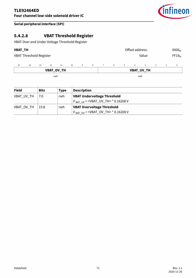
5.4.2.8 VBAT Threshold RegisterVBAT Over and Under Voltage Threshold Register
VBAT_TH Offset address: 0006H
VBAT Threshold Register Value FF19H
15 14 13 12 11 10 9 8 7 6 5 4 3 2 1 0
VBAT_OV_TH VBAT_UV_THrwh rwh
Field Bits Type DescriptionVBAT_UV_TH 7:0 rwh VBAT Undervoltage Threshold
V BAT_UV = <VBAT_UV_TH> * 0.16208 V
VBAT_OV_TH 15:8 rwh VBAT Overvoltage ThresholdV BAT_OV = <VBAT_OV_TH> * 0.16208 V
Serial peripheral interface (SPI)
Datasheet 71 Rev. 1.12020-11-20
TLE92464ED Four channel low-side solenoid driver IC
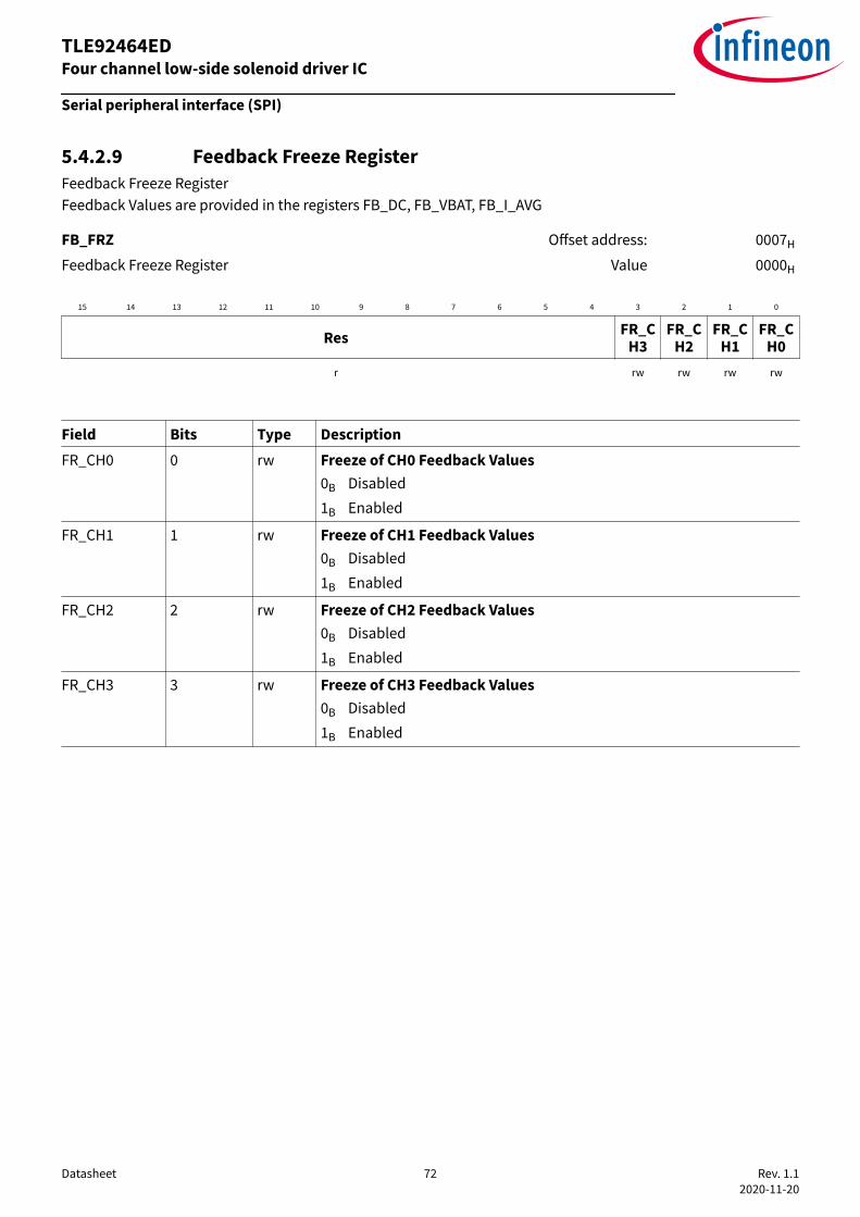
5.4.2.9 Feedback Freeze RegisterFeedback Freeze RegisterFeedback Values are provided in the registers FB_DC, FB_VBAT, FB_I_AVG
FB_FRZ Offset address: 0007H
Feedback Freeze Register Value 0000H
15 14 13 12 11 10 9 8 7 6 5 4 3 2 1 0
Res FR_CH3
FR_CH2
FR_CH1
FR_CH0
r rw rw rw rw
Field Bits Type DescriptionFR_CH0 0 rw Freeze of CH0 Feedback Values
0B Disabled1B Enabled
FR_CH1 1 rw Freeze of CH1 Feedback Values0B Disabled1B Enabled
FR_CH2 2 rw Freeze of CH2 Feedback Values0B Disabled1B Enabled
FR_CH3 3 rw Freeze of CH3 Feedback Values0B Disabled1B Enabled
Serial peripheral interface (SPI)
Datasheet 72 Rev. 1.12020-11-20
TLE92464ED Four channel low-side solenoid driver IC

5.4.2.10 Feedback Update RegisterFeedback Update RegisterFeedback Values are provided in the registers FB_DC, FB_VBAT, FB_I_AVG
FB_UPD Offset address: 0008H
Feedback Update Register Value 0000H
15 14 13 12 11 10 9 8 7 6 5 4 3 2 1 0
Res UD_CH3
UD_CH2
UD_CH1
UD_CH0
r rh rh rh rh
Field Bits Type DescriptionUD_CH0 0 rh Indication of CH0 Feedback Values Update
0B No new Feedback Values available1B New Feedback Values available
UD_CH1 1 rh Indication of CH1 Feedback Values Update0B No new Feedback Values available1B New Feedback Values available
UD_CH2 2 rh Indication of CH2 Feedback Values Update0B No new Feedback Values available1B New Feedback Values available
UD_CH3 3 rh Indication of CH3 Feedback Values Update0B No new Feedback Values available1B New Feedback Values available
Serial peripheral interface (SPI)
Datasheet 73 Rev. 1.12020-11-20
TLE92464ED Four channel low-side solenoid driver IC
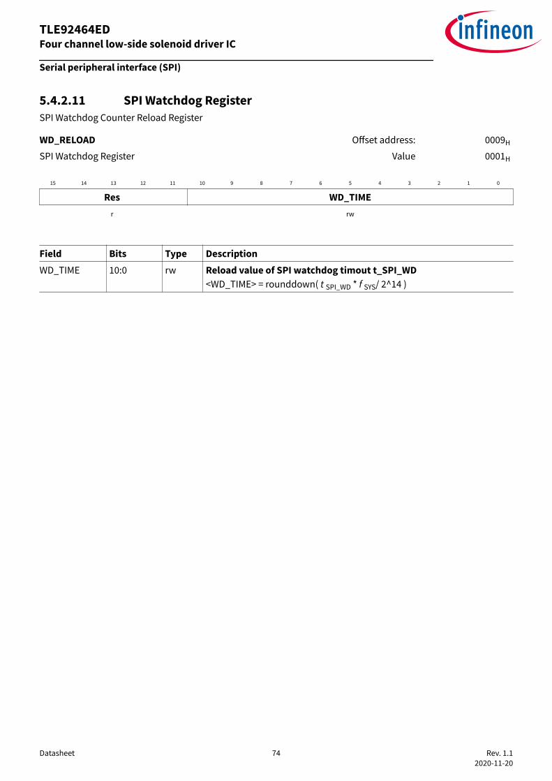
5.4.2.11 SPI Watchdog RegisterSPI Watchdog Counter Reload Register
WD_RELOAD Offset address: 0009H
SPI Watchdog Register Value 0001H
15 14 13 12 11 10 9 8 7 6 5 4 3 2 1 0
Res WD_TIMEr rw
Field Bits Type DescriptionWD_TIME 10:0 rw Reload value of SPI watchdog timout t_SPI_WD
<WD_TIME> = rounddown( t SPI_WD * f SYS/ 2^14 )
Serial peripheral interface (SPI)
Datasheet 74 Rev. 1.12020-11-20
TLE92464ED Four channel low-side solenoid driver IC

5.4.2.12 Diagnosis Error Register 0Diagnosis Error Register Channel Group 0
DIAG_ERR_CHGR0 Offset address: 000AH
Diagnosis Error Register 0 Value 0000H
15 14 13 12 11 10 9 8 7 6 5 4 3 2 1 0
Res OTE1 SG1 OC1 OL1 OLSG1 Res OTE0 SG0 OC0 OL0 OLS
G0r rwh rwh rwh rwh rwh r rwh rwh rwh rwh rwh
Field Bits Type DescriptionOLSG0 0 rwh Open Load or Short to Ground Detection CH0
0B No Fault Detected1B Fault Detected
OL0 1 rwh Open Load Detection CH00B No Fault Detected1B Fault Detected
OC0 2 rwh Overcurrent Detection CH00B No Fault Detected1B Fault Detected
SG0 3 rwh Short to Ground Detection CH00B No Fault Detected1B Fault Detected
OTE0 4 rwh Overtemperature Error Detection CH00B No Fault Detected1B Fault Detected
OLSG1 8 rwh Open Load or Short to Ground Detection CH10B No Fault Detected1B Fault Detected
OL1 9 rwh Open Load Detection CH10B No Fault Detected1B Fault Detected
OC1 10 rwh Overcurrent Detection CH10B No Fault Detected1B Fault Detected
SG1 11 rwh Short to Ground Detection CH10B No Fault Detected1B Fault Detected
OTE1 12 rwh Overtemperature Error Detection CH10B No Fault Detected
Serial peripheral interface (SPI)
Datasheet 75 Rev. 1.12020-11-20
TLE92464ED Four channel low-side solenoid driver IC

(continued)
Field Bits Type Description
1B Fault Detected
Serial peripheral interface (SPI)
Datasheet 76 Rev. 1.12020-11-20
TLE92464ED Four channel low-side solenoid driver IC

5.4.2.13 Diagnosis Error Register 1Diagnosis Error Register Channel Group 1
DIAG_ERR_CHGR1 Offset address: 000BH
Diagnosis Error Register 1 Value 0000H
15 14 13 12 11 10 9 8 7 6 5 4 3 2 1 0
Res OTE3 SG3 OC3 OL3 OLSG3 Res OTE2 SG2 OC2 OL2 OLS
G2r rwh rwh rwh rwh rwh r rwh rwh rwh rwh rwh
Field Bits Type DescriptionOLSG2 0 rwh Open Load or Short to Ground Detection CH2
0B No Fault Detected1B Fault Detected
OL2 1 rwh Open Load Detection CH20B No Fault Detected1B Fault Detected
OC2 2 rwh Overcurrent Detection CH20B No Fault Detected1B Fault Detected
SG2 3 rwh Short to Ground Detection CH20B No Fault Detected1B Fault Detected
OTE2 4 rwh Overtemperature Error Detection CH20B No Fault Detected1B Fault Detected
OLSG3 8 rwh Open Load or Short to Ground Detection CH30B No Fault Detected1B Fault Detected
OL3 9 rwh Open Load Detection CH30B No Fault Detected1B Fault Detected
OC3 10 rwh Overcurrent Detection CH30B No Fault Detected1B Fault Detected
SG3 11 rwh Short to Ground Detection CH30B No Fault Detected1B Fault Detected
OTE3 12 rwh Overtemperature Error Detection CH30B No Fault Detected
Serial peripheral interface (SPI)
Datasheet 77 Rev. 1.12020-11-20
TLE92464ED Four channel low-side solenoid driver IC

(continued)
Field Bits Type Description
1B Fault Detected
Serial peripheral interface (SPI)
Datasheet 78 Rev. 1.12020-11-20
TLE92464ED Four channel low-side solenoid driver IC

5.4.2.14 Diagnosis Warning Register 0Diagnosis Warning Register Channel Group 0
DIAG_WARN_CHGR0 Offset address: 0010H
Diagnosis Warning Register 0 Value 1010H
15 14 13 12 11 10 9 8 7 6 5 4 3 2 1 0
Res
OLSG_WARN
1_CHK_NOK
OLSG_WARN
1
OTW1
I_REG_WARN
1
PWM_REG_WARN1
Res
OLSG_WARN
0_CHK_NOK
OLSG_WARN
0
OTW0
I_REG_WARN
0
PWM_REG_WARN0
r rwh rwh rwh rwh rwh r rwh rwh rwh rwh rwh
Field Bits Type DescriptionPWM_REG_WARN0
0 rwh ICC PWM Regulation Warning Detection CH00B No Warning Detected1B Warning Detected
I_REG_WARN0 1 rwh ICC Current Regulation Warning CH00B No Warning Detected1B Warning Detected
OTW0 2 rwh Overtemperature Warning Detection CH00B No Warning Detected1B Warning Detected
OLSG_WARN0 3 rwh Open Load or Short to Ground Warning Detection CH00B No Warning Detected1B Warning Detected
OLSG_WARN0_CHK_NOK
4 rwh Open Load or Short to Ground Warning Detection performed CH00B OLSG Warning Detection performed1B OLSG Warning Detection not possible
PWM_REG_WARN1
8 rwh ICC PWM Regulation Warning Detection CH10B No Warning Detected1B Warning Detected
I_REG_WARN1 9 rwh ICC Current Regulation Warning CH10B No Warning Detected1B Warning Detected
OTW1 10 rwh Overtemperature Warning Detection CH10B No Warning Detected1B Warning Detected
OLSG_WARN1 11 rwh Open Load or Short to Ground Warning Detection CH10B No Warning Detected
Serial peripheral interface (SPI)
Datasheet 79 Rev. 1.12020-11-20
TLE92464ED Four channel low-side solenoid driver IC

(continued)
Field Bits Type Description
1B Warning Detected
OLSG_WARN1_CHK_NOK
12 rwh Open Load or Short to Ground Warning Detection performed CH10B OLSG Warning Detection performed1B OLSG Warning Detection not possible
Serial peripheral interface (SPI)
Datasheet 80 Rev. 1.12020-11-20
TLE92464ED Four channel low-side solenoid driver IC
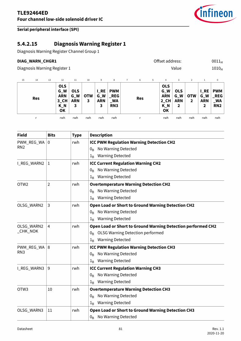
5.4.2.15 Diagnosis Warning Register 1Diagnosis Warning Register Channel Group 1
DIAG_WARN_CHGR1 Offset address: 0011H
Diagnosis Warning Register 1 Value 1010H
15 14 13 12 11 10 9 8 7 6 5 4 3 2 1 0
Res
OLSG_WARN
3_CHK_NOK
OLSG_WARN
3
OTW3
I_REG_WARN
3
PWM_REG_WARN3
Res
OLSG_WARN
2_CHK_NOK
OLSG_WARN
2
OTW2
I_REG_WARN
2
PWM_REG_WARN2
r rwh rwh rwh rwh rwh r rwh rwh rwh rwh rwh
Field Bits Type DescriptionPWM_REG_WARN2
0 rwh ICC PWM Regulation Warning Detection CH20B No Warning Detected1B Warning Detected
I_REG_WARN2 1 rwh ICC Current Regulation Warning CH20B No Warning Detected1B Warning Detected
OTW2 2 rwh Overtemperature Warning Detection CH20B No Warning Detected1B Warning Detected
OLSG_WARN2 3 rwh Open Load or Short to Ground Warning Detection CH20B No Warning Detected1B Warning Detected
OLSG_WARN2_CHK_NOK
4 rwh Open Load or Short to Ground Warning Detection performed CH20B OLSG Warning Detection performed1B Warning Detected
PWM_REG_WARN3
8 rwh ICC PWM Regulation Warning Detection CH30B No Warning Detected1B Warning Detected
I_REG_WARN3 9 rwh ICC Current Regulation Warning CH30B No Warning Detected1B Warning Detected
OTW3 10 rwh Overtemperature Warning Detection CH30B No Warning Detected1B Warning Detected
OLSG_WARN3 11 rwh Open Load or Short to Ground Warning Detection CH30B No Warning Detected
Serial peripheral interface (SPI)
Datasheet 81 Rev. 1.12020-11-20
TLE92464ED Four channel low-side solenoid driver IC

(continued)
Field Bits Type Description
1B Warning Detected
OLSG_WARN3_CHK_NOK
12 rwh Open Load or Short to Ground Warning Detection performed CH30B OLSG Warning Detection performed1B OLSG Warning Detection not possible
Serial peripheral interface (SPI)
Datasheet 82 Rev. 1.12020-11-20
TLE92464ED Four channel low-side solenoid driver IC

5.4.2.16 Fault Mask Register 0FAULTN-pin Mask 0 Register
FAULT_MASK0 Offset address: 0016H
Fault Mask Register 0 Value C00FH
15 14 13 12 11 10 9 8 7 6 5 4 3 2 1 0
SUP_NOK_EXT_MASK
SUP_NOK_INT_MASK
EN_PIN_MASK
ResCH3_ERR_MAS
K
CH2_ERR_MAS
K
CH1_ERR_MAS
K
CH0_ERR_MAS
K
rw rw rw r rw rw rw rw
Field Bits Type DescriptionCH0_ERR_MASK
0 rw OC0, SG0, OL0, OTE0, OLSG0 FAULTN-pin Indication0B Disabled1B Enabled
CH1_ERR_MASK
1 rw OC1, SG1, OL1, OTE1, OLSG1 FAULTN-pin Indication0B Disabled1B Enabled
CH2_ERR_MASK
2 rw OC2, SG2, OL2, OTE2, OLSG2 FAULTN-pin Indication0B Disabled1B Enabled
CH3_ERR_MASK
3 rw OC3, SG3, OL3, OTE3, OLSG3 FAULTN-pin Indication0B Disabled1B Enabled
EN_PIN_MASK 13 rw EN-pin Status at FAULTN-pin Indication0B Disabled1B Enabled
SUP_NOK_INT_MASK
14 rw Internal Supply UV/OV at FAULTN-pin Indication (SUP_NOK_INT)0B Disabled1B Enabled
SUP_NOK_EXT_MASK
15 rw External Supply UV/OV at FAULTN-pin Indication (SUP_NOK_EXT)0B Disabled1B Enabled
Serial peripheral interface (SPI)
Datasheet 83 Rev. 1.12020-11-20
TLE92464ED Four channel low-side solenoid driver IC

5.4.2.17 Fault Mask Register 1FAULTN-pin Mask 1 Register
FAULT_MASK1 Offset address: 0017H
Fault Mask Register 1 Value 700FH
15 14 13 12 11 10 9 8 7 6 5 4 3 2 1 0
ResCLK_LOW_MASK
COTERR_MAS
K
COTWARN_MASK
ResCH3_WARN_MASK
CH2_WARN_MASK
CH1_WARN_MASK
CH0_WARN_MASK
r rw rw rw r rw rw rw rw
Field Bits Type DescriptionCH0_WARN_MASK
0 rw CH0 Warning at FAULTN-pin Indication (OTW, I_REG_WARN,PWM_REG_WARN, OLSG_WARN)0B Disabled1B Enabled
CH1_WARN_MASK
1 rw CH1 Warning at FAULTN-pin Indication (OTW, I_REG_WARN,PWM_REG_WARN, OLSG_WARN)0B Disabled1B Enabled
CH2_WARN_MASK
2 rw CH2 Warning at FAULTN-pin Indication (OTW, I_REG_WARN,PWM_REG_WARN, OLSG_WARN)0B Disabled1B Enabled
CH3_WARN_MASK
3 rw CH3 Warning at FAULTN-pin Indication (OTW, I_REG_WARN,PWM_REG_WARN, OLSG_WARN)0B Disabled1B Enabled
COTWARN_MASK
12 rw Central Overtemperature Warning at FAULTN-pin Indication(COTWRN)0B Disabled1B Enabled
COTERR_MASK
13 rw Central Overtemperature Error at FAULTN-pin Indication (COTERR)0B Disabled1B Enabled
CLK_LOW_MASK
14 rw Clock too Slow at FAULTN-pin Indication (DIG_CLK_TOO_SLOW,CLK_TOO_SLOW)0B Disabled1B Enabled
Serial peripheral interface (SPI)
Datasheet 84 Rev. 1.12020-11-20
TLE92464ED Four channel low-side solenoid driver IC
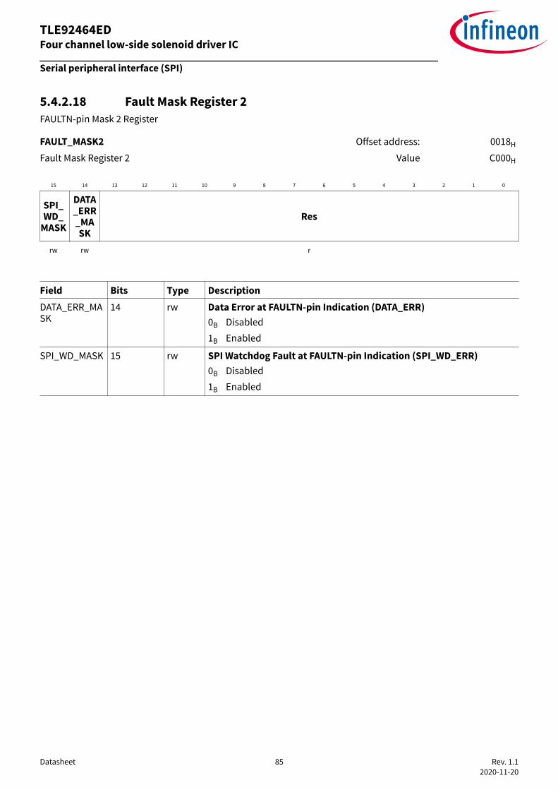
5.4.2.18 Fault Mask Register 2FAULTN-pin Mask 2 Register
FAULT_MASK2 Offset address: 0018H
Fault Mask Register 2 Value C000H
15 14 13 12 11 10 9 8 7 6 5 4 3 2 1 0
SPI_WD_
MASK
DATA_ERR_MASK
Res
rw rw r
Field Bits Type DescriptionDATA_ERR_MASK
14 rw Data Error at FAULTN-pin Indication (DATA_ERR)0B Disabled1B Enabled
SPI_WD_MASK 15 rw SPI Watchdog Fault at FAULTN-pin Indication (SPI_WD_ERR)0B Disabled1B Enabled
Serial peripheral interface (SPI)
Datasheet 85 Rev. 1.12020-11-20
TLE92464ED Four channel low-side solenoid driver IC

5.4.2.19 Clock Control RegisterClock Control Register: write access only possible in Config Mode
CLK_DIV Offset address: 0019H
Clock Control Register Value 0438H
15 14 13 12 11 10 9 8 7 6 5 4 3 2 1 0
EXT_CLK PLL_REFDIV PLL_FBDIV
rwh rw rw
Field Bits Type DescriptionPLL_FBDIV 8:0 rw PLL feedback divider
<PLL_FBDIV> = 56 MHz * <PLL_REFDIV> / f CLK
PLL_REFDIV 14:9 rw PLL reference divider<PLL_REFDIV> = round( f CLK / 1 MHz )
EXT_CLK 15 rwh Clock Source Selection0B Internal Clock1B External clock (CLK-pin)
Serial peripheral interface (SPI)
Datasheet 86 Rev. 1.12020-11-20
TLE92464ED Four channel low-side solenoid driver IC
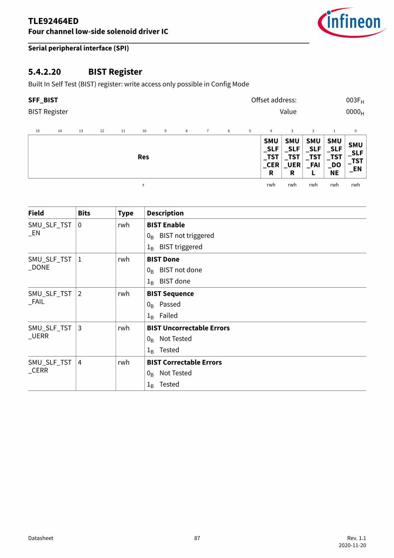
5.4.2.20 BIST RegisterBuilt In Self Test (BIST) register: write access only possible in Config Mode
SFF_BIST Offset address: 003FH
BIST Register Value 0000H
15 14 13 12 11 10 9 8 7 6 5 4 3 2 1 0
Res
SMU_SLF_TST_CER
R
SMU_SLF_TST_UER
R
SMU_SLF_TST_FAI
L
SMU_SLF_TST_DONE
SMU_SLF_TST_EN
r rwh rwh rwh rwh rwh
Field Bits Type DescriptionSMU_SLF_TST_EN
0 rwh BIST Enable0B BIST not triggered1B BIST triggered
SMU_SLF_TST_DONE
1 rwh BIST Done0B BIST not done1B BIST done
SMU_SLF_TST_FAIL
2 rwh BIST Sequence0B Passed1B Failed
SMU_SLF_TST_UERR
3 rwh BIST Uncorrectable Errors0B Not Tested1B Tested
SMU_SLF_TST_CERR
4 rwh BIST Correctable Errors0B Not Tested1B Tested
Serial peripheral interface (SPI)
Datasheet 87 Rev. 1.12020-11-20
TLE92464ED Four channel low-side solenoid driver IC

5.4.2.21 Version RegisterIC version and ID
ICVID Offset address: 0200H
Version Register Value C1XXH
15 14 13 12 11 10 9 8 7 6 5 4 3 2 1 0
MANUFACTURER VERSIONrh rh
Field Bits Type DescriptionVERSION 7:0 rh Chip Version
FCH B11 Design StepFDH B12 Design StepFEH B13 Design StepFFH B15 Design Step
MANUFACTURER
15:8 rh Manufacturer ID
Serial peripheral interface (SPI)
Datasheet 88 Rev. 1.12020-11-20
TLE92464ED Four channel low-side solenoid driver IC

5.4.2.22 Pin Status RegisterPin Status Feedback Register
PIN_STAT Offset address: 0201H
Pin Status Register Value 0000H
15 14 13 12 11 10 9 8 7 6 5 4 3 2 1 0
ResFAULTN_F
BFAUL
TN EN DRV3 DRV2 DRV1 DRV0
r rh rh rh rh rh rh rh
Field Bits Type DescriptionDRV0 0 rh Logic Level of DRV0-pin
0B Low1B High
DRV1 1 rh Logic Level of DRV1-pin0B Low1B High
DRV2 2 rh Logic Level of DRV2-pin0B Low1B High
DRV3 3 rh Logic Level of DRV3-pin0B Low1B High
EN 4 rh Logic Level of EN-pin0B Low1B High
FAULTN 5 rh Internal Status of FAULTN-pin according to Fault Mask Configuration0B Fault detected1B No Fault detected
FAULTN_FB 6 rh Logic Level of FAULTN-pin0B Low1B High
Serial peripheral interface (SPI)
Datasheet 89 Rev. 1.12020-11-20
TLE92464ED Four channel low-side solenoid driver IC

5.4.2.23 Feedback Status RegisterGeneral status register
FB_STAT Offset address: 0202H
Feedback Status Register Value 20 0618H
21 20 19 18 17 16
INIT_DON
E
SPI_WD_ERR
Res
rh rh r
15 14 13 12 11 10 9 8 7 6 5 4 3 2 1 0
ERR_CHGR
1
ERR_CHGR0
SUP_NOK_INT
SUP_NOK_EXT
DATA_err
POR_eve
nt
RES_even
t
COTWAR
NCOTE
RRCLK_NOK Res
OLSG_WARN_CHK_NOK_CHGR1
OLSG_WARN_CHK_NOK_CHGR0
Res
DIAG_WARN_CHGR1
DIAG_WARN_CHGR0
rh rh rh rh rh rh rh rh rh rh r rh rh r rh rh
Field Bits Type DescriptionDIAG_WARN_CHGR0
0 rh Current status of DIAG_WARN_CHGR0 register (excluding<OLSG_WARNx_CHK_NOK>)0B No Warning detected1B Warning detected
DIAG_WARN_CHGR1
1 rh Current status of DIAG_WARN_CHGR1 register (excluding<OLSG_WARNx_CHK_NOK>)0B No Warning detected1B Warning detected
OLSG_WARN_CHK_NOK_CHGR0
3 rh Current status of <OLSG_WARNx_CHK_NOK> bit in theDIAG_WARN_CHGR0 register0B No Warning detected1B Warning detected
OLSG_WARN_CHK_NOK_CHGR1
4 rh Current status of <OLSG_WARNx_CHK_NOK> bit in theDIAG_WARN_CHGR1 register0B No Warning detected1B Warning detected
CLK_NOK 6 rh Current status of CLK_NOK in GLOBAL_DIAG0 register0B No Fault detected1B Fault detected
COTERR 7 rh Current status of COTERR in GLOBAL DIAG0 register0B No Fault detected
Serial peripheral interface (SPI)
Datasheet 90 Rev. 1.12020-11-20
TLE92464ED Four channel low-side solenoid driver IC
(continued)
Field Bits Type Description
1B Fault detected
COTWARN 8 rh Current status of COTWARN in GLOBAL DIAG0 register0B No Warning detected1B Warning detected
RES_event 9 rh Current status of RES_event in GLOBAL DIAG0 register0B No Reset Event1B Reset occurred
POR_event 10 rh Current status of POR_event in GLOBAL DIAG0 register0B No power on Reset1B Power on Reset occurred
DATA_err 11 rh Current status of <OTP_ECC_ERR>, <OTP_VIRGIN>, <HV_ADC_ERR>0B No Fault detected1B Fault detected
SUP_NOK_EXT 12 rh Current status of <VIO_UV/OV>, <VDD_UV/OV>, <VBAT_UV/OV>0B No Fault detected1B Fault detected
SUP_NOK_INT 13 rh Current status of <VDD2V5_UV/OV>, <REF_UV/OV>, <VR_IREF_UV/OV>, <VPRE_OV>0B No Fault detected1B Fault detected
ERR_CHGR0 14 rh Current status of DIAG_ERR_CHGR1 register0B No Fault detected1B Fault detected
ERR_CHGR1 15 rh Current status of DIAG_ERR_CHGR2 register0B No Fault detected1B Fault detected
SPI_WD_ERR 20 rh Current status of <SPI_WD_ERR>0B No Fault detected1B Fault detected
INIT_DONE 21 rh Chip Initialization0B Not Done1B Done
Serial peripheral interface (SPI)
Datasheet 91 Rev. 1.12020-11-20
TLE92464ED Four channel low-side solenoid driver IC

5.4.2.24 Feedback Voltage Register 1Supply Voltage Feedback Register 1
FB_VOLTAGE1 Offset address: 0203H
Feedback Voltage Register 1 Value XX XXXXH
21 20 19 18 17 16
VDD rh
15 14 13 12 11 10 9 8 7 6 5 4 3 2 1 0
VDD VIOrh rh
Field Bits Type DescriptionVIO 10:0 rh VIO Voltage
V IO = 0.0034534 V * <VIO>
VDD 21:11 rh VDD VoltageV DD = 0.0034534 V * <VDD>
Serial peripheral interface (SPI)
Datasheet 92 Rev. 1.12020-11-20
TLE92464ED Four channel low-side solenoid driver IC

5.4.2.25 Feedback Voltage Register 2Supply Voltage Feedback Register 2
FB_VOLTAGE2 Offset address: 0204H
Feedback Voltage Register 2 Value XX XXXXH
21 20 19 18 17 16
VBAT rh
15 14 13 12 11 10 9 8 7 6 5 4 3 2 1 0
VBAT TEMP_VALUErh rh
Field Bits Type DescriptionTEMP_VALUE 10:0 rh Temperature Feedback
T FB =(<TEMP_VALUE>*0.000593 - 0.819 )/(-0.0016 ) [Celsius]
VBAT 21:11 rh VBAT VoltageV BAT = 41.47 V * <VBAT>/(2^11-1)
Serial peripheral interface (SPI)
Datasheet 93 Rev. 1.12020-11-20
TLE92464ED Four channel low-side solenoid driver IC

5.4.3 Channel registers
5.4.3.1 Register Overview - channelRegs (ascending Offset Address)
Table 21 Register Overview - channelRegs (ascending Offset Address)
Short Name Long Name OffsetAddress
PageNumber
SETPOINT Setpoint Register 0000H 95CTRL Control Register 0001H 96PERIOD ICC PWM Frequency Controller Register 0002H 97INTEGRATOR_LIMIT ICC Integrator Limitation Register 0003H 98DITHER_CLK_DIV Dither Clock Register 0004H 99DITHER_STEP Dither Step Register 0005H 100DITHER_CTRL Dither Control Register 0006H 101CH_CONFIG Channel Configuration Register 0007H 102MODE Channel Mode Register 000CH 104TON On-Time Register 000DH 105CTRL_INT_THRESH ICC Integrator Threshold Control Register 000EH 106FB_DC Feedback Duty Cycle Register 0200H 107FB_VBAT Feedback Average VBAT 0201H 108FB_I_AVG Feedback Average Current 0202H 109FB_IMIN_IMAX Feedback Min/Max Current 0203H 110FB_I_AVG_s16 Feedback signed Current 0204H 111FB_INT_THRESH Feedback ICC Integrator Threshold 0205H 112FB_PERIOD_MIN_MAX
Feedback Min/Max PWM Period 0206H 113
5.4.3.2 Register Address Space - channelRegs
Table 22 Registers Address Space - channelRegs
Module Base Address End Address Note
CH0 00000040H 0001003EH
CH1 00000050H 0001004EH
CH2 00000060H 0001005EH
CH3 00000070H 0001006EH
Serial peripheral interface (SPI)
Datasheet 94 Rev. 1.12020-11-20
TLE92464ED Four channel low-side solenoid driver IC
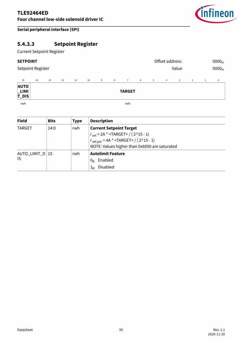
5.4.3.3 Setpoint RegisterCurrent Setpoint Register
SETPOINT Offset address: 0000H
Setpoint Register Value 0000H
15 14 13 12 11 10 9 8 7 6 5 4 3 2 1 0
AUTO_LIMIT_DIS
TARGET
rwh rwh
Field Bits Type DescriptionTARGET 14:0 rwh Current Setpoint Target
I set = 2A * <TARGET> / ( 2^15 - 1)I set,par = 4A * <TARGET> / ( 2^15 - 1)NOTE: Values higher than 0x6000 are saturated
AUTO_LIMIT_DIS
15 rwh Autolimit Feature0B Enabled1B Disabled
Serial peripheral interface (SPI)
Datasheet 95 Rev. 1.12020-11-20
TLE92464ED Four channel low-side solenoid driver IC

5.4.3.4 Control RegisterChannel Control Register
CTRL Offset address: 0001H
Control Register Value 4600H
15 14 13 12 11 10 9 8 7 6 5 4 3 2 1 0
ResOLSG_WARN_EN
OLSG_WARN_WINDOW
PWM_PERIOD_CALC_MODE
MIN_INT_THRESH
r rw rw rw rw
Field Bits Type DescriptionMIN_INT_THRESH
7:0 rw Minimum limit for ICC integrator thresholdThe value is signed: -128 to 127
PWM_PERIOD_CALC_MODE
8 rw ICC PWM controller does not consider falling Dither Slope0B No disabling of threshold calculation1B Skip threshold calculation on falling dither
OLSG_WARN_WINDOW
13:9 rw OLSG Warning Detection Blanking Timet OLwindow= (<OLSG_WARN_WINDOW>+1) * 64 * 1/ fsys
OLSG_WARN_EN
14 rw OLSG Warning Detection0B Disable warning1B Enable warning
Serial peripheral interface (SPI)
Datasheet 96 Rev. 1.12020-11-20
TLE92464ED Four channel low-side solenoid driver IC

5.4.3.5 ICC PWM Frequency Controller RegisterICC PWM Frequency Controller Register
PERIOD Offset address: 0002H
ICC PWM Frequency Controller Register Value 0000H
15 14 13 12 11 10 9 8 7 6 5 4 3 2 1 0
PWM_CTRL_PARAM
LOW_FREQ_RANGE_EN
PERIOD_EXP PERIOD_MANT
rw rw rw rw
Field Bits Type DescriptionPERIOD_MANT 7:0 rw Mantissa of PWM Target Frequency
t PWM = <PERIOD_MANT> * 2^<PERIOD_EXP> * 1/f sys<PERIOD_MANT> = 0 disables the ICC PWM Frequency Controller
PERIOD_EXP 10:8 rw Exponent of PWM Target Frequencyt PWM = <PERIOD_MANT> * 2^<PERIOD_EXP> * 1/f sys
LOW_FREQ_RANGE_EN
11 rw Low PWM Frequency Ranget PWM = <PERID_MANT> * 8 * 2^<PERIOD_EXP> * 1/f sys
0B Disabled1B Enabled
PWM_CTRL_PARAM
15:12 rw Control parameter ki of PWM Frequency Controller
Serial peripheral interface (SPI)
Datasheet 97 Rev. 1.12020-11-20
TLE92464ED Four channel low-side solenoid driver IC

5.4.3.6 ICC Integrator Limitation RegisterICC Integrator Limitation Register
INTEGRATOR_LIMIT Offset address: 0003H
ICC Integrator Limitation Register Value 43FFH
15 14 13 12 11 10 9 8 7 6 5 4 3 2 1 0
Res AUTO_LIM_VALUE_ABS LIM_VALUE_ABSr rw rw
Field Bits Type DescriptionLIM_VALUE_ABS
9:0 rw Absolut Integrator Limit of ICC
AUTO_LIM_VALUE_ABS
14:10 rw Integrator Limit of ICC after a setpoint update (Autolimit)
Serial peripheral interface (SPI)
Datasheet 98 Rev. 1.12020-11-20
TLE92464ED Four channel low-side solenoid driver IC
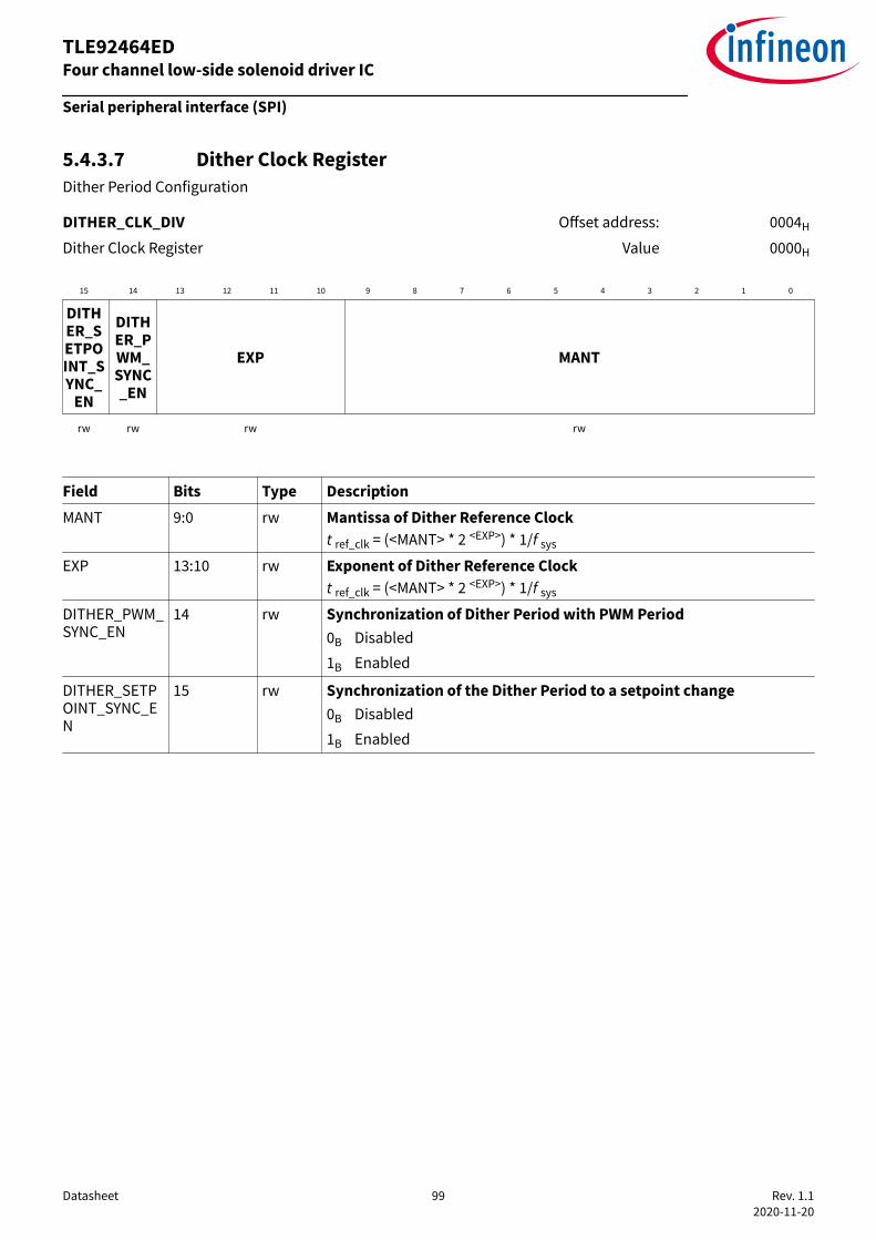
5.4.3.7 Dither Clock RegisterDither Period Configuration
DITHER_CLK_DIV Offset address: 0004H
Dither Clock Register Value 0000H
15 14 13 12 11 10 9 8 7 6 5 4 3 2 1 0
DITHER_SETPOINT_SYNC_
EN
DITHER_PWM_SYNC_EN
EXP MANT
rw rw rw rw
Field Bits Type DescriptionMANT 9:0 rw Mantissa of Dither Reference Clock
t ref_clk = (<MANT> * 2 <EXP>) * 1/f sys
EXP 13:10 rw Exponent of Dither Reference Clockt ref_clk = (<MANT> * 2 <EXP>) * 1/f sys
DITHER_PWM_SYNC_EN
14 rw Synchronization of Dither Period with PWM Period0B Disabled1B Enabled
DITHER_SETPOINT_SYNC_EN
15 rw Synchronization of the Dither Period to a setpoint change0B Disabled1B Enabled
Serial peripheral interface (SPI)
Datasheet 99 Rev. 1.12020-11-20
TLE92464ED Four channel low-side solenoid driver IC

5.4.3.8 Dither Step RegisterDither Amplitude Configuration
DITHER_STEP Offset address: 0005H
Dither Step Register Value 0000H
15 14 13 12 11 10 9 8 7 6 5 4 3 2 1 0
STEPS FLATrw rw
Field Bits Type DescriptionFLAT 7:0 rw Number of flat Dither Reference Clocks tref_clk on top and bottom
of the Dither waveformt flat= <FLAT> * t ref_clk
STEPS 15:8 rw Number of Dither steps within a quarter Dither PeriodT Dither = [4* (<STEPS>) + 2 * <FLAT> ] * t ref_clkI Dither =<STEPS>*<STEP_SIZE> * 2 A / (215-1)NOTE: If <STEP_SIZE> = 0, the dither overlay I Dither is disabled.NOTE: If <STEPS> = 0, the dither overlay I Dither is disabled and the ditherperiod T Dither is determined by <FLAT>NOTE: If <STEPS> = 0 and <FLAT> = 0, the dither period T Dither=t ref_clk
Serial peripheral interface (SPI)
Datasheet 100 Rev. 1.12020-11-20
TLE92464ED Four channel low-side solenoid driver IC

5.4.3.9 Dither Control RegisterDither Control Register
DITHER_CTRL Offset address: 0006H
Dither Control Register Value 0000H
15 14 13 12 11 10 9 8 7 6 5 4 3 2 1 0
ResDEEP_DITHE
RRes STEP_SIZE
r rw r rw
Field Bits Type DescriptionSTEP_SIZE 11:0 rw Size of Dither Steps resulting in a Dither Amplitude IDither
I Dither =<STEPS>*<STEP_SIZE> * 2 A / (215-1)
DEEP_DITHER 13 rw Deep Dither Feature0B Disabled1B Enabled
Serial peripheral interface (SPI)
Datasheet 101 Rev. 1.12020-11-20
TLE92464ED Four channel low-side solenoid driver IC

5.4.3.10 Channel Configuration RegisterChannel Configuration Register
CH_CONFIG Offset address: 0007H
Channel Configuration Register Value 0003H
15 14 13 12 11 10 9 8 7 6 5 4 3 2 1 0
OFF_DIAG_CH
OC_DIAG_EN
OL_TH_FIXED OL_TH I_DIAG SLEWR
rwh rwh rw rw rw rw
Field Bits Type DescriptionSLEWR 1:0 rw Channel Slew Rate
00B 1.0 V/us01B 2.5 V/us10B 5.0 V/us11B 10.0 V/us
I_DIAG 3:2 rw OFF-state Diagosis Current Strength00B 80 uA01B 190 uA10B 720 uA11B 1250 uA
OL_TH 6:4 rw Open Load Threshold relative to Setpoint000B Disabled001B 1/8 of Current Setpoint010B 2/8 of Current Setpoint011B 3/8 of Current Setpoint100B 4/8 of Current Setpoint101B 5/8 of Current Setpoint110B 6/8 of Current Setpoint111B 7/8 of Current Setpoint
OL_TH_FIXED 12:7 rw Fixed Open Load ThresholdI OLTH = <OL_TH_FIXED> * 128 * 2000mA / (2^15 - 1)I OLTH,parallel = <OL_TH_FIXED> * 128 * 4000mA / (2^15 - 1)
OC_DIAG_EN 13 rwh OC Diagnosis in OFF-state0B Disabled1B Enable Output Stage for t_OCon
tOCon = [(<TON_MANT>+1)*2^<EXP>)] * 1/fSYS
NOTE: <TON_MANT> is located in the TON register.NOTE: <EXP> is located in the DITHER_CLK_DIV register.
TLE92464ED Four channel low-side solenoid driver IC
Serial peripheral interface (SPI)
Datasheet 102 Rev. 1.12020-11-20

(continued)
Field Bits Type DescriptionOFF_DIAG_CH 15:14 rwh OFF-state Diagnosis Current Sources Control
00B OFF-state Diagnosis Enabled01B Low Side Current Source Enabled10B High Side Current Source Enabled11B OFF-state Diagnosis Disabled
Serial peripheral interface (SPI)
Datasheet 103 Rev. 1.12020-11-20
TLE92464ED Four channel low-side solenoid driver IC

5.4.3.11 Channel Mode RegisterChannel Mode Register: write access only possible in Config Mode
MODE Offset address: 000CH
Channel Mode Register Value 0000H
15 14 13 12 11 10 9 8 7 6 5 4 3 2 1 0
Res CH_MODEr rw
Field Bits Type DescriptionCH_MODE 3:0 rw Channel Operation Mode
0H Off1H ICC Current Control2H Direct Drive Mode via SPI on-time setting (TON
register)3H Direct Drive Mode via DRVx-pinCH Free running Measurement (2^16 samples)
Serial peripheral interface (SPI)
Datasheet 104 Rev. 1.12020-11-20
TLE92464ED Four channel low-side solenoid driver IC

5.4.3.12 On-Time RegisterDriver On-Time Configuration Register
TON Offset address: 000DH
On-Time Register Value 0000H
15 14 13 12 11 10 9 8 7 6 5 4 3 2 1 0
OLSG_TIMEOUT TON_MANTrw rw
Field Bits Type DescriptionTON_MANT 9:0 rw On-Time of Output stage (SPI Direct Drive Mode/OC-Detection)
t OCon = [(<TON_MANT>+1)*2^<EXP>)] * 1/f sysNOTE: For OC detection in OFF-state the maximum t on period is 300msand <TON_MANT> must be different to 0.t on = (<TON_MANT> * 2^<EXP>) * 1/f sysNOTE: The Period is derived from the Dither Period (DITHER_CLK_DIV)NOTE: <EXP> is located in the DITHER_CLK_DIV register
OLSG_TIMEOUT
15:10 rw Time out period for OLSG detectiont OLSG_TIMEOUT = (<OLSG_TIMEOUT> *256 +255) *64 * 1/f sys
Serial peripheral interface (SPI)
Datasheet 105 Rev. 1.12020-11-20
TLE92464ED Four channel low-side solenoid driver IC
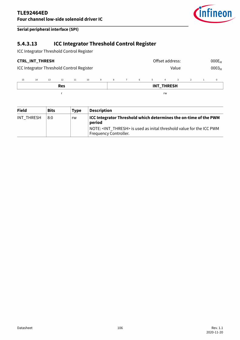
5.4.3.13 ICC Integrator Threshold Control RegisterICC Integrator Threshold Control Register
CTRL_INT_THRESH Offset address: 000EH
ICC Integrator Threshold Control Register Value 0003H
15 14 13 12 11 10 9 8 7 6 5 4 3 2 1 0
Res INT_THRESHr rw
Field Bits Type DescriptionINT_THRESH 8:0 rw ICC Integrator Threshold which determines the on-time of the PWM
periodNOTE: <INT_THRESH> is used as inital threshold value for the ICC PWMFrequency Controller.
Serial peripheral interface (SPI)
Datasheet 106 Rev. 1.12020-11-20
TLE92464ED Four channel low-side solenoid driver IC

5.4.3.14 Feedback Duty Cycle RegisterDuty Cycle Feedback ValueRead Only Register
FB_DC Offset address: 0200H
Feedback Duty Cycle Register Value 00 0000H
21 20 19 18 17 16
TO_MANT rh
15 14 13 12 11 10 9 8 7 6 5 4 3 2 1 0
TO_MANT TP_MANTrh rh
Field Bits Type DescriptionTP_MANT 10:0 rh Period Mantissa
T meas = <TP_MANT> * 2^<EXP> * 1/f sysNOTE: <EXP> is located in the FB_VBAT or FB_I_AVG register.
TO_MANT 21:11 rh On-time Mantissat ON = <TO_MANT>*2^<EXP> * 1/f sysDC = <TO_MANT>/<TP_MANT>NOTE: <EXP> is located in the FB_VBAT or FB_I_AVG register.
Serial peripheral interface (SPI)
Datasheet 107 Rev. 1.12020-11-20
TLE92464ED Four channel low-side solenoid driver IC

5.4.3.15 Feedback Average VBATAverage Battery Voltage (VBAT) Feedback RegisterRead Only Register
FB_VBAT Offset address: 0201H
Feedback Average VBAT Value 00 0000H
21 20 19 18 17 16
Res r
15 14 13 12 11 10 9 8 7 6 5 4 3 2 1 0
EXP Res VBAT_AVG_MANTrh r rh
Field Bits Type DescriptionVBAT_AVG_MANT
10:0 rh Average Battery Voltage MantissaV BAT = 41.47V * <VBAT_AVG_MANT>/<TP_MANT>NOTE: <TP_MANT> is located in the FB_DC register
EXP 15:12 rh Measurement Exponent
Serial peripheral interface (SPI)
Datasheet 108 Rev. 1.12020-11-20
TLE92464ED Four channel low-side solenoid driver IC

5.4.3.16 Feedback Average CurrentAverage Current Feedback ValueRead Only Register
FB_I_AVG Offset address: 0202H
Feedback Average Current Value 00 0000H
21 20 19 18 17 16
Res r
15 14 13 12 11 10 9 8 7 6 5 4 3 2 1 0
EXP I_AVG_MANTrh rh
Field Bits Type DescriptionI_AVG_MANT 11:0 rh Signed Mantissa of Average Current Feedback (two's complement)
I avg = 4A * <I_AVG_MANT> / <TP_MANT>NOTE: <TP_MANT> is located in the FB_DC register
EXP 15:12 rh Measurement Exponent
Serial peripheral interface (SPI)
Datasheet 109 Rev. 1.12020-11-20
TLE92464ED Four channel low-side solenoid driver IC

5.4.3.17 Feedback Min/Max CurrentMinimum/Maximum Current Feedback RegisterRead Only Register
FB_IMIN_IMAX Offset address: 0203H
Feedback Min/Max Current Value 00 0000H
21 20 19 18 17 16
Res IMAX r rh
15 14 13 12 11 10 9 8 7 6 5 4 3 2 1 0
IMAX IMINrh rh
Field Bits Type DescriptionIMIN 9:0 rh Signed Minimum Current of last measurement period (two's
complement)I min = <IMIN>*4A / (2^9-1)
IMAX 19:10 rh Signed Maximum Current of last measurement period (two'scomplement)I max = <IMAX>*4A / (2^9-1)
Serial peripheral interface (SPI)
Datasheet 110 Rev. 1.12020-11-20
TLE92464ED Four channel low-side solenoid driver IC
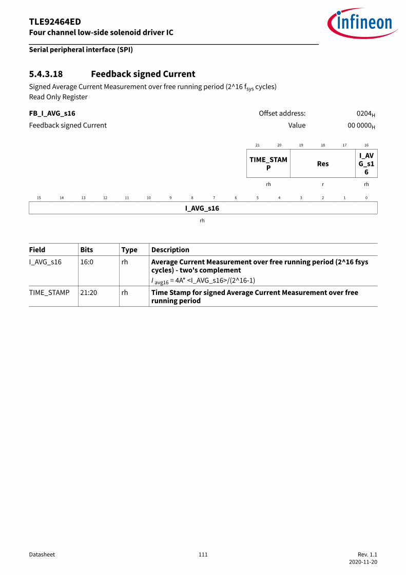
5.4.3.18 Feedback signed CurrentSigned Average Current Measurement over free running period (2^16 fsys cycles)Read Only Register
FB_I_AVG_s16 Offset address: 0204H
Feedback signed Current Value 00 0000H
21 20 19 18 17 16
TIME_STAMP Res
I_AVG_s1
6 rh r rh
15 14 13 12 11 10 9 8 7 6 5 4 3 2 1 0
I_AVG_s16rh
Field Bits Type DescriptionI_AVG_s16 16:0 rh Average Current Measurement over free running period (2^16 fsys
cycles) - two's complementI avg16 = 4A* <I_AVG_s16>/(2^16-1)
TIME_STAMP 21:20 rh Time Stamp for signed Average Current Measurement over freerunning period
Serial peripheral interface (SPI)
Datasheet 111 Rev. 1.12020-11-20
TLE92464ED Four channel low-side solenoid driver IC
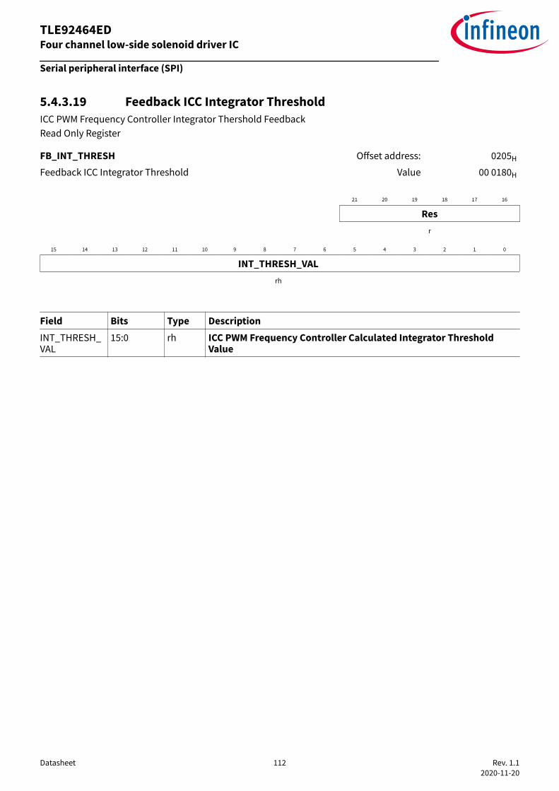
5.4.3.19 Feedback ICC Integrator ThresholdICC PWM Frequency Controller Integrator Thershold FeedbackRead Only Register
FB_INT_THRESH Offset address: 0205H
Feedback ICC Integrator Threshold Value 00 0180H
21 20 19 18 17 16
Res r
15 14 13 12 11 10 9 8 7 6 5 4 3 2 1 0
INT_THRESH_VALrh
Field Bits Type DescriptionINT_THRESH_VAL
15:0 rh ICC PWM Frequency Controller Calculated Integrator ThresholdValue
Serial peripheral interface (SPI)
Datasheet 112 Rev. 1.12020-11-20
TLE92464ED Four channel low-side solenoid driver IC

5.4.3.20 Feedback Min/Max PWM PeriodMinimum and Maximum PWM Frequency Feedback of last Measurement periodRead Only Register
FB_PERIOD_MIN_MAX Offset address: 0206H
Feedback Min/Max PWM Period Value 00 0000H
21 20 19 18 17 16
Res PMAX r rh
15 14 13 12 11 10 9 8 7 6 5 4 3 2 1 0
PMAX PMINrh rh
Field Bits Type DescriptionPMIN 9:0 rh Minimum PWM period of last Measurement period
f PWM_min = f sys / (<PMIN> * 256)
PMAX 19:10 rh Maximum PWM period of last Measurement periodf PWM_max = f sys / (<PMAX> * 256)
Serial peripheral interface (SPI)
Datasheet 113 Rev. 1.12020-11-20
TLE92464ED Four channel low-side solenoid driver IC

6 Application information The following application diagram shows how the IC is used in its environment.
Power Supply, Battery sense
andUnder/Over
Voltage Detection
PLL Clock Watchdog
Central Logic
CLK
VBAT
VDD
GND
RESN
SPIWatchdog
SPI
Channel Logic,Current Control,
Dither
CurrentSense
LoadDiagnostics
TemperatureSense
Low-sideGate Control
Overcurrent Protection
FWDx
LOADx
GNDPx
EN
SI
VIO
SCK
CSN
SO
DRVx
Low-side Solenoid Driver IC
FAULTN
Micro-Controller e.g. TC27x
Safety Switch Circuitry
Power-supply incl. High-side Driver e.g. TLE9243QK
VBAT
C4
C5
CLOADx
DxLx
GNDGND
... Channel x
GN
D
RSTP
N
WD
ON
V5C
U
VIO
SSxG
Reverse polarity Protection
andFilter
GND
GND
Vsup
GND
SSxS
SSxD
SSxSense
GN
D
GND
C3
R
C2
C1
CFWDx
CLOADy
R = 10kΩ C1 = 100µFC2 = C3 = C4 = C5 = 100nFCLOADx= 4.7nF…10nFrecommended: CLOADy = 4.7nF…10nF; CLOADx= CLOADy/10; CFWDx = 4.7nF…10nF
Note: This is a simplified example of an application circuit with focus on the Low-side Solenoid Driver IC. The function must be verified in the real application.
Figure 26 Simplified Application Circuit
Application information
Datasheet 114 Rev. 1.12020-11-20
TLE92464ED Four channel low-side solenoid driver IC

7 Package dimensions
Figure 27 Package outlines
Green ProductTo meet the world-wide customer requirements for environmentally friendly products and to be compliant withthe government regulations the device is available as a Green Product. Green Products are RoHS compliant(Pb-free finish on leads and suitable for Pb-free soldering according to IPC/JEDEC J-STD-020).
Package dimensions
Datasheet 115 Rev. 1.12020-11-20
TLE92464ED Four channel low-side solenoid driver IC

Revision historyRevision Date Changes
Datasheet v1.1 2020-11-20 • Equation for TDither added in "Dither configuration" chapter• Equation in chapter "Average feedback values" Tperiode renamed to
Tmeas
• Equation for ROL: "*" replaced by "-"• Pin list: cooling tap comment updated to "Connect externally to GND
and heat sink area" non-content updates (e.g. typo correction/wording refinement) in section:• Voltage Monitoring• Operation States• PWM frequency control• Dither parameter update• Dither setpoint synchronization• Direct Drive• OL-Threshold configuration• Overcurrent
Datasheet v1.0 2020-07-17 initial release
Revision history
Datasheet 116 Rev. 1.12020-11-20
TLE92464ED Four channel low-side solenoid driver IC

TrademarksAll referenced product or service names and trademarks are the property of their respective owners.
Edition 2020-11-20 Published by Infineon Technologies AG 81726 Munich, Germany © 2020 Infineon Technologies AG All Rights Reserved. Do you have a question about any aspect of this document? Email: [email protected] Document reference IFX-Z8F57255371
IMPORTANT NOTICEThe information given in this document shall in noevent be regarded as a guarantee of conditions orcharacteristics (“Beschaffenheitsgarantie”).With respect to any examples, hints or any typicalvalues stated herein and/or any information regardingthe application of the product, Infineon Technologieshereby disclaims any and all warranties and liabilitiesof any kind, including without limitation warranties ofnon-infringement of intellectual property rights of anythird party.In addition, any information given in this document issubject to customer’s compliance with its obligationsstated in this document and any applicable legalrequirements, norms and standards concerningcustomer’s products and any use of the product ofInfineon Technologies in customer’s applications.The data contained in this document is exclusivelyintended for technically trained staff. It is theresponsibility of customer’s technical departments toevaluate the suitability of the product for the intendedapplication and the completeness of the productinformation given in this document with respect to suchapplication.
WARNINGSDue to technical requirements products may containdangerous substances. For information on the typesin question please contact your nearest InfineonTechnologies office.Except as otherwise explicitly approved by InfineonTechnologies in a written document signed byauthorized representatives of Infineon Technologies,Infineon Technologies’ products may not be used inany applications where a failure of the product orany consequences of the use thereof can reasonablybe expected to result in personal injury.


