
TMS320C55x DSPCPU
Reference Guide
Literature Number: SPRU371FFebruary 2004

IMPORTANT NOTICE
Texas Instruments Incorporated and its subsidiaries (TI) reserve the right to make corrections,modifications, enhancements, improvements, and other changes to its products and services at anytime and to discontinue any product or service without notice. Customers should obtain the latestrelevant information before placing orders and should verify that such information is current andcomplete. All products are sold subject to TI’s terms and conditions of sale supplied at the time of orderacknowledgment.
TI warrants performance of its hardware products to the specifications applicable at the time of salein accordance with TI’s standard warranty. Testing and other quality control techniques are used to theextent TI deems necessary to support this warranty. Except where mandated by governmentrequirements, testing of all parameters of each product is not necessarily performed.
TI assumes no liability for applications assistance or customer product design. Customers areresponsible for their products and applications using TI components. To minimize the risks associatedwith customer products and applications, customers should provide adequate design and operatingsafeguards.
TI does not warrant or represent that any license, either express or implied, is granted under any TIpatent right, copyright, mask work right, or other TI intellectual property right relating to anycombination, machine, or process in which TI products or services are used. Information published byTI regarding third-party products or services does not constitute a license from TI to use such productsor services or a warranty or endorsement thereof. Use of such information may require a license froma third party under the patents or other intellectual property of the third party, or a license from TI underthe patents or other intellectual property of TI.
Reproduction of information in TI data books or data sheets is permissible only if reproduction is withoutalteration and is accompanied by all associated warranties, conditions, limitations, and notices.Reproduction of this information with alteration is an unfair and deceptive business practice. TI is notresponsible or liable for such altered documentation.
Resale of TI products or services with statements different from or beyond the parameters stated byTI for that product or service voids all express and any implied warranties for the associated TI productor service and is an unfair and deceptive business practice. TI is not responsible or liable for any suchstatements.
Following are URLs where you can obtain information on other Texas Instruments products andapplication solutions:
Products Applications
Amplifiers amplifier.ti.com Audio www.ti.com/audio
Data Converters dataconverter.ti.com Automotive www.ti.com/automotive
DSP dsp.ti.com Broadband www.ti.com/broadband
Interface interface.ti.com Digital Control www.ti.com/digitalcontrol
Logic logic.ti.com Military www.ti.com/military
Power Mgmt power.ti.com Optical Networking www.ti.com/opticalnetwork
Microcontrollers microcontroller.ti.com Security www.ti.com/security
Telephony www.ti.com/telephony
Video & Imaging www.ti.com/video
Wireless www.ti.com/wireless
Mailing Address: Texas Instruments
Post Office Box 655303 Dallas, Texas 75265
Copyright 2004, Texas Instruments Incorporated

iiiRead This First
Preface
Read This First
About This Manual
This manual describes the central processing unit (CPU) of theTMS320C55x (C55x) fixed-point digital signal processors (DSPs): thearchitecture, registers, and operation.
Notational Conventions
This document uses the following conventions.
� If a signal or pin is active low, it has an overbar. For example, the RESETsignal is active low.
� In most cases, hexadecimal numbers are shown with the suffix h. Forexample, the following number is a hexadecimal 40 (decimal 64):
40h
Similarly, binary numbers usually are shown with the suffix b. For example,the following number is the decimal number 4 shown in binary form:
0100b
� Bits and signals are sometimes referenced with the following notations:
Notation Description Example
Register(n−m) Bits n through m of Register AC0(15−0) represents bits 15through 0 of the register AC0.
Bus[n:m] Signals n through m of Bus A[21:1] represents signals 21through 1 of bus A.

Related Documentation From Texas Instruments
iv
� The following terms are used to name portions of data:
Term Description Example
LSB Least significant bit In AC0(15−0), bit 0 is the LSB.
MSB Most significant bit In AC0(15−0), bit 15 is the MSB.
LSByte Least significant byte In AC0(15−0), bits 7−0 are the LSByte.
MSByte Most significant byte In AC0(15−0), bits 15−8 are the MSByte.
LSW Least significant word In AC0(31−0), bits 15−0 are the LSW.
MSW Most significant word In AC0(31−0), bits 31−16 are the MSW.
Related Documentation From Texas Instruments
The following documents describe the C55x devices and related support tools.Copies of these documents are available on the Internet at www.ti.com.Tip: Enter the literature number in the search box provided at www.ti.com.
TMS320C55x Technical Overview (literature number SPRU393) introducesthe TMS320C55x DSPs, the latest generation of fixed-point DSPs in theTMS320C5000 DSP platform. Like the previous generations, thisprocessor is optimized for high performance and low-power operation.This book describes the CPU architecture, low-power enhancements,and embedded emulation features.
TMS320C55x DSP Peripherals Overview Reference Guide (literaturenumber SPRU317) introduces the peripherals, interfaces, and relatedhardware that are available on TMS320C55x DSPs.
TMS320C55x DSP Algebraic Instruction Set Reference Guide (literaturenumber SPRU375) describes the TMS320C55x DSP algebraicinstructions individually. Also includes a summary of the instruction set,a list of the instruction opcodes, and a cross-reference to the mnemonicinstruction set.
TMS320C55x DSP Mnemonic Instruction Set Reference Guide (literaturenumber SPRU374) describes the TMS320C55x DSP mnemonicinstructions individually. Also includes a summary of the instruction set,a list of the instruction opcodes, and a cross-reference to the algebraicinstruction set.
TMS320C55x Optimizing C/C++ Compiler User’s Guide (literature numberSPRU281) describes the TMS320C55x C/C++ Compiler. This C/C++compiler accepts ISO standard C and C++ source code and producesassembly language source code for TMS320C55x devices.
Notational Conventions / Related Documentation From Texas Instruments

Trademarks
vRead This First
TMS320C55x Assembly Language Tools User’s Guide (literature numberSPRU280) describes the assembly language tools (assembler, linker,and other tools used to develop assembly language code), assemblerdirectives, macros, common object file format, and symbolic debuggingdirectives for TMS320C55x devices.
TMS320C55x DSP Programmer’s Guide (literature number SPRU376)describes ways to optimize C and assembly code for the TMS320C55xDSPs and explains how to write code that uses special features andinstructions of the DSPs.
Trademarks
TMS320C5000, TMS320C54x, C54x, TMS320C55x, and C55x aretrademarks of Texas Instruments.
Related Documentation From Texas Instruments / Trademarks

vi
This page is intentionally left blank.

Contents
vii
Contents
1 CPU Architecture 1-1. . . . . . . . . . . . . . . . . . . . . . . . . . . . . . . . . . . . . . . . . . . . . . . . . . . . . . . . . . . . . . . 1.1 Overview of the CPU Architecture 1-2. . . . . . . . . . . . . . . . . . . . . . . . . . . . . . . . . . . . . . . . . . . .
1.1.1 Internal Data and Address Buses 1-3. . . . . . . . . . . . . . . . . . . . . . . . . . . . . . . . . . . . . 1.1.2 Memory Interface Unit 1-4. . . . . . . . . . . . . . . . . . . . . . . . . . . . . . . . . . . . . . . . . . . . . . . 1.1.3 Instruction Buffer Unit (I Unit) 1-4. . . . . . . . . . . . . . . . . . . . . . . . . . . . . . . . . . . . . . . . . 1.1.4 Program Flow Unit (P Unit) 1-4. . . . . . . . . . . . . . . . . . . . . . . . . . . . . . . . . . . . . . . . . . . 1.1.5 Address-Data Flow Unit (A Unit) 1-5. . . . . . . . . . . . . . . . . . . . . . . . . . . . . . . . . . . . . . 1.1.6 Data Computation Unit (D Unit) 1-5. . . . . . . . . . . . . . . . . . . . . . . . . . . . . . . . . . . . . . .
1.2 Instruction Buffer Unit (I Unit) 1-6. . . . . . . . . . . . . . . . . . . . . . . . . . . . . . . . . . . . . . . . . . . . . . . . 1.2.1 Instruction Buffer Queue 1-6. . . . . . . . . . . . . . . . . . . . . . . . . . . . . . . . . . . . . . . . . . . . . 1.2.2 Instruction Decoder 1-7. . . . . . . . . . . . . . . . . . . . . . . . . . . . . . . . . . . . . . . . . . . . . . . . .
1.3 Program Flow Unit (P Unit) 1-9. . . . . . . . . . . . . . . . . . . . . . . . . . . . . . . . . . . . . . . . . . . . . . . . . . 1.3.1 Program-Address Generation and Program-Control Logic 1-9. . . . . . . . . . . . . . . . 1.3.2 P-Unit Registers 1-10. . . . . . . . . . . . . . . . . . . . . . . . . . . . . . . . . . . . . . . . . . . . . . . . . . .
1.4 Address-Data Flow Unit (A Unit) 1-12. . . . . . . . . . . . . . . . . . . . . . . . . . . . . . . . . . . . . . . . . . . . 1.4.1 Data-Address Generation Unit (DAGEN) 1-13. . . . . . . . . . . . . . . . . . . . . . . . . . . . . . 1.4.2 A-Unit Arithmetic Logic Unit (A-Unit ALU) 1-13. . . . . . . . . . . . . . . . . . . . . . . . . . . . . . 1.4.3 A-Unit Registers 1-13. . . . . . . . . . . . . . . . . . . . . . . . . . . . . . . . . . . . . . . . . . . . . . . . . . .
1.5 Data Computation Unit (D Unit) 1-14. . . . . . . . . . . . . . . . . . . . . . . . . . . . . . . . . . . . . . . . . . . . . 1.5.1 Shifter 1-15. . . . . . . . . . . . . . . . . . . . . . . . . . . . . . . . . . . . . . . . . . . . . . . . . . . . . . . . . . . . 1.5.2 D-Unit Arithmetic Logic Unit (D-Unit ALU) 1-16. . . . . . . . . . . . . . . . . . . . . . . . . . . . . 1.5.3 Two Multiply-and-Accumulate Units (MACs) 1-16. . . . . . . . . . . . . . . . . . . . . . . . . . . 1.5.4 D-Unit Registers 1-16. . . . . . . . . . . . . . . . . . . . . . . . . . . . . . . . . . . . . . . . . . . . . . . . . . .
1.6 Address Buses and Data Buses 1-17. . . . . . . . . . . . . . . . . . . . . . . . . . . . . . . . . . . . . . . . . . . . . 1.7 Instruction Pipeline 1-20. . . . . . . . . . . . . . . . . . . . . . . . . . . . . . . . . . . . . . . . . . . . . . . . . . . . . . . .
1.7.1 Pipeline Phases 1-20. . . . . . . . . . . . . . . . . . . . . . . . . . . . . . . . . . . . . . . . . . . . . . . . . . . 1.7.2 Pipeline Protection 1-23. . . . . . . . . . . . . . . . . . . . . . . . . . . . . . . . . . . . . . . . . . . . . . . . .
2 CPU Registers 2-1. . . . . . . . . . . . . . . . . . . . . . . . . . . . . . . . . . . . . . . . . . . . . . . . . . . . . . . . . . . . . . . . . . 2.1 Alphabetical Summary of Registers 2-2. . . . . . . . . . . . . . . . . . . . . . . . . . . . . . . . . . . . . . . . . . . 2.2 Memory-Mapped Registers 2-4. . . . . . . . . . . . . . . . . . . . . . . . . . . . . . . . . . . . . . . . . . . . . . . . . . 2.3 Accumulators (AC0−AC3) 2-9. . . . . . . . . . . . . . . . . . . . . . . . . . . . . . . . . . . . . . . . . . . . . . . . . . . 2.4 Transition Registers (TRN0, TRN1) 2-10. . . . . . . . . . . . . . . . . . . . . . . . . . . . . . . . . . . . . . . . . . 2.5 Temporary Registers (T0−T3) 2-11. . . . . . . . . . . . . . . . . . . . . . . . . . . . . . . . . . . . . . . . . . . . . . .

Contents
viii
2.6 Registers Used to Address Data Space and I/O Space 2-12. . . . . . . . . . . . . . . . . . . . . . . . . 2.6.1 Auxiliary Registers (XAR0–XAR7 / AR0–AR7) 2-12. . . . . . . . . . . . . . . . . . . . . . . . . 2.6.2 Coefficient Data Pointer (XCDP / CDP) 2-14. . . . . . . . . . . . . . . . . . . . . . . . . . . . . . . 2.6.3 Circular Buffer Start Address Registers (BSA01, BSA23, BSA45,
BSA67, BSAC) 2-15. . . . . . . . . . . . . . . . . . . . . . . . . . . . . . . . . . . . . . . . . . . . . . . . . . . . 2.6.4 Circular Buffer Size Registers (BK03, BK47, BKC) 2-16. . . . . . . . . . . . . . . . . . . . . . 2.6.5 Data Page Register (XDP / DP) 2-17. . . . . . . . . . . . . . . . . . . . . . . . . . . . . . . . . . . . . . 2.6.6 Peripheral Data Page Register (PDP) 2-18. . . . . . . . . . . . . . . . . . . . . . . . . . . . . . . . . 2.6.7 Stack Pointers (XSP / SP, XSSP / SSP) 2-18. . . . . . . . . . . . . . . . . . . . . . . . . . . . . . .
2.7 Program Flow Registers (PC, RETA, CFCT) 2-21. . . . . . . . . . . . . . . . . . . . . . . . . . . . . . . . . . 2.7.1 Context Bits Stored in CFCT 2-21. . . . . . . . . . . . . . . . . . . . . . . . . . . . . . . . . . . . . . . . .
2.8 Registers for Managing Interrupts 2-23. . . . . . . . . . . . . . . . . . . . . . . . . . . . . . . . . . . . . . . . . . . 2.8.1 Interrupt Vector Pointers (IVPD, IVPH) 2-23. . . . . . . . . . . . . . . . . . . . . . . . . . . . . . . . 2.8.2 Interrupt Flag Registers (IFR0, IFR1) 2-24. . . . . . . . . . . . . . . . . . . . . . . . . . . . . . . . . 2.8.3 Interrupt Enable Registers (IER0, IER1) 2-27. . . . . . . . . . . . . . . . . . . . . . . . . . . . . . . 2.8.4 Debug Interrupt Enable Registers (DBIER0, DBIER1) 2-30. . . . . . . . . . . . . . . . . . .
2.9 Registers for Controlling Repeat Loops 2-34. . . . . . . . . . . . . . . . . . . . . . . . . . . . . . . . . . . . . . . 2.9.1 Single-Repeat Registers (RPTC, CSR) 2-34. . . . . . . . . . . . . . . . . . . . . . . . . . . . . . . . 2.9.2 Block-Repeat Registers (BRC0, BRC1, BRS1, RSA0, RSA1,
REA0, REA1) 2-34. . . . . . . . . . . . . . . . . . . . . . . . . . . . . . . . . . . . . . . . . . . . . . . . . . . . . 2.10 Status Registers (ST0_55−ST3_55) 2-37. . . . . . . . . . . . . . . . . . . . . . . . . . . . . . . . . . . . . . . . .
2.10.1 ST0_55 Bits 2-39. . . . . . . . . . . . . . . . . . . . . . . . . . . . . . . . . . . . . . . . . . . . . . . . . . . . . . . 2.10.2 ST1_55 Bits 2-42. . . . . . . . . . . . . . . . . . . . . . . . . . . . . . . . . . . . . . . . . . . . . . . . . . . . . . . 2.10.3 ST2_55 Bits 2-52. . . . . . . . . . . . . . . . . . . . . . . . . . . . . . . . . . . . . . . . . . . . . . . . . . . . . . . 2.10.4 ST3_55 Bits 2-56. . . . . . . . . . . . . . . . . . . . . . . . . . . . . . . . . . . . . . . . . . . . . . . . . . . . . . .
3 Memory and I/O Space 3-1. . . . . . . . . . . . . . . . . . . . . . . . . . . . . . . . . . . . . . . . . . . . . . . . . . . . . . . . . . 3.1 Memory Map 3-2. . . . . . . . . . . . . . . . . . . . . . . . . . . . . . . . . . . . . . . . . . . . . . . . . . . . . . . . . . . . . . 3.2 Program Space 3-3. . . . . . . . . . . . . . . . . . . . . . . . . . . . . . . . . . . . . . . . . . . . . . . . . . . . . . . . . . . .
3.2.1 Byte Addresses (24 Bits) 3-3. . . . . . . . . . . . . . . . . . . . . . . . . . . . . . . . . . . . . . . . . . . . . 3.2.2 Instruction Organization in Program Space 3-3. . . . . . . . . . . . . . . . . . . . . . . . . . . . . 3.2.3 Alignment of Fetches From Program Space 3-4. . . . . . . . . . . . . . . . . . . . . . . . . . . .
3.3 Data Space 3-5. . . . . . . . . . . . . . . . . . . . . . . . . . . . . . . . . . . . . . . . . . . . . . . . . . . . . . . . . . . . . . . 3.3.1 Word Addresses (23 Bits) 3-5. . . . . . . . . . . . . . . . . . . . . . . . . . . . . . . . . . . . . . . . . . . . 3.3.2 Data Types 3-5. . . . . . . . . . . . . . . . . . . . . . . . . . . . . . . . . . . . . . . . . . . . . . . . . . . . . . . . 3.3.3 Data Organization in Data Space 3-7. . . . . . . . . . . . . . . . . . . . . . . . . . . . . . . . . . . . . .
3.4 I/O Space 3-8. . . . . . . . . . . . . . . . . . . . . . . . . . . . . . . . . . . . . . . . . . . . . . . . . . . . . . . . . . . . . . . . . 3.5 Boot Loader 3-8. . . . . . . . . . . . . . . . . . . . . . . . . . . . . . . . . . . . . . . . . . . . . . . . . . . . . . . . . . . . . . .
4 Stack Operation 4-1. . . . . . . . . . . . . . . . . . . . . . . . . . . . . . . . . . . . . . . . . . . . . . . . . . . . . . . . . . . . . . . . 4.1 Data Stack and System Stack 4-2. . . . . . . . . . . . . . . . . . . . . . . . . . . . . . . . . . . . . . . . . . . . . . . 4.2 Stack Configurations 4-4. . . . . . . . . . . . . . . . . . . . . . . . . . . . . . . . . . . . . . . . . . . . . . . . . . . . . . . 4.3 Fast Return Versus Slow Return 4-5. . . . . . . . . . . . . . . . . . . . . . . . . . . . . . . . . . . . . . . . . . . . . 4.4 Automatic Context Switching 4-8. . . . . . . . . . . . . . . . . . . . . . . . . . . . . . . . . . . . . . . . . . . . . . . .
4.4.1 Fast-Return Context Switching for Calls 4-8. . . . . . . . . . . . . . . . . . . . . . . . . . . . . . . . 4.4.2 Fast-Return Context Switching for Interrupts 4-9. . . . . . . . . . . . . . . . . . . . . . . . . . . . 4.4.3 Slow-Return Context Switching for Calls 4-10. . . . . . . . . . . . . . . . . . . . . . . . . . . . . . 4.4.4 Slow-Return Context Switching for Interrupts 4-10. . . . . . . . . . . . . . . . . . . . . . . . . .

Contents
ixContents
5 Interrupts and Reset Operations 5-1. . . . . . . . . . . . . . . . . . . . . . . . . . . . . . . . . . . . . . . . . . . . . . . . . 5.1 Introduction to the Interrupts 5-2. . . . . . . . . . . . . . . . . . . . . . . . . . . . . . . . . . . . . . . . . . . . . . . . . 5.2 Interrupt Vectors and Priorities 5-4. . . . . . . . . . . . . . . . . . . . . . . . . . . . . . . . . . . . . . . . . . . . . . . 5.3 Maskable Interrupts 5-8. . . . . . . . . . . . . . . . . . . . . . . . . . . . . . . . . . . . . . . . . . . . . . . . . . . . . . . .
5.3.1 Bit and Registers Used to Enable Maskable Interrupts 5-9. . . . . . . . . . . . . . . . . . . 5.3.2 Standard Process Flow for Maskable Interrupts 5-9. . . . . . . . . . . . . . . . . . . . . . . . . 5.3.3 Process Flow for Time-Critical Interrupts 5-12. . . . . . . . . . . . . . . . . . . . . . . . . . . . . .
5.4 Nonmaskable Interrupts 5-14. . . . . . . . . . . . . . . . . . . . . . . . . . . . . . . . . . . . . . . . . . . . . . . . . . . . 5.4.1 Standard Process Flow for Nonmaskable Interrupts 5-15. . . . . . . . . . . . . . . . . . . . .
5.5 DSP Reset 5-17. . . . . . . . . . . . . . . . . . . . . . . . . . . . . . . . . . . . . . . . . . . . . . . . . . . . . . . . . . . . . . . 5.5.1 DSP Hardware Reset 5-22. . . . . . . . . . . . . . . . . . . . . . . . . . . . . . . . . . . . . . . . . . . . . . . 5.5.2 Software Reset 5-22. . . . . . . . . . . . . . . . . . . . . . . . . . . . . . . . . . . . . . . . . . . . . . . . . . . .
6 Addressing Modes 6-1. . . . . . . . . . . . . . . . . . . . . . . . . . . . . . . . . . . . . . . . . . . . . . . . . . . . . . . . . . . . . . 6.1 Introduction to the Addressing Modes 6-2. . . . . . . . . . . . . . . . . . . . . . . . . . . . . . . . . . . . . . . . . 6.2 Absolute Addressing Modes 6-4. . . . . . . . . . . . . . . . . . . . . . . . . . . . . . . . . . . . . . . . . . . . . . . . .
6.2.1 k16 Absolute Addressing Mode 6-4. . . . . . . . . . . . . . . . . . . . . . . . . . . . . . . . . . . . . . . 6.2.2 k23 Absolute Addressing Mode 6-5. . . . . . . . . . . . . . . . . . . . . . . . . . . . . . . . . . . . . . . 6.2.3 I/O Absolute Addressing Mode 6-6. . . . . . . . . . . . . . . . . . . . . . . . . . . . . . . . . . . . . . . .
6.3 Direct Addressing Modes 6-7. . . . . . . . . . . . . . . . . . . . . . . . . . . . . . . . . . . . . . . . . . . . . . . . . . . 6.3.1 DP Direct Addressing Mode 6-8. . . . . . . . . . . . . . . . . . . . . . . . . . . . . . . . . . . . . . . . . . 6.3.2 SP Direct Addressing Mode 6-10. . . . . . . . . . . . . . . . . . . . . . . . . . . . . . . . . . . . . . . . . 6.3.3 Register-Bit Direct Addressing Mode 6-11. . . . . . . . . . . . . . . . . . . . . . . . . . . . . . . . . 6.3.4 PDP Direct Addressing Mode 6-12. . . . . . . . . . . . . . . . . . . . . . . . . . . . . . . . . . . . . . . .
6.4 Indirect Addressing Modes 6-13. . . . . . . . . . . . . . . . . . . . . . . . . . . . . . . . . . . . . . . . . . . . . . . . . 6.4.1 AR Indirect Addressing Mode 6-14. . . . . . . . . . . . . . . . . . . . . . . . . . . . . . . . . . . . . . . . 6.4.2 Dual AR Indirect Addressing Mode 6-25. . . . . . . . . . . . . . . . . . . . . . . . . . . . . . . . . . . 6.4.3 CDP Indirect Addressing Mode 6-28. . . . . . . . . . . . . . . . . . . . . . . . . . . . . . . . . . . . . . 6.4.4 Coefficient Indirect Addressing Mode 6-32. . . . . . . . . . . . . . . . . . . . . . . . . . . . . . . . .
6.5 Addressing Data Memory 6-36. . . . . . . . . . . . . . . . . . . . . . . . . . . . . . . . . . . . . . . . . . . . . . . . . . 6.5.1 Addressing Data Memory With Absolute Addressing Modes 6-36. . . . . . . . . . . . . . 6.5.2 Addressing Data Memory With Direct Addressing Modes 6-37. . . . . . . . . . . . . . . . 6.5.3 Addressing Data Memory With Indirect Addressing Modes 6-38. . . . . . . . . . . . . . .
6.6 Addressing Memory-Mapped Registers 6-60. . . . . . . . . . . . . . . . . . . . . . . . . . . . . . . . . . . . . . 6.6.1 Addressing MMRs With the k16 and k23 Absolute Addressing Modes 6-60. . . . . 6.6.2 Addressing MMRs With the DP Direct Addressing Mode 6-61. . . . . . . . . . . . . . . . . 6.6.3 Addressing MMRs With Indirect Addressing Modes 6-63. . . . . . . . . . . . . . . . . . . . .
6.7 Restrictions on Accesses to Memory-Mapped Registers 6-82. . . . . . . . . . . . . . . . . . . . . . . . 6.8 Addressing Register Bits 6-83. . . . . . . . . . . . . . . . . . . . . . . . . . . . . . . . . . . . . . . . . . . . . . . . . . .
6.8.1 Addressing Register Bits With the Register-Bit Direct AddressingMode 6-83. . . . . . . . . . . . . . . . . . . . . . . . . . . . . . . . . . . . . . . . . . . . . . . . . . . . . . . . . . . .
6.8.2 Addressing Register Bits With Indirect Addressing Modes 6-83. . . . . . . . . . . . . . .

Contents
x
6.9 Addressing I/O Space 6-97. . . . . . . . . . . . . . . . . . . . . . . . . . . . . . . . . . . . . . . . . . . . . . . . . . . . . 6.9.1 Addressing I/O Space With the I/O Absolute Addressing Mode 6-97. . . . . . . . . . . 6.9.2 Addressing I/O Space With the PDP Direct Addressing Mode 6-98. . . . . . . . . . . . 6.9.3 Addressing I/O Space With Indirect Addressing Modes 6-98. . . . . . . . . . . . . . . . . .
6.10 Restrictions on Accesses to I/O Space 6-107. . . . . . . . . . . . . . . . . . . . . . . . . . . . . . . . . . . . . . 6.11 Circular Addressing 6-108. . . . . . . . . . . . . . . . . . . . . . . . . . . . . . . . . . . . . . . . . . . . . . . . . . . . . .
6.11.1 Configuring AR0–AR7 and CDP for Circular Addressing 6-109. . . . . . . . . . . . . . . . 6.11.2 Circular Buffer Implementation 6-109. . . . . . . . . . . . . . . . . . . . . . . . . . . . . . . . . . . . . . 6.11.3 TMS320C54x Compatibility 6-111. . . . . . . . . . . . . . . . . . . . . . . . . . . . . . . . . . . . . . . . .
A Revision History A-1. . . . . . . . . . . . . . . . . . . . . . . . . . . . . . . . . . . . . . . . . . . . . . . . . . . . . . . . . . . . . . . .

Figures
xiContents
Figures
1−1 CPU Diagram 1-2. . . . . . . . . . . . . . . . . . . . . . . . . . . . . . . . . . . . . . . . . . . . . . . . . . . . . . . . . . . . . . . . 1−2 Instruction Buffer Unit (I Unit) Diagram 1-6. . . . . . . . . . . . . . . . . . . . . . . . . . . . . . . . . . . . . . . . . . 1−3 Program Flow Unit (P Unit) Diagram 1-9. . . . . . . . . . . . . . . . . . . . . . . . . . . . . . . . . . . . . . . . . . . . 1−4 Address-Data Flow Unit (A Unit) Diagram 1-12. . . . . . . . . . . . . . . . . . . . . . . . . . . . . . . . . . . . . . . 1−5 Data Computation Unit (D Unit) Diagram 1-14. . . . . . . . . . . . . . . . . . . . . . . . . . . . . . . . . . . . . . . . 1−6 First Segment of the Pipeline (Fetch Pipeline) 1-20. . . . . . . . . . . . . . . . . . . . . . . . . . . . . . . . . . . 1−7 Second Segment of the Pipeline (Execution Pipeline) 1-21. . . . . . . . . . . . . . . . . . . . . . . . . . . . . 2−1 Accumulators 2-9. . . . . . . . . . . . . . . . . . . . . . . . . . . . . . . . . . . . . . . . . . . . . . . . . . . . . . . . . . . . . . . . 2−2 Transition Registers 2-10. . . . . . . . . . . . . . . . . . . . . . . . . . . . . . . . . . . . . . . . . . . . . . . . . . . . . . . . . 2−3 Temporary Registers 2-11. . . . . . . . . . . . . . . . . . . . . . . . . . . . . . . . . . . . . . . . . . . . . . . . . . . . . . . . . 2−4 Extended Auxiliary Registers and Their Parts 2-13. . . . . . . . . . . . . . . . . . . . . . . . . . . . . . . . . . . . 2−5 Extended Coefficient Data Pointer and Its Parts 2-14. . . . . . . . . . . . . . . . . . . . . . . . . . . . . . . . . . 2−6 Circular Buffer Start Address Registers 2-15. . . . . . . . . . . . . . . . . . . . . . . . . . . . . . . . . . . . . . . . . 2−7 Circular Buffer Size Registers 2-16. . . . . . . . . . . . . . . . . . . . . . . . . . . . . . . . . . . . . . . . . . . . . . . . . 2−8 Extended Data Page Register and Its Parts 2-17. . . . . . . . . . . . . . . . . . . . . . . . . . . . . . . . . . . . . 2−9 Peripheral Data Page Register 2-18. . . . . . . . . . . . . . . . . . . . . . . . . . . . . . . . . . . . . . . . . . . . . . . . 2−10 Extended Stack Pointers 2-19. . . . . . . . . . . . . . . . . . . . . . . . . . . . . . . . . . . . . . . . . . . . . . . . . . . . . 2−11 Interrupt Vector Pointers 2-23. . . . . . . . . . . . . . . . . . . . . . . . . . . . . . . . . . . . . . . . . . . . . . . . . . . . . . 2−12 Interrupt Flag Registers 2-25. . . . . . . . . . . . . . . . . . . . . . . . . . . . . . . . . . . . . . . . . . . . . . . . . . . . . . 2−13 Interrupt Enable Registers 2-28. . . . . . . . . . . . . . . . . . . . . . . . . . . . . . . . . . . . . . . . . . . . . . . . . . . . 2−14 Debug Interrupt Enable Registers 2-31. . . . . . . . . . . . . . . . . . . . . . . . . . . . . . . . . . . . . . . . . . . . . . 2−15 Single-Repeat Registers 2-34. . . . . . . . . . . . . . . . . . . . . . . . . . . . . . . . . . . . . . . . . . . . . . . . . . . . . . 2−16 Status Registers 2-38. . . . . . . . . . . . . . . . . . . . . . . . . . . . . . . . . . . . . . . . . . . . . . . . . . . . . . . . . . . . 3−1 Memory Map 3-2. . . . . . . . . . . . . . . . . . . . . . . . . . . . . . . . . . . . . . . . . . . . . . . . . . . . . . . . . . . . . . . . 3−2 Example of Byte Addresses for 32-Bit-Wide Program Memory 3-3. . . . . . . . . . . . . . . . . . . . . . 3−3 Example of Instruction Organization in Program Space 3-4. . . . . . . . . . . . . . . . . . . . . . . . . . . . 3−4 Example of Word Addresses for 32-Bit-Wide Data Memory 3-5. . . . . . . . . . . . . . . . . . . . . . . . . 3−5 Example of Data Organization in Data Space 3-7. . . . . . . . . . . . . . . . . . . . . . . . . . . . . . . . . . . . . 3−6 I/O Space 3-8. . . . . . . . . . . . . . . . . . . . . . . . . . . . . . . . . . . . . . . . . . . . . . . . . . . . . . . . . . . . . . . . . . . 4−1 Extended Stack Pointers 4-2. . . . . . . . . . . . . . . . . . . . . . . . . . . . . . . . . . . . . . . . . . . . . . . . . . . . . . 4−2 Return Address and Loop Context Passing During Slow-Return Process 4-6. . . . . . . . . . . . 4−3 Use of RETA and CFCT in Fast-Return Process 4-7. . . . . . . . . . . . . . . . . . . . . . . . . . . . . . . . . . 5−1 Standard Process Flow for Maskable Interrupts 5-10. . . . . . . . . . . . . . . . . . . . . . . . . . . . . . . . . . 5−2 Process Flow for Time-Critical Interrupts 5-12. . . . . . . . . . . . . . . . . . . . . . . . . . . . . . . . . . . . . . . . 5−3 Standard Process Flow for Nonmaskable Interrupts 5-15. . . . . . . . . . . . . . . . . . . . . . . . . . . . . . 6−1 k16 Absolute Addressing Mode 6-5. . . . . . . . . . . . . . . . . . . . . . . . . . . . . . . . . . . . . . . . . . . . . . . . . 6−2 k23 Absolute Addressing Mode 6-6. . . . . . . . . . . . . . . . . . . . . . . . . . . . . . . . . . . . . . . . . . . . . . . . . 6−3 I/O Absolute Addressing Mode 6-6. . . . . . . . . . . . . . . . . . . . . . . . . . . . . . . . . . . . . . . . . . . . . . . . .

Figures
xii
6−4 DP Direct Addressing Mode 6-8. . . . . . . . . . . . . . . . . . . . . . . . . . . . . . . . . . . . . . . . . . . . . . . . . . . . 6−5 SP Direct Addressing Mode 6-11. . . . . . . . . . . . . . . . . . . . . . . . . . . . . . . . . . . . . . . . . . . . . . . . . . . 6−6 Register-Bit Direct Addressing Mode 6-11. . . . . . . . . . . . . . . . . . . . . . . . . . . . . . . . . . . . . . . . . . . 6−7 PDP Direct Addressing Mode 6-12. . . . . . . . . . . . . . . . . . . . . . . . . . . . . . . . . . . . . . . . . . . . . . . . . 6−8 Accessing Data Space With the AR Indirect Addressing Mode 6-15. . . . . . . . . . . . . . . . . . . . . 6−9 Accessing Register Bit(s) With the AR Indirect Addressing Mode 6-15. . . . . . . . . . . . . . . . . . . 6−10 Accessing I/O Space With the AR Indirect Addressing Mode 6-16. . . . . . . . . . . . . . . . . . . . . . . 6−11 Accessing Data Space With the CDP Indirect Addressing Mode 6-29. . . . . . . . . . . . . . . . . . . . 6−12 Accessing Register Bits With the CDP Indirect Addressing Mode 6-29. . . . . . . . . . . . . . . . . . . 6−13 Accessing I/O Space With the CDP Indirect Addressing Mode 6-30. . . . . . . . . . . . . . . . . . . . . 6−14 Indirect Operands for Memory-Mapped Register Accesses 6-63. . . . . . . . . . . . . . . . . . . . . . . . 6−15 Indirect Operands for Register-Bit Accesses 6-84. . . . . . . . . . . . . . . . . . . . . . . . . . . . . . . . . . . . 6−16 Indirect Operands for I/O-Space Accesses 6-99. . . . . . . . . . . . . . . . . . . . . . . . . . . . . . . . . . . . . .

Tables
xiiiContents
Tables
1−1 4-Byte Instructions That are Extended to 7 Bytes When the k23 AbsoluteAddressing Mode is Used for Smem 1-8. . . . . . . . . . . . . . . . . . . . . . . . . . . . . . . . . . . . . . . . . . . .
1−2 Functions of the Address and Data Buses 1-17. . . . . . . . . . . . . . . . . . . . . . . . . . . . . . . . . . . . . . 1−3 Bus Usage by Access Type 1-18. . . . . . . . . . . . . . . . . . . . . . . . . . . . . . . . . . . . . . . . . . . . . . . . . . 1−4 Examples to Illustrate Execution Pipeline Activity 1-22. . . . . . . . . . . . . . . . . . . . . . . . . . . . . . . . 2−1 Alphabetical Summary of Registers 2-2. . . . . . . . . . . . . . . . . . . . . . . . . . . . . . . . . . . . . . . . . . . . . 2−2 Memory-Mapped Registers 2-4. . . . . . . . . . . . . . . . . . . . . . . . . . . . . . . . . . . . . . . . . . . . . . . . . . . . 2−3 Extended Auxiliary Registers and Their Parts 2-13. . . . . . . . . . . . . . . . . . . . . . . . . . . . . . . . . . . . 2−4 Extended Coefficient Data Pointer and Its Parts 2-14. . . . . . . . . . . . . . . . . . . . . . . . . . . . . . . . . . 2−5 Circular Buffer Start Address Registers and the Associated Pointers 2-15. . . . . . . . . . . . . . . . 2−6 Circular Buffer Size Registers and the Associated Pointers 2-16. . . . . . . . . . . . . . . . . . . . . . . . 2−7 Extended Data Page Register and Its Parts 2-17. . . . . . . . . . . . . . . . . . . . . . . . . . . . . . . . . . . . . 2−8 Stack Pointer Registers 2-19. . . . . . . . . . . . . . . . . . . . . . . . . . . . . . . . . . . . . . . . . . . . . . . . . . . . . . 2−9 Instructions That Use and/or Modify SP and SSP 2-19. . . . . . . . . . . . . . . . . . . . . . . . . . . . . . . . 2−10 Program Flow Registers 2-21. . . . . . . . . . . . . . . . . . . . . . . . . . . . . . . . . . . . . . . . . . . . . . . . . . . . . . 2−11 Form of Loop Context Bits in CFCT 2-22. . . . . . . . . . . . . . . . . . . . . . . . . . . . . . . . . . . . . . . . . . . . 2−12 Vectors and the Formation of Vector Addresses 2-24. . . . . . . . . . . . . . . . . . . . . . . . . . . . . . . . . . 2−13 Block-Repeat Register Descriptions 2-36. . . . . . . . . . . . . . . . . . . . . . . . . . . . . . . . . . . . . . . . . . . 2−14 Categories of Branch Instructions 2-60. . . . . . . . . . . . . . . . . . . . . . . . . . . . . . . . . . . . . . . . . . . . . 2−15 Minimum Number of Instruction Cycles Required Between an MPNMC-Update
Instruction and a Branch Instruction 2-60. . . . . . . . . . . . . . . . . . . . . . . . . . . . . . . . . . . . . . . . . . . . 3−1 Byte Load and Byte Store Instructions 3-6. . . . . . . . . . . . . . . . . . . . . . . . . . . . . . . . . . . . . . . . . . 4−1 Stack Pointer Registers 4-3. . . . . . . . . . . . . . . . . . . . . . . . . . . . . . . . . . . . . . . . . . . . . . . . . . . . . . . 4−2 Stack Configurations 4-4. . . . . . . . . . . . . . . . . . . . . . . . . . . . . . . . . . . . . . . . . . . . . . . . . . . . . . . . . 5−1 Interrupt Vectors Sorted by ISR Number 5-4. . . . . . . . . . . . . . . . . . . . . . . . . . . . . . . . . . . . . . . . 5−2 Interrupt Vectors Sorted by Priority 5-6. . . . . . . . . . . . . . . . . . . . . . . . . . . . . . . . . . . . . . . . . . . . . 5−3 Steps in the Standard Process Flow for Maskable Interrupts 5-11. . . . . . . . . . . . . . . . . . . . . . 5−4 Steps in the Process Flow for Time-Critical Interrupts 5-13. . . . . . . . . . . . . . . . . . . . . . . . . . . . 5−5 Steps in the Standard Process Flow for Nonmaskable Interrupts 5-16. . . . . . . . . . . . . . . . . . . 5−6 Effects of a Reset on CPU Registers 5-17. . . . . . . . . . . . . . . . . . . . . . . . . . . . . . . . . . . . . . . . . . . 6−1 Syntax Elements That Support the Addressing Modes 6-3. . . . . . . . . . . . . . . . . . . . . . . . . . . . . 6−2 Calculation of Doffset for the DP Direct Addressing Mode 6-9. . . . . . . . . . . . . . . . . . . . . . . . . . 6−3 Use of an Auxiliary Register (ARn) in the AR Indirect Addressing Mode 6-14. . . . . . . . . . . . . 6−4 DSP Mode (ARMS = 0) Operands for the AR Indirect Addressing Mode 6-17. . . . . . . . . . . . . 6−5 Control Mode (ARMS = 1) Operands for the AR Indirect Addressing Mode 6-22. . . . . . . . . . 6−6 Summary of Indirect Operands 6-25. . . . . . . . . . . . . . . . . . . . . . . . . . . . . . . . . . . . . . . . . . . . . . . . 6−7 Dual AR Indirect Operands 6-27. . . . . . . . . . . . . . . . . . . . . . . . . . . . . . . . . . . . . . . . . . . . . . . . . . .

Tables
xiv
6−8 Use of the Coefficient Data Pointer (CDP) in the CDP Indirect Addressing Mode 6-28. . . . . . 6−9 CDP Indirect Operands 6-31. . . . . . . . . . . . . . . . . . . . . . . . . . . . . . . . . . . . . . . . . . . . . . . . . . . . . . 6−10 Coefficient Indirect Operands 6-34. . . . . . . . . . . . . . . . . . . . . . . . . . . . . . . . . . . . . . . . . . . . . . . . . 6−11 *abs16(#k16) Used for Data-Memory Access 6-36. . . . . . . . . . . . . . . . . . . . . . . . . . . . . . . . . . . . 6−12 *(#k23) Used for Data-Memory Access 6-37. . . . . . . . . . . . . . . . . . . . . . . . . . . . . . . . . . . . . . . . . 6−13 @Daddr Used for Data-Memory Access 6-38. . . . . . . . . . . . . . . . . . . . . . . . . . . . . . . . . . . . . . . . 6−14 *SP(offset) Used for Data-Memory Access 6-38. . . . . . . . . . . . . . . . . . . . . . . . . . . . . . . . . . . . . . 6−15 Choosing an Indirect Operand for a Data Memory Access 6-39. . . . . . . . . . . . . . . . . . . . . . . . 6−16 *abs16(#k16) Used for Memory-Mapped Register Access 6-61. . . . . . . . . . . . . . . . . . . . . . . . . 6−17 *(#k23) Used for Memory-Mapped Register Access 6-61. . . . . . . . . . . . . . . . . . . . . . . . . . . . . . 6−18 @Daddr Used for Memory-Mapped Register Access 6-62. . . . . . . . . . . . . . . . . . . . . . . . . . . . . 6−19 Instructon Syntaxes in Which the Smem Operand Cannot be an MMR Reference 6-82. . . . 6−20 Cases in Which an MMR Reference Cannot be Made 6-82. . . . . . . . . . . . . . . . . . . . . . . . . . . . 6−21 @bitoffset Used for Register-Bit Access 6-83. . . . . . . . . . . . . . . . . . . . . . . . . . . . . . . . . . . . . . . . 6−22 *port(#k16) or port(#k16) Used for I/O-Space Access 6-97. . . . . . . . . . . . . . . . . . . . . . . . . . . . . 6−23 @Poffset Used for I/O-Space Access 6-98. . . . . . . . . . . . . . . . . . . . . . . . . . . . . . . . . . . . . . . . . . 6−24 Indirect Operands That do not Support Accesses to I/O Space 6-107. . . . . . . . . . . . . . . . . . . . 6−25 Instruction Syntaxes That do not Support Accesses to I/O Space 6-107. . . . . . . . . . . . . . . . . . 6−26 Pointers and the Associated Bits and Registers for Circular Addressing 6-108. . . . . . . . . . . . A−1 Revision History A-1. . . . . . . . . . . . . . . . . . . . . . . . . . . . . . . . . . . . . . . . . . . . . . . . . . . . . . . . . . . . .

Examples
xvContents
Examples
6−1 Initializing and Accessing a C55x Circular Buffer 6-111. . . . . . . . . . . . . . . . . . . . . . . . . . . . . . . . 6−2 Emulating a C54x Circular Buffer 6-112. . . . . . . . . . . . . . . . . . . . . . . . . . . . . . . . . . . . . . . . . . . . . 6−3 Avoiding the Alignment Constraint in Example 6−2 6-112. . . . . . . . . . . . . . . . . . . . . . . . . . . . . .

xvi
This page is intentionally left blank.

1-1
CPU Architecture
This chapter describes the CPU architecture of the TMS320C55x (C55x)DSPs. It gives conceptual details about the four functional units of the CPU andabout the buses that carry instructions and data. It also describes the parallelphases of the instruction pipeline and the pipeline protection mechanism(which prevents read and write operations from happening out of the intendedorder).
Topic Page
1.1 Overview of the CPU Architecture 1-2. . . . . . . . . . . . . . . . . . . . . . . . . . . . . .
1.2 Instruction Buffer Unit (I Unit) 1-6. . . . . . . . . . . . . . . . . . . . . . . . . . . . . . . . . .
1.3 Program Flow Unit (P Unit) 1-9. . . . . . . . . . . . . . . . . . . . . . . . . . . . . . . . . . . . .
1.4 Address-Data Flow Unit (A Unit) 1-12. . . . . . . . . . . . . . . . . . . . . . . . . . . . . .
1.5 Data Computation Unit (D Unit) 1-14. . . . . . . . . . . . . . . . . . . . . . . . . . . . . . .
1.6 Address Buses and Data Buses 1-17. . . . . . . . . . . . . . . . . . . . . . . . . . . . . .
1.7 Instruction Pipeline 1-20. . . . . . . . . . . . . . . . . . . . . . . . . . . . . . . . . . . . . . . . .
Chapter 1

Overview of the CPU Architecture
CPU Architecture1-2 SPRU371F
1.1 Overview of the CPU Architecture
Figure 1−1 shows a conceptual block diagram of the CPU. Sections 1.1.1through 1.1.6 describe the buses and units represented in the figure.
Figure 1−1. CPU Diagram
Memoryinterface unit
External databuses
Externalprogram buses
CPU
Data-write data buses EB, FB (each 16 bits)
Data-write address buses EAB, FAB (each 23 bits)
Program-read data bus PB (32 bits)
Program-read address bus PAB (24 bits)
Data-read data buses BB, CB, DB (each 16 bits)
Data-read address buses BAB, CAB, DAB (each 23 bits)
Instructionbuffer unit
(I unit)
Programflow unit(P unit)
Address-dataflow unit(A unit)
Datacomputation
unit(D unit)

Overview of the CPU Architecture
1-3CPU ArchitectureSPRU371F
1.1.1 Internal Data and Address Buses
The buses shown in Figure 1−1 are:
� Data-Read Data Buses (BB, CB, DB). These three buses carry 16-bitdata from data space or I/O space to functional units of the CPU.
BB only carries data from internal memory to the D unit (primarily to thedual multiply-and-accumulate (MAC) unit). BB is not connected to externalmemory. Specific instructions enable you to use BB, CB, and DB to readthree operands at the same time.
Note:
BB and BAB are not connected to external memory. If an instruction fetchesan operand using BB or BAB, the operand must be in internal memory.Inadvertent use of an external memory address generates a bus-errorinterrupt.
CB and DB feed data to the P unit, the A unit, and the D unit. Instructionsthat read two operands at once use both CB and DB. Instructions thatperform single read operations use DB.
� Data-Read Address Buses (BAB, CAB, DAB). These three buses carry23-bit word data addresses to the memory interface unit, which thenfetches the data from memory and transfers the requested values to thedata-read data buses. All data-space addresses are generated in theA unit.
BAB carries addresses for data that is carried from internal memory to theCPU on BB.
CAB carries addresses for data that is carried to the CPU on CB.
DAB carries addresses for data that is carried to the CPU on only DB orboth CB and DB.
� Program-Read Data Bus (PB). PB carries 32 bits (4 bytes) of programcode at a time to the I unit, where instructions are decoded.
� Program-Read Address Bus (PAB). PAB carries the 24-bit byte programaddress of the program code that is carried to the CPU by PB.
� Data-Write Data Buses (EB, FB). These two buses carry 16-bit data fromfunctional units of the CPU to data space or I/O space.
EB and FB receive data from the P unit, the A unit, and the D unit.Instructions that write two 16-bit values to memory at once use both EBand FB. Instructions that perform single write operations use EB.

Overview of the CPU Architecture
CPU Architecture1-4 SPRU371F
� Data-Write Address Buses (EAB, FAB). These two buses carry 23-bitaddresses to the memory interface unit, which then receives the valuesdriven on the data-write data buses. All data-space addresses aregenerated in the A unit.
EAB carries addresses for data that is carried to memory on only EB orboth EB and FB.
FAB carries addresses for data that is carried to memory on FB.
1.1.2 Memory Interface Unit
The memory interface mediates all data transfers between the CPU andprogram/data space or I/O space.
1.1.3 Instruction Buffer Unit (I Unit)
During each CPU cycle, the I unit receives 4 bytes of program code into itsinstruction buffer queue and decodes 1 to 6 bytes of code that were previouslyreceived in the queue. The I unit then passes data to the P unit, the A unit, andthe D unit for the execution of instructions. For example, any constants thatwere encoded in instructions (for loading registers, providing shift counts,identifying bit numbers, etc.) are isolated in the I unit and passed to theappropriate unit.
The instruction buffer queue is emptied whenever the CPU branches to a newlocation.
The instruction buffer queue is loaded (but not necessarily full) forsingle-repeat and local-repeat operations.
1.1.4 Program Flow Unit (P Unit)
The P unit generates all program-space addresses and sends them out onPAB. It also controls the sequence of instructions by directing operations suchas hardware loops, branches, and conditional execution.
Overview of the CPU Architecture
1-5CPU ArchitectureSPRU371F
1.1.5 Address-Data Flow Unit (A Unit)
The A unit contains all the logic and registers necessary to generate thedata-space addresses and send them out on BAB, CAB, and DAB. It alsocontains a 16-bit arithmetic logic unit (ALU) that can perform arithmetical,logical, shift, and saturation operations.
1.1.6 Data Computation Unit (D Unit)
The D unit contains the primary computational units of the CPU:
� A 40-bit barrel shifter that provides a shift range of –32 to 31.
� A 40-bit arithmetic logic unit (ALU) that can perform arithmetical, logical,rounding, and saturation operations.
� A pair of multiply-and-accumulate units (MACs) that can perform a 17-bitmultiplication and a 40-bit addition or subtraction in a single cycle.

Instruction Buffer Unit (I Unit)
CPU Architecture1-6 SPRU371F
1.2 Instruction Buffer Unit (I Unit)
The I unit receives program code into its instruction buffer queue and decodesinstructions. The I unit then passes data to the P unit, the A unit, and the D unitfor the execution of instructions. Figure 1−2 shows a conceptual blockdiagram of the I unit. Sections 1.2.1 and 1.2.2 describe the main parts of theI unit.
Figure 1−2. Instruction Buffer Unit (I Unit) Diagram
Instructionbufferqueue
(64 bytes)
Instructiondecoder
I unit
P unit
A unit
D unit
Program-read data bus PB (4 bytes of code)
Memoryinterface unit
1.2.1 Instruction Buffer Queue
The CPU fetches 32 bits at a time from program memory. The program-readdata bus (PB) carries these 32 bits from memory to the instruction bufferqueue. The queue can hold up to 64 bytes of undecoded instructions. Whenthe CPU is ready to decode instructions, 6 bytes are transferred from thequeue to the instruction decoder.

Instruction Buffer Unit (I Unit)
1-7CPU ArchitectureSPRU371F
In addition to helping with the pipelining of instructions, the queue enables:
� The execution of a block of code stored in the queue (local repeatinstruction)
� Speculative fetching of instructions while a condition is being tested forone of the following instructions:
� Conditional branch� Conditional call� Conditional return
1.2.2 Instruction Decoder
In the decode phase of the instruction pipeline, the instruction decoder accepts6 bytes of program code from the instruction buffer queue and decodes thosebytes. The instruction decoder:
� Identifies instruction boundaries so that it can decode 8-, 16-, 24-, 32-, 40-,and 48-bit instructions
� Determines whether the CPU has been instructed to execute twoinstructions in parallel.
� Sends decoded execution commands and immediate values to theprogram flow unit (P unit), the address-data flow unit (A unit), and the datacomputation unit (D unit)
Certain instructions enable writing of immediate values directly to memory orI/O space by way of a dedicated data path.
Although the decoder typically decodes no more than 6 bytes at a time, thereare cases in which it decodes 7 bytes for a single instruction. An instructionlisted in Table 1−1 has a 4-byte opcode and is extended by 3 bytes when thek23 absolute addressing mode is used for Smem. For details about thek23 absolute address mode, see section 6.2.2.

Instruction Buffer Unit (I Unit)
CPU Architecture1-8 SPRU371F
Table 1−1. 4-Byte Instructions That are Extended to 7 Bytes When the k23 AbsoluteAddressing Mode is Used for Smem
Instruction Syntax Instruction Type
CMP Smem == K16, TCx Compare memory with immediate value
BAND Smem, k16, TCx Bitwise AND memory with immediate value
AND k16, Smem Bitwise AND
OR k16, Smem Bitwise OR
XOR k16, Smem Bitwise XOR
ADD k16, Smem Addition
MPYMK[R] [T3 = ]Smem, K8, ACx Multiply
MACMK[R] [T3 = ]Smem, K8, [ACx,] ACy Multiply and accumulate
ADD [uns(]Smem[)] << #SHIFTW, [ACx,] ACy Addition
SUB [uns(]Smem[)] << #SHIFTW, [ACx,] ACy Subtraction
MOV [uns(]Smem[)] << #SHIFTW, ACx Load accumulator from memory
MOV [rnd(]HI(ACx << #SHIFTW)[)], Smem Store accumulator content to memory
MOV [uns(] [rnd(]HI[(saturate](ACx << #SHIFTW)[)))], Smem Store accumulator content to memory
MOV k16, Smem Load memory with immediate value

Program Flow Unit (P Unit)
1-9CPU ArchitectureSPRU371F
1.3 Program Flow Unit (P Unit)
The P unit generates all program-space addresses. It also controls thesequence of instructions. Figure 1−3 shows a conceptual block diagram of theP unit. Sections 1.3.1 and 1.3.2 describe the main parts of the P unit.
Figure 1−3. Program Flow Unit (P Unit) Diagram
P unit
I unit
A unit
D unit
Program-addressgeneration andprogram-control
logic
Program-read address bus PAB (24-bit address)
P-unit registers
Data-read data buses CB, DB (16 bits of data each)
Data-write data buses EB, FB (16 bits of data each)
Memoryinterface unit
1.3.1 Program-Address Generation and Program-Control Logic
The program-address generation logic is responsible for generating 24-bitaddresses for fetches from program memory. Normally, it generatessequential addresses. However, for instructions that require reads fromnonsequential addresses, the program-address generation logic can acceptimmediate data from the I unit and register values from the D unit. Once anaddress is generated, it is carried to memory by the program-read address bus(PAB).

Program Flow Unit (P Unit)
CPU Architecture1-10 SPRU371F
The program control logic accepts immediate values from the I unit and testresults from the A unit or the D unit, and performs the following actions:
� Tests whether a condition is true for a conditional instruction andcommunicates the result to the program-address generation logic
� Initiates interrupt servicing when an interrupt is requested and properlyenabled
� Controls the repetition of a single instruction preceded by a single-repeatinstruction, or a block of instructions preceded by a block-repeatinstruction. You can implement three levels of loops by nesting ablock-repeat operation within another block-repeat operation andincluding a single-repeat operation in either or both of the repeated blocks.All repeat operations are interruptible.
� Manages instructions that are executed in parallel. Parallelism within theC55x DSP enables the execution of program-control instructions at thesame time as data processing instructions.
1.3.2 P-Unit Registers
The P unit contains and uses the registers listed below. Access to the programflow registers is limited. You cannot read from or write to PC. You can accessRETA and CFCT only with the following syntaxes:
MOV dbl(Lmem), RETA
MOV RETA, dbl(Lmem)
All the other registers can be loaded with immediate values (from the I unit) andcan communicate bidirectionally with data memory, I/O space, the A-unitregisters, and the D-unit registers.
Program Flow Registers
PC Program counter
RETA Return address register
CFCT Control flow context register
Block-Repeat Registers
BRC0, BRC1 Block-repeat counters 0 and 1
BRS1 BRC1 save register
RSA0, RSA1 Block-repeat start address registers 0 and 1
REA0, REA1 Block-repeat end address registers 0 and 1
Single-Repeat Registers
RPTC Single-repeat counter
CSR Computed single-repeat register

Program Flow Unit (P Unit)
1-11CPU ArchitectureSPRU371F
Interrupt Registers
IFR0, IFR1 Interrupt flag registers 0 and 1
IER0, IER1 Interrupt enable registers 0 and 1
DBIER0, DBIER1 Debug interrupt enable registers 0 and 1
Status Registers
ST0_55–ST3_55 Status registers 0, 1, 2, and 3

Address-Data Flow Unit (A Unit)
CPU Architecture1-12 SPRU371F
1.4 Address-Data Flow Unit (A Unit)
The A unit contains all the logic and registers necessary to generate thedata-space and I/O space addresses. It also contains an arithmetic logic unit(ALU) that can perform arithmetical, logical, shift, and saturation operations.Figure 1−4 shows a conceptual block diagram of the A unit. Sections 1.4.1through 1.4.3 describe the main parts of the A unit.
Figure 1−4. Address-Data Flow Unit (A Unit) Diagram
Data-read address buses BAB, CAB, DAB (23-bit address each)
A unit
I unit
Data-read data buses CB, DB (16 bits of data each)
Data-write address buses EAB, FAB (23-bit address each)
Data-addressgeneration unit
(DAGEN)
Data-write data buses EB, FB (16 bits of data each)
A-unitALU
A-unitregisters
P unit
D unit
Memoryinterface unit

Address-Data Flow Unit (A Unit)
1-13CPU ArchitectureSPRU371F
1.4.1 Data-Address Generation Unit (DAGEN)
DAGEN generates all addresses for reads from or writes to data space andI/O space. In doing so, it can accept immediate values from the I unit andregister values from the A unit. The P unit indicates to DAGEN whether to uselinear or circular addressing for an instruction that uses an indirect addressingmode.
1.4.2 A-Unit Arithmetic Logic Unit (A-Unit ALU)
The A unit contains a 16-bit ALU that accepts immediate values from the I unitand communicates bidirectionally with memory, I/O space, the A-unitregisters, the D-unit registers, and the P-unit registers. The A-unit ALUperforms the following actions:
� Performs additions, subtractions, comparisons, Boolean logic operations,signed shifts, logical shifts, and absolute value calculations
� Tests, sets, clears, and complements A-unit register bits and memory bits
� Modifies and moves register values
� Rotates register values
� Moves certain results from the shifter to an A-unit register
1.4.3 A-Unit Registers
The A unit contains and uses the registers listed after this paragraph. All ofthese registers can accept immediate data from the I unit and can accept datafrom or provide data to the P-unit registers, the D-unit registers, and datamemory. Within the A unit, the registers have bidirectional connections withDAGEN and the A-unit ALU.
Data Page Registers
DPH, DP Data page registers
PDP Peripheral data page register
Pointers
CDPH, CDP Coefficient data pointer registers
SPH, SP, SSP Stack pointer registers
XAR0–XAR7 Auxiliary registers
Circular Buffer Registers
BK03, BK47, BKC Circular buffer size registers
BSA01, BSA23, BSA45, BSA67, BSAC Circular buffer start address registers
Temporary Registers
T0–T3 Temporary registers 0, 1, 2, and 3

Data Computation Unit (D Unit)
CPU Architecture1-14 SPRU371F
1.5 Data Computation Unit (D Unit)
The D unit contains the primary computational units of the CPU. Figure 1−5shows a conceptual block diagram of the D unit. Sections 1.5.1 through 1.5.4describe the main parts of the D unit.
Figure 1−5. Data Computation Unit (D Unit) Diagram
D unit
Shifter
D-unitALU
TwoMACs
D-unitregisters
A unit
P unit
I unit
Data-write data buses EB, FB (16 bits of data each)
Data-read data buses BB, CB, DB (16 bits of data each)
Memoryinterface unit

Data Computation Unit (D Unit)
1-15CPU ArchitectureSPRU371F
1.5.1 Shifter
The D-unit shifter accepts immediate values from the I unit and communicatesbidirectionally with memory, I/O space, the A-unit registers, the D-unitregisters, and the P-unit registers. In addition, it supplies shifted values to theD-unit ALU (as an input for further calculation) and to the A-unit ALU (as aresult to be stored in an A-unit register). The shifter performs the followingactions:
� Shifts 40-bit accumulator values up to 31 bits to the left or up to 32 bits tothe right. The shift count can be read from one of the temporary registers(T0–T3) or it can be supplied as a constant in the instruction.
� Shifts 16-bit register, memory, or I/O-space values up to 31 bits to the leftor up to 32 bits to the right. The shift count can be read from one of thetemporary registers (T0–T3) or it can be supplied as a constant in theinstruction.
� Shifts 16-bit immediate values up to 15 bits to the left. You supply the shiftcount as a constant in the instruction.
� Normalizes accumulator values
� Extracts and expands bit fields, and performs bit counting
� Rotates register values
� Rounds and/or saturates accumulator values before they are stored todata memory
� Performs additions and subtractions for some instructions that includeshifting
For the C54x-compatible mode (C54CM = 1), the overflow detection is onlyperformed for the final operation of a calculation. For C55x-native mode(C54CM = 0), the overflow detection is performed on each operation (shifting,rounding, and addition/subtraction).

Data Computation Unit (D Unit)
CPU Architecture1-16 SPRU371F
1.5.2 D-Unit Arithmetic Logic Unit (D-Unit ALU)
The CPU contains a 40-bit ALU in the D unit that accepts immediate valuesfrom the I unit and communicates bidirectionally with memory, I/O space, theA-unit registers, the D-unit registers, and the P-unit registers. In addition, itreceives results from the shifter. The D-unit ALU performs the followingactions:
� Performs additions, subtractions, comparisons, rounding, saturation,Boolean logic operations, and absolute value calculations
� Performs two arithmetical operations simultaneously when a dual 16-bitarithmetic instruction is executed
� Tests, sets, clears, and complements D-unit register bits
� Moves register values
1.5.3 Two Multiply-and-Accumulate Units (MACs)
Two MACs support multiplication and addition/subtraction. In a single cycleeach MAC can perform a 17-bit × 17-bit multiplication (fractional or integer)and a 40-bit addition or subtraction with optional 32-/40-bit saturation. Theaccumulators (which are D-unit registers) receive all the results of the MACs.
The MACs accept immediate values from the I unit; accept data values frommemory, I/O space, and the A-unit registers; and communicate bidirectionallywith the D-unit registers and the P-unit registers. Status register bits (in theP unit) are affected by MAC operations.
Overflow detection is only performed for the final operation of a calculation.
1.5.4 D-Unit Registers
The D unit contains and uses the registers listed after this paragraph. All ofthese registers can accept immediate data from the I unit and can accept datafrom and provide data to the P-unit registers, the A-unit registers, and datamemory. Within the D unit, the registers have bidirectional connections withthe shifter, the D-unit ALU, and the MACs.
Accumulators
AC0–AC3 Accumulators 0, 1, 2, and 3
Transition Registers
TRN0, TRN1 Transition registers 0 and 1

Address Buses and Data Buses
1-17CPU ArchitectureSPRU371F
1.6 Address Buses and Data BusesThe CPU is supported by one 32-bit program bus (PB), five 16-bit data buses(BB, CB, DB, EB, FB), one 24-bit address bus (PAB), and five 23-bit addressbuses (BAB, CAB, DAB, EAB, FAB). This parallel bus structure enables up toa 32-bit program read, three 16-bit data reads, and two 16-bit data writes perCPU clock cycle. Table 1−2 describes the functions of the 12 buses, andTable 1−3 shows which bus or buses are used for a given access type.
Table 1−2. Functions of the Address and Data Buses
Bus(es) Width Function
PAB 24 bits The program-read address bus (PAB) carries a 24-bit byte address for a read fromprogram space.
PB 32 bits The program-read data bus (PB) carries 4 bytes (32 bits) of program code fromprogram memory to the CPU.
CAB, DAB 23 bits each Each of these data-read address buses carries a 23-bit word address. DABcarries an address for a read from data space or I/O space. CAB carries a secondaddress during dual data reads (see Table 1−3).
CB, DB 16 bits each Each of these data-read data buses carries a 16-bit data value to the CPU. DBcarries a value from data space or from I/O-space. CB carries a second valueduring long data reads and dual data reads (see Table 1−3).
BAB 23 bits This data-read address bus carries a 23-bit word address for a coefficient read.Many instructions that use the coefficient indirect addressing mode use BAB toreference coefficient data values (and use BB to carry the data values).
BB 16 bits This data-read data bus carries a 16-bit coefficient data value from internalmemory to the CPU. BB is not connected to external memory. Data carried by BBis addressed using BAB.
Specific instructions use BB, CB, and DB to provide, in one cycle, three 16-bitoperands to the CPU, using the coefficient indirect addressing mode. Theoperand fetched via BB must be in a memory bank other than the bank(s)accessed via CB and DB.
EAB, FAB 23 bits each Each of these data-write address buses carries a 23-bit word address. EABcarries an address for a write to data space or I/O space. FAB carries a secondaddress during dual data writes (see Table 1−3).
EB, FB 16 bits each Each of these data-write data buses carries a 16-bit data value from the CPU. EBcarries a value to data space or to I/O-space. FB carries a second value duringlong data writes and dual data writes (see Table 1−3).

Address Buses and Data Buses
CPU Architecture1-18 SPRU371F
Note:
In the event of a dual data write to the same address, the result is undefined.
Table 1−3. Bus Usage by Access Type
Access Type Address Bus(es) Data Bus(es) Description
Instruction fetch PAB PB 32-bit read from program space
Single data read DAB DB 16-bit read from data memory
Single MMR read DAB DB 16-bit read from a memory-mapped register(MMR)
Single I/O read DAB DB 16-bit read from I/O space
Single data write EAB EB 16-bit write to data memory
Single MMR write EAB EB 16-bit write to a memory-mapped register(MMR)
Single I/O write EAB EB 16-bit write to I/O space
Long data read DAB CB, DB 32-bit read from data memory
Long MMR read DAB CB, DB 32-bit read from one 32-bit MMR or twoadjacent 16-bit MMRs
Long data write EAB EB, FB 32-bit write to data memory
Long MMR write EAB EB, FB 32-bit write to one 32-bit MMR or two adjacent16-bit MMRs
Dual read CAB, DAB CB, DB Two simultaneous 16-bit reads from dataspace:
� The first operand read uses DAB and DB.This read can be from data memory, froman MMR, or from I/O space.
� The second operand read uses CAB andCB. This read must be from data memory.
Dual write EAB, FAB EB, FB Two simultaneous 16-bit writes:
� The first operand write uses uses FABand FB. This write must be to datamemory.
� The second operand write uses EAB andEB. This write can be to data memory, toan MMR, or to I/O space.

Address Buses and Data Buses
1-19CPU ArchitectureSPRU371F
Table 1−3. Bus Usage by Access Type (Continued)
Access Type DescriptionData Bus(es)Address Bus(es)
Single data read|| Single data write
DAB, EAB DB, EB The following two operations happen inparallel:
� Single data read: 16-bit read from datamemory (uses DAB and DB)
� Single data write: 16-bit write to datamemory (uses EAB and EB)
Long data read|| Long data write
DAB, EAB CB, DB, EB,FB
The following two operations happen inparallel:
� Long data read: 32-bit read from datamemory (uses DAB, CB, and DB)
� Long data write: 32-bit write to datamemory (uses EAB, EB, and FB)
Single data read|| Coefficient data read
DAB, BAB DB, BB The following two operations happen inparallel:
� Single data read: 16-bit read from dataspace (uses DAB and DB)
� Coefficient data read: 16-bit read frominternal memory using the coefficientindirect addressing mode (uses BAB andBB)
Dual data read|| Coefficient data read
CAB, DAB, BAB CB, DB, BB The following two operations happen inparallel:
� Dual data read: Two simultaneous 16-bitreads from data space. The first operandread uses DAB and DB. The secondoperand read uses CAB and CB.
� Coefficient data read: 16-bit read frominternal memory using the coefficientindirect addressing mode (uses BAB andBB)

Instruction Pipeline
CPU Architecture1-20 SPRU371F
1.7 Instruction Pipeline
The C55x CPU uses instruction pipelining. Section 1.7.1 introduces thepipeline, and section 1.7.2 describes how the CPU prevents conflicts thatmight otherwise occur in the pipeline. The TMS320C55x DSP Programmer’sGuide (literature number SPRU376) contains additional information aboutpipeline operation.
1.7.1 Pipeline Phases
The C55x instruction pipeline is a protected pipeline that has two decoupledsegments:
� The first segment, referred to as the fetch pipeline, fetches 32-bitinstruction packets from memory, places them in the instruction bufferqueue (IBQ), and then feeds the second pipeline segment with 48-bitinstruction packets. The fetch pipeline is illustrated in Figure 1−6.
� The second segment, referred to as the execution pipeline, decodesinstructions and performs data accesses and computations. Theexecution pipeline is illustrated in Figure 1−7. Table 1−4 providesexamples to help you understand the activity in the key phases of theexecution pipeline.
Figure 1−6. First Segment of the Pipeline (Fetch Pipeline)
Time
Prefetch 1(PF1)
Prefetch 2(PF2)
Fetch(F)
Predecode(PD)
PipelinePhase Description
PF1 Present program address to memory.
PF2 Wait for memory to respond.
F Fetch an instruction packet from memory and place it in the IBQ.
PD Pre-decode instructions in the IBQ (identify where instructionsbegin and end; identify parallel instructions).

Instruction Pipeline
1-21CPU ArchitectureSPRU371F
Figure 1−7. Second Segment of the Pipeline (Execution Pipeline)
ÍÍÍÍÍÍÍÍÍ
Time
Decode(D)
Write+(W+)
ÍÍÍÍ
Note: Only for memory write operations
Address(AD)
Access 1(AC1)
Access 2(AC2)
Read(R)
Access 2(AC2)
Execute(X)
Write(W)
PipelinePhase
Description
D � Read six bytes from the instruction buffer queue.
� Decode an instruction pair or a single instruction.
� Dispatch instructions to the appropriate CPU functional units.
� Read STx_55 bits associated with data address generation:ST1_55(CPL) ST2_55(ARnLC)ST2_55(ARMS) ST2_55(CDPLC)
AD � Read/modify registers involved in data address generation.For example:− ARx and T0 in *ARx+(T0)− BK03 if AR2LC = 1− SP during pushes and pops− SSP, same as for SP if in the 32-bit stack mode
� Perform operations that use the A-unit ALU. For example:− Arithmetic using AADD instruction− Swapping A-unit registers with a SWAP instruction− Writing constants to A-unit registers (BKxx, BSAxx, BRCx, CSR, etc.)
� Decrement ARx for the conditional branch instruction thatbranches on ARx not zero.
� (Exception) Evaluate the condition of the XCC instruction(execute(AD-unit) attribute in the algebraic syntax).
AC1 For memory read operations, send addresses on the appropriateCPU address buses.
AC2 Allow one cycle for memories to respond to read requests.
R � Read data from memory and MMR-addressed registers.
� Read A-unit registers when executing specific D-unitinstructions that “prefetch” A-unit registers in the R phaserather than reading them in the X phase.
� Evaluate the conditions of conditional instructions. Most butnot all condition evaluation is performed in the R phase.Exceptions are marked with “(Exception)” in this table.

Instruction Pipeline
CPU Architecture1-22 SPRU371F
Figure 1−7. Second Segment of the Pipeline (Execution Pipeline) (Continued)
PipelinePhase
Description
X � Read/modify registers that are not MMR-addressed.
� Read/modify individual register bits.
� Set conditions.
� (Exception) Evaluate the condition of the XCCPARTinstruction (execute(D-unit) attribute in the algebraic syntax),unless the instruction is conditioning a write to memory (in thiscase, the condition is evaluated in the R phase).
� (Exception) Evaluate the condition of the RPTCC instruction.
W � Write data to MMR-addressed registers or to I/O space(peripheral registers).
� Write data to memory. From the perspective of the CPU, thewrite operation is finished in this pipeline phase.
W+ � Write data to memory. From the perspective of the memory, thewrite operation is finished in this pipeline phase.
Table 1−4. Examples to Illustrate Execution Pipeline Activity
Example Syntax Pipeline Explanation
AMOV #k23, XARx XARx is initialized with a constant in the AD phase.
MOV #k, ARx ARx is not MMR-addressed. ARx is initialized witha constant in the X phase.
MOV #k, mmap(ARx) ARx is MMR-addressed. ARx is initialized with aconstant in the W phase.
AADD #k, ARx With this special instruction, ARx is initialized witha constant in the AD phase.
MOV #k, *ARx+ The memory write happens in the W+ phase.
MOV *ARx+, AC0 ARx is read and updated in the AD phase. AC0 isloaded in the X phase.
ADD #k, ARx ARx is read at the beginning of the X phase and ismodified at the end of the X phase.
ADD ACy, ACx ACx and ACy read and write activity occurs in theX phase.

Instruction Pipeline
1-23CPU ArchitectureSPRU371F
Table 1−4. Examples to Illustrate Execution Pipeline Activity (Continued)
Example Syntax Pipeline Explanation
MOV mmap(ARx), ACx ARx is MMR-addressed and so is read in theR phase. ACx is modified in the X phase.
MOV ARx, ACx ARx is not MMR-addressed and so is read in theX phase. ACx is modified in the X phase.
BSET CPL The CPL bit is set in the X phase.
PUSH, POP, RET orAADD #K8, SP
SP is read and modified in the AD phase. SSP isalso affected if the 32-bit stack mode is selected.
XCCPART overflow(ACx)|| MOV *AR1+, AC1
The condition is evaluated in the X phase.Note: AR1 is incremented regardless of whetherthe condition is true.
XCCPART overflow(ACx)|| MOV AC1, *AR1+
The condition is evaluated in the R phase becauseit conditions a write to memory.Note: AR1 is incremented regardless of whetherthe condition is true.
XCC overflow(ACx)|| MOV *AR1+, AC1
The condition is evaluated in the AD phase.Note: AR1 is incremented only if the condition istrue.
1.7.2 Pipeline Protection
Multiple instructions are executed simultaneously in the pipeline, and differentinstructions perform modifications to memory, I/O-space, and register valuesduring different phases of completion. In an unprotected pipeline, this couldlead to pipeline conflicts—reads and writes at the same location happening outof the intended order. However, the C55x pipeline has a mechanism thatautomatically protects against pipeline conflicts. The pipeline-protectionmechanism adds inactive cycles between instructions that would causeconflicts.
Most pipeline-protection cycles are inserted based on two rules:
� If an instruction is supposed to write to a location but a previous instructionhas not yet read from that location, extra cycles are inserted so that theread occurs first.
� If an instruction is supposed to read from a location but a previousinstruction has not yet written to that location, extra cycles are inserted sothat the write occurs first.

Instruction Pipeline
CPU Architecture1-24 SPRU371F
Note:
The pipeline-protection mechanism cannot prevent pipeline conflictsbetween two instructions that are executed in parallel.
The TMS320C55x DSP Programmer’s Guide (literature number SPRU376)offers tips on how to minimize the number of cycles that get inserted forpipeline protection.

2-1
CPU Registers
This chapter describes the main registers in a C55x DSP CPU. Section 2.1 liststhe registers in alphabetical order, and section 2.2 shows the addresses for thememory-mapped registers. The other sections contain additional details aboutthe CPU registers.
Topic Page
2.1 Alphabetical Summary of Registers 2-2. . . . . . . . . . . . . . . . . . . . . . . . . . . .
2.2 Memory-Mapped Registers 2-4. . . . . . . . . . . . . . . . . . . . . . . . . . . . . . . . . . . .
2.3 Accumulators (AC0−AC3) 2-9. . . . . . . . . . . . . . . . . . . . . . . . . . . . . . . . . . . . . .
2.4 Transition Registers (TRN0, TRN1) 2-10. . . . . . . . . . . . . . . . . . . . . . . . . . .
2.5 Temporary Registers (T0−T3) 2-11. . . . . . . . . . . . . . . . . . . . . . . . . . . . . . . . . .
2.6 Registers Used to Address Data Space and I/O Space 2-12. . . . . . . . . .
2.7 Program Flow Registers (PC, RETA, CFCT) 2-21. . . . . . . . . . . . . . . . . . . .
2.8 Registers for Managing Interrupts 2-23. . . . . . . . . . . . . . . . . . . . . . . . . . . .
2.9 Registers for Controlling Repeat Loops 2-34. . . . . . . . . . . . . . . . . . . . . . .
2.10 Status Registers (ST0_55−ST3_55) 2-37. . . . . . . . . . . . . . . . . . . . . . . . . . .
Chapter 2

Alphabetical Summary of Registers
CPU Registers2-2 SPRU371F
2.1 Alphabetical Summary of Registers
Table 2−1 lists the registers in alphabetical order. For more details about aparticular register, see the page given in the last column of the table.
Table 2−1. Alphabetical Summary of Registers
Register Name Description Size See ...
AC0–AC3 Accumulators 0 through 3 40 bits each Page 2-9
AR0–AR7 Auxiliary registers 0 through 7 16 bits each Page 2-12
BK03, BK47, BKC Circular buffer size registers 16 bits each Page 2-16
BRC0, BRC1 Block-repeat counters 0 and 1 16 bits each Page 2-34
BRS1 BRC1 save register 16 bits Page 2-34
BSA01, BSA23,BSA45, BSA67, BSAC
Circular buffer start address registers 16 bits each Page 2-15
CDP Coefficient data pointer(low part of XCDP)
16 bits Page 2-14
CDPH High part of XCDP 7 bits Page 2-14
CFCT Control-flow context register 8 bits Page 2-21
CSR Computed single-repeat register 16 bits Page 2-34
DBIER0, DBIER1 Debug interrupt enable registers 0 and 1 16 bits each Page 2-30
DP Data page register (low part of XDP) 16 bits Page 2-17
DPH High part of XDP 7 bits Page 2-17
IER0, IER1 Interrupt enable registers 0 and 1 16 bits each Page 2-27
IFR0, IFR1 Interrupt flag registers 0 and 1 16 bits each Page 2-24
IVPD, IVPH Interrupt vector pointers 16 bits each Page 2-23
PC Program counter 24 bits Page 2-21
PDP Peripheral data page register 9 bits Page 2-18
REA0, REA1 Block-repeat end address registers 0 and 1 24 bits each Page 2-34
RETA Return address register 24 bits Page 2-21
RPTC Single-repeat counter 16 bits Page 2-34
RSA0, RSA1 Block-repeat start address registers 0 and 1 24 bits each Page 2-34

Alphabetical Summary of Registers
2-3CPU RegistersSPRU371F
Table 2−1. Alphabetical Summary of Registers (Continued)
Register Name See ...SizeDescription
SP Data stack pointer (low part of XSP) 16 bits Page 2-18
SPH High part of XSP and XSSP 7 bits Page 2-18
SSP System stack pointer (low part of XSSP) 16 bits Page 2-18
ST0_55–ST3_55 Status registers 0 through 3 16 bits each Page 2-37
T0–T3 Temporary registers 16 bits each Page 2-11
TRN0, TRN1 Transition registers 0 and 1 16 bits each Page 2-10
XAR0–XAR7 Extended auxiliary registers 0 through 7 23 bits each Page 2-12
XCDP Extended coefficient data pointer 23 bits Page 2-14
XDP Extended data page register 23 bits Page 2-17
XSP Extended data stack pointer 23 bits Page 2-18
XSSP Extended system stack pointer 23 bits Page 2-18

Memory-Mapped Registers
CPU Registers2-4 SPRU371F
2.2 Memory-Mapped Registers
Table 2−2 shows the memory-mapped registers, which are CPU registersmapped to addresses in the data space of the DSP.
Notes:
1) ST0_55, ST1_55, and ST3_55 are each accessible at two addresses.At one address, all the TMS320C55x bits are available. At the otheraddress (the protected address), certain bits cannot be modified. Theprotected address is provided to support TMS320C54x code thatwrites to ST0, ST1, and PMST (the C54x counterpart of ST3_55).
2) T3, RSA0L, REA0L, and SP are each accessible at two addresses. Foraccesses using the DP direct addressing mode memory-mappedregister accesses, the assembler substitutes the higher of the twoaddresses: T3 = 23h (not 0Eh), RSA0L = 3Dh (not 1Bh), REA0L = 3Fh(not 1Ch), SP = 4Dh (not 18h).
3) Any C55x instruction that loads BRC1 loads the same value to BRS1.
Table 2−2. Memory-Mapped Registers
Address(es) Register Description Bit Range See ...
00 0000h IER0 Interrupt enable register 0 15–0 Page 2-27
00 0001h IFR0 Interrupt flag register 0 15–0 Page 2-24
00 0002h(for C55x code)
ST0_55 Status register 0 15–0 Page 2-37
Note: Address 00 0002h is for native TMS320C55x code that accesses ST0_55. TMS320C54x code that waswritten to access ST0 should use address 00 0006h to access ST0_55.
00 0003h(for C55x code)
ST1_55 Status register 1 15–0 Page 2-37
Note: Address 00 0003h is for native TMS320C55x code that accesses ST1_55. TMS320C54x code that waswritten to access ST1 should use address 00 0007h to access ST1_55.
00 0004h(for C55x code)
ST3_55 Status register 3 15–0 Page 2-37
Note: Address 00 0004h is for native TMS320C55x code that accesses ST3_55. TMS320C54x code that waswritten to access the processor mode status register (PMST) should use address 00 001Dh to access ST3_55.
00 0005h − Reserved (do not use this address) − −

Memory-Mapped Registers
2-5CPU RegistersSPRU371F
Table 2−2. Memory-Mapped Registers (Continued)
Address(es) See ...Bit RangeDescriptionRegister
00 0006h(for C54x code)
ST0(ST0_55)
Status register 0 15–0 Page 2-37
Note: Address 00 0006h is the protected address of ST0_55. This address is for TMS320C54x code that waswritten to access ST0. Native TMS320C55x code should use address 00 0002h to access ST0_55.
00 0007h(for C54x code)
ST1(ST1_55)
Status register 1 15–0 Page 2-37
Note: Address 00 0007h is the protected address of ST1_55. This address is for TMS320C54x code that waswritten to access ST1. Native TMS320C55x code should use address 00 0003h to access ST1_55.
00 0008h
00 0009h
00 000Ah
AC0L
AC0H
AC0G
Accumulator 0 15–0
31–16
39–32
Page 2-9
00 000Bh
00 000Ch
00 000Dh
AC1L
AC1H
AC1G
Accumulator 1 15–0
31–16
39–32
Page 2-9
00 000Eh T3 Temporary register 3 15–0 Page 2-11
00 000Fh TRN0 Transition register 0 15–0 Page 2-10
00 0010h AR0 Auxiliary register 0 15–0 Page 2-12
00 0011h AR1 Auxiliary register 1 15–0 Page 2-12
00 0012h AR2 Auxiliary register 2 15–0 Page 2-12
00 0013h AR3 Auxiliary register 3 15–0 Page 2-12
00 0014h AR4 Auxiliary register 4 15–0 Page 2-12
00 0015h AR5 Auxiliary register 5 15–0 Page 2-12
00 0016h AR6 Auxiliary register 6 15–0 Page 2-12
00 0017h AR7 Auxiliary register 7 15–0 Page 2-12
00 0018h SP Data stack pointer 15–0 Page 2-18
00 0019h BK03 Circular buffer size register for AR0–AR3 15–0 Page 2-16
Note: In the TMS320C54x-compatible mode (C54CM = 1), BK03 is used for all the auxiliary registers. C54CMis a bit in status register 1 (ST1_55). The status registers are described beginning on page 2-37.
00 001Ah BRC0 Block-repeat counter 0 15–0 Page 2-34

Memory-Mapped Registers
CPU Registers2-6 SPRU371F
Table 2−2. Memory-Mapped Registers (Continued)
Address(es) See ...Bit RangeDescriptionRegister
00 001Bh RSA0L Low part of block-repeat start addressregister 0
15–0 Page 2-34
00 001Ch REA0L Low part of block-repeat end addressregister 0
15–0 Page 2-34
00 001Dh(for C54x code)
PMST(ST3_55)
Status register 3 15–0 Page 2-37
Note: Address 00 001Dh is the protected address of ST3_55. This address is for TMS320C54x code that waswritten to access the processor mode status register (PMST). Native TMS320C55x code should use address00 0004h to access ST3_55.
00 001Eh XPC This address is set aside for compatibilitywith TMS320C54x code that uses theprogram counter extension register(XPC).
7–0 −
00 001Fh − Reserved (do not use this address) − −
00 0020h T0 Temporary register 0 15–0 Page 2-11
00 0021h T1 Temporary register 1 15–0 Page 2-11
00 0022h T2 Temporary register 2 15–0 Page 2-11
00 0023h T3 Temporary register 3 15–0 Page 2-11
00 0024h
00 0025h
00 0026h
AC2L
AC2H
AC2G
Accumulator 2 15–0
31–16
39–32
Page 2-9
00 0027h CDP Coefficient data pointer 15–0 Page 2-14
00 0028h
00 0029h
00 002Ah
AC3L
AC3H
AC3G
Accumulator 3 15–0
31–16
39–32
Page 2-9
00 002Bh DPH High part of the extended data pageregister
6–0 Page 2-17
00 002Ch
00 002Dh
−
−
Reserved (do not use these addresses) –
−
−
00 002Eh DP Data page register 15–0 Page 2-17
00 002Fh PDP Peripheral data page register 8–0 Page 2-18

Memory-Mapped Registers
2-7CPU RegistersSPRU371F
Table 2−2. Memory-Mapped Registers (Continued)
Address(es) See ...Bit RangeDescriptionRegister
00 0030h BK47 Circular buffer size register forAR4–AR7
15–0 Page 2-16
00 0031h BKC Circular buffer size register for CDP 15–0 Page 2-16
00 0032h BSA01 Circular buffer start address register forAR0 and AR1
15–0 Page 2-15
00 0033h BSA23 Circular buffer start address register forAR2 and AR3
15–0 Page 2-15
00 0034h BSA45 Circular buffer start address register forAR4 and AR5
15–0 Page 2-15
00 0035h BSA67 Circular buffer start address register forAR6 and AR7
15–0 Page 2-15
00 0036h BSAC Circular buffer start address register forCDP
15–0 Page 2-15
00 0037h − Reserved for BIOS. This locationcontains a 16-bit register that is used asa start-up storage location for the datatable pointer necessary for BIOSoperation.
− −
00 0038h TRN1 Transition register 1 15–0 Page 2-10
00 0039h BRC1 Block-repeat counter 1 15–0 Page 2-34
00 003Ah BRS1 BRC1 save register 15–0 Page 2-34
00 003Bh CSR Computed single-repeat register 15–0 Page 2-34
00 003Ch
00 003Dh
RSA0H
RSA0L
Block-repeat start address register 0 23–16
15–0
Page 2-34
00 003Eh
00 003Fh
REA0H
REA0L
Block-repeat end address register 0 23–16
15–0
Page 2-34
00 0040h
00 0041h
RSA1H
RSA1L
Block-repeat start address register 1 23–16
15–0
Page 2-34
00 0042h
00 0043h
REA1H
REA1L
Block-repeat end address register 1 23–16
15–0
Page 2-34
00 0044h RPTC Single-repeat counter 15–0 Page 2-34

Memory-Mapped Registers
CPU Registers2-8 SPRU371F
Table 2−2. Memory-Mapped Registers (Continued)
Address(es) See ...Bit RangeDescriptionRegister
00 0045h IER1 Interrupt enable register 1 10–0 Page 2-27
00 0046h IFR1 Interrupt flag register 1 10–0 Page 2-24
00 0047h DBIER0 Debug interrupt enable register 0 15–0 Page 2-30
00 0048h DBIER1 Debug interrupt enable register 1 10–0 Page 2-30
00 0049h IVPD Interrupt vector pointer for vectors 0−15and 24−31
15–0 Page 2-23
00 004Ah IVPH Interrupt vector pointer for vectors 16−23 15–0 Page 2-23
00 004Bh ST2_55 Status register 2 15–0 Page 2-37
00 004Ch SSP System stack pointer 15–0 Page 2-18
00 004Dh SP Data stack pointer 15–0 Page 2-18
00 004Eh SPH High part of the extended stack pointers 6–0 Page 2-18
00 004Fh CDPH High part of the extended coefficient datapointer
6–0 Page 2-14
00 0050hto00 005Fh
− Reserved (do not use these addresses) − −

Accumulators (AC0−AC3)
2-9CPU RegistersSPRU371F
2.3 Accumulators (AC0−AC3)
The CPU contains four 40-bit accumulators: AC0, AC1, AC2, and AC3 (seeFigure 2−1). The primary function of these registers is to assist in datacomputation in the following parts of the D unit: the arithmetic logic unit (ALU),the multiply-and-accumulate units (MACs), and the shifter. The fouraccumulators are basically equivalent; however, some instructions arerestricted to certain accumulator pair groupings; for example:
SWAP AC0, AC2 ; Valid instruction
SWAP AC1, AC3 ; Valid instruction
but,
SWAP AC0, AC1 ; Invalid instruction
Each accumulator is partitioned into a low word (ACxL), a high word (ACxH),and eight guard bits (ACxG). You can access each of these portionsindividually by using addressing modes that access the memory-mappedregisters.
In the TMS320C54x-compatible mode (C54CM = 1), accumulators AC0 andAC1 correspond to TMS320C54x accumulators A and B, respectively.
Figure 2−1. Accumulators
ÁÁÁÁÁÁÁÁÁÁÁÁÁÁÁÁÁÁ
39−32ÁÁÁÁÁÁÁÁÁÁÁÁÁÁÁÁÁÁÁÁÁÁ
31−16ÁÁÁÁÁÁÁÁÁÁÁÁÁÁÁÁÁÁÁÁÁÁÁÁ
15−0ÁÁÁÁÁÁÁ
ÁÁÁAC0 AC0G
ÎÎÎÎÎÎÎÎÎÎÎÎÎÎÎÎÎÎÎÎÎÎ
AC0HÉÉÉÉÉÉÉÉÉÉÉÉÉÉÉÉÉÉÉÉÉÉÉÉ
AC0LÁÁÁÁÁÁÁ
ÁÁÁÁÁÁ
AC1 AC1GÎÎÎÎÎÎÎÎÎÎÎÎÎÎÎÎÎÎÎÎÎÎÎÎÎÎÎÎÎÎÎÎÎ
AC1HÉÉÉÉÉÉÉÉÉÉÉÉÉÉÉÉÉÉÉÉÉÉÉÉÉÉÉÉÉÉÉÉÉÉÉÉ
AC1LÁÁÁÁÁÁÁÁÁ
ÁÁÁ
AC2 AC2G ÎÎÎÎÎÎÎÎÎÎÎÎÎÎÎÎÎÎÎÎÎÎ
AC2H ÉÉÉÉÉÉÉÉÉÉÉÉÉÉÉÉÉÉÉÉÉÉÉÉ
AC2L ÁÁÁÁÁÁÁ
ÁÁÁAC3 AC3G ÎÎÎÎÎÎÎÎÎÎÎ
ÎÎÎÎÎÎÎÎÎÎÎAC3H ÉÉÉÉÉÉÉÉÉÉÉÉ
ÉÉÉÉÉÉÉÉÉÉÉÉAC3L ÁÁ
ÁÁÁÁÁÁÁÁÁÁÁÁÁÁÁÁÁÁÁÁ
ÁÁÁÁÁÁÁÁÁÁÁÁÁÁÁÁÁÁÁÁÁÁ
ÁÁÁÁÁÁÁÁÁÁÁÁÁÁÁÁÁÁÁÁÁÁÁÁ
ÁÁÁÁ

Transition Registers (TRN0, TRN1)
CPU Registers2-10 SPRU371F
2.4 Transition Registers (TRN0, TRN1)
The two transition registers (see Figure 2−2) are used in thecompare-and-select-extremum instructions:
� The syntaxes that perform two 16-bit extremum selections update TRN0and TRN1 based on the comparison of two accumulators’ high words andlow words. TRN0 is updated based on the comparison of theaccumulators’ high words; TRN1 is updated based on the comparison ofthe low words.
� The syntaxes that perform a single 40-bit extremum selection update theselected transition register (TRN0 or TRN1) based on the comparison oftwo accumulators throughout their 40 bits.
TRN0 and TRN1 can hold transition decisions for the path to new metrics inViterbi algorithm implementations.
Figure 2−2. Transition Registers
ÁÁÁÁÁÁÁÁÁÁÁÁÁÁÁÁÁÁÁÁÁÁÁÁÁÁÁÁÁÁÁÁÁÁÁÁÁÁÁÁÁÁÁÁÁÁÁÁ
15−0ÁÁÁÁÁ
ÁÁÁTRN0ÎÎÎÎÎÎÎÎÎÎÎÎÎÎÎÎÎÎÎÎÎÎÎÎÎÎÎÎÎÎÎÎÎÎÎÎÎÎÎÎÎÎ
ÁÁÁÁÁ
ÁÁÁTRN1ÎÎÎÎÎÎÎÎÎÎÎÎÎÎÎÎÎÎÎÎÎÎÎÎÎÎÎÎÎÎÎÎÎÎÎÎÎÎÎÎÎÎ
ÁÁÁÁÁ
ÁÁÁÁÁÁÁÁÁÁÁÁÁÁÁÁÁÁÁÁÁÁÁÁÁÁÁÁÁÁÁÁÁÁÁÁÁÁÁÁÁÁÁÁÁ
ÁÁ

Temporary Registers (T0−T3)
2-11CPU RegistersSPRU371F
2.5 Temporary Registers (T0−T3)
The CPU includes four 16-bit general-purpose temporary registers: T0–T3(see Figure 2−3). Here are some of the things you can do with the temporaryregisters:
� Hold one of the memory multiplicands for multiply,multiply-and-accumulate, and multiply-and-subtract instructions
� Hold the shift count used in addition, subtraction, and load instructionsperformed in the D unit
� Keep track of more pointer values by swapping the contents of theauxiliary registers (AR0–AR7) and the temporary registers (using a swapinstruction)
� Hold the transition metric of a Viterbi butterfly for dual 16-bit operationsperformed in the D-unit ALU
Note:
If C54CM = 1 (the TMS320C54x-compatible mode is on), T2 is tied to theASM bits of status register ST1_55 and cannot be used as ageneral-purpose register. For details, see section 2.10.2.1, ASM Bit Field ofST1_55.
Figure 2−3. Temporary Registers
ÁÁÁÁÁÁÁÁÁÁÁÁÁÁÁÁÁÁÁÁÁÁÁÁÁÁÁÁÁÁÁÁÁÁÁÁÁÁÁÁÁÁÁÁÁÁ
15−0 ÁÁÁÁÁÁ
ÁÁT0ÎÎÎÎÎÎÎÎÎÎÎÎÎÎÎÎÎÎÎÎÎÎÎÎÎÎÎÎÎÎÎÎÎÎÎÎÎÎÎÎÎÎ
ÁÁÁÁÁÁ
ÁÁT1ÎÎÎÎÎÎÎÎÎÎÎÎÎÎÎÎÎÎÎÎÎÎÎÎÎÎÎÎÎÎÎÎÎÎÎÎÎÎÎÎÎÎ
ÁÁÁÁÁÁ
ÁÁT2ÎÎÎÎÎÎÎÎÎÎÎÎÎÎÎÎÎÎÎÎÎÎÎÎÎÎÎÎÎÎÎÎÎÎÎÎÎÎÎÎÎÎ
ÁÁÁÁÁÁ
ÁÁT3ÎÎÎÎÎÎÎÎÎÎÎÎÎÎÎÎÎÎÎÎÎÎÎÎÎÎÎÎÎÎÎÎÎÎÎÎÎÎÎÎÎÎ
ÁÁÁÁÁÁ
ÁÁÁÁÁÁÁÁÁÁÁÁÁÁÁÁÁÁÁÁÁÁÁÁÁÁÁÁÁÁÁÁÁÁÁÁÁÁÁÁÁÁÁÁ
ÁÁÁÁ

Registers Used to Address Data Space and I/O Space
CPU Registers2-12 SPRU371F
2.6 Registers Used to Address Data Space and I/O Space
This section describes the following registers:
Register(s) Function See ...
XAR0−XAR7 andAR0−AR7
Point to a value in data space for accessesmade with indirect addressing modes
Page 2-12
XCDP and CDP Point to a value in data space for accessesmade with indirect addressing modes
Page 2-14
BSA01, BSA23,BSA45, BSA67,BSAC
Specify a circular buffer start address to beadded to a pointer
Page 2-15
BK03, BK47, BKC Specify a circular buffer size Page 2-16
XDP and DP Specify the start address for accesses madewith the DP direct addressing mode
Page 2-17
PDP Identify the peripheral data page for anaccess to I/O space
Page 2-18
XSP and SP Point to a value on the data stack Page 2-18
XSSP and SSP Point to a value on the system stack Page 2-18
2.6.1 Auxiliary Registers (XAR0–XAR7 / AR0–AR7)
The CPU includes eight extended auxiliary registers XAR0–XAR7 (seeFigure 2−4 and Table 2−3). Each high part (for example, AR0H) is used tospecify the 7-bit main data page for accesses to data space. Each low part (forexample, AR0) can be used as:
� A 16-bit offset to the 7-bit main data page (to form a 23-bit address)
� A bit address (in instructions that access individual bits or bit pairs)
� A general-purpose register or counter
� An index to select words relative to the start address of a circular buffer(see section 6.11, Circular Addressing)

Registers Used to Address Data Space and I/O Space
2-13CPU RegistersSPRU371F
Figure 2−4. Extended Auxiliary Registers and Their Parts
ÁÁÁÁÁÁÁÁÁÁÁÁÁÁ
22−16 15−0 ÁÁÁÁÁÁÁÁÁÁÁ
ÁÁÁÁÁÁÁXAR0 AR0H AR0 ÁÁ
ÁÁÁÁÁÁÁÁÁÁÁÁÁÁÁÁ
XAR1 AR1H AR1 ÁÁÁÁÁÁÁÁÁÁÁ
ÁÁÁÁÁÁÁXAR2 AR2H AR2 ÁÁ
ÁÁÁÁÁÁÁÁÁÁÁÁÁÁÁÁ
XAR3 AR3H AR3 ÁÁÁÁÁÁÁÁÁÁÁ
ÁÁÁÁÁÁÁXAR4 AR4H AR4
ÁÁÁÁÁÁÁÁÁÁÁ
ÁÁÁÁÁÁÁXAR5 AR5H AR5ÁÁÁÁÁÁÁÁÁÁÁ
ÁÁÁÁÁÁÁÁÁÁÁÁÁÁ
XAR6 AR6H AR6ÁÁÁÁÁÁÁÁÁÁÁÁÁ
ÁÁÁÁÁÁÁXAR7 AR7H AR7 ÁÁ
ÁÁÁÁÁÁÁÁÁÁÁÁÁÁÁÁÁÁÁÁÁÁÁÁÁÁÁÁÁÁÁÁÁÁ
Table 2−3. Extended Auxiliary Registers and Their Parts
Register Referred To As ... Accessibility
XARn Extended auxiliary register n Accessible via dedicatedinstructions only. XARn is notmapped to memory.
ARn Auxiliary register n Accessible via dedicatedinstructions and as amemory-mapped register
ARnH High part of extended auxiliaryregister n
Not individually accessible. Toaccess ARnH, you must accessXARn.
XAR0−XAR7 or AR0−AR7 are used in the AR indirect addressing mode andthe dual AR indirect addressing mode. Basic arithmetical, logical, and shiftoperations can be performed on AR0–AR7 in the A-unit arithmetic logic unit(ALU). These operations can be performed in parallel with addressmodifications performed on the auxiliary registers in the data-addressgeneration unit (DAGEN).

Registers Used to Address Data Space and I/O Space
CPU Registers2-14 SPRU371F
2.6.2 Coefficient Data Pointer (XCDP / CDP)
The CPU includes in its memory map a coefficient data pointer, CDP, and anassociated extension register, CDPH:
ÁÁÁÁÁÁÁÁÁÁÁÁÁÁÁÁ
ÁÁÁÁÁÁÁÁÁÁ
ÁÁÁÁÁÁÁÁÁÁÁÁÁÁÁÁÁÁÁÁÁÁÁÁÁÁÁÁÁÁÁÁ
15−0 ÁÁÁÁÁÁÁÁÁÁÁÁÁÁÁÁ
ÁÁÁÁÁÁÁÁÎÎÎÎÎÎÎÎÎÎ
ÎÎÎÎÎÎÎÎÎÎÎÎÎÎÎÎÎÎÎÎÎÎÎÎÎÎÎÎÎÎÎÎ
CDP ÁÁÁÁÁÁÁÁÁÁÁÁÁÁÁÁ
ÁÁÁÁÁÁÁÁÁÁÁÁÁÁÁÁÁÁ
ÁÁÁÁÁÁÁÁÁÁÁÁÁÁÁÁÁÁÁÁÁÁÁÁÁÁÁÁÁÁÁÁ
ÁÁÁÁÁÁÁÁÁÁÁÁÁÁÁÁ
ÁÁÁÁÁÁÁÁÁÁÁÁÁÁÁÁÁÁ
ÁÁÁÁÁÁÁÁÁÁÁÁÁÁÁÁÁÁ
15−7ÁÁÁÁÁÁÁÁÁÁÁÁÁÁÁÁ
6−0ÁÁÁÁÁÁÁÁÁÁÁÁÁÁÁÁ
ÁÁÁÁÁÁÁÁÎÎÎÎÎÎÎÎÎÎ
ÎÎÎÎÎÎÎÎÎÎÎÎÎÎÎÎÎÎ
ReservedÎÎÎÎÎÎÎÎÎÎÎÎÎÎÎÎ
CDPHÁÁÁÁÁÁÁÁÁÁÁÁÁÁÁÁ
ÁÁÁÁÁÁÁÁÁÁÁÁÁÁÁÁÁÁ
ÁÁÁÁÁÁÁÁÁÁÁÁÁÁÁÁÁÁ
ÁÁÁÁÁÁÁÁÁÁÁÁÁÁÁÁ
ÁÁÁÁÁÁÁÁ
The CPU can concatenate the two to form an extended CDP that is calledXCDP (see Figure 2−5 and Table 2−4). The high part (CDPH) is used tospecify the 7-bit main data page for accesses to data space. The low part(CDP) can be used as:
� A 16-bit offset to the 7-bit main data page (to form a 23-bit address)
� A bit address (in instructions that access individual bits or bit pairs)
� A general-purpose register or counter
� An index to select words relative to the start address of a circular buffer(see section 6.11, Circular Addressing)
Figure 2−5. Extended Coefficient Data Pointer and Its PartsÁÁÁÁÁÁÁÁÁÁÁÁÁÁÁÁ
ÁÁÁÁÁÁÁÁÁÁÁÁÁÁÁÁ22−16
ÁÁÁÁÁÁÁÁÁÁÁÁÁÁÁÁÁÁÁÁÁÁÁÁÁÁÁÁÁÁÁÁ15−0
ÁÁÁÁÁÁÁÁÁÁ
ÁÁÁÁÁÁÁÁÁÁÁÁÁÁÁÁ
XCDPÎÎÎÎÎÎÎÎÎÎÎÎÎÎÎÎÎÎÎÎÎÎÎÎ
CDPHÎÎÎÎÎÎÎÎÎÎÎÎÎÎÎÎÎÎÎÎÎÎÎÎÎÎÎÎÎÎÎÎÎÎÎÎÎÎÎÎÎÎÎÎÎÎÎÎ
CDPÁÁÁÁÁÁÁÁÁÁÁÁÁÁÁÁÁÁÁÁÁÁÁÁÁÁÁÁÁÁÁÁÁÁÁ
Table 2−4. Extended Coefficient Data Pointer and Its Parts
Register Referred To As ... Accessibility
XCDP Extended coefficient data pointer Accessible via dedicated instructions only.XCDP is not a register mapped to memory.
CDP Coefficient data pointer Accessible via dedicated instructions and as amemory-mapped register
CDPH High part of extended coefficient data pointer Accessible as a memory-mapped register. Youcan also access CDPH by accessing XCDP.There are no dedicated instructions for CDPH.

Registers Used to Address Data Space and I/O Space
2-15CPU RegistersSPRU371F
XCDP or CDP is used in the CDP indirect addressing mode and the coefficientindirect addressing mode. CDP can be used in any instruction that accessesa single data-space value; however, CDP is more advantageously used in dualmultiply-and-accumulate (MAC) instructions because it provides a third,independent operand to the D-unit dual-MAC operator.
2.6.3 Circular Buffer Start Address Registers(BSA01, BSA23, BSA45, BSA67, BSAC)
The CPU includes five 16-bit circular buffer start address registers (seeFigure 2−6) to enable you to define a circular buffer with a start address thatis not bound by any alignment constraint.
Figure 2−6. Circular Buffer Start Address RegistersÁÁÁÁÁÁÁÁÁ
ÁÁÁÁÁÁÁÁÁÁÁÁÁÁÁÁÁÁÁÁÁÁÁÁÁÁÁÁÁÁÁÁÁÁÁÁÁÁÁÁÁÁÁÁÁÁÁÁÁÁÁÁÁÁÁÁÁÁÁÁ
15−0
ÁÁÁÁÁÁÁÁÁ
ÁÁÁBSA01ÎÎÎÎÎÎÎÎÎÎÎÎÎÎÎÎÎÎÎÎÎÎÎÎÎÎÎÎÎÎÎÎÎÎÎÎÎÎÎÎ
ÁÁÁÁÁÁÁ
ÁÁÁBSA23ÎÎÎÎÎÎÎÎÎÎÎÎÎÎÎÎÎÎÎÎÎÎÎÎÎÎÎÎÎÎÎÎÎÎÎÎÎÎÎÎ
ÁÁÁÁÁÁÁ
ÁÁÁBSA45ÎÎÎÎÎÎÎÎÎÎÎÎÎÎÎÎÎÎÎÎÎÎÎÎÎÎÎÎÎÎÎÎÎÎÎÎÎÎÎÎ
ÁÁÁÁÁÁÁ
ÁÁÁBSA67ÎÎÎÎÎÎÎÎÎÎÎÎÎÎÎÎÎÎÎÎÎÎÎÎÎÎÎÎÎÎÎÎÎÎÎÎÎÎÎÎ
ÁÁÁÁÁÁÁ
ÁÁÁBSACÎÎÎÎÎÎÎÎÎÎÎÎÎÎÎÎÎÎÎÎÎÎÎÎÎÎÎÎÎÎÎÎÎÎÎÎÎÎÎÎ
ÁÁÁÁÁÁÁ
ÁÁÁÁÁÁÁÁÁÁÁÁÁÁÁÁÁÁÁÁÁÁÁÁÁÁÁÁÁÁÁÁÁÁÁÁÁÁÁÁÁÁÁ
ÁÁÁÁ
Each buffer start address register is associated with a particular pointer orpointers (see Table 2−5). A buffer start address is only added to the pointervalue when the pointer is configured for circular addressing in status registerST2_55.
Table 2−5. Circular Buffer Start Address Registers and the Associated Pointers
Register Pointer Supplier of Main Data Page
BSA01 AR0 or AR1 AR0H for AR0AR1H for AR1
BSA23 AR2 or AR3 AR2H for AR2AR3H for AR3
BSA45 AR4 or AR5 AR4H for AR4AR5H for AR5
BSA67 AR6 or AR7 AR6H for AR6AR7H for AR7
BSAC CDP CDPH

Registers Used to Address Data Space and I/O Space
CPU Registers2-16 SPRU371F
As an example of using a buffer start address, consider the followinginstruction:
MOV *AR6, T2 ; Load T2 with a value from the circular; buffer of words referenced by XAR6.
In this example, with AR6 configured for circular addressing, the addressgenerated is of the following form. The main data page value (AR6H) isconcatenated with the sum of AR6 and its associated buffer start address(BSA67).
AR6H:(BSA67 + AR6) = XAR6 + BSA67
When you run TMS320C54x code in the compatible mode (C54CM = 1), makesure the buffer start address registers contain 0.
2.6.4 Circular Buffer Size Registers (BK03, BK47, BKC)
Three 16-bit circular buffer size registers (see Figure 2−7) specify the numberof words (up to 65535) in a circular buffer. Each buffer size register isassociated with a particular pointer or pointers (see Table 2−6).
Figure 2−7. Circular Buffer Size Registers
ÁÁÁÁÁÁÁÁÁÁÁÁÁÁÁÁÁÁÁÁÁÁÁÁÁÁÁÁÁÁÁÁÁÁÁÁÁÁÁÁÁÁÁÁÁÁÁÁ
15−0 ÁÁÁÁÁ
ÁÁÁBK03ÎÎÎÎÎÎÎÎÎÎÎÎÎÎÎÎÎÎÎÎÎÎÎÎÎÎÎÎÎÎÎÎÎÎÎÎÎÎÎÎÎÎ
ÁÁÁÁÁ
ÁÁÁBK47ÎÎÎÎÎÎÎÎÎÎÎÎÎÎÎÎÎÎÎÎÎÎÎÎÎÎÎÎÎÎÎÎÎÎÎÎÎÎÎÎÎÎ
ÁÁÁÁÁ
ÁÁÁBKCÎÎÎÎÎÎÎÎÎÎÎÎÎÎÎÎÎÎÎÎÎÎÎÎÎÎÎÎÎÎÎÎÎÎÎÎÎÎÎÎÎÎ
ÁÁÁÁÁ
ÁÁÁÁÁÁÁÁÁÁÁÁÁÁÁÁÁÁÁÁÁÁÁÁÁÁÁÁÁÁÁÁÁÁÁÁÁÁÁÁÁÁÁÁÁ
ÁÁ
Table 2−6. Circular Buffer Size Registers and the Associated Pointers
Register Pointer
BK03 AR0, AR1, AR2, or AR3
BK47 AR4, AR5, AR6, or AR7
BKC CDP
In the TMS320C54x-compatible mode (C54CM = 1), BK03 is used for all theauxiliary registers and BK47 is not used.

Registers Used to Address Data Space and I/O Space
2-17CPU RegistersSPRU371F
2.6.5 Data Page Register (XDP / DP)
The CPU includes in its memory map a data page register, DP, and anassociated extension register, DPH:
ÁÁÁÁÁÁÁÁÁÁÁÁÁÁ
ÁÁÁÁÁÁÁÁÁÁ
ÁÁÁÁÁÁÁÁÁÁÁÁÁÁÁÁÁÁÁÁÁÁÁÁÁÁÁÁÁÁÁÁ
15−0 ÁÁÁÁÁÁÁÁÁÁÁÁÁÁÁÁÁ
ÁÁÁÁÁÁÁÎÎÎÎÎÎÎÎÎÎ
ÎÎÎÎÎÎÎÎÎÎÎÎÎÎÎÎÎÎÎÎÎÎÎÎÎÎÎÎÎÎÎÎ
DP ÁÁÁÁÁÁÁÁÁÁÁÁÁÁÁÁÁ
ÁÁÁÁÁÁÁÁÁÁÁÁÁÁÁÁÁ
ÁÁÁÁÁÁÁÁÁÁÁÁÁÁÁÁÁÁÁÁÁÁÁÁÁÁÁÁÁÁÁÁ
ÁÁÁÁÁÁÁÁÁÁÁÁÁÁÁÁÁ
ÁÁÁÁÁÁÁÁÁÁÁÁÁÁÁÁÁ
ÁÁÁÁÁÁÁÁÁÁÁÁÁÁÁÁÁÁ
15−7 ÁÁÁÁÁÁÁÁÁÁÁÁÁÁÁÁ
6−0 ÁÁÁÁÁÁÁÁÁÁÁÁÁÁÁÁÁ
ÁÁÁÁÁÁÁÎÎÎÎÎÎÎÎÎÎ
ÎÎÎÎÎÎÎÎÎÎÎÎÎÎÎÎÎÎ
Reserved ÎÎÎÎÎÎÎÎÎÎÎÎÎÎÎÎ
DPH ÁÁÁÁÁÁÁÁÁÁÁÁÁÁÁÁÁ
ÁÁÁÁÁÁÁÁÁÁÁÁÁÁÁÁÁ
ÁÁÁÁÁÁÁÁÁÁÁÁÁÁÁÁÁÁ
ÁÁÁÁÁÁÁÁÁÁÁÁÁÁÁÁ
ÁÁÁÁÁÁÁÁÁÁ
The CPU can concatenate the two to form an extended DP that is called XDP(see Figure 2−8 and Table 2−7). The high part (DPH) is used to specify the7-bit main data page for accesses to data space. The low part specifies a 16-bitoffset (local data page) that is concatenated with the main data page to forma 23-bit address.
Figure 2−8. Extended Data Page Register and Its Parts
ÁÁÁÁÁÁÁÁÁÁÁÁÁÁ
ÁÁÁÁÁÁÁÁÁÁÁÁÁÁÁÁ
22−16 ÁÁÁÁÁÁÁÁÁÁÁÁÁÁÁÁÁÁÁÁÁÁÁÁÁÁÁÁÁÁÁÁ
15−0 ÁÁÁÁÁÁÁÁÁÁÁ
ÁÁÁÁÁÁÁXDPÎÎÎÎÎÎÎÎÎÎÎÎÎÎÎÎ
DPH ÎÎÎÎÎÎÎÎÎÎÎÎÎÎÎÎÎÎÎÎÎÎÎÎÎÎÎÎÎÎÎÎ
DP ÁÁÁÁÁÁÁÁÁÁÁ
ÁÁÁÁÁÁÁÁÁÁÁÁÁÁÁÁÁÁÁÁÁÁÁÁÁÁÁÁÁÁÁÁÁÁÁÁÁÁÁÁÁÁÁÁÁÁÁÁÁÁÁÁÁ
ÁÁÁÁ
Table 2−7. Extended Data Page Register and Its Parts
Register Referred To As ... Accessibility
XDP Extended data page register Accessible via dedicatedinstructions only. XDP is not aregister mapped to memory.
DP Data page register Accessible via dedicatedinstructions and as amemory-mapped register
DPH High part of extended data pageregister
Accessible via dedicatedinstructions and as amemory-mapped register
In the DP direct addressing mode, XDP specifies a 23-bit address, and in thek16 absolute addressing mode, DPH is concatenated with a 16-bit immediatevalue to form a 23-bit address.

Registers Used to Address Data Space and I/O Space
CPU Registers2-18 SPRU371F
2.6.6 Peripheral Data Page Register (PDP)
For the PDP direct addressing mode, the 9-bit peripheral data page register(PDP) selects a 128-word page within the 64K-word I/O space.
As shown in Figure 2−9, PDP is a 9-bit field within a 16-bit register location.Bits 15–9 of that location are ignored by the CPU.
This register is accessible via dedicated instructions and as amemory-mapped register.
Figure 2−9. Peripheral Data Page RegisterÁÁÁÁÁÁÁÁÁÁÁÁÁÁÁÁÁÁÁÁÁÁÁÁ15−9
ÁÁÁÁÁÁÁÁÁÁÁÁÁÁÁÁÁÁÁÁÁÁÁÁÁÁ8−0
ÁÁÁÁ
ÁÁÁÁ
ÎÎÎÎÎÎÎÎÎÎÎÎÎÎÎÎÎÎÎÎÎÎÎÎÎÎÎÎÎÎ
ReservedÉÉÉÉÉÉÉÉÉÉÉÉÉÉÉÉÉÉÉÉÉÉÉÉÉÉÉÉÉÉÉÉÉÉÉÉÉÉÉ
PDPÁÁÁÁÁ
ÁÁÁÁÁÁÁÁÁÁÁÁÁÁÁÁÁÁÁÁÁÁ
ÁÁÁÁÁÁÁÁÁÁÁÁÁÁÁÁÁÁÁÁÁÁÁÁÁÁ
ÁÁ
2.6.7 Stack Pointers (XSP / SP, XSSP / SSP)
The CPU includes in its memory map a data stack pointer (SP), a system stackpointer (SSP), and an associated extension register (SPH):
ÁÁÁÁÁÁÁÁÁÁÁÁÁÁÁÁ
ÁÁÁÁÁÁÁÁÁÁ
ÁÁÁÁÁÁÁÁÁÁÁÁÁÁÁÁÁÁÁÁÁÁÁÁÁÁÁÁÁÁÁÁ
15−0ÁÁÁÁÁÁÁÁÁÁÁÁÁÁÁÁ
ÁÁÁÁÁÁÁÁÎÎÎÎÎÎÎÎÎÎ
ÎÎÎÎÎÎÎÎÎÎÎÎÎÎÎÎÎÎÎÎÎÎÎÎÎÎÎÎÎÎÎÎ
SP ÁÁÁÁÁÁÁÁÁÁÁÁÁÁÁÁ
ÁÁÁÁÁÁÁÁÁÁÁÁÁÁÁÁÁÁ
ÁÁÁÁÁÁÁÁÁÁÁÁÁÁÁÁÁÁÁÁÁÁÁÁÁÁÁÁÁÁÁÁ
ÁÁÁÁÁÁÁÁÁÁÁÁÁÁÁÁ
ÁÁÁÁÁÁÁÁÁÁÁÁÁÁÁÁÁÁ
ÁÁÁÁÁÁÁÁÁÁÁÁÁÁÁÁÁÁÁÁÁÁÁÁÁÁÁÁÁÁÁÁ15−0
ÁÁÁÁÁÁÁÁÁÁÁÁÁÁÁÁ
ÁÁÁÁÁÁÁÁÎÎÎÎÎÎÎÎÎÎ
ÎÎÎÎÎÎÎÎÎÎÎÎÎÎÎÎÎÎÎÎÎÎÎÎÎÎÎÎÎÎÎÎSSP
ÁÁÁÁÁÁÁÁÁÁÁÁÁÁÁÁ
ÁÁÁÁÁÁÁÁÁÁÁÁÁÁÁÁÁÁ
ÁÁÁÁÁÁÁÁÁÁÁÁÁÁÁÁÁÁÁÁÁÁÁÁÁÁÁÁÁÁÁÁ
ÁÁÁÁÁÁÁÁÁÁÁÁÁÁÁÁ
ÁÁÁÁÁÁÁÁÁÁÁÁÁÁÁÁ
ÁÁÁÁÁÁÁÁÁÁÁÁÁÁÁ
ÁÁÁÁÁÁÁÁÁÁÁÁÁÁÁÁÁÁÁÁÁÁÁÁÁÁÁ
15−7ÁÁÁÁÁÁÁÁÁÁÁÁÁÁÁÁÁÁÁÁÁÁÁÁ
6−0ÁÁÁÁÁÁÁÁÁÁÁÁÁÁÁÁÁÁÁÁ
ÁÁÁÁÁÁÁÁÎÎÎÎÎÎÎÎÎÎ
ÎÎÎÎÎÎÎÎÎÎÎÎÎÎÎÎÎÎ
Reserved ÎÎÎÎÎÎÎÎÎÎÎÎÎÎÎÎ
SPH ÁÁÁÁÁÁÁÁÁÁÁÁÁÁÁÁ
ÁÁÁÁÁÁÁÁÁÁÁÁÁÁÁÁÁÁ
ÁÁÁÁÁÁÁÁÁÁÁÁÁÁÁÁÁÁ
ÁÁÁÁÁÁÁÁÁÁÁÁÁÁÁÁ
ÁÁÁÁÁÁÁÁ
See Figure 2−10 and Table 2−8. When accessing the data stack, the CPUconcatenates SPH with SP to form an extended SP that is called XSP. XSPcontains the address of the value last pushed onto the data stack. SPH holdsthe 7-bit main data page of memory, and SP points to the specific word on thatpage.
Similarly, when accessing the system stack, the CPU concatenates SPH withSSP to form XSSP. XSSP contains the address of the value last pushed ontothe system stack.

Registers Used to Address Data Space and I/O Space
2-19CPU RegistersSPRU371F
Figure 2−10. Extended Stack Pointers
ÁÁÁÁÁÁÁÁÁÁÁÁÁÁ
ÁÁÁÁÁÁÁÁÁÁÁÁÁÁÁÁ
22−16ÁÁÁÁÁÁÁÁÁÁÁÁÁÁÁÁÁÁÁÁÁÁÁÁÁÁÁÁÁÁÁÁ
15−0ÁÁÁÁÁÁÁÁÁÁÁ
ÁÁÁÁÁÁÁXSPÎÎÎÎÎÎÎÎÎÎÎÎÎÎÎÎ
SPH ÎÎÎÎÎÎÎÎÎÎÎÎÎÎÎÎÎÎÎÎÎÎÎÎÎÎÎÎÎÎÎÎ
SP ÁÁÁÁÁÁÁÁÁÁÁ
ÁÁÁÁÁÁÁXSSPÎÎÎÎÎÎÎÎÎÎÎÎÎÎÎÎ
SPHÎÎÎÎÎÎÎÎÎÎÎÎÎÎÎÎÎÎÎÎÎÎÎÎÎÎÎÎÎÎÎÎ
SSPÁÁÁÁÁÁÁÁÁÁÁ
ÁÁÁÁÁÁÁÁÁÁÁÁÁÁÁÁÁÁÁÁÁÁÁÁÁÁÁÁÁÁÁÁÁÁÁÁÁÁÁÁÁÁÁÁÁÁÁÁÁÁÁÁÁ
ÁÁÁÁ
Table 2−8. Stack Pointer Registers
Register Referred To As ... Accessibility
XSP Extended data stack pointer Accessible via dedicated instructions only. XSP is not a registermapped to memory.
SP Data stack pointer Accessible via dedicated instructions and as amemory-mapped register
XSSP Extended system stack pointer Accessible via dedicated instructions only. XSSP is not aregister mapped to memory.
SSP System stack pointer Accessible via dedicated instructions and as amemory-mapped register
SPH High part of XSP and XSSP Accessible as a memory-mapped register. You can also accessSPH by accessing XSP or XSSP. There are no dedicatedinstructions for SPH.
Note: SPH is affected by writes to XSP or XSSP.
XSP is used in the SP direct addressing mode. The instructions in Table 2−9use and/or modify SP and SSP.
Table 2−9. Instructions That Use and/or Modify SP and SSP
Instruction Type(s) Description
Software interrupt, software trap, softwarereset, call unconditionally, call conditionally
These instructions push data onto the data stack and thesystem stack. SP and SSP are decremented before each pairof data values is pushed.
Push This instruction pushes data onto the data stack only. SP isdecremented before the data is pushed.
Return unconditionally, return conditionally,return from interrupt
These instructions pop data from the data stack and the systemstack. SP and SSP are incremented after each pair of datavalues is popped.
Pop This instruction pops data from the data stack only. SP isincremented after the data is popped.

Registers Used to Address Data Space and I/O Space
CPU Registers2-20 SPRU371F
Stack pointer increments and decrements are made to SP and SSP. Youcannot address the stacks across main data pages without changing the valuein the extension register (SPH).
Note:
Although an increment past FFFFh or a decrement past 0000h causes thepointer value to wrap around, do not make use of this behavior; it is notsupported.

Program Flow Registers (PC, RETA, CFCT)
2-21CPU RegistersSPRU371F
2.7 Program Flow Registers (PC, RETA, CFCT)
Table 2−10 describes three registers used by the CPU to maintain properprogram flow.
Table 2−10. Program Flow Registers
Register Description
PC Program counter. This 24-bit register holds the address of the 1 to6 bytes of code being decoded in the I unit. When the CPU performsan interrupt or call, the current PC value (the return address) isstored, and then PC is loaded with a new address. When the CPUreturns from an interrupt service routine or a called subroutine, thereturn address is restored to PC.
RETA Return address register. If the selected stack configuration (seesection 4.2) uses the fast-return process, RETA is a temporaryholding place for the return address while a subroutine is beingexecuted. RETA, along with CFCT, enables the efficient executionof multiple layers of subroutines. You can read from or write to RETAand CFCT as a pair with dedicated 32-bit load and storeinstructions.
CFCT Control-flow context register. The CPU keeps a record of activerepeat loops (the loop context). If the selected stack configuration(see section 4.2) uses the fast-return process, CFCT is a temporaryholding place for the 8-bit loop context while a subroutine is beingexecuted. CFCT, along with RETA, enables the efficient executionof multiple layers of subroutines. You can read from or write to RETAand CFCT as a pair with dedicated, 32-bit load and storeinstructions.
Note:
RETA and CFCT are cleared to 0 by a DSP hardware reset, and are notaffected by push/pop instructions or by a software reset.
2.7.1 Context Bits Stored in CFCT
The CPU has internal bits for storing the loop context—the status (active orinactive) of repeat loops in a routine. When the CPU follows an interrupt or acall, the loop context is stored in CFCT. When the CPU returns from aninterrupt or called subroutine, the loop context is restored from CFCT. In the8-bit CFCT, the loop context bits have the form shown in Table 2−11.

Program Flow Registers (PC, RETA, CFCT)
CPU Registers2-22 SPRU371F
Table 2−11. Form of Loop Context Bits in CFCT
Bit(s) Description
7 This bit reflects whether a single-repeat loop is active.
0 Not active1 Active
6 This bit reflects whether a conditional single-repeat loop is active.
0 Not active1 Active
5–4 Reserved
3–0 This 4-bit code reflects the status of the two possible levels of block-repeatloops, the outer (level 0) loop and the inner (level 1) loop. Depending onwhich type of block-repeat instruction you choose, an active loop is local (allits code is repeatedly executed from within the instruction buffer queue) orexternal (its code is repeatedly fetched and transferred through the bufferqueue to the CPU).
Block-Repeat Code Level 0 Loop Is ... Level 1 Loop Is ...
023789Other: Reserved
Not activeActive, externalActive, localActive, externalActive, externalActive, local–
Not activeNot activeNot activeActive, externalActive, localActive, local–

Registers for Managing Interrupts
2-23CPU RegistersSPRU371F
2.8 Registers for Managing Interrupts
This section describes the following registers:
Register(s) Function See Section ...
IVPD Points to interrupt vectors 0−15 and 24−31 2.8.1
IVPH Points to interrupt vectors 16−23 2.8.1
IFR0, IFR1 Indicate which maskable interrupts havebeen requested
2.8.2
IER0, IER1 Enable or disable maskable interrupts 2.8.3
DBIER0,DBIER1
Configure select maskable interrupts astime-critical interrupts during debugging
2.8.4
2.8.1 Interrupt Vector Pointers (IVPD, IVPH)
Two 16-bit interrupt vector pointers IVPD and IVPH (see Figure 2−11) point toup to 32 interrupt vectors in program space. IVPD points to the 256-byteprogram page for interrupt vectors 0–15 and 24–31. IVPH points to the256-byte program page for interrupt vectors 16–23.
If IVPD and IVPH have the same value, all of the interrupt vectors are in thesame 256-byte program page. A DSP hardware reset loads both IVPs withFFFFh. The IVPs are not affected by a software reset instruction.
Figure 2−11.Interrupt Vector Pointers
ÁÁÁÁÁÁ
ÁÁÁÁÁÁÁÁÁÁÁÁÁÁÁÁÁÁÁÁÁÁÁÁÁÁÁÁÁÁÁÁÁÁÁÁÁÁÁÁ
15−0 ÁÁÁÁÁÁÁ
ÁÁÁIVPDÎÎÎÎÎÎÎÎÎÎÎÎÎÎÎÎÎÎÎÎÎÎÎÎÎÎÎÎÎÎÎÎÎÎÎÎÎÎÎÎ
ÁÁÁÁÁÁÁ
ÁÁÁIVPHÎÎÎÎÎÎÎÎÎÎÎÎÎÎÎÎÎÎÎÎÎÎÎÎÎÎÎÎÎÎÎÎÎÎÎÎÎÎÎÎ
ÁÁÁÁÁÁÁ
ÁÁÁÁÁÁÁÁÁÁÁÁÁÁÁÁÁÁÁÁÁÁÁÁÁÁÁÁÁÁÁÁÁÁÁÁÁÁÁÁÁÁÁ
ÁÁÁÁ
Before you modify the IVPs, make sure that:
� Maskable interrupts are globally disabled (INTM = 1). This prevents amaskable interrupt from occurring before the IVPs are modified to point tonew vectors.
� Each hardware nonmaskable interrupt has a vector and an interruptservice routine for the old IVPD value and for the new IVPD value. Thisprevents fetching of an illegal instruction code if a hardware nonmaskableinterrupt occurs during the process of modifying the IVPD.

Registers for Managing Interrupts
CPU Registers2-24 SPRU371F
Table 2−12 shows how the vector addresses are formed for the differentinterrupt vectors. The CPU concatenates a 16-bit interrupt vector pointer witha vector number coded on 5 bits (for example, 00001 for IV1 and 10000 forIV16) and shifted left by 3 bits.
Table 2−12. Vectors and the Formation of Vector Addresses
Vector Address
Vector(s) Interrupt(s) Bits 23−8 Bits 7−3 Bits 2−0
IV0 Reset IVPD 00000 000
IV1 Nonmaskable hardwareinterrupt, NMI
IVPD 00001 000
IV2–IV15 Maskable interrupts IVPD 00010to
01111
000
IV16–IV23 Maskable interrupts IVPH 10000to
10111
000
IV24 Bus error interrupt(maskable), BERRINT
IVPD 11000 000
IV25 Data log interrupt(maskable), DLOGINT
IVPD 11001 000
IV26 Real-time operatingsystem interrupt(maskable), RTOSINT
IVPD 11010 000
IV27–IV31 General-purposesoftware-only interruptsINT27–INT31
IVPD 11011to
11111
000
2.8.2 Interrupt Flag Registers (IFR0, IFR1)
The 16-bit interrupt flag registers, IFR1 and IFR0, contain flag bits for all themaskable interrupts. When a maskable interrupt request reaches the CPU, thecorresponding flag is set to 1 in one of the IFRs. This indicates that the interruptis pending or waiting for acknowledgement from the CPU. Figure 2−12 is ageneral representation of the C55x IFRs. To see which interrupts are mappedto these bits, see the applicable C55x DSP data manual.

Registers for Managing Interrupts
2-25CPU RegistersSPRU371F
You can read the IFRs to identify pending interrupts, and write to the IFRs toclear pending interrupts. To clear an interrupt request (and clear its IFR bit to0), write a 1 to the corresponding IFR bit. For example:
; Clear flags IF14 and IF2:MOV #0100000000000100b, mmap(@IFR0)
All pending interrupts can be cleared by writing the current contents of the IFRback into the IFR. Acknowledgement of a hardware interrupt request alsoclears the corresponding IFR bit. A device reset clears all IFR bits.
Figure 2−12. Interrupt Flag Registers
IFR1
15 11 10 9 8
Reserved RTOSINTF DLOGINTF BERRINTF
R−0 R/W1C−0 R/W1C−0 R/W1C−0
7 6 5 4 3 2 1 0
IF23 IF22 IF21 IF20 IF19 IF18 IF17 IF16
R/W1C−0 R/W1C−0 R/W1C−0 R/W1C−0 R/W1C−0 R/W1C−0 R/W1C−0 R/W1C−0
IFR0
15 14 13 12 11 10 9 8
IF15 IF14 IF13 IF12 IF11 IF10 IF9 IF8
R/W1C−0 R/W1C−0 R/W1C−0 R/W1C−0 R/W1C−0 R/W1C−0 R/W1C−0 R/W1C−0
7 6 5 4 3 2 1 0
IF7 IF6 IF5 IF4 IF3 IF2 Reserved
R/W1C−0 R/W1C−0 R/W1C−0 R/W1C−0 R/W1C−0 R/W1C−0 R−0
Legend: R = Read access; W1C = Writing a 1 to this bit causes the CPU to clear this bit to 0; -n = Value after DSP hardware reset;Reserved = A write to this bit has no effect, and the bits in this field always appear as 0s during read operations.
2.8.2.1 RTOSINTF Bit in IFR1
Bit Name Description Accessibility HW Reset10 RTOSINTF Interrupt flag bit for the
real-time operating systeminterrupt, RTOSINT
Read/Write 0
When you read the RTOSINTF bit, interpret it as follows:
RTOSINTF Description0 RTOSINT is not pending.1 RTOSINT is pending.
To clear this flag bit to 0 (and clear its corresponding interrupt request), writea 1 to the bit.

Registers for Managing Interrupts
CPU Registers2-26 SPRU371F
2.8.2.2 DLOGINTF Bit in IFR1
Bit Name Description Accessibility HW Reset9 DLOGINTF Interrupt flag bit for the data
log interrupt, DLOGINTRead/Write 0
When you read the DLOGINTF bit, interpret it as follows:
DLOGINTF Description0 DLOGINT is not pending.1 DLOGINT is pending.
To clear this flag bit to 0 (and clear its corresponding interrupt request), writea 1 to the bit.
2.8.2.3 BERRINTF Bit in IFR1
Bit Name Description Accessibility HW Reset8 BERRINTF Interrupt flag bit for the bus
error interrupt, BERRINTRead/Write 0
When you read the BERRINTF bit, interpret it as follows:
BERRINTF Description0 BERRINT is not pending.1 BERRINT is pending.
To clear this flag bit to 0 (and clear its corresponding interrupt request), writea 1 to the bit.
2.8.2.4 IF16–IF23 Bits in IFR1
Bit Name Description Accessibility HW Reset0 IF16 Interrupt flag bit 16 Read/Write 01 IF17 Interrupt flag bit 17 Read/Write 02 IF18 Interrupt flag bit 18 Read/Write 03 IF19 Interrupt flag bit 19 Read/Write 04 IF20 Interrupt flag bit 20 Read/Write 05 IF21 Interrupt flag bit 21 Read/Write 06 IF22 Interrupt flag bit 22 Read/Write 07 IF23 Interrupt flag bit 23 Read/Write 0
When you read these bits, interpret them as follows (x is a number from16 to 23):
IFx Description0 The interrupt associated with interrupt vector x is not pending.1 The interrupt associated with interrupt vector x is pending.
To clear a flag bit to 0 (and clear its corresponding interrupt request), write a1 to the bit.

Registers for Managing Interrupts
2-27CPU RegistersSPRU371F
2.8.2.5 IF2–IF15 Bits in IFR0
Bit Name Description Accessibility HW Reset2 IF2 Interrupt flag bit 2 Read/Write 03 IF3 Interrupt flag bit 3 Read/Write 04 IF4 Interrupt flag bit 4 Read/Write 05 IF5 Interrupt flag bit 5 Read/Write 06 IF6 Interrupt flag bit 6 Read/Write 07 IF7 Interrupt flag bit 7 Read/Write 08 IF8 Interrupt flag bit 8 Read/Write 09 IF9 Interrupt flag bit 9 Read/Write 010 IF10 Interrupt flag bit 10 Read/Write 011 IF11 Interrupt flag bit 11 Read/Write 012 IF12 Interrupt flag bit 12 Read/Write 013 IF13 Interrupt flag bit 13 Read/Write 014 IF14 Interrupt flag bit 14 Read/Write 015 IF15 Interrupt flag bit 15 Read/Write 0
When you read these bits, interpret them as follows (x is a number from2 to 15):
IFx Description0 The interrupt associated with interrupt vector x is not pending.1 The interrupt associated with interrupt vector x is pending.
To clear a flag bit to 0 (and clear its corresponding interrupt request), write a1 to the bit.
2.8.3 Interrupt Enable Registers (IER0, IER1)
To enable a maskable interrupt, set its corresponding bit in IER0 or IER1 to 1.To disable a maskable interrupt, clear its corresponding enable bit to 0. At aDSP hardware reset, all the IER bits are cleared to 0, disabling all themaskable interrupts. Figure 2−13 is a general representation of the C55xIERs. To see which interrupts are mapped to these bits, see the applicableC55x DSP data manual.
Note:
IER1 and IER0 are not affected by a software reset instruction. Initializethese registers before globally enabling (INTM = 0) the maskable interrupts.

Registers for Managing Interrupts
CPU Registers2-28 SPRU371F
Figure 2−13. Interrupt Enable Registers
IER1
15 11 10 9 8
Reserved RTOSINTE DLOGINTE BERRINTE
R−0 R/W−0 R/W−0 R/W−0
7 6 5 4 3 2 1 0
IE23 IE22 IE21 IE20 IE19 IE18 IE17 IE16
R/W−0 R/W−0 R/W−0 R/W−0 R/W−0 R/W−0 R/W−0 R/W−0
IER0
15 14 13 12 11 10 9 8
IE15 IE14 IE13 IE12 IE11 IE10 IE9 IE8
R/W−0 R/W−0 R/W−0 R/W−0 R/W−0 R/W−0 R/W−0 R/W−0
7 6 5 4 3 2 1 0
IE7 IE6 IE5 IE4 IE3 IE2 Reserved
R/W−0 R/W−0 R/W−0 R/W−0 R/W−0 R/W−0 R−0
Legend: R = Read; W = Write; -n = Value after DSP hardware reset
2.8.3.1 RTOSINTE Bit in IER1
Bit Name Description Accessibility HW Reset10 RTOSINTE Enable bit for the real-time
operating system interrupt,RTOSINT
Read/Write 0
The RTOSINTE bit enables or disables RTOSINT:
RTOSINTE Description0 RTOSINT is disabled.1 RTOSINT is enabled.
2.8.3.2 DLOGINTE Bit in IER1
Bit Name Description Accessibility HW Reset9 DLOGINTE Enable bit for the data log
interrupt, DLOGINTRead/Write 0
The DLOGINTE bit enables or disables DLOGINT:
DLOGINTE Description0 DLOGINT is disabled.1 DLOGINT is enabled.

Registers for Managing Interrupts
2-29CPU RegistersSPRU371F
2.8.3.3 BERRINTE Bit in IER1
Bit Name Description Accessibility HW Reset8 BERRINTE Enable bit for the bus error
interrupt, BERRINTRead/Write 0
The BERRINTE bit enables or disables BERRINT:
BERRINTE Description0 BERRINT is disabled.1 BERRINT is enabled.
2.8.3.4 IE16–IE23 Bits in IER1
Bit Name Description Accessibility HW Reset0 IE16 Interrupt enable bit 16 Read/Write 01 IE17 Interrupt enable bit 17 Read/Write 02 IE18 Interrupt enable bit 18 Read/Write 03 IE19 Interrupt enable bit 19 Read/Write 04 IE20 Interrupt enable bit 20 Read/Write 05 IE21 Interrupt enable bit 21 Read/Write 06 IE22 Interrupt enable bit 22 Read/Write 07 IE23 Interrupt enable bit 23 Read/Write 0
The functions of these bits can be summarized as follows, where x is a numberfrom 16 to 23:
IEx Description0 The interrupt associated with interrupt vector x is disabled.1 The interrupt associated with interrupt vector x is enabled.

Registers for Managing Interrupts
CPU Registers2-30 SPRU371F
2.8.3.5 IE2–IE15 Bits in IER0
Bit Name Description Accessibility HW Reset2 IE2 Interrupt enable bit 2 Read/Write 03 IE3 Interrupt enable bit 3 Read/Write 04 IE4 Interrupt enable bit 4 Read/Write 05 IE5 Interrupt enable bit 5 Read/Write 06 IE6 Interrupt enable bit 6 Read/Write 07 IE7 Interrupt enable bit 7 Read/Write 08 IE8 Interrupt enable bit 8 Read/Write 09 IE9 Interrupt enable bit 9 Read/Write 010 IE10 Interrupt enable bit 10 Read/Write 011 IE11 Interrupt enable bit 11 Read/Write 012 IE12 Interrupt enable bit 12 Read/Write 013 IE13 Interrupt enable bit 13 Read/Write 014 IE14 Interrupt enable bit 14 Read/Write 015 IE15 Interrupt enable bit 15 Read/Write 0
The functions of these bits can be summarized as follows, where x is a numberfrom 2 to 15:
IEx Description0 The interrupt associated with interrupt vector x is disabled.1 The interrupt associated with interrupt vector x is enabled.
2.8.4 Debug Interrupt Enable Registers (DBIER0, DBIER1)
The 16-bit debug interrupt enable registers, DBIER1 and DBIER0, are usedonly when the CPU is halted in the real-time emulation mode of the debugger.If the CPU is running in real-time mode, the standard interrupt-handlingprocess is used and the DBIERs are ignored.
A maskable interrupt enabled in a DBIER is defined as a time-critical interrupt.When the CPU is halted in the real-time mode, the only interrupts that areserviced are time-critical interrupts that are also enabled in an interrupt enableregister (IER1 or IER0).
Read the DBIERs to identify time-critical interrupts. Write the DBIERs toenable or disable time-critical interrupts. To enable an interrupt, set itscorresponding bit. To disable an interrupt, clear its corresponding bit.Figure 2−14 is a general representation of the C55x DBIERs. To see whichinterrupts are mapped to these bits, see the applicable C55x DSP datamanual.

Registers for Managing Interrupts
2-31CPU RegistersSPRU371F
Notes:
1) DBIER1 and DBIER0 are not affected by a software reset instruction.Initialize these registers before you use the real-time emulation mode.
2) All DBIER bits are cleared to 0 by a DSP hardware reset, disabling alltime-critical interrupts.
Figure 2−14. Debug Interrupt Enable Registers
DBIER1
15 11 10 9 8
Reserved RTOSINTD DLOGINTD BERRINTD
R−0 R/W−0 R/W−0 R/W−0
7 6 5 4 3 2 1 0
DBIE23 DBIE22 DBIE21 DBIE20 DBIE19 DBIE18 DBIE17 DBIE16
R/W−0 R/W−0 R/W−0 R/W−0 R/W−0 R/W−0 R/W−0 R/W−0
DBIER0
15 14 13 12 11 10 9 8
DBIE15 DBIE14 DBIE13 DBIE12 DBIE11 DBIE10 DBIE9 DBIE8
R/W−0 R/W−0 R/W−0 R/W−0 R/W−0 R/W−0 R/W−0 R/W−0
7 6 5 4 3 2 1 0
DBIE7 DBIE6 DBIE5 DBIE4 DBIE3 DBIE2 Reserved
R/W−0 R/W−0 R/W−0 R/W−0 R/W−0 R/W−0 R−0
Legend: R = Read; W = Write; -n = Value after DSP hardware reset
2.8.4.1 RTOSINTD Bit in DBIER1
Bit Name Description Accessibility HW Reset10 RTOSINTD Debug enable bit for the
real-time operating systeminterrupt, RTOSINT
Read/Write 0
The RTOSINTD bit enables or disables RTOSINT as a time-critical interrupt:
RTOSINTD Description0 RTOSINT is disabled.1 RTOSINT is enabled. It is configured as a time-critical interrupt.

Registers for Managing Interrupts
CPU Registers2-32 SPRU371F
2.8.4.2 DLOGINTD Bit in DBIER1
Bit Name Description Accessibility HW Reset9 DLOGINTD Debug enable bit for the
data log interrupt,DLOGINT
Read/Write 0
The DLOGINTD bit enables or disables DLOGINT as a time-critical interrupt:
DLOGINTD Description0 DLOGINT is disabled.1 DLOGINT is enabled. It is configured as a time-critical interrupt.
2.8.4.3 BERRINTD Bit in DBIER1
Bit Name Description Accessibility HW Reset8 BERRINTD Debug enable bit for the
bus error interrupt,BERRINT
Read/Write 0
The BERRINTD bit enables or disables BERRINT as a time-critical interrupt:
BERRINTD Description0 BERRINT is disabled.1 BERRINT is enabled. It is configured as a time-critical interrupt.
2.8.4.4 DBIE16–DBIE23 Bits in DBIER1
Bit Name Description Accessibility HW Reset0 DBIE16 Debug interrupt enable bit 16 Read/Write 01 DBIE17 Debug interrupt enable bit 17 Read/Write 02 DBIE18 Debug interrupt enable bit 18 Read/Write 03 DBIE19 Debug interrupt enable bit 19 Read/Write 04 DBIE20 Debug interrupt enable bit 20 Read/Write 05 DBIE21 Debug interrupt enable bit 21 Read/Write 06 DBIE22 Debug interrupt enable bit 22 Read/Write 07 DBIE23 Debug interrupt enable bit 23 Read/Write 0
The functions of these bits can be summarized as follows, where x is a numberfrom 16 to 23:
DBIEx Description0 The interrupt associated with interrupt vector x is disabled.1 The interrupt associated with interrupt vector x is enabled. The
interrupt is configured as a time-critical interrupt.

Registers for Managing Interrupts
2-33CPU RegistersSPRU371F
2.8.4.5 DBIE2–DBIE15 Bits in DBIER0
Bit Name Description Accessibility HW Reset2 DBIE2 Debug interrupt enable bit 2 Read/Write 03 DBIE3 Debug interrupt enable bit 3 Read/Write 04 DBIE4 Debug interrupt enable bit 4 Read/Write 05 DBIE5 Debug interrupt enable bit 5 Read/Write 06 DBIE6 Debug interrupt enable bit 6 Read/Write 07 DBIE7 Debug interrupt enable bit 7 Read/Write 08 DBIE8 Debug interrupt enable bit 8 Read/Write 09 DBIE9 Debug interrupt enable bit 9 Read/Write 010 DBIE10 Debug interrupt enable bit 10 Read/Write 011 DBIE11 Debug interrupt enable bit 11 Read/Write 012 DBIE12 Debug interrupt enable bit 12 Read/Write 013 DBIE13 Debug interrupt enable bit 13 Read/Write 014 DBIE14 Debug interrupt enable bit 14 Read/Write 015 DBIE15 Debug interrupt enable bit 15 Read/Write 0
The functions of these bits can be summarized as follows, where x is a numberfrom 2 to 15:
DBIEx Description0 The interrupt associated with interrupt vector x is disabled.1 The interrupt associated with interrupt vector x is enabled. The
interrupt is configured as a time-critical interrupt.

Registers for Controlling Repeat Loops
CPU Registers2-34 SPRU371F
2.9 Registers for Controlling Repeat Loops
This section describes registers that control the execution of repeat loops.Single-repeat registers are used for the repetition of a single instruction.Block-repeat registers are used for the repetition of one or more blocks ofinstructions.
2.9.1 Single-Repeat Registers (RPTC, CSR)
The 16-bit single-repeat instruction registers RPTC and CSR enable repetitionof a single-cycle instruction (or two single-cycle instructions that are executedin parallel). The number of repetitions, N, is loaded into the single-repeatcounter (RPTC) before the first execution. After the first execution, theinstruction is executed N more times; therefore, total execution is N+1 times.
In some syntaxes of the unconditional single-repeat instruction, you can usethe computed single-repeat register (CSR) to specify the number N. The valuefrom CSR is copied into RPTC before the first execution of the instruction orinstruction pair to be repeated.
As shown in Figure 2−15, RPTC and CSR have 16 bits, enabling up to 65536consecutive executions of an instruction (the first execution plus 65535repetitions).
Figure 2−15. Single-Repeat Registers
ÁÁÁÁÁÁÁÁÁÁÁÁÁÁÁÁÁÁÁÁÁÁÁÁÁÁÁÁÁÁÁÁÁÁÁÁÁÁÁÁÁÁÁÁÁÁÁÁ
15−0ÁÁÁÁÁ
ÁÁÁRPTCÎÎÎÎÎÎÎÎÎÎÎÎÎÎÎÎÎÎÎÎÎÎÎÎÎÎÎÎÎÎÎÎÎÎÎÎÎÎÎÎÎÎ
ÁÁÁÁÁ
ÁÁÁCSRÎÎÎÎÎÎÎÎÎÎÎÎÎÎÎÎÎÎÎÎÎÎÎÎÎÎÎÎÎÎÎÎÎÎÎÎÎÎÎÎÎÎ
ÁÁÁÁÁ
ÁÁÁÁÁÁÁÁÁÁÁÁÁÁÁÁÁÁÁÁÁÁÁÁÁÁÁÁÁÁÁÁÁÁÁÁÁÁÁÁÁÁÁÁÁ
ÁÁ
2.9.2 Block-Repeat Registers (BRC0, BRC1, BRS1, RSA0, RSA1, REA0, REA1)
The block-repeat instructions enable you to form loops that repeat blocks ofinstructions. You can have one block-repeat loop nested inside another,creating an inner (level 1) loop and an outer (level 0) loop. Table 2−13describes the C55x registers associated with level 0 and level 1 loops. Asdescribed in the following paragraphs, the use of these registers is affected bythe C54x-compatible mode bit (C54CM), which is introduced insection 2.10.2.4.

Registers for Controlling Repeat Loops
2-35CPU RegistersSPRU371F
If C54CM = 0: C55x native mode ...The CPU keeps a record of active repeat loops when an interrupt or call isperformed while the loop is active (see the description for CFCT in section 2.7,Program Flow Registers (PC, RETA, CFCT)). This enables the use of level 0resources in subroutines. When the CPU decodes a block-repeat instruction,it first determines whether a loop is already being executed. If the CPU detectsan active level 0 loop, it uses the level 1 loop registers; otherwise, it uses thelevel 0 loop registers.
If C54CM = 1: C54x-compatible mode ...Block-repeat instructions activate the level 0 loop registers only. Level 1 loopregisters are not used. Nested block-repeat operations can be implementedas on the C54x DSPs, using context saving/restoring and the block-repeatactive flag (BRAF). A block-repeat instruction sets BRAF, and BRAF is clearedat the end of the block-repeat operation when BRC0 contains 0. For moredetails about BRAF, see section 2.10.2.2, BRAF Bit of ST1_55.
When a block-repeat loop begins in the C54x-compatible mode (C54CM = 1),the BRAF bit is automatically set to indicate that a loop is in progress. If yourprogram must switch modes from C54CM = 1 to C54CM = 0, the BRAF bit mustbe cleared before or during the switch. There are three options:
� Wait until the loop is finished (when BRAF is cleared automatically) andthen clear C54CM
� Clear BRAF (this also stops the loop) and then clear C54CM
� Clear BRAF and C54CM at the same time with an instruction that modifiesstatus register ST1_55
Note:
Make sure the last three instructions of a level 0 loop do not write to BRC0.Likewise, make sure the last three instructions of a level 1 loop do not writeto BRC1.

Registers for Controlling Repeat Loops
CPU Registers2-36 SPRU371F
Table 2−13. Block-Repeat Register Descriptions
Level 0 Loop Registers Level 1 Loop Registers (Not Used If C54CM = 1)
Register Description Register Description
BRC0 Block-repeat counter 0. This 16-bitregister contains the number of times torepeat the instruction block after itsinitial execution.
BRC1 Block-repeat counter 1. This 16-bitregister contains the number of times torepeat the instruction block after itsinitial execution.
RSA0 Block-repeat start address register 0.This 24-bit register contains theaddress of the first instruction in theinstruction block.
RSA1 Block-repeat start address register 1.This 24-bit register contains theaddress of the first instruction in theinstruction block.
REA0 Block-repeat end address register 0.This 24-bit register contains theaddress of the last instruction in theinstruction block.
REA1 Block-repeat end address register 1.This 24-bit register contains theaddress of the last instruction in theinstruction block.
BRS1 BRC1 save register. Whenever BRC1is loaded, BRS1 is loaded with thesame value. The content of BRS1 is notmodified during the execution of thelevel 1 loop. Each time the level 1 loopis triggered, BRC1 is reinitialized fromBRS1. This feature enablesinitialization of BRC1 outside of thelevel 0 loop, reducing the time neededfor each repetition.
Note: The 24-bit register values are stored in two consecutive 16-bit locations. Bits 23–16 are stored at the lower address (theeight most significant bits in this location are ignored by the CPU). Bits 15–0 are stored at the higher address. Forexample, RSA0(23–16) is accessible at address 00 003Ch, and RSA0(15–0) is accessible at address 00 003Dh.

Status Registers (ST0_55−ST3_55)
2-37CPU RegistersSPRU371F
2.10 Status Registers (ST0_55−ST3_55)
These four 16-bit registers (see Figure 2−16) contain control bits and flag bits.The control bits affect the operation of the C55x DSP and the flag bits reflectthe current status of the DSP or indicate the results of operations.
ST0_55, ST1_55, and ST3_55 are each accessible at two addresses (seesection 2.2, Memory-Mapped Registers). At one address, all theTMS320C55x bits are available. At the other address (the protected address),the bits highlighted in Figure 2−16 cannot be modified. The protected addressis provided to support TMS320C54x code that was written to access ST0, ST1,and PMST (the C54x counterpart of ST3_55). Reserved bits are not availablefor use.
Notes:
1) Always write 1100b (Ch) to bits 11−8 of ST3_55.
2) Some C55x devices do not have an instruction cache; these devices donot use the CAFRZ, CAEN, and CACLR bits.

Status Registers (ST0_55−ST3_55)
CPU Registers2-38 SPRU371F
Figure 2−16. Status RegistersST0_55
15 14 13 12 11 10 9
ACOV2† ACOV3† TC1† TC2 CARRY ACOV0 ACOV1
R/W−0 R/W−0 R/W−1 R/W−1 R/W−1 R/W−0 R/W−0
8 7 6 5 4 3 2 1 0
DP[15:7]
R/W−0
ST1_55
15 14 13 12 11 10 9 8
BRAF CPL XF HM INTM M40† SATD SXMD
R/W−0 R/W−0 R/W−1 R/W−0 R/W−1 R/W−0 R/W−0 R/W−1
7 6 5 4 3 2 1 0
C16 FRCT C54CM† ASM
R/W−0 R/W−0 R/W−1 R/W−0
ST2_55
15 14 13 12 11 10 9 8
ARMS Reserved DBGM EALLOW RDM Reserved CDPLC
R/W−0 R−11b R/W−1 R/W−0 R/W−0 R−0 R/W−0
7 6 5 4 3 2 1 0
AR7LC AR6LC AR5LC AR4LC AR3LC AR2LC AR1LC AR0LC
R/W−0 R/W−0 R/W−0 R/W−0 R/W−0 R/W−0 R/W−0 R/W−0
ST3_55
15 14 13 12 11 10 9 8
CAFRZ†# CAEN†# CACLR†# HINT†‡ Reserved (always write as 1100b)
R/W−0 R/W−0 R/W−0 R/W−1 R/W−1100b
7 6 5 4 3 2 1 0
CBERR† MPNMC§ SATA† Reserved Reserved CLKOFF SMUL SST
R/W−0 R/W−pins R/W−0 R/W−0¶ R−0 R/W−0 R/W−0 R/W−0
Legend: R = Read; W = Write; -n = Value after DSP hardware reset† Highlighted bit: If you write to the protected address of the status register, a write to this bit has no effect, and the bit always
appears as a 0 during read operations.‡ The HINT bit is not used for all C55x host port interfaces (HPIs). Consult the documentation for the specific C55x DSP.§ The reset value of MPNMC may be dependent on the state of predefined pins at reset. To check this for a particular C55x DSP,
see its data manual.¶ Always write 0 to this bit# Some C55x devices do not have an instruction cache; these devices do not use bits CAFRZ, CAEN, and CACLR.

Status Registers (ST0_55−ST3_55)
2-39CPU RegistersSPRU371F
2.10.1 ST0_55 Bits
This section describes the bits of ST0_55 in alphabetical order.
2.10.1.1 ACOV0, ACOV1, ACOV2, and ACOV3 Bits of ST0_55
Each of the four accumulators has its own overflow flag in ST0_55:
Bit Name Description Accessibility HW Reset9 ACOV1 AC1 overflow flag Read/Write 010 ACOV0 AC0 overflow flag Read/Write 014 ACOV3 AC3 overflow flag Read/Write 015 ACOV2 AC2 overflow flag Read/Write 0
For each of these flags:
� Overflow detection depends on the M40 bit in ST1_55:
� M40 = 0: Overflow is detected at bit position 31.
� M40 = 1: Overflow is detected at bit position 39.
If you need compatibility with TMS320C54x code, make sure M40 = 0.
� ACOVx is set when an overflow occurs in ACx, where x is 0, 1, 2, or 3.
� Once an overflow occurs, ACOVx remains set until one of the followingevents occurs:
� A DSP hardware or software reset is performed.
� The CPU executes a conditional branch, call, return, or executeinstruction that tests the state of ACOVx.
� ACOVx is explicitly cleared by a status bit clear instruction. Forexample, you can clear ACOV1 by using the following instruction:
BCLR ACOV1
(To set ACOV1, use BSET ACOV1.)
2.10.1.2 CARRY Bit of ST0_55
Bit Name Description Accessibility HW Reset11 CARRY Carry bit Read/Write 1
The following are main points about the carry bit:
� Carry/borrow detection depends on the M40 bit in ST1_55:
� M40 = 0: Carry/borrow is detected with respect to bit position 31.
� M40 = 1: Carry/borrow is detected with respect to bit position 39.
If you need compatibility with TMS320C54x code, make sure M40 = 0.

Status Registers (ST0_55−ST3_55)
CPU Registers2-40 SPRU371F
� When an addition is performed in the D-unit arithmetic logic unit (D-unitALU), if the addition generates a carry, CARRY is set; if no carry isgenerated, CARRY is cleared. There is one exception to this behavior:When the following syntax is used (shifting Smem by 16 bits), CARRY isset for a carry but is not affected if no carry is generated.
ADD Smem <<#16, [ACx,] ACy
� When a subtraction is performed in the D-unit ALU, if the subtractiongenerates a borrow, CARRY is cleared; if no borrow is generated, CARRYis set. There is one exception to this behavior: When the following syntaxis used (shifting Smem by 16 bits), CARRY is cleared for a borrow but isnot affected if no borrow is generated.
SUB Smem <<#16, [ACx,] ACy
� CARRY is modified by the logical shift instructions.
� For signed shift instructions and rotate instructions, you can choosewhether CARRY is modified.
� The following instruction syntaxes modify CARRY to indicate particularcomputation results when the destination register (dst) is an accumulator:
MIN [src,] dst Minimum comparisonMAX [src,] dst Maximum comparisonABS [src,] dst Absolute valueNEG [src,] dst Negate
� You can clear and set CARRY with the following instructions:
BCLR CARRY ; Clear CARRYBSET CARRY ; Set CARRY
2.10.1.3 DP Bit Field of ST0_55
Bits Name Description Accessibility HW Reset8–0 DP Copy of the 9 most
significant bits of thedata page register(DP)
Read/Write 0
This 9-bit field is provided for compatibility with code transferred from theTMS320C54x DSPs. TMS320C55x DSPs have a data page registerindependent of ST0_55. Any change to bits 15–7 of this data pageregister—DP(15–7)—is reflected in the DP status bits. Any change to theDP status bits is reflected in DP(15–7). When generating addresses for theDP direct addressing mode, the CPU uses the full data page register,DP(15−0). You are not required to use the DP status bits; you can modify DPdirectly.

Status Registers (ST0_55−ST3_55)
2-41CPU RegistersSPRU371F
Note:
If you want to load ST0_55 but do not want the access to change the contentof the data page register, use an OR or an AND operation with a mask valuethat does not modify the 9 least significant bits (LSBs) of ST0_55. For an ORoperation, put 0s in the 9 LSBs of the mask value. For an AND operation, put1s in the 9 LSBs of the mask value.
2.10.1.4 TC1 and TC2 Bits of ST0_55
Bit Name Description Accessibility HW Reset12 TC2 Test/control flag 2 Read/Write 113 TC1 Test/control flag 1 Read/Write 1
The main function of the test/control bit is to hold the result of a test performedby specific instructions. The following are main points about the test/controlbits:
� All the instructions that affect a test/control flag allow you to choose whetherTC1 or TC2 is affected.
� TCx (where x = 1 or 2) or a Boolean expression of TCx can be used asa trigger in any conditional instruction.
� You can clear and set TC1 and TC2 with the following instructions:
BCLR TC1 ; Clear TC1
BSET TC1 ; Set TC1
BCLR TC2 ; Clear TC2
BSET TC2 ; Set TC2

Status Registers (ST0_55−ST3_55)
CPU Registers2-42 SPRU371F
2.10.2 ST1_55 Bits
This section describes the bits of ST1_55 in alphabetical order.
2.10.2.1 ASM Bit Field of ST1_55
Bits Name Description Accessibility HW Reset4–0 ASM Accumulator shift
mode bitsRead/Write 00000b
ASM is not used by native TMS320C55x instructions but is available to supportTMS320C54x code running on the TMS320C55x DSP. In a C54x DSP, theASM field supplies a signed shift count for special instructions that shift anaccumulator value. The C55x ASM field is used in the C54x-compatible mode(C54CM = 1).
Before reading further, it is important to know that the C55x register thatcontains ASM (status register ST1_55) is accessible at two addresses. Oneaddress, 00 0003h, is to be used by native C55x instructions. The otheraddress, 00 0007h, is provided to support C54x code that accesses ST1 at0007h.
If C54CM = 1 (C54x-compatible mode):
� Whenever ASM is loaded by a write to address 00 0007h, the 5-bitASM value is sign-extended to 16 bits and written to temporary register 2(T2). Clear/set status register bit instructions do not affect this bit field.When a C54x instruction requests the CPU to shift an accumulatoraccording to ASM, the CPU uses the shift count in T2.
� Whenever T2 is loaded, the five least significant bits are copied to ASM.
� Because T2 is tied to ASM, T2 is not available as a general-purpose dataregister.
If C54CM = 0:
� ASM is ignored. During an accumulator shift operation, the CPU reads theshift count from the temporary register (T0, T1, T2, or T3) that wasspecified in the C55x instruction, or from a constant embedded in the C55xinstruction.
� T2 can be used as a general-purpose data register. Writing to address00 0007h does not affect T2, and writing to T2 does not affect ASM.

Status Registers (ST0_55−ST3_55)
2-43CPU RegistersSPRU371F
2.10.2.2 BRAF Bit of ST1_55
Bit Name Description Accessibility Reset Value15 BRAF Block-repeat active
flagRead/Write 0
If C54CM = 0: BRAF is not used. The status of repeat operations is maintainedautomatically by the CPU (see the description for CFCT in section 2.7,Program Flow Registers (PC, RETA, CFCT)).
If C54CM = 1: Reading BRAF indicates the status of a block-repeat operation:
BRAF Block-Repeat Activity0 No block-repeat operation is active.1 A block-repeat operation is active.
To stop an active block-repeat operation in the C54x-compatible mode, youcan clear BRAF with the following instruction:
BCLR BRAF ; Clear BRAF
You can set BRAF with the following instruction:
BSET BRAF ; Set BRAF
BRAF also can be set or cleared with an instruction that modifies ST1_55.
Functionality of BRAF. A block-repeat loop begins with a block-repeatinstruction such as RPTB. BRAF is set at the address phase of thisblock-repeat instruction to indicate that a loop is active.
Each time the last instruction of the loop enters the decode phase of thepipeline, the CPU checks the values of BRAF and the counter register (BRC0).If BRAF = 1 and BRC0 > 0, the CPU decrements BRC0 by 1 and begins thenext iteration of the loop. Otherwise, the CPU stops the loop. (In either case,the last instruction completes its passage through the pipeline.)
BRAF is cleared in the following cases:
� The last instruction of the loop enters the decode phase, and BRC0 isdecremented to 0. BRAF is automatically cleared one cycle later.
� An instruction writes 0 to the block-repeat counter, BRC0. BRAF isautomatically cleared one cycle later.
� A far branch (FB) or far call (FCALL) instruction is executed. (BRAF is notcleared by the execution of other call or branch instructions, or by theexecution of an INTR or TRAP instruction.)
� BRAF is manually cleared by a BCLR BRAF instruction or an instructionthat modifies status register ST1_55.
Status Registers (ST0_55−ST3_55)
CPU Registers2-44 SPRU371F
BRAF is saved and restored with ST1_55 during the context switches causedby an interrupt and a return-from-interrupt instruction. BRAF is not saved whenthe CPU responds to a call instruction.
If a block-repeat loop is in progress and your program must switch modes fromC54CM = 1 to C54CM = 0, the BRAF bit must be cleared before or during theswitch. There are three options:
� Wait until the loop is finished (when BRAF is cleared automatically) andthen clear C54CM.
� Clear BRAF (this also stops the loop) and then clear C54CM.
� Clear BRAF and C54CM at the same time with an instruction that modifiesST1_55.
Pipeline considerations. As already mentioned, the CPU clears BRAF onecycle after executing an instruction that clears BRC0. This modification ofBRAF is not pipeline-protected. To ensure that BRAF is modified beforeanother instruction reads BRAF, you may need to insert instructions betweenthe instruction that clears BRC0 and the instruction that reads BRAF. Forexample:
MOV #0, mmap(BRC0) ; Clear BRC0.NOP ; Wait for BRAF to be cleared.NOPNOPMOV mmap(ST1_55), AR0 ; Read ST1_55 (including BRAF).
The number of instructions to insert depends on when the first instructionclears BRC0:
Pipeline Phase When BRC0 Is Cleared† Instructions to Insert
Address (AD) phase 0
Execute (X) phase 2
Write (W) phase 3† Consult the instruction set documentation for the active pipeline phase of a given syntax.
This pipeline issue can also affect when the loop ends. To ensure that BRAFis modified before the last instruction of the loop reaches the decode phase,you must insert 5 or 6 cycles between the instruction that clears BRAF and thelast instruction:
Pipeline Phase When BRAF Is Modified† Instructions to Insert
Execute (X) phase 5
Write (W) phase 6† Consult the instruction set documentation for the active pipeline phase of a given syntax.
Updating BRAF prior to a return instruction (RET or RETI) is protected in thepipeline. After the return, if the next instruction reads BRAF, it reads theupdated value.

Status Registers (ST0_55−ST3_55)
2-45CPU RegistersSPRU371F
2.10.2.3 C16 Bit of ST1_55
Bit Name Description Accessibility HW Reset7 C16 Dual 16-bit arithmetic
mode bitRead/Write 0
In the TMS320C54x-compatible mode (C54CM = 1), BRAF indicates/controlsthe status of a block-repeat operation. In this mode, the execution of someinstructions is affected by C16. C16 determines whether such an instructionis executed in a single 32-bit operation (double-precision arithmetic) or in twoparallel 16-bit operations (dual 16-bit arithmetic).
If C54CM = 1: The arithmetic performed in the D-unit ALU depends on C16:
C16 Dual 16-Bit Mode Is ...0 Off. For an instruction that is affected by C16, the D-unit ALU performs
one 32-bit operation.
1 On. For an instruction that is affected by C16, the D-unit ALU performstwo 16-bit operations in parallel.
If C54CM = 0: The CPU ignores C16. The instruction syntax alone determineswhether dual 16-bit arithmetic or 32-bit arithmetic is used.
You can clear and set C16 with the following instructions:
BCLR C16 ; Clear C16BSET C16 ; Set C16
2.10.2.4 C54CM Bit of ST1_55
Bit Name Description Accessibility HW Reset5 C54CM TMS320C54x-compatible
mode bitRead/Write 1
The C54CM bit determines whether the CPU will support code that wasdeveloped for a TMS320C54x DSP:
C54CM C54x-Compatible Mode Is ...0 Disabled. The CPU supports code written for a TMS320C55x (C55x)
DSP.
1 Enabled. This mode must be set when you are using code that wasoriginally developed for a TMS320C54x (C54x) DSP. All the C55x CPUresources remain available; therefore, as you translate code, you cantake advantage of the additional features on the C55x to optimize yourcode.

Status Registers (ST0_55−ST3_55)
CPU Registers2-46 SPRU371F
Change modes with the following instructions and assembler directives:
BCLR C54CM ; Clear C54CM (happens at run time).C54CM_off ; Tell assembler C54CM = 0
BSET C54CM ; Set C54CM (happens at run time).C54CM_on ; Tell the assembler C54CM = 1
Do not modify C54CM within a block-repeat loop as shown in this example:
RPBTLOCAL end1 ; Start of loop 1
:
BSET C54CM
:
end1 MOV AC0, dbl(*AR3+) ; End of loop 1
Also, do not modify C54CM in parallel with a block-repeat instruction such as:
BCLR C54CM || RPTB end2 ; Start of loop 2
:
end2 MOV AC1, dbl(*AR4+) ; End of loop 2
2.10.2.5 CPL Bit of ST1_55
Bit Name Description Accessibility HW Reset14 CPL Compiler mode bit Read/Write 0
The CPL bit determines which of two direct addressing modes is active:
CPL Direct Addressing Mode Selected0 DP direct addressing mode. Direct accesses to data space are made
relative to the data page register (DP).
1 SP direct addressing mode. Direct accesses to data space are maderelative to the data stack pointer (SP). The DSP is said to be in compilermode.
Note: Direct addresses to I/O space are always made relative to the peripheral data pageregister (PDP).
Change modes with the following instructions and assembler directives:
BCLR CPL ; Clear CPL (happens at run time).CPL_off ; Tell assembler CPL = 0
BSET CPL ; Set CPL (happens at run time).CPL_on ; Tell the assembler CPL = 1

Status Registers (ST0_55−ST3_55)
2-47CPU RegistersSPRU371F
2.10.2.6 FRCT Bit of ST1_55
Bit Name Description Accessibility HW Reset6 FRCT Fractional mode bit Read/Write 0
The FRCT bit turns the fractional mode on or off:
FRCT Fractional Mode Is ...0 Off. Results of multiply operations are not shifted.1 On. Results of multiply operations are shifted left by 1 bit for decimal
point adjustment. This is required when you multiply two signedQ15 values and you need a Q31 result.
You can clear and set FRCT with the following instructions:
BCLR FRCT ; Clear FRCTBSET FRCT ; Set FRCT
2.10.2.7 HM Bit of ST1_55
Bit Name Description Accessibility HW Reset12 HM Hold mode bit Read/Write 0
When the external memory interface (EMIF) of the DSP receives a HOLDrequest, the DSP places the EMIF output pins in the high-impedance state.Depending on HM, the DSP may also stop internal program execution:
HM Hold Mode0 The DSP continues executing instructions from internal program
memory.
1 The DSP stops executing instructions from internal program memory.
You can use the following instructions to clear and set HM:
BCLR HM ; Clear HMBSET HM ; Set HM
2.10.2.8 INTM Bit of ST1_55
Bit Name Description Accessibility HW Reset11 INTM Interrupt mode bit Read/Write 1
The INTM bit globally enables or disables the maskable interrupts as shownin the following table. This bit has no effect on nonmaskable interrupts (thosethat cannot be blocked by software).
INTM Description0 All unmasked interrupts are enabled.1 All maskable interrupts are disabled.

Status Registers (ST0_55−ST3_55)
CPU Registers2-48 SPRU371F
The following are main points about the INTM bit:
� Modify the INTM bit with status bit clear and set instructions:
BCLR INTM ; Clear INTMBSET INTM ; Set INTM
The only other instructions that affect INTM are the software interruptinstruction and the software reset instruction, which set INTM beforebranching to the interrupt service routine.
In CPU cores with revisions older than 2.2, there is no pipeline protectionby the hardware between the INTM bit update and an interrupt jamming.Because the INTM bit is updated in the execute phase of the pipeline, aninterrupt can be taken in between any of the 5 instructions following theINTM set instruction which globally disables interrupts. In CPU cores withrevisions 2.2 or newer, no interrupt is taken after the INTM set instruction.
� The state of the INTM bit is automatically saved when the CPU approvesan interrupt request. Specifically, the INTM bit is saved when the CPUsaves ST1_55 to the data stack.
� Before executing an interrupt service routine (ISR) triggered by anINTR #5 instruction, by the RESET instruction, or by a hardware interruptsource, the CPU automatically sets the INTM bit to globally disable themaskable interrupts. The TRAP #k5 instruction does not affect theINTM bit. The ISR can re-enable the maskable interrupts by clearing theINTM bit.
� A return-from-interrupt instruction restores the INTM bit from the datastack.
� When the CPU is halted in the real-time emulation mode of the debugger,INTM is ignored and only time-critical interrupts can be serviced (see thedescription for the debug interrupt enable registers in section 2.8.4).

Status Registers (ST0_55−ST3_55)
2-49CPU RegistersSPRU371F
2.10.2.9 M40 Bit of ST1_55
Bit Name Description Accessibility HW Reset10 M40 Computation mode bit
for the D unitRead/Write 0
The M40 bit selects one of two computation modes for the D unit:
M40 D-Unit Computation Mode Is ...
0 32-bit mode. In this mode:
� The sign bit is extracted from bit position 31.
� During arithmetic, the carry is determined with respect to bit position 31.
� Overflows are detected at bit position 31.
� During saturation, the saturation value is 00 7FFF FFFFh (positive overflow) or FF 8000 0000h(negative overflow).
� Accumulator comparisons versus 0 are done using bits 31–0.
� Shift or rotate operations are performed on 32-bit values.
� During left shifts or rotations of accumulators, bits shifted out are extracted from bit position 31.
� During right shifts or rotations of accumulators, bits shifted in are inserted at bit position 31.
� During signed shifts of accumulators, if SXMD = 0, 0 is copied into the accumulator’s guard bits; ifSXMD = 1, bit 31 is copied into the accumulator’s guard bits. During any rotations or logical shiftsof accumulators, the guard bits of the destination accumulator are cleared.
Note: In the TMS320C54x-compatible mode (C54CM = 1), there are some exceptions: An accumulator’ssign bit is extracted from bit position 39. Accumulator comparisons versus 0 are done using bits 39–0.Signed shifts are performed as if M40 = 1.
1 40-bit mode. In this mode:
� The sign bit is extracted from bit position 39.
� During arithmetic, the carry is determined with respect to bit position 39.
� Overflows are detected at bit position 39.
� During saturation, the saturation value is 7F FFFF FFFFh (positive overflow) or 80 0000 0000h(negative overflow).
� Accumulator comparisons versus 0 are done using bits 39–0.
� Shift or rotate operations are performed on 40-bit values.
� During left shifts or rotations of accumulators, bits shifted out are extracted from bit position 39.
� During right shifts or rotations of accumulators, bits shifted in are inserted at bit position 39.

Status Registers (ST0_55−ST3_55)
CPU Registers2-50 SPRU371F
You can clear and set M40 with the following instructions:
BCLR M40 ; Clear M40BSET M40 ; Set M40
2.10.2.10 SATD Bit of ST1_55
Bit Name Description Accessibility HW Reset9 SATD Saturation mode bit
for the D unitRead/Write 0
The SATD bit determines whether the CPU saturates overflow results in theD unit:
SATD Saturation Mode in the D Unit Is ...0 Off. No saturation is performed.
1 On. If an operation performed by the D unit results in an overflow, theresult is saturated. The saturation depends on the value of the M40 bit:
M40 = 0 The CPU saturates the result to 00 7FFF FFFFh (positiveoverflow) or FF 8000 0000h (negative overflow).
M40 = 1 The CPU saturates the result to 7F FFFF FFFFh (positiveoverflow) or 80 0000 0000h (negative overflow).
If you want compatibility with TMS320C54x code, make sure M40 = 0.
You can clear and set SATD with the following instructions:
BCLR SATD ; Clear SATDBSET SATD ; Set SATD
2.10.2.11 SXMD Bit of ST1_55
Bit Name Description Accessibility HW Reset8 SXMD Sign-extension mode
bit for the D unitRead/Write 1
The SXMD bit turns on or off the sign-extension mode, which affectsaccumulator loads, and also affects additions, subtractions, and signed shiftoperations that are performed in the D unit. A summary of the effects of SXMDfollows.

Status Registers (ST0_55−ST3_55)
2-51CPU RegistersSPRU371F
SXMD Sign-Extension Mode Is ...
0 Off. When sign-extension mode is off:
� For 40-bit operations, 16-bit or smaller operands are zero extended to 40 bits.
� For the conditional subtract instruction, any 16-bit divisor produces the expected result.
� When the D-unit arithmetic logic unit (ALU) is locally configured in its dual 16-bit mode (by a dual16-bit arithmetic instruction):
� 16-bit values used in the higher part of the D-unit ALU are zero extended to 24 bits.
� 16-bit accumulator halves are zero extended if they are shifted right.
� During a signed shift of an accumulator, if it is a 32-bit operation (M40 = 0), 0 is copied into theaccumulator’s guard bits (39–32).
� During a signed right shift of an accumulator, the shifted value is zero extended.
1 On. In this mode:
� For 40-bit operations, 16-bit or smaller operands are sign extended to 40 bits.
� For the conditional subtract instruction, the 16-bit divisor must be a positive value (its mostsignificant bit (MSB) must be 0).
� When the D-unit ALU is locally configured in its dual 16-bit mode (by a dual 16-bit arithmeticinstruction):
� 16-bit values used in the higher part of the D-unit ALU are sign extended to 24 bits.
� 16-bit accumulator halves are sign extended if they are shifted right.
� During a signed shift of an accumulator, if it is a 32-bit operation (M40 = 0), bit 31 is copied intothe accumulator’s guard bits (39–32).
� During a signed right shift of an accumulator, the shifted value is sign extended, unless the uns()expression qualifier is used to designate the accumulator value as unsigned.
SXMD is ignored during some operations:
� For unsigned operations (boolean logic operations, rotate operations, andlogical shift operations), input operands are always zero extended to40 bits, regardless of the value of SXMD.
� For operations performed in a multiply-and-accumulate unit (MAC), 16-bitinput operands are sign extended to 17 bits, regardless of the value ofSXMD.
� If an operand in an instruction is enclosed in the operand qualifier uns(),the operand is treated as unsigned, regardless of the value of SXMD.
You can clear and set SXMD with the following instructions:
BCLR SXMD ; Clear SXMDBSET SXMD ; Set SXMD

Status Registers (ST0_55−ST3_55)
CPU Registers2-52 SPRU371F
2.10.2.12 XF Bit of ST1_55
Bit Name Description Accessibility HW Reset13 XF External flag Read/Write 1
The XF bit is a general-purpose output bit. This bit is directly connected to theXF pin on those C55x devices that have an XF pin. Setting the XF bit drivesthe XF pin high. Clearing the XF bit drives the XF pin low. The followinginstructions clear and set XF:
BCLR XF ; Clear XFBSET XF ; Set XF
2.10.3 ST2_55 Bits
This section describes the bits of ST2_55 in alphabetical order.
2.10.3.1 AR0LC–AR7LC Bits of ST2_55
The CPU has eight auxiliary registers, AR0–AR7. Each auxiliary register ARn(n = 0, 1, 2, 3, 4, 5, 6, or 7) has its own linear/circular configuration bitin ST2_55:
Bit Name Description Accessibility HW Resetn ARnLC ARn linear/circular
configuration bitRead/Write 0
Each ARnLC bit determines whether ARn is used for linear addressing orcircular addressing:
ARnLC ARn Is Used For ...0 Linear addressing1 Circular addressing
For example, if AR3LC = 0, AR3 is used for linear addressing; if AR3LC = 1,AR3 is used for circular addressing.
You can clear and set the ARnLC bits with the status bit set/clear instruction.For example, the following instructions respectively clear and set AR3LC. Tomodify other ARnLC bits, replace the 3 with the appropriate number.
BCLR AR3LC ; Clear AR3LCBSET AR3LC ; Set AR3LC

Status Registers (ST0_55−ST3_55)
2-53CPU RegistersSPRU371F
2.10.3.2 ARMS Bit of ST2_55
Bit Name Description Accessibility HW Reset15 ARMS AR mode switch Read/Write 0
The ARMS bit determines the CPU mode used for the AR indirect addressingmode:
ARMS AR Indirect Operands Available0 DSP mode operands, which provide efficient execution of DSP
intensive applications. Among these operands are those that usereverse carry propagation when adding to or subtracting from a pointer.Short-offset operands are not available.
1 Control mode operands, which enable optimized code size for controlsystem applications. The short-offset operand *ARn(short(#k3)) isavailable. (Other offsets require a 2-byte extension on an instruction,and instructions with these extensions cannot be executed in parallelwith other instructions.)
Change modes with the following instructions and assembler directives:
BCLR ARMS ; Clear ARMS(happens at run time).ARMS_off ; Tell assembler ARMS = 0
BSET ARMS ; Set ARMS (happens at run time).ARMS_on ; Tell assembler ARMS = 1
2.10.3.3 CDPLC Bit of ST2_55
Bit Name Description Accessibility HW Reset8 CDPLC CDP linear/circular
configuration bitRead/Write 0
The CDPLC bit determines whether the coefficient data pointer (CDP) is usedfor linear addressing or circular addressing:
CDPLC CDP Is Used For ...0 Linear addressing1 Circular addressing
You can clear and set CDPLC with the following instructions:
BCLR CDPLC ; Clear CDPLCBSET CDPLC ; Set CDPLC

Status Registers (ST0_55−ST3_55)
CPU Registers2-54 SPRU371F
2.10.3.4 DBGM Bit of ST2_55
Bit Name Description Accessibility HW Reset12 DBGM Debug mode bit Read/Write 1
The DBGM bit provides the capability to block debug events duringtime-critical portions of a program:
DBGM Debug Events Are ...0 Enabled.1 Disabled. The emulator cannot access memory or registers. Software
breakpoints still cause the CPU to halt, but hardware breakpoints or haltrequests are ignored.
The following are main points about the DBGM bit:
� For pipeline protection, the DBGM bit can only be modified by status bitclear and set instructions:
BCLR DBGM ; Clear DBGMBSET DBGM ; Set DBGM
Writes to ST2_55 do not affect DBGM.
� The state of the DBGM bit is automatically saved when the CPU approvesan interrupt request or fetches the INTR #k5, TRAP #k5, or RESETinstruction. Specifically, the DBGM bit is saved when the CPU savesST2_55 to the data stack.
� Before executing an interrupt service routine (ISR) triggered by theINTR #k5, TRAP #k5, or RESET instruction, or by a hardware interruptsource, the CPU automatically sets the DBGM bit to disable debug events.The ISR can reenable debug events by clearing the DBGM bit.
� A return-from-interrupt instruction restores the DBGM bit from the datastack.
2.10.3.5 EALLOW Bit of ST2_55
Bit Name Description Accessibility HW Reset11 EALLOW Emulation access
enable bitRead/Write 0
The EALLOW bit enables or disables write access to non-CPU emulationregisters:
EALLOW Write Access To Non-CPU Emulation Registers Is ...0 Disabled1 Enabled

Status Registers (ST0_55−ST3_55)
2-55CPU RegistersSPRU371F
The following are main points about the EALLOW bit:
� The state of the EALLOW bit is automatically saved when the CPUapproves an interrupt request or fetches the INTR #k5, TRAP #k5, orRESET instruction. Specifically, the EALLOW bit is saved when the CPUsaves ST2_55 to the data stack.
� Before executing an interrupt service routine (ISR) triggered by theINTR #k5, TRAP #k5, or RESET instruction, or by a hardware interruptsource, the CPU automatically clears the EALLOW bit to preventaccesses to the emulation registers. The ISR can re-enable access bysetting the EALLOW bit:
BSET EALLOW
(To clear EALLOW, you can use BCLR EALLOW.)
� A return-from-interrupt instruction restores the EALLOW bit from the datastack.
2.10.3.6 RDM Bit of ST2_55
Bit Name Description Accessibility HW Reset10 RDM Rounding mode bit Read/Write 0
Certain instructions executed in the D unit allow you to indicate whether anoperand is to be rounded. The type of rounding performed depends on thevalue of the RDM bit:
RDM Rounding Mode Selected0 Round to the infinite. The CPU adds 8000h (2 raised to the 15th power)
to the 40-bit operand. Then the CPU clears bits 15 through 0 to generatea rounded result in a 24- or 16-bit representation. For a 24-bitrepresentation, only bits 39 through 16 of the result are meaningful. Fora 16-bit representation, only bits 31 through 16 of the result aremeaningful.
1 Round to the nearest. The rounding depends on bits 15 through 0 of the40-bit operand, as shown by the following if statements. The roundedresult is in a 24-bit representation (in bits 39 through 16) or a 16-bitrepresentation (in bits 31 through 16).
If ( 0 =< bits 15–0 < 8000h )CPU clears bits 15–0
If ( 8000h < bits 15–0 < 10000h )CPU adds 8000h to the operand and then clears bits 15–0
If ( bits 15–0 == 8000h )If bits 31–16 contain an odd value
CPU adds 8000h to the operand and then clears bits 15–0

Status Registers (ST0_55−ST3_55)
CPU Registers2-56 SPRU371F
If you need compatibility with TMS320C54x code, make sure RDM = 0 andC54CM = 1. When C54CM = 1 (C54x-compatible mode enabled), thefollowing instructions do not clear bits 15–0 of the result after the rounding:
SATR [ACx,] ACy Saturate with roundingRND [ACx,] ACy RoundLMS Xmem,Ymem,ACx,ACy Least mean square
You can clear and set RDM with the following instructions:
BCLR RDM ; Clear RDMBSET RDM ; Set RDM
2.10.4 ST3_55 Bits
This section describes the bits of ST3_55 in alphabetical order.
2.10.4.1 CACLR Bit of ST3_55
Bit Name Description Accessibility HW Reset13 CACLR Cache clear bit Read/Write 0
To clear (or flush) the instruction cache (invalidate all the lines of its dataarrays), set the CACLR bit. You can set CACLR using the following instruction:
BSET CACLR ; Set CACLR
Once set, CACLR remains 1 until the flush process is complete, at which timeCACLR is automatically reset to 0. Therefore, you can poll CACLR to get thestatus:
CACLR The Flush Process Is...0 Complete1 Not complete. All cache blocks are invalid. The number of cycles
required to flush the cache depends on the memory architecture.When the cache is flushed, the content of the prefetch queue in theinstruction buffer unit is automatically flushed.

Status Registers (ST0_55−ST3_55)
2-57CPU RegistersSPRU371F
2.10.4.2 CAEN Bit of ST3_55
Bit Name Description Accessibility HW Reset14 CAEN Cache enable bit Read/Write 0
The CAEN bit enables or disables the program cache:
CAEN Cache Is ...0 Disabled. The cache controller never receives a program request. All
program requests are handled either by the internal memory or theexternal memory, depending on the address decoded.
1 Enabled. Program code is fetched from the cache, from the internalmemory, or from the external memory, depending on the addressdecoded.
Some important notes:
� When the cache is disabled by clearing the CAEN bit, the content of theinstruction buffer queue in the I unit is automatically flushed.
� You can clear and set CAEN using the following instructions
BCLR CAEN ; Clear CAENBSET CAEN ; Set CAEN
2.10.4.3 CAFRZ Bit of ST3_55
Bit Name Description Accessibility HW Reset15 CAFRZ Cache freeze bit Read/Write 0
CAFRZ enables you to lock the instruction cache, so that its contents are notupdated on a cache miss but are still available for cache hits. The contents ofthe cache remain undisturbed until CAFRZ is cleared. The role of CAFRZ issummarized as follows:
CAFRZ Description0 The cache is in its default operating mode.1 The cache is frozen (the cache content is locked).
You can clear and set CAFRZ using the following instructions:
BCLR CAFRZ ; Clear CAFRZBSET CAFRZ ; Set CAFRZ

Status Registers (ST0_55−ST3_55)
CPU Registers2-58 SPRU371F
2.10.4.4 CBERR Bit of ST3_55
Bit Name Description Accessibility HW Reset7 CBERR CPU bus error flag Read/Write
(Can onlywrite 0)
0
The CBERR bit is set when an internal bus error is detected. This error causesthe CPU to set the bus error interrupt flag (BERRINTF) in interrupt flag register1 (IFR1). Some important points follow:
� Writing a 1 to the CBERR bit has no effect. This bit is 1 only if an internalbus error has occurred.
� The interrupt service routine for the bus error interrupt (BERRINT) mustclear the CBERR bit before it returns control to the interrupted programcode:
BCLR CBERR ; Clear CBERR
The CBERR bit can be summarized as follows:
CBERR Description0 The flag has been cleared by your program or by a reset.1 An internal bus error has been detected.
Note:
When a bus error occurs, the functionality of the instruction that caused theerror, and of any instruction executed in parallel, can not be assured.
2.10.4.5 CLKOFF Bit of ST3_55
Bit Name Description Accessibility HW Reset2 CLKOFF CLKOUT disable bit Read/Write 0
When CLKOFF = 0, the CLKOUT pin is enabled; the associated clock signalappears on the pin. When CLKOFF = 1, the CLKOUT pin is disabled.
You can clear and set CLKOFF with the following instructions:
BCLR CLKOFF ; Clear CLKOFFBSET CLKOFF ; Set CLKOFF
2.10.4.6 HINT Bit of ST3_55
Bit Name Description Accessibility HW Reset12 HINT Host interrupt bit Read/Write 1
Use the HINT bit to send an interrupt request to a host processor by way of thehost port interface. You produce an active-low interrupt pulse by clearing andthen setting the HINT bit:
BCLR HINT ; Clear HINTBSET HINT ; Set HINT

Status Registers (ST0_55−ST3_55)
2-59CPU RegistersSPRU371F
Note:
The HINT bit is not used for all C55x host port interfaces (HPIs). Consult thedocumentation for the specific C55x DSP.
2.10.4.7 MPNMC Bit of ST3_55
Bit Name Description Accessibility HW Reset6 MPNMC Microprocessor/
microcomputermode bit
Read/Write May be dependenton the state ofpredefined pins atreset. To check thisfor a particularC55x DSP, see itsdata manual.
The MPNMC bit enables or disables the on-chip ROM:
MPNMC Mode0 Microcomputer mode. The on-chip ROM is enabled; it is addressable
in program space.
1 Microprocessor mode. The on-chip ROM is disabled; it is not in theprogram-space map.
Some important notes:
� The reset value of the MPNMC bit may be dependent on the state ofpredefined pins at reset. To check this for a particular C55x DSP, see itsdata manual.
� The software reset instruction does not affect the MPNMC bit.
� You can clear and set MPNMC using the following instructions:
BCLR MPNMC ; Clear MPNMCBSET MPNMC ; Set MPNMC
� An instruction that changes the MPNMC bit must not be followed tooclosely by a branch instruction. Otherwise, the CPU may use the oldMPNMC value and, as a result, fetch the next instruction from the incorrectmemory location. The minimum number of instruction cycles needed toseparate an MPNMC-update instruction and a branch instruction dependson the type of branch instruction used. Table 2−14 divides branchinstructions into three categories, and Table 2−15 shows the minimumnumber of separation cycles needed for each category.

Status Registers (ST0_55−ST3_55)
CPU Registers2-60 SPRU371F
Table 2−14. Categories of Branch Instructions
Category I Category II Category III
B L7 RET (when slow return selected) B ACx
B L16 RETCC (when slow return selected) CALL ACx
B P24 RETI (when slow return selected)
BCC I4, cond
BCC L8, cond
BCC L16, cond
BCC P24, cond
CALL L16
CALL P24
CALLCC L16, cond
CALLCC P24, cond
RET (when fast return selected)
RETCC (when fast return selected)
RETI (when fast return selected)
Table 2−15. Minimum Number of Instruction Cycles Required Between anMPNMC-Update Instruction and a Branch Instruction
Cycles Required Before Subsequent Branch Instruction
MPNMC-Update Instruction Category I Category II Category III
One of the following instructions:BSET MPNMCBSET k4, ST3_55BCLR MPNMCBCLR k4, ST3_55
4 0 0
An instruction that changes MPNMCwhen writing to the memory-mappedaddress for ST3_55
5 1 0

Status Registers (ST0_55−ST3_55)
2-61CPU RegistersSPRU371F
Consider the following example in which the BSET instruction changesMPNMC. Table 2−14 specifies CALL as a category I branch instruction.Table 2−15 indicates that 4 cycles are needed between the BSET MPNMCinstruction and a category I branch instruction. In this example, the 4 cyclesare provided by inserting four NOP (no operation) instructions. Otherinstructions could be placed here instead.
BSET MPNMCNOPNOPNOPNOPCALL #SubroutineA
2.10.4.8 SATA Bit of ST3_55
Bit Name Description Accessibility HW Reset5 SATA Saturation mode bit
for the A unitRead/Write 0
The SATA bit determines whether the CPU saturates overflow results of theA-unit arithmetic logic unit (A-unit ALU):
SATA Saturation Mode in the A Unit Is ...0 Off. No saturation is performed.1 On. If a calculation in the A-unit ALU results in an overflow, the result
is saturated to 7FFFh (for overflow in the positive direction) or 8000h(for overflow in the negative direction).
You can clear and set SATA with the following instructions:
BCLR SATA ; Clear SATABSET SATA ; Set SATA
2.10.4.9 SMUL Bit of ST3_55
Bit Name Description Accessibility HW Reset1 SMUL Saturation-on-multiplica
tion mode bitRead/Write 0
The SMUL bit turns the saturation-on-multiplication mode on or off:
SMUL Saturation-On-Multiplication Mode Is ...0 Off1 On. When SMUL = 1, FRCT = 1, and SATD = 1, the result of
18000h × 18000h is saturated to 7FFF FFFFh (regardless of the valueof the M40 bit). This forces the product of the two negative numbers tobe a positive number.

Status Registers (ST0_55−ST3_55)
CPU Registers2-62 SPRU371F
For multiply-and-accumulate/subtract instructions, the saturation isperformed after the multiplication and before the addition/subtraction.
You can clear and set SMUL with the following instructions:
BCLR SMUL ; Clear SMULBSET SMUL ; Set SMUL
2.10.4.10 SST Bit of ST3_55
Bit Name Description Accessibility Reset Value0 SST Saturate-on-store
mode bitRead/Write 0
In the TMS320C54x-compatible mode (C54CM = 1), the execution of someaccumulator-store instructions is affected by SST. When SST is 1, the 40-bitaccumulator value is saturated to a 32-bit value before the store operation. Ifthe accumulator value is shifted, the CPU performs the saturation after theshift.
If C54CM = 1: SST turns the saturation-on-store mode on or off.
SST Saturation-On-Store Mode Is ...0 Off
1 On. For an instruction that is affected by SST, the CPU saturates a shiftedor unshifted accumulator value before storing it. The saturation dependson the value of the sign-extension mode bit (SXMD):SXMD = 0 The 40-bit value is treated as unsigned. If the 40-bit value
is greater than 00 7FFF FFFFh, the CPU produces the32-bit result 7FFF FFFFh.
SXMD = 1 The 40-bit value is treated as signed. If the 40-bit value isless than 00 8000 0000h, the CPU produces the 32-bitresult 8000 0000h. If the 40-bit value is greater than00 7FFF FFFFh, the CPU produces 7FFF FFFFh.
If C54CM = 0: The CPU ignores SST. The instruction syntax alone determineswhether saturation occurs.
You can clear and set SST with the following instructions:
BCLR SST ; Clear SSTBSET SST ; Set SST

3-1
Memory and I/O Space
The C55x DSP provides access to a unified data/program space and an I/Ospace. Data-space addresses are used to access general-purpose memoryand to access the memory-mapped CPU registers. Program-space addressesare used by the CPU to read instructions from memory. I/O space is availablefor two-way communication with peripherals. An on-chip boot loader providesways to help load code and data into internal memory.
Topic Page
3.1 Memory Map 3-2. . . . . . . . . . . . . . . . . . . . . . . . . . . . . . . . . . . . . . . . . . . . . . . . . .
3.2 Program Space 3-3. . . . . . . . . . . . . . . . . . . . . . . . . . . . . . . . . . . . . . . . . . . . . . .
3.3 Data Space 3-5. . . . . . . . . . . . . . . . . . . . . . . . . . . . . . . . . . . . . . . . . . . . . . . . . . .
3.4 I/O Space 3-8. . . . . . . . . . . . . . . . . . . . . . . . . . . . . . . . . . . . . . . . . . . . . . . . . . . .
3.5 Boot Loader 3-8. . . . . . . . . . . . . . . . . . . . . . . . . . . . . . . . . . . . . . . . . . . . . . . . . .
Chapter 3

Memory Map
Memory and I/O Space3-2 SPRU371F
3.1 Memory Map
All 16M bytes of memory are addressable as program space or data space(see Figure 3−1). When the CPU uses program space to read program codefrom memory, it uses 24-bit addresses to reference bytes. When your programaccesses data space, it uses 23-bit addresses to reference 16-bit words. Inboth cases, the address buses carry 24-bit values, but during a data-spaceaccess, the least significant bit on the address bus is forced to 0.
Data space is divided into 128 main data pages (0 through 127). Each maindata page has 64K addresses. An instruction that references a main data pageconcatenates a 7-bit main data page value with a 16-bit offset.
On data page 0, the first 96 addresses (00 0000h–00 005Fh) are reservedfor the memory-mapped registers (MMRs). There is a corresponding block of192 addresses (00 0000h–00 00BFh) in program space. It is recommendedthat you do not store program code to these addresses.
To determine how the addresses are divided between internal memory andexternal memory, and for the details regarding internal memory, see the datamanual for your C55x DSP.
Figure 3−1. Memory Map
00 0000−00 00BF
Data/program memory
Main data page 0
Main data page 1
Main data page 2
Main data page 127
.
.
.
.
.
.
.
.
.
.
.
.
Data-space addresses
.
.
.
.
.
.
02 0000−03 FFFF
04 0000−05 FFFF
FE 0000−FF FFFF
(Hexadecimal ranges)
MMRs
00 00C0−01 FFFF00 0060−00 FFFF
01 0000−01 FFFF
02 0000−02 FFFF
7F 0000−7F FFFF
00 0000−00 005F
Program-space addresses(Hexadecimal ranges)

Program Space
3-3Memory and I/O SpaceSPRU371F
3.2 Program Space
The CPU accesses program space only when reading instructions fromprogram memory. The CPU uses byte addresses (see section 3.2.1) to fetchinstructions of varying sizes (see section 3.2.2). Instruction fetches are alignedto even-address 32-bit boundaries (see section 3.2.3).
3.2.1 Byte Addresses (24 Bits)
When the CPU fetches instructions from program memory, it uses byteaddresses, which are addresses assigned to individual bytes. Theseaddresses are 24 bits wide. Figure 3−2 shows a row of 32-bit-wide memory.Each byte is assigned an address. For example, byte 0 is at address 00 0100hand byte 2 is at address 00 0102h.
Figure 3−2. Example of Byte Addresses for 32-Bit-Wide Program Memory
Byte addresses Byte 0 Byte 1 Byte 2 Byte 3
00 0100h−00 0103h
3.2.2 Instruction Organization in Program Space
The DSP supports 8-, 16-, 24-, 32-, 40-, and 48-bit instructions. Figure 3−3provides an example of how instructions are organized in program space. Fiveinstructions of varying sizes have been stored in 32-bit-wide memory. Theaddress for each instruction is the address of its most significant byte(the opcode). No code is stored in the shaded bytes.

Program Space
Memory and I/O Space3-4 SPRU371F
Figure 3−3. Example of Instruction Organization in Program Space
Instruction Size Address
A 24 bits 00 0101h
B 16 bits 00 0104h
C 32 bits 00 0106h
D 8 bits 00 010Ah
E 24 bits 00 010Bh
Byte addresses Byte 0 Byte 1 Byte 2 Byte 3
00 0100h−00 0103h A(23−16) A(15−8) A(7−0)
00 0104h−00 0107h B(15−8) B(7−0) C(31−24) C(23−16)
00 0108h−00 010Bh C(15−8) C(7−0) D(7−0) E(23−16)
00 010Ch−00 010Fh E(15−8) E(7−0)
3.2.3 Alignment of Fetches From Program Space
You do not have to align instructions as you store them in program memory,but the instruction fetches are aligned to even-address 32-bit boundaries.During an instruction fetch, the CPU reads 32 bits from an address whose twoleast significant bits (LSBs) are 0s. In other words, the least significant digit ofa hexadecimal fetch address is always 0h, 4h, 8h, or Ch.
When the CPU executes a discontinuity, the address written to the programcounter (PC) might not be the same as the fetch address. The PC address andthe fetch address are the same only if the two LSBs of the PC address are 0s.Consider the following assembly code segment, which calls a subroutine:
CALL #SubroutineB
Suppose the first instruction of the subroutine is instruction C at byte address00 0106h, as shown in Figure 3−3. The PC contains 00 0106h, but theprogram-read address bus (PAB) carries the byte address at the previous32-bit boundary, 00 0104h. The CPU reads 4-byte packets of code beginningat address 00 0104h. Instruction C is the first instruction executed.

Data Space
3-5Memory and I/O SpaceSPRU371F
3.3 Data Space
When programs read from or write to memory or registers, the accesses aremade to data space. The CPU uses word addresses (see section 3.3.1) to reador write 8-bit, 16-bit, or 32-bit values (see section 3.3.2). The address thatneeds to be generated for a particular value depends on how it its stored withinthe word boundaries in data space (see section 3.3.3).
3.3.1 Word Addresses (23 Bits)
When the CPU accesses data space, it uses word addresses, which areaddresses assigned to individual 16-bit words. These addresses are 23 bitswide. Figure 3−4 shows a row of 32-bit-wide memory. Each word is assignedan address. Word 0 is at address 00 0100h and word 1 is at address 00 0101h.
Figure 3−4. Example of Word Addresses for 32-Bit-Wide Data Memory
Word addresses Word 0 Word 1
00 0100h−00 0101h
The address buses are 24-bit buses. When the CPU reads from or writes todata space, the 23-bit address is concatenated with a trailing 0. For example,suppose an instruction reads a word at the 23-bit address 00 0102h. Theappropriate data-read address bus carries the 24-bit value 00 0204h:
Word address: 000 0000 0000 0001 0000 0010
Data-read address bus: 0000 0000 0000 0010 0000 0100
3.3.2 Data Types
The instruction set handles the following data types:
byte 8 bits
word 16 bits
long word 32 bits
Dedicated instruction syntaxes (see Table 3−1) allow you to select high or lowbytes of particular words. The byte-load instructions read bytes and load theminto registers. The bytes that are read are zero extended (if the uns() operandqualifier is used) or sign extended before being stored. The byte-storeinstructions store the 8 least significant bits of a register to a specified byte inmemory.

Data Space
Memory and I/O Space3-6 SPRU371F
Note:
In data space, the CPU uses 23-bit addresses to access words. To accessa byte, the CPU must manipulate the word that contains the byte.
Table 3−1. Byte Load and Byte Store Instructions
Operation Instruction Syntax Byte Accessed
Byte load(Accumulator Auxiliary or Temporary
MOV [uns(]high_byte(Smem)[)], dst Smem(15–8)(Accumulator, Auxiliary, or TemporaryRegister Load instructions) MOV [uns(]low_byte(Smem)[)], dst Smem(7–0)g )
MOV high_byte(Smem) << #SHIFTW, ACx Smem(15–8)
MOV low_byte(Smem) << #SHIFTW, ACx Smem(7–0)
Byte store(Accumulator Auxiliary or Temporary
MOV src, high_byte(Smem) Smem(15–8)(Accumulator, Auxiliary, or TemporaryRegister Store instructions) MOV src, low_byte(Smem) Smem(7–0)
When the CPU accesses long words, the address used for the access is theaddress of the most significant word (MSW) of the 32-bit value. The addressof the least significant word (LSW) depends on the address of the MSW:
� If the address of the MSW is even, the LSW is accessed at the nextaddress. For example:
Word addresses
00 0100h−00 0101h MSW LSW
� If the address of the MSW is odd, the LSW is accessed at the previousaddress. For example:
Word addresses
00 0100h−00 0101h LSW MSW
Given the address of the MSW (LSW), complement its least significant bit tofind the address of the LSW (MSW).

Data Space
3-7Memory and I/O SpaceSPRU371F
3.3.3 Data Organization in Data Space
Figure 3−5 provides an example of how data are organized in data space.Seven data values of varying sizes have been stored in 32-bit-wide memory.No data value is stored in the shaded byte at address 00 0100h. Importantpoints about the example are:
� To access a long word, you must reference its most significant word(MSW). C is accessed at address 00 0102h. D is accessed at address00 0105h.
� Word addresses are also used to access bytes in data space. Forexample, the address 00 0107h is used for both F (high byte) and G (lowbyte). Special byte instructions indicate whether the high byte or low byteis accessed.
Figure 3−5. Example of Data Organization in Data Space
Data Value Data Type Address
A Byte 00 0100h (low byte)
B Word 00 0101h
C Long Word 00 0102h
D Long Word 00 0105h
E Word 00 0106h
F Byte 00 0107h (high byte)
G Byte 00 0107h (low byte)
Word addresses Word 0 Word 1
00 0100h−00 0101h A B
00 0102h−00 0103h MSW of C (bits 31−16) LSW of C (bits 15−0)
00 0104h−00 0105h LSW of D (bits 15−0) MSW of D (bits 31−16)
00 0106h−00 0107h E F G

I/O Space
Memory and I/O Space3-8 SPRU371F
3.4 I/O Space
I/O space is separate from data/program space and is available only foraccessing registers of the peripherals on the DSP. The word addresses inI/O space are 16 bits wide, enabling access to 64K locations (see Figure 3−6).
Figure 3−6. I/O Space
I/O spaceAddresses
0000h−FFFFh 64K words
The CPU uses the data-read address bus DAB for reads and data-writeaddress bus EAB for writes. When the CPU reads from or writes to I/O space,the 16-bit address is concatenated with leading 0s. For example, suppose aninstruction reads a word at the 16-bit address 0102h. DAB carries the 24-bitvalue 00 0102h.
Note:
Although an increment past FFFFh or a decrement past 0000h causes theI/O address to wrap around, do not make use of this behavior; it is notsupported.
3.5 Boot Loader
An on-chip boot loader provides options for transferring code and data froman external source to the RAM inside the C55x DSP at power up/reset. For alist of boot options for a particular C55x DSP and for a description on how toselect the desired option, see the data manual for that DSP. To learn how theC55x hex conversion utility can help you with boot loading, seethe TMS320C55x Assembly Language Tools User’s Guide (literature numberSPRU280).
I/O Space / Boot Loader

4-1
Stack Operation
This chapter introduces the two stacks located on each C55x DSP. It alsoexplains how they relate to each other and how they are used by the CPUduring automatic context switching (saving important register values beforeexecuting a subroutine and restoring those values when the subroutine isdone).
Topic Page
4.1 Data Stack and System Stack 4-2. . . . . . . . . . . . . . . . . . . . . . . . . . . . . . . . . .
4.2 Stack Configurations 4-4. . . . . . . . . . . . . . . . . . . . . . . . . . . . . . . . . . . . . . . . . .
4.3 Fast Return Versus Slow Return 4-5. . . . . . . . . . . . . . . . . . . . . . . . . . . . . . . .
4.4 Automatic Context Switching 4-8. . . . . . . . . . . . . . . . . . . . . . . . . . . . . . . . . .
Chapter 4

Data Stack and System Stack
Stack Operation4-2 SPRU371F
4.1 Data Stack and System Stack
The CPU supports two 16-bit software stacks known as the data stack and thesystem stack. Figure 4−1 and Table 4−1 describe the registers used for thestack pointers. For an access to the data stack, the CPU concatenates SPHwith SP to form XSP. XSP contains the 23-bit address of the value last pushedonto the data stack. SPH holds the 7-bit main data page of memory, and SPpoints to the specific word on that page. The CPU decrements SP beforepushing a value onto the stack and increments SP after popping a value off thestack. SPH is not modified during stack operations.
Similarly, when accessing the system stack, the CPU concatenates SPH withSSP to form XSSP. XSSP contains the address of the value last pushed ontothe system stack. The CPU decrements SSP before pushing a value onto thesystem stack and increments SSP after popping a value off the system stack.Again, SPH is not modified during stack operations.
As described in section 4.2, Stack Configurations, SSP can either be linkedwith or independent of SP. If you select the 32-bit stack configuration,operations that modify SP will modify SSP in the same way. If you select oneof the dual 16-bit stack configurations, SSP is independent of SP; SSP will bemodified only during automatic context switching (see section 4.4).
Figure 4−1. Extended Stack Pointers
ÁÁÁÁÁÁÁÁÁÁÁÁÁÁÁÁ
ÁÁÁÁÁÁÁÁÁÁÁÁÁÁÁÁ
22−16 ÁÁÁÁÁÁÁÁÁÁÁÁÁÁÁÁÁÁÁÁÁÁÁÁÁÁÁÁÁÁÁÁ
15−0 ÁÁÁÁÁÁÁÁÁÁ
ÁÁÁÁÁÁÁÁXSPÎÎÎÎÎÎÎÎÎÎÎÎÎÎÎÎ
SPH ÎÎÎÎÎÎÎÎÎÎÎÎÎÎÎÎÎÎÎÎÎÎÎÎÎÎÎÎÎÎÎÎ
SP ÁÁÁÁÁÁÁÁÁÁ
ÁÁÁÁÁÁÁÁXSSPÎÎÎÎÎÎÎÎÎÎÎÎÎÎÎÎ
SPHÎÎÎÎÎÎÎÎÎÎÎÎÎÎÎÎÎÎÎÎÎÎÎÎÎÎÎÎÎÎÎÎ
SSPÁÁÁÁÁÁÁÁÁÁ
ÁÁÁÁÁÁÁÁÁÁÁÁÁÁÁÁÁÁÁÁÁÁÁÁÁÁÁÁÁÁÁÁÁÁÁÁÁÁÁÁÁÁÁÁÁÁÁÁÁÁÁÁÁÁ
ÁÁ

Data Stack and System Stack
4-3Stack OperationSPRU371F
Table 4−1. Stack Pointer Registers
Register Referred To As ... Accessibility
XSP Extended data stack pointer Accessible via dedicated instructions only. XSP is not aregister mapped to memory.
SP Data stack pointer Accessible via dedicated instructions and as amemory-mapped register
XSSP Extended system stack pointer Accessible via dedicated instructions only. XSSP is not aregister mapped to memory.
SSP System stack pointer Accessible via dedicated instructions and as amemory-mapped register
SPH High part of XSP and XSSP Accessible as a memory-mapped register. You can alsoaccess SPH by accessing XSP or XSSP. There are nodedicated instructions for SPH.
Note: SPH is not affected by writes to XSP or XSSP.

Stack Configurations
Stack Operation4-4 SPRU371F
4.2 Stack Configurations
The TMS320C55x DSP provides three possible stack configurations, whichare described in Table 4−2. Notice that one configuration features a fast-returnprocess, and the others use a slow-return process. Section 4.3 explains thedifference between the two processes.
Select one of the three stack configurations by placing the appropriate value inbits 29 and 28 of the 32-bit reset vector location (see Table 4−2). This can bedone in C55x assembly code as part of the .ivec assembler directive. Thisdirective is described in the TMS320C55x Assembly Language User’s Guide(literature number SPRU280). The 24 least-significant bits in the reset vectorlocation must be the start address for the reset interrupt service routine (ISR).
Table 4−2. Stack Configurations
StackConfiguration Description Reset Vector Value† (Binary)
Dual 16-bit stackwith fast return
The data stack and the system stack areindependent: When you access the datastack, the data stack pointer (SP) ismodified, but the system stack pointer(SSP) is not. The registers RETA andCFCT are used to implement a fast return(see Figure 4−3 on page 4-7).
XX00 XXXX:(24-bit ISR address)
Dual 16-bit stackwith slow return
The data stack and the system stack areindependent: When you access the datastack, SP is modified, but SSP is not. RETAand CFCT are not used (see Figure 4−2 onpage 4-6).
XX01 XXXX:(24-bit ISR address)
32-bit stackwith slow return
The data stack and the system stack act asa single 32-bit stack: When you access thedata stack, SP and SSP are modified bythe same increment. RETA and CFCT arenot used (see Figure 4−2 on page 4-6).
Note: If you modify SP via itsmemory-mapped location, SSP is notautomatically updated. In this case, youmust also modify SSP to keep the twopointers aligned.
XX10 XXXX:(24-bit ISR address)
− Reserved. Do not set bits 29 and 28 bothto 1.
XX11 XXXX:(24-bit ISR address)(This is an illegal value.)
† A bit shown as an X may be 0 or 1.

Fast Return Versus Slow Return
4-5Stack OperationSPRU371F
4.3 Fast Return Versus Slow Return
The difference between the fast-return process and the slow-return processis how the CPU saves and restores the value of two internal registers: theprogram counter (PC) and a loop context register.
PC holds the 24-bit address of the 1 to 6 bytes of code being decoded in theI unit. When the CPU performs an interrupt or call, the current PC value(the return address) is stored, and then PC is loaded with the start address ofthe interrupt service routine or called routine. When the CPU returns from theroutine, the return address is transferred back to PC, so that the interruptedprogram sequence can continue as before.
An 8-bit loop context register keeps a record of active repeat loops (the loopcontext). When the CPU performs an interrupt or call, the current loop contextis stored, and then the 8-bit register is cleared to create a new context for thesubroutine. When the CPU returns from the subroutine, the loop context istransferred back to the 8-bit register.
In the slow-return process, the return address and the loop context are storedto the stacks (in memory). When the CPU returns from a subroutine, the speedat which these values are restored is dependent on the speed of the memoryaccesses.
In the fast-return process, the return address and the loop context are savedto registers, so that these values can always be restored quickly. These specialregisters are the return address register (RETA) and the control-flow contextregister (CFCT). You can read from or write to RETA and CFCT as a pair withdedicated, 32-bit load and store instructions.
Figure 4−2 (slow return) and Figure 4−3 (fast return) show examples of howthe return address and the loop context are handled within several layers ofroutines. In these figures, Routine 0 is the highest level routine, Routine 1 isnested inside Routine 0, and Routine 2 is nested inside Routine 1.

Fast Return Versus Slow Return
Stack Operation4-6 SPRU371F
Figure 4−2. Return Address and Loop Context Passing During Slow-Return Process
Execute routine 1
Return address of Routine 0Loop context of Routine 0
Call routine 1
Save Routine 0 return addressand loop context on stacks.
Execute routine 2
Return address of Routine 1Loop context of Routine 1
Call routine 2
Save Routine 1 return addressand loop context on stacks.
Continue routine 1
Return to routine 1
Load PC and loop context bits fromtop of stack.
Continue routine 0
Return to routine 0
Execute routine 0
On top of stacks:
On top of stacks:
Return address of Routine 0Loop context of Routine 0
On top of stacks:
Load PC and loop context bits fromtop of stack.

Fast Return Versus Slow Return
4-7Stack OperationSPRU371F
Figure 4−3. Use of RETA and CFCT in Fast-Return Process
Execute routine 1
RETA: Return address of Routine 0CFCT: Loop context of Routine 0
Call routine 1
Save RETA to stacks. Save CFCTto system stack.
1
Save Routine 0 return address inRETA. Save Routine 0 loopcontext to CFCT.
2
Execute routine 2
RETA: Return address of Routine 1CFCT: Loop context of Routine 1
Call routine 2
Save RETA to stacks. Save CFCTto system stack.
1
Save Routine 1 return address inRETA. Save Routine 1 loopcontext to CFCT.
2
Continue routine 1
RETA: Return address of Routine 0CFCT: Loop context of Routine 0
Return to routine 1
Load PC from RETA. Load loopcontext bits from CFCT.
1
Restore RETA from stacks.Restore CFCT from system stack.
2
Continue routine 0
RETA: XCFCT: Y
Return to routine 0
Load PC from RETA. Load loopcontext bits from CFCT.
1
Restore RETA from stacks.Restore CFCT from stacks.
2
Execute routine 0
RETA: XCFCT: Y

Automatic Context Switching
Stack Operation4-8 SPRU371F
4.4 Automatic Context Switching
Before beginning an interrupt service routine (ISR) or a called routine, the CPUautomatically saves certain values. The CPU can use these values tore-establish the context of the interrupted program sequence when thesubroutine is done.
Whether responding to an interrupt or a call, the CPU saves the return addressand the loop context bits. The return address, taken from the program counter(PC), is the address of the instruction to be executed when the CPU returnsfrom the subroutine. The loop context bits are a record of the type and statusof repeat loops that were active when the interrupt or call occurred. Whenresponding to an interrupt, the CPU additionally saves status registers 0, 1,and 2 and the debug status register (DBSTAT). DBSTAT is a DSP register thatholds debug context information used during emulation.
If the selected stack configuration (see section 4.2) uses the fast-returnprocess, RETA is used as a temporary storage place for the return address,and CFCT is used as a temporary storage place for the loop context bits. If theselected stack configuration uses the slow-return process, the return addressand the loop context bits are saved to and restored from the stack.
4.4.1 Fast-Return Context Switching for Calls
Before beginning a called routine, the CPU automatically:
1) Saves CFCT and RETA to the system stack and the data stack in parallel.For each stack, the CPU decrements the stack pointer (SSP or SP) by 1before the write to the stack:
System stack Data stack
AfterSSP 1 CFCT RETA(23 16)
AfterSP 1 RETA(15 0)
Aftersave → SSP = x − 1 CFCT:RETA(23−16)
Aftersave → SP = y − 1 RETA(15−0)
Before → SSP x Previously saved dataBefore → SP y Previously saved data
Beforesave → SSP = x Previously saved data
Beforesave → SP = y Previously saved data
2) Saves the return address to RETA and saves loop context flags in CFCT:
RETA PC (return address) CFCT Loop context

Automatic Context Switching
4-9Stack OperationSPRU371F
A return instruction at the end of a subroutine forces the CPU to restore valuesin the opposite order. First, the CPU transfers the return address from RETAto PC and restores its loop context flags from CFCT. Second, the CPU readsthe CFCT and RETA values from the stacks in parallel. For each stack, theCPU increments the stack pointer (SSP or SP) by 1 after the read fromthe stack.
4.4.2 Fast-Return Context Switching for Interrupts
Before beginning an interrupt service routine (ISR), the CPU automatically:
1) Saves registers to the system stack and the data stack in parallel. For eachstack, the CPU decrements the stack pointer (SSP or SP) by 1 beforeeach write to the stack:
System stack Data stack
After → SSP = x − 3 CFCT:RETA(23−16) After → SP = y − 3 RETA(15−0)save SSP = x − 2 DBSTAT save SP = y − 2 ST1_55
SSP = x − 1 ST0_55 SP = y − 1 ST2_55
Before → SSP = x Previously saved data Before → SP = y Previously saved datasave save
Note:
DBSTAT (the debug status register) holds debug context information usedduring emulation. Make sure the ISR does not modify the value that will bereturned to DBSTAT.
2) Saves the return address (from PC) to RETA and saves loop context flagsin CFCT:
RETA PC (return address) CFCT Loop context
A return-from-interrupt instruction at the end of an ISR forces the CPU torestore values in the opposite order. First, the CPU transfers the returnaddress from RETA to PC and restores its loop context flags from CFCT.Second, the CPU reads the values from the stacks in parallel. For each stack,the CPU increments the stack pointer (SSP or SP) by 1 after each read fromthe stack.

Automatic Context Switching
Stack Operation4-10 SPRU371F
4.4.3 Slow-Return Context Switching for Calls
Before beginning a called routine, the CPU automatically saves the returnaddress (from PC) and the loop context bits to the system stack and the datastack in parallel. For each stack, the CPU decrements the stack pointer (SSPor SP) by 1 before the write to the stack:
System stack Data stack
AfterSSP 1 (Loop bits) PC(23 16)
AfterSP 1 PC(15 0)
Aftersave → SSP = x − 1 (Loop bits):PC(23−16)
Aftersave → SP = y − 1 PC(15−0)
Before → SSP x Previously saved dataBefore → SP y Previously saved data
Beforesave → SSP = x Previously saved data
Beforesave → SP = y Previously saved data
A return instruction at the end of a subroutine forces the CPU to restore thereturn address and the loop context from the stack. For each stack, the CPUincrements the stack pointer (SSP or SP) by 1 after the read from the stack.
4.4.4 Slow-Return Context Switching for Interrupts
Before beginning an interrupt service routine (ISR), the CPU automaticallysaves registers to the system stack and the data stack in parallel. For eachstack, the CPU decrements the stack pointer (SSP or SP) by 1 beforeeach write to the stack:
System stack Data stack
After → SSP = x − 3 (Loop bits):PC(23−16) After → SP = y − 3 PC(15−0)save SSP = x − 2 DBSTAT save SP = y − 2 ST1_55
SSP = x − 1 ST0_55 SP = y − 1 ST2_55
Before → SSP = x Previously saved data Before → SP = y Previously saved datasave save
Note:
DBSTAT (the debug status register) holds debug context information usedduring emulation. Make sure the ISR does not modify the value that will bereturned to DBSTAT.
A return-from-interrupt instruction at the end of an ISR forces the CPU torestore values in the opposite order. First, the CPU restores the return addressand the loop context bits from the stack. Second, the CPU reads the othervalues from the stacks in parallel. For each stack, the CPU increments thestack pointer (SSP or SP) by 1 after each read from the stack.

5-1
Interrupts and Reset Operations
This chapter describes the available interrupts of the C55x DSP, how some ofthem can be blocked through software, and how all of them are handled by theCPU. This chapter also explains the automatic effects of two types of resetoperations, one initiated by hardware and one initiated by software.
Topic Page
5.1 Introduction to the Interrupts 5-2. . . . . . . . . . . . . . . . . . . . . . . . . . . . . . . . . .
5.2 Interrupt Vectors and Priorities 5-4. . . . . . . . . . . . . . . . . . . . . . . . . . . . . . . . .
5.3 Maskable Interrupts 5-8. . . . . . . . . . . . . . . . . . . . . . . . . . . . . . . . . . . . . . . . . . .
5.4 Nonmaskable Interrupts 5-14. . . . . . . . . . . . . . . . . . . . . . . . . . . . . . . . . . . . .
5.5 DSP Reset 5-17. . . . . . . . . . . . . . . . . . . . . . . . . . . . . . . . . . . . . . . . . . . . . . . . . .
Chapter 5

Introduction to the Interrupts
Interrupts and Reset Operations5-2 SPRU371F
5.1 Introduction to the Interrupts
Interrupts are hardware- or software-driven signals that cause the DSP tosuspend its current program sequence and execute another task called aninterrupt service routine (ISR). The TMS320C55x (C55x) DSP supports32 ISRs. Some of the ISRs can be triggered by software or hardware; otherscan be triggered only by software. When the CPU receives multiple hardwareinterrupt requests at the same time, the CPU services them according to apredefined priority ranking (see section 5.2, Interrupt Vectors and Priorities).
All C55x interrupts, whether hardware or software, can be placed in one of twocategories. Maskable interrupts can be blocked (masked) through software.Nonmaskable interrupts cannot be blocked. All software interrupts arenonmaskable.
The DSP handles interrupts in four main phases:
1) Receive the interrupt request. Software or hardware requests asuspension of the current program sequence.
2) Acknowledge the interrupt request. The CPU must acknowledge therequest. If the interrupt is maskable, certain conditions must be met foracknowledgment. For nonmaskable interrupts, acknowledgment isimmediate.
3) Prepare for the interrupt service routine. The main tasks performed by theCPU are:
� Complete execution of the current instruction and flush from thepipeline any instructions that have not reached the decode phase.
� Automatically store certain register values to the data stack and thesystem stack (see the description of automatic context switching insection 4.4).
� Fetch the interrupt vector that you store at a preset vector address.The interrupt vector points to the interrupt service routine.
4) Execute the interrupt service routine. The CPU executes the ISR that youhave written. The ISR is concluded with a return-from-interrupt instruction,which automatically restores the register values that were automaticallysaved (see the description of automatic context switching in section 4.4).

Introduction to the Interrupts
5-3Interrupts and Reset OperationsSPRU371F
Notes:
1) External interrupts must occur at least 3 cycles after the CPU exits resetor they will not be recognized.
2) All interrupts (maskable and nonmaskable) are disabled following ahardware reset, regardless of the setting of the INTM bit and the IER0and IER1 registers. Interrupts remain disabled until the stack pointersare initialized by a software write to each pointer (the SP and SSPregisters). After stack initialization, the INTM bit and the IER0 and IER1registers determine interrupt enabling.

Interrupt Vectors and Priorities
Interrupts and Reset Operations5-4 SPRU371F
5.2 Interrupt Vectors and Priorities
The TMS320C55x DSP supports 32 interrupt service routines (ISRs). Afterreceiving and acknowledging an interrupt request, the CPU generates aninterrupt vector address. At the vector address, the CPU fetches the vector thatpoints to the corresponding ISR. When multiple hardware interrupts occursimultaneously, the CPU services them one at a time, according to theirpredefined hardware interrupt priorities. Table 5−1 shows the vectors sortedby ISR number. Table 5−2 shows the vectors sorted by priority. Both tablesshow only a general representation of the C55x vectors. To determine whichinterrupt corresponds to each of the vectors, see the data manual for yourC55x DSP.
You must write the desired interrupt vectors (ISR start address) at the vectoraddresses. Each interrupt vector must contain 8 bytes. Byte 0 of the resetvector contains the setting for the stack mode. Byte 0 of the remaining vectorsis ignored. Bytes 1−3 encode the 24-bit byte address of the interrupt serviceroutine (ISR). Bytes 4−7 must be filled with NOP instructions.
Vector pointers IVPD and IVPH point to up to 32 interrupt vectors in programspace. IVPD points to the 256-byte program page for interrupt vectors 0–15and 24–31. IVPH points to the 256-byte program page for interruptvectors 16–23. The details about these pointers are in section 2.8.1.
Table 5−1. Interrupt Vectors Sorted by ISR Number
ISR Number
HardwareInterruptPriority Vector Name
Vector Address(Byte Address) This ISR Is For ...
0 1(highest)
RESETIV(IV0) IVPD:0h Reset (hardware and software)
1 2 NMIV (IV1) IVPD:8h Hardware nonmaskable interrupt(NMI) or software interrupt 1
2 4 IV2 IVPD:10h Hardware or software interrupt
3 6 IV3 IVPD:18h Hardware or software interrupt
4 7 IV4 IVPD:20h Hardware or software interrupt
5 8 IV5 IVPD:28h Hardware or software interrupt
6 10 IV6 IVPD:30h Hardware or software interrupt
7 11 IV7 IVPD:38h Hardware or software interrupt
8 12 IV8 IVPD:40h Hardware or software interrupt
9 14 IV9 IVPD:48h Hardware or software interrupt

Interrupt Vectors and Priorities
5-5Interrupts and Reset OperationsSPRU371F
Table 5−1. Interrupt Vectors Sorted by ISR Number (Continued)
ISR Number This ISR Is For ...Vector Address(Byte Address)Vector Name
HardwareInterruptPriority
10 15 IV10 IVPD:50h Hardware or software interrupt
11 16 IV11 IVPD:58h Hardware or software interrupt
12 18 IV12 IVPD:60h Hardware or software interrupt
13 19 IV13 IVPD:68h Hardware or software interrupt
14 22 IV14 IVPD:70h Hardware or software interrupt
15 23 IV15 IVPD:78h Hardware or software interrupt
16 5 IV16 IVPH:80h Hardware or software interrupt
17 9 IV17 IVPH:88h Hardware or software interrupt
18 13 IV18 IVPH:90h Hardware or software interrupt
19 17 IV19 IVPH:98h Hardware or software interrupt
20 20 IV20 IVPH:A0h Hardware or software interrupt
21 21 IV21 IVPH:A8h Hardware or software interrupt
22 24 IV22 IVPH:B0h Hardware or software interrupt
23 25 IV23 IVPH:B8h Hardware or software interrupt
24 3 BERRIV (IV24) IVPD:C0h Bus error interrupt or softwareinterrupt
25 26 DLOGIV (IV25) IVPD:C8h Data log interrupt or softwareinterrupt
26 27(lowest)
RTOSIV (IV26) IVPD:D0h Real-time operating systeminterrupt or software interrupt
27 – IV27 IVPD:D8h Reserved
28 – IV28 IVPD:E0h Reserved
29 – IV29 IVPD:E8h Reserved
30 – SIV30 IVPD:F0h Software (only) interrupt
31 – SIV31 IVPD:F8h Software (only) interrupt 31

Interrupt Vectors and Priorities
Interrupts and Reset Operations5-6 SPRU371F
Table 5−2. Interrupt Vectors Sorted by Priority
ISR Number
HardwareInterruptPriority Vector Name
Vector Address(Byte Address) This ISR Is For(..
0 1(highest)
RESETIV(IV0) IVPD:0h Reset (hardware and software)
1 2 NMIV (IV1) IVPD:8h Hardware nonmaskable interrupt(NMI) or software interrupt 1
24 3 BERRIV (IV24) IVPD:C0h Bus error interrupt or softwareinterrupt
2 4 IV2 IVPD:10h Hardware or software interrupt
16 5 IV16 IVPH:80h Hardware or software interrupt
3 6 IV3 IVPD:18h Hardware or software interrupt
4 7 IV4 IVPD:20h Hardware or software interrupt
5 8 IV5 IVPD:28h Hardware or software interrupt
17 9 IV17 IVPH:88h Hardware or software interrupt
6 10 IV6 IVPD:30h Hardware or software interrupt
7 11 IV7 IVPD:38h Hardware or software interrupt
8 12 IV8 IVPD:40h Hardware or software interrupt
18 13 IV18 IVPH:90h Hardware or software interrupt
9 14 IV9 IVPD:48h Hardware or software interrupt
10 15 IV10 IVPD:50h Hardware or software interrupt
11 16 IV11 IVPD:58h Hardware or software interrupt
19 17 IV19 IVPH:98h Hardware or software interrupt
12 18 IV12 IVPD:60h Hardware or software interrupt
13 19 IV13 IVPD:68h Hardware or software interrupt
20 20 IV20 IVPH:A0h Hardware or software interrupt
21 21 IV21 IVPH:A8h Hardware or software interrupt
14 22 IV14 IVPD:70h Hardware or software interrupt
15 23 IV15 IVPD:78h Hardware or software interrupt
22 24 IV22 IVPH:B0h Hardware or software interrupt

Interrupt Vectors and Priorities
5-7Interrupts and Reset OperationsSPRU371F
Table 5−2. Interrupt Vectors Sorted by Priority (Continued)
ISR Number This ISR Is For(..Vector Address(Byte Address)Vector Name
HardwareInterruptPriority
23 25 IV23 IVPH:B8h Hardware or software interrupt
25 26 DLOGIV (IV25) IVPD:C8h Data log interrupt or softwareinterrupt
26 27(lowest)
RTOSIV (IV26) IVPD:D0h Real-time operating systeminterrupt or software interrupt
27 – IV27 IVPD:D8h Reserved
28 – IV28 IVPD:E0h Reserved
29 – IV29 IVPD:E8h Reserved
30 – SIV30 IVPD:F0h Software (only) interrupt
31 – SIV31 IVPD:F8h Software (only) interrupt 31

Maskable Interrupts
Interrupts and Reset Operations5-8 SPRU371F
5.3 Maskable Interrupts
Maskable interrupts can be blocked (masked) or enabled (unmasked) throughsoftware. All of the TMS320C55x maskable interrupts are hardware interrupts:
Interrupt Description
Interrupts associated withinterrupt vectors 2−23
Each of these 22 interrupts is triggered at a pin or bya peripheral of the DSP.
BERRINT Bus error interrupt. This interrupt is triggered when asystem bus error is transmitted to the CPU or whena bus error occurs in the CPU.
DLOGINT Data log interrupt. DLOGINT is triggered by the DSPat the end of a data log transfer. You can use theDLOGINT interrupt service routine (ISR) to startthe next data log transfer.
RTOSINT Real-time operating system interrupt. RTOSINT canbe triggered by a hardware breakpoint or watchpoint.You can use the RTOSINT ISR to begin a data logtransfer in response to an emulation condition.
Whenever a maskable interrupt is requested by hardware, the correspondinginterrupt flag is set in one of the interrupt flag registers (see the description ofIFR0 and IFR1 in section 2.8.2). Once the flag is set, the interrupt is notserviced unless it is properly enabled (see section 5.3.1, Bit and RegistersUsed to Enable Maskable Interrupts).
The ISRs for the maskable interrupts can also be executed by software (seethe discussion on nonmaskable interrupts in section 5.4).
Note:
When a bus error occurs, the functionality of the instruction that caused theerror, and of any instruction executed in parallel, cannot be assured.

Maskable Interrupts
5-9Interrupts and Reset OperationsSPRU371F
5.3.1 Bit and Registers Used to Enable Maskable Interrupts
The following bit and registers are used to enable the maskable interrupts:
Bit/Registers Description
INTM Interrupt mode bit. This bit globally enables/disables themaskable interrupts. (See the description of INTM insection 2.10.2.8.)
IER0 and IER1 Interrupt enable registers. Each maskable interrupt has anenable bit in one of these two registers. (See the descriptionof IER0 and IER1 in section 2.8.3.)
DBIER0 and DBIER1 Debug interrupt enable registers. Each maskable interruptcan be defined as time-critical by a bit in one of these tworegisters. (See the description of DBIER0 and DBIER1 insection 2.8.4.)
As shown in the next two sections, the roles of INTM, the IER bit, and theDBIER bit depend on the operating condition of the DSP.
5.3.2 Standard Process Flow for Maskable Interrupts
The flow chart in Figure 5−1 provides a conceptual model of the standardprocess for handling maskable interrupts. Table 5−3 describes each of thesteps in the flow chart. When the CPU is halted in the real-time emulationmode, only time-critical interrupts can be serviced, and the process is different(see section 5.3.3).

Maskable Interrupts
Interrupts and Reset Operations5-10 SPRU371F
Figure 5−1. Standard Process Flow for Maskable Interrupts
Interrupt request sent to CPU
Set corresponding IFR flag
Execute interrupt service routine
Program continues
Branch to interrupt service routine(ISR). While branching:
Interrupt enabled inIER?
Yes
No
INTM = 0?No
Yes
� Clear corresponding IFR flag
� Perform automatic context save� Globally disable maskable
interrupts (INTM = 1)� Disable debug events
(DGBM = 1)� Disable access to non-CPU
emulation registers (EALLOW = 0)
Restore context

Maskable Interrupts
5-11Interrupts and Reset OperationsSPRU371F
Table 5−3. Steps in the Standard Process Flow for Maskable Interrupts
Step Description
Interrupt request sent to CPU The CPU receives a maskable interrupt request.
Set corresponding IFR flag When the CPU detects a valid maskable interrupt request, it sets andlatches the corresponding flag in one of the interrupt flag registers (IFR0or IFR1). This flag stays latched until the interrupt is acknowledged or untilthe flag is cleared by software or by a DSP hardware reset. (See thedescription of IFR0 and IFR1 in section 2.8.2.)
Interrupt enabled in IER? The CPU cannot acknowledge the interrupt unless the correspondingenable bit is 1 in one of the interrupt enable registers (IER0 or IER1). (Seethe description of IER0 and IER1 in section 2.8.3.)
INTM = 0? The CPU cannot acknowledge the interrupt unless the interrupt mode bit(INTM) is 0. That is, interrupts must be globally enabled. (See thedescription of INTM in section 2.10.2.8.)
Branch to interrupt service routine The CPU follows the interrupt vector to the interrupt service routine. Whilebranching, the CPU performs the following actions:
� It completes instructions that have already made it to the decodephase of the pipeline. Other instructions are flushed from the pipeline.
� It clears the corresponding flag in IFR0 or IFR1, to indicate that theinterrupt has been acknowledged.
� It saves certain registers values automatically, to record importantmode and status information about the interrupted program sequence(see the description of automatic context switching in section 4.4).
� It creates a fresh context for the ISR by forcing INTM = 1 (globallydisables interrupts), DBGM = 1 (disables debug events), andEALLOW = 0 (disables access to non-CPU emulation registers).
Execute interrupt service routine The CPU executes the interrupt service routine (ISR) that you have writtenfor the acknowledged interrupt. Some registers values were savedautomatically during the branch to the ISR. A return-from-interruptinstruction at the end of your ISR forces an automatic context restoreoperation (see the description of automatic context switching insection 4.4) to restore these register values. If the ISR shares otherregisters with the interrupted program sequence, the ISR must saveother register values at the beginning of the ISR and restore these valuesbefore returning to the interrupted program sequence.
Program continues If the interrupt request is not properly enabled, the CPU ignores therequest, and the program continues uninterrupted. If the interrupt isproperly enabled, its interrupt service routine is executed, and then theprogram continues from the point where it was interrupted.

Maskable Interrupts
Interrupts and Reset Operations5-12 SPRU371F
5.3.3 Process Flow for Time-Critical Interrupts
The flow chart in Figure 5−2 and the descriptions in Table 5−4 provide aconceptual model of how time-critical interrupts are handled. When the CPUis halted in the real-time emulation mode, the only maskable interrupts that canbe serviced are the time-critical interrupts. In all other cases, the CPU uses thestandard process flow that is described in section 5.3.2.
Figure 5−2. Process Flow for Time-Critical Interrupts
Interrupt request sent to CPU
Set corresponding IFR flag
� Clear corresponding IFR flag� Perform automatic context save
� Globally disable maskableinterrupts (INTM = 1)
� Disable debug events(DGBM = 1)
� Disable access to non-CPUemulation registers (EALLOW = 0)
Execute interrupt service routine
Program continues
Branch to interrupt service routine(ISR). While branching:
Interrupt enabled inIER?
Yes
No
No
Yes
Interrupt enabled inDBIER?
Restore context

Maskable Interrupts
5-13Interrupts and Reset OperationsSPRU371F
Table 5−4. Steps in the Process Flow for Time-Critical Interrupts
Step Description
Interrupt request sent to CPU The CPU receives a maskable interrupt request.
Set corresponding IFR flag When the CPU detects a valid maskable interrupt request, it sets andlatches the corresponding flag in one of the interrupt flag registers (IFR0or IFR1). This flag stays latched until the interrupt is acknowledged or untilthe flag is cleared by software or by a DSP hardware reset. (See thedescription of IFR0 and IFR1 in section 2.8.2.)
Interrupt enabled in IER? The CPU cannot acknowledge the interrupt unless the correspondingenable bit is 1 in one of the interrupt enable registers (IER0 or IER1). (Seethe description of IER0 and IER1 in section 2.8.3.)
Interrupt enabled in DBIER? The CPU cannot acknowledge the interrupt unless the correspondingenable bit is 1 in one of the debug interrupt enable registers (DBIER0 orDBIER1). (See the description of DBIER0 and DBIER1 in section 2.8.4.)
Branch to interrupt service routine The CPU follows the interrupt vector to the interrupt service routine. Whilebranching, the CPU performs the following actions:
� It completes instructions that have already made it to the decodephase of the pipeline. Other instructions are flushed from the pipeline.
� It clears the corresponding flag in IFR0 or IFR1, to indicate that theinterrupt has been acknowledged.
� It saves certain registers values automatically, to record importantmode and status information about the interrupted program sequence(see the description of automatic context switching in section 4.4).
� It creates a fresh context for the ISR by forcing INTM = 1 (globallydisables interrupts), DBGM = 1 (disables debug events), andEALLOW = 0 (disables access to non-CPU emulation registers).
Execute interrupt service routine The CPU executes the interrupt service routine (ISR) that you have writtenfor the acknowledged interrupt. Some registers values were savedautomatically during the branch to the ISR. A return-from-interruptinstruction at the end of your ISR forces an automatic context restoreoperation (see the description of automatic context switching insection 4.4) to restore these register values. If the ISR shares otherregisters with the interrupted program sequence, the ISR must saveother register values at the beginning of the ISR and restore these valuesbefore returning to the interrupted program sequence.
Program continues If the interrupt request is not properly enabled, the CPU ignores therequest, and the program continues uninterrupted. If the interrupt isproperly enabled, its interrupt service routine is executed, and then theprogram continues from the point where it was interrupted.

Nonmaskable Interrupts
Interrupts and Reset Operations5-14 SPRU371F
5.4 Nonmaskable Interrupts
When the CPU receives a nonmaskable interrupt request, the CPUacknowledges it unconditionally and immediately branches to thecorresponding interrupt service routine (ISR). The nonmaskable interruptsare:
� The hardware interrupt RESET. If you drive the RESET pin low, you initiatea DSP hardware reset plus an interrupt that forces execution of the resetISR. (Specific effects of a DSP hardware reset are described insection 5.5.1.)
� The hardware interrupt NMI. If you drive the NMI pin low, you force theCPU to execute the corresponding ISR. NMI provides a general-purpose,hardware method to interrupt the DSP unconditionally.
� All software interrupts, which are initiated by one of the followinginstructions.
Instruction Description
INTR #k5 You can initiate any of the 32 ISRs with this instruction. Thevariable k5 is a 5-bit number from 0 to 31. Before executing theISR, the CPU performs an automatic context save (to saveimportant register values) and sets the INTM bit (to globallydisable maskable interrupts).
TRAP #k5 This instruction performs the same function as INTR #k5, exceptthat it does not affect the INTM bit.
RESET This instruction performs a software reset operation, which is asubset of the hardware reset operation, and then forces the CPUto execute the reset ISR. (Specific effects of a software reset aredescribed in section 5.5.2.)

Nonmaskable Interrupts
5-15Interrupts and Reset OperationsSPRU371F
5.4.1 Standard Process Flow for Nonmaskable Interrupts
The following flow chart provides a conceptual model of the standard processfor handling nonmaskable interrupts.
Note:
If the interrupt was initiated by a TRAP instruction, the INTM bit is not affectedduring the branch to the interrupt service routine.
Figure 5−3. Standard Process Flow for Nonmaskable Interrupts
Execute interrupt service routine
Program continues
Branch to interrupt service routine(ISR). While branching:
Interrupt request sent to CPU
� Perform automatic context save� Globally disable maskable
interrupts (INTM = 1)� Disable debug events
(DGBM = 1)� Disable access to non-CPU
emulation registers (EALLOW = 0)

Nonmaskable Interrupts
Interrupts and Reset Operations5-16 SPRU371F
Table 5−5. Steps in the Standard Process Flow for Nonmaskable Interrupts
Step Description
Interrupt request sent to CPU The CPU receives a nonmaskable interrupt request.
Branch to interrupt service routine The CPU follows the interrupt vector to the interrupt service routine. Whilebranching, the CPU performs the following actions:
� It completes instructions that have already made it to the decodephase of the pipeline. Other instructions are flushed from the pipeline.
� It saves certain registers values automatically, to record importantmode and status information about the interrupted program sequence(see the description of automatic context switching in section 4.4).
� It creates a fresh context for the ISR by forcing INTM = 1 (globallydisables interrupts), DBGM = 1 (disables debug events), andEALLOW = 0 (disables access to non-CPU emulation registers).
Execute interrupt service routine The CPU executes the interrupt service routine (ISR) that you have writtenfor the acknowledged interrupt. Some registers values were savedautomatically during the branch to the ISR. A return-from-interruptinstruction at the end of your ISR forces an automatic context restoreoperation (see the description of automatic context switching insection 4.4) to restore these register values. If the ISR shares otherregisters with the interrupted program sequence, the ISR must saveother register values at the beginning of the ISR and restore these valuesbefore returning to the interrupted program sequence.
Program continues After the interrupt service routine is executed, the program continues fromthe point where it was interrupted.

DSP Reset
5-17Interrupts and Reset OperationsSPRU371F
5.5 DSP Reset
This section covers DSP hardware and software reset operations. Table 5−6summarizes the effects of the hardware and software reset on the DSPregisters.
Section 5.5.1 describes the DSP hardware reset, and section 5.5.2 describesthe DSP software reset. Table 5−6 summarizes the effects of both types ofreset on the CPU registers.
Note:
A hardware reset loads the interrupt vector pointer called IVPD with FFFFhand, thus, forces the CPU to fetch the reset vector from program addressFF FF00h. During a software reset, IVPD remains unchanged; the CPUfetches the reset vector using the current IVPD value.
Table 5−6. Effects of a Reset on CPU Registers
Reset Value
Register Bit(s) H/W S/W Comments
AC0−AC3 all 0 0
BK03, BK47,BKC
all 0 0
BRC0,BRC1
all 0 0
BRS1 all 0 0
BSA01 all 0 †
BSA23 all 0 †
BSA45 all 0 †
BSA67 all 0 †
BSAC all 0 †
CFCT all 0 † The content of any active loops is cleared.
CSR all 0 0
DBIER0,DBIER1
all 0 † All time-critical interrupts are disabled.
† Not affected by a software reset

DSP Reset
Interrupts and Reset Operations5-18 SPRU371F
Table 5−6. Effects of a Reset on CPU Registers (Continued)
Reset Value
Register Bit(s) H/W S/W Comments
IER0IER1
all 0 0 All maskable interrupts are disabled.
IFR0IFR1
all 0 0 All pending interrupts are cleared.
IVPD all FFFFh † The vectors reference by IVPD are in the 256-byteprogram page that begins with address FFF FF00h.
IVPH all FFFFh † The vectors referenced by IVPH are in the same256-byte program page as the vectors referenced byIVPD.
PC all 0 0
PDP all 0 0
REA0,REA1
all 0 0
RETA all 0 † Any return address stored in RETA is cleared.
RPTC all 0 0
RSA0,RSA1
all 0 0
ST0_55 0–8: DP 0 0 Data page 0 is selected. Flags in ST0_55 are cleared.
9: ACOV1 0 0
p g g _
10: ACOV0 0 0
11: C 1 1
12: TC2 1 1
13: TC1 1 1
14: ACOV3 0 0
15: ACOV2 0 0
† Not affected by a software reset

DSP Reset
5-19Interrupts and Reset OperationsSPRU371F
Table 5−6. Effects of a Reset on CPU Registers (Continued)
Reset Value
Register Bit(s) H/W S/W Comments
ST1_55 0–4: ASM 0 0 Instructions affected by ASM use a shift count of 0 (noshift). When ASM is cleared, register T2 is alsocleared. This is due to the relationship between ASMand T2 when C54CM = 1 (see the description forASM in section 2.10.2.1).
5: C54CM 1 1 The TMS320C54x-compatible mode is on.
6: FRCT 0 0 Results of multiply operations are not shifted.
7: C16 0 0 The dual 16-bit mode is off. For an instruction that isaffected by C16, the D-unit ALU performs one 32-bitoperation rather than two parallel 16-bit operations.
8: SXMD 1 1 The sign-extension mode is on.
9: SATD 0 0 The CPU does not saturate overflow results in theD unit.
10: M40 0 0 The 32-bit (rather than 40-bit) computation mode isselected for the D unit.
11: INTM 1 1 Maskable interrupts are globally disabled.
12: HM 0 0 When an active HOLD signal forces the DSP to placeits external interface in the high-impedance state, theDSP continues executing code from internal memory.
13: XF 1 1 Pin XF is driven high.
14: CPL 0 0 The DP (rather than SP) direct addressing mode isselected. Direct accesses to data space are maderelative to the data page register (DP).
15: BRAF 0 0 This flag is cleared. (BRAF indicates/controls thestatus of a block-repeat operation.)
ST2_55 0: AR0LC 0 0 AR0 is used for linear addressing (rather than circularaddressing).
1: AR1LC 0 0 AR1 is used for linear addressing.
2: AR2LC 0 0 AR2 is used for linear addressing.
3: AR3LC 0 0 AR3 is used for linear addressing.
4: AR4LC 0 0 AR4 is used for linear addressing.
5: AR5LC 0 0 AR5 is used for linear addressing.
6: AR6LC 0 0 AR6 is used for linear addressing.
† Not affected by a software reset

DSP Reset
Interrupts and Reset Operations5-20 SPRU371F
Table 5−6. Effects of a Reset on CPU Registers (Continued)
Reset Value
Register Bit(s) H/W S/W Comments
ST2_55(continued)
7: AR7LC 0 0 AR7 is used for linear addressing.
8: CDPLC 0 0 CDP is used for linear addressing.
9: Reserved 0 0
10: RDM 0 0 When an instruction specifies that an operand shouldbe rounded, the CPU uses rounding to the infinite(rather than rounding to the nearest).
11: EALLOW 0 0 A program cannot write to the non-CPU emulationregisters.
12: DBGM 1 1 Debug events are disabled.
13–14: Reserved 11b 11b
15: ARMS 0 0 When you use the AR indirect addressing mode, theDSP mode (rather than control mode) operands areavailable.
ST3_55 0: SST 0 † In the TMS320C54x-compatible mode (C54CM = 1),the execution of some accumulator-store instructionsis affected by SST. When SST is 0, the 40-bitaccumulator value is not saturated to a 32-bit valuebefore the store operation.
1: SMUL 0 † The results of multiplications will not be saturated.
2: CLKOFF 0 † The output of the CLKOUT pin is enabled; it reflectsthe CLKOUT clock signal.
3−4: Reserved 0 †
5: SATA 0 0 The CPU does not saturate overflow results in theA unit.
6: MPNMC pins † The reset value of MPNMC may be dependent on thestate of predefined pins at reset. To check this for aparticular C55x DSP, see its data manual.
7: CBERR 0 † This flag is cleared. (CBERR indicates when aninternal bus error is detected.)
11−8: Reserved 1100b †
† Not affected by a software reset

DSP Reset
5-21Interrupts and Reset OperationsSPRU371F
Table 5−6. Effects of a Reset on CPU Registers (Continued)
Reset Value
Register Bit(s) H/W S/W Comments
ST3_55(continued)
12: HINT 1 † The signal used to interrupt the host processor is atthe high level.
13: CACLR 0 † This bit is cleared. (CACLR is used to start and thencheck the status of an instruction cache flush.)
14: CAEN 0 † The program cache is disabled.
15: CAFRZ 0 † The cache is not frozen.
T0 all 0 0
T1 all 0 0
T2 all 0 0 T2 is cleared because the ASM field of ST1_55 iscleared. This is due to the relationship between ASMand T2 when C54CM = 1 (see the description forASM in section 2.10.2.1).
T3 all 0 0
TRN0,TRN1
all 0 0
XAR0 all (AR0H:AR0) 0 †
XAR1 all (AR1H:AR1) 0 †
XAR2 all (AR2H:AR2) 0 †
XAR3 all (AR3H:AR3) 0 †
XAR4 all (AR4H:AR4) 0 †
XAR5 all (AR5H:AR5) 0 †
XAR6 all (AR6H:AR6) 0 †
XAR7 all (AR7H:AR7) 0 †
XCDP all (DPH:DP) 0 0
XDP all (DPH:DP) 0 †
XSP all (SPH:SP) 0 †
XSSP all (SPH:SSP) 0 0
† Not affected by a software reset

DSP Reset
Interrupts and Reset Operations5-22 SPRU371F
5.5.1 DSP Hardware Reset
When asserted, the DSP reset signal places the DSP into a known state. Aspart of a hardware reset, all current operations are aborted, the instructionpipeline is emptied, and CPU registers are reset. Then the CPU executes thereset interrupt service routine (see the standard process flow for nonmaskableinterrupts in section 5.4.1). When reading the reset interrupt vector, the CPUuses bits 29 and 28 of the 32-bit reset vector location to determine which stackconfiguration to use (see section 4.2).
Table 5−6 summarizes the effects of a DSP hardware reset on DSP registers.A software reset (see section 5.5.2) performs a subset of these registermodifications.
The RESET pin must be asserted for certain number of clock cycles (refer toapplicable data manual). If the RESET pin is asserted and deasserted whilethe DSP is stopped for emulation purposes, the reset is ignored.
Notes:
1) External interrupts must occur at least 3 cycles after the CPU exits resetor they will not be recognized.
2) All interrupts (maskable and nonmaskable) are disabled following ahardware reset. Interrupts remain disabled until the stack pointers areinitialized by a software write to each pointer (the SP and SSP registers).After stack initialization, the INTM bit and the IER0 and IER1 registersdetermine interrupt enabling.
5.5.2 Software Reset
A software reset is the reset operation initiated by the software resetinstruction. A software reset only affects IFR0, IFR1, ST0_55, ST1_55, andST2_55; all other registers are unaffected. The software reset values shownin Table 5−6 are the same as those forced by a DSP hardware reset.
When reading the reset interrupt vector, the CPU uses bits 29 and 28 of the32-bit reset vector location to determine which stack configuration to use (seesection 4.2).

6-1
Addressing Modes
This chapter describes the modes available for addressing the data space(including CPU registers) and the I/O space of the C55x DSPs.
Topic Page
6.1 Introduction to the Addressing Modes 6-2. . . . . . . . . . . . . . . . . . . . . . . . . .
6.2 Absolute Addressing Modes 6-4. . . . . . . . . . . . . . . . . . . . . . . . . . . . . . . . . . .
6.3 Direct Addressing Modes 6-7. . . . . . . . . . . . . . . . . . . . . . . . . . . . . . . . . . . . . .
6.4 Indirect Addressing Modes 6-13. . . . . . . . . . . . . . . . . . . . . . . . . . . . . . . . . .
6.5 Addressing Data Memory 6-36. . . . . . . . . . . . . . . . . . . . . . . . . . . . . . . . . . . .
6.6 Addressing Memory-Mapped Registers 6-60. . . . . . . . . . . . . . . . . . . . . . .
6.7 Restrictions on Accesses to Memory-Mapped Registers 6-82. . . . . . .
6.8 Addressing Register Bits 6-83. . . . . . . . . . . . . . . . . . . . . . . . . . . . . . . . . . . .
6.9 Addressing I/O Space 6-97. . . . . . . . . . . . . . . . . . . . . . . . . . . . . . . . . . . . . . .
6.10 Restrictions on Accesses to I/O Space 6-107. . . . . . . . . . . . . . . . . . . . . . .
6.11 Circular Addressing 6-108. . . . . . . . . . . . . . . . . . . . . . . . . . . . . . . . . . . . . . . .
Chapter 6

Introduction to the Addressing Modes
Addressing Modes6-2 SPRU371F
6.1 Introduction to the Addressing Modes
The TMS320C55x DSP supports three types of addressing modes that enableflexible access to data memory, to memory-mapped registers, to register bits,and to I/O space:
� Absolute addressing modes (see section 6.2) enable you to reference alocation by supplying all or part of an address as a constant in aninstruction.
� Direct addressing modes (see section 6.3) enable you to reference alocation using an address offset.
� Indirect addressing modes (see section 6.4) enable you to referencea location using a pointer.
Note:
Be aware that certain instructions cannot perform two operations in the samecycle, unless DARAM or two separate blocks of SARAM are used.

Introduction to the Addressing Modes
6-3Addressing ModesSPRU371F
Each addressing mode provides one or more types of operands. An instructionthat supports an addressing-mode operand has one of the syntax elementsdescribed in Table 6−1.
Table 6−1. Syntax Elements That Support the Addressing Modes
SyntaxElement(s) Description
Smem When an instruction syntax contains Smem, that instruction canaccess a single word (16 bits) of data from data memory, fromI/O space, or from a memory-mapped register. As you write theinstruction, replace Smem with a compatible addressing-modeoperand.
Lmem When an instruction syntax contains Lmem, that instruction canaccess a long word (32 bits) of data from data memory or frommemory-mapped registers. As you write the instruction, replaceLmem with a compatible addressing-mode operand.
Xmem andYmem
When an instruction contains Xmem and Ymem, that instructioncan perform two simultaneous 16-bit accesses to data memory. Asyou write the instruction, replace Xmem and Ymem with compatibleoperands.
Cmem When an instruction contains Cmem, that instruction can access asingle word (16 bits) of data from data memory. As you write theinstruction, replace Cmem with a compatible operand.
Baddr When an instruction contains Baddr, that instruction can accessone or two bits in an accumulator (AC0–AC3), an auxiliary register(AR0–AR7), or a temporary register (T0–T3). Only the register bittest/set/clear/complement instructions support Baddr. As you writeone of these instructions, replace Baddr with a compatible operand.

Absolute Addressing Modes
Addressing Modes6-4 SPRU371F
6.2 Absolute Addressing Modes
Three absolute addressing modes are available:
Addressing Mode Description See ...
k16 absolute This mode uses the 7-bit register calledDPH (high part of the extended data pageregister) and a 16-bit unsigned constantto form a 23-bit data-space address. Thismode can be used to access a memorylocation or a memory-mapped register.
Page 6-4
k23 absolute This mode enables you to specify a fulladdress as a 23-bit unsigned constant.This mode can be used to access amemory location or a memory-mappedregister.
Page 6-5
I/O absolute This mode enables you to specify anI/O address as a 16-bit unsignedconstant. This mode is for accessing alocation in I/O space.
Page 6-6
6.2.1 k16 Absolute Addressing Mode
The k16 absolute addressing mode uses the operand *abs16(#k16), wherek16 is a 16-bit unsigned constant. Figure 6−1 shows how DPH (the high partof the extended data page register) and k16 are concatenated to form a 23-bitdata-space address. When an instruction uses this addressing mode, theconstant is encoded in a 2-byte extension to the instruction. Because of theextension, an instruction using this mode cannot be executed in parallel withanother instruction.

Absolute Addressing Modes
6-5Addressing ModesSPRU371F
Figure 6−1. k16 Absolute Addressing Mode
1111 1111 1111 1111
Data space
Main page 0:
Main page 1:
Main page 2:
Main page 127:
000 0000
k16DPH
0000 0000 0000 0000
000 0000
.
.
.
.
.
.
.
.
.
.
.
.
.
.
.
.
.
.
..
.
..
.
..
. ...
..
.
..
.
..
. ...
01�0000h−01 FFFFh
02�0000h−02 FFFFh
7F�0000h−7F�FFFFh
.
.
.
.
.
.
00�0000h−00 FFFFh
000 0001 0000 0000 0000 0000
000 0001 1111 1111 1111 1111000 0010
000 0010
0000 0000 0000 0000
1111 1111 1111 1111
111 1111
111 1111
0000 0000 0000 0000
1111 1111 1111 1111
6.2.2 k23 Absolute Addressing Mode
The k23 absolute addressing mode uses the operand *(#k23), where k23 isa 23-bit unsigned constant. Figure 6−2 shows how data space is addressedusing k23. An instruction using this addressing mode encodes the constant asa 3-byte extension to the instruction (the most significant bit of this 3-byteextension is discarded). Because of the extension, an instruction using thismode cannot be executed in parallel with another instruction.

Absolute Addressing Modes
Addressing Modes6-6 SPRU371F
Figure 6−2. k23 Absolute Addressing Mode
000 0000 1111 1111 1111 1111
Data space
Main page 0:
Main page 1:
Main page 2:
Main page 127:
k23
000 0000 0000 0000 0000 0000
.
.
.
.
.
.
.
.
.
.
.
.
..
.
..
.
..
.
..
.
01�0000h−01 FFFFh
02�0000h−02 FFFFh
7F�0000h−7F�FFFFh
.
.
.
.
.
.
00�0000h−00 FFFFh
000 0001 0000 0000 0000 0000
000 0001 1111 1111 1111 1111000 0010 0000 0000 0000 0000
000 0010 1111 1111 1111 1111
111 1111 0000 0000 0000 0000
111 1111 1111 1111 1111 1111
6.2.3 I/O Absolute Addressing Mode
If you use the algebraic instruction set, the I/O absolute addressing mode usesthe operand *port(#k16), where k16 is a 16-bit unsigned constant. If you usethe mnemonic instruction set, the I/O absolute addressing capability isprovided by the port() operand qualifier. Enclose a 16-bit unsigned constantin the parentheses of the port() qualifier: port(#k16) (there is no precedingasterisk, *, in this case).
Figure 6−3 shows how k16 is used to address I/O space. When an instructionuses this addressing mode, the constant is encoded in a 2-byte extension tothe instruction. Because of the extension, an instruction using this modecannot be executed in parallel with another instruction.
Figure 6−3. I/O Absolute Addressing Mode
1111 1111 1111 1111
I/O spacek16
0000 0000 0000 0000...
0000h−FFFFh

Direct Addressing Modes
6-7Addressing ModesSPRU371F
6.3 Direct Addressing Modes
The following direct addressing modes are available:
Addressing Mode Description See ...
DP direct This mode uses the main data pagespecified by DPH (the high part of theextended data page register) inconjunction with the data page register(DP). This mode is used to access amemory location or a memory-mappedregister.
Page 6-8
SP direct This mode uses the main data pagespecified by SPH (the high part of theextended stack pointers) in conjunctionwith the data stack pointer (SP). Use thismode to access stack values in datamemory.
Page 6-10
Register-bit direct This mode uses an offset to specify abit address. This mode is used to accessone register bit or two adjacent registerbits.
Page 6-11
PDP direct This mode uses the peripheral data pageregister (PDP) and an offset to specify anI/O address. This mode is used to accessa location in I/O space.
Page 6-12
The DP direct and SP direct addressing modes are mutually exclusive. Themode selected depends on the CPL bit in status register ST1_55:
CPL Addressing Mode Selected
0 DP direct addressing mode
1 SP direct addressing mode
The register-bit and PDP direct addressing modes are independent of theCPL bit.

Direct Addressing Modes
Addressing Modes6-8 SPRU371F
6.3.1 DP Direct Addressing Mode
Figure 6−4 shows the components of a 23-bit address in the DP directaddressing mode. The 7 most significant bits are taken from the register calledDPH, and they select one of the 128 main data pages (0 through 127). The16 least significant bits are the sum of two values:
� The value in the data page register (DP). DP identifies the start addressof a 128-word local data page within the main data page. This startaddress can be any address within the selected main data page.
� A 7-bit offset (Doffset) calculated by the assembler. The calculationdepends on whether you are accessing data memory or amemory-mapped register (using the mmap() qualifier). For details on thecalculation, see section 6.3.1.1.
The concatenation of DPH and DP is called the extended data page register(XDP). You can load DPH and DP individually, or you can use an instructionthat loads XDP.
Figure 6−4. DP Direct Addressing Mode
1111 1111 1111 1111
Data space
Main page 0:
Main page 1:
Main page 2:
Main page 127:
000 0000
(DP + Doffset)DPH
0000 0000 0000 0000
000 0000
.
.
.
.
.
.
.
.
.
.
.
.
.
.
.
.
.
.
..
.
..
.
..
. ...
..
.
..
.
..
. ...
01�0000h−01 FFFFh
02�0000h−02 FFFFh
7F�0000h−7F�FFFFh
.
.
.
.
.
.
00�0000h−00 FFFFh
000 0001 0000 0000 0000 0000
000 0001 1111 1111 1111 1111000 0010
000 0010
0000 0000 0000 0000
1111 1111 1111 1111
111 1111
111 1111
0000 0000 0000 0000
1111 1111 1111 1111
XDP

Direct Addressing Modes
6-9Addressing ModesSPRU371F
6.3.1.1 How the Assembler Calculates Doffset for the DP Direct Addressing Mode
Table 6−2 explains how the assembler calculates the value Doffset for the twotypes of DP direct accesses. Examples follow the table.
Table 6−2. Calculation of Doffset for the DP Direct Addressing Mode
Access Made To... Doffset Calculation Description
Data memory Doffset = (Daddr – .dp) & 7Fh Daddr is the 16-bit local address for the read orwrite operation; .dp is a value you assign withthe .dp assembler directive (.dp generallymatches DP); the symbol & indicates a bitwiseAND operation.
A memory-mappedregister, using themmap() qualifier
Doffset = Daddr & 7Fh Daddr is the 16-bit local address for the read orwrite operation; the symbol & indicates a bitwiseAND operation. The .dp value is not used. Themmap() qualifier forces the CPU to behave asif the data page is 0.
Note:
A local address is an address within a main data page. It is represented bythe 16 LSBs of a 23-bit data space address. For example, local address0005h exists on every main data page.
The following code example uses DP direct addressing to access datamemory:
AMOV #03FFF0h, XDP.dp #0FFF0hMOV @0FFF4h, T2
; Main data page is 03. For run-time, DP is FFF0h.; For assembly time, .dp is FFF0h.; Load T2 with the value at local address FFF4h.
The assembler calculates Doffset:
Doffset = (Daddr – .dp) & 7Fh = (FFF4h – FFF0h) & 7Fh = 04h
Doffset is encoded in the instruction MOV @0FFF4h, T2. At run time, the 23-bitdata-space address is generated:
23-bit address = DPH:(DP + Doffset) = 03:(FFF0h + 0004h) = 03 FFF4h
The following code example uses DP direct addressing to access amemory-mapped register (MMR):
MOV mmap(@AR0), T2 ; Load T2 with the value in AR0.; mmap() qualifier indicates access to MMR.; AR0 is mapped to address 000010h in data space
The assembler calculates Doffset:
Doffset = Daddr & 7Fh = 0010h & 7Fh = 10h

Direct Addressing Modes
Addressing Modes6-10 SPRU371F
Doffset is encoded in the instruction MOV mmap(@AR0), T2. At run time, the23-bit data-space address is generated (recall that for register keywordsthe CPU behaves as if DPH = DP = 0):
23-bit address = DPH:(DP + Doffset) = 00:(0000h + 0010h) = 00 0010h
Note:
If you use mnemonic instructions, mmap() encloses the qualified operand.If you use algebraic instructions, mmap() is an instruction qualifier that isplaced in parallel with the instruction that performs a memory-mappedregister access.
6.3.2 SP Direct Addressing Mode
When an instruction uses the SP direct addressing mode, 23-bit addressesare formed as shown in Figure 6−5. The 7 most significant bits are suppliedby the register called SPH. The 16 least significant bits are the sum of theSP value and a 7-bit offset that you specify in the instruction. The offset canbe a value from 0 to 127. The concatenation of SPH and SP is called theextended data stack pointer (XSP). You can load SPH and SP individually, oryou can use an instruction that loads XSP.
On the first main data page, addresses 00 0000h–00 005Fh are reserved forthe memory-mapped registers. If any of your data stack is in main data page 0,make sure it uses only addresses 00 0060h–00 FFFFh on that page.

Direct Addressing Modes
6-11Addressing ModesSPRU371F
Figure 6−5. SP Direct Addressing Mode
1111 1111 1111 1111
Data space
Main page 0:
Main page 1:
Main page 2:
Main page 127:
000 0000
(SP + offset)SPH
0000 0000 0000 0000
000 0000
.
.
.
.
.
.
.
.
.
.
.
.
.
.
.
.
.
.
..
.
..
.
..
. ...
..
.
..
.
..
. ...
01�0000h−01 FFFFh
02�0000h−02 FFFFh
7F�0000h−7F�FFFFh
.
.
.
.
.
.
00�0000h−00 FFFFh
000 0001 0000 0000 0000 0000
000 0001 1111 1111 1111 1111000 0010
000 0010
0000 0000 0000 0000
1111 1111 1111 1111
111 1111
111 1111
0000 0000 0000 0000
1111 1111 1111 1111
XSP
6.3.3 Register-Bit Direct Addressing Mode
In the register-bit direct addressing mode, the offset you supply in the operand,@bitoffset, is an offset from the least significant bit (LSB) of the register (seeFigure 6−6). For example, if bitoffset is 0, you are addressing the leastsignificant bit (LSB) of a register. If bitoffset is 3, you are addressing bit 3 of theregister.
Only the register bit test/set/clear/complement instructions support this mode.These instructions enable you to access bits in the following registers only:the accumulators (AC0–AC3), the auxiliary registers (AR0–AR7), and thetemporary registers (T0–T3).
Figure 6−6. Register-Bit Direct Addressing Mode
bitoffset: M ... 11 10 9 8 7 6 5 4 3 2 1 0
...
MSB Register LSB
Note: Bit address M is 39 or 15, depending on the size of the register.

Direct Addressing Modes
Addressing Modes6-12 SPRU371F
6.3.4 PDP Direct Addressing Mode
When an instruction uses the PDP direct addressing mode, 16-bitI/O addresses are formed as shown in Figure 6−7. The 9-bit peripheral datapage register (PDP) selects one of the 512 peripheral data pages (0 through511). Each page has 128 words (0 to 127). You select a particular word byspecifying a 7-bit offset (Poffset) in the instruction. For example, to access thefirst word on a page, use an offset of 0.
Figure 6−7. PDP Direct Addressing Mode
I/O space (64K)
Peripheral page 0:
Peripheral page 1:
Peripheral page 2:
Peripheral page 511:
0000 0000 0
PoffsetPDP
000 0000
.
.
.
.
.
.
.
.
.
.
.
.
.
.
.
.
.
.
..
.
..
.
..
. ...
..
.
..
.
..
. ...
0080h−00FFh
0100h−017Fh
FF80h−FFFFh
.
.
.
.
.
.
0000h−007Fh
000 0000
000 0000
1111 1111 1
000 0000
111 1111
111 1111
111 1111
111 11110000 0000 00000 0000 1
0000 0000 10000 0001 0
0000 0001 0
1111 1111 1

Indirect Addressing Modes
6-13Addressing ModesSPRU371F
6.4 Indirect Addressing Modes
The CPU supports the following indirect addressing modes. You may usethese modes for linear addressing or circular addressing.
Addressing Mode Description See Section ...
AR indirect This mode uses one of eight auxiliaryregisters (AR0–AR7) to point to data.The way the CPU uses the auxiliaryregister to generate an addressdepends on whether you are accessingdata space (memory or memory-mapped registers), individual registerbits, or I/O space.
6.4.1
Dual AR indirect This mode uses the same addressgeneration process as the AR indirectaddressing mode. This mode is usedwith an instruction that accesses two ormore data-memory locations at thesame time.
6.4.2
CDP indirect This mode uses the coefficient datapointer (CDP) to point to data. The waythe CPU uses CDP to generate anaddress depends on whether you areaccessing data space (memory ormemory-mapped registers), individualregister bits, or I/O space.
6.4.3
Coefficient indirect This mode uses the same address-generation process as the CDP indirectaddressing mode. This mode isavailable to support instructions thatcan access a coefficient in data memoryat the same time they access two otherdata-memory values using the dual ARindirect addressing mode.
6.4.4

Indirect Addressing Modes
Addressing Modes6-14 SPRU371F
6.4.1 AR Indirect Addressing Mode
This mode uses an auxiliary register ARn (n = 0, 1, 2, 3, 4, 5, 6, or 7) to pointto data. As shown in Table 6−3, the way the CPU uses ARn to generate anaddress depends on the access type.
Table 6−3. Use of an Auxiliary Register (ARn) in the AR Indirect Addressing Mode
For An Access To ... ARn Contains ...
Data space(memory or registers)
The 16 least significant bits (LSBs) of a 23-bit address.The 7 most significant bits (MSBs) are supplied byARnH, which is the high part of extended auxiliaryregister XARn. See section 6.4.1.1.
A register bit (or bit pair) A bit number. See section 6.4.1.2.
I/O space A 16-bit I/O address. See section 6.4.1.3.
6.4.1.1 AR Indirect Accesses of Data Space
Figure 6−8 shows how the CPU generates data-space addresses for the ARindirect addressing mode. (Note that both data memory and memory-mappedregisters are mapped to data space.) For a given access, auxiliary register n(n = 0, 1, 2, 3, 4, 5, 6, or 7) provides the 16 least significant bits, and anassociated register, ARnH, provides the 7 most significant bits. Theconcatenation of ARnH and ARn is called extended auxiliary register n(XARn). For accesses to data space, use an instruction that loads XARn; ARncan be individually loaded, but ARnH cannot.

Indirect Addressing Modes
6-15Addressing ModesSPRU371F
Figure 6−8. Accessing Data Space With the AR Indirect Addressing Mode
1111 1111 1111 1111
Data space
Main page 0:
Main page 1:
Main page 2:
Main page 127:
000 0000
ARnARnH
0000 0000 0000 0000
000 0000
.
.
.
.
.
.
.
.
.
.
.
.
.
.
.
.
.
.
..
.
..
.
..
. ...
..
.
..
.
..
. ...
01�0000h−01 FFFFh
02�0000h−02 FFFFh
7F�0000h−7F�FFFFh
.
.
.
.
.
.
00�0000h−00 FFFFh
000 0001 0000 0000 0000 0000
000 0001 1111 1111 1111 1111000 0010
000 0010
0000 0000 0000 0000
1111 1111 1111 1111
111 1111
111 1111
0000 0000 0000 0000
1111 1111 1111 1111
XARn
6.4.1.2 AR Indirect Accesses of Register Bits
When the AR indirect addressing mode is used to access a register bit, theselected 16-bit auxiliary register, ARn, contains a bit number (see Figure 6−9).For example, if AR2 contains 0, AR2 points to bit 0, the least significant bit(LSB) of the register.
Only the register bit test/set/clear/complement instructions support AR indirectaccesses to register bits. These instructions enable you to access bits in thefollowing registers only: the accumulators (AC0–AC3), the auxiliary registers(AR0–AR7), and the temporary registers (T0–T3).
Figure 6−9. Accessing Register Bit(s) With the AR Indirect Addressing Mode
ARn: M ... 11 10 9 8 7 6 5 4 3 2 1 0
...
MSB Register LSB
Note: Bit address M is 39 or 15, depending on the size of the register.

Indirect Addressing Modes
Addressing Modes6-16 SPRU371F
6.4.1.3 AR Indirect Accesses of I/O Space
Words in I/O space are accessed at 16-bit addresses. When the AR indirectaddressing mode is used to access I/O space, the selected 16-bit auxiliaryregister, ARn, contains the complete I/O address.
Figure 6−10. Accessing I/O Space With the AR Indirect Addressing Mode
1111 1111 1111 1111
I/O spaceARn
0000 0000 0000 0000...
0000h−FFFFh
6.4.1.4 AR Indirect Operands
The types of addressing-mode operands available for this mode depend onthe ARMS bit of status register ST2_55:
ARMS DSP Mode or Control Mode?
0 DSP mode. The CPU can use the list of DSP mode operands(Table 6−4), which provide efficient execution of DSP-intensiveapplications.
1 Control mode. The CPU can use the list of control mode operands(Table 6−5), which enable optimized code size for control systemapplications.
Table 6−4 introduces the DSP mode operands available for the AR indirectaddressing mode. Table 6−5 introduces the control mode operands.Table 6−6 summarizes all of the AR indirect operands based on whether theymodify the auxiliary register and whether the modification occurs before orafter the address for the instruction is generated. When using the tables, keepin mind that:
� Both pointer modification and address generation are linear or circularaccording to the pointer configuration in status register ST2_55. Thecontent of the appropriate 16-bit buffer start address register (BSA01,BSA23, BSA45, or BSA67) is added only if circular addressing is activatedfor the chosen pointer.

Indirect Addressing Modes
6-17Addressing ModesSPRU371F
� Increments and decrements are made to the 16-bit pointer only. Youcannot address data across main data pages without changing the valuein the extension register (ARnH). To change ARnH, you must write to thefull 23−bit register, XARn.
Note:
Although an increment past FFFFh or a decrement past 0000h causes thepointer value to wrap around, do not make use of this behavior; it isnot supported. Also, during circular addressing, the BSAxx addition must notincrement the address beyond FFFFh.
Table 6−4. DSP Mode (ARMS = 0) Operands for the AR Indirect Addressing Mode
Operand Pointer Modification Supported Access Types
*ARn ARn is not modified. Data-memory (Smem, Lmem)
Memory-mapped register(Smem, Lmem)
Register bit (Baddr)
I/O-space (Smem)
*ARn+ ARn is incremented after the address isgenerated.†‡
Data-memory (Smem, Lmem)
Memory-mapped register(Smem, Lmem)
Register bit (Baddr)
I/O-space (Smem)
*ARn– ARn is decremented after the address isgenerated.§¶
Data-memory (Smem, Lmem)
Memory-mapped register(Smem, Lmem)
Register bit (Baddr)
I/O-space (Smem)
† If 16-bit/1-bit operation: ARn = ARn + 1; 1-bit operation: register bit access that reads or modifies a single bit in a register‡ If 32-bit/2-bit operation: ARn = ARn + 2; 2-bit operation: register bit access that reads or modifies a register bit-pair§ If 16-bit/1-bit operation: ARn = ARn − 1; 1-bit operation: register bit access that reads or modifies a single bit in a register¶ If 32-bit/2-bit operation: ARn = ARn − 2; 2-bit operation: register bit access that reads or modifies a register bit-pair

Indirect Addressing Modes
Addressing Modes6-18 SPRU371F
Table 6−4. DSP Mode (ARMS = 0) Operands for the AR Indirect Addressing Mode (Continued)
Operand Supported Access TypesPointer Modification
*+ARn ARn is incremented before the address isgenerated. †‡
Data-memory (Smem, Lmem)
Memory-mapped register(Smem, Lmem)
Register bit (Baddr)
I/O-space (Smem)
*–ARn ARn is decremented before the address isgenerated.§¶
Data-memory (Smem, Lmem)
Memory-mapped register(Smem, Lmem)
Register bit (Baddr)
I/O-space (Smem)
*(ARn + T0/AR0) The 16-bit signed constant in T0 or AR0 isadded to ARn after the address isgenerated:If C54CM = 0: ARn = ARn + T0If C54CM = 1: ARn = ARn + AR0
Data-memory (Smem, Lmem)
Memory-mapped register(Smem, Lmem)
Register bit (Baddr)
I/O-space (Smem)
*(ARn – T0/AR0) The 16-bit signed constant in T0 or AR0 issubtracted from ARn after the address isgenerated:If C54CM = 0: ARn = ARn – T0If C54CM = 1: ARn = ARn – AR0
Data-memory (Smem, Lmem)
Memory-mapped register(Smem, Lmem)
Register bit (Baddr)
I/O-space (Smem)
† If 16-bit/1-bit operation: ARn = ARn + 1; 1-bit operation: register bit access that reads or modifies a single bit in a register‡ If 32-bit/2-bit operation: ARn = ARn + 2; 2-bit operation: register bit access that reads or modifies a register bit-pair§ If 16-bit/1-bit operation: ARn = ARn − 1; 1-bit operation: register bit access that reads or modifies a single bit in a register¶ If 32-bit/2-bit operation: ARn = ARn − 2; 2-bit operation: register bit access that reads or modifies a register bit-pair

Indirect Addressing Modes
6-19Addressing ModesSPRU371F
Table 6−4. DSP Mode (ARMS = 0) Operands for the AR Indirect Addressing Mode (Continued)
Operand Supported Access TypesPointer Modification
*ARn(T0/AR0) ARn is not modified. ARn is used as a basepointer. The 16-bit signed constant in T0 orAR0 is used as an offset from that basepointer:If C54CM = 0, T0 is usedIf C54CM = 1, AR0 is used
Data-memory (Smem, Lmem)
Memory-mapped register(Smem, Lmem)
Register bit (Baddr)
I/O-space (Smem)
*(ARn + T0B/AR0B) The 16-bit signed constant in T0 or AR0 isadded to ARn after the address isgenerated:If C54CM = 0: ARn = ARn + T0If C54CM = 1: ARn = ARn + AR0(Either addition is done with reverse carrypropagation to create bit-reverseaddressing)
Note: When this bit-reverse operand isused, ARn cannot be used as a circularpointer. If ARn is configured in ST2_55 forcircular addressing, the correspondingbuffer start address register value (BSAxx)is added to ARn, but ARn is not modified soas to remain inside a circular buffer.
Data-memory (Smem, Lmem)
Memory-mapped register(Smem, Lmem)
Register bit (Baddr)
I/O-space (Smem)
*(ARn – T0B/AR0B) The 16-bit signed constant in T0 or AR0 issubtracted from ARn after the address isgenerated:If C54CM = 0: ARn = ARn – T0If C54CM = 1: ARn = ARn – AR0(Either subtraction is done with reversecarry propagation.)
Note: When this bit-reverse operand isused, ARn cannot be used as a circularpointer. If ARn is configured in ST2_55 forcircular addressing, the correspondingbuffer start address register value (BSAxx)is added to ARn, but ARn is not modified soas to remain inside a circular buffer.
Data-memory (Smem, Lmem)
Memory-mapped register(Smem, Lmem)
Register bit (Baddr)
I/O-space (Smem)
† If 16-bit/1-bit operation: ARn = ARn + 1; 1-bit operation: register bit access that reads or modifies a single bit in a register‡ If 32-bit/2-bit operation: ARn = ARn + 2; 2-bit operation: register bit access that reads or modifies a register bit-pair§ If 16-bit/1-bit operation: ARn = ARn − 1; 1-bit operation: register bit access that reads or modifies a single bit in a register¶ If 32-bit/2-bit operation: ARn = ARn − 2; 2-bit operation: register bit access that reads or modifies a register bit-pair

Indirect Addressing Modes
Addressing Modes6-20 SPRU371F
Table 6−4. DSP Mode (ARMS = 0) Operands for the AR Indirect Addressing Mode (Continued)
Operand Supported Access TypesPointer Modification
*(ARn + T1) The 16-bit signed constant in T1 is added toARn after the address is generated:ARn = ARn + T1
Data-memory (Smem, Lmem)
Memory-mapped register(Smem, Lmem)
Register bit (Baddr)
I/O-space (Smem)
*(ARn – T1) The 16-bit signed constant in T1 issubtracted from ARn after the addressis generated:
ARn = ARn – T1
Data-memory (Smem, Lmem)
Memory-mapped register(Smem, Lmem)
Register bit (Baddr)
I/O-space (Smem)
*ARn(T1) ARn is not modified. ARn is used as a basepointer. The 16-bit signed constant in T1 isused as an offset from that base pointer.
Data-memory (Smem, Lmem)
Memory-mapped register(Smem, Lmem)
Register bit (Baddr)
I/O-space (Smem)
† If 16-bit/1-bit operation: ARn = ARn + 1; 1-bit operation: register bit access that reads or modifies a single bit in a register‡ If 32-bit/2-bit operation: ARn = ARn + 2; 2-bit operation: register bit access that reads or modifies a register bit-pair§ If 16-bit/1-bit operation: ARn = ARn − 1; 1-bit operation: register bit access that reads or modifies a single bit in a register¶ If 32-bit/2-bit operation: ARn = ARn − 2; 2-bit operation: register bit access that reads or modifies a register bit-pair

Indirect Addressing Modes
6-21Addressing ModesSPRU371F
Table 6−4. DSP Mode (ARMS = 0) Operands for the AR Indirect Addressing Mode (Continued)
Operand Supported Access TypesPointer Modification
*ARn(#K16) ARn is not modified. ARn is used as a basepointer. The 16-bit signed constant (K16) isused as an offset from that base pointer.
Note: When an instruction uses thisoperand, the constant is encoded in a 2-byteextension to the instruction. Because of theextension, an instruction using this operandcannot be executed in parallel with anotherinstruction.
Data-memory (Smem, Lmem)
Memory-mapped register(Smem, Lmem)
Register bit (Baddr)
*+ARn(#K16) The 16-bit signed constant (K16) is added toARn before the address is generated.
Note: When an instruction uses thisoperand, the constant is encoded in a 2-byteextension to the instruction. Because of theextension, an instruction using this operandcannot be executed in parallel with anotherinstruction.
Data-memory (Smem, Lmem)
Memory-mapped register(Smem, Lmem)
Register bit (Baddr)
† If 16-bit/1-bit operation: ARn = ARn + 1; 1-bit operation: register bit access that reads or modifies a single bit in a register‡ If 32-bit/2-bit operation: ARn = ARn + 2; 2-bit operation: register bit access that reads or modifies a register bit-pair§ If 16-bit/1-bit operation: ARn = ARn − 1; 1-bit operation: register bit access that reads or modifies a single bit in a register¶ If 32-bit/2-bit operation: ARn = ARn − 2; 2-bit operation: register bit access that reads or modifies a register bit-pair
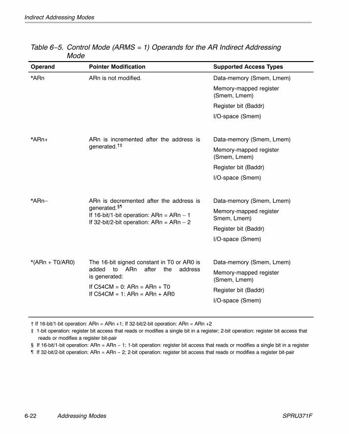
Indirect Addressing Modes
Addressing Modes6-22 SPRU371F
Table 6−5. Control Mode (ARMS = 1) Operands for the AR Indirect Addressing Mode
Operand Pointer Modification Supported Access Types
*ARn ARn is not modified. Data-memory (Smem, Lmem)
Memory-mapped register(Smem, Lmem)
Register bit (Baddr)
I/O-space (Smem)
*ARn+ ARn is incremented after the address isgenerated.†‡
Data-memory (Smem, Lmem)
Memory-mapped register(Smem, Lmem)
Register bit (Baddr)
I/O-space (Smem)
*ARn– ARn is decremented after the address isgenerated.§¶
If 16-bit/1-bit operation: ARn = ARn – 1If 32-bit/2-bit operation: ARn = ARn – 2
Data-memory (Smem, Lmem)
Memory-mapped register Smem, Lmem)
Register bit (Baddr)
I/O-space (Smem)
*(ARn + T0/AR0) The 16-bit signed constant in T0 or AR0 isadded to ARn after the addressis generated:
If C54CM = 0: ARn = ARn + T0If C54CM = 1: ARn = ARn + AR0
Data-memory (Smem, Lmem)
Memory-mapped register(Smem, Lmem)
Register bit (Baddr)
I/O-space (Smem)
† If 16-bit/1-bit operation: ARn = ARn +1; If 32-bit/2-bit operation: ARn = ARn +2‡ 1-bit operation: register bit access that reads or modifies a single bit in a register; 2-bit operation: register bit access that reads or modifies a register bit-pair§ If 16-bit/1-bit operation: ARn = ARn − 1; 1-bit operation: register bit access that reads or modifies a single bit in a register¶ If 32-bit/2-bit operation: ARn = ARn − 2; 2-bit operation: register bit access that reads or modifies a register bit-pair

Indirect Addressing Modes
6-23Addressing ModesSPRU371F
Table 6−5. Control Mode (ARMS = 1) Operands for the AR Indirect Addressing Mode (Continued)
Operand Supported Access TypesPointer Modification
*(ARn – T0/AR0) The 16-bit signed constant in T0 or AR0 issubtracted from ARn after the address isgenerated:If C54CM = 0: ARn = ARn – T0If C54CM = 1: ARn = ARn – AR0
Data-memory (Smem, Lmem)
Memory-mapped register(Smem, Lmem)
Register bit (Baddr)
I/O-space (Smem)
*ARn(T0/AR0) ARn is not modified. ARn is used as a basepointer. The 16-bit signed constant in T0 orAR0 is used as an offset from that basepointer:If C54CM = 0, T0 is usedIf C54CM = 1, AR0 is used
Data-memory (Smem, Lmem)
Memory-mapped register(Smem, Lmem)
Register bit (Baddr)
I/O-space (Smem)
*ARn(#K16) ARn is not modified. ARn is used as a basepointer. The 16-bit signed constant (K16) isused as an offset from that base pointer.
Note: When an instruction uses thisoperand, the constant is encoded in a 2-byteextension to the instruction. Because of theextension, an instruction using this operandcannot be executed in parallel with anotherinstruction.
Data-memory (Smem, Lmem)
Memory-mapped register(Smem, Lmem)
Register bit (Baddr)
† If 16-bit/1-bit operation: ARn = ARn +1; If 32-bit/2-bit operation: ARn = ARn +2‡ 1-bit operation: register bit access that reads or modifies a single bit in a register; 2-bit operation: register bit access that reads or modifies a register bit-pair§ If 16-bit/1-bit operation: ARn = ARn − 1; 1-bit operation: register bit access that reads or modifies a single bit in a register¶ If 32-bit/2-bit operation: ARn = ARn − 2; 2-bit operation: register bit access that reads or modifies a register bit-pair

Indirect Addressing Modes
Addressing Modes6-24 SPRU371F
Table 6−5. Control Mode (ARMS = 1) Operands for the AR Indirect Addressing Mode (Continued)
Operand Supported Access TypesPointer Modification
*+ARn(#K16) The 16-bit signed constant (K16) is added toARn before the address is generated:ARn = ARn + K16
Note: When an instruction uses thisoperand, the constant is encoded in a 2-byteextension to the instruction. Because of theextension, an instruction using this operandcannot be executed in parallel with anotherinstruction.
Data-memory (Smem, Lmem)
Memory-mapped register(Smem, Lmem)
Register bit (Baddr)
*ARn(short(#k3)) ARn is not modified. ARn is used as a basepointer. The 3-bit unsigned constant (k3) isused as an offset from that base pointer. k3is in the range 1 to 7.
Data-memory (Smem, Lmem)
Memory-mapped register(Smem, Lmem)
Register bit (Baddr)
I/O-space (Smem)
† If 16-bit/1-bit operation: ARn = ARn +1; If 32-bit/2-bit operation: ARn = ARn +2‡ 1-bit operation: register bit access that reads or modifies a single bit in a register; 2-bit operation: register bit access that reads or modifies a register bit-pair§ If 16-bit/1-bit operation: ARn = ARn − 1; 1-bit operation: register bit access that reads or modifies a single bit in a register¶ If 32-bit/2-bit operation: ARn = ARn − 2; 2-bit operation: register bit access that reads or modifies a register bit-pair

Indirect Addressing Modes
6-25Addressing ModesSPRU371F
Table 6−6. Summary of Indirect OperandsNot Modified Post Modified Premodified
AR Indirect, DSP Mode (ARMS = 0)
*ARn
*ARn(T0/AR0)
*ARn(T1)
*ARn(#K16)
*ARn+
*ARn−
*(ARn + T0/AR0)
*(ARn − T0/AR0)
*(ARn + T0B/AR0B)
*(ARn − T0B/AR0B)
*(ARn + T1)
*(ARn − T1)
*+ARn
*−ARn
*+ARn(#K16)
AR Indirect, Control Mode (ARMS = 1)
*ARn
*ARn(T0/AR0)
*ARn(#K16)
*ARn(short(#k3))
*ARn+
*ARn−
*(ARn + T0/AR0)
*(ARn − T0/AR0)
*(ARn + T0B/AR0B)
*(ARn − T0B/AR0B)
*(ARn + T1)
*(ARn − T1)
*+ARn(#K16)
6.4.2 Dual AR Indirect Addressing Mode
The dual AR indirect addressing mode enables you to make two data-memoryaccesses through the eight auxiliary registers, AR0–AR7. As with single ARindirect accesses to data space (see section 6.4.1.1), the CPU uses anextended auxiliary register to create each 23-bit address. You can use linearaddressing or circular addressing for each of the two accesses.
You may use the dual AR indirect addressing mode for:
� Executing an instruction that makes two 16-bit data-memory accesses. Inthis case, the two data-memory operands are designated in the instructionsyntax as Xmem and Ymem. For example:
ADD Xmem, Ymem, ACx

Indirect Addressing Modes
Addressing Modes6-26 SPRU371F
� Executing two instructions in parallel. In this case, both instructions musteach access a single memory value, designated in the instructionsyntaxes as Smem or Lmem. For example:
MOV Smem, dst|| AND Smem, src, dst
The operand of the first instruction is treated as an Xmem operand, andthe operand of the second instruction is treated as a Ymem operand.
The available dual AR indirect operands are a subset of the AR indirectoperands. The ARMS status bit does not affect the set of dual ARindirect operands available.
Note:
The assembler rejects code in which dual operands use the same auxiliaryregister with two different auxiliary register modifications. You can use the sameARn for both operands only if one of the operands does not modify ARn.
6.4.2.1 Dual AR Indirect Operands
Table 6−7 introduces the operands available for the dual AR indirectaddressing mode. Note that:
� Both pointer modification and address generation are linear or circularaccording to the pointer configuration in status register ST2_55. Thecontent of the appropriate 16-bit buffer start address register (BSA01,BSA23, BSA45, or BSA67) is added only if circular addressing is activatedfor the chosen pointer.
� Increments and decrements are made to the 16-bit pointer only. Youcannot address data across main data pages without changing the valuein the extension register (ARnH). To change ARnH, you must write to thefull 23−bit register, XARn.
Note:
Although an increment past FFFFh or a decrement past 0000h causes thepointer value to wrap around, do not make use of this behavior; it isnot supported. Also, during circular addressing, the BSAxx addition must notincrement the address beyond FFFFh.

Indirect Addressing Modes
6-27Addressing ModesSPRU371F
Table 6−7. Dual AR Indirect Operands Operand Pointer Modification Supported Access Type
*ARn ARn is not modified. Data-memory (Smem, Lmem, Xmem, Ymem)
*ARn+ ARn is incremented after theaddress is generated.†‡
Data-memory (Smem, Lmem, Xmem, Ymem)
*ARn– ARn is decremented after theaddress is generated.§¶
Data-memory (Smem, Lmem, Xmem, Ymem)
*(ARn + T0/AR0) The 16-bit signed constant in T0 orAR0 is added to ARn after theaddress is generated:If C54CM = 0: ARn = ARn + T0If C54CM = 1: ARn = ARn + AR0
Data-memory (Smem, Lmem, Xmem, Ymem)
*(ARn – T0/AR0) The 16-bit signed constant in T0 orAR0 is subtracted from ARn after theaddress is generated:If C54CM = 0: ARn = ARn – T0If C54CM = 1: ARn = ARn – AR0
Data-memory (Smem, Lmem, Xmem, Ymem)
*ARn(T0/AR0) ARn is not modified. ARn is used asa base pointer. The 16-bit signedconstant in T0 or AR0 is used as anoffset from that base pointer:If C54CM = 0, T0 is usedIf C54CM = 1, AR0 is used
Data-memory (Smem, Lmem, Xmem, Ymem)
*(ARn + T1) The 16-bit signed constant in T1 isadded to ARn after the addressis generated:ARn = ARn + T1
Data-memory (Smem, Lmem, Xmem, Ymem)
*(ARn – T1) The 16-bit signed constant in T1 issubtracted from ARn after theaddress is generated:ARn = ARn – T1
Data-memory (Smem, Lmem, Xmem, Ymem)
† If 16-bit operation: ARn = ARn + 1‡ If 32-bit operation: ARn = ARn + 2§ If 16-bit operation: ARn = ARn − 1¶ If 32-bit operation: ARn = ARn − 2

Indirect Addressing Modes
Addressing Modes6-28 SPRU371F
6.4.3 CDP Indirect Addressing Mode
This mode uses the coefficient data pointer (CDP) to point to data. As shownin Table 6−8, the way the CPU uses CDP to generate an address depends onthe access type.
Table 6−8. Use of the Coefficient Data Pointer (CDP) in the CDP Indirect Addressing Mode
For An Access To ... CDP Contains ...
Data space(memory or registers)
The 16 least significant bits (LSBs) of a 23-bit address.The 7 most significant bits (MSBs) are supplied byCDPH, the high part of the extended coefficient datapointer (XCDP). See section 6.4.3.1.
A register bit (or bit pair) A bit number. See section 6.4.3.2.
I/O space A 16-bit I/O address. See section 6.4.3.3.
6.4.3.1 CDP Indirect Accesses of Data Space
Figure 6−11 shows how the CPU generates data-space addresses for theCDP indirect addressing mode. (Note that both data memory andmemory-mapped registers are mapped to data space.) CDPH provides the7 most significant bits, and the coefficient data pointer (CDP) providesthe 16 least significant bits. The concatenation of CDPH and CDP is called theextended coefficient data pointer (XCDP).

Indirect Addressing Modes
6-29Addressing ModesSPRU371F
Figure 6−11.Accessing Data Space With the CDP Indirect Addressing Mode
1111 1111 1111 1111
Data space
Main page 0:
Main page 1:
Main page 2:
Main page 127:
000 0000
CDPCDPH
0000 0000 0000 0000
000 0000
.
.
.
.
.
.
.
.
.
.
.
.
.
.
.
.
.
.
..
.
..
.
..
. ...
..
.
..
.
..
. ...
01�0000h−01 FFFFh
02�0000h−02 FFFFh
7F�0000h−7F�FFFFh
.
.
.
.
.
.
00�0000h−00 FFFFh
000 0001 0000 0000 0000 0000
000 0001 1111 1111 1111 1111000 0010
000 0010
0000 0000 0000 0000
1111 1111 1111 1111
111 1111
111 1111
0000 0000 0000 0000
1111 1111 1111 1111
XCDP
6.4.3.2 CDP Indirect Accesses of Register Bits
When the CDP indirect addressing mode is used to access a register bit, CDPcontains the bit number. For example, if CDP contains 0, it points to bit 0, theleast significant bit (LSB) of the register.
Only the register bit test/set/clear/complement instructions supportCDP indirect accesses to register bits. These instructions enable you toaccess bits in the following registers only: the accumulators (AC0–AC3), theauxiliary registers (AR0–AR7), and the temporary registers (T0–T3).
Figure 6−12. Accessing Register Bits With the CDP Indirect Addressing Mode
CDP: M ... 11 10 9 8 7 6 5 4 3 2 1 0
...
MSB Register LSB
Note: Bit address M is 39 or 15, depending on the size of the register.

Indirect Addressing Modes
Addressing Modes6-30 SPRU371F
6.4.3.3 CDP Indirect Accesses of I/O Space
Words in I/O space are accessed at 16-bit addresses. When the CDP indirectaddressing mode is used to access I/O space, the 16-bit CDP contains thecomplete I/O address.
Figure 6−13. Accessing I/O Space With the CDP Indirect Addressing Mode
1111 1111 1111 1111
I/O spaceCDP
0000 0000 0000 0000...
0000h−FFFFh
6.4.3.4 CDP Indirect Operands
Table 6−9 introduces the operands available for the CDP indirect addressingmode. Note that:
� Both pointer modification and address generation are linear or circularaccording to the pointer configuration in status register ST2_55. Thecontent of the 16-bit buffer start address register BSAC is added only ifcircular addressing is activated for CDP.
� Increments and decrements are made to the 16-bit pointer only. Youcannot address data across main data pages without changing the valuein the extension register (CDPH).
Note:
Although an increment past FFFFh or a decrement past 0000h causes thepointer value to wrap around, do not make use of this behavior; it isnot supported. Also, during circular addressing, the BSAC addition must notincrement the address beyond FFFFh.

Indirect Addressing Modes
6-31Addressing ModesSPRU371F
Table 6−9. CDP Indirect Operands Operand Pointer Modification Supported Access Types
*CDP CDP is not modified. Data-memory(Smem, Lmem)
Memory-mapped register(Smem, Lmem)
Register-bit (Baddr)
I/O-space (Smem)
*CDP+ CDP is incremented after the address is generated.†‡ Data-memory(Smem, Lmem)
Memory-mapped register(Smem, Lmem)
Register-bit (Baddr)
I/O-space (Smem)
*CDP– CDP is decremented after the address is generated.§¶ Data-memory(Smem, Lmem)
Memory-mapped register(Smem, Lmem)
Register-bit (Baddr)
I/O-space (Smem)
*CDP(#K16) CDP is not modified. CDP is used as a base pointer. The16-bit signed constant (K16) is used as an offset from thatbase pointer.
Note: When an instruction uses this operand, the constantis encoded in a 2-byte extension to the instruction. Becauseof the extension, an instruction using this operand cannot beexecuted in parallel with another instruction.
Data-memory(Smem, Lmem)
Memory-mapped register(Smem, Lmem)
Register-bit (Baddr)
† If 16-bit/1-bit operation: CDP = CDP + 1; 1-bit operation: register bit access that reads or modifies a single bit in a register‡ If 32-bit/2-bit operation: CDP = CDP + 2; 2-bit operation: register bit access that reads or modifies a register bit pair§ If 16-bit/1-bit operation: CDP = CDP − 1; 1-bit operation: register bit access that reads or modifies a single bit in a register¶ If 32-bit/2-bit operation: CDP = CDP − 2; 2-bit operation: register bit access that reads or modifies a register bit pair

Indirect Addressing Modes
Addressing Modes6-32 SPRU371F
Table 6−9. CDP Indirect Operands (Continued)Operand Supported Access TypesPointer Modification
*+CDP(#K16) The 16-bit signed constant (K16) is added to CDP before theaddress is generated: CDP = CDP + K16
Note: When an instruction uses this operand, the constantis encoded in a 2-byte extension to the instruction. Becauseof the extension, an instruction using this operand cannot beexecuted in parallel with another instruction.
Data-memory(Smem, Lmem)
Memory-mapped register(Smem, Lmem)
Register-bit (Baddr)
† If 16-bit/1-bit operation: CDP = CDP + 1; 1-bit operation: register bit access that reads or modifies a single bit in a register‡ If 32-bit/2-bit operation: CDP = CDP + 2; 2-bit operation: register bit access that reads or modifies a register bit pair§ If 16-bit/1-bit operation: CDP = CDP − 1; 1-bit operation: register bit access that reads or modifies a single bit in a register¶ If 32-bit/2-bit operation: CDP = CDP − 2; 2-bit operation: register bit access that reads or modifies a register bit pair
6.4.4 Coefficient Indirect Addressing Mode
This mode uses the same address-generation process as the CDP indirectaddressing mode for data-space accesses. The coefficient indirectaddressing mode is supported by select memory move/initialization syntaxesand by the following arithmetical instructions:
� Finite impulse response filter� Multiply� Multiply and accumulate� Multiply and subtract� Dual multiply [and accumulate/subtract]
Instructions using the coefficient indirect addressing mode to access data aremainly instructions performing operations with three memory operands percycle. Two of these operands (Xmem and Ymem) are accessed with the dualAR indirect addressing mode. The third operand (Cmem) is accessed with thecoefficient indirect addressing mode. The Cmem operand is carried onthe BB bus of the CPU (see section 1.6, Address Buses and Data Buses).
Consider the following instruction syntax. In one cycle, two multiplications canbe performed in parallel. One memory operand (Cmem) is common to bothmultiplications, while dual AR indirect operands (Xmem and Ymem) are usedfor the other values in the multiplication.
MPY Xmem, Cmem, ACx:: MPY Ymem, Cmem, ACy
To access three memory values (as in the above example) in a single cycle,the value referenced by Cmem must be located in a memory bank differentfrom the one containing the Xmem and Ymem values.

Indirect Addressing Modes
6-33Addressing ModesSPRU371F
6.4.4.1 Important Facts About the BB Bus
Keep the following facts about the BB bus in mind as you use the coefficientindirect addressing mode:
� Although the following instructions access Cmem operands, they do notuse the BB bus to fetch the 16-bit or 32-bit Cmem operand.
InstructionSyntax
Description ofCmem Access
Bus Used toAccess Cmem
MOV Cmem, Smem 16-bit read from Cmem DB
MOV Smem, Cmem 16-bit write to Cmem EB
MOV Cmem, dbl(Lmem) 32-bit read from Cmem CB for most significantword (MSW)DB for least significantword (LSW)
MOV dbl(Lmem), Cmem 32-bit write to Cmem FB for MSWEB for LSW
� The BB bus is not connected to external memory. If a Cmem operand isaccessed via BB, the operand must be in internal memory.
6.4.4.2 Coefficient Indirect Operands
Table 6−10 introduces the operands available for the coefficient indirectaddressing mode. Note that:
� Both pointer modification and address generation are linear or circularaccording to the pointer configuration in status register ST2_55. Thecontent of the 16-bit buffer start address register BSAC is added only ifcircular addressing is activated for CDP.

Indirect Addressing Modes
Addressing Modes6-34 SPRU371F
� Increments and decrements are made to the 16-bit pointer only. Youcannot address data across main data pages without changing the valuein the extension register (CDPH).
Notes:
1) Although an increment past FFFFh or a decrement past 0000h causesthe pointer value to wrap around, do not make use of this behavior; it isnot supported. Also, during circular addressing, the BSAC addition mustnot increment the address beyond FFFFh.
2) If you use algebraic instructions, you must enclose each coefficientindirect operand in the syntax element coef() (see section 6.4.4.3). If youuse mnemonic instructions, you can use the operands as shown inTable 6−10.
Table 6−10. Coefficient Indirect OperandsOperand Pointer Modification Supported Access Type
*CDP CDP is not modified. Data-memory
*CDP+ CDP is incremented after the address isgenerated:If 16-bit operation: CDP = CDP + 1If 32-bit operation: CDP = CDP + 2
Data-memory
*CDP– CDP is decremented after the address isgenerated:If 16-bit operation: CDP = CDP – 1If 32-bit operation: CDP = CDP – 2
Data-memory
*(CDP + T0/AR0) The 16-bit signed constant in T0 or AR0 isadded to CDP after the address isgenerated:If C54CM = 0: CDP = CDP + T0If C54CM = 1: CDP = CDP + AR0
Data-memory
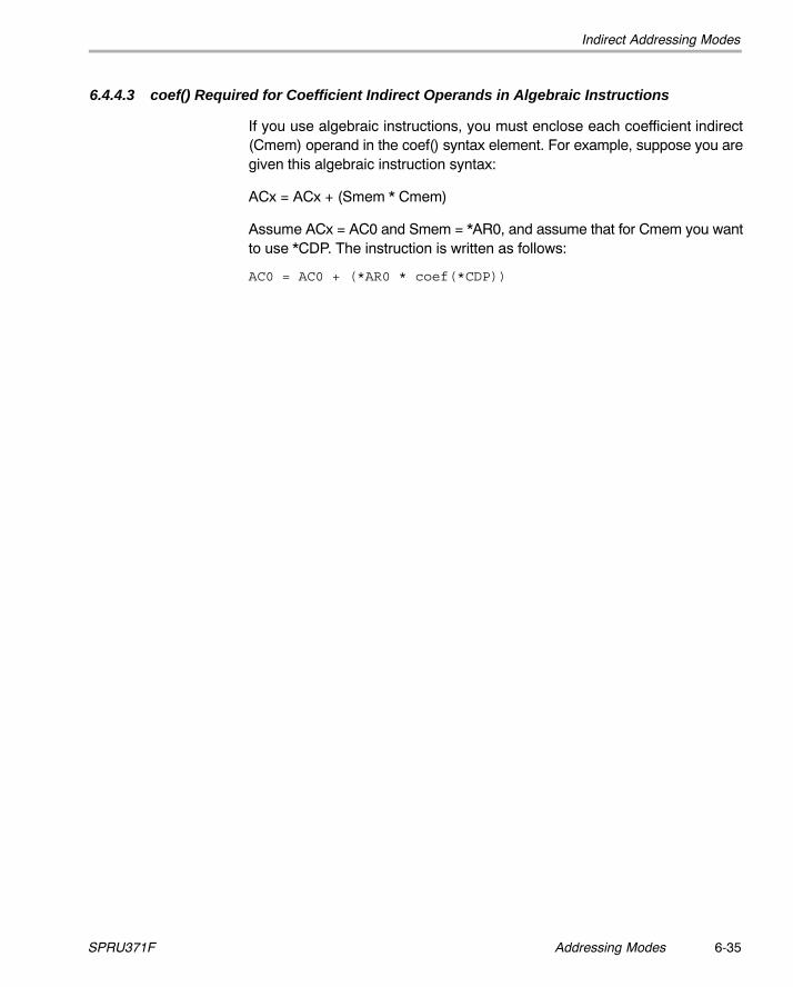
Indirect Addressing Modes
6-35Addressing ModesSPRU371F
6.4.4.3 coef() Required for Coefficient Indirect Operands in Algebraic Instructions
If you use algebraic instructions, you must enclose each coefficient indirect(Cmem) operand in the coef() syntax element. For example, suppose you aregiven this algebraic instruction syntax:
ACx = ACx + (Smem * Cmem)
Assume ACx = AC0 and Smem = *AR0, and assume that for Cmem you wantto use *CDP. The instruction is written as follows:
AC0 = AC0 + (*AR0 * coef(*CDP))

Addressing Data Memory
Addressing Modes6-36 SPRU371F
6.5 Addressing Data Memory
Absolute, direct, and indirect addressing can be used to address values in datamemory:
Addressing Type See ...
Absolute This page
Direct Page 6-37
Indirect Page 6-38
6.5.1 Addressing Data Memory With Absolute Addressing Modes
The k16 absolute operand *abs16(#k16) or the k23 absolute operand *(#k23)can be used to access data memory in any instruction with one of these syntaxelements:
Smem Indicates one word (16 bits) of data
Lmem Indicates two adjacent words (32 bits) of data
Table 6−11 and Table 6−12 provide examples of how to use these operands.
Note:
Because of a multi-byte extension, an instruction using *abs16(#k16) or*(#k23) cannot be executed in parallel with another instruction.
� When an instruction uses *abs16(#k16), the constant, k16, is encodedin a 2-byte extension to the instruction.
� When an instruction uses *(#k23), the constant, k23, is encoded in a3-byte extension to the instruction.
Table 6−11. *abs16(#k16) Used for Data-Memory Access
Example Syntax Example InstructionAddress(es) GeneratedFor DPH = 3 Description
MOV Smem, dst MOV *abs16(#2002h), T2 DPH:k16 = 03 2002h The CPU loads thevalue at address03 2002h into T2.
MOV dbl(Lmem), pair(TAx) MOV dbl(*abs16(#2002h)), pair(T2) DPH:k16 = 03 2002h(DPH:k16) + 1 = 03 2003h
The CPU reads thevalues at addresses03 2002h and03 2003h and copiesthem into T2 and T3,respectively.

Addressing Data Memory
6-37Addressing ModesSPRU371F
Table 6−12. *(#k23) Used for Data-Memory Access
Example Syntax Example Instruction Address(es) Generated Description
MOV Smem, dst MOV *(#032002h), T2 k23 = 03 2002h The CPU loads the value ataddress 03 2002h into T2.
MOV dbl(Lmem), pair(TAx) MOV dbl(*(#032002h)), pair(T2) k23 = 03 2002hk23 + 1 = 03 2003h
The CPU reads the valuesat address 03 2002hand address 03 2003h andcopies them into T2 and T3,respectively.
6.5.2 Addressing Data Memory With Direct Addressing Modes
You can use direct addressing modes to access data memory in anyinstruction with one of these syntax elements:
Smem Indicates one word (16 bits) of data
Lmem Indicates two adjacent words (32 bits) of data
When the CPL bit is 0, you can use the DP direct operand (@Daddr). Whenthe CPL bit is 1, you can use the SP direct operand *SP(offset). Table 6−13 andTable 6−14 provide examples of using these operands to access datamemory.
For the DP direct addressing mode, the assembler calculates Doffset for theaddress as follows:
Doffset = (Daddr – .dp) & 7Fh
where .dp is a value assigned by the .dp assembler directive, and & indicatesa bitwise AND operation. For examples of using the .dp directive and of theDoffset calculation, see section 6.3.1.1. As shown in Table 6−13, whenDP = .dp, Doffset is equal to Daddr (in this case, both are 0005h).

Addressing Data Memory
Addressing Modes6-38 SPRU371F
Table 6−13. @Daddr Used for Data-Memory Access
Example Syntax Example InstructionAddress(es) GeneratedFor DPH = 3, DP = .dp = 0 Description
MOV Smem, dst MOV @0005h, T2 DPH:(DP + Doffset)= 03:(0000h + 0005h)= 03 0005h
The CPU loads thevalue at address03 0005h into T2.
MOV dbl(Lmem), pair(TAx) MOV dbl(@0005h),pair(T2)
DPH:(DP + Doffset) = 03 0005hDPH:(DP + Doffset – 1) = 03 0004h
The CPU reads thevalues at addresses03 0005h and03 0004h and loadsthese values into T2and T3, respectively.The second word isread from the precedingeven address inaccordance with thealignment rule for longwords.
Table 6−14. *SP(offset) Used for Data-Memory Access
Example Syntax Example InstructionAddress(es) GeneratedFor SP = FF00h and SPH = 0 Description
MOV Smem, dst MOV *SP(5), T2 SPH:(SP + offset) = 00 FF05h The CPU loads thevalue at address00 FF05h into T2.
MOV dbl(Lmem), pair(TAx) MOV dbl(*SP(5)),pair(T2)
SPH:(SP + offset) = 00 FF05hSPH:(SP + offset – 1) = 00 FF04h
The CPU reads thevalues at addresses00 FF05h and00 FF04h, and loadsthese values into T2and T3, respectively.The second word isread from the precedingeven address inaccordance with thealignment rule for longwords.
6.5.3 Addressing Data Memory With Indirect Addressing Modes
When you want to use indirect operands to access data memory, it is importantto know which operands you can use for a given instruction. Each instructionsyntax that supports indirect accesses to data memory includes one of thesyntax elements shown in Table 6−15. The last column of the table showswhich indirect operands can be used in place of the syntax element(s) foraccesses to data memory. As explained in section 6.4.1.4, the AR indirect

Addressing Data Memory
6-39Addressing ModesSPRU371F
operands available depend on whether DSP mode or control mode is selectedby the ARMS bit. After you have found an operand in Table 6−15, you can finddetails about that operand in the sections that follow the table. For detailsabout the alignment of long words in data memory, see section 3.3.2,Data Types.
Table 6−15. Choosing an Indirect Operand for a Data Memory Access
Syntax Element Description Available Indirect Operands
Smem or Lmem Smem indicates one word (16 bits) ofdata. Lmem indicates two consecutivewords (32 bits) of data.
AR indirect addressing mode:DSP mode (ARMS = 0): Control mode (ARMS = 1):*ARn *ARn*ARn+ *ARn+*ARn− *ARn−*+ARn*−ARn*(ARn + T0/AR0) *(ARn + T0/AR0)*(ARn − T0/AR0) *(ARn − T0/AR0)*ARn(T0/AR0) *ARn(T0/AR0)*(ARn + T0B/AR0B)*(ARn − T0B/AR0B)*(ARn + T1)*(ARn − T1)*ARn(T1)*ARn(#K16) *ARn(#K16)*+ARn(#K16) *+ARn(#K16)
*ARn(short(#k3))
CDP indirect addressing mode:*CDP*CDP+*CDP−*CDP(#k16)*+CDP(#k16)
Xmem or Ymem One word (16 bits) of data Dual AR indirect addressing mode:*ARn*ARn+*ARn−*(ARn + T0/AR0)*(ARn − T0/AR0)*ARn(T0/AR0)*(ARn + T1)*(ARn − T1)
Cmem One word (16 bits) of data Coefficient indirect addressing mode:*CDP*CDP+*CDP−*(CDP + T0/AR0)

Addressing Data Memory
Addressing Modes6-40 SPRU371F
6.5.3.1 *ARn Used for Data-Memory Access
Operand Description
*ARn Address generated:ARnH:( [BSAyy +] ARn)
ARn is not modified.
Example Syntax Example InstructionAddress(es) Generated(Linear Addressing) Description
MOV Smem, dst MOV *AR4, T2 AR4H:AR4 = XAR4 The CPU reads the value at addressXAR4 and loads it into T2. AR4 is notmodified.
MOV dbl(Lmem), pair(TAx) MOV dbl(*AR4), pair(T2) First address:XAR4
Second address:If XAR4 is even XAR4 + 1If XAR4 is odd XAR4 – 1
The CPU reads the values ataddress XAR4 and the following orpreceding address, and loads theminto T2 and T3, respectively. AR4 isnot modified.
For details about the alignment oflong words in data memory, seeData Types on page 3-5.
6.5.3.2 *ARn+ Used for Data-Memory Access
Operand Description
*ARn+ 1) Address generated:ARnH:( [BSAyy +] ARn)
2) ARn modified:If 16-bit operation: ARn = ARn + 1If 32-bit operation: ARn = ARn + 2
Example Syntax Example InstructionAddress(es) Generated(Linear Addressing) Description
MOV Smem, dst MOV *AR4+, T2 AR4H:AR4 = XAR4 The CPU reads the value ataddress XAR4 and loads it intoT2. After being used for theaddress, AR4 is incrementedby 1.
MOV dbl(Lmem), pair(TAx) MOV dbl(*AR4+), pair(T2) First address:XAR4
Second address:If XAR4 is even XAR4 + 1If XAR4 is odd XAR4 – 1
The CPU reads the values ataddress XAR4 and the followingor preceding address, and loadsthem into T2 and T3, respectively.After being used for theaddresses, AR4 is incrementedby 2.
For details about the alignment oflong words in data memory, seeData Types on page 3-5.

Addressing Data Memory
6-41Addressing ModesSPRU371F
6.5.3.3 *ARn– Used for Data-Memory Access
Operand Description
*ARn– 1) Address generated:ARnH:( [BSAyy +] ARn)
2) ARn modified:If 16-bit operation: ARn = ARn – 1If 32-bit operation: ARn = ARn – 2
Example Syntax Example InstructionAddress(es) Generated(Linear Addressing) Description
MOV Smem, dst MOV *AR4–, T2 AR4H:AR4 = XAR4 The CPU reads the value at addressXAR4 and loads it into T2. After beingused for the address, AR4 isdecremented by 1.
MOV dbl(Lmem), pair(TAx) MOV dbl(*AR4–), pair(T2) First address:XAR4
Second address:If XAR4 is even XAR4 + 1If XAR4 is odd XAR4 – 1
The CPU reads the values ataddress XAR4 and the following orpreceding address, and loads theminto T2 and T3, respectively. Afterbeing used for the addresses, AR4 isdecremented by 2.
For details about the alignment oflong words in data memory, see DataTypes on page 3-5.

Addressing Data Memory
Addressing Modes6-42 SPRU371F
6.5.3.4 *+ARn Used for Data-Memory Access
Operand Description
*+ARn 1) ARn modified:If 16-bit operation: ARn = ARn + 1If 32-bit operation: ARn = ARn + 2
2) Address generated:If 16-bit operation: ARnH:( [BSAyy +] ARn + 1)If 32-bit operation: ARnH:( [BSAyy +] ARn + 2)
Example Syntax Example InstructionAddress(es) Generated(Linear Addressing) Description
MOV Smem, dst MOV *+AR4, T2 AR4H:(AR4 + 1)= XAR4 + 1
Before being used for theaddress, AR4 is incremented by1. The CPU reads the value ataddress XAR4 + 1 and loads itinto T2.
MOV dbl(Lmem), pair(TAx) MOV dbl(*+AR4), pair(T2) First address:AR4H:(AR4 + 2)= XAR4 + 2
Second address:If XAR4 + 2 is even (XAR4 + 2) + 1If XAR4 + 2 is odd (XAR4 + 2) – 1
Before being used for theaddresses, AR4 is incrementedby 2. The CPU reads the valuesat address XAR4 + 2 and thefollowing or preceding address,and loads them into T2 and T3,respectively.
For details about the alignmentof long words in data memory,see Data Types on page 3-5.

Addressing Data Memory
6-43Addressing ModesSPRU371F
6.5.3.5 *–ARn Used for Data-Memory Access
Operand Description
*–ARn 1) ARn modified:If 16-bit operation: ARn = ARn – 1If 32-bit operation: ARn = ARn – 2
2) Address generated:If 16-bit operation: ARnH:( [BSAyy +] ARn – 1)If 32-bit operation: ARnH:( [BSAyy +] ARn – 2)
Example Syntax Example InstructionAddress(es) Generated(Linear Addressing) Description
MOV Smem, dst MOV *–AR4, T2 AR4H:(AR4 – 1)= XAR4 – 1
Before being used for theaddress, AR4 is decremented by1. The CPU reads the value ataddress XAR4 – 1 and loads itinto T2.
MOV dbl(Lmem), pair(TAx) MOV dbl(*–AR4), pair(T2) First address:AR4H:(AR4 – 2)= XAR4 – 2
Second address:If XAR4 – 2 is even (XAR4 – 2) + 1If XAR4 – 2 is odd (XAR4 – 2) – 1
Before being used for theaddresses, AR4 is decrementedby 2. The CPU reads the values ataddress XAR4 – 2 and thefollowing or preceding addressand loads them into T2 and T3,respectively.
For details about the alignment oflong words in data memory, seeData Types on page 3-5.

Addressing Data Memory
Addressing Modes6-44 SPRU371F
6.5.3.6 *(ARn + T0/AR0) Used for Data-Memory Access
C54CM = 0 C54CM = 1
Operand Description Operand Description
*(ARn + T0) 1) Address generated:ARnH:( [BSAyy +] ARn)
2) ARn modified:ARn = ARn + T0
*(ARn + AR0) 1) Address generated:ARnH:( [BSAyy +] ARn)
2) ARn modified:ARn = ARn + AR0
Example Syntax Example Instruction
Address(es)Generated(Linear Addressing) Description
MOV Smem, dst MOV *(AR4 + T0), T2 AR4H:AR4 = XAR4 The CPU reads the value ataddress XAR4 and loads itinto T2. After being used forthe address, AR4 isincremented by the numberin T0.
MOV dbl(Lmem), pair(TAx) MOV dbl(*(AR4 + T0)), pair(T2) First address:XAR4
Second address:If XAR4 is even XAR4 + 1If XAR4 is odd XAR4 – 1
The CPU reads the values ataddress XAR4 and thefollowing or precedingaddress and loads them intoT2 and T3, respectively. Afterbeing used for theaddresses, AR4 isincremented by the numberin T0.
For details about thealignment of long words indata memory, see DataTypes on page 3-5.

Addressing Data Memory
6-45Addressing ModesSPRU371F
6.5.3.7 *(ARn – T0/AR0) Used for Data-Memory Access
C54CM = 0 C54CM = 1
Operand Description Operand Description
*(ARn – T0) 1) Address generated:ARnH:( [BSAyy +] ARn)
2) ARn modified:ARn = ARn – T0
*(ARn – AR0) 1) Address generated:ARnH:( [BSAyy +] ARn)
2) ARn modified:ARn = ARn – AR0
Example Syntax Example Instruction
Address(es)Generated(Linear Addressing) Description
MOV Smem, dst MOV *(AR4 – T0), T2 AR4H:AR4 = XAR4 The CPU reads the value ataddress XAR4 and loads itinto T2. After being used forthe address, AR4 isdecremented by the numberin T0.
MOV dbl(Lmem), pair(TAx) MOV dbl(*(AR4 – T0)), pair(T2) First address:XAR4
Second address:If XAR4 is even XAR4 + 1If XAR4 is odd XAR4 – 1
The CPU reads the values ataddress XAR4 and thefollowing or precedingaddress, and loads them intoT2 and T3, respectively. Afterbeing used for theaddresses, AR4 isdecremented by the numberin T0.
For details about thealignment of long words indata memory, see DataTypes on page 3-5.

Addressing Data Memory
Addressing Modes6-46 SPRU371F
6.5.3.8 *ARn(T0/AR0) Used for Data-Memory Access
C54CM = 0 C54CM = 1
Operand Description Operand Description
*ARn(T0) Address generated:ARnH:( [BSAyy +] ARn + T0)
ARn is not modified. ARn isused as a base pointer. T0 isused as an offset from that basepointer.
*ARn(AR0) Address generated:ARnH:( [BSAyy +] ARn + AR0)
ARn is not modified. ARn isused as a base pointer. AR0is used as an offset from thatbase pointer.
Example Syntax Example InstructionAddress(es) Generated(Linear Addressing) Description
MOV Smem, dst MOV *AR4(T0), T2 AR4H:(AR4 + T0)= XAR4 + T0
The CPU reads the value ataddress XAR4 + T0 andloads it into T2. AR4 is notmodified.
MOV dbl(Lmem), pair(TAx) MOV dbl(*AR4(T0)), pair(T2) First address:XAR4 + T0
Second address:If XAR4 + T0 is even (XAR4 + T0) + 1If XAR4 + T0 is odd (XAR4 + T0) – 1
The CPU reads the values ataddress XAR4 + T0 and thefollowing or precedingaddress, and loads them intoT2 and T3, respectively. AR4is not modified.
For details about thealignment of long words indata memory, see DataTypes on page 3-5.

Addressing Data Memory
6-47Addressing ModesSPRU371F
6.5.3.9 *(ARn + T0B/AR0B) Used for Data-Memory Access
C54CM = 0 C54CM = 1
Operand Description Operand Description
*(ARn + T0B) 1) Address generated:ARnH:( [BSAyy +] ARn)
2) ARn modified:ARn = ARn + T0(done with reverse carrypropagation)
See Note about circularaddressing restriction.
*(ARn + AR0B) 1) Address generated:ARnH:( [BSAyy +] ARn)
2) ARn modified:ARn = ARn + AR0(done with reverse carrypropagation)
See Note about circularaddressing restriction.
Note: When this bit-reverse operand is used, ARn cannot be used as a circular pointer. If ARn is configured in ST2_55 forcircular addressing, the corresponding buffer start address register value (BSAyy) is added to ARn, but ARn is notmodified so as to remain inside a circular buffer.
Example Syntax Example Instruction
Address(es)Generated(Linear Addressing) Description
MOV Smem, dst MOV *(AR4 + T0B), T2 AR4H:AR4 = XAR4 The CPU reads the value ataddress XAR4 and loads it intoT2. After being used for theaddress, AR4 is incremented bythe number in T0. Reverse carrypropagation is used during theaddition.
MOV dbl(Lmem), pair(TAx) MOV dbl(*(AR4 + T0B)), pair(T2) First address:XAR4
Second address:If XAR4 is even XAR4 + 1If XAR4 is odd XAR4 – 1
The CPU reads the values ataddress XAR4 and the followingor preceding address and loadsthem into T2 and T3,respectively. After being usedfor the address, AR4 isincremented by the number inT0. Reverse carry propagationis used during the addition.
For details about the alignmentof long words in data memory,see Data Types on page 3-5.

Addressing Data Memory
Addressing Modes6-48 SPRU371F
6.5.3.10 *(ARn – T0B/AR0B) Used for Data-Memory Access
C54CM = 0 C54CM = 1
Operand Description Operand Description
*(ARn – T0B) 1) Address generated:ARnH:( [BSAyy +] ARn)
2) ARn modified:ARn = ARn – T0(done with reverse carrypropagation)
See Note about circularaddressing restriction.
*(ARn – AR0B) 1) Address generated:ARnH:( [BSAyy +] ARn)
2) ARn modified:ARn = ARn – AR0(done with reverse carrypropagation)
See Note about circularaddressing restriction.
Note: When this bit-reverse operand is used, ARn cannot be used as a circular pointer. If ARn is configured in ST2_55 forcircular addressing, the corresponding buffer start address register value (BSAyy) is added to ARn, but ARn is notmodified so as to remain inside a circular buffer.
Example Syntax Example InstructionAddress(es)Generated(Linear Addressing)
Description
MOV Smem, dst MOV *(AR4 – T0B), T2 AR4H:AR4 = XAR4 The CPU loads the value ataddress XAR4 into T2. Afterbeing used for the address,AR4 is decremented by thenumber in T0. Reversecarry propagation is usedduring the subtraction.
MOV dbl(Lmem), pair(TAx) MOV dbl(*(AR4 – T0B)), pair(T2) First address:XAR4
Second address:If XAR4 is even XAR4 + 1If XAR4 is odd XAR4 – 1
The CPU reads the valuesat address XAR4 and thefollowing or precedingaddress and loads them intoT2 and T3, respectively.After being used for theaddresses, AR4 isdecremented by the numberin T0. Reverse carrypropagation is used duringthe subtraction.
For details about thealignment of long words indata memory, see DataTypes on page 3-5.

Addressing Data Memory
6-49Addressing ModesSPRU371F
6.5.3.11 *(ARn + T1) Used for Data-Memory Access
Operand Description
*(ARn + T1) 1) Address generated:ARnH: [BSAyy +] ARn
2) ARn modified:ARn = ARn + T1
Example Syntax Example Instruction
Address(es)Generated(Linear Addressing) Description
MOV Smem, dst MOV *(AR7 + T1), AR3 AR7H:AR7 = XAR7 The CPU reads the value ataddress XAR7 and loads it intoAR3. After being used for theaddress, AR7 is incrementedby the number in T1.
MOV dbl(Lmem), pair(TAx) MOV dbl(*(AR5 + T1)), pair(AR2) First address:AR5H:AR5 = XAR5
Second address:If XAR5 is even XAR5 + 1If XAR5 is odd XAR5 – 1
The CPU reads the values ataddress XAR5 and thefollowing or precedingaddress, and loads them intoAR2 and AR3, respectively.After being used for theaddresses, AR5 isincremented by the number inT1.
For details about the alignmentof long words in data memory,see Data Types on page 3-5.

Addressing Data Memory
Addressing Modes6-50 SPRU371F
6.5.3.12 *(ARn – T1) Used for Data-Memory Access
Operand Description
*(ARn – T1) 1) Address generated:ARnH:( [BSAyy +] ARn)
2) ARn modified:ARn = ARn – T1
Example Syntax Example Instruction
Address(es)Generated(Linear Addressing) Description
MOV Smem, dst MOV *(AR7 – T1), AR3 AR7H:AR7 = XAR7 The CPU reads the value ataddress XAR7 and loads it intoAR3. After being used for theaddress, AR7 is decrementedby the number in T1.
MOV dbl(Lmem), pair(TAx) MOV dbl(*(AR5 – T1)), pair(AR2) First address:AR5H:AR5 = XAR5
Second address:If XAR5 is even XAR5 + 1If XAR5 is odd XAR5 – 1
The CPU reads the values ataddress XAR5 and thefollowing or preceding addressand loads them into AR2 andAR3, respectively. After beingused for the addresses, AR5 isdecremented by the number inT1.
For details about the alignmentof long words in data memory,see Data Types on page 3-5.
Addressing Data Memory
6-51Addressing ModesSPRU371F
6.5.3.13 *ARn(T1) Used for Data-Memory Access
Operand Description
*ARn(T1) Address generated:ARnH:( [BSAyy +] ARn + T1)
ARn is not modified. ARn is used as a base pointer. T1 is used as an offset from that basepointer.
Example Syntax Example Instruction
Address(es)Generated(Linear Addressing) Description
MOV Smem, dst MOV *AR7(T1), AR3 AR7H:(AR7 + T1)= XAR7 + T1
The CPU reads the value ataddress XAR7 + T1 and loads itinto AR3. AR7 is not modified.
MOV dbl(Lmem), pair(TAx) MOV dbl(*AR5(T1)), pair(AR2) First address:AR5H:(AR5 + T1)= XAR5 + T1
Second address:If XAR5 + T1 is even (XAR5 + T1) + 1If XAR5 + T1 is odd (XAR5 + T1) – 1
The CPU reads the values ataddress XAR5 + T1 and thefollowing or preceding address,and loads them into AR2 andAR3, respectively. AR5 is notmodified.
For details about the alignmentof long words in data memory,see Data Types on page 3-5.
6.5.3.14 *ARn(#K16) Used for Data-Memory Access
Operand Description
*ARn(#K16) Address generated:ARnH:( [BSAyy +] ARn + K16)
ARn is not modified. ARn is used as a base pointer. The 16-bit signed constant (K16) is used asan offset from that base pointer.
Note: When an instruction uses this operand, the constant, K16, is encoded in a 2-byte extension to the instruction. Because ofthe extension, an instruction using this operand cannot be executed in parallel with another instruction.
Example Syntax Example Instruction
Address(es)Generated(Linear Addressing) Description
MOV Smem, dst MOV *AR7(#8), AR3 AR7H:(AR7 + 8)= XAR7 + 8
The CPU reads the value ataddress XAR7 + 8 and loads itinto AR3. AR7 is not modified.
MOV dbl(Lmem), pair(TAx) MOV dbl(*AR5(#20)), pair(AR2) First address:AR5H:(AR5 + 20)= XAR5 + 20
Second address:If XAR5 + 20 is even (XAR5 + 20) + 1If XAR5 + 20 is odd (XAR5 + 20) – 1
The CPU reads the values ataddress XAR5 + 20 and thefollowing or preceding address,and loads them into AR2 andAR3, respectively. AR5 is notmodified.
For details about the alignmentof long words in data memory,see Data Types on page 3-5.

Addressing Data Memory
Addressing Modes6-52 SPRU371F
6.5.3.15 *+ARn(#K16) Used for Data-Memory Access
Operand Description
*+ARn(#K16) 1) ARn modified:ARn = ARn + K16
2) Address generated:ARnH:( [BSAyy +] ARn + K16)
Note: When an instruction uses this operand, the constant, K16, is encoded in a 2-byte extension to the instruction. Because ofthe extension, an instruction using this operand cannot be executed in parallel with another instruction.
Example Syntax Example Instruction
Address(es)Generated(Linear Addressing) Description
MOV Smem, dst MOV *+AR7(#8), AR3 AR7H:(AR7 + 8)= XAR7 + 8
Before AR7 is used for theaddress, the constant is addedto AR7. The CPU reads thevalue at address XAR7 + 8and loads it into AR3.
MOV dbl(Lmem), pair(TAx) MOV dbl(*+AR5(#20)), pair(AR2) First address:AR5H:(AR5 + 20)= XAR5 + 20
Second address:If XAR5 + 20 is even (XAR5 + 20) + 1If XAR5 + 20 is odd (XAR5 + 20) – 1
Before AR5 is used for theaddresses, the constant isadded to AR5. The CPU readsthe values at addressXAR5 + 20 and the followingor preceding address, andloads them into AR2 and AR3,respectively.
For details about the alignmentof long words in data memory,see Data Types on page 3-5.

Addressing Data Memory
6-53Addressing ModesSPRU371F
6.5.3.16 *ARn(short(#k3)) Used for Data-Memory Access
Operand Description
*ARn(short(#k3)) Address generated:ARnH:( [BSAyy +] ARn + k3)
ARn is not modified. ARn is used as a base pointer. The 3-bit unsigned constant (k3) is used asan offset from that base pointer. k3 can be a number from 1 to 7.
Example Syntax Example Instruction
Address(es)Generated(Linear Addressing) Description
MOV Smem, dst MOV *AR7(short(#1)), AR3 AR7H:(AR7 + 1)= XAR7 + 1
The CPU reads the valueat address XAR7 + 1 andloads it into AR3. AR7 isnot modified.
MOV dbl(Lmem), pair(TAx) MOV dbl(*AR5(short(#7))), pair(AR2) First address:AR5H:(AR5 + 7)= XAR5 + 7
Second address:If XAR5 + 7 is even (XAR5 + 7) + 1If XAR5 + 7 is odd (XAR5 + 7) – 1
The CPU reads the valuesat address XAR5 + 7 andthe following or precedingaddress, and loads theminto AR2 and AR3,respectively. AR5 is notmodified.
For details about thealignment of long words indata memory, see DataTypes on page 3-5.

Addressing Data Memory
Addressing Modes6-54 SPRU371F
6.5.3.17 *CDP Used for Data-Memory Access
Operand Description
*CDP Address generated:CDPH:[BSAC +] CDP
CDP is not modified.
Example Syntax Example Instruction
Address(es)Generated(Linear Addressing) Description
MOV Smem, dst MOV *CDP, T2 CDPH:CDP = XCDP The CPU reads the value at addressXCDP and loads it into T2. CDP isnot modified.
MOV dbl(Lmem), pair(TAx) MOV dbl(*CDP), pair(T2) First address:XCDP
Second address:If XCDP is even XCDP + 1If XCDP is odd XCDP – 1
The CPU reads the values ataddress XCDP and the following orpreceding address, and loads theminto T2 and T3, respectively. CDP isnot modified.
For details about the alignment oflong words in data memory, seeData Types on page 3-5.
MPY Xmem, Cmem, ACx:: MPY Ymem, Cmem, ACy
MPY *AR0, *CDP, AC0:: MPY *AR1, *CDP, AC1
CDPH:CDP = XCDP The CPU multiplies the value ataddress XAR0 by the coefficientat address XCDP and stores theresult to AC0. At the same time,the CPU multiplies the value ataddress XAR1 by the samecoefficient and stores the result toAC1. CDP is not modified.
MOV dbl(Lmem), Cmem MOV dbl(*AR7), *CDP First address:XCDP
Second address:If XCDP is even XCDP + 1If XCDP is odd XCDP – 1
The CPU reads the values ataddresses XAR7 and XAR7 ± 1.Then it writes the values toaddresses XCDP and XCDP ± 1,respectively. CDP is not modified.
Note: If you use algebraic instructions, you must enclose each coefficient indirect (Cmem) operand in the syntax elementcoef(). For an example, see section 6.4.4.3.

Addressing Data Memory
6-55Addressing ModesSPRU371F
6.5.3.18 *CDP+ Used for Data-Memory Access
Operand Description
*CDP+ 1) Address generated:CDPH:[BSAC +] CDP
2) CDP modified:If 16-bit operation: CDP = CDP + 1If 32-bit operation: CDP = CDP + 2
Example Syntax Example Instruction
Address(es)Generated(Linear Addressing) Description
MOV Smem, dst MOV *CDP+, T2 CDPH:CDP = XCDP The CPU reads the value at addressXCDP and loads it into T2. Afterbeing used for the address, CDP isincremented by 1.
MOV dbl(Lmem), pair(TAx) MOV dbl(*CDP+), pair(T2) First address:XCDP
Second address:If XCDP is even XCDP + 1If XCDP is odd XCDP – 1
The CPU reads the values ataddress XCDP and the following orpreceding address, and loads theminto T2 and T3, respectively. Afterbeing used for the addresses, CDP isincremented by 2.
For details about the alignment oflong words in data memory, see DataTypes on page 3-5.
MPY Xmem, Cmem, ACx:: MPY Ymem, Cmem, ACy
MPY *AR0, *CDP+, AC0:: MPY *AR1, *CDP+, AC1
CDPH:CDP = XCDP The CPU multiplies the value ataddress XAR0 by the coefficientat address XCDP and stores theresult to AC0. At the same time,the CPU multiplies the value ataddress XAR1 by the samecoefficient and stores the result toAC1. After being used for theaddress, CDP is incremented by 1.
MOV dbl(Lmem), Cmem MOV dbl(*AR7), *CDP+ First address:XCDP
Second address:If XCDP is even XCDP + 1If XCDP is odd XCDP – 1
The CPU reads the values ataddresses XAR7 and XAR7 ± 1.Then it writes the values toaddresses XCDP and XCDP ± 1,respectively. After being used for theaddresses, CDP is incrementedby 2.
Note: If you use algebraic instructions, you must enclose each coefficient indirect (Cmem) operand in the syntax elementcoef(). For an example, see section 6.4.4.3.

Addressing Data Memory
Addressing Modes6-56 SPRU371F
6.5.3.19 *CDP– Used for Data-Memory Access
Operand Description
*CDP– 1) Address generated:CDPH:[BSAC +] CDP
2) CDP modified:If 16-bit operation: CDP = CDP – 1If 32-bit operation: CDP = CDP – 2
Example Syntax Example Instruction
Address(es)Generated(Linear Addressing) Description
MOV Smem, dst MOV *CDP–, T2 CDPH:CDP = XCDP The CPU reads the value ataddress XCDP and loads it intoT2. After being used for theaddress, CDP is decrementedby 1.
MOV dbl(Lmem), pair(TAx) MOV dbl(*CDP–), pair(T2) First address:XCDP
Second address:If XCDP is even XCDP + 1If XCDP is odd XCDP – 1
The CPU reads the values ataddress XCDP and thefollowing or preceding address,and loads them into T2 and T3,respectively. After being usedfor the addresses, CDP isdecremented by 2.
For details about the alignmentof long words in data memory,see Data Types on page 3-5.
MPY Xmem, Cmem, ACx:: MPY Ymem, Cmem, ACy
MPY *AR0, *CDP–, AC0:: MPY *AR1, *CDP–, AC1
CDPH:CDP = XCDP The CPU multiplies the value ataddress XAR0 by the coefficientat address XCDP and stores theresult to AC0. At the same time,the CPU multiplies the value ataddress XAR1 by the samecoefficient and stores the resultto AC1. After being used for theaddress, CDP is decrementedby 1.
MOV dbl(Lmem), Cmem MOV dbl(*AR7), *CDP– First address:XCDP
Second address:If XCDP is even XCDP + 1If XCDP is odd XCDP – 1
The CPU reads the values ataddresses XAR7 andXAR7 ± 1. Then it writes thevalues to addresses XCDP andXCDP ± 1, respectively. Afterbeing used for the addresses,CDP is decremented by 2.
Note: If you use algebraic instructions, you must enclose each coefficient indirect (Cmem) operand in the syntax elementcoef(). For an example, see section 6.4.4.3.

Addressing Data Memory
6-57Addressing ModesSPRU371F
6.5.3.20 *CDP(#K16) Used for Data-Memory Access
Operand Description
*CDP(#K16) Address generated:CDPH:( [BSAC +] CDP + K16)
CDP is not modified. CDP is used as a base pointer. The 16-bit signed constant (K16) is used asan offset from that base pointer.
Note: When an instruction uses this operand, the constant, K16, is encoded in a 2-byte extension to the instruction. Because ofthe extension, an instruction using this operand cannot be executed in parallel with another instruction.
Example Syntax Example Instruction
Address(es)Generated(Linear Addressing) Description
MOV Smem, dst MOV *CDP(#8), AR3 CDPH:(CDP + 8)= XCDP + 8
The CPU reads the value ataddress XCDP + 8 and loads itinto AR3. CDP is not modified.
MOV dbl(Lmem), pair(TAx) MOV dbl(*CDP(#20)), pair(AR2) First address:CDPH:(CDP + 20)= XCDP + 20
Second address:If XCDP + 20 is even (XCDP + 20) + 1If XCDP + 20 is odd (XCDP + 20) – 1
The CPU reads the values ataddress XCDP + 20 and thefollowing or preceding address,and loads them into AR2 andAR3, respectively. CDP is notmodified.
For details about the alignmentof long words in data memory,see Data Types on page 3-5.

Addressing Data Memory
Addressing Modes6-58 SPRU371F
6.5.3.21 *+CDP(#K16) Used for Data-Memory Access
Operand Description
*+CDP(#K16) 1) CDP modified:CDP = CDP + K16
2) Address generated:CDPH:( [BSAC +] CDP + K16)
Note: When an instruction uses this operand, the constant, K16, is encoded in a 2-byte extension to the instruction. Because ofthe extension, an instruction using this operand cannot be executed in parallel with another instruction.
Example Syntax Example Instruction
Address(es)Generated(Linear Addressing) Description
MOV Smem, dst MOV *+CDP(#8), AR3 CDPH:(CDP + 8)= XCDP + 8
Before CDP is used for theaddress, the constant is addedto CDP. The CPU reads thevalue at address XCDP + 8 andloads it into AR3.
MOV dbl(Lmem), pair(TAx) MOV dbl(*+CDP(#20)), pair(AR2) First address:CDPH:(CDP + 20)= XCDP + 20
Second address:If XCDP + 20 is even (XCDP + 20) + 1If XCDP + 20 is odd (XCDP + 20) – 1
Before CDP is used for theaddresses, the constant isadded to CDP. The CPU readsthe values at addressXCDP + 20 and the following orpreceding address, and loadsthem into AR2 and AR3,respectively.
For details about the alignmentof long words in data memory,see Data Types on page 3-5.

Addressing Data Memory
6-59Addressing ModesSPRU371F
6.5.3.22 *(CDP + T0/AR0) Used for Data-Memory Access
C54CM = 0 C54CM = 1
Operand Description Operand Description
*(CDP + T0) 1) Address generated:CDPH:[BSAC +] CDP
2) CDP = CDP + T0
*(CDP + AR0) 1) Address generated:CDPH:[BSAC +] CDP
2) CDP = CDP + AR0
Example Syntax Example Instruction
Address(es)Generated(Linear Addressing) Description
MPY Xmem, Cmem, ACx:: MPY Ymem, Cmem, ACy
MPY *AR0, *(CDP + T0), AC0:: MPY *AR1, *(CDP + T0), AC1
CDPH:CDP = XCDP The CPU multiplies the value ataddress XAR0 by the coefficientat address XCDP and stores theresult to AC0. At the same time,the CPU multiplies the value ataddress XAR1 by the samecoefficient and stores the result toAC1. After being used for theaddress, CDP is incremented bythe number in T0.
MOV dbl(Lmem), Cmem MOV dbl(*AR7), *(CDP + T0) First address:XCDP
Second address:If XCDP is even XCDP + 1If XCDP is odd XCDP – 1
The CPU reads the values ataddresses XAR7 and XAR7 ± 1.Then it writes the values toaddresses XCDP and XCDP ± 1,respectively. After being used forthe addresses, CDP isincremented by the number in T0.
For details about the alignment oflong words in data memory, seeData Types on page 3-5.
Note: If you use algebraic instructions, you must enclose each coefficient indirect (Cmem) operand in the syntax elementcoef(). For an example, see section 6.4.4.3.

Addressing Memory-Mapped Registers
Addressing Modes6-60 SPRU371F
6.6 Addressing Memory-Mapped Registers
Absolute, direct, and indirect addressing can be used to addressmemory-mapped registers (MMRs):
Addressing Type See ...
Absolute This page
Direct Page 6-61
Indirect Page 6-63
There are some restrictions on accesses to memory-mapped registers. Seesection 6.7 for the details.
6.6.1 Addressing MMRs With the k16 and k23 Absolute Addressing Modes
The k16 absolute operand *abs16(#k16) and the k23 absolute operand*(#k23) can be used to access memory-mapped registers in any instructionwith one of these syntax elements:
Smem Indicates one word (16 bits) of data
Lmem Indicates two adjacent words (32 bits) of data
See the examples in Table 6−16 and Table 6−17. Because thememory-mapped registers are on main data page 0, to access them with*abs16(#k16), you must first make sure DPH = 0.
Note:
Because of a multi-byte extension, an instruction using *abs16(#k16) or*(#k23) cannot be executed in parallel with another instruction.
� When an instruction uses *abs16(#k16), the constant, k16, is encodedin a 2-byte extension to the instruction.
� When an instruction uses *(#k23), the constant, k23, is encoded in a3-byte extension to the instruction.

Addressing Memory-Mapped Registers
6-61Addressing ModesSPRU371F
Table 6−16. *abs16(#k16) Used for Memory-Mapped Register Access
Example Syntax Example Instruction
Address(es)Generated(DPH must be 0) Description
MOV Smem, dst MOV *abs16(#AR2), T2 DPH:k16 = 00 0012h AR2 is at address 00 0012h.The CPU loads the content ofAR2 into T2.
MOV dbl(Lmem), pair(TAx) MOV dbl(*abs16(#AR2)), pair(T2) First Address: DPH:k16= 00 0012hSecond address:(DPH:k16) + 1= 00 0013h
AR2 and AR3 are ataddresses 00 0012h and00 0013h, respectively. TheCPU reads the contents ofAR2 and AR3 and copiesthem into T2 and T3,respectively.
Table 6−17. *(#k23) Used for Memory-Mapped Register Access
Example Syntax Example InstructionAddress(es)Generated Description
MOV Smem, dst MOV *(#AC0L), T2 k23 = 00 0008h AC0L represents theaddress of the 16 LSBs ofAC0. The CPU loads thecontent of AC0(15–0) into T2.
MOV dbl(Lmem), pair(TAx) MOV dbl(*(#AC0L)), pair(T2) First Address:k23 = 00 0008hSecond address:k23 + 1 = 00 0009h
AC0L represents theaddress of the 16 LSBs ofAC0. The CPU loads thecontent of AC0(15–0) into T2and the content ofAC0(31–16) into T3.
6.6.2 Addressing MMRs With the DP Direct Addressing Mode
When the CPL bit is 0, you can use the DP direct operand (@Daddr) to accessa memory-mapped register or registers (MMRs) if an instruction has one ofthese syntax elements:
Smem Indicates one word (16 bits) of data
Lmem Indicates two adjacent words (32 bits) of data
Use the mmap() qualifier to indicate that the access is to a memory-mappedregister rather than to a data-memory location. If you use algebraicinstructions, mmap() is an instruction qualifier placed in parallel with theinstruction that performs a memory-mapped register access. If you usemnemonic instructions, mmap() encloses the qualified operand.

Addressing Memory-Mapped Registers
Addressing Modes6-62 SPRU371F
The mmap() qualifier forces the address-generation unit (DAGEN) to act as if:
DPH = 0 Accesses are made to main data page 0.
CPL = 0 Accesses are made relative to the DP.
DP = 0 Accesses are made relative to a local address of 0000h.
Table 6−18 provides examples of using @Daddr and mmap() to accessregisters. For the address, the assembler calculates Doffset as follows:
Doffset = Daddr & 7Fh
where & indicates a bitwise AND operation. Note that Daddr is supplied by areference to AC0L (the 16 least significant bits of AC0). AC0L is mapped toaddress 00 0008h in data space.
Table 6−18. @Daddr Used for Memory-Mapped Register Access
Example Syntax Example Instruction
Address(es)Generated(DPH = DP = 0) Description
MOV Smem, dst MOV mmap(@AC0L), AR2 DPH:(DP + Doffset)= 00:(0000h + 0008h)= 00 0008h
AC0L represents theaddress of the 16 LSBs ofAC0. The CPU copies thecontent of AC0(15–0) intoAR2.
MOV dbl(Lmem), pair(TAx) MOV dbl(mmap(@AC0L)), pair(AR2) First address:DPH:(DP + Doffset)= 00 0008h
Second address:DPH:(DP + Doffset + 1)= 00 0009h
AC0L represents theaddress of the 16 LSBs ofAC0. The CPU copies thecontent of AC0(15–0) intoAR2 and copies thecontent of AC0(31–16) intoAR3.

Addressing Memory-Mapped Registers
6-63Addressing ModesSPRU371F
6.6.3 Addressing MMRs With Indirect Addressing Modes
You can use indirect operands to access a memory-mapped register orregisters if an instruction has one of these syntax elements:
Smem Indicates one word (16 bits) of data
Xmem Indicates one word (16 bits) of read data through DB bus
Ymem Indicates one word (16 bits) of write data through EB bus
Lmem Indicates two adjacent words (32 bits) of data
You must first make sure the pointer contains the correct data-space address.For example, if XAR6 is the pointer and you want to access the low word ofAC0, you can use the following instruction to initialize XAR6:
AMOV #AC0L, XAR6
where AC0L is a keyword that represents the address of the low word of AC0.Similarly, when CDP is the pointer, you can use:
AMOV #AC0L, XCDP
Figure 6−14 lists the indirect operands that support accesses ofmemory-mapped registers, and the sections following the table provide detailsand examples for the operands.
Figure 6−14. Indirect Operands for Memory-Mapped Register Accesses
AR indirect addressing mode:DSP mode (ARMS = 0): Control mode (ARMS = 1):*ARn *ARn*ARn+ *ARn+*ARn− *ARn−*+ARn*−ARn*(ARn + T0/AR0) *(ARn + T0/AR0)*(ARn − T0/AR0) *(ARn − T0/AR0)*ARn(T0/AR0) *ARn(T0/AR0)*(ARn + T0B/AR0B)*(ARn − T0B/AR0B)*(ARn + T1)*(ARn − T1)*ARn(T1)*ARn(#K16) *ARn(#K16)*+ARn(#K16) *+ARn(#K16)
*ARn(short(#k3))
CDP indirect addressing mode:*CDP*CDP+*CDP−*CDP(#k16)*+CDP(#k16)

Addressing Memory-Mapped Registers
Addressing Modes6-64 SPRU371F
6.6.3.1 *ARn Used for Memory-Mapped Register Access
Operand Description
*ARn Address generated:ARnH:( [BSAyy +] ARn)
ARn is not modified.
Example Syntax Example InstructionAddress(es) Generated(Linear Addressing) Description
MOV Smem, dst MOV *AR6, T2
(AR6 references a register.)
AR6H:AR6 = XAR6 The CPU reads the value ataddress XAR6 and loads itinto T2. AR6 is not modified.
MOV dbl(Lmem), pair(TAx) MOV dbl(*AR6), pair(T2)
(AR6 references a register.)
First address:XAR6
Second address:If XAR6 is even XAR6 + 1If XAR6 is odd XAR6 – 1
The CPU reads the valuesat address XAR6 and thefollowing or precedingaddress, and loads theminto T2 and T3, respectively.AR6 is not modified.
For details about thealignment of long words indata memory, see DataTypes on page 3-5.
6.6.3.2 *ARn+ Used for Memory-Mapped Register Access
Operand Description
*ARn+ 1) Address generated:ARnH:( [BSAyy +] ARn)
2) ARn modified:If 16-bit operation: ARn = ARn + 1If 32-bit operation: ARn = ARn + 2
Example Syntax Example InstructionAddress(es) Generated(Linear Addressing) Description
MOV Smem, dst MOV *AR6+, T2
(AR6 referencesa register.)
AR6H:AR6 = XAR6 The CPU reads the value ataddress XAR6 and loads itinto T2. After being used forthe address, AR6 isincremented by 1.
MOV dbl(Lmem), pair(TAx) MOV dbl(*AR6+), pair(T2)
(AR6 referencesa register.)
First address:XAR6
Second address:If XAR6 is even XAR6 + 1If XAR6 is odd XAR6 – 1
The CPU reads the values ataddress XAR6 and thefollowing or precedingaddress, and loads them intoT2 and T3, respectively. Afterbeing used for the addresses,AR6 is incremented by 2.
For details about thealignment of long words indata memory, see Data Typeson page 3-5.

Addressing Memory-Mapped Registers
6-65Addressing ModesSPRU371F
6.6.3.3 *ARn– Used for Memory-Mapped Register Access
Operand Description
*ARn– 1) Address generated:ARnH:( [BSAyy +] ARn)
2) ARn modified:If 16-bit operation: ARn = ARn – 1If 32-bit operation: ARn = ARn – 2
Example Syntax Example InstructionAddress(es) Generated(Linear Addressing) Description
MOV Smem, dst MOV *AR6–, T2
(AR6 references a register.)
AR6H:AR6 = XAR6 The CPU reads the value ataddress XAR6 and loads itinto T2. After being used forthe address, AR6 isdecremented by 1.
MOV dbl(Lmem), pair(TAx) MOV dbl(*AR6–), pair(T2)
(AR6 references a register.)
First address:XAR6
Second address:If XAR6 is even XAR6 + 1If XAR6 is odd XAR6 – 1
The CPU reads the values ataddress XAR6 and thefollowing or precedingaddress, and loads them intoT2 and T3, respectively. Afterbeing used for the addresses,AR6 is decremented by 2.
For details about thealignment of long words indata memory, see DataTypes on page 3-5.

Addressing Memory-Mapped Registers
Addressing Modes6-66 SPRU371F
6.6.3.4 *+ARn Used for Memory-Mapped Register Access
Operand Description
*+ARn 1) ARn modified:If 16-bit operation: ARn = ARn + 1If 32-bit operation: ARn = ARn + 2
2) Address generated:If 16-bit operation: ARnH:( [BSAyy +] ARn + 1)If 32-bit operation: ARnH:( [BSAyy +] ARn + 2)
Example Syntax Example InstructionAddress(es) Generated(Linear Addressing) Description
MOV Smem, dst MOV *+AR6, T2
(AR6 references a register.)
AR6H:(AR6 + 1) = XAR6 + 1 Before being used for theaddress, AR6 isincremented by 1. The CPUreads the value at addressXAR6 + 1 and loads it intoT2.
MOV dbl(Lmem), pair(TAx) MOV dbl(*+AR6), pair(T2)
(AR6 references a register.)
First address:AR6H:(AR6 + 2) = XAR6 + 2
Second address:If XAR6 + 2 is even (XAR6 + 2) + 1If XAR6 + 2 is odd (XAR6 + 2) – 1
Before being used for theaddresses, AR6 isincremented by 2. The CPUreads the values at addressXAR6 + 2 and the followingor preceding address, andloads them into T2 and T3,respectively.
For details about thealignment of long words indata memory, see DataTypes on page 3-5.

Addressing Memory-Mapped Registers
6-67Addressing ModesSPRU371F
6.6.3.5 *–ARn Used for Memory-Mapped Register Access
Operand Description
*–ARn 1) ARn modified:If 16-bit operation: ARn = ARn – 1If 32-bit operation: ARn = ARn – 2
2) Address generated:If 16-bit operation: ARnH:( [BSAyy +] ARn – 1)If 32-bit operation: ARnH:( [BSAyy +] ARn – 2)
Example Syntax Example Instruction
Address(es)Generated(Linear Addressing) Description
MOV Smem, dst MOV *–AR6, T2
(AR6 references a register.)
AR6H:(AR6 – 1)= XAR6 – 1
Before being used for theaddress, AR6 is decrementedby 1. The CPU reads the valueat address XAR6 – 1 and loadsit into T2.
MOV dbl(Lmem), pair(TAx) MOV dbl(*–AR6), pair(T2)
(AR6 references a register.)
First address:AR6H:(AR6 – 2)= XAR6 – 2
Second address:If XAR6 – 2 is even (XAR6 – 2) + 1If XAR6 – 2 is odd (XAR6 – 2) – 1
Before being used for theaddresses, AR6 isdecremented by 2. The CPUreads the values at addressXAR6 – 2 and the following orpreceding address, and loadsthem into T2 and T3,respectively.
For details about the alignmentof long words in data memory,see Data Types on page 3-5.

Addressing Memory-Mapped Registers
Addressing Modes6-68 SPRU371F
6.6.3.6 *(ARn + T0/AR0) Used for Memory-Mapped Register Access
C54CM = 0 C54CM = 1
Operand Description Operand Description
*(ARn + T0) 1) Address generated:ARnH:( [BSAyy +] ARn)
2) ARn modified:ARn = ARn + T0
*(ARn + AR0) 1) Address generated:ARnH:( [BSAyy +] ARn)
2) ARn modified:ARn = ARn + AR0
Example Syntax Example Instruction
Address(es)Generated(Linear Addressing) Description
MOV Smem, dst MOV *(AR6 + T0), T2
(AR6 references a register.)
AR6H:AR6 = XAR6 The CPU reads the value ataddress XAR6 and loads itinto T2. After being used forthe address, AR6 isincremented by the number inT0.
MOV dbl(Lmem), pair(TAx) MOV dbl(*(AR6 + T0)), pair(T2)
(AR6 references a register.)
First address:XAR6
Second address:If XAR6 is even XAR6 + 1
If XAR6 is odd XAR6 – 1
The CPU reads the values ataddress XAR6 and thefollowing or precedingaddress, and loads them intoT2 and T3, respectively. Afterbeing used for the addresses,AR6 is incremented by thenumber in T0.
For details about thealignment of long words indata memory, see Data Typeson page 3-5.

Addressing Memory-Mapped Registers
6-69Addressing ModesSPRU371F
6.6.3.7 *(ARn – T0/AR0) Used for Memory-Mapped Register Access
C54CM = 0 C54CM = 1
Operand Description Operand Description
*(ARn – T0) 1) Address generated:ARnH:( [BSAyy +] ARn)
2) ARn modified:ARn = ARn – T0
*(ARn – AR0) 1) Address generated:ARnH:( [BSAyy +] ARn)
2) ARn modified:ARn = ARn – AR0
Example Syntax Example Instruction
Address(es)Generated(Linear Addressing) Description
MOV Smem, dst MOV *(AR6 – T0), T2
(AR6 references a register.)
AR6H:AR6 = XAR6 The CPU reads the value ataddress XAR6 and loads it intoT2. After being used for theaddress, AR6 is decrementedby the number in T0.
MOV dbl(Lmem), pair(TAx) MOV dbl(*(AR6 – T0)), pair(T2)
(AR6 references a register.)
First address:XAR6
Second address:If XAR6 is even XAR6 + 1If XAR6 is odd XAR6 – 1
The CPU reads the values ataddress XAR6 and thefollowing or preceding address,and loads them into T2 and T3,respectively. After being usedfor the addresses, AR6 isdecremented by the number inT0.
For details about the alignmentof long words in data memory,see Data Types on page 3-5.

Addressing Memory-Mapped Registers
Addressing Modes6-70 SPRU371F
6.6.3.8 *ARn(T0/AR0) Used for Memory-Mapped Register Access
C54CM = 0 C54CM = 1
Operand Description Operand Description
*ARn(T0) Address generated:ARnH:( [BSAyy +] ARn + T0)
ARn is not modified. ARn is used asa base pointer. T0 is used as anoffset from that base pointer.
*ARn(AR0) Address generated:ARnH:( [BSAyy +] ARn + AR0)
ARn is not modified. ARn is used asa base pointer. AR0 is used as anoffset from that base pointer.
Example Syntax Example InstructionAddress(es) Generated(Linear Addressing) Description
MOV Smem, dst MOV *AR6(T0), T2
(AR6 references a register.)
AR6H:(AR6 + T0)= XAR6 + T0
The CPU reads the value ataddress XAR6 + T0 and loadsit into T2. AR6 is not modified.
MOV dbl(Lmem), pair(TAx) MOV dbl(*AR6(T0)), pair(T2)
(AR6 references a register.)
First address:XAR6 + T0
Second address:If XAR6 + T0 is even (XAR6 + T0) + 1If XAR6 + T0 is odd (XAR6 + T0) – 1
The CPU reads the values ataddress XAR6 + T0 and thefollowing or preceding address,and loads them into T2 and T3,respectively. AR6 is notmodified.
For details about the alignmentof long words in data memory,see Data Types on page 3-5.

Addressing Memory-Mapped Registers
6-71Addressing ModesSPRU371F
6.6.3.9 *(ARn + T0B/AR0B) Used for Memory-Mapped Register Access
C54CM = 0 C54CM = 1
Operand Description Operand Description
*(ARn + T0B) 1) Address generated:ARnH:( [BSAyy +] ARn)
2) ARn modified:ARn = ARn + T0(done with reverse carrypropagation)
See Note about circular addressingrestriction.
*(ARn + AR0B) 1) Address generated:ARnH:( [BSAyy +] ARn)
2) ARn modified:ARn = ARn + AR0(done with reverse carrypropagation)
See Note about circular addressingrestriction.
Note: When this bit-reverse operand is used, ARn cannot be used as a circular pointer. If ARn is configured in ST2_55 forcircular addressing, the corresponding buffer start address register value (BSAyy) is added to ARn, but ARn is notmodified so as to remain inside a circular buffer.
Example Syntax Example Instruction
Address(es)Generated(Linear Addressing) Description
MOV Smem, dst MOV *(AR6 + T0B), T2
(AR6 references a register.)
AR6H:AR6 = XAR6 The CPU reads the value ataddress XAR6 and loads it intoT2. After being used for theaddress, AR6 is incremented bythe number in T0. Reversecarry propagation is usedduring the addition.
MOV dbl(Lmem), pair(TAx) MOV dbl(*(AR6 + T0B)), pair(T2)
(AR6 references a register.)
First address:XAR6
Second address:If XAR6 is even XAR6 + 1If XAR6 is odd XAR6 – 1
The CPU reads the values ataddress XAR6 and thefollowing or preceding address,and loads them into T2 and T3,respectively. After being usedfor the address, AR6 isincremented by the number inT0. Reverse carry propagationis used during the addition.
For details about the alignmentof long words in data memory,see Data Types on page 3-5.

Addressing Memory-Mapped Registers
Addressing Modes6-72 SPRU371F
6.6.3.10 *(ARn – T0B/AR0B) Used for Memory-Mapped Register Access
C54CM = 0 C54CM = 1
Operand Description Operand Description
*(ARn – T0B) 1) Address generated:ARnH:( [BSAyy +] ARn)
2) ARn modified:ARn = ARn – T0(done with reverse carrypropagation)
See Note about circular addressingrestriction.
*(ARn – AR0B) 1) Address generated:ARnH:( [BSAyy +] ARn)
2) ARn modified:ARn = ARn – AR0(done with reverse carrypropagation)
See Note about circular addressingrestriction.
Note: When this bit-reverse operand is used, ARn cannot be used as a circular pointer. If ARn is configured in ST2_55 forcircular addressing, the corresponding buffer start address register value (BSAyy) is added to ARn, but ARn is notmodified so as to remain inside a circular buffer.
Example Syntax Example Instruction
Address(es)Generated(Linear Addressing) Description
MOV Smem, dst MOV *(AR6 – T0B), T2
(AR6 references a register.)
AR6H:AR6 = XAR6 The CPU reads the value ataddress XAR6 and loads it intoT2. After being used for theaddress, AR6 is decrementedby the number in T0. Reversecarry propagation is used duringthe subtraction.
MOV dbl(Lmem), pair(TAx) MOV dbl(*(AR6 – T0B)), pair(T2)
(AR6 references a register.)
First address:XAR6
Second address:If XAR6 is even XAR6 + 1If XAR6 is odd XAR6 – 1
The CPU reads the values ataddress XAR6 and the followingor preceding address, and loadsthem into T2 and T3,respectively. After being usedfor the addresses, AR6 isdecremented by the number inT0. Reverse carry propagationis used during the subtraction.
For details about the alignmentof long words in data memory,see Data Types on page 3-5.

Addressing Memory-Mapped Registers
6-73Addressing ModesSPRU371F
6.6.3.11 *(ARn + T1) Used for Memory-Mapped Register Access
Operand Description
*(ARn + T1) 1) Address generated:ARnH: [BSAyy +] ARn
2) ARn modified:ARn = ARn + T1
Example Syntax Example Instruction
Address(es)Generated(Linear Addressing) Description
MOV Smem, dst MOV *(AR7 + T1), AR3
(AR7 references a register.)
AR7H:AR7 = XAR7 The CPU reads the value ataddress XAR7 and loads it intoAR3. After being used for theaddress, AR7 is incrementedby the number in T1.
MOV dbl(Lmem), pair(TAx) MOV dbl(*(AR5 + T1)), pair(AR2)
(AR5 references a register.)
First address:AR5H:AR5 = XAR5
Second address:If XAR5 is even XAR5 + 1If XAR5 is odd XAR5 – 1
The CPU reads the values ataddress XAR5 and thefollowing or precedingaddress, and loads them intoAR2 and AR3, respectively.After being used for theaddresses, AR5 isincremented by the number inT1.
For details about the alignmentof long words in data memory,see Data Types on page 3-5.
Addressing Memory-Mapped Registers
Addressing Modes6-74 SPRU371F
6.6.3.12 *(ARn – T1) Used for Memory-Mapped Register Access
Operand Description
*(ARn – T1) 1) Address generated:ARnH:( [BSAyy +] ARn)
2) ARn modified:ARn = ARn – T1
Example Syntax Example Instruction
Address(es)Generated(Linear Addressing) Description
MOV Smem, dst MOV *(AR7 – T1), AR3
(AR7 references a register.)
AR7H:AR7 = XAR7 The CPU reads the value ataddress XAR7 and loads itinto AR3. After being used forthe address, AR7 isdecremented by the numberin T1.
MOV dbl(Lmem), pair(TAx) MOV dbl(*(AR5 – T1)), pair(AR2)
(AR5 references a register.)
First address:AR5H:AR5 = XAR5
Second address:If XAR5 is even XAR5 + 1If XAR5 is odd XAR5 – 1
The CPU reads the values ataddress XAR5 and thefollowing or precedingaddress, and loads them intoAR2 and AR3, respectively.After being used for theaddresses, AR5 isdecremented by the numberin T1.
For details about thealignment of long words indata memory, see DataTypes on page 3-5.

Addressing Memory-Mapped Registers
6-75Addressing ModesSPRU371F
6.6.3.13 *ARn(T1) Used for Memory-Mapped Register Access
Operand Description
*ARn(T1) Address generated:ARnH:( [BSAyy +] ARn + T1)
ARn is not modified. ARn is used as a base pointer. T1 is used as an offset from that basepointer.
Example Syntax Example InstructionAddress(es) Generated(Linear Addressing) Description
MOV Smem, dst MOV *AR7(T1), AR3
(AR7 references a register.)
AR7H:(AR7 + T1)= XAR7 + T1
The CPU reads the value ataddress XAR7 + T1 and loadsit into AR3. AR7 is notmodified.
MOV dbl(Lmem), pair(TAx) MOV dbl(*AR5(T1)), pair(AR2)
(AR5 references a register.)
First address:AR5H:(AR5 + T1)= XAR5 + T1
Second address:If XAR5 + T1 is even (XAR5+ T1) + 1If XAR5 + T1 is odd (XAR5+ T1) – 1
The CPU reads the values ataddress XAR5 + T1 and thefollowing or precedingaddress, and loads them intoAR2 and AR3, respectively.AR5 is not modified.
For details about thealignment of long words indata memory, see Data Typeson page 3-5.
6.6.3.14 *ARn(#K16) Used for Memory-Mapped Register Access
Operand Description
*ARn(#K16) Address generated:ARnH:( [BSAyy +] ARn + K16)
ARn is not modified. ARn is used as a base pointer. The 16-bit signed constant (K16) is used asan offset from that base pointer.
Note: When an instruction uses this operand, the constant, K16, is encoded in a 2-byte extension to the instruction. Because ofthe extension, an instruction using this operand cannot be executed in parallel with another instruction.
Example Syntax Example InstructionAddress(es) Generated(Linear Addressing) Description
MOV Smem, dst MOV *AR7(#9), AR3
(AR7 references a register.)
AR7H:(AR7 + 9)= XAR7 + 9
The CPU reads the value ataddress XAR7 + 9 and loadsit into AR3. AR7 is notmodified.
MOV dbl(Lmem), pair(TAx) MOV dbl(*AR5(#40)), pair(AR2)
(AR5 references a register.)
First address:AR5H:(AR5 + 40)= XAR5 + 40
Second address:If XAR5 + 40 is even (XAR5+ 40) + 1If XAR5 + 40 is odd (XAR5+ 40) – 1
The CPU reads the values ataddress XAR5 + 40 and thefollowing or precedingaddress, and loads them intoAR2 and AR3, respectively.AR5 is not modified.
For details about thealignment of long words indata memory, see Data Typeson page 3-5.

Addressing Memory-Mapped Registers
Addressing Modes6-76 SPRU371F
6.6.3.15 *+ARn(#K16) Used for Memory-Mapped Register Access
Operand Description
*+ARn(#K16) 1) ARn modified:ARn = ARn + K16
2) Address generated:ARnH:( [BSAyy +] ARn + K16)
Note: When an instruction uses this operand, the constant, K16, is encoded in a 2-byte extension to the instruction. Because ofthe extension, an instruction using this operand cannot be executed in parallel with another instruction.
Example Syntax Example InstructionAddress(es) Generated(Linear Addressing) Description
MOV Smem, dst MOV *+AR7(#9), AR3
(AR7 references a register.)
AR7H:(AR7 + 9)= XAR7 + 9
Before AR7 is used for theaddress, the constant isadded to AR7. The CPUreads the value at addressXAR7 + 9 and loads it intoAR3.
MOV dbl(Lmem), pair(TAx) MOV dbl(*+AR5(#40)), pair(AR2)
(AR5 references a register.)
First address:AR5H:(AR5 + 40)= XAR5 + 40
Second address:If XAR5 + 40 is even (XAR5 + 40) + 1If XAR5 + 40 is odd (XAR5 + 40) – 1
Before AR5 is used for theaddresses, the constant isadded to AR5. The CPUreads the values at addressXAR5 + 40 and the followingor preceding address, andloads them into AR2 and AR3,respectively.
For details about thealignment of long words indata memory, see Data Typeson page 3-5.

Addressing Memory-Mapped Registers
6-77Addressing ModesSPRU371F
6.6.3.16 *ARn(short(#k3)) Used for Memory-Mapped Register Access
Operand Description
*ARn(short(#k3)) Address generated:ARnH:( [BSAyy +] ARn + k3)
ARn is not modified. ARn is used as a base pointer. The 3-bit unsigned constant (k3) is used asan offset from that base pointer. k3 can be a number from 1 to 7.
Example Syntax Example Instruction
Address(es)Generated(Linear Addressing) Description
MOV Smem, dst MOV *AR7(short(#2)), AR3
(AR7 references a register.)
AR7H:(AR7 + 2)= XAR7 + 2
The CPU reads the valueat address XAR7 + 2 andloads it into AR3. AR7 isnot modified.
MOV dbl(Lmem), pair(TAx) MOV dbl(*AR5(short(#7))), pair(AR2)
(AR5 references a register.)
First address:AR5H:(AR5 + 7)= XAR5 + 7
Second address:If XAR5 + 7 is even (XAR5+ 7) + 1If XAR5 + 7 is odd (XAR5+ 7) – 1
The CPU reads the valuesat address XAR5 + 7 andthe following or precedingaddress, and loads theminto AR2 and AR3,respectively. AR5 is notmodified.
For details about thealignment of long words indata memory, see DataTypes on page 3-5.
6.6.3.17 *CDP Used for Memory-Mapped Register Access
Operand Description
*CDP Address generated:CDPH:[BSAC +] CDP
CDP is not modified.
Example Syntax Example Instruction
Address(es)Generated(Linear Addressing) Description
MOV Smem, dst MOV *CDP, T2
(CDP references a register.)
CDPH:CDP = XCDP The CPU reads the value ataddress XCDP and loads itinto T2. CDP is not modified.
MOV dbl(Lmem), pair(TAx) MOV dbl(*CDP), pair(T2)
(CDP references a register.)
First address:XCDP
Second address:If XCDP is even XCDP + 1If XCDP is odd XCDP – 1
The CPU reads the values ataddress XCDP and thefollowing or precedingaddress, and loads them intoT2 and T3, respectively. CDPis not modified.
For details about thealignment of long words indata memory, see DataTypes on page 3-5.

Addressing Memory-Mapped Registers
Addressing Modes6-78 SPRU371F
6.6.3.18 *CDP+ Used for Memory-Mapped Register Access
Operand Description
*CDP+ 1) Address generated:CDPH:[BSAC +] CDP
2) CDP modified:If 16-bit operation: CDP = CDP + 1If 32-bit operation: CDP = CDP + 2
Example Syntax Example InstructionAddress(es) Generated(Linear Addressing) Description
MOV Smem, dst MOV *CDP+, T2
(CDP references a register.)
CDPH:CDP = XCDP The CPU reads the value ataddress XCDP and loads it into T2.After being used for the address,CDP is incremented by 1.
MOV dbl(Lmem), pair(TAx) MOV dbl(*CDP+), pair(T2)
(CDP references a register.)
First address:XCDP
Second address:If XCDP is even XCDP + 1If XCDP is odd XCDP – 1
The CPU reads the values ataddress XCDP and the following orpreceding address, and loadsthem into T2 and T3, respectively.After being used for the addresses,CDP is incremented by 2.
For details about the alignment oflong words in data memory, seeData Types on page 3-5.
Addressing Memory-Mapped Registers
6-79Addressing ModesSPRU371F
6.6.3.19 *CDP– Used for Memory-Mapped Register Access
Operand Description
*CDP– 1) Address generated:CDPH:[BSAC +] CDP
2) CDP modified:If 16-bit operation: CDP = CDP – 1If 32-bit operation: CDP = CDP – 2
Example Syntax Example InstructionAddress(es) Generated(Linear Addressing) Description
MOV Smem, dst MOV *CDP–, T2
(CDP references a register.)
CDPH:CDP = XCDP The CPU reads the value ataddress XCDP and loads itinto T2. After being used forthe address, CDP isdecremented by 1.
MOV dbl(Lmem), pair(TAx) MOV dbl(*CDP–), pair(T2)
(CDP references a register.)
First address:XCDP
Second address:If XCDP is even XCDP + 1If XCDP is odd XCDP – 1
The CPU reads the valuesat address XCDP and thefollowing or precedingaddress, and loads theminto T2 and T3, respectively.After being used for theaddresses, CDP isdecremented by 2.
For details about thealignment of long words indata memory, see DataTypes on page 3-5.

Addressing Memory-Mapped Registers
Addressing Modes6-80 SPRU371F
6.6.3.20 *CDP(#K16) Used for Memory-Mapped Register Access
Operand Description
*CDP(#K16) Address generated:CDPH:( [BSAC +] CDP + K16)
CDP is not modified. CDP is used as a base pointer. The 16-bit signed constant (K16) is used asan offset from that base pointer.
Note: When an instruction uses this operand, the constant, K16, is encoded in a 2-byte extension to the instruction. Because ofthe extension, an instruction using this operand cannot be executed in parallel with another instruction.
Example Syntax Example Instruction
Address(es)Generated(Linear Addressing) Description
MOV Smem, dst MOV *CDP(#9), AR3
(CDP references a register.)
CDPH:(CDP + 9)= XCDP + 9
The CPU reads the value ataddress XCDP + 9 and loads itinto AR3. CDP is not modified.
MOV dbl(Lmem), pair(TAx) MOV dbl(*CDP(#40)), pair(AR2)
(CDP references a register.)
First address:CDPH:(CDP + 40)= XCDP + 40
Second address:If XCDP + 40 is even (XCDP+ 40) + 1If XCDP + 40 is odd (XCDP+ 40) – 1
The CPU reads the values ataddress XCDP + 40 and thefollowing or preceding address,and loads them into AR2 andAR3, respectively. CDP is notmodified.
For details about the alignmentof long words in data memory,see Data Types on page 3-5.

Addressing Memory-Mapped Registers
6-81Addressing ModesSPRU371F
6.6.3.21 *+CDP(#K16) Used for Memory-Mapped Register Access
Operand Description
*+CDP(#K16) 1) CDP modified:CDP = CDP + K16
2) Address generated:CDPH:( [BSAC +] CDP + K16)
Note: When an instruction uses this operand, the constant, K16, is encoded in a 2-byte extension to the instruction. Because ofthe extension, an instruction using this operand cannot be executed in parallel with another instruction.
Example Syntax Example Instruction
Address(es)Generated(Linear Addressing) Description
MOV Smem, dst MOV *+CDP(#9), AR3
(CDP references a register.)
CDPH:(CDP + 9)= XCDP + 9
Before CDP is used for theaddress, the constant is addedto CDP. The CPU reads thevalue at address XCDP + 9and loads it into AR3.
MOV dbl(Lmem), pair(TAx) MOV dbl(*+CDP(#40)), pair(AR2)
(CDP references a register.)
First address:CDPH:(CDP + 40)= XCDP + 40
Second address:If XCDP + 40 is even (XCDP + 40) + 1If XCDP + 40 is odd (XCDP + 40) – 1
Before CDP is used for theaddresses, the constant isadded to CDP. The CPU readsthe values at addressXCDP + 40 and the followingor preceding address, andloads them into AR2 and AR3,respectively.
For details about the alignmentof long words in data memory,see Data Types on page 3-5.

Restrictions on Accesses to Memory-Mapped Registers
Addressing Modes6-82 SPRU371F
6.7 Restrictions on Accesses to Memory-Mapped Registers
In the instruction syntaxes listed in Table 6−19, Smem cannot reference amemory-mapped register (MMR). No instruction can access a byte withina memory-mapped register. If Smem is an MMR in one of the followingsyntaxes, the DSP sends a hardware bus-error interrupt (BERRINT) requestto the CPU.
Table 6−19. Instructon Syntaxes in Which the Smem Operand Cannot be anMMR Reference
Syntax in Which SmemCannot be an MMR Reference Instruction Type
MOV [uns(]high_byte(Smem)[)], dst Accumulator, Auxiliary, orTemporary Register Load
MOV [uns(]low_byte(Smem)[)], dstTemporary Register Load
MOV high_byte(Smem) << #SHIFTW, ACx
MOV low_byte(Smem) << #SHIFTW, ACx
MOV src, high_byte(Smem) Accumulator, Auxiliary, orTemporary Register Store
MOV src, low_byte(Smem)Temporary Register Store
In the cases listed in Table 6−20, a memory-mapped register (MMR) cannotbe referenced; otherwise, the DSP sends a hardware bus-error interrupt(BERRINT) request to the CPU.
Table 6−20. Cases in Which an MMR Reference Cannot be Made
Cases in Which anMMR Reference Cannot be Made Note
Xmem of dual write
Ymem of dual read
Cmem of coefficient read
Stack access
FAB bus cannot access MMRs.
CAB bus cannot access MMRs.
BAB bus cannot access MMRs.
By call/return/intr/trap/push/pop
When a bus-error occurs, the functionality of the instruction that caused theerror, and of any instruction executed in parallel, cannot be assured.

Addressing Register Bits
6-83Addressing ModesSPRU371F
6.8 Addressing Register Bits
Direct addressing (see section 6.8.1) and indirect addressing (see section6.8.2) can be used to address individual register bits or pairs of register bits.None of the absolute addressing modes support accesses to register bits. Anyaccess way for I/O space can not be combined with these addressing registerbits.
6.8.1 Addressing Register Bits With the Register-Bit Direct Addressing Mode
You can use the register-bit direct operand @bitoffset to access a register bitif an instruction has the following syntax element:
Baddr Indicates the address of one bit of data. Only the register bittest/set/clear/complement instructions support Baddr, and theseinstructions enable you to access bits in the following registersonly: the accumulators (AC0–AC3), the auxiliary registers(AR0–AR7), and the temporary registers (T0–T3).
Table 6−21 provides examples of using @bitoffset to access register bits.
Table 6−21. @bitoffset Used for Register-Bit Access
Example Syntax Example InstructionBit Address(es)Generated Description
BSET Baddr, src BSET @0, AC3 0 The CPU sets bit 0 of AC3.
BTSTP Baddr, src BTSTP @30, AC3 30 and 31 The CPU tests bits 30 and 31 of AC3. Itcopies the content of AC0(30) into the TC1bit of status register ST0_55, and it copiesthe content of AC0(31) into the TC2 bit ofST0_55.
6.8.2 Addressing Register Bits With Indirect Addressing Modes
You can use indirect operands to access register bits if an instruction has thefollowing syntax element:
Baddr Indicates the address of one bit of data. Only the register bittest/set/clear/complement instructions support Baddr, and theseinstructions enable you to access bits in the following registersonly: the accumulators (AC0–AC3), the auxiliary registers(AR0–AR7), and the temporary registers (T0–T3).
You must first make sure the pointer contains the correct bit number. Forexample, if AR6 is the pointer and you want to access bit 15 of a register, youcould use the following instruction to initialize AR6:
MOV #15, AR6

Addressing Register Bits
Addressing Modes6-84 SPRU371F
Figure 6−15 lists the indirect operands that support accesses of register bits,and the sections following the table provide details and examples for theoperands.
Figure 6−15. Indirect Operands for Register-Bit Accesses
AR indirect addressing mode:DSP mode (ARMS = 0): Control mode (ARMS = 1):*ARn *ARn*ARn+ *ARn+*ARn− *ARn−*+ARn*−ARn*(ARn + T0/AR0) *(ARn + T0/AR0)*(ARn − T0/AR0) *(ARn − T0/AR0)*ARn(T0/AR0) *ARn(T0/AR0)*(ARn + T0B/AR0B)*(ARn − T0B/AR0B)*(ARn + T1)*(ARn − T1)*ARn(T1)*ARn(#K16) *ARn(#K16)*+ARn(#K16) *+ARn(#K16)
*ARn(short(#k3))
CDP indirect addressing mode:*CDP*CDP+*CDP−*CDP(#k16)*+CDP(#k16)
6.8.2.1 *ARn Used for Register-Bit Access
Operand Description
*ARn Bit address generated:[BSAyy +] ARn
ARn is not modified.
Example Syntax Example InstructionAddress(es) Generated(Linear Addressing) Description
BSET Baddr, src BSET *AR2, AC3 AR2
Assume AR2 = 0.
The CPU sets bit 0 of AC3. AR2 is notmodified.
BTSTP Baddr, src BTSTP *AR5, AC3 AR5AR5 + 1
Assume AR5 = 30.
The CPU tests bits 30 and 31 of AC3.It copies the content of AC3(30) intothe TC1 bit of status register ST0_55,and it copies the content of AC3(31)into the TC2 bit of ST0_55. AR5 is notmodified.

Addressing Register Bits
6-85Addressing ModesSPRU371F
6.8.2.2 *ARn+ Used for Register-Bit Access
Operand Description
*ARn+ 1) Bit address generated:[BSAyy +] ARn
2) ARn modified:If 1-bit operation: ARn = ARn + 1If 2-bit operation: ARn = ARn + 2
Example Syntax Example InstructionAddress(es) Generated(Linear Addressing) Description
BSET Baddr, src BSET *AR2+, AC3 AR2
Assume AR2 = 0.
The CPU sets bit 0 of AC3. After beingused for the address. AR2 isincremented by 1.
BTSTP Baddr, src BTSTP *AR5+, AC3 AR5AR5 + 1
Assume AR5 = 30.
The CPU tests bits 30 and 31 of AC3. Itcopies the content of AC3(30) into theTC1 bit of status register ST0_55, and itcopies the content of AC3(31) into theTC2 bit of ST0_55. After being used forthe addresses. AR5 is incrementedby 2.
6.8.2.3 *ARn– Used for Register-Bit Access
Operand Description
*ARn– 1) Bit address generated:[BSAyy +] ARn
2) ARn modified:If 1-bit operation: ARn = ARn – 1If 2-bit operation: ARn = ARn – 2
Example Syntax Example InstructionAddress(es) Generated(Linear Addressing) Description
BSET Baddr, src BSET *AR2–, AC3 AR2
Assume AR2 = 0.
The CPU sets bit 0 of AC3. After beingused for the address, AR2 isdecremented by 1.
BTSTP Baddr, src BTSTP *AR5–, AC3 AR5AR5 + 1
Assume AR5 = 30.
The CPU tests bits 30 and 31 of AC3. Itcopies the content of AC3(30) into theTC1 bit of status register ST0_55, and itcopies the content of AC3(31) into theTC2 bit of ST0_55. After being used forthe addresses, AR5 is decrementedby 2.

Addressing Register Bits
Addressing Modes6-86 SPRU371F
6.8.2.4 *+ARn Used for Register-Bit Access
Operand Description
*+ARn 1) ARn modified:If 1-bit operation: ARn = ARn + 1If 2-bit operation: ARn = ARn + 2
2) Bit address generated:If 1-bit operation: [BSAyy +] ARn + 1If 2-bit operation: [BSAyy +] ARn + 2
Example Syntax Example InstructionAddress(es) Generated(Linear Addressing) Description
BSET Baddr, src BSET *+AR2, AC3 (AR2 + 1)
Assume (AR2 + 1) = 1.
Before being used for the address, AR2is incremented by 1. The CPU sets bit 1 ofAC3.
BTSTP Baddr, src BTSTP *+AR5, AC3 (AR5 + 2)(AR5 + 2) + 1
Assume (AR5 + 2) = 30.
Before being used for the addresses,AR5 is incremented by 2. The CPU testsbits 30 and 31 of AC3. It copies thecontent of AC3(30) into the TC1 bit ofstatus register ST0_55, and it copies thecontent of AC3(31) into the TC2 bit ofST0_55.
6.8.2.5 *–ARn Used for Register-Bit Access
Operand Description
*–ARn 1) ARn modified:If 1-bit operation: ARn = ARn – 1If 2-bit operation: ARn = ARn – 2
2) Bit address generated:If 1-bit operation: [BSAyy +] ARn – 1If 2-bit operation: [BSAyy +] ARn – 2
Example Syntax Example InstructionAddress(es) Generated(Linear Addressing) Description
BSET Baddr, src BSET *–AR2, AC3 (AR2 – 1)
Assume (AR2 – 1) = 1.
Before being used for the address, AR2is decremented by 1. The CPU sets bit1 of AC3.
BTSTP Baddr, src BTSTP *–AR5, AC3 (AR5 – 2)(AR5 – 2) + 1
Assume (AR5 – 2) = 30.
Before being used for the addresses,AR5 is decremented by 2. The CPUtests bits 30 and 31 of AC3. It copies thecontent of AC3(30) into the TC1 bit ofstatus register ST0_55, and it copiesthe content of AC3(31) into the TC2 bitof ST0_55.

Addressing Register Bits
6-87Addressing ModesSPRU371F
6.8.2.6 *(ARn + T0/AR0) Used for Register-Bit Access
C54CM = 0 C54CM = 1
Operand Description Operand Description
*(ARn + T0) 1) Bit address generated:[BSAyy +] ARn
2) ARn modified:ARn = ARn + T0
*(ARn + AR0) 1) Bit address generated:[BSAyy +] ARn
2) ARn modified:ARn = ARn + AR0
Example Syntax Example InstructionAddress(es) Generated(Linear Addressing) Description
BSET Baddr, src BSET *(AR2 + T0), AC3 AR2
Assume AR2 = 0.
The CPU sets bit 0 of AC3. Afterbeing used for the address, AR2 isincremented by the number in T0.
BTSTP Baddr, src BTSTP *(AR5 + T0), AC3 AR5AR5 + 1
Assume AR5 = 30.
The CPU tests bits 30 and 31of AC3. It copies the content ofAC3(30) into the TC1 bit of statusregister ST0_55, and it copies thecontent of AC3(31) into the TC2 bitof ST0_55. After being used for theaddresses, AR5 is incremented bythe number in T0.
6.8.2.7 *(ARn – T0/AR0) Used for Register-Bit Access
C54CM = 0 C54CM = 1
Operand Description Operand Description
*(ARn – T0) 1) Bit address generated:[BSAyy +] ARn
2) ARn modified:ARn = ARn – T0
*(ARn – AR0) 1) Bit address generated:[BSAyy +] ARn
2) ARn modified:ARn = ARn – AR0
Example Syntax Example InstructionAddress(es) Generated(Linear Addressing) Description
BSET Baddr, src BSET *(AR2 – T0), AC3 AR2
Assume AR2 = 0.
The CPU sets bit 0 of AC3. After beingused for the address, AR2 isdecremented by the number in T0.
BTSTP Baddr, src BTSTP *(AR5 – T0), AC3 AR5AR5 + 1
Assume AR5 = 30.
The CPU tests bits 30 and 31 of AC3. Itcopies the content of AC3(30) into theTC1 bit of status register ST0_55, andit copies the content of AC3(31) intothe TC2 bit of ST0_55. After beingused for the addresses, AR5 isdecremented by the number in T0.

Addressing Register Bits
Addressing Modes6-88 SPRU371F
6.8.2.8 *ARn(T0/AR0) Used for Register-Bit Access
C54CM = 0 C54CM = 1
Operand Description Operand Description
*ARn(T0) Bit address generated:[BSAyy +] ARn + T0
ARn is not modified. ARn is used asa base pointer. T0 is used as anoffset from that base pointer.
*ARn(AR0) Bit address generated:[BSAyy +] ARn + AR0
ARn is not modified. ARn is used asa base pointer. AR0 is used as anoffset from that base pointer.
Example Syntax Example InstructionAddress(es) Generated(Linear Addressing) Description
BSET Baddr, src BSET *AR2(T0), AC3 (AR2 + T0)
Assume AR2 = 0and T0 = 15.
The CPU sets bit 15 of AC3. AR2 isnot modified.
BTSTP Baddr, src BTSTP *AR5(T0), AC3 (AR5 + T0)(AR5 + T0) + 1
Assume AR5 = 25and T0 = 5.
The CPU tests bits 30 and 31of AC3. It copies the content ofAC3(30) into the TC1 bit of statusregister ST0_55, and it copies thecontent of AC3(31) into the TC2 bitof ST0_55. AR5 is not modified.

Addressing Register Bits
6-89Addressing ModesSPRU371F
6.8.2.9 *(ARn + T0B/AR0B) Used for Register-Bit Access
C54CM = 0 C54CM = 1
Operand Description Operand Description
*(ARn + T0B) 1) Bit address generated:[BSAyy +] ARn
2) ARn modified:ARn = ARn + T0(done with reverse carrypropagation)
See Note about circular addressingrestriction.
*(ARn + AR0B) 1) Bit address generated:[BSAyy +] ARn
2) ARn modified:ARn = ARn + AR0(done with reverse carrypropagation)
See Note about circular addressingrestriction.
Note: When this bit-reverse operand is used, ARn cannot be used as a circular pointer. If ARn is configured in ST2_55 forcircular addressing, the corresponding buffer start address register value (BSAyy) is added to ARn, but ARn is notmodified so as to remain inside a circular buffer.
Example Syntax Example InstructionAddress(es) Generated(Linear Addressing) Description
BSET Baddr, src BSET *(AR2 + T0B), AC3 AR2
Assume AR2 = 0.
The CPU sets bit 0 of AC3. Afterbeing used for the address, AR2 isincremented by the number T0.Reverse carry propagation is usedduring the addition.
BTSTP Baddr, src BTSTP *(AR5 + T0B), AC3 AR5AR5 + 1
Assume AR5 = 30.
The CPU tests bits 30 and 31of AC3. It copies the content ofAC3(30) into the TC1 bit of statusregister ST0_55, and it copies thecontent of AC3(31) into the TC2 bitof ST0_55. After being used for theaddresses, AR5 is incremented bythe number T0. Reverse carrypropagation is used during theaddition.

Addressing Register Bits
Addressing Modes6-90 SPRU371F
6.8.2.10 *(ARn – T0B/AR0B) Used for Register-Bit Access
C54CM = 0 C54CM = 1
Operand Description Operand Description
*(ARn – T0B) 1) Bit address generated:[BSAyy +] ARn
2) ARn modified:ARn = ARn – T0(done with reverse carrypropagation)
See Note about circular addressingrestriction.
*(ARn – AR0B) 1) Bit address generated:[BSAyy +] ARn
2) ARn modified:ARn = ARn – AR0(done with reverse carrypropagation)
See Note about circular addressingrestriction.
Note: When this bit-reverse operand is used, ARn cannot be used as a circular pointer. If ARn is configured in ST2_55 forcircular addressing, the corresponding buffer start address register value (BSAyy) is added to ARn, but ARn is notmodified so as to remain inside a circular buffer.
Example Syntax Example InstructionAddress(es) Generated(Linear Addressing) Description
BSET Baddr, src BSET *(AR2 – T0B), AC3 AR2
Assume AR2 = 0.
The CPU sets bit 0 of AC3. After beingused for the address, AR2 isdecremented by the number in T0.Reverse carry propagation is usedduring the subtraction.
BTSTP Baddr, src BTSTP *(AR5 – T0B), AC3 AR5AR5 + 1
Assume AR5 = 30.
The CPU tests bits 30 and 31 of AC3. Itcopies the content of AC3(30) into theTC1 bit of status register ST0_55, and itcopies the content of AC3(31) into theTC2 bit of ST0_55. After being used forthe addresses, AR5 is decremented bythe number in T0. Reverse carrypropagation is used during thesubtraction.

Addressing Register Bits
6-91Addressing ModesSPRU371F
6.8.2.11 *(ARn + T1) Used for Register-Bit Access
Operand Description
*(ARn + T1) 1) Bit address generated:[BSAyy +] ARn
2) ARn modified:ARn = ARn + T1
Example Syntax Example InstructionAddress(es) Generated(Linear Addressing) Description
BCLR Baddr, src BCLR *(AR4 + T1), AC2 AR4
Assume AR4 = 0.
The CPU clears bit 0 of AC2. After beingused for the address, AR4 isincremented by the number in T1.
BTSTP Baddr, src BTSTP *(AR1 + T1), AC2 AR1AR1 + 1
Assume AR1 = 30.
The CPU tests bits 30 and 31 of AC2. Itcopies the content of AC2(30) into theTC1 bit of status register ST0_55, and itcopies the content of AC2(31) into theTC2 bit of ST0_55. After being used forthe addresses, AR1 is incremented bythe number in T1.
6.8.2.12 *(ARn – T1) Used for Register-Bit Access
Operand Description
*(ARn – T1) 1) Bit address generated:[BSAyy +] ARn
2) ARn modified:ARn = ARn – T1
Example Syntax Example InstructionAddress(es) Generated(Linear Addressing) Description
BCLR Baddr, src BCLR *(AR4 – T1), AC2 AR4
Assume AR4 = 0.
The CPU clears bit 0 of AC2. Afterbeing used for the address, AR4 isdecremented by the number in T1.
BTSTP Baddr, src BTSTP *(AR1 – T1), AC2 AR1AR1 + 1
Assume AR1 = 30.
The CPU tests bits 30 and 31 of AC2. Itcopies the content of AC2(30) into theTC1 bit of status register ST0_55, andit copies the content of AC2(31) intothe TC2 bit of ST0_55. After beingused for the addresses, AR1 isdecremented by the number in T1.

Addressing Register Bits
Addressing Modes6-92 SPRU371F
6.8.2.13 *ARn(T1) Used for Register-Bit Access
Operand Description
*ARn(T1) Bit address generated:[BSAyy +] ARn + T1
ARn is not modified. ARn is used as a base pointer. T1 is used as an offset from that basepointer.
Example Syntax Example InstructionAddress(es) Generated(Linear Addressing) Description
BCLR Baddr, src BCLR *AR4(T1), AC2 (AR4 + T1)
Assume AR4 = 0and T1 = 15.
The CPU clears bit 15 of AC2. AR4 isnot modified.
BTSTP Baddr, src BTSTP *AR1(T1), AC2 (AR1 + T1)(AR1+ T1) + 1
Assume AR1 = 25and T1 = 5.
The CPU tests bits 30 and 31 of AC2.It copies the content of AC2(30) intothe TC1 bit of status register ST0_55,and it copies the content of AC2(31)into the TC2 bit of ST0_55. AR1 is notmodified.
6.8.2.14 *ARn(#K16) Used for Register-Bit Access
Operand Description
*ARn(#K16) Bit address generated:[BSAyy +] ARn + K16
ARn is not modified. ARn is used as a base pointer. The 16-bit signed constant (K16) is used asan offset from that base pointer.
Note: When an instruction uses this operand, the constant, K16, is encoded in a 2-byte extension to the instruction. Because ofthe extension, an instruction using this operand cannot be executed in parallel with another instruction.
Example Syntax Example InstructionAddress(es) Generated(Linear Addressing) Description
BCLR Baddr, src BCLR *AR4(#31), AC2 (AR4 + 31)
Assume AR4 = 0.
The CPU clears bit 31 of AC2. AR4 is notmodified.
BTSTP Baddr, src BTSTP *AR1(#5), AC2 (AR1 + 5)(AR1+ 5) + 1
Assume AR1 = 16.
The CPU tests bits 21 and 22 of AC2. Itcopies the content of AC2(21) into the TC1bit of status register ST0_55, and it copiesthe content of AC2(22) into the TC2 bit ofST0_55. AR1 is not modified.

Addressing Register Bits
6-93Addressing ModesSPRU371F
6.8.2.15 *+ARn(#K16) Used for Register-Bit Access
Operand Description
*+ARn(#K16) 1) ARn modified:ARn = ARn + K16
2) Bit address generated:[BSAyy +] ARn + K16
Note: When an instruction uses this operand, the constant, K16, is encoded in a 2-byte extension to the instruction. Because ofthe extension, an instruction using this operand cannot be executed in parallel with another instruction.
Example Syntax Example InstructionAddress(es) Generated(Linear Addressing) Description
BCLR Baddr, src BCLR *+AR4(#31), AC2 (AR4 + 31)
Assume AR4 = 0.
Before AR4 is used for the address, theconstant is added to AR4. The CPUclears bit 31 of AC2.
BTSTP Baddr, src BTSTP *+AR1(#5), AC2 (AR1 + 5)(AR1 + 5) + 1
Assume AR1 = 16.
Before AR1 is used for the addresses,the constant is added to AR1. The CPUtests bits 21 and 22 of AC2. It copies thecontent of AC2(21) into the TC1 bit ofstatus register ST0_55, and it copies thecontent of AC2(22) into the TC2 bit ofST0_55.
6.8.2.16 *ARn(short(#k3)) Used for Register-Bit Access
Operand Description
*ARn(short(#k3)) Bit address generated:[BSAyy +] ARn + k3
ARn is not modified. ARn is used as a base pointer. The 3-bit unsigned constant (k3) is used asan offset from that base pointer. k3 can be a number from 1 to 7.
Example Syntax Example InstructionAddress(es) Generated(Linear Addressing) Description
BCLR Baddr, src BCLR *AR4(short(#3)), AC2 (AR4 + 3)
Assume AR4 = 0.
The CPU clears bit 3 of AC2.AR4 is not modified.
BTSTP Baddr, src BTSTP *AR1(short(#5)), AC2 (AR1 + 5)(AR1+ 5) + 1
Assume AR1 = 16.
The CPU tests bits 21 and 22of AC2. It copies the content ofAC2(21) into the TC1 bitof status register ST0_55, and itcopies the content of AC2(22)into the TC2 bit of ST0_55. AR1is not modified.

Addressing Register Bits
Addressing Modes6-94 SPRU371F
6.8.2.17 *CDP Used for Register-Bit Access
Operand Description
*CDP Bit address generated:[BSAC +] CDP
CDP is not modified.
Example Syntax Example InstructionAddress(es) Generated(Linear Addressing) Description
BSET Baddr, src BSET *CDP, AC3 CDP
Assume CDP = 0.
The CPU sets bit 0 of AC3. CDP is notmodified.
BTSTP Baddr, src BTSTP *CDP, AC3 CDPCDP + 1
Assume CDP = 30.
The CPU tests bits 30 and 31 of AC3. Itcopies the content of AC3(30) into theTC1 bit of status register ST0_55, and itcopies the content of AC3(31) into theTC2 bit of ST0_55. CDP is not modified.
6.8.2.18 *CDP+ Used for Register-Bit Access
Operand Description
*CDP+ 1) Bit address generated:[BSAC +] CDP
2) CDP modified:If 1-bit operation: CDP = CDP + 1If 2-bit operation: CDP = CDP + 2
Example Syntax Example InstructionAddress(es) Generated(Linear Addressing) Description
BSET Baddr, src BSET *CDP+, AC3 CDP
Assume CDP = 0.
The CPU sets bit 0 of AC3. Afterbeing used for the address, CDP isincremented by 1.
BTSTP Baddr, src BTSTP *CDP+, AC3 CDPCDP + 1
Assume CDP = 30.
The CPU tests bits 30 and 31of AC3. It copies the content ofAC3(30) into the TC1 bit of statusregister ST0_55, and it copies thecontent of AC3(31) into the TC2 bitof ST0_55. After being used for theaddresses, CDP is incrementedby 2.

Addressing Register Bits
6-95Addressing ModesSPRU371F
6.8.2.19 *CDP– Used for Register-Bit Access
Operand Description
*CDP– 1) Bit address generated:[BSAC +] CDP
2) CDP modified:If 1-bit operation: CDP = CDP – 1If 2-bit operation: CDP = CDP – 2
Example Syntax Example InstructionAddress(es) Generated(Linear Addressing) Description
BSET Baddr, src BSET *CDP–, AC3 CDP
Assume CDP = 0.
The CPU sets bit 0 of AC3. After beingused for the address, CDP isdecremented by 1.
BTSTP Baddr, src BTSTP *CDP–, AC3 CDPCDP + 1
Assume CDP = 30.
The CPU tests bits 30 and 31 of AC3. Itcopies the content of AC3(30) into theTC1 bit of status register ST0_55, and itcopies the content of AC3(31) into theTC2 bit of ST0_55. After being used forthe addresses, CDP is decrementedby 2.
6.8.2.20 *CDP(#K16) Used for Register-Bit Access
Operand Description
*CDP(#K16) Bit address generated:[BSAC +] CDP + K16
CDP is not modified. CDP is used as a base pointer. The 16-bit signed constant (K16) is used asan offset from that base pointer.
Note: When an instruction uses this operand, the constant, K16, is encoded in a 2-byte extension to the instruction. Because ofthe extension, an instruction using this operand cannot be executed in parallel with another instruction.
Example Syntax Example InstructionAddress(es) Generated(Linear Addressing) Description
BCLR Baddr, src BCLR *CDP(#31), AC2 (CDP + 31)
Assume CDP = 0.
The CPU clears bit 31 of AC2. CDP isnot modified.
BTSTP Baddr, src BTSTP *CDP(#5), AC2 (CDP + 5)(CDP+ 5) + 1
Assume CDP = 16.
The CPU tests bits 21 and 22 of AC2.It copies the content of AC2(21) intothe TC1 bit of status register ST0_55,and it copies the content of AC2(22)into the TC2 bit of ST0_55. CDP is notmodified.

Addressing Register Bits
Addressing Modes6-96 SPRU371F
6.8.2.21 *+CDP(#K16) Used for Register-Bit Access
Operand Description
*+CDP(#K16) 1) CDP modified:CDP = CDP + K16
2) Bit address generated:[BSAC +] CDP + K16
Note: When an instruction uses this operand, the constant, K16, is encoded in a 2-byte extension to the instruction. Because ofthe extension, an instruction using this operand cannot be executed in parallel with another instruction.
Example Syntax Example InstructionAddress(es) Generated(Linear Addressing) Description
BCLR Baddr, src BCLR *+CDP(#31), AC2 (CDP + 31)
Assume CDP = 0.
Before CDP is used for the address, theconstant is added to CDP. The CPUclears bit 31 of AC2.
BTSTP Baddr, src BTSTP *+CDP(#5), AC2 (CDP + 5)(CDP + 5) + 1
Assume CDP = 16.
Before CDP is used for the addresses,the constant is added to CDP. The CPUtests bits 21 and 22 of AC2. It copies thecontent of AC2(21) into the TC1 bit ofstatus register ST0_55, and it copies thecontent of AC2(22) into the TC2 bit ofST0_55.

Addressing I/O Space
6-97Addressing ModesSPRU371F
6.9 Addressing I/O Space
Absolute, direct, and indirect addressing can be used to address theperipheral registers in I/O space:
Addressing Type See ...
Absolute This page
Direct Page 6-98
Indirect Page 6-98
There are some restrictions on accesses to I/O space. See section 6.10 for thedetails.
6.9.1 Addressing I/O Space With the I/O Absolute Addressing Mode
The defined operand *port(#k16) of the algebraic syntax or the qualifiedoperand port(#k16) of the mnemonic syntax can be used to access onlyI/O space. You can use this operand in any instruction with the following syntaxelement:
Smem Indicates one word (16 bits) of data
Table 6−22 provides examples of using *port(#k16) or port(#k16) to accesslocations in I/O space.
Note:
When an instruction uses *port(#k16) or port(#k16), the unsigned 16-bitconstant, k16, is encoded in a 2-byte extension to the instruction. Becauseof the extension, an instruction using this operand cannot be executed inparallel with another instruction.
Table 6−22. *port(#k16) or port(#k16) Used for I/O-Space Access
Example Syntax Example Instruction Address(es) Generated Description
dst = SmemorMOV Smem, dst
AR2 = *port(#2)orMOV port(#2), AR2
k16 = 0002h The CPU loads the value atI/O address 0002h into AR2.
Smem = srcorMOV src, Smem
*port(#0F000h) = AR0orMOV AR0, port(#0F000h)
k16 = F000h The CPU stores the content of AR0 tothe location at I/O address F000h.
Addressing I/O Space
Addressing Modes6-98 SPRU371F
6.9.2 Addressing I/O Space With the PDP Direct Addressing Mode
You can use the PDP direct operand @Poffset to access I/O space if aninstruction has the following syntax element:
Smem Indicates one word (16 bits) of data
You must use a port() qualifier to indicate that you are accessing an I/O-spacelocation rather than a data-memory location. If you use algebraic instructions,you place the readport() instruction qualifier or the writeport() instructionqualifier in parallel with the instruction that performs the I/O-space access. Ifyou use mnemonic instructions, port() must enclose the qualified read or writeoperand.
Table 6−23 provides examples of using @Poffset and the port() qualifier toaccess I/O space. The 9-bit peripheral data page (PDP) value is concatenatedwith the 7 bits of Poffset.
Table 6−23. @Poffset Used for I/O-Space Access
Example Syntax Example InstructionAddress GeneratedFor PDP = 511 Description
MOV Smem, dst MOV port(@0), T2 PDP:Poffset = FF80h An offset of 0 indicates the top ofthe current peripheral data page. TheCPU copies the value at the top ofperipheral data page 511 (addressFF80h) and loads it into T2.
MOV src, Smem MOV T2, port(@127) PDP:Poffset = FFFFh An offset of 127 indicates the bottomof the current peripheral data page.The CPU copies the content of T2 andwrites it to the bottom of peripheraldata page 511 (address FFFFh).
6.9.3 Addressing I/O Space With Indirect Addressing Modes
You can use an indirect operand to access I/O space if an instruction has thefollowing syntax element:
Smem Indicates one word (16 bits) of data
You must use a port() qualifier to indicate that you are accessing an I/O-spacelocation rather than a data-memory location. If you use algebraic instructions,you place the readport() instruction qualifier or the writeport() instructionqualifier in parallel with the instruction that performs the I/O-space access. Ifyou use mnemonic instructions, port() must enclose the qualified read or writeoperand.
Figure 6−16 lists the indirect operands that support accesses to I/O space,and the sections following the table provide details and examples for theoperands. These examples use mnemonic instructions.

Addressing I/O Space
6-99Addressing ModesSPRU371F
Figure 6−16. Indirect Operands for I/O-Space Accesses
AR indirect addressing mode:DSP mode (ARMS = 0): Control mode (ARMS = 1):*ARn *ARn*ARn+ *ARn+*ARn− *ARn−*+ARn*−ARn*(ARn + T0/AR0) *(ARn + T0/AR0)*(ARn − T0/AR0) *(ARn − T0/AR0)*ARn(T0/AR0) *ARn(T0/AR0)*(ARn + T0B/AR0B)*(ARn − T0B/AR0B)*(ARn + T1)*(ARn − T1)*ARn(T1)
*ARn(short(#k3))
CDP indirect addressing mode:*CDP*CDP+*CDP−
6.9.3.1 *ARn Used for I/O-Space Access
Operand Description
*ARn I/O address generated:[BSAyy +] ARn
ARn is not modified.
Example Syntax Example InstructionAddress Generated(Linear Addressing) Description
MOV Smem, dst MOV port(*AR4), T2 AR4
Assume AR4 = FF80h.
The CPU reads the value atI/O address FF80h and loads it intoT2. AR4 is not modified.
MOV src, Smem MOV T2, port(*AR5) AR5
Assume AR5 = FFFFh.
The CPU reads the content of T2 andwrites it to I/O address FFFFh. AR5 isnot modified.

Addressing I/O Space
Addressing Modes6-100 SPRU371F
6.9.3.2 *ARn+ Used for I/O-Space Access
Operand Description
*ARn+ 1) I/O address generated:[BSAyy +] ARn
2) ARn modified:ARn = ARn + 1
Example Syntax Example InstructionAddress Generated(Linear Addressing) Description
MOV Smem, dst MOV port(*AR4+), T2 AR4
Assume AR4 = FF80h.
The CPU reads the value atI/O address FF80h and loads it intoT2. After being used for the address,AR4 is incremented by 1.
MOV src, Smem MOV T2, port(*AR5+) AR5
Assume AR5 = FFFFh.
The CPU reads the content of T2 andwrites it to I/O address FFFFh. Afterbeing used for the address, AR5 isincremented by 1.
6.9.3.3 *ARn– Used for I/O-Space Access
Operand Description
*ARn– 1) I/O address generated: [BSAyy +] ARn
2) ARn modified: ARn = ARn – 1
Example Syntax Example InstructionAddress Generated(Linear Addressing) Description
MOV Smem, dst MOV port(*AR4–), T2 AR4
Assume AR4 = FF80h.
The CPU reads the value atI/O address FF80h and loads it intoT2. After being used for theaddress, AR4 is decremented by 1.
MOV src, Smem MOV T2, port(*AR5–) AR5
Assume AR5 = FFFFh.
The CPU reads the content of T2and writes it to I/O address FFFFh.After being used for the address,AR5 is decremented by 1.
Addressing I/O Space
6-101Addressing ModesSPRU371F
6.9.3.4 *+ARn Used for I/O-Space Access
Operand Description
*+ARn 1) ARn modified: ARn = ARn + 1
2) I/O address generated: [BSAyy +] ARn + 1
Example Syntax Example InstructionAddress Generated(Linear Addressing) Description
MOV Smem, dst MOV port(*+AR4), T2 (AR4 + 1)
Assume AR4 = FF7Fh.
Before being used for theaddress, AR4 is incremented by 1.The CPU reads the value atI/O address FF80h and loads itinto T2.
MOV src, Smem MOV T2, port(*+AR5) (AR5 + 1)
Assume AR5 = FFFEh.
Before being used for theaddress, AR5 is incremented by 1.The CPU reads the content of T2and writes it to I/O addressFFFFh.
6.9.3.5 *–ARn Used for I/O-Space Access
Operand Description
*–ARn 1) ARn modified: ARn = ARn – 1
2) I/O address generated: [BSAyy +] ARn – 1
Example Syntax Example InstructionAddress Generated(Linear Addressing) Description
MOV Smem, dst MOV port(*–AR4), T2 (AR4 – 1)
Assume AR4 = FF80h.
Before being used for the address,AR4 is decremented by 1. The CPUreads the value at I/O addressFF7Fh and loads it into T2.
MOV src, Smem MOV T2, port(*–AR5) (AR5 – 1)
Assume AR5 = FFFFh.
Before being used for the address,AR5 is decremented by 1. The CPUreads the content of T2 and writes itto I/O address FFFEh.

Addressing I/O Space
Addressing Modes6-102 SPRU371F
6.9.3.6 *(ARn + T0/AR0) Used for I/O-Space Access
C54CM = 0 C54CM = 1
Operand Description Operand Description
*(ARn + T0) 1) I/O address generated:[BSAyy +] ARn
2) ARn modified:ARn = ARn + T0
*(ARn + AR0) 1) I/O address generated:[BSAyy +] ARn
2) ARn modified:ARn = ARn + AR0
Example Syntax Example InstructionAddress Generated(Linear Addressing) Description
MOV Smem, dst MOV port(*(AR4 + T0)), T2 AR4
Assume AR4 = FF80h.
The CPU reads the value atI/O address FF80h and loads it intoT2. After being used for the address,AR4 is incremented by the number inT0.
MOV src, Smem MOV T2, port(*(AR5 + T0)) AR5
Assume AR5 = FFFFh.
The CPU reads the content of T2 andwrites it to I/O address FFFFh. Afterbeing used for the address, AR5 isincremented by the number in T0.
6.9.3.7 *(ARn – T0/AR0) Used for I/O-Space Access
C54CM = 0 C54CM = 1
Operand Description Operand Description
*(ARn – T0) 1) I/O address generated:[BSAyy +] ARn
2) ARn modified:ARn = ARn – T0
*(ARn – AR0) 1) I/O address generated:[BSAyy +] ARn
2) ARn modified:ARn = ARn – AR0
Example Syntax Example InstructionAddress Generated(Linear Addressing) Description
MOV Smem, dst MOV port(*(AR4 – T0)), T2 AR4
Assume AR4 = FF80h.
The CPU reads the value at I/O addressFF80h and loads it into T2. After beingused for the address, AR4 isdecremented by the number in T0.
MOV src, Smem MOV T2, port(*(AR5 – T0)) AR5
Assume AR5 = FFFFh.
The CPU reads the content of T2 andwrites it to I/O address FFFFh. Afterbeing used for the address, AR5 isdecremented by the number in T0.

Addressing I/O Space
6-103Addressing ModesSPRU371F
6.9.3.8 *ARn(T0/AR0) Used for I/O-Space Access
C54CM = 0 C54CM = 1
Operand Description Operand Description
*ARn(T0) I/O address generated:[BSAyy +] ARn + T0
ARn is not modified. ARn isused as a base pointer. T0 isused as an offset from thatbase pointer.
*ARn(AR0) I/O address generated:[BSAyy +] ARn + AR0
ARn is not modified. ARn isused as a base pointer. AR0is used as an offset from thatbase pointer.
Example Syntax Example InstructionAddress Generated(Linear Addressing) Description
MOV Smem, dst MOV port(*AR4(T0)), T2 (AR4 + T0)
Assume AR4 = FF7Dhand T0 = 3.
The CPU reads the value at I/O addressFF80h and loads it into T2. AR4 is notmodified.
MOV src, Smem MOV T2, port(*AR5(T0)) (AR5 + T0)
Assume AR5 = FFFAhand T0 = 5.
The CPU reads the content of T2 andwrites it to I/O address FFFFh. AR5 isnot modified.
6.9.3.9 *(ARn + T0B/AR0B) Used for I/O-Space Access
C54CM = 0 C54CM = 1
Operand Description Operand Description
*(ARn + T0B) 1) I/O address generated:[BSAyy +] ARn
2) ARn modified:ARn = ARn + T0(done with reverse carrypropagation)
See Note about circular addressingrestriction.
*(ARn + AR0B) 1) I/O address generated:[BSAyy +] ARn
2) ARn modified:ARn = ARn + AR0(done with reverse carrypropagation)
See Note about circular addressingrestriction.
Note: When this bit-reverse operand is used, ARn cannot be used as a circular pointer. If ARn is configured in ST2_55 forcircular addressing, the corresponding buffer start address register value (BSAyy) is added to ARn, but ARn is notmodified so as to remain inside a circular buffer.
Example Syntax Example InstructionAddress Generated(Linear Addressing) Description
MOV Smem, dst MOV port(*(AR4 + T0B)), T2 AR4
Assume AR4 = FF80h.
The CPU reads the value at I/O addressFF80h and loads it into T2. After beingused for the address, AR4 isincremented by the number in T0.Reverse carry propagation is usedduring the addition.
MOV src, Smem MOV T2, port(*(AR5 + T0B)) AR5
Assume AR5 = FFFFh.
The CPU reads the content of T2 andwrites it to I/O address FFFFh. Afterbeing used for the address, AR5 isincremented by the number in T0.Reverse carry propagation is usedduring the addition.

Addressing I/O Space
Addressing Modes6-104 SPRU371F
6.9.3.10 *(ARn – T0B/AR0B) Used for I/O-Space Access
C54CM = 0 C54CM = 1
Operand Description Operand Description
*(ARn – T0B) 1) I/O address generated:[BSAyy +] ARn
2) ARn modified:ARn = ARn – T0(done with reverse carrypropagation)
See Note about circularaddressing restriction.
*(ARn – AR0B) 1) I/O address generated:[BSAyy +] ARn
2) ARn modified:ARn = ARn – AR0(done with reverse carrypropagation)
See Note about circularaddressing restriction.
Note: When this bit-reverse operand is used, ARn cannot be used as a circular pointer. If ARn is configured in ST2_55 forcircular addressing, the corresponding buffer start address register value (BSAyy) is added to ARn, but ARn is notmodified so as to remain inside a circular buffer.
Example Syntax Example InstructionAddress Generated(Linear Addressing) Description
MOV Smem, dst MOV port(*(AR4 – T0B)), T2 AR4
Assume AR4 = FF80h.
The CPU reads the value at I/O addressFF80h and loads it into T2. After beingused for the address, AR4 isdecremented by the number in T0.Reverse carry propagation is usedduring the subtraction.
MOV src, Smem MOV T2, port(*(AR5 – T0B)) AR5
Assume AR5 = FFFFh.
The CPU reads the content of T2 andwrites it to I/O address FFFFh. Afterbeing used for the address, AR5 isdecremented by the number in T0.Reverse carry propagation is usedduring the subtraction.
6.9.3.11 *(ARn + T1) Used for I/O-Space Access
Operand Description
*(ARn + T1) 1) I/O address generated: [BSAyy +] ARn
2) ARn modified: ARn = ARn + T1
Example Syntax Example InstructionAddress Generated(Linear Addressing) Description
MOV Smem, dst MOV port(*(AR7 + T1)), AR3 AR7
Assume AR7 = FF80h.
The CPU reads the value at I/O addressFF80h and loads it into AR3. After beingused for the address, AR7 isincremented by the number in T1.
MOV src, Smem MOV AR4, port(*(AR5 + T1)) AR5
Assume AR5 = FFFFh.
The CPU reads the content of AR4 andwrites it to I/O address FFFFh. Afterbeing used for the address, AR5 isincremented by the number in T1.

Addressing I/O Space
6-105Addressing ModesSPRU371F
6.9.3.12 *(ARn – T1) Used for I/O-Space Access
Operand Description
*(ARn – T1) 1) I/O address generated: [BSAyy +] ARn
2) ARn modified: ARn = ARn – T1
Example Syntax Example InstructionAddress Generated(Linear Addressing) Description
MOV Smem, dst MOV port(*(AR7 – T1)), AR3 AR7
Assume AR7 = FF80h.
The CPU reads the value at I/O addressFF80h and loads it into AR3. After beingused for the address, AR7 isdecremented by the number in T1.
MOV src, Smem MOV AR4, port(*(AR5 – T1)) AR5
Assume AR5 = FFFFh.
The CPU reads the content of AR4 andwrites it to I/O address FFFFh. Afterbeing used for the address, AR5 isdecremented by the number in T1.
6.9.3.13 *ARn(T1) Used for I/O-Space Access
Operand Description
*ARn(T1) I/O address generated: [BSAyy +] ARn + T1
ARn is not modified. ARn is used as a base pointer. T1 is used as an offset from that base pointer.
Example Syntax Example InstructionAddress Generated(Linear Addressing) Description
MOV Smem, dst MOV port(*AR7(T1)), AR3 (AR7 + T1)
Assume AR7 = FF7Dhand T1 = 3.
The CPU reads the value atI/O address FF80h and loadsit into AR3. AR7 is notmodified.
MOV src, Smem MOV AR4, port(*AR5(T1)) (AR5 + T1)
Assume AR5 = FFFAhand T1 = 5.
The CPU reads the content ofAR4 and writes it toI/O address FFFFh. AR5 isnot modified.
6.9.3.14 *ARn(short(#k3)) Used for I/O-Space Access
Operand Description
*ARn(short(#k3)) Address generated: [BSAyy +] ARn + k3
ARn is not modified. ARn is used as a base pointer. The 3-bit unsigned constant (k3) is used asan offset from that base pointer. k3 can be a number from 1 to 7.
Example Syntax Example InstructionAddress Generated(Linear Addressing) Description
MOV Smem, dst MOV port(*AR7(short(#4))), AR3 (AR7 + 4)
Assume AR7 = FF70h.
The CPU reads the value at I/O addressFF74h and loads it into AR3. AR7 is notmodified.
MOV src, Smem MOV AR4, port(*AR5(short(#7))) (AR5 + 7)
Assume AR5 = FFF0h.
The CPU reads the content of AR4 andwrites it to I/O address FFF7h. AR5 is notmodified.

Addressing I/O Space
Addressing Modes6-106 SPRU371F
6.9.3.15 *CDP Used for I/O-Space Access
Operand Description
*CDP I/O address generated: [BSAC +] CDP
CDP is not modified.
Example Syntax Example InstructionAddress Generated(Linear Addressing) Description
MOV Smem, dst MOV port(*CDP), T2 CDP
Assume CDP = FF80h.
The CPU reads the value atI/O address FF80h and loadsit into T2. CDP is not modified.
MOV src, Smem MOV T2, port(*CDP) CDP
Assume CDP = FFFFh.
The CPU reads the content ofT2 and writes it to I/O addressFFFFh. CDP is not modified.
6.9.3.16 *CDP+ Used for I/O-Space Access
Operand Description
*CDP+ 1) I/O address generated: [BSAC +] CDP
2) CDP modified: CDP = CDP + 1
Example Syntax Example InstructionAddress Generated(Linear Addressing) Description
MOV Smem, dst MOV port(*CDP+), T2 CDP
Assume CDP = FF80h.
The CPU reads the value at I/O addressFF80h and loads it into T2. After beingused for the address, CDP isincremented by 1.
MOV src, Smem MOV T2, port(*CDP+) CDP
Assume CDP = FFFFh.
The CPU reads the content of T2 andwrites it to I/O address FFFFh. Afterbeing used for the address, CDP isincremented by 1.
6.9.3.17 *CDP– Used for I/O-Space Access
Operand Description
*CDP– 1) I/O address generated: [BSAC +] CDP
2) CDP modified: CDP = CDP – 1
Example Syntax Example InstructionAddress Generated(Linear Addressing) Description
MOV Smem, dst MOV port(*CDP–), T2 CDP
Assume CDP = FF80h.
The CPU reads the value atI/O address FF80h and loads it intoT2. After being used for the address,CDP is decremented by 1.
MOV src, Smem MOV T2, port(*CDP–) CDP
Assume CDP = FFFFh.
The CPU reads the content of T2 andwrites it to I/O address FFFFh. Afterbeing used for the address, CDP isdecremented by 1.

Restrictions on Accesses to I/O Space
6-107Addressing ModesSPRU371F
6.10 Restrictions on Accesses to I/O Space
The following indirect operands cannot be used for accesses to I/O space. Aninstruction using one of these operands requires a 2-byte extension for theconstant. This extension would prevent the use of the port() qualifier neededto indicate an I/O-space access.
Table 6−24. Indirect Operands That do not Support Accesses to I/O Space
Operand That Does notSupport I/O-Space Accesses Pointer Modification
*ARn(#K16) ARn is not modified. ARn is used as abase pointer. The 16-bit signed constant(K16) is used as an offset from that basepointer.
*+ARn(#K16) The 16-bit signed constant (K16) isadded to ARn before the addressis generated.
*CDP(#K16) CDP is not modified. CDP is used as abase pointer. The 16-bit signed constant(K16) is used as an offset from that basepointer.
*+CDP(#K16) The 16-bit signed constant (K16) isadded to CDP before the addressis generated.
Also, the delay operation cannot be used for accesses to I/O space. Therefore,the syntaxes listed in Table 6−25 do not support I/O-space accesses.
Table 6−25. Instruction Syntaxes That do not Support Accesses to I/O Space
Syntax That Does notSupport I/O-Space Accesses Instruction Type
DELAY Smem Memory Delay
MACM[R]Z [T3 = ] Smem, Cmem, ACx Multiply and Accumulate with delay
Any illegal access to I/O space generates a hardware bus-error interrupt(BERRINT) to be handled by the CPU.

Circular Addressing
Addressing Modes6-108 SPRU371F
6.11 Circular Addressing
Circular addressing can be used with any of the indirect addressing modes.Each of the eight auxiliary registers (AR0–AR7) and the coefficient datapointer (CDP) can be independently configured to be linearly or circularlymodified as they act as pointers to data or to register bits. This configurationis done with a bit in status register ST2_55 (see Table 6−26). To choosecircular modification, set the bit.
The size of a circular buffer is defined by one of three registers—BK03, BK47,or BKC (see Table 6−26). The buffer size register defines the number of wordsin a buffer of words, or it defines the number of bits in a buffer of bits within aregister.
For a buffer of words in data space, the buffer must be placed in one of the128 main data pages of data space. Each address within the buffer has 23 bits,and the 7 MSBs are the main data page. Set the main data page in CDPH orARnH, where n is the number of the auxiliary register. CDPH can be loadedindividually, but ARnH must be loaded via its extended auxiliary register. Forexample, to load AR0H, you must load XAR0, which is the concatenationAR0H:AR0. Within the main data page, the start of the buffer is defined by thevalue you load into the appropriate 16-bit buffer start address register (seeTable 6−26). The value you load into the pointer (ARn or CDP) acts as anindex, selecting words relative to the start address.
For a buffer of bits, the buffer start address register defines the reference bit,and the pointer selects bits relative to the position of that reference bit. Youneed only load ARn or CDP; you do not have to load XARn or XCDP.
Table 6−26. Pointers and the Associated Bits and Registers forCircular Addressing
PointerLinear/Circular
Configuration BitSupplier of
Main Data PageBuffer Start Address
RegisterBuffer Size
Register
AR0
AR1
AR2
AR3
AR4
AR5
AR6
AR7
CDP
ST2_55(0) = AR0LC
ST2_55(1) = AR1LC
ST2_55(2) = AR2LC
ST2_55(3) = AR3LC
ST2_55(4) = AR4LC
ST2_55(5) = AR5LC
ST2_55(6) = AR6LC
ST2_55(7) = AR7LC
ST2_55(8) = CDPLC
AR0H
AR1H
AR2H
AR3H
AR4H
AR5H
AR6H
AR7H
CDPH
BSA01
BSA01
BSA23
BSA23
BSA45
BSA45
BSA67
BSA67
BSAC
BK03
BK03
BK03
BK03
BK47
BK47
BK47
BK47
BKC

Circular Addressing
6-109Addressing ModesSPRU371F
6.11.1 Configuring AR0–AR7 and CDP for Circular Addressing
Each auxiliary register ARn has its own linear/circular configuration bit inST2_55:
ARnLC ARn Is Used For ...
0 Linear addressing
1 Circular addressing
The CDPLC bit in status register ST2_55 configures the DSP to use CDP forlinear addressing or circular addressing:
CDPLC CDP Is Used For ...
0 Linear addressing
1 Circular addressing
You can use the circular addressing instruction qualifier if you want everypointer used by the instruction to be modified circularly. If you are usingmnemonic instructions, just add .CR to the end of the instruction mnemonic(for example, ADD.CR). If you are using algebraic instructions, add thecircular() qualifier in parallel with the instruction (instruction || circular()).The circular addressing instruction qualifier overrides the linear/circularconfiguration in ST2_55.
6.11.2 Circular Buffer Implementation
As an example of how to set up a circular buffer, consider this procedure fora circular buffer of words in data memory:
1) Initialize the appropriate buffer size register (BK03, BK47, or BKC). Forexample, for a buffer of size 8, load the BK register with 8.
2) Initialize the appropriate configuration bit in ST2_55 to choose circularmodification for the selected pointer.
3) Initialize the appropriate extended register (XARn or XCDP) to select amain data page (in the 7 most significant bits). For example, if auxiliaryregister 3 (AR3) is the circular pointer, load extended auxiliary register 3(XAR3). If CDP is the circular pointer, load XCDP.
4) Initialize the appropriate buffer start address register (BSA01, BSA23,BSA45, BSA67, or BSAC). The main data page, in XARn(22−16) orXCDP(22−16), concatenated with the content of the BSA register definesthe 23-bit start address of the buffer.

Circular Addressing
Addressing Modes6-110 SPRU371F
5) Load the selected pointer, ARn or CDP, with a value from 0 to(buffer size − 1). For example, if you are using AR1 and the buffer sizeis 8, load AR1 with a value less than or equal to 7.
A circular buffer of size R must start on an N-bit boundary, where N is thesmallest integer that satisfies the relationship, 2N > R. For example, for abuffer size R = 8, N is 4. In this case, the top of the circular buffer isthe address generated when the 4 LSBs of the pointer (ARn or CDP) are0s. When the address incrementing leads beyond the buffer, the 4 LSBs ofthe pointer are forced to 0s.
If you are using indirect addressing operands with offsets, make sure that theabsolute value of each offset is less than or equal to (buffer size − 1). Likewise,if the circular pointer is to be incremented or decremented by a programmedamount (supplied by a constant or by T0, AR0, or T1), make sure the absolutevalue of that amount is less than or equal to (buffer size − 1).
After the initialization, you have a 23-bit address of the following form:
ARnH:(BSAxx + ARn),orCDPH:(BSAC + CDP)
Increments and decrements are made to the 16-bit pointer (ARn or CDP) only.You cannot address data across main data pages without changing the valuein the corresponding extension register (ARnH or CDPH).
Note:
Although an increment past FFFFh or a decrement past 0000h causes thepointer value to wrap around, do not make use of this behavior; it isnot supported. Also, the BSAxx or BSAC addition must not increment theaddress beyond FFFFh.

Circular Addressing
6-111Addressing ModesSPRU371F
Example 6−1 demonstrates initializing and then accessing a circular buffer.
Example 6−1. Initializing and Accessing a C55x Circular Buffer
MOV #3, BK03BSET AR1LCAMOV #010000h, XAR1MOV #0A02h, BSA01MOV #0000h, AR1
MOV *AR1+, AC0
MOV *AR1+, AC0
MOV *AR1+, AC0
MOV *AR1+, AC0
; Circular buffer size is 3 words; AR1 is configured to be modified circularly; Circular buffer is in main data page 01; Circular buffer start address is 010A02h; Index (in AR1) is 0000h
; AC0 loaded from 010A02h + (AR1) = 010A02h,; and then AR1 = 0001h; AC0 loaded from 010A02h + (AR1) = 010A03h,; and then AR1 = 0002h; AC0 loaded from 010A02h + (AR1) = 010A04h,; and then AR1 = 0000h; AC0 loaded from 010A02h + (AR1) = 010A02h,; and then AR1 = 0001h
6.11.3 TMS320C54x Compatibility
In the TMS320C54x-compatible mode (when the C54CM bit is 1), the circularbuffer size register BK03 is used with all the auxiliary registers, and BK47 isnot used. The TMS320C55x device enables you to emulate TMS320C54xcircular buffer management by following these programming rules:
� Initialize BK03 with the desired buffer size.
� Initialize the appropriate configuration bit in ST2_55 to set circular activityfor the selected pointer.
� Initialize the appropriate extended auxiliary register (XARn) with the maindata page in the seven most significant bits (ARnH).
� Initialize the pointer (ARn or CDP) to set the start address.
� Initialize the appropriate buffer start address register to 0, so that it has noeffect.
If you are using indirect addressing operands with offsets, make sure that theabsolute value of each offset is less than or equal to (buffer size − 1). Likewise,if the circular pointer is to be incremented or decremented by a programmedamount (supplied by a constant or by T0, AR0, or T1), make sure the absolutevalue of that amount is less than or equal to (buffer size − 1).

Circular Addressing
Addressing Modes6-112 SPRU371F
The code in Example 6−2 emulates a C54x circular buffer.
Example 6−2. Emulating a C54x Circular Buffer
MOV #3, BK03BSET AR1LCAMOV #010000h, XAR1MOV #0A01h, AR1MOV #0h, BSA01
MOV *AR1+, AC0MOV *AR1+, AC0MOV *AR1+, AC0
; Circular buffer size is 3 words; AR1 is configured to be modified circularly; Circular buffer is in main data page 01; Circular buffer start address is 010A00h; BSA01 is 0, so that it has no effect
; AC0 loaded from 010A01h, and then AR1 = 0A02h; AC0 loaded from 010A02h, and then AR1 = 0A00h; AC0 loaded from 010A00h, and then AR1 = 0A01h
This circular buffer implementation has the disadvantage that it requires thealignment of the circular buffer on an 8-word address boundary. To remove thisconstraint, you can initialize BSA01 with an offset, as shown in Example 6−3.
Example 6−3. Avoiding the Alignment Constraint in Example 6−2
MOV #3, BK03BSET AR1LCAMOV #010000h, XAR1MOV #0A01h, AR1MOV #2h, BSA01
MOV *AR1+, AC0
MOV *AR1+, AC0
MOV *AR1+, AC0
; Circular buffer size is 3 words; AR0 is configured to be modified circularly; Circular buffer is in main data page 01; Circular buffer start address is 010A00h; Add an offset of 2 to the buffer start address,; so that the effective start address is 010A02h
; AC0 loaded from 010A01h + 2h = 010A03h,; and then AR1 = 0A02h; AC0 loaded from 010A02h + 2h = 010A04h,; and then AR1 = 0A00h; AC0 loaded from 010A00h + 2h = 010A02h,; and then AR1 = 0A01h

A-1
Appendix A
Revision History
This document was revised to SPRU371F from SPRU371E, which was datedNovember 2003. Notable changes made since the last revision are listed inTable A−1.
Table A−1. Revision History
Page Additions/Modifications/Deletions
Global Notes were added in appropriate sections of this document to highlight the following importantinformation:
If a 16-bit address or pointer is incremented past FFFFh or decremented past 0000h, the addressor pointer value wraps around. However, this behavior must not be used; it is not supported. Also,during circular addressing, the BSAxx or BSAC addition must not increment the address beyondFFFFh.
2-35 The following Note was added to section 2.9.2, Block-Repeat Registers (BRC0, BRC1, BRS1,RSA0, RSA1, REA0, REA1):
Make sure the last three instructions of a level 0 loop do not write to BRC0. Likewise, make sure thelast three instructions of a level 1 loop do not write to BRC1.
2-54 Section 2.10.3.4, DBGM Bit of ST2_55, was revised to indicate that writes to ST2_55 do not affectDBGM.
Index-1 The index was revised.
Appendix A

Revision HistoryA-2 SPRU371F
This page is intentionally left blank.
Index-1
Index
@bitoffset 6-11@Daddr 6-37*(#k23) 6-5*(ARn + T0/AR0) 6-18, 6-22, 6-27*(ARn + T0B/AR0B) 6-19*(ARn + T1) 6-20, 6-27*(ARn − T0/AR0) 6-18, 6-23, 6-27*(ARn − T0B/AR0B) 6-19*(ARn − T1) 6-20, 6-27*(CDP + T0/AR0) 6-34*+ARn 6-18*+ARn(#K16) 6-21, 6-24*+CDP(#K16) 6-32*−ARn 6-18*abs16(#k16) 6-4*ARn 6-17, 6-22, 6-27*ARn(#K16) 6-21, 6-23*ARn(short(#k3)) 6-24*ARn(T0/AR0) 6-19, 6-23, 6-27*ARn(T1) 6-20*ARn+ 6-17, 6-22, 6-27*ARn− 6-17, 6-22, 6-27*CDP 6-31, 6-34*CDP(#K16) 6-31*CDP+ 6-31, 6-34*CDP− 6-31, 6-34*port(#k16) 6-6*SP(offset) 6-3716-bit stacks with fast or slow return 4-416-bit versus 32-bit operations in D-unit ALU
(C16 bit) 2-4532-bit mode or 40-bit mode of computation
(M40 bit) 2-4932-bit stack with slow return 4-440-bit mode or 32-bit mode of computation
(M40 bit) 2-4954x-compatible mode bit 2-45
AA unit 1-12A-unit arithmetic logic unit (A-unit ALU) 1-13
A-unit registers 1-13absolute addressing modes 6-4AC0−AC3 2-9accumulator overflow flags 2-39accumulator saturated before storage
(SST bit) 2-62accumulator shift mode bits 2-42accumulators 2-9ACOV0−ACOV3 2-39address buses 1-3, 1-4, 1-17address maps
I/O space 3-8memory (data and program) 3-2
address-data flow unit (A unit) 1-12addresses for data-space accesses (word
addresses) 3-5addresses for instruction fetching (byte
addresses) 3-3addresses of memory-mapped registers 2-4addressing data memory 6-36addressing I/O space 6-97addressing memory-mapped registers 6-60addressing modes 6-2
absolute 6-4direct 6-7indirect 6-13
addressing register bits 6-83alignment of fetches from program space 3-4alignment of long-word accesses 3-5alphabetical summary of registers 2-2ALU
address-data flow unit (A unit) 1-13data computation unit (D unit) 1-16
AR indirect accessesof data space 6-14of I/O space 6-16of register bits 6-15
AR indirect addressing mode 6-14control mode operands 6-22DSP mode operands 6-17
AR mode switch 2-53AR0−AR7 2-12AR0−AR7 linear/circular configuration bits 2-52AR0H−AR7H 2-12AR0LC−AR7LC 2-52

Index
Index-2
architecture of CPU 1-1
arithmetic logic unit (ALU)address-data flow unit (A unit) 1-13data computation unit (D unit) 1-16
ARMS 2-53
ASM 2-42
automatic context switching 4-8
auxiliary registers 2-12
BBAB 1-3, 1-17
Baddr 6-3
BB 1-3, 1-17, 6-33
BERRINTD 2-32
BERRINTE 2-29
BERRINTF 2-26
BK03 2-16
BK47 2-16
BKC 2-16
block access to emulation registers(EALLOW bit) 2-54
block debug events (DBGM bit) 2-54
block interruptswith DBIER0 and DBIER1 2-30with IER0 and IER1 2-27
block maskable interrupts globally (INTM bit) 2-47
block-repeat active flag 2-43
block-repeat activity status in CFCT 2-21
block-repeat registers 2-34
borrow/carry detection (C bit) 2-39
BRAF 2-43
BRC0 and BRC1 2-34
BRS1 (BRC1 save register) 2-34
BSA01 2-15
BSA23 2-15
BSA45 2-15
BSA67 2-15
BSAC 2-15
buffer size registers 2-16
bus error detected (CBERR bit) 2-58
bus error interrupt (BERRINT)debug enable bit (BERRINTD) 2-32enable bit (BERRINTE) 2-29flag bit (BERRINTF) 2-26
busesdata-read address buses (BAB, CAB, and
DAB) 1-3, 1-17data-read data buses (BB, CB, and DB) 1-3,
1-17data-write address buses (EAB and FAB) 1-4,
1-17data-write data buses (EB and FB) 1-3, 1-17program-read address bus (PAB) 1-3, 1-17program-read data bus (PB) 1-3, 1-17usage by access type 1-18
byte (definition) 3-5byte addresses (24 bits) 3-3byte-load/store instructions 3-6
CC16 2-45C54CM 2-45C54x-compatible mode bit 2-45CAB 1-3, 1-17cache clear bit 2-56cache enable bit 2-57cache freeze bit 2-57CACLR 2-56CAEN 2-57CAFRZ 2-57CARRY 2-39carry bit position (M40 bit) 2-49carry/borrow detection (CARRY bit) 2-39CB 1-3, 1-17CBERR 2-58CDP 2-14CDP indirect accesses
of data space 6-28of I/O space 6-30of register bits 6-29
CDP indirect addressing mode 6-28CDP linear/circular configuration bit 2-53CDPH 2-14CDPLC 2-53CFCT
example of how CPU uses 4-7introduced 2-21used in fast-return process 4-5
circular addressing/circular buffer creation 6-108circular buffer size registers 2-16circular buffer start address registers 2-15circular/linear configuration
for AR0−AR7 2-52for CDP 2-53
clear (flush) cache (CACLR bit) 2-56CLKOFF (CLKOUT pin disable bit) 2-58Cmem 6-3

Index
Index-3
coefficient data pointer 2-14
coefficient indirect addressing mode 6-32
compatibility with TMS320C54x DSPs(C54CM bit) 2-45
compiler mode bit 2-46
computation mode bit 2-49
computed single-repeat register 2-34
configurations for stacks 4-4
context bits stored in CFCT 2-21
context switching 4-8
control bits in status registers 2-37
control mode operands 6-22
control mode versus DSP mode (ARMS bit) 2-53
control-flow context registerexample of how CPU uses 4-7introduced 2-21used in fast-return process 4-5
counterfor block-repeat operation 2-34for single-repeat operation 2-34
CPL 2-46
CPU architecture 1-1
CPU bus error flag 2-58
CPU diagram 1-2
CPU registersdescribed 2-1effects of reset on 5-17
CSR 2-34
DD unit 1-14
D-unit arithmetic logic unit (D-unit ALU) 1-16
D-unit registers 1-16
DAB 1-3, 1-17
DAGEN 1-13
data buses 1-3, 1-17
data computation unit (D unit) 1-14
data log interrupt (DLOGINT)debug enable bit (DLOGINTD) 2-32enable bit (DLOGINTE) 2-28flag bit (DLOGINTF) 2-26
data memory, addressing 6-36
data organization 3-7
data page register 2-17copy of 9 MSBs in ST0 2-40
data spaceorganization of data in 3-7shown in memory map 3-2word addresses (23 bits) 3-5
data stack and system stack 4-2data stack pointer 2-18data types 3-5data-address generation unit (DAGEN) 1-13data-read address buses (BAB, CAB, and
DAB) 1-3, 1-17data-read data buses (BB, CB, and DB) 1-3, 1-17data-write address buses (EAB and FAB) 1-4, 1-17data-write data buses (EB and FB) 1-3, 1-17DB 1-3, 1-17DBGM 2-54DBIE16−DBIE23 2-32DBIE2−DBIE15 2-33DBIER0 and DBIER1 2-30debug events enabled/disabled by DBGM bit 2-54debug interrupt enable bit
for bus error interrupt (BERRINT) 2-32for data log interrupt (DLOGINT) 2-32for each interrupt vector 16 to 23 2-32for each interrupt vector 2 to 15 2-33for real-time operating system interrupt
(RTOSINT) 2-31debug interrupt enable registers 2-30debug mode bit 2-54direct addressing modes 6-7disable/enable access to emulation registers
(EALLOW bit) 2-54disable/enable cache (CAEN bit) 2-57disable/enable debug events (DBGM bit) 2-54disable/enable interrupts
with DBIER0 and DBIER1 2-30with IER0 and IER1 2-27
disable/enable maskable interrupts globally(INTM bit) 2-47
disable/enable on-chip ROM (MPNMC bit) 2-59DLOGINTD 2-32DLOGINTE 2-28DLOGINTF 2-26Doffset calculated for DP direct addressing
mode 6-9DP 2-17
copy of 9 MSBs in ST0 2-40DP direct addressing mode 6-8
selected with CPL bit 2-46DPH 2-17DSP hardware reset 5-22DSP mode operands 6-17DSP mode versus control mode (ARMS bit) 2-53DSP reset 5-17dual 16-bit arithmetic mode bit 2-45dual 16-bit stack cofiguration with fast or slow
return 4-4dual AR indirect addressing mode 6-25

Index
Index-4
EEAB 1-4, 1-17
EALLOW 2-54
EB 1-3, 1-17
emulation access enable bit 2-54
enable/disable access to emulation registers(EALLOW bit) 2-54
enable/disable cache (CAEN bit) 2-57
enable/disable debug events (DBGM bit) 2-54
enable/disable interruptswith DBIER0 and DBIER1 2-30with IER0 and IER1 2-27
enable/disable maskable interrupts globally(INTM bit) 2-47
enable/disable on-chip ROM (MPNMC bit) 2-59
end address for block-repeat operation 2-34
example of how CPU uses RETA and CFCT 4-7
extended auxiliary registers 2-12
extended coefficient data pointer 2-14
extended data page register 2-17
extended data stack pointer 2-18
extended system stack pointer 2-18
external flag (XF) 2-52
FFAB 1-4, 1-17
fast return versus slow return 4-5
fast-return context switchingfor calls 4-8for interrupts 4-9
FB 1-3, 1-17
flag bit(s)for bus error interrupt (BERRINT) 2-26for data log interrupt (DLOGINT) 2-26for interrupt vectors 16 to 23 2-26for interrupt vectors 2 to 15 2-27for real-time operating system interrupt
(RTOSINT) 2-25in status registers 2-37
flow chartsmaskable interrupts 5-9nonmaskable interrupts 5-15time-critical interrupts 5-12
flush cache (CACLR bit) 2-56
fractional mode bit 2-47
FRCT 2-47
freeze cache (CAFRZ bit) 2-57
Ggeneral-purpose output bit (XF) 2-52
Hhardware reset 5-22high part of XCDP 2-14high part of XDP 2-17high part of XSP and XSSP 2-18high parts of XAR0−XAR7 2-12HINT 2-58history of this document since previous
revision A-1HM 2-47hold mode bit 2-47host interrupt bit 2-58
II unit 1-6I/O absolute addressing mode 6-6I/O space 3-8
addressing 6-97restrictions on accesses to 6-107
IE16−IE23 2-29IE2−IE15 2-30IER0 and IER1 2-27IF16−IF23 2-26IF2−IF15 2-27IFR0 and IFR1 2-24indirect addressing modes 6-13inner (level 1) loop 2-34instruction buffer queue 1-6instruction buffer unit (I unit) 1-6instruction decoder 1-7instruction organization in program space 3-3interrupt enable bit
for bus error interrupt (BERRINT) 2-29, 2-32for data log interrupt (DLOGINT) 2-28, 2-32for each interrupt vector 16 to 23 2-29, 2-32for each interrupt vector 2 to 15 2-30, 2-33for real-time operating system interrupt
(RTOSINT) 2-28, 2-31interrupt enable registers
DBIER0 and DBIER1 2-30IER0 and IER1 2-27
interrupt flag bitfor bus error interrupt (BERRINT) 2-26for data log interrupt (DLOGINT) 2-26for each interrupt vector 16 to 23 2-26for each interrupt vector 2 to 15 2-27for real-time operating system interrupt
(RTOSINT) 2-25interrupt flag registers 2-24

Index
Index-5
interrupt host processor (HINT bit) 2-58interrupt mode bit 2-47interrupt vector address formation 2-24, 5-4interrupt vector pointers 2-23, 5-4interrupt vectors 16 to 23
debug enable bits 2-32enable bits 2-29flag bits 2-26
interrupt vectors 2 to 15debug enable bits 2-33enable bits 2-30flag bits 2-27
interruptsintroduced 5-2maskable 5-8nonmaskable 5-14pending (reflected in IFRs) 2-24process flow for time-critical interrupts 5-12standard process flow for maskable
interrupts 5-9standard process flow for nonmaskable
interrupts 5-15vectors and priorities 5-4
INTM 2-47IVPD and IVPH 2-23
Kk16 absolute addressing mode 6-4k23 absolute addressing mode 6-5
Llevel 0 and level 1 loops 2-34linear/circular configuration
for AR0−AR7 2-52for CDP 2-53
Lmem 6-3local address, defined 6-9lock (freeze) cache (CAFRZ bit) 2-57long word (definition and alignment discussion) 3-5loop context register, saved and restored in return
processes 4-5loop levels (0 and 1) 2-34
MM40 2-49MACs 1-16maskable interrupts 5-8
bits and registers used to enable 5-9process flow for time-critical interrupts 5-12standard process flow 5-9
memory and I/O space 3-1
memory map 3-2memory-mapped registers 2-4
addressing 6-60restrictions on accesses to 6-82
microprocessor/microcomputer mode bit 2-59modes for addressing data and register bits 6-2MPNMC 2-59multiplication results saturated (SMUL bit) 2-61multiplication results shifted automatically
(FRCT bit) 2-47multiply-and-accumulate units (MACs) 1-16
Nnonmaskable interrupts 5-14
standard process flow 5-15notational conventions iii
Oouter (level 0) loop 2-34output bit (XF) 2-52output of CLKOUT pin disabled (CLKOFF bit) 2-58overflow detected at bit position 31 or 39
(M40 bit) 2-49overflow flags for accumulators 2-39overflows (not) saturated in A unit (SATA bit) 2-61overflows (not) saturated in D unit (SATD bit) 2-50
PP unit 1-9P-unit registers 1-10PAB 1-3, 1-17parallel 16-bit operations in D-unit ALU
(C16 bit) 2-45PB 1-3, 1-17PC
introduced 2-21saved and restored in return processes 4-5
PDP 2-18PDP direct addressing mode 6-12pending interrupts reflected in IFRs 2-24peripheral data page register 2-18port(#k16) 6-6priorities of hardware interrupts 5-4program control logic 1-9program counter
introduced 2-21saved and restored in return processes 4-5
program flow registers 2-21program flow unit (P unit) 1-9program space
alignment of fetches from 3-4byte addresses (24 bits) 3-3instruction organization in 3-3shown in memory map 3-2
Index
Index-6
program-address generation logic 1-9
program-read address bus (PAB) 1-3, 1-17
program-read data bus (PB) 1-3, 1-17
RRDM 2-55
REA0 and REA1 2-34
real-time operating system interrupt (RTOSINT)debug enable bit (RTOSINTD) 2-31enable bit (RTOSINTE) 2-28flag bit (RTOSINTF) 2-25
register bits, addressing 6-83
register summary 2-2
register-bit direct addressing mode 6-11
registers in CPUaddress-data flow unit (A unit) 1-13data computation unit (D unit) 1-16described 2-1effects of reset on 5-17program flow unit (P unit) 1-10
registers in memory map 2-4
related documentation from Texas instruments iv
repeat loop levels (0 and 1) 2-34
repeat registersfor block-repeat operations 2-34for single-repeat operation 2-34
repeat-operation status in CFCT 2-21
reset 5-17hardware 5-22software 5-22
reset instruction (software reset) 5-22
restrictions on accesses to I/O space 6-107
restrictions on accesses to memory-mappedregisters 6-82
RETAexample of how CPU uses 4-7introduced 2-21used in fast-return process 4-5
return address registerexample of how CPU uses 4-7introduced 2-21used in fast-return process 4-5
revision history of this document A-1
ROM enabled/disabled (MPNMC bit) 2-59
rounding mode bit 2-55
RPTC 2-34
RSA0 and RSA1 2-34
RTOSINTD 2-31
RTOSINTE 2-28
RTOSINTF 2-25
SSATA 2-61
SATD 2-50
saturate-on-store mode bit 2-62
saturation mode bitfor A unit 2-61for D unit 2-50
saturation to 32 or 40 bits (M40 bit) 2-49
saturation-on-multiplication mode bit 2-61
shift value for C54x accumulator shifts(ASM bit) 2-42
shifter 1-15
sign bit extracted from bit position 31 or 39(M40 bit) 2-49
sign-extension mode bit 2-50
single-repeat activity status in CFCT 2-21
single-repeat registers 2-34
size registers for circular buffers 2-16
slow return versus fast return 4-5
slow-return context switchingfor calls 4-10for interrupts 4-10
Smem 6-3
SMUL 2-61
software reset 5-22
SP 2-18
SP direct addressing mode 6-10selected with CPL bit 2-46
SPH 2-18
SSP 2-18
SST 2-62
ST0_55−ST3_55 2-37shown in figure 2-38ST0_55 bits 2-39ST1_55 bits 2-42ST2_55 bits 2-52ST3_55 bits 2-56
stack configurations 4-4
stack operation 4-1
stack pointers for data stack and system stack 4-2
start address registersfor block-repeat operations 2-34for circular buffers 2-15
status registers 2-37
stop internal program execution (HM bit) 2-47
summary of registers 2-2
SXMD 2-50
system stack and data stack 4-2
system stack pointer 2-18

Index
Index-7
TT0−T3 2-11TC1 and TC2 2-41temporary registers 2-11test/control flags 2-41time-critical interrupts
enable/disable with DBIER0 and DBIER1 2-30process flow 5-12
TMS320C54x-compatible mode bit 2-45trademarks vtransition registers 2-10TRN0 and TRN1 2-10
Vvector address formation 2-24, 5-4vector pointers 5-4vectors for interrupts 5-4
Wword (definition) 3-5
word addresses (23 bits) 3-5
XXAR0−XAR7 2-12
XCDP 2-14
XDP 2-17
XF 2-52
Xmem and Ymem 6-3
XSP 2-18
XSSP 2-18
YYmem and Xmem 6-3


