XR-2211...the analog plus companyTM
FSK Demodulator/Tone Decoder
Rev. 3.011992
EXAR Corporation, 48720 Kato Road, Fremont, CA 94538 (510) 668-7000 FAX (510) 668-7017
1
June 1997-3
FEATURES
Wide Frequency Range, 0.01Hz to 300kHz
Wide Supply Voltage Range, 4.5V to 20V
HCMOS/TTL/Logic Compatibility
FSK Demodulation, with Carrier Detection
Wide Dynamic Range, 10mV to 3V rms
Adjustable Tracking Range, +1% to 80%
Excellent Temp. Stability, +50ppm/°C, max.
APPLICATIONS
Caller Identification Delivery
FSK Demodulation
Data Synchronization
Tone Decoding
FM Detection
Carrier Detection
GENERAL DESCRIPTION
The XR-2211 is a monolithic phase-locked loop (PLL)system especially designed for data communicationsapplications. It is particularly suited for FSK modemapplications. It operates over a wide supply voltage rangeof 4.5 to 20V and a wide frequency range of 0.01Hz to300kHz. It can accommodate analog signals between10mV and 3V, and can interface with conventional DTL,TTL, and ECL logic families. The circuit consists of a basicPLL for tracking an input signal within the pass band, a
quadrature phase detector which provides carrierdetection, and an FSK voltage comparator which providesFSK demodulation. External components are used toindependently set center frequency, bandwidth, and outputdelay. An internal voltage reference proportional to thepower supply is provided at an output pin.
The XR-2211 is available in 14 pin packages specified formilitary and industrial temperature ranges.
ORDERING INFORMATION
Part No. PackageOperating
Temperature Range
XR-2211M 14 Pin CDIP (0.300”) -55°C to +125°C
XR-2211N 14 Pin CDIP (0.300”) -40°C to +85°C
XR-2211P 14 Pin PDIP (0.300”) -40°C to +85°C
XR-2211ID 14 Lead SOIC (Jedec, 0.150”) -40°C to +85°C

XR-2211
2
Rev. 3.01
INP
TIM C1
TIM C2
TIM R
VREF
COMP I
9
NC
1
VCC
4
GND
23 LDF
11 LDO
6 LDOQ
5 LDOQN
14
13
12
10
8
7 DO
Pre Amplifier
LockDetectComparator
Loop-Det
Internal
Reference
VREF
FSK Comp
Quad-Det
VCO
Figure 1. XR-2211 Block Diagram
BLOCK DIAGRAM

XR-2211
3
Rev. 3.01
PIN CONFIGURATION
VCC
14 Lead CDIP, PDIP (0.300”)
TIM C1TIM C2TIM RLDOVREF
NCCOMP I
INPLDF
GNDLDOQN
LDOQDO
1
2
3
4
5
6
7
14
13
12
11
10
9
8
14 Lead SOIC (Jedec, 0.150”)
141
2
3
4
5
6
7
13
12
11
10
9
8
VCCINPLDF
GNDLDOQN
LDOQDO
TIM C1TIM C2TIM RLDOVREF
NCCOMP I
PIN DESCRIPTION
Pin # Symbol Type Description
1 VCC Positive Power Supply.
2 INP I Receive Analog Input.
3 LDF O Lock Detect Filter.
4 GND Ground Pin.
5 LDOQN O Lock Detect Output Not. This output will be low if the VCO is in the capture range.
6 LDOQ O Lock Detect Output. This output will be high if the VCO is in the capture range.
7 DO O Data Output. Decoded FSK output.
8 COMP I I FSK Comparator Input.
9 NC Not Connected.
10 VREF O Internal Voltage Reference. The value of VREF is VCC/2 - 650mV.
11 LDO O Loop Detect Output. This output provides the result of the quadrature phase detection.
12 TIM R I Timing Resistor Input. This pin connects to the timing resistor of the VCO.
13 TIM C2 I Timing Capacitor Input. The timing capacitor connects between this pin and pin 14.
14 TIM C1 I Timing Capacitor Input. The timing capacitor connects between this pin and pin 13.

XR-2211
4
Rev. 3.01
ELECTRICAL CHARACTERISTICSTest Conditions: V CC = 12V, TA = +25°C, RO = 30K, CO = 0.033F, unless otherwise specified.
Parameter Min. Typ. Max. Unit Conditions
General
Supply Voltage 4.5 20 V
Supply Current 4 7 mA R0 > 10K. See Figure 4.
Oscillator Section
Frequency Accuracy +1 +3 % Deviation from fO = 1/R0 C0
Frequency Stability
Temperature +20 +50 ppm/°C See Figure 8.
Power Supply 0.05 0.5 %/V VCC = 12 +1V. See Figure 7.
0.2 %/V VCC = + 5V. See Figure 7.
Upper Frequency Limit 100 300 kHz R0 = 8.2K, C0 = 400pF
Lowest Practical Operating Frequency
0.01 Hz R0 = 2M, C0 = 50F
Timing Resistor, R0 - SeeFigure 5
Operating Range 5 2000 K
Recommended Range 5 K See Figure 7 and Figure 8.
Loop Phase Dectector Section
Peak Output Current +150 +200 +300 A Measured at Pin 11
Output Offset Current 1 A
Output Impedance 1 M
Maximum Swing +4 + 5 V Referenced to Pin 10
Quadrature Phase Detector Measured at Pin 3
Peak Output Current 100 300 A
Output Impedance 1 M
Maximum Swing 11 VPP
Input Preampt Section Measured at Pin 2
Input Impedance 20 K
Input Signal
Voltage Required to Cause Limiting 2 10 mV rms
NotesParameters are guaranteed over the recommended operating conditions, but are not 100% tested in production.Bold face parameters are covered by production test and guaranteed over operating temperature range.
XR-2211
5
Rev. 3.01
DC ELECTRICAL CHARACTERISTICS (CONT’D)Test Conditions: VCC = 12V, TA = +25°C, RO = 30K, CO = 0.033F, unless otherwise specified.
Parameter Min. Typ. Max. Unit Conditions
Voltage Comparator Section
Input Impedance 2 M Measured at Pins 3 and 8
Input Bias Current 100 nA
Voltage Gain 55 70 dB RL = 5.1K
Output Voltage Low 300 500 mV IC = 3mA
Output Leakage Current 0.01 10 A VO = 20V
Internal Reference
Voltage Level 4.9 5.3 5.7 V Measured at Pin 10
Output Impedance 100 AC Small Signal
Maximum Source Current 80 A
NotesParameters are guaranteed over the recommended operating conditions, but are not 100% tested in production.Bold face parameters are covered by production test and guaranteed over operating temperature range.
Specifications are subject to change without notice
ABSOLUTE MAXIMUM RATINGS
Power Supply 20V. . . . . . . . . . . . . . . . . . . . . . . . . . . . . . Input Signal Level 3V rms. . . . . . . . . . . . . . . . . . . . . . . . Power Dissipation 900mW. . . . . . . . . . . . . . . . . . . . . . .
Package Power Dissipation RatingsCDIP 750mW. . . . . . . . . . . . . . . . . . . . . . . . . . . . . . . . . .
Derate Above TA = 25°C 8mW/°C. . . . . . . . . . . . . . . PDIP 800mW. . . . . . . . . . . . . . . . . . . . . . . . . . . . . . . . . .
Derate Above TA = 25°C 60mW/°C. . . . . . . . . . . . . . SOIC 390mW. . . . . . . . . . . . . . . . . . . . . . . . . . . . . . . . . .
Derate Above TA = 25°C 5mW/°C. . . . . . . . . . . . . . .
SYSTEM DESCRIPTION
The main PLL within the XR-2211 is constructed from aninput preamplifier, analog multiplier used as a phasedetector and a precision voltage controlled oscillator(VCO). The preamplifier is used as a limiter such thatinput signals above typically 10mV rms are amplified to aconstant high level signal. The multiplying-type phasedetector acts as a digital exclusive or gate. Its output(unfiltered) produces sum and difference frequencies ofthe input and the VCO output. The VCO is actually acurrent controlled oscillator with its normal input current(fO) set by a resistor (R0) to ground and its driving currentwith a resistor (R1) from the phase detector.
The output of the phase detector produces sum anddifference of the input and the VCO frequencies
(internally connected). When in lock, these frequenciesare fIN+ fVCO (2 times fIN when in lock) and fIN - fVCO (0Hzwhen lock). By adding a capacitor to the phase detectoroutput, the 2 times fIN component is reduced, leaving aDC voltage that represents the phase difference betweenthe two frequencies. This closes the loop and allows theVCO to track the input frequency.
The FSK comparator is used to determine if the VCO isdriven above or below the center frequency (FSKcomparator). This will produce both active high andactive low outputs to indicate when the main PLL is in lock(quadrature phase detector and lock detectorcomparator).
XR-2211
6
Rev. 3.01
PRINCIPLES OF OPERATION
Signal Input (Pin 2): Signal is AC coupled to thisterminal. The internal impedance at pin 2 is 20K.Recommended input signal level is in the range of 10mVrms to 3V rms.
Quadrature Phase Detector Output (Pin 3): This is thehigh impedance output of quadrature phase detector andis internally connected to the input of lock detect voltagecomparator. In tone detection applications, pin 3 isconnected to ground through a parallel combination of RDand CD (see Figure 3) to eliminate the chatter at lockdetect outputs. If the tone detect section is not used, pin 3can be left open.
Lock Detect Output, Q (Pin 6): The output at pin 6 is at“low” state when the PLL is out of lock and goes to “high”state when the PLL is locked. It is an open collector typeoutput and requires a pull-up resistor, RL, to VCC forproper operation. At “low” state, it can sink up to 5mA ofload current.
Lock Detect Complement, (Pin 5): The output at pin 5 isthe logic complement of the lock detect output at pin 6.This output is also an open collector type stage which cansink 5mA of load current at low or “on” state.
FSK Data Output (Pin 7): This output is an open collectorlogic stage which requires a pull-up resistor, RL, to VCC forproper operation. It can sink 5mA of load current. Whendecoding FSK signals, FSK data output is at “high” or “off”state for low input frequency, and at “low” or “on” state forhigh input frequency. If no input signal is present, the logicstate at pin 7 is indeterminate.
FSK Comparator Input (Pin 8): This is the highimpedance input to the FSK voltage comparator.Normally, an FSK post-detection or data filter isconnected between this terminal and the PLL phasedetector output (pin 11). This data filter is formed by RFand CF (see Figure 3.) The threshold voltage of thecomparator is set by the internal reference voltage, VREF,available at pin 10.
Reference Voltage, V REF (Pin 10): This pin is internallybiased at the reference voltage level, VREF: VREF = VCC /2- 650mV. The DC voltage level at this pin forms an internalreference for the voltage levels at pins 5, 8, 11 and 12. Pin
10 must be bypassed to ground with a 0.1F capacitor forproper operation of the circuit.
Loop Phase Detector Output (Pin 11): This terminalprovides a high impedance output for the loop phasedetector. The PLL loop filter is formed by R1 and C1connected to pin 11 (see Figure 3.) With no input signal, orwith no phase error within the PLL, the DC level at pin 11 isvery nearly equal to VREF. The peak to peak voltage swingavailable at the phase detector output is equal to 2 x VREF.
VCO Control Input (Pin 12): VCO free-runningfrequency is determined by external timing resistor, R0,connected from this terminal to ground. The VCOfree-running frequency, fO, is:
fO1
R0·C0Hz
where C0 is the timing capacitor across pins 13 and 14.For optimum temperature stability, R0 must be in therange of 10K to 100K (see Figure 9.)
This terminal is a low impedance point, and is internallybiased at a DC level equal to VREF. The maximum timingcurrent drawn from pin 12 must be limited to < 3mA forproper operation of the circuit.
VCO Timing Capacitor (Pins 13 and 14): VCOfrequency is inversely proportional to the external timingcapacitor, C0, connected across these terminals (seeFigure 6.) C0 must be non-polar, and in the range of200pF to 10F.
VCO Frequency Adjustment: VCO can be fine-tuned byconnecting a potentiometer, RX, in series with R0 at pin 12(see Figure 10.)
VCO Free-Running Frequency, f O: XR-2211 does nothave a separate VCO output terminal. Instead, the VCOoutputs are internally connected to the phase detectorsections of the circuit. For set-up or adjustment purposes,the VCO free-running frequency can be tuned by usingthe generalized circuit in Figure 3, and applying analternating bit pattern of O’s and 1’s at the known markand space frequencies. By adjusting R0, the VCO canthen be tuned to obtain a 50% duty cycle on the FSKoutput (pin 7). This will ensure that the VCO fO value isaccurately referenced to the mark and space frequencies.

XR-2211
7
Rev. 3.01
ÎÎÎÎÎÎ
ÎÎÎÎÎÎÎÎÎ
ÎÎÎÎÎÎÎÎÎ
ÎÎÎÎÎÎÎÎÎ
ÎÎÎÎÎÎ
LoopFilter
ÎÎÎÎÎÎÎÎÎ
ÎÎÎÎÎÎ
ÎÎÎÎÎÎ
FSKOutput
FSKComp
DataFilter
Det
ÎÎÎÎÎÎÎÎÎ
Lock DetectOutputs
Lock DetectComp
Det
VCO
Lock DetectFilter
PreampInput
φ
φ
VCC
Rl
RB
LoopPhaseDetect C1
11
R1
RF
CF
8
FSKComp.
7
InternalReference
6LDOQ
10
LockDetectComp.
VCO
14 13
12
R0
C0
2
0.1F
InputSignal
QuadPhaseDetect
RD
3
CD
5LDOQN
Figure 2. Functional Block Diagram of a Tone and FSK Decoding System Using XR-2211
φ
φ
0.1F
Figure 3. Generalized Circuit Connection forFSK and Tone Detection
+
+

XR-2211
8
Rev. 3.01
DESIGN EQUATIONS
(All resistance in , all frequency in Hz and all capacitance in farads, unless otherwise specified)
(See Figure 3 for definition of components)
1. VCO Center Frequency, fO:
fO 1
R0·C0
2. Internal Reference Voltage, VREF (measured at pin 10):
VREF VCC
2–650mV in volts
3. Loop Low-Pass Filter Time Constant, :
C1·RPP (seconds)
where:
RPP R1·RF
R1 RF
if RF is or CF reactance is , then RPP = R1
4. Loop Damping, :
1250·C0
R1·C1
Note: For derivation/explanation of this equation, please see TAN-011.
5. Loop-tracking
bandwidth,
ff0
ff0
R0
R1
Tracking Bandwidth
f f
fLL f1 f2fO fLH

XR-2211
9
Rev. 3.01
6. FSK Data filter time constant, tF:
F RB · RF
( RB RF)·CF (seconds)
7. Loop phase detector conversion gain, Kd: (Kd is the differential DC voltage across pin 10 and pin11, per unit of phase error at phase detector input):
Kd VREF · R1
10, 000·
voltradian
Note: For derivation/explanation of this equation, please see TAN-011.
8. VCO conversion gain, Ko: (Ko is the amount of change in VCO frequency, per unit of DC voltage change at pin 11):
K0 –2
VREF ·C0 · R1
radiansecond
volt
9. The filter transfer function:
F(s) 11 SR1·C1
at 0 Hz. S = J and = 0
10. Total loop gain. KT:
KT KO·Kd·F(s) RF
5, 000·C0·(R1 RF)
1seconds
11. Peak detector current IA:
IA
VREF
20, 000(VREF in volts and IA in amps)
Note: For derivation/explanation of this equation, please see TAN-011.

XR-2211
10
Rev. 3.01
APPLICATIONS INFORMATION
FSK Decoding
Figure 10 shows the basic circuit connection for FSK decoding. With reference to Figure 3 and Figure 10, the functionsof external components are defined as follows: R0 and C0 set the PLL center frequency, R1 sets the system bandwidth,and C1 sets the loop filter time constant and the loop damping factor. CF and RF form a one-pole post-detection filter forthe FSK data output. The resistor RB from pin 7 to pin 8 introduces positive feedback across the FSK comparator tofacilitate rapid transition between output logic states.
Design Instructions:
The circuit of Figure 10 can be tailored for any FSK decoding application by the choice of five key circuit components: R0,R1, C0, C1 and CF. For a given set of FSK mark and space frequencies, fO and f1, these parameters can be calculated asfollows:
(All resistance in ’s, all frequency in Hz and all capacitance in farads, unless otherwise specified)
a) Calculate PLL center frequency, fO:
fO F1·F2
b) Choose value of timing resistor R0, to be in the range of 10K to 100K. This choice is arbitrary. The recommended value is R0 = 20K. The final value of R0 is normally fine-tuned with the series potentiometer, RX.
RO RORX
2
c) Calculate value of C0 from design equation (1) or from Figure 7:
CO 1
R0 · f0
d) Calculate R1 to give the desired tracking bandwidth (See design equation 5).
R1 R0·f0
(f1–f2)·2
e) Calculate C1 to set loop damping. (See design equation 4):
Normally, = 0.5 is recommended.
C1 1250·C0
R1 · 2
XR-2211
11
Rev. 3.01
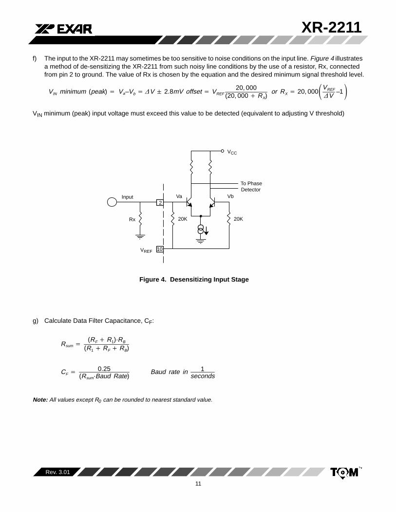
f) The input to the XR-2211 may sometimes be too sensitive to noise conditions on the input line. Figure 4 illustrates a method of de-sensitizing the XR-2211 from such noisy line conditions by the use of a resistor, Rx, connected from pin 2 to ground. The value of Rx is chosen by the equation and the desired minimum signal threshold level.
VIN minimum (peak) Va–Vb V 2.8mV offset VREF20, 000
(20, 000 RX)or RX 20, 000
VREF
V–1
VIN minimum (peak) input voltage must exceed this value to be detected (equivalent to adjusting V threshold)
ÎÎ
ÎÎÎÎ
VCC
Rx
Input2
20K
Va
20K
To PhaseDetector
Vb
VREF 10
Figure 4. Desensitizing Input Stage
g) Calculate Data Filter Capacitance, CF:
Rsum (RF R1)·RB
(R1 RF RB)
CF 0.25
(Rsum·Baud Rate)Baud rate in 1
seconds
Note: All values except R0 can be rounded to nearest standard value.

XR-2211
12
Rev. 3.01
4 6 8 10 12 14 16 18 20 22 24
1
2
3
4
55
2
43
1
12345
Curve R05K
10K30K
100K300K
V+ (Volts)
fO = 1kHzRF = 10R0
Nor
mal
ized
Fre
quen
cy D
rift (
% o
f f
)
R (
K
)
= 1 kHz
R0=5KΩ
Figure 5. Typical Supply Current vs. V+ (Logic Outputs Open Circuited)
Figure 6. VCO Frequency vs. Timing Resistor
Figure 7. VCO Frequency vs. Timing Capacitor Figure 8. Typical f O vs. Power SupplyCharacteristics
Figure 9. Typical Center Frequency Drift vs. Temperature
20
15
10
5
0
R0=10KΩ
R0>100K
4 6 8 10 12 14 16 18 20 22 24
ÎÎÎÎÎÎÎÎÎÎÎÎÎÎÎÎÎÎÎÎÎÎÎÎÎÎÎÎÎÎÎÎÎÎÎÎÎÎÎÎÎÎÎÎÎÎÎÎÎÎÎÎÎÎÎÎÎÎÎÎÎÎÎÎÎÎÎÎÎÎÎÎÎÎÎÎÎÎÎÎÎÎÎÎÎÎÎÎÎÎÎÎÎÎÎÎÎÎÎÎÎÎÎÎÎÎÎÎÎÎÎÎÎÎÎÎÎÎÎÎÎ
1.0
0.1
0.01100 1000 10000
fO(HZ)
+1.0
+0.5
0
-0.5
-1.0-50 -25 0 25 50 75 100 125
Temperature ( °C)
R0=1MΩ
R0=500K
R0=50K
R0=10K1MΩ
500K
50K
10K
V+ = 12VR1 = 10 R0fO
Supply Voltage, V + (Volts)
R0=20K
ÎÎÎÎÎÎÎÎÎÎÎÎÎÎÎÎÎÎÎÎÎÎÎÎÎÎÎÎÎÎÎÎÎÎÎÎÎÎÎÎÎÎÎÎÎÎÎÎÎÎÎÎÎÎÎÎÎÎÎÎÎÎÎÎÎÎÎÎÎÎÎÎÎÎÎÎÎÎÎÎÎÎÎÎÎÎÎÎÎÎÎÎÎÎÎÎÎÎÎÎÎÎÎÎÎÎÎÎÎÎÎÎÎÎÎÎÎÎÎÎÎÎÎÎÎÎÎÎÎÎÎÎ
1,000
100
100 1000 10000
fO(Hz)
1.02
1.01
1.00
0.99
0.98
0.97
R0=5K
C0=0.001F
C0=0.0033F
C0=0.01F
C0=0.0331F
C0=0.1F
C0=0.33F
R0=160K
R0=40K
R0=80K
R0=10K
0
Nor
mal
ized
Fre
quen
cy
O
Sup
ply
vs. C
urre
nt (
mA
)
C (
F
)0

XR-2211
13
Rev. 3.01
Design Example:
1200 Baud FSK demodulator with mark and space frequencies of 1200/2200.
Step 1: Calculate fO: from design instructions
(a) fO 1200·2200 =1624
Step 2: Calculate R0 : R0 =10K with a potentiometer of 10K. (See design instructions (b))
(b) RT 10102 15K
Step 3: Calculate C0 from design instructions
(c) CO 1
15000·1624 39nF
Step 4: Calculate R1 : from design instructions
(d) R1 20000·1624·2(2200–1200)
51, 000
Step 5: Calculate C1 : from design instructions
(e) C1 1250·39nF51000·0.52 3.9nF
Step 6: Calculate RF : RF should be at least five times R1, RF = 51,000⋅5 = 255 K
Step 7: Calculate RB : RB should be at least five times RF, RB = 255,000⋅5 = 1.2 M
Step 8: Calculate RSUM :
RSUM (RF R1)·RB
(RF R1 RB) 240K
Step 9: Calculate CF :
CF 0.25
RSUM·Baud Rate 1nF
Note: All values except R0 can be rounded to nearest standard value.
XR-2211
14
Rev. 3.01
VCC
RL5.1K5%
RB
1.8m 5%LoopPhaseDetect
11
C12.7nF5% R1
35.2K1%
8
FSKComp.
RF 178K
5% CF1nF 10%
7
DataOutput
InternalReference0.1µF
10
VCO
14 13
12
Rx20K
R020K1%
CO27nF 5%
2
0.1µF
InputSignal
LockDetectComp.
VCO
TuneFine
6LDOQ
5LDOQN
QuadPhaseDetect
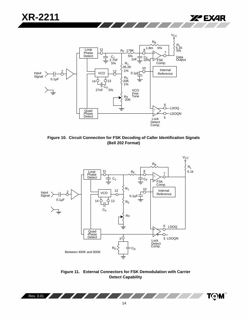
Figure 10. Circuit Connection for FSK Decoding of Caller Identification Signals(Bell 202 Format)
VCC
RL
5.1k
RB
LoopPhaseDetect C1
11
R1
RF
CF
8
FSKComp.
7
InternalReference
0.1µF
10VCO
14 13
12
R0
C0
Rx
2
0.1µF
InputSignal
LockDetectComp.
6 LDOQ
5 LDOQN3
CDRDBetween 400K and 600K
QuadPhaseDetect
Figure 11. External Connectors for FSK Demodulation with CarrierDetect Capability
+
+

XR-2211
15
Rev. 3.01
LoopPhaseDetect
11
C1220pF5% R1
200K1%
8
FSKComp.
VCC
7
InternalReference0.1µF
10
VCO
14 13
12
R020K1%C0
50nF 5%
Rx5K
2
0.1µF
InputTone
LockDetectComp.
TuneFine
6 LDOQ
RL25.1K
RL35.1K
Logic Output
5 LDOQN3
CD80nF
RD470K
QuadPhaseDetect
Figure 12. Circuit Connection for Tone Detection
VCC
VCO
+
+
FSK Decoding with Carrier Detect
The lock detect section of XR-2211 can be used as acarrier detect option for FSK decoding. Therecommended circuit connection for this application isshown in Figure 11. The open collector lock detect output,pin 6, is shorted to data output (pin 7). Thus, data outputwill be disabled at “low” state, until there is a carrier withinthe detection band of the PLL and the pin 6 output goes“high” to enable the data output.Note: Data Output is “Low” When No Carrier is Present.
The minimum value of the lock detect filter capacitanceCD is inversely proportional to the capture range, +fc.This is the range of incoming frequencies over which theloop can acquire lock and is always less than the trackingrange. It is further limited by C1. For most applications, fc> f/2. For RD = 470K, the approximate minimum valueof CD can be determined by:
CD16f
C in F and f in Hz.
C in F and f in Hz.
With values of CD that are too small, chatter can beobserved on the lock detect output as an incoming signal
frequency approaches the capture bandwidth.Excessively large values of CD will slow the response timeof the lock detect output. For Caller I.D. applicationschoose CD = 0.1F.
Tone Detection
Figure 12 shows the generalized circuit connection fortone detection. The logic outputs, LDOQN and LDOQ atpins 5 and 6 are normally at “high” and “low” logic states,respectively. When a tone is present within the detectionband of the PLL, the logic state at these outputs becomereversed for the duration of the input tone. Each logicoutput can sink 5mA of load current.
Both outputs at pins 5 and 6 are open collector typestages, and require external pull-up resistors RL2 andRL3, as shown in Figure 12.
With reference to Figure 3 and Figure 12, the functions ofthe external circuit components can be explained asfollows: R0 and C0 set VCO center frequency; R1 sets thedetection bandwidth; C1 sets the low pass-loop filter timeconstant and the loop damping factor.

XR-2211
16
Rev. 3.01
Design Instructions:
The circuit of Figure 12 can be optimized for any tone detection application by the choice of the 5 key circuit components:R0, R1, C0, C1 and CD. For a given input, the tone frequency, fS, these parameters are calculated as follows:
(All resistance in ’s, all frequency in Hz and all capacitance in farads, unless otherwise specified)
a) Choose value of timing resistor R0 to be in the range of 10K to 50K. This choice is dictated by the max./min. current that the internal voltage reference can deliver. The recommended value is R0 = 20K. The final value of R0 is normally fine-tuned with the series potentiometer, RX.
b) Calculate value of C0 from design equation (1) or from Figure 7 fS = fO:
CO1
R0·fs
c) Calculate R1 to set the bandwidth +f (See design equation 5):
R1R0·f0·2f
Note: The total detection bandwidth covers the frequency range of fO +f
d) Calculate value of C1 for a given loop damping factor:
Normally, = 0.5 is recommended.
C11250·C0
R1·2
Increasing C1 improves the out-of-band signal rejection, but increases the PLL capture time.
e) Calculate value of the filter capacitor CD . To avoid chatter at the logic output, with RD = 470K, CD must be:
CD16f
C in F
Increasing CD slows down the logic output response time.
Design Examples:
Tone detector with a detection band of + 100Hz:
a) Choose value of timing resistor R0 to be in the range of 10K to 50K. This choice is dictated by the max./min. current that the internal voltage reference can deliver. The recommended value is R0 = 20 K. The final value of R0 is normally fine-tuned with the series potentiometer, RX.
b) Calculate value of C0 from design equation (1) or from Figure 6 fS = fO:
C01
R0·fS
120, 000·1, 000
50nF
XR-2211
17
Rev. 3.01
c) Calculate R1 to set the bandwidth +f (See design equation 5):
R1R0·fO·2f
20, 000·1, 000·2100
400K
Note: The total detection bandwidth covers the frequency range of fO +f
d) Calculate value of C0 for a given loop damping factor:
Normally, = 0.5 is recommended.
C11250·C0
R1·2
1250·50·10–9
400, 000·0.52 6.25pF
Increasing C1 improves the out-of-band signal rejection, but increases the PLL capture time.
e) Calculate value of the filter capacitor CD . To avoid chatter at the logic output, with RD = 470K, CD must be:
CD16f
16200 80nF
Increasing CD slows down the logic output response time.
f) Fine tune center frequency with 5K potentiometer, RX.
0.1µFRF
100K
VCC
LoopPhaseDetect C1
11
R1
8
FSKComp.
7 3
21
4
11 LM324
CF
OutputDemodulated
InternalReference
6LDOQ
0.1µF
10
LockDetectComp.
VCO
14 13
12
R0
C0
2
0.1µFInputFM
QuadPhaseDetect 5
LDOQN
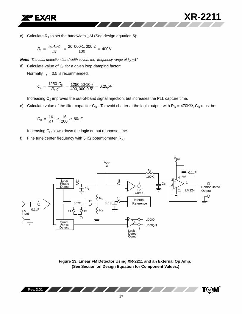
Figure 13. Linear FM Detector Using XR-2211 and an External Op Amp. (See Section on Design Equation for Component Values.)
VCC
+
+
+
XR-2211
18
Rev. 3.01
Linear FM Detection
XR-2211 can be used as a linear FM detector for a widerange of analog communications and telemetryapplications. The recommended circuit connection forthis application is shown in Figure 13. The demodulatedoutput is taken from the loop phase detector output (pin11), through a post-detection filter made up of RF and CF,and an external buffer amplifier. This buffer amplifier isnecessary because of the high impedance output at pin11. Normally, a non-inverting unity gain op amp can beused as a buffer amplifier, as shown in Figure 13.
The FM detector gain, i.e., the output voltage change perunit of FM deviation can be given as:
VOUTR1·VREF
100·R0
where VR is the internal reference voltage (VREF = VCC /2- 650mV). For the choice of external components R1, R0,CD, C1 and CF, see the section on design equations.
Capacitor
6
Input
5
7
Resistor
V+
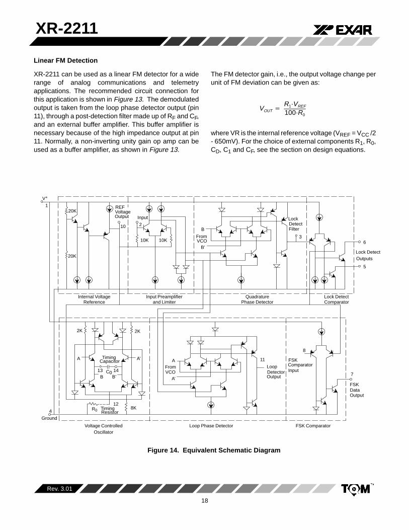
Figure 14. Equivalent Schematic Diagram
20K
20K
Internal VoltageReference
Input Preamplifierand Limiter
10K 10K
QuadraturePhase Detector
LockDetectFilter
Lock DetectOutputs
Lock DetectComparator
FSKDataOutput
FSKComparatorInput
LoopDetectorOutput
AFromVCO
2K
A’
Loop Phase Detector
8K12
R0
Timing
13B B’
C0 14
Voltage ControlledOscillator
REFVoltageOutput
10 2B
FromVCO
B’
3
2K
A
1
4
Ground
FSK Comparator
8
11
A’
Timing
XR-2211
19
Rev. 3.01
A 0.100 0.200 2.54 5.08
A1 0.015 0.060 0.38 1.52
B 0.014 0.026 0.36 0.66
B1 0.045 0.065 1.14 1.65
c 0.008 0.018 0.20 0.46
D 0.685 0.785 17.40 19.94
E1 0.250 0.310 6.35 7.87
E 0.300 BSC 7.62 BSC
e 0.100 BSC 2.54 BSC
L 0.125 0.200 3.18 5.08
α 0° 15° 0° 15°
L
D
B
e
B1
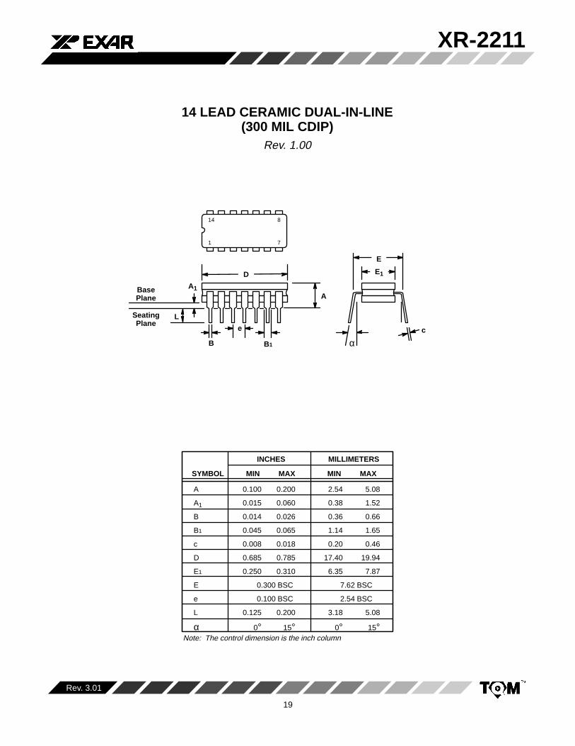
14 LEAD CERAMIC DUAL-IN-LINE(300 MIL CDIP)
Rev. 1.00
SYMBOL MIN MAX MIN MAX
INCHES MILLIMETERS
A1
αc
SeatingPlane
BasePlane A
14
1 7
8
E1
E
Note: The control dimension is the inch column

XR-2211
20
Rev. 3.01
14 LEAD PLASTIC DUAL-IN-LINE(300 MIL PDIP)
Rev. 1.00
14
1
8
7
D
e B1
A1
E1
E
AL
B
SeatingPlane
SYMBOL MIN MAX MIN MAX
INCHES
A 0.145 0.210 3.68 5.33
A1 0.015 0.070 0.38 1.78
A2 0.115 0.195 2.92 4.95
B 0.014 0.024 0.36 0.56
B1 0.030 0.070 0.76 1.78
C 0.008 0.014 0.20 0.38
D 0.725 0.795 18.42 20.19
E 0.300 0.325 7.62 8.26
E1 0.240 0.280 6.10 7.11
e 0.100 BSC 2.54 BSC
eA 0.300 BSC 7.62 BSC
eB 0.310 0.430 7.87 10.92
L 0.115 0.160 2.92 4.06
α 0° 15° 0° 15°
MILLIMETERS
α
A2
C
Note: The control dimension is the inch column
eB
eA
XR-2211
21
Rev. 3.01
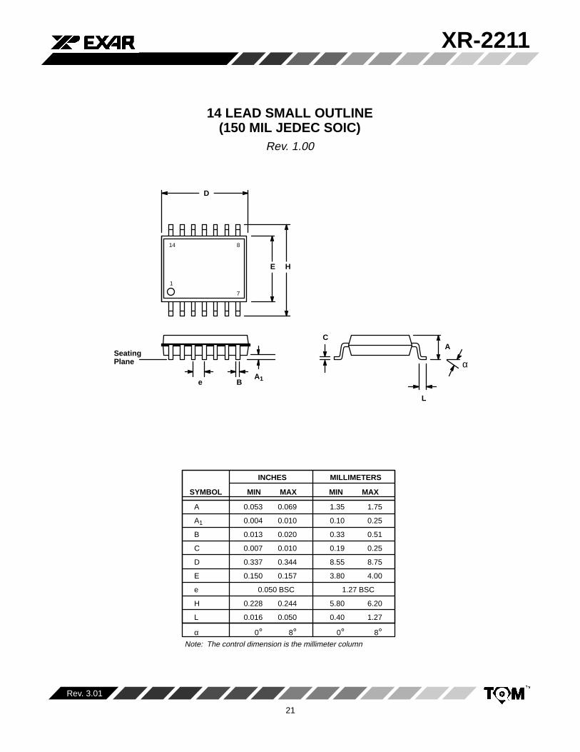
SYMBOL MIN MAX MIN MAX
A 0.053 0.069 1.35 1.75
A1 0.004 0.010 0.10 0.25
B 0.013 0.020 0.33 0.51
C 0.007 0.010 0.19 0.25
D 0.337 0.344 8.55 8.75
E 0.150 0.157 3.80 4.00
e 0.050 BSC 1.27 BSC
H 0.228 0.244 5.80 6.20
L 0.016 0.050 0.40 1.27
α 0° 8° 0° 8°
INCHES MILLIMETERS
14 LEAD SMALL OUTLINE(150 MIL JEDEC SOIC)
Rev. 1.00
e
14 8
7
D
E H
B
A
L
C
A1
SeatingPlane α
Note: The control dimension is the millimeter column
1
XR-2211
22
Rev. 3.01
Notes

XR-2211
23
Rev. 3.01
Notes
XR-2211
24
Rev. 3.01
NOTICE
EXAR Corporation reserves the right to make changes to the products contained in this publication in order to im-prove design, performance or reliability. EXAR Corporation assumes no responsibility for the use of any circuits de-scribed herein, conveys no license under any patent or other right, and makes no representation that the circuits arefree of patent infringement. Charts and schedules contained here in are only for illustration purposes and may varydepending upon a user’s specific application. While the information in this publication has been carefully checked;no responsibility, however, is assumed for inaccuracies.
EXAR Corporation does not recommend the use of any of its products in life support applications where the failure ormalfunction of the product can reasonably be expected to cause failure of the life support system or to significantlyaffect its safety or effectiveness. Products are not authorized for use in such applications unless EXAR Corporationreceives, in writing, assurances to its satisfaction that: (a) the risk of injury or damage has been minimized; (b) theuser assumes all such risks; (c) potential liability of EXAR Corporation is adequately protected under the circum-stances.
Copyright 1995 EXAR CorporationDatasheet June 1997Reproduction, in part or whole, without the prior written consent of EXAR Corporation is prohibited.


