dp3500-4500 sm.pdf
DESCRIPTION
service toshiba DP 3500TRANSCRIPT

Copyright TOSHIBA CORPORATION 2001ALL RIGHTS RESERVED
Click the Navigation Pane button to open the overview area anddisplay bookmarks and thumbnails palettes.
Click the Bookmarks to open the Contents and display Bookmarkscreated for the document. Click a bookmark's name to go to the Page marked by that bookmark.
Click the Thumbnails to open the overview area and displaythumbnail images of each document page. Click a thumbnail to go to the Page marked by that thumbnail.
SERVICE MANUAL DIGITAL PLAIN PAPER COPIER DP4500/3500

GENERAL PRECAUTIONS REGARDING THE INSTALLATIONAND SERVICE FOR THE COPIER DP4500/3500
The installation and service should be done by a qualified service technician.
1. Transportation/Installation
• When transporting/installing the copier, employ two persons and be sure to use the positions as
indicated below.
The copier is quite heavy and weighs approximately 73kg (161lb), therefore pay full attention when
handling it.
• Be sure to use a dedicated outlet with AC 115V or 120V/15A (220V, 230V, 240V/10A) or more for
its power source.
• The copier must be grounded for safety.
Never ground it to a gas pipe or a water pipe.
• Select a suitable place for installation.
Avoid excessive heat, high humidity, dust, vibration and direct sunlight.
• Also provide proper ventilation as the copier emits a slight amount of ozone.
• To insure adequate working space for the copying operation, keep a minimum clearance of
80 cm (32”) on the left, 80 cm (32”) on the right and 10 cm (4”) in the rear.
• The socket-outlet shall be installed near the copier and shall be easily accessible.
2. Service of Machines
• Basically, be sure to turn the main switch off and unplug the power cord during service.
• Be sure not to touch high-temperature sections such as the exposure lamp, the fuser unit, the
damp heater and their periphery.
• Be sure not to touch high-voltage sections such as the chargers, high-voltage transformer, IH
control circuit, exposure lamp control inverter, inverter for the LCD backlight and power supply
unit. Especially, the board of these components should not be touched since the electirc charge
may remain in the condensers, etc. on them even after the power is turned OFF.
• Be sure not to touch rotating/operating sections such as gears, belts, pulleys, fan, etc.
• Be careful when removing the covers since there might be the parts with very sharp edges under-
neath.
• When servicing the machines with the main switch turned on, be sure not to touch live sections
and rotating/operating sections. Avoid exposure to laser radiation.
• Use suitable measuring instruments and tools.
• Avoid exposure to laser radiation during servicing.
− Avoid direct exposure to the beam.
− Do not insert tools, parts, etc. that are reflective into the path of the laser beam.
− Remove all watches, rings, bracelets, etc. that are reflective.

3. Main Service Parts for Safety
• The breaker, door switch, fuse, thermostat, thermofuse, thermistor, etc. are particularly important
for safety. Be sure to handle/install them properly.
4. Cautionary Labels
• During servicing, be sure to check the rating plate and the cautionary labels such as “Unplug the
power cord during service”, “Hot area”, “Laser warning label” etc. to see if there is any dirt on their
surface and whether they are properly stuck to the copier.
5. Disposition of Consumable Parts/Packing Materials
• Regarding the recovery and disposal of the copier, supplies, consumable parts and packing mate-
rials, it is recommended to follow the relevant local regulations or rules.
6. When parts are disassembled, reassembly is basically the reverse of disassembly unless
otherwise noted in this manual or other related documents. Be careful not to reassemble
small parts such as screws, washers, pins, E-rings, star washers in the wrong places.
7. Basically, the machine should not be operated with any parts removed or disassembled.
8. Precautions Against Static Electricity
• The PC board must be stored in an anti-electrostatic bag and handled carefully using a wristband,
because the ICs on it may become damaged due to static electricity.
Caution: Before using the wristband, pull out the power cord plug of the copier and make
sure that there are no uninsulated charged objects in the vicinity.
Caution : Dispose of used batteries and RAM-ICs including lithium batteries
according to the manufacturer’s instructions.
Attention : Se débarrasser de batteries et RAM-ICs usés y compris les batteries en
lithium selon les instructions du fabricant.
Vorsicht : Entsorgung des gebrauchten Batterien und RAM-ICs (inklusive
der Lithium-Batterie) nach Angaben des Herstellers.

December 2000 © TOSHIBA TEC 1 - 1 DP4500/3500 SPECIFICATIONS
1. SPECIFICATIONS / ACCESSORIES / OPTIONS / SUPPLIES
1.1 Specifications
Values in [ ] are for DP3500 only when the specifications are different for the DP4500 and the DP3500.
• Copy process Indirect electrophotographic process (dry)
• Type Desktop type (console type when paper feed pedestal (PFP) and large capacity
feeder (LCF) are installed)
• Original table Fixed type (the left rear corner used as guide to place originals)
• Acceptable originals Sheet, book and 3-dimensional object. The automatic document feeder (option)
only accepts paper (64~80 g/m2/17~22 lb.) excluding carbon paper, pasted sheet
and stapled sheet.
Maximum size : A3/LD
• Copy speed (Copies/min.)
* “–” means “Cannot be used”.
* The copy speeds in the above table are available when the originals are manually placed for single-side,
multiple copying.
* When the automatic document feeder is used, the copy speed of 45 [35] sheets per minute is only
available under the following conditions:
• Original/Mode: Single-side originals of A4/LT size. APS and automatic density are
not selected.
• Number of sheets: 45 [35] or more.
• Reproduction ratio: 100%
Paper supply Paper size
A4, LT, B5
A4-R, B5-R,
A5-R, LT-R, ST-R
B4, LG
A3, LD
Cassette
45 [35]
28 [25]
24 [21]
21 [18]
Size specified
45 [35]
28 [25]
24 [21]
21 [18]
Size not specified
21 [18]
21 [18]
21 [18]
21 [18]
PFP
45 [35]
28 [25]
24 [21]
21 [18]
Bypass feeding LCF
(only A4/LT)
45 [35]
–
–
–

DP4500/3500 SPECIFICATIONS 1 - 2 December 2000 © TOSHIBA TEC
* System copy speed (DP4500)
Copy mode Copies/min.
Single-sided originals 1 set 34
x 3 sets 39
Single-sided copies 5 sets 41
Single-sided originals 1 set 19
x 3 sets 28
Two-sided copies 5 sets 30
Two-sided originals 1 set 17
x 3 sets 25
Two-sided copies 5 sets 28
Two-sided originals 1 set 19
x 3 sets 30
Single-sided copies 5 sets 35
* The copy speeds in the table include the time for
the first copy. They are available when the copy
modes in the left-hand table are selected and 10
A4-sized originals are set in the automatic docu-
ment feeder.
• Copy paper
Cassette Duplex copy PFP LCF Bypass copy Remarks
Size A3~A5R A4, LT A3~A5-R, LD~ST-RLD~ST-R (Non-standard or user-
specified sizes can be set.)
Weight 64~80g/m2, 17~22 lb. 64~80 g/m2,17~22lb(Continuous feeding)
50~209 g/m2, 14~55 lb(Single paper feeding)
Special – Tracing paper, labels, Special types of paperpaper OHP film (thickness: 80µm must be recommended
or thicker) by Toshiba
• First copy time .................. 3.9 seconds or faster (A4/LT, upper cassette, 100%, original placed manu-
ally)
• Warming-up time ................ Approx. 30 seconds (standalone, temperature: 20°C)
• Multiple copying................. Up to 999 copies; set number entered with digital keys
• Reproduction ratio .............. Actual ratio: 100±0.5%
Zooming: 25~400% in increments of 1% (25~200% when
using the RADF)
• Resolution/Gradation ......... Read: 600 dpi
......... Write: Equivalent to 2400 dpi x 600 dpi
(primary scanning only : 4 division smoothing)
• Eliminated image width ...... Leading/trailing edges: 2.0±1.0 mm, Side edges: 2.0±2.0 mm

December 2000 © TOSHIBA TEC 1 - 3 DP4500/3500 SPECIFICATIONS
• Paper feeding ..................... Automatic feeding: Copier cassettes–2 cassettes (paper stack height
60.5 mm, equivalent to 550 sheets; 64 to 80 g/m2
(17 to 22 lb.))
PFP–Optional (One cassette or two: paper stack
height 60.5 mm: equivalent to 550 sheets; 64 to 80 g/
m2 (17 to 22 lb.))
LCF–Optional (Paper stack height 137.5 mm x 2:
equivalent to 2500 sheets; 64 to 80 g/m2, 17 to 22 lb.)
Bypass feeding: (Paper stack height 11 mm : equivalent to 100 sheets;
64 to 80 g/m2, 17 to 22 lb.)
• Capacity for originals in the automatic document feeder (Optional)
................. A3~A5-R, LD~ST-R : 100 sheets
• Automatic duplexing unit ... Stackless, Switchback type
• Toner supply ...................... Automatic toner density detection/supply
Toner cartridge replacing method
• Density control .................. Automatic density mode and manual density mode selectable in 11 steps
• Weight ............................... Approx. 73 kg, 161 lb
• Power requirements ........... AC 115V/15A, AC 220 – 240V/10A
• Power consumption ........... 2.0 kW or less (115V series, 200V series)
* Electric power is supplied to the automatic document feeder, finisher, PFP and LCF through the
copier.
• Total counter ...................... Electronic counter

DP4500/3500 SPECIFICATIONS 1 - 4 December 2000 © TOSHIBA TEC
• Dimensions of copier ......... See the figure below (W660 x D673 x H739 mm)
73
9
660
673

December 2000 © TOSHIBA TEC 1 - 5 DP4500/3500 SPECIFICATIONS
1.2 Accessories
Unpacking/setup instructions 1 pc.
Operator’s Manual 1 pc. (not available for MJD)
PM sticker 1 pc. (for MJD)
Setup report 1 set. (for NAD and MJD)
Customer satisfaction card 1 pc. (for MJD)
Developer material 1 pc. (not available NAD and MJD)
Toner cartridge 1 pc. (not available NAD and MJD)
Operator’s Manual pocket 1 pc.
Power cable 1 pc.
Preventive maintenance check list 1 pc. (for MJD)
Toner bag symbol sticker 1 pc. (for MJD)
Warranty sheet 1 pc. (for NAD)
* Machine version
NAD: North America
MJD: Europe
AUD: Australia
ASD: Asia

DP4500/3500 SPECIFICATIONS 1 - 6 December 2000 © TOSHIBA TEC
1.3 Options
Platen cover KA-1600PC
Automatic document feeder (RADF) MR-3012
Paper feed pedestal (PFP) KD-1009
Cassette module MY-1017
Large capacity feeder (LCF) KD-1010
Finisher MJ-1011 (for DP3500), MJ-1012, MJ-1013
Hole punch unit MJ-6001
Staple cartridge STAPLE-1600, STAPLE-600, STAPLE-700
Key copy counter, key copy counter socket MU-8, MU-10
Work table KK-3500
Damp heater kit MF-3500U, MF-3500E
Desk(H) MH-1600H
Desk(L) MH-1600L
System controller GL-1010, GL-1010E
Option for system controller GC-1090 (Extended memory)
GB-1040 (PC-Fax)
GB-1060 (Scan/E-mail Print)
SC-2-TKRING-NIC (TokenRingNIC)
GF-1100 (I/F board for protocol converter)
Printer controller GA-1040
Option for printer controller GC-1080 (Extended memory)
GB-1070 (CWS)
GB-1080 (FreeForm)
GB-1090 (DocBuilderPro)
GE-1020 (PS3 without HDD)
GE-1030 (PS3 with HDD)
Fax unit GD-1080NA/EU/TW/AU
Option for fax unit GD-1090NA/EU (2nd line unit)
1.4 Supplies
Toner PS-ZT3500, PS-ZT3500E, PS-ZT3500D
Toner bag PS-TB3500, PS-TB3500E

December 2000 © TOSHIBA TEC 1 - 7 DP4500/3500 SPECIFICATIONS
1.5 System List
Sta
ple
cart
ridge
STA
PLE
-160
0
Sta
ple
cart
ridge
STA
PLE
-700
Sta
ple
cart
ridge
STA
PLE
-600
Hol
e pu
nch
unit
MJ-
6001
Pap
er fe
ed p
edes
tal (
PF
P)
KD
-100
9
Larg
e ca
paci
ty f
eede
r(L
CF
)K
D-1
01
0
Fin
ishe
r re
lay
unit
Wor
k ta
ble
KK
-350
0
Key
cop
y co
unte
rso
cket
MU
-10
Key
cop
y co
unte
rM
U-8
Aut
omat
ic d
ocum
ent
feed
er (
RA
DF
)M
R-3
01
2
Pla
ten
cove
rK
A-1
600P
C
Fin
ishe
rM
J-10
11
Cas
sette
mod
ule
MY-
1017
Fin
ishe
rM
J-10
13
Fin
ishe
rM
J-10
12

DP4500/3500 SPECIFICATIONS 1 - 8 December 2000 © TOSHIBA TEC

December 2000 © TOSHIBA TEC 2 - 1 DP4500/3500 OUTLINE OF THE MACHINE
2. OUTLINE OF THE MACHINE
2.1 Sectional View
2. OUTLINE OF THE MACHINE
2.1 Sectional View
9 1081
342756
5557
58
11
5652
504849
5154
5347
40 4133
3936 38
37 32
35
34
434245
44
59
62
60
2963
3061
2627
25 24
2328
2218
19
20
21
17
1312 14,15,16
31
46
65
66

DP4500/3500 OUTLINE OF THE MACHINE 2 - 2 December 2000 © TOSHIBA TEC
1 Original glass
2 Exposure lamp
3 Inverter
4 Mirror-1
5 Mirror-2
6 Mirror-3
7 Carriage home position sensor
8 Lens
9 CCD drive PC board
10 Scanner control PC board
11 Laser optical unit
12 Cassette
13 Cassette tray
14 Paper-empty sensor
15 Paper-stock sensor
16 Tray-up sensor
17 Cassette pickup roller
18 Cassette feed roller
19 Cassette separation roller
20 Transport roller
21 Lower feed sensor
22 Upper feed sensor
23 Bypass tray
24 Bypass guide
25 Bypass pickup roller
26 Bypass paper sensor
27 Bypass feed roller
28 Bypass separation pad
29 Registration sensor
30 Registration roller
31 Drum
32 Separation finger for drum
33 Main charger
34 Transfer guide
35 Transfer/separation charger
36 Cleaning blade
37 Recovery blade
38 Toner recovery auger
39 Discharge lamp
40 Toner cartridge
41 Toner motor
42 Developer sleeve (magnetic roller)
43 Doctor blade
44 Mixer-1
45 Mixer-2
46 Auto-toner sensor
47 Fuser unit entrance guide
48 Fuser roller
49 IH coil
50 Fuser roller thermostat
51 Fuser roller thermistor
52 Separation finger for fuser roller
53 Pressure roller
54 Cleaning roller
55 Separation finger for pressure roller
56 Exit finger
57 Fuser unit cover
58 Exit roller
59 ADU upper transport roller
60 ADU middle transport roller
61 ADU lower transport roller
62 ADU entrance sensor
63 ADU exit sensor
64 Paper receiving tray
65 Drum thermistor
66 Humidity sensor

December 2000 © TOSHIBA TEC 2 - 3 DP4500/3500 OUTLINE OF THE MACHINE
2.2 Location of Electrical Parts[A] Arrang ement of Various Units
ADU
Scanner unit
Main unit
Rear side
Laser unit
System unit

DP4500/3500 OUTLINE OF THE MACHINE 2 - 4 December 2000 © TOSHIBA TEC
M1
[B] Scanner unit
(B-1) Motor
Rear side
(B-2) Sensors and switches
Rear side
S27
S10
S5S6
S4S3S2
S1
*A4 series : S1 to 5 are installed. LT series : S1 to 3 and S6 are installed.

December 2000 © TOSHIBA TEC 2 - 5 DP4500/3500 OUTLINE OF THE MACHINE
(B-3) PC boards
(B-4) Others
CCD
SDV
SLGRear side
Rear side
DHM
EXPINV
DHL

DP4500/3500 OUTLINE OF THE MACHINE 2 - 6 December 2000 © TOSHIBA TEC
LGC
HDD
FAX
NCU-US
BRG
CPU
CD-ROM
FAN-SCPWR-SC
HDD-SC
MDM
SYS
PRT
NIC
HDD-PRT
[C] System unit
Rear side
Fax
Printer
Systemcontroller

December 2000 © TOSHIBA TEC 2 - 7 DP4500/3500 OUTLINE OF THE MACHINE
[D] Laser unit
Rear side
LDR
SNS
M2
M3
POL
[E] ADU
S24
ADU
CLT1
S22
S23
M4
Rear side

DP4500/3500 OUTLINE OF THE MACHINE 2 - 8 December 2000 © TOSHIBA TEC
[F] Main unit
(F-1) Motors and fans
(F-2) PC boards and AC parts
M10
M13
M11
M8
M5 M12
M15
M6 M7
M14
IHCOIL
S8
S7
ACC
THERM1
IH
DHC
FUSE
DHD
Rear side
Rear side
December 2000 © TOSHIBA TEC 2 - 9 DP4500/3500 OUTLINE OF THE MACHINE
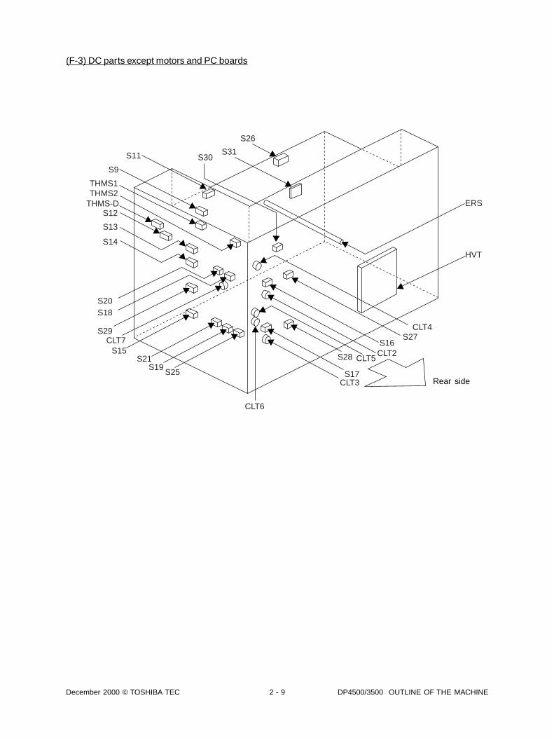
(F-3) DC parts except motors and PC boards
Rear side
S9
S26
S30
HVT
ERS
S27S16
CLT4
S31
S28
S17CLT3
CLT6
S25S19
S21S15
CLT7S29
S18
CLT2CLT5
S20
S14
S13
S12
S11
THMS-DTHMS2THMS1

DP4500/3500 OUTLINE OF THE MACHINE 2 - 10 December 2000 © TOSHIBA TEC
2.3 Symbols and Functions of Various Components
<P-I> indicates page and item number in the parts list.(1) Motors
Symbol Name Function Remarks
M1 SCAN-MOT <P12-I9> Drives the carriages. (B-1)Scanner motor
FAN-SC FAN-534 Cools down the system controller unit. [C]System controller cooling fan [Optional]
M2 M/DC-POL-320 Drives the polygonal mirror. [D]Polygonal motor
M3 FAN-DC-320 <P7-I28> Cools down the laser optical unit. [D]Laser unit fan
M4 ADU-MTR <P32-I18> Drives the ADU. [E]ADU motor
M5 MAIN-MTR <P11-I26> Drives the drum, developer unit and fuser (F-1)Main motor unit.
M6 EXIT-MTR <P6-I11> Drives the exit roller. (F-1)Exit motor
M7 TNR-MTR <P27-I9> Supplies the toner. (F-1)Toner motor
M8 T-UP-MTR <P4-I22> Drives the cassette tray upward. (F-1)Tray-up motor
M10 SP-FAN <P10-I2> Assists the paper separation by suction. (F-1)Sub-separation fan
M11 EXIT-FAN <P10-I2> For exhaustion. (F-1)Exhaust fan
M12 IH-FAN <P8-I3> Cools down the IGBT for fuser control. (F-1)IH control board cooling fan
M13 MID-FAN <P8-I3> Cools down the drum and cleaner unit. (F-1)Middle cooling fan
M14 FUSER-FAN <P29-I13> Cools down the fuser unit. (F-1)Fuser unit cooling fan
M15 DEV-FAN <P6-I33> Cools down the developer unit. (F-1)Developer unit cooling fan

December 2000 © TOSHIBA TEC 2 - 11 DP4500/3500 OUTLINE OF THE MACHINE
Symbol Name Function Remarks
(2) Sensos and switches
S1-6 APS1-6 <P9-I17,18> Detects the size of originals. (B-2)Automatic original detection sensor
S10 HOME-SW <P9-I22> Detects the home position of the carriage. (B-2)Carriage home position switch
S27 PLTEN-SNR <P12-I15> Detects if the platen cover is opened/closed. (B-2)Platen sensor
S22 ADU-TRU-SNR <P32-I31> Detects paper in the paper entrance area [E]ADU entrance sensor of the ADU.
S23 ADU-TRL-SNR <P32-I31> Controls paper transport in the ADU. [E]ADU exit sensor
S24 ADU-SET-SW <P32-I43> Detects if the ADU is opened/closed. [E]ADU opening/closing switch
S7 MAIN-SW <P5-I10> Shuts off the AC power to the copier. (F-2)Main switch
S8 DOOR-SW <P5-I7> Interlock switch to shut off the AC power (F-2)Front door switch when the front cover is opened.
S9 EXIT-SNR <P30-I21> Detects paper in the paper exit area. (F-3)Exit sensor
S11 TNR-SW <P27-I23> Detects the toner cartridge. (F-3)Toner cartridge detection switch
S12 SNR-ATC <P25-I19> Detects the toner density. (F-3)Auto-toner sensor
S13 RGST-SNR <P18-I11> Detects if paper has reached the registration (F-3)Registration sensor roller.
S14 FED-U-SNR <P18-I11> Detects paper misfeeding. (F-3)Upper feed sensor
S15 FED-L-SNR <P18-I5> Detects paper misfeeding. (F-3)Lower feed sensor
S16 NEMP-U-SNR <P13-I27> Informs that the upper cassette is almost (F-3)Upper cassette paper-stock sensor empty.
S17 NEMP-L-SUR <P13-I27> Informs that the lower cassette is almost (F-3)Lower cassette paper-stock sensor empty.
S18 EMP-U-SNR <P13-I27> Detects presence/absence of paper in the (F-3)Upper cassette paper-empty sensor upper cassette.
S19 EMP-L-SNR <P13-I27> Detects presence/absence of paper in the (F-3)Lower cassette paper-empty sensor lower cassette.
S20 TOP-U-SNR <P13-I27> Detects if the upper cassette tray has been (F-3)Upper cassette tray-up sensor lifted to the upper limit.
S21 TOP-L-SNR <P13-I27> Detects if the lower cassette tray has been (F-3)Lower cassette tray-up sensor lifted to the upper limit.
S25 CST-COVER-SW <P5-I19> Detects if the the side door is opened/ (F-3)Side door switch closed.
S26 F-COV-SW <P5-I7> Detects if the front cover is opened/closed. (F-3)Front cover switch
S27 CST-U-SW <P4-I5> Detects if the upper cassette is installed. (F-3)Upper cassette detection switch
S28 CST-L-SW <P4-I5> Detects if the lower cassette is installed. (F-3)Lower cassette detection switch

DP4500/3500 OUTLINE OF THE MACHINE 2 - 12 December 2000 © TOSHIBA TEC
Symbol Name Function Remarks
Symbol Name Function Remarks
(3) Electromagnetic spring clutches
CLT1 ADU-CLT <P32-I16> Drives ADU. [E]ADU clutch
CLT2 FED-U-CLT <P13-I14> Drives the pickup roller for the upper (F-3)Upper cassette feed clutch cassette.
CLT3 FED-L-CLT <P13-I14> Drives the pickup roller for the lower (F-3)Lower cassette feed clutch cassette.
CLT4 RGST-CLT <P18-I31> Drives the registration roller. (F-3)Registration clutch
CLT5 TR-L-CLT <P14-I20> Transport paper from the registration area. (F-3)Transport clutch (low speed)
CLT6 TR-H-CLT <P14-I16> Transport paper up to the registration area. (F-3)Transport clutch (high speed)
CLT7 SFB-CLT <P16-I17> Drives the bypass pickup roller. (F-3)Bypass feed clutch
(4) Heaters and lamps
EXP LP-EXPO-50K-320 <P20-I2> Exposes the original with light. (B-4)Exposure lamp
DHM DNP-HTR <P9-I8> Prevents condensation in the scanning area (B-4)Damp heater (for mirrors).
DHL DNP-HTR <P9-I30> Prevents condensation in the scanning area (B-4)Damp heater (for lens).
DHD D-HTR-L <P26-I7> Keeps the drum and transfer/separation (F-2)Lower damp heater charger warm.
DHC D-HTR-CST <P4-I34> Prevents condensation in the cassettes. (F-2)Cassette damp heater
IHCOIL IH-COIL <P30-I23> Heats up the fuser roller. (F-2)IH coil
ERS LP-ERS <P24-I33> Removes the residual charge from the drum (F-3)Discharge lamp surface.
Symbol Name Function Remarks
S29 SFB-SNR <P17-I25> Detects presence/absence of paper in the (F-3)Bypass paper sensor bypass tray .
S30 T-FUL-SNR <P11-I28> Detects if the toner bag is full. (F-3)Toner bag full detection sensor
S31 HUMI-SNR <P7-I25> Detects humidity inside the copier. (F-3)Humidity sensor

December 2000 © TOSHIBA TEC 2 - 13 DP4500/3500 OUTLINE OF THE MACHINE
Symbol Name Function Remarks
Symbol Name Function Remarks
(5) PC boards
SLG PWA-F-SLG-320 <P9-I13> Controls the scanner section. (B-3)Scanner control PC board (SLG board)
CCD PWA-F-CCD-320 Controls pre-processing of the CCD image (B-3)CCD drive PC board (CCD board) data.
SDV PWA-F-SDV-320 <P12-I22> Controls the scanner motor. (B-3)Scanner motor drive PC board (SDV board)
SYS PWA-F-SYS-320 <P7-I18> General control of the copier and data [C]System PC board (SYS board) processing.
LGC PWA-F-LGC-320 <P7-I19> General control of the copier [C]Logic PC board (LGC board)
FAX PWA-F-FAX-527 <P1-I11> Controls the fax function. [C]Fax control board [Optional]
MDM PWA-F-MDM-528 <P2-I15> Controls dialing for the analog circuit (2nd [C]Telephone circuit control board circuit) [Optional]
NCU-US PWA-F-NCU-US <P1-I12> Controls dialing for the analog circuit (2nd [C]Telephone circuit control board circuit) [Optional]
PRT PWA-F-PRT-533 Controls the printer function. [C]Printer control board [Optional]
NIC NIC Connects the printer with the network. [C]Network board [Optional]
BRG PWA-F-BRG-534 Connects the system controller with the [C]Bridge board copier. (PCI to PCI bridge board) [Optional]
CPU PWA-F-SBC-534 Controls the system controller. [C] System controller CPU board [Optional]
LDR PWA-F-LDR-320 Drives the laser diode. [D]Laser drive PC board (LDR board)
POL M/DC-POL-320 Drives the polygonal motor. [D]Polygonal motor drive board
SNS PWA-F-SNS-320 Detects the laser beam position. [D]H-Sync detection PC board
ADU PWA-F-ADU-320 <P32-I30> Drives the ADU. [E]ADU board
IH PS-IH-320 <P31-I2> Controls the IH of the fuser unit. (F-2)IH control board
FUSE PWA-F-FUS <P6-I36> Prevents over-current being supplied to the (F-2)Fuse PC board damp heaters.
HVT PS-HVT-320 <P4-I29> Generates the voltage for the following: (F-3)High-voltage transformer • main charger wire
• main charger grid• developer bias• transfer charger wire• separation charger wire• transfer guide bias
(6) Transformer

DP4500/3500 OUTLINE OF THE MACHINE 2 - 14 December 2000 © TOSHIBA TEC
INV INV-EXP-50K-320 <P20-I3> Controls the exposure lamp. (B-4)Lamp inverter
HDD HDD <P7-I15> Stores the image data. [C]Hard disk
HDD OPTION-HDD-533 Extends the functions of the printer. [C]-PRT Hard disk (for printer) [Optional]
CD-ROM CD-ROM-534 A part of the system controller. Reads the [C]CD-ROM drive data. [Optional]
HDD HDD-534 Sub-memory for the system controller. [C]-SC Hard disk (for system controller) [Optional]
PWR PS-534 Power supply for the system controller [C]-SC Power supply for system controller [Optional]
ACC PS-ACC-320 <P6-I26> Provides the electrical power. (F-2)Switching power supply
THERM1 THERMO-HTR <P28-I9> Prevents the over-heating of the fuser unit. (F-2)Thermostat
THMS-D THMS-DRM <P25-I29> Detects the surface temperature of the (F-3)Drum thermistor drum.
THMS1 THMS-HTR <P28-I10> Detects the surface temperature of the (F-3)Fuser roller center thermistor center area of the fuser roller.
THMS2 THMS-S-HTR <P28-I10> Detects the surface temperature of the ends (F-3)Fuser roller side thermistor of the fuser roller.
Symbol Name Function Remarks
(7) Others

December 2000 © TOSHIBA TEC 2 - 15 DP4500/3500 OUTLINE OF THE MACHINE
2.4 System Block Diagram
Imag
e D
ata
Ser
ial-I
/F
PW
A-F
-SLG
-320
PW
A-F
-LG
C-3
20
SR
AM
256K
B
NV
RA
M8K
Bx8
S-C
PU
TM
P95
C06
316
bit
SR
AM
256K
B
Ser
ial-I
/F
16
Ser
ial-I
/F
16
Imag
e D
ata
M-C
PU
TM
P95
C06
3F16
bit
PF
P
AD
U
IPC
Fin
ishe
r
8
20M
ADR/DAT-Bus
5MH
z
8
ASM-F-PNL-320
LCD7 8 9
4 5 6
1 2 3
0 CLR/STP
AS
IC33
MH
z(Q
FP
176)
3.3V ISA-Bus
32
5MH
z
Sys
tem
cont
rolle
r
HD
D
20M
8.3M
FR
OM
16M
Bx2
3.3V ROM-Bus
16
TX
3927
CP
U32
bit-
RIS
CS
peed
:133
MH
z
SD
RA
M64
MB
x4
32/1
6
PW
A-F
-CC
D-3
20
20M
Hz
40M
Hz
40M
Hz
8
40M
Hz
20M
Am
p
A/D
PW
A-F
-LD
R-3
20
AS
ICLD
259
MH
z/4-
divi
ded
LVD
S
8bit
D/A
Lase
rB
eam
Sen
sor
DR
AM
32M
B
32
SD
RA
M64
Mbi
t
Tota
l:32M
B
20M
Hz
FAX
boa
rd3.
3V P
CI-
Bus
Imag
e D
ata
20M
Hz
CC
D
66M
66M
Hz
20M
5V ADR/DAT-Bus
AS
IC33
MH
z/66
MH
z(3
52B
GA
)
‚R
AS
IC40
MH
z(3
24B
GA
)
NV
RA
M8K
Bx8
RT
C
AS
IC40
MH
z(2
08Q
FP
)
IDE
I/F
SR
AM
4MB
8
BT
5V 5V
5V
3.3V
3.3V
5V
3.3V
5V
23.
3V
3.3V
59M
3.3V
SD
RA
M-B
US
Tota
l:32
MB
Tota
l: 4M
BF
RO
M4M
B
8
4
FR
OM
4MB
5V
3
.3V
80
5V
5V
Ser
ial-I
/F
LCA
301
AS
IC
8M
5V‚R
3.3V
AS
IC D
ebug
EW
S68
DR
AM
32M
BS
DR
AM
64M
B
SC
N_M
T
PW
A-F
-DLM
-320
PW
A-F
-DLS
-320
DR
IVE
R2
or 3
5Vto
rela
nt
5VI/F
5VI/F
5V
3.3
V
(skt
)
5V/3
.3V
LAN
Prin
ter
PW
A-F
-AD
U-3
20
PW
A-F
-SY
S-3
20
Sca
nner
Prin
ter
Sys
tem
EP
RO
M4M
Bx2
EP
RO
M16
MB
x2
PW
A-F
-DLM
-320
EP
RO
M4M
Bx2
RA
DF

DP4500/3500 OUTLINE OF THE MACHINE 2 - 16 December 2000 © TOSHIBA TEC
2.5 Installation and Removal ofCovers and PC board
2.5.1 Installation and removal of covers
[A] Front cover
(1) Open the front cover.
(2) Pull up the hinge pins on the left and the right,
then extract them.
(3) Remove the front cover.
[B] Front side right cover
(1) Pull out the upper cassette.
(2) Open the front cover, bypass unit and ADU.
(3) Remove 2 screws.
(4) Remove the front side right cover.
[C] Feed side front hinge cover
(1) Pull out the upper and lower cassettes.
(2) Remove 2 screws and take off the feed side
front hinge cover.
[D] Feed side rear hinge cover
(1) Remove 2 screws and take off the feed side
rear hinge cover.
Hinge pin Front cover
Front side right cover
ADU
Bypass unit
Feed side front hinge cover
Feed side rear hinge cover
December 2000 © TOSHIBA TEC 2 - 17 DP4500/3500 OUTLINE OF THE MACHINE
[E] Feed side upper cover
(1) Open the bypass unit, ADU, jam access cover
and fuser unit cover.
(2) Remove 2 screws.
(3) Slide the feed side upper cover to the left to
take it off.
[F] Feed side lower cover
(1) Remove the feed side rear hinge cover.
(2) Open the bypass feed unit and ADU.
(3) Remove 2 screws and take off the feed side
lower cover.
[G] Rear side upper cover
(1) Remove 4 screws and take off the rear side
upper cover.
[H] Rear side lower cover
(1) Remove 2 screws.
(2) Slide the rear side lower cover to the right to
take it off.
[I] Receiving tray
(1) Open the front cover.
(2) Remove 2 screws.
(3) Slide the receiving tray upwards to the left to
take it off.
Fuser unitcover
ADUJam accesscover
Feed sidelower cover
Rear sideupper cover
Rear sidelower cover
Receivingtray
Feed sideupper cover

DP4500/3500 OUTLINE OF THE MACHINE 2 - 18 December 2000 © TOSHIBA TEC
[J] Tray bac k co ver
(1) Remove the receiving tray.
(2) Take off the feed side upper cover.
(3) Remove 2 screws.
(4) Slide the tray back cover to the left and take it
off.
[K] Left cover
(1) Remove 3 screws and take off the left cover.
[L] Option cover
(1) Slide the cover in the direction of the arrow and
take it off.
[M] Exit side rear cover
(1) Take off the rear side upper/lower covers.
(2) Loosen the screws of the receiving tray and left
cover.
(3) Remove 4 screws and take off the exit side rear
cover.
Left cover
Option cover Receivingtray
Leftcover
Tray back cover
Rear sideuppercover
Rear sidelowercover
Exit siderear cover

December 2000 © TOSHIBA TEC 2 - 19 DP4500/3500 OUTLINE OF THE MACHINE
[N] Left top cover
(1) Remove 2 screws.
[O] Right top cover
(1) Remove 4 screws.
[P] Rear top cover
(1) Loosen the screws of the left top cover and right
top cover.
(2) Remove 2 screws.
[Q] Front top cover
(1) Loosen the screws of the left top cover.
(2) Loosen the screws of the right top cover.
(3) Remove 3 rubber screw caps.
(4) Remove 3 screws.
[R] Control panel lower cover
(1) Loosen the screws of the left top cover.
(2) Loosen the screws of the right top cover.
(3) Remove 3 screws.
Left topcover
Rear top cover
Right topcover
Fronttop cover
Controlpanel lowercover
[O]
[Q]
[P]
[N]
[O]
[O]
[O]
[Q][Q]
[N]
[P]

DP4500/3500 OUTLINE OF THE MACHINE 2 - 20 December 2000 © TOSHIBA TEC
2.5.2 Installation and removal of PC board
[A] Logic PC board (LGC board)
(1) Remove the paper receiving tray and left cover.
(2) Remove 7 screws and take off the stay.
(4) Disconnect 14 connectors, remove 2 screws and
detach 2 lock supports.
Take out the logic PC board
Note: When installing the logic PC board, connect
it securely with the system PC board.
[B] System PC board (SYS board)
(1) Remove the logic PC board.
(2) Take off the rear side upper/lower covers and
exit side rear cover.
(3) Remove 7 screws. Take off the plate cover of
the rear side of the system unit.
Plate cover
Lock support Logic PC board
(3) Remove 4 screws and take off the plate cover
of the system unit.
Stay
Laser unit fan

December 2000 © TOSHIBA TEC 2 - 21 DP4500/3500 OUTLINE OF THE MACHINE
(4) Disconnect 4 connectors and remove 6 screws.
Take off the system PC board.
[C] Hard disk (HDD)
(1) Take off the logic PC board.
(2) Disconnect 2 connectors and remove 4 screws.
Take out the hard disk with the metal plate at-
tached.
(3) Remove 4 screws and take the hard disk apart
from the metal plate.
[D] Scanner control PC board (SLG board)
(1) Take off the right top cover. Remove the original
glass.
(2) Remove 7 screws and disconnect one connector.
Take off the lens cover.
[Rear side]
[Front side]
Connector
SystemPCboard
System PC board Connector
Connector HDD
Lens cover
Connector

DP4500/3500 OUTLINE OF THE MACHINE 2 - 22 December 2000 © TOSHIBA TEC
(3) Disconnect 9 connectors and remove 4 screws.
Take out the scanner control PC board.
[E] High-voltage transformer
(1) Take off the rear side lower cover.
(2) Disconnect 7 connectors, remove one screw and
detach 3 lock supports.
Take off the high-voltage transformer.
Lock supportHigh-voltage transformer
ScannercontrolPC board
Note: Connect the connectors as shown in the figure below.
Harness: white/connector: blue(developer bias output)
Harness: white/connector: white(tranfer bias output)
Harness: black/connector: blue(separation charger output)
Harness: red/connector: red(transfer charger output)
Input connector
Harness: white/connector: white(Main charger grid output)
Harness: red/connector: red(Main charger output)

December 2000 © TOSHIBA TEC 2 - 23 DP4500/3500 OUTLINE OF THE MACHINE
[F] Switching power supply
(1) Take off the left cover and rear side lower cover.
(2) Disconnect one connector from the rear side.
(3) Disconnect 5 connectors and remove 2 screws.
Pull out the switching power supply.
[Rear side]
[Exit side]
Connector
Connector
Do not disconnect this connectorhaving 3 connector pins.

DP4500/3500 OUTLINE OF THE MACHINE 2 - 24 December 2000 © TOSHIBA TEC

December 2000 © TOSHIBA TEC 3 - 1 DP4500/3500 COPY PROCESS
–
––
––
–
–
–––
––
–
–+
+++ –
+
+++
+
+
+
––
–
––
– –
––
3. COPY PROCESS
3.1 General Description of Copying Process
(1) Charging: Applies negative charge on the sur-
face of the photoconductive drum.
x
(2) Original exposure: Converts images on the
original into optical signals.
x
(3) Data reading: The optical signals are converted
into electrical signals.
x
(4) Data writing: The electrical signals are converted
into light signals (laser emission) which exposes
the surface of the photoconductive drum.
x
(5) Development: Negatively-charged toner ad-
heres to the photoconductive drum and forms
visible image.
x
(6) Transfer bias: Improves transfer efficiency.
x
(7) Transfer: Transfers the visible toner image on
the photoconductive drum onto paper.
x
(9) Separation: Separates paper with the toner
image from the photoconductive drum.
x
(9) Fusing: Fuses the toner image onto the paper
by applying heat and pressure.
x
(10) Cleaning : Scrapes off the residual toner from
the drum.
x
(11) Discharge LED array: Eliminates the residual
negative charge from the surface of the photo-
conductive drum.
Original exposureXenon lamp
20 W
Data writingSemiconductive laser
Pw=4.0 nJ/mm2
Charging
–790V(grid voltage)
Discharge LED array
Wavelength 660 nm x14 pcs
DevelopmentMagnetic rollerBias –550VDC
+150VDCBypass feeding
(100 sheets)
PFP (upper/lower)(550 sheets) or
LCF(1250 sheets x 2)
Cassette feeding(upper/lower)(550 sheets)
TransferH 286µAC 286µAL 137µA
SeparationACH 4.8kV
C 4.5kVL 2.9kV
DC -100V1kHz
Data reading(scanning)
CCD600 dpi,7450 pixel
Image processing
Cleaning
Paper discharge
FusingInduction heating method
700~1300W
Transfer biasDC+580V
Toner
Carrier
(2)
(3)
(1)
(4)
(11)(10)
(9)
(8)
(7)
(6)(5)

DP4500/3500 COPY PROCESS 3 - 2 December 2000 © TOSHIBA TEC
3.2 Details of Copying Process(1) Photoconductive drum
The photoconductive drum consists of two layers.
The outer layer is a photoconductive layer made of
an organic photoconductive carrier (OPC), and the
inner layer is an aluminum conductive base in a
cylindrical form.
The photoconductor has the following property: when
it is exposed to light, the electrical resistance it pos-
sesses increases or decreases according to the
strength of the light.
Example:
· Strong lightn
Resistance is decreased (works as a conductor.)
· Weak lightn
Resistance is increased (works as an insulator.)
[Formation of electrostatic latent image]
In the processes of charging, data reading, data
writing, discharging described later, negative poten-
tial of the areas on the drum corresponding to black
areas of the original are eliminated, while the areas
on the drum corresponding to white areas retains
the negative charge.
As this image on the drum formed by the negative
potential is not visible, it is called an “electrostatic
latent image.”
(2) Charging
Charging is the process to apply charge evenly on
the drum surface.
The charger wire produces negative corona discharge
is controlled by the grid, allowing the drum surface
to be evenly charged with the negative potential.
The surface potential on the drum is determined by
the grid potential and is controlled to a certain value
by the grid control circuit.
Photoconductive layer
Base
Structure of the photoconductive drum(Example of OPC)
0
– 500
– 1000
Time (t)
Black area of original
White area of original
Sur
face
pot
entia
l (V
)
Dischargeprocess
Chargingprocess
Electric potential of the photoconductive drum
Main charger
Drum rotation
Grid control circuitHigh-voltagetransformer

December 2000 © TOSHIBA TEC 3 - 3 DP4500/3500 COPY PROCESS
(3) Data reading (scanning)
Data reading is the process of illuminating the origi-
nal with light and converting the reflected light into
electrical signals.
The light reflected from the original is directed to
the charge coupled device (CCD) and this optical
image information is converted into electrical sig-
nals (image signals), which are then sent to the
image processing section.
CCD
Image processingsection
(Example)
CCD lightreceivingamount
Value of imagesignals to beoutput
Blight 255
Dark 0
Difference between"blight " and "dark" isdivided into 256 steps.
(4) Data writing
Data writing is the process of converting the image
signals sent from the image processing section into
optical signals and exposing the drum surface with
the light.
Semiconductive laser element converts image sig-
nals sent from the image processing section into
optical signals (laser emission) to expose the drum
surface and form an electrostatic latent image on it.
Imageprocessing
section
Laser driveboard
Semiconductivelaser element
Polygonal mirror
Photo-conductive
drum
u
u
DP4500/3500 COPY PROCESS 3 - 4 December 2000 © TOSHIBA TEC
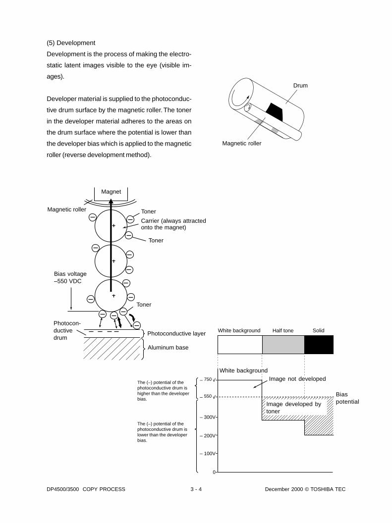
(5) Development
Development is the process of making the electro-
static latent images visible to the eye (visible im-
ages).
Developer material is supplied to the photoconduc-
tive drum surface by the magnetic roller. The toner
in the developer material adheres to the areas on
the drum surface where the potential is lower than
the developer bias which is applied to the magnetic
roller (reverse development method).
Photoconductive layer
The (–) potential of thephotoconductive drum ishigher than the developerbias.
The (–) potential of thephotoconductive drum islower than the developerbias.
Drum
Magnetic roller
Magnet
Magnetic roller Toner
Carrier (always attractedonto the magnet)
Toner
Bias voltage–550 VDC
Photocon-ductivedrum
Aluminum base
Toner
0
– 100V
– 200V
– 300V
– 400V
– 600V
White background Half tone Solid
White backgroundImage not developed
BiaspotentialImage developed by
toner
750
550

December 2000 © TOSHIBA TEC 3 - 5 DP4500/3500 COPY PROCESS
• Switching of developer bias polarity
With the area which has no negative change, back-
ground fogging is decreased by switching the bias
to the positive polarity (approx. +150V).
• Developer material
The developer material consists of a mixture of the
toner and carrier. The toner is charged to the negative
polarity and the carrier to positive polarity due to the
friction with each other caused by mixing.
Toner : Mainly consists of the resin and carbon.
Carrier : Consists of the ferrite and resin coating on
its surface to provide consistent frictional
electrification.
Note:
If the developer material is used for a long time
(beyond its normal life span),
the toner is caked onto the carrier.
x
The carrier’s (charging) performance is lowered.
Symptom: 1. Image density is lowered.
2. Toner scattering occurs.
3. Background fogging occurs.
Solution: Replace the developer material.
• Magnetic roller
- Magnetic brush development -
The south and north poles are arranged inside the
magnetic roller as shown in the right figure. The de-
veloper material forms a brush-like fluff which con-
tacts the photoconductive drum surface.
x
This is caused by the magnetic force lines between
the south and north poles.
Carbon(5~10%)
Resin (90~95%)
[Toner]
5~20µmFerrite
30~100µm
[Carrier]
TonerCarrier
No frictional electrificationoccurs on the area wherethe toner is caked on.
NSS
Magnetic forceline
Magnetic roller
Photoconductivedrum

DP4500/3500 COPY PROCESS 3 - 6 December 2000 © TOSHIBA TEC
Additional Explanation
The life of the toner cartridge (number of copies) varies depending on the following conditions.
1. Coverage of originals (printing image ratio of the original size) and density of original background
2. Size and density of originals
3. The existence of solid black when making copies (when a book is copied and the original cover is
partially opened)
4. Temperature and humidity in the room when making copies
5. Copy density and image quality mode
As indicated in the figure below, the life of the toner cartridge varies depending on the copy mode and
coverage of originals.
Type of originals
A.
B.
C.
AAAA
5,000
10,000
AAAA
AAAA
CCCC
15,000
BBBB
20,000

December 2000 © TOSHIBA TEC 3 - 7 DP4500/3500 COPY PROCESS
(6) Transfer
Transfer is a process of transfering the toner image
(visible image) formed on the drum surface onto
paper.
Method: A paper passing the side of the drum is
charged to the opposite polarity to the
toner's by the corona discharge of the
transfer charger.
x
The toner moves from the drum surface
onto the paper.
* For smooth transfer
In the transfer bias processing of this copier, bias
voltage (+580VDC) is applied to the pre-transfer
guide to prevent the charge produced by the trans-
fer charger from flowing into the pre-transfer guide
through the paper.
The corona discharge applied to the paper is nor-
mally 286µA DC. However, to improve transferabil-
ity at the trailing edge of the paper, lower output
(137µA DC) is applied to the part 10 mm from the
trailing edge.
(7) Separation
Separation is the process of separating paper which
is temporalily adhering to the drum due to the static
electricity during the transfer process.
Method: Apply AC voltage to which the negative
DC bias is added to the separation charger.
x
The positive charge on the paper is de-
creased.
x
The static electricity (adherence power) be-
tween the paper and drum becomes weak.
x
The paper is separated from the drum by
its own stiffness and absorption by the fan.
DrumPaper
Transfercharger
Toner
Drum rotation
Direction oftransportation
Transfer charger
Direction oftransportation
Drumrotation
Separation charger
Absorbing
Suction fan(Sub-separation fan)
u

DP4500/3500 COPY PROCESS 3 - 8 December 2000 © TOSHIBA TEC
* Output is controlled as follows to realizes the desirable separability and transferability.
Paper position against transfer point Separation output
From leading edge to 10 mm from leading edge (H) 4.8kV AC/–100 V DC
From 10 mm from leading edge to 17 mm from trailing edge (C) 4.5kV AC/–100 V DC
From 17 mm from trailing edge to trailing edge (L) 2.9kV AC/–100 V DC
Paper may not be separated from the drum
surface because of moisture or malfunction of
the transfer/separation charger. As the result,
the paper gets into the cleaner and causes
jamming. To prevent this, a separation finger is
used to forcibly separate the paper which was
left around the drum.
(8) Fusing
Fusing is the process of melting the toner on the
paper and fixing it firmly on the paper.
Method : The melting point of the toner (main in-
gredient : resin) is 100~110°C.
x
(Heat) Toner is melted by the heat of the sur-
face of the fuser roller.
+(Pressure) The pressure roller is pressed against
the fuser roller by the springs to increase
the adherence of the melted toner onto
the paper.
x
Heat and pressure are applied to the
paper when it passes between the fuser
roller and pressure roller.
||
(Fusing) The toner is fused on the paper.
Papermovement
IH coil
Fuser roller
Pressure roller
Separation finger
Separation finger
Drum rotation
Papermovement
Separationcharger
Fuser roller
Paper
Pressure
(Pressure)
Separation finger

December 2000 © TOSHIBA TEC 3 - 9 DP4500/3500 COPY PROCESS
(9) Cleaning
Cleaning is the process of removing the residual
toner from the photoconductive drum.
The edge of the urethane rubber cleaning blade is
pressed against the photoconductive drum surface
to scrape off the residual toner on it. The toner is
then caught by the recovery blade.
(10) Discharging
Discharging is the process of eliminating the negative
charge remaining on the photoconductive drum
before the next charging process.
If the residual charge is not eliminated, the follow-
ing phenomenon occurs:
Uneven charge is applied to the drum during the
next copying.
x
The next copy will have a double image. (The
preceding image appears.)
Solution :
The entire surface of the photoconductive drum
is illuminated with light by the discharge LED
array.
x
The photoconductive drum becomes electri-
cally conductive.
x
All of the negative charge remaining on the pho-
toconductive drum is conducted to the ground.
x
Preparation for the next copying is completed.
Discharge LED array
Photoconduc-tive drum
Ground
Cleaning blade
Drum rotation
Recovery blade

DP4500/3500 COPY PROCESS 3 - 10 December 2000 © TOSHIBA TEC
Process
1. Photoconductive drum
(1) Sensitivity
(2) Surface potential
2. Charging
3. Data writing(1) Light source
(2) Light amount
4. Development(1) Magnetic roller
(2) Auto-toner
(3) Toner supply
(4) Toner-empty detection
(5) Toner
(6) Developer material
(7) Developer bias
5. Transfer bias
6. Transfer
7. Separation
8. Discharge before cleaning
9. Discharge
(1) Discharging position
(2) Discharge lamp
10. Cleaning
(1) Method
(2) Recovered toner
11. Fusing(1) Method
(2) Cleaning
(3) Heater
3580 DP4500/3500
OD-2460 (OPC ø60) OD-3500 (OPC ø60)
Highly sensitized/durable drum Same as 3580
(Grid voltage –736 V) –750 V (grid voltage –790V)
Scolotron method (constant current) Same as 3580
Adjustable grid output (constant Same as 3580voltage)
Semiconductive laser (adjustment Same as 3580not required)
3.5 nJ/mm2 4.0 nJ/mm2
One magnetic roller Same as 3580
Magnetic bridge-circuit method Same as 3580
Toner cartridge Same as 3580
Density detection method Same as 3580
T-3580, T-3580E, T-3580D T-3500, T-3500E, T-3500D
D-3580 D-3500
DC–510V Adjustable output DC–550V Adjustable output(during printing) (during printing)
DC+150V (fixed) (others) DC+150V (fixed) (others)
Adjustment not required Same as 3580
Adjustable output (constant current) Same as 3580
AC:Adjustable output (constant Same as 3580current)
DC:Adjustment not required
AC:Adjustable output (constant Not availablecurrent)
DC:Adjustment not required
Exposure after cleaning Same as 3580
Red LED Same as 3580
Cleaning blade Same as 3580
Cannot be reused Same as 3580
Long-life fuser roller method Same as 3580•Fuser roller: •Fuser roller:Coated with fluoroplastic (ø40) Coated with fluoroplastic (ø40)
•Pressure roller: PFA tube roller (ø35) •Pressure roller: PFA tube roller (ø30)
•Cleaning roller for fuser roller (ø20) •Cleaning roller for pressure roller (ø14)
•Cleaning felt roller for fuser roller (ø18)
Halogen lamp (Lamp-heating method) IH coil (Induction-heating method)
Turned ON/OFF by thermistor Same as 3580
3.3 Comparison with 3580

December 2000 © TOSHIBA TEC 4 - 1 DP4500/3500 GENERAL OPERATION
4. GENERAL OPERATION
4.1 Overview of OperationOperation of copier Operation during initializing, pre-running and standby status
Cassette feed copying by START key
Copying operation Bypass feed copying
Interrupt copying
4.2 Description of Operation4.2.1 Warming-up
(1) Initialization
• Power is turned ON.
• The IH coil comes ON.
• Set number “1” and “WAIT WARMING UP” are displayed
• The fan motors are turned ON.
• Initialization of the scanner system
~ The carriages move to the home position.
~ The carriages move to the peak detection position.
~ The exposure lamp is turned ON. ~ Peak detection (white color is detected by the shading correc-
tion plate) ~ The exposure lamp is turned OFF.
• Set number “1” and “READY (WARMING UP)” are displayed.
(2) Pre-running operation
The pre-running operation is started when the temperature of the fuser roller reaches a certain
temperature.
• The fuser roller is rotated.
• The drum is rotated.
~ The main motor is turned ON.
• Initialization of laser optical system
~ The polygonal motor rotates at a low speed.
• Initialization of feeding system
~ Cassette trays go up.
• The pre-running operation is stopped after five seconds.
(3) When the temperature of the fuser roller becomes sufficient for fusing:
• Set number “1” and “READY” are displayed.

DP4500/3500 GENERAL OPERATION 4 - 2 December 2000 © TOSHIBA TEC
4.2.2 Standby state (ready for copying)
• Keys on the control panel operable
• When no key is pressed for a certain period of time:
~ Set number “1” and reproduction ratio “100%” are displayed. The copier returns to the normal
standby state.
4.2.3 Cassette feed copying
(1) Press START key
• “READY” changes to “COPYING”.
• The exposure lamp is turned ON.
• The scanner motor is turned ON n carriages -1 and -2 move forward.
• The main motor and exit motor are turned ON.
~ The drum, fuser unit, developer unit and exit roller are driven.
(2) Cassette paper feeding
• The main charger, developer bias and discharge lamp are turned ON. The fans rotate at high speed.
Feed clutch is turned ON.
~ The pickup roller, feed roller, separation roller and transport roller start to rotate.
• Paper reaches the upper feed sensor.
~ The upper feed sensor is turned ON.
• Paper reaches the registration roller.
~ The registration sensor is turned ON and aligning is performed.
• The feed clutch is turned OFF after a certain period of time.
(3) After the carriage operation:
• The registration clutch is turned ON after a certain period of time n paper is transported to the
transfer section.
• The copy counter operates.
(4) After the registration clutch is turned ON:
The transfer charger is turned ON after a certain period of time.
(5) Completion of scanning
• The scanner motor is turned OFF.
• The exposure lamp is turned OFF.
• The registration clutch is turned OFF (after the trailing edge of the paper passed the registration
roller).
• “READY (PRINTING)” is displayed.
(6) Paper discharging
• The exit sensor detects the trailing edge of the paper.
• The main charger, developer bias and discharge lamp are turned OFF.
• The main motor and exit motor are turned OFF.
• The drum, fuser unit and developer unit are stopped. The fans return to the standby rotation.
• “READY” is displayed and the copier enters the standby mode.

December 2000 © TOSHIBA TEC 4 - 3 DP4500/3500 GENERAL OPERATION
Timing in case of copying one A4 sized sheets fed from the upper cassette
500
0 6 18
246 36
6
1306
2316
1284
039
08
022
813
9823
94 2278
3378
4156
4296
042
96
2280
2246
2066
402
154
458
1658
1714
154
0
4156
1710
2296
1000
1500
2000
2500
3000
3500
4000
4500
5000
Sca
nner
m
otor
Exp
osur
e la
mp
Mai
n m
otor
Upp
er c
asse
ttefe
ed c
lutc
h
Upp
er f
eed
sens
or
Reg
istr
atio
n se
nsor
Reg
istr
atio
n cl
utch
MV
DE
N s
igna
l
Mai
n ch
arge
r
Dev
elop
er b
ias
Dis
char
ge l
amp
Exi
t se
nsor
(ms)
fwd.
rev. – +
DP4500/3500 GENERAL OPERATION 4 - 4 December 2000 © TOSHIBA TEC
4.2.4 Bypass-feed copying
(1) Insert some sheets of paper into the bypass tray.
• The bypass sensor comes ON.
~ “READY FOR BYPASS FEEDING” is displayed.
• The carriages move to the home position.
(2) Press START key
• “READY FOR BYPASS FEEDING” changes to “COPYING”.
• The exposure lamp comes ON.
• The scanner motor ON n Carriages -1 and -2 move forward.
• The main motor and exit motor are turned ON
~ The drum, fuser unit, developer unit and exit roller are driven.
(3) Bypass feeding
• The main charger, developer bias and discharge lamp are turned ON. The fans rotate at high speed.
• The bypass feed clutch is turned ON.
~ The bypass pickup roller and feed roller start to rotate.
~ The bypass pickup roller is lowered.
• Aligning operation
• Paper reaches the registration roller.
• The bypass feed clutch is turned OFF after a certain period of time.
(4) Hereafter, the operations (3) through (6) of “4.2.3. Cassette feed copying” are repeated.
4.2.5 Interruption copying
(1) Press the INTERRUPT key
• LED “INTERRUPT” is lit.
• Copying operation in progress is temporarily stopped, and the carriages -1 and -2 return to appropriate
positions.
• “JOB INTERRUPTED JOB 1 SAVED” is displayed.
• Automatic density and reproduction ratio 100% are set. The set number remains the same.
(2) Select the desired copy condition.
(3) After the interruption copying is finished:
• “PRESS INTERRUPT TO RESUME JOB 1” is displayed.
• LED “INTERRRUPT” goes OFF by pressing the INTERRUPT key, and the copier returns to the
status before the interruption.
• “READY TO RESUME JOB 1” is displayed.
(4) Press START key
The copying operation before the interruption is resumed.

December 2000 © TOSHIBA TEC 4 - 5 DP4500/3500 GENERAL OPERATION
4.3 Detection of AbnormalityWhen something abnormal occurs in the copier, the symbols corresponding to the type of abnormality are
displayed.
4.3.1 Types of abnormality
A) Abnormality cleared without turning off the door switch.
(1) Add paper
(2) Paper misfeed in bypass
B) Abnormality not cleared without turning off the door switch.
(1) Misfeed in copier
(2) Add toner
(3) Developer unit not installed properly
(4) Dispose of used toner
C) Abnormality not cleared without turning off the main switch.
(1) Call for service
4.3.2 Description of abnormality
A-1) Add paper
[In case of the copier cassette or PFP cassette] (When cassette is not installed)
Cassette not detected
Cassette is not installed
or
Cassette is installed but
there is no paper in it:
n No paper
x
A signal is sent to the control circuit.
x
Cassette in question flashes on the control panel.
x
START key is disabled.
[In case of the copier cassette, PFP cassette or LCF cassette] (When cassette is installed)
Based on the combination of the tray-up motor movement and the state of the tray-up sensor and
paper-empty sensor, the CPU detects the presence/absence of paper.

DP4500/3500 GENERAL OPERATION 4 - 6 December 2000 © TOSHIBA TEC
• When the power is turned ON or the LCF cassette is inserted (when the power is turned ON or copier
cassette/PFP cassette is inserted),
LCF performs initialization.
x
Detects the presence/absence of paper
Tray-up motor ON ~ The tray goes up
At this time, the tray-up sensor and LCF empty sensor are OFF.
bbn If the tray-up sensor is not turned ON in a fixed time, the tray is in abnormal condition.
n “Add paper” is displayed regardless of presence/absence of paper.
qax
Cleared by turning ON and OFF the power
bbn Tray-up sensor is turned ON in a fixed time.
~ The tray-up motor stops.
At this time, if the empty sensor is ON: It is judged that there is paper.
At this time, if the empty sensor is OFF: It is judged that there is no paper.
x
Cassette in question flashes on the control panel.
• When paper in the cassette gets short during copying,
The tray-up sensor is turned OFF.
n The tray-up motor is turned ON. n The tray goes up.
The tray-up sensor is turned ON. n The tray-up motor is stopped.
• The empty sensor is turned OFF during the copying in spite of the tray-up sensor being ON
It is judged that there is no paper.
x
Cassette in question flashes on the control panel.
x
The copying operation is stopped.

December 2000 © TOSHIBA TEC 4 - 7 DP4500/3500 GENERAL OPERATION
A-2) Paper misfeed in bypass ( )
• During the bypass feeding
The bypass feed clutch is turned ON.
x
The registration sensor is turned ON.
* The registration sensor is not turned ON in a fixed time (E12).
x
Bypass misfeeding
x
The bypass misfeeding symbol ( ) is displayed.
x
The copying operation is disabled.
x
Solution: The bypass paper sensor is turned OFF by removing the paper from the bypass tray.
B-1) Misfeed in copier ( )
• The exit sensor detects that the leading edge of paper is jamming.
x
The registration clutch is turned ON.
x1.056 sec.
The exit sensor is turned ON.
If the exit sensor is not turned ON even though
1.056 seconds have elapsed,
x
Paper jam (E01) n The copying operation is stopped.
• The exit sensor detects that the trailing edge
of paper is jamming.
x
The registration clutch is turned OFF.
x 1.116 sec.
The exit sensor is turned OFF.
If the exit sensor is not turned OFF even though
1.116 seconds have elapsed,
x
Paper jam (E02) n The copying operation is stopped.
• Immediately after the power comes ON
x
Any of the sensors to detect a paper which is tranported on the transport path detects the presence
of a paper (ON).
x
Paper jam (E03)
Registration clutch
Exit sensor
Timer0
Paper jam (E01)
ON
ON
1.056sec.
Registration clutch
Exit sensor
Timer0
Paper jam (E02)
ON
OFF
1.116sec.

DP4500/3500 GENERAL OPERATION 4 - 8 December 2000 © TOSHIBA TEC
• The front cover is opened during copying.
x
Paper jam (E41)
• The registration sensor detects that the leading edge of paper is jamming.
x
The registration sensor is not turned ON in a fixed time after the leading edge of paper passed the
transport roller.
x
Paper jam (E12, E20, E21, E30, E33 and E3C)
• When paper is fed from the ADU:
The registration sensor is not turned ON in a fixed time after the ADU clutch is turned ON.
x
Paper jam (E11)
• When paper is transported into/from ADU:
The ADU entrance/exit sensors do not detect the paper at the fixed timing.
x
Paper jam (E51 or E52)
• When paper is fed from the main unit or PFP cassette:
The registration sensor is not turned ON in a fixed time after the feed clutch is turned ON.
x
Paper jam (E22, E31, E32, E34~E36, E3D and E3E: Error code defers depending on the paper
source.)

December 2000 © TOSHIBA TEC 4 - 9 DP4500/3500 GENERAL OPERATION
B-2) Add toner ( )
The toner density becomes low.
x
The auto-toner sensor detects the absence of the toner.
x
Control circuit n “Add toner” displayed: the copying operation disabled.
Solution: Open the front cover and replace the toner cartridge with a new one.
Toner supplied n copying operation enabled.
B-3) Developer unit not installed properly
The connector of the developer unit is disconnected.
x
“Developer unit not installed” displayed.
Solution: Connect the connectors of the developer unit and close the front cover.
B-4) Dispose of used toner ( ).
• The toner bag becomes full of toner.
x
The toner recovery auger moves towards the rear of the copier: the toner bag full detection sensor is
turned ON.
x
“Dispose of used toner” is displayed.
• When the toner bag full detection sensor is turned ON.
x
Copying operation is disabled after the sheet which is being copied is discharged in the paper
receiving tray.
Solution: Replace the toner bag with a new one.
C-1) Call for service
An error code is displayed instead of the set number by pressing the CLEAR/STOP key and “8” key
simultaneously when “Call for service” is flashing.
Refer to the error code table in the Service Handbook.

DP4500/3500 GENERAL OPERATION 4 - 10 December 2000 © TOSHIBA TEC
4.4 Flow Chart4.4.1 Immediately after the power is turned ON
YES
YES
NO
A B
NO
NO
NO
NO
NO
NO
NO
NO
YES
YES
YES
YESCall for service
YES
YES
YES
“E03”
“C26”
“C27”“C28”
Main switch ON
DC power ON
Restart
Cover is open?
IH coil ON
Paper jam
Registration sensorON? Scanner motor ON
Home positiondetected?
Peak detected?
2.5 seconds elapsed?
Call for service
Exit sensorON?
ADUentrance/exit sensors
ON?
Upper feedsensor ON?
Lower feedsensor ON?
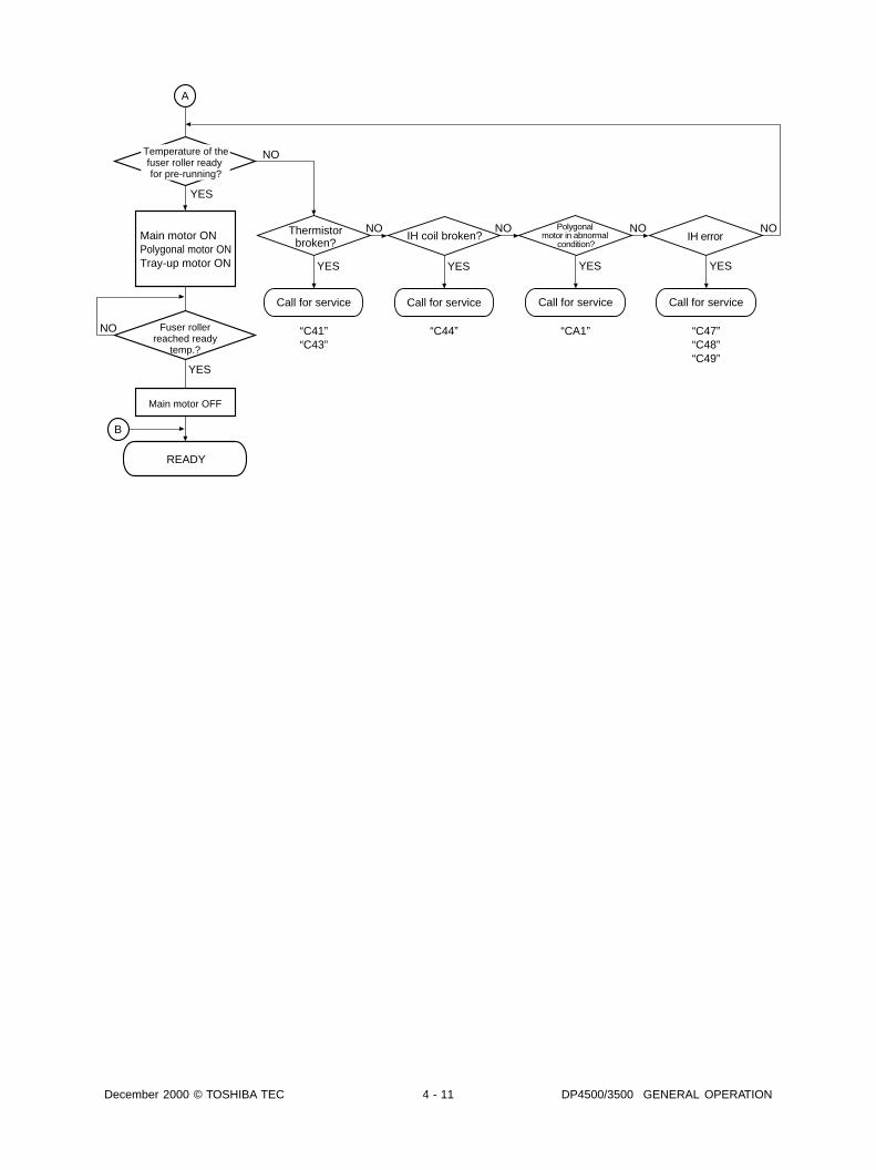
December 2000 © TOSHIBA TEC 4 - 11 DP4500/3500 GENERAL OPERATION
YES
YES
NO
A
B
Main motor ONPolygonal motor ONTray-up motor ON
Fuser rollerreached ready
temp.?
Main motor OFF
READY
YES
Call for service
YES
Call for service
IH coil broken?
YES
Polygonal motor in abnormal
condition?
Call for service
NO
NO
NO NO
“C41”“C43”
“C44” “CA1”
YES
IH error
Call for service
NO
“C47”“C48”“C49”
Thermistorbroken?
Temperature of thefuser roller ready for pre-running?

DP4500/3500 GENERAL OPERATION 4 - 12 December 2000 © TOSHIBA TEC
4.4.2 Automatic paper feed copying
OK
NO
NO
Main motor ONExit motor ON
Developer bias ONMain charger ONDischarge lamp ON
Remaining set number=0?
Press START key
Transport system control
YES
YES
YES
NO
NO
NG
Laser ON
Remaining setnumber=0?
Processing systemcontrol completed
H-SyncOK?
Processing system control
Call for service
Polygonal motornormal rotation?
“CA1”
Transfer charger ON
Transfer charger OFF
Feed clutch ON
Feed clutch OFF
Registration clutch ONCounter ON/OFF
Registration clutch OFF
Call forservice
Laser OFF
C
Scanner system control
Exposure lamp ON
Carriages move forward
Carriages stopped
Exposure lamp OFF
Carriages move backward
Carriages stopped
Scanner system control completed
“E01”
YES
“CA2”
Paper jam
Exit sensordetected leading edge of paper?

December 2000 © TOSHIBA TEC 4 - 13 DP4500/3500 GENERAL OPERATION
OK
NG
C
Main charger OFFDischarge lamp OFFDeveloper bias OFFExit motor OFF
Standby
Drum rotation reversed
Main motor OFF
Paper jam
“E02”
Exit sensordetected trailing edge of paper?

DP4500/3500 GENERAL OPERATION 4 - 14 December 2000 © TOSHIBA TEC

December 2000 © TOSHIBA TEC 5 - 1 DP4500/3500 DISPLAY UNIT
5. DISPLAY UNIT
5.1 Control Panel and Display PanelThe display unit consists of key switches and touch-panel switches to operate the copier and select
various modes, and LEDs and an LCD to display the state of the copier or the messages.
When the operator’s attention is reguired, graphic symbols appear with messages explaining the condition
of the copier in the LCD panel.
Control panel
PRINTER/NETWORK COPY FAX
1
1
2 3
4 5 6
7 8 9
0JOB STATUS
START
CLEAR/STOP
FUNTION CLEAR
INTERRUPT
MAIN POWER
POWER
MONITOR//PAUSE
MEMORY RXDATAERROR
ABC DEF
JKLGHI MNO
TUVPQRS WXYZ
2
C/
FC
HELP

DP4500/3500 DISPLAY UNIT 5 - 2 December 2000 © TOSHIBA TEC
5.2 Items Shown on the Display Panel
Fig. 5.2-1
Fig. 5.2-2
CA
E
I
D
FK
G
J
H
B

December 2000 © TOSHIBA TEC 5 - 3 DP4500/3500 DISPLAY UNIT
No. Message
1 WAIT WARMING UP
2 READY(WARMING
UP)
3 READY
4 COPYING
5 Saving energy
- press START
6 Place next original
Press START to
copy
7 -
8 READY (PRINTING)
9 READY
(ADD PAPER)
10 READY
(FINISHER FULL)
11 READY
(HOLE PUNCH
DUST FULL)
State of copier
Scanner warming up
- Displayed when the power is turned ON un-
til the copier becomes ready to start scan-
ning.
Ready for scanning
- The copier is ready for scanning and waiting
for operator to select the copying conditions.
- Returns to default setting if no key is pressed
within 45 seconds.
Ready for copying
- The copier is ready for copying and waiting for
the operator to select the copying conditions.
- Returns to default setting if no key is pressed
within 45 seconds.
The original is being scanned
- Displayed by pressing the START key.
The copier is in the energy saver mode
Ready for the next original
- Displayed by pressing the [Next original;
YES] icon.
Power is OFF
- Nothing is displayed in the display panel.
- Power LED is lit in red.
Ready for scanning
- The copier is ready for scanning and waiting
for the operator to select the copying conditions.
Background printing is in progress
Ready for scanning
- The copier is ready for scanning and waiting
for the operator to select the copying conditions.
Paper in the cassette has run out during printing
Ready for scanning
- The copier is ready for scanning and waiting
for the operator to select the copying conditions.
The finisher is full of paper
Ready for scanning
- The copier is ready for scanning and waiting
for operator to select the copying conditions.
The punching dust box is full
Note
- The set number “1” and the repro-
duction ratio “100%” are displayed
when the power is turned ON.
- The set number “1” is displayed. Press
the digital key to change the number.
- The number is reset to “1” by pressing
the CLEAR/STOP key.
- Bypass feed copying is enabled.
- The set number “1” is displayed. Press
the digital key to change the number.
- The number is reset to “1” by pressing
the CLEAR/STOP key.
- Bypass feed copying is enabled.
- After scanning is completed, the copier
becomes ready for the next scanning.
- Can be cleared by pressing the
START key or FUNCTION key.
- Displayed for SADF and manually
placed originals.
- Press the POWER key.
- Since background printing is in
progress, the scanned image is not
output immediately.
- Printing is resumed by adding paper
to the cassette.
- Printing is resumed by removing
paper from the finisher.
- Printing is resumed by removing
punching dust from the dust box.
5.2.1 Display during normal copying

DP4500/3500 DISPLAY UNIT 5 - 4 December 2000 © TOSHIBA TEC
No. Message State of copier Note
12 READY
(SADDLE STITCH
TRAY FULL)
13 READY
(SET CORRECT
CASSETTE)
14 READY (ADDING
TONER)
15 READY (INSIDE
TRAY FULL)
16 READY (CHECK
STAPLER)
17 READY (CHECK
SADDLE STITCH
STAPLER)
18 READY (USE
GENUINE TOSHIBA
TONER)
19 ENTER DEPART-
MENT CODE
Ready for scanning
- The copier is ready for scanning and waiting
for the operator to select the copying conditions.
The saddle stitcher is full of paper
Ready for scanning
- The copier is ready for scanning and waiting
for the operator to select the copying conditions.
Cassette not installed during printing
Ready for scanning
- The copier is ready for scanning and
waiting for the operator to select the
copying conditions.
The toner is being added from the cartridge
Ready for scanning
- The copier is ready for scanning and waiting
for the operator to select the copying
conditions.
The receiving tray is full of papers
Ready for scanning
- The copier is ready for scanning and waiting for
the operator to select the copying conditions.
The finisher unit runs out of the staples.
Ready for scanning
- The copier is ready for scanning and
waiting for the operator to select the
copying conditions.
The saddle stitcher unit runs out of the
staples
Ready for scanning
- The copier is ready for scanning and
waiting for the operator to select the
copying conditions.
Toner other than Toshiba’s has been used
The copier is waiting for the operator to
enter the department code.
- Displayed when the department manage-
ment function has been used.
Printing is resumed by removing paper
from the saddle stitcher unit.
- Printing is resumed by changing
the setting for cassette selection,
then pressing the START key.
- Printing is resumed automatically
when the toner supply is completed.
- Printing is resumed automatically
when the paper is removed from
the receiving tray.
- Printing is resumed automatically
when the staple cartridge is
replaced with a new one.
- Printing is resumed automatically
when the staple cartridge is
replaced with a new one.
The display is made to disappear by
using the toner provided by Toshiba.
The copier becomes ready to start
copying when the correct depart-
ment code is entered.

December 2000 © TOSHIBA TEC 5 - 5 DP4500/3500 DISPLAY UNIT
No. Message
20 Add paper
21 Add toner
Press HELP/INFO
22 Set key copy
counter
23 Paper misfeed in
bypass
24 Misfeed in copier
Press HELP/INFO
25 Misfeed in copier
Press HELP/INFO
26 Misfeed in doc.
feeder
Press HELP/INFO
27 Misfeed in finisher
Press HELP/INFO
28 Misfeed in duplexer
Press HELP/INFO
29 Call for service
30 Time for periodic
maintenance
31 CHECK PAPER IN
LCF
32 Dispose of used
toner
Abnormal state and indication in display panel
Paper run out [Fig.5.2-1 A]
- The cassette with no more paper flashes.
Toner run out [Fig.5.2-2 B]
- The toner cartridge is empty.
- The message is displayed and the copier is
stopped.
Key copy counter not installed [Fig.5.2-1 C]
- The key copy counter was pulled out when
copier was ready for scanning.
- When the key copy counter is pulled out af-
ter the START key is pressed, the copier is
stopped as soon as the copying is finished.
Bypass paper jam [Fig.5.2-2 D]
- Paper jam at the bypass tray
Paper jam in the copier [Fig.5.2-2 E]
Misfeeding of cassette paper [Fig.5.2-2 F]
- Paper fed from the cassette does not reach
the feed sensor in a fixed time.
Original jam [Fig.5.2-2 G]
- Original jamming in ADF
Paper jam in the finisher [Fig.5.2-2 H]
Paper jam in the ADU [Fig.5.2-2 I]
Motors, sensors, switches, etc. do not work
properly. [Fig.5.2-2 J]
PM cycle
- Time for maintenance
- Copying is possible
Paper misloading in LCF
- Paper is not stacked up correctly.
Toner bag full
- The toner bag is full of used toner.
The copier stops its operation. [Fig.5.2-2 K]
Solution
- Add paper to the cassette.
- Select a different cassette.
- Replace the toner cartridge and close
the front door.
- Insert the key copy counter (option).
- Remove the paper from the bypass
tray.
- Press the HELP/INFO key and re-
move the paper following the mes-
sages shown on the display panel.
- Press the HELP/INFO key and re-
move the paper following the mes-
sages shown on the display panel.
- Open the jam-access cover and ADF
unit to remove the original.
- Press the HELP/INFO key and re-
move the paper following the mes-
sages shown on the display panel.
- Press the HELP/INFO key and re-
move the paper following the mes-
sages shown on the display panel.
- Turn OFF the power and solve the
problem, then turn ON the power again.
- Maintenance and inspection are per-
formed by a qualified service techni-
cian.
- Set the paper correctly.
- Replace the toner bag with a new
one and close the front cover.
5.2.2 Display in the abnormal condition

DP4500/3500 DISPLAY UNIT 5 - 6 December 2000 © TOSHIBA TEC
5.3 Relation between Copier State and Operator’s ActionO
pera
tion
STA
RT
C/S
Dig
ital
Cas
sette
INTE
RR
UPT
PO
WE
RB
ypas
sTo
uch
FUN
CTI
ON
CO
ND
ITIO
N
Sta
te o
f co
pier
key
key
keys
sele
ctio
nke
yke
yfe
edin
gp
an
el
key
key
Sca
nner
war
min
g up
--
--
Prin
ter
war
min
g up
Rea
dy f
or c
opyi
ng
Pri
ntin
g
Sca
nn
ing
--
--
--
--
Pap
er r
un o
ut
Tone
r em
pty
Key
cop
y co
unte
r no
t in
sert
ed-
(opt
iona
l)
Pap
er m
isfe
ed i
n by
pass
cop
ying
--
--
--
--
--
Pap
er ja
mm
ed in
side
the
mac
hine
--
--
--
--
--
Ser
vice
cal
l in
dica
ted
--
--
--
--
--
Rea
dy f
or i
nter
rupt
cop
ying
--
In e
nerg
y sa
ver
mod
e-
--
--
--
Pow
er O
FF
--
--
--
-
: O
pera
tion
enab
led
-
: Ope
ratio
n di
sabl
ed

December 2000 © TOSHIBA TEC 5 - 7 DP4500/3500 DISPLAY UNIT
5.4 Description of Operation5.4.1 Dot matrix LCD circuit
(1) Structure
The DSP-LCD-320 is an STN blue mode transmissive type LCD with a 320 x 240-dot display capacity. It
consists of a driver LSI, frame, printed circuit board, and lateral type CFL backlight.
*STN:Super Twisted Nematic
(2) Block diagram
(320 x 240)
IC1
IC5
XSCL
UD0UD1UD2UD3
WF
LP
VDDGNDV0VEE
Power supply
LCDEN
IC6
IC7
IC2
LCD PANEL320 x 240 DOTS
IC3 IC4
80
80
80
80 80 80 80

DP4500/3500 DISPLAY UNIT 5 - 8 December 2000 © TOSHIBA TEC
(4) Data Transmission
(3) LCD drive operation
The following describes the drive operation to display the message “READY”.
(a) The SYS CPU requests the PROM
data to display “READY”.
(b) The PROM outputs data to display
the message to the SYS CPU.
(c) The SYS CPU writes the data to be
displayed on the LCD into the RAM.
(d) The LCD controller/driver reads the
display data from the RAM, and out-
puts the data to the LCD.
PROMCPU
RAM
LED
LED LCD KEY CPU
PWA-F-DSP-300
PWA-F-SYS-300
GA
LCD
SYS(a)
(b)(c)
(c)
(d)
(d)
LOAD
FRAME
LOAD
240 1 2 240
CP x(320/4) pulses
1 2 240
1/tF1/tF
1 2
FRAME
D0-D3
CP
controller
driver
PWA-F-SYS-320
PWA-F-DSP-320
Key switchesand
touch panel

December 2000 © TOSHIBA TEC 5 - 9 DP4500/3500 DISPLAY UNIT
LDON0"L"
"L" 17D7
Q3
IC8(7932)
R6(COPY)
5VL
LED5
G
5.4.2 LED display circuit
(1) Method of LED display
ex) Displaying “COPY” .
The transistor is turned ON when the LDON 0 signal becomes “L” level.
Also, when IC8-17pin (D7) changes to “L”, the current flows from 5VL via the transistor to LED5 (“COPY”)
to turn ON LED5 (“COPY”).
Current
Conditions to turn ON the LED
(a) The transistor (Q3) connected to the LED anode is ON.
(b) The output from the cathode side of the LED is “L” level.
The LED is turned ON when (a) and (b) are satisfied.

DP4500/3500 DISPLAY UNIT 5 - 10 December 2000 © TOSHIBA TEC
(5) Remove 4 screws and take off the LCD board.
(6) Remove 11 screws and take off the KEY board.
5.5 Disassembly and Replacement[A] Control panel
(1) Take off the front side right cover, front top cover
and control panel lower cover.
(2) Disconnect one connector and remove 5 screws.
Take off the control panel unit.
(3) Remove 6 screws and take off the 3 brackets.
(4) Disconnect 6 connectors and remove 2 screws.
Release 6 lock supports and take off the DSP
board.
Control panel unit
Connector
Lock support
DSP board Lock support
KEY board LCD

December 2000 © TOSHIBA TEC 6 - 1 DP4500/3500 IMAGE PROCESSING
6. IMAGE PROCESSING
6.1 General DescriptionThe following diagram shows the process from scanning of the original to data writing on the photoconduc-
tive drum surface of the digital copier.
ASIC stands for “Application Specific IC”, meaning an IC designed for a particular use.
The followings are the boards used for image processing.
Board Number of ASIC Function
CCD board
(PWA-F-CCD-320)1
LGC board1
(PWA-F-LGC-320)
Image processing/writing control
section[LGC]
Image processing section
Photocon-ductivedrum
System board[SYS]
Scanningcontrol section
[SLG]
Scanning section
Original
Original glass
Scanning/image process-
ing section[CCD]
Semicon-ductive laserelement
Laser drive board[LDR]
Writing section
Polygonal motordrive board
[POL]
High-quality image processing, image memory editing, editing
processing, gamma correction, gradation processing, external
output system interface
Smoothing processing, external input system interface, image area
control, laser related control

DP4500/3500 IMAGE PROCESSING 6 - 2 December 2000 © TOSHIBA TEC
6.2 Image Processing Circuit6.2.1 General description
The image of an original placed on the original glass is scanned by the carriage. The CCD (Charge Coupled
Device) reads the optical image signals and converts them into the electrical signal. The electrical signals
then undergo the analog-to-digital conversion and are changed into digital signal. The shading correction
(correction of variance in CCD elements and the light source) is performed on the digital signal, then it is
output as an image signal from the scanning section.
The image processing section inputs this image signal from the scanning section and applies various
types of image processing on it, then sends the output result to the writing section.
Images are processed by the CCD board (PWA-F-CCD-320), SLG board (PWA-F-SLG-320) and LGC
board (PWA-F-LGC-320) in this copier.
(1) Image processing circuit on the CCD board
One image processing ASIC is mounted on the CCD board, realizing the following functions:
<Functions>
High-quality image processing, image memory editing, edit processing, gamma correction,
gradation processing and external output system interface
(2) Image processing circuit on the LGC board
One image processing ASIC is mounted on the LGC board, realizing the following functions:
<Functions>
Smoothing processing, external input system interface, image area control and laser related control

December 2000 © TOSHIBA TEC 6 - 3 DP4500/3500 IMAGE PROCESSING
6.2.2 Configuration
The following diagram shows the image processing section of this copier.
Fig. A. Configuration of the image processing section
CCD board(PWA-F-CCD-320)
CCD
A/D conversion
Image processing ASIC for Scanner section
Shading correctionHigh-quality image processing
Image memory editingEditing processingGamma correction
Gradation processingExternal output system interface
SLG board(PWA-F-SLG-320)
SYS board(PWA-F-SYS-320)
Sorting, group copy, magazinecopy, single side reduction/con-junction, double side reduction/conjunction, image composition,date insertion, sheet insertionmode, etc.
Scanner CPU
Scanning control
LGC board(PWA-F-LGC-320)
Image processing ASIC for Printer sction
Smoothing processingExternal input system interface
Image area controlLaser related control
Main CPU
Laser writing control
Laser drive board(PWA-F-LDR-320) : Image data flow
Image processingsection
Laser drive

DP4500/3500 IMAGE PROCESSING 6 - 4 December 2000 © TOSHIBA TEC
6.3 CCD Board (PWA-F-CCD-320)6.3.1 Features
(1) The image processing ASIC on the CCD board is controlled by the CPU on the SLG board.
(2) The image processing ASIC on the CCD board realizes the following functions:
• High-quality image processing
• Image memory editing
• Editing processing
• Gamma correction
• Gradation processing
• External output system interface
6.3.2 Functions of image processing circuit
An image processing ASIC mounted on the CCD board realizes the following functions:
(1) High-quality image processing
(a) Range adjustment
This function converts the image signals into a density range, and adjusts it so that it is suited to each
original image. It is possible to eliminate undesirable background density when an original with a certain
level of density on the background, for example a newspaper, is copied.
<Example>
Histogram
Dynamic range
Sm
all
No.
of p
ixels
Larg
e
Low Density
High Low Density
High
Text
Back-ground
After rangeadjustment
Extended dynamic range
Sm
all
No.
of p
ixels
Larg
e

December 2000 © TOSHIBA TEC 6 - 5 DP4500/3500 IMAGE PROCESSING
0 1 2 3 4 5 6 7 8 9 0 1 2 3 4 5 6 7 8 9
(b) Filtering
This function is enabled by a low-pass filter circuit and a high-pass filter circuit.
• Low-pass filter circuit
This circuit removes image noise and electrical noise, decreases moire, and realizes high
reproductibility of original by applying an averaging operation on the image signal of the targeted
pixel and those of the pixels positioning next to it.
<Example> The density of the targeted pixel position is “x”. The density of the pixel positions at
the front and back of the targeted pixel are “a” and “b” respectively, “x” is converted to
“x’” through low pass filtering.
When the matrix is (3 x 1):
The above averaging operation is performed for all the pixel positions to accomplish the high
reproducibility of the original.
The following is when low pass filtering is applied on the primary scanning pixel.
(b) High-pass filter circuit
The change of the density at the character outline becomes smooth when an original, such as text,
with a great difference in density between the pixels placed next to one another is optically scanned
and output from the CCD. This is caused by the characteristic of the lens and other factors. In this
copier, the process such as the edge enhancement, is applied on the targeted pixel and the pixels
around it to eliminate this phenomenon and realize high reproductibility of the original.
Density
After low-pass filtering
Primary scanning pixel positions
a + b + x3
x’ =
Original
Image signal
After correction
Low contrast area
Solid black area
Density
Primary scanning pixel positions
a x b

DP4500/3500 IMAGE PROCESSING 6 - 6 December 2000 © TOSHIBA TEC
(2) Image memory editing
This function performs editing such as enlargement/reduction, mirror imaging, etc. using the line memory.
Pixel data for one line in the primary scanning direction are stored in the line memory and the memory
is renewed at each line.
(a) Enlargement/reduction
The enlargment/reduction is accomplished by using the line memory control function in the process
of the image processing operation.
<Example> Enlargement
<Example> Reduction
(b) Mirror imaging
This is accomplished by reading and outputting data from its end.
(3) Edit processing
This function performs trimming, masking and negative/positive reversing.
(a) Trimming
Using rectangular area signals, the image signals inside the rectangular area are left and the
other image signals outside the area are eliminated.
(b) Masking
Using rectangular area signals, the image data inside the rectangular area are erased.
(c) Negative/positive reversing
This function reverses the entire data from negative to positive or vice versa.
1100%
200%
2 3 4 5 6 7 8 9 10
1 1 2 2 3 3 4 4 5 5
1100%
50%
2 3 4 5 6 7 8 9 10
1 3 5 7 9

December 2000 © TOSHIBA TEC 6 - 7 DP4500/3500 IMAGE PROCESSING
(4) Gamma correction
This function corrects the input/output characteristics of the scanner/printer and adjusts the image
signals so that their input/output characteristics match with the copy mode.
(5) Gradation processing
This function works for genuine reproduction of halftone image such as photographs.
(6) External output system interface
This function controls the output of the output interface between the CCD board and the SYS board
(PWA-F-SYS-320).

DP4500/3500 IMAGE PROCESSING 6 - 8 December 2000 © TOSHIBA TEC
6.4 LGC Board (PWA-F-LGC-320)6.4.1 Features
(1) The image processing ASIC on the LGC board is controlled by the CPU on the LGC board.
(2) The image processing functions of the LGC board realizes the following functions:
• Smoothing processing
• External input system interface
• Image area control
• Laser related control
6.4.2 Functions of image processing circuit
An image processing ASIC mounted on the LGC board enables the following functions:
(1) Smoothing processing
This function removes jagginess and smoothes character outline of the text images input from the
external input system interface, and output them.
(2) External input system interface
This function controls the input interface between the LGC board and the SYS board (PWA-F-SYS-
320).
(3) Image area control
This function sets the effective image area of four directions for the image to be output.
(4) Laser related control
This function controls the APC (Auto Power Control).

December 2000 © TOSHIBA TEC 6 - 9 DP4500/3500 IMAGE PROCESSING
6.5 Scanning SectionLight reflected from original surface is directed to the CCD which performs the photovoltaic conversion,
and the optical image data are converted into an electrical signal. This analog signal undergoes the A/D
conversion processing and is changed into a digital signal. The signal then undertakes various corrective
processes necessary for image formation.
(1) Photovoltaic conversion
The CCD elements convert the optical signal into electrical signal. ( Chapter 7.6.1)
(2) Signal amplification
Amplifies the electrical signals converted in the CCD.
(3) A/D conversion
Converts the analog signal into the digital signal.
(4) Shading correction
The shading correction is applied on the signal read by CCD. ( Chapter 7.6.2)
6.6 Writing SectionThe image signal processed by the LGC board is processed by the ASIC for writing control and laser drive
board. The laser is controlled based on the signal, writing data on the drum.
(1) Setting the effective image area........................ • Top, bottom, left and right margins
(2) Horizontal synchronization signal (H-Sync) ....... • The reference clock signal in the printer section
clock generation section synchronized with the H-Sync and its signal.
(3) Laser drive section ........................................... • ON/OFF control of the semiconductive laser and
APC (Auto Power Control) control.
CCDSignal
amplificationA/D
conversionShading
correction Next stage

DP4500/3500 IMAGE PROCESSING 6 - 10 December 2000 © TOSHIBA TEC

December 2000 © TOSHIBA TEC 7 - 1 DP4500/3500 SCANNER
Exposure lamp
Carriage-2
Reflector Carriage-1 Original glassRail for carriage-1 Drive pulley
LensCCD sensor CCD board SLG board
Rail for carriage-2
7. SCANNER
7.1 FunctionIn the scanning section of this copier, the surface of an original is irradiated with a direct light and the
reflected light is led through mirrors, lens and slit to the CCD where the optical-to-electrical conversion is
performed, converting the optical image data into an electrical signal. This analog signal is changed to a
digital signal, and then undertakes various corrective processes necessary for image formation. After that,
an arithmetic operation is performed on the digital signal, which is then sent to the data writing section.
Shading correction plate

DP4500/3500 SCANNER 7 - 2 December 2000 © TOSHIBA TEC
7.2 ConstructionThe construction and purpose of the scanning system are described in this section.
(1) Original glass
This is the glass on which originals to be copied are placed. The light from the exposure lamp is irradiated
to the original through this glass.
(2) Carriage-1
The carriage-1 consists of the exposure lamp, lamp inverter, reflector, mirror-1, etc. It is driven by the
scanner motor and scans the original on the glass.
Mirror-1
a. Exposure lamp
This lamp is the light source to irradiate the original on the glass (one 20W Xenon lamp).
b. Lamp inverter
Controls lighting of the Xenon lamp.
c. Reflector
This is a plate to direct the light from the exposure lamp efficiently to the surface of the original on the
glass.
Lamp inverterReflector
OriginalOriginal glass
Exposure lamp
Reflector
Mirror-1

December 2000 © TOSHIBA TEC 7 - 3 DP4500/3500 SCANNER
d. Mirror-1
This mirror directs the light reflected from the original to the mirror-2 described later.
(3) Carriage-2
The carriage-2 consists of mirror-2, mirror -3, etc. and directs the reflected light from the mirror-1 through
mirrors-2 and -3 to the lens.
This carriage is driven by the scanner motor as the carriage-1, at half the scanning speed of carriage-1 (the
scanning distance is also half that of carriage-1).
Mirror-2
Mirror-3

DP4500/3500 SCANNER 7 - 4 December 2000 © TOSHIBA TEC
(4) Lens unit
The light reflected from mirror-3 is led to the CCD placed at the focal point of the lens which is fixed in
position.
(5) CCD drive PC board
Processes such as the signal amplification, signal integration, A/D conversion and shading correction are
applied on the electrical signal which was converted by the CCD.
(6) Automatic original detection sensor
The size of the original placed on the glass is instantly detected using the automatic original detection
sensors (APS sensor) fixed on the base frame without carriage-1 having to move.
CCD drive PC boardLens unit

December 2000 © TOSHIBA TEC 7 - 5 DP4500/3500 SCANNER
Carriage-1Carriage wire Scanner motor Pulley for carriage-2ø20
Idler pulleyø20
Wire winding-up pulley/motor speed-reduction pulley
ø39/2GT-Z63Carr iage-2CRG2
Idler pulleyø20
Motor pulley2GT-Z21
7.3 Description of Operation7.3.1 Scanner motor
(a) Scanning an original placed on the original glass
This motor drives the carriages-1 and -2 through the timing belt and carriage wire. The scanner motor
first drives carriages-1 and -2 to their respective home positions. The home positions are detected
when carriage-1 passes the home position sensor. When the START key is pressed, both carriages
start to move and scan the original on the glass.
(b) Scanning an original placed on the ADF
Carriage-1 stays at the shading position during the shading correction, and at the scanning position
during the scanning operation.

DP4500/3500 SCANNER 7 - 6 December 2000 © TOSHIBA TEC
7.3.2 Two-phase motor drive circuit (fixed-current type)
The scanner motor is driven by the stepping motor driver IC-STK672-080 (IC1) with the unipolar fixed
current chopper method.
15141312111098
67
EN
AB
LEMol
RE
SE
T
M3
CLO
CK
CW
B
M2
M1
Vcc
2V
ref
AA
BB
BB
PG
SU
B
54
32
1
Exc
itatio
nm
ode
setti
ng
Switc
hing
pul
seO
N/O
FF d
etec
tion
Exc
itatio
nst
atus
mon
itor
CR
osc
illat
ion
Pha
seco
unte
r
Gen
erat
ion
ofre
fere
nce
clock
PWM
cont
rol
Gen
erat
ion
of p
hase
excit
atio
n sig
nal
Gen
erat
ion
of p
seud
osi
ne w
ave
Switc
hing
curre
ntfra
ctio
n ra
tio

December 2000 © TOSHIBA TEC 7 - 7 DP4500/3500 SCANNER
The motor is rotated by setting the number of pulses.
* The internal circuit of the motor driver works when the first pulse
becomes ON and the last pulse becomes OFF.
The direction of the motor rotation is determined by the setting level
of signal
“H”…Clockwise direction (as seen from the output shaft)
“L”…Counterclockwise direction (as seen from the output shaft)
Note: When SCNMD3-0A is “L”, do not change the rotation direction
within 6.25µs before the first pulse of the SCANCK-0A becomes ON
and after the last pulse becomes OFF.
“H” …Normal operation (The motor has been excited.)
“L”…Excitation drive output is forcibly shut OFF (the motor has not
been excited).
Motor wire current value is set in the range of 0 to 2.25 (A)/phase by
applying the analog voltage 0 to 5 (V).
Sets the excitation mode.
Note: Do not change the setting wihin 5µs after the first pulse be-
comes ON and the last pulse becomes OFF.
Internal circuit of the driver is initialized by setting the motor to “L”
level (pulse interval: 10µs or more).
The motor drive circuit is automatically reset when the power is
turned ON.
SCNCK-0A CLK input Input
SCNDR-0ASets the direction
Inputof motor rotation
SCNEN-0ACuts OFF the
Inputdrive output
SCNREF-0AVoltage to set value
Inputfor the motor current
SCNMD1,2,3 Sets the exicitationInput
-0A mode (1)–(3)
SCNRST Reset Input
B10+24V
SCN-MOT
PWA-F-SLG PWA-F-SDV
+24V
DG
GND
VDD
DG
B9
B8
B7
B6
B5
1
2
3
4
5
6
6
5
4 3 2 1
B4
B3
B2
B1
A4
A3
A2
A1
13
J18J5
J19
11
8
7
6
5
4
3
2
1
9
10
12
14
+24V
DG
SCNEN-0A
SCNDR-0A
SCNRST
SCREF-0A
SCNMD3-0A
SCNMD2-0A
SCNMD1-0A
SCNCK-0A
GND
VDD
DG
+24V
Circuit diagram
Input signals
Cut off output
Set motor rotationdirection
ResetVoltage to set value formotor current
Excitation mode setting (3)
Excitation mode setting (2)
Excitation mode setting (1)
CLK input

DP4500/3500 SCANNER 7 - 8 December 2000 © TOSHIBA TEC
7.4 Control of Exposure Lamp7.4.1 General description
Control circuit of the exposure lamp consists of the following three blocks:
(1) Lighting device for the Xenon lamp (Inverter)
Turns the exposure lamp ON/OFF.
(2) CCD sensor circuit
This circuit works to the convert the reflected light amount from the original surface and the shading
correction plate to the electrical signals. The reflected light amount from the shading correction plate is
read to control the exposure amount.
(3) Image processing circuit
The output signals from the CCD are digitized and the image processing such as gamma correction
and shading correction is applied to them.
PWA-CCD
PWA-CCD
Image processingcircuit
A/D
PWA-SLG
Main CPUIC37
Construction of exposure lamp control circuit
Original Shading correction plate
Exposure lamp (Xenon lamp)
CCD sensor
Lighting devicefor Xenon lamp
(Inverter)
ScannerCPU

December 2000 © TOSHIBA TEC 7 - 9 DP4500/3500 SCANNER
7.4.2 Exposure lamp
External electrode type Xenon fluorescent lamp is used as an exposure lamp in this copier.
(1) Structure
The fluorescer is applied to the in-
side surface of the lamp pipe (ex-
cept for a part which serves as an
opening) which is filled with the Xe-
non gas.
A pair of the external electrodes
covered by film with adhesive agent
is attached around the pipe.
(2) Behavior inside the lamp
The electron inside the pipe is led
to the electric field by applying volt-
age to the pair of the external elec-
trodes, and the discharge is started.
The electrons then flow and clash
with the Xenon atoms inside the pipe
to excite them and allow them to
generate ultraviolet rays. This ultra-
violet rays convert the fluorescer into
visible light.
(1)Electrode (2)Electron (3)Xenon atom (4)Ultraviolet ray (5)Fluorescer(6)Visible light (irradiated from the opening to outside the pipe)(7)Opening (8)Harness
PET film
Aluminum tapeelectrode
Adhesive agent
Glass valve
Fluorescer
Xenon gas
(1)(6)
(8)(7)
(5)
(2) (4)
(3)

DP4500/3500 SCANNER 7 - 10 December 2000 © TOSHIBA TEC
7.4.3 Control circuit for the exposure lamp
Working conditions
WDTOUT-0 WDTEN-0EXPON-0
+5VSW Q2 Xenen lamp State of copier(Lamp drive signal)
H H H ON OFF OFFNormal operation
H H L ON ON ON
L X X OFF OFF OFFScanner CPU
overdriving
H L X OFF OFF OFF Call for Service
HCT00IC10 HCT00
IC10
HCT00IC10
P24
VDD
+5VSW
Q2: RN2401
R92: 330Ω
EXPON–0A
PWA–F–SLG–320
B
E
C
EXPON–0
WDTOUT–0
WDTEN–0P23
IC1
WDTOUTHC14IC9
ScannerCPU
Xenon lamp
Lightingdevice forXenon lamp

December 2000 © TOSHIBA TEC 7 - 11 DP4500/3500 SCANNER
7.5 General Description of CCD Control7.5.1 Opto-electronic conversion
A CCD (charge-coupled device) is used to produce an electrical signal corresponding to the reflected light
amount from the original. The CCD is a one-chip opto-electronic conversion device, comprised of several
thousand light-receiving elements arranged in a line; each one of them is a few microns square.
This model is equipped with a CCD which has 7,450 light-receiving elements.
Each element of the light-receiving section consists of the semiconductive layers P and N. When the light
irradiates the element, the light energy produces a (-) charge in the layer P; the amount of the charge
produced is proportional to the energy and irradiating time. The charges produced in the light-receiving
section are then sent to the transfer section where they are shifted by the transfer clock from left to right as
shown in the figure below, and are finally output from the CCD. At this time, to increase the transfer speed
of the CCD, image signals in the even-number and odd-number elements are separated and output in
parallel via two channels.
7.5.2 Shading correction
Signal voltages read by the CCD have the following characteristics.
(1) Light source has variation in its light distribution.
(2) Since the light beam reflected from the original is converged using a lens, the light path is the
shortest at the center of the CCD and the longest at ends. This causes difference in the amount of
light reaching the CCD (i.e. the light amount is maximum at the CCD center, gradually decreases
toward ends).
(3) Each of the 7,450 elements varies in the opto-electronic conversion efficiency.
These variations need to be corrected and this correction is referred to as shading correction. Based on the
black and white data obtained in advance, a normalization process using the following formula is applied to
the raw image data to correct lighting variance and element variation of the image data.
I = k × (S — K)(W — K)
k : Coefficient
S : Image data before correction
K : Black data (stored in “black” memory)
W : White data (stored in “white” memory)
1 7447 7448 7449 74502 3 4
Transfer section
Light receiving section
Transfer section
Shift register
Transfer clock Light energy
layer N
layer P
Details of light receiving element
Transfer clock
[Principle of the opto-electronic conversion by CCD]

DP4500/3500 SCANNER 7 - 12 December 2000 © TOSHIBA TEC
7.6 Automatic Original Size Detection CircuitThis circuit detects the size of original (standard sizes only) using the reflection type photosensors ar-
ranged on the base frame of the scanner unit.
7.6.1 Principle of original size detection
The reflection type photosensors are placed on the base frame of the scanner unit as shown in the Fig.
7.6.1. Each sensor consists of an infrared light emitting diode (LED) on the light emitting side, and a
phototransistor on the light receiving side.
When there is an original on the original glass, light beams from the LEDs are reflected by the original and
led to the phototransistors. This means that the size of the original is detected by checking which
phototransistors are turned on or are not.
Fig. 7.6-1
Fig. 7.6.2 Original size detection circuit
OriginalOriginal glass
[A4 Series]
APS-2APS-3
APS-4 APS-1
APS-5
[LT Series]Original glass
Original
APS-1
APS-6
APS-3APS-2
VDD
P8133
30
29
28
GND PWA-SLG
P96
P95
P94
APS-3
APS-2
APS-1
APS-6
Reflection type
photosensor
[LT Series][A4 Series]
VDD
P8133
32
30
29
28
GND PWA-SLG
P80
P96
P95
P94
APS-4
APS-3
APS-2
APS-1
APS-5
7.6.2 Process of original size detection
(1) When the copier is in the original size detection mode, the carriage-1 is set at its home position.
(2) When the platen cover is opened, the sensors receive the light reflected from the original and if one of
the matrix conditions shown in (4) for original sizes is satisfied, the size of the original is instantly
detected.
(3) The output signal from each sensor is input to the CPU on the scanner control PC board to determine
the size of the original.
Reflection type
photosensor

December 2000 © TOSHIBA TEC 7 - 13 DP4500/3500 SCANNER
[A4 Series]
[LT Series]
Fig.7.6.3 Sensor detection points
ST LT
LG
LD
ST–R
LT–R
APS6
APS1
APS2
APS3
A5 B5 A4
B4
A3
A5–R
A4–R
B5–R
APS5
APS1
APS2
APS3
APS4

DP4500/3500 SCANNER 7 - 14 December 2000 © TOSHIBA TEC
(4) Original size is determined by the combination of the presense/absence of signals which are output at
each detection point. The combination chart for size determination of A4 series and LT series are as
follows.
[A4 Series]
Size judgement APS-1 APS-2 APS-3 APS-4 APS-5
A3 0 0 0 0 0
A4 0 0 0 0 1B4 0 0 0 1 0
B5 1 0 0 1 1A4-R 0 0 1 1 0A5 1 0 1 1 1
B5-R 0 1 1 1 0A5-R 0 1 1 1 1
[LT Series]
Size judgement APS-1 APS-2 APS-3 APS-6
LD 0 0 0 0
LT 0 0 0 1LG 0 0 1 0
LT-R 0 0 1 1
ST 1 0 1 1ST-R 0 1 1 1
Code Output signal Original1 H Absent0 L Present
* When the platen sensor is OFF;• The following points are determined by output signals from the APS sensors
Size (The combination of the signals satisfy the above chart): Size is displayed on the control panel and an appropriate paper and reproduction ratio are selected.
Size retention (The combination of the signals do not satisfy the above chart): Retains the latest original size recognized (or no original state) until a new paper size is recognized.
No original (output from all the sensors are “1”.): Reproduction ratio and paper size are not selected.
• Size change is always observed and detected.• Carriage-1 stays at the standby position even if the reproduction ratio changes corresponding to the change of
the original size.* When the platen sensor is ON;
Retains the latest original size (or no original state) recognized right before the platen sensor is turned ONregardless of the state of the APS sensor output signals.

December 2000 © TOSHIBA TEC 7 - 15 DP4500/3500 SCANNER
The reflection type photosensor is comprised of an infrared light emitting diode and a phototransistor. It
uses the pulse modulation to detect an original.
The light emitting diode is driven by a pulse having a 130-µsec cycle and an 8-µsec ON time. When the
phototransistor receives the same signal as this pulse, it is determined that there is an original. The
pulse modulation is performed inside the reflection type phototransistor.
About reflection type photosensor
130µsec LED
8µsec
Original
Phototransistor

DP4500/3500 SCANNER 7 - 16 December 2000 © TOSHIBA TEC
7.7 Disassembly and Replacement[A] Original glass
(1) Take off the right top cover.
(2) Remove the original glass.
[B] Lens cover
(1) Remove the original glass.
(2) Remove the rear top cover.
(3) Remove 7 screws and disconnect one connec-
tor. Take off the lens cover.
[C] Automatic original detection sensor (APS sensor)
(C-1) A4 series
(1) Remove the original glass.
(2) Disconnect one connector and remove one
screw. Take off 5 APS sensors.
(C-2) LT series
(1) Remove the original glass and lens cover.
(2) Disconnect one connector and remove one
screw. Take off 4 APS sensors.
Original glass
Lens cover
APS sensor
APS sensor
Connector

December 2000 © TOSHIBA TEC 7 - 17 DP4500/3500 SCANNER
[D] Exposure lamp
(1) Take off the left, rear and front top covers.
(2) Disconnect the connector of the exposure lamp
and release the harness from the clamp.
(3) Move carriage-1 to the position where both sides
of the frame are cut out.
Remove one screw and take off the exposure
lamp.
[E] Lens unit
(1) Remove the original glass and lens cover.
(2) Disconnect 2 connectors and remove 2 screws.
Take off the lens unit.
Note: 1. When installing the lens unit, fix it while it
is pushed in the direction of the white ar-
row.
2. Refer to “2.7.2 Lens unit” in the Service
Handbook to adjust the magnification ratio
of the lens.
3. When replacing the lens unit, do not touch
the screws shown with the arrows. [Rear side]
[Front side]
Connector Clamp
Exposure lamp
Lens unit
Connector

DP4500/3500 SCANNER 7 - 18 December 2000 © TOSHIBA TEC
[F] Scanner motor
(1) Remove the rear side upper cover.
(2) Disconnect one connector.
(3) Detach the spring.
(4) Remove 2 screws and take off the scanner mo-
tor with the bracket attached.
Note: When installing the motor, take the following
procedure.
1. Fix the bracket to the frame temporarily.
2. Attach the tension spring to the bracket
and tighten the screws to fix the bracket
on the frame while the bracket and spring
are balanced.
[G] Carriages-1 and -2
(1) Remove 2 screws and take off the plate springs
of the front and rear sides.
Remove the ADF original glass.
ADF original glass Plate spring
Spring Connector
Scanner motor
4. Handle the unit with care. Do not touch
the adjusted area and lens. (Hold the unit
as the right figure.)Rear side
Front side
Lens
Adjustedarea

December 2000 © TOSHIBA TEC 7 - 19 DP4500/3500 SCANNER
(5) Take off carriage-1 while inclining it.
(6) Take off mirror-1.
(7) Remove 2 screws and take off the inverter board.
Carriage-1
Inverter board
Mirror-1
(2) Move the carriages to the exit side.
(3) Remove 2 screws and take off the brackets fix-
ing the carrage-1 to the wire.
SLGboard
Lampcable
Sticker
(4) Remove the square sticker fixing the lamp cable
to the base and disconnect the connector of the
lamp cable from the SLG board.Connector

DP4500/3500 SCANNER 7 - 20 December 2000 © TOSHIBA TEC
(12)Take off mirrors-2 and -3.
Mirror-2
Mirror-3
(9) Detach the tension springs of the front and rear
sides.
(10)Remove the carriage wires.
(11)Take off carriage-2 while its corner is pushed
into the window of the rail and inclining the car-
riage.
Tension spring Carriage wire
Window
Carriage-2
(8) Attach the wire holder jigs to the pulleys to pre-
vent the wires from loosening.
Note : Refer to “2.7.1 Adjustment of the carriages”
in the Service Handbook for the direction of
the wire holder jig when it is attached.
Wire holder jig
Pulley

December 2000 © TOSHIBA TEC 7 - 21 DP4500/3500 SCANNER
[I] Home position sensor
(1) Disconnect one connector. Release the latches
and remove the home position sensor.
Home position sensor
[H] Platen sensor
(1) Disconnect one connector. Release the latches
and remove the platen sensor.Platen sensor
[J] Damp heater
(1) Remove the original glass, rear top cover and
lens cover.
(2) Remove one connector from the lens cover.
Remove 2 screws and take off the damp heater
for the lens.
Damp heater forthe lens
(3) Release the harnesses from 2 clasps and one
clamp and disconnect one connector.Connector
Lens cover
Clamp Clasp
Connector

DP4500/3500 SCANNER 7 - 22 December 2000 © TOSHIBA TEC
(4) Move the carriages to the feed side. Remove 2
screws. Slide the damp heater for the mirrors to
the rear side and take it off.
Damp heater for the mirrors

December 2000 © TOSHIBA TEC 8 - 1 DP4500/3500 LASER OPTICAL UNIT
8. LASER OPTICAL UNIT
8.1 General DescriptionThe laser optical unit radiates the laser beam onto the photoconductive drum responding to the digital
image signals sent from the scanner, printer controller, etc. to create a latent image. The image signal is
converted into the light emission signal of the laser diode on the laser drive board, then radiated on the
drum through the optical elements such as the cylinder lenses, polygonal mirror and fØ lens.
The unit must not be disassembled in the field as it is very sensitive to dust and finely adjusted at the
factory.

DP4500/3500 LASER OPTICAL UNIT 8 - 2 December 2000 © TOSHIBA TEC
Front
Laser driveboard
Laser diode
Laser emission unit
Finite focus lens
Aperture
Cylinder lens
Polygonal mirror
Paper exit
Polygonal motor
fØ lens-1
Polygonal motordrive board
Rear
H-Sync detectionPC board
Slit glass(for outgoing laser beam)
H-Sync returning mirror
fØ lens-2
Front
Paper exit
Rear
[Appearance]
[Laser Optical Unit]

December 2000 © TOSHIBA TEC 8 - 3 DP4500/3500 LASER OPTICAL UNIT
[CAUTION]
• Do not put the tools near the path of the laser beam.
• Take off your watch, rings, bracelets, etc. when handling the unit.
8.2 Structure(1) Laser emission unit
This unit consists of the laser diode, finite focus lens and aperture.
a. Laser diode
This laser diode features low droop, small laser variation and low threshold current.
The aperture determines the shape of the laser beam at the laser emission position.
The laser diode radiates the laser beams responding to the laser emission control (ON/OFF) signals
from the laser drive PC board. The laser beams which passed through the finite focus lens are
focused on the drum surface.
b. CAUTION
The beam of the semiconductive laser is very weak (about 5 mW), but the focused parallel rays
create great energy which is hazardous.
Some components of the laser optical unit are made of metal. However there is no danger of laser
leakage during the normal operation, since the unit is in a sealed container.
Note: The laser beam is not visible. Pay the closest attention when handling the laser unit components
or performing operations such as adjustment of the beam. This kind of operation which is very
dangerous must only be performed only by specially trained staff.
The warning label shown below is attached inside of the front cover.
DANGER–INVISIBLE LASER RADIATION WHEN OPTICAL UNIT OPEN OR DRUM UNIT REMOVEDAND INTERLOCK DEFEATED. AVOID DIRECT EXPOSURE TO BEAM.
VORSICHT–UNSICHTBARE LASERSTRAHLUNG, WENN DIE ABDECKUNG GEÖFFNET ODERDIE TROMMEL ENTFERNT UND DIE VERRIEGELUNG UNWIRKSAM GEMACHT WIRD.NICHT DIREKT DEM STRAHL AUSSETZEN.
DANGER –RAYON LASER INVISIBLE LORSQUE LE BLOC OPTIQUE EST OUVERT, LE
PELIGRO–RADIACION INVISIBLE DE LASER CUANDO LA UNIDAD OPTICA ESTA ABIERTA O LA UNIDAD
TAMBOUR RETIRE ET LE VERROUILLAGE HORS D'USAGE.EVITER L'EXPOSITION DIRECTE AU RAYON.
DEL CILINDRO ES RETIRADA Y CUANDO EL INTERRUPTOR DE SEGURIDAD ESTADESACTIVADO. EVITE EXPOSICION DIRECTA AL RAYO.
>PS<

DP4500/3500 LASER OPTICAL UNIT 8 - 4 December 2000 © TOSHIBA TEC
(2) Polygonal mirror motor unit
This unit consists of the polygonal mirror, polygonal
mirror motor and polygonal mirror cover.
a. Polygonal mirror motor
This motor rotates the polygonal mirror at high
speed.
The DC motor controls the rotation speed of
the mirror motor as follows:
During standby : 10,000 rpm (approx.)
During copying : 38,000 rpm (approx.)
b. Polygonal mirror
The laser beams emitted from the laser diode
are reflected by this mirror. As the polygonal mir-
ror is rotated by the polygonal mirror motor, the
reflected laser light moves in sync with the
rotation. The direction of this movement is the
primary scanning direction of the image. One
scan is performed on one plane of the polygonal
mirror.
As the polygonal mirror has eight planes, eight
scans are performed in one rotation of the
polygonal mirror.
c. Polygonal mirror cover
The polygonal mirror cover reduces the windage
loss and noise, prevents adhesion of foreign
objects on the mirror surface and releases heat.
One scan is completed by completion of steps (A)through (C). One scan is performed on one plane of thepolygonal mirror. Eight scans can be made with onerotation of the polygonal mirror.
Laser light
Drum
Laser light
Drum
Laser light
Drum
Fig. 8.2-1
(B)
(A)
(C)

December 2000 © TOSHIBA TEC 8 - 5 DP4500/3500 LASER OPTICAL UNIT
(3) fØ lenses -1 and -2
These two lenses perform the following corrections on the laser beams reflected by the polygonal mirror.
a. Uniform-velocity scanning
Since the polygonal mirror is rotating at a uni-
form velocity, the laser beam reflected from the
mirror scans over the drum surface at the same
angle; namely, the pitch between the dots on
the drum is wider at both ends than at the center
of the scanning range. The fØ lenses correct this
difference, making all the dot-to-dot pitches
equal on the drum surface.
b. Face tilt correction
The reflecting face of the polygonal mirror is
tilted slightly to one side against the perfect
vertical. The fØ lenses correct the displacement
of the laser beam on the drum (against the
horizontal direction) which occurs due to the tilt
of the reflecting face.
c. Sectional shape of laser beam
The shape of the laser beam spotted on the
drum is adjusted.
Wider
Narrower
Drum
Lens-1Lens-2
Same intervals
Mirror plane is tilted. Deviation
(4) H-Sync detection PC board
The laser light started to be scanned by one of the reflected faces of the polygonal mirror is reflected
by the H-Sync detection mirror and goes into the PIN diode on the H-Sync detection PC board. The
primary scanning synchronizing signal is generated based on this incomming laser light.
Fig. 8.2-2
Fig. 8.2-3
DP4500/3500 LASER OPTICAL UNIT 8 - 6 December 2000 © TOSHIBA TEC
(5) Laser Drive Board
This control board has the following functions:
a. APC control function (corrects disparity of the laser intensity caused by temperature)
b. Laser ON/OFF function
c. Function to generate the primary scanning synchronizing signals
(6) Slit glass
The slit glass is located where the laser beams are output from the laser optical unit, and it protects the unit
from dust.

December 2000 © TOSHIBA TEC 8 - 7 DP4500/3500 LASER OPTICAL UNIT
Fig. 8.3-2 shows a block diagram of the semiconductive laser control circuit. The semiconductive laser
performs monitor efficiency regulation (a process to control the monitor current for the light amount), and
laser itself is adjusted to output initially an emission of approx. 2.11mW (421 µW on the drum surface). The
regulated voltage of the monitor output is fed back to the laser power comparison circuit. This monitor
output voltage is compared with the laser power voltage set for the control circuit for every scanning. The
laser driver circuit increases the forward current if the laser power is insufficent and drecreases the current
when the power is excessive to maintain a constant optical output.
8.3 Laser DiodeThe laser used in this copier is a AlGaAs type semiconductive laser. It is oscillated in the single-horizontal
mode and its wavelength is approx. 785 nm. This semiconductive laser outputs 5mW with a standard DC
power supply. Laser intensity is controlled using the output from the PIN diode for light output monitoring in
the semiconductive laser.
The relation between the current and optical out-
put of the semiconductive laser is as shown on the
right. Light emission is started when the forward cur-
rent reaches or becomes greater than the threshold
current, and outputs the monitor current which is
proportioned to the optical output. The threshold
current and monitor current vary depending on each
semiconductive laser due to their individual
characteristic. The optical output has to be adjusted
to maintain a constant value.
Since the optical output of the semiconductive la-
ser is decreased when the temperature of the la-
ser rises, the APC control needs to be performed to
maintain a constant optical output.
Fig. 8.3-2 Block diagram
Threshold currentO
ptic
al O
utpu
t (m
W)
Low temp.
High temp.
Forward current
Monitor current
Current (mA)
Monitor outputMonitor effi-ciency regula-tion circuit
Laser powercomparisoncircuit
Laser drivercircuit
Semiconductive laser
Constantoptical output
Fig. 8.3-1
Regulation
Power source

DP4500/3500 LASER OPTICAL UNIT 8 - 8 December 2000 © TOSHIBA TEC
Plate cover
Laser unit fan
(3) Remove 4 screws and take off the plate cover
of the system unit.
(4) Disconnect one connector and remove 2 screws.
Take off the laser unit fan.
[B] Laser optical unit
(1) Remove 2 screws and take off the bracket.
(2) Remove 4 fixing screws at the front side and 3
at the rear side of the system unit.
[Front side]
[Rear side]
8.4 Disassembly and Replacement[A] Laser unit fan
(1) Take off the rear side upper/lower covers, re-
ceiving tray, exit side rear cover (with the option
cover attached) and left cover.
(2) Remove 7 screws and take off the stay.
Stay
Bracket
(3) (3)
(4)
[B] (1)
(3)
(4)[B] (1)
(3)
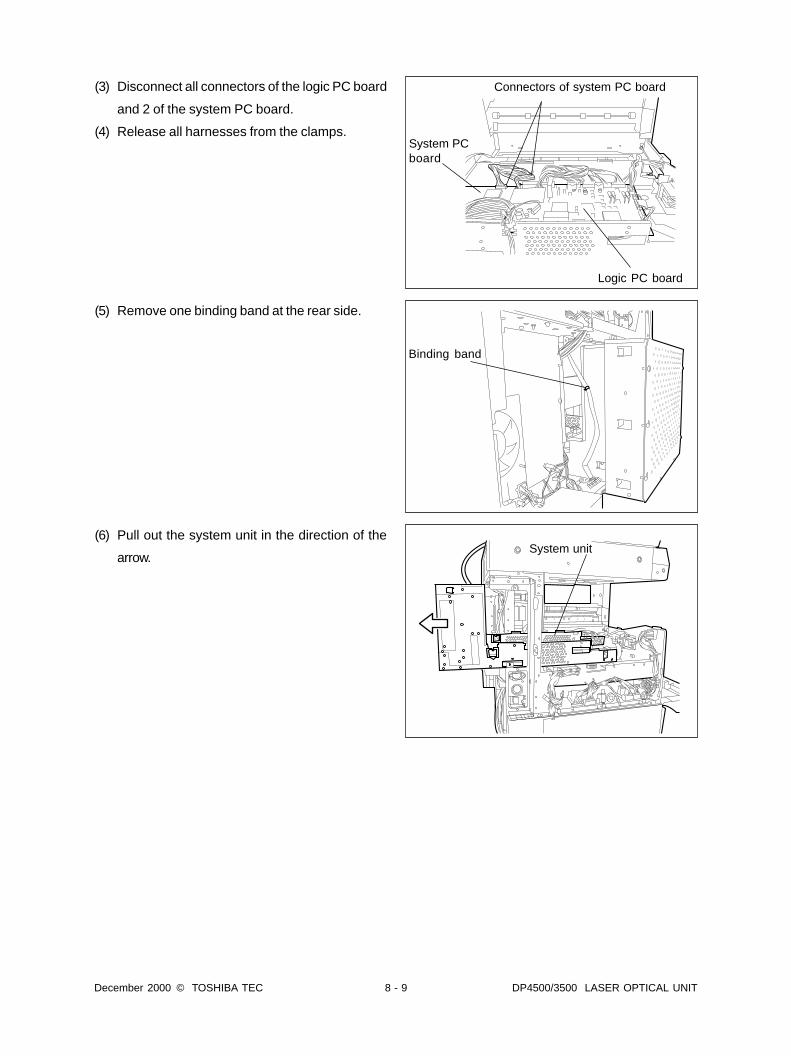
December 2000 © TOSHIBA TEC 8 - 9 DP4500/3500 LASER OPTICAL UNIT
(3) Disconnect all connectors of the logic PC board
and 2 of the system PC board.
(4) Release all harnesses from the clamps.
Logic PC board
System PCboard
Connectors of system PC board
(5) Remove one binding band at the rear side.
(6) Pull out the system unit in the direction of the
arrow.
Binding band
System unit

DP4500/3500 LASER OPTICAL UNIT 8 - 10 December 2000 © TOSHIBA TEC
(7) Remove the 3 fixing screws of the laser optical
unit.
(8) Take out the laser optical unit.
Notes: 1. The laser optical unit should be placed with
the motor facing upwards and not
impressing any load on it.
2. Do not leave fingerprints or stains on the
slit glass.
3. The laser optical unit is a precise
apparatus.
Pay close attention not to make any impact
or vibration on it.
4. The laser optical unit is precisely adjusted
and very sensitive to dust and stains. Do
not disassemble the unit in the field.
[Fixing screws of laser optical unit]

December 2000 © TOSHIBA TEC 9 - 1 DP4500/3500 PAPER FEEDING SYSTEM
9 PAPER FEEDING SYSTEM
9.1 FunctionsThe purpose of this system is to pick up paper from the cassette or bypass tray and send it to the transfer
section.
The paper feeding system mainly consists of the pickup roller, feed roller, separation roller, transport roller,
registration roller, bypass paper sensor, paper-empty sensor, paper-stock senser, feed sensor, registration
sensor and the drive system for these components.
(1) Pickup roller
This roller moves up and down to draw out a sheet of paper from the bypass tray or the cassette and
send it to the feed roller.
(2) Feed roller
This roller is mounted against the separation roller. It transports the paper from the pickup roller to the
registration roller.
(3) Separation roller
This roller is mounted against the feed roller. When two sheets of paper or more are sent from the
pickup roller, the load of the torque limiter of the separation roller is greater than the frictional force
between the sheets. As the result, the separation roller is stopped and the lower sheet of paper is not
advanced any further. When only one sheet of paper is sent from the pickup roller, the separation roller
is forced to rotate following the feed roller.
(4) Separation pad
This pad is mounted against the bypass feed roller. When two sheets of paper or more are sent from
the bypass pickup roller, the friction between the separation pad and the paper is greater than that
between the sheets. Therefore, the sheet(s) other than the paper at the top is(are) not transported any
further. When only one sheet is sent from the bypass pickup roller, the paper is transported forward due
to the friction between it and the bypass feed roller.
(5) Transport roller
This roller transports the paper sent from the feed roller to the registration rollers.
(6) Registration roller
Paper sent from the feed roller is pushed against the registration rollers, which align its leading edge.
The registration rollers then rotate to transport the paper to the transfer section.

DP4500/3500 PAPER FEEDING SYSTEM 9 - 2 December 2000 © TOSHIBA TEC
The following is the sensors which detect the presence/absence of paper and the position of the paper
being transported, to control the ON/OFF of the rollers.
(7) Bypass paper sensor
This sensor detects if paper is set in the bypass tray. If it is, bypass feeding is performed in preference
to cassette feeding.
(8) Paper-empty sensor
This is a emission type sensor and detects the presence/absence of paper in the cassette using an
actuator. When there is no paper in the cassette, the actuator blocks the light path of the sensor, and
the sensor determines that there is no paper.
(9) Paper-stock sensor
This is a emission type sensor which detects the amount of paper remaining in the cassette using an
actuator. When the remaining paper is almost finished and has become around 100 sheets, the actua-
tor blocks the light path of the sensor to notify that the paper quantity is getting less.
(10) Feed sensor
This sensor detects if the leading edge or trailing edge of the paper passed the feed roller. It also
detects jams such as paper misfeeding.
(11) Registration sensor
This sensor detects that the leading edge of the paper has reached the registration roller and the trailing
edge of the paper has passed the registration roller.

December 2000 © TOSHIBA TEC 9 - 3 DP4500/3500 PAPER FEEDING SYSTEM
Sectional view of paper feeding section (Front side)
No. Name
1 Bypass separation pad
2 Bypass feed roller
3 Bypass pickup roller
4 Upper cassette separation roller
5 Upper cassette feed roller
6 Upper cassette pickup roller
7 Transport roller
8 Lower cassette separation roller
No. Name
9 Lower cassette feed roller
10 Lower cassette pickup roller
11 Bypass paper sensor
12 Registration sensor
13 Registration roller (rubber roller)
14 Registration roller (metal roller)
15 Upper feed sensor
16 Lower feed sensor
2 311
13
4
14
1
6
7
8
10
12
15
5
9
16

DP4500/3500 PAPER FEEDING SYSTEM 9 - 4 December 2000 © TOSHIBA TEC
Paper feeding section drive system (Rear side)
No. Name
17 Bypass feed clutch
18 Transport clutch (low speed)
19 Transport feed clutch (high speed)
20 Upper cassette feed clutch
21 Lower cassette feed clutch
(G20/G25)(Clutch/G28)
(Clutch/G28)
(Clutch/G28)
(Clutch/G28)
(Clutch/G35)
17
18
19
21
20
(G27/G18)
(G24/G30)
(G40/G34)
(G31/G38)
(G35)
(G34)
(G35)
(G33)
(G33)
(G27/G21)
(G23)(G21)

December 2000 © TOSHIBA TEC 9 - 5 DP4500/3500 PAPER FEEDING SYSTEM
9.2 Description of Operations9.2.1 Operation of bypass pickup roller
When driving force is applied to the feed roller, the rotational force is transmitted to the pickup lever via the
spring clutch, and the pickup arm falls by its own weight. At this time, the pickup lever is stopped when the
spring clutch contacts with the stopper.
When the driving force is removed from the feed roller, the pickup lever and pickup arm are lifted up by the
force of the lever spring.
9.2.2 Operation of cassette pickup roller
When the cassette is inserted, the protrusion at the rear side of the cassette turns the lever (a) up in the
direction of the arrow A. The pickup roller and roller holder are then lowered by the spring (b).
Spring clutch
Feed roller
Lever spring
Pickup arm
Pickup roller
Pickup lever
Insertion direction
Lever (a)
Pickup roller
Spring (b)
Roller holderA

DP4500/3500 PAPER FEEDING SYSTEM 9 - 6 December 2000 © TOSHIBA TEC
9.2.3 Separation of paper
This model is equipped with a separation roller which
works to prevent multiple paper feeding. The sepa-
ration roller unit consists of the feed roller, separa-
tion roller, spring joint, etc., as shown in the right
figure.
The feed roller is rotated by the feed clutch in the
direction of the arrow ( ) at the same timing as
the pickup roller rotation.
The figure at lower right shows how duplicate feed-
ing is prevented: Since the friction between two
sheets is small, the lower sheet is stopped by the
separation roller and is not transported any further
while the upper sheet is transported by the feed roller
in the direction of the arrow ( ).
[Example]
When only one sheet enters between the rollers:
Since the transporting force of the feed roller is
greater than the braking force of the separation roller,
the separation roller is forced to rotate following the
feed roller, making the sheet go forward to the regis-
tration roller.
When two sheets enter between the rollers at the
same time:
Since the transporting force of the feed roller and
the breaking force of the separation roller are greater
than the frictional force between two sheets, the pa-
per A is transported in the direction of the arrow
( ) and the paper B is braked by the separation
roller and is not transported any further.
Feed roller
Separation roller
Spring joint
Feed roller
Separation roller
A
B

December 2000 © TOSHIBA TEC 9 - 7 DP4500/3500 PAPER FEEDING SYSTEM
9.2.4 General operation
[A] From power ON to standby status
(1) When the copier is turned ON, the tray-up motor starts to rotate forward and the upper cassette tray
starts to rise. When the tray-up sensor is turned ON (L n H), the tray-up motor is turned OFF causing
the tray to stop. At this time, if the empty sensor is OFF (L), it is judged that there is no paper in the
cassette. If the empty sensor is ON (H), there is paper in the cassette. The tray stops at raised position
regardless of the presence/absence of paper. The tray-up motor then starts to rotate in reverse and the
lower cassette tray starts to rise. The lower cassette tray is stopped in the same manner as the upper
cassette tray, and the empty sensor detects if there is paper in the cassette.
(2) If the cassette is not completely inserted when the copier is turned ON, the tray in that cassette does
not rise. When the cassette is inserted completely, the tray is raised and checks the presence/absence
of paper.
(3) If either of the feed sensors is ON (meaning there is paper on the transport path) when the copier is
turned ON, it is determined that a paper jam has occurred and no operation is enabled until the jammed
paper is removed.
[B] Standby status
(1) After the tray is moved up to check the presence/absence of paper as described above, the copier
enters the standby state. In the standby mode, the tray remains at the raised position.
(2) When a cassette is inserted or removed in the standby state, the tray is raised again and checks the
presence/absence of paper.
[C] Bypass feeding
• The bypass paper sensor detects paper in the bypass tray.
• The bypass feed clutch is turned ON, and then the bypass pickup roller and bypass feed roller are
rotated.
• The bypass pickup roller is lowered to start feeding the paper.
• The leading edge of the paper turns the registration sensor ON and the paper is aligned by the
registration rollers.
• The bypass feed clutch is turned OFF, causing the bypass pickup roller and bypass feed roller to
stop rotating. The bypass pickup roller moves up.
• The registration clutch is turned ON, and the paper is transported to the transfer section.

DP4500/3500 PAPER FEEDING SYSTEM 9 - 8 December 2000 © TOSHIBA TEC
[D] Cassette feeding
(D-1) Lower cassette
• The feed clutch and transport clutch (high speed) are turned ON, and the pickup roller, feed roller
and the transport roller are rotated to start feeding paper.
• The leading edge of paper turns ON the lower feed sensor. The feed clutch and transport clutch
(high speed) are then turned OFF and back ON.
• The leading edge of the paper turns ON the registration sensor and the paper is aligned by the
registration rollers.
• The feed clutch and transport clutch (high speed) are turned OFF causing the pickup roller, feed
roller and transport roller to stop rotating.
• The registration clutch and transport clutch (low speed) are turned ON, and the paper is trans-
ported to the transfer section.
(D-2) Upper cassette
• The feed clutch is turned ON and the pickup roller and feed roller start to rotate to start feeding the
paper.
• The leading edge of paper turns ON the registration sensor, and the paper is aligned by the regis-
tration rollers.
• The feed clutch is turned OFF causing the pickup roller and feed roller to stop rotating.
• The registration clutch is turned ON, and the paper is transported to the transfer section.

December 2000 © TOSHIBA TEC 9 - 9 DP4500/3500 PAPER FEEDING SYSTEM
1 2 3 4 5 6 7
IN1 IN2 M(+) GND M(–) N.C. VCC
9.3 Drive Circuit of Tray-up MotorTray-up motor (T-UP-MTR) : Driven by IC44 (upper/lower cassettes) (LGC: TA8428)
Block diagram of TA8428
IN1 and IN2 are input terminals to receive the signals from the microcomputer. The control logic, based on
the signals from the microcomputer, controls the rotation direction and ON/OFF of the motor.
Input Output
IN1 IN2 M (+) M (–)Remarks
H H L L BRAKE
L H L H CCW (upward)
H L H L CW (downward)
L L OFF (high impedance) STOP
Control logic
Thermal shut-down over-current protec-tion circuit
(Not used)

DP4500/3500 PAPER FEEDING SYSTEM 9 - 10 December 2000 © TOSHIBA TEC
9.4 Disassembly and Replacement[A] Bypass feed unit
(A-1) Bypass feed unit
(1) Remove the feed side rear hinge cover.
(2) Disconnect one connector and release the har-
ness from the clamp.
(3) Remove 2 screws. Release 2 hooks while the
bypass feed unit is lifted up, then take it off to-
ward you.
(A-2) Paper size detection board
(1) Release the harnesses from 3 clamps and dis-
connect one connector.
(2) Remove 2 screws and take off the hinge unit.
(3) Detach the bypass tray from the protrusion at
the fulcrum of the frame.
Clamp
Fulcrum
Bypass tray
Hinge unit
Connector
Clamp
Connector
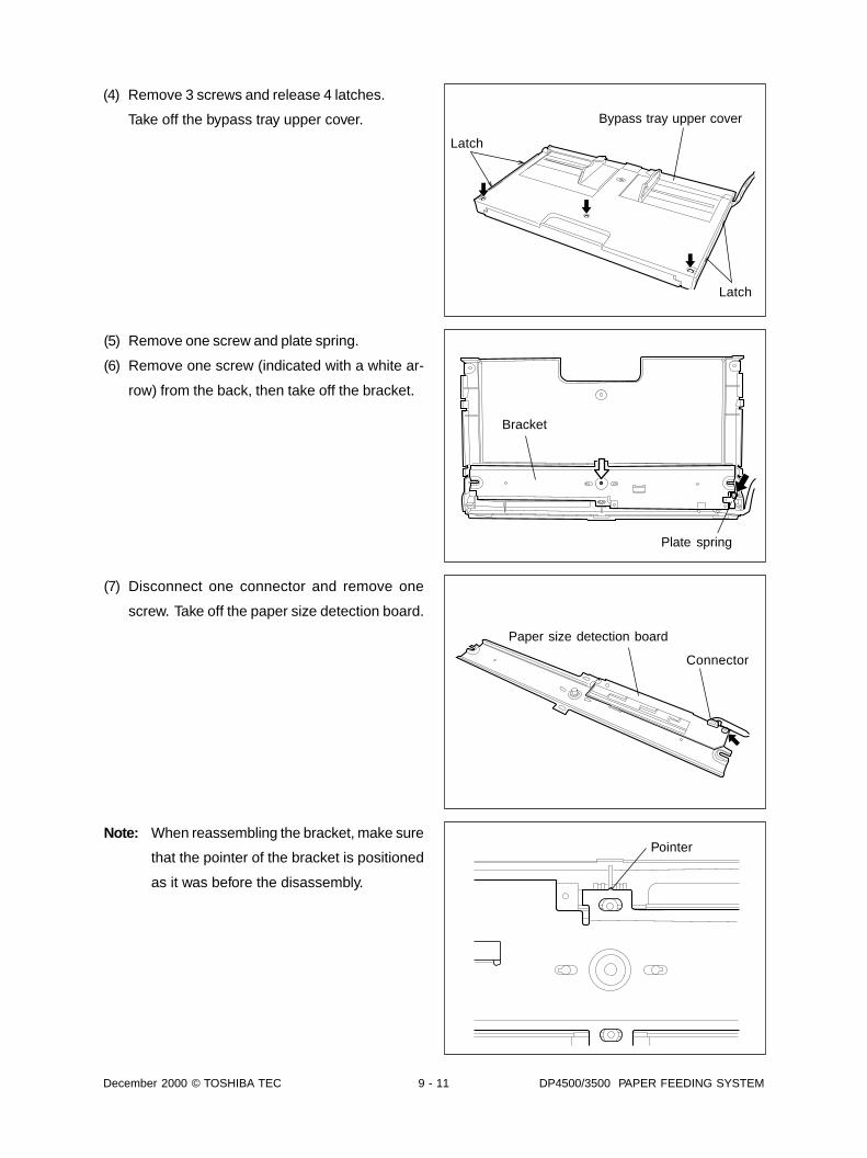
December 2000 © TOSHIBA TEC 9 - 11 DP4500/3500 PAPER FEEDING SYSTEM
(4) Remove 3 screws and release 4 latches.
Take off the bypass tray upper cover.
(5) Remove one screw and plate spring.
(6) Remove one screw (indicated with a white ar-
row) from the back, then take off the bracket.
(7) Disconnect one connector and remove one
screw. Take off the paper size detection board.
Note: When reassembling the bracket, make sure
that the pointer of the bracket is positioned
as it was before the disassembly.
Bypass tray upper cover
Latch
Latch
Bracket
Plate spring
Connector
Paper size detection board
Pointer

DP4500/3500 PAPER FEEDING SYSTEM 9 - 12 December 2000 © TOSHIBA TEC
(A-3) Separation pad
(1) Remove 4 screws and take off the bracket.
(2) Pull the separation pad in the direction of the
arrow to remove it from the bracket.
Detach the spring and then take off the pad.
(A-4) Bypass feed roller
(1) Remove one screw and take off the front side
paper guide.
(2) Remove one clip and take off the bypass feed
roller together with the one-way clutch.
(A-5) Bypass pickup roller
(1) Remove 2 screws and take off the bypass feed
cover.
Bracket
Separation pad
Spring
Bypass feed cover
Bypass feed roller
One-way clutch
Clip
Front side paper guide
(A-5)
(A-5)
(A-4)
(2) Remove one clip and pull out the shaft in the
direction of the arrow. Detach the timing belt,
and take off the bypass pickup roller.
Shaft
Clip
Timing belt
Bypass pickup roller

December 2000 © TOSHIBA TEC 9 - 13 DP4500/3500 PAPER FEEDING SYSTEM
Notes: Pay attention to the following when assem-
bling the bypass feed roller and pickup roller.
1. Put the timing belt securely around the
pulley.
Make sure that the belt is also put on the
belt tensioner.
2. Put the timing belt on the bypass pickup
roller correctly.
3. Attach the clip in the groove on the shaft
securely.
4. Make sure that there is no dirt or oil stain-
ing on the surface of the timing belt, pul-
ley and rollers.
5. Pay attention to the direction of the by-
pass pickup roller and feed roller when
they are installed.
(A-6) Bypass paper sensor
(1) Release the harness from the 2 clamps. Re-
move one screw and take off the sensor bracket.
(2) Disconnect the connector. Release the latches
and take off the bypass paper sensor.
Feedingdirection
Pickup roller
Feed roller
Separation pad
ConnectorBypass paper sensorClamp

DP4500/3500 PAPER FEEDING SYSTEM 9 - 14 December 2000 © TOSHIBA TEC
(A-7) Bypass feed clutch
(1) Release the harness from the 2 clamps and dis-
connect the connector. Remove the E-ring.
(2) Remove 4 screws. Take off the bypass feed roller
unit sliding it in the direction of the arrow.
(3) Remove one E-ring and loosen one setscrew.
Take off the bypass feed clutch.
Note: When assembling the bypass feed clutch,
push it against one end (feed roller unit side)
of the groove on the shaft.
Setscrew Feed clutch
ConnectorClamp
E-ring
Bypass feed roller unit
Groove
E-ring

December 2000 © TOSHIBA TEC 9 - 15 DP4500/3500 PAPER FEEDING SYSTEM
[B] Lower feed sensor
(1) Remove the feed side lower cover.
(2) Open the jam access cover, and take out the
transfer/separation charger. ( Chapter 11.5)
(3) Disconnect 3 connectors.
(4) Disconnect the fan connector of the front side
while the jam access cover unit is lifted up and
moved slightly in the direction of the arrow, then
take off the jam access cover unit.
(5) Remove one screw and take off the terminal
cover, then disconnect the connector.
(6) Remove 3 screws. Slide the transport guide unit
to the rear side and take it off from the front
side.
Transport guide unit
Terminal cover
Connector
Fan connector
Connector
Note: Make sure that the harnesses are securely
caught under the hooks when the connec-
tors of the transfer/separation charger are
connected.
Hook Black
Red
Red(in a black tube)

DP4500/3500 PAPER FEEDING SYSTEM 9 - 16 December 2000 © TOSHIBA TEC
[C] Registration sensor and upper feed sensor
(1) Remove the front side right cover.
(2) Release the latch from the shaft, and take off
the jam release knob.
(3) Disconnect one connector, remove one clamp
and 2 screws. Take out the pre-registration guide
from the front side.
(4) Remove one screw and take off the registration
sensor with the bracket attached.
(5) Disconnect the connector. Release the latches
and remove the registration sensor.
(6) Disconnect the connector. Release the latches
and remove the upper feed sensor.
Note: Do not damage or deform the roller rests
when installing/removing the pre-registration
guide.
Front side right cover Jam release knob
ConnectorPre-registration guide
Bracket
Registrationsensor
Upper feed sensor
(7) Disconnect the connector. Release the latches
and remove the lower feed sensor.
Connector
Lower feed sensor
Clamp
Roller rest
Roller rest

December 2000 © TOSHIBA TEC 9 - 17 DP4500/3500 PAPER FEEDING SYSTEM
[D] Registration roller
(1) Disconnect one connector and loosen one set-
screw.
Remove the rear side registration clutch.
( Chapter 10.4)
(2) Remove the cleaner unit. ( Chapter 11.5)
(3) Remove the E-rings from the front and rear sides
(one each). Slide the registration roller (rubber
roller) to the rear side and take it off from the
front side.
(4) Remove the E-rings and detach the springs from
the front and rear sides (one each). Take off the
registration roller (metal roller).
[E] Tray drive unit
(1) Remove 6 screws and disconnect one connec-
tor. Take off the tray drive unit with the metal
sheet attached.
(2) Remove 4 screws and take the tray drive unit
apart from the metal sheet.
(3) Turn the tray drive unit. Release 6 latches and
remove the cover.
Note: When removing the cover, be careful of the
spring inside the tray drive unit pushing the
cover.
[Front side]
[Rear side](3) E-ring
Connector
Latch
Latch
Registration roller
(4) Spring
(4) E-ring
(4) Spring
(4) E-ring
(3) E-ring
Cover
(1) (1)
(1)
(2)
(1)
(2)(1)
(2)
(2)
(1)

DP4500/3500 PAPER FEEDING SYSTEM 9 - 18 December 2000 © TOSHIBA TEC
(4) Remove the tray-up motor.
Note: When assembling the tray drive unit, match
the gear bosses with the holes of the cover.
[F] Transport clutch
(1) Remove one E-ring and 3 screws.
Take off the metal cover of the transport clutch.
Note: Do not move the transport roller shaft when
attaching the metal sheet cover. Fix the
screws in the order of (a), (b)and (c). Open
the side cover and check if the transport roller
rotates smoothly after it was attached.
(2) Remove the gears, disconnect the connectors
and loosen the setscrews.
Remove the transport clutches.
Notes: 1. Remember that the upper and lower
clutches are different in the diameter of
their shafts.
Upper clutch: 8mm
Lower clutch: 6mm
2. Attach the clutches to the shafts refer-
ring to the figure on the lower right.
[G] Cassette detection switch
(1) Pull out the cassette.
(2) Disconnect the connector. Release the latches
and remove the cassette detection switch from
the front side.
Gear Connector
Boss
Tray-up motor
Cassettedetectionswitch
E-ring
Clutch
Shaft0~0.5mm
(c)
(b)
(a)
Transport roller shaft
Metal sheetcover

December 2000 © TOSHIBA TEC 9 - 19 DP4500/3500 PAPER FEEDING SYSTEM
[H] Cassette feeding unit
(H-1) Cassette feeding unit
(1) Remove the cassette.
(2) Remove one screw and take off the cassette
feeding unit sliding it to the front side.
Cassette feeding unit
(H-2) Tray-up sensor
(1) Disconnect the connector. Release the latches
and remove the tray-up sensor.
(H-3) Paper-empty
(1) Disconnect the connector. Release the latches
and remove the paper-empty sensor.
(H-4) Paper-stock sensor
(1) Disconnect the connector. Release the latches
and remove the paper-stock sensor.
(H-5) Separation roller
(1) Remove one screw and take out the separation
roller holder.
(2) Remove the lever from the holder.
Take off the separation roller together with the
shaft.
(3) Remove the cover, arbor and clutch spring from
the shaft. Take off the separation roller.
Separation roller Feed clutch
Paper-empty sensorTray-up sensorPickup roller
Feed rollerPaper-stocksensor
[Separation roller]
Holder
Cover
Clutch spring
Separation roller
Shaft
Arbor
Spring
Lever
Arbor
Spring
(H-6) Feed roller
(1) Remove the clip and take off the feed roller.
Notes: 1. The feed roller and pickup roller are the same component parts.
2. There is a spring clutch inside the feed roller. Remove the feed roller together with the gear.
(H-7) Pickup roller
(1) Remove the clip and take off the pickup roller.
Note: There is a spring clutch inside the pickup roller. Remove the pickup roller together with the gear.

DP4500/3500 PAPER FEEDING SYSTEM 9 - 20 December 2000 © TOSHIBA TEC
(H-8) Feed clutch
(1) Disconnect one connector, detach one spring,
remove 2 screws and loosen one setscrew. Take
off the feed clutch.
Connector
Setscrew
Spring

December 2000 © TOSHIBA TEC 10 - 1 DP4500/3500 DRIVE SYSTEM
10. DRIVE SYSTEM
10.1 General DescriptionThe drive system drives the drum, developer unit, cleaner unit, fuser unit, transport roller, cassette feed
roller and registration roller.
The drive system is driven by the rotation of the main motor.
10.2 Functions• Drum drive ............................. Drives the drum by transmitting the rotation of the main motor through the
gears to the drum flange gear.
• Developer unit drive ............... Drives the developer unit by transmitting the rotation of the main motor
through the gears to the developer unit gears.
• Fuser unit drive ...................... Drives the fuser unit by transmitting the rotation of the main motor through
the gears to the fuser unit gears.
• Cleaner unit drive ................... Drives the cleaner unit gear by the rotation of the drum flange gear.
• Registration roller drive .......... Drives the registration rollers by transmitting the rotation of the main motor
through the gears and clutches.
• Transport roller drive .............. Drives the transport roller by transmitting the rotation of the main motor
through the gears and clutches.
• Cassette feed roller drive ....... Drives the cassette feed roller by transmitting the rotation of the main
motor through the gears and clutches.
Main motor
Developerunit drive gear
(G36/G21)
Feeding systemdrive gear
Cleaner unitdrive gear
(G22)
Registration rollerdrive unit
(G50/G27)
(G72/G30)
(G25/G14)
(G27)
(G23)
(G24)(G23)
(G47)
(G25)
(G33)
(G24)
Fuser unitdrive gear
(G64/G30)(G28/G25)
(G10)

DP4500/3500 DRIVE SYSTEM 10 - 2 December 2000 © TOSHIBA TEC
+(MAMCK)
MAMPL
MAMCW
MAMBK
MAMON
10.3 Main Motor10.3.1 Main motor drive
Difference
Speedcomparator
Rotationcontrol
Voltagedetectioncircuit
Excitationphaseswitchingsection
Rotorpositiondetection
Phasecomparator
Hall element A
FG pulse
Phase W
Phase V
Phase U
Main motor
Controlsignal
(1) LGC outputs the control signals for the the main motor rotation. (MAMCW: Motor rotation direction
setting, MAMON: Motor rotation command)
(2) The excitation phase switching section excites each phase of the main motor nnnnn The main motor is
rotated.
(3) Hall elements A, B and C detect the rotation position of the motor (rotor).
(4) The excitation phase switching section switches the excitation of each phase.
(By repeating (2) through (4), the motor keeps rotating.)
(5) An FG pulse is generated by the FG pattern of the encoder attached to the main motor.
(6) The FG pulse and the reference frequency from the LGC are compared in terms of the phase and
speed, and the difference is added to the IC1. The fluctuations in the power supply voltage is also
added to the value. (Signal generation)
(7) In accordance with the signal obtained in the step (6), the excitation phase switching section changes
the switching timing.
i.e. The FG pulse and reference frequency are controlled to be equal. nnnnn The main motor rotates at a
fixed speed. (Locked range)
(8) When the main motor enters the locked range, the excitation phase switching section outputs the
MAMPL signal to the LGC. (“L” level)
(9) When the MAMBK from the LGC becomes “L” level, the main motor is braked. When the MAMON signal
becomes “H” level, the main motor is stopped.
Hall element C
Wavecorrection
Photo-interruptor
Hallelement B
Reference frequency
Lockprotectioncircuit
Difference

December 2000 © TOSHIBA TEC 10 - 3 DP4500/3500 DRIVE SYSTEM
10.3.2 Control signals
(1) MAMCW signal (LGC nnnnn MTR: Input)
This is a signal to switch the direction of the main motor rotation. When this signal becomes “L” level,
the main motor rotates counterclockwise as seen from the rear side, and drives the developer unit,
drum, fuser roller, etc to the appropriate direction.
(2) MAMPL signal (MTR nnnnn LGC: Output)
When the difference of the FG pulse cycle against the reference frequency is within ±6.25%, it is
specified that the motor is in a lock range (normal rotation), and this MAMPL signal becomes “L” level.
At this time, the LED “D4” is lit.
(3) MAMCK signal (LGC nnnnn MTR: Input)
This is a reference clock signal to rotate the main motor at a fixed speed.
(4) MAMBK signal (LGC nnnnn MTR: Input)
This is a signal to stop the main motor.
When it becomes “L” level, the main motor is braked.
(5) MAMON signal (LGC nnnnn MTR: Input)
This is a signal to turn ON/OFF the main motor. When it becomes “L” level, the motor is rotated.
Signal level of the motor circuit
Signal Level “H” Level “L”
MAMCW CCW direction CW direction
MAMPL Abnormal rotation Normal rotation
MAMCK Reference clock
MAMBK Brake OFF Brake ON
MAMON Motor OFF Motor ON
* The signal names are for the connector J313(LGC).

DP4500/3500 DRIVE SYSTEM 10 - 4 December 2000 © TOSHIBA TEC
(3) Turn over the gear unit and remove 2 screws to
unfix 2 terminals.
Note: Do not bend the plate spring attached to the
terminal when installing or removing the gear
unit.
(4) Remove one screw and disconnect one connec-
tor. Take off the toner bag full detection sensor
with the bracket attached.
(5) Remove the E-rings and take off the gears.
Note: When assembling the gear unit, set the gears
referring to the figure in the page 10-1, and
pay attention to the position of each gear.
10.4 Disassembly and Repalacement[A] Main motor
(1) Take off the rear side upper/lower covers.
(2) Take off the developer unit cooling fan unit
( Chapter 11.5)
(3) Disconnect one connector, remove 2 screws and
release one lock support. Take off the main mo-
tor with the board attached.
[B] Registration clutch
(1) Disconnect one connector and remove one set-
screw. Take off the registration clutch.
[C] Gear unit
(1) Remove 5 screws and disconnect 3 connectors.
(2) Take off the gear unit while the arm is held up.
ConnectorRegistration clutch
Main motor
Set-screw
Connector
Connector Arm
Locksupport
Plate spring
Connectors
Toner bag fulldetectionsensor
(3)(3)
(4)

December 2000 © TOSHIBA TEC 10 - 5 DP4500/3500 DRIVE SYSTEM
[D] Drum drive gear
Note: Do not loosen or remove the 3 red screws
fixing the bracket of the drum drive gear.
Bracket
Drum drive gear

DP4500/3500 DRIVE SYSTEM 10 - 6 December 2000 © TOSHIBA TEC

December 2000 © TOSHIBA TEC 11 - 1 DP4500/3500 DRUM AREA
11. DRUM AREA
11.1 ConfigurationThe parts and units located around the drum and the drum itself are described in this section.
This area mainly consists of the following.
• Cleaner unit Drum
Main charger
Cleaner Cleaning blade
Toner recovery blade
Toner recovery auger
• Transfer / separation charger
• Sub-separation fan / Exhaust fan
• Discharge lamp
• Toner bag / Toner bag full detection sensor
• Developer unit cooling fan / Middle cooling fan
• Drum thermistor
[Sectional view of drum area]
Discharge lamp
Middle cooling fan
Toner recovery auger
Drum
Cleaning bladeSub-separationfan
Exhaust fan
Separationcharger
Toner recovery blade
Transfer charger
Transfer guide
Main charger
Drum thermistor

DP4500/3500 DRUM AREA 11 - 2 December 2000 © TOSHIBA TEC
11.2 Functions(1) Drum
The drum is made of a cylindrical aluminum base coated with thin film of organic photoconductive
substance.
The photoconductive object becomes insulative (the electrical resistance is high) when it is not ex-
posed to the light and electrically conductive (the electrical resistance is low) when it is exposed to the
light. This object is called a photoconductor.
(2) Main charger
The main charger consists of a metal rod with U-shaped section, insulated blocks at both ends of the
rod and charger wire attached between them.
When a high voltage is applied to the charger wire, the air around it is charged (ionized). The ionized air
then flows into the drum causing it to be charged. This phenomenon is called “corona discharge”.
Negative charge caused by the corona discharge is applied to the drum surface evenly in dark place.
The main charger is equipped with a wire cleaner to clean the wire.
(3) Cleaner
(a) Cleaning blade
This blade is pressed against the drum surface with a constant force by the pressure springs, and
scrapes off the residual toner from the drum surface.
(b) Recovery blade
This blade catches the toner scraped off by the cleaning blade.
(c) Toner recovery auger
This auger carries the residual toner scraped off to the toner bag.
(4) Transfer/separation charger
(a) Transfer guide
This guide guides the paper transported from the feeding unit to the transfer section.
Positive (+) bias voltage is applied to the guide to prevent the transferability being lowered under
conditions such as high humidity.
(b) Transfer charger
The transfer charger applies a charge (= positive charge) which is contrary to the charging polarity
of the toner to the back of the paper. The toner image is transferred electrostatically on paper by
performing this corona discharge.

December 2000 © TOSHIBA TEC 11 - 3 DP4500/3500 DRUM AREA
(c) Separation charger
After the transfer process, the corona discharge applies a bipolar charge (AC) on the back of the
paper to separate the paper adhering to the drum surface.
(5) Sub-separation fan
This fan works to help the separation of paper from the drum surface by sucking the air from the back
of the paper.
(6) Discharge lamp
Discharging is a process to decrease or eliminate the static electricity on the drum surface.
The electrical resistance of the photosensitive layer is decreased by the light irradiation, and the
residual charge on the drum surface is neutralized and eliminated (cleaned). The electrical potential of
the drum surface is fixed to a certain amount before the drum is charged (The pre-exposure effect).
(7) Toner bag
The residual toner scraped off the drum surface by the cleaning blade is disposed in this bag.
(8) Toner bag full detection sensor
When the toner bag is full of used toner, the toner recovery auger in the cleaner is pushed back by the
toner and blocks the light emission of this sensor, as the result, notifying that the toner bag is full.

DP4500/3500 DRUM AREA 11 - 4 December 2000 © TOSHIBA TEC
PWA-F-LGC-320 PS-HVT-320
IC2
IC13 IC10IC31
BC-RAM Vc
11.3 Output Control Circuits of High-Voltage Transformer11.3.1 Overview
• Generate the output control voltage Vc of the main charger, transfer/separation charger, transfer guide
bias and developer bias.
• Convert Vc n n n n n The current is output linearly.
11.3.2 Description of operations
• Outputs the adjustment value of the main, transfer and separation chargers and developer bias in the
BC-RAM to the main CPU.
x
• Outputs the control voltage data from the main CPU to the D/A converter.
x
• Converts to the analog data by the D/A converter.
x
• Outputs the control voltage Vc to the main, transfer and separation chargers, transfer guide bias and
developer bias transformer.
x
• The main, transfer and separation chargers, transfer guide bias and developer bias transformer generate
output current or voltage which is proportional to the control voltage Vc.
* Adjustment of the control voltage Vc (change of adjustment data) is performed in the adjustment mode.
* The output value of the transfer guide bias is fixed when the high-voltage transformer is shipped from
the factory.
MainCPU
D/Aconverter Output
AnalogDigitaldata
Main/transfer/separation/chargers,developerbias andtransferguide bias
Gatearray
Adjustmentvalue

December 2000 © TOSHIBA TEC 11 - 5 DP4500/3500 DRUM AREA
J311-14 HVSAV
J311-17 HVTVR
J311-19 HVDVR
J311-21 HVMVR
MAINCPU
BC-RAM
IC13
IC10IC31
IC2
Gatearray
D/Aconverter
Separation charger
Developer bias
Transfer charger
Main charger

DP4500/3500 DRUM AREA 11 - 6 December 2000 © TOSHIBA TEC
11.4 Drum Temperature Detection Circuit(1) Purpose of the drum temperature detection circuit
The amount of charge on the drum surface varies greatly with the surface temperature of the drum. This
circuit detects the temperature of the drum surface, and the amount of charge on the drum surface is
controlled to be constant based on the result.
(2) Configuration of the drum temperature detection circuit
Drum temperature detection circuit
The voltage developed through R38, thermistor and R37 is input via an analog multiplexer (IC94) to the
microcomputer as a temperature signal.
TH
C47
GND GND
+5V
100
R158 DRMTH-1CPU
R37
R380

December 2000 © TOSHIBA TEC 11 - 7 DP4500/3500 DRUM AREA
11.5 Disassembly and Replacement[A] Cleaner unit
(1) Open the front cover and take out the toner bag
and developer unit. ( Chapter 12.5)
(2) Open the bypass feed unit, ADU and jam ac-
cess cover.
(3) Remove 2 screws and pull out the cleaner unit.
[B] Main charger
(B-1) Main charger
(1) Pull out the cleaner unit.
(2) Release the latches and pull out the main charger
in the direction of the arrow.
Note: Do not touch or damage the drum surface.
(B-2) Main charger grid
(1) Push the terminal head at the front side to
remove the grid.
Note: Do not touch the mesh pattern of the grid.
(B-3) Charger wire
* Length: 363mm, tungsten wire; diameter 0.06mm
(1) Remove the terminal covers of the front and rear
sides.
Cleaner unit Jam access cover
Developer unit
Latch
Grid
Push
Terminal cover
[Rear side] [Front side]

DP4500/3500 DRUM AREA 11 - 8 December 2000 © TOSHIBA TEC
(2) Remove the terminal, detach the spring and take
off the wire.
Notes: Be careful of the following when attaching
the wire.
1. Put the wire in the V-grooves of the front
and rear sides.
2. Do not twist the wire.
3. Do not touch the wire directly with your
bare hands.
(B-4) Wire cleaner
(1) Release the lock at the front side of the wire
cleaner.
(2) Turn the wire cleaner in the direction of the ar-
row, and pull out the cleaning pad unit from the
charger case window.
(3) Remove the cleaning pads.
Note: When attaching the wire cleaner, send the wire
cleaner to the rear side end and be sure that
the 2 cleaning pads do not touch the wire.
[Rear side] [Front side]
V-groove
Spring Terminal
Lock Charger case window
Cleaning padWire cleaner
Cleaning pad
[C] Drum
(1) Pull out the cleaner unit and remove the main
charger.
(2) Release the latch and take off the cleaner stay.
Cleaner stay
Latch

December 2000 © TOSHIBA TEC 11 - 9 DP4500/3500 DRUM AREA
[D] Cleaner
(D-1) Cleaning blade
(1) Pull out the cleaner unit. Remove the main
charger and the drum.
(2) Remove 2 screws.
Note: Do not touch or damage the edge of the clean-
ing blade.
(D-2) Recovery blade
(1) Remove the recovery blade.
Notes: 1. When attaching the recovery blade, clean
the frame of the cleaner side and make
sure not to deform the blade.
2. Attach the recovery blade while it is
pushed against the part with a difference
in level on the surface of the frame.
3. Press the part sticking to the cleaner with
the double-sided adhesive tape to attach
the blade securely.
Cleaning blade
Recovery blade
(3) Turn the lever to the left to release the lock. Pull
out the drum shaft.
(4) Take off the drum upward.
Drum gear
Lever
Notes: 1. Release the pressure of the cleaning blade
using a jig before installing the drum.
2. Insert the jig into space made by pressing
the blade holder as shown in the right
figure.
3. Do not touch or damage the edge of the
cleaning blade.
Space to insert the jig

DP4500/3500 DRUM AREA 11 - 10 December 2000 © TOSHIBA TEC
(D-3) Separation finger
(1) Remove 3 separation fingers.
Notes: 1. Remove the drum before replacing the
separation fingers to prevent damaging
the drum surface.
2. After the separation fingers are replaced,
check if the pressurization of them is nor-
mal using your finger.
Separation finger
(E-2) Charger wires
* Length: 353mm
2 tungsten wires: diameter 0.06mm
(The transfer charger wire and separation charger
wire are the same component parts.)
(1) Remove the separation supporter.
(2) Remove the terminal covers of the front and rear
sides.
(3) Remove the terminals, detach the springs and
take off the wires.
Notes: Be careful of the following when attaching
the charger wires.
1. Put the wires in the V-grooves of the front
and rear sides.
2. Do not twist the wires.
3. Do not touch the wires directly with your
bare hands.
Terminal cover
Separation supporter
[Rear side][Front side]Spring
TerminalV-groove V-groove
[E] Transfer/separation charger
(E-1) Transfer/separation charger
(1) Open the bypass feed unit, ADU and jam ac-
cess cover.
(2) Release the latches and remove the transfer/
separation charger.
Note: Do not deform the plate spring when the
charger is attached.
Latch
Platespring

December 2000 © TOSHIBA TEC 11 - 11 DP4500/3500 DRUM AREA
[F] Exhaust fan and sub-separation fan
(1) Open the jam access cover.
(2) Take off the transfer/separation charger.
(3) Remove 2 screws and take off the fan cover.
Fan cover
[G] Middle cooling fan
(1) Open the front cover. Take out the toner bag,
toner cartridge, developer unit and cleaner unit.
(2) Take off the paper receiving tray and tray back
cover.
(3) Remove 4 screws and disconnect one connec-
tor. Take off the bracket and cover plate of the
toner cartridge drive unit.
(4) Remove 3 screws and 3 washers.
Disconnect 2 connectors and take off the
exhaust fan and sub-separation fan.
Note: Pay attention to the direction of the air flow
when attaching the fan.FLO
W
FLOW
Sub-separation fan Exhaust fan
[Rear side]
[Front side]
Cover plate
Connector
BracketCover plate

DP4500/3500 DRUM AREA 11 - 12 December 2000 © TOSHIBA TEC
(4) Remove 2 screws and take off the toner bag
holder.
Toner bag holder
(5) Take off the rear side upper and lower covers.
(6) Disconnect the developer bias connector of the
high-voltage transformer.
(7) Remove one screw and take off the developer
unit guide.
(8) Remove 2 screws and take out the middle cool-
ing fan duct.
Developer bias connector
Developer unit guide
Middle cooling fan duct
High-voltage transformer
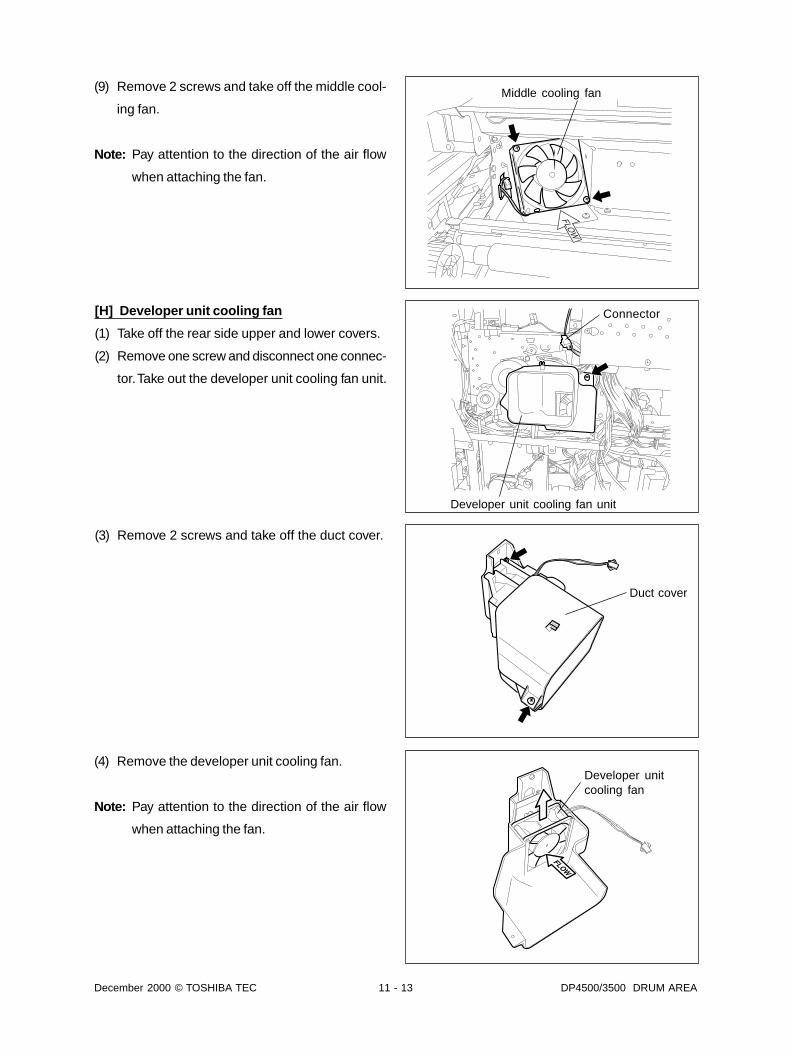
December 2000 © TOSHIBA TEC 11 - 13 DP4500/3500 DRUM AREA
(9) Remove 2 screws and take off the middle cool-
ing fan.
Note: Pay attention to the direction of the air flow
when attaching the fan.
Middle cooling fan
[H] Developer unit cooling fan
(1) Take off the rear side upper and lower covers.
(2) Remove one screw and disconnect one connec-
tor. Take out the developer unit cooling fan unit.
(3) Remove 2 screws and take off the duct cover.
(4) Remove the developer unit cooling fan.
Note: Pay attention to the direction of the air flow
when attaching the fan.
Developer unit cooling fan unit
Duct cover
Developer unitcooling fan
Connector

DP4500/3500 DRUM AREA 11 - 14 December 2000 © TOSHIBA TEC
[J] Toner bag full detection sensor
(1) Take off the rear side upper and lower covers.
(2) Take out the developer unit cooling fan unit.
(3) Take out the main motor, registration clutch and
gear unit.
( Chapter 10.4)
(4) Remove one screw and disconnect one connec-
tor. Take out the toner bag full detection sensor
with the bracket attached.
(3) Remove the discharge lamp.
Discharge lamp
(5) Disconnect one connector. Release the latches
and take out the toner bag full detection sensor.
Toner bag fulldetection sensorConnector
Toner bag full detection sensor
Latch
[I] Discharge lamp
(1) Take out the developer unit and cleaner unit.
(2) Remove one screw and disconnect one connec-
tor. Take out the discharge lamp unit.
Connector
Connector

December 2000 © TOSHIBA TEC 12 - 1 DP4500/3500 DEVELOPMENT SYSTEM
12. DEVELOPMENT SYSTEM
12.1 ConfigurationDevelopment system consists of the following unit and components.
• Toner cartridge/toner cartridge detection switch
• Humidity sensor
• Drive unit for toner cartridge
• Developer unit Developer material
Mixers -1 and -2
Developer sleeve (magnetic roller)
Doctor blade
Auto-toner sensor
Drum thermistor
Drum
Doctor bladeMixer-2
Developer sleeve
Mixer-1
Auto-toner sensor
[Sectional view of developer unit]
Drum thermistor
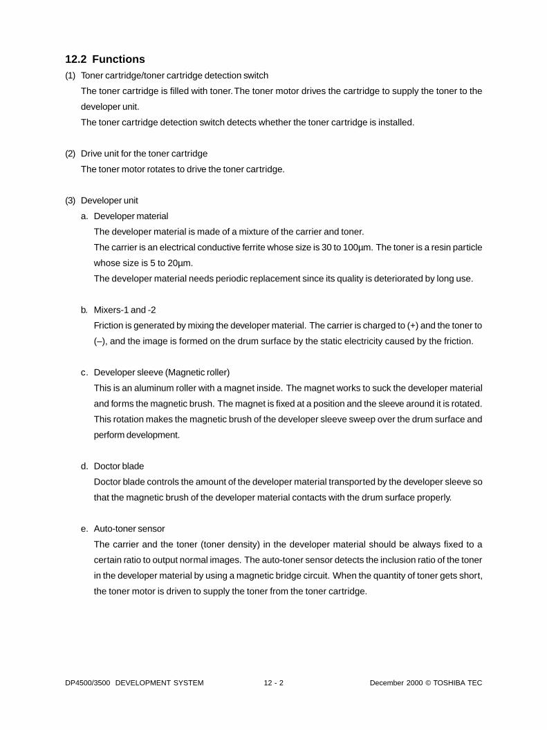
DP4500/3500 DEVELOPMENT SYSTEM 12 - 2 December 2000 © TOSHIBA TEC
12.2 Functions(1) Toner cartridge/toner cartridge detection switch
The toner cartridge is filled with toner. The toner motor drives the cartridge to supply the toner to the
developer unit.
The toner cartridge detection switch detects whether the toner cartridge is installed.
(2) Drive unit for the toner cartridge
The toner motor rotates to drive the toner cartridge.
(3) Developer unit
a. Developer material
The developer material is made of a mixture of the carrier and toner.
The carrier is an electrical conductive ferrite whose size is 30 to 100µm. The toner is a resin particle
whose size is 5 to 20µm.
The developer material needs periodic replacement since its quality is deteriorated by long use.
b. Mixers-1 and -2
Friction is generated by mixing the developer material. The carrier is charged to (+) and the toner to
(–), and the image is formed on the drum surface by the static electricity caused by the friction.
c. Developer sleeve (Magnetic roller)
This is an aluminum roller with a magnet inside. The magnet works to suck the developer material
and forms the magnetic brush. The magnet is fixed at a position and the sleeve around it is rotated.
This rotation makes the magnetic brush of the developer sleeve sweep over the drum surface and
perform development.
d. Doctor blade
Doctor blade controls the amount of the developer material transported by the developer sleeve so
that the magnetic brush of the developer material contacts with the drum surface properly.
e. Auto-toner sensor
The carrier and the toner (toner density) in the developer material should be always fixed to a
certain ratio to output normal images. The auto-toner sensor detects the inclusion ratio of the toner
in the developer material by using a magnetic bridge circuit. When the quantity of toner gets short,
the toner motor is driven to supply the toner from the toner cartridge.

December 2000 © TOSHIBA TEC 12 - 3 DP4500/3500 DEVELOPMENT SYSTEM
12.3 Drive Circuit of Toner MotorThe toner motor (brush motor) is a motor to supply toner to the developer unit.
The toner motor is driven by the transistor TA8428 (logic PC board: IC41).
Circuit diagram of the toner motor
Motor driver TA8428 (IC41) is connected with both ends of the motor wire.
— When the PD6(TNRMT-1A) of the G/A becomes “L” and PD7 (TNRMT-0A) becomes “H” levels, current
flows into the motor wire and the motor is rotated.
— When both of PD6 (TNRMT-1A) and PD7 (TNRMT-0A) of the G/A become “H” level, the motor is braked
and stopped.
— When both of PD6 (TNRMT-1A) and PD7 (TNRMT-0A) become “L” level, the motor waits for the next
command (the motor is stopped).
MAIN
-CPU
IC13
G/A
IC10
TD62385
IC28
TA8428
IC41
PD6 1
2
3
5
R344
PD7
Toner motor

DP4500/3500 DEVELOPMENT SYSTEM 12 - 4 December 2000 © TOSHIBA TEC
BC-RAMIC40
CPUIC10
GAIC30
PWA-SYS
PWA-LGC
CPUIC13
95C063F
GAIC10
LCA301IC31
MB88347
TA8428IC41
12.4 Auto-Toner Circuit12.4.1 General description
(1) Function of the auto-toner circuit
· Detects the toner density in the developer material, and supplies toner when the density is lowered to
a certain level.
· Detects that there is no toner left in the cartridge (toner-empty detection).
(2) The auto toner circuit consists of the following:
· Auto-toner sensor : Detects the toner density.
· Control section : Controls the toner density so that the toner in the developer material is fixed to
certain ratio.
· Toner motor : Supplies toner to the developer material.
· Display : Indicates toner-empty information.
Display panel
Toner cartridge
Toner Tonermotor
Auto-toner sensor
Developer material
Controlvoltage signal
Control panel
Developer unit
D/Aconverter
Arithmetic and control unit
MAIN

December 2000 © TOSHIBA TEC 12 - 5 DP4500/3500 DEVELOPMENT SYSTEM
12.4.2 Function of auto-toner sensor
(1) Function
a. Initialization adjustment function —At the first use of the copier or when the developer material is
replaced with a new one.
Automatically adjusts the output value of the auto-toner sensor responding to humidity (input value
to the main CPU) for the toner density of the new developer material so that it stays in range of 2.35
to 2.45V.
b. Stabilizing the toner density —During the copying operation
Maintains the toner density to a certain ratio as follows.
Toner is consumed.
nThe toner density is lowered.
nChange in the auto-toner sensor output responding to humidity is detected.
nThe toner motor is driven.
nToner is supplied from the toner cartridge to the developer unit.
c. Toner-empty detection and recovery:
Detects that there is no toner in the toner cartridge:
The toner motor is driven.
nThe auto-toner sensor output does not change.
nThe toner density does not change.
nIt is determined there is no toner in the cartridge (toner empty).
Recovering from the toner-empty state:
The toner motor is driven.
nToner is supplied.
nThe auto-toner sensor output changes.
nThe toner density returns to normal value.
nThe toner-empty state is cleared.

DP4500/3500 DEVELOPMENT SYSTEM 12 - 6 December 2000 © TOSHIBA TEC
(2) Function of auto-toner sensor
The auto-toner sensor consists of the following circuits:
· Drive winding : A magnetic head (primary side) with a high-frequency magnetic field, which
forms a magnetic circuit in the developer material.
· Detection winding : Receives the change in the magnetic resistance of the developer material
through the magnetic circuit (secondary side).
· DC conversion circuit : Converts a high-frequency output from the detection winding into a DC signal
(auto-toner output VATS
).
When the toner density is low—
The ratio of the toner against the carrier in the developer material decreases.
nThe magnetic resistance decreases.
nThe detection output increases.
nThe auto-toner output VATS
increases.
When the toner density is high—
The ratio of the toner against the carrier in the developer material increases.
nThe magnetic resistance increases.
nThe detection output decreases.
nThe auto-toner output VATS
decreases.
Magnetic resistance
Drivewinding
(Developer material)
Magnetic circuit
Detectionwinding
DCconversion
circuit
Auto-toneroutput
To the mainCPU (LGC)
VATS

December 2000 © TOSHIBA TEC 12 - 7 DP4500/3500 DEVELOPMENT SYSTEM
12.4.3 Adjustment using the humidity sensor
Variation in the output of the auto-toner sensor due to humidity is corrected using the humidity sensor to
maintain the toner density in the developer material at a certain amount. The feedback control function
using the humidity sensor is applicable to the main charger grid, developer bias and laser power as follows.
The feedback control function can be set in the setting mode [0] + [8].
: Function effective —: Function ineffective
Code setting
08/839=0 (default)
08/839=1
08/839=2
08/839=3
Control of the auto-toner outpout VATS
—
—
Control of the main charger grid,
developer bias and laser power
—
—

DP4500/3500 DEVELOPMENT SYSTEM 12 - 8 December 2000 © TOSHIBA TEC
12.5 Disassembly and Replacement[A] Developer unit
(1) Open the front cover and take out the toner bag.
(2) Loosen one blue screw and disconnect one con-
nector.
Take out the developer unit.
[B] Developer material
(B-1) Disposition of developer material
(1) Remove the top cover. (Release the protrusions
and latches, and slide the cover in the direction
of the arrow to take out the cover.)
(2) Incline the developer unit and remove the de-
veloper material from the part shown with the
arrow.
(B-2) Filling developer unit with developer mate-
rial
(1) Remove the lid of the developer bottle and fill
the developer unit with the developer material.
(2) Rotate the gear at the rear side manually in the
direction of the arrow to spread out the devel-
oper material over the developer sleeve.
Note: Securely attach 4 latches and 2 protrusionsat both sides of the cover when fixing thetop cover.
Connector
Latch
Protrusion
Protrusion
Top cover
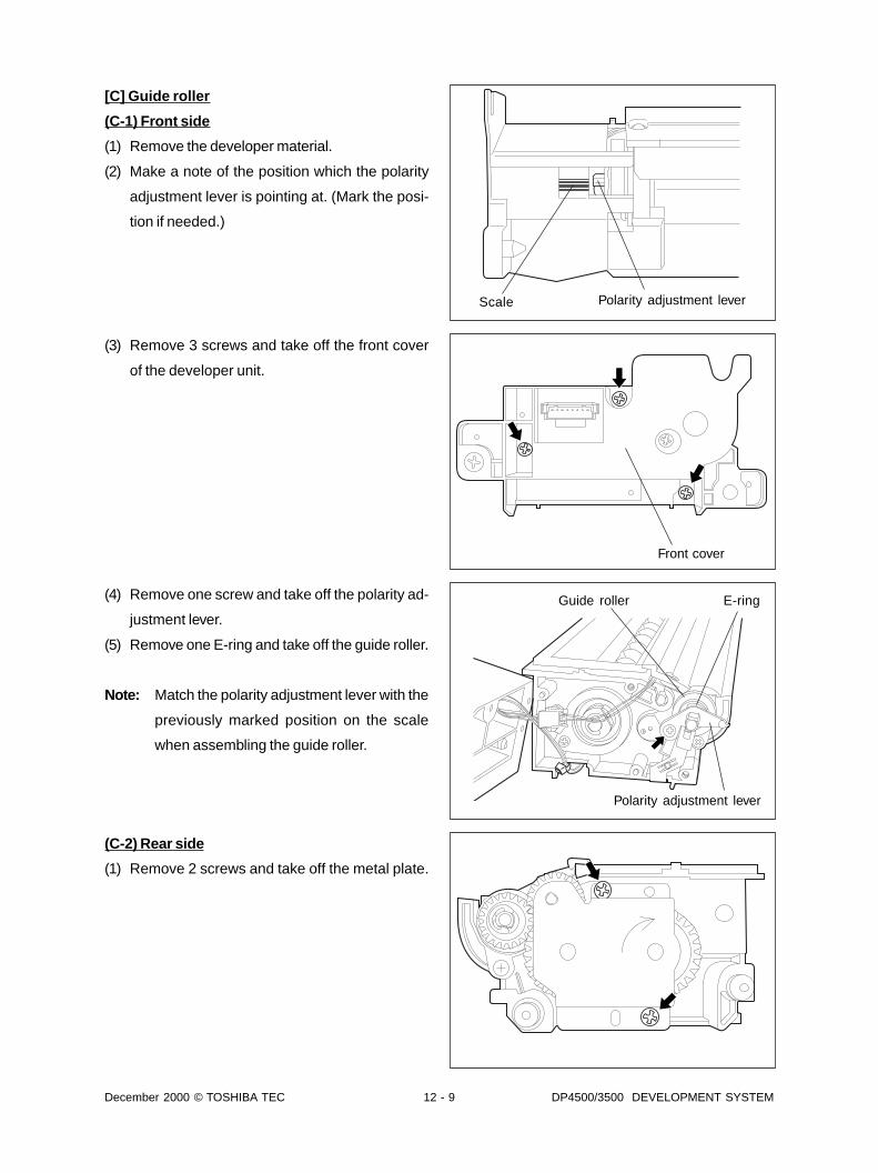
December 2000 © TOSHIBA TEC 12 - 9 DP4500/3500 DEVELOPMENT SYSTEM
[C] Guide roller
(C-1) Front side
(1) Remove the developer material.
(2) Make a note of the position which the polarity
adjustment lever is pointing at. (Mark the posi-
tion if needed.)
(3) Remove 3 screws and take off the front cover
of the developer unit.
(4) Remove one screw and take off the polarity ad-
justment lever.
(5) Remove one E-ring and take off the guide roller.
Note: Match the polarity adjustment lever with the
previously marked position on the scale
when assembling the guide roller.
(C-2) Rear side
(1) Remove 2 screws and take off the metal plate.
Scale Polarity adjustment lever
Front cover
Guide roller E-ring
Polarity adjustment lever

DP4500/3500 DEVELOPMENT SYSTEM 12 - 10 December 2000 © TOSHIBA TEC
(2) Remove one E-ring and 4 gears.
(3) Take off the guide roller.
[D] Auto-toner sensor
(1) Dispose of the developer material.
(2) Remove one screw and disconnect one connec-
tor. Take off the auto-toner sensor from the bot-
tom side of developer unit.
[E] Drum thermistor
(1) Take off the front cover of the developer unit.
(2) Remove 2 screws and take off the developer
sleeve cover.
(3) Remove one screw and disconnect one connec-
tor, and take off the drum thermistor.
Guide rollerGear
E-ring
Connector
Developer sleeve cover
Connector

December 2000 © TOSHIBA TEC 12 - 11 DP4500/3500 DEVELOPMENT SYSTEM
[F] Developer sleeve
(1) Dispose of the developer material.
(2) Take off the developer sleeve cover.
(3) Take out the guide rollers (front side and rear
side).
(4) Remove 2 screws from the front and rear sides.
Take out the developer sleeve unit lifting up both
sides of the shaft.
(5) Remove 4 screws and take off the doctor blade.
(6) Take off the developer sleeve.
(7) Replace the oil seal of the shaft at the rear side
of the developer sleeve with a new one.
( “Replacement of Oil Seal” described later)
u
Doctor blade
Developer sleeve
Oil seal

DP4500/3500 DEVELOPMENT SYSTEM 12 - 12 December 2000 © TOSHIBA TEC
Note: 1. Make sure that the side seals (urethane
seal) of the front and rear sides do not
come out of the case when assembling
the developer sleeve unit (see the figures
below).
2. Make the gap adjustment of the doctor-
sleeve when assembling the doctor blade.
[Front] [Rear]
Side seal
Toner scatteringpreventionsheet
Side seal
Toner scatteringpreventionsheet
[G] Mixer-1
(1) Dispose of the developer material.
(2) Take out the developer sleeve unit.
(3) Remove one E-ring at the rear side, the bushing
(plastic) at the front side and the bushing at the
rear side. Take off mixer-1.
(4) Replace the bushings and the oil seals on the
developer frame with new ones.
( “Replacement of Oil Seal” described later)
[H] Mixer-2
(1) Dispose of the developer material.
(2) Remove one E-ring and the bushings (rubber) at
the front side and the bearing at the rear side.
(3) Remove one screw and take off the holder for
mixer-2 at the front side.
(4) Take off mixer-2.
(5) Replace the oil seals on the holder and at the
rear side of the developer unit frame.
( “Replacement of Oil Seal” described later)
uu
[Rear side]
[G] Bushing [H] Bearing[G] E-ring
[Front side]
[H] Bushing (rubber) [H] Holder
[H] E-ring
[G] Mixer-1
[H] Mixer-2
[H] Mixer-2

December 2000 © TOSHIBA TEC 12 - 13 DP4500/3500 DEVELOPMENT SYSTEM
[I] Drive unit for the toner cartridge
(1) Take out the toner cartridge.
(2) Take off the paper receiving tray and tray back
cover.
(3) Remove the metal cover of the toner cartridge
drive unit.
(4) Remove 2 screws and take out the drive unit for
the toner cartridge.

DP4500/3500 DEVELOPMENT SYSTEM 12 - 14 December 2000 © TOSHIBA TEC
2. Push in new oil seal in parallel with the frame of
the developer unit or bushing of the mixer shaft
paying attention to its direction.
3. Apply grease (Alvania No.2; quantity like one
grain of rice) evenly over the entire surface of
the oil seal. Assemble the mixer and developer
sleeve.
Note: Wipe off excessive grease.
4. Apply grease (Alvania No.2; quantity like one or
two grains of rice) on the entire surface of the
shafts of the mixer and the developer sleeve
evenly, and attach the bushings.
(Bushing side)
Oil seal
Shaft
Wipe off
Grease
Grease
(Inside of frame)
<< Replacement of Oil Seals >>
Locations of the oil seals used in this developer unit (5 in total)
a. One at the rear side of the developer sleeve shaft
b. Two at both sides of the shaft of mixer-1
c. Two at both sides of the shaft of mixer-2
Procedure for replacement of the oil seal
1. Stick something thin like a screwdriver into the
depression of the oil seal to take it out.
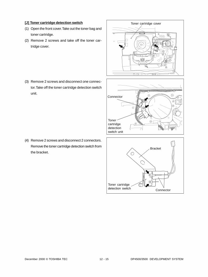
December 2000 © TOSHIBA TEC 12 - 15 DP4500/3500 DEVELOPMENT SYSTEM
[J] Toner car tridg e detection s witc h
(1) Open the front cover. Take out the toner bag and
toner cartridge.
(2) Remove 2 screws and take off the toner car-
tridge cover.
(3) Remove 2 screws and disconnect one connec-
tor. Take off the toner cartridge detection switch
unit.
(4) Remove 2 screws and disconnect 2 connectors.
Remove the toner cartridge detection switch from
the bracket.
Toner cartridge cover
Connector
Tonercartridgedetectionswitch unit
Bracket
Connector
Toner cartridgedetection switch

DP4500/3500 DEVELOPMENT SYSTEM 12 - 16 December 2000 © TOSHIBA TEC
[K] Humidity sensor
(1) Open the front cover and take out the paper re-
ceiving tray.
(2) Remove 4 screws and take off the metal cover
of the system unit.
(3) Disconnect one connector of the humidity sen-
sor.
(4) Remove the humidity sensor in the direction of
the arrow while the part of the holder indicated
as A in the right figure is slightly lifted up.
Metal cover
Connector
Humidity sensor window
Humidity sensor
A
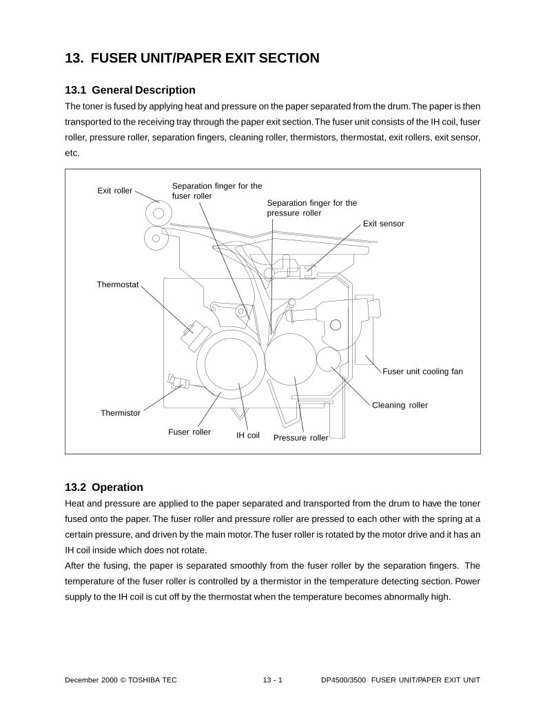
December 2000 © TOSHIBA TEC 13 - 1 DP4500/3500 FUSER UNIT/PAPER EXIT UNIT
Exit roller Separation finger for thefuser roller
Separation finger for thepressure roller
Exit sensor
Fuser unit cooling fan
Cleaning roller
Pressure rollerIH coilFuser roller
Thermistor
Thermostat
13. FUSER UNIT/PAPER EXIT SECTION
13.1 General DescriptionThe toner is fused by applying heat and pressure on the paper separated from the drum. The paper is then
transported to the receiving tray through the paper exit section. The fuser unit consists of the IH coil, fuser
roller, pressure roller, separation fingers, cleaning roller, thermistors, thermostat, exit rollers, exit sensor,
etc.
13.2 OperationHeat and pressure are applied to the paper separated and transported from the drum to have the toner
fused onto the paper. The fuser roller and pressure roller are pressed to each other with the spring at a
certain pressure, and driven by the main motor. The fuser roller is rotated by the motor drive and it has an
IH coil inside which does not rotate.
After the fusing, the paper is separated smoothly from the fuser roller by the separation fingers. The
temperature of the fuser roller is controlled by a thermistor in the temperature detecting section. Power
supply to the IH coil is cut off by the thermostat when the temperature becomes abnormally high.

DP4500/3500 FUSER UNIT/PAPER EXIT UNIT 13 - 2 December 2000 © TOSHIBA TEC
13.3 Functions(1) IH coil (IH: Induction Heating)
The IH coil is in the fuser roller and applies the induction heating to the fuser roller. The coil is fixed at
a position and does not move when the fuser roller is rotating.
(2) Fuser roller
The fuser roller is made of the iron and induction-heated by the IH coil. The fuser roller is in contact with
the below-mentioned pressure roller, and fusing is performed by passing the sheet of paper between
these two rollers. At this time, the toner image on the paper faces the fuser roller. Toner is melted by the
heat of fuser roller while the heat conductivity is improved by the pressure from the pressure roller, and
the toner soaks into the fibers of the paper.
The surface of the fuser roller is coated with the fluoroplastic to prevent the toner from adhering onto
the roller ( the phonomenon called “offset”) and to help the separation of the toner from the fuser roller.
(3) Pressure roller
The pressure roller is made of the silicon sponge which is highly cohesive and always pressed against
the fuser roller by springs.
(4) Separation finger
The separation fingers for the fuser and pressure rollers separate paper adhering to the fuser roller and
pressure roller.
(5) Cleaning roller
A metal cleaning roller is attached in contact with the pressure roller to remove the toner and paper
scraps sticking to the pressure roller.
(6) Exit sensor
This sensor detects the arrival of the leading edge or trailing edge of paper at the exit roller of the fuser
unit. It is also used to detect paper jams in the fuser unit paper discharge area and of the trailing edge
of the paper turned over for duplex copying.
(7) Fuser roller center thermistor
The thermistor detects the temperature of the fuser roller to maintain it within a certain temperature
range (the actual temperature is around 180°C) which is higher than the lower limit (the temperature
which causes the poor fusing) and lower than the upper limit (the temperature which causes the toner
offset). Thus, the thermistor controls the temperature of the fuser roller to turn on the IH coil when it is
lower than the set temperature and turn it off when it is higher than that.

December 2000 © TOSHIBA TEC 13 - 3 DP4500/3500 FUSER UNIT/PAPER EXIT UNIT
(8) Fuser roller side thermistor
The temperature distribution of the fuser roller may differ significantly at the center area and end area
in the lengthwise direction depending on the printing conditions. The side thermistor detects the tem-
perature of the end area. This center and side thermistors control the temperature to cut off the power
supply to the IH coil when either values detected by them exceeds the set temperature.
(9) Thermostat
The thermostat cuts off the power supply to the IH coil if the fuser roller becomes abnormally hot as a
result of any problems such as thermistor malfunction. The thermostat for this copier is used to prevent
abnormal operation. When the thermostat detects any abnormality, the thermostat must be replaced
together with the other damaged parts in the fuser unit.

DP4500/3500 FUSER UNIT/PAPER EXIT UNIT 13 - 4 December 2000 © TOSHIBA TEC
13.4 Heater Control Circuit13.4.1 Configuraton
[Blo
ck d
iagr
am o
f fus
er u
nit a
nd IH
con
trol
circ
uit]
NL
CP
U
LGC
IH
5V S
W
5V S
W
Sid
eth
erm
isto
r
Cen
ter
ther
mis
tor
Fus
er r
olle
r
The
rmos
tat
Co
il
Pow
er c
ode
Bre
aker
No
ise
filte
r
Fus
e
AC
inpu
tC
oil
outp
ut IH p
ower
sou
rce/
driv
e ci
rcui
t
Con
trol
circ
uit
incl
udin
g C
PU
Pho
toco
uple
r
AC
lin
e
DC
lin
e
Pow
er s
uppl
y fo
rph
otoc
oupl
er
Ele
ctric
pow
er s
ettin
g
Err
or s
igna
l
IH O
N/O
FF s
igna
l (L:
ON
)
Dru
mth
erm
isto
r
Tem
pera
ture
cont
rol
circ
uit
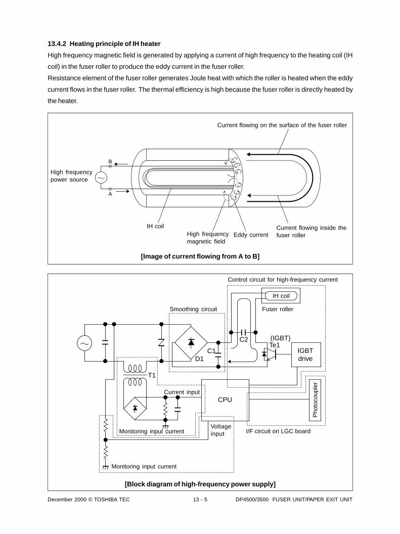
December 2000 © TOSHIBA TEC 13 - 5 DP4500/3500 FUSER UNIT/PAPER EXIT UNIT
13.4.2 Heating principle of IH heater
High frequency magnetic field is generated by applying a current of high frequency to the heating coil (IH
coil) in the fuser roller to produce the eddy current in the fuser roller.
Resistance element of the fuser roller generates Joule heat with which the roller is heated when the eddy
current flows in the fuser roller. The thermal efficiency is high because the fuser roller is directly heated by
the heater.
[Image of current flowing from A to B]
B
A
Current flowing on the surface of the fuser roller
High frequencypower source
IH coilHigh frequencymagnetic field
Eddy currentCurrent flowing inside thefuser roller
[Block diagram of high-frequency power supply]
D1
T1
C1
C2
CPU
Te1(IGBT)
IGBTdrive
IH coil
Fuser roller
Monitoring input current
Monitoring input current
Current input
Voltageinput I/F circuit on LGC board
Pho
toco
uple
rSmoothing circuit
Control circuit for high-frequency current

DP4500/3500 FUSER UNIT/PAPER EXIT UNIT 13 - 6 December 2000 © TOSHIBA TEC
13.4.3 IH control circuit interface
The IH control circuit uses a photocoupler as insulation against the secondary circuit.
The interface signals are as follows.
(*Note) IH status signal
• When the temperature (due to insufficient cooling) of the switching element (IGBT) is abnor-
mal:
“10: Abnormal temperature, IH-FAN stopped” n After a certain period of time n Error[C48]
• When the upper limit of the power voltage is abnormal: “00: Initializing” n After a certain
period of time n Error[C47]
• When the lower limit of the power voltage is abnormal: “00: Initializing” n After a certain
period of time n Error[C47]
• Defective circuits n: “11” Abnormal circuit, defective coil n Error[C49]
• Standby state after initialization: “01: Ready”
No. Name of signal Direction Definition
J522-1 5V
J522-2 PWR3 Host to IH
J522-3 PWR2
J522-4 PWR1
J522-5 IH ON/OFF Host to IH Thermistor monitoring feedback signal from host
J522-6 ERROR2 IH to Host IH status signal (*Note)
J522-7 ERROR1 (ERROR2 ERROR1)
J522-8 GND

December 2000 © TOSHIBA TEC 13 - 7 DP4500/3500 FUSER UNIT/PAPER EXIT UNIT
13.4.4 Relation between system configuration and IH output
* FIN: Finisher, FAX: Fax unit, PRT: Printer unit, SC: System controller
(*1) The electric power is lowered when a document fed from the ADF is scanned while the copier is
warming up.
(*2) AC power should be 100V when the copier is warming up (the lower the voltage, the longer the
warming up time becomes).
13.4.5 Abnormality of IH control circuit
IH output is stopped when the IH control circuit does not work properly.
(1) When the power voltage of the copier is too high or too low
IH output is stopped to protect the IGBT when the input voltage which is higher or lower than specified
range is applied to the copier. This is an error [C47].
(2) When the AC is not applied to the IH control circuit
The AC is not applied to the IH control circuit properly. This is an error [C47]. The same error occurs
when the thermostat is activated (blown).
(3) When the temperature of the IGBT is too high
IGBT is forcibly cooled down by the fan as it becomes hot when the power is supplied to the IH control
circuit. The error [C48] is occurs when the cooling operation is not sufficient and the IGBT gets too hot.
System configuration Warming up Ready CopyingEnergy Automatically Warming
saver mode OFF up time
Copier only 1300/1250W 700W 900W 700W OFF Approx.
Copier and ADF(*1) 1250/1200W(*2) 30 sec.
Copier, ADF(*1) and FIN 1250/1200W Approx.
Copier, ADF(*1) and FAX 1200/1100W(*2) 40 sec.
or
Copier, ADF(*1), FAX
and PRT
Copier, ADF(*1), FIN, 1200/1100W Approx.
FAX and PRT 45 sec.
Copier, ADF(*1) and SC
Copier, ADF(*1), FIN, 1100/1100W Approx.
FAX and SC 50 sec.

DP4500/3500 FUSER UNIT/PAPER EXIT UNIT 13 - 8 December 2000 © TOSHIBA TEC
(4) The temperature detection sensor of the IH control circuit is malfunctioning
The error [C49] occurs when the temperature detection sensor of the IH control circuit does not work
properly.
The same error code is displayed in case the IH coil is not connected properly.
13.4.6 Temperature detection section
To keep the fuser roller temperature constant, the thermistors detect the temperature and control ON/OFF
of the heater. Output from the thermistors is used to detect abnormality.
(1) Relation between the thermistor output voltage and surface temperature of the fuser roller:
Approx. 4.0V when the temperature is 200°C, and approx. 0.5V when the temperature is 40°C.
Approx. 3.7V when the temperature is 180°C, and approx. 3.9V when the temperature is 190°C.
(2) Control of the surface temperature of the fuser roller:
C
190180
OFF ON OFF ON OFF ON OFF ON OFF OFFON
(3) Temperature control for both ends of the fuser roller
During the multiple copying, the temperature of both ends of the fuser roller (areas where the paper
does not pass) generally tends to become higher than that of the other areas (areas where the paper
passes). The temperature of the ends is detected by the side thermistor, and when it reaches 250°C,
the heater is automatically turned OFF regardless of the temperature of the area where the paper
passes.
(4) Error detection during warming up (1)
If the output voltage of the thermistor does not go over approx. 0.5V(40°C) even a certain period of time
has passed after the heater was turned ON, service call [C41] is displayed.
(5) Error detection during warming up (2)
If the output voltage of the thermistor does not go over approx. 3.2V(150°C) after it exceeded 40°C and
a certain period of time has passed, service call [C44] is displayed.
Warming-up Ready (190°C) During copying (180°C)
Temperatureof fuser roller
Heater ON

December 2000 © TOSHIBA TEC 13 - 9 DP4500/3500 FUSER UNIT/PAPER EXIT UNIT
(6) Error detecion during standby and copying
Service call [C43] is displayed if the output voltage of the center thermistor becomes approx. 0.5V or
lower for 0.5 sec. or longer. If the side thermistor is in this condition, service call [C45] is displayed.
(7) Error detection during warming up (3)
If the output voltage of the thermistor does not go over approx. 3.9V(190°C) after it exceeded 150°C
and a certain period of time has passed, service call [C44] is displayed.
(8) Thermistor/heater status counter control
• To enhance the safety of the fuser unit, the CPU provides the following protection: When the third
[C41] error has occurred after two consecutive [C41] errors, even if the operator turns the power OFF
and then back ON, the heater is not turned ON and error [C41] is displayed immediately.
However, if the copier becomes ready normally with the thermistor/heater status counter “1” or below,
the counter is cleared to “0”.
• If the heater is not turned ON and any of the error codes [C41] to [C45] is still displayed even though
the thermistor, thermostat and IH coil have been repaired and the power is turned ON, check the
code “400” in the mode (08) to set the thermistor/heater status counter to “0”.
Reference
* The thermistor/heater status counter never has values other than 0 ~ 19 entered.
• If the heater does not come ON and service call [C41] is displayed immediately after the power
is turned ON, check the thermistor/heater status counter. If it is “2” or over, be sure to check the
thermistor, thermostat and IH coil. Reset the counter to “0” (code “400” in the (08) mode) after
repairing them, then turn ON the power.
• If the thermistor/heater status counter is “20” or over (e.g., 21), there is a possibility that data in
BCRAM or BCRAM itself may have been ruined due to causes such as leakage from the charg-
ers. Check the bias, high-voltage transformers and charge wires to see if any of them is defec-
tive, and also look through all the data in the BCRAM.

DP4500/3500 FUSER UNIT/PAPER EXIT UNIT 13 - 10 December 2000 © TOSHIBA TEC
13.4.7 Detection of open-circuited thermistors
A thermistor is a device whose resistance decreases when it detects high temperature. If the fuser roller
thermistor is open-circuited, the control circuit determines that the fuser roller temperature is extremely
low, and keep turning ON the IH coil. As the result, the fuser roller temperature rises, possibly activating
the thermostat which is a safety protection device. To prevent this, CPU works to detect if the thermistor is
open-circuited or not.
* The following is a circuit diagram of the thermistor open-circuit detection circuit for the center thermistor.
The same circuit is used for the side thermistor.
· The input voltage is obtained by dividing the resistor-1, thermistor, resistor-2 and resistor-3.
· The surface temperature of the fuser roller changes.
x
The resistance of the thermistor changes.
x
The input voltage changes.
· The main CPU detects this change of the input voltage to determine if the thermistor is abnormal or not.
Center thermistor
Main CPUR165
+5
R170
R174
C125
HTRTH-
Resistor-1
Resistor-2
Resistor-3

December 2000 © TOSHIBA TEC 13 - 11 DP4500/3500 FUSER UNIT/PAPER EXIT UNIT
13.4.8 Control for abnormal heater conditions
The heater cannot be turned ON/OFF when trouble occured to the IH control circuit. In this case, the
microcomputer detects abnormal temperature using the center and side thermistors, determines the corre-
sponding error codes and counter values. The power is then turned OFF to protect the fuser unit in case the
machine is 200V-series.
(1) Temperature to be detected
Abnormal temperature detected by the thermistors:
Center thermistor: 230°C
Side thermistor: 270°C
(2) Error code
[C44] “Call for service” : Displayed when the keys [C/S] and [8] are pressed simultaneously.
Counter value “9” : Displayed by entering the code number “400” in the setting mode (08).
(3) Operation of the machine
The microcomputer stops the output of the heater, exposure lamp, control panel display and motor,
then turns OFF the power in case the machine is 200V-series.
(4) Corrective action
[For 200V-series]
Thermistors continue detecting the abnormal temperature even after the error codes and counter val-
ues are determined. Even if the power is turned ON by the operator, it is automatically turned OFF
when the surface temperature of the fuser roller is still abnormal or higher than the temperature in (1).
This behavior is repeated until the temperature becomes normal.
Wait until the surface temperature of the fuser roller is lowered enough, and turn ON the power to check
the counter value.
[For 200V-series and other models]
The copier is returned to the normal conditions by fixing the heater and setting the counter value of the
setting code from “400” to “0”.

DP4500/3500 FUSER UNIT/PAPER EXIT UNIT 13 - 12 December 2000 © TOSHIBA TEC
13.5 Exit Motor DriveThe control circuit of the exit motor which works to drive the exit roller is shown below.
The exit motor is a 4-phase control PM stepping motor. The motor is turned ON/OFF and the direction of its
rotation is changed by controlling the timing of the pulse signal output (A·A·B·B).
+24A
PWA-F-LGC-320
CPUIC13
Exitmotor
MotordriverIC35
EXTMA-0
EXTMB-0
EXTMC-0
EXTMD-0
A
B
A
B

December 2000 © TOSHIBA TEC 13 - 13 DP4500/3500 FUSER UNIT/PAPER EXIT UNIT
13.6 Disassembly and Replacement[A] Fuser unit
(1) Remove 2 screws and take off the feed side
upper cover.
(2) Disconnect 2 connectors and 2 faston terminals.
(3) Open the jam access cover.
(4) Remove 2 blue screws and take out the fuser
unit.
[B] Fuser unit cooling fan
(1) Release the hooks near the hinges and take off
the fuser unit cover.
Connector and faston terminal (2 each)
Jam access cover
(2) Disconnect one connector, remove 2 screws and
release 2 latches. Take off the fuser unit cooling
fan.
(3) Release 2 latches and remove the fan cover.
(4) Release the harness from the holder.
Remove 4 screws and take off the fuser unit
cooling fan.
Connector
Latch
Latch
Fan cover
Fuser unit cover Hook
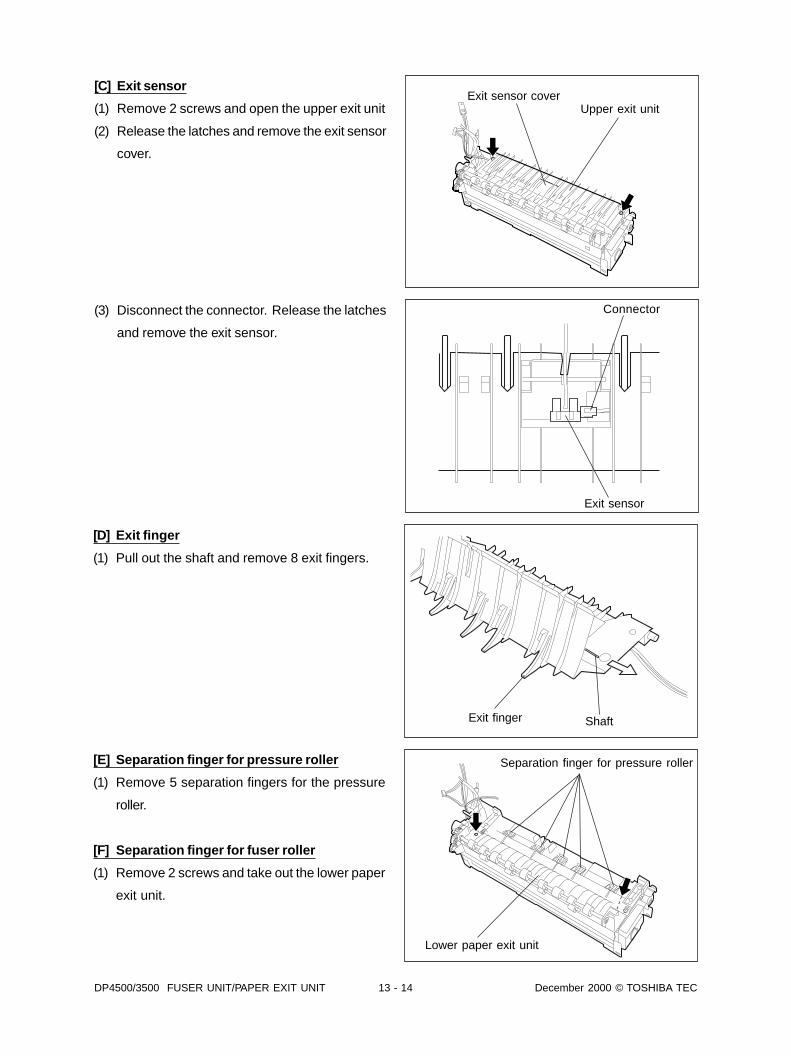
DP4500/3500 FUSER UNIT/PAPER EXIT UNIT 13 - 14 December 2000 © TOSHIBA TEC
[C] Exit sensor
(1) Remove 2 screws and open the upper exit unit
(2) Release the latches and remove the exit sensor
cover.
(3) Disconnect the connector. Release the latches
and remove the exit sensor.
Exit sensor coverUpper exit unit
Connector
Exit sensor
[D] Exit finger
(1) Pull out the shaft and remove 8 exit fingers.
[E] Separation finger for pressure roller
(1) Remove 5 separation fingers for the pressure
roller.
[F] Separation finger for fuser roller
(1) Remove 2 screws and take out the lower paper
exit unit.
Exit finger Shaft
Separation finger for pressure roller
Lower paper exit unit

December 2000 © TOSHIBA TEC 13 - 15 DP4500/3500 FUSER UNIT/PAPER EXIT UNIT
(2) Remove 6 separation fingers for the fuser roller.
[G] Cleaning roller
(1) Remove one screw and take off the rear side
cover.
Separation fingerfor fuser roller

DP4500/3500 FUSER UNIT/PAPER EXIT UNIT 13 - 16 December 2000 © TOSHIBA TEC
(2) Remove the screws from the front and rear sides
(2 each). Take off the stay of the pressure roller
side.
(3) Remove the E-ring. Take off the cleaning roller
together with the bushings at the both sides.
Stay
Cleaning rollerBushing
E-ring
[Rear side]
[Front side]

December 2000 © TOSHIBA TEC 13 - 17 DP4500/3500 FUSER UNIT/PAPER EXIT UNIT
[H] Pressure roller
(1) Take off the pressure springs of the front and
rear sides from the hooks.
(2) Take off the pressure roller.
[I] IH coil
(1) Remove 2 screws and take off the front coil
holder.
(2) Remove one screw and take off the rear coil
holder.
Pressure spring
Pressure roller
Front coil holder
Rear coil holder

DP4500/3500 FUSER UNIT/PAPER EXIT UNIT 13 - 18 December 2000 © TOSHIBA TEC
(3) Pull out the IH coil from the rear side.
[J] Fuser roller
(1) Remove the grip ring of the front side.
(2) Remove the E-ring of the rear side and take off
the gear A.
(3) Remove the grip ring and gear of the rear side.
(4) Take off the fuser roller.
Notes: 1. Do not deform the thermistor when
installing the fuser roller.
2. Pay attention to the direction of the gear
(the position of a square protrusion on the
inner face of the gear) when attaching it.
IH coil
Fuser rollerGrip ring
[Front side]
[Rear side]
Grip ringGearFuser roller
Gear A
Outer edge(Grip ring side)
Protrusion
Inner edge(Bearing side)

December 2000 © TOSHIBA TEC 13 - 19 DP4500/3500 FUSER UNIT/PAPER EXIT UNIT
[K] Thermistor
(1) Remove one screw and take off the center ther-
mistor.
(2) Remove one screw and take off the side ther-
mistor.
Note: Do not deform or damage the thermistors
and frame (metal sheet) when fixing the
thermistors.
[L] Thermostat
(1) Remove 2 screws and take off the thermostat.
Sidethermistor
Center thermistor Thermostat
Notes: 1. Give attention to the order to fix the ther-
mostat terminal and harness terminal
when fixing the thermostat with a screw.
2. Adjust space between the fuser roller and
thermostat by tightening/loosening the
screw A while the pressure roller is
pressed against the fuser roller to make
the space fall within 1.5 to 1.9mm.
[M] IH control board cooling fan
(1) Take off the rear side upper and lower covers.
(2) Disconnect one connector and remove 2 screws.
Take off the IH control board cooling fan together
with the sheet metal.
(3) Remove 2 screws and take the IH control board
cooling fan apart from the sheet metal.
Note: Pay attention to the direction of the air flow
from the fan when installing it.
IH control board cooling fan
Connector
Screw A
Harness terminalScrew Thermostat

DP4500/3500 FUSER UNIT/PAPER EXIT UNIT 13 - 20 December 2000 © TOSHIBA TEC
[N] IH control board
(1) Disconnect 4 connectors and remove 9 screws.
Take off the IH control board.
[O] Exit motor
(1) Remove 2 screws and take off the case of the
IH control board (Slide the case to the right to
detach the hooks, then take off the case).
Note: If the IH control board is not replaced with
new one, the board does not have to be sepa-
rated from the case.
(2) Disconnect one connector and remove 2 screws.
Take off the exit motor behind the sheet metal
with the bracket attached.
(3) Remove 2 screws and take off the exit motor.
ConnectorIH controlboard
Connector
Exit motor
[O]
[O]

December 2000 © TOSHIBA TEC 14 - 1 DP4500/3500 AUTOMATIC DUPLEXING UNIT
14. AUTOMATIC DUPLEXING UNIT (ADU)
14.1 General DescriptionThe Automatic Duplexing Unit (ADU) is a unit which automatically makes a copy on both sides of a sheet
of paper.
The switchback method is adopted for the ADU of this model.
The sheet of paper is switchbacked right after the copying operation (fusing process) on one side is
completed, and the reversed paper is transported to the registration section to be copied on another side.
The ADU mainly consists of the transport rollers and their drive system, paper transport guide and the
ADU entrance/exit sensors.
Lower transport roller
Exit guide
ADU exit sensor
ADU motor
Middle transport roller
ADU entrance sensor
Entrance guide
Upper transport roller
Paper guideExit gate

DP4500/3500 AUTOMATIC DUPLEXING UNIT 14 - 2 December 2000 © TOSHIBA TEC
14.2 Description of OperationsThe back side copying (data for the back side of a paper is recorded) is performed by first selecting the
duplex copying mode and pressing the START key. When the trailing edge of the paper passes the exit
gate, the paper is switchbacked and transported to the ADU (the exit gate is closed by its own weight) then
to the registration section, and the front side copying (data for the front side of the paper is recorded) is
performed. The paper passes through the exit gate again and is transported to the paper receiving tray to
complete duplex copying.
There are three kinds of jams which are related to the ADU.
E51: The ADU entrance sensor does not come ON within a fixed time after the switchback operation has
been started in the ADU.
E52: The ADU exit sensor does not come ON within a fixed time after the ADU entrance sensor has
become ON.
E11: The registration sensor does not come ON within a fixed time after the ADU has started feeding paper
into the main unit.
The error [E43] occurs if the ADU is opened during duplex copying. The ADU motor and ADU clutch are
stopped at this time.
If the copying operation is interrupted or stopped for some reason other than jam or service call, the
process in progress on a sheet of paper is completed and the sheet is discharged into the paper receiving
tray.
The operation of the duplex copying varies depending on the size of the paper: Single-sheet circulation and
Double-sheet circulation.
The figure on the following pages show the duplex copying operation when documents from page one to
four are copied. The numbers in the figure indicate the page numbers.

December 2000 © TOSHIBA TEC 14 - 3 DP4500/3500 AUTOMATIC DUPLEXING UNIT
(a) Single-paper circulation
With sheets of paper other than A4/LT size, duplex copying (back-side copying n front-side copying) is
performed for a single sheet of paper as shown below.

DP4500/3500 AUTOMATIC DUPLEXING UNIT 14 - 4 December 2000 © TOSHIBA TEC
(b) Double-sheet circulation
With A4/LT sized paper, duplex copying is performed for two sheets of paper at a time as shown below. The
sheets are processed in the following order.
Back side of the 1st sheet n back side of the 2nd sheet n front side of the 1st sheet n front side of
the 2nd sheet

December 2000 © TOSHIBA TEC 14 - 5 DP4500/3500 AUTOMATIC DUPLEXING UNIT
2236
326
204
1262
036
220
3222
6823
0024
30
4382
4560
3826
6640
7036
8060
9010
9354
1055
812
432
5708
7096
8060
9010
9354
1128
212
432
4970
6916
7580
1053
411
696
1274
0
5304
6602
7910
1112
212
030
5718
5942
7642
7762
2272
3480
4490
6670
7680
7982
8992
1028
811
298
1249
413
504
2018
2226
4236
5900
8738
2204
2394
4420
5632
7606
7726
8926
9278
1122
412
356
1343
0
3320
4460
5532
7650
8716
8962
1004
011
264
1234
413
470
1453
8
Timing chart for duplex copying on 3 A4 sized sheets fed from the upper cassette
In t
he m
ain
unit
Exi
t se
nsor
Reg
istr
atio
nse
nsor
Upp
er c
asse
ttefe
ed s
enso
r
Reg
istr
atio
ncl
utch
Tran
spor
t cl
utch
(low
spe
ed)
In th
e A
DU
AD
U e
ntra
nce
sens
or
AD
U e
xit
sens
or
AD
U c
lutc
h
AD
U m
otor

DP4500/3500 AUTOMATIC DUPLEXING UNIT 14 - 6 December 2000 © TOSHIBA TEC
Timing chart for duplex copying on one A3 sized sheet fed from the upper cassette
In t
he m
ain
unit
Exi
t se
nsor
Reg
istr
atio
n se
nsor
Reg
istr
atio
n cl
utch
In th
e A
DU
AD
U e
ntra
nce
sens
or
AD
U e
xit
sens
or
AD
U c
lutc
h
AD
U m
otor
975
1920
019
80
4110 42
70
3550
5425
5485
6860
5425
5485
6860
4690
6680
6000
5485
7465
5345
7380
3035
6445
8500

December 2000 © TOSHIBA TEC 14 - 7 DP4500/3500 AUTOMATIC DUPLEXING UNIT
14.3 Drive of ADUWhen the ADU motor rotates in the direction A, the upper transport roller is rotated driven by the gears and
belt. The ADU clutch is then turned ON, allowing the middle transport roller and lower transport roller to
rotate.
Upper transport roller
Middle transport roller
ADU motor
ADU clutch
Lower transport roller
A

DP4500/3500 AUTOMATIC DUPLEXING UNIT 14 - 8 December 2000 © TOSHIBA TEC
14.4 Flow Chart
Yes
No
Yes
No
Yes
A
No
Exit motor reverserotation ON
400msec. elapses
ADU motor ON
ADU entrancesensor ON?
ADU transport jam(E51)
32msec. elapses(A sheet is transported to the positionwhere the sheets are stopped first.)
The trailing edgeof the first sheet turned
ON the ADU exitsensor?
ADU motor stopped
ADU motor ON
ADU clutch ON
ADU exit sensor ON?
400msec. elapses
ADU transport jam(E52)

December 2000 © TOSHIBA TEC 14 - 9 DP4500/3500 AUTOMATIC DUPLEXING UNIT
Yes
No
Yes
No
A
ADU paper feedingcommand signal
received
ADU motor stoppedADU clutch OFF
ADU motor/clutch ON
ADU feedingoperation started
Registrationsensor ON?
ADU misfeeding(E11)
Registrationproceeded
Registration operationcompleted
ADU motor stoppedADU clutch OFF
Next paper is readyfor the registration

DP4500/3500 AUTOMATIC DUPLEXING UNIT 14 - 10 December 2000 © TOSHIBA TEC
14.5 Disassembly and Replacement[A] ADU
(1) Remove the feed side rear hinge cover and feed
side front hinge cover.
(2) Open the ADU.
(3) Disconnect one connector and remove one screw
fixing the ground wire. Remove the pin.
(4) Slide the ADU to the rear side and take it off.
[B] ADU inside cover
(1) Remove 2 screws and take off the ADU inside
cover (front).
(2) Remove 2 screws and take off the ADU inside
cover (rear).
[C] ADU opening/closing switch
(1) Disconnect the connector. Release the latches
and take off the ADU opening/closing switch.
[D] ADU cover
(1) Remove 4 screws and take off the ADU cover.
Note: Make sure to attach the ADU opening/clos-
ing switch when attaching the ADU cover.
ADU inside cover (rear) ADU inside cover (front)
Connector
Pin
ADU opening/closing switch

December 2000 © TOSHIBA TEC 14 - 11 DP4500/3500 AUTOMATIC DUPLEXING UNIT
[E] Paper guide
(1) Detach the fulcrum at the rear side from the
frame.
Take off the paper guide.
(2) Release the hook springs and remove the pinch
rollers (6 each).
(3) Remove 2 screws and take off 2 pressure plate
springs.
[F] Latches
(1) Remove the spring.
(2) Remove one screw and take off the front latch.
(3) Remove the screw and take off the rear latch.
Front latch
Spring
Rear latch
Pressure plate spring Pinch rollerHook spring
Fulcrum

DP4500/3500 AUTOMATIC DUPLEXING UNIT 14 - 12 December 2000 © TOSHIBA TEC
[G] Opening/closing lever
(1) Remove 2 screws and take off the opening/clos-
ing lever.
[H] ADU entrance sensor and ADU exit sensor
(1) Disconnect the connector. Release the latches
and remove the ADU entrance sensor.
(2) Disconnect the connector. Release the latches
and remove the ADU exit sensor.
[I] ADU board
(1) Remove 4 screws and take off the bracket. Dis-
connect one connector of the harness connected
with the ADU board from the bracket.
Opening/closing lever
Lock supportADU board
ADU motor
(2) Disconnect 5 connectors. Release 4 lock sup-
ports and take off the ADU board.
[J] ADU motor
(1) Remove 2 screws and take off the ADU motor.
ADU entrance sensor
ADU exit sensor
Bracket

December 2000 © TOSHIBA TEC 14 - 13 DP4500/3500 AUTOMATIC DUPLEXING UNIT
[K] ADU drive unit
(1) Remove 3 screws and take off the gear unit.Gear unit
(2) Remove 2 E-rings and take off 3 gears.
(3) Disconnect one connector. Loosen one setscrew
and take off the ADU clutch.
[L] ADU transport rollers and entrance/exit guides
(L-1) Upper transport roller
(1) Remove 4 screws and take off the bracket.
E-ring
Connector
Setscrew

DP4500/3500 AUTOMATIC DUPLEXING UNIT 14 - 14 December 2000 © TOSHIBA TEC
(2) Remove the clip of the front side.
(3) Remove the clip, pulley, fixing pin and belt of
the rear side.
(4) Remove 2 bushings and take off the upper
transport roller.
(L-2) Middle transport roller
(1) Remove the clip, pulley, fixing pin and belt of
the front side.
(2) Remove the clip of the rear side.
(3) Remove 2 bushings and take off the middle
transport roller.
(L-3) Entrance guide
(1) Remove 4 screws (2 each for front and rear sides)
and take off the entrance guide.
(L-4) Lower transport roller
(1) Remove the clip, pulley, fixing pin and belt of
the front side.
(2) Remove the clip of the rear side.
(3) Remove 2 bushings and take off the lower
transport roller.
(L-5) Exit guide
(1) Remove 3 screws (2 for the front side and 1 for
the rear side) and take off the exit guide.
[Front side]
[Rear side]
[Front side]
[Rear side]
Bushing (L-4)
Clip (L-4)
(L-5)
Clip (L-1)
Bushing (L-1)
Clip (L-2)
Pulley (L-2)
Bushing (L-2)
(L-3)
(L-3)
Fixing pin(L-2)
Bushing(L-4)
Pulley (L-4)
Exit guide
Clip (L-4)
(L-5)
(L-5)Fixing pin(L-4)
Bushing(L-1)
Pulley (L-1)
Clip (L-1)
Entrance guide
(L-3)
(L-3)
Clip (L-2)
Bushing (L-2)
Fixing pin (L-1)

December 2000 © TOSHIBA TEC 15 - 1 DP4500/3500 POWER SUPPLY UNIT
15. POWER SUPPLY UNIT
15.1 ConfigurationThe power supply unit consists of an AC filter and insulation type DC output circuits.
(1) AC filter
Eliminates noise from the outside and prevents noise generated by the copier from leaking to the outside.
(2) DC output circuits
The DC outputs are roughly divided into three lines of outputs:
a. System line : Power supply used around-the-clock mainly for the SYS/FAX board. This line outputs
three voltage (+3.3V, +5.1V, +12V) which start up when the main switch is turned ON.
b. Main line : Power supply used in the entire machine during image forming process. This line
outputs four voltage (+3.3V, +5.1V, +12V and -12V) which are started up by the
signals from the SYS board.
c. Door switch line : Power supply used in the entire machine during image forming process, being sup-
plied via the door switch. This line outputs two voltage (+5V and +24V) which start up
when the door switch is turned ON and with the signals from the SYS board.

DP4500/3500 POWER SUPPLY UNIT 15 - 2 December 2000 © TOSHIBA TEC
15.2 Operation of DC Output Circuits(1) Start of operation
When the main switch of the copier is turned ON, AC power is supplied to the switching regulator-1 (REG
1) to start up three output voltage of the system line. System CPU is then activated to output the power
control signal (PWR-EN: “L” level), and four output voltage of the main line are started up. If the door switch
of the copier is ON (the door is closed) at this time, AC power is supplied to the switching regulator-2 (REG
2) to start up two output voltage of the door switch line.
(2) Stop of operation
When the main switch of the copier is turned OFF, the power-OFF signal (PWR-DN) is output (Hi-Z: High
impedance) after the instantaneous outage insurance time (20 msec. at least) has elapsed. After the
power-OFF signal has been output, the regulator-1 (system line and main line) retains the rated voltage for
the minimum retaining time (15 msec. at least, depending on the AC input and load capacity), then starts
to drop the voltage.
(3) Output protection
Each output system includes an over-current protection circuit (which has the fuse protecion and the series
regulator internal protection functions) and an over-voltage protection circuit (does not cover the voltage
±12V of the system/main lines). These circuits prevent the abnormal operation or damage to the secondary
circuit caused by over-current due to shorted load or over-voltage due to short-circuit between different
voltages.
When the protection circuit is activated, remove the causes such as short-circuits (replace the fuse if it is
blown), and turn ON the power again to clear the circuit. Occasionally it may not cleared when the power is
turned back ON too soon (within 30 seconds).

December 2000 © TOSHIBA TEC 15 - 3 DP4500/3500 POWER SUPPLY UNIT
15.3 Output ChannelThe following are 3 output channels which are not linked with the door switches.
(1) 3.3V
3.3VA : Pin 1, J412
Output to the LGC board
3.3VB : Pins 1, 2 and 3, J413
Output to the SYS board
3.3VC : Pin 1, J414
Output to the SLG board and CCD board via SLG board
3.3VD : Pin 4, J413
Output to the SYS board
(2) 5.1V
5.1VA : Pins 3 and 4, J412
Output to the LGC board
5.1VB : Pins 17, 18, 19 and 20, J413
Output to the SYS board
5.1VC : Pin 21, J413
Output to the SYS board
5.1VD : Pins 3 and 4, J414
Output to the SLG board, SDV/CCD board (via SLG board) and FUS board
5.1VE : Pin 5, J414
Output to the RADF and finisher
5.1VF : Pin 6, J414
Output to the RADF and finisher
(3) 12V
12VA : Pin 24, J413
Output to the SYS board
-12VA : Pin 26, J413
Output to the SYS board
12VB : Pin 25, J413
Output to the SYS board
12VC : Pin 11, J414
Output to the SLG board and CCD board via SLG board

DP4500/3500 POWER SUPPLY UNIT 15 - 4 December 2000 © TOSHIBA TEC
The following are 2 output channels which are linked with the door switches.
(1) 5.1V
5.1VG : Pin 5, J416
Output to the LGC board
(2) 24V
24VC : Pin 1, J415
Output to the SLG board and SDV board via SLG board
24VD : Pin 2, J415
Output to the RADF and finisher
24VE : Pin 3, J415
Output to the RADF and finisher
24VF : Pin 1, J416
Output to LGC board (MOT, FAN, ADU and CLT)
24VG : Pin 2, J416
Output to LGC board (MOT, FAN, relay unit and high-voltage transformer)
<<Output connector>>
Not linked with the door switches
J412 for the LGC board
J413 for the SYS board
J414 for the SLG board, SDV board, RADF and finisher
Linked with the door switches
J415 for the SLG board, SDV board, RADF and finisher
J416 for the LGC board, MOT, FAN, ADU, CLT, relay unit and high-voltage transformer

December 2000 © TOSHIBA TEC 15 - 5 DP4500/3500 POWER SUPPLY UNIT
[Configuration of power supply unit]
Noisefilter
Noisefilter
Noisefilter
IH
REG2
F1
F2
F3
F4
F5
F6
F7
24VC (SCN)
5.1VGPWR-EN
24VD (RADF/FIN)
24VE (RADF/FIN)
24VF
24VG
REG1
3.3VA/5.1VA (M)
3.3VB.D/5.1VB, C (SYS)
3.3VC/5.1VD (SCN)
5.1VE, F (RADF/FIN)
12VA, B (SYS)
–12VA (SYS)
12VC (SCN)
PWR-DN
Breaker Main switch
Door switch
Switchingpower supply

DP4500/3500 POWER SUPPLY UNIT 15 - 6 December 2000 © TOSHIBA TEC
AC input
ON (Instantaneous outage)
[Sequence of power supply]
Max. 20ms
OFF
120ms or lower
PWR-DNsignal
20ms or higher
50ms or higher500ms or lower
System lineoutput (withrated load)
200ms or lower
Lower limit of eachrated voltage or higher
Hi-Z(Highimpedance)
200ms or lower
PWR-EN signal
Main line outputDoor switch line output(with rated load)
(L)
Lower limit of eachrated voltage or higher
(L)
Hi-Z (High impedance)

December 2000 © TOSHIBA TEC 16 - 1 DP4500/3500 PC BOARDS
16. PC BOARDS
(1) PWA-F-SYS-320

DP4500/3500 PC BOARDS 16 - 2 December 2000 © TOSHIBA TEC
(2) PWA-F-LGC-320
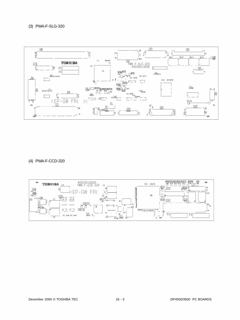
December 2000 © TOSHIBA TEC 16 - 3 DP4500/3500 PC BOARDS
(3) PWA-F-SLG-320
(4) PWA-F-CCD-320

DP4500/3500 PC BOARDS 16 - 4 December 2000 © TOSHIBA TEC
(5) PWA-F-SDV-320
(6) PWA-F-LDR-320
(7) PWA-F-SNS-320

December 2000 © TOSHIBA TEC 16 - 5 DP4500/3500 PC BOARDS
(8) PWA-F-ADU-520-3
(9) PWA-F-FUS-320

DP4500/3500 PC BOARDS 16 - 6 December 2000 © TOSHIBA TEC