dr. louise senguptamy.ece.ucsb.edu/york/yorklab/projects/ferroelectrics/ims2000... · dr. louise...
TRANSCRIPT

Dr. Louise SenguptaDr. Louise SenguptaDr. Louise SenguptaDr. Louise SenguptaPresident & CEO
Paratek Microwave, Inc.6935N Oakland Mills RoadColumbia, MD 21045www.paratek.com

The Tunable Wireless Company
• We build tunable filters and electronically scanning antennas for wireless networks.
• Our electronically tunable RF (ETRF TM ) products increase capacity and data rates, while reducing system deployment costs.

Parascan™ Technology
Patented tunable dielectric materials are thecornerstone of our technology.
Materials can be fabricated for bulk, thick film andthin film components.
Continual pursuit of new compositions for component development.

Tunable FiltersElectronically Steerable
Tracking Antennas
•Beam Tilt (PCS) Antennas•Tunable Delay Lines for Power Amplifiers•Advanced Military Radar
•Multifrequency Radios(33 MHz-40 GHz)
•Steerable LMDS Hub Antennas•Satellite Tracking Antennas
•Mobile Satellite•Mobile Subscriber
Phase Shifters
Product Family and Applications

Measured Loss Tangent of a PARASCANTM Composite
Freq (MHz) Loss Tangent1 0.00024
542 0.00096700.7 0.0014843.4 0.00143925 0.001345
1001 0.00149
0
0.0002
0.0004
0.0006
0.0008
0.001
0.0012
0.0014
0.0016
0 100 200 300 400 500 600 700 800 900 1000 1100
Frequency (MHz)
Loss
Tan
gent
of A
E-9
Courtney Resonator, NIST
Open Resonator, Rome Labs
Dielectric Sleeve Resonator, NIST
LCR Meter, Paratek
A linear relationshipis implied between
loss tangent andfrequency.

Tunability of a PARASCANTM CompositeDoubly-Reentrant Biased VHF/UHF Cavity
%100x:,
/2,,
unbiasedr
mVatbiasedrunbiasedrTTunabilityε
εε µ−=
Bias Field Tunability (%)(V/um) 10 KHz Tunability VHF Tunability
0 0 00.4 1.340.8 3.59 6.851.2 7.171.6 11.21 8.572 14.35
2.4 17.93 14.662.8 19.733.2 21.97 20.3853.6 23.774 27.53 25.764
0
5
10
15
20
25
30
0 1 2 3 4 5Electric Field (V/mm)
AE
-9 T
unab
ility
(%)
10 KHz TunabilityVHF Tunability
(40 MHz)(10 KHz)
TUNABILITY DOES NOT VARY WITH FREQUENCY

Tunability of a PARASCANTM Composite at High Field Strengths
0.40
0.45
0.50
0.55
0.60
0.65
0.70
0.75
0.80
0.85
0.90
0.95
1.00
0 1 2 3 4 5 6 7 8 9 10 11 12
Bias E Field (V/um)
Nor
mal
ized
Perm
ittiv
ity(εε εε
r/εε εεro
)
AE-9
Linear Approx. er/ero=-.0474E+1.0266
Note 1: Unbiased relative permittivity, εro, is 291.
Bias Field εr/εro0 1.00000.5 0.99841 0.98731.5 0.96672 0.93972.5 0.91273 0.88573.5 0.86034 0.83494.5 0.81435 0.79055.5 0.76836 0.74606.5 0.72067 0.70167.5 0.67308 0.64298.5 0.6063
TUNABILITYIS LINEAR

Material FOM FOMCode (10GHz) (24GHz)
Y0 1.822 4.229X30 1.501 3.622Y111 3.47Y115 4.034Y122 3.126Y121 3.543Y120 1.549 3.407Y53 2.53 3.45Y126 3.573Y130 3.3Y131 3.472Y132 2.825Y129 3.43Y108 2.549 3.34Y85 2.95
W106 2.686
Figure of Merit (FOM) for ParascanTM Compositesat 10 GHz and 24 GHz

PARASCANTM Varactors Show Fast Switching Speed ~ 30 ns
30 ns

-50
-40
-30
-20
-10
0
10
20
30
40
50
60
70
80
90
100
0 10 20 30 40 50 60 70 80 90 100Pin(dBm)
Pout
(dBm
)
IP3=74dBm
IP3 Values of Paratek’s ETRF Components are Significant for High Power Applications

72
73
74
75
76
77
78
79
80
81
0 100 200 300 400 500 600 700 800 900 1000
Bias Voltage (VDC)
IP3 (d
Bm)
IP3 vs. Bias Voltage

IP3 vs. Frequency
60
65
70
75
80
1730 1740 1750 1760 1770 1780
Frequency (MHZ)
IP3 (d
Bm)

High Q, High Tunability PARASCANTM Varactors- Q~200-500
MATERIAL FREQUENCY DIELECTRICCONSTANT
LOSSTANGENT
CBias/ C0 AppliedElectricField
1 1.5 GHz 980 0.0025 1.875 15 V/µm
2 1.5 GHz
3.0 GHz
825
780
0.0025
0.005
1.8-2.0 10-12V/µm
3 1.5 GHz 650 0.0022 1.8-2.2 10-15V/µm
4 1.5 GHz 425 0.0020 1.6 10 V/µm
5 1.5 GHz 250 0.0018 1.8 17 V/µm
0.5 mm
1.5 mm0.9 mm
l g electrode
substrate
FE film
PARASCANTM VaractorsVaractor Measurement

High Q, High Tunability PARASCANTM Varactors
Straight GapVaractors
High Q (~100-200)Varactors at 10 GHz

Tan δδδδ====(zero bias) = 0.010
55.20 New Composite(1200 C), 20 Micron Gap
0.3
0.35
0.4
0.45
0.5
0 200 400 600Voltage (V)
Cap
acita
nce
(pF)
60.20 10 Micron Gap(40 V/Micron Field)
0.6
0.8
1
1.2
0 100 200 300 400
Voltage (V)
Cap
acita
nce
(pF)
Tan δδδδ (zero bias) = 0.014
10 GHz VaractorData

MATERIAL DIELECTRICCONSTANT
LOSSTANGENT
TUNABILITY(%) (40 V)
Gap(µm)
FingerLength(µm)
1 118 0.0156 26 8 802 291 0.0149 12.2 10 803 704 0.0103 13.9 10 804 527 0.0120 23.7 6 805 423 (5 GHz)
3950.009 (5 GHz)0.013
31.6 (5 GHz) 6 (5 GHz) 80 (5 GHz)
PARASCANTM Interdigitated (IDE) Varactors have high Q ~65-98at 10 GHz
TUNING VOLTAGE = 40 VOLTS !

0.5 mm
1.5 mm0.9 mm
l g electrode
substrate
FE film
High Q, High Tunability PARASCANTM Varactors at Ka-Band
Q~ 50-125

13.2% tuning at 40V
3435363738394041
0 0.5 1 1.5 2
Volts per Micron
Cap
acita
nce
THICK FILM VERTICAL CAPACITORSWITH REDUCED VOLTAGES

Dielectric constant 60.1Tunability 10V/um 6.4%, 50V/um 19.8%, 100V/um 36.7%,
0
10
20
30
40
0 10 20 30 40 50 60 70 80 90 100 110 120 130
Applied Voltage (V/um)
Cp(
pf)
THIN FILM DEVELOPMENT: REDUCTION OF VOLTAGES

Thin Film Performance
Film Composition
Substrate Q (8 GHz)
% Tuning E (V/mm)
1 alumina 112 28.3 232 MgO 104 37.2 322 MgO 120 12.1 232 alumina 62 26 232 alumina 67 14 303 MgO 135 10.5 273 MgO 336 5 273 alumina 209 20.5 273 alumina 155 6.4 25

11.00%
12.00%
13.00%
14.00%
20 120 220 320 420 520 620 720 820 920
Cycle #
Tuna
bilit
y% f
rom
1V/
mic
ron
to 4
V/m
icro
n
(cycling from 1V/micron to 4V/micron)
Tunability of a typical ParascanTM
composite for 1000 Cycles

HF TUNABLE FILTER
SPECIFICATIONSTuning Range: 55.7 to 62.4 MHz3-dB Bandwidth: 5% (2.7 MHz) Number of Poles: 3Insertion Loss: 3.2 dBReturn Loss: ≥ 17 dBPower Handling: ≥ 30 dBm (1 W)IP3: ≥ 50 dBControl : 0-12 V Analog or TTL
FEATURES• Low insertion loss• High power handling• Fast tuning: ~ ms• Dielectric varactor• Low DC power consumption• High IP3• Compact size • Light weight• Low cost
Frequency (MHz)
55 60 65
dB
-30
-20
-10
0V1, 0V V12, 700V
S21

98 to 110 MHz TUNABLE FILTERSPECIFICATIONSTuning Range: 100 to 110 MHz1-dB Bandwidth: 1.4 % Number of Poles: 2Insertion Loss: 4.5 dBReturn Loss: ≥ 17 dBPower Handling: ≥ 30 dBm (1 W)IP3: ≥ 50 dB
FEATURES•High power handling• Fast tuning: ~ ms• Dielectric varactor• Low DC power consumption• High IP3• Compact size • Light weight• Low cost
0 V bias Maximum Bias

2-pole Combline Tunable Filter
-40
-30
-20
-10
0
1.8 1.9 2 2.1 2.2
Frequency (GHz)
Loss
(dB
)
C=1.51pF
S11
S21
C=1.315pF C=1.14pF
43
600
4
100
3030
100
40043 18 43 108 431843
400
1116
907
400
Via
100
300
200
630
Layout of 2-pole Tunable IF Filter
Tuning simulation
IF (L/S-Band) Tunable Filters

L-Band Phase Shifter
• General Specifications– Model Number: PP40001– RF Power Handling (typical): 1 W– Switching Speed (nominal): ~ us– Interface: SMA or surface mount– Control: Analog 0-12 VDC, or TTL– Operating Temperature: -30 to +70 C – Size (nominal): 1.75 x 1.75 x 0.5 inches
• Electrical Specifications– Frequency Tuning Range: 1.7 to 2.1 GHz– Phase Shift: 0- 90 degrees– Insertion Loss: 1 dB (max)– Return Loss: 18 dB (min)

Phase shift (deg) vs Voltage of rat-race L-band phase shifter (2-1-00)
0
20
40
60
80
100
0 50 100 150 200 250 300
Voltage (V)
Phas
e Shif
t (de
g)
Measured at 1.78 GHz
S11 vs. Freq. and Voltage
-25
-20
-15
-10
1.6 1.7 1.8 1.9
Frequency (GHz)
S11
(dB
)
V=300V
V=0Vstep 50V
S21 vs. Freq. and Voltage
-2
-1.5
-1
-0.5
0
1.6 1.7 1.8 1.9
Frequency (GHz)
S21
(dB
)
V=0V
V=300V
step 50V
L-Band Phase Shifter Data

SPECIFICATIONSFrequency Range: 8-12 GHz (Waveguide)Phase Shift: 0 to 360 degreesMaximum Insertion Loss: < 1.7 dBReturn Loss: > 18 dBError of Phase Shift: < 3 degreesPower Handling: > 30 dBmBias Field: 0 to 200 V/mil (DC)DC Leakage Current: < 1 mA
0
90
180
270
360
0 50 100 150 200DC BIAS (V/MIL)…..
12 GHz11 GHz10 GHz9 GHz8 GHz
X-BAND WAVEGUIDE PHASE SHIFTER
0.00.10.20.30.40.50.60.70.80.91.0
8 9 10 11 12Frequency (GHz) X30-
Transmission
Reflection
At 10 GHz, Ferroelectric Loss - 1.7 dB
SWR=2
At 10 GHz, Parascan Loss ~1.7 dB
0.00.10.20.30.40.50.60.70.80.91.0
8 9 10 11 12Frequency (GHz) X30-
Transmission
Reflection
At 10 GHz, Ferroelectric Loss - 1.7 dB
SWR=2
At 10 GHz, Parascan Loss ~1.7 dB

Ka Band Tunable Filter
• General Specifications– Model Number: PF70001– RF Power Handling (typical): 1 W– Switching Speed (nominal): ~ us– Interface: WR-42 waveguide, square flange– Control: Analog 0-12 VDC, or TTL – Operating Temperature: -30 to +70 C – Size: 0.75 x 1 x 1 inches
• Electrical Specifications– Frequency Tuning Range: 21.5 to 22.2 GHz– Instantaneous Bandwidth: 550 MHz– Rejection: 40 dB at 1400 MHz from center– Insertion Loss: 1.5-2.0 dB – Return Loss: 15-18 dB
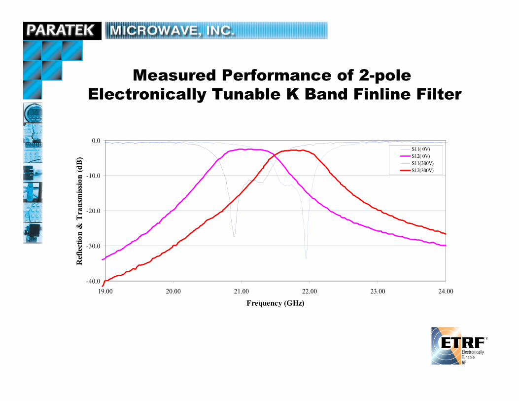
-40.0
-30.0
-20.0
-10.0
0.0
19.00 20.00 21.00 22.00 23.00 24.00
Frequency (GHz)
Ref
lect
ion
& T
rans
miss
ion
(dB
)
S11( 0V)S12( 0V)S11(300V)S12(300V)
Measured Performance of 2-pole Electronically Tunable K Band Finline Filter

Measured Frequency Response of K Band 3-pole Finline Filter
-80
-70
-60
-50
-40
-30
-20
-10
0
20 21 22 23 24 25 26Frequency (GHz)
Ref
lect
ion
& T
rans
mis
sion
(dB
)
S11S12

Phased Array Antenna SystemMain Beam Direction
Radiating Elements
PhaseShifterDriver
Power Combiner/Divider(Feeding System)
Low NoiseAmplifier
High PowerAmplifier
Down Converter Demodulator
ModulatorUpConverter
TrackingSoftware
BeamController
Tracking and Control
Communications Terminal

Phased Array Antenna System------ Key Components using Key Technology
1. Phase Shiftersa) Co-Planar Line Phase Shiftersb) Microstrip Line Phase Shiftersc) Reflect Type Phase Shiftersd) Finline Phase Shifters2. Power Combiner/Dividera) Primary Feeding Horn b) Radial Line Waveguidec) Plane Wave Feeding System
Reflect TypeMulti-layerLens Type

Finline Phase Shifter #2
-120
0
120
240
360
480
0 100 200 300 400
Voltage (V)
Ph
ase S
hif
t (d
eg
ree)
Tested at 30 GHz
Finline Device DataFinline phase shifter #2
0
2
4
6
8
10
12
0 50 100 150 200 250 300 350 400
Voltage (V)
Insert
ion
Lo
ss (
dB
)
Tested at 30 GHz
Insertion loss variation: 3dB/360deg

Coplanar Waveguide Transmission Line Phase Shifter
12.6mm
Floating (capacitivly coupled) RF ground
microstrip CPW

CoplanarPhase-shift vs. Bias Voltage

CoplanarPhase Shifter Insertion Loss

Microstrip Phase-shift vs. Bias Voltage

MicrostripPhase Shifter Insertion Loss

1D Scanning Antenna

• 16 × 16 stacked patch array, consisting of 16 center-series fed linear arrays• V-polarized• 27.5GHz to 28.5 GHz band• Electronically steerable in azimuth ±45° from boresight• Cosecant square shaped beam in elevation, with low upper sidelobes• F/B ratio >30dB • Gain: >22dBi• Max power 10W• VSWR 1.5 : 1• Size : 10 × 12.4cm
1D Scanning Antenna

30 40 50 60 70 80 90 100 110 120 130 140 15040
35
30
25
20
15
10
5
0.
Elevation angle from zenith
Amplitude [dBi]
1D Scanning Antenna Elevation Pattern

Radiating Elements PARATEK Phase Shifters
Connector
Beam Control Lines
Radial LineWaveguide Coupling slots
Or Probes
Beam ControlLines
PARATEK Material Substrate
2D Phased Array Antenna

Antenna Test – Near Field• NSI 3’X 3’ planar near
field range– Complete automation
for production level testing
– All software required for far-field transformation is included with system
– Ability to test antennas in K and Ka Band with easy adaptability for other frequency bands

Antenna Test – Probe Testing• Probe Station and
Universal Test Fixture allows the characterization of coplanar and microstrip components such as phase shifters which may be used in antenna construction
• These tools combined with a vector network analyzer provide electrical performance data essential to the overall performance of the antenna
Sample placed here
RF connectors to network analyzer
RF connectors to network analyzer
Universal Test Fixture Sketch

Antenna Test – G/T Testing• G/T Test configuration allows accurate testing of the system gain over
noise performance of the antenna• Test system is compact and mobile allowing antenna to be tested
outside pointed to the sky• G/T measurement components have been purchased and are awaiting
delivery for initial assembly and checkout
Low Voltage Power SupplyRF cable 6’
Manual Variable Attenuator/s
Amplifier
Spectrum Analyzer
PowerSensor
RF Power Meter
RF cable 3’ RF cable 3’AUT
WG/Coax
WG/Coax
Waveguide Termination
WGSwitch
G/T Measurement Configuration

SummaryParascanTM Materials offer:• Voltage Linearity• Power Handling Capability• Low Loss• High Tunability• Fast Switching Speeds• Multiple Processing Solutions
ParascanTM Components deliver:• Fast Tuning• Low Power Consumption• Choice of Planar and Waveguide• Low Insertion Loss• Power Handling CapabilityParascanTM Antennas offer:• Electronic scanning at a low cost with
high performance

Paratek Microwave, Inc.6935N Oakland Mills RoadColumbia, MD 21045www.paratek.com
…Stay Tuned!…Stay Tuned!…Stay Tuned!…Stay Tuned!