drm046, low power bldc drive for fans using the ... · low power bldc designer reference reference...
TRANSCRIPT
MOTOROLA.COM/SEMICONDUCTORS
M68HC08Microcontrollers
DRM046Rev. 0, 09/2003
Low Power BLDC
Designer Reference
Reference Design
Manual
Drive for Fans usingthe MC68HC908QY4
Fre
esc
ale
Se
mic
on
du
cto
r, I
Freescale Semiconductor, Inc.
For More Information On This Product, Go to: www.freescale.com
nc
...

Fre
esc
ale
Se
mic
on
du
cto
r, I
Freescale Semiconductor, Inc.
For More Information On This Product, Go to: www.freescale.com
nc
...
DRM046 — Rev 0 Designer Reference Manual
MOTOROLA 3
Low Power BLDC Drive for Fans using the MC68HC908QY4 Reference DesignDesigner Reference Manual — Rev 0
by: Radim Visinka, MCSL, Roznov
BLDC Motor Theory by: Pavel Grasblum, MCSL, Roznov
Metrowerks and the Metrowerks logo are registered trademarks of Metrowerks, Inc., a wholly owned subsidiary of Motorola, Inc.
CodeWarrior is a registered trademark of Metrowerks, Inc., a wholly owned subsidiary of Motorola, Inc.
Fre
esc
ale
Se
mic
on
du
cto
r, I
Freescale Semiconductor, Inc.
For More Information On This Product, Go to: www.freescale.com
nc
...

Designer Reference Manual DRM046 — Rev 0
4 MOTOROLA
Fre
esc
ale
Se
mic
on
du
cto
r, I
Freescale Semiconductor, Inc.
For More Information On This Product, Go to: www.freescale.com
nc
...

DRM046 — Rev 0 Designer Reference Manual
MOTOROLA List of Sections 5
Designer Reference Manual — DRM046
List of Sections
Section 1. Introduction . . . . . . . . . . . . . . . . . . . . . . . . . . . 13
Section 2. MC68HC908QY Family Advantages and Features . . . . . . . . . . . . . . . . . . . . . . . . . . . . . . . . . . . . . . . 15
Section 3. BLDC Motor Theory . . . . . . . . . . . . . . . . . . . . 17
Section 4. 3-Phase BLDC Low Voltage Reference Design . . . . . . . . . . . . . . . . . . . . . . . . . . . . . . . . . . . . . . . . 25
Section 5. Hardware Design. . . . . . . . . . . . . . . . . . . . . . . 31
Section 6. Software Design . . . . . . . . . . . . . . . . . . . . . . . 45
Section 7. References. . . . . . . . . . . . . . . . . . . . . . . . . . . . 61
Section 8. Appendix A — Schematics and Parts List . .63
Section 9. Appendix B — System Set-up . . . . . . . . . . . . 71
Fre
esc
ale
Se
mic
on
du
cto
r, I
Freescale Semiconductor, Inc.
For More Information On This Product, Go to: www.freescale.com
nc
...

List of Sections
Designer Reference Manual DRM046 — Rev 0
6 List of Sections MOTOROLA
Fre
esc
ale
Se
mic
on
du
cto
r, I
Freescale Semiconductor, Inc.
For More Information On This Product, Go to: www.freescale.com
nc
...

DRM046 — Rev 0 Designer Reference Manual
MOTOROLA Table of Contents 7
Designer Reference Manual — DRM046
Table of Contents
Section 1. Introduction
Section 2. MC68HC908QY Family Advantages and Features
Section 3. BLDC Motor Theory
3.1 Digital Control of a BLDC Motor . . . . . . . . . . . . . . . . . . . . . . . .18
3.2 Independent Switching of Power Transistors . . . . . . . . . . . . . .19
3.3 Complementary Switching of Power Transistors . . . . . . . . . . .20
3.4 Commutation . . . . . . . . . . . . . . . . . . . . . . . . . . . . . . . . . . . . . .21
Section 4. 3-Phase BLDC Low Voltage Reference Design
4.1 Application Outline . . . . . . . . . . . . . . . . . . . . . . . . . . . . . . . . . .25
4.2 Application Description . . . . . . . . . . . . . . . . . . . . . . . . . . . . . . .26
Section 5. Hardware Design
5.1 Pin-by-Pin Descriptions . . . . . . . . . . . . . . . . . . . . . . . . . . . . . .33
5.2 Detailed Design Description . . . . . . . . . . . . . . . . . . . . . . . . . . .36
Section 6. Software Design
6.1 Data Flow . . . . . . . . . . . . . . . . . . . . . . . . . . . . . . . . . . . . . . . . .45
6.2 Software Implementation . . . . . . . . . . . . . . . . . . . . . . . . . . . . .49
6.3 Application Porting for the Customer Specific BLDC Motor . . .52
6.4 Software Listing . . . . . . . . . . . . . . . . . . . . . . . . . . . . . . . . . . . .57
Fre
esc
ale
Se
mic
on
du
cto
r, I
Freescale Semiconductor, Inc.
For More Information On This Product, Go to: www.freescale.com
nc
...
Table of Contents
Designer Reference Manual DRM046 — Rev 0
8 Table of Contents MOTOROLA
6.5 Microcontroller Memory and Peripheral Usage . . . . . . . . . . . .58
Section 7. References
Section 8. Appendix A — Schematics and Parts List
8.1 Schematics . . . . . . . . . . . . . . . . . . . . . . . . . . . . . . . . . . . . . . . .63
8.2 Parts Lists . . . . . . . . . . . . . . . . . . . . . . . . . . . . . . . . . . . . . . . . .67
Section 9. Appendix B — System Set-up
9.1 Contents . . . . . . . . . . . . . . . . . . . . . . . . . . . . . . . . . . . . . . . . . .71
9.2 Hardware Setup . . . . . . . . . . . . . . . . . . . . . . . . . . . . . . . . . . . .71
9.3 Jumper Settings for Controller Board . . . . . . . . . . . . . . . . . . . .72
9.4 Required Software Tools . . . . . . . . . . . . . . . . . . . . . . . . . . . . .74
9.5 Building and Uploading the Application . . . . . . . . . . . . . . . . . .74
9.6 Executing the Application . . . . . . . . . . . . . . . . . . . . . . . . . . . . .75
Fre
esc
ale
Se
mic
on
du
cto
r, I
Freescale Semiconductor, Inc.
For More Information On This Product, Go to: www.freescale.com
nc
...
DRM046 — Rev 0 Designer Reference Manual
MOTOROLA List of Figures 9
Designer Reference Manual — DRM046
List of Figures
Figure Title Page
1-1 Low Power BLDC Drive for Fan . . . . . . . . . . . . . . . . . . . . . . . .133-1 BLDC Motor - Cross Section . . . . . . . . . . . . . . . . . . . . . . . . . .173-2 Voltage Strokes Applied to the 3-ph BLDC Motor . . . . . . . . . .183-3 3-phase BLDC Power Stage. . . . . . . . . . . . . . . . . . . . . . . . . . .193-4 Independent Switching of Power Transistors . . . . . . . . . . . . . .203-5 Complementary Switching of Power Transistors . . . . . . . . . . .213-6 Stator Flux Vectors at Six-Step Control . . . . . . . . . . . . . . . . . .223-7 Situation Right Before Commutation . . . . . . . . . . . . . . . . . . . .233-8 Situation Right After Commutation . . . . . . . . . . . . . . . . . . . . . .234-1 System Concept . . . . . . . . . . . . . . . . . . . . . . . . . . . . . . . . . . . .275-1 Three-Phase BLDC Drive . . . . . . . . . . . . . . . . . . . . . . . . . . . . .325-2 Block Diagram . . . . . . . . . . . . . . . . . . . . . . . . . . . . . . . . . . . . .335-3 Microcontroller with Logic . . . . . . . . . . . . . . . . . . . . . . . . . . . . .385-4 Hall Sensor Interface . . . . . . . . . . . . . . . . . . . . . . . . . . . . . . . .395-5 User’s Interface. . . . . . . . . . . . . . . . . . . . . . . . . . . . . . . . . . . . .405-6 3-Phase H Bridge (Phase A Shown) . . . . . . . . . . . . . . . . . . . .425-7 Current Sensing - Detail . . . . . . . . . . . . . . . . . . . . . . . . . . . . . .436-1 Algorithm Data Flow . . . . . . . . . . . . . . . . . . . . . . . . . . . . . . . . .466-2 Closed Loop Speed Control . . . . . . . . . . . . . . . . . . . . . . . . . . .486-3 Software Implementation - General Overview . . . . . . . . . . . . .506-4 Stator Flux Vectors with Sectors. . . . . . . . . . . . . . . . . . . . . . . .538-1 Microcontroller with Hall Sensor Input and User’s Interface . . .648-2 Power Stage . . . . . . . . . . . . . . . . . . . . . . . . . . . . . . . . . . . . . . .658-3 Power Supply . . . . . . . . . . . . . . . . . . . . . . . . . . . . . . . . . . . . . .669-1 Setup of the Application with BLDC Motor . . . . . . . . . . . . . . . .729-2 Jumper Reference of BLDC Drive Board . . . . . . . . . . . . . . . . .73
Fre
esc
ale
Se
mic
on
du
cto
r, I
Freescale Semiconductor, Inc.
For More Information On This Product, Go to: www.freescale.com
nc
...

List of Figures
Designer Reference Manual DRM046 — Rev 0
10 List of Figures MOTOROLA
Fre
esc
ale
Se
mic
on
du
cto
r, I
Freescale Semiconductor, Inc.
For More Information On This Product, Go to: www.freescale.com
nc
...
DRM046 — Rev 0 Designer Reference Manual
MOTOROLA List of Tables 11
Designer Reference Manual — DRM046
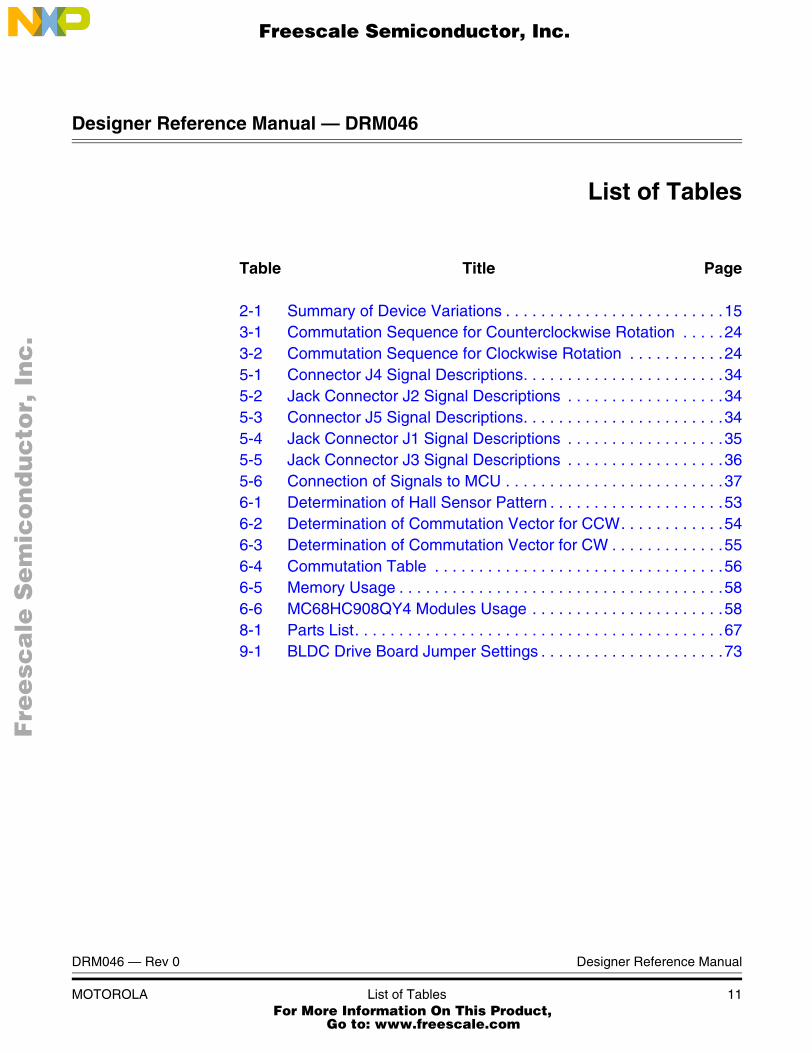
List of Tables
Table Title Page
2-1 Summary of Device Variations . . . . . . . . . . . . . . . . . . . . . . . . .153-1 Commutation Sequence for Counterclockwise Rotation . . . . .243-2 Commutation Sequence for Clockwise Rotation . . . . . . . . . . .245-1 Connector J4 Signal Descriptions. . . . . . . . . . . . . . . . . . . . . . .345-2 Jack Connector J2 Signal Descriptions . . . . . . . . . . . . . . . . . .345-3 Connector J5 Signal Descriptions. . . . . . . . . . . . . . . . . . . . . . .345-4 Jack Connector J1 Signal Descriptions . . . . . . . . . . . . . . . . . .355-5 Jack Connector J3 Signal Descriptions . . . . . . . . . . . . . . . . . .365-6 Connection of Signals to MCU . . . . . . . . . . . . . . . . . . . . . . . . .376-1 Determination of Hall Sensor Pattern . . . . . . . . . . . . . . . . . . . .536-2 Determination of Commutation Vector for CCW. . . . . . . . . . . .546-3 Determination of Commutation Vector for CW . . . . . . . . . . . . .556-4 Commutation Table . . . . . . . . . . . . . . . . . . . . . . . . . . . . . . . . .566-5 Memory Usage . . . . . . . . . . . . . . . . . . . . . . . . . . . . . . . . . . . . .586-6 MC68HC908QY4 Modules Usage . . . . . . . . . . . . . . . . . . . . . .588-1 Parts List. . . . . . . . . . . . . . . . . . . . . . . . . . . . . . . . . . . . . . . . . .679-1 BLDC Drive Board Jumper Settings . . . . . . . . . . . . . . . . . . . . .73
Fre
esc
ale
Se
mic
on
du
cto
r, I
Freescale Semiconductor, Inc.
For More Information On This Product, Go to: www.freescale.com
nc
...

List of Tables
Designer Reference Manual DRM046 — Rev 0
12 List of Tables MOTOROLA
Fre
esc
ale
Se
mic
on
du
cto
r, I
Freescale Semiconductor, Inc.
For More Information On This Product, Go to: www.freescale.com
nc
...
DRM046 — Rev 0 Designer Reference Manual
MOTOROLA Introduction 13
Designer Reference Manual — DRM046
Section 1. Introduction
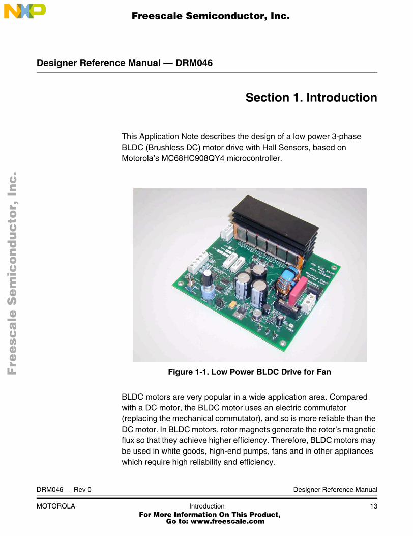
This Application Note describes the design of a low power 3-phase BLDC (Brushless DC) motor drive with Hall Sensors, based on Motorola’s MC68HC908QY4 microcontroller.
Figure 1-1. Low Power BLDC Drive for Fan
BLDC motors are very popular in a wide application area. Compared with a DC motor, the BLDC motor uses an electric commutator (replacing the mechanical commutator), and so is more reliable than the DC motor. In BLDC motors, rotor magnets generate the rotor’s magnetic flux so that they achieve higher efficiency. Therefore, BLDC motors may be used in white goods, high-end pumps, fans and in other appliances which require high reliability and efficiency.
Fre
esc
ale
Se
mic
on
du
cto
r, I
Freescale Semiconductor, Inc.
For More Information On This Product, Go to: www.freescale.com
nc
...

Introduction
Designer Reference Manual DRM046 — Rev 0
14 Introduction MOTOROLA
The concept of the application is a speed-closed loop BLDC drive using a Hall position sensor. It serves as a reference design of a BLDC motor control system for a low voltage fan application. The power stage is designed for 48V DC line voltage and 400W output power. The application is based on the low-cost MC68HC908QY4 “Nitron“ microcontroller. The design is focused on minimal cost and maximal component integration for low cost applications.
This Application Note includes the basic motor theory, system design concept, hardware and software design, hardware schematics, and s/w listing. The design can be used as a reference design for developing customer specific applications.
Fre
esc
ale
Se
mic
on
du
cto
r, I
Freescale Semiconductor, Inc.
For More Information On This Product, Go to: www.freescale.com
nc
...
DRM046 — Rev 0 Designer Reference Manual
MOTOROLA MC68HC908QY Family Advantages and Features 15
Designer Reference Manual — DRM046
Section 2. MC68HC908QY Family Advantages and Features
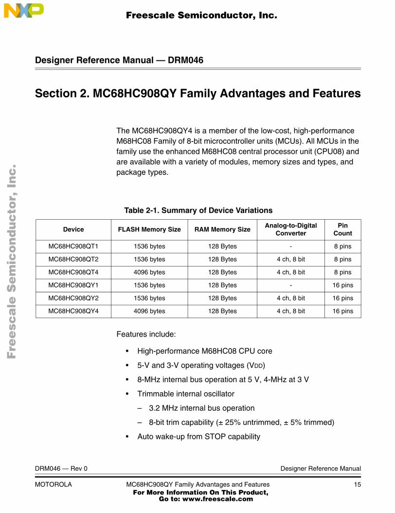
The MC68HC908QY4 is a member of the low-cost, high-performance M68HC08 Family of 8-bit microcontroller units (MCUs). All MCUs in the family use the enhanced M68HC08 central processor unit (CPU08) and are available with a variety of modules, memory sizes and types, and package types.
Features include:
• High-performance M68HC08 CPU core
• 5-V and 3-V operating voltages (VDD)
• 8-MHz internal bus operation at 5 V, 4-MHz at 3 V
• Trimmable internal oscillator
– 3.2 MHz internal bus operation
– 8-bit trim capability (± 25% untrimmed, ± 5% trimmed)
• Auto wake-up from STOP capability
Table 2-1. Summary of Device Variations
Device FLASH Memory Size RAM Memory SizeAnalog-to-Digital
ConverterPin
Count
MC68HC908QT1 1536 bytes 128 Bytes - 8 pins
MC68HC908QT2 1536 bytes 128 Bytes 4 ch, 8 bit 8 pins
MC68HC908QT4 4096 bytes 128 Bytes 4 ch, 8 bit 8 pins
MC68HC908QY1 1536 bytes 128 Bytes - 16 pins
MC68HC908QY2 1536 bytes 128 Bytes 4 ch, 8 bit 16 pins
MC68HC908QY4 4096 bytes 128 Bytes 4 ch, 8 bit 16 pins
Fre
esc
ale
Se
mic
on
du
cto
r, I
Freescale Semiconductor, Inc.
For More Information On This Product, Go to: www.freescale.com
nc
...
MC68HC908QY Family Advantages and Features
Designer Reference Manual DRM046 — Rev 0
16 MC68HC908QY Family Advantages and Features MOTOROLA
• On-chip in-application programmable FLASH memory
• On-chip random-access memory (RAM)
• • 2-channel, 16-bit timer interface module (TIM)
• • 4-channel, 8-bit analog-to-digital converter (ADC) on MC68HC908QY2, MC68HC908QY4, MC68HC908QT2, and MC68HC908QT4
• 5 or 13 bidirectional input/output (I/O) lines, and one input only
• 6-bit keyboard interrupt with walk-up feature (KBI)
• Low-voltage inhibit (LVI) module
• System protection features
• External asynchronous interrupt pin with internal pull-up (IRQ) shared with general-purpose input pin
• Master asynchronous reset pin (RST) shared with general-purpose input/output (I/O) pin
• Power-on reset
• Power saving stop and wait modes
• MC68HC908QY4, MC68HC908QY2, and MC68HC908QY1 are available in these packages:
– 16-pin plastic dual in-line package (PDIP)
– 16-pin small outline integrated circuit (SOIC) package
– 16-pin thin shrink small outline package (TSSOP)
• • MC68HC908QT4, MC68HC908QT2, and MC68HC908QT1 are available in these packages:
– 8-pin PDIP
– 8-pin SOIC
– 8-pin dual flat no lead (DFN) package
The BLDC motor control application requires six PWM outputs, three Hall position sensor inputs and an ADC channel for voltage measurements as a minimum. Therefore 16-pin MC68HC908QY2 or MC68HC908QY4, that accommodate ADC, are the right choice.
Fre
esc
ale
Se
mic
on
du
cto
r, I
Freescale Semiconductor, Inc.
For More Information On This Product, Go to: www.freescale.com
nc
...

DRM046 — Rev 0 Designer Reference Manual
MOTOROLA BLDC Motor Theory 17
Designer Reference Manual — DRM046
Section 3. BLDC Motor Theory
A brushless DC (BLDC) motor is a rotating electric machine where the stator is a classic three-phase stator like that of an induction motor, and the rotor has surface-mounted permanent magnets (see Figure 3-1. BLDC Motor - Cross Section).
In this respect, the BLDC motor is equivalent to a reversed DC commutator motor, in which the magnet rotates while the conductors remain stationary. In the DC commutator motor, the current polarity is altered by the commutator and brushes. On the other hand, in the brushless DC motor, the polarity reversal is performed by power transistors switching in synchronization with the rotor position. Therefore, BLDC motors often incorporate either internal or external position sensors to sense the actual rotor position, or the position can be detected without sensors.
Figure 3-1. BLDC Motor - Cross Section
Stator
Stator winding(in slots)
Shaft
Rotor
Air gap
Permanent magnets
Fre
esc
ale
Se
mic
on
du
cto
r, I
Freescale Semiconductor, Inc.
For More Information On This Product, Go to: www.freescale.com
nc
...
BLDC Motor Theory
Designer Reference Manual DRM046 — Rev 0
18 BLDC Motor Theory MOTOROLA
3.1 Digital Control of a BLDC Motor
The BLDC motor is driven by rectangular voltage strokes coupled with the given rotor position (see Figure 3-2. Voltage Strokes Applied to the 3-ph BLDC Motor). The generated stator flux interacts with the rotor flux, which is generated by a rotor magnet, defines the torque and thus the speed of the motor. The voltage strokes must be properly applied to the two phases of the three-phase winding system so that the angle between the stator flux and the rotor flux is kept close to 90°, to get the maximum generated torque. Due to this fact, the motor requires electronic control for proper operation.
Figure 3-2. Voltage Strokes Applied to the 3-ph BLDC Motor
For the common 3-phase BLDC motor a standard 3-phase power stage is used, as is illustrated in Figure 3-3. 3-phase BLDC Power Stage. The power stage utilizes six power transistors with switching in either the independent mode or complementary mode.
30º 60º 90º 120º 150º 180º 210º 240º 270º 300º 330º Electricalangle
Voltage
Phase A
Phase B
Phase C
+UDCB
-UDCB
+UDCB
-UDCB
+UDCB
-UDCB
Fre
esc
ale
Se
mic
on
du
cto
r, I
Freescale Semiconductor, Inc.
For More Information On This Product, Go to: www.freescale.com
nc
...
BLDC Motor TheoryIndependent Switching of Power Transistors
DRM046 — Rev 0 Designer Reference Manual
MOTOROLA BLDC Motor Theory 19
Figure 3-3. 3-phase BLDC Power Stage
In both modes the 3-phase power stage energizes two motor phases concurrently. The third phase is unpowered (see Figure 3-2. Voltage Strokes Applied to the 3-ph BLDC Motor). Thus, we get six possible voltage vectors that are applied to the BLDC motor using a PWM technique. There are two basic types of power transistor switching: independent switching, and complementary switching.
3.2 Independent Switching of Power Transistors
With independent switching, only two transistors are switched on when current is conducted from the power supply to the phase of the BLDC motor. In one phase, the top transistor is switched on; in the second phase, the bottom transistor is switched on and the third phase is not powered. During freewheeling all transistors are switched off (see Figure 3-4. Independent Switching of Power Transistors).
Q1
PWM_Q5
Q6Q4
C1
Phase_C
PWM_Q1
PWM_Q4
PWM_Q3
Phase_BGND
Q2
UDCB
PWM_Q2
Phase_A
Q3
PWM_Q6
Q5
Fre
esc
ale
Se
mic
on
du
cto
r, I
Freescale Semiconductor, Inc.
For More Information On This Product, Go to: www.freescale.com
nc
...

BLDC Motor Theory
Designer Reference Manual DRM046 — Rev 0
20 BLDC Motor Theory MOTOROLA
Figure 3-4. Independent Switching of Power Transistors
3.3 Complementary Switching of Power Transistors
With complementary switching, two transistors are switched on when the phase of the BLDC motor is connected to the power supply. But there is a difference during freewheeling. With independent switching, all the transistors are switched off. The current continues to flow in the same direction through freewheeling diodes until it falls to zero. Contrary to this, with complementary switching, the complementary transistors are switched on during freewheeling. Thus the current may be able to flow in the opposite direction. Figure 3-5. Complementary Switching of Power Transistors depicts the complementary switching.
10º 20º 30º 40º 50º 60º 70º 80º 90º Electricalangle
PWM Q1
PWM Q2
PWM Q3
PWM Q4
PWM Q5
PWM Q6
PWMswitching
ON
OFFON
OFF
OFF
ON
ON
OFF
OFF
OFF
ON
ON
Fre
esc
ale
Se
mic
on
du
cto
r, I
Freescale Semiconductor, Inc.
For More Information On This Product, Go to: www.freescale.com
nc
...
BLDC Motor TheoryCommutation
DRM046 — Rev 0 Designer Reference Manual
MOTOROLA BLDC Motor Theory 21
.
Figure 3-5. Complementary Switching of Power Transistors
3.4 Commutation
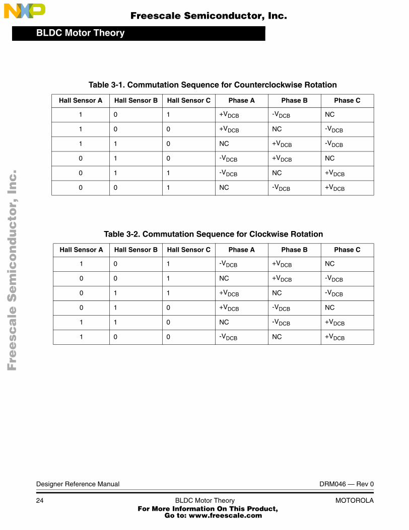
Commutation provides the creation of a rotation field. As was explained, for the proper operation of a BLDC motor it is necessary to keep the angle between the stator and rotor flux close to 90°. With six-step control we get a total of six possible stator flux vectors. The stator flux vector must be changed at a certain rotor position. The rotor position is usually sensed by Hall sensors. The Hall sensors generate three signals that also comprise six states. Each of the Hall sensors’ states corresponds to a certain stator flux vector. All of the Hall sensor states with corresponding stator flux vectors are illustrated in Figure 3-6. Stator Flux Vectors at Six-Step Control. The same figure is illustrated in tables Table 3-1. Commutation Sequence for Counterclockwise Rotation and Table 3-2. Commutation Sequence for Clockwise Rotation.
10º 20º 30º 40º 50º 60º 70º 80º 90º Electricalangle
PWM Q1
PWM Q2
PWM Q3
PWM Q4
PWM Q5
PWM Q6
PWMswitching
ON
OFFON
OFF
OFF
ON
ON
OFF
OFF
OFF
ON
ON
Fre
esc
ale
Se
mic
on
du
cto
r, I
Freescale Semiconductor, Inc.
For More Information On This Product, Go to: www.freescale.com
nc
...
BLDC Motor Theory
Designer Reference Manual DRM046 — Rev 0
22 BLDC Motor Theory MOTOROLA
Figure 3-6. Stator Flux Vectors at Six-Step Control
The next two figures depict the commutation process. The actual rotor position in Figure 3-7. Situation Right Before Commutation corresponds to the Hall sensors’ state ABC[011] (see Figure 3-6. Stator Flux Vectors at Six-Step Control). The actual voltage pattern can be derived from Table 3-1. Commutation Sequence for Counterclockwise Rotation. Phase A is connected to the positive DC-Bus voltage by the transistor Q1; phase C is connected to the ground by transistor Q6, and phase B is unpowered.
As soon as the rotor reaches a certain position (see Figure 3-7. Situation Right Before Commutation) the Hall sensors’ state changes its value from ABC[011] to ABC[010]. From Table 3-1. Commutation Sequence for Counterclockwise Rotation a new voltage pattern is selected and applied to the BLDC motor.
As can be seen, using a six-step control technique, there is no possibility of keeping the angle between the rotor flux and the stator flux precisely at 90°. The real angle varies from 60° to 120°.
Fre
esc
ale
Se
mic
on
du
cto
r, I
Freescale Semiconductor, Inc.
For More Information On This Product, Go to: www.freescale.com
nc
...

BLDC Motor TheoryCommutation
DRM046 — Rev 0 Designer Reference Manual
MOTOROLA BLDC Motor Theory 23
The commutation is repeated per each 60 electrical degrees. The commutation event is critical for its angular (time) accuracy. Any deviation causes the torque ripples and hence speed variation.
Figure 3-7. Situation Right Before Commutation
Figure 3-8. Situation Right After Commutation
Fre
esc
ale
Se
mic
on
du
cto
r, I
Freescale Semiconductor, Inc.
For More Information On This Product, Go to: www.freescale.com
nc
...
BLDC Motor Theory
Designer Reference Manual DRM046 — Rev 0
24 BLDC Motor Theory MOTOROLA
Table 3-1. Commutation Sequence for Counterclockwise Rotation
Hall Sensor A Hall Sensor B Hall Sensor C Phase A Phase B Phase C
1 0 1 +VDCB -VDCB NC
1 0 0 +VDCB NC -VDCB
1 1 0 NC +VDCB -VDCB
0 1 0 -VDCB +VDCB NC
0 1 1 -VDCB NC +VDCB
0 0 1 NC -VDCB +VDCB
Table 3-2. Commutation Sequence for Clockwise Rotation
Hall Sensor A Hall Sensor B Hall Sensor C Phase A Phase B Phase C
1 0 1 -VDCB +VDCB NC
0 0 1 NC +VDCB -VDCB
0 1 1 +VDCB NC -VDCB
0 1 0 +VDCB -VDCB NC
1 1 0 NC -VDCB +VDCB
1 0 0 -VDCB NC +VDCB
Fre
esc
ale
Se
mic
on
du
cto
r, I
Freescale Semiconductor, Inc.
For More Information On This Product, Go to: www.freescale.com
nc
...
DRM046 — Rev 0 Designer Reference Manual
MOTOROLA 3-Phase BLDC Low Voltage Reference Design 25
Designer Reference Manual — DRM046
Section 4. 3-Phase BLDC Low Voltage Reference Design
4.1 Application Outline
The system is designed to drive a 3-phase BLDC motor. The reference design meets the following performance specification:
• Voltage control of BLDC motor using Hall sensors
• Single board solution with MC68HC908QY2/4 “Nitron“ microcontroller
• Power supply voltage +48VDC (range form +36VDC to +56VDC)
• Maximal power 200W (power devices rated for 100V/57A)
• Control technique incorporates:
– Position sensing using Hall sensor signals
– Voltage BLDC motor control with speed-closed loop
– Speed measurement based on Hall Sensors
– One direction of rotation
– Motoring/Generator mode
– Start from any motor position without rotor alignment
– Pre-charging of MOSFET pre-driver bootstraps before each motor start
– Minimal speed 750 RPM (according to the motor used)
– Maximal speed 4000 RPM (according to the motor used)
• Manual interface (run/stop switch, speed potentiometer, power-on LED indication)
• Option to connect user’s interface through terminals
• Fault protection:
– DC-Bus over-current fault protection (hardware/software)
Fre
esc
ale
Se
mic
on
du
cto
r, I
Freescale Semiconductor, Inc.
For More Information On This Product, Go to: www.freescale.com
nc
...
3-Phase BLDC Low Voltage Reference Design
Designer Reference Manual DRM046 — Rev 0
26 3-Phase BLDC Low Voltage Reference Design MOTOROLA
– DC-Bus under-voltage fault protection (software)
– DC-Bus over-voltage fault protection (software)
– Loss of Hall sensors (software)
• Power Supply Accommodation
– Fuse on power line input
– Transient Voltage Suppressor 60 Volts
– Line choke (limited to 8 Amps)
4.2 Application Description
The drive is illustrated in Figure 4-1. System Concept. The system incorporates:
• Single Board BLDC Drive with MC68HC908QY4 “Nitron“ microcontroller
• BLDC Motor with Hall sensors
The MCU MC68HC908QY4 runs the main control algorithm. According to the user interface and feedback signals it generates 3-phase PWM output signals for a 3-phase inverter.
Fre
esc
ale
Se
mic
on
du
cto
r, I
Freescale Semiconductor, Inc.
For More Information On This Product, Go to: www.freescale.com
nc
...

3-Phase BLDC Low Voltage Reference DesignApplication Description
DRM046 — Rev 0 Designer Reference Manual
MOTOROLA 3-Phase BLDC Low Voltage Reference Design 27
Figure 4-1. System Concept
4.2.1 Six-Channel PWM Generation
Six output pins of MC68HC908QY4 are used for control of power MOSFETs. Since the MC68HC908QY4 accommodates just one timer with two timer channels, a general purpose I/O pins needs to be used for the gate signal generation. They are two possibilities of PWM generation using the general purpose I/O pins:
• Use s/w PWM generation on GPIO
• Use external logic with PWM generation using timer of MCU
The first option enables to generate arbitrary PWMs on individual pins. The output compare and overflow ISRs of the on-chip timer can serve as a reference event for the output pin toggle to get the desired PWM pulses. The outputs are controlled purely by s/w. The advantage is the simplicity of the hardware where individual pins are connected directly to
PWMGeneration
SpeedCommand
MC68HC908QY4
Fault Protection
SpeedRamp
Duty Cycle
SpeedProcessing
(Input capture)
SpeedPI
Contr.
-
+
Motor Speed
SpeedError BLDC
State Machine
Commutation Vector
Hall SensorSignals
C
12VDC
5VDC
=
3-phBLDC
48VdcHS
Drivers=
PWM'sDC
-Bus
Vol
tage Gate PWM
FilterCap
NAND Logic
StartStop
SpeedSetup
User Interface
DC-Bus Current
Over-Current Fault
B
A
PWM
Fre
esc
ale
Se
mic
on
du
cto
r, I
Freescale Semiconductor, Inc.
For More Information On This Product, Go to: www.freescale.com
nc
...

3-Phase BLDC Low Voltage Reference Design
Designer Reference Manual DRM046 — Rev 0
28 3-Phase BLDC Low Voltage Reference Design MOTOROLA
3-phase gate driver. The key disadvantages are the considerable fluctuation of PWM duty cycle due to the software interrupt service and interrupts latency; difficulties in getting PWM duty cycles close to 0 and 100% boundaries, due to the necessary software execution, and last but not least, the MCU overloading due to the frequent highest priority PWM interrupts at each PWM edge. As a result the technique has just a limited use.
The second option gives more precise output control signals with the disadvantage of more complex hardware. The PWM is generated by the on-chip timer output compare function, and the general purpose pins serve just to deliver the PWM to the respective input of 3-phase gate driver. Such topology enables controlling the power stage and the BLDC motor in independent unipolar mode, while the same PWM is always present on one top and one bottom switch of two different phases. The other power switches are turned off. The advantages are stable PWM signals, possibility of generating duty cycles from 0 to 100%, and off-loading the MCU. The draw-back is the increased hardware complexity. This topology has been selected for the reference design of BLDC drive.
4.2.2 Control Algorithm Description
The state of the user interface is periodically scanned, while the speed of the motor is measured on each new coming edge from the Hall sensors (only one phase is used for speed measurement). According to the state of the control signals (run/stop switch, speed pot) the speed command is calculated. The acceleration/deceleration ramp is implemented. The comparison between the actual speed command and the measured speed generates a speed error. This speed error is input to the speed PI controller, that generates a new corrected PWM duty cycle.
The Hall sensor signals are scanned independently on a speed control loop. According to the Hall sensor signals the proper commutation vector is selected and applied to the MCU output pins.
The PWM duty cycle value, together with commutation vector, defines the PWM control signals for the BLDC power stage. The PWM is
Fre
esc
ale
Se
mic
on
du
cto
r, I
Freescale Semiconductor, Inc.
For More Information On This Product, Go to: www.freescale.com
nc
...

3-Phase BLDC Low Voltage Reference DesignApplication Description
DRM046 — Rev 0 Designer Reference Manual
MOTOROLA 3-Phase BLDC Low Voltage Reference Design 29
generated by the output compare function on the timer pin, while 6 GPIO pins are set/cleared according to the commutation vector. Six external NAND logic gates provide PWM signals to the MOSFET pre-drivers according to the generated PWM (see Figure 5-3. Microcontroller with Logic).
The bootstrap capacitors of high-side MOSFET drivers require pre-charging before the motor is started. Therefore, all three low-side MOSFETs are turned on for 10msec before each motor start. Such operation enables charging the bootstrap capacitors and a reliable motor start up.
4.2.3 Protection Features
During deceleration the motor can work as a generator. In the generator state, the DC-Bus capacitor is charged and its voltage can easily exceed its maximal voltage. Therefore, the DC-Bus voltage is measured and compared with the limit. Where there is deceleration over-voltage, the deceleration is interrupted and the motor runs with constant speed in order to discharge the DC-Bus capacitor. Then deceleration can continue.
The drive accommodates a fault protection. DC-Bus current is evaluated by hardware and in the case of an over-current, a fault signal is generated. The fault signal is processed by MCU interrupt (IRQ) and software immediately disables the PWM output. DC-Bus voltage is measured during the control process. Where there is over-voltage or under-voltage, the drive enters a fault state. If any of the afore mentioned faults occur, the motor control PWM outputs are disabled in order to protect the drive. The drive can be enabled again using the run/stop switch.
Fre
esc
ale
Se
mic
on
du
cto
r, I
Freescale Semiconductor, Inc.
For More Information On This Product, Go to: www.freescale.com
nc
...

3-Phase BLDC Low Voltage Reference Design
Designer Reference Manual DRM046 — Rev 0
30 3-Phase BLDC Low Voltage Reference Design MOTOROLA
Fre
esc
ale
Se
mic
on
du
cto
r, I
Freescale Semiconductor, Inc.
For More Information On This Product, Go to: www.freescale.com
nc
...
DRM046 — Rev 0 Designer Reference Manual
MOTOROLA Hardware Design 31
Designer Reference Manual — DRM046
Section 5. Hardware Design
The 3-phase BLDC drive is DC 48 volt, 200 watt single board drive controlled by MC68HC908QY4 microcontroller. It provides a ready-to-use reference design as well as a ready-made software development platform for fractional horsepower BLDC motors. Feedback signals from Hall sensors, a typical position sensor used in BLDC motor applications, are provided, - allowing 3-phase BLDC motors to be controlled in closed speed loop.
An illustration of the drive is shown in Figure 5-2. Block Diagram.
Fre
esc
ale
Se
mic
on
du
cto
r, I
Freescale Semiconductor, Inc.
For More Information On This Product, Go to: www.freescale.com
nc
...

Hardware Design
Designer Reference Manual DRM046 — Rev 0
32 Hardware Design MOTOROLA
Figure 5-1. Three-Phase BLDC Drive
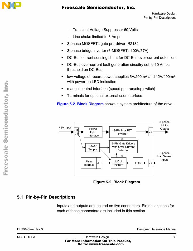
The drive features are:
• on-board microcontroller MC68HC908QY4 with output control logic circuitry
• 3-phase Hall sensor inputs with pull-ups and filters
• Selectable 5VDC and 12VDC available on Hall sensor terminal
• DC input 48VDC with range form +36VDC to +56VDC accommodating:
– Fuse on power line input
Fre
esc
ale
Se
mic
on
du
cto
r, I
Freescale Semiconductor, Inc.
For More Information On This Product, Go to: www.freescale.com
nc
...
Hardware DesignPin-by-Pin Descriptions
DRM046 — Rev 0 Designer Reference Manual
MOTOROLA Hardware Design 33
– Transient Voltage Suppressor 60 Volts
– Line choke limited to 8 Amps
• 3-phase MOSFETs gate pre-driver IR2132
• 3-phase bridge inverter (6-MOSFETs 100V/57A)
• DC-Bus current sensing shunt for DC-Bus over-current detection
• DC-Bus over-current fault generation circuitry set to 10 Amps threshold on DC-Bus
• low-voltage on-board power supplies 5V/200mA and 12V/400mA with power-on LED indication
• manual control interface (speed pot, run/stop switch)
• Terminals for optional external user interface
Figure 5-2. Block Diagram shows a system architecture of the drive.
Figure 5-2. Block Diagram
5.1 Pin-by-Pin Descriptions
Inputs and outputs are located on five connectors. Pin descriptions for each of these connectors are included in this section.
48V Input
User Interface
Power Input
Interface
3-Ph. MosFET Inverter
Power Supply
3-Ph. Gate Drivers with Over-Current
Detection
MCU "Nitron"
3-phaseMotor
Output
3-phaseHall Sensor
InputsFilter
J2J4 J5
J1J3
Fre
esc
ale
Se
mic
on
du
cto
r, I
Freescale Semiconductor, Inc.
For More Information On This Product, Go to: www.freescale.com
nc
...
Hardware Design
Designer Reference Manual DRM046 — Rev 0
34 Hardware Design MOTOROLA
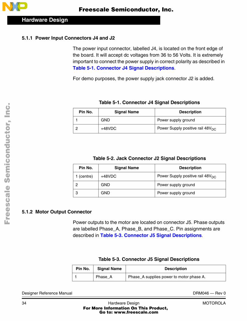
5.1.1 Power Input Connectors J4 and J2
The power input connector, labelled J4, is located on the front edge of the board. It will accept dc voltages from 36 to 56 Volts. It is extremely important to connect the power supply in correct polarity as described in Table 5-1. Connector J4 Signal Descriptions.
For demo purposes, the power supply jack connector J2 is added.
5.1.2 Motor Output Connector
Power outputs to the motor are located on connector J5. Phase outputs are labelled Phase_A, Phase_B, and Phase_C. Pin assignments are described in Table 5-3. Connector J5 Signal Descriptions.
Table 5-1. Connector J4 Signal Descriptions
Pin No. Signal Name Description
1 GND Power supply ground
2 +48VDC Power Supply positive rail 48VDC
Table 5-2. Jack Connector J2 Signal Descriptions
Pin No. Signal Name Description
1 (centre) +48VDC Power Supply positive rail 48VDC
2 GND Power supply ground
3 GND Power supply ground
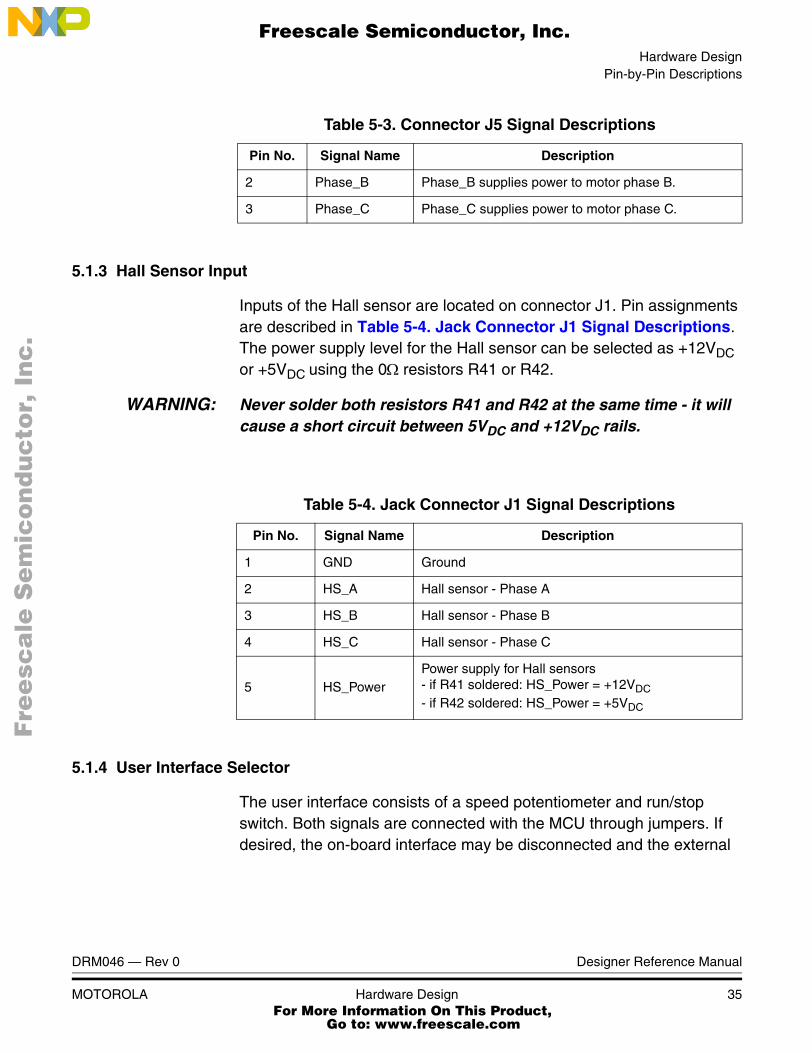
Table 5-3. Connector J5 Signal Descriptions
Pin No. Signal Name Description
1 Phase_A Phase_A supplies power to motor phase A.
Fre
esc
ale
Se
mic
on
du
cto
r, I
Freescale Semiconductor, Inc.
For More Information On This Product, Go to: www.freescale.com
nc
...
Hardware DesignPin-by-Pin Descriptions
DRM046 — Rev 0 Designer Reference Manual
MOTOROLA Hardware Design 35
5.1.3 Hall Sensor Input
Inputs of the Hall sensor are located on connector J1. Pin assignments are described in Table 5-4. Jack Connector J1 Signal Descriptions. The power supply level for the Hall sensor can be selected as +12VDC or +5VDC using the 0Ω resistors R41 or R42.
WARNING: Never solder both resistors R41 and R42 at the same time - it will cause a short circuit between 5VDC and +12VDC rails.
5.1.4 User Interface Selector
The user interface consists of a speed potentiometer and run/stop switch. Both signals are connected with the MCU through jumpers. If desired, the on-board interface may be disconnected and the external
2 Phase_B Phase_B supplies power to motor phase B.
3 Phase_C Phase_C supplies power to motor phase C.
Table 5-3. Connector J5 Signal Descriptions
Pin No. Signal Name Description
Table 5-4. Jack Connector J1 Signal Descriptions
Pin No. Signal Name Description
1 GND Ground
2 HS_A Hall sensor - Phase A
3 HS_B Hall sensor - Phase B
4 HS_C Hall sensor - Phase C
5 HS_PowerPower supply for Hall sensors- if R41 soldered: HS_Power = +12VDC- if R42 soldered: HS_Power = +5VDC
Fre
esc
ale
Se
mic
on
du
cto
r, I
Freescale Semiconductor, Inc.
For More Information On This Product, Go to: www.freescale.com
nc
...
Hardware Design
Designer Reference Manual DRM046 — Rev 0
36 Hardware Design MOTOROLA
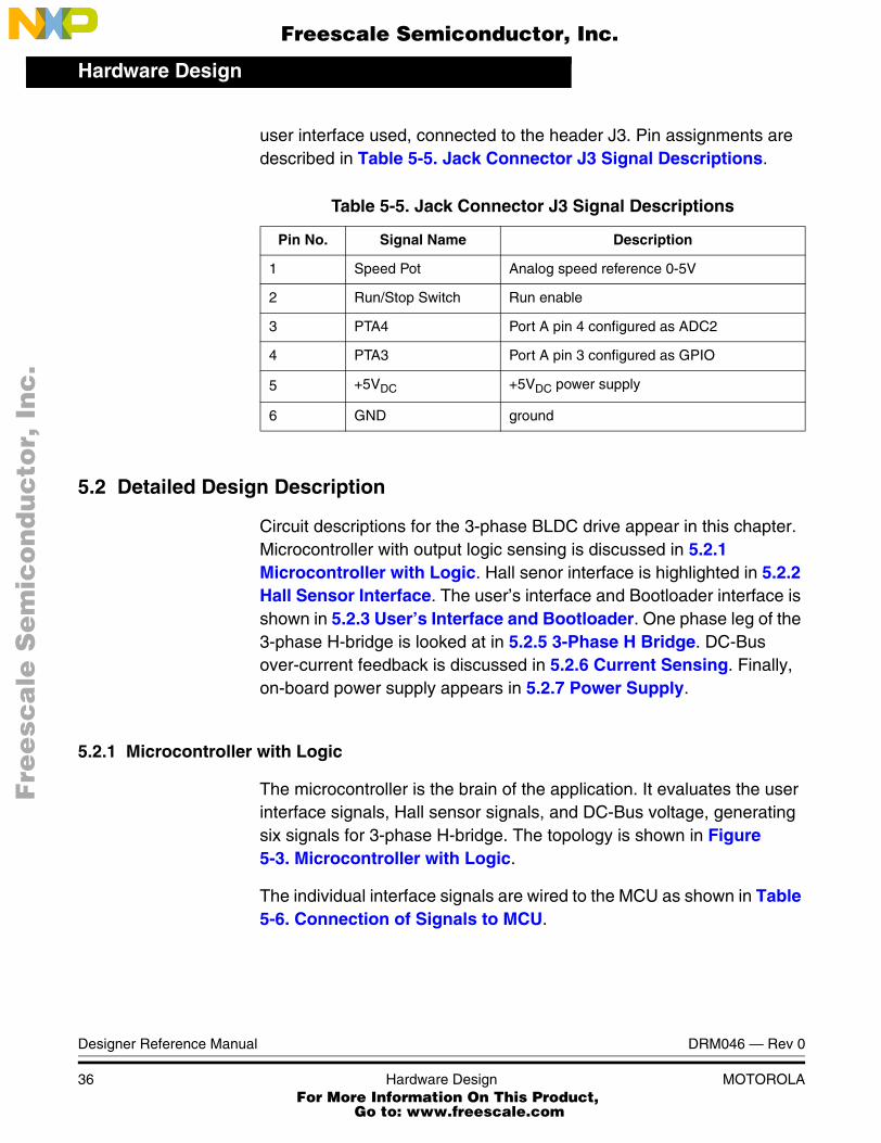
user interface used, connected to the header J3. Pin assignments are described in Table 5-5. Jack Connector J3 Signal Descriptions.
5.2 Detailed Design Description
Circuit descriptions for the 3-phase BLDC drive appear in this chapter. Microcontroller with output logic sensing is discussed in 5.2.1 Microcontroller with Logic. Hall senor interface is highlighted in 5.2.2 Hall Sensor Interface. The user’s interface and Bootloader interface is shown in 5.2.3 User’s Interface and Bootloader. One phase leg of the 3-phase H-bridge is looked at in 5.2.5 3-Phase H Bridge. DC-Bus over-current feedback is discussed in 5.2.6 Current Sensing. Finally, on-board power supply appears in 5.2.7 Power Supply.
5.2.1 Microcontroller with Logic
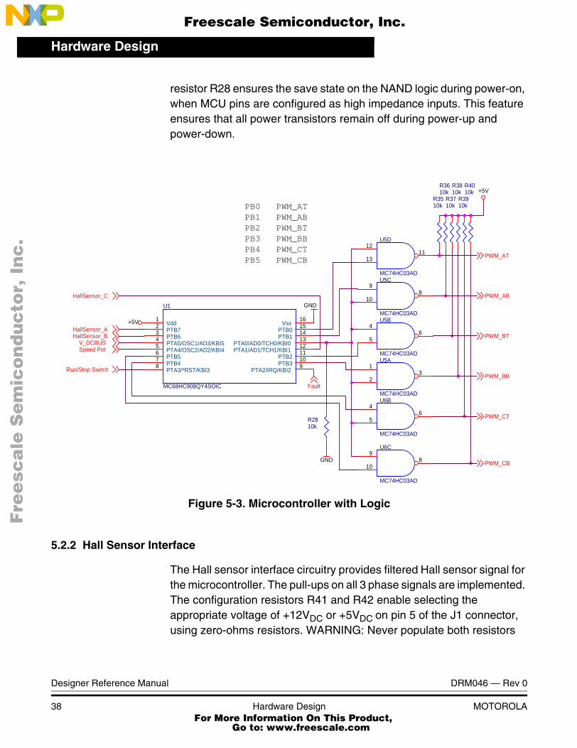
The microcontroller is the brain of the application. It evaluates the user interface signals, Hall sensor signals, and DC-Bus voltage, generating six signals for 3-phase H-bridge. The topology is shown in Figure 5-3. Microcontroller with Logic.
The individual interface signals are wired to the MCU as shown in Table 5-6. Connection of Signals to MCU.
Table 5-5. Jack Connector J3 Signal Descriptions
Pin No. Signal Name Description
1 Speed Pot Analog speed reference 0-5V
2 Run/Stop Switch Run enable
3 PTA4 Port A pin 4 configured as ADC2
4 PTA3 Port A pin 3 configured as GPIO
5 +5VDC +5VDC power supply
6 GND ground
Fre
esc
ale
Se
mic
on
du
cto
r, I
Freescale Semiconductor, Inc.
For More Information On This Product, Go to: www.freescale.com
nc
...

Hardware DesignDetailed Design Description
DRM046 — Rev 0 Designer Reference Manual
MOTOROLA Hardware Design 37
As can be seen, all signals of MC68HC908QY4 are used.
Six outputs, PTB0-PTB5 are used for control of the power MOSFETs. They are wired through NAND’s with open collector and corresponding pull-ups. The PWM is generated on TCH0, and the individual pins PTB0 - PTB5 enable the PWM to appear at the corresponding input of the 3-phase gate driver.
When power is applied or removed, it is important that the top and bottom output transistors in the same phase are not turned on simultaneously. Since logic states are not always defined during power-up, it is important to ensure that all power transistors remain off when the controller’s supply voltage is below its normal operating level. Since the inputs of the 3-phase gate driver IR2132 have negative logic, the pull-up resistors R35-R40 disable the driver outputs. Also, pull down
Table 5-6. Connection of Signals to MCU
Signal MC6+8HC908QY4 Pins
Hall Sensor A PTB7
Hall Sensor B PTB6
Hall Sensor C PTA1 / TCH1
Phase A Top PTB0
Phase A Bottom PTB1
Phase B Top PTB2
Phase A Bottom PTB3
Phase C Top PTB4
Phase C Bottom PTB5
PWM / Enable PTA0 / TCH0
Fault Input PTA2 / IRQ
DC-Bus Voltage PTA5 / AD3
Speed Pot PTA4 / AD2
Run / Stop Switch PTA3
Fre
esc
ale
Se
mic
on
du
cto
r, I
Freescale Semiconductor, Inc.
For More Information On This Product, Go to: www.freescale.com
nc
...
Hardware Design
Designer Reference Manual DRM046 — Rev 0
38 Hardware Design MOTOROLA
resistor R28 ensures the save state on the NAND logic during power-on, when MCU pins are configured as high impedance inputs. This feature ensures that all power transistors remain off during power-up and power-down.
Figure 5-3. Microcontroller with Logic
5.2.2 Hall Sensor Interface
The Hall sensor interface circuitry provides filtered Hall sensor signal for the microcontroller. The pull-ups on all 3 phase signals are implemented. The configuration resistors R41 and R42 enable selecting the appropriate voltage of +12VDC or +5VDC on pin 5 of the J1 connector, using zero-ohms resistors. WARNING: Never populate both resistors
R3510k
R3610k
R3710k
R3810k
R3910k
R4010k +5V
PB0 PWM_ATPB1 PWM_ABPB2 PWM_BTPB3 PWM_BBPB4 PWM_CTPB5 PWM_CB
HallSensor_AHallSensor_B
HallSensor_C
Speed Pot
Run/Stop Switch
+5V
GND
U5C
MC74HC03AD
9
108
U5B
MC74HC03AD
4
56
U5D
MC74HC03AD
12
1311
U5A
MC74HC03AD
1
23
U6B
MC74HC03AD
4
56
U6C
MC74HC03AD
9
108
V_DCBUS
PWM_AT
PWM_BT
PWM_CB
PWM_BB
PWM_CTR2810k
GND
Fault
U1
MC68HC908QY4SOIC
Vdd1
PTB72
PTB63
PTA5/OSC1/AD3/KBI54
PTA4/OSC2/AD2/KBI45
PTB56
PTA3/*RST/KBI38 PTB47
PTA2/IRQ/KBI2 9PTB3 10PTB2 11PTA1/AD1/TCH1/KBI1 12PTA0/AD0/TCH0/KBI0 13PTB1 14PTB0 15Vss 16
PWM_AB
Fre
esc
ale
Se
mic
on
du
cto
r, I
Freescale Semiconductor, Inc.
For More Information On This Product, Go to: www.freescale.com
nc
...

Hardware DesignDetailed Design Description
DRM046 — Rev 0 Designer Reference Manual
MOTOROLA Hardware Design 39
R41 and R42! This causes a short circuit between +12VDC and +5VDCrails.
For brushless motors that use Hall sensor inputs for commutation, noise immunity of the sensor inputs is a key design consideration. Noise on these inputs can be particularly troublesome, since commutation to the wrong state precludes smooth operation of the motor. To facilitate noise, the sensor inputs are filtered with 1000-nsec single-pole filters, as shown in Figure 5-4. Hall Sensor Interface. Using relatively low value pull-up resistors, in the order of 1 kΩ., provides an additional measure of noise immunity.
Figure 5-4. Hall Sensor Interface
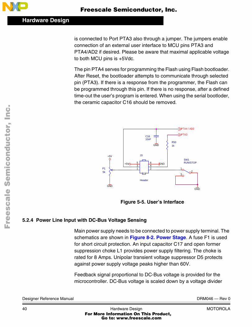
5.2.3 User’s Interface and Bootloader
The user interface enables controlling the drive. It is shown in Figure 5-5. User’s Interface. The speed can be set-up using a potentiometer, - connected through a jumper to channel AD2 of the ADC. A small ceramic capacitor C16 is inserted for signal filtering. The run/stop switch
+12V
GND
GND
+5V
R11k
+5V
R21k
R51k
+5V
+C12u2/20V
C2100nF
C54n7
C64n7
C74n7
R3 220R
R4 220R
R6 220R
GND+5V
R41 0R
R42 0R
J1
12345
HS_A
HS_CHS_B
Hall SensorsConnector
PTA1
PTB6
PTB7
Fre
esc
ale
Se
mic
on
du
cto
r, I
Freescale Semiconductor, Inc.
For More Information On This Product, Go to: www.freescale.com
nc
...
Hardware Design
Designer Reference Manual DRM046 — Rev 0
40 Hardware Design MOTOROLA
is connected to Port PTA3 also through a jumper. The jumpers enable connection of an external user interface to MCU pins PTA3 and PTA4/AD2 if desired. Please be aware that maximal applicable voltage to both MCU pins is +5Vdc.
The pin PTA4 serves for programming the Flash using Flash bootloader. After Reset, the bootloader attempts to communicate through selected pin (PTA3). If there is a response from the programmer, the Flash can be programmed through this pin. If there is no response, after a defined time-out the user’s program is entered. When using the serial bootloder, the ceramic capacitor C16 should be removed.
Figure 5-5. User’s Interface
5.2.4 Power Line Input with DC-Bus Voltage Sensing
Main power supply needs to be connected to power supply terminal. The schematics are shown in Figure 8-2. Power Stage. A fuse F1 is used for short circuit protection. An input capacitor C17 and open former suppression choke L1 provides power supply filtering. The choke is rated for 8 Amps. Unipolar transient voltage suppressor D5 protects against power supply voltage peaks higher than 60V.
Feedback signal proportional to DC-Bus voltage is provided for the microcontroller. DC-Bus voltage is scaled down by a voltage divider
R501k
J3
Header
246
135
GND
P15k
+5V
GND
+5V GNDSW1RUN/STOP
21
3
PTA3
PTA4 / AD2
C1610nF
GND
Fre
esc
ale
Se
mic
on
du
cto
r, I
Freescale Semiconductor, Inc.
For More Information On This Product, Go to: www.freescale.com
nc
...

Hardware DesignDetailed Design Description
DRM046 — Rev 0 Designer Reference Manual
MOTOROLA Hardware Design 41
consisting of R11 and R12. The values are chosen such that a 65-volt maximum DC-Bus voltage corresponds to 5 volts at output V_DCBUS.
5.2.5 3-Phase H Bridge
The output stage is configured as a 3-phase H-bridge with IGBT output transistors. It is simplified considerably by a high-voltage integrated 3-phase gate driver that has a cycle-by-cycle current limit feature with over-current detection and fault generation. A schematic that shows one phase is illustrated in Figure 5-6. 3-Phase H Bridge (Phase A Shown).
Gate drive is supplied by an International Rectifier, IR2132. It is a high voltage, high speed power MOSFET and IGBT driver with three independent high and low side referenced output channels. Under-voltage lockout and over-current protection are also provided by the IR2132.
One of the more important design decisions in a motor drive is the selection of gate drive impedance for the output transistors. In Figure 5-6. 3-Phase H Bridge (Phase A Shown), resistor R16, resistor R30, diode D8, and the IR2132’s current source/sinking capability determine gate drive impedance for the lower half-bridge transistor. A similar network is used on the upper half-bridge. These networks set turn-on gate drive impedance at approximately 24 ohms and turn-off gate impedance to approximately 4 ohms. These values produce transition times of approximately 200 nsec.
The gate of the MOSFETs is protected by 18V Zener diodes D18 and D21 that eliminate possible dangerous peaks on the gate signals. Discharge resistors R44 and R47 are placed in parallel.
Fre
esc
ale
Se
mic
on
du
cto
r, I
Freescale Semiconductor, Inc.
For More Information On This Product, Go to: www.freescale.com
nc
...

Hardware Design
Designer Reference Manual DRM046 — Rev 0
42 Hardware Design MOTOROLA
Figure 5-6. 3-Phase H Bridge (Phase A Shown)
5.2.6 Current Sensing
As mentioned, the 3-phase driver IR2132 contains cycle-by-cycle current limit feature with over-current detection and fault generation. An on-chip ground-referenced operational amplifier provides analog feedback of bridge current via an external current sense resistor. A current trip function, which terminates all six outputs is also derived from this resistor. An open drain /FAULT signal indicates if an over-current or under-voltage shutdown has occurred.
Figure 5-7. Current Sensing - Detail illustrates the detailed topology of the circuitry derived from Figure 5-6. 3-Phase H Bridge (Phase A Shown). Both operational amplifier and comparator are available within IR2132, so just resistors R21 and R22 are needed externally. The resistors R21 and R22 define the gain of the on-chip operational amplifier. The gain is set to -10. The over-current trip is set internally to 0.5V. It corresponds to 10A for DC-Bus sensing resistor 0.005 ohms and
Motor Ph A
GND
Phase COutput
Phase BOutput
Phase C Input
Phase B Input
R430R C36
GND
+12V
C21470nF/25V
C25100nF
R1524R
R1624R
Fault
+12V
Optional filter
GND
+12V
D7MURS160T3
+
C24100uF/25V
C35100nF
DC Bus cureentsensing resistors
U2
IR2132S
HIN23
LIN26
HIN34
LIN37
HIN12
LIN15
FAULT8
ITRIP9
CA010
CA-11
VCC1
VSS12
VS1 26HO1 27VB1 28
LO1 16
LO2 15
LO3 14
HO2 23
HO3 19
VB2 24
VB3 20
VS2 22
VS3 18
VS013
D6MBRS240LT3
D8MBRS240LT3
PWM_ATPWM_AB
R2182k - 1%
R228k2 - 1%
GND
R294R7
R304R7
0.5V @ (Imax=10A)
R140R010 - SBL4
R130R010 - SBL4
D18MMSZ5248BT1
R4447k
D21MMSZ5248BT1
R4747k
Q1IRF3710
+48V
Q4IRF3710
Fre
esc
ale
Se
mic
on
du
cto
r, I
Freescale Semiconductor, Inc.
For More Information On This Product, Go to: www.freescale.com
nc
...

Hardware DesignDetailed Design Description
DRM046 — Rev 0 Designer Reference Manual
MOTOROLA Hardware Design 43
gain -10. The optional filter (C36/R43) at the output of the operational amplifier, helps to filter undesirable noise. If not used, 0 ohms resistor R43 will be inserted.
Where there is over-current, all six gate driver outputs are disabled, and a fault is generated. Since the generated fault signal is an open collector output, the internal pull-up of MC68HC908QY4 is utilized.
Figure 5-7. Current Sensing - Detail
5.2.7 Power Supply
On-board power supply provides auxiliary +5Vdc and +12Vdc. The topology is shown in Figure 8-3. Power Supply. The input voltage (in range from +36Vdc to +56Vdc) is decreased to +12V by a switched mode DC-DC converter LT1676. It accepts input voltage up to +60Vdc. The +12Vdc is used for supplying the 3-phase gate driver and optionally for supplying of the Hall position sensor. The +12Vdc power supply is rated to 400mA.
The +12Vdc is further decreased by linear regulator MC78M05 giving +5Vdc. The +5Vdc is used for supplying the microcontroller, user
R230R
GND
C37
Optional filterR2182k - 1%
R228k2 - 1%
GND
+
-
Amplifier
+
-
Comparator
+0.5V
R140R010 - SBL4
R130R010 - SBL4
GND
power groundtrack of thepower stage
0.5V @(Imax=10A)
Fault
IR2132
ITRIP
CA-CAO
/FAULT
VC0
Fre
esc
ale
Se
mic
on
du
cto
r, I
Freescale Semiconductor, Inc.
For More Information On This Product, Go to: www.freescale.com
nc
...

Hardware Design
Designer Reference Manual DRM046 — Rev 0
44 Hardware Design MOTOROLA
interface, logic, and optionally, the Hall position sensors. The +5Vdc power supply is rated to 400mA.
Fre
esc
ale
Se
mic
on
du
cto
r, I
Freescale Semiconductor, Inc.
For More Information On This Product, Go to: www.freescale.com
nc
...

DRM046 — Rev 0 Designer Reference Manual
MOTOROLA Software Design 45
Designer Reference Manual — DRM046
Section 6. Software Design
This section describes the design of the software blocks of the drive. The software will be described in terms of -
• Control Algorithm Data Flow
• Software Implementation
• Software Listing
• Microcontroller Memory and Peripheral Usage
6.1 Data Flow
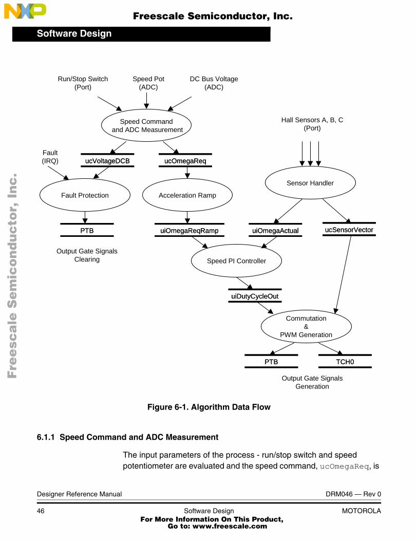
The requirements of the drive dictate that software takes some values from the user interface and sensors, processes them and generates 3-phase PWM signals for motor control.
The control algorithm of closed loop BLDC drive is described in Figure 6-1. Algorithm Data Flow. It consists of processes described in following sub-sections.
Fre
esc
ale
Se
mic
on
du
cto
r, I
Freescale Semiconductor, Inc.
For More Information On This Product, Go to: www.freescale.com
nc
...
Software Design
Designer Reference Manual DRM046 — Rev 0
46 Software Design MOTOROLA
Figure 6-1. Algorithm Data Flow
6.1.1 Speed Command and ADC Measurement
The input parameters of the process - run/stop switch and speed potentiometer are evaluated and the speed command, ucOmegaReq, is
Speed Commandand ADC Measurement
Sensor Handler
ucSensorVectorucSensorVector
ucVoltageDCBucVoltageDCB ucOmegaRequcOmegaReq
Hall Sensors A, B, C(Port)
Run/Stop Switch(Port)
Speed Pot(ADC)
DC Bus Voltage(ADC)
Acceleration Ramp
uiOmegaReqRampuiOmegaReqRamp
Commutation&
PWM Generation
PTBPTB
TCH0TCH0
Speed PI Controller
uiDutyCycleOutuiDutyCycleOut
uiOmegaActualuiOmegaActual
Fault Protection
Fault(IRQ)
PTBPTB
Output Gate Signals Generation
Output Gate Signals Clearing
Fre
esc
ale
Se
mic
on
du
cto
r, I
Freescale Semiconductor, Inc.
For More Information On This Product, Go to: www.freescale.com
nc
...
Software DesignData Flow
DRM046 — Rev 0 Designer Reference Manual
MOTOROLA Software Design 47
calculated accordingly. Also the DC bus voltage, ucVoltageDCB, is measured.
6.1.2 Sensor Handler
The application utilizes 3-phase Hall position sensor for control algorithm. It is used for both commutation vector generation and for the actual speed calculation.
For the calculation of the commutation vector, all three Hall sensor inputs are evaluated. A three-bit commutation pattern, ucSensorVector, is created. It is later used for selection of proper commutation pattern in process Commutation & PWM Generation.
The speed measurement utilizes the IC function of the timer. It reads the time between consequential rising edges of the selected phase of Hall sensor output, and calculates the actual motor speed, uiOmegaActual. Also, a software filter of the speed measurement may be incorporated into the process for better noise immunity. In this case the actual motor speed is calculated as an average value of several measurements.
6.1.3 Acceleration Ramp
The process calculates the new speed command, uiOmegaReqRamp, based on the required speed, ucOmegaReq, according to the acceleration ramp.
During deceleration the motor can work as a generator. In the generator state the DC-Bus capacitor is charged and its voltage can easily exceed its maximal voltage. Therefore the DC-Bus voltage is measured and compared with the limit. In the case of deceleration over-voltage, the deceleration is interrupted and the motor runs with constant speed in order to discharge the capacitor. Then deceleration can continue.
Fre
esc
ale
Se
mic
on
du
cto
r, I
Freescale Semiconductor, Inc.
For More Information On This Product, Go to: www.freescale.com
nc
...
Software Design
Designer Reference Manual DRM046 — Rev 0
48 Software Design MOTOROLA
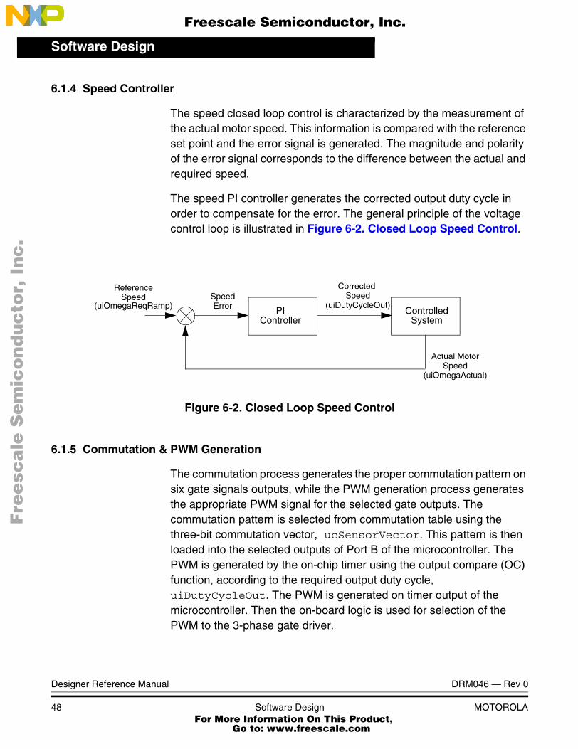
6.1.4 Speed Controller
The speed closed loop control is characterized by the measurement of the actual motor speed. This information is compared with the reference set point and the error signal is generated. The magnitude and polarity of the error signal corresponds to the difference between the actual and required speed.
The speed PI controller generates the corrected output duty cycle in order to compensate for the error. The general principle of the voltage control loop is illustrated in Figure 6-2. Closed Loop Speed Control.
Figure 6-2. Closed Loop Speed Control
6.1.5 Commutation & PWM Generation
The commutation process generates the proper commutation pattern on six gate signals outputs, while the PWM generation process generates the appropriate PWM signal for the selected gate outputs. The commutation pattern is selected from commutation table using the three-bit commutation vector, ucSensorVector. This pattern is then loaded into the selected outputs of Port B of the microcontroller. The PWM is generated by the on-chip timer using the output compare (OC) function, according to the required output duty cycle, uiDutyCycleOut. The PWM is generated on timer output of the microcontroller. Then the on-board logic is used for selection of the PWM to the 3-phase gate driver.
PIController
ControlledSystem
SpeedError
ReferenceSpeed
Corrected Speed
(uiDutyCycleOut)(uiOmegaReqRamp)
Actual MotorSpeed
(uiOmegaActual)
Fre
esc
ale
Se
mic
on
du
cto
r, I
Freescale Semiconductor, Inc.
For More Information On This Product, Go to: www.freescale.com
nc
...

Software DesignSoftware Implementation
DRM046 — Rev 0 Designer Reference Manual
MOTOROLA Software Design 49
6.1.6 Fault Protection
This process is responsible for fault handling. The software accommodates two fault inputs: DC-Bus over-current signal and DC-Bus voltage measurement.
DC-Bus over-current is detected by on-board hardware circuitry. In the case of an over-current, the external hardware provides a falling edge on the /IRQ input of the microcontroller. This signal invokes a non-masked interrupt with highest priority. The interrupt service routine puts all PWM gate signals into a non-active safe state, and sets the fault status of the drive.
DC-Bus voltage is used for software under-voltage and over-voltage protection. The sensed DC-Bus voltage is compared with the limit within the software. In the case of a detected fault, the service routine puts all PWM gate signals into a non-active safe state, and sets the fault status of the drive.
If any of the faults occurs the service routine puts the drive into a safe fault state that does not enable the drive operation. It can be left by turning the run/stop switch to the stop position.
6.2 Software Implementation
The general software implementation is illustrated in Figure 6-3. Software Implementation - General Overview. It incorporates the main routine entered from Reset and three interrupt states. The Main Routine includes the initialization of the microcontroller and the application, and a Software Timer for the control algorithm time base. The interrupt states provides calculation of actual speed of the motor, fault handler and PWM generation process with motor commutation.
Fre
esc
ale
Se
mic
on
du
cto
r, I
Freescale Semiconductor, Inc.
For More Information On This Product, Go to: www.freescale.com
nc
...

Software Design
Designer Reference Manual DRM046 — Rev 0
50 Software Design MOTOROLA
Figure 6-3. Software Implementation - General Overview
6.2.1 Initialization
The Main Routine provides initialization of the microcontroller:
• initializes MCU core
– enables IRQ interrupt, enable IRQ pull-up
• COP and LVI enable (CONFIG register)
• disable KeyBoard interrupts
• sets-up I/O ports
OverFlow Interrupt of Timer 0
Over-flowInterrupt Handler
Input Capture Interrupt of Timer 1
Input CaptureInterrupt Handler done
done
MCU & ApplicationInitialization
SoftwareTimer Timeout
RESET
Timeout
done
IRQ Interrupt
FaultInterrupt Handler
done
done
Fre
esc
ale
Se
mic
on
du
cto
r, I
Freescale Semiconductor, Inc.
For More Information On This Product, Go to: www.freescale.com
nc
...
Software DesignSoftware Implementation
DRM046 — Rev 0 Designer Reference Manual
MOTOROLA Software Design 51
• initializes Timer 0 for Output Compare (OC)
• initializes Timer 1 for Input Capture (IC)
• initializes Analog to Digital Converter
The MCU has just one 16-bit timer counter with two timer channels. The counter is primarily used for the generation of PWM signal of desired period. The duty cycle is defined by timer channel 0 set as an output compare. Channel 1 is used for the speed measurements using the input capture function. It measures the time between the edges of the Hall sensor signal.
After MCU initialization application, variables are initialized and the interrupts are enabled.
6.2.2 Interrupts
The interrupt handlers provide the following services:
• OverFlow Interrupt Handler is used for update of PWM duty cycle and determination of the commutation vector based on the Hall sensor signals (Process Commutation and PWM generation).
• Input Capture (IC) Interrupt Handler reads the time between the two consequential IC edges (basic part of the Process Speed Sensor). Since the only timer of the MCU is used for PWM generation, the determination of time between the Hall sensor edges is based on the number of PWM periods.
• Fault Interrupt Handler takes care of over-current fault interrupt (over-current part of the Process Fault Control)
6.2.3 Software Timer
The software timer routine provides the timing sequence for required subroutines running in the background. The background routine is called in 10msec time-out. The timing is based on counting of the PWM periods.
The background routine provides:
Fre
esc
ale
Se
mic
on
du
cto
r, I
Freescale Semiconductor, Inc.
For More Information On This Product, Go to: www.freescale.com
nc
...

Software Design
Designer Reference Manual DRM046 — Rev 0
52 Software Design MOTOROLA
• Service of Analog-to-Digital Converter for DC-Bus voltage and speed pot measurements
• Determination of desired speed based on application state machine (Stop, Charging, Run, Fault)
• Calculation of the speed command based on speed ramp with DC-Bus over-voltage protection during deceleration
• Calculation of the desired duty cycle using speed PI controller.
6.3 Application Porting for the Customer Specific BLDC Motor
The definition of the correct commutation table is the key point of the application porting for the customer specific BLDC motor. The aim of the process is the definition of the commutation pattern that is generated at the MCU ports according to the sensed Hall sensor pattern. The process of definition has the following steps:
1. Determination of Hall sensor pattern for each commutation sector
2. Determination of commutation vector for each Hall sensor pattern
3. Determination of commutation table according to the s/w implementation
6.3.1 Determination of Hall Sensor Pattern
First, the Hall sensor pattern corresponding to the BLDC motor sector needs to be determined. The determination can be done by supplying all three phases, by combination of positive and negative voltage, that cause the motor to move to the given sector, and observing the Hall sensor signals when the motor settles. Table 6-1. illustrates the required phases to be powered for the desired sector and the example of sensor output for the given BLDC motor. The sectors I - VI correspond with the sectors shown in Figure 6-4. Stator Flux Vectors with Sectors.
Fre
esc
ale
Se
mic
on
du
cto
r, I
Freescale Semiconductor, Inc.
For More Information On This Product, Go to: www.freescale.com
nc
...

Software DesignApplication Porting for the Customer Specific BLDC Motor
DRM046 — Rev 0 Designer Reference Manual
MOTOROLA Software Design 53
Figure 6-4. Stator Flux Vectors with Sectors
6.3.2 Determination of Commutation Vector
When the Hall sensor patterns are defined, the corresponding commutation vectors shall be determined. For each sector I-VI, the corresponding commutation vector A-F and Hall sensor pattern is
Table 6-1. Determination of Hall Sensor Pattern
Sector Powered Phases Sensor Output of the Motor
Phase A Phase B Phase C Hall A Hall B Hall C
I -U -U +U 1 0 1
II -U +U +U 0 0 1
III -U +U -U 0 1 1
IV +U +U -U 0 1 0
V +U -U -U 1 1 0
VI +U -U +U 1 0 0
II
III
VI V VI
I
Fre
esc
ale
Se
mic
on
du
cto
r, I
Freescale Semiconductor, Inc.
For More Information On This Product, Go to: www.freescale.com
nc
...
Software Design
Designer Reference Manual DRM046 — Rev 0
54 Software Design MOTOROLA
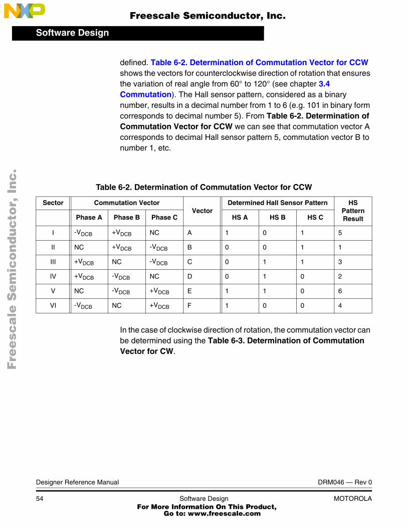
defined. Table 6-2. Determination of Commutation Vector for CCW shows the vectors for counterclockwise direction of rotation that ensures the variation of real angle from 60° to 120° (see chapter 3.4 Commutation). The Hall sensor pattern, considered as a binary number, results in a decimal number from 1 to 6 (e.g. 101 in binary form corresponds to decimal number 5). From Table 6-2. Determination of Commutation Vector for CCW we can see that commutation vector A corresponds to decimal Hall sensor pattern 5, commutation vector B to number 1, etc.
In the case of clockwise direction of rotation, the commutation vector can be determined using the Table 6-3. Determination of Commutation Vector for CW.
Table 6-2. Determination of Commutation Vector for CCW
Sector Commutation VectorVector
Determined Hall Sensor Pattern HS Pattern ResultPhase A Phase B Phase C HS A HS B HS C
I -VDCB +VDCB NC A 1 0 1 5
II NC +VDCB -VDCB B 0 0 1 1
III +VDCB NC -VDCB C 0 1 1 3
IV +VDCB -VDCB NC D 0 1 0 2
V NC -VDCB +VDCB E 1 1 0 6
VI -VDCB NC +VDCB F 1 0 0 4
Fre
esc
ale
Se
mic
on
du
cto
r, I
Freescale Semiconductor, Inc.
For More Information On This Product, Go to: www.freescale.com
nc
...

Software DesignApplication Porting for the Customer Specific BLDC Motor
DRM046 — Rev 0 Designer Reference Manual
MOTOROLA Software Design 55
6.3.3 Determination of Commutation Table
In the application software, the commutation vectors are defined in a table of 8 values (entry 0-7). Any Hall sensor pattern gives the right pointer to the table of commutation vectors. For our example, the commutation table shown in Table 6-4. Commutation Table shall be used. Please note that Hall sensor pattern 0 [000] and 7 [111] indicates a fault, since such a combination is not available during normal operation. Such a state can be caused, e.g. by a disconnected Hall sensor interface, or it’s malfunction. In that case, the output channels are switched off (output signals are put into a safe state) in order to protect the drive.
Table 6-3. Determination of Commutation Vector for CW
Sector Commutation VectorVector
Determined Hall Sensor Pattern HS Pattern ResultPhase A Phase B Phase C HS A HS B HS C
I +VDCB -VDCB NC D 1 0 1 5
II +VDCB NC -VDCB C 1 0 0 4
III NC +VDCB -VDCB B 1 1 0 6
IV -VDCB +VDCB NC A 0 1 0 2
V -VDCB NC +VDCB F 0 1 1 3
VI NC -VDCB +VDCB E 0 0 1 1
Fre
esc
ale
Se
mic
on
du
cto
r, I
Freescale Semiconductor, Inc.
For More Information On This Product, Go to: www.freescale.com
nc
...

Software Design
Designer Reference Manual DRM046 — Rev 0
56 Software Design MOTOROLA
The s/w implementation for counter-clockwise direction of rotation of the above mentioned commutation table is described below:
const unsigned char BLDC_COMMUTATION_TABLE_CCW[8] = TURN_OFF , /* turn-off */VECTOR_B ,VECTOR_D ,VECTOR_C ,VECTOR_F ,VECTOR_A ,VECTOR_E ,TURN_OFF /* turn-off */;
where:
#define TURN_OFF 0x00#define VECTOR_A 0x06#define VECTOR_B 0x24#define VECTOR_C 0x21#define VECTOR_D 0x09#define VECTOR_E 0x18#define VECTOR_F 0x12
The output vector is then generated on port using command:
Table 6-4. Commutation Table
HS Pattern ResultCommutation Vector
CCWCommutation Vector
CW
0 OFF OFF
1 B E
2 D A
3 C F
4 F C
5 A D
6 E B
7 OFF OFF
Fre
esc
ale
Se
mic
on
du
cto
r, I
Freescale Semiconductor, Inc.
For More Information On This Product, Go to: www.freescale.com
nc
...
Software DesignSoftware Listing
DRM046 — Rev 0 Designer Reference Manual
MOTOROLA Software Design 57
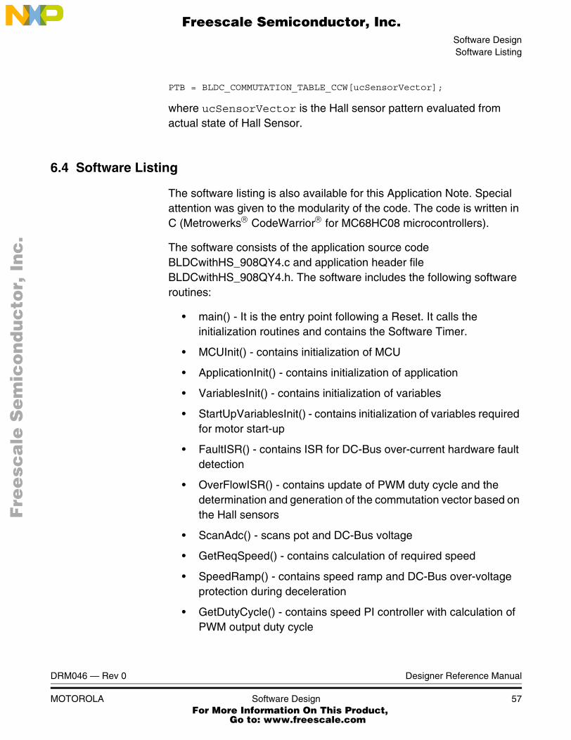
PTB = BLDC_COMMUTATION_TABLE_CCW[ucSensorVector];
where ucSensorVector is the Hall sensor pattern evaluated from actual state of Hall Sensor.
6.4 Software Listing
The software listing is also available for this Application Note. Special attention was given to the modularity of the code. The code is written in C (Metrowerks® CodeWarrior® for MC68HC08 microcontrollers).
The software consists of the application source code BLDCwithHS_908QY4.c and application header file BLDCwithHS_908QY4.h. The software includes the following software routines:
• main() - It is the entry point following a Reset. It calls the initialization routines and contains the Software Timer.
• MCUInit() - contains initialization of MCU
• ApplicationInit() - contains initialization of application
• VariablesInit() - contains initialization of variables
• StartUpVariablesInit() - contains initialization of variables required for motor start-up
• FaultISR() - contains ISR for DC-Bus over-current hardware fault detection
• OverFlowISR() - contains update of PWM duty cycle and the determination and generation of the commutation vector based on the Hall sensors
• ScanAdc() - scans pot and DC-Bus voltage
• GetReqSpeed() - contains calculation of required speed
• SpeedRamp() - contains speed ramp and DC-Bus over-voltage protection during deceleration
• GetDutyCycle() - contains speed PI controller with calculation of PWM output duty cycle
Fre
esc
ale
Se
mic
on
du
cto
r, I
Freescale Semiconductor, Inc.
For More Information On This Product, Go to: www.freescale.com
nc
...
Software Design
Designer Reference Manual DRM046 — Rev 0
58 Software Design MOTOROLA
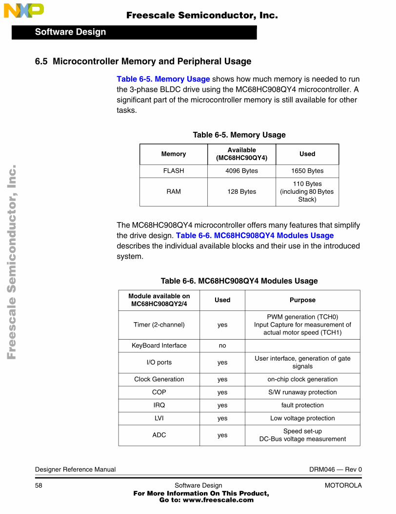
6.5 Microcontroller Memory and Peripheral Usage
Table 6-5. Memory Usage shows how much memory is needed to run the 3-phase BLDC drive using the MC68HC908QY4 microcontroller. A significant part of the microcontroller memory is still available for other tasks.
The MC68HC908QY4 microcontroller offers many features that simplify the drive design. Table 6-6. MC68HC908QY4 Modules Usage describes the individual available blocks and their use in the introduced system.
Table 6-5. Memory Usage
MemoryAvailable
(MC68HC90QY4)Used
FLASH 4096 Bytes 1650 Bytes
RAM 128 Bytes110 Bytes
(including 80 Bytes Stack)
Table 6-6. MC68HC908QY4 Modules Usage
Module available onMC68HC908QY2/4
Used Purpose
Timer (2-channel) yesPWM generation (TCH0)
Input Capture for measurement of actual motor speed (TCH1)
KeyBoard Interface no
I/O ports yesUser interface, generation of gate
signals
Clock Generation yes on-chip clock generation
COP yes S/W runaway protection
IRQ yes fault protection
LVI yes Low voltage protection
ADC yesSpeed set-up
DC-Bus voltage measurement
Fre
esc
ale
Se
mic
on
du
cto
r, I
Freescale Semiconductor, Inc.
For More Information On This Product, Go to: www.freescale.com
nc
...

DRM046 — Rev 0 Designer Reference Manual
MOTOROLA Software Design 59
POR yes Reset after Power ON
Table 6-6. MC68HC908QY4 Modules Usage
Module available onMC68HC908QY2/4
Used Purpose
Fre
esc
ale
Se
mic
on
du
cto
r, I
Freescale Semiconductor, Inc.
For More Information On This Product, Go to: www.freescale.com
nc
...

Software Design
Designer Reference Manual DRM046 — Rev 0
60 Software Design MOTOROLA
Fre
esc
ale
Se
mic
on
du
cto
r, I
Freescale Semiconductor, Inc.
For More Information On This Product, Go to: www.freescale.com
nc
...
DRM046 — Rev 0 Designer Reference Manual
MOTOROLA References 61
Designer Reference Manual — DRM046
Section 7. References
• MC68HC908QY4 Data SheetsMC68HC908QY4/D, Rev.0.1, Motorola 12/2002
• Application Note “Developer’s Serial Bootloader for M68HC08”, AN2295/D, Motorola 2003
Fre
esc
ale
Se
mic
on
du
cto
r, I
Freescale Semiconductor, Inc.
For More Information On This Product, Go to: www.freescale.com
nc
...

References
Designer Reference Manual DRM046 — Rev 0
62 References MOTOROLA
Fre
esc
ale
Se
mic
on
du
cto
r, I
Freescale Semiconductor, Inc.
For More Information On This Product, Go to: www.freescale.com
nc
...

Appendix A — Schematics and Parts ListSchematics
DRM046 — Rev 0 Designer Reference Manual
MOTOROLA Appendix A — Schematics and Parts List 63
8.1 Schematics
A set of schematics for the 3-phase BLDC drive appears in Figure 8-1. Microcontroller with Hall Sensor Input and User’s Interface, Figure 8-2. Power Stage and Figure 8-3. Power Supply. Unless otherwise specified, resistors are 1/10 watt, have a ±5% tolerance, and have values shown in ohms. Interrupted lines coded with the same letters are electrically connected.
Designer Reference Manual — DRM046
Section 8. Appendix A — Schematics and Parts List
Fre
esc
ale
Se
mic
on
du
cto
r, I
Freescale Semiconductor, Inc.
For More Information On This Product, Go to: www.freescale.com
nc
...
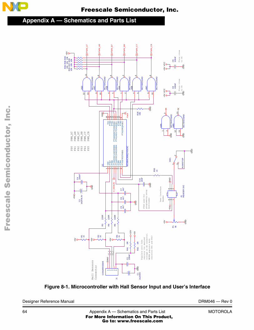
Appendix A — Schematics and Parts List
Designer Reference Manual DRM046 — Rev 0
64 Appendix A — Schematics and Parts List MOTOROLA
Figure 8-1. Microcontroller with Hall Sensor Input and User’s Interface
C8
100n
FC
910
0nF
+5V
R50
1k
VC
C
R35
10k
GN
D
+5V
VC
C
R36
10k R
3710
kR38
10k
GN
D
R39
10k
C16
10nF
GN
D
R40
10k
Place close
to U6
Place close
to U5
+5V
J3 HE
AD
ER
3X
2
246
135
+12V
GN
D
GN
D
R1
1k
+5V
R2
1k
+5V
R5
1k
+5V
+
C1
2u2/
20V
PB0 PWM_AT
PB1 PWM_AB
PB2 PWM_BT
PB3 PWM_BB
PB4 PWM_CT
PB5 PWM_CB
C2
100n
F
C4
100n
F+
C3
10uF
/6.3
V
C5
4n7
C6
4n7
C7
4n7
R3
220R
R4
220R
R6
220R
User Interface
Header
GN
D+5
V
R41
0R
+5V
R42
0R
GN
D
Populate with 0ohm
resistor for desired
voltage on HS connector.
NEVER populate both
resistors R41 and R42!
GN
D
J1
CO
N/A
RK
500/
5
1 2 3 4 5
U5C
MC
74H
C03
AD
9 108
U5B
MC
74H
C03
AD
4 56
U5D
MC
74H
C03
AD
12 1311
U5A
MC
74H
C03
AD
1 23
U6B
MC
74H
C03
AD
4 56
U6C
MC
74H
C03
AD
9 108
V_D
CB
US
PW
M_A
T
PW
M_B
T
PW
M_C
B
HS_C
HS_B
HS_A
PW
M_B
B
PW
M_C
T
PTA4 used for
programming using
bootloader
R28
10k
GN
D
Faul
t
GN
D
U6A
MC
74H
C03
AD
1 23
U6D
MC
74H
C03
AD
12 1311
GN
D
GN
D
P1 5k
+5V
GN
D
Hall Sensors
Connector
GN
D+5
VS
W1
RU
N/S
TOP
21 3
U1
MC
68H
C90
8QY
4SO
IC
Vdd
1
PTB
72
PTB
63
PTA
5/O
SC
1/A
D3/
KB
I54
PTA
4/O
SC
2/A
D2/
KB
I45
PTB
56
PTA
3/*R
ST/
KB
I38
PTB
47
PTA
2/IR
Q/K
BI2
9P
TB3
10P
TB2
11P
TA1/
AD
1/TC
H1/
KB
I112
PTA
0/A
D0/
TCH
0/K
BI0
13P
TB1
14P
TB0
15V
ss16
PW
M_A
B
Fre
esc
ale
Se
mic
on
du
cto
r, I
Freescale Semiconductor, Inc.
For More Information On This Product, Go to: www.freescale.com
nc
...

Appendix A — Schematics and Parts ListSchematics
DRM046 — Rev 0 Designer Reference Manual
MOTOROLA Appendix A — Schematics and Parts List 65
Figure 8-2. Power Stage
C21
470n
F/25
V
C26
470n
F/25
V Sou
rce_
CT
C25
100n
F
R23
470R
R20
470R
R15
470R
R16
470R
Gat
e_A
T
Gat
e_A
B
Gat
e_C
T
+12V
Faul
t
J2 Pow
er J
ack
+V
1 -V1
2
-V2 3
+12V
+12V
GN
D+12V
L1 CM
V_8
A
R14
0R01
0 - S
BL4
R13
0R01
0 - S
BL4
F1
Fuse
10A
Fas
t
D7
MU
RS
160T
3
D12
MU
RS
160T
3
Gat
e_B
T
VS0
Voltage Range
36Vdc - 56Vdc
Motor
Output
DC Power
Input
+
C24
100u
F/25
V
R11
36k
- 1%
R12
3k -
1%
U2
IR21
32S
HIN
23
LIN
26
HIN
34
LIN
37
HIN
12
LIN
15
FAU
LT8
ITR
IP9
CA
010
CA
-11
VC
C1
VS
S12
VS
126
HO
127
VB
128
LO1
16
LO2
15
LO3
14
HO
223
HO
319
VB
224
VB
320
VS
222
VS
318
VS
013
D6
MB
RS
240L
T3
V_D
CB
US
5V @ (Umax = 65V)
C17
1uF/
250V
DC
+
C18
1000
uF/6
3V
+
C19
1000
uF/6
3V
+C20
1000
uF/6
3V
D8
MB
RS
240L
T3
C35
100n
F
D13
MB
RS
240L
T3
D14
MB
RS
240L
T3
Gat
e_C
B
R17
470R
R19
470R
D11
MB
RS
240L
T3
D9
MB
RS
240L
T3
Gat
e_B
B
D18
MM
SZ5
248B
T1
J4 CO
N/A
RK
750/
2
12J5
CO
N/A
RK
750/
3
1 2 3
Sou
rce_
BT
Sou
rce_
CT
PW
M_A
T
D10
MU
RS
160T
3
PW
M_A
B
PW
M_B
TP
WM
_BB
PW
M_C
TP
WM
_CB
R44
47k
R21
82k
- 1%
D19
MM
SZ5
248B
T1R
4547
kD
20M
MS
Z524
8BT1
R22
8k2
- 1%
R46
47k
Sou
rce_
AT
VS
0
GN
D
Gat
e_A
TG
ate_
BT
Gat
e_C
T
R29
4R7
R30
4R7
D21
MM
SZ5
248B
T1R
4747
k
D5
5KP
60A
R31
4R7
R32
4R7
Q1
IRF3
710
Gat
e_A
B+48V
D23
MM
SZ5
248B
T1R
4847
k
Q2
IRF3
710
Gat
e_C
B
Q3
IRF3
710
D22
MM
SZ5
248B
T1R
4947
k
Gat
e_B
B
Q4
IRF3
710
GN
DQ
5IR
F371
0
R33
4R7
R34
4R7
Q6
IRF3
710
R43
470R
C36
22nF
GN
D
EA
RTH
_GN
D1
Heatsink Grounding
0.5V @ (Imax=10A)
Sou
rce_
AT
Sou
rce_
BT
C23
470n
F/25
V
Fre
esc
ale
Se
mic
on
du
cto
r, I
Freescale Semiconductor, Inc.
For More Information On This Product, Go to: www.freescale.com
nc
...
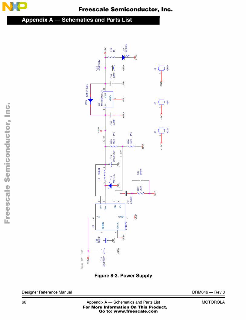
Appendix A — Schematics and Parts List
Designer Reference Manual DRM046 — Rev 0
66 Appendix A — Schematics and Parts List MOTOROLA
Figure 8-3. Power Supply
D16
MB
R16
0
+C
2747
uF/6
3V
+
C32
47uF
/6.3
V
GN
D
GN
DG
ND
U4
MC
78M
05C
DT
IN1
OU
T3
GN
D
2
D15
SM
/1N
4001
J8 GN
D
1G
ND
GN
D
+5V
Range 36V - 56V
1.24V
L233
0uH
12
J7 +5V
1
J6 +12V
1+1
2V+5
V
GN
D
+12V
U3
LT16
76
SH
DN
1
SY
NC
6
Vcc
2
Vsv
3
FB7
Vin5
GND4
Vc
8
C28
100n
F
GN
D GN
D
C33
2200
pF
R27
22
k
R25
91
k -
1%
R26
10
k -
1%
C34
100n
F
GN
D
GN
D
+48V
R24
1k
GN
D
GN
D
D17
GR
EE
N
12V DC
GN
D
C30
100n
FC
3110
0nF
+C
2910
0uF/
25V
GN
D
Fre
esc
ale
Se
mic
on
du
cto
r, I
Freescale Semiconductor, Inc.
For More Information On This Product, Go to: www.freescale.com
nc
...

Appendix A — Schematics and Parts ListParts Lists
DRM046 — Rev 0 Designer Reference Manual
MOTOROLA Appendix A — Schematics and Parts List 67
8.2 Parts Lists
The 3-phase BLDC drive’s parts content is described in Table 8-1. Parts List.
Table 8-1. Parts List
Item Designators Qty Description Manufacturer Part Number
1 C1 1 2200nF / 20Vdc tantalum size A Any acceptable
2C2,C4,C8,C9,C25,C28,C30,C31,C34, C35
9 100nF ceramic 0805 Any acceptable
3 C3 1 10µF / 6.3V tantalum size A Any acceptable
4 C5,C6,C7 3 4700pF ceramic 0805 Any acceptable
5 C16 1 10nF ceramic 0805 Any acceptable
6 C17 1metallized polyester capacitor
1.0µF / 250VDCWima MKS 4 0.1/20/250
7 C18,C19,C20 3 1000µF/63V electrolytic capacitor Panasonic ECA1JM102
8 C21,C23,C26 3 470nF/25V ceramic 1206 Any acceptable
9 C24, C29 1 100µF/25V electrolytic ELNA RVK25V101M
10 C27 1 47µF/63V electrolytic Panasonic ECA1JM470
11 C32 1 47µF / 6.3V tantalum size D Any acceptable
12 C33 1 2200pF ceramic 0805 Any acceptable
13 D5 1transient voltage suppressor
60V/5000WFagor, General
Semiconductor5KP60A
14D6,D8,D9,D11,D13,D14
6 2A 40V low Vf Schottky rectifierOn
SemiconductorMBRS240LT3
15 D7,D10,D12 3 1A 600V ultrafast rectifierOn
SemiconductorMURS160T3
16 D15 1 standard recovery diode SMDOn
Semiconductor1N4001
17 D16 1 Schottky diode 1A / 60VOn
SemiconductorMBR160
18 D17 1 green LED SMD Kingbright KP-2012MGC
19D18,D19,D20,D21,D22,D23
6 Zener diode 18V / 0.5WOn
SemiconductorMMSZ5248BT1
Fre
esc
ale
Se
mic
on
du
cto
r, I
Freescale Semiconductor, Inc.
For More Information On This Product, Go to: www.freescale.com
nc
...
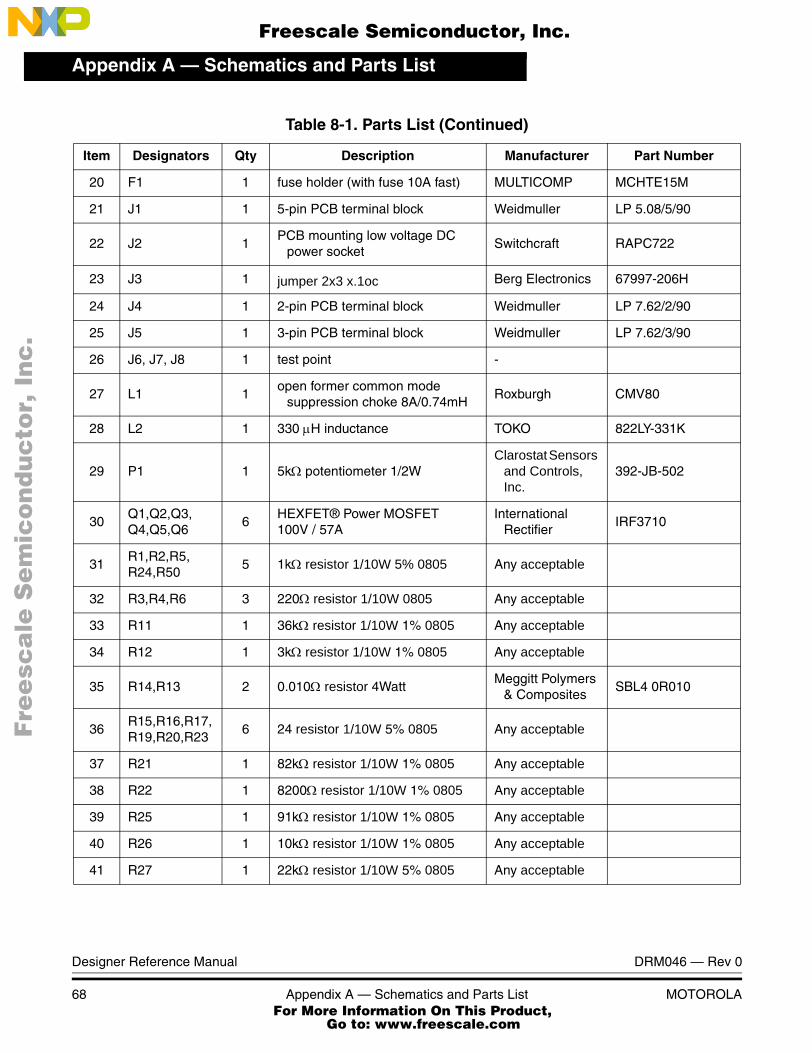
Appendix A — Schematics and Parts List
Designer Reference Manual DRM046 — Rev 0
68 Appendix A — Schematics and Parts List MOTOROLA
20 F1 1 fuse holder (with fuse 10A fast) MULTICOMP MCHTE15M
21 J1 1 5-pin PCB terminal block Weidmuller LP 5.08/5/90
22 J2 1PCB mounting low voltage DC
power socketSwitchcraft RAPC722
23 J3 1 jumper 2x3 x.1oc Berg Electronics 67997-206H
24 J4 1 2-pin PCB terminal block Weidmuller LP 7.62/2/90
25 J5 1 3-pin PCB terminal block Weidmuller LP 7.62/3/90
26 J6, J7, J8 1 test point -
27 L1 1open former common mode
suppression choke 8A/0.74mHRoxburgh CMV80
28 L2 1 330 µH inductance TOKO 822LY-331K
29 P1 1 5kΩ potentiometer 1/2WClarostat Sensors
and Controls, Inc.
392-JB-502
30Q1,Q2,Q3,Q4,Q5,Q6
6HEXFET® Power MOSFET100V / 57A
International Rectifier
IRF3710
31R1,R2,R5,R24,R50
5 1kΩ resistor 1/10W 5% 0805 Any acceptable
32 R3,R4,R6 3 220Ω resistor 1/10W 0805 Any acceptable
33 R11 1 36kΩ resistor 1/10W 1% 0805 Any acceptable
34 R12 1 3kΩ resistor 1/10W 1% 0805 Any acceptable
35 R14,R13 2 0.010Ω resistor 4WattMeggitt Polymers
& CompositesSBL4 0R010
36R15,R16,R17,R19,R20,R23
6 24 resistor 1/10W 5% 0805 Any acceptable
37 R21 1 82kΩ resistor 1/10W 1% 0805 Any acceptable
38 R22 1 8200Ω resistor 1/10W 1% 0805 Any acceptable
39 R25 1 91kΩ resistor 1/10W 1% 0805 Any acceptable
40 R26 1 10kΩ resistor 1/10W 1% 0805 Any acceptable
41 R27 1 22kΩ resistor 1/10W 5% 0805 Any acceptable
Table 8-1. Parts List (Continued)
Item Designators Qty Description Manufacturer Part Number
Fre
esc
ale
Se
mic
on
du
cto
r, I
Freescale Semiconductor, Inc.
For More Information On This Product, Go to: www.freescale.com
nc
...
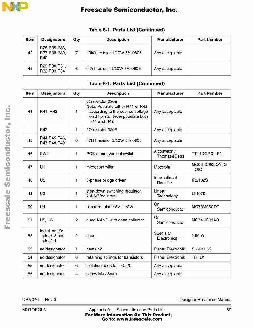
DRM046 — Rev 0 Designer Reference Manual
MOTOROLA Appendix A — Schematics and Parts List 69
42R28,R35,R36,R37,R38,R39,R40
7 10kΩ resistor 1/10W 5% 0805 Any acceptable
43R29,R30,R31,R32,R33,R34
6 4.7Ω resistor 1/10W 5% 0805 Any acceptable
Table 8-1. Parts List (Continued)
Item Designators Qty Description Manufacturer Part Number
44 R41, R42 1
0Ω resistor 0805Note: Populate either R41 or R42
according to the desired voltage on J1 pin 5. Never populate both R41 and R42
Any acceptable
R43 1 0Ω resistor 0805 Any acceptable
45R44,R45,R46,R47,R48,R49
6 47kΩ resistor 1/10W 5% 0805 Any acceptable
46 SW1 1 PCB mount vertical switchAlcoswitch /
Thomas&BettsTT11DGPC-1FN
47 U1 1 microcontroller MotorolaMC68HC908QY4S
OIC
48 U2 1 3-phase bridge driverInternational
RectifierIR2132S
49 U3 1step-down switching regulator, 7.4-60Vdc input
Linear Technology
LT1676
50 U4 1 linear regulator 5V / 1/2WOn
SemiconductorMC78M05CDT
51 U5, U6 2 quad NAND with open collectorOn
SemiconductorMC74HC03AD
52Install on J3:
pins1-3 and pins2-4
2 shuntSpecialty
Electronics2JM-G
53 no designator 1 heatsink Fisher Elektronik SK 481 85
54 no designator 6 retaining springs for transistors Fisher Elektronik THFU1
55 no designator 6 isolation pads for TO220 Any acceptable
56 no designator 4 screw M3 / 8mm Any acceptable
Table 8-1. Parts List (Continued)
Item Designators Qty Description Manufacturer Part Number
Fre
esc
ale
Se
mic
on
du
cto
r, I
Freescale Semiconductor, Inc.
For More Information On This Product, Go to: www.freescale.com
nc
...

Appendix A — Schematics and Parts List
Designer Reference Manual DRM046 — Rev 0
70 Appendix A — Schematics and Parts List MOTOROLA
57 no designator 1 pot knob Radiatron021-2220type
71-10-1/8-Black
58 no designator 5 Stick-on rubber feet Fastex 5033-01-00-5001
Table 8-1. Parts List (Continued)
Item Designators Qty Description Manufacturer Part Number
Fre
esc
ale
Se
mic
on
du
cto
r, I
Freescale Semiconductor, Inc.
For More Information On This Product, Go to: www.freescale.com
nc
...

Appendix B — System Set-upContents
DRM046 — Rev 0 Designer Reference Manual
MOTOROLA Appendix B — System Set-up 71
9.1 Contents
9.2 Hardware Setup . . . . . . . . . . . . . . . . . . . . . . . . . . . . . . . . . . . .71
9.3 Jumper Settings for Controller Board . . . . . . . . . . . . . . . . . . . .72
9.4 Required Software Tools . . . . . . . . . . . . . . . . . . . . . . . . . . . . .74
9.5 Building and Uploading the Application . . . . . . . . . . . . . . . . . .74
9.6 Executing the Application . . . . . . . . . . . . . . . . . . . . . . . . . . . . .75
9.2 Hardware Setup
Figure 9-1. Setup of the Application with BLDC Motor illustrates the hardware setup for the application. It incorporates the following modules:
• 3-phase BLDC Drive
• 3-phase BLDC motor with Hall Sensors
• Power supply 48V
Designer Reference Manual — DRM046
Section 9. Appendix B — System Set-up
Fre
esc
ale
Se
mic
on
du
cto
r, I
Freescale Semiconductor, Inc.
For More Information On This Product, Go to: www.freescale.com
nc
...

Appendix B — System Set-up
Designer Reference Manual DRM046 — Rev 0
72 Appendix B — System Set-up MOTOROLA
Figure 9-1. Setup of the Application with BLDC Motor
9.3 Jumper Settings for Controller Board
The jumper settings for the 3-phase BLDC drive board, shown in Figure 9-2. Jumper Reference of BLDC Drive Board and Table 9-1.BLDC Drive Board Jumper Settings are required to execute the 3-phase BLDC motor control application controlled by the on-board user interface.
Jumper J3 enables selection of an external user interface, as well as microcontroller flash programming using bootloader.
The zero ohms resistors R41 and R42 define the voltage level of power supply for Hall sensors available on pin 5 of Hall sensor connector J1.
• R41 populated with zero ohms resistor for +12Vdc on J5/1
Fre
esc
ale
Se
mic
on
du
cto
r, I
Freescale Semiconductor, Inc.
For More Information On This Product, Go to: www.freescale.com
nc
...
Appendix B — System Set-upJumper Settings for Controller Board
DRM046 — Rev 0 Designer Reference Manual
MOTOROLA Appendix B — System Set-up 73
• R42 populated with zero ohms resistor for +5Vdc on J5/1
WARNING: Please note that only one resistor can be accommodated according to the desired voltage; the other must be disconnected. If both resistors are populated, a short circuit might destroy the board.
Figure 9-2. Jumper Reference of BLDC Drive Board
Pot
PA4
+5V
GN
DPA
5Sw
itch
0R R42 = 0 ohms
R41 not populated J3
Table 9-1. BLDC Drive Board Jumper Settings
Jumper Comment Connections
J3 Run/Stop Switch selected Switch - PA5
J3 Speed Pot selected Pot - PA4
R42 +5Vdc selected for Hall sensor connector J1 pin 5zero ohms
resistor
Fre
esc
ale
Se
mic
on
du
cto
r, I
Freescale Semiconductor, Inc.
For More Information On This Product, Go to: www.freescale.com
nc
...
Appendix B — System Set-up
Designer Reference Manual DRM046 — Rev 0
74 Appendix B — System Set-up MOTOROLA
9.4 Required Software Tools
The application requires the following software development tools:
• Metrowerks CodeWarrior for Mc68HC08 microcontrollers version 2.1 or later.
• Bootloader for 908QY4
9.5 Building and Uploading the Application
The application software is delivered as BLDCwithHS_908QY4.mcp project file with C-source and header files BLDCwithHS_908QY4.c and BLDCwithHS_908QY4.h. Using Metrowerks CodeWarrior the executable S19 file can be created. The executable file is then downloaded into MCU through the serial bootloader, or using other Motorola programming tools.
The Developer’s Serial Bootloader for M68HC08 is a low-cost, in-circuit programming solution. It allows in-circuit reprogramming of Motorola’s M68HC08 FLASH devices using standard communication media (e.g., a serial asynchronous port). Once the MCU is pre-programmed with the bootloader, the MCU memory can be modified in-circuit. Because of its ability to modify MCU memory in-circuit, the serial bootloader is an M68HC08 MCU utility that may be useful in developing applications. Please note that the bootloader can be used only for reprogramming, not for in-circuit debugging. The bootloader is described in detail in AN2295/D “Developer’s Serial Bootloader for M68HC08“.
For MCU Flash memory programming, pin PTA4 on the BLDC board should be used. The bootloader programmer is then connected to this pin - with of course, the jumper removed, disconnecting the Run/Stop switch.
R41+12Vdc not used for Hall sensor connector J1 pin 5
due to selection of +5Vdc on this pinNo connection
Table 9-1. BLDC Drive Board Jumper Settings
Jumper Comment Connections
Fre
esc
ale
Se
mic
on
du
cto
r, I
Freescale Semiconductor, Inc.
For More Information On This Product, Go to: www.freescale.com
nc
...

Appendix B — System Set-upExecuting the Application
DRM046 — Rev 0 Designer Reference Manual
MOTOROLA Appendix B — System Set-up 75
9.6 Executing the Application
The application is prepared for operation when connected to a power supply.
The drive is controlled by the RUN/STOP switch (SW1). The motor speed is set by the SPEED potentiometer (P1). If successful, the 3-phase BLDC motor will be spinning.
NOTE: If the RUN/STOP switch is set to the RUN position when the application is powered on, toggle the switch between the RUN and STOP positions to enable motor spinning. This is a protection feature preventing the motor from starting after power on.
In the case of a DC Bus over-current, DC Bus over-voltage or DC Bus under-voltage, the fault protection disables the drive. The DC Bus over-current fault state can be left by turning the RUN/STOP switch to the stop position. DC Bus over-voltage or DC Bus under-voltage fault state can be left by MCU reset.
Fre
esc
ale
Se
mic
on
du
cto
r, I
Freescale Semiconductor, Inc.
For More Information On This Product, Go to: www.freescale.com
nc
...

Appendix B — System Set-up
Designer Reference Manual DRM046 — Rev 0
76 Appendix B — System Set-up MOTOROLA
Fre
esc
ale
Se
mic
on
du
cto
r, I
Freescale Semiconductor, Inc.
For More Information On This Product, Go to: www.freescale.com
nc
...

Fre
esc
ale
Se
mic
on
du
cto
r, I
Freescale Semiconductor, Inc.
For More Information On This Product, Go to: www.freescale.com
nc
...

HOW TO REACH US:
USA/EUROPE/LOCATIONS NOT LISTED:
Motorola Literature Distribution; P.O. Box 5405, Denver, Colorado 80217 1-303-675-2140 or 1-800-441-2447
JAPAN:
Motorola Japan Ltd.; SPS, Technical Information Center, 3-20-1, Minami-Azabu Minato-ku, Tokyo 106-8573 Japan81-3-3440-3569
ASIA/PACIFIC:
Motorola Semiconductors H.K. Ltd.; Silicon Harbour Centre, 2 Dai King Street, Tai Po Industrial Estate, Tai Po, N.T., Hong Kong852-26668334
TECHNICAL INFORMATION CENTER:
1-800-521-6274
HOME PAGE:
http://motorola.com/semiconductors
Information in this document is provided solely to enable system and software
implementers to use Motorola products. There are no express or implied copyright
licenses granted hereunder to design or fabricate any integrated circuits or
integrated circuits based on the information in this document.
Motorola reserves the right to make changes without further notice to any products
herein. Motorola makes no warranty, representation or guarantee regarding the
suitability of its products for any particular purpose, nor does Motorola assume any
liability arising out of the application or use of any product or circuit, and specifically
disclaims any and all liability, including without limitation consequential or incidental
damages. “Typical” parameters which may be provided in Motorola data sheets
and/or specifications can and do vary in different applications and actual
performance may vary over time. All operating parameters, including “Typicals”
must be validated for each customer application by customer’s technical experts.
Motorola does not convey any license under its patent rights nor the rights of
others. Motorola products are not designed, intended, or authorized for use as
components in systems intended for surgical implant into the body, or other
applications intended to support or sustain life, or for any other application in which
the failure of the Motorola product could create a situation where personal injury or
death may occur. Should Buyer purchase or use Motorola products for any such
unintended or unauthorized application, Buyer shall indemnify and hold Motorola
and its officers, employees, subsidiaries, affiliates, and distributors harmless
against all claims, costs, damages, and expenses, and reasonable attorney fees
arising out of, directly or indirectly, any claim of personal injury or death associated
with such unintended or unauthorized use, even if such claim alleges that Motorola
was negligent regarding the design or manufacture of the part.
Motorola and the Stylized M Logo are registered in the U.S. Patent and Trademark Office. digital dna is a trademark of Motorola, Inc. All other product or service names are the property of their respective owners. Motorola, Inc. is an Equal Opportunity/Affirmative Action Employer.
© Motorola, Inc. 2003
DRM046
Fre
esc
ale
Se
mic
on
du
cto
r, I
Freescale Semiconductor, Inc.
For More Information On This Product, Go to: www.freescale.com
nc
...