drv2510q1evm haptic solenoid driver evaluation · pdf filedrv2510q1evm haptic solenoid driver...
TRANSCRIPT

1SLOU449–June 2016Submit Documentation Feedback
Copyright © 2016, Texas Instruments Incorporated
DRV2510Q1EVM Haptic Solenoid Driver Evaluation Kit
User's GuideSLOU449–June 2016
DRV2510Q1EVM Haptic Solenoid Driver Evaluation Kit
ABSTRACTThe DRV2510Q1 is an automotive qualified, haptic solenoid driver that can provide up to 3 A of outputcurrent drive. The driver features simplifies the design of solenoid control for haptic effects and reducesthe total solution size. This evaluation kit provides an easy way to test any solenoid with pre-loaded orcustomizable waveforms to achieve different haptic effects. The EVM board includes the following:• MSP430 MCU• On-board EEPROM• Selectable external analog inputs or pre-loaded/customizable PWM waveforms• EMC Filter• Small footprint (70 mm × 75 mm)
Evaluation Kit Contents:• DRV2510Q1EVM evaluation board• Firmware preloaded onto on-board EEPROM• Downloadable Haptics Control Console to control EVM• Micro USB cable
The following is required for programming and advanced configuration:• Code Composer Studio™ (CCS) or IAR Embedded Workbench IDE for MSP430• MSP430 LaunchPad (MSP-EXP430G2), or MSP430-FET430UIF hardware programming tool• DRV2510Q1EVM firmware available on DRV2510Q1EVM tool folder
1 WARNING: EXPORT NOTICERecipient agrees to not knowingly export or re-export, directly or indirectly, any product or technical data(as defined by the U.S., EU, and other Export Administration Regulations) including software, or anycontrolled product restricted by other applicable national regulations, received from Disclosing party underthis Agreement, or any direct product of such technology, to any destination to which such export or re-export is restricted or prohibited by U.S. or other applicable laws, without obtaining prior authorization fromU.S. Department of Commerce and other competent Government authorities to the extent required bythose laws. This provision shall survive termination or expiration of this Agreement. According to our bestknowledge of the state and end-use of this product or technology, and in compliance with the exportcontrol regulations of dual-use goods in force in the origin and exporting countries, this technology isclassified as follows:
US ECCN: 3E991
EU ECCN: EAR99
Technology may also require export or re-export license for shipping it in compliance with the applicableregulations of certain countries.

WARNING: EXPORT NOTICE www.ti.com
2 SLOU449–June 2016Submit Documentation Feedback
Copyright © 2016, Texas Instruments Incorporated
DRV2510Q1EVM Haptic Solenoid Driver Evaluation Kit
Figure 1. DRV2510Q1EVM Board

USB
MSP430 DRV2510
12V
IN+
IN-
OUT+
OUT+
SCL
SDA
www.ti.com Getting Started
3SLOU449–June 2016Submit Documentation Feedback
Copyright © 2016, Texas Instruments Incorporated
DRV2510Q1EVM Haptic Solenoid Driver Evaluation Kit
Cautions and Warning
Warning! Do not leave EVM powered when unattended.
Warning Hot Surface! Contace may cause burns. Do not touch. Please take the proper precautions whenoperating.
2 Getting StartedThe DRV2510Q1EVM provides an evaluation of platform for different solenoids and driving waveforms. Itcan also be used as a demonstration board allowing access to both the MSP430 and DRV2510Q1through multiple test points. Input type can be controlled using Haptics Control Console for theDRV2510Q1EVM. The input is generated by an MSP430F5510 by using PWM signals. The EVM also hasthe option for the DRV2510Q1 to receive inputs externally through the jumpers available on the board ifnecessary. Figure 2 below is the block diagram:
Figure 2. EVM System Block Diagram

Getting Started www.ti.com
4 SLOU449–June 2016Submit Documentation Feedback
Copyright © 2016, Texas Instruments Incorporated
DRV2510Q1EVM Haptic Solenoid Driver Evaluation Kit
2.1 Powering the BoardTo power the board, connect the DRV2510Q1EVM to an available USB port on your computer using theincluded Micro-USB cable. When USB power is applied, the TL760M33Q will take the 5-V supply voltagedown to a regulated 3.3 V. The green 3.3-V LED will turn on and the MSP430 will be powered on. Topower the DRV2510Q1, external power must be supplied through header J5. The driver will power onwhen the external power supply provides at least 4.5 V.
2.2 Quick Start Board SetupThe DRV2510Q1EVM comes preprogrammed to use with Haptics Control Console. Figure 3 below is ascreenshot of Haptics Control Console:
Figure 3. Haptics Control Console
1. Out of the box, the on-board MSP430 is set to receive commands from Haptics Control Consolethrough the USB.
2. Use the included Micro-USB cable to connect the DRV2510Q1EVM board to an available USB port ona computer. The green 3.3-V LED will turn on and the MSP430 will be powered.
3. Once the latest version of Haptics Control Console has opened, and the device is connected to yourcomputer, you will see that the USB tab will read out '0.TI DRV2510Q1 EVM v1.[version]'. WhenHaptics Control Console has recognized the DRV2510Q1EVM, press 'Connect' to access the deviceConsole window.

3.3 kΩ 3.3 kΩ
3.3 kΩ0.015 µF0.015 µF
J9
IN+
J10
GND
GND GND GND
PWM+
3
2
1
DRV2510Q1FROM
MSP430 1 2
3.3 kΩ 3.3 kΩ
3.3 kΩ0.015 µF0.015 µF
J6
IN-
J8
GND
GND GND GND
PWM-
3
2
1
FROM
MSP430 1 2
IN+
IN-
www.ti.com Getting Started
5SLOU449–June 2016Submit Documentation Feedback
Copyright © 2016, Texas Instruments Incorporated
DRV2510Q1EVM Haptic Solenoid Driver Evaluation Kit
2.3 Configuring the InputOut of the box, the jumpers are set to connect a USB cable for microcontroller power, and drive theDRV2510Q1 inputs from an MSP430 through a 2nd order low pass filter. Table 1 shows the summary ofthe possible configurations for the input signal:
Table 1. Input Jumper Configurations
Jumper Default Position DescriptionJ9 Open (+) bypass 2nd order filter (When Shorted)J6 Open (–) bypass 2nd order filter (When Shorted)J10 Short Pin 1-2 (+) PWM from MSP430J8 Short Pin 1-2 (–) PWM from MSP430
Figure 4. Input 2nd Order Filter
As seen above in Figure 4, J9 & J6 provide the user the option to filter the input signal (IN+ or IN-) comingfrom either the MSP430 or external source. If an external input is used, remove the jumper that isconnected to the MSP430 (Pin 1 on J10 & J8) to avoid potential damage to the MCU.
When using an external input, the 2nd order filter is utilized by connecting the input signal to Pin 2 of J10& J8 (assuming J9 and J6 are open). To bypass the 2nd order filter, connect the external input signaldirectly to Pin 2 of J9 & J6, or connect the external input signal to Pin 2 of J10 & J8, and short jumpers J9and J6.
2.4 Connecting a LoadTo begin, caution is advised as the DRV2510Q1 is a high-current device that can provide up to 3 A ofoutput current drive. Also, solenoids can become hot after extended use. Be conscious of the current andtemperature ratings of the solenoid, as application of pulses and waveforms for an extended period cancause damage to the solenoids.1. With the power supply off, connect either +/– terminals on header J7 of the DRV2510Q1EVM to the
solenoid. Polarity only matters if the user is using a polarized solenoid.2. Once the connection is made and no interrupts have been triggered, inputs can be applied. Refer to

Overview of EVM www.ti.com
6 SLOU449–June 2016Submit Documentation Feedback
Copyright © 2016, Texas Instruments Incorporated
DRV2510Q1EVM Haptic Solenoid Driver Evaluation Kit
the solenoids datasheet to operate within the recommended specifications.
3 Overview of EVMThis section provides a description of each of the blocks identified in the diagram from Figure 2.
3.1 DRV2510Q1The DRV2510Q1 is an automotive qualified high-current haptic driver, specifically designed for inductiveloads. Please see the DRV2510Q1 datasheet for more in depth information.
3.2 MSP430F5510An onboard MSP430F5510 is used to control input signals to the DRV2510Q1 and the as well ascommunicate through USB to Haptics Control Console. See the Section 3.4 section for more informationabout the interface .
3.3 TL760M33QThis automotive-grade, fixed-output LDO converts the incoming 5 V from USB down to 3.3 V for theMSP430.
3.4 Haptics Control ConsoleHaptics Control Console allows the user to control the DRV2510Q1, using the on-board MSP430. TheDRV2510Q1 has I2C communication on board allowing the user to control the gain, enable pin, standbypin, and have fault and status notifications for troubleshooting and debugging.
As seen in Figure 5 below, the console contains a set of controls to manipulate the PWM Input Frequency,PWM Voltage Percentage, and duration of the PWM signal.

www.ti.com Overview of EVM
7SLOU449–June 2016Submit Documentation Feedback
Copyright © 2016, Texas Instruments Incorporated
DRV2510Q1EVM Haptic Solenoid Driver Evaluation Kit
Figure 5. DRV2510Q1EVM Haptics Control Console
3.4.1 PWM Input FrequencyIn the Standard Drive tab, the PWM input frequency can be changed using either a slider bar or bymanually entering a frequency value. The minimum frequency is 1 Hz and the maximum frequency can beup to 65 kHz. The optimum frequency for solenoid operation is less than 200 Hz.
3.4.2 PWM Voltage PercentagePWM Voltage Percentage selects the max input range to the DRV2510Q1. The full scale output voltage ofthe MSP430 is in the range of 3.3 V.
3.4.3 PWM Signal ControlLocated below the input Enable/Disable on the bottom right of Figure 5, the user has the ability to selectduration of the PWM input signal coming from the MSP430. The PWM signal can be driven continuously,in pulses (with control of on and off time), or with a single pulse (with control of the pulse duration). Thecontrol mode can be changed by clicking on the "continuous" button that will dynamically change to thetype of signal control selected.
3.4.4 SettingsIn the settings section, the user can control the gain, internal oscillator frequency, enable pin and Hi-Z pin.To operate the device be sure to have the enable pin high and Hi-Z pin low.

Hardware Configuration www.ti.com
8 SLOU449–June 2016Submit Documentation Feedback
Copyright © 2016, Texas Instruments Incorporated
DRV2510Q1EVM Haptic Solenoid Driver Evaluation Kit
The DRV2510Q1 contains integrated on-board diagnostics, which notifies the user of Over-Temperature,DC-Offset, PVDD Overvoltage/Undervoltage, Overcurrent, and 40-V Load Dump protection per ISO7637-2. These fault conditions can be seen on the Haptics Control Console, along with another set of status bitsproviding user friendly control when evaluating the DRV2510Q1.
4 Hardware ConfigurationThe DRV2510Q1EVM can be used to completely evaluate the DRV2510Q1. The following sections list thevarious hardware configurations.
4.1 Input, Output, & Communication OverviewThe DRV2510Q1EVM allows complete evaluation of the DRV2510Q1 through test points, jacks, andconnectors. Table 2 provides a brief description of the hardware.
Table 2. Hardware Overview
Signal Description I/OVIN External Supply Power (5 V - 18 V) InputUSB USB power (5 V) Input
IN+/IN- J10 (Pin2) Positive differential input; J9 bypass 2nd order filter (When shorted)J8 (Pin2) Negative differential input; J6 bypass 2nd order filter (When shorted) Input
OUT+/OUT– J7 Output to Inductive Load Output
OUTA/OUTB Output test points for observation, connect to oscilloscope or measurementequipment Output
FSR Force Sensing Resistor Input InputI2C/SCL/SDA MSP430 I2C bus/DRV2510Q1 I2C Bus Input/Output
SBW MSP430 programming header Input/OutputINT Output test point for INTZ of the DRV2510Q1 OutputTDO JTAG data output OutputTCLK System input clock InputTMS Signal to control the JTAG state machine InputTCK JTAG clock input Input
FAULT General fault reporting: Over-temp, Over-current, Under-voltage, over-voltageFault = High, normal operation; Fault = Low, Fault Condition LED
DRVON DRV Enable = LED On; DRV Disable = LED Off LED
INPUT ON MSP430 PWM input enabled = LED OnMSP430 PWM input disabled = LED Off LED
3.3 V MSP430 Powered On/Off LED
4.2 Power Supply OverviewThe DRV2510Q1EVM relies on USB and an external power supply to operate completely. Refer toTable 3 for the power supply configurations.
Table 3. Power Supply Configuration
Parameter Source Supply Voltage RangeMSP430 Micro-USB 5.0 V (LDO drops it down to 3.3 V)DRV2511Q1 J5 Terminal Block 5.0 V to 18 V
4.3 PWM, Analog and Single-Ended InputsBy default, the DRV2510Q1EVM uses the MSP430 PWM input mode with a 2nd order low-pass filter. Thissection describes each input mode and the modifications necessary for operation of each.
The DRV2510Q1EVM-HV500 supports two input modes for driving the DRV2510Q1:

100 k100 k470 pF 470 pF
OUT
OUT- OUT+
www.ti.com Hardware Configuration
9SLOU449–June 2016Submit Documentation Feedback
Copyright © 2016, Texas Instruments Incorporated
DRV2510Q1EVM Haptic Solenoid Driver Evaluation Kit
• PWM input using MSP430: In this mode, the onboard MSP430 generates a PWM waveform that issent through the 2nd order low-pass input filter to the DRV2510Q1.
• External analog input: An external source supplies an analog waveform to the INPUT header. The low-pass input filter can be bypassed as described in Section 2.3.– Single Ended Inputs: Connect the external analog input to either Pin 2 of J8 or J10. Refer to
Section 2.3 for more detailed input configuration.– Differential Input: Connect the external analog inputs across J8 and J10 using Pin 2 on each
jumper. Refer to Section 2.3 for more detailed input configuration.
4.4 Gain Setting and Master / SlaveThe gain of the DRV2511Q1 is set by the voltage divider connected to the GAIN control pin. An internalADC is used to detect the four input states. The four states set the DRV2511Q1 with gains of 20 dB, 26dB, 32 dB, 36 dB respectively. The gain setting is latched during power-up and cannot be changed whilethe device is powered. Table 4 shows the recommended resistor values for each mode and gaincombination:
(1) Resistor tolerance should be 5% or better.(2) R40 resistor is 0603(3) R41 resistor is 0805
Table 4. Gain Settings
GAIN R40 (to VREG) (1) (2) R41 (to GND) (1) (3) INPUT IMPEDANCE20 dB OPEN 20 kΩ 60 kΩ26 dB 100 kΩ 20 kΩ 30 kΩ32 dB 100 kΩ 39 kΩ 15 kΩ36 dB 75 kΩ 47 kΩ 9 kΩ
5 Measurement and AnalysisThe DRV2511Q1 uses PWM modulation to create the output signal for both solenoids and voice coils. Tomeasure the output signals, connect an oscilloscope or other measurement equipment to the filteredoutput test points, “OUT+” and “OUT-”.
Figure 6. Terminal Block and Test Points
The DRV2511Q1 PWM modulation frequency is set by default at 400 kHz. Solenoids and voice coils donot operate at this high of frequencies and will only be affected by the modulated output waveform. Formeasurement purposes, the output waveform needs to pass through a low-pass filter with a cutofffrequency around 3.38 kHz. If the DRV2511Q1EVM filter is not used, TI recommends using a first-order,low-pass filter with a cutoff between 1 kHz and 3.5 kHz.
6 ReferenceThis section includes the DRV2511Q1EVM schematic, PCB Layout and bill of materials

VDD
STDBY
EN
VDD
PWM+
FROM MSP430
EN
J9
IN+
3.3k
R4
3.3k
R5
3.3kR6
GND
FROM MSP430 PWM+
GND
0.1µFC20
10µFC21
GNDGND
GND
GND
3.3R17
DNP
DNP 3.3R18
DNP
DNP
GND GND
1
2
3
J10
2200pFC19
0.082µFC18
GNDGND
VIN = 4.5-18VDC
1µFC10
DNPDNP
SCLSDA
PWM-
J6
IN-
3.3k
R8
3.3k
R9
0.015µFC26
3.3kR11
GND
FROM MSP430 PWM-
GND
GND
1
2
3
J8
TP12
OUTA
100kR2
470pFC15
GND
100kR3
470pFC22
GND
TP13
OUTB
0.015µFC27
0.015µFC36
0.015µFC37
330µFC24
DNP
GND
470pFC33
DNPDNP 470pF
C34
DNPDNP
SCLSDA
TP14
GND
GND
TP15
GND
GND
TP4
GND
GND
TP5
GND
GND
STDBY
TP3INT
GND1
EN2
REG3
SDA4
SCL5
IN+6
IN-7
STDBY8
GND9
BSTN10
OUT-11
OUT+12
BSTP13
INTZ14
VDD15
GND16
PAD17
U1
DRV2510QPWPRQ1
0.22µFC25
0.22µFC32
GND
OUT+
OUT-
1µFC23
GND
INT
DNP
22µFC14
GND
4.7µFC17
GND
4.7µFC16
GNDGND
GND
OUT+OUT-
IN+IN-
IN+
IN-
INTTO LED
J7
OUT
J5
VIN
D24.7µFC6
GND
1
2
3
J3
I2C
GND
P6.0/CB0/A01
P6.1/CB1/A12
P6.2/CB2/A23
P6.3/CB3/A34
P5.0/A8/VEREF+5
P5.1/A9/VEREF-6
AVCC17
P5.4/XIN8
P5.5/XOUT9
AVSS110
DVCC111
DVSS112
VCORE13
P1.0/TA0CLK/ACLK14
P1.1/TA0.015
P1.2/TA0.116
P1.3/TA0.217
P1.4/TA0.318
P1.5/TA0.419
P1.6/TA1CLK/CBOUT20
P1.7/TA1.021
P2.0/TA1.122
PJ.0/TDO23
PJ.1/TDI/TCLK24
PJ.2/TMS25
PJ.3/TCK26
DVSS227
DVCC228
P4.0/PM_UCB1STE/PM_UCA1CLK29
P4.1/PM_UCB1SIMO/PM_UCB1SDA30
P4.2/PM_UCB1SOMI/PM_UCB1SCL31
P4.3/PM_UCB1CLK/PM_UCA1STE32
P4.4/PM_UCA1TXD/PM_UCA1SIMO33
P4.5/PM_UCA1RXD/PM_UCA1SOMI34
P4.6/PM_NONE35
P4.7/PM_NONE36
VSSU37
PU.0/DP38
PUR39
PU.1/DM40
VBUS41
VUSB42
V1843
AVSS244
P5.2/XT2IN45
P5.3/XT2OUT46
TEST/SBWTCK47
RST/NMI/SBWTDIO48
QFN PAD49
U4
MSP430F5510IRGZR
GND
27.0
R24
D-
D+
PWM+PWM-
0.1µFC13
0.1µFC12
0.22µFC9
0.22µFC7
0.47µFC8
GND
3.3V
47pFC4
47pFC5
GND
GND
0.1µFC11
3.3kR26
3.3kR27
1.00kR33
5V-USB
D+
D-
GND
GND
GND GND GND
GND GND
5V-USB
GreenD4
DRV ON
499
R37
A01
SDA5
A23
A12
WP7
VSS4
SCL6
VCC8
PAD9
U3
SCLSDA
J1
FSR
220pFC3
1.00k
R12 ADC2
3
1A
V+
V-
84
U2ALM358AD
0
R140
R10DNPDNP
GND GND
3.3V
3.3V 3.3V
SDASCL
EN-MSP
100kR16
GND
GND
1.00kR15
GND
INT
INT
3.3V
SDASCL
STDBY
STDBY
FSR
3.3V
GreenD5
INPUT ON
499
R39
DRV-ON
INPUT-ON
GND
5V-USB
2 1
S2
BSL
100R32
1.40kR30
1.0MR31
GND
TP6TDO
TP7TCLK
TP8TMS
TP9TCK
1.00kR34
1.00kR35
GND
TO DUTEN
IO11
IO22
GND3
IO34
IO45
VCC6
U5
TPD4E004DRYR
D+D-
0
R13
PWM+ TOPWM-
INPUT FILTER
GreenD3
3.3V
499R38
3.3V
GND
18pFC38
GND
18pFC39
1
2
3
4
5
6
J4
SBW
SBWTCKSBWTDIO
GND
9.76kR36
3.3V
SBWTDIOSBWTCK
DRV-ON
TDOTCLKTMSTCK
ADC
DPDMPUR
INPUT-ON
FROM DUT
TP1P1.0
TP2P1.1
0.1µFC29
GND
3.3V
0.1µFC30
GND
5V-USB
VDD
S3
SEL
GND
ADC
GND
IN1
OUT3
4
U6TL760M33QKVURQ1
3.3V
10µFC1
GND
5V-USB0.1µFC35
GND
0R19
DNPDNP
0R23
GND
10µFC2
GND
0.1µFC31
GND
VUSB
VUSB
27.0
R29
0R28
1.00k
R40DNPDNP
GND
1
3
2
S1Shutdown
1.2kR21
EN
GND
9.76k
R253.3V
P1.1
9.76kR1
3.3V
100kR20
3.3V
P1.0
Red
D1
FAULT499
R22
3.3V
INT
FROM DUT
I2CSCL
SDA
TP10
SCL
TP11
SDA
VBUS1
D-2
D+3
ID4
GND5
67
89
J2USB-IN
1
3 4
2GG
24MHz
Y1
Reference www.ti.com
10 SLOU449–June 2016Submit Documentation Feedback
Copyright © 2016, Texas Instruments Incorporated
DRV2510Q1EVM Haptic Solenoid Driver Evaluation Kit
6.1 Schematics
Figure 7. DRV2510Q1 Schematic 1
Figure 8. DRV2510Q1 Schematic 2

FID2
DNP
FID1
DNP
FID3
DNP
AAP068
A
PCB Number:
PCB Rev:
Assembly NoteZZ1
These assemblies are ESD sensitive, ESD precautions shall be observed.
Assembly NoteZZ2
These assemblies must be clean and free from flux and all contaminants. Use of no clean flux is not acceptable.
Assembly NoteZZ3
These assemblies must comply with workmanship standards IPC-A-610 Class 2, unless otherwise specified.
H1
SJ61A1
H2
SJ61A1
H3
SJ61A1
H4
SJ61A1
5
6
7B
V+
V-
84
U2BLM358AD
1.00k
R7
GND
GND
3.3V
GND
GND
3.3V
10.0kR41
0.1µFC28
SHUNTS
SH2 SH3SH1
www.ti.com Reference
11SLOU449–June 2016Submit Documentation Feedback
Copyright © 2016, Texas Instruments Incorporated
DRV2510Q1EVM Haptic Solenoid Driver Evaluation Kit
Figure 9. DRV2510Q1 Schematic 3

Reference www.ti.com
12 SLOU449–June 2016Submit Documentation Feedback
Copyright © 2016, Texas Instruments Incorporated
DRV2510Q1EVM Haptic Solenoid Driver Evaluation Kit
6.2 PCB Layout
Figure 10. All Layers

www.ti.com Reference
13SLOU449–June 2016Submit Documentation Feedback
Copyright © 2016, Texas Instruments Incorporated
DRV2510Q1EVM Haptic Solenoid Driver Evaluation Kit
Figure 11. Top Layer

Reference www.ti.com
14 SLOU449–June 2016Submit Documentation Feedback
Copyright © 2016, Texas Instruments Incorporated
DRV2510Q1EVM Haptic Solenoid Driver Evaluation Kit
Figure 12. Signal Layer 1

www.ti.com Reference
15SLOU449–June 2016Submit Documentation Feedback
Copyright © 2016, Texas Instruments Incorporated
DRV2510Q1EVM Haptic Solenoid Driver Evaluation Kit
Figure 13. Signal Layer 2

Reference www.ti.com
16 SLOU449–June 2016Submit Documentation Feedback
Copyright © 2016, Texas Instruments Incorporated
DRV2510Q1EVM Haptic Solenoid Driver Evaluation Kit
Figure 14. Bottom Layer

www.ti.com Reference
17SLOU449–June 2016Submit Documentation Feedback
Copyright © 2016, Texas Instruments Incorporated
DRV2510Q1EVM Haptic Solenoid Driver Evaluation Kit
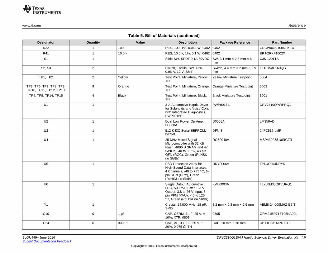
6.3 Bill Of Materials
Table 5. Bill of Materials
Designator Quantity Value Description Package Reference Part Number!PCB1 1 Printed Circuit Board AAP068C1, C2 2 10 µf CAP, CERM, 10 µF, 16 V, ±
20%, X5R, 08050805 0805YD106MAT2A
C3 1 220 pF CAP, CERM, 220 pF, 50 V, ±10%, X7R, 0402
0402 C1005X7R1H221K
C4, C5 2 47 pF CAP, CERM, 47 pF, 50 V, ±5%, C0G/NP0, 0402
0402 GRM1555C1H470JA01D
C6 1 4.7 µf CAP, CERM, 4.7 µF, 25 V, ±10%, X7R, 1206
1206 GRM31CR71E475KA88L
C7, C9 2 0.22 µf CAP, CERM, 0.22 µF, 6.3 V,± 10%, X6S, 0402
0402 GRM155C80J224KE01D
C8 1 0.47 µf CAP, CERM, 0.47 µF, 10 V, ±10%, X7R, 0603
0603 C0603C474K8RACTU
C11, C12, C13, C28, C29,C30, C31, C35
8 0.1 µf CAP, CERM, 0.1 µF, 16 V, ±10%, X7R, 0402
0402 GRM155R71C104KA88D
C14 1 22 µf CAP, CERM, 22 µF, 35 V, ±20%, X5R, 0805
0805 C2012X5R1V226M125AC
C15, C22 2 470 pF CAP, CERM, 470 pF, 50 V, ±10%, X7R, 0402
0402 GRM155R71H471KA01D
C16, C17 2 4.7 µf CAP, CERM, 4.7 µF, 50 V, ±10%, X7R, 1206_190
1206_190 UMK316AB7475KL-T
C18 1 0.082 µf CAP, CERM, 0.082 µF, 50 V,± 10%, X7R, 0603
0603 GRM188R71H823KA93D
C19 1 2200 pF CAP, CERM, 2200 pF, 50 V,± 10%, X7R, 0603
0603 GRM188R71H222KA01D
C20 1 0.1 µf CAP, CERM, 0.1 µF, 50 V, ±10%, X7R, 0603
0603 GRM188R71H104KA93D
C21 1 10 µf CAP, CERM, 10 µF, 25 V, ±10%, X7R, 1206
1206 GRM31CR71E106KA12L
C23 1 1 µf CAP, CERM, 1 µF, 16 V, ±10%, X7R, 0603
0603 C1608X7R1C105K080AC
C25, C32 2 0.22 µf CAP, CERM, 0.22 µF, 50 V, ±10%, X7R, 0603
0603 C1608X7R1H224K080AB
C26, C27, C36, C37 4 0.015 µf CAP, CERM, 0.015 µF, 16 V,± 10%, X7R, 0603
0603 GRM188R71C153KA01D
C38, C39 2 18 pF CAP, CERM, 18 pF, 50 V, ±5%, C0G/NP0, 0402
0402 GRM1555C1H180JA01D

Reference www.ti.com
18 SLOU449–June 2016Submit Documentation Feedback
Copyright © 2016, Texas Instruments Incorporated
DRV2510Q1EVM Haptic Solenoid Driver Evaluation Kit
Table 5. Bill of Materials (continued)Designator Quantity Value Description Package Reference Part Number
D1 1 Red LED, Red, SMD Red LED, 1.6 mm × 0.8 mm ×0.8 mm
LTST-C190CKT
D2 1 5.6 V Diode, Zener, 5.6 V, 500 mW,SOD-123
SOD-123 MMSZ5232B-7-F
D3, D4, D5 3 Green LED, Green, SMD LED_0805 LTST-C171GKTH1, H2, H3, H4 4 Bumpon, Cylindrical, 0.312 ×
0.200, BlackBlack Bumpon SJ61A1
J1, J6, J9 3 Header, 100 mil, 2 × 1, Tin,TH
Header, 2 PIN, 100 mil, Tin PEC02SAAN
J2 1 Connector, Receptacle,Micro-USB Type AB, R/A,Bottom Mount SMT
Connector, USB Micro AB DX4R205JJAR1800
J3, J8, J10 3 Header, 100 mil, 3 × 1, Tin,TH
Header, 3 × 1, 100 mil, TH 5-146278-3
J4 1 Receptacle, 50 mil, 6 × 1,Gold, R/A, TH
6 × 1 Receptacle LPPB061NGCN-RC
J5, J7 2 Terminal Block, 2 × 1, 3.81mm, 24-16 AWG, 10 A, 300VAC, TH
2 × 1 Terminal Block 691214310002
R1, R25, R36 3 9.76 k RES, 9.76 k, 1%, 0.063 W,0402
0402 CRCW04029K76FKED
R2, R3, R20 3 100 k RES, 100 k, 0.1%, 0.063 W,0603
0603 CPF0603B100KE
R4, R5, R6, R8, R9, R11,R26, R27
8 3.3 k RES, 3.3 k, 5%, 0.063 W,0402
0402 CRCW04023K30JNED
R7, R12, R15, R33, R34, R35 6 1.00 k RES, 1.00 k, 1%, 0.063 W,0402
0402 CRCW04021K00FKED
R13, R14, R28 3 0 RES, 0, 5%, 0.1 W, 0603 0603 RC0603JR-070RLR16 1 100 k RES, 100 k, 5%, 0.063 W,
04020402 CRCW0402100KJNED
R21 1 1.2 k RES, 1.2 k, 5%, 0.063 W,0402
0402 CRCW04021K20JNED
R22, R37, R38, R39 4 499 RES, 499 Ω, 1%, 0.1W, 0603 0603 CRCW0603499RFKEAR23 1 0 RES, 0, 5%, 0.125 W, 0805 0805 CRCW08050000Z0EA
R24, R29 2 27 RES, 27.0, 1%, 0.1 W, 0603 0603 RC0603FR-0727RLR30 1 1.40 k RES, 1.40 k, 1%, 0.063 W,
04020402 CRCW04021K40FKED
R31 1 1.0 Meg RES, 1.0 M, 5%, 0.063 W,0402
0402 CRCW04021M00JNED
www.ti.com Reference
19SLOU449–June 2016Submit Documentation Feedback
Copyright © 2016, Texas Instruments Incorporated
DRV2510Q1EVM Haptic Solenoid Driver Evaluation Kit
Table 5. Bill of Materials (continued)Designator Quantity Value Description Package Reference Part Number
R32 1 100 RES, 100, 1%, 0.063 W, 0402 0402 CRCW0402100RFKEDR41 1 10.0 k RES, 10.0 k, 1%, 0.1 W, 0402 0402 ERJ-2RKF1002XS1 1 Slide SW, SPDT 0.1A 50VDC SW, 3.1 mm × 2.5 mm × 6
mmCJS-1201TA
S2, S3 2 Switch, Tactile, SPST-NO,0.05 A, 12 V, SMT
Switch, 4.4 mm × 2 mm × 2.9mm
TL1015AF160QG
TP1, TP2 2 Yellow Test Point, Miniature, Yellow,TH
Yellow Miniature Testpoint 5004
TP3, TP6, TP7, TP8, TP9,TP10, TP11, TP12, TP13
9 Orange Test Point, Miniature, Orange,TH
Orange Miniature Testpoint 5003
TP4, TP5, TP14, TP15 4 Black Test Point, Miniature, Black,TH
Black Miniature Testpoint 5001
U1 1 3-A Automotive Haptic Driverfor Solenoids and Voice Coilswith Integrated Diagnostics,PWP0016B
PWP0016B DRV2510QPWPRQ1
U2 1 Dual Low Power Op Amp,D0008A
D0008A LM358AD
U3 1 512 K I2C Serial EEPROM,DFN-8
DFN-8 24FC512-I/MF
U4 1 25 MHz Mixed SignalMicrocontroller with 32 KBFlash, 4096 B SRAM and 47GPIOs, -40 to 85 °C, 48-pinQFN (RGC), Green (RoHS&no Sb/Br)
RGZ0048A MSP430F5510IRGZR
U5 1 ESD-Protection Array forHigh-Speed Data Interfaces,4 Channels, -40 to +85 °C, 6-pin SON (DRY), Green(RoHS& no Sb/Br)
DRY0006A TPD4E004DRYR
U6 1 Single Output AutomotiveLDO, 500 mA, Fixed 3.3 VOutput, 3.8 to 26 V Input, 3-pin PFM (KVU), -40 to 125°C, Green (RoHS& no Sb/Br)
KVU0003A TL760M33QKVURQ1
Y1 1 Crystal, 24.000 MHz, 18 pF,SMD
3.2 mm × 0.8 mm × 2.5 mm ABM8-24.000MHZ-B2-T
C10 0 1 µf CAP, CERM, 1 µF, 25 V, ±10%, X7R, 0805
0805 GRM21BR71E105KA99L
C24 0 330 µf CAP, AL, 330 µF, 25 V, ±20%, 0.075 Ω, TH
CAP, 10 mm × 16 mm UBT1E331MPD1TD

Reference www.ti.com
20 SLOU449–June 2016Submit Documentation Feedback
Copyright © 2016, Texas Instruments Incorporated
DRV2510Q1EVM Haptic Solenoid Driver Evaluation Kit
Table 5. Bill of Materials (continued)Designator Quantity Value Description Package Reference Part NumberC33, C34 0 470 pF CAP, CERM, 470 pF, 50 V, ±
5%, C0G/NP0, 06030603 06035A471JAT2A
FID1, FID2, FID3 0 Fiducial mark. There isnothing to buy or mount.
Fiducial N/A
R10 0 0 RES, 0, 5%, 0.1 W, 0603 0603 RC0603JR-070RLR17, R18 0 3.3 RES, 3.3, 5%, 0.1 W, 0603 0603 CRCW06033R30JNEA
R19 0 0 RES, 0, 5%, 0.75 W, 2010 2010 CRCW20100000Z0EFR40 0 1.00 k RES, 1.00 k, 1%, 0.063 W,
04020402 CRCW04021K00FKED

IMPORTANT NOTICE
Texas Instruments Incorporated and its subsidiaries (TI) reserve the right to make corrections, enhancements, improvements and otherchanges to its semiconductor products and services per JESD46, latest issue, and to discontinue any product or service per JESD48, latestissue. Buyers should obtain the latest relevant information before placing orders and should verify that such information is current andcomplete. All semiconductor products (also referred to herein as “components”) are sold subject to TI’s terms and conditions of salesupplied at the time of order acknowledgment.TI warrants performance of its components to the specifications applicable at the time of sale, in accordance with the warranty in TI’s termsand conditions of sale of semiconductor products. Testing and other quality control techniques are used to the extent TI deems necessaryto support this warranty. Except where mandated by applicable law, testing of all parameters of each component is not necessarilyperformed.TI assumes no liability for applications assistance or the design of Buyers’ products. Buyers are responsible for their products andapplications using TI components. To minimize the risks associated with Buyers’ products and applications, Buyers should provideadequate design and operating safeguards.TI does not warrant or represent that any license, either express or implied, is granted under any patent right, copyright, mask work right, orother intellectual property right relating to any combination, machine, or process in which TI components or services are used. Informationpublished by TI regarding third-party products or services does not constitute a license to use such products or services or a warranty orendorsement thereof. Use of such information may require a license from a third party under the patents or other intellectual property of thethird party, or a license from TI under the patents or other intellectual property of TI.Reproduction of significant portions of TI information in TI data books or data sheets is permissible only if reproduction is without alterationand is accompanied by all associated warranties, conditions, limitations, and notices. TI is not responsible or liable for such altereddocumentation. Information of third parties may be subject to additional restrictions.Resale of TI components or services with statements different from or beyond the parameters stated by TI for that component or servicevoids all express and any implied warranties for the associated TI component or service and is an unfair and deceptive business practice.TI is not responsible or liable for any such statements.Buyer acknowledges and agrees that it is solely responsible for compliance with all legal, regulatory and safety-related requirementsconcerning its products, and any use of TI components in its applications, notwithstanding any applications-related information or supportthat may be provided by TI. Buyer represents and agrees that it has all the necessary expertise to create and implement safeguards whichanticipate dangerous consequences of failures, monitor failures and their consequences, lessen the likelihood of failures that might causeharm and take appropriate remedial actions. Buyer will fully indemnify TI and its representatives against any damages arising out of the useof any TI components in safety-critical applications.In some cases, TI components may be promoted specifically to facilitate safety-related applications. With such components, TI’s goal is tohelp enable customers to design and create their own end-product solutions that meet applicable functional safety standards andrequirements. Nonetheless, such components are subject to these terms.No TI components are authorized for use in FDA Class III (or similar life-critical medical equipment) unless authorized officers of the partieshave executed a special agreement specifically governing such use.Only those TI components which TI has specifically designated as military grade or “enhanced plastic” are designed and intended for use inmilitary/aerospace applications or environments. Buyer acknowledges and agrees that any military or aerospace use of TI componentswhich have not been so designated is solely at the Buyer's risk, and that Buyer is solely responsible for compliance with all legal andregulatory requirements in connection with such use.TI has specifically designated certain components as meeting ISO/TS16949 requirements, mainly for automotive use. In any case of use ofnon-designated products, TI will not be responsible for any failure to meet ISO/TS16949.
Products ApplicationsAudio www.ti.com/audio Automotive and Transportation www.ti.com/automotiveAmplifiers amplifier.ti.com Communications and Telecom www.ti.com/communicationsData Converters dataconverter.ti.com Computers and Peripherals www.ti.com/computersDLP® Products www.dlp.com Consumer Electronics www.ti.com/consumer-appsDSP dsp.ti.com Energy and Lighting www.ti.com/energyClocks and Timers www.ti.com/clocks Industrial www.ti.com/industrialInterface interface.ti.com Medical www.ti.com/medicalLogic logic.ti.com Security www.ti.com/securityPower Mgmt power.ti.com Space, Avionics and Defense www.ti.com/space-avionics-defenseMicrocontrollers microcontroller.ti.com Video and Imaging www.ti.com/videoRFID www.ti-rfid.comOMAP Applications Processors www.ti.com/omap TI E2E Community e2e.ti.comWireless Connectivity www.ti.com/wirelessconnectivity
Mailing Address: Texas Instruments, Post Office Box 655303, Dallas, Texas 75265Copyright © 2016, Texas Instruments Incorporated