drv2605l multiple erm, lra haptic driver kit · usb vbat sbw msp430 out8 out7 out6 out5 out1 out2...
TRANSCRIPT
User's GuideSLOU400–November 2014
DRV2605L Multiple ERM, LRA Haptic Driver Kit
1 IntroductionThe DRV2605L device is a haptic driver designed for linear resonant actuators (LRA) and eccentricrotating mass (ERM) motors. The device has many features that help eliminate the design complexities ofhaptic motor control including:• Reduced solution size• High-efficiency output drive• Closed-loop motor control• Quick device startup• Embedded waveform library• Auto-resonance frequency tracking
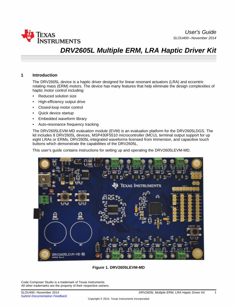
The DRV2605LEVM-MD evaluation module (EVM) is an evaluation platform for the DRV2605LDGS. Thekit includes 8 DRV2605L devices, MSP430F5510 microcontroller (MCU), terminal output support for upeight LRAs or ERMs, DRV2605L-integrated waveforms licensed from Immersion, and capacitive touchbuttons which demonstrate the capabilities of the DRV2605L.
This user’s guide contains instructions for setting up and operating the DRV2605LEVM-MD.
Figure 1. DRV2605LEVM-MD
Code Composer Studio is a trademark of Texas Instruments.All other trademarks are the property of their respective owners.
1SLOU400–November 2014 DRV2605L Multiple ERM, LRA Haptic Driver KitSubmit Documentation Feedback
Copyright © 2014, Texas Instruments Incorporated

US
B
VB
AT
SB
W
MSP430
OUT8 OUT7 OUT6 OUT5
OUT4OUT3OUT2OUT1
DRV2605L
DRV2605L DRV2605L DRV2605L DRV2605L
DRV2605L DRV2605L DRV2605L
BSL RESET
USER SW
TCA9548A
TCA9554A
B1 B2
USB Power
External Power
ProgrammerConnector
Effect Buttons
Actuator Connections
Actuator Connections
DRV2605L
DR
V
MS
P
Power selection for MSP430 and DRV2605L
Getting Started www.ti.com
2 Getting StartedThe DRV2605LEVM-MD demonstrates how the DRV2605L device can be used in applications that requiremultiple haptic drivers (same slave addresses) to be setup independently but be played simultaneously.The board integrates the TCA9548A I2C switch to control which I2C lines of the possible eight DRV2605Ldrivers are connected to the master input I2C bus. The switch has the ability to select any combination ofchannels to be connected to the master input I2C bus.
The board also integrates the MSP430F5510 device with USB interface capabilities and bootstrap loading(BSL) functionality. The USB interfacing provides the user flexibility in controlling the DRV2605L devicewithout having to modify the firmware. The BSL functionality simplifies the firmware updating processwithout the additional hardware and the use of Code Composer Studio™ software.
The board receives power in two ways. For applications that require two or less active DRV2605L devicesdevice at the same time, the board can be powered through a USB port. For applications that requiremore than two drivers, the use of the external power supply terminals with a current rating of 1.6 A isrecommended. Manual selection of USB power or external power can be set using the jumper headersMSP and DRV. When powered up, button 1 and button 2 (B1, B2) can be used to demonstrate thefunctionality of the DRV2605L device. See Section 3 for a detailed description of the demonstrationapplication program.
Figure 2. Board Diagram
2 DRV2605L Multiple ERM, LRA Haptic Driver Kit SLOU400–November 2014Submit Documentation Feedback
Copyright © 2014, Texas Instruments Incorporated

DR
VM
SP
www.ti.com Getting Started
2.1 Quick Start Board SetupThe DRV2605LEVM-MD firmware contains haptic waveform sequences that showcase the features andbenefits of the DRV2605L device in a multi-driver application. Use the following setup instructions to beginthe demand evaluation process:1. Connect 4 ERM actuators to the terminal block outputs 1 through 4, and connect 4 LRA actuators to
the terminal block outputs 5 through 8 on the board.2. Connect the 5-V power supply to the VBAT terminal block.3. Verify that the jumper connections on the board are correct as listed in Table 1.4. Turn on the power supply. If the DRV2605LEVM-MD is powered correctly, the button LEDs turn on and
flash indicating that the board has been successfully initialized.
Table 1. Default Jumper Settings for Demonstration Program
JUMPER POSITION DESCRIPTIONJ1 Shorted Connects decoupling cap to the VDD pin, used for power consumption
measurementsJ2 Shorted 3.3-V reference voltage for I2C transactions on the TCA9548A deviceJ3 Shorted User LEDJ4 Don’t care User LEDJ5 Shorted Trigger and PWM input to the DRV2605L deviceJ6 Shorted User switch
MSP Short pins 2 to 3 VBAT power to the MSP430 device (Shown in Figure 3)DRV Short pins 2 to 3 VBAT power to the DRV2605L device (Shown in Figure 3)
Figure 3. Jumper Position for MSP and DRV Headers
NOTE: This board has the ability to control both ERM and LRA actuators at the same time. Thedefault firmware is set so that only the actuators that are connected to the board are active.The connected driver and the actuator type must be hardcoded in the firmware in order forthe system to know the user’s hardware configuration. If the default configuration of 4 ERMactuators on outputs 1 through 4 and 4 LRA actuators on outputs 5 through 8 is not desired,see Section 3.4 for more details on how to customize the board.
3 DRV2605L Demonstration ProgramSeveral functionality sections can be initiated to demonstrate how the DRV2605LEVM-MD can be used formulti-driver applications. The user can interact with the capacitive touch buttons to output a variety ofwaveform sequences to the actuators externally connected to the board and to enable all the drivers andI2C channels for full access to the DRV2605L devices through the I2C headers.
The user can also access USB functionality through the user switch. The capacitive touch buttons (B1 andB2) and user switch (USER SW) have the following functionality:• B1: The DRV2605L devices are setup individually and RTP mode is configured. Sequential button
presses activate the next DRV2605L device in sequential order starting at driver 1, ending at driver 8,and then looping back to driver 1.
• B2:– Mode 1 – Enables all of the drivers and channels of the TCA9548A device for the user to gain
access to all of the DRV2605L devices.– Mode 2 – Drivers 1 through 4 are enabled, RTP mode is setup, and all drivers are played
simultaneously
3SLOU400–November 2014 DRV2605L Multiple ERM, LRA Haptic Driver KitSubmit Documentation Feedback
Copyright © 2014, Texas Instruments Incorporated

US
B
VB
AT
SB
W
MSP430
OUT8 OUT7 OUT6 OUT5
OUT4OUT3OUT2OUT1
DRV2605L
DRV2605L DRV2605L DRV2605L DRV2605L
DRV2605L DRV2605L DRV2605L
BSL RESET
USER SW
TCA9548A
TCA9554A
B1 B2
LRA
ERM
DR
V
MS
P
ERM ERM ERM
LRA LRA LRA
DRV2605L Demonstration Program www.ti.com
– Mode 3 – Drivers 5 through 8 are enabled, RTP mode is setup, and all drivers are playedsimultaneously
– Mode 4 – Driver 1 through 4 are setup in RTP mode, played sequentially in order, and then brieflyplayed simultaneously.
– Mode 5 – Driver 5 through 8 are setup in RTP mode, played sequentially in order, and then brieflyplayed simultaneously.
• USER SW: Turns on USB communication and disables capacitive touch buttons
Figure 4. Board With Actuator Setup
Figure 4 shows the actuator setup of where the LRAs and ERMs are connected to the board. B1 and B2are the capacitive touch buttons that, when pressed, play the waveform sequence as described inSection 3.1 and Section 3.2.
3.1 Button 1For button 1, each of the DRV2605L devices is independently setup for RTP mode at full magnitude 0x7Fand played sequentially. Each press of the capacitive touch button plays the next driver. The TCA9548Adevice (I2C switch) is configured so that only the corresponding DRV2605L device is connected to themaster input I2C bus. When the configuration is complete, default register settings, RTP mode, and theRTP magnitude are sent to the DRV2605L device. After some time, the RTP mode shuts off.
3.2 Button 2Button2 has 5 modes that can be accessed through sequential button presses. The user must sequentiallycycle through all of the other modes to get back into the same mode.
3.2.1 Mode 1Mode 1 allows the user full access to all of the DRV2605L devices on the board by enabling them andconnecting all of the I2C lines. An external host processor can be connected to the I2C headers to allowcommunication to the DRV2605L devices without having to use the on-board MSP430F5510.
4 DRV2605L Multiple ERM, LRA Haptic Driver Kit SLOU400–November 2014Submit Documentation Feedback
Copyright © 2014, Texas Instruments Incorporated

www.ti.com DRV2605L Demonstration Program
3.2.2 Mode 2 and Mode 3Mode 2 and mode 3 enable and connect the I2C lines for drivers 1 through 4 and drivers 5 through 8,respectively. The four DRV2605L devices are sent the same default initialization settings for the ERMactuators (Mode 2) and LRA actuators (Mode 3). The drivers are then setup in RTP mode with magnitude0x7F. The waveform plays for 2 s and then the drivers are changed to internal trigger mode (to stop RTPmode).
3.2.3 Mode 4 and Mode 5Mode 4 and mode 5 enable and connect the I2C lines for drivers 1 through 4 and drivers 5 through 8,respectively. The four DRV2605L devices are sent the same default initialization settings for ERMactuators (Mode 4) and LRA actuators (Mode 5). When the settings are received by the DRV2605Ldevices, each DRV2605L device is individually enabled sequentially and setup for RTP mode withmagnitude 0x7F at a 500-ms interval. Driver 1 or 5 outputs the RTP waveform for 500 ms, then the nextsequential drivers (driver 2 or 6, 3 or 7, 4 or 8) repeat the same conditions as driver 1. As soon as driver 4or 8 completes the waveform output, all drivers exit of RTP mode for 100 ms and then enter RTP modewith magnitude 0x7F for 100 ms to create a brief pulse action.
3.3 User SwitchAt board startup, the capacitive touch buttons are automatically enabled and USB communication isdisabled even though USB communication was initialized. To enter USB communication for use with themulti-driver graphical user interface (GUI), the user switch must be pressed. LED1 turns to indicate thatthe firmware is active for USB transactions. When the user switch is pressed and the board is in USBcommunication mode, the capacitive touch buttons are disabled. A power cycle or software reset isrequired to go back to capacitive-touch mode.
3.4 Firmware ModificationsBefore the board can accept any combination of LRA and ERM actuators connected to the DRV2605Ldevices, the firmware is required to be modified because it must know which actuators are connected towhich haptic drivers. Additional hardware-like dip switches are required to detect real-time changes withactuators or enable the drivers. The header file, haptics.h, contains the definitions of driver 1 throughdriver 8, and actuator 1 through actuator 8 which are mapped to arrays that are used in haptic methods asfollows:• Haptics_DriversEnableConfig()• Haptics_EnableAvailableDrivers()• Haptics_ActuatorTypeConnected()• Haptics_SwitchAvailableDrivers()
The driver definitions can be either CONNECTED or NOT_CONNECTED. The actuator definitions can beeither ACTUATOR_ERM or ACTUATOR_LRA. When each definition is defined properly, the methodsprovided configure the TCA9554A and TCA9548A devices to enable the DRV2605L devices and connectthe I2C lines of the drivers to the master I2C bus properly.
5SLOU400–November 2014 DRV2605L Multiple ERM, LRA Haptic Driver KitSubmit Documentation Feedback
Copyright © 2014, Texas Instruments Incorporated

OUT 470 pF
OUT+ OUT±
100 k 100 k
470 pF
From DRV2605L
Measurement and Analysis—Waveform Sequences www.ti.com
4 Measurement and Analysis—Waveform SequencesThe DRV2605L device uses PWM modulation to create the output signal for both ERM and LRAactuators. To measure and observe the DRV2605L output waveform, connect an oscilloscope or othermeasurement equipment to the filtered output test points, OUT+ and OUT–. Figure 5 shows the setup ofthe terminal block and test points used to connect external actuators and measure waveforms.
Figure 5. Terminal Block and Test Points
4.1 TripleClick and StrongClick Example WaveformsFigure 6 displays the tripleClick waveform output for an LRA (trace C1 and C2) and the strongClickwaveform for an ERM (trace C3 and C4) the same time. The differential output (trace Math) is trace C1-CT the ERM was operated in open-loop mode while the LRA was operated in auto-resonance (closedloop) mode.
Figure 6. TripleClick and StrongClick Waveform Played at the Same Time
6 DRV2605L Multiple ERM, LRA Haptic Driver Kit SLOU400–November 2014Submit Documentation Feedback
Copyright © 2014, Texas Instruments Incorporated

www.ti.com Measurement and Analysis—Waveform Sequences
4.2 Pulsing Strong Example WaveformsFigure 7 displays the pulsingStrong waveform output for an ERM (trace C1, C2). The differential output(trace Math) is trace C1-CT the ERM was operated in open-loop mode. The peak acceleration for thewaveform is 156.1 mVPP or 1.37 G.
Figure 7. Pulsing Strong waveform for ERM in Open-Loop Mode
7SLOU400–November 2014 DRV2605L Multiple ERM, LRA Haptic Driver KitSubmit Documentation Feedback
Copyright © 2014, Texas Instruments Incorporated

Measurement and Analysis—Waveform Sequences www.ti.com
4.3 Strong Buzz Example WaveformsFigure 8 and Figure 9 show the output waveform (trace C1 and C2), the differential output (trace Math),and the acceleration profile (trace C4) for the buzz waveform. Figure 8 displays the waveform in auto-resonance mode while Figure 9 displays the same waveform in open-loop mode. Auto-resonance modeallows the acceleration profile to have a higher peak acceleration at a lower VRMS voltage.
Figure 8. Strong Buzz Waveform for LRA in Auto-Resonance Mode
Figure 9. Strong Buzz Waveform for LRA in Open-Loop Mode
8 DRV2605L Multiple ERM, LRA Haptic Driver Kit SLOU400–November 2014Submit Documentation Feedback
Copyright © 2014, Texas Instruments Incorporated
www.ti.com TCA9554 - I2C GPIO Expander
5 TCA9554 - I2C GPIO ExpanderThe TCA9554 GPIO expander is used to enable the DRV2605L device. Because the multi-driver boardhas the ability to control up to 8 haptic drivers, the TCA9554 device is able to control the enable lines ofthe DRV2605L device through I2C and free up GPIO pin space on the MSP430F5510 device for otherperipherals. The following pseudo code shows how the TCA9554 device is used as an outputconfiguration.I2C_SetSlaveAddr(TCA9554_SLAVE_ADDR) //setslave addressI2C_WriteSingleByte(0x03, ~(bit_set_for_output)) //configure as output portI2C_WriteSingleByte(0x01, output_bits) //output values
The TCA9554 device is configured completely through I2C commands. The expander must be configuredas an output port for the corresponding drivers (8 drivers). The output port command register is 0x03.Each bit of the 8-bit value represents the 8 output ports of the device. A value of zero in each bitcorresponds to an output configuration. The variable, bit_set_for_output, has the respective bits set asoutputs. When the output port is configured, register 0x03 does not need to be accessed unless thoseports will be used as some other port function. After the ports are configured as outputs, a write commandto register 0x01 is used to set the value of the output to either 0 or 1. The default values for outputs areinitialized to 0. See the TCA9554 data sheet, SCPS233, for more information on the TCA9554 device.
5.1 I2C Register Value ExamplesThe following examples listed in Table 2 and Table 3 show exact I2C transactions with slave addresses,registers, and values to enable one DRV2605L device and to enable three or more DRV2605L devices.
Table 2. TCA9554 I2C Transaction for Enabling driver 1Slave Address (7-bit) Register Value DescriptionI2C Action
Configures IO expander for output port at1 Write 0x20 0x03 0xFE channel 1
2 Write 0x20 0x01 0x01 Sends a high signal to output channel 1
Table 3. TCA9554 I2C Transaction for Enabling drivers 1, 4, 5, and 8Slave Address (7-bit) Register Value DescriptionI2C Action
Configures IO expander for output port at1 Write 0x20 0x03 0x66 channel 1, 4, 5, and (corresponds to drivers
1, 4, 5, 8).
Sends a high signal to output channel 1, 4,2 Write 0x20 0x01 0x99 5, and (corresponds to drivers 1, 4, 5, 8).
6 TCA9548A - I2C SwitchThe DRV2605LEVM-MD is designed for multi-driver applications. The TCA9548A I2C switch was used toindependently setup haptic drivers and play the waveforms simultaneously. The pseudo code listed in thefollowing code allows the user to verify proper operation of the I2C switch and communication with theDRV2605L device.I2C_SetSlaveAddr(TCA9548_SLAVE_ADDR) //setslave addressI2C_WriteSingleByte(driver_position) //channelselection
This code lists the sequence for how to command the TCA9548A I2C switch. Any combination of channelscan be selected. When the slave address of the TCA9548A device is set, a single byte is required toinitialize channel selection. No register address is needed to send the channel selection value, but if aregister input must be available for the I2C write function, use the data value as the register value becausethe device will take the last byte sent to it.
9SLOU400–November 2014 DRV2605L Multiple ERM, LRA Haptic Driver KitSubmit Documentation Feedback
Copyright © 2014, Texas Instruments Incorporated

TCA9548A - I2C Switch www.ti.com
6.1 I2C Register Value ExamplesThe examples listed in Table 4 and Table 5 show exact I2C transactions with slave addresses, registers,and values to enable one DRV2605L device and to enable three or more DRV2605L devices.
Table 4. TCA9548A I2C Transaction for Enabling Driver 1
I2C Action Slave Address (7-bit) Register Value DescriptionConfigures I2C switch to connect1 Write 0x70 N/A 0x01 channel 1 I2C lines
Table 5. TCA9548A I2C Transaction for Enabling Driver 1, 4, 5, and 8
I2C Action Slave Address (7-bit) Register Value DescriptionConfigures I2C switch to contact
1 Write 0x70 N/A 0x99 channel 1, 4, 5, and (corresponds todrivers 1, 4, 5, 8).
6.2 Operation AnalysisThe TCA9548A operation can be verified with a logic analyzer hooked up to the master I2C bus input intothe device and to the channel outputs. Figure 10 shows the data and clock lines of the I2C commands tothe switch and to the GPIO expander to show proper operation of the devices together.
Figure 10. TCA9548A Logic Analyzer Operation
The TCA9554 device is first configured for output ports for drivers 6 and 7 with a value of 1 at the output.The TCA9548A device is switched to driver 7 (channel 8) and sent a read command to the DRV2605Ldevice to verify communication with the haptic driver. The switch is then configured to select driver 6(channel 7) and is then sent the same read command. Figure 10 shows proper operation of the switch inthe case of isolating specific channels.
10 DRV2605L Multiple ERM, LRA Haptic Driver Kit SLOU400–November 2014Submit Documentation Feedback
Copyright © 2014, Texas Instruments Incorporated
US
B
VB
AT
BSL RESET
DR
VM
SP
USB
VBAT
www.ti.com Power Supply Selection
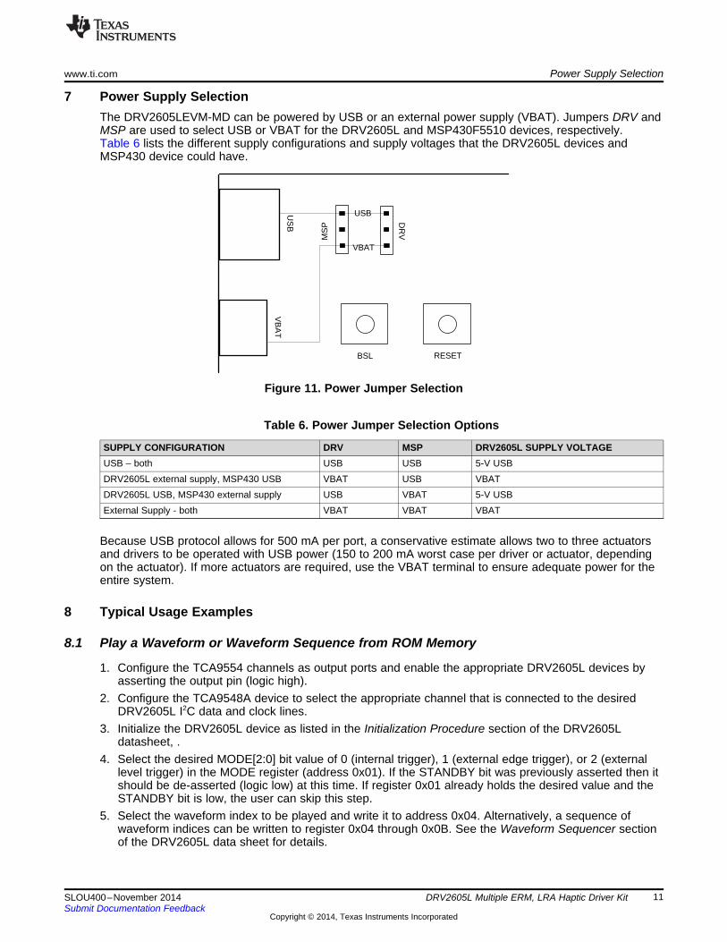
7 Power Supply SelectionThe DRV2605LEVM-MD can be powered by USB or an external power supply (VBAT). Jumpers DRV andMSP are used to select USB or VBAT for the DRV2605L and MSP430F5510 devices, respectively.Table 6 lists the different supply configurations and supply voltages that the DRV2605L devices andMSP430 device could have.
Figure 11. Power Jumper Selection
Table 6. Power Jumper Selection Options
SUPPLY CONFIGURATION DRV MSP DRV2605L SUPPLY VOLTAGEUSB – both USB USB 5-V USBDRV2605L external supply, MSP430 USB VBAT USB VBATDRV2605L USB, MSP430 external supply USB VBAT 5-V USBExternal Supply - both VBAT VBAT VBAT
Because USB protocol allows for 500 mA per port, a conservative estimate allows two to three actuatorsand drivers to be operated with USB power (150 to 200 mA worst case per driver or actuator, dependingon the actuator). If more actuators are required, use the VBAT terminal to ensure adequate power for theentire system.
8 Typical Usage Examples
8.1 Play a Waveform or Waveform Sequence from ROM Memory
1. Configure the TCA9554 channels as output ports and enable the appropriate DRV2605L devices byasserting the output pin (logic high).
2. Configure the TCA9548A device to select the appropriate channel that is connected to the desiredDRV2605L I2C data and clock lines.
3. Initialize the DRV2605L device as listed in the Initialization Procedure section of the DRV2605Ldatasheet, .
4. Select the desired MODE[2:0] bit value of 0 (internal trigger), 1 (external edge trigger), or 2 (externallevel trigger) in the MODE register (address 0x01). If the STANDBY bit was previously asserted then itshould be de-asserted (logic low) at this time. If register 0x01 already holds the desired value and theSTANDBY bit is low, the user can skip this step.
5. Select the waveform index to be played and write it to address 0x04. Alternatively, a sequence ofwaveform indices can be written to register 0x04 through 0x0B. See the Waveform Sequencer sectionof the DRV2605L data sheet for details.
11SLOU400–November 2014 DRV2605L Multiple ERM, LRA Haptic Driver KitSubmit Documentation Feedback
Copyright © 2014, Texas Instruments Incorporated

Typical Usage Examples www.ti.com
6. If using the internal trigger mode, set the Go bit (in register 0x0C) to fire the effect or sequence ofeffects. If using an external trigger mode, send an appropriate trigger pulse to the IN/TRIG pin. See theWaveform Triggers section of the DRV2605L datasheet for details.
7. If desired, the user can repeat step 5 to figure the effect or sequence again.8. Put the device in low-power mode by deasserting the EN pin through the TCA9554 device to set the
STANDBY bit.
NOTE: To send the same commands to multiple DRV2605L devices at the same time, configure theTCA9554 and TCA9548A devices to the appropriate channel selections. I2C write functionscan be sent to multiple DRV2605L device, but I2C read functions for each DRV2605L devicemust be read individually. One issue with write functions is the inability to properly determinewhether multiple DRV2605L devices are ACK (acknowledge) or NACK (not acknowledge) ifthe same command was sent, however writing actual bytes to the DRV2605L is not aproblem. The bus acts as an AND bus and logic zero takes priority.
Table 7 lists examples of the I2C transactions that are required to play a triple click (100%) waveformusing driver 1 in LRA, closed-loop mode. The yellow highlighted rows indicate auto-calibration mode andobtaining the results for the auto-calibration compensation and back-EMF results (if required to beperformed for the first time).
Table 7. I2C Transaction Example of Playing a Triple Click Waveform Using Driver1 in LRA, ClosedLoop mode
SLAVEDEVICE ADDRESS REGISTER VALUE DESCRIPTIONI2C ACTION
(7-BIT)
1 Write TCA9554 0x20 0x03 0xFE Configures IO expander for output port at channel 1
2 Write TCA9554 0x20 0x01 0x01 Sends a high signal to output channel 1
3 Write TCA9548A 0x70 N/A 0x01 Configures I2C switch to connect channel 1 I2C lines
4 Write DRV2605L 0x5A 0x16 0x53 Set rated voltage (2 VRMS)
5 Write DRV2605L 0x5A 0x17 0xA4 Set overdrive clamp voltage (3.6-V peak)
6 Write DRV2605L 0x5A 0x01 0x07 Change mode to AutoCalibration
7 Write DRV2605L 0x5A 0x1E 0x20 Set AutoCalTime to 500 ms
8 Write DRV2605L 0x5A 0x0C 0x01 Set GO Bit
9 Read DRV2605L 0x5A 0x0C Poll GO Bit until it clears to 0
12 Write DRV2605L 0x5A 0x1A 0xB6 Set feedback control register
13 Write DRV2605L 0x5A 0x1B 0x93 Set control 1 register
14 Write DRV2605L 0x5A 0x1C 0xF5 Set control 2 register
15 Write DRV2605L 0x5A 0x1D 0x80 Set control 3 register
16 Write DRV2605L 0x5A 0x01 0x00 Set mode to internal trigger
17 Write DRV2605L 0x5A 0x04 0x0C Set waveform sequence 1 as triple-click waveform
18 Write DRV2605L 0x5A 0x05 0x00 Indicator that there is only one waveform thatshould be played
19 Write DRV2605L 0x5A 0x0C 0x01 Set GO bit
20 Read DRV2605L 0x5A 0x0C Poll GO bit until it clears to 0
21 Write TCA9554 0x20 0x00 0x00 Deassert the EN pin for driver 1
22 Write TCA9548A 0x70 N/A 0x00 No driver I2C channels connected
12 DRV2605L Multiple ERM, LRA Haptic Driver Kit SLOU400–November 2014Submit Documentation Feedback
Copyright © 2014, Texas Instruments Incorporated

www.ti.com Programming the MSP430
9 Programming the MSP430
9.1 Bootstrap Loader MethodThe following items are required to program the board using the bootstrap loading (BSL) method:• Mini USB cable• MSP430 USB firmware upgrade which is found in the MSP430 USB developers package
(www.ti.com/tool/msp430usbdevpack)• Code Composer Studios (CCS)
Use the following steps to program the board using the BSL method:1. Open the firmware project in CCS and go to the build menu of the properties window as shown in
Figure 12.2. Under the Steps tab of the build menu and in the Apply Predefined Step drop-down, select Create
flash image: TI-TXT as shown in Figure 12.
Figure 12. CCS Create Flash Image
3. Rebuild the project. The text image file can be found in debug folder with the name AIP032.txt4. Hold the BSL button on the DRV2605LEVM-MD and connect the EVM to the computer through the
USB mini cable to initiate it as a USB device.5. Open up the MSP430 USB Firmware Uploader. If it does not say ready on the screen then retry the
BSL powerup sequence again.6. Go to file and select open user firmware to locate the text image file (Figure 13 shows an example
of a successful firmware update process).7. Cycle the power on the board to restart the firmware.
13SLOU400–November 2014 DRV2605L Multiple ERM, LRA Haptic Driver KitSubmit Documentation Feedback
Copyright © 2014, Texas Instruments Incorporated

Programming the MSP430 www.ti.com
Figure 13. MSP430 USB Firmware Uploader Programming Sequence
9.2 Spy-By-Wire MethodThe following items are required to program the board using the spy-by-wire (SBW) method.• Mini USB cable• MSP-JTAG2SBW Adapter• MSP-FET430UIF Hardware Debugging Interface• Code Composer Studios (CCS)
Use the following steps to program the board using the SBW method:1. Connect the MSP-JTAG2SBW adapter to the SBW connector on the board2. Connect the MSP-FET430UIF to the MSP-JTAG2SBW adapter.3. Open up the firmware project in CCS.4. Verify that the general-build properties are set as shown in Figure 14.5. Right click on the project title folder under the project explorer and click build project to ensure that no
errors exist.6. If no errors exist, select RUN → DEBUG in the title bar.7. Exit the debugger when the firmware has been uploaded to the board.
Figure 14. Build Properties of Firmware Project
14 DRV2605L Multiple ERM, LRA Haptic Driver Kit SLOU400–November 2014Submit Documentation Feedback
Copyright © 2014, Texas Instruments Incorporated

www.ti.com Programming the MSP430
9.3 MSP430 PinoutTable 8 lists the pin functions the MSP430F5510 device. The yellow highlighted rows indicate pins that areused by the board. The non-highlighted rows indicate unused pins. All GPIO pins that are not highlightedare broken out to standard 100-mil pitch headers for prototype development and evaluation.
Table 8. Used and Unused Pins on the MSP430F5510PIN
DESCRIPTIONNO. NAME
1 P6.0/CB0/A0 Button 1
2 P6.1/CB1/A1 Button 2
3 P6.2/CB2/A2
4 P6.3/CB3/A3
5 P6.4/CB4/A4
6 P6.5/CB5/A5
7 P6.6/CB6/A6
8 P6.7/CB7/A7
9 P5.0/A8
10 P5.1/A9
11 AVCC1 3.3 V
12 P5.4/XIN XIN, 32.768-kHz crystal
13 P5.5/XOUT XOUT, 32.768-kHz crystal
14 AVSS1 GND
15 DVCC1 3.3 V
16 DVSS1 GND
17 VCORE Decoupling capacitor for VCore
18 P1.0/TA0CLK
19 P1.1/TA0.0
20 P1.2/TA0.1
21 P1.3/TA0.2
22 P1.4/TA0.3
23 P1.5/TA0.4
24 P1.6/TA1CLK/CBOUT COMP_OUT, Feedback from B1 and B2 captouch
25 P1.7/TA1.0
26 P2.0/TA1.1
27 P2.1/TA1.2
28 P2.2/TA2CLK/SMCLK
29 P2.3/TA2.0
30 P2.4/TA2.1 PWM, can be disconnected
31 P2.5/TA2.2
32 P2.6/RTCCLK/DMAE0
33 P2.7/UCB0STE/UCA0CLK
34 P3.0/UCB0SIMO/UCB0SDA
35 P3.1/UCB0SOMI/UCB0SCL
36 P3.2/UCB0CLK/UCA0STE
37 P3.3/UCA0TXD/UCA0SIMO
38 P3.4/UCA0RXD/UCA0SOMI
39 DVSS2 GND
40 DVCC2 3.3 V
41 P4.0/PM_UCB1STE/PM_UCA1CLK
42 P4.1/PM_UCB1SIMO/PM_UCB1SDA SDA_IN
43 P4.2/PM_UCB1SOMI/PM_UCB1SCL SCL_IN
44 P4.3/PM_UCB1CLK/PM_UCA1STE
45 P4.4/PM_UCA1TXD/PM_UCA1SIMO
46 P4.5/PM_UCA1RXD/PM_UCA1SOMI
15SLOU400–November 2014 DRV2605L Multiple ERM, LRA Haptic Driver KitSubmit Documentation Feedback
Copyright © 2014, Texas Instruments Incorporated

Programming the MSP430 www.ti.com
Table 8. Used and Unused Pins on the MSP430F5510 (continued)PIN
DESCRIPTIONNO. NAME
47 P4.6/PM_NONE
48 P4.7/PM_NONE
49 VSSU GND
50 PU.0/DP USB_DP, data+
51 PUR PUR, BSL switch
56 AVSS2 GND
57 P5.2/XT2IN XT2IN, 24-MHz oscillator
58 P5.3/XT2OUT XT2OUT, 24-MHz oscillator
59 TEST/SBWTCK SBWTCK, SBW programmer conn.
60 PJ.0/TDO B1LED
61 PJ.1/TDI/TCLK B2LED
62 PJ.2/TMS USER LED1, can be disconnected
63 PJ.3/TCK USER LED2, can be disconnected
64 nRST/NMI/SBWTDIO ResistorET button, SBW programmer
65 QFN PAD GND
16 DRV2605L Multiple ERM, LRA Haptic Driver Kit SLOU400–November 2014Submit Documentation Feedback
Copyright © 2014, Texas Instruments Incorporated

www.ti.com Layout
10 Layout
Figure 15. Xray Image of Top and Bottom Layer Traces
Figure 16. Top Layer
Figure 17. Middle Power Layer
17SLOU400–November 2014 DRV2605L Multiple ERM, LRA Haptic Driver KitSubmit Documentation Feedback
Copyright © 2014, Texas Instruments Incorporated
Layout www.ti.com
Figure 18. Middle Ground Layer
Figure 19. Bottom Layer
18 DRV2605L Multiple ERM, LRA Haptic Driver Kit SLOU400–November 2014Submit Documentation Feedback
Copyright © 2014, Texas Instruments Incorporated

MSP430F5510
I2C SwitchTCA9548A
I2C IO ExpanderTCA9554
I2C- Data
I2C-Clock
Haptic DriverDRV2605L
Haptic DriverDRV2605L
Haptic DriverDRV2605L
Haptic DriverDRV2605L
Haptic DriverDRV2605L
Haptic DriverDRV2605L
Haptic DriverDRV2605L
Haptic DriverDRV2605L
8
8
I2C Bus Lines
2
2
2
22
2
2
2
I2C
Bus
Lin
es
8
Power Input
USB or External VCC
Power Muxing
TPS22910A
TPS22912C
+3.3V LDO
TPS73633+5V +3.3V
Power Management
Capacitive Touch Buttons
www.ti.com Schematic
11 Schematic
Figure 20. Schematic Block Diagram
19SLOU400–November 2014 DRV2605L Multiple ERM, LRA Haptic Driver KitSubmit Documentation Feedback
Copyright © 2014, Texas Instruments Incorporated

1µFC5
0.1µFC3
GND
GND 1
2
OUT1
100k
R1
470pFC1
100k
R3
470pFC7
GND
GND
OUT1+
OUT1-Green
ENABLE1
1.5kR5
GND
OUT1+
OUT1-
SDA1
GND
PWMREG
1
SCL2
SDA3
IN/TRIG4
EN5
VDD/NC6
OUT+7
GND8
OUT-9
VDD10
U1
DRV2605LDGS
SCL1
1µFC6
0.1µFC4
GND
GND 1
2
OUT2
100k
R2
470pFC2
100k
R4
470pFC8
GND
GND
OUT2+
OUT2-Green
ENABLE2
1.5kR6
GND
OUT2+
OUT2-
SDA2
GND
PWMREG
1
SCL2
SDA3
IN/TRIG4
EN5
VDD/NC6
OUT+7
GND8
OUT-9
VDD10
U2
DRV2605LDGS
SCL2
1µFC13
0.1µFC11
GND
GND 1
2
OUT3
100k
R7
470pFC9
100k
R9
470pFC15
GND
GND
OUT3+
OUT3-Green
ENABLE3
1.5kR11
GND
OUT3+
OUT3-
SDA3
GND
PWMREG
1
SCL2
SDA3
IN/TRIG4
EN5
VDD/NC6
OUT+7
GND8
OUT-9
VDD10
U3
DRV2605LDGS
SCL3
1µFC14
0.1µFC12
GND
GND 1
2
OUT4
100k
R8
470pFC10
100k
R10
470pFC16
GND
GND
OUT4+
OUT4-Green
ENABLE4
1.5kR12
GND
OUT4+
OUT4-
SDA4
GND
PWMREG
1
SCL2
SDA3
IN/TRIG4
EN5
VDD/NC6
OUT+7
GND8
OUT-9
VDD10
U4
DRV2605LDGS
SCL4
1µFC21
0.1µFC19
GND
GND
1
2
OUT5
100k
R13
470pFC17
100k
R15
470pFC23
GND
GND
OUT5+
OUT5-Green
ENABLE5
1.5kR17
GND
OUT5+
OUT5-
SDA5
GND
PWMREG
1
SCL2
SDA3
IN/TRIG4
EN5
VDD/NC6
OUT+7
GND8
OUT-9
VDD10
U5
DRV2605LDGS
SCL5
1µFC22
0.1µFC20
GND
GND
1
2
OUT6
100k
R14
470pFC18
100k
R16
470pFC24
GND
GND
OUT6+
OUT6-Green
ENABLE6
1.5kR18
GND
OUT6+
OUT6-
SDA6
GND
PWMREG
1
SCL2
SDA3
IN/TRIG4
EN5
VDD/NC6
OUT+7
GND8
OUT-9
VDD10
U6
DRV2605LDGS
SCL6
1µFC29
0.1µFC27
GND
GND
1
2
OUT7
100k
R19
470pFC25
100k
R21
470pFC31
GND
GND
OUT7+
OUT7-Green
ENABLE7
1.5kR23
GND
OUT7+
OUT7-
SDA7
GND
PWMREG
1
SCL2
SDA3
IN/TRIG4
EN5
VDD/NC6
OUT+7
GND8
OUT-9
VDD10
U7
DRV2605LDGS
SCL7
1µFC30
0.1µFC28
GND
GND
1
2
OUT8
100k
R20
470pFC26
100k
R22
470pFC32
GND
GND
OUT8+
OUT8-Green
ENABLE8
1.5kR24
GND
OUT8+
OUT8-
SDA8
GND
PWMREG
1
SCL2
SDA3
IN/TRIG4
EN5
VDD/NC6
OUT+7
GND8
OUT-9
VDD10
U8
DRV2605LDGS
SCL8
ENABLE1 ENABLE2
ENABLE3 ENABLE4
ENABLE5 ENABLE6
ENABLE7 ENABLE8
1 2
J1
VBAT
VBAT
VBAT
VBAT
VBAT
VBAT
VBAT
VBAT
Schematic www.ti.com
Figure 21. Schematic Page 1
20 DRV2605L Multiple ERM, LRA Haptic Driver Kit SLOU400–November 2014Submit Documentation Feedback
Copyright © 2014, Texas Instruments Incorporated

12
34
BSL
+3.3V
100R67
1.0MegR70
GND
0.22µFC43
0.22µFC49
0.1µFC52
GND
0.1µF
C5110µFC50
0.1µFC53
0R71
+3.3V
GND
+3.3V
GND
GND
1 2
3 4
RESET
47kR65
GND
BSL
RESET
USB_DPUSB_DM
27R66
27R69
10pFC46
10pFC47
GND
1.40kR68
0.47µF
C45
GND
4.7µF
C48
+5V_USB
GND
32.768kHz
Y212pF
C41
12pF
C42
GND
P3.2
XT2INXT2OUTXINXOUT
249
R57
249
R59
GND
P6.0/CB0/A01
P6.1/CB1/A12
P6.2/CB2/A23
P6.3/CB3/A34
P6.4/CB4/A45
P6.5/CB5/A56
P6.6/CB6/A67
P6.7/CB7/A78
P5.0/A8/VEREF+9
P5.1/A9/VEREF-10
AVCC111
P5.4/XIN12
P5.5/XOUT13
AVSS114
DVCC115
DVSS116
VCORE17
P1.0/TA0CLK/ACLK18
P1.1/TA0.019
P1.2/TA0.120
P1.3/TA0.221
P1.4/TA0.322
P1.5/TA0.423
P1.6/TA1CLK/CBOUT24
P1.7/TA1.025
P2.0/TA1.126
P2.1/TA1.227
P2.2/TA2CLK/SMCLK28
P2.3/TA2.029
P2.4/TA2.130
P2.5/TA2.231
P2.6/RTCCLK/DMAE032
P2.7/UCB0STE/UCA0CLK33
P3.0/UCB0SIMO/UCB0SDA34
P3.1/UCB0SOMI/UCB0SCL35
P3.2/UCB0CLK/UCA0STE36
P3.3/UCA0TXD/UCA0SIMO37
P3.4/UCA0RXD/UCA0SOMI38
DVSS239
DVCC240
P4.0/PM_UCB1STE/PM_UCA1CLK41
P4.1/PM_UCB1SIMO/PM_UCB1SDA42
P4.2/PM_UCB1SOMI/PM_UCB1SCL43
P4.3/PM_UCB1CLK/PM_UCA1STE44
P4.4/PM_UCA1TXD/PM_UCA1SIMO45
P4.5/PM_UCA1RXD/PM_UCA1SOMI46
P4.6/PM_NONE47
P4.7/PM_NONE48
VSSU49
PU.0/DP50
PUR51
PU.1/DM52
VBUS53
VUSB54
V1855
AVSS256
P5.2/XT2IN57
P5.3/XT2OUT58
TEST/SBWTCK59
PJ.0/TDO60
PJ.1/TDI/TCLK61
PJ.2/TMS62
PJ.3/TCK63
RST/NMI/SBWTDIO64
QFN PAD65
U13
MSP430F5510IRGC
BUTTON1BUTTON2
100k
R63
100k
R64
COMP_OUT
COMP_OUT
B1LEDB2LED
B1LED
B2LED
P1.0P1.1P1.2P1.3P1.4P1.5
P1.7
P3.3P3.4
P5.0P5.1
P2.0P2.1P2.2
P2.4P2.5P2.6P2.7
P4.3P4.4P4.5P4.6P4.7
P6.2P6.3P6.4P6.5P6.6P6.7
P2.3
Cap Touch Button LEDs
P2.0P2.1P2.2
P2.4P2.5P2.6P2.7
P2.3
GNDGNDP4.3P4.4P4.5P4.6P4.7
P6.2P6.3P6.4P6.5P6.6P6.7
COMP_OUT
P1.0P1.1P1.2P1.3P1.4P1.5
P1.7
GND
USER_LED1
USER_LED2
User LEDs
511
R58
Orange
1 2
LED2
511
R60
PJ.2PJ.3
PJ.2
PJ.3
User Switches
1 2
3 4
USER SW
47kR72
GND
+3.3V
0.68µFC54
USER_SW1 P5.0
PUR
Green
1 2
LED1
P3.2P3.3P3.4
PJ.2PJ.3
P5.0P5.1
Breakout Headers
Cool White
2 1
B1LED
Cool White
2 1
B2LED
PWM
PWM1
/RESET_SBWTDIO
+3.3VGND
VBAT VBATGND
+3.3V
+3.3VGND
+3.3V
5
4
1
2
3
6
7
8
PORT1
5
4
1
2
3
6
7
8
PORT2
5
4
1
2
3
6
7
8
PORT4
5
4
1
2
3
6
7
8
PORT6
1
2
3
PORT3_2
4
1
2
3
PORT5_J
12
J6
1 2
J31 2
J4
1 2
J5
SBWTCK
1
2
3
4
5
6
SBW
GND
Spy-By-Wire
SBWTCK/RESET_SBWTDIO
1 2
3 4
5 6
J7
47pFC44
1
34
2GG
24MHz
Y1
GND
GND
GND
0
R61
SCL_IN
0
R62
SDA_INP3.0P3.1
P4.01
2
PORT3_1P3.0P3.1
P4.0
18pF
C39
18pF
C40
www.ti.com Schematic
Figure 22. Schematic Page 2
21SLOU400–November 2014 DRV2605L Multiple ERM, LRA Haptic Driver KitSubmit Documentation Feedback
Copyright © 2014, Texas Instruments Incorporated

IN1
GND2
EN3
NR/FB4
OUT5
U11
TPS73633DBV
1
2
VBAT
282834-2
GND
1µFC33
Green
12
+3.3V
1.5kR31
GND
GND
GND
SDA_INSCL_IN
Power Management - USB/External
SDA_IN
SCL_IN
GND
SCL1SDA1
SCL2SDA2
SCL3SDA3
SCL4SDA4
SCL5SDA5
SCL6SDA6
SCL7SDA7
SCL8SDA8
A01
A12
RESET3
SD04
SC05
SD16
SC17
SD28
SC29
SD310
SC311
GND12
SD413
SC414
SD515
SC516
SD617
SC618
SD719
SC720
A221
SCL22
SDA23
VCC24
U12
TCA9548APW
+3.3V
GND
+3.3V
1µFC38
3.3kR39
3.3kR33
3.3kR32
3.3kR34
3.3kR35
3.3kR36
3.3kR37
3.3kR38
3.3kR56
3.3kR49
3.3kR50
3.3kR51
3.3kR52
3.3kR53
3.3kR54
3.3kR55
10kR40
10kR41
I2C Switch Interface
Note: Slave Addr for TCA9548A - 0x70 (7-bit)
A01
A12
A23
P04
P15
P26
P37
GND8
P49
P510
P611
P712
INT13
SCL14
SDA15
VCC16
U9
TCA9554PWR
ENABLE1ENABLE2ENABLE3ENABLE4ENABLE5ENABLE6ENABLE7ENABLE8
SCL_INSDA_IN
+3.3V
GND
Note: Slave Addr for TCA9554 - 0x20 (7-bit)
VCC1
NC2
IO13
GND4
IO25
U10
TPD2E001IDRLRQ1
2
3
4
1
5
USB
1734035-2GND
GND
VBUSUSB_DMUSB_DP
GND1
Ground Test Points for DRV2605
GND
GND2
GND
GND3
GND
GND4
GND
GND5
GND
GND6
GND
GND7
GND
GND
600 ohm
L2
600 ohm
L1
1.0kR45 1.0k
R44 1.0kR43
0R48
0R47
0R46
IO_VCC
GND
1.0kR27 1.0k
R26 1.0kR25
0R30
0R29
0R28
IO_VCC
GND
IO_VCC+3.3V
1 2
J2
1
2
3
I2C
NC
10kR42
IO_VCC
GND
1
2
3
MSP
1
2
3
DRV
+5V_USB
+5V_USB
GND
VBAT
0.1µFC35
100µF
C361µFC37
1µFC34
+5V_USB
+5V USB Test Point
+5V USB
+3.3V
Schematic www.ti.com
Figure 23. Schematic Page 3
22 DRV2605L Multiple ERM, LRA Haptic Driver Kit SLOU400–November 2014Submit Documentation Feedback
Copyright © 2014, Texas Instruments Incorporated

www.ti.com Bill Of Materials
12 Bill Of Materials
DESIGNATOR QTY. VALUE PART NUMBER DESCRIPTION PACKAGE MANUFACTURER
+3.3V, ENABLE1, ENABLE2, 10 Green LTST-C190GKT LED, green, SMD 1.6 × 0.8 × 0.8 mm Lite-OnENABLE3, ENABLE4, ENABLE5,ENABLE6, ENABLE7, ENABLE8,LED1
5 V USB 1 Red 5000 Test point, miniature, red, TH Red miniature test point Keystone
B1LED, B2LED 2 Cool White LNJ037X8ARA LED, cool white, SMD 0603 LED Panasonic
BSL, ResistorET, USER SW 3 4-1437565-1 Switch, tactile, SPST-NO, 0.05-A, 12-V, SMT SW, SPST 6 × 6 mm TE Connectivity
C1, C2, C7, C8, C9, C10, C15, 16 470 pF GRM155R71H471KA01D Capacitor, ceramic, 470-pF, 50-V, ±10%, X7R, 0402 0402 MuRataC16, C17, C18, C23, C24, C25,C26, C31, C32
C3, C4, C11, C12, C19, C20, 11 0.1 µF GRM155R61C104KA88D Capacitor, ceramic, 0.1-µF, 16-V, ±10%, X5R, 0402 0402 MuRataC27, C28, C51, C52, C53
C5, C6, C13, C14, C21, C22, 9 1 µF C1005X5R1E105K050BC Capacitor, ceramic, 1-µF, 25V, ±10%, X5R, 0402 0402 TDKC29, C30, C38
C33, C34, C37 3 1 µF GRM155R61A105KE15D Capacitor, ceramic, 1-µF, 10-V, ±10%, X5R, 0402 0402 MuRata
C35 1 0.1 µF GRM155R61A104KA01D Capacitor, ceramic, 0.1-µF, 10-V, ±10%, X5R, 0402 0402 MuRata
C36 1 100 µF C3216X5R1A107M160AC Capacitor, ceramic, 100-µF, 10-V, ±20%, X5R, 1206_190 1206_190 TDK
C39, C40 2 18 pF GRM1555C1H180JA01D Capacitor, ceramic, 18-pF, 50-V, ±5%, C0G/NP0, 0402 0402 MuRata
C41, C42 2 12 pF GRM1555C1H120JA01D Capacitor, ceramic, 12-pF, 50-V, ±5%, C0G/NP0, 0402 0402 MuRata
C43, C49 2 0.22 µF GRM155R71C224KA12D Capacitor, ceramic, 0.22-µF, 16-V, ±10%, X7R, 0402 0402 MuRata
C44 1 47 pF GRM1555C1H470JZ01 Capacitor, ceramic, 47-pF, 50-V, ±5%, C0G/NP0, 0402 0402 MuRata
C45 1 0.47 µF GRM155R61C474KE01 Capacitor, ceramic, 0.47-µF, 16-V, ±10%, X5R, 0402 0402 MuRata
C46, C47 2 10 pF GRM1555C1H100JA01D Capacitor, ceramic, 10-pF, 50-V, ±5%, C0G/NP0, 0402 0402 MuRata
C48 1 4.7 µF TPSA475K010R1400 Capacitor, TA, 4.7uF, 10-V, ±10%, 1.4 Ω, SMD 3216-18 AVX
C50 1 10 µF TPSA106K010R0900 Capacitor, TA, 10-µF, 10-V, ±10%, 0.9 Ω, SMD 3216-18 AVX
C54 1 0.68 µF GRM155R61A684KE15D Capacitor, ceramic, 0.68-µF, 10-V, ±10%, X5R, 0402 0402 MuRata
DRV, I1, MSP, PORT3_2 4 5-146278-3 Header, 100-mil, 3 × 1, tin, TH Header, 3 × 1, 100-mil, TH TE Connectivity
GND1, GND2, GND3, GND4, 7 Black 5011 Test point, multipurpose, black, TH Black multipurpose test point KeystoneGND5, GND6, GND7
H1, H2, H3, H4 4 NY PMS 440 0025 PH Machine screw, round, #4-40 × 1/4, nylon, Philips panhead Screw B&F Fastener Supply
H5, H6, H7, H8 4 1902C Standoff, hex, 0.5"L #4-40 nylon Standoff Keystone
J1, J2, J3, J4, J5, J6, PORT3_1 7 5-146278-2 Header, 100-mil, 2 × 1, Tin, TH Header, 2 × 1, 100-mil, TH TE Connectivity
J7 1 5-146254-3 Header, 100-mil, 3 × 2, Tin, TH Header, 100-mil, 3 × 2, TH TE Connectivity
L1, L2 2 600 Ω MPZ2012S601A Ferrite bead, 600-Ω at 100 MHz, 2-A, 0805 0805 TDK
LED2 1 Orange LTST-C190KFKT LED, orange, SMD 1.6 × 0.8 × 0.8 mm Lite-On
OUT1+, OUT1-, OUT2+, OUT2-, 16 White 5002 Test point, miniature, white, TH White Miniature Testpoint KeystoneOUT3+, OUT3-, OUT4+, OUT4-,OUT5+, OUT5-, OUT6+, OUT6-,OUT7+, OUT7-, OUT8+, OUT8-
OUT1, OUT2, OUT3, OUT4, 9 282834-2 Terminal block, 2 × 1, 2.54mm, TH Terminal Block, 2 × 1, 2.54- TE ConnectivityOUT5, OUT6, OUT7, OUT8, mm, THVBAT
PORT1, PORT2, PORT4, PORT6 4 5-146278-8 Header, 100-mil, 8 × 1, Tin, TH Header, 8 × 1, 100-mil, TH TE Connectivity
PORT5_J 1 5-146278-4 Header, 100-mil, 4 × 1, Tin, TH Header, 4 × 1, 100-mil, TH TE Connectivity
23SLOU400–November 2014 DRV2605L Multiple ERM, LRA Haptic Driver KitSubmit Documentation Feedback
Copyright © 2014, Texas Instruments Incorporated

Bill Of Materials www.ti.com
DESIGNATOR QTY. VALUE PART NUMBER DESCRIPTION PACKAGE MANUFACTURER
PWM1 1 Orange 5003 Test point, miniature, orange, TH Orange miniature testpoint Keystone
R1, R2, R3, R4, R7, R8, R9, R10, 18 100 kΩ CRCW0402100KJNED Resistor, 100-kΩ, 5%, 0.063 W, 0402 0402 Vishay-DaleR13, R14, R15, R16, R19, R20,R21, R22, R63, R64
R5, R6, R11, R12, R17, R18, 9 1.5 kΩ CRCW04021K50JNED Resistor, 1.5-kΩ, 5%, 0.063-W, 0402 0402 Vishay-DaleR23, R24, R31
R25, R26, R27, R43, R44, R45 0 1 kΩ CRCW04021K00JNED Resistor, 1-kΩ, 5%, 0.063-W, 0402 0402 Vishay-Dale
R28, R29, R30, R46, R47, R48, 9 0 CRCW04020000Z0ED Resistor, 0-Ω, 5%, 0.063-W, 0402 0402 Vishay-DaleR61, R62, R71
R32, R33, R34, R35, R36, R37, 16 3.3 kΩ CRCW04023K30JNED Resistor, 3.3-kΩ, 5%, 0.063-W, 0402 0402 Vishay-DaleR38, R39, R49, R50, R51, R52,R53, R54, R55, R56
R40, R41, R42 3 10 kΩ CRCW040210K0JNED Resistor, 10-kΩ, 5%, 0.063-W, 0402 0402 Vishay-Dale
R57, R59 2 249 Ω CRCW0402249RFKED Resistor, 249-Ω, 1%, 0.063-W, 0402 0402 Vishay-Dale
R58, R60 2 511 Ω CRCW0402511RFKED Resistor, 511-Ω, 1%, 0.063-W, 0402 0402 Vishay-Dale
R65, R72 2 47 kΩ CRCW040247K0JNED Resistor, 47-kΩ, 5%, 0.063-W, 0402 0402 Vishay-Dale
R66, R69 2 27 Ω CRCW040227R0JNED Resistor, 27-Ω, 5%, 0.063-W, 0402 0402 Vishay-Dale
R67 1 100 Ω CRCW0402100RJNED Resistor, 100-Ω, 5%, 0.063-W, 0402 0402 Vishay-Dale
R68 1 1.4 kΩ CRCW04021K40FKED Resistor, 1.4-kΩ, 1%, 0.063-W, 0402 0402 Vishay-Dale
R70 1 1 MΩ CRCW04021M00JNED Resistor, 1-MΩ, 5%, 0.063-W, 0402 0402 Vishay-Dale
SBW 1 LPPB061NGCN-RC Receptacle, 50-mil, 6 × 1, R/A, TH 6 × 1 receptacle Sullins Connector Solutions
U1, U2, U3, U4, U5, U6, U7, U8 8 DRV2605LDGS DRV2605LDGS, DGS0010A DGS0010A Texas Instruments
U9 1 TCA9554PWR PW0016A Texas InstrumentsRemote 8-bit I2C and SMBus I/expander, 1.65 to 5.5-V, –40 to85°C, 16-pin TSSOP (PW), green (RoHS & nSb/Br)
U10 1 TPD2E001IDRLRQ1 Automotive catalog low-capacitance ±15-kV ESD-protection DRL0005A Texas Instrumentsarray for high-speed data inter, 2 channels, –40 to 85°C, 5-pinSOT (DRL), Green (RoHS & nSb/Br)
U11 1 TPS73633DBV Capacitor-free, NMOS, 400-mA low-dropout regulator with DBV0005A Texas Instrumentsreverse current protection, DBV0005A
U12 1 TCA9548APW PW0024A Texas InstrumentsLow voltage 8-channel I2C switch with reset, PW0024A
U13 1 MSP430F5510IRGC Mixed signal microcontroller, RGC0064B RGC0064B Texas Instruments
USB 1 1734035-2 Connector, receptacle, mini-USB type B, R/A, top mount SMT USB mini type B TE Connectivity
Y1 1 ABM8-24.000MHZ-B2-T Crystal, 24-MHz, 18-pF, SMD 3.2 × 0.8 × 2.5-mm Abracon Corportation
Y2 1 MS3V-T1R 32.768KHZ ±20PPM 12.5PF Crystal, 32.768-kHz, 12.5-pF, SMD 1.4 × 1.4 × 5-mm SMD MicrCrystal AG
24 DRV2605L Multiple ERM, LRA Haptic Driver Kit SLOU400–November 2014Submit Documentation Feedback
Copyright © 2014, Texas Instruments Incorporated
STANDARD TERMS AND CONDITIONS FOR EVALUATION MODULES1. Delivery: TI delivers TI evaluation boards, kits, or modules, including any accompanying demonstration software, components, or
documentation (collectively, an “EVM” or “EVMs”) to the User (“User”) in accordance with the terms and conditions set forth herein.Acceptance of the EVM is expressly subject to the following terms and conditions.1.1 EVMs are intended solely for product or software developers for use in a research and development setting to facilitate feasibility
evaluation, experimentation, or scientific analysis of TI semiconductors products. EVMs have no direct function and are notfinished products. EVMs shall not be directly or indirectly assembled as a part or subassembly in any finished product. Forclarification, any software or software tools provided with the EVM (“Software”) shall not be subject to the terms and conditionsset forth herein but rather shall be subject to the applicable terms and conditions that accompany such Software
1.2 EVMs are not intended for consumer or household use. EVMs may not be sold, sublicensed, leased, rented, loaned, assigned,or otherwise distributed for commercial purposes by Users, in whole or in part, or used in any finished product or productionsystem.
2 Limited Warranty and Related Remedies/Disclaimers:2.1 These terms and conditions do not apply to Software. The warranty, if any, for Software is covered in the applicable Software
License Agreement.2.2 TI warrants that the TI EVM will conform to TI's published specifications for ninety (90) days after the date TI delivers such EVM
to User. Notwithstanding the foregoing, TI shall not be liable for any defects that are caused by neglect, misuse or mistreatmentby an entity other than TI, including improper installation or testing, or for any EVMs that have been altered or modified in anyway by an entity other than TI. Moreover, TI shall not be liable for any defects that result from User's design, specifications orinstructions for such EVMs. Testing and other quality control techniques are used to the extent TI deems necessary or asmandated by government requirements. TI does not test all parameters of each EVM.
2.3 If any EVM fails to conform to the warranty set forth above, TI's sole liability shall be at its option to repair or replace such EVM,or credit User's account for such EVM. TI's liability under this warranty shall be limited to EVMs that are returned during thewarranty period to the address designated by TI and that are determined by TI not to conform to such warranty. If TI elects torepair or replace such EVM, TI shall have a reasonable time to repair such EVM or provide replacements. Repaired EVMs shallbe warranted for the remainder of the original warranty period. Replaced EVMs shall be warranted for a new full ninety (90) daywarranty period.
3 Regulatory Notices:3.1 United States
3.1.1 Notice applicable to EVMs not FCC-Approved:This kit is designed to allow product developers to evaluate electronic components, circuitry, or software associated with the kitto determine whether to incorporate such items in a finished product and software developers to write software applications foruse with the end product. This kit is not a finished product and when assembled may not be resold or otherwise marketed unlessall required FCC equipment authorizations are first obtained. Operation is subject to the condition that this product not causeharmful interference to licensed radio stations and that this product accept harmful interference. Unless the assembled kit isdesigned to operate under part 15, part 18 or part 95 of this chapter, the operator of the kit must operate under the authority ofan FCC license holder or must secure an experimental authorization under part 5 of this chapter.3.1.2 For EVMs annotated as FCC – FEDERAL COMMUNICATIONS COMMISSION Part 15 Compliant:
CAUTIONThis device complies with part 15 of the FCC Rules. Operation is subject to the following two conditions: (1) This device may notcause harmful interference, and (2) this device must accept any interference received, including interference that may causeundesired operation.Changes or modifications not expressly approved by the party responsible for compliance could void the user's authority tooperate the equipment.
FCC Interference Statement for Class A EVM devicesNOTE: This equipment has been tested and found to comply with the limits for a Class A digital device, pursuant to part 15 ofthe FCC Rules. These limits are designed to provide reasonable protection against harmful interference when the equipment isoperated in a commercial environment. This equipment generates, uses, and can radiate radio frequency energy and, if notinstalled and used in accordance with the instruction manual, may cause harmful interference to radio communications.Operation of this equipment in a residential area is likely to cause harmful interference in which case the user will be required tocorrect the interference at his own expense.
SPACER
SPACER
SPACER
SPACER
SPACER
SPACER
SPACER
SPACER

FCC Interference Statement for Class B EVM devicesNOTE: This equipment has been tested and found to comply with the limits for a Class B digital device, pursuant to part 15 ofthe FCC Rules. These limits are designed to provide reasonable protection against harmful interference in a residentialinstallation. This equipment generates, uses and can radiate radio frequency energy and, if not installed and used in accordancewith the instructions, may cause harmful interference to radio communications. However, there is no guarantee that interferencewill not occur in a particular installation. If this equipment does cause harmful interference to radio or television reception, whichcan be determined by turning the equipment off and on, the user is encouraged to try to correct the interference by one or moreof the following measures:
• Reorient or relocate the receiving antenna.• Increase the separation between the equipment and receiver.• Connect the equipment into an outlet on a circuit different from that to which the receiver is connected.• Consult the dealer or an experienced radio/TV technician for help.
3.2 Canada3.2.1 For EVMs issued with an Industry Canada Certificate of Conformance to RSS-210
Concerning EVMs Including Radio Transmitters:This device complies with Industry Canada license-exempt RSS standard(s). Operation is subject to the following two conditions:(1) this device may not cause interference, and (2) this device must accept any interference, including interference that maycause undesired operation of the device.
Concernant les EVMs avec appareils radio:Le présent appareil est conforme aux CNR d'Industrie Canada applicables aux appareils radio exempts de licence. L'exploitationest autorisée aux deux conditions suivantes: (1) l'appareil ne doit pas produire de brouillage, et (2) l'utilisateur de l'appareil doitaccepter tout brouillage radioélectrique subi, même si le brouillage est susceptible d'en compromettre le fonctionnement.
Concerning EVMs Including Detachable Antennas:Under Industry Canada regulations, this radio transmitter may only operate using an antenna of a type and maximum (or lesser)gain approved for the transmitter by Industry Canada. To reduce potential radio interference to other users, the antenna typeand its gain should be so chosen that the equivalent isotropically radiated power (e.i.r.p.) is not more than that necessary forsuccessful communication. This radio transmitter has been approved by Industry Canada to operate with the antenna typeslisted in the user guide with the maximum permissible gain and required antenna impedance for each antenna type indicated.Antenna types not included in this list, having a gain greater than the maximum gain indicated for that type, are strictly prohibitedfor use with this device.
Concernant les EVMs avec antennes détachablesConformément à la réglementation d'Industrie Canada, le présent émetteur radio peut fonctionner avec une antenne d'un type etd'un gain maximal (ou inférieur) approuvé pour l'émetteur par Industrie Canada. Dans le but de réduire les risques de brouillageradioélectrique à l'intention des autres utilisateurs, il faut choisir le type d'antenne et son gain de sorte que la puissance isotroperayonnée équivalente (p.i.r.e.) ne dépasse pas l'intensité nécessaire à l'établissement d'une communication satisfaisante. Leprésent émetteur radio a été approuvé par Industrie Canada pour fonctionner avec les types d'antenne énumérés dans lemanuel d’usage et ayant un gain admissible maximal et l'impédance requise pour chaque type d'antenne. Les types d'antennenon inclus dans cette liste, ou dont le gain est supérieur au gain maximal indiqué, sont strictement interdits pour l'exploitation del'émetteur
3.3 Japan3.3.1 Notice for EVMs delivered in Japan: Please see http://www.tij.co.jp/lsds/ti_ja/general/eStore/notice_01.page 日本国内に
輸入される評価用キット、ボードについては、次のところをご覧ください。http://www.tij.co.jp/lsds/ti_ja/general/eStore/notice_01.page
3.3.2 Notice for Users of EVMs Considered “Radio Frequency Products” in Japan: EVMs entering Japan are NOT certified byTI as conforming to Technical Regulations of Radio Law of Japan.
If User uses EVMs in Japan, User is required by Radio Law of Japan to follow the instructions below with respect to EVMs:1. Use EVMs in a shielded room or any other test facility as defined in the notification #173 issued by Ministry of Internal
Affairs and Communications on March 28, 2006, based on Sub-section 1.1 of Article 6 of the Ministry’s Rule forEnforcement of Radio Law of Japan,
2. Use EVMs only after User obtains the license of Test Radio Station as provided in Radio Law of Japan with respect toEVMs, or
3. Use of EVMs only after User obtains the Technical Regulations Conformity Certification as provided in Radio Law of Japanwith respect to EVMs. Also, do not transfer EVMs, unless User gives the same notice above to the transferee. Please notethat if User does not follow the instructions above, User will be subject to penalties of Radio Law of Japan.
SPACER
SPACER
SPACER
SPACER
SPACER

【無線電波を送信する製品の開発キットをお使いになる際の注意事項】本開発キットは技術基準適合証明を受けておりません。本製品のご使用に際しては、電波法遵守のため、以下のいずれかの措置を取っていただく必要がありますのでご注意ください。1. 電波法施行規則第6条第1項第1号に基づく平成18年3月28日総務省告示第173号で定められた電波暗室等の試験設備でご使用
いただく。2. 実験局の免許を取得後ご使用いただく。3. 技術基準適合証明を取得後ご使用いただく。
なお、本製品は、上記の「ご使用にあたっての注意」を譲渡先、移転先に通知しない限り、譲渡、移転できないものとします。上記を遵守頂けない場合は、電波法の罰則が適用される可能性があることをご留意ください。
日本テキサス・インスツルメンツ株式会社東京都新宿区西新宿6丁目24番1号西新宿三井ビル
3.3.3 Notice for EVMs for Power Line Communication: Please see http://www.tij.co.jp/lsds/ti_ja/general/eStore/notice_02.page電力線搬送波通信についての開発キットをお使いになる際の注意事項については、次のところをご覧ください。http://www.tij.co.jp/lsds/ti_ja/general/eStore/notice_02.page
SPACER4 EVM Use Restrictions and Warnings:
4.1 EVMS ARE NOT FOR USE IN FUNCTIONAL SAFETY AND/OR SAFETY CRITICAL EVALUATIONS, INCLUDING BUT NOTLIMITED TO EVALUATIONS OF LIFE SUPPORT APPLICATIONS.
4.2 User must read and apply the user guide and other available documentation provided by TI regarding the EVM prior to handlingor using the EVM, including without limitation any warning or restriction notices. The notices contain important safety informationrelated to, for example, temperatures and voltages.
4.3 Safety-Related Warnings and Restrictions:4.3.1 User shall operate the EVM within TI’s recommended specifications and environmental considerations stated in the user
guide, other available documentation provided by TI, and any other applicable requirements and employ reasonable andcustomary safeguards. Exceeding the specified performance ratings and specifications (including but not limited to inputand output voltage, current, power, and environmental ranges) for the EVM may cause personal injury or death, orproperty damage. If there are questions concerning performance ratings and specifications, User should contact a TIfield representative prior to connecting interface electronics including input power and intended loads. Any loads appliedoutside of the specified output range may also result in unintended and/or inaccurate operation and/or possiblepermanent damage to the EVM and/or interface electronics. Please consult the EVM user guide prior to connecting anyload to the EVM output. If there is uncertainty as to the load specification, please contact a TI field representative.During normal operation, even with the inputs and outputs kept within the specified allowable ranges, some circuitcomponents may have elevated case temperatures. These components include but are not limited to linear regulators,switching transistors, pass transistors, current sense resistors, and heat sinks, which can be identified using theinformation in the associated documentation. When working with the EVM, please be aware that the EVM may becomevery warm.
4.3.2 EVMs are intended solely for use by technically qualified, professional electronics experts who are familiar with thedangers and application risks associated with handling electrical mechanical components, systems, and subsystems.User assumes all responsibility and liability for proper and safe handling and use of the EVM by User or its employees,affiliates, contractors or designees. User assumes all responsibility and liability to ensure that any interfaces (electronicand/or mechanical) between the EVM and any human body are designed with suitable isolation and means to safelylimit accessible leakage currents to minimize the risk of electrical shock hazard. User assumes all responsibility andliability for any improper or unsafe handling or use of the EVM by User or its employees, affiliates, contractors ordesignees.
4.4 User assumes all responsibility and liability to determine whether the EVM is subject to any applicable international, federal,state, or local laws and regulations related to User’s handling and use of the EVM and, if applicable, User assumes allresponsibility and liability for compliance in all respects with such laws and regulations. User assumes all responsibility andliability for proper disposal and recycling of the EVM consistent with all applicable international, federal, state, and localrequirements.
5. Accuracy of Information: To the extent TI provides information on the availability and function of EVMs, TI attempts to be as accurateas possible. However, TI does not warrant the accuracy of EVM descriptions, EVM availability or other information on its websites asaccurate, complete, reliable, current, or error-free.
SPACER
SPACER
SPACER
SPACER
SPACER
SPACER
SPACER6. Disclaimers:
6.1 EXCEPT AS SET FORTH ABOVE, EVMS AND ANY WRITTEN DESIGN MATERIALS PROVIDED WITH THE EVM (AND THEDESIGN OF THE EVM ITSELF) ARE PROVIDED "AS IS" AND "WITH ALL FAULTS." TI DISCLAIMS ALL OTHERWARRANTIES, EXPRESS OR IMPLIED, REGARDING SUCH ITEMS, INCLUDING BUT NOT LIMITED TO ANY IMPLIEDWARRANTIES OF MERCHANTABILITY OR FITNESS FOR A PARTICULAR PURPOSE OR NON-INFRINGEMENT OF ANYTHIRD PARTY PATENTS, COPYRIGHTS, TRADE SECRETS OR OTHER INTELLECTUAL PROPERTY RIGHTS.
6.2 EXCEPT FOR THE LIMITED RIGHT TO USE THE EVM SET FORTH HEREIN, NOTHING IN THESE TERMS ANDCONDITIONS SHALL BE CONSTRUED AS GRANTING OR CONFERRING ANY RIGHTS BY LICENSE, PATENT, OR ANYOTHER INDUSTRIAL OR INTELLECTUAL PROPERTY RIGHT OF TI, ITS SUPPLIERS/LICENSORS OR ANY OTHER THIRDPARTY, TO USE THE EVM IN ANY FINISHED END-USER OR READY-TO-USE FINAL PRODUCT, OR FOR ANYINVENTION, DISCOVERY OR IMPROVEMENT MADE, CONCEIVED OR ACQUIRED PRIOR TO OR AFTER DELIVERY OFTHE EVM.
7. USER'S INDEMNITY OBLIGATIONS AND REPRESENTATIONS. USER WILL DEFEND, INDEMNIFY AND HOLD TI, ITSLICENSORS AND THEIR REPRESENTATIVES HARMLESS FROM AND AGAINST ANY AND ALL CLAIMS, DAMAGES, LOSSES,EXPENSES, COSTS AND LIABILITIES (COLLECTIVELY, "CLAIMS") ARISING OUT OF OR IN CONNECTION WITH ANYHANDLING OR USE OF THE EVM THAT IS NOT IN ACCORDANCE WITH THESE TERMS AND CONDITIONS. THIS OBLIGATIONSHALL APPLY WHETHER CLAIMS ARISE UNDER STATUTE, REGULATION, OR THE LAW OF TORT, CONTRACT OR ANYOTHER LEGAL THEORY, AND EVEN IF THE EVM FAILS TO PERFORM AS DESCRIBED OR EXPECTED.
8. Limitations on Damages and Liability:8.1 General Limitations. IN NO EVENT SHALL TI BE LIABLE FOR ANY SPECIAL, COLLATERAL, INDIRECT, PUNITIVE,
INCIDENTAL, CONSEQUENTIAL, OR EXEMPLARY DAMAGES IN CONNECTION WITH OR ARISING OUT OF THESETERMS ANDCONDITIONS OR THE USE OF THE EVMS PROVIDED HEREUNDER, REGARDLESS OF WHETHER TI HASBEEN ADVISED OF THE POSSIBILITY OF SUCH DAMAGES. EXCLUDED DAMAGES INCLUDE, BUT ARE NOT LIMITEDTO, COST OF REMOVAL OR REINSTALLATION, ANCILLARY COSTS TO THE PROCUREMENT OF SUBSTITUTE GOODSOR SERVICES, RETESTING, OUTSIDE COMPUTER TIME, LABOR COSTS, LOSS OF GOODWILL, LOSS OF PROFITS,LOSS OF SAVINGS, LOSS OF USE, LOSS OF DATA, OR BUSINESS INTERRUPTION. NO CLAIM, SUIT OR ACTION SHALLBE BROUGHT AGAINST TI MORE THAN ONE YEAR AFTER THE RELATED CAUSE OF ACTION HAS OCCURRED.
8.2 Specific Limitations. IN NO EVENT SHALL TI'S AGGREGATE LIABILITY FROM ANY WARRANTY OR OTHER OBLIGATIONARISING OUT OF OR IN CONNECTION WITH THESE TERMS AND CONDITIONS, OR ANY USE OF ANY TI EVMPROVIDED HEREUNDER, EXCEED THE TOTAL AMOUNT PAID TO TI FOR THE PARTICULAR UNITS SOLD UNDERTHESE TERMS AND CONDITIONS WITH RESPECT TO WHICH LOSSES OR DAMAGES ARE CLAIMED. THE EXISTENCEOF MORE THAN ONE CLAIM AGAINST THE PARTICULAR UNITS SOLD TO USER UNDER THESE TERMS ANDCONDITIONS SHALL NOT ENLARGE OR EXTEND THIS LIMIT.
9. Return Policy. Except as otherwise provided, TI does not offer any refunds, returns, or exchanges. Furthermore, no return of EVM(s)will be accepted if the package has been opened and no return of the EVM(s) will be accepted if they are damaged or otherwise not ina resalable condition. If User feels it has been incorrectly charged for the EVM(s) it ordered or that delivery violates the applicableorder, User should contact TI. All refunds will be made in full within thirty (30) working days from the return of the components(s),excluding any postage or packaging costs.
10. Governing Law: These terms and conditions shall be governed by and interpreted in accordance with the laws of the State of Texas,without reference to conflict-of-laws principles. User agrees that non-exclusive jurisdiction for any dispute arising out of or relating tothese terms and conditions lies within courts located in the State of Texas and consents to venue in Dallas County, Texas.Notwithstanding the foregoing, any judgment may be enforced in any United States or foreign court, and TI may seek injunctive reliefin any United States or foreign court.
Mailing Address: Texas Instruments, Post Office Box 655303, Dallas, Texas 75265Copyright © 2014, Texas Instruments Incorporated
spacer

IMPORTANT NOTICETexas Instruments Incorporated and its subsidiaries (TI) reserve the right to make corrections, enhancements, improvements and otherchanges to its semiconductor products and services per JESD46, latest issue, and to discontinue any product or service per JESD48, latestissue. Buyers should obtain the latest relevant information before placing orders and should verify that such information is current andcomplete. All semiconductor products (also referred to herein as “components”) are sold subject to TI’s terms and conditions of salesupplied at the time of order acknowledgment.TI warrants performance of its components to the specifications applicable at the time of sale, in accordance with the warranty in TI’s termsand conditions of sale of semiconductor products. Testing and other quality control techniques are used to the extent TI deems necessaryto support this warranty. Except where mandated by applicable law, testing of all parameters of each component is not necessarilyperformed.TI assumes no liability for applications assistance or the design of Buyers’ products. Buyers are responsible for their products andapplications using TI components. To minimize the risks associated with Buyers’ products and applications, Buyers should provideadequate design and operating safeguards.TI does not warrant or represent that any license, either express or implied, is granted under any patent right, copyright, mask work right, orother intellectual property right relating to any combination, machine, or process in which TI components or services are used. Informationpublished by TI regarding third-party products or services does not constitute a license to use such products or services or a warranty orendorsement thereof. Use of such information may require a license from a third party under the patents or other intellectual property of thethird party, or a license from TI under the patents or other intellectual property of TI.Reproduction of significant portions of TI information in TI data books or data sheets is permissible only if reproduction is without alterationand is accompanied by all associated warranties, conditions, limitations, and notices. TI is not responsible or liable for such altereddocumentation. Information of third parties may be subject to additional restrictions.Resale of TI components or services with statements different from or beyond the parameters stated by TI for that component or servicevoids all express and any implied warranties for the associated TI component or service and is an unfair and deceptive business practice.TI is not responsible or liable for any such statements.Buyer acknowledges and agrees that it is solely responsible for compliance with all legal, regulatory and safety-related requirementsconcerning its products, and any use of TI components in its applications, notwithstanding any applications-related information or supportthat may be provided by TI. Buyer represents and agrees that it has all the necessary expertise to create and implement safeguards whichanticipate dangerous consequences of failures, monitor failures and their consequences, lessen the likelihood of failures that might causeharm and take appropriate remedial actions. Buyer will fully indemnify TI and its representatives against any damages arising out of the useof any TI components in safety-critical applications.In some cases, TI components may be promoted specifically to facilitate safety-related applications. With such components, TI’s goal is tohelp enable customers to design and create their own end-product solutions that meet applicable functional safety standards andrequirements. Nonetheless, such components are subject to these terms.No TI components are authorized for use in FDA Class III (or similar life-critical medical equipment) unless authorized officers of the partieshave executed a special agreement specifically governing such use.Only those TI components which TI has specifically designated as military grade or “enhanced plastic” are designed and intended for use inmilitary/aerospace applications or environments. Buyer acknowledges and agrees that any military or aerospace use of TI componentswhich have not been so designated is solely at the Buyer's risk, and that Buyer is solely responsible for compliance with all legal andregulatory requirements in connection with such use.TI has specifically designated certain components as meeting ISO/TS16949 requirements, mainly for automotive use. In any case of use ofnon-designated products, TI will not be responsible for any failure to meet ISO/TS16949.Products ApplicationsAudio www.ti.com/audio Automotive and Transportation www.ti.com/automotiveAmplifiers amplifier.ti.com Communications and Telecom www.ti.com/communicationsData Converters dataconverter.ti.com Computers and Peripherals www.ti.com/computersDLP® Products www.dlp.com Consumer Electronics www.ti.com/consumer-appsDSP dsp.ti.com Energy and Lighting www.ti.com/energyClocks and Timers www.ti.com/clocks Industrial www.ti.com/industrialInterface interface.ti.com Medical www.ti.com/medicalLogic logic.ti.com Security www.ti.com/securityPower Mgmt power.ti.com Space, Avionics and Defense www.ti.com/space-avionics-defenseMicrocontrollers microcontroller.ti.com Video and Imaging www.ti.com/videoRFID www.ti-rfid.comOMAP Applications Processors www.ti.com/omap TI E2E Community e2e.ti.comWireless Connectivity www.ti.com/wirelessconnectivity
Mailing Address: Texas Instruments, Post Office Box 655303, Dallas, Texas 75265Copyright © 2014, Texas Instruments Incorporated