ds1216 smartwatch ram (ds1216b/c/d/h); … · 1 of 15. general description the ds1216 smartwatch...
TRANSCRIPT
1 of 15
GENERAL DESCRIPTION
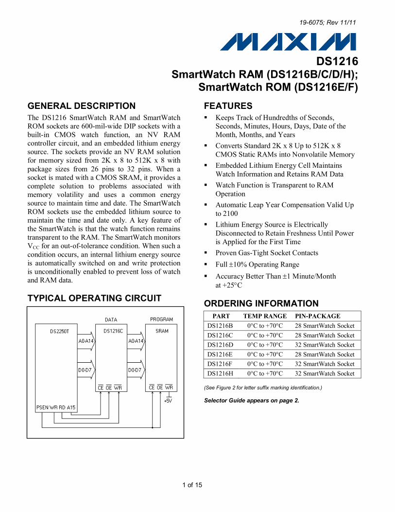
The DS1216 SmartWatch RAM and SmartWatch ROM sockets are 600-mil-wide DIP sockets with a built-in CMOS watch function, an NV RAM controller circuit, and an embedded lithium energy source. The sockets provide an NV RAM solution for memory sized from 2K x 8 to 512K x 8 with package sizes from 26 pins to 32 pins. When a socket is mated with a CMOS SRAM, it provides a complete solution to problems associated with memory volatility and uses a common energy source to maintain time and date. The SmartWatch ROM sockets use the embedded lithium source to maintain the time and date only. A key feature of the SmartWatch is that the watch function remains transparent to the RAM. The SmartWatch monitors VCC for an out-of-tolerance condition. When such a condition occurs, an internal lithium energy source is automatically switched on and write protection is unconditionally enabled to prevent loss of watch and RAM data. TYPICAL OPERATING CIRCUIT
FEATURES Keeps Track of Hundredths of Seconds,
Seconds, Minutes, Hours, Days, Date of the Month, Months, and Years
Converts Standard 2K x 8 Up to 512K x 8 CMOS Static RAMs into Nonvolatile Memory
Embedded Lithium Energy Cell Maintains Watch Information and Retains RAM Data
Watch Function is Transparent to RAM Operation
Automatic Leap Year Compensation Valid Up to 2100
Lithium Energy Source is Electrically Disconnected to Retain Freshness Until Power is Applied for the First Time
Proven Gas-Tight Socket Contacts Full ±10% Operating Range Accuracy Better Than ±1 Minute/Month
at +25°C ORDERING INFORMATION
PART TEMP RANGE PIN-PACKAGE DS1216B 0°C to +70°C 28 SmartWatch Socket DS1216C 0°C to +70°C 28 SmartWatch Socket DS1216D 0°C to +70°C 32 SmartWatch Socket DS1216E 0°C to +70°C 28 SmartWatch Socket DS1216F 0°C to +70°C 32 SmartWatch Socket DS1216H 0°C to +70°C 32 SmartWatch Socket
(See Figure 2 for letter suffix marking identification.)
Selector Guide appears on page 2.
DS1216 SmartWatch RAM (DS1216B/C/D/H);
SmartWatch ROM (DS1216E/F)
19-6075; Rev 11/11
DS1216 SmartWatch RAM/SmartWatch ROM
2 of 15
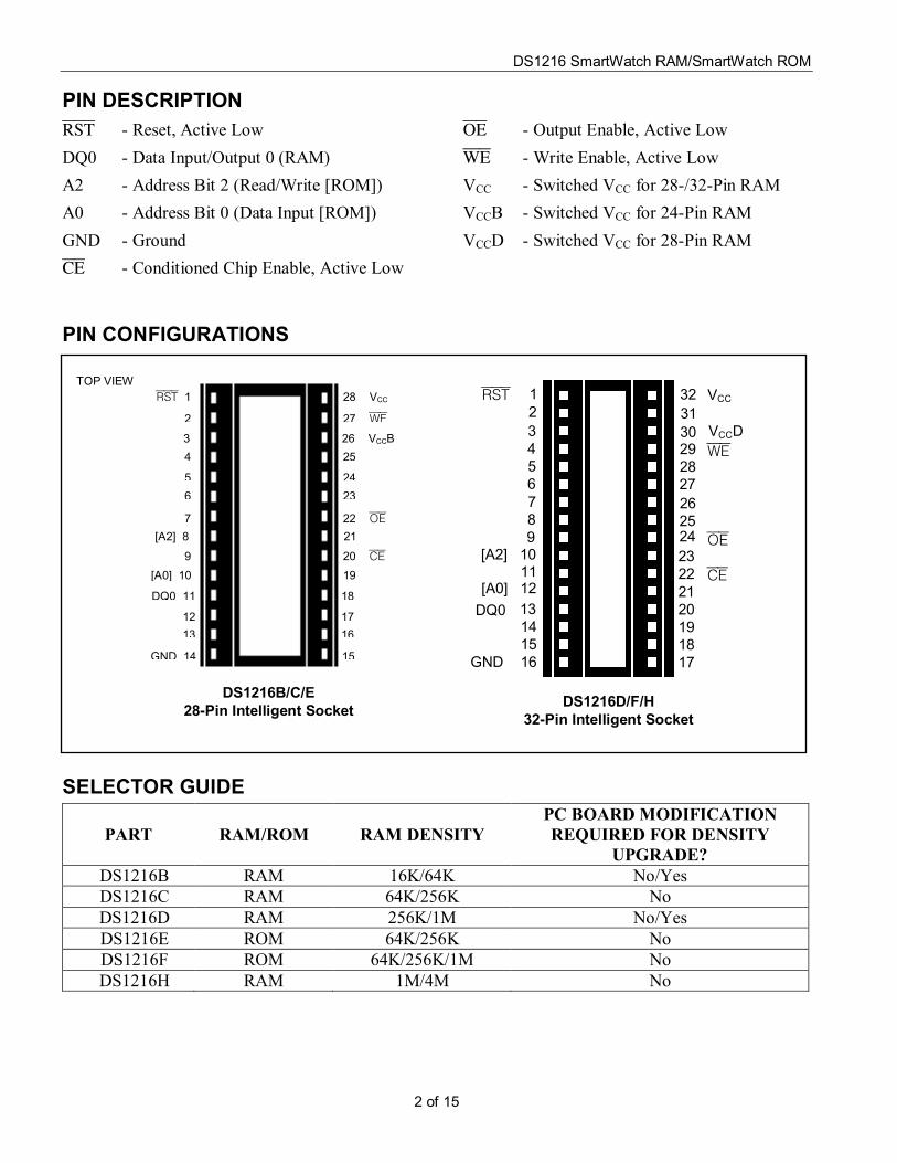
PIN DESCRIPTION RST - Reset, Active Low DQ0 - Data Input/Output 0 (RAM) A2 - Address Bit 2 (Read/Write [ROM]) A0 - Address Bit 0 (Data Input [ROM]) GND - Ground CE - Conditioned Chip Enable, Active Low
OE - Output Enable, Active Low WE - Write Enable, Active Low VCC - Switched VCC for 28-/32-Pin RAM VCCB - Switched VCC for 24-Pin RAM VCCD - Switched VCC for 28-Pin RAM
PIN CONFIGURATIONS SELECTOR GUIDE
PART RAM/ROM RAM DENSITY PC BOARD MODIFICATION REQUIRED FOR DENSITY
UPGRADE? DS1216B RAM 16K/64K No/Yes DS1216C RAM 64K/256K No DS1216D RAM 256K/1M No/Yes DS1216E ROM 64K/256K No DS1216F ROM 64K/256K/1M No DS1216H RAM 1M/4M No
DS1216B/C/E 28-Pin Intelligent Socket
2 27 WE
4 25
5 24
[A2] 8 21
6 23
9 20 CE
7 22 OE
[A0] 10 19
DQ0 11 18
12 17 13 16
GND 14 15
RST 1 28 VCC
3 26 VCCB
TOP VIEW
DS1216D/F/H 32-Pin Intelligent Socket
[A0] 12 DQ0
VCC
WE
OE
CE
1 2 3 4 5 6 7 8 9
[A2] 10 11
13 14 15 16
32 31
29 28 27 26 25 24 23 22 21 20 19 18 17 GND
RST
30 VCCD
DS1216 SmartWatch RAM/SmartWatch ROM
3 of 15
DETAILED DESCRIPTION The DS1216 SmartWatch RAM and SmartWatch ROM Sockets are 600-mil-wide DIP sockets with a built-in CMOS watch function, an NV RAM controller circuit, and an embedded lithium energy source. The sockets provide an NV RAM solution for memory sized from 2K x 8 to 512K x 8 with package sizes from 26 pins to 32 pins. When a socket is mated with a CMOS SRAM, it provides a complete solution to problems associated with memory volatility and uses a common energy source to maintain time and date. The SmartWatch ROM sockets use the embedded lithium source to maintain the time and date only. A key feature of the SmartWatch is that the watch function remains transparent to the RAM. The SmartWatch monitors VCC for an out-of-tolerance condition. When such a condition occurs, an internal lithium energy source is automatically switched on and write protection is unconditionally enabled to prevent loss of watch and RAM data. Using the SmartWatch saves PC board space since the combination of SmartWatch and the mated RAM take up no more area than the memory alone. The SmartWatch uses the VCC, data I/O 0, CE, OE, and WE for RAM and watch control. All other pins are passed straight through to the socket receptacle. The SmartWatch provides timekeeping information including hundredths of seconds, seconds, minutes, hours, days, date, months, and years. The date at the end of the month is automatically adjusted for months with fewer than 31 days, including correction for leap years. The SmartWatch operates in either 24-hour or 12-hour format with an AM/PM indicator. OPERATION Communication with the SmartWatch RAM is established by pattern recognition on a serial bit stream of 64 bits that must be matched by executing 64 consecutive write cycles containing the proper data on DQ0. On the SmartWatch ROM, communication with the clock is established using A2 and A0, and either OE or CE. All accesses that occur prior to recognition of the 64-bit pattern are directed to memory. After the pattern match, the next 64 reads and/or writes are directed to the clock, and the RAM is disabled. Once the pattern is established, the next 64 read/write cycles will be directed to the RTC registers. When power is cycled, 64 reads should be executed prior to any writes to ensure that the RTC registers are not written. A pattern match is ignored if the RST bit is zero and the RST pin goes low during the match sequence. A pattern match is also terminated if a read occurs during the 64-bit match sequence.
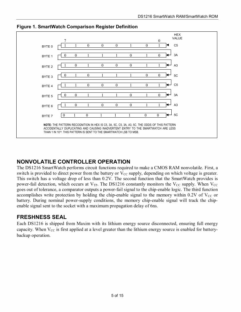
PATTERN MATCH—RAM Data transfer to and from the timekeeping registers is accomplished with a serial bit stream under control of chip enable (CE), output enable (OE), and write enable (WE). Initially, a read cycle to any memory location using the CE and OE control of the SmartWatch starts the pattern recognition sequence by moving a pointer to the first bit of the 64-bit comparison register. Next, 64 consecutive write cycles are executed using the CE and WE control of the SmartWatch. These 64 write cycles are used only to gain access to the SmartWatch. Therefore, any address to the memory in the socket is acceptable. However, the write cycles generated to gain access to the SmartWatch are also writing data to a location in the mated RAM. The preferred way to manage this requirement is to set aside just one address location in RAM as a SmartWatch scratch pad. When the first write cycle is executed, it is compared to bit 0 of the 64-bit comparison register. If a match is found, the pointer increments to the next location of the
DS1216 SmartWatch RAM/SmartWatch ROM
4 of 15
comparison register and awaits the next write cycle. If a match is not found, the pointer does not advance and all subsequent write cycles are ignored. If a read cycle occurs at any time during pattern recognition, the present sequence is aborted and the comparison register pointer is reset. Pattern recognition continues for 64 write cycles as described above until all the bits in the comparison register have been matched (this bit pattern is shown in Figure 1). With a correct match for 64 bits, the SmartWatch is enabled and data transfer to or from the timekeeping registers can proceed. The next 64 cycles will cause the SmartWatch to either receive or transmit data on DQ0, depending on the level of the OE pin or the WE pin. Cycles to other locations outside the memory block can be interleaved with CE cycles without interrupting the pattern recognition sequence or data transfer sequence to the SmartWatch. PATTERN MATCH—ROM Communication with the SmartWatch is established by pattern recognition of a serial bit stream of 64 bits that must be matched by executing 64 consecutive write cycles, placing address bit A2 low with the proper data on address bit A0. The 64 write cycles are used only to gain access to the SmartWatch. Prior to executing the first of 64 write cycles, a read cycle should be executed by holding A2 high. The read cycle will reset the comparison register pointer within the SmartWatch, ensuring the pattern recognition starts with the first bit of the sequence. When the first write cycle is executed, it is compared to bit 0 of the 64-bit comparison register. If a match is found, the pointer increments to the next location of the comparison register and awaits the next write cycle. If a match is not found, the pointer does not advance and all subsequent write cycles are ignored. If a read cycle occurs at any time during pattern recognition, the present sequence is aborted and the comparison register pointer is reset. Pattern recognition continues for a total of 64 write cycles as described above, until all the bits in the comparison register have been matched (this bit pattern is shown in Figure 1). With a correct match for 64 bits, the SmartWatch is enabled and data transfer to or from the timekeeping registers can proceed. The next 64 cycles will cause the SmartWatch to either receive data on data in (A0) or transmit data on data out (DQ0), depending on the level of /WRITE READ (A2). After power-up, the controller could be in the 64-bit clock register read/write sequence (from an incomplete access prior to power-down). Therefore, it is recommended that a 64-bit read be performed upon power-up to prevent accidental writes to the clock, and to prevent reading clock data when access to the RAM would otherwise be expected.
DS1216 SmartWatch RAM/SmartWatch ROM
5 of 15
Figure 1. SmartWatch Comparison Register Definition
NONVOLATILE CONTROLLER OPERATION The DS1216 SmartWatch performs circuit functions required to make a CMOS RAM nonvolatile. First, a switch is provided to direct power from the battery or VCC supply, depending on which voltage is greater. This switch has a voltage drop of less than 0.2V. The second function that the SmartWatch provides is power-fail detection, which occurs at VTP. The DS1216 constantly monitors the VCC supply. When VCC goes out of tolerance, a comparator outputs a power-fail signal to the chip-enable logic. The third function accomplishes write protection by holding the chip-enable signal to the memory within 0.2V of VCC or battery. During nominal power-supply conditions, the memory chip-enable signal will track the chip-enable signal sent to the socket with a maximum propagation delay of 6ns. FRESHNESS SEAL Each DS1216 is shipped from Maxim with its lithium energy source disconnected, ensuring full energy capacity. When VCC is first applied at a level greater than the lithium energy source is enabled for battery-backup operation.
1 1 0 0 0 1 0 1
0 0 1 1 1 0 1 0
1 0 1 0 0 0 1 1
0 1 0 1 1 1 0 0
1 1 0 0 0 1 0 1
0 0 1 1 1 0 1 0
1 0 1 0 0 0 1 1
0 1 0 1 1 1 0 0
BYTE 0
BYTE 1
BYTE 2
BYTE 3
BYTE 4
BYTE 5
BYTE 6
BYTE 7
C5
3A
A3
5C
C5
3A
A3
5C
HEX VALUE
7 0
NOTE: THE PATTERN RECOGNITION IN HEX IS C5, 3A, 5C, C5, 3A, A3, 5C. THE ODDS OF THIS PATTERN ACCIDENTALLY DUPLICATING AND CAUSING INADVERTENT ENTRY TO THE SMARTWATCH ARE LESS THAN 1 IN 1019. THIS PATTERN IS SENT TO THE SMARTWATCH LSB TO MSB.
DS1216 SmartWatch RAM/SmartWatch ROM
6 of 15
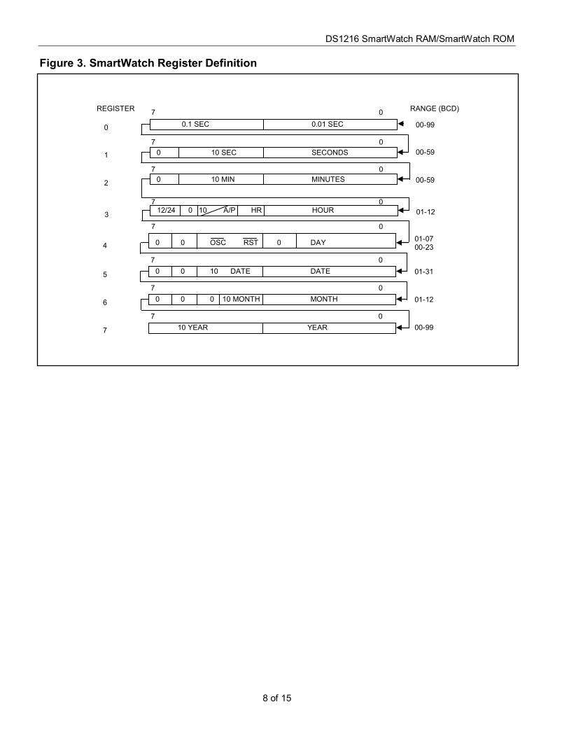
SMARTWATCH REGISTER INFORMATION The SmartWatch information is contained in eight registers of 8 bits, each of which is sequentially accessed one bit at a time after the 64-bit pattern recognition sequence has been completed. When updating the SmartWatch registers, each must be handled in groups of 8 bits. Writing and reading individual bits within a register could produce erroneous results. These read/write registers are defined in Figure 3. Data contained in the SmartWatch registers is in binary-coded decimal (BCD) format. Reading and writing the registers is always accomplished by stepping through all eight registers, starting with bit 0 of register 0 and ending with bit 7 of register 7. AM-PM/12-/24-MODE Bit 7 of the hours register is defined as the 12-hour or 24-hour mode-select bit. When high, the 12-hour mode is selected. In the 12-hour mode, bit 5 is the AM/PM bit with logic high being PM. In the 24-hour mode, bit 5 is the 20-hour bit (20 to 23 hours). OSCILLATOR AND RESET BITS Bits 4 and 5 of the day register are used to control the RST and oscillator functions. Bit 4 controls the RST (pin 1). When the RST bit is set to logic 1, the RST input pin is ignored. When the RST bit is set to logic 0, a low input on the RST pin will cause the SmartWatch to abort data transfer without changing data in the watch registers. Bit 5 controls the oscillator. When set to logic 1, the oscillator is off. When set to logic 0, the oscillator turns on and the watch becomes operational. These bits are shipped from the factory set to logic 1. ZERO BITS Registers 1 to 6 contain one or more bits that always read logic 0. When writing these locations, a logic 1 or 0 is acceptable. ADDITIONAL INFORMATION Refer to Application Note 52: Using the Dallas Phantom Real-Time Clocks (available on our website at www.maxim-ic.com/RTCapps) for information about using regarding optional modifications and the phantom clock contained within the SmartWatch.
DS1216 SmartWatch RAM/SmartWatch ROM
7 of 15
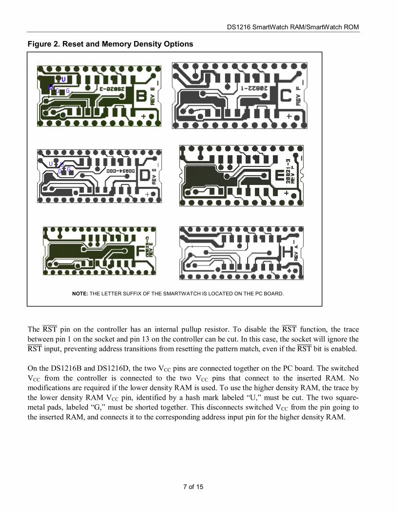
Figure 2. Reset and Memory Density Options
The RST pin on the controller has an internal pullup resistor. To disable the RST function, the trace between pin 1 on the socket and pin 13 on the controller can be cut. In this case, the socket will ignore the RST input, preventing address transitions from resetting the pattern match, even if the RST bit is enabled. On the DS1216B and DS1216D, the two VCC pins are connected together on the PC board. The switched VCC from the controller is connected to the two VCC pins that connect to the inserted RAM. No modifications are required if the lower density RAM is used. To use the higher density RAM, the trace by the lower density RAM VCC pin, identified by a hash mark labeled “U,” must be cut. The two square-metal pads, labeled “G,” must be shorted together. This disconnects switched VCC from the pin going to the inserted RAM, and connects it to the corresponding address input pin for the higher density RAM.
NOTE: THE LETTER SUFFIX OF THE SMARTWATCH IS LOCATED ON THE PC BOARD.
DS1216 SmartWatch RAM/SmartWatch ROM
8 of 15
Figure 3. SmartWatch Register Definition
0 0 10 DATE DATE
0 0 0 10 MONTH MONTH
0 10 MIN MINUTES
0.1 SEC 0.01 SEC
0 10 SEC SECONDS
12/24 0 10 A/P HR HOUR
0 0 OSC RST 0 DAY
10 YEAR YEAR
0
1
2
3
4
5
6
7
00-99
00-59
00-59
01-12
01-07 00-23
01-31
01-12
00-99
RANGE (BCD) REGISTER 7 0
7 0
7 0
7 0
7 0
7 0
7 0
7 0
DS1216 SmartWatch RAM/SmartWatch ROM
9 of 15
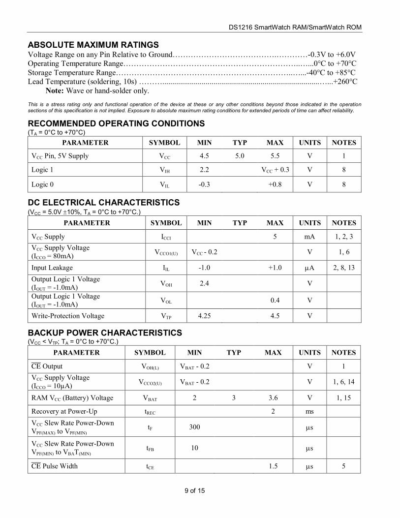
ABSOLUTE MAXIMUM RATINGS Voltage Range on any Pin Relative to Ground………………………………….…………-0.3V to +6.0V Operating Temperature Range…………………………………………………………..…...0°C to +70°C Storage Temperature Range…………………………………………………………..…...-40°C to +85°C Lead Temperature (soldering, 10s) ………................................................................................…...+260°C Note: Wave or hand-solder only.
This is a stress rating only and functional operation of the device at these or any other conditions beyond those indicated in the operation sections of this specification is not implied. Exposure to absolute maximum rating conditions for extended periods of time can affect reliability.
RECOMMENDED OPERATING CONDITIONS (TA = 0°C to +70°C)
PARAMETER SYMBOL MIN TYP MAX UNITS NOTES
VCC Pin, 5V Supply VCC 4.5 5.0 5.5 V 1
Logic 1 VIH 2.2 VCC + 0.3 V 8
Logic 0 VIL -0.3 +0.8 V 8
DC ELECTRICAL CHARACTERISTICS (VCC = 5.0V ±10%, TA = 0°C to +70°C.)
PARAMETER SYMBOL MIN TYP MAX UNITS NOTES
VCC Supply ICCI 5 mA 1, 2, 3 VCC Supply Voltage (ICCO = 80mA) VCCO1(U) VCC - 0.2 V 1, 6
Input Leakage IIL -1.0 +1.0 µA 2, 8, 13 Output Logic 1 Voltage (IOUT = -1.0mA) VOH 2.4 V
Output Logic 1 Voltage (IOUT = -1.0mA) VOL 0.4 V
Write-Protection Voltage VTP 4.25 4.5 V
BACKUP POWER CHARACTERISTICS (VCC < VTP; TA = 0°C to +70°C.)
PARAMETER SYMBOL MIN TYP MAX UNITS NOTES
CE Output VOH(L) VBAT - 0.2 V 1 VCC Supply Voltage (ICCO = 10µA) VCCO2(U) VBAT - 0.2 V 1, 6, 14
RAM VCC (Battery) Voltage VBAT 2 3 3.6 V 1, 15
Recovery at Power-Up tREC 2 ms VCC Slew Rate Power-Down VPF(MAX) to VPF(MIN)
tF 300 µs
VCC Slew Rate Power-Down VPF(MIN) to VBAT(MIN)
tFB 10 µs
CE Pulse Width tCE 1.5 µs 5
DS1216 SmartWatch RAM/SmartWatch ROM
10 of 15
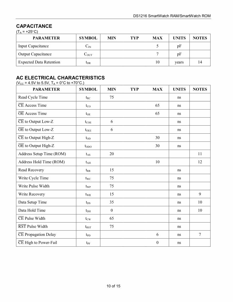
CAPACITANCE (TA = +25°C)
PARAMETER SYMBOL MIN TYP MAX UNITS NOTES
Input Capacitance CIN 5 pF
Output Capacitance COUT 7 pF
Expected Data Retention tDR 10 years 14 AC ELECTRICAL CHARACTERISTICS (VCC = 4.5V to 5.5V, TA = 0°C to +70°C.)
PARAMETER SYMBOL MIN TYP MAX UNITS NOTES
Read Cycle Time tRC 75 ns
CE Access Time tCO 65 ns
OE Access Time tOE 65 ns
CE to Output Low-Z tCOE 6 ns
OE to Output Low-Z tOEE 6 ns
CE to Output High-Z tOD 30 ns
OE to Output High-Z tODO 30 ns
Address Setup Time (ROM) tAS 20 11
Address Hold Time (ROM) tAH 10 12
Read Recovery tRR 15 ns
Write Cycle Time tWC 75 ns
Write Pulse Width tWP 75 ns
Write Recovery tWR 15 ns 9
Data Setup Time tDS 35 ns 10
Data Hold Time tDH 0 ns 10
CE Pulse Width tCW 65 ns
RST Pulse Width tRST 75 ns
CE Propagation Delay tPD 6 ns 7
CE High to Power-Fail tPF 0 ns
DS1216 SmartWatch RAM/SmartWatch ROM
11 of 15
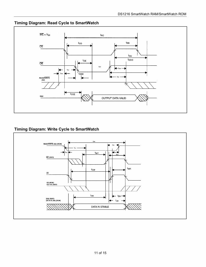
Timing Diagram: Read Cycle to SmartWatch
Timing Diagram: Write Cycle to SmartWatch
DS1216 SmartWatch RAM/SmartWatch ROM
12 of 15
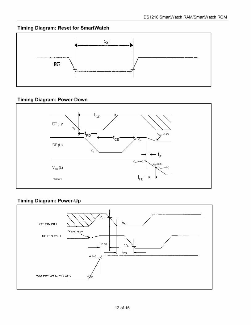
tF
tFB
VBAT(min)VPF(min)
VPF(max)
tCE
tCE
tPD
VIL
VIL
VIH
CE (L)*
CE (U)
VCC (L)
*Note 1
VBAT -0.2V
Timing Diagram: Reset for SmartWatch
Timing Diagram: Power-Down Timing Diagram: Power-Up
DS1216 SmartWatch RAM/SmartWatch ROM
13 of 15
WARNING: Under no circumstances should negative undershoots of any amplitude be allowed when the device is in battery-backup mode. Water washing for flux removal will discharge internal lithium source because exposed voltage pins are present. NOTES: 1) Pin locations are designated “U” when a parameter definition refers to the socket receptacle and “L”
when a parameter definition refers to the socket pin. 2) No memory inserted in the socket. 3) Pin 26L can be connected to VCC or left disconnected at the PC board. 4) SmartWatch sockets can be successfully processed through some conventional wave-soldering
techniques as long as temperature exposure to the lithium energy source contained within does not exceed +85°C. However, post-solder cleaning with water-washing techniques is not permissible. Discharge to the lithium energy source can result, even if deionized water is used. It is equally imperative that ultrasonic vibration is not used in order to avert damage to the quartz crystal resonator employed by the oscillator circuit.
5) tCE max must be met to ensure data integrity on power loss. 6) VCCO1 is the maximum voltage drop from VCC(L) to VCC(U) while Vcc(L) is supplying power. VCCO2
is the maximum voltage drop from VBAT to VCC(U) while the part is in battery backup. 7) Input pulse rise and fall times equal 10ns. 8) Applies to pins RST L, A2 L, A0 L, CE L, OE L, and WE L. 9) tWR is a functions of the latter occurring edge of WE or CE. 10) tDH and tDS are a function of the first occurring edge of WE or CE. 11) tAS is a function of the first occurring edge of OE or CE. 12) tAH is a function of the latter occurring edge of OE or CE. 13) RST (Pin 1) has an internal pullup resistor. 14) Expected data retention is based on using an external SRAM with a data retention current of less than
0.5µA at +25°C. Expected data-retention time (time while on battery) for a given RAM battery current can be calculated using the following formula:
0.045 / (current in amps) = data-retention time in hours
15) The DS1216 products are shipped with the battery-backup power off. First power-up switches backup
battery on to clock and RAM VCC pin upon power-down.
DS1216 SmartWatch RAM/SmartWatch ROM
14 of 15
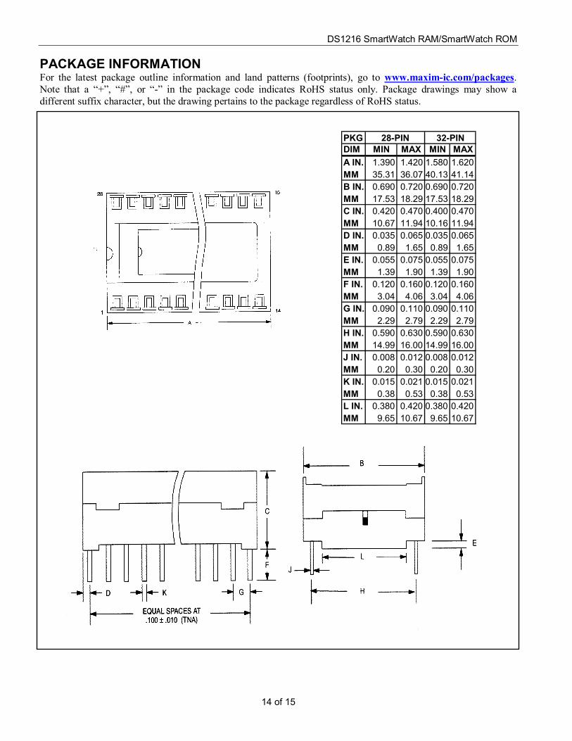
PACKAGE INFORMATION For the latest package outline information and land patterns (footprints), go to www.maxim-ic.com/packages. Note that a “+”, “#”, or “-” in the package code indicates RoHS status only. Package drawings may show a different suffix character, but the drawing pertains to the package regardless of RoHS status.
PKGDIM MIN MAX MIN MAXA IN. 1.390 1.420 1.580 1.620MM 35.31 36.07 40.13 41.14B IN. 0.690 0.720 0.690 0.720MM 17.53 18.29 17.53 18.29C IN. 0.420 0.470 0.400 0.470MM 10.67 11.94 10.16 11.94D IN. 0.035 0.065 0.035 0.065MM 0.89 1.65 0.89 1.65E IN. 0.055 0.075 0.055 0.075MM 1.39 1.90 1.39 1.90F IN. 0.120 0.160 0.120 0.160MM 3.04 4.06 3.04 4.06G IN. 0.090 0.110 0.090 0.110MM 2.29 2.79 2.29 2.79H IN. 0.590 0.630 0.590 0.630MM 14.99 16.00 14.99 16.00J IN. 0.008 0.012 0.008 0.012MM 0.20 0.30 0.20 0.30K IN. 0.015 0.021 0.015 0.021MM 0.38 0.53 0.38 0.53L IN. 0.380 0.420 0.380 0.420MM 9.65 10.67 9.65 10.67
28-PIN 32-PIN
DS1216 SmartWatch RAM/SmartWatch ROM
15 of 15
Maxim cannot assume responsibility for use of any circuitry other than circuitry entirely embodied in a Maxim product. No circuit patent licenses are implied. Maxim reserves the right to change the circuitry and specifications without notice at any time. Maxim I nt egr at ed Product s, 120 San Gabr ie l Dr ive, Sunnyva le, CA 94086 408- 737- 7600 © 2011 Maxim Integrated Products Maxim is a registered trademark of Maxim Integrated Products, Inc.
REVISION HISTORY REVISION
DATE DESCRIPTION PAGES CHANGED
11/11 Updated the Features, Nonvolatile Controller Operation, AM-PM/12-/24-MODE, and Absolute Maximum Ratings sections 1, 5, 6, 9