ds250df230 25-gbps multi-rate 2-channel retimer datasheet
TRANSCRIPT
DS250DF230 25-Gbps Multi-Rate 2-Channel Retimer
1 Features• Dual-channel multi-rate retimer with integrated
signal conditioning• All channels lock independently from 19.6 to
25.8 Gbps (including sub-rates, such as 12.16512 Gbps, 9.8304 Gbps, 6.144 Gbps, and more)
• Ultra-low latency: <500 ps Typical for 25.78125-Gbps data rate
• Adaptive continuous time linear equalizer (CTLE)• Continuous adaptive decision feedback equalizer
(DFE), capable of compensating large channel loss variation over temperature
• Combined equalization supporting 35-dB channel loss at 12.9 GHz
• On-chip eye-opening monitor (EOM), PRBS pattern checker and generator
• Low-jitter transmitter with 3-Tap FIR filter• Integrated 2×2 cross-point• Recovered clock available for system clock
synchronization applications on channel 0• Single power supply, no low-jitter reference clock
required• Wide stay-in-lock temperature range
2 Applications• Jitter cleaning for front-port optical interface in
wireless and wired systems• Backplane/mid-plane reach extension• Active cable assemblies• 802.3bj 100GbE, InfiniBand EDR, and OIF-
CEI-25G-LR/MR/SR/VSR electrical interfaces• SFP28, QSFP28, CFP2/CFP4, CDFP
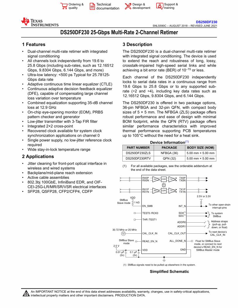
3 DescriptionThe DS250DF230 is a dual-channel multi-rate retimer with integrated signal conditioning. The device is used to extend the reach and robustness of long, lossy, crosstalk-impaired high-speed serial links and while achieving a bit error rate (BER) of 10–15 or less.
Each channel of the DS250DF230 independently locks to serial data rates in a continuous range from 19.6 Gbps to 25.8 Gbps or to any supported sub-rate (÷2 and ÷4), including key data rates such as 12.16512 Gbps, 9.8304 Gbps, and 6.144 Gbps.
The DS250DF230 is offered in two package options, 36-pin NFBGA and 32-pin QFN, with compact body sizes of 5 × 5 mm. The NFBGA (ZLS) package offers robust performance and ease of design with minimal BOM footprint, while the QFN (RTV) package offers similar performance characteristics with improved thermal performance supporting PCB temperatures up to 105°C without the need for a heat sink.
Device Information(1)
PART NUMBER PACKAGE BODY SIZE (NOM)DS250DF230ZLS NFBGA (36) 5.00 mm × 5.00 mm
DS250DF230RTV QFN (32) 5.00 mm × 5.00 mm
(1) For all available packages, see the orderable addendum at the end of the data sheet.
VDD
RX0PRX0N
RX1PRX1N
CAL_CLK_IN CAL_CLK_OUT
ADDR0
ADDR1
TEST0 /RCK0SDC(1)
READ_EN_N ALL_DONE_N
SDA(1)
INT_N
TX0PTX0N
TX1PTX1N
GND
(1) SMBus signals need to be pulled up elsewhere in the system.
30.72 MHz or 25 MHz7RQH[WGHYLFH¶V
CAL_CLK_IN
Float for SMBus Slave
mode, or connect to next
GHYLFH¶V5($'_EN_N for
SMBus Master mode
2.5V or 3.3V
To other open-drain
interrupt pins
VDD
0.01 F
(2x)
0.1 F
(2x)
SMBus Slave
mode
SMBus
Slave mode
2.5 V
RX
EN_SMB
Address straps (pull-up, pull-
down, or float)
1 N
To system
SMBus
CDR TX
RX TX
THR /TEST1
X
CDR
Simplified Schematic
DS250DF230SNLS590C – AUGUST 2018 – REVISED JUNE 2021
An IMPORTANT NOTICE at the end of this data sheet addresses availability, warranty, changes, use in safety-critical applications, intellectual property matters and other important disclaimers. PRODUCTION DATA.

Table of Contents1 Features............................................................................12 Applications..................................................................... 13 Description.......................................................................14 Revision History.............................................................. 25 Description (continued).................................................. 36 Pin Configuration and Functions...................................47 Specifications.................................................................. 7
7.1 Absolute Maximum Ratings ....................................... 77.2 ESD Ratings .............................................................. 77.3 Recommended Operating Conditions ........................77.4 Thermal Information ...................................................87.5 Electrical Characteristics ............................................87.6 Timing Requirements ...............................................147.7 Switching Characteristics .........................................147.8 Typical Characteristics.............................................. 15
8 Detailed Description......................................................168.1 Overview................................................................... 168.2 Functional Block Diagram......................................... 168.3 Feature Description...................................................178.4 Device Functional Modes..........................................28
8.5 Programming............................................................ 308.6 Register Maps...........................................................32
9 Application and Implementation.................................. 929.1 Application Information............................................. 929.2 Typical Applications.................................................. 92
10 Power Supply Recommendations............................10511 Layout.........................................................................106
11.1 Layout Guidelines................................................. 10611.2 Layout Examples...................................................106
12 Device and Documentation Support........................10812.1 Device Support..................................................... 10812.2 Documentation Support........................................ 10812.3 Receiving Notification of Documentation Updates10812.4 Support Resources............................................... 10812.5 Trademarks...........................................................108
13 Electrostatic Discharge Caution.............................. 10814 Glossary..................................................................... 10815 Mechanical, Packaging, and Orderable
Information.................................................................. 108
4 Revision HistoryNOTE: Page numbers for previous revisions may differ from page numbers in the current version.
Changes from Revision B (October 2019) to Revision C (June 2021) Page• Updated the numbering format for tables, figures, and cross-references throughout the document..................1• Added QFN (RTV) package option information.................................................................................................. 1• Added QFN (RTV) pin configuration and functions.............................................................................................4• Added QFN (RTV) thermal information...............................................................................................................8• Added tEQ_Adapt typical value.............................................................................................................................. 8• Added footnotes about bit errors during EQ adaptation and difference in tEQ_ADAPT for lower line rates........... 8• Added Fast CDR Lock Mode section to Detailed Description ......................................................................... 19• Added CDR Status Description to Channel Reg 0x02......................................................................................32
Changes from Revision A (December 2018) to Revision B (October 2019) Page• Initial Public Release.......................................................................................................................................... 1• Changed Channel Reg_0x79[4] definition, marking this as RESERVED......................................................... 32• Changed Channel Reg_0x7E[3:0] definition, marking this as RESERVED......................................................32• Changed Channel Reg_0x7F[5] definition, marking this as RESERVED.........................................................32• Changed Channel Reg_0x8C definition, marking this register as RESERVED............................................... 32• Added expanded Channel Reg_0x95 definition............................................................................................... 32
DS250DF230SNLS590C – AUGUST 2018 – REVISED JUNE 2021 www.ti.com
2 Submit Document Feedback Copyright © 2021 Texas Instruments Incorporated
Product Folder Links: DS250DF230

5 Description (continued)The DS250DF230 has a single power supply and minimal need for external components. These features reduce PCB routing complexity and BOM cost.
The advanced equalization features of the DS250DF230 include a low-jitter 3-tap transmit finite impulse response (FIR) filter, an adaptive continuous-time linear equalizer (CTLE), and an adaptive decision feedback equalizer (DFE). This enables reach extension for lossy interconnect and backplanes with multiple connectors and crosstalk. The integrated CDR function is available for front-port optical module applications to reset the jitter budget and retime the high-speed serial data. The DS250DF230 supplies 2x2 cross-point that gives the host lane crossing, fanout, and multiplexing options.
The DS250DF230 can be configured either through the SMBus or through an external EEPROM. Up to 16 devices can share an EEPROM using common-channel configuration. A non-disruptive on-chip eye monitor and a PRBS generator and checker is available for in-system diagnostics.
www.ti.comDS250DF230
SNLS590C – AUGUST 2018 – REVISED JUNE 2021
Copyright © 2021 Texas Instruments Incorporated Submit Document Feedback 3
Product Folder Links: DS250DF230

6 Pin Configuration and Functions
TX0P TX0N GND GND TX1P TX1N
GND GNDREAD_EN
_N
ALL_DONE
_NGND GND
CAL_CLK
_INTHR/TEST1 VDD VDD SDA
CAL_CLK
_OUT
EN_SMBTEST0/
RCK0VDD VDD SDC ADDR0
GND GND ADDR1 INT_N GND GND
RX0P RX0N GND GND RX1P RX1N
F
E
D
C
B
A
F
E
D
C
B
A
6 5 4 3 2 1
6 5 4 3 2 1
Legend
Control/Status
High-Speed
Ground
Power
Figure 6-1. ZLS Package 36-Pin NFBGA Top View
GN
D
GN
D
GN
D
GN
D
TX
1N
TX
1P
TX
0N
TX
0P
GN
D
GN
D
GN
D
GN
D
RX
1N
RX
1P
RX
0N
RX
0P
12356 4
Thermal Pad (DAP)
78
13
14
12
9
10
11
15
16
2423222019 211817
28
27
29
32
31
30
26
25
ALL_DONE_N
VDD
VDD
INT_N
ADDR0
SDC
SDA
CAL_CLK_IN
READ_EN_N
VDD
THR/TEST1
TEST0/RCK0
VDD
EN_SMB
ADDR1
CAL_CLK_OUT
Figure 6-2. RTV Package 32-Pin QFN Top View
Table 6-1. Pin FunctionsPIN
TYPE
INTERNALPULL-UP/
PULL-DOWN
DESCRIPTIONNAME NFBGA QFN
HIGH-SPEED DIFFERENTIAL I/Os
RX0P A6 18 Input None Inverting and noninverting differential inputs to the equalizer. An on-chip, 100-Ω termination resistor connects RXP to RXN. These inputs must be AC-coupled.RX0N A5 19 Input None
RX1P A2 22 Input None Inverting and noninverting differential inputs to the equalizer. An on-chip, 100-Ω termination resistor connects RXP to RXN. These inputs must be AC-coupled.RX1N A1 23 Input None
TX0P F6 7 Output None Inverting and noninverting 50Ω driver outputs. These outputs must be AC-coupled.TX0N F5 6 Output None
TX1P F2 3 Output None Inverting and noninverting 50Ω driver outputs. These outputs must be AC-coupled.TX1N F1 2 Output None
CALIBRATION CLOCK PINS
CAL_CLK_IN D6 10 Input, 2.5V LVCMOS None
30.72-MHz (±100 PPM), 2.5-V single-ended clock from external oscillator. No stringent phase noise or jitter requirements on this clock. Also supports 25-MHz (±100 PPM) clock by programming the corresponding registers.
CAL_CLK_OUT D1 31 Output, 2.5V LVCMOS None
2.5-V buffered replica of calibration clock input (CAL_CLK_IN) for connecting multiple (up to 20 or more) devices in a daisy-chained fashion.
SYSTEM MANAGEMENT BUS (SMBus) PINS
ADDR0 C1 25 Input, 4-level None 4-level strap pins used to set the SMBus address of the device. The pin state is read on power-up. The multi-level nature of these pins allows for 16 unique device addresses. The four strap options include:0: 1 kΩ to GNDR: 10 kΩ to GNDF: Float1: 1 kΩ to VDDRefer to Section 8.4.3 for more information.
ADDR1 B4 16 Input, 4-level None
DS250DF230SNLS590C – AUGUST 2018 – REVISED JUNE 2021 www.ti.com
4 Submit Document Feedback Copyright © 2021 Texas Instruments Incorporated
Product Folder Links: DS250DF230
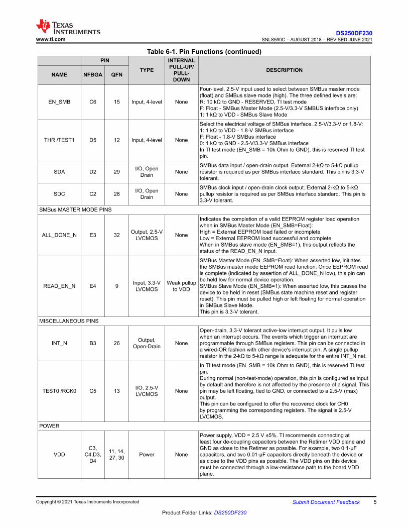
Table 6-1. Pin Functions (continued)PIN
TYPE
INTERNALPULL-UP/
PULL-DOWN
DESCRIPTIONNAME NFBGA QFN
EN_SMB C6 15 Input, 4-level None
Four-level, 2.5-V input used to select between SMBus master mode (float) and SMBus slave mode (high). The three defined levels are:R: 10 kΩ to GND - RESERVED, TI test modeF: Float - SMBus Master Mode (2.5-V/3.3-V SMBUS interface only)1: 1 kΩ to VDD - SMBus Slave Mode
THR /TEST1 D5 12 Input, 4-level None
Select the electrical voltage of SMBus interface. 2.5-V/3.3-V or 1.8-V:1: 1 kΩ to VDD - 1.8-V SMBus interfaceF: Float - 1.8-V SMBus interface0: 1 kΩ to GND - 2.5-V/3.3-V SMBus interfaceIn TI test mode (EN_SMB = 10k Ohm to GND), this is reserved TI test pin.
SDA D2 29 I/O, Open Drain None
SMBus data input / open-drain output. External 2-kΩ to 5-kΩ pullup resistor is required as per SMBus interface standard. This pin is 3.3-V tolerant.
SDC C2 28 I/O, Open Drain None
SMBus clock input / open-drain clock output. External 2-kΩ to 5-kΩ pullup resistor is required as per SMBus interface standard. This pin is 3.3-V tolerant.
SMBus MASTER MODE PINS
ALL_DONE_N E3 32 Output, 2.5-V LVCMOS None
Indicates the completion of a valid EEPROM register load operation when in SMBus Master Mode (EN_SMB=Float):High = External EEPROM load failed or incompleteLow = External EEPROM load successful and completeWhen in SMBus slave mode (EN_SMB=1), this output reflects the status of the READ_EN_N input.
READ_EN_N E4 9 Input, 3.3-V LVCMOS
Weak pullup to VDD
SMBus Master Mode (EN_SMB=Float): When asserted low, initiates the SMBus master mode EEPROM read function. Once EEPROM read is complete (indicated by assertion of ALL_DONE_N low), this pin can be held low for normal device operation.SMBus Slave Mode (EN_SMB=1): When asserted low, this causes the device to be held in reset (SMBus state machine reset and register reset). This pin must be pulled high or left floating for normal operation in SMBus Slave Mode.This pin is 3.3-V tolerant.
MISCELLANEOUS PINS
INT_N B3 26 Output, Open-Drain None
Open-drain, 3.3-V tolerant active-low interrupt output. It pulls low when an interrupt occurs. The events which trigger an interrupt are programmable through SMBus registers. This pin can be connected in a wired-OR fashion with other device's interrupt pin. A single pullup resistor in the 2-kΩ to 5-kΩ range is adequate for the entire INT_N net.
TEST0 /RCK0 C5 13 I/O, 2.5-V LVCMOS None
In TI test mode (EN_SMB = 10k Ohm to GND), this is reserved TI test pin.During normal (non-test-mode) operation, this pin is configured as input by default and therefore is not affected by the presence of a signal. This pin may be left floating, tied to GND, or connected to a 2.5-V (max) output.This pin can be configured to offer the recovered clock for CH0 by programming the corresponding registers. The signal is 2.5-V LVCMOS.
POWER
VDDC3,
C4,D3, D4
11, 14, 27, 30 Power None
Power supply, VDD = 2.5 V ±5%. TI recommends connecting at least four de-coupling capacitors between the Retimer VDD plane and GND as close to the Retimer as possible. For example, two 0.1-µF capacitors, and two 0.01-µF capacitors directly beneath the device or as close to the VDD pins as possible. The VDD pins on this device must be connected through a low-resistance path to the board VDD plane.
www.ti.comDS250DF230
SNLS590C – AUGUST 2018 – REVISED JUNE 2021
Copyright © 2021 Texas Instruments Incorporated Submit Document Feedback 5
Product Folder Links: DS250DF230

Table 6-1. Pin Functions (continued)PIN
TYPE
INTERNALPULL-UP/
PULL-DOWN
DESCRIPTIONNAME NFBGA QFN
GND
A3, A4,B1, B2,B5, B6,E1, E2,E5, E6,F3,
F4
1, 4, 5, 8, 17, 20, 21,
24
Power None
Ground reference. The GND pins on this device must be connected through a low-resistance path to the board GND plane.
DAP — DAP Power NoneDAP is the exposed pad at the bottom of the RTV package. The exposed pad should be connected to the GND plane through a 3x3 via array.
DS250DF230SNLS590C – AUGUST 2018 – REVISED JUNE 2021 www.ti.com
6 Submit Document Feedback Copyright © 2021 Texas Instruments Incorporated
Product Folder Links: DS250DF230
7 Specifications7.1 Absolute Maximum Ratingsover operating free-air temperature range (unless otherwise noted)(1)
MIN MAX UNITVDDABSMAX Supply Voltage, VDD to GND –0.5 2.75 V
VIO2.5V-ABSMAX 2.5V I/O voltage (LVCMOS and Analog) –0.5 2.75 V
VIO3.3V-ABSMAX 3.3V I/O Voltage (SDA, SDC, INT_N, READ_EN) –0.5 4 V
VINABSMAX Signal Input voltage(RXnP, RXnN) –0.5 2.75 V
VOUTABSMAX Signal Output voltage(TXnP, TXnN) –0.5 2.75 V
TJABSMAX Junction Temperature 150 °C
Tstg Storage Temperature range –40 150 °C
(1) Stresses beyond those listed under Absolute Maximum Rating may cause permanent damage to the device. These are stress ratings only, which do not imply functional operation of the device at these or any other conditions beyond those indicated under Recommended Operating Condition. Exposure to absolute-maximum-rated conditions for extended periods may affect device reliability.
7.2 ESD RatingsVALUE UNIT
V(ESD) Electrostatic discharge
Human body model (HBM), per ANSI/ESDA/JEDEC JS-001, all pins(1) ±2000
VCharged device model (CDM), per JEDEC specification JESD22-C101, all pins(2) ±1000
(1) JEDEC document JEP155 states that 500-V HBM allows safe manufacturing with a standard ESD control process.(2) JEDEC document JEP157 states that 250-V CDM allows safe manufacturing with a standard ESD control process.
7.3 Recommended Operating Conditionsover operating free-air temperature range (unless otherwise noted)
MIN NOM MAX UNIT
VDD Supply voltage, VDD to GND.DC plus AC power should not exceed these limits. 2.375 2.5 2.625 V
NVDD Supply noise, DC to <50 Hz, sinusoidal(1) 250 mVpp
NVDD Supply noise, 50 Hz to 10 MHz, sinusoidal(1) 20 mVpp
NVDD Supply noise, >10 MHz, sinusoidal(1) 10 mVpp
Tramp VDD supply ramp time, from 0 V to 2.375 V 150 us
TJ Operating junction temperature –40 110 °C
TA Operating ambient temperature –40 85(2) °C
VIO2.5V 2.5 V LVCMOS 2.375 2.5 2.625 V
VIO3.3V,INT_N Open Drain I/O voltage(INT_N) 3.6 V
VIO3.3V Open Drain I/O voltage(SDA,SDC)(3) 3.6 V
(1) Steps must be taken to ensure the combined AC plus DC noise meets the VDD supply voltage limits.(2) Steps must be taken to ensure the operating junction temperature range and stay-in-lock range (TEMPLOCK+ ,TEMPLOCK-) are met.
Refer to the Electrical Characteristics for more details concerning TEMPLOCK+ and TEMPLOCK-.(3) Set THR pin to select SMBUS electrical voltage
www.ti.comDS250DF230
SNLS590C – AUGUST 2018 – REVISED JUNE 2021
Copyright © 2021 Texas Instruments Incorporated Submit Document Feedback 7
Product Folder Links: DS250DF230

7.4 Thermal Information
THERMAL METRIC(1) CONDITIONS(2)
DS250DF230ZLS DS250DF230RTVUNITZLS (NFBGA) RTV (QFN)
36 PINS 32 PINSRθJA Junction-to-ambient thermal resistance 4-layer JEDEC board 49.3 30.3 °C/W
RθJC(top) Junction-to-case (top) thermal resistance 4-layer JEDEC board 20.7 17.6 °C/W
RθJB Junction-to-board thermal resistance 4-layer JEDEC board 24.5 10.7 °C/W
ΨJT Junction-to-top characterization parameter 4-layer JEDEC board 0.5 0.2 °C/W
ΨJB Junction-to-board characterization parameter 4-layer JEDEC board 24.7 10.6 °C/W
RθJC(bot) Junction-to-case (bot) thermal resistance 4-layer JEDEC board -- 1.8 °C/W
(1) For more information about traditional and new thermal metrics, see the Semiconductor and IC Package Thermal Metrics application report.
(2) No heat sink or airflow was assumed for these estimations. Depending on the application, a heat sink, faster airflow, and/or reduced ambient temperature (<85 C) may be required in order to meet the maximum junction temperature specification per the Recommended Operating Conditions.
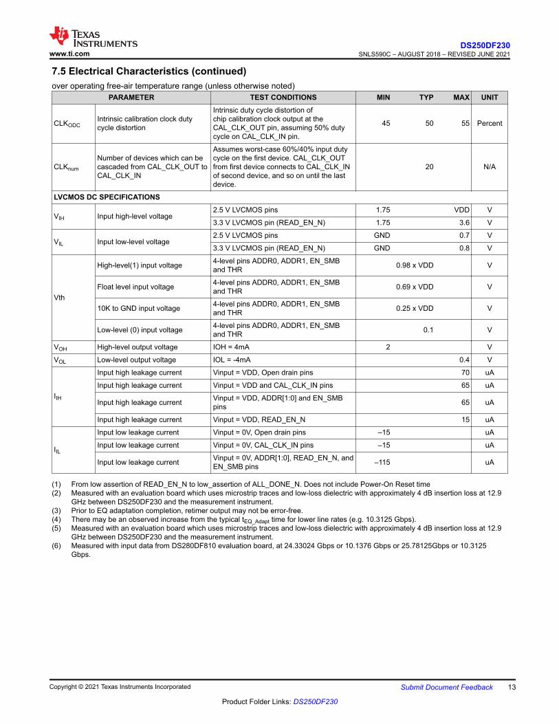
7.5 Electrical Characteristics over operating free-air temperature range (unless otherwise noted)
PARAMETER TEST CONDITIONS MIN TYP MAX UNITPOWER CONSUMPTION
WChannelPower Consumption Per Active Channel
Active mode with CTLE, Tx FIR, full DFE and Crosspoint enabled. Idle power consumption not included.
256 347 mW
Active mode with CTLE, Tx FIR, and full DFE enabled. Crosspoint disabled. Idle power consumption not included.
248 mW
Active mode with CTLE, Tx FIR, and partial DFE enabled(taps 1-2 only). Crosspoint and DFE taps 3-5 disabled. Idle power consumption not included.
235 mW
Active mode with CTLE, and Tx FIR enabled. DFE and crosspoint disabled. Idle power consumption not included.
226 mW
Assuming CDR acquiring lock with CTLE, full DFE, Tx FIR, Driver, and Crosspoint enabled. Idle power consumption not included.
380 445 mW
Assuming CDR acquiring lock with CTLE, full DFE, Tx FIR, Driver, and Crosspoint disabled. Idle power consumption not included.
333 mW
WPRBS
PRBS Checker Power Consumption only Per Channel 200 mW
PRBS Generator Power Consumption only Per Channel 190 mW
WStatic_Total Total Idle Power ConsumptionIdle/Static mode. Power supplied, no high-speed data present at inputs, channel automatically powered down.
165 mW
IStatic_TotalIdle mode total device supply current consumption
Idle/Static mode. Power supplied, no high-speed data present at inputs, channel automatically powered down.
66 100 mA
DS250DF230SNLS590C – AUGUST 2018 – REVISED JUNE 2021 www.ti.com
8 Submit Document Feedback Copyright © 2021 Texas Instruments Incorporated
Product Folder Links: DS250DF230
7.5 Electrical Characteristics (continued)over operating free-air temperature range (unless otherwise noted)
PARAMETER TEST CONDITIONS MIN TYP MAX UNIT
ITotalActive Mode Total Device Supply Current Consumption
Active mode with CTLE, Tx FIR, full DFE and Crosspoint enabled. 271 361 mA
Active mode with CTLE, Tx FIR, and full DFE enabled. Crosspoint disabled. 265 mA
Active mode with CTLE, Tx FIR, and partial DFE enabled(taps 1-2 only). Crosspoint and DFE taps 3-5 disabled.
255 mA
Active mode with CTLE, and Tx FIR enabled. DFE and crosspoint disabled. 247 mA
GENERAL DEVICE-LEVEL SPECIFICATIONS
Rbaud Supported input data rate
Full-rate (divide-by-1) mode of operation. 19.6 25.8 Gbps
Half-rate (divide-by-2) mode of operation. 9.8 12.9 Gbps
Quarter-rate (divide-by-4) mode of operation. 4.9 6.45 Gbps
tEEPROM
EEPROM configuration load time
Single device reading its configuration from an EEPROM. Common channel configuration. This time scales with the number of devices reading from the same EEPROM.
15(1) ms
EEPROM configuration load time
Single device reading its configuration from an EEPROM. Unique-channel configuration. This time scales with the number of devices reading from the same EEPROM.
40(1) ms
tPOR Power-on reset assertion-time
Internal power-on reset (PoR) stretch between stable power supply and de-assertion of internal PoR. The SMBus address is latched on the completion of the PoR stretch, and SMBus accesses are permitted.
50 ms
HIGH-SPEED DIFFERENTIAL OUTPUTS (TXnP, TXnN)
VOD
Output differential voltage amplitude
Measured with c(0)=4 setting (REG_0x3D[6:0]=0x04, REG_0x3E[6:0]=0x40, REG_0x3F[6:0]=0x40). Differential measurement using an 8T pattern (eight 1s followed by eight 0s) at 25.78125 Gbps with TXPn and TXNn terminated by 50 Ohms to GND.
392 mVppd
Output differential voltage amplitude
Measured with c(0)=31 setting (REG_0x3D[6:0]=0x1F, REG_0x3E[6:0]=0x40, REG_0x3F[6:0]=0x40). Differential measurement using an 8T pattern (eight 1s followed by eight 0s) at 25.78125 Gbps with TXPn and TXNn terminated by 50 Ohms to GND.
1195 mVppd
VOD_Raw_L
Output differential voltage amplitude under Raw Mode, low swing setting
Raw Mode(CDR Bypassed), low swing setting(REG_0xD[0]=0), differential measurement using 8T pattern(eight 1s followed by eight 0s) at 25.78125Gbps and 9.8304Gbps with TXPn and TXNn terminated by 50 Ohms to GND.RPH=REG_0x1A[7:6]=0
602 mVppd
www.ti.comDS250DF230
SNLS590C – AUGUST 2018 – REVISED JUNE 2021
Copyright © 2021 Texas Instruments Incorporated Submit Document Feedback 9
Product Folder Links: DS250DF230

7.5 Electrical Characteristics (continued)over operating free-air temperature range (unless otherwise noted)
PARAMETER TEST CONDITIONS MIN TYP MAX UNIT
VOD_Raw_H
Output differential voltage amplitude under Raw Mode, high swing setting
Raw Mode(CDR Bypassed), high swing setting(REG_0xD[0]=1),,differential measurement using 8T pattern(eight 1s followed by eight 0s) at 25.78125Gbps and 9.8304Gbps with TXPn and TXNn terminated by 50 Ohms to GND.RPH=REG_0x1A[7:6]=0x3
919 mVppd
VOD_IdleDifferential output amplitude with TX disabled 6.1 mVppd
Vcm_TX DC common-mode output voltage
With respect to signal ground. Measured using an 8T pattern (eight 1s followed by eight 0s) at 25.78125 Gbps with TXPn and TXNn terminated by 50 Ohms to GND. Measured for c(-1)=c(1)=0 and VOD settings in the range of 600 mVppd to 1200 mVppd.
1.01 V
Vcm_TX_AC Common-mode AC output noiseWith respect to signal ground. Measured with PRBS9 data pattern. Measured with a 33GHz (-3dB) low-pass filter.
7.4 mV, RMS
tr, tf
Output transition-time
20%-to-80% rise time and 80%-to-20% fall time on a clock-like 11111 00000 data pattern at 25.78125 Gbps. Measured for ~750 mVppd output amplitude and no equalization: REG_0x3D=+13, REG_0x3E=0, REG_0x3F=0
17.5 ps
Output transition-time, Low slew rate setting
Slow slew rate setting(REG_0x3D[5]=1), 20%-to-80% rise time and 80%-to-20% fall time on a clock-like 11111 00000 data pattern at 9.8304 Gbps. Measured for ~750 mVppd output amplitude and no equalization: REG_0x3D=+13, REG_0x3E=0, REG_0x3F=0
24 ps
RLSDD22
Differential output return loss, SDD22(2) Between 50 MHz and 5 GHz -15.9 dB
Differential output return loss, SDD22(2) Between 5 GHz and 12.9 GHz -13 dB
RLSCD22Differential to common-mode output return loss, SCD22(2) Between 50 MHz and 12.9 GHz -24 dB
RLSDC22Common-mode to differential output return loss, SDC22(2) Between 50 MHz and 12.9 GHz -24 dB
RLSCC22
Common-mode output return loss, SCC22(2) Between 50 MHz and 10 GHz -8 dB
Common-mode output return loss, SCC22(2) Between 10 GHz and 12.9 GHz -8.5 dB
RETIMER TIMING SPECIFICATIONS
tDInput-to-output latency (propagation delay) through a channel
No Crosspoint; CDR enabled and locked. 4.5 UI + 175 ps ps
Crosspoint enabled; CDR enabled and locked.
4.5 UI + 220 ps ps
No crosspoint; CDR in raw mode. 140 ps
tD_V Variation of Input-to-output latency Crosspoint enabled; CDR enabled and locked. ± 50 ps
tSK Channel-to-channel interpair skew Latency difference between channels at full-rate. 30 ps
DS250DF230SNLS590C – AUGUST 2018 – REVISED JUNE 2021 www.ti.com
10 Submit Document Feedback Copyright © 2021 Texas Instruments Incorporated
Product Folder Links: DS250DF230

7.5 Electrical Characteristics (continued)over operating free-air temperature range (unless otherwise noted)
PARAMETER TEST CONDITIONS MIN TYP MAX UNIT
tLock
CDR lock acquisition-time, Normal Lock Mode
Measured at 25.78125 Gbps, Adapt mode 2(REG_0x31[6:5]=0x2) <100 ms
CDR lock acquisition-time, Fast Lock Mode
Measured at 25.78125 Gbps, Adapt mode 2 (REG_0x31[6:5]=0x2). Fast Lock Mode Enabled (REG_0xAC[7] = 1). Adaptation process still runs to find the best CTLE/DFE values after CDR lock is declared.
<10 ms
CDR lock acquisition-time, Fast Lock Mode
Measured at 25.78125 Gbps, Adapt mode 0 (Reg_0x31[6:5]=0x0), Fast Lock Mode Enabled (REG_0xAC[7] = 1). Adaptation process still runs to find the best CTLE/DFE values after CDR lock is declared.
<2 ms
tEQ_AdaptTotal EQ Adaptation Completion Time (includes tLOCK)
Measured at 25.78125 Gbps, Adapt mode 2 (REG_0x31[6:5]=0x2) (3) (4) <3 s
RETIMER JITTER SPECIFICATIONS
JTJ Output Total jitter (TJ)
Measured at 25.78125 Gbps to a probability level of 1E-12 with PRBS11 data pattern an evaluation board traces de-embedded
0.16 UIpp @ 1E-12
JRJ Output Random Jitter (RJ)
Measured at 25.78125 Gbps to a probability level of 1E-12 with PRBS11 data pattern an evaluation board traces de-embedded
6.8 mUI RMS
JDCDOutput Duty Cycle Distortion (DCD)
Measured at 25.78125 Gbps to a probability level of 1E-12 with PRBS11 data pattern an evaluation board traces de-embedded
3.7 mUIpp
HIGH-SPEED DIFFERENTIAL INPUTS (RXnP, RXnN)
VIDMaxMaximum tolerable input differential voltage For normal operation 1200 mVppd
Vcm-SelfSelf-generated input common mode 1.79 V
RLSDD11
Differential input return loss, SDD11(5) Between 50 MHz and 3.69 GHz -20 dB
Differential input return loss, SDD11(5) Between 3.69 GHz and 12.9 GHz -13 dB
RLSDC11Common-mode to differential input return loss, SDC11(5) Between 50 MHz and 12.9 GHz -23 dB
RLSCD11Differential to common-mode input return loss, SCD11(5) Between 50 MHz and 12.9 GHz -23 dB
RLSCC11
Common-mode input return loss, SCC11(5) Between 150 MHz and 10 GHz -11 dB
Common-mode input return loss, SCC11(5) Between 10 GHz and 12.9 GHz -8 dB
VSDATAC signal detect assert (ON) threshold level
Minimum input peak-to-peak amplitude level at device pins required to assert signal detect. Assumes default assert threshold setting. Measured at 25.78125 Gbps with PRBS7.
145 mVppd
VSDDTAC signal detect de-assert (OFF) threshold level
Maximum input peak-to-peak amplitude level at device pins which causes signal detect to de-assert. Assumes default de-assert threshold setting . Measured at 25.78125 Gbps with PRBS7.
84 mVppd
www.ti.comDS250DF230
SNLS590C – AUGUST 2018 – REVISED JUNE 2021
Copyright © 2021 Texas Instruments Incorporated Submit Document Feedback 11
Product Folder Links: DS250DF230

7.5 Electrical Characteristics (continued)over operating free-air temperature range (unless otherwise noted)
PARAMETER TEST CONDITIONS MIN TYP MAX UNITRETIMER CLOCK AND DATA RECOVERY SPECIFICATIONS
BWPLL
PLL bandwidth Measured at 9.8304 Gbps with PRBS7 data pattern 4 MHz
PLL bandwidth Measured at 25.78125 Gbps with PRBS7 data pattern 4.7 MHz
JPEAK
Jitter peaking Measured at 9.8304 Gbps with PRBS7 data pattern. 0.5 dB
Jitter peaking Measured at 25.78125 Gbps with PRBS7 data pattern. 0.5 dB
JTOL
Input jitter tolerance
Measured at25.78125 Gbps with SJ frequency = 190 KHz, 30dB input channel loss, PRBS31 data pattern, ~800 mVppd launch amplitude, and 0.18 UIpp total uncorrelated output jitter in addition to the applied SJ. BER < 1E-12.
9 UIpp
Input jitter tolerance
Measured at 25.78125 Gbps with SJ frequency = 940 KHz, 30dB input channel loss, PRBS31 data pattern, ~800 mVppd launch amplitude, and 0.18 UIpp total uncorrelated output jitter in addition to the applied SJ. BER < 1E-12.
1 UIpp
Input jitter tolerance
Measured at 25.78125 Gbps with SJ frequency > 15MHz, 30dB input channel loss, PRBS31 data pattern, ~800 mVppd launch amplitude, and 0.18 UIpp total uncorrelated output jitter in addition to the applied SJ. BER < 1E-12.
0.33 UIpp
TEMPLOCK-
CDR stay-in-lock junction temperature range, negative ramp. Maximum junction temperature change below initial CDR lock acquisition temperature
110 °C junction temperature starting, ramp rate -3°C/minute, 12 layer PCB 150 °C
TEMPLOCK+
CDR stay-in-lock junction temperature range, positive ramp. Maximum junction temperature change above initial CDR lock acquisition temperature
-40 °C junction temperature starting, ramp rate +3°C/minute, 12 layer PCB 150 °C
RECOVERED CLOCK SPECIFICATIONS
RCKf
Recovered Clock frequency on RCK0 pin
Measured with input data rate as 24.33024 Gbps or 12.16512 Gbps or 10.1376 Gbps 9.8304 Gbps or 6.144 Gbps or 4.9152 Gbps
30.72 MHz
Recovered Clock frequency on RCK0 pin
Measured with input data rate as 25.78125Gbps or 10.3125Gbps 32.2265625 MHz
RCKPhaseRCKf Phase Noise Performance(6)
<=100 Hz < -59 dBc/Hz
Between 100 Hz and 1 kHz < -84 dBc/Hz
Between 1 kHz and 10 kHz < -103 dBc/Hz
>10 kHz < -122 dBc/Hz
CALIBRATION CLOCK SPECIFICATIONS
CLKfCalibration clock frequency Option 1: 30.72 MHz 30.72 MHz
Calibration clock frequency Option 2: 25 MHz 25 MHz
CLKppm Calibration clock PPM tolerance -100 100 PPM
CLKIDC Calibration clock input duty cycle 40 50 60 Percent
DS250DF230SNLS590C – AUGUST 2018 – REVISED JUNE 2021 www.ti.com
12 Submit Document Feedback Copyright © 2021 Texas Instruments Incorporated
Product Folder Links: DS250DF230
7.5 Electrical Characteristics (continued)over operating free-air temperature range (unless otherwise noted)
PARAMETER TEST CONDITIONS MIN TYP MAX UNIT
CLKODCIntrinsic calibration clock duty cycle distortion
Intrinsic duty cycle distortion of chip calibration clock output at the CAL_CLK_OUT pin, assuming 50% duty cycle on CAL_CLK_IN pin.
45 50 55 Percent
CLKnum
Number of devices which can be cascaded from CAL_CLK_OUT to CAL_CLK_IN
Assumes worst-case 60%/40% input duty cycle on the first device. CAL_CLK_OUT from first device connects to CAL_CLK_IN of second device, and so on until the last device.
20 N/A
LVCMOS DC SPECIFICATIONS
VIH Input high-level voltage2.5 V LVCMOS pins 1.75 VDD V
3.3 V LVCMOS pin (READ_EN_N) 1.75 3.6 V
VIL Input low-level voltage2.5 V LVCMOS pins GND 0.7 V
3.3 V LVCMOS pin (READ_EN_N) GND 0.8 V
Vth
High-level(1) input voltage 4-level pins ADDR0, ADDR1, EN_SMB and THR 0.98 x VDD V
Float level input voltage 4-level pins ADDR0, ADDR1, EN_SMB and THR 0.69 x VDD V
10K to GND input voltage 4-level pins ADDR0, ADDR1, EN_SMB and THR 0.25 x VDD V
Low-level (0) input voltage 4-level pins ADDR0, ADDR1, EN_SMB and THR 0.1 V
VOH High-level output voltage IOH = 4mA 2 V
VOL Low-level output voltage IOL = -4mA 0.4 V
IIH
Input high leakage current Vinput = VDD, Open drain pins 70 uA
Input high leakage current Vinput = VDD and CAL_CLK_IN pins 65 uA
Input high leakage current Vinput = VDD, ADDR[1:0] and EN_SMB pins 65 uA
Input high leakage current Vinput = VDD, READ_EN_N 15 uA
IIL
Input low leakage current Vinput = 0V, Open drain pins –15 uA
Input low leakage current Vinput = 0V, CAL_CLK_IN pins –15 uA
Input low leakage current Vinput = 0V, ADDR[1:0], READ_EN_N, and EN_SMB pins –115 uA
(1) From low assertion of READ_EN_N to low_assertion of ALL_DONE_N. Does not include Power-On Reset time(2) Measured with an evaluation board which uses microstrip traces and low-loss dielectric with approximately 4 dB insertion loss at 12.9
GHz between DS250DF230 and the measurement instrument.(3) Prior to EQ adaptation completion, retimer output may not be error-free.(4) There may be an observed increase from the typical tEQ_Adapt time for lower line rates (e.g. 10.3125 Gbps).(5) Measured with an evaluation board which uses microstrip traces and low-loss dielectric with approximately 4 dB insertion loss at 12.9
GHz between DS250DF230 and the measurement instrument.(6) Measured with input data from DS280DF810 evaluation board, at 24.33024 Gbps or 10.1376 Gbps or 25.78125Gbps or 10.3125
Gbps.
www.ti.comDS250DF230
SNLS590C – AUGUST 2018 – REVISED JUNE 2021
Copyright © 2021 Texas Instruments Incorporated Submit Document Feedback 13
Product Folder Links: DS250DF230

7.6 Timing RequirementsPARAMETER TEST CONDITIONS MIN NOM MAX UNIT
SMBus ELECTRICAL CHARACTERISTICS (SLAVE MODE)
VIHInput high-level voltage1.8 V SMBUS Interface SDA and SDC 1.35 3.6 V
VIHInput high-level voltage2.5 V/3.3 V SMBUS Interface SDA and SDC 1.75 3.6 V
VIL Input low-level voltage SDA and SDC GND 0.8 V
CIN Input pin capacitance 2 pF
VOL Low-level output voltage SDA or SDC or INT, IOL = 1.25 mA 0.4 V
IIN Input current SDA or SDC, VINPUT = VIN, VDD, GND –15 15 uA
TR SDA rise time, read operation Pull up resistor = 1 kΩ, Cb = 50pF 150 ns
TF SDA fall time, read operation Pull up resistor = 1 kΩ, Cb = 50pF 4.5 ns
RECOMMENDED SMBus SWITCHING CHARACTERISTICS (SLAVE MODE)fSDC SDC clock frequency 10 100 400 kHz
tHD_DAT Data hold time 0.75 ns
tSU_DAT Data setup time 100 ns
7.7 Switching CharacteristicsPARAMETER TEST CONDITIONS MIN NOM MAX UNIT
SMBus SWITCHING CHARACTERISTICS (2.5 V and 3.3 V MASTER MODE)fSDC SDC clock frequency 260 303 346 kHz
TLOW SDC low period 1.90 µs
THIGH SDC high period 1.40 µs
THD_STA Hold time start operation 1.3 µs
TSU_STA Setup time start operation 1.3 µs
THD_DAT Data hold time 0.5 µs
TSD-DAT Data setup time 1.3 µs
TSU_STO Stop condition setup time 1.4 µs
TBUF Bus free time between Stop-Start 1.8 µs
TR SDC rise time Pull up resistor = 1 kΩ 70 ns
TF SDC fall time Pull up resistor = 1 kΩ 8 ns
DS250DF230SNLS590C – AUGUST 2018 – REVISED JUNE 2021 www.ti.com
14 Submit Document Feedback Copyright © 2021 Texas Instruments Incorporated
Product Folder Links: DS250DF230

7.8 Typical Characteristics
Temperature(°C)
Sle
w R
ate
(ps)
-50 -30 -10 10 30 50 70 90 11015
15.5
16
16.5
17
17.5
18
18.5
19
19.5
20
20.5
21
D001
C(0) = 7C(0) = 16C(0) = 31
Figure 7-1. Output Transition-time vs Ambient Temperature
Temperature(°C)
VO
D (
Vppd)
-50 -30 -10 10 30 50 70 90 1100.4
0.5
0.6
0.7
0.8
0.9
1
1.1
1.2
1.3
1.4
1.5
D001
C(0) = 7C(0) = 16C(0) = 31
Figure 7-2. Typical VOD vs Ambient Temperature
Main Cursor C(0)
VO
D (
Vppd)
3 6 9 12 15 18 21 24 27 300.2
0.4
0.6
0.8
1
1.2
1.4
D001
T = 85°C, VDD = 2.65VT = 85°C, VDD = 2.35VT = -40°C, VDD = 2.65VT = -40°C, VDD = 2.35V
Figure 7-3. Typical VOD vs FIR Main-CursorTemperature °C
Outp
ut Jitte
rA
mplit
ude (
UIp
p)
-40 -25 -10 5 20 35 50 65 80 950.03
0.06
0.09
0.12
0.15
0.18
0.21
0.24
D001
TJ, VDD = 2.35 VDJ, VDD = 2.35 VTJ, VDD = 2.65 VDJ, VDD = 2.65 V
Figure 7-4. Typical Output Jitter vs Ambient Temperature at 25.78125 Gbps
Frequency(MHz)
Inp
ut
Jitte
r A
mplit
ud
e (
UIp
p)
0 0.1 0.2 0.3 0.4 0.5 0.6 0.7 0.8 0.9 10
2
4
6
8
10
12
14
16
18
D001
T = 95 °C, VDD = 2.35VT = 95 °C, VDD = 2.65VT = -40 °C, VDD = 2.35VT = -40 °C, VDD = 2.65V
0.1 MHz to 1 MHz Input Random Jitter = 0.078 UIpp
Figure 7-5. Typical Sinusoidal Input Jitter Tolerance for 30-dB Channel at 25.78125 Gbps
Frequency(MHz)
Input Jitte
r A
mplit
ude (
UIp
p)
1 11 21 31 41 51 61 71 81 91 1000.2
0.3
0.4
0.5
0.6
0.7
0.8
0.9
1
1.1
1.2
1.3
1.4
D001
T = 95 °C, VDD = 2.35VT = 95 °C, VDD = 2.65VT = -40 °C, VDD = 2.35VT = -40 °C, VDD = 2.65V
1 MHz to 100 MHz Input Random Jitter = 0.078 UIpp
Figure 7-6. Typical Input Jitter Tolerance for 30-dB Channel at 25.78125 Gbps
www.ti.comDS250DF230
SNLS590C – AUGUST 2018 – REVISED JUNE 2021
Copyright © 2021 Texas Instruments Incorporated Submit Document Feedback 15
Product Folder Links: DS250DF230

8 Detailed Description8.1 OverviewThe DS250DF230 is a dual-channel multi-rate retimer with integrated signal conditioning. Each of the two channels operates independently. Each channel includes a continuous-time linear equalizer (CTLE) and a Decision Feedback Equalizer (DFE), which together compensate for the presence of a dispersive transmission channel between the source transmitter and the DS250DF230 receiver. The CTLE and DFE are self-adaptive.
Each channel includes an independent voltage-controlled oscillator (VCO) and phase-locked loop (PLL) which produce a clean clock that is frequency-locked to the clock embedded in the input data stream. The high-frequency jitter on the incoming data is attenuated by the PLL, producing a clean clock with substantially reduced jitter. This clean clock is used to re-time the incoming data, removing high-frequency jitter from the data stream and reproducing the data on the output with significantly reduced jitter.
Each channel of the DS250DF230 features an output driver with adjustable differential output voltage and output equalization in the form of a three-tap finite impulse response (FIR) filter. The output FIR compensates for dispersion in the transmission channel at the output of the DS250DF230.
A full 2x2 cross-point switch is integrated inside. This allows multiplexing and de-multiplexing/fanout applications for fail-over redundancy, as well as cross-over applications to aid PCB routing.
Each channel also includes diagnostic features such as a Pseudo-Random Bit Sequence (PRBS) pattern generator and checker, as well as a non-destructive, eye-opening monitor (EOM). The EOM can be used to plot the post-equalized eye at the input to the decision slicer or simply to read the horizontal eye opening (HEO) and vertical eye opening (VEO).
The DS250DF230 is configurable through a single SMBus port. The DS250DF230 can also act as an SMBus master to configure itself from an external EEPROM. Up to sixteen DS250DF230 devices can share a single SMBus.
The sections which follow describe the functionality of various circuits and features within the DS250DF230. For more information about how to program or operate these features, consult the DS250DF230 Programmer's Guide (SNLU182).
8.2 Functional Block Diagram
RXnP
RXnNCTLE+VGA + Sampler
DFE
TX FIR
Raw
Retimed
PRBS Gen
PFD, CDR,
and Divider
VCO
PRBS
DriverTXnP
TXnN
Channel Digital Core
CAL_CLK_IN CAL_CLK_OUT
Shared Digital CorePower-On
Reset
Always-On
10MHz
PRBS
Checker
Eye
Monitor
Signal
Detect
SCL
SDA
READ_EN_N ALL_DONE_N
INT_N
Voltage
Regulator
Voltage
Regulator
EN_SMB
One of two channels
ADDRn
Buffer
X-
point
To adjacent
channel
Shared Digital Core
Term
DS250DF230SNLS590C – AUGUST 2018 – REVISED JUNE 2021 www.ti.com
16 Submit Document Feedback Copyright © 2021 Texas Instruments Incorporated
Product Folder Links: DS250DF230

8.3 Feature Description8.3.1 Device Data Path Operation
The DS250DF230 data path consists of several key blocks as shown in the functional block diagram. These key circuits are:
• Signal Detect• Continuous Time Linear Equalizer (CTLE)• Variable Gain Amplifier (VGA)• Cross-Point Switch• Decision Feedback Equalizer (DFE)• Clock and Data Recovery (CDR)• Calibration Clock• Differential Driver With FIR Filter
8.3.2 Signal Detect
The DS250DF230 receiver contains a signal detect circuit. The signal detect circuit monitors the energy level on the receiver inputs and powers on or off the rest of the high-speed data path if a signal is detected or not. By default, each channel allows the signal detect circuit to automatically power on or off the rest of the high-speed data path depending on the presence of an input signal. The signal detect block can be manually controlled in the SMBus channel registers. This can be useful if it is desired to manually force channels to be disabled. For information on how to manually operate the signal detect circuit, refer to the DS250DF230 Programmer's Guide (SNLU182).
8.3.3 Continuous Time Linear Equalizer (CTLE)
The CTLE in the DS250DF230 is a fully-adaptive equalizer. The CTLE adapts according to a Figure of Merit (FOM) calculation during the lock acquisition process. The FOM calculation is based upon the horizontal eye opening (HEO) and vertical eye opening (VEO). Once the CDR locks and the CTLE adapts, the CTLE boost level is frozen until a manual re-adapt command is issued or until the CDR re-enters the lock acquisition state. The CTLE can be re-adapted by resetting the CDR.
The CTLE consists of 4 stages, with each stage having 2-bit boost control. This allows for many boost combinations, including bypassing the first three stages EQs. The CTLE adaption algorithm allows the CTLE to adapt through 20 of these boost combinations. These 20 boost combinations comprise the EQ Table in the channel registers. See channel registers 0x40 through 0x53.
The boost levels can be set between approximately 0 dB and 25 dB (at 12.89 GHz.)
8.3.4 Variable Gain Amplifier (VGA)
The DS250DF230 receiver implements a VGA. The VGA assists in the recovery of extremely small signals, working in conjunction with the CTLE to equalize and scale amplitude. The VGA has 1-bit control through Reg_0x8E[0], and the VGA is in the low-gain state (Reg_0x8E[0]=0) by default. In addition to the VGA, the CTLE implements its own gain control through Reg_0x13[5] to adjust the DC amplitude similar to the VGA. For more information on how to configure the VGA and EQ gain, refer to the DS250DF230 Programmer's Guide (SNLU182).
8.3.5 Cross-Point Switch
DS250DF230 has a 2×2 cross-point that may be enabled to implement a 2-to-1 mux, a 1-to-2 fanout, or an A-to-B/B-to-A lane cross.
www.ti.comDS250DF230
SNLS590C – AUGUST 2018 – REVISED JUNE 2021
Copyright © 2021 Texas Instruments Incorporated Submit Document Feedback 17
Product Folder Links: DS250DF230

8.3.6 Decision Feedback Equalizer (DFE)
A 5-tap DFE can be enabled within the data path of each channel to assist in reducing the effects of crosstalk, reflections, or post-cursor, inter-symbol interference (ISI). The DFE must be manually enabled, regardless of the selected adapt mode. Once the DFE is enabled, it can be configured to adapt only during lock acquisition or to adapt continuously. The DFE can also be manually configured to specified tap polarities and tap weights. However, when the DFE is configured manually, the DFE auto-adaption must be disabled. For many applications with lower insertion loss (that is, < 30 dB) lower crosstalk, and/or lower reflections, part or all of the DFE can be disabled to reduce power consumption. The DFE can either be fully enabled (taps 1-5), partially enabled (taps 1-2 only), or fully disabled (no taps). The DFE taps support continuous adaptation, the device is capable of compensating large channel loss variation over temperature
The DFE taps are all feedback taps with 1UI spacing. Each tap has a specified boost weight range and polarity bit.
Table 8-1. DFE Tap WeightsDFE PARAMETER DECIMAL (REGISTER VALUE) VALUE (mV) (TYP)Tap 1 Weight Range 0 - 31 0 – 217
Tap 2-5 Weight Range 0 - 15 0 – 105
Tap Weight Step Size NA 7
Polarity
0: (+) positive; feedback value creates a low-pass filter response, thus providing attenuation to correct for negative-sign, post-cursor ISI1: (-) negative; Feedback value creates a high-pass filter response, thus providing boost to correct for positive-sign, post-cursor ISI.
8.3.7 Clock and Data Recovery (CDR)
The CDR consists of a Phase-Locked Loop (PLL), PPM counter, and Input and Output Data Multiplexers (mux) that allow for retimed data, non-retimed data, a PRBS generator, and output muted modes.
By default, the equalized data is fed into the CDR for clock and data recovery. The recovered data is then output to the FIR filter and differential driver together with the recovered clock that was cleaned of any high-frequency jitter outside the bandwidth of the CDR clock recovery loop. The bandwidth of the CDR defaults to 4.7 MHz (typical) in full-rate (divide-by-1) mode and 4 MHz (typical) in sub-rate mode. The CDR bandwidth is adjustable. Refer to the DS250DF230 Programmer's Guide (SNLU182) for more information on adjusting the CDR bandwidth. Users can configure the CDR data to route the recovered clock and data to the PRBS checker. Users also have the option of configuring the output of the CDR to send raw non-retimed data, or data from the pattern generator.
The CDR requires these items for proper configuration:
• A 30.72-MHz or 25-MHz calibration clock to run the PPM counter (CAL_CLK_IN).• Expected data rates must be programmed into the CDR either through the rate table or entered manually
with the corrected divider settings. Refer to the DS250DF230 Programmer's Guide (SNLU182) for more information on configuring the CDR for different data rates.
The DS250DF230 offers a low-speed recovered clock for channel 0. This feature is useful for the cases when recovered clock from FPGA or ASIC has in-band spurs on the phase noise plot because of the digital switching noise. See the Table 8-6 for the recovered clock frequency versus input data rate.
8.3.7.1 CDR Bypass (Raw) Mode
When DS250DF230 is configured to CDR Bypass (Raw) Mode, the output differential voltage amplitude of the transmitter is adjustable. See the VOD_Raw_L and VOD_Raw_H parameters from Electrical Characteristics. When switching from Raw Mode to Retimed Mode (CDR Enabled), REG_0x1A[7:6] and REG_0x0D[0] values need to be changed back to default. Refer to the DS250DF230 Programmer's Guide (SNLU182) for more information.
DS250DF230SNLS590C – AUGUST 2018 – REVISED JUNE 2021 www.ti.com
18 Submit Document Feedback Copyright © 2021 Texas Instruments Incorporated
Product Folder Links: DS250DF230
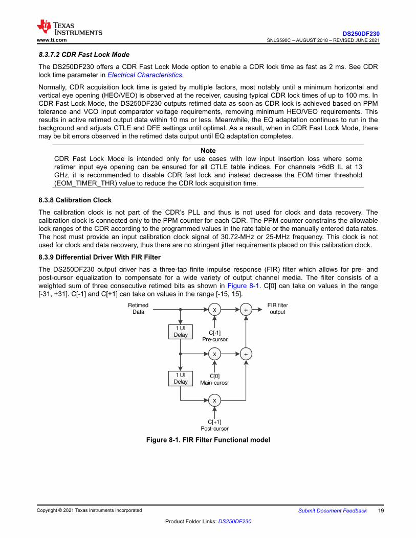
8.3.7.2 CDR Fast Lock Mode
The DS250DF230 offers a CDR Fast Lock Mode option to enable a CDR lock time as fast as 2 ms. See CDR lock time parameter in Electrical Characteristics.
Normally, CDR acquisition lock time is gated by multiple factors, most notably until a minimum horizontal and vertical eye opening (HEO/VEO) is observed at the receiver, causing typical CDR lock times of up to 100 ms. In CDR Fast Lock Mode, the DS250DF230 outputs retimed data as soon as CDR lock is achieved based on PPM tolerance and VCO input comparator voltage requirements, removing minimum HEO/VEO requirements. This results in active retimed output data within 10 ms or less. Meanwhile, the EQ adaptation continues to run in the background and adjusts CTLE and DFE settings until optimal. As a result, when in CDR Fast Lock Mode, there may be bit errors observed in the retimed data output until EQ adaptation completes.
NoteCDR Fast Lock Mode is intended only for use cases with low input insertion loss where some retimer input eye opening can be ensured for all CTLE table indices. For channels >6dB IL at 13 GHz, it is recommended to disable CDR fast lock and instead decrease the EOM timer threshold (EOM_TIMER_THR) value to reduce the CDR lock acquisition time.
8.3.8 Calibration Clock
The calibration clock is not part of the CDR’s PLL and thus is not used for clock and data recovery. The calibration clock is connected only to the PPM counter for each CDR. The PPM counter constrains the allowable lock ranges of the CDR according to the programmed values in the rate table or the manually entered data rates. The host must provide an input calibration clock signal of 30.72-MHz or 25-MHz frequency. This clock is not used for clock and data recovery, thus there are no stringent jitter requirements placed on this calibration clock.
8.3.9 Differential Driver With FIR Filter
The DS250DF230 output driver has a three-tap finite impulse response (FIR) filter which allows for pre- and post-cursor equalization to compensate for a wide variety of output channel media. The filter consists of a weighted sum of three consecutive retimed bits as shown in Figure 8-1. C[0] can take on values in the range [-31, +31]. C[-1] and C[+1] can take on values in the range [-15, 15].
x
1 UI Delay
1 UI Delay
x
x
C[-1]Pre-cursor
C[0]Main-curosr
C[+1]Post-cursor
+
+
Retimed Data
FIR filter output
Figure 8-1. FIR Filter Functional model
www.ti.comDS250DF230
SNLS590C – AUGUST 2018 – REVISED JUNE 2021
Copyright © 2021 Texas Instruments Incorporated Submit Document Feedback 19
Product Folder Links: DS250DF230

When using the FIR filter, it is important to abide by these general rules:
• |C[-1]| + |C[0]| + |C[+1]| ≤ 31; the FIR tap coefficients absolute sum must be less or equal to 31• sgn(C[-1]) = sgn(C[+1]) ≠ sgn(C[0]), for high-pass filter effect; the sign for the pre-cursor and/or post-cursor
tap must be different from main-cursor tap to realize boost effect• sgn(C[-1]) = sgn(C[+1]) = sgn(C[0]), for low-pass filter effect; the sign for the pre-cursor and/or post-cursor tap
must be equal to the main-cursor tap to realize attenuation effect
The FIR filter is used to pre-distort the transmitted waveform to compensate for frequency-dependant loss in the output channel. The most common way of pre-distorting the signal is to accentuate the transitions and de-emphasize the non-transitions. The bit before a transition is accentuated through the pre-cursor tap, and the bit after the transition is accentuated through the post-cursor tap. The waveforms in Figure 8-2 through Figure 8-4 give a conceptual illustration of how the FIR filter affects the output waveform. These characteristics can be derived from the example waveforms:
• VODpk-pk= v7 – v8• VODlow-frequency = v2 – v5• RpredB = 20 × log10 (v3 ⁄v2 )• RpstdB = 20 × log10 (v1 ⁄v2 )
Differential
Voltage
Time [UI]
v1
v2 v3
v4
v5 v6
v7
v8
0V
Transmitted
Bits: 0 0 1 1 1 1 0 0 0 0 1 0 1
Figure 8-2. Conceptual FIR Waveform With Post-Cursor Only
Differential
Voltage
Time [UI]
v1 v2
v3
v4 v5
v6
v7
v8
0V
Transmitted
Bits: 0 0 1 1 1 1 0 0 0 0 1 0 1
Figure 8-3. Conceptual FIR Waveform With Pre-Cursor Only
DS250DF230SNLS590C – AUGUST 2018 – REVISED JUNE 2021 www.ti.com
20 Submit Document Feedback Copyright © 2021 Texas Instruments Incorporated
Product Folder Links: DS250DF230

Differential
Voltage
Time [UI]
v1
v2
v3
v4
v5
v6
v7
v8
0V
Transmitted
Bits: 0 0 1 1 1 1 0 0 0 0 1 0 1
Figure 8-4. Conceptual FIR Waveform With Both Pre- and Post-Cursor
8.3.9.1 Setting the Output VOD, Pre-Cursor, and Post-Cursor Equalization
The output differential voltage (VOD), pre-cursor, and post-cursor equalization of the driver is controlled by manipulating the FIR tap settings. The main cursor tap is the primary knob for amplitude adjustment. The pre- and post-cursor FIR tap settings can then be adjusted to provide equalization. To maintain a constant peak-to-peak VOD, the user must adjust the main cursor tap value relative to the pre- and post-cursor tap changes so as to maintain a constant absolute sum of the FIR tap values. Table 8-2 shows various settings for VOD settings ranging from 350 mVpp to 1195 mVpp (typical). Note that the output peak-to-peak amplitude is a function of the sum of the absolute values of the taps, whereas the low-frequency amplitude is purely a function of the main-cursor value.
Table 8-2. Typical VOD and FIR ValuesFIR SETTINGS
Peak-to Peak VOD(V) RPRE(dB) RPST(dB)PRE-CURSOR:
REG_0x3E[6:0]MAIN-CURSOR:REG_0x3D[6:0]
POST-CURSOR:REG_0x3F[6:0]
0 +3 0 0.350 NA NA
0 +4 0 0.392 NA NA
0 +5 0 0.436 NA NA
0 +6 0 0.482 NA NA
0 +7 0 0.524 NA NA
0 +8 0 0.562 NA NA
0 +9 0 0.602 NA NA
0 +10 0 0.638 NA NA
0 +11 0 0.678 NA NA
0 +12 0 0.710 NA NA
0 +13 0 0.748 NA NA
0 +14 0 0.782 NA NA
0 +15 0 0.816 NA NA
0 +16 0 0.846 NA NA
0 +17 0 0.880 NA NA
0 +18 0 0.910 NA NA
0 +19 0 0.944 NA NA
0 +20 0 0.968 NA NA
0 +21 0 0.998 NA NA
0 +22 0 1.028 NA NA
www.ti.comDS250DF230
SNLS590C – AUGUST 2018 – REVISED JUNE 2021
Copyright © 2021 Texas Instruments Incorporated Submit Document Feedback 21
Product Folder Links: DS250DF230
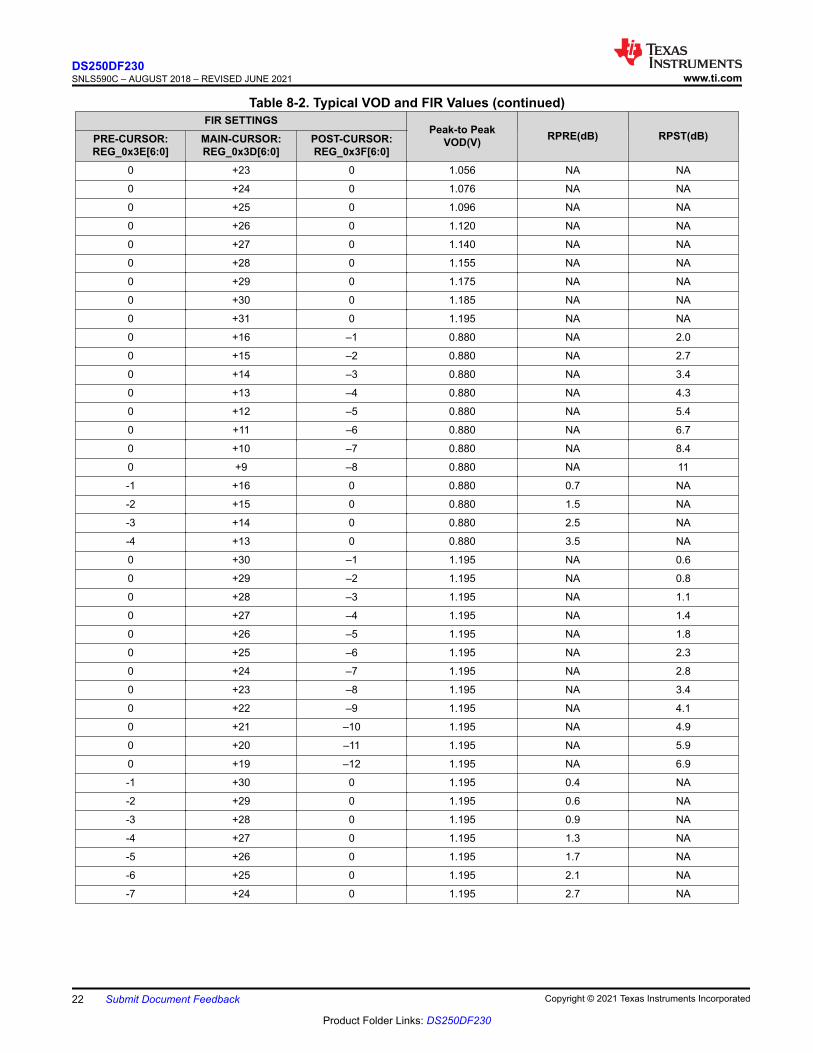
Table 8-2. Typical VOD and FIR Values (continued)FIR SETTINGS
Peak-to Peak VOD(V) RPRE(dB) RPST(dB)PRE-CURSOR:
REG_0x3E[6:0]MAIN-CURSOR:REG_0x3D[6:0]
POST-CURSOR:REG_0x3F[6:0]
0 +23 0 1.056 NA NA
0 +24 0 1.076 NA NA
0 +25 0 1.096 NA NA
0 +26 0 1.120 NA NA
0 +27 0 1.140 NA NA
0 +28 0 1.155 NA NA
0 +29 0 1.175 NA NA
0 +30 0 1.185 NA NA
0 +31 0 1.195 NA NA
0 +16 –1 0.880 NA 2.0
0 +15 –2 0.880 NA 2.7
0 +14 –3 0.880 NA 3.4
0 +13 –4 0.880 NA 4.3
0 +12 –5 0.880 NA 5.4
0 +11 –6 0.880 NA 6.7
0 +10 –7 0.880 NA 8.4
0 +9 –8 0.880 NA 11
-1 +16 0 0.880 0.7 NA
-2 +15 0 0.880 1.5 NA
-3 +14 0 0.880 2.5 NA
-4 +13 0 0.880 3.5 NA
0 +30 –1 1.195 NA 0.6
0 +29 –2 1.195 NA 0.8
0 +28 –3 1.195 NA 1.1
0 +27 –4 1.195 NA 1.4
0 +26 –5 1.195 NA 1.8
0 +25 –6 1.195 NA 2.3
0 +24 –7 1.195 NA 2.8
0 +23 –8 1.195 NA 3.4
0 +22 –9 1.195 NA 4.1
0 +21 –10 1.195 NA 4.9
0 +20 –11 1.195 NA 5.9
0 +19 –12 1.195 NA 6.9
-1 +30 0 1.195 0.4 NA
-2 +29 0 1.195 0.6 NA
-3 +28 0 1.195 0.9 NA
-4 +27 0 1.195 1.3 NA
-5 +26 0 1.195 1.7 NA
-6 +25 0 1.195 2.1 NA
-7 +24 0 1.195 2.7 NA
DS250DF230SNLS590C – AUGUST 2018 – REVISED JUNE 2021 www.ti.com
22 Submit Document Feedback Copyright © 2021 Texas Instruments Incorporated
Product Folder Links: DS250DF230

The recommended pre-cursor and post-cursor settings for a given channel will depend on the channel characteristics (mainly insertion loss) as well as the equalization capabilities of the downstream receiver. The DS250DF230 receiver, with its highly-capable CTLE and DFE, does not require a significant amount of pre- or post-cursor. The guidelines in Figure 8-5 through Figure 8-7 give general recommendations for pre- and post-cursor for different channel loss conditions. The insertion loss (IL) in these plots refers to the total loss between the link partner transmitter and the DS250DF230 receiver.
Figure 8-5. Guideline for Link Partner FIR Settings When IL ≤ 15 dB
www.ti.comDS250DF230
SNLS590C – AUGUST 2018 – REVISED JUNE 2021
Copyright © 2021 Texas Instruments Incorporated Submit Document Feedback 23
Product Folder Links: DS250DF230

Figure 8-6. Guideline for Link Partner FIR Settings When IL ≤ 25 dB
Figure 8-7. Guideline for Link Partner FIR Settings When IL ≤ 35 dB
DS250DF230SNLS590C – AUGUST 2018 – REVISED JUNE 2021 www.ti.com
24 Submit Document Feedback Copyright © 2021 Texas Instruments Incorporated
Product Folder Links: DS250DF230

8.3.9.2 Output Driver Polarity Inversion
In some applications, it may be necessary to invert the polarity of the data transmitted from the retimer. To invert the polarity of the data, read back the FIR polarity settings for the pre-, main and post-cursor taps and then invert these bits.
8.3.9.3 Slow Slew Rate
In some low speed applications, it may be needed to adjust the slew rate of the data transmitted from the retimer. DS250DF230 does offer this option. See output transition-time parameter from Electrical Characteristics. It is not recommended to use the slow rate setting for divide-by-1 data rate applications.
8.3.10 Debug Features8.3.10.1 Pattern Generator
Each channel in the DS250DF230 can be configured to generate a 16-bit user-defined data pattern or a pseudo-random bit sequence (PRBS). The user defined pattern can also be set to automatically invert every other 16-bit symbol for DC balancing purposes. The DS250DF230 pattern generator supports the following PRBS sequences:
• PRBS – 27 – 1• PRBS – 29 – 1• PRBS – 211 – 1• PRBS – 215 – 1• PRBS – 223 – 1• PRBS – 231 – 1
8.3.10.2 Pattern Checker
The pattern checker can be manually set to look for specific PRBS sequences and polarities or it can be set to automatically detect the incoming pattern and polarity. The PRBS checker supports the same set of PRBS patterns as the PRBS generator.
The pattern checker consists of an 11-bit error counter. The pattern checker uses 32-bit words, but every bit in the word is checked for error, so the error count represents the count of single bit errors.
To read out the bit and error counters, the pattern checker must first be frozen. Continuous operation with simultaneous read out of the bit and error counters is not supported in this implementation. Once the bit and error counter is read, they can be unfrozen to continue counting.
8.3.10.3 Eye-Opening Monitor
The DS250DF230’s Eye-Opening Monitor (EOM) measures the internal data eye at the input of the decision slicer and can be used for 2 functions:
1. Horizontal Eye Opening (HEO) and Vertical Eye Opening (VEO) measurement2. Full Eye Diagram Capture
The HEO measurement is made at the 0 V crossing and is read in channel register 0x27. The VEO measurement is made at the 0.5 UI mark and is read in channel register 0x28. The HEO and VEO registers can be read from channel registers 0x27 and 0x28 at any time while the CDR is locked. The following equations are used to convert the contents of channel registers 0x27 and 0x28 into their appropriate units:
• HEO [UI] = Reg_0x27 ÷ 32• VEO [mV] = Reg_0x28 × 3.125
A full eye diagram capture can be performed when the CDR is locked. The eye diagram is constructed within a 64 × 64 array, where each cell in the matrix consists of an 16-bit word representing the total number of hits recorded at that particular phase and voltage offset. Users can manually adjust the vertical scaling of the EOM or allow the state machine to control the scaling which is the default option. The horizontal scaling controlled by the state machine is always directly proportional to the data rate.
www.ti.comDS250DF230
SNLS590C – AUGUST 2018 – REVISED JUNE 2021
Copyright © 2021 Texas Instruments Incorporated Submit Document Feedback 25
Product Folder Links: DS250DF230

When a full eye diagram plot is captured, the retimer will shift out four 16-bit words of residual data that must be discarded followed by 4096 16-bit words that make up the 64 × 64 eye plot. The first actual word of the eye plot from the retimer is for (X, Y) position (0,0), which is the earliest position in time and the most negative position in voltage. Each time the eye plot data is read out, the voltage position is incremented. Once the voltage position has incremented to position 63 (the most positive voltage), the next read will cause the voltage position to reset to 0 (the most negative voltage) and the phase position to increment. This process will continue until the entire 64 × 64 matrix is read out. Figure 8-8 shows the EOM read out sequence overlaid on top of a simple eye opening plot. In this plot any hits are shown in green. This type of plot is helpful for quickly visualizing the HEO and VEO. Users can apply different algorithms to the output data to plot density or color gradients to the output data.
63
63
63
0 64
127
4032
4095
Phase Position
Voltag
e P
ositio
n
Figure 8-8. EOM Full Eye Capture Readout
To manually control the EOM vertical range, remove scaling control from the state machine then select the desired range:
Channel Reg 0x2C[6] → 0 (see Table 8-3).
Table 8-3. Eye-Opening Monitor Vertical Range SettingsCH REG 0x11[7:6] VALUE EOM VERTICAL RANGE [mV]
2’b00 ±100
2'b01 ±200
2'b10 ±300
2'b11 ±400
The EOM operates as an under-sampled circuit. This allows the EOM to be useful in identifying over equalization, ringing and other gross signal conditioning issues. However, the EOM cannot be correlated to a bit error rate.
The EOM can be accessed in two ways to read out the entire eye plot:
• Multi-byte reads can be used such that data is repeatedly latched out from channel register 0x25.• With single byte reads, the MSB are located in register 0x25 and the LSB are located in register 0x26. In this
mode, the device must be addressed each time a new byte is read.
To perform a full eye capture with the EOM, follow the steps listed in Table 8-4 within the desired channel register set:
DS250DF230SNLS590C – AUGUST 2018 – REVISED JUNE 2021 www.ti.com
26 Submit Document Feedback Copyright © 2021 Texas Instruments Incorporated
Product Folder Links: DS250DF230

Table 8-4. Eye-Opening Monitor Full Eye Capture InstructionsSTEP REGISTER [bits] Operation VALUE DESCRIPTION
1 0x67[5] Write 0 Disable lock EOM lock monitoring
20x2C[6] Write 0
Set the desired EOM vertical range0x11[7:6] Write 2'b--
3 0x11[5] Write 0 Power on the EOM
4 0x24[7] Write 1 Enable fast EOM
50x24[0]0x250x26
Read 1
Begin read out of the 64 × 64 array, discard first 4 wordsCh reg 0x24[0] is self-clearing.
0x25 is the MSB of the 16-bit word
0x26 is the LSB of the 16-bit word
60x25
Read Continue reading information until the 64 × 64 array is complete.0x26
7
0x67[5] Write 1
Return the EOM to its original state. Undo steps 1-40x2C[6] Write 1
0x11[5] Write 1
0x24[7] Write 0
8.3.11 Interrupt Signals
The DS250DF230 can be configured to report different events as interrupt signals. These interrupt signals do not impact the operation of the device, but merely report that the selected event has occurred. The interrupt bits in the register sets are all sticky bits. This means that when an event triggers an interrupt the status bit for that interrupt is set to logic HIGH. This interrupt status bit will remain at logic HIGH until the bit has been read. Once the bit has been read it will be automatically cleared, which allows for new interrupts to be detected. The DS250DF230 will report the occurrence of an interrupt through the INT_N pin. The INT_N pin is an open-drain output that will pull the line low when an interrupt signal is triggered.
Note that all available interrupts are disabled by default. Users must activate the various interrupts before they can be used.
The interrupts available in the DS250DF230 are:• CDR loss of lock• CDR locked• Signal detect loss• Signal detected• PRBS pattern checker bit error detected• HEO/VEO threshold violation
When an interrupt occurs, share register 0x08 reports which channel generated the interrupt request. Users can then select one or more of the channels that generated the interrupt request and service the interrupt by reading the appropriate interrupt status bits in the corresponding channel registers. For more information on reading interrupt status, refer to the DS2x0DF810, DS250DFx10, DS250DF230 Programmer's Guide.
www.ti.comDS250DF230
SNLS590C – AUGUST 2018 – REVISED JUNE 2021
Copyright © 2021 Texas Instruments Incorporated Submit Document Feedback 27
Product Folder Links: DS250DF230
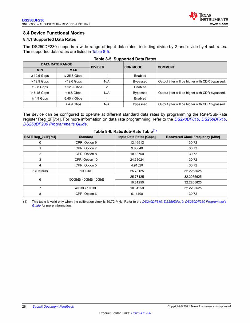
8.4 Device Functional Modes8.4.1 Supported Data Rates
The DS250DF230 supports a wide range of input data rates, including divide-by-2 and divide-by-4 sub-rates. The supported data rates are listed in Table 8-5.
Table 8-5. Supported Data RatesDATA RATE RANGE
DIVIDER CDR MODE COMMENTMIN MAX
≥ 19.6 Gbps ≤ 25.8 Gbps 1 Enabled
> 12.9 Gbps <19.6 Gbps N/A Bypassed Output jitter will be higher with CDR bypassed.
≥ 9.8 Gbps ≤ 12.9 Gbps 2 Enabled
> 6.45 Gbps < 9.8 Gbps N/A Bypassed Output jitter will be higher with CDR bypassed.
≥ 4.9 Gbps 6.45 ≤ Gbps 4 Enabled
< 4.9 Gbps N/A Bypassed Output jitter will be higher with CDR bypassed.
The device can be configured to operate at different standard data rates by programming the Rate/Sub-Rate register Reg_2F[7:4], For more information on data rate programming, refer to the DS2x0DF810, DS250DFx10, DS250DF230 Programmer's Guide.
Table 8-6. Rate/Sub-Rate Table(1)
RATE Reg_0x2F[7:4] Standard Input Data Rates [Gbps] Recovered Clock Frequency [MHz]0 CPRI Option 9 12.16512 30.72
1 CPRI Option 7 9.83040 30.72
2 CPRI Option 8 10.13760 30.72
3 CPRI Option 10 24.33024 30.72
4 CPRI Option 5 4.91520 30.72
5 (Default) 100GbE 25.78125 32.2265625
6 100GbE/ 40GbE/ 10GbE25.78125 32.2265625
10.31250 32.2265625
7 40GbE/ 10GbE 10.31250 32.2265625
8 CPRI Option 6 6.14400 30.72
(1) This table is valid only when the calibration clock is 30.72-MHz. Refer to the DS2x0DF810, DS250DFx10, DS250DF230 Programmer's Guide for more information.
DS250DF230SNLS590C – AUGUST 2018 – REVISED JUNE 2021 www.ti.com
28 Submit Document Feedback Copyright © 2021 Texas Instruments Incorporated
Product Folder Links: DS250DF230

8.4.2 SMBus Master Mode
SMBus master mode allows the DS250DF230 to program itself by reading directly from an external EEPROM. When using the SMBus master mode, the DS250DF230 will read directly from specific location in the external EEPROM. When designing a system for using the external EEPROM, the user must follow these specific guidelines:• Maximum EEPROM size is 2048 Bytes• Minimum EEPROM size for a single DS250DF230 with individual channel configuration is 161 Bytes (3 base
header bytes + 12 address map bytes + 2 × 72 channel register bytes + 2 share register bytes; bytes are defined to be 8-bits)
• Set ENSMB = Float, for SMBus master mode• The external EEPROM device address byte must be 0xA0• The external EEPROM device must support 400kHz operation at 2.5-V or 3.3-V supply• THR pin is pulled low by 1 kΩ to GND, so that DS250DF230 is working under 2.5-V/3.3-V SMBus interface
mode• Set the SMBus address of the DS250DF230 by configuring the ADDR0 and ADDR1 pins
When loading multiple DS250DF230 devices from the same EEPROM, use these guidelines to configure the devices:• Configure the SMBus addresses for each DS250DF230 to be sequential. The first device in the sequence
must have an address of 0x30• Daisy chain READ_EN_N and ALL_DONE_N from one device to the next device in the sequence so that
they do not compete for the EEPROM at the same time.• If all of the DS250DF230 devices share the same EEPROM channel and share register settings, configure
the common channel bit in the base header to 1. With common channel configuration enabled, each DS250DF230 device will configure all 2 channels with the same settings.
When loading a single DS250DF230 from an EEPROM, use these guidelines to configure the device:• Set the common channel bit to 0 to allow for individual channel configuration, or set the common channel bit
to 1 to load the same configuration settings to all channels.• When configuring individual channels, a 512, 1024 or 2048 Byte EEPROM must be used.• If there are more than three DS250DF230 devices on a PCB that require individual channel configuration,
then each device must have its own EEPROM.
www.ti.comDS250DF230
SNLS590C – AUGUST 2018 – REVISED JUNE 2021
Copyright © 2021 Texas Instruments Incorporated Submit Document Feedback 29
Product Folder Links: DS250DF230
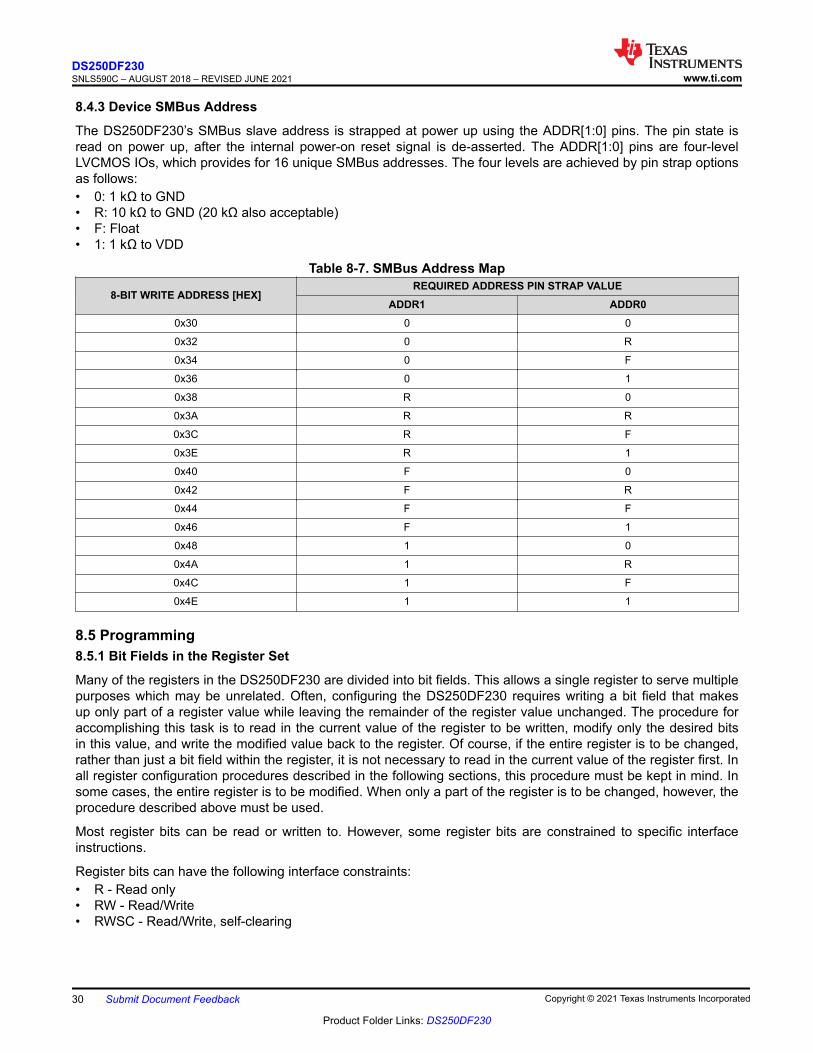
8.4.3 Device SMBus Address
The DS250DF230’s SMBus slave address is strapped at power up using the ADDR[1:0] pins. The pin state is read on power up, after the internal power-on reset signal is de-asserted. The ADDR[1:0] pins are four-level LVCMOS IOs, which provides for 16 unique SMBus addresses. The four levels are achieved by pin strap options as follows:• 0: 1 kΩ to GND• R: 10 kΩ to GND (20 kΩ also acceptable)• F: Float• 1: 1 kΩ to VDD
Table 8-7. SMBus Address Map
8-BIT WRITE ADDRESS [HEX]REQUIRED ADDRESS PIN STRAP VALUE
ADDR1 ADDR00x30 0 0
0x32 0 R
0x34 0 F
0x36 0 1
0x38 R 0
0x3A R R
0x3C R F
0x3E R 1
0x40 F 0
0x42 F R
0x44 F F
0x46 F 1
0x48 1 0
0x4A 1 R
0x4C 1 F
0x4E 1 1
8.5 Programming8.5.1 Bit Fields in the Register Set
Many of the registers in the DS250DF230 are divided into bit fields. This allows a single register to serve multiple purposes which may be unrelated. Often, configuring the DS250DF230 requires writing a bit field that makes up only part of a register value while leaving the remainder of the register value unchanged. The procedure for accomplishing this task is to read in the current value of the register to be written, modify only the desired bits in this value, and write the modified value back to the register. Of course, if the entire register is to be changed, rather than just a bit field within the register, it is not necessary to read in the current value of the register first. In all register configuration procedures described in the following sections, this procedure must be kept in mind. In some cases, the entire register is to be modified. When only a part of the register is to be changed, however, the procedure described above must be used.
Most register bits can be read or written to. However, some register bits are constrained to specific interface instructions.
Register bits can have the following interface constraints:• R - Read only• RW - Read/Write• RWSC - Read/Write, self-clearing
DS250DF230SNLS590C – AUGUST 2018 – REVISED JUNE 2021 www.ti.com
30 Submit Document Feedback Copyright © 2021 Texas Instruments Incorporated
Product Folder Links: DS250DF230

8.5.2 Writing to and Reading from the Global/Shared/Channel Registers
The DS250DF230 has 3 types of registers:1. Global Registers – These registers can be accessed at any time and are used to select individual channel
registers, the shared registers or to read back the TI ID and version information.2. Shared Registers – These registers are used for device-level configuration, status read back or control.3. Channel Registers – These registers are used to control and configure specific features for each individual
channel. All channels have the same channel register set and can be configured independent of each other.
The global registers can be accessed at any time, regardless of whether the shared or channel register set is selected. The DS250DF230 global registers are located on addresses 0xEF-0xFF. The function of the global registers falls into the following categories:• Channel selection and share enabling – Registers 0xFC and 0xFF• Device and version information – Registers 0xEF-0xF3• Reserved/unused registers – all other addresses
Register 0xFC is used to select the channel registers to be written to. To select a channel, write a 1 to its corresponding bit in register 0xFC. Note that more than one channel may be written to by setting multiple bits in register 0xFC. However, when performing an SMBus read transaction only one channel can be selected at a time. If multiple channels are selected in register 0xFC when attempting to perform an SMBus read, the device will return 0xFF.
Register 0xFF bit 1 can be used to perform broadcast register writes to all channels. A single channel read-modify broadcast write type commands can be accomplished by setting register 0xFF to 0x03 and selecting a single channel in register 0xFC. This type of configuration allows for the reading of a single channel's register information and then writing to all channels with the modified value. Register 0xFF bit 0 is used to select the shared register page or the channel register page for the channels selected in register 0xFC.
TI repeaters/retimers have a vendor ID register (0xFE) which will always read back 0x03. In addition, there are three device ID registers (0xF0, 0xF1, and 0xF3). These are useful to verify that there is a good SMBus connection between the SMBus master and the DS250DF230.
www.ti.comDS250DF230
SNLS590C – AUGUST 2018 – REVISED JUNE 2021
Copyright © 2021 Texas Instruments Incorporated Submit Document Feedback 31
Product Folder Links: DS250DF230
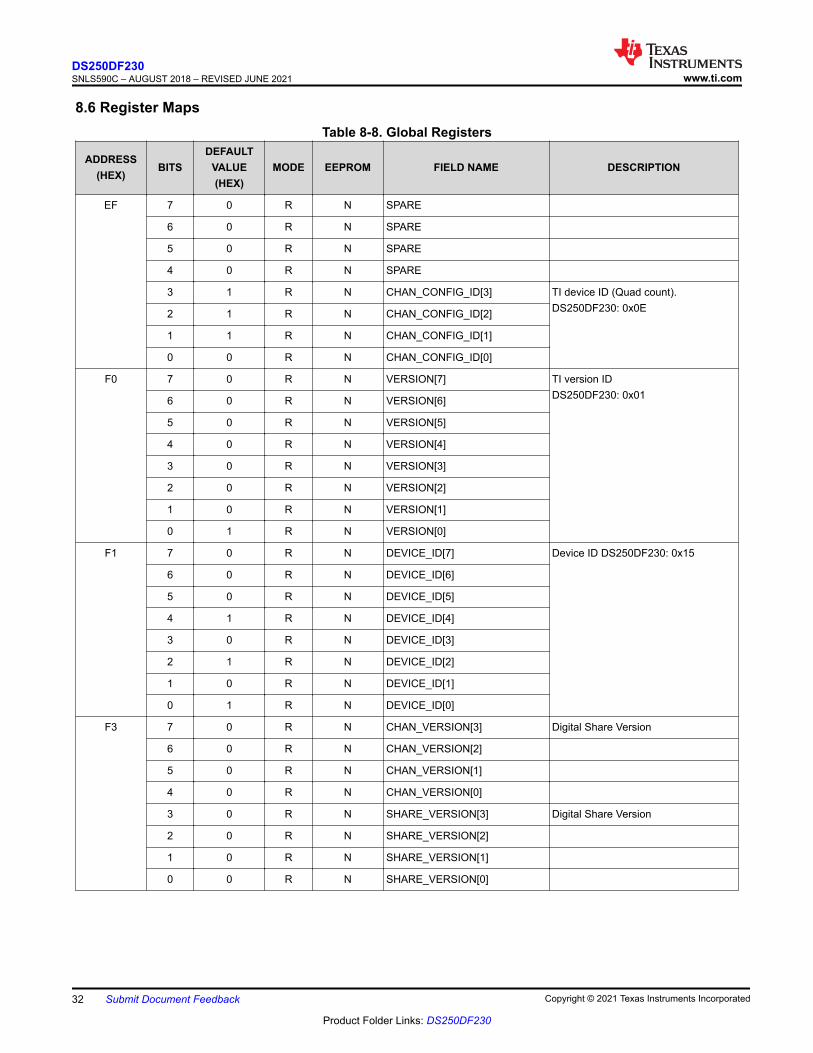
8.6 Register MapsTable 8-8. Global Registers
ADDRESS(HEX)
BITSDEFAULT
VALUE(HEX)
MODE EEPROM FIELD NAME DESCRIPTION
EF 7 0 R N SPARE
6 0 R N SPARE
5 0 R N SPARE
4 0 R N SPARE
3 1 R N CHAN_CONFIG_ID[3] TI device ID (Quad count).DS250DF230: 0x0E2 1 R N CHAN_CONFIG_ID[2]
1 1 R N CHAN_CONFIG_ID[1]
0 0 R N CHAN_CONFIG_ID[0]
F0 7 0 R N VERSION[7] TI version IDDS250DF230: 0x016 0 R N VERSION[6]
5 0 R N VERSION[5]
4 0 R N VERSION[4]
3 0 R N VERSION[3]
2 0 R N VERSION[2]
1 0 R N VERSION[1]
0 1 R N VERSION[0]
F1 7 0 R N DEVICE_ID[7] Device ID DS250DF230: 0x15
6 0 R N DEVICE_ID[6]
5 0 R N DEVICE_ID[5]
4 1 R N DEVICE_ID[4]
3 0 R N DEVICE_ID[3]
2 1 R N DEVICE_ID[2]
1 0 R N DEVICE_ID[1]
0 1 R N DEVICE_ID[0]
F3 7 0 R N CHAN_VERSION[3] Digital Share Version
6 0 R N CHAN_VERSION[2]
5 0 R N CHAN_VERSION[1]
4 0 R N CHAN_VERSION[0]
3 0 R N SHARE_VERSION[3] Digital Share Version
2 0 R N SHARE_VERSION[2]
1 0 R N SHARE_VERSION[1]
0 0 R N SHARE_VERSION[0]
DS250DF230SNLS590C – AUGUST 2018 – REVISED JUNE 2021 www.ti.com
32 Submit Document Feedback Copyright © 2021 Texas Instruments Incorporated
Product Folder Links: DS250DF230

Table 8-8. Global Registers (continued)
ADDRESS(HEX)
BITSDEFAULT
VALUE(HEX)
MODE EEPROM FIELD NAME DESCRIPTION
FB 7 0 RW N RESERVED RESERVED
6 0 RW N RESERVED RESERVED
5 0 RW N RESERVED RESERVED
4 0 RW N RESERVED RESERVED
3 0 RW N RESERVED RESERVED
2 1 RW N RESERVED RESERVED
1 0 RW N RESERVED RESERVED
0 0 RW N RESERVED RESERVED
FC 7 0 RW N EN_CH7
6 0 RW N EN_CH6
5 0 RW N EN_CH5
4 0 RW N EN_CH4
3 0 RW N EN_CH3
2 0 RW N EN_CH2
1 0 RW N EN_CH1 Select channel 1
0 0 RW N EN_CH0 Select channel 0
FD 7 0 RW N RESERVED RESERVED
6 0 RW N RESERVED RESERVED
5 0 RW N RESERVED RESERVED
4 0 RW N RESERVED RESERVED
3 0 RW N RESERVED RESERVED
2 0 RW N RESERVED RESERVED
1 0 RW N RESERVED RESERVED
0 0 RW N RESERVED RESERVED
FE 7 0 R N VENDOR_ID[7] TI vendor ID
6 0 R N VENDOR_ID[6]
5 0 R N VENDOR_ID[5]
4 0 R N VENDOR_ID[4]
3 0 R N VENDOR_ID[3]
2 0 R N VENDOR_ID[2]
1 1 R N VENDOR_ID[1]
0 1 R N VENDOR_ID[0]
www.ti.comDS250DF230
SNLS590C – AUGUST 2018 – REVISED JUNE 2021
Copyright © 2021 Texas Instruments Incorporated Submit Document Feedback 33
Product Folder Links: DS250DF230

Table 8-8. Global Registers (continued)
ADDRESS(HEX)
BITSDEFAULT
VALUE(HEX)
MODE EEPROM FIELD NAME DESCRIPTION
FF 7 0 RW N RESERVED RESERVED
6 0 RW N RESERVED RESERVED
5 0 RW NEN_SHARE_Q1 Select shared registers for quad 1
(DS250DF810, DS280DF810 only)DS250DF230: 0
4 0 RW N EN_SHARE_Q0 Select shared registers for quad 0
3 0 RW N RESERVED RESERVED
2 0 RW N RESERVED RESERVED
1 0 RW N
WRITE_ALL_CH Allows user to write to all channels as if they are the same, but only allows read back from the channel specified in 0xFC.Note: EN_CH_SMB must be = 1 or else this function is invalid.
0 0 RW NEN_CH_SMB 1: Enables SMBUS access to the
channels specified in Reg_0xFC0: The shared registers are selected
DS250DF230SNLS590C – AUGUST 2018 – REVISED JUNE 2021 www.ti.com
34 Submit Document Feedback Copyright © 2021 Texas Instruments Incorporated
Product Folder Links: DS250DF230

Table 8-9. Shared Registers
ADDRESS(HEX)
BITSDEFAULT
VALUE(HEX)
MODE EEPROMFIELDNAME
DESCRIPTION
00 7 0 R N SMBUS_ADDR[3] SMBus AddressStrapped 7-bit address is 0x18 + SMBus_Addr[3:0]
6 0 R N SMBUS_ADDR[2]
5 0 R N SMBUS_ADDR[1]
4 0 R N SMBUS_ADDR[0]
3:0 0 R N RESERVED RESERVED
01 7 0 R N RESERVED RESERVED
6 0 R N RESERVED RESERVED
5 0 R N RESERVED RESERVED
4 1 R N RESERVED RESERVED
3 0 R N RESERVED RESERVED
2 1 R N RESERVED RESERVED
1 0 R N RESERVED RESERVED
0 1 R N RESERVED RESERVED
02 7:0 0 RW N RESERVED RESERVED
03 7:0 0 RW N RESERVED RESERVED
04 7 0 RW N RESERVED RESERVED
6 0 RWSC NRST_I2C_REGS 1: Reset shared registers. This bit is
self-clearing.0: Normal operation
5 0 RWSC NRST_I2C_MAS 1: Reset for SMBus/I2C Master. This
bit is self-clearing.0: Normal operation
4 0 RW NFRC_EEPRM_RD 1: Force EEPROM Configuration
0: Normal operation
3 1 RW Y RESERVED RESERVED
2 0 RW N RESERVED RESERVED
1 0 RW N RESERVED RESERVED
0 1 RW N RESERVED RESERVED
www.ti.comDS250DF230
SNLS590C – AUGUST 2018 – REVISED JUNE 2021
Copyright © 2021 Texas Instruments Incorporated Submit Document Feedback 35
Product Folder Links: DS250DF230
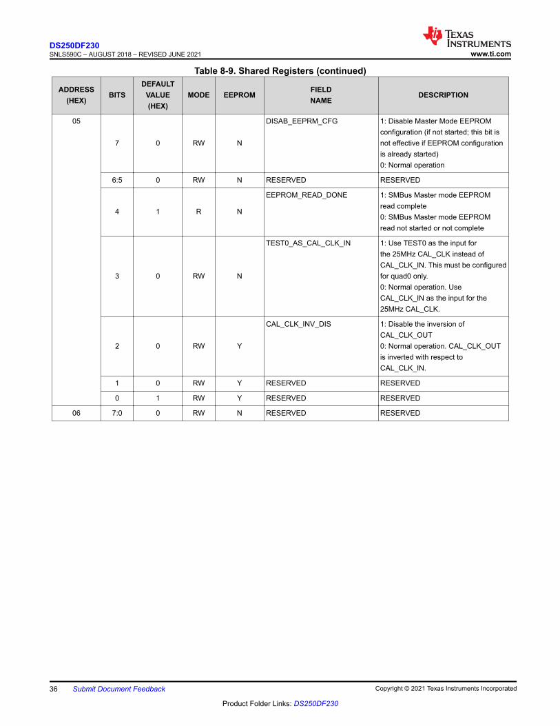
Table 8-9. Shared Registers (continued)
ADDRESS(HEX)
BITSDEFAULT
VALUE(HEX)
MODE EEPROMFIELDNAME
DESCRIPTION
05
7 0 RW N
DISAB_EEPRM_CFG 1: Disable Master Mode EEPROM configuration (if not started; this bit is not effective if EEPROM configuration is already started)0: Normal operation
6:5 0 RW N RESERVED RESERVED
4 1 R N
EEPROM_READ_DONE 1: SMBus Master mode EEPROM read complete0: SMBus Master mode EEPROM read not started or not complete
3 0 RW N
TEST0_AS_CAL_CLK_IN 1: Use TEST0 as the input for the 25MHz CAL_CLK instead of CAL_CLK_IN. This must be configured for quad0 only.0: Normal operation. Use CAL_CLK_IN as the input for the 25MHz CAL_CLK.
2 0 RW Y
CAL_CLK_INV_DIS 1: Disable the inversion of CAL_CLK_OUT0: Normal operation. CAL_CLK_OUT is inverted with respect to CAL_CLK_IN.
1 0 RW Y RESERVED RESERVED
0 1 RW Y RESERVED RESERVED
06 7:0 0 RW N RESERVED RESERVED
DS250DF230SNLS590C – AUGUST 2018 – REVISED JUNE 2021 www.ti.com
36 Submit Document Feedback Copyright © 2021 Texas Instruments Incorporated
Product Folder Links: DS250DF230

Table 8-9. Shared Registers (continued)
ADDRESS(HEX)
BITSDEFAULT
VALUE(HEX)
MODE EEPROMFIELDNAME
DESCRIPTION
08 7 0 R N RESERVED RESERVED
6 0 R N RESERVED RESERVED
5 0 R N RESERVED RESERVED
4 0 R N RESERVED RESERVED
3 0 R N
INT_Q0C3 Interrupt from channel 3. For DS250DF810 and DS280DF810, this applies to the quad selected by Reg_0xFF[5:4]. Not applicable to DS250DF210
2 0 R N
INT_Q0C2 Interrupt from channel 2. For DS250DF810 and DS280DF810, this applies to the quad selected by Reg_0xFF[5:4]. Not applicable to DS250DF210
1 0 R N
INT_Q0C1 Interrupt from channel 1. For DS250DF810 and DS280DF810, this applies to the quad selected by Reg_0xFF[5:4].
0 0 R N
INT_Q0C0 Interrupt from channel 0. For DS250DF810 and DS280DF810, this applies to the quad selected by Reg_0xFF[5:4].
0A 7:1 0 R Y RESERVED RESERVED
0 0 RW Y
DIS_REFCLK_OUT 1: Disable CAL_CLK_OUT (high-Z)
0: Normal operation. Enable CAL_CLK_OUT
0B 7 0 RW N RESERVED RESERVED
6 0 R NREFCLK_DET 1: 25MHz clock detected on
CAL_CLK_IN0: No clock detected on CAL_CLK_IN
5 0 RW N RESERVED RESERVED
4 1 RW NRESERVED RESERVED
DS250DF230:1Other Devices: RESERVED, 0
3 0 RW NMR_REFCLK_DET_DIS 0: CAL_CLK_IN detection and status
reporting enabled (default)1: CAL_CLK_IN detection disabled
2 0 RW N RESERVED RESERVED
1 0 RW N RESERVED RESERVED
0 0 RW N RESERVED RESERVED
0C 7:0 0 RW N RESERVED RESERVED
0D 7:0 0 R N RESERVED RESERVED
www.ti.comDS250DF230
SNLS590C – AUGUST 2018 – REVISED JUNE 2021
Copyright © 2021 Texas Instruments Incorporated Submit Document Feedback 37
Product Folder Links: DS250DF230

Table 8-9. Shared Registers (continued)
ADDRESS(HEX)
BITSDEFAULT
VALUE(HEX)
MODE EEPROMFIELDNAME
DESCRIPTION
0E 7:2 0 RW N RESERVED RESERVED
1:0 0 R N RESERVED RESERVED
0F 7:0 0 RW N RESERVED RESERVED
10 7 1 RW N RESERVED RESERVED
6 1 RW N RESERVED RESERVED
5 1 RW N RESERVED RESERVED
4 1 RW N RESERVED RESERVED
3 1 RW Y RESERVED RESERVED
2 1 RW Y RESERVED RESERVED
1 1 RW Y RESERVED RESERVED
0 1 RW Y RESERVED RESERVED
11 7 0 R N EECFG_CMPLT 11: Not valid10: EEPROM load completed successfully01: EEPROM load failed after 64 attempts00: EEPROM load in progress
6 0 R N
EECFG_FAIL
5 0 R N EECFG_ATMPT[5] Number of attempts made to load EEPROM image4 0 R N EECFG_ATMPT[4]
3 0 R N EECFG_ATMPT[3]
2 0 R N EECFG_ATMPT[2]
1 0 R N EECFG_ATMPT[1]
0 0 R N EECFG_ATMPT[0]
12
7 1 RW N
REG_I2C_FAST 1: EEPROM load uses Fast I2C Mode (400 kHz)
0: EEPROM load uses Standard I2C Mode (100 kHz)
6 0 RW N RESERVED RESERVED
5 0 RW N RESERVED RESERVED
4 1 RW N RESERVED RESERVED
3 0 RW N RESERVED RESERVED
2 0 RW N RESERVED RESERVED
1 0 RW N RESERVED RESERVED
0 1 RW N RESERVED RESERVED
DS250DF230SNLS590C – AUGUST 2018 – REVISED JUNE 2021 www.ti.com
38 Submit Document Feedback Copyright © 2021 Texas Instruments Incorporated
Product Folder Links: DS250DF230

Table 8-10. Channel Registers, 0 to 39
ADDRESS(HEX)
BITSDEFAULT
VALUE(HEX)
MODE EEPROM FIELD NAME DESCRIPTION
00 7 0 RW N RESERVED RESERVED
6 0 RW N RESERVED RESERVED
5 0 RW N RESERVED RESERVED
4 0 RW N RESERVED RESERVED
3 0 RW N RST_CORE 1: Reset the 10M core clock domain. This is the main clock domain for all the state machines0: Normal operation
2 0 RW N RST_REGS 1: Reset channel registers to power-up defaults.0: Normal operation
1 0 RW N RST_VCO 1: Resets the CDR S2P clock domain, includes PPM counter, EOM counter.0: Normal operation
0 0 RW N RST_REFCLK 1: Resets the 25MHz reference clock domain, includes PPM counter. Does not work if 25MHz clock is not present.0: Normal operation
01 7 0 R N SIGDET Raw Signal Detect observation
6 0 R N POL_INV_DET Indicates PRBS checker detected polarity inversion in the locked data sequence.
5 0 R N CDR_LOCK_LOSS_INT 1: Indicates loss of CDR lock after having acquired it. Bit clears on read. Feature must be enabled with Reg_0x31[1]
4 0 R N PRBS_SEQ_DET[3] Indicates the pattern detected on the input serial stream
0xxx: No detect1000: 7 bits PRBS sequence1001: 9 bits PRBS sequence1010: 11 bits PRBS sequence1011: 15 bits PRBS sequence1100: 23 bits PRBS sequence1101: 31 bits PRBS sequence1110: 58 bits PRBS sequence1111: 63 bits PRBS sequence
3 0 R N PRBS_SEQ_DET[2]
2 0 R N PRBS_SEQ_DET[1]
1 0 R N PRBS_SEQ_DET[0]
0 0 R N SIG_DET_LOSS_INT Loss of signal indicator, set once signal is acquired and then lost. Clears on read. Feature must be enabled with reg_31[0]
www.ti.comDS250DF230
SNLS590C – AUGUST 2018 – REVISED JUNE 2021
Copyright © 2021 Texas Instruments Incorporated Submit Document Feedback 39
Product Folder Links: DS250DF230

Table 8-10. Channel Registers, 0 to 39 (continued)
ADDRESS(HEX)
BITSDEFAULT
VALUE(HEX)
MODE EEPROM FIELD NAME DESCRIPTION
02 7 0 R N CDR_STATUS[7] CDR Status [7:0]Bit[7] = PPM Count met• 1: The data rate is within
the specified PPM tolerance (typically around ±1000 ppm unless specified otherwise in Reg 0x64).
• 0: Error: PPM tolerance exceeded.
Bit[6] = Auto Adapt Complete• 1: CTLE auto-adaption is
complete.• 0: CTLE auto-adaption in
progress.
Bit[5] = Fail Lock Check• 1: Signal quality and amplitude
level is not sufficient for lock.• 0: Signal quality and amplitude
level is sufficient for CDR lock.
Bit[4] = Lock• When asserted, indicates CDR is
locked to the incoming signal.
Bit[3] = CDR Lock• When asserted, indicates CDR
is locked to the incoming signal (same status as bit 4).
Bit[2] = ReservedBit[1] = Comp LPF High• 1: Data rate exceeds the VCO
upper limit, based on loop filter comparator voltage.
• 0: Data rate is within VCO upper limit.
Bit[0] = Comp LPF Low• 1: Data rate is below the VCO
lower limit, based on loop filter comparator voltage.
• 0: Data rate is within VCO lower limit
6 0 R N CDR_STATUS[6]
5 0 R N CDR_STATUS[5]
4 0 R N CDR_STATUS[4]
3 0 R N CDR_STATUS[3]
2 0 R N CDR_STATUS[2]
1 0 R N CDR_STATUS[1]
0 0 R N CDR_STATUS[0]
DS250DF230SNLS590C – AUGUST 2018 – REVISED JUNE 2021 www.ti.com
40 Submit Document Feedback Copyright © 2021 Texas Instruments Incorporated
Product Folder Links: DS250DF230

Table 8-10. Channel Registers, 0 to 39 (continued)
ADDRESS(HEX)
BITSDEFAULT
VALUE(HEX)
MODE EEPROM FIELD NAME DESCRIPTION
03 7 0 RW Y EQ_BST0[1] This register can be used to force an EQ boost setting if used in conjunction with channel Reg_0x2D[3].
6 0 RW Y EQ_BST0[0]
5 0 RW Y EQ_BST1[1]
4 0 RW Y EQ_BST1[0]
3 0 RW Y EQ_BST2[1]
2 0 RW Y EQ_BST2[0]
1 0 RW Y EQ_BST3[1]
0 0 RW Y EQ_BST3[0]
04 7 0 RW N RESERVED RESERVED
6 0 RW N RESERVED RESERVED
5 0 RW N RESERVED RESERVED
4 0 RW N RESERVED RESERVED
3 0 RW N RESERVED RESERVED
2 0 RW N RESERVED RESERVED
1 0 RW N RESERVED RESERVED
0 1 RW N RESERVED RESERVED
05 7 0 RW N RESERVED RESERVED
6 0 RW N RESERVED RESERVED
5 0 RW N RESERVED RESERVED
4 0 RW N RESERVED RESERVED
3 0 RW N RESERVED RESERVED
2 0 RW N RESERVED RESERVED
1 0 RW N RESERVED RESERVED
0 1 RW N RESERVED RESERVED
06 7 0 RW N RESERVED RESERVED
6 0 RW N RESERVED RESERVED
5 0 RW N RESERVED RESERVED
4 0 RW N RESERVED RESERVED
3 0 RW N RESERVED RESERVED
2 0 RW N RESERVED RESERVED
1 0 RW N RESERVED RESERVED
0 1 RW N RESERVED RESERVED
www.ti.comDS250DF230
SNLS590C – AUGUST 2018 – REVISED JUNE 2021
Copyright © 2021 Texas Instruments Incorporated Submit Document Feedback 41
Product Folder Links: DS250DF230

Table 8-10. Channel Registers, 0 to 39 (continued)
ADDRESS(HEX)
BITSDEFAULT
VALUE(HEX)
MODE EEPROM FIELD NAME DESCRIPTION
07 7 0 RW N RESERVED RESERVED
6 0 RW N RESERVED RESERVED
5 0 RW N RESERVED RESERVED
4 0 RW N RESERVED RESERVED
3 0 RW N RESERVED RESERVED
2 0 RW N RESERVED RESERVED
1 0 RW N RESERVED RESERVED
0 1 RW N RESERVED RESERVED
08 7 0 RW Y RESERVED RESERVED
6 1 RW Y RESERVED RESERVED
5 1 RW Y RESERVED RESERVED
4 1 RW Y RESERVED RESERVED
3 0 RW Y RESERVED RESERVED
2 0 RW Y RESERVED RESERVED
1 1 RW Y RESERVED RESERVED
0 1 RW Y RESERVED RESERVED
09 7 0 RW Y REG_VCO_CAP_OV Enable bit to override cap_cnt with value in Reg_0x0B[4:0]
6 0 RW Y REG_SET_CP_LVL_LPF_OV Enable bit to override lpf_dac_val with value in Reg_0x1F[4:0]
5 0 RW Y REG_BYPASS_PFD_OV 0: Normal operation.
4 0 RW Y REG_EN_FD_PD_VCO_PDIQ_OV
Enable bit to override en_fd, pd_pd, pd_vco, pd_pdiq with Reg_0x1E[0], Reg_0x1E[2], Reg_0x1C[0], Reg_0x1C[1]
3 0 RW Y REG_EN_PD_CP_OV Enable bit to override pd_fd_cp and pd_pd_cp with value in Reg_0x1B[1:0]
2 0 RW Y REG_DIVSEL_OV Enable bit to override divsel with value in Reg_0x18[6:4]
1 0 RW Y RESERVED RESERVED
0 0 RW Y RESERVED RESERVED
DS250DF230SNLS590C – AUGUST 2018 – REVISED JUNE 2021 www.ti.com
42 Submit Document Feedback Copyright © 2021 Texas Instruments Incorporated
Product Folder Links: DS250DF230

Table 8-10. Channel Registers, 0 to 39 (continued)
ADDRESS(HEX)
BITSDEFAULT
VALUE(HEX)
MODE EEPROM FIELD NAME DESCRIPTION
0A 7 0 RW Y RESERVED RESERVED
6 0 RW Y REG_EN_IDAC_PD_CP_OV_AND_REG_EN_IDAC_FD_CP_OV
Enable bit to override phase detector charge pump settings with Reg_0x1C[7:5]Enable bit to override frequency detector charge pump settings with Reg_0x1C[4:2]
5 0 RW Y REG_DAC_LPF_HIGH_PHASE_OV_AND_REG_DAC_LPF_LOW_PHASE_OV
Enable bit to loop filter comparator trip voltages with Reg_0x16[7:0]
4 0 RW Y RESERVED RESERVED
3 0 RW N REG_CDR_RESET_OV Enable CDR Reset override with Reg_0x0A[2]
2 0 RW N REG_CDR_RESET_SM CDR Reset override bit
1 0 RW N REG_CDR_LOCK_OV Enable CDR lock signal override with Reg_0x0A[0]
0 0 RW N REG_CDR_LOCK CDR lock signal override bit
0B 7 0 RW Y RESERVED RESERVED
6 1 RW Y RESERVED RESERVED
5 1 RW Y RESERVED RESERVED
4 0 RW Y RESERVED RESERVED
3 0 RW Y RESERVED RESERVED
2 0 RW Y RESERVED RESERVED
1 1 RW Y RESERVED RESERVED
0 1 RW Y RESERVED RESERVED
0C 7 0 RW N RESERVED RESERVED
6 0 RW N RESERVED RESERVED
5 0 RW N RESERVED RESERVED
4 0 RW N RESERVED RESERVED
3 0 RW N RESERVED RESERVED
2 0 RW N RESERVED RESERVED
1 0 RW N RESERVED RESERVED
0 0 RW N RESERVED RESERVED
www.ti.comDS250DF230
SNLS590C – AUGUST 2018 – REVISED JUNE 2021
Copyright © 2021 Texas Instruments Incorporated Submit Document Feedback 43
Product Folder Links: DS250DF230

Table 8-10. Channel Registers, 0 to 39 (continued)
ADDRESS(HEX)
BITSDEFAULT
VALUE(HEX)
MODE EEPROM FIELD NAME DESCRIPTION
0D 7 1 RW N DES_PD 1: De-serializer (for PRBS checker) is powered down0: De-serializer (for PRBS checker) is enabled
6 0 RW N RESERVED RESERVED
5 0 RW Y RESERVED RESERVED
4 0 RW Y RESERVED RESERVED
3 0 RW Y RESERVED RESERVED
2 0 RW Y RESERVED RESERVED
1 0 RW N RESERVED RESERVED
0 0 RW N RAW_TX_SWING DS250DF230 A1 Only:0: Low Swing(Default)1: High Swing, only when CDR is bypassed. Not Recommended when CDR is enabled
0E 7 1 RW N RESERVED RESERVED
6 0 RW N RESERVED RESERVED
5 0 RW N RESERVED RESERVED
4 1 RW N RESERVED RESERVED
3 0 RW N RESERVED RESERVED
2 0 RW N RESERVED RESERVED
1 1 RW N RESERVED RESERVED
0 1 RW N RESERVED RESERVED
0F 7 0 RW N RESERVED RESERVED
6 1 RW N RESERVED RESERVED
5 1 RW N RESERVED RESERVED
4 0 RW N RESERVED RESERVED
3 1 RW N RESERVED RESERVED
2 0 RW N RESERVED RESERVED
1 0 RW N RESERVED RESERVED
0 1 RW N RESERVED RESERVED
10 7 0 RW N RESERVED RESERVED
6 0 RW N RESERVED RESERVED
5 0 RW N RESERVED RESERVED
4 0 RW N RESERVED RESERVED
3 0 RW N RESERVED RESERVED
2 0 RW N RESERVED RESERVED
1 0 RW N RESERVED RESERVED
0 0 RW N RESERVED RESERVED
DS250DF230SNLS590C – AUGUST 2018 – REVISED JUNE 2021 www.ti.com
44 Submit Document Feedback Copyright © 2021 Texas Instruments Incorporated
Product Folder Links: DS250DF230

Table 8-10. Channel Registers, 0 to 39 (continued)
ADDRESS(HEX)
BITSDEFAULT
VALUE(HEX)
MODE EEPROM FIELD NAME DESCRIPTION
11 7 0 RW Y EOM_SEL_VRANGE[1] Manually set the EOM vertical range, used with channel Reg_0x2C[6]:00: ±100 mV01: ±200 mV10: ±300 mV11: ±400 mV
6 0 RW Y EOM_SEL_VRANGE[0]
5 1 RW Y EOM_PD 1: Normal operation. Eye opening monitor (EOM) is automatically duty-cycled.0: EOM is force-enabled
4 0 RW N RESERVED RESERVED
3 0 RW Y DFE_TAP2_POL Bit forces DFE tap 2 polarity1: Negative, boosts by the specified tap weight0: Positive, attenuates by the specified tap weight
2 0 RW Y DFE_TAP3_POL Bit forces DFE tap 3 polarity1: Negative, boosts by the specified tap weight0: Positive, attenuates by the specified tap weight
1 0 RW Y DFE_TAP4_POL Bit forces DFE tap 4 polarity1: Negative, boosts by the specified tap weight0: Positive, attenuates by the specified tap weight
0 0 RW Y DFE_TAP5_POL Bit forces DFE tap 5 polarity1: Negative, boosts by the specified tap weight0: Positive, attenuates by the specified tap weight
12 7 1 RW Y DFE_TAP1_POL Bit forces DFE tap 1 polarity1: Negative, boosts by the specified tap weight0: Positive, attenuates by the specified tap weight
6 0 RW N RESERVED RESERVED
5 0 RW Y RESERVED RESERVED
4 0 RW Y DFE_WT1[4] These bits force DFE tap 1 weight. Manual DFE operation is required for this to take effect by setting Reg_0x15[7]=1.If Reg_0x15[7]=0, the value defined here is used as the initial DFE tap 1 weight during adaptation.
3 0 RW Y DFE_WT1[3]
2 0 RW Y DFE_WT1[2]
1 1 RW Y DFE_WT1[1]
0 1 RW Y DFE_WT1[0]
www.ti.comDS250DF230
SNLS590C – AUGUST 2018 – REVISED JUNE 2021
Copyright © 2021 Texas Instruments Incorporated Submit Document Feedback 45
Product Folder Links: DS250DF230
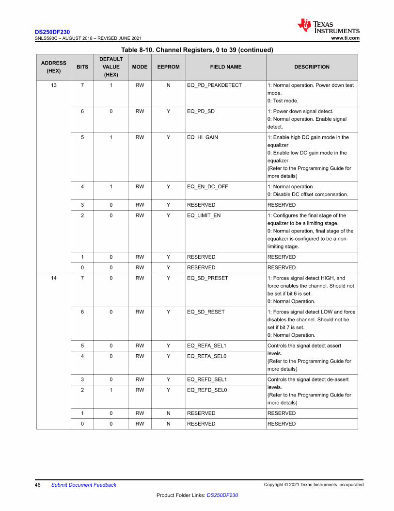
Table 8-10. Channel Registers, 0 to 39 (continued)
ADDRESS(HEX)
BITSDEFAULT
VALUE(HEX)
MODE EEPROM FIELD NAME DESCRIPTION
13 7 1 RW N EQ_PD_PEAKDETECT 1: Normal operation. Power down test mode.0: Test mode.
6 0 RW Y EQ_PD_SD 1: Power down signal detect.0: Normal operation. Enable signal detect.
5 1 RW Y EQ_HI_GAIN 1: Enable high DC gain mode in the equalizer0: Enable low DC gain mode in the equalizer(Refer to the Programming Guide for more details)
4 1 RW Y EQ_EN_DC_OFF 1: Normal operation.0: Disable DC offset compensation.
3 0 RW Y RESERVED RESERVED
2 0 RW Y EQ_LIMIT_EN 1: Configures the final stage of the equalizer to be a limiting stage.0: Normal operation, final stage of the equalizer is configured to be a non-limiting stage.
1 0 RW Y RESERVED RESERVED
0 0 RW Y RESERVED RESERVED
14 7 0 RW Y EQ_SD_PRESET 1: Forces signal detect HIGH, and force enables the channel. Should not be set if bit 6 is set.0: Normal Operation.
6 0 RW Y EQ_SD_RESET 1: Forces signal detect LOW and force disables the channel. Should not be set if bit 7 is set.0: Normal Operation.
5 0 RW Y EQ_REFA_SEL1 Controls the signal detect assert levels.(Refer to the Programming Guide for more details)
4 0 RW Y EQ_REFA_SEL0
3 0 RW Y EQ_REFD_SEL1 Controls the signal detect de-assert levels.(Refer to the Programming Guide for more details)
2 1 RW Y EQ_REFD_SEL0
1 0 RW N RESERVED RESERVED
0 0 RW N RESERVED RESERVED
DS250DF230SNLS590C – AUGUST 2018 – REVISED JUNE 2021 www.ti.com
46 Submit Document Feedback Copyright © 2021 Texas Instruments Incorporated
Product Folder Links: DS250DF230

Table 8-10. Channel Registers, 0 to 39 (continued)
ADDRESS(HEX)
BITSDEFAULT
VALUE(HEX)
MODE EEPROM FIELD NAME DESCRIPTION
15 7 0 RW Y DFE_FORCE_EN 1: Enables manual DFE tap settings0: Normal operation
6 0 RW N RESERVED RESERVED
5 0 RW N RESERVED RESERVED
4 1 RW Y RESERVED RESERVED
3 0 RW Y DRV_PD 1: Powers down the high speed driver0: Normal operation
2 0 RW Y RESERVED DS250DF230 Alpha Version Only: EQ_EN_BYPASS: CTLE (EQ) stage 1-3 bypass1: CTLE stages 1-3 are bypassed0: CTLE stage 1-3 are not bypassed (default)
1 0 RW Y RESERVED RESERVED
0 0 RW Y RESERVED RESERVED
16 7 0 RW Y RESERVED RESERVED
6 1 RW Y RESERVED RESERVED
5 1 RW Y RESERVED RESERVED
4 1 RW Y RESERVED RESERVED
3 1 RW Y RESERVED RESERVED
2 0 RW Y RESERVED RESERVED
1 1 RW Y RESERVED RESERVED
0 0 RW Y RESERVED RESERVED
17 7 0 RW Y RESERVED RESERVED
6 0 RW Y RESERVED RESERVED
5 1 RW Y RESERVED RESERVED
4 1 RW Y RESERVED RESERVED
3 0 RW Y RESERVED RESERVED
2 1 RW Y RESERVED RESERVED
1 1 RW Y RESERVED RESERVED
0 0 RW Y RESERVED RESERVED
www.ti.comDS250DF230
SNLS590C – AUGUST 2018 – REVISED JUNE 2021
Copyright © 2021 Texas Instruments Incorporated Submit Document Feedback 47
Product Folder Links: DS250DF230
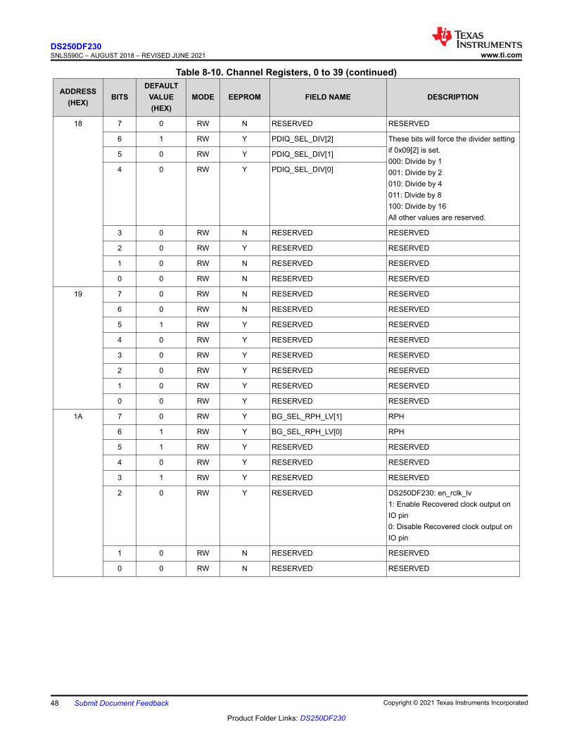
Table 8-10. Channel Registers, 0 to 39 (continued)
ADDRESS(HEX)
BITSDEFAULT
VALUE(HEX)
MODE EEPROM FIELD NAME DESCRIPTION
18 7 0 RW N RESERVED RESERVED
6 1 RW Y PDIQ_SEL_DIV[2] These bits will force the divider setting if 0x09[2] is set.000: Divide by 1001: Divide by 2010: Divide by 4011: Divide by 8100: Divide by 16All other values are reserved.
5 0 RW Y PDIQ_SEL_DIV[1]
4 0 RW Y PDIQ_SEL_DIV[0]
3 0 RW N RESERVED RESERVED
2 0 RW Y RESERVED RESERVED
1 0 RW N RESERVED RESERVED
0 0 RW N RESERVED RESERVED
19 7 0 RW N RESERVED RESERVED
6 0 RW N RESERVED RESERVED
5 1 RW Y RESERVED RESERVED
4 0 RW Y RESERVED RESERVED
3 0 RW Y RESERVED RESERVED
2 0 RW Y RESERVED RESERVED
1 0 RW Y RESERVED RESERVED
0 0 RW Y RESERVED RESERVED
1A 7 0 RW Y BG_SEL_RPH_LV[1] RPH
6 1 RW Y BG_SEL_RPH_LV[0] RPH
5 1 RW Y RESERVED RESERVED
4 0 RW Y RESERVED RESERVED
3 1 RW Y RESERVED RESERVED
2 0 RW Y RESERVED DS250DF230: en_rclk_lv1: Enable Recovered clock output on IO pin0: Disable Recovered clock output on IO pin
1 0 RW N RESERVED RESERVED
0 0 RW N RESERVED RESERVED
DS250DF230SNLS590C – AUGUST 2018 – REVISED JUNE 2021 www.ti.com
48 Submit Document Feedback Copyright © 2021 Texas Instruments Incorporated
Product Folder Links: DS250DF230

Table 8-10. Channel Registers, 0 to 39 (continued)
ADDRESS(HEX)
BITSDEFAULT
VALUE(HEX)
MODE EEPROM FIELD NAME DESCRIPTION
1B 7 0 RW N RESERVED RESERVED
6 0 RW N RESERVED RESERVED
5 0 RW N RESERVED RESERVED
4 0 RW N RESERVED RESERVED
3 0 RW N RESERVED RESERVED
2 0 RW N RESERVED RESERVED
1 1 RW Y CP_EN_CP_PD 1: Normal operation, phase detector charge pump enabled
0 1 RW Y CP_EN_CP_FD 1: Normal operation, frequency detector charge pump enabled
1C 7 1 RW Y EN_IDAC_PD_CP2 Phase detector charge pump setting. Override bit required for these bits to take effect
6 0 RW Y EN_IDAC_PD_CP1
5 0 RW Y EN_IDAC_PD_CP0
4 1 RW Y EN_IDAC_FD_CP2 Frequency detector charge pump setting. Override bit required for these bits to take effect
3 0 RW Y EN_IDAC_FD_CP1
2 0 RW Y EN_IDAC_FD_CP0
1 0 RW Y RESERVED RESERVED
0 0 RW Y RESERVED RESERVED
1D 7 0 RW N RESERVED RESERVED
6 0 RW N RESERVED RESERVED
5 0 RW N RESERVED RESERVED
4 0 RW N RESERVED RESERVED
3 0 RW N RESERVED RESERVED
2 0 RW N RESERVED RESERVED
1 0 RW N RESERVED RESERVED
0 0 RW N RESERVED RESERVED
www.ti.comDS250DF230
SNLS590C – AUGUST 2018 – REVISED JUNE 2021
Copyright © 2021 Texas Instruments Incorporated Submit Document Feedback 49
Product Folder Links: DS250DF230

Table 8-10. Channel Registers, 0 to 39 (continued)
ADDRESS(HEX)
BITSDEFAULT
VALUE(HEX)
MODE EEPROM FIELD NAME DESCRIPTION
1E 7 1 RW Y PFD_SEL_DATA_PRELCK[2] Output mode for when the CDR is not locked. For these values to take effect, Reg_0x09[5] must be set to 0, which is the default.000: Raw Data111: Mute (Default)All other values are reserved. (Refer to the Programming Guide for more details)
6 1 RW Y PFD_SEL_DATA_PRELCK[1]
5 1 RW Y PFD_SEL_DATA_PRELCK[0]
4 0 RW N SER_EN 1: Enable serializer (used for PRBS Generator)0: Normal operation. Disable serializer.
3 1 RW Y DFE_PD This bit must be cleared for the DFE to be functional in any adapt mode.1: (Default) DFE disabled.0: DFE enabled
2 0 RW Y PFD_PD_PD 1: Power down PFD phase detector.0: Normal operation. Enable PFD phase detector.
1 0 RW Y EN_PARTIAL_DFE 1: Enable DFE taps 3-5. DFE_PD must also be set to 0.0: (Default) Disable DFE taps 3-5.
0 1 RW Y PFD_EN_FD 1: Normal operation. Enable PFD frequency detector.0: Disable PFD frequency detector.
1F 7 0 RW N RESERVED RESERVED
6 0 RW N RESERVED RESERVED
5 0 RW N RESERVED RESERVED
4 0 RW Y RESERVED RESERVED
3 1 RW Y MR_LPF_AUTO_ADJST_EN 1: Normal operation. Allow LPF to tune to optimum value during fast-cap search routine.0: Otherwise LPF value is determined by the Reg_0x9D.
2 0 RW Y RESERVED RESERVED
1 1 RW Y RESERVED RESERVED
0 1 RW Y RESERVED RESERVED
DS250DF230SNLS590C – AUGUST 2018 – REVISED JUNE 2021 www.ti.com
50 Submit Document Feedback Copyright © 2021 Texas Instruments Incorporated
Product Folder Links: DS250DF230
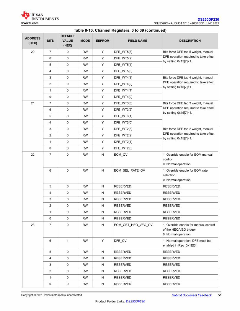
Table 8-10. Channel Registers, 0 to 39 (continued)
ADDRESS(HEX)
BITSDEFAULT
VALUE(HEX)
MODE EEPROM FIELD NAME DESCRIPTION
20 7 0 RW Y DFE_WT5[3] Bits force DFE tap 5 weight, manual DFE operation required to take effect by setting 0x15[7]=1.
6 0 RW Y DFE_WT5[2]
5 0 RW Y DFE_WT5[1]
4 0 RW Y DFE_WT5[0]
3 0 RW Y DFE_WT4[3] Bits force DFE tap 4 weight, manual DFE operation required to take effect by setting 0x15[7]=1.
2 0 RW Y DFE_WT4[2]
1 0 RW Y DFE_WT4[1]
0 0 RW Y DFE_WT4[0]
21 7 0 RW Y DFE_WT3[3] Bits force DFE tap 3 weight, manual DFE operation required to take effect by setting 0x15[7]=1.
6 0 RW Y DFE_WT3[2]
5 0 RW Y DFE_WT3[1]
4 0 RW Y DFE_WT3[0]
3 0 RW Y DFE_WT2[3] Bits force DFE tap 2 weight, manual DFE operation required to take effect by setting 0x15[7]=1.
2 0 RW Y DFE_WT2[2]
1 0 RW Y DFE_WT2[1]
0 0 RW Y DFE_WT2[0]
22 7 0 RW N EOM_OV 1: Override enable for EOM manual control0: Normal operation
6 0 RW N EOM_SEL_RATE_OV 1: Override enable for EOM rate selection0: Normal operation
5 0 RW N RESERVED RESERVED
4 0 RW N RESERVED RESERVED
3 0 RW N RESERVED RESERVED
2 0 RW N RESERVED RESERVED
1 0 RW N RESERVED RESERVED
0 0 RW N RESERVED RESERVED
23 7 0 RW N EOM_GET_HEO_VEO_OV 1: Override enable for manual control of the HEO/VEO trigger0: Normal operation
6 1 RW Y DFE_OV 1: Normal operation; DFE must be enabled in Reg_0x1E[3].
5 0 RW N RESERVED RESERVED
4 0 RW N RESERVED RESERVED
3 0 RW N RESERVED RESERVED
2 0 RW N RESERVED RESERVED
1 0 RW N RESERVED RESERVED
0 0 RW N RESERVED RESERVED
www.ti.comDS250DF230
SNLS590C – AUGUST 2018 – REVISED JUNE 2021
Copyright © 2021 Texas Instruments Incorporated Submit Document Feedback 51
Product Folder Links: DS250DF230

Table 8-10. Channel Registers, 0 to 39 (continued)
ADDRESS(HEX)
BITSDEFAULT
VALUE(HEX)
MODE EEPROM FIELD NAME DESCRIPTION
24 7 0 RW N FAST_EOM 1: Enables fast EOM for full eye capture. In this mode the phase DAC and voltage DAC or the EOM are automatically incremented through a 64 x 64 matrix. Values for each point are stored in Reg_0x25 and Reg_0x26.0: Normal operation.
6 0 R N DFE_EQ_ERROR_NO_LOCK DFE/CTLE SM quit due to loss of lock
5 0 R N GET_HEO_VEO_ERROR_NO_HITS
get_heo_veo sees no hits at zero crossing
4 0 R N GET_HEO_VEO_ERROR_NO_OPENING
get_heo_veo cannot see a vertical eye opening
3 0 RW N RESERVED RESERVED
2 0 RWSC N DFE_ADAPT 1: Manually start DFE adaption (self-clearing).0: Normal operation.
1 0 R N EOM_GET_HEO_VEO 1: Manually triggers HEO/VEO measurement; feature must be enabled with Reg_0x23[7]; the HEO/VEO values are read from Reg_0x27, Reg_0x28
0 0 RWSC N EOM_START 1: Starts EOM counter, self-clearing
25 7 0 R N EOM_COUNT15 MSBs of EOM counter
6 0 R N EOM_COUNT14
5 0 R N EOM_COUNT13
4 0 R N EOM_COUNT12
3 0 R N EOM_COUNT11
2 0 R N EOM_COUNT10
1 0 R N EOM_COUNT9
0 0 R N EOM_COUNT8
26 7 0 R N EOM_COUNT7 LSBs of EOM counter
6 0 R N EOM_COUNT6
5 0 R N EOM_COUNT5
4 0 R N EOM_COUNT4
3 0 R N EOM_COUNT3
2 0 R N EOM_COUNT2
1 0 R N EOM_COUNT1
0 0 R N EOM_COUNT0
DS250DF230SNLS590C – AUGUST 2018 – REVISED JUNE 2021 www.ti.com
52 Submit Document Feedback Copyright © 2021 Texas Instruments Incorporated
Product Folder Links: DS250DF230

Table 8-10. Channel Registers, 0 to 39 (continued)
ADDRESS(HEX)
BITSDEFAULT
VALUE(HEX)
MODE EEPROM FIELD NAME DESCRIPTION
27 7 0 R N HEO7 HEO value, requires CDR to be locked for valid measurement6 0 R N HEO6
5 0 R N HEO5
4 0 R N HEO4
3 0 R N HEO3
2 0 R N HEO2
1 0 R N HEO1
0 0 R N HEO0
28 7 0 R N VEO7 VEO value, requires CDR to be locked for valid measurement6 0 R N VEO6
5 0 R N VEO5
4 0 R N VEO4
3 0 R N VEO3
2 0 R N VEO2
1 0 R N VEO1
0 0 R N VEO0
29 7 0 RW N RESERVED RESERVED
6 0 R N EOM_VRANGE_SETTING[1] Read the currently set Eye Monitor Voltage Range:11 - +/-400mV10 - +/- 300mV01 - +/- 200mV00 - +/- 100mV"
5 0 R N EOM_VRANGE_SETTING[0]
4 0 RW N RESERVED RESERVED
3 0 RW N RESERVED RESERVED
2 0 RW N RESERVED RESERVED
1 0 R N VEO[8] VEO MSB value
0 0 R N HEO[8] HEO MSB value
www.ti.comDS250DF230
SNLS590C – AUGUST 2018 – REVISED JUNE 2021
Copyright © 2021 Texas Instruments Incorporated Submit Document Feedback 53
Product Folder Links: DS250DF230

Table 8-10. Channel Registers, 0 to 39 (continued)
ADDRESS(HEX)
BITSDEFAULT
VALUE(HEX)
MODE EEPROM FIELD NAME DESCRIPTION
2A 7 0 RW Y EOM_TIMER_THR[3] The value of EOM_TIMER_THR[7:4] controls the amount of time the Eye Monitor samples each point in the eye.(Refer to the Programming Guide for more details)
6 1 RW Y EOM_TIMER_THR[2]
5 0 RW Y EOM_TIMER_THR[1]
4 1 RW Y EOM_TIMER_THR[0]
3 1 RW Y VEO_MIN_REQ_HITS[3] Whenever the Eye Monitor is used to measure HEO and VEO, the data is sampled for some number of bits, set by Reg_0x2A[7:4]. This register sets the number of hits within that sample size that is required before the EOM will indicate a hit has occurred. This filtering only affects the VEO measurement.
2 0 RW Y VEO_MIN_REQ_HITS[2]
1 1 RW Y VEO_MIN_REQ_HITS[1]
0 0 RW Y VEO_MIN_REQ_HITS[0]
2B 7 0 RW N RESERVED RESERVED
6 0 RW N RESERVED RESERVED
5 0 RW Y RESERVED RESERVED
4 0 RW Y RESERVED RESERVED
3 1 RW Y EOM_MIN_REQ_HITS[3] Whenever the Eye Monitor is used to measure HEO and VEO, the data is sampled for some number of bits, set by Reg_0x2A[7:4]. This register sets the number of hits within that sample size that is required before the EOM will indicate a hit has occurred. This filtering only affects the HEO measurement.
2 0 RW Y EOM_MIN_REQ_HITS[2]
1 1 RW Y EOM_MIN_REQ_HITS[1]
0 0 RW Y EOM_MIN_REQ_HITS[0]
2C 7 1 RW N RELOAD_DFE_TAPS Causes DFE taps to load from last adapted values
6 1 RW Y VEO_SCALE 1: Normal operation. Scale VEO based on EOM vrange.
5 1 RW Y DFE_SM_FOM1 This register defines the Figure of Merit used when adapting the DFE:00: not valid01: SM uses only HEO10: SM uses only VEO11: SM uses both HEO and VEOAdditionally, if Reg_0x6E[6] is set to '1', the Alternate FOM is used. This bit takes precedence over DFE_SM_FOM
4 1 RW Y DFE_SM_FOM0
3 0 RW Y DFE_ADAPT_COUNTER[3] DFE look-beyond count.
2 1 RW Y DFE_ADAPT_COUNTER[2]
1 1 RW Y DFE_ADAPT_COUNTER[1]
0 0 RW Y DFE_ADAPT_COUNTER[0]
DS250DF230SNLS590C – AUGUST 2018 – REVISED JUNE 2021 www.ti.com
54 Submit Document Feedback Copyright © 2021 Texas Instruments Incorporated
Product Folder Links: DS250DF230

Table 8-10. Channel Registers, 0 to 39 (continued)
ADDRESS(HEX)
BITSDEFAULT
VALUE(HEX)
MODE EEPROM FIELD NAME DESCRIPTION
2D 7 0 RW Y RESERVED RESERVED
6 0 RW Y RESERVED RESERVED
5 1 RW Y RESERVED RESERVED
4 1 RW Y RESERVED RESERVED
3 0 RW Y REG_EQ_BST_OV 1: Allow override control of the EQ setting by writing to Reg_0x030: Normal operation.
2 0 RW Y RESERVED DS250DF230:1: Set CTLE bypass Enabled when REG_RQ_BST_OV=10: Normal operation.
1 0 RW Y RESERVED RESERVED
0 0 RW Y RESERVED RESERVED
2E 7 0 RW N RESERVED RESERVED
6 0 RW N RESERVED RESERVED
5 0 R N EQ_BST3_BIT2_TO_EQ Read-back of eq_BST3[2] driving the EQ
4 0 RW N RESERVED RESERVED
3 0 RW N RESERVED RESERVED
2 0 RW N PRBS_PATTERN_SEL[2] MSB for the PRBS_PATTERN_SEL field. Lower bits are found on Reg_0x30[1:0]. Refer to the Reg_0x30 description on this table.
1 0 RW N RESERVED RESERVED
0 0 RW N RESERVED RESERVED
www.ti.comDS250DF230
SNLS590C – AUGUST 2018 – REVISED JUNE 2021
Copyright © 2021 Texas Instruments Incorporated Submit Document Feedback 55
Product Folder Links: DS250DF230
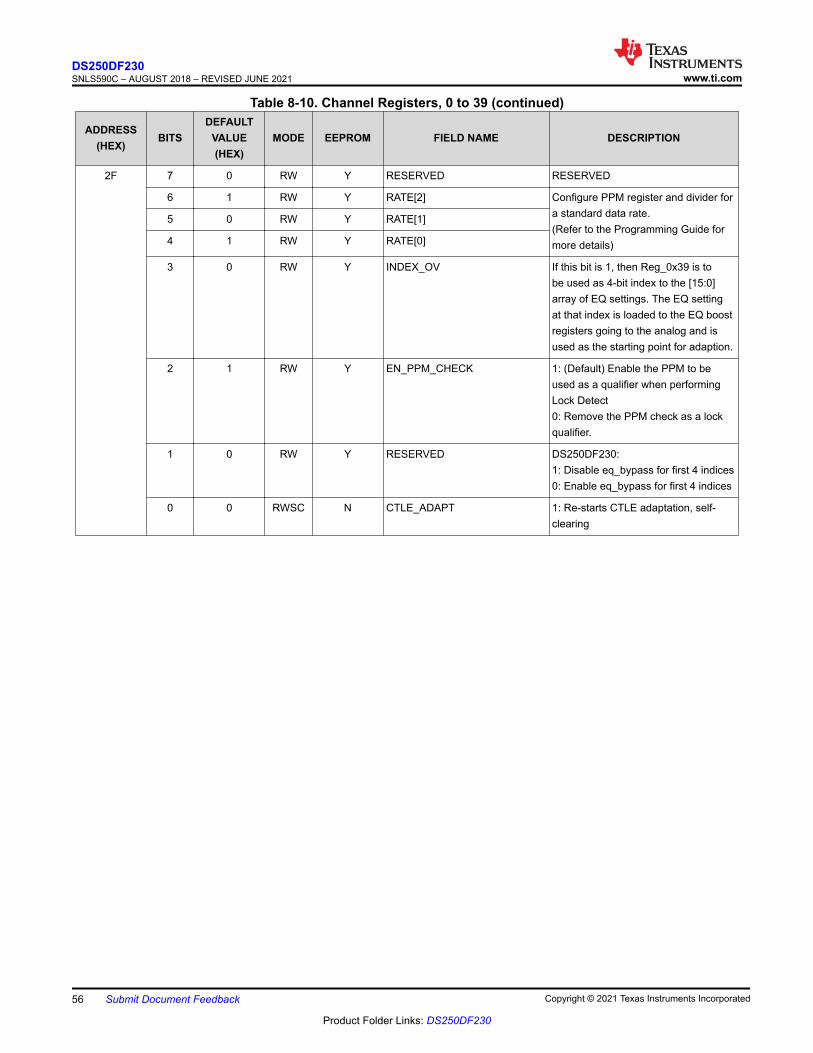
Table 8-10. Channel Registers, 0 to 39 (continued)
ADDRESS(HEX)
BITSDEFAULT
VALUE(HEX)
MODE EEPROM FIELD NAME DESCRIPTION
2F 7 0 RW Y RESERVED RESERVED
6 1 RW Y RATE[2] Configure PPM register and divider for a standard data rate.(Refer to the Programming Guide for more details)
5 0 RW Y RATE[1]
4 1 RW Y RATE[0]
3 0 RW Y INDEX_OV If this bit is 1, then Reg_0x39 is to be used as 4-bit index to the [15:0] array of EQ settings. The EQ setting at that index is loaded to the EQ boost registers going to the analog and is used as the starting point for adaption.
2 1 RW Y EN_PPM_CHECK 1: (Default) Enable the PPM to be used as a qualifier when performing Lock Detect0: Remove the PPM check as a lock qualifier.
1 0 RW Y RESERVED DS250DF230:1: Disable eq_bypass for first 4 indices0: Enable eq_bypass for first 4 indices
0 0 RWSC N CTLE_ADAPT 1: Re-starts CTLE adaptation, self-clearing
DS250DF230SNLS590C – AUGUST 2018 – REVISED JUNE 2021 www.ti.com
56 Submit Document Feedback Copyright © 2021 Texas Instruments Incorporated
Product Folder Links: DS250DF230
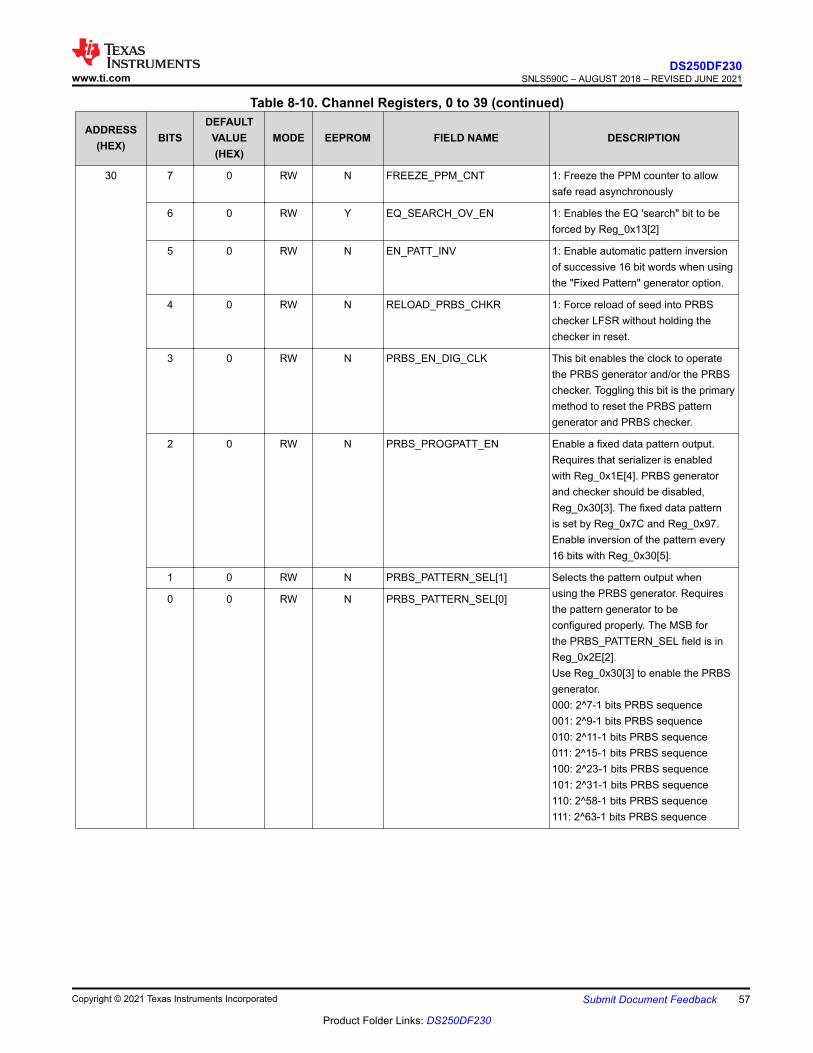
Table 8-10. Channel Registers, 0 to 39 (continued)
ADDRESS(HEX)
BITSDEFAULT
VALUE(HEX)
MODE EEPROM FIELD NAME DESCRIPTION
30 7 0 RW N FREEZE_PPM_CNT 1: Freeze the PPM counter to allow safe read asynchronously
6 0 RW Y EQ_SEARCH_OV_EN 1: Enables the EQ 'search" bit to be forced by Reg_0x13[2]
5 0 RW N EN_PATT_INV 1: Enable automatic pattern inversion of successive 16 bit words when using the "Fixed Pattern" generator option.
4 0 RW N RELOAD_PRBS_CHKR 1: Force reload of seed into PRBS checker LFSR without holding the checker in reset.
3 0 RW N PRBS_EN_DIG_CLK This bit enables the clock to operate the PRBS generator and/or the PRBS checker. Toggling this bit is the primary method to reset the PRBS pattern generator and PRBS checker.
2 0 RW N PRBS_PROGPATT_EN Enable a fixed data pattern output. Requires that serializer is enabled with Reg_0x1E[4]. PRBS generator and checker should be disabled, Reg_0x30[3]. The fixed data pattern is set by Reg_0x7C and Reg_0x97. Enable inversion of the pattern every 16 bits with Reg_0x30[5].
1 0 RW N PRBS_PATTERN_SEL[1] Selects the pattern output when using the PRBS generator. Requires the pattern generator to be configured properly. The MSB for the PRBS_PATTERN_SEL field is in Reg_0x2E[2].Use Reg_0x30[3] to enable the PRBS generator.000: 2^7-1 bits PRBS sequence001: 2^9-1 bits PRBS sequence010: 2^11-1 bits PRBS sequence011: 2^15-1 bits PRBS sequence100: 2^23-1 bits PRBS sequence101: 2^31-1 bits PRBS sequence110: 2^58-1 bits PRBS sequence111: 2^63-1 bits PRBS sequence
0 0 RW N PRBS_PATTERN_SEL[0]
www.ti.comDS250DF230
SNLS590C – AUGUST 2018 – REVISED JUNE 2021
Copyright © 2021 Texas Instruments Incorporated Submit Document Feedback 57
Product Folder Links: DS250DF230

Table 8-10. Channel Registers, 0 to 39 (continued)
ADDRESS(HEX)
BITSDEFAULT
VALUE(HEX)
MODE EEPROM FIELD NAME DESCRIPTION
31 7 0 RW N PRBS_INT_EN 1: Enables interrupt for detection of PRBS errors. The PRBS checker must be properly configured for this feature to work.
6 0 RW Y ADAPT_MODE[1] 00: no adaption01: adapt CTLE only10: adapt CTLE until optimal, then DFE, then CTLE again11: adapt CTLE until lock, then DFE, then EQ until optimalNote: for ADAPT_MODE=2 or 3, the DFE must be enabled by setting Reg_0x1E[3]=0 and Reg_0x1E[1]=1.(Refer to the Programming Guide for more details)
5 1 RW Y ADAPT_MODE[0]
4 0 RW Y EQ_SM_FOM[1] CTLE (EQ) adaption state machine figure of merit.00: (Default) SM uses both HEO and VEO01: SM uses HEO only10: SM uses VEO only11: SM uses both HEO and VEOAdditionally, if Reg_0x6E[7]=1, the Alternate FOM is used. Reg_0x6E[7] takes precedence over EQ_SM_FOM.
3 0 RW Y EQ_SM_FOM[0]
2 0 RW N RESERVED RESERVED
1 0 RW Y CDR_LOCK_LOSS_INT_EN Enable for CDR Lock Loss Interrupt. Observable in Reg_0x01[5]
0 0 RW Y SIGNAL_DET_LOSS_INT_EN Enable for Signal Detect Loss Interrupt. Observable in Reg_0x01[0]
32 7 0 RW Y HEO_INT_THRESH[3] These bits set the threshold for the HEO and VEO interrupt. Each threshold bit represents 8 counts of HEO or VEO.
6 0 RW Y HEO_INT_THRESH[2]
5 0 RW Y HEO_INT_THRESH[1]
4 1 RW Y HEO_INT_THRESH[0]
3 0 RW Y VEO_INT_THRESH[3]
2 0 RW Y VEO_INT_THRESH[2]
1 0 RW Y VEO_INT_THRESH[1]
0 1 RW Y VEO_INT_THRESH[0]
DS250DF230SNLS590C – AUGUST 2018 – REVISED JUNE 2021 www.ti.com
58 Submit Document Feedback Copyright © 2021 Texas Instruments Incorporated
Product Folder Links: DS250DF230

Table 8-10. Channel Registers, 0 to 39 (continued)
ADDRESS(HEX)
BITSDEFAULT
VALUE(HEX)
MODE EEPROM FIELD NAME DESCRIPTION
33 7 1 RW Y HEO_THRESH[3] In adapt mode 3, the register sets the minimum HEO and VEO required for CTLE adaption, before starting DFE adaption. This can be a max of 15.
6 0 RW Y HEO_THRESH[2]
5 0 RW Y HEO_THRESH[1]
4 0 RW Y HEO_THRESH[0]
3 1 RW Y VEO_THRESH[3]
2 0 RW Y VEO_THRESH[2]
1 0 RW Y VEO_THRESH[1]
0 0 RW Y VEO_THRESH[0]
34 7 0 R N PPM_ERR_RDY 1: Indicates that a PPM error count is read to be read from channel Reg_0x3B and Reg_0x3C
6 0 RW Y LOW_POWER_MODE_DISABLE By default, all blocks (except signal detect) power down after 100 ms after signal detect goes low. If set high, all blocks get powered on after the signal detect initially goes high.
5 1 RW Y LOCK_COUNTER[1] After achieving lock, the CDR continues to monitor the lock criteria. If the lock criteria fail, the lock is checked for a total of N number of times before declaring an out of lock condition, where N is set by this the value in these registers, with a max value of +3, for a total of 4. If during the N lock checks, lock is regained, then the lock condition is left HI, and the counter is reset back to zero.
4 1 RW Y LOCK_COUNTER[0]
3 1 RW Y DFE_MAX_TAP2_5[3] These four bits are used to set the maximum value by which DFE taps 2-5 are able to adapt with each subsequent adaptation. Same used for both polarities.
2 1 RW Y DFE_MAX_TAP2_5[2]
1 1 RW Y DFE_MAX_TAP2_5[1]
0 1 RW Y DFE_MAX_TAP2_5[0]
www.ti.comDS250DF230
SNLS590C – AUGUST 2018 – REVISED JUNE 2021
Copyright © 2021 Texas Instruments Incorporated Submit Document Feedback 59
Product Folder Links: DS250DF230

Table 8-10. Channel Registers, 0 to 39 (continued)
ADDRESS(HEX)
BITSDEFAULT
VALUE(HEX)
MODE EEPROM FIELD NAME DESCRIPTION
35 7 0 RW Y DATA_LOCK_PPM[1] Modifies the value of the PPM delta tolerance from channel Reg_0x64:00 - ppm_delta[7:0] =1 x ppm_delta[7:0]01 - ppm_delta[7:0] =1 x ppm_delta[7:0] + ppm_delta[3:1]10 - ppm_delta[7:0] =2 x ppm_delta[7:0]11 - ppm_delta[7:0] =2 x ppm_delta[7:0] + ppm_delta[3:1]
6 0 RW Y DATA_LOCK_PPM[0]
5 0 RW N GET_PPM_ERROR Get PPM error from PPM_COUNT - clears when done. Normally updates continuously, but can be manually triggered with read value from Reg_0x3B and Reg_0x3C
4 0 RW Y DFE_MAX_TAP1[4] Limits DFE tap 1 maximum magnitude.
3 1 RW Y DFE_MAX_TAP1[3]
2 1 RW Y DFE_MAX_TAP1[2]
1 1 RW Y DFE_MAX_TAP1[1]
0 1 RW Y DFE_MAX_TAP1[0]
36 7 0 RW N RESERVED RESERVED
6 0 RW Y HEO_VEO_INT_EN 1: Enable HEO/VEO interrupt capability
5 1 RW Y REF_MODE[1] 11: Normal Operation. Refererence mode 3.4 1 RW Y REF_MODE[0]
3 0 RW N RESERVED RESERVED
2 0 RW Y RESERVED RESERVED
1 0 RW N RESERVED RESERVED
0 0 RW N RESERVED RESERVED
37 7 0 R N CTLE_STATUS[7] Feature is reserved for future use
6 0 R N CTLE_STATUS[6]
5 0 R N CTLE_STATUS[5]
4 0 R N CTLE_STATUS[4]
3 0 R N CTLE_STATUS[3]
2 0 R N CTLE_STATUS[2]
1 0 R N CTLE_STATUS[1]
0 0 R N CTLE_STATUS[0]
DS250DF230SNLS590C – AUGUST 2018 – REVISED JUNE 2021 www.ti.com
60 Submit Document Feedback Copyright © 2021 Texas Instruments Incorporated
Product Folder Links: DS250DF230
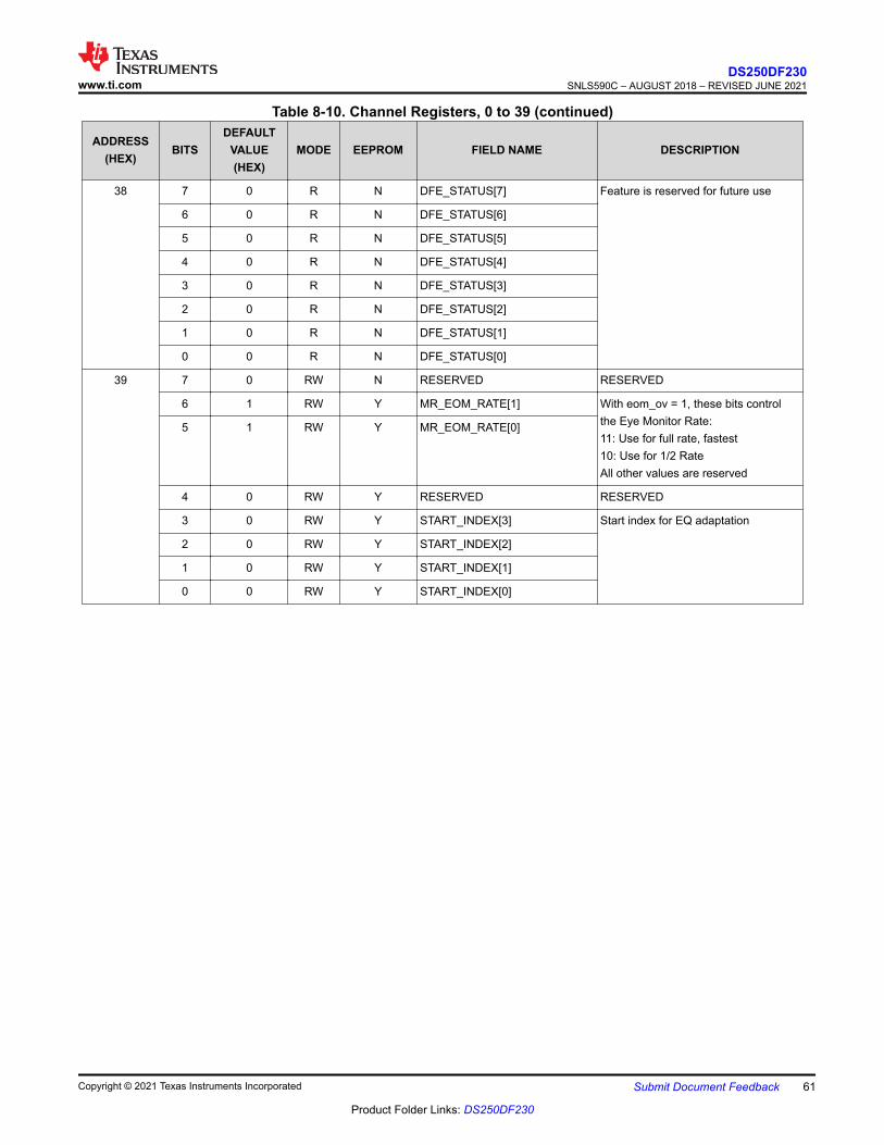
Table 8-10. Channel Registers, 0 to 39 (continued)
ADDRESS(HEX)
BITSDEFAULT
VALUE(HEX)
MODE EEPROM FIELD NAME DESCRIPTION
38 7 0 R N DFE_STATUS[7] Feature is reserved for future use
6 0 R N DFE_STATUS[6]
5 0 R N DFE_STATUS[5]
4 0 R N DFE_STATUS[4]
3 0 R N DFE_STATUS[3]
2 0 R N DFE_STATUS[2]
1 0 R N DFE_STATUS[1]
0 0 R N DFE_STATUS[0]
39 7 0 RW N RESERVED RESERVED
6 1 RW Y MR_EOM_RATE[1] With eom_ov = 1, these bits control the Eye Monitor Rate:11: Use for full rate, fastest10: Use for 1/2 RateAll other values are reserved
5 1 RW Y MR_EOM_RATE[0]
4 0 RW Y RESERVED RESERVED
3 0 RW Y START_INDEX[3] Start index for EQ adaptation
2 0 RW Y START_INDEX[2]
1 0 RW Y START_INDEX[1]
0 0 RW Y START_INDEX[0]
www.ti.comDS250DF230
SNLS590C – AUGUST 2018 – REVISED JUNE 2021
Copyright © 2021 Texas Instruments Incorporated Submit Document Feedback 61
Product Folder Links: DS250DF230

Table 8-11. Channel Registers, 3A to A9
ADDRESS(Hex)
BITSDEFAULT
VALUE(Hex)
MODE EEPROM FIELD NAME DESCRIPTION
3A 7 0 RW Y FIXED_EQ_BST0[1] During adaptation, if the divider setting is >2, then a fixed EQ setting from this register will be used. However, if channel Reg_0x6F[7] is enabled, then an EQ adaptation will be performed instead
6 0 RW Y FIXED_EQ_BST0[0]
5 0 RW Y FIXED_EQ_BST1[1]
4 0 RW Y FIXED_EQ_BST1[0]
3 0 RW Y FIXED_EQ_BST2[1]
2 0 RW Y FIXED_EQ_BST2[0]
1 0 RW Y FIXED_EQ_BST3[1]
0 0 RW Y FIXED_EQ_BST3[0]
3B 7 0 R N PPM_COUNT[15] PPM count MSB
6 0 R N PPM_COUNT[14]
5 0 R N PPM_COUNT[13]
4 0 R N PPM_COUNT[12]
3 0 R N PPM_COUNT[11]
2 0 R N PPM_COUNT[10]
1 0 R N PPM_COUNT[9]
0 0 R N PPM_COUNT[8]
3C 7 0 R N PPM_COUNT[7] PPM count LSB
6 0 R N PPM_COUNT[6]
5 0 R N PPM_COUNT[5]
4 0 R N PPM_COUNT[4]
3 0 R N PPM_COUNT[3]
2 0 R N PPM_COUNT[2]
1 0 R N PPM_COUNT[1]
0 0 R N PPM_COUNT[0]
3D 7 0 RW Y EN_FIR_CURSOR 1: Enable Pre- and Post-cursor FIR0: Disable Pre- and Post-cursor FIR (lower power)
6 0 RW Y FIR_C0_SGN Main-cursor sign bit0: positive1: negative
5 0 RW Y DRV_SEL_LOW_RATE_LV 0: Default1: Slow slew rate. Not recommended for divided-by-1 data rates
4 1 RW Y FIR_C0[4] Main-cursor magnitude(Refer to the Programming Guide for more details)
3 1 RW Y FIR_C0[3]
2 0 RW Y FIR_C0[2]
1 1 RW Y FIR_C0[1]
0 0 RW Y FIR_C0[0]
DS250DF230SNLS590C – AUGUST 2018 – REVISED JUNE 2021 www.ti.com
62 Submit Document Feedback Copyright © 2021 Texas Instruments Incorporated
Product Folder Links: DS250DF230

Table 8-11. Channel Registers, 3A to A9 (continued)
ADDRESS(Hex)
BITSDEFAULT
VALUE(Hex)
MODE EEPROM FIELD NAME DESCRIPTION
3E 7 0 RW Y FIR_PD_TX
6 1 RW Y FIR_CN1_SGN Pre-cursor sign bit1: negative0: positive
5 0 RW Y RESERVED RESERVED
4 0 RW Y RESERVED RESERVED
3 0 RW Y FIR_CN1[3] Pre-cursor magnitude(Refer to the Programming Guide for more details)
2 0 RW Y FIR_CN1[2]
1 0 RW Y FIR_CN1[1]
0 0 RW Y FIR_CN1[0]
3F 7 0 RW Y RESERVED RESERVED
6 1 RW Y FIR_CP1_SGN Post-cursor sign bit1: negative0: positive
5 0 RW Y RESERVED DS250DF230: rclk_sel_div_lv[1]Valid only inconjuction with mr_cipri_clk_div_sel_ov; Otherwise decoded from rate tableAnalog Div Digital Div00: 30 1101: 32 1010: 36 1111: 40 10
4 0 RW Y RESERVED DS250DF230: rclk_sel_div_lv[0], see more on MSB description
3 0 RW Y FIR_CP1[3] Post-cursor magnitude(Refer to the Programming Guide for more details)
2 0 RW Y FIR_CP1[2]
1 0 RW Y FIR_CP1[1]
0 0 RW Y FIR_CP1[0]
40 7 0 RW Y EQ_ARRAY_INDEX_0_BST0[1] DS250DF230: The first four indices use enable_byapss=1.
6 0 RW Y EQ_ARRAY_INDEX_0_BST0[0]
5 0 RW Y EQ_ARRAY_INDEX_0_BST1[1]
4 0 RW Y EQ_ARRAY_INDEX_0_BST1[0]
3 0 RW Y EQ_ARRAY_INDEX_0_BST2[1]
2 0 RW Y EQ_ARRAY_INDEX_0_BST2[0]
1 0 RW Y EQ_ARRAY_INDEX_0_BST3[1]
0 0 RW Y EQ_ARRAY_INDEX_0_BST3[0] DS250DF230: Reg_0x40=0x00
www.ti.comDS250DF230
SNLS590C – AUGUST 2018 – REVISED JUNE 2021
Copyright © 2021 Texas Instruments Incorporated Submit Document Feedback 63
Product Folder Links: DS250DF230

Table 8-11. Channel Registers, 3A to A9 (continued)
ADDRESS(Hex)
BITSDEFAULT
VALUE(Hex)
MODE EEPROM FIELD NAME DESCRIPTION
41 7 0 RW Y EQ_ARRAY_INDEX_1_BST0[1]
6 0 RW Y EQ_ARRAY_INDEX_1_BST0[0]
5 0 RW Y EQ_ARRAY_INDEX_1_BST1[1]
4 0 RW Y EQ_ARRAY_INDEX_1_BST1[0]
3 0 RW Y EQ_ARRAY_INDEX_1_BST2[1]
2 0 RW Y EQ_ARRAY_INDEX_1_BST2[0]
1 0 RW Y EQ_ARRAY_INDEX_1_BST3[1]
0 1 RW Y EQ_ARRAY_INDEX_1_BST3[0] DS250DF230: Reg_0x41=0x01
42 7 0 RW Y EQ_ARRAY_INDEX_2_BST0[1]
6 0 RW Y EQ_ARRAY_INDEX_2_BST0[0]
5 0 RW Y EQ_ARRAY_INDEX_2_BST1[1]
4 0 RW Y EQ_ARRAY_INDEX_2_BST1[0]
3 0 RW Y EQ_ARRAY_INDEX_2_BST2[1]
2 0 RW Y EQ_ARRAY_INDEX_2_BST2[0]
1 1 RW Y EQ_ARRAY_INDEX_2_BST3[1]
0 0 RW Y EQ_ARRAY_INDEX_2_BST3[0] DS250DF230: Reg_0x42=0x02
43 7 0 RW Y EQ_ARRAY_INDEX_3_BST0[1]
6 0 RW Y EQ_ARRAY_INDEX_3_BST0[0]
5 0 RW Y EQ_ARRAY_INDEX_3_BST1[1]
4 0 RW Y EQ_ARRAY_INDEX_3_BST1[0]
3 0 RW Y EQ_ARRAY_INDEX_3_BST2[1]
2 0 RW Y EQ_ARRAY_INDEX_3_BST2[0]
1 1 RW Y EQ_ARRAY_INDEX_3_BST3[1]
0 1 RW Y EQ_ARRAY_INDEX_3_BST3[0] DS250DF230: Reg_0x43=0x03
44 7 0 RW Y EQ_ARRAY_INDEX_4_BST0[1]
6 0 RW Y EQ_ARRAY_INDEX_4_BST0[0]
5 0 RW Y EQ_ARRAY_INDEX_4_BST1[1]
4 0 RW Y EQ_ARRAY_INDEX_4_BST1[0]
3 0 RW Y EQ_ARRAY_INDEX_4_BST2[1]
2 0 RW Y EQ_ARRAY_INDEX_4_BST2[0]
1 0 RW Y EQ_ARRAY_INDEX_4_BST3[1]
0 0 RW Y EQ_ARRAY_INDEX_4_BST3[0] DS250DF230: Reg_0x44=0x00
DS250DF230SNLS590C – AUGUST 2018 – REVISED JUNE 2021 www.ti.com
64 Submit Document Feedback Copyright © 2021 Texas Instruments Incorporated
Product Folder Links: DS250DF230
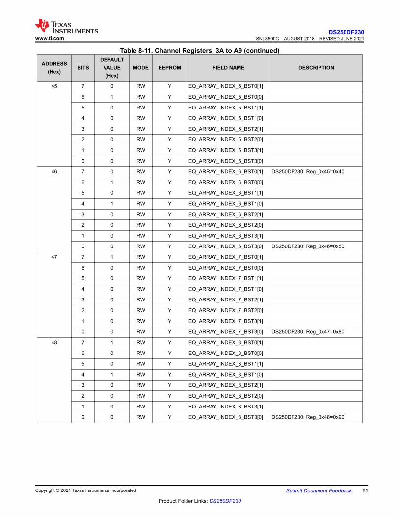
Table 8-11. Channel Registers, 3A to A9 (continued)
ADDRESS(Hex)
BITSDEFAULT
VALUE(Hex)
MODE EEPROM FIELD NAME DESCRIPTION
45 7 0 RW Y EQ_ARRAY_INDEX_5_BST0[1]
6 1 RW Y EQ_ARRAY_INDEX_5_BST0[0]
5 0 RW Y EQ_ARRAY_INDEX_5_BST1[1]
4 0 RW Y EQ_ARRAY_INDEX_5_BST1[0]
3 0 RW Y EQ_ARRAY_INDEX_5_BST2[1]
2 0 RW Y EQ_ARRAY_INDEX_5_BST2[0]
1 0 RW Y EQ_ARRAY_INDEX_5_BST3[1]
0 0 RW Y EQ_ARRAY_INDEX_5_BST3[0]
46 7 0 RW Y EQ_ARRAY_INDEX_6_BST0[1] DS250DF230: Reg_0x45=0x40
6 1 RW Y EQ_ARRAY_INDEX_6_BST0[0]
5 0 RW Y EQ_ARRAY_INDEX_6_BST1[1]
4 1 RW Y EQ_ARRAY_INDEX_6_BST1[0]
3 0 RW Y EQ_ARRAY_INDEX_6_BST2[1]
2 0 RW Y EQ_ARRAY_INDEX_6_BST2[0]
1 0 RW Y EQ_ARRAY_INDEX_6_BST3[1]
0 0 RW Y EQ_ARRAY_INDEX_6_BST3[0] DS250DF230: Reg_0x46=0x50
47 7 1 RW Y EQ_ARRAY_INDEX_7_BST0[1]
6 0 RW Y EQ_ARRAY_INDEX_7_BST0[0]
5 0 RW Y EQ_ARRAY_INDEX_7_BST1[1]
4 0 RW Y EQ_ARRAY_INDEX_7_BST1[0]
3 0 RW Y EQ_ARRAY_INDEX_7_BST2[1]
2 0 RW Y EQ_ARRAY_INDEX_7_BST2[0]
1 0 RW Y EQ_ARRAY_INDEX_7_BST3[1]
0 0 RW Y EQ_ARRAY_INDEX_7_BST3[0] DS250DF230: Reg_0x47=0x80
48 7 1 RW Y EQ_ARRAY_INDEX_8_BST0[1]
6 0 RW Y EQ_ARRAY_INDEX_8_BST0[0]
5 0 RW Y EQ_ARRAY_INDEX_8_BST1[1]
4 1 RW Y EQ_ARRAY_INDEX_8_BST1[0]
3 0 RW Y EQ_ARRAY_INDEX_8_BST2[1]
2 0 RW Y EQ_ARRAY_INDEX_8_BST2[0]
1 0 RW Y EQ_ARRAY_INDEX_8_BST3[1]
0 0 RW Y EQ_ARRAY_INDEX_8_BST3[0] DS250DF230: Reg_0x48=0x90
www.ti.comDS250DF230
SNLS590C – AUGUST 2018 – REVISED JUNE 2021
Copyright © 2021 Texas Instruments Incorporated Submit Document Feedback 65
Product Folder Links: DS250DF230
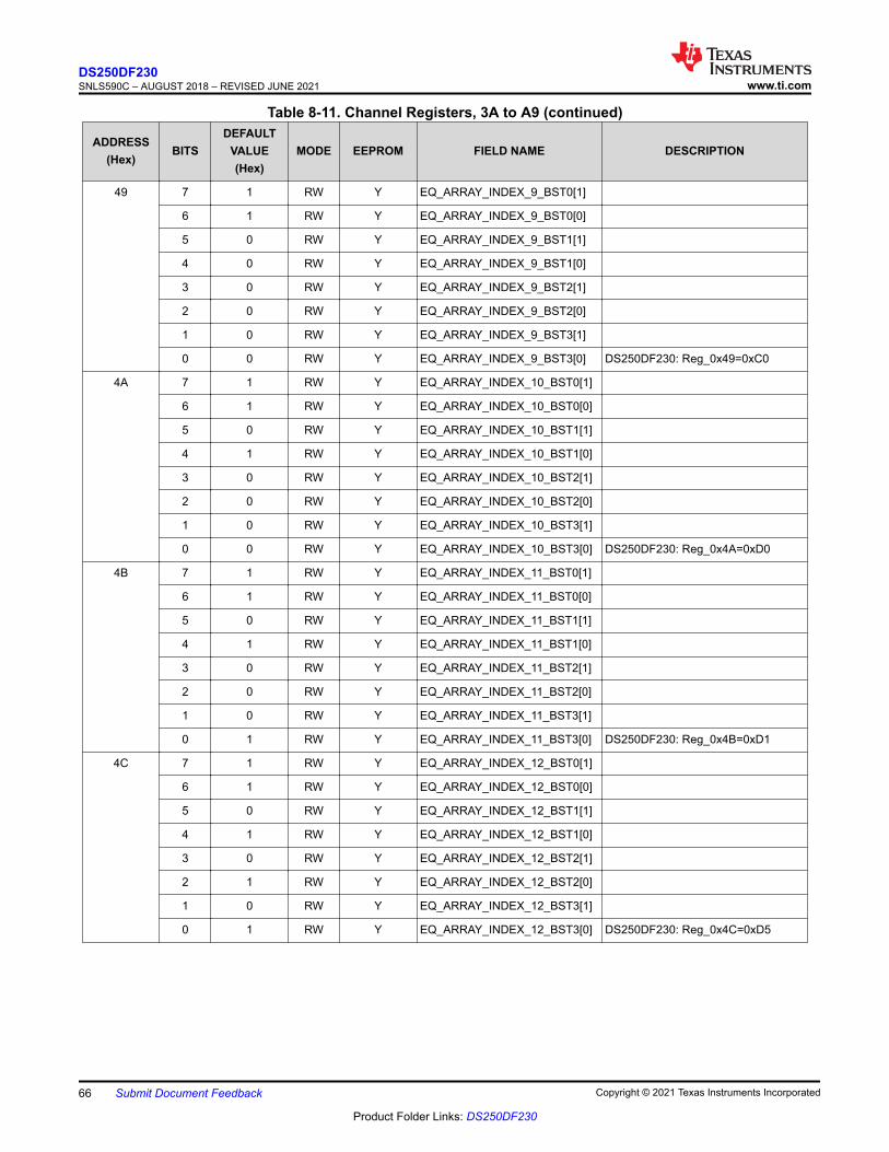
Table 8-11. Channel Registers, 3A to A9 (continued)
ADDRESS(Hex)
BITSDEFAULT
VALUE(Hex)
MODE EEPROM FIELD NAME DESCRIPTION
49 7 1 RW Y EQ_ARRAY_INDEX_9_BST0[1]
6 1 RW Y EQ_ARRAY_INDEX_9_BST0[0]
5 0 RW Y EQ_ARRAY_INDEX_9_BST1[1]
4 0 RW Y EQ_ARRAY_INDEX_9_BST1[0]
3 0 RW Y EQ_ARRAY_INDEX_9_BST2[1]
2 0 RW Y EQ_ARRAY_INDEX_9_BST2[0]
1 0 RW Y EQ_ARRAY_INDEX_9_BST3[1]
0 0 RW Y EQ_ARRAY_INDEX_9_BST3[0] DS250DF230: Reg_0x49=0xC0
4A 7 1 RW Y EQ_ARRAY_INDEX_10_BST0[1]
6 1 RW Y EQ_ARRAY_INDEX_10_BST0[0]
5 0 RW Y EQ_ARRAY_INDEX_10_BST1[1]
4 1 RW Y EQ_ARRAY_INDEX_10_BST1[0]
3 0 RW Y EQ_ARRAY_INDEX_10_BST2[1]
2 0 RW Y EQ_ARRAY_INDEX_10_BST2[0]
1 0 RW Y EQ_ARRAY_INDEX_10_BST3[1]
0 0 RW Y EQ_ARRAY_INDEX_10_BST3[0] DS250DF230: Reg_0x4A=0xD0
4B 7 1 RW Y EQ_ARRAY_INDEX_11_BST0[1]
6 1 RW Y EQ_ARRAY_INDEX_11_BST0[0]
5 0 RW Y EQ_ARRAY_INDEX_11_BST1[1]
4 1 RW Y EQ_ARRAY_INDEX_11_BST1[0]
3 0 RW Y EQ_ARRAY_INDEX_11_BST2[1]
2 0 RW Y EQ_ARRAY_INDEX_11_BST2[0]
1 0 RW Y EQ_ARRAY_INDEX_11_BST3[1]
0 1 RW Y EQ_ARRAY_INDEX_11_BST3[0] DS250DF230: Reg_0x4B=0xD1
4C 7 1 RW Y EQ_ARRAY_INDEX_12_BST0[1]
6 1 RW Y EQ_ARRAY_INDEX_12_BST0[0]
5 0 RW Y EQ_ARRAY_INDEX_12_BST1[1]
4 1 RW Y EQ_ARRAY_INDEX_12_BST1[0]
3 0 RW Y EQ_ARRAY_INDEX_12_BST2[1]
2 1 RW Y EQ_ARRAY_INDEX_12_BST2[0]
1 0 RW Y EQ_ARRAY_INDEX_12_BST3[1]
0 1 RW Y EQ_ARRAY_INDEX_12_BST3[0] DS250DF230: Reg_0x4C=0xD5
DS250DF230SNLS590C – AUGUST 2018 – REVISED JUNE 2021 www.ti.com
66 Submit Document Feedback Copyright © 2021 Texas Instruments Incorporated
Product Folder Links: DS250DF230

Table 8-11. Channel Registers, 3A to A9 (continued)
ADDRESS(Hex)
BITSDEFAULT
VALUE(Hex)
MODE EEPROM FIELD NAME DESCRIPTION
4D 7 1 RW Y EQ_ARRAY_INDEX_13_BST0[1]
6 1 RW Y EQ_ARRAY_INDEX_13_BST0[0]
5 0 RW Y EQ_ARRAY_INDEX_13_BST1[1]
4 1 RW Y EQ_ARRAY_INDEX_13_BST1[0]
3 1 RW Y EQ_ARRAY_INDEX_13_BST2[1]
2 0 RW Y EQ_ARRAY_INDEX_13_BST2[0]
1 0 RW Y EQ_ARRAY_INDEX_13_BST3[1]
0 0 RW Y EQ_ARRAY_INDEX_13_BST3[0] DS250DF230: Reg_0x4D=0xD8
4E 7 1 RW Y EQ_ARRAY_INDEX_14_BST0[1]
6 1 RW Y EQ_ARRAY_INDEX_14_BST0[0]
5 1 RW Y EQ_ARRAY_INDEX_14_BST1[1]
4 0 RW Y EQ_ARRAY_INDEX_14_BST1[0]
3 1 RW Y EQ_ARRAY_INDEX_14_BST2[1]
2 0 RW Y EQ_ARRAY_INDEX_14_BST2[0]
1 1 RW Y EQ_ARRAY_INDEX_14_BST3[1]
0 0 RW Y EQ_ARRAY_INDEX_14_BST3[0] DS250DF230: Reg_0x4E=0xEA
4F 7 1 RW Y EQ_ARRAY_INDEX_15_BST0[1]
6 1 RW Y EQ_ARRAY_INDEX_15_BST0[0]
5 1 RW Y EQ_ARRAY_INDEX_15_BST1[1]
4 1 RW Y EQ_ARRAY_INDEX_15_BST1[0]
3 0 RW Y EQ_ARRAY_INDEX_15_BST2[1]
2 1 RW Y EQ_ARRAY_INDEX_15_BST2[0]
1 1 RW Y EQ_ARRAY_INDEX_15_BST3[1]
0 1 RW Y EQ_ARRAY_INDEX_15_BST3[0] DS250DF230: Reg_0x4F=0xF7
50 7 1 RW N RESERVED RESERVED
6 1 RW N RESERVED RESERVED
5 1 RW N RESERVED RESERVED
4 1 RW N RESERVED RESERVED
3 1 RW N RESERVED RESERVED
2 1 RW N RESERVED RESERVED
1 0 RW N RESERVED RESERVED
0 1 RW N RESERVED DS250DF230: Reg_0x50=0xFD
www.ti.comDS250DF230
SNLS590C – AUGUST 2018 – REVISED JUNE 2021
Copyright © 2021 Texas Instruments Incorporated Submit Document Feedback 67
Product Folder Links: DS250DF230
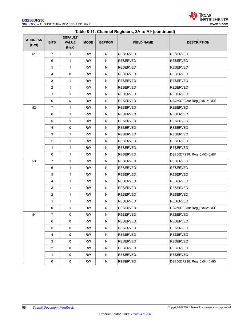
Table 8-11. Channel Registers, 3A to A9 (continued)
ADDRESS(Hex)
BITSDEFAULT
VALUE(Hex)
MODE EEPROM FIELD NAME DESCRIPTION
51 7 1 RW N RESERVED RESERVED
6 1 RW N RESERVED RESERVED
5 1 RW N RESERVED RESERVED
4 0 RW N RESERVED RESERVED
3 1 RW N RESERVED RESERVED
2 1 RW N RESERVED RESERVED
1 1 RW N RESERVED RESERVED
0 0 RW N RESERVED DS250DF230: Reg_0x51=0xEE
52 7 1 RW N RESERVED RESERVED
6 1 RW N RESERVED RESERVED
5 1 RW N RESERVED RESERVED
4 0 RW N RESERVED RESERVED
3 1 RW N RESERVED RESERVED
2 1 RW N RESERVED RESERVED
1 1 RW N RESERVED RESERVED
0 1 RW N RESERVED DS250DF230: Reg_0x52=0xEF
53 7 1 RW N RESERVED RESERVED
6 1 RW N RESERVED RESERVED
5 1 RW N RESERVED RESERVED
4 1 RW N RESERVED RESERVED
3 1 RW N RESERVED RESERVED
2 1 RW N RESERVED RESERVED
1 1 RW N RESERVED RESERVED
0 1 RW N RESERVED DS250DF230: Reg_0x53=0xFF
54 7 0 RW N RESERVED RESERVED
6 0 RW N RESERVED RESERVED
5 0 RW N RESERVED RESERVED
4 0 RW N RESERVED RESERVED
3 0 RW N RESERVED RESERVED
2 0 RW N RESERVED RESERVED
1 0 RW N RESERVED RESERVED
0 0 RW N RESERVED DS250DF230: Reg_0x54=0x00
DS250DF230SNLS590C – AUGUST 2018 – REVISED JUNE 2021 www.ti.com
68 Submit Document Feedback Copyright © 2021 Texas Instruments Incorporated
Product Folder Links: DS250DF230

Table 8-11. Channel Registers, 3A to A9 (continued)
ADDRESS(Hex)
BITSDEFAULT
VALUE(Hex)
MODE EEPROM FIELD NAME DESCRIPTION
55 7 0 RW N RESERVED RESERVED
6 0 RW N RESERVED RESERVED
5 0 RW N RESERVED RESERVED
4 0 RW N RESERVED RESERVED
3 0 RW N RESERVED RESERVED
2 0 RW N RESERVED RESERVED
1 0 RW N RESERVED RESERVED
0 0 RW N RESERVED DS250DF230: Reg_0x55=0x00
56 7 0 RW N RESERVED RESERVED
6 0 RW N RESERVED RESERVED
5 0 RW N RESERVED RESERVED
4 0 RW N RESERVED RESERVED
3 0 RW N RESERVED RESERVED
2 0 RW N RESERVED RESERVED
1 0 RW N RESERVED RESERVED
0 0 RW N RESERVED DS250DF230: Reg_0x56=0x00
57 7 0 RW N RESERVED RESERVED
6 0 RW N RESERVED RESERVED
5 0 RW N RESERVED RESERVED
4 0 RW N RESERVED RESERVED
3 0 RW N RESERVED RESERVED
2 0 RW N RESERVED RESERVED
1 0 RW N RESERVED RESERVED
0 0 RW N RESERVED DS250DF230: Reg_0x57=0x00
58 7 0 RW N RESERVED RESERVED
6 0 RW N RESERVED RESERVED
5 0 RW N RESERVED RESERVED
4 0 RW N RESERVED RESERVED
3 0 RW N RESERVED RESERVED
2 0 RW N RESERVED RESERVED
1 0 RW N RESERVED RESERVED
0 0 RW N RESERVED DS250DF230: Reg_0x58=0x00
www.ti.comDS250DF230
SNLS590C – AUGUST 2018 – REVISED JUNE 2021
Copyright © 2021 Texas Instruments Incorporated Submit Document Feedback 69
Product Folder Links: DS250DF230
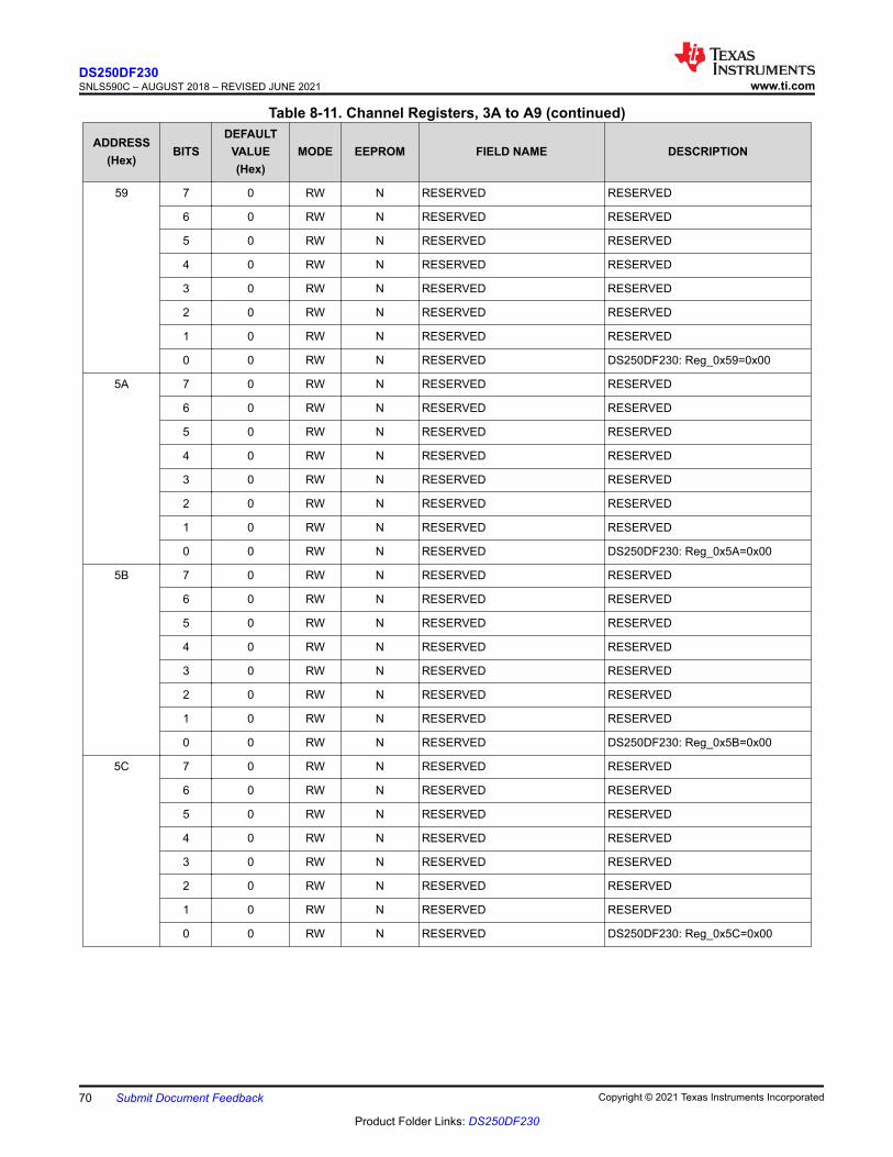
Table 8-11. Channel Registers, 3A to A9 (continued)
ADDRESS(Hex)
BITSDEFAULT
VALUE(Hex)
MODE EEPROM FIELD NAME DESCRIPTION
59 7 0 RW N RESERVED RESERVED
6 0 RW N RESERVED RESERVED
5 0 RW N RESERVED RESERVED
4 0 RW N RESERVED RESERVED
3 0 RW N RESERVED RESERVED
2 0 RW N RESERVED RESERVED
1 0 RW N RESERVED RESERVED
0 0 RW N RESERVED DS250DF230: Reg_0x59=0x00
5A 7 0 RW N RESERVED RESERVED
6 0 RW N RESERVED RESERVED
5 0 RW N RESERVED RESERVED
4 0 RW N RESERVED RESERVED
3 0 RW N RESERVED RESERVED
2 0 RW N RESERVED RESERVED
1 0 RW N RESERVED RESERVED
0 0 RW N RESERVED DS250DF230: Reg_0x5A=0x00
5B 7 0 RW N RESERVED RESERVED
6 0 RW N RESERVED RESERVED
5 0 RW N RESERVED RESERVED
4 0 RW N RESERVED RESERVED
3 0 RW N RESERVED RESERVED
2 0 RW N RESERVED RESERVED
1 0 RW N RESERVED RESERVED
0 0 RW N RESERVED DS250DF230: Reg_0x5B=0x00
5C 7 0 RW N RESERVED RESERVED
6 0 RW N RESERVED RESERVED
5 0 RW N RESERVED RESERVED
4 0 RW N RESERVED RESERVED
3 0 RW N RESERVED RESERVED
2 0 RW N RESERVED RESERVED
1 0 RW N RESERVED RESERVED
0 0 RW N RESERVED DS250DF230: Reg_0x5C=0x00
DS250DF230SNLS590C – AUGUST 2018 – REVISED JUNE 2021 www.ti.com
70 Submit Document Feedback Copyright © 2021 Texas Instruments Incorporated
Product Folder Links: DS250DF230

Table 8-11. Channel Registers, 3A to A9 (continued)
ADDRESS(Hex)
BITSDEFAULT
VALUE(Hex)
MODE EEPROM FIELD NAME DESCRIPTION
5D 7 0 RW N RESERVED RESERVED
6 0 RW N RESERVED RESERVED
5 0 RW N RESERVED RESERVED
4 0 RW N RESERVED RESERVED
3 0 RW N RESERVED RESERVED
2 0 RW N RESERVED RESERVED
1 0 RW N RESERVED RESERVED
0 0 RW N RESERVED DS250DF230: Reg_0x5D=0x00
5E 7 0 RW N RESERVED RESERVED
6 0 RW N RESERVED RESERVED
5 0 RW N RESERVED RESERVED
4 0 RW N RESERVED RESERVED
3 0 RW N RESERVED RESERVED
2 0 RW N RESERVED RESERVED
1 0 RW N RESERVED RESERVED
0 0 RW N RESERVED DS250DF230: Reg_0x5E=0x00
5F 7 0 RW N RESERVED RESERVED
6 0 RW N RESERVED RESERVED
5 0 RW N RESERVED RESERVED
4 0 RW N RESERVED RESERVED
3 0 RW N RESERVED RESERVED
2 0 RW N RESERVED RESERVED
1 0 RW N RESERVED RESERVED
0 0 RW N RESERVED DS250DF230: Reg_0x5F=0x00
60 7 0 RW Y GRP0_OV_CNT[7] Group 0 count LSB
6 0 RW Y GRP0_OV_CNT[6]
5 0 RW Y GRP0_OV_CNT[5]
4 0 RW Y GRP0_OV_CNT[4]
3 0 RW Y GRP0_OV_CNT[3]
2 0 RW Y GRP0_OV_CNT[2]
1 0 RW Y GRP0_OV_CNT[1]
0 0 RW Y GRP0_OV_CNT[0]
www.ti.comDS250DF230
SNLS590C – AUGUST 2018 – REVISED JUNE 2021
Copyright © 2021 Texas Instruments Incorporated Submit Document Feedback 71
Product Folder Links: DS250DF230

Table 8-11. Channel Registers, 3A to A9 (continued)
ADDRESS(Hex)
BITSDEFAULT
VALUE(Hex)
MODE EEPROM FIELD NAME DESCRIPTION
61 7 0 RW Y CNT_DLTA_OV_0 Override enable for group 0 manual data rate selection
6 0 RW Y GRP0_OV_CNT[14] Group 0 count MSB
5 0 RW Y GRP0_OV_CNT[13]
4 0 RW Y GRP0_OV_CNT[12]
3 0 RW Y GRP0_OV_CNT[11]
2 0 RW Y GRP0_OV_CNT[10]
1 0 RW Y GRP0_OV_CNT[9]
0 0 RW Y GRP0_OV_CNT[8]
62 7 0 RW Y GRP1_OV_CNT[7] Group 1 count LSB
6 0 RW Y GRP1_OV_CNT[6]
5 0 RW Y GRP1_OV_CNT[5]
4 0 RW Y GRP1_OV_CNT[4]
3 0 RW Y GRP1_OV_CNT[3]
2 0 RW Y GRP1_OV_CNT[2]
1 0 RW Y GRP1_OV_CNT[1]
0 0 RW Y GRP1_OV_CNT[0]
63 7 0 RW Y CNT_DLTA_OV_1 Override enable for group 1 manual data rate selection
6 0 RW Y GRP1_OV_CNT[14] Group 1 count MSB
5 0 RW Y GRP1_OV_CNT[13]
4 0 RW Y GRP1_OV_CNT[12]
3 0 RW Y GRP1_OV_CNT[11]
2 0 RW Y GRP1_OV_CNT[10]
1 0 RW Y GRP1_OV_CNT[9]
0 0 RW Y GRP1_OV_CNT[8]
64 7 0 RW Y GRP0_OV_DLTA[3] Sets the PPM delta tolerance for the PPM counter lock check for group 0. Must also program channel Reg_0x67[7].
6 0 RW Y GRP0_OV_DLTA[2]
5 0 RW Y GRP0_OV_DLTA[1]
4 0 RW Y GRP0_OV_DLTA[0]
3 0 RW Y GRP1_OV_DLTA[3] Sets the PPM delta tolerance for the PPM counter lock check for group 1. Must also program channel Reg_0x67[6].
2 0 RW Y GRP1_OV_DLTA[2]
1 0 RW Y GRP1_OV_DLTA[1]
0 0 RW Y GRP1_OV_DLTA[0]
DS250DF230SNLS590C – AUGUST 2018 – REVISED JUNE 2021 www.ti.com
72 Submit Document Feedback Copyright © 2021 Texas Instruments Incorporated
Product Folder Links: DS250DF230
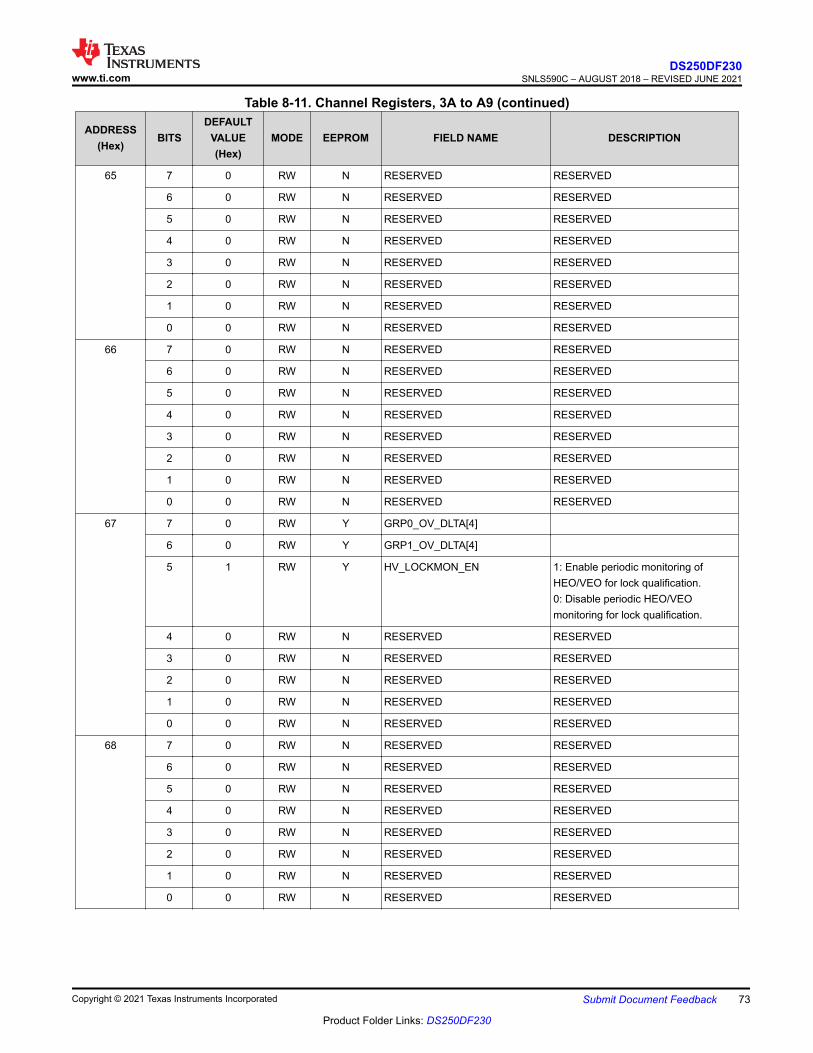
Table 8-11. Channel Registers, 3A to A9 (continued)
ADDRESS(Hex)
BITSDEFAULT
VALUE(Hex)
MODE EEPROM FIELD NAME DESCRIPTION
65 7 0 RW N RESERVED RESERVED
6 0 RW N RESERVED RESERVED
5 0 RW N RESERVED RESERVED
4 0 RW N RESERVED RESERVED
3 0 RW N RESERVED RESERVED
2 0 RW N RESERVED RESERVED
1 0 RW N RESERVED RESERVED
0 0 RW N RESERVED RESERVED
66 7 0 RW N RESERVED RESERVED
6 0 RW N RESERVED RESERVED
5 0 RW N RESERVED RESERVED
4 0 RW N RESERVED RESERVED
3 0 RW N RESERVED RESERVED
2 0 RW N RESERVED RESERVED
1 0 RW N RESERVED RESERVED
0 0 RW N RESERVED RESERVED
67 7 0 RW Y GRP0_OV_DLTA[4]
6 0 RW Y GRP1_OV_DLTA[4]
5 1 RW Y HV_LOCKMON_EN 1: Enable periodic monitoring of HEO/VEO for lock qualification.0: Disable periodic HEO/VEO monitoring for lock qualification.
4 0 RW N RESERVED RESERVED
3 0 RW N RESERVED RESERVED
2 0 RW N RESERVED RESERVED
1 0 RW N RESERVED RESERVED
0 0 RW N RESERVED RESERVED
68 7 0 RW N RESERVED RESERVED
6 0 RW N RESERVED RESERVED
5 0 RW N RESERVED RESERVED
4 0 RW N RESERVED RESERVED
3 0 RW N RESERVED RESERVED
2 0 RW N RESERVED RESERVED
1 0 RW N RESERVED RESERVED
0 0 RW N RESERVED RESERVED
www.ti.comDS250DF230
SNLS590C – AUGUST 2018 – REVISED JUNE 2021
Copyright © 2021 Texas Instruments Incorporated Submit Document Feedback 73
Product Folder Links: DS250DF230

Table 8-11. Channel Registers, 3A to A9 (continued)
ADDRESS(Hex)
BITSDEFAULT
VALUE(Hex)
MODE EEPROM FIELD NAME DESCRIPTION
69 7 0 RW N RESERVED RESERVED
6 0 RW N RESERVED RESERVED
5 0 RW N RESERVED RESERVED
4 0 RW N RESERVED RESERVED
3 1 RW Y RESERVED RESERVED
2 0 RW Y RESERVED RESERVED
1 1 RW Y RESERVED RESERVED
0 0 RW Y RESERVED RESERVED
6A 7 0 RW Y VEO_LCK_THRSH[3] VEO threshold to meet before lock is established. The LSB step size is 4 counts of VEO.
6 0 RW Y VEO_LCK_THRSH[2]
5 1 RW Y VEO_LCK_THRSH[1]
4 0 RW Y VEO_LCK_THRSH[0]
3 0 RW Y HEO_LCK_THRSH[3] HEO threshold to meet before lock is established. The LSB step size is 4 counts of HEO.
2 0 RW Y HEO_LCK_THRSH[2]
1 0 RW Y HEO_LCK_THRSH[1]
0 1 RW Y HEO_LCK_THRSH[0]
6B 7 0 RW Y RESERVED RESERVED
6 1 RW Y FOM_A[6] Alternate Figure of Merit variable A. Max value for this register is 128.5 0 RW Y FOM_A[5]
4 0 RW Y FOM_A[4]
3 0 RW Y FOM_A[3]
2 0 RW Y FOM_A[2]
1 0 RW Y FOM_A[1]
0 0 RW Y FOM_A[0]
6C 7 0 RW Y FOM_B[7] HEO adjustment for Alternate FoM, variable B6 0 RW Y FOM_B[6]
5 0 RW Y FOM_B[5]
4 0 RW Y FOM_B[4]
3 0 RW Y FOM_B[3]
2 0 RW Y FOM_B[2]
1 0 RW Y FOM_B[1]
0 0 RW Y FOM_B[0]
DS250DF230SNLS590C – AUGUST 2018 – REVISED JUNE 2021 www.ti.com
74 Submit Document Feedback Copyright © 2021 Texas Instruments Incorporated
Product Folder Links: DS250DF230

Table 8-11. Channel Registers, 3A to A9 (continued)
ADDRESS(Hex)
BITSDEFAULT
VALUE(Hex)
MODE EEPROM FIELD NAME DESCRIPTION
6D 7 0 RW Y FOM_C[7] VEO adjustment for Alternate FoM, variable C6 0 RW Y FOM_C[6]
5 0 RW Y FOM_C[5]
4 0 RW Y FOM_C[4]
3 0 RW Y FOM_C[3]
2 0 RW Y FOM_C[2]
1 0 RW Y FOM_C[1]
0 0 RW Y FOM_C[0]
6E 7 0 RW Y EN_NEW_FOM_CTLE 1: CTLE adaption state machine will use the alternate FoMHEO_ALT = (HEO-B)*A*2VEO_ALT = (VEO-C)*(1-A)*2The values of A,B,C are set in channel Reg_0x6B, 0x6C, and 0x6D.The value of A is equal to the register value divided by 128.The Alternate FoM = (HEOB)*A*2 + (VEO-C)*(1-A)*2
6 0 RW Y EN_NEW_FOM_DFE 1: DFE adaption state machine will use the alternate FoM.HEO_ALT = (HEO-B)*A*2VEO_ALT = (VEO-C)*(1-A)*2The values of A,B,C are set in channel Reg_0x6B, 0x6C, and 0x6D.The value of A is equal to the register value divided by 128The Alternate FoM = (HEOB)*A*2 + (VEO-C)*(1-A)*2
5 0 RW N RESERVED RESERVED
4 0 RW N RESERVED RESERVED
3 0 RW N RESERVED RESERVED
2 0 RW N RESERVED RESERVED
1 0 RW N RESERVED RESERVED
0 0 RW N RESERVED RESERVED
www.ti.comDS250DF230
SNLS590C – AUGUST 2018 – REVISED JUNE 2021
Copyright © 2021 Texas Instruments Incorporated Submit Document Feedback 75
Product Folder Links: DS250DF230
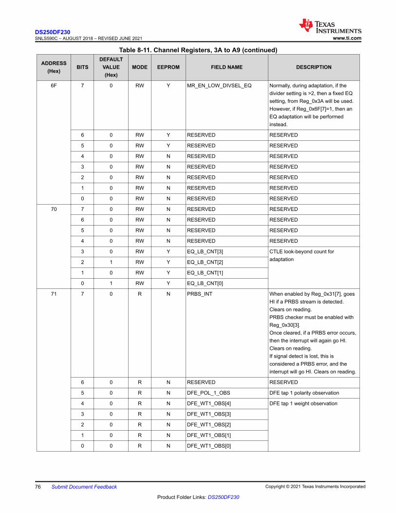
Table 8-11. Channel Registers, 3A to A9 (continued)
ADDRESS(Hex)
BITSDEFAULT
VALUE(Hex)
MODE EEPROM FIELD NAME DESCRIPTION
6F 7 0 RW Y MR_EN_LOW_DIVSEL_EQ Normally, during adaptation, if the divider setting is >2, then a fixed EQ setting, from Reg_0x3A will be used. However, if Reg_0x6F[7]=1, then an EQ adaptation will be performed instead.
6 0 RW Y RESERVED RESERVED
5 0 RW Y RESERVED RESERVED
4 0 RW N RESERVED RESERVED
3 0 RW N RESERVED RESERVED
2 0 RW N RESERVED RESERVED
1 0 RW N RESERVED RESERVED
0 0 RW N RESERVED RESERVED
70 7 0 RW N RESERVED RESERVED
6 0 RW N RESERVED RESERVED
5 0 RW N RESERVED RESERVED
4 0 RW N RESERVED RESERVED
3 0 RW Y EQ_LB_CNT[3] CTLE look-beyond count for adaptation2 1 RW Y EQ_LB_CNT[2]
1 0 RW Y EQ_LB_CNT[1]
0 1 RW Y EQ_LB_CNT[0]
71 7 0 R N PRBS_INT When enabled by Reg_0x31[7], goes HI if a PRBS stream is detected. Clears on reading.PRBS checker must be enabled with Reg_0x30[3].Once cleared, if a PRBS error occurs, then the interrupt will again go HI. Clears on reading.If signal detect is lost, this is considered a PRBS error, and the interrupt will go HI. Clears on reading.
6 0 R N RESERVED RESERVED
5 0 R N DFE_POL_1_OBS DFE tap 1 polarity observation
4 0 R N DFE_WT1_OBS[4] DFE tap 1 weight observation
3 0 R N DFE_WT1_OBS[3]
2 0 R N DFE_WT1_OBS[2]
1 0 R N DFE_WT1_OBS[1]
0 0 R N DFE_WT1_OBS[0]
DS250DF230SNLS590C – AUGUST 2018 – REVISED JUNE 2021 www.ti.com
76 Submit Document Feedback Copyright © 2021 Texas Instruments Incorporated
Product Folder Links: DS250DF230
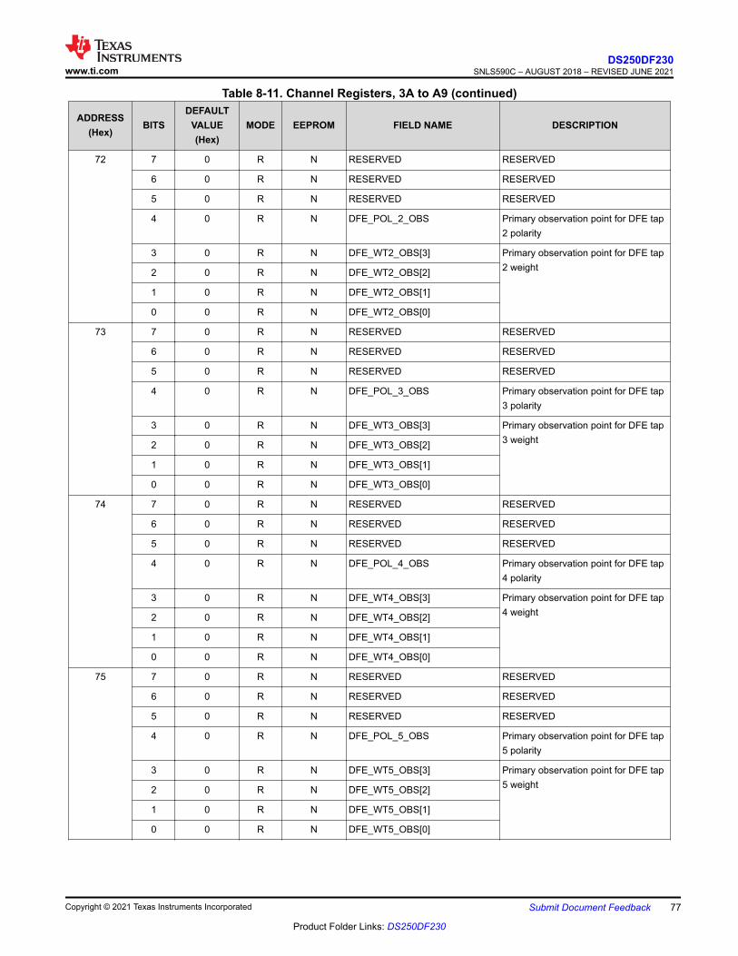
Table 8-11. Channel Registers, 3A to A9 (continued)
ADDRESS(Hex)
BITSDEFAULT
VALUE(Hex)
MODE EEPROM FIELD NAME DESCRIPTION
72 7 0 R N RESERVED RESERVED
6 0 R N RESERVED RESERVED
5 0 R N RESERVED RESERVED
4 0 R N DFE_POL_2_OBS Primary observation point for DFE tap 2 polarity
3 0 R N DFE_WT2_OBS[3] Primary observation point for DFE tap 2 weight2 0 R N DFE_WT2_OBS[2]
1 0 R N DFE_WT2_OBS[1]
0 0 R N DFE_WT2_OBS[0]
73 7 0 R N RESERVED RESERVED
6 0 R N RESERVED RESERVED
5 0 R N RESERVED RESERVED
4 0 R N DFE_POL_3_OBS Primary observation point for DFE tap 3 polarity
3 0 R N DFE_WT3_OBS[3] Primary observation point for DFE tap 3 weight2 0 R N DFE_WT3_OBS[2]
1 0 R N DFE_WT3_OBS[1]
0 0 R N DFE_WT3_OBS[0]
74 7 0 R N RESERVED RESERVED
6 0 R N RESERVED RESERVED
5 0 R N RESERVED RESERVED
4 0 R N DFE_POL_4_OBS Primary observation point for DFE tap 4 polarity
3 0 R N DFE_WT4_OBS[3] Primary observation point for DFE tap 4 weight2 0 R N DFE_WT4_OBS[2]
1 0 R N DFE_WT4_OBS[1]
0 0 R N DFE_WT4_OBS[0]
75 7 0 R N RESERVED RESERVED
6 0 R N RESERVED RESERVED
5 0 R N RESERVED RESERVED
4 0 R N DFE_POL_5_OBS Primary observation point for DFE tap 5 polarity
3 0 R N DFE_WT5_OBS[3] Primary observation point for DFE tap 5 weight2 0 R N DFE_WT5_OBS[2]
1 0 R N DFE_WT5_OBS[1]
0 0 R N DFE_WT5_OBS[0]
www.ti.comDS250DF230
SNLS590C – AUGUST 2018 – REVISED JUNE 2021
Copyright © 2021 Texas Instruments Incorporated Submit Document Feedback 77
Product Folder Links: DS250DF230

Table 8-11. Channel Registers, 3A to A9 (continued)
ADDRESS(Hex)
BITSDEFAULT
VALUE(Hex)
MODE EEPROM FIELD NAME DESCRIPTION
76 7 0 RW Y POST_LOCK_VEO_THR[3] VEO threshold after LOCK is established6 0 RW Y POST_LOCK_VEO_THR[2]
5 1 RW Y POST_LOCK_VEO_THR[1]
4 0 RW Y POST_LOCK_VEO_THR[0]
3 0 RW Y POST_LOCK_HEO_THR[3] HEO threshold after LOCK is established2 0 RW Y POST_LOCK_HEO_THR[2]
1 0 RW Y POST_LOCK_HEO_THR[1]
0 1 RW Y POST_LOCK_HEO_THR[0]
77 7 0 RW N PRBS_GEN_POL_EN 1: Force polarity inversion on generated PRBS data
6 0 RW Y RESERVED RESERVED
5 0 RW Y RESERVED RESERVED
4 1 RW Y RESERVED RESERVED
3 1 RW Y RESERVED RESERVED
2 0 RW Y RESERVED RESERVED
1 1 RW Y RESERVED RESERVED
0 0 RW N RESERVED RESERVED
DS250DF230SNLS590C – AUGUST 2018 – REVISED JUNE 2021 www.ti.com
78 Submit Document Feedback Copyright © 2021 Texas Instruments Incorporated
Product Folder Links: DS250DF230

Table 8-11. Channel Registers, 3A to A9 (continued)
ADDRESS(Hex)
BITSDEFAULT
VALUE(Hex)
MODE EEPROM FIELD NAME DESCRIPTION
78 7 0 R N RESERVED RESERVED
6 0 R N RESERVED RESERVED
5 0 R N SD_STATUS Primary observation point for signal detect status
4 0 R N CDR_LOCK_STATUS Primary observation point for CDR lock status
3 0 R N CDR_LOCK_INT Requires that channel Reg_0x79[1] be set.1: Indicates CDR has achieved lock, lock goes from LOW to HIGH. This bit is cleared after reading. This bit will stay set until it has been cleared by reading.
2 0 R N SD_INT Requires that channel Reg_0x79[0] be set.1: Indicates signal detect status has changed. This will trigger when signal detect goes from LOW to HIGH or HIGH to LOW. This bit is cleared after reading. This bit will stay set until it has been cleared by reading.
1 0 R N EOM_VRANGE_LIMIT_ERROR Goes high if GET_HEO_VEO indicates high during adaptation
0 0 R N HEO_VEO_INT Requires that channel Reg_0x36[6] be set.1: Indicates that HEO/VEO dropped below the limits set in channel Reg_0x76 This bit is cleared after reading. This bit will stay set until it has been cleared by reading.
79 7 0 RW N RESERVED RESERVED
6 0 RW N PRBS_CHKR_EN 1: Enable the PRBS checker.0: Disable the PRBS checker
5 0 RW N PRBS_GEN_EN 1: Enable the pattern generator0: Disable the pattern generator
4 1 RW N RESERVED RESERVED
3 0 RW N RESERVED RESERVED
2 0 RW N RESERVED RESERVED
1 0 RW Y CDR_LOCK_INT_EN 1: Enable CDR lock interrupt, observable in channel Reg_0x78[3]0: Disable CDR lock interrupt
0 0 RW Y SD_INT_EN 1: Enable signal detect interrupt, observable in channel Reg_0x78[3]0: Disable signal detect interrupt
www.ti.comDS250DF230
SNLS590C – AUGUST 2018 – REVISED JUNE 2021
Copyright © 2021 Texas Instruments Incorporated Submit Document Feedback 79
Product Folder Links: DS250DF230
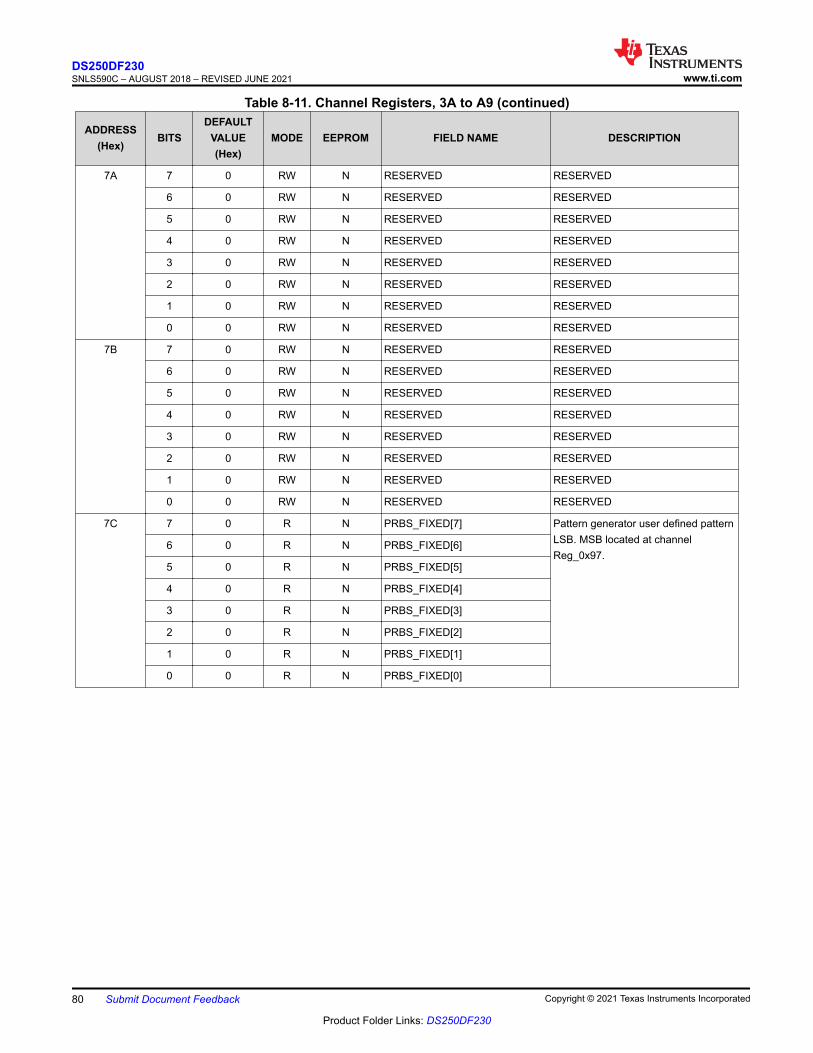
Table 8-11. Channel Registers, 3A to A9 (continued)
ADDRESS(Hex)
BITSDEFAULT
VALUE(Hex)
MODE EEPROM FIELD NAME DESCRIPTION
7A 7 0 RW N RESERVED RESERVED
6 0 RW N RESERVED RESERVED
5 0 RW N RESERVED RESERVED
4 0 RW N RESERVED RESERVED
3 0 RW N RESERVED RESERVED
2 0 RW N RESERVED RESERVED
1 0 RW N RESERVED RESERVED
0 0 RW N RESERVED RESERVED
7B 7 0 RW N RESERVED RESERVED
6 0 RW N RESERVED RESERVED
5 0 RW N RESERVED RESERVED
4 0 RW N RESERVED RESERVED
3 0 RW N RESERVED RESERVED
2 0 RW N RESERVED RESERVED
1 0 RW N RESERVED RESERVED
0 0 RW N RESERVED RESERVED
7C 7 0 R N PRBS_FIXED[7] Pattern generator user defined pattern LSB. MSB located at channel Reg_0x97.
6 0 R N PRBS_FIXED[6]
5 0 R N PRBS_FIXED[5]
4 0 R N PRBS_FIXED[4]
3 0 R N PRBS_FIXED[3]
2 0 R N PRBS_FIXED[2]
1 0 R N PRBS_FIXED[1]
0 0 R N PRBS_FIXED[0]
DS250DF230SNLS590C – AUGUST 2018 – REVISED JUNE 2021 www.ti.com
80 Submit Document Feedback Copyright © 2021 Texas Instruments Incorporated
Product Folder Links: DS250DF230

Table 8-11. Channel Registers, 3A to A9 (continued)
ADDRESS(Hex)
BITSDEFAULT
VALUE(Hex)
MODE EEPROM FIELD NAME DESCRIPTION
7D 7 0 RW Y CONT_ADAPT_HEO_CHNG_THRS[3]
Limit for HEO change before triggering a DFE adaption while continuous DFE adaption is enabled.6 1 RW Y CONT_ADAPT_HEO_CHNG_TH
RS[2]
5 0 RW Y CONT_ADAPT_HEO_CHNG_THRS[1]
4 0 RW Y CONT_ADAPT_HEO_CHNG_THRS[0]
3 1 RW Y CONT_ADAPT_VEO_CHNG_THRS[3]
Limit for VEO change before triggering a DFE adaption while continuous DFE adaption is enabled.(Refer to the Programming Guide for more details)
2 0 RW Y CONT_ADAPT_VEO_CHNG_THRS[2]
1 0 RW Y CONT_ADAPT_VEO_CHNG_THRS[1]
0 0 RW Y CONT_ADAPT_VEO_CHNG_THRS[0]
7E 7 0 RW Y CONT_ADPT_TAP_INCR[3] Limit for allowable tap increase from the previous base point6 0 RW Y CONT_ADPT_TAP_INCR[2]
5 0 RW Y CONT_ADPT_TAP_INCR[1]
4 1 RW Y CONT_ADPT_TAP_INCR[0]
3 0 RW Y RESERVED RESERVED
2 0 RW Y RESERVED RESERVED
1 1 RW Y RESERVED RESERVED
0 1 RW Y RESERVED RESERVED
www.ti.comDS250DF230
SNLS590C – AUGUST 2018 – REVISED JUNE 2021
Copyright © 2021 Texas Instruments Incorporated Submit Document Feedback 81
Product Folder Links: DS250DF230

Table 8-11. Channel Registers, 3A to A9 (continued)
ADDRESS(Hex)
BITSDEFAULT
VALUE(Hex)
MODE EEPROM FIELD NAME DESCRIPTION
7F 7 0 RW N EN_OBS_ALT_FOM 1: Allows for alternate FoM calculation to be shown in channel registers Reg_0x27, Reg_0x28 and Reg_0x29 instead of HEO and VEO
6 0 RW N RESERVED RESERVED
5 1 RW Y RESERVED RESERVED
4 0 RW Y EN_DFE_CONT_ADAPT 1: Continuous DFE adaption is enabled0: DFE adapts only during lock and then freezes(Refer to the Programming Guide for more details)
3 1 RW Y CONT_ADPT_CMP_BOTH 1: If continuous DFE adaption is enabled, a DFE adaption will trigger if either HEO orVEO degrades
2 0 RW Y CONT_ADPT_COUNT[2] Limit for number of weights the DFE can look ahead in continuous adaption.(Refer to the Programming Guide for more details)
1 1 RW Y CONT_ADPT_COUNT[1]
0 0 RW Y CONT_ADPT_COUNT[0]
80 7 0 R N RESERVED RESERVED
6 0 R N RESERVED RESERVED
5 0 R N RESERVED RESERVED
4 0 R N RESERVED RESERVED
3 0 R N RESERVED RESERVED
2 0 R N RESERVED RESERVED
1 0 R N RESERVED RESERVED
0 0 R N RESERVED RESERVED
81 7 1 R N RESERVED RESERVED
6 1 R N RESERVED RESERVED
5 1 R N RESERVED RESERVED
4 0 R N RESERVED RESERVED
3 0 R N RESERVED RESERVED
2 1 R N RESERVED RESERVED
1 0 R N RESERVED RESERVED
0 0 R N RESERVED RESERVED
DS250DF230SNLS590C – AUGUST 2018 – REVISED JUNE 2021 www.ti.com
82 Submit Document Feedback Copyright © 2021 Texas Instruments Incorporated
Product Folder Links: DS250DF230
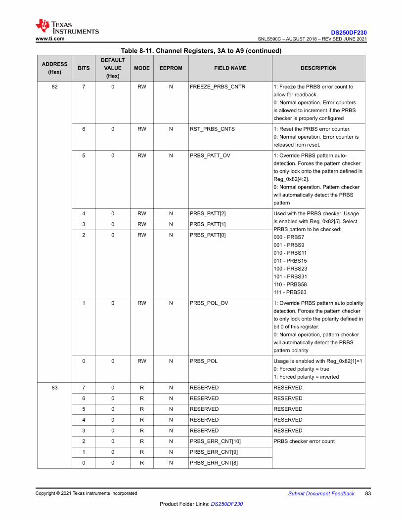
Table 8-11. Channel Registers, 3A to A9 (continued)
ADDRESS(Hex)
BITSDEFAULT
VALUE(Hex)
MODE EEPROM FIELD NAME DESCRIPTION
82 7 0 RW N FREEZE_PRBS_CNTR 1: Freeze the PRBS error count to allow for readback.0: Normal operation. Error counters is allowed to increment if the PRBS checker is properly configured
6 0 RW N RST_PRBS_CNTS 1: Reset the PRBS error counter.0: Normal operation. Error counter is released from reset.
5 0 RW N PRBS_PATT_OV 1: Override PRBS pattern auto-detection. Forces the pattern checker to only lock onto the pattern defined in Reg_0x82[4:2].0: Normal operation. Pattern checker will automatically detect the PRBS pattern
4 0 RW N PRBS_PATT[2] Used with the PRBS checker. Usage is enabled with Reg_0x82[5]. Select PRBS pattern to be checked:000 - PRBS7001 - PRBS9010 - PRBS11011 - PRBS15100 - PRBS23101 - PRBS31110 - PRBS58111 - PRBS63
3 0 RW N PRBS_PATT[1]
2 0 RW N PRBS_PATT[0]
1 0 RW N PRBS_POL_OV 1: Override PRBS pattern auto polarity detection. Forces the pattern checker to only lock onto the polarity defined in bit 0 of this register.0: Normal operation, pattern checker will automatically detect the PRBS pattern polarity
0 0 RW N PRBS_POL Usage is enabled with Reg_0x82[1]=10: Forced polarity = true1: Forced polarity = inverted
83 7 0 R N RESERVED RESERVED
6 0 R N RESERVED RESERVED
5 0 R N RESERVED RESERVED
4 0 R N RESERVED RESERVED
3 0 R N RESERVED RESERVED
2 0 R N PRBS_ERR_CNT[10] PRBS checker error count
1 0 R N PRBS_ERR_CNT[9]
0 0 R N PRBS_ERR_CNT[8]
www.ti.comDS250DF230
SNLS590C – AUGUST 2018 – REVISED JUNE 2021
Copyright © 2021 Texas Instruments Incorporated Submit Document Feedback 83
Product Folder Links: DS250DF230
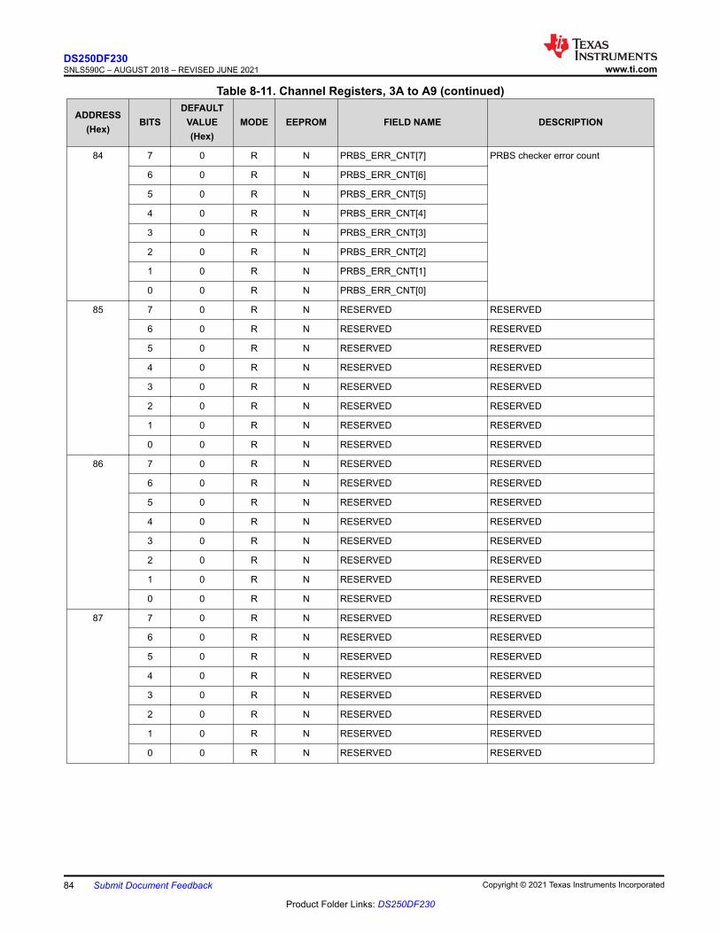
Table 8-11. Channel Registers, 3A to A9 (continued)
ADDRESS(Hex)
BITSDEFAULT
VALUE(Hex)
MODE EEPROM FIELD NAME DESCRIPTION
84 7 0 R N PRBS_ERR_CNT[7] PRBS checker error count
6 0 R N PRBS_ERR_CNT[6]
5 0 R N PRBS_ERR_CNT[5]
4 0 R N PRBS_ERR_CNT[4]
3 0 R N PRBS_ERR_CNT[3]
2 0 R N PRBS_ERR_CNT[2]
1 0 R N PRBS_ERR_CNT[1]
0 0 R N PRBS_ERR_CNT[0]
85 7 0 R N RESERVED RESERVED
6 0 R N RESERVED RESERVED
5 0 R N RESERVED RESERVED
4 0 R N RESERVED RESERVED
3 0 R N RESERVED RESERVED
2 0 R N RESERVED RESERVED
1 0 R N RESERVED RESERVED
0 0 R N RESERVED RESERVED
86 7 0 R N RESERVED RESERVED
6 0 R N RESERVED RESERVED
5 0 R N RESERVED RESERVED
4 0 R N RESERVED RESERVED
3 0 R N RESERVED RESERVED
2 0 R N RESERVED RESERVED
1 0 R N RESERVED RESERVED
0 0 R N RESERVED RESERVED
87 7 0 R N RESERVED RESERVED
6 0 R N RESERVED RESERVED
5 0 R N RESERVED RESERVED
4 0 R N RESERVED RESERVED
3 0 R N RESERVED RESERVED
2 0 R N RESERVED RESERVED
1 0 R N RESERVED RESERVED
0 0 R N RESERVED RESERVED
DS250DF230SNLS590C – AUGUST 2018 – REVISED JUNE 2021 www.ti.com
84 Submit Document Feedback Copyright © 2021 Texas Instruments Incorporated
Product Folder Links: DS250DF230

Table 8-11. Channel Registers, 3A to A9 (continued)
ADDRESS(Hex)
BITSDEFAULT
VALUE(Hex)
MODE EEPROM FIELD NAME DESCRIPTION
88 7 0 R N RESERVED RESERVED
6 0 R N RESERVED RESERVED
5 0 R N RESERVED RESERVED
4 0 R N RESERVED RESERVED
3 0 R N RESERVED RESERVED
2 0 R N RESERVED RESERVED
1 0 R N RESERVED RESERVED
0 0 R N RESERVED RESERVED
89 7 0 R N RESERVED RESERVED
6 0 R N RESERVED RESERVED
5 0 R N RESERVED RESERVED
4 0 R N RESERVED RESERVED
3 0 R N RESERVED RESERVED
2 0 R N RESERVED RESERVED
1 0 R N RESERVED RESERVED
0 0 R N RESERVED RESERVED
8A 7 0 R N RESERVED RESERVED
6 0 R N RESERVED RESERVED
5 0 R N RESERVED RESERVED
4 0 R N RESERVED RESERVED
3 0 R N RESERVED RESERVED
2 0 R N RESERVED RESERVED
1 0 R N RESERVED RESERVED
0 0 R N RESERVED RESERVED
8B 7 0 RW N RESERVED RESERVED
6 0 RW N RESERVED RESERVED
5 0 RW N RESERVED RESERVED
4 0 RW N RESERVED RESERVED
3 0 RW N RESERVED RESERVED
2 0 RW N RESERVED RESERVED
1 0 RW N RESERVED RESERVED
0 0 RW N RESERVED RESERVED
www.ti.comDS250DF230
SNLS590C – AUGUST 2018 – REVISED JUNE 2021
Copyright © 2021 Texas Instruments Incorporated Submit Document Feedback 85
Product Folder Links: DS250DF230

Table 8-11. Channel Registers, 3A to A9 (continued)
ADDRESS(Hex)
BITSDEFAULT
VALUE(Hex)
MODE EEPROM FIELD NAME DESCRIPTION
8C 7 0 RW N RESERVED RESERVED
6 0 RW N RESERVED RESERVED
5 0 RW N RESERVED RESERVED
4 0 RW N RESERVED RESERVED
3 0 RW N RESERVED RESERVED
2 0 RW N RESERVED RESERVED
1 0 RW N RESERVED RESERVED
0 0 RW N RESERVED RESERVED
8D 7 0 RW N RESERVED RESERVED
6 0 RW N RESERVED RESERVED
5 0 RW N RESERVED RESERVED
4 0 RW N RESERVED RESERVED
3 0 RW N RESERVED RESERVED
2 0 RW N RESERVED DS250DF230: RESERVED, 0
1 1 RW N RESERVED RESERVED
0 0 RW N RESERVED RESERVED
8E 7 0 RW N RESERVED RESERVED
6 0 RW N RESERVED RESERVED
5 0 RW N RESERVED RESERVED
4 0 RW N RESERVED RESERVED
3 0 RW N RESERVED RESERVED
2 0 RW N RESERVED RESERVED
1 0 RW N RESERVED RESERVED
0 0 RW Y VGA_SEL_GAIN VGA selection bit :1: VGA high-gain mode0: VGA low-gain mode(Refer to the Programming Guide for more details)
8F 7 0 R N EQ_BST_TO_EQ[7] Primary observation point for the EQ boost setting.6 0 R N EQ_BST_TO_EQ[6]
5 0 R N EQ_BST_TO_EQ5]
4 0 R N EQ_BST_TO_EQ[4]
3 0 R N EQ_BST_TO_EQ[3]
2 0 R N EQ_BST_TO_EQ[2]
1 0 R N EQ_BST_TO_EQ[1]
0 0 R N EQ_BST_TO_EQ[0]
DS250DF230SNLS590C – AUGUST 2018 – REVISED JUNE 2021 www.ti.com
86 Submit Document Feedback Copyright © 2021 Texas Instruments Incorporated
Product Folder Links: DS250DF230

Table 8-11. Channel Registers, 3A to A9 (continued)
ADDRESS(Hex)
BITSDEFAULT
VALUE(Hex)
MODE EEPROM FIELD NAME DESCRIPTION
90 7 0 RW N RESERVED RESERVED
6 0 RW N RESERVED RESERVED
5 0 RW N RESERVED RESERVED
4 0 RW N RESERVED RESERVED
3 0 RW N RESERVED RESERVED
2 0 RW N RESERVED RESERVED
1 0 RW N RESERVED RESERVED
0 0 RW N RESERVED RESERVED
91 7 0 RW N RESERVED RESERVED
6 0 RW N RESERVED RESERVED
5 0 RW N RESERVED RESERVED
4 0 RW N RESERVED RESERVED
3 0 RW N RESERVED RESERVED
2 0 RW N RESERVED RESERVED
1 0 RW N RESERVED RESERVED
0 0 RW N RESERVED RESERVED
92 7:0 0 RW N RESERVED RESERVED
93 7:0 0 RW N RESERVED RESERVED
94 7:0 0 RW N RESERVED RESERVED
95 ` 0 RW N SD_ENABLE 1: Force enable signal detect0: Normal operation
6 0 RW N SD_DISABLE 1: Force disable signal detect0: Normal operation
5 0 RW N DC_OFF_ENABLE 1: Force enable DC offset compensation0: Normal operation
4 0 RW N DC_OFF_DISABLE 1: Force disable DC offset compensation0: Normal operation
3 0 RW N EQ_ENABLE DS250DF230: 01: Force enable the CTLE0: Normal operation
2 0 RW N EQ_DISABLE 1: Force disable the CTLE0: Normal operation
1 0 RW N RESERVED RESERVED
0 0 RW N RESERVED RESERVED
www.ti.comDS250DF230
SNLS590C – AUGUST 2018 – REVISED JUNE 2021
Copyright © 2021 Texas Instruments Incorporated Submit Document Feedback 87
Product Folder Links: DS250DF230
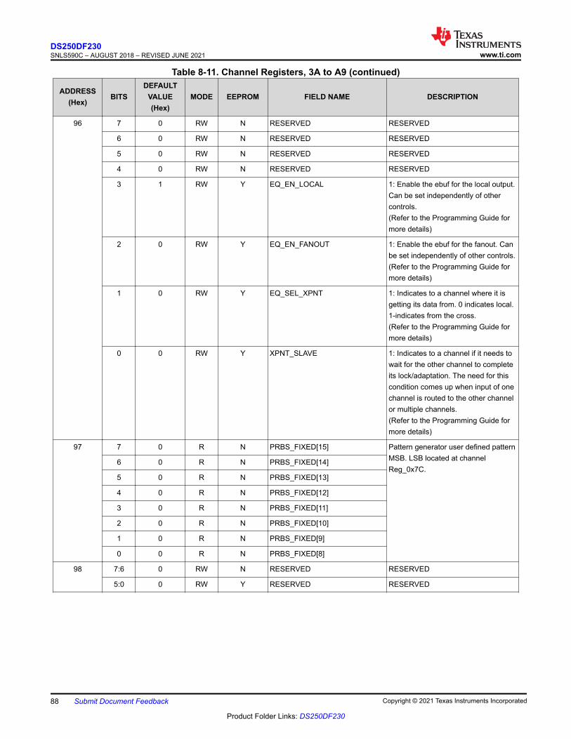
Table 8-11. Channel Registers, 3A to A9 (continued)
ADDRESS(Hex)
BITSDEFAULT
VALUE(Hex)
MODE EEPROM FIELD NAME DESCRIPTION
96 7 0 RW N RESERVED RESERVED
6 0 RW N RESERVED RESERVED
5 0 RW N RESERVED RESERVED
4 0 RW N RESERVED RESERVED
3 1 RW Y EQ_EN_LOCAL 1: Enable the ebuf for the local output. Can be set independently of other controls.(Refer to the Programming Guide for more details)
2 0 RW Y EQ_EN_FANOUT 1: Enable the ebuf for the fanout. Can be set independently of other controls.(Refer to the Programming Guide for more details)
1 0 RW Y EQ_SEL_XPNT 1: Indicates to a channel where it is getting its data from. 0 indicates local. 1-indicates from the cross.(Refer to the Programming Guide for more details)
0 0 RW Y XPNT_SLAVE 1: Indicates to a channel if it needs to wait for the other channel to complete its lock/adaptation. The need for this condition comes up when input of one channel is routed to the other channel or multiple channels.(Refer to the Programming Guide for more details)
97 7 0 R N PRBS_FIXED[15] Pattern generator user defined pattern MSB. LSB located at channel Reg_0x7C.
6 0 R N PRBS_FIXED[14]
5 0 R N PRBS_FIXED[13]
4 0 R N PRBS_FIXED[12]
3 0 R N PRBS_FIXED[11]
2 0 R N PRBS_FIXED[10]
1 0 R N PRBS_FIXED[9]
0 0 R N PRBS_FIXED[8]
98 7:6 0 RW N RESERVED RESERVED
5:0 0 RW Y RESERVED RESERVED
DS250DF230SNLS590C – AUGUST 2018 – REVISED JUNE 2021 www.ti.com
88 Submit Document Feedback Copyright © 2021 Texas Instruments Incorporated
Product Folder Links: DS250DF230

Table 8-11. Channel Registers, 3A to A9 (continued)
ADDRESS(Hex)
BITSDEFAULT
VALUE(Hex)
MODE EEPROM FIELD NAME DESCRIPTION
99 7 0 RW Y RESERVED RESERVED
6 0 RW Y RESERVED RESERVED
5 1 RW Y RESERVED RESERVED
4 1 RW Y RESERVED RESERVED
3 1 RW Y RESERVED RESERVED
2 1 RW Y RESERVED RESERVED
1 1 RW Y RESERVED RESERVED
0 1 RW Y RESERVED RESERVED
9A 7 0 RW Y RESERVED RESERVED
6 0 RW Y RESERVED RESERVED
5 1 RW Y RESERVED RESERVED
4 1 RW Y RESERVED RESERVED
3 1 RW Y RESERVED RESERVED
2 1 RW Y RESERVED RESERVED
1 1 RW Y RESERVED RESERVED
0 1 RW Y RESERVED RESERVED
9B 7 1 RW Y RESERVED RESERVED
6 1 RW Y RESERVED RESERVED
5 1 RW Y RESERVED RESERVED
4 0 RW Y RESERVED RESERVED
3 0 RW Y RESERVED RESERVED
2 0 RW Y RESERVED RESERVED
1 0 RW N RESERVED RESERVED
0 0 RW N RESERVED RESERVED
9C 7 0 RW N RESERVED RESERVED
6 0 RW N RESERVED RESERVED
5 1 RW Y RESERVED RESERVED
4 0 RW Y RESERVED RESERVED
3 0 RW Y RESERVED RESERVED
2 1 RW Y RESERVED RESERVED
1 0 RW Y RESERVED RESERVED
0 0 RW Y RESERVED RESERVED
www.ti.comDS250DF230
SNLS590C – AUGUST 2018 – REVISED JUNE 2021
Copyright © 2021 Texas Instruments Incorporated Submit Document Feedback 89
Product Folder Links: DS250DF230
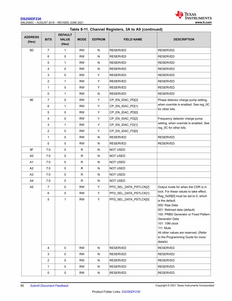
Table 8-11. Channel Registers, 3A to A9 (continued)
ADDRESS(Hex)
BITSDEFAULT
VALUE(Hex)
MODE EEPROM FIELD NAME DESCRIPTION
9D 7 1 RW N RESERVED RESERVED
6 0 RW N RESERVED RESERVED
5 1 RW N RESERVED RESERVED
4 0 RW N RESERVED RESERVED
3 0 RW Y RESERVED RESERVED
2 1 RW Y RESERVED RESERVED
1 0 RW Y RESERVED RESERVED
0 1 RW N RESERVED RESERVED
9E 7 0 RW Y CP_EN_IDAC_PD[2] Phase detector charge pump setting, when override is enabled. See reg_0C for other bits.
6 1 RW Y CP_EN_IDAC_PD[1]
5 0 RW Y CP_EN_IDAC_PD[0]
4 0 RW Y CP_EN_IDAC_FD[2] Frequency detector charge pump setting, when override is enabled. See reg_0C for other bits.
3 1 RW Y CP_EN_IDAC_FD[1]
2 0 RW Y CP_EN_IDAC_FD[0]
1 0 RW N RESERVED RESERVED
0 0 RW N RESERVED RESERVED
9F 7:0 0 R N NOT USED
A0 7:0 0 R N NOT USED
A1 7:0 0 R N NOT USED
A2 7:0 0 R N NOT USED
A3 7:0 0 R N NOT USED
A4 7:0 0 R N NOT USED
A5 7 0 RW Y PFD_SEL_DATA_PSTLCK[2] Output mode for when the CDR is in lock. For these values to take effect, Reg_0x09[5] must be set to 0, which is the default.000: Raw Data001: Retimed data (default)100: PRBS Generator or Fixed Pattern Generator Data101: 10M clock111: MuteAll other values are reserved. (Refer to the Programming Guide for more details)
6 0 RW Y PFD_SEL_DATA_PSTLCK[1]
5 1 RW Y PFD_SEL_DATA_PSTLCK[0]
4 0 RW N RESERVED RESERVED
3 0 RW N RESERVED RESERVED
2 0 RW N RESERVED RESERVED
1 0 RW N RESERVED RESERVED
0 0 RW N RESERVED RESERVED
DS250DF230SNLS590C – AUGUST 2018 – REVISED JUNE 2021 www.ti.com
90 Submit Document Feedback Copyright © 2021 Texas Instruments Incorporated
Product Folder Links: DS250DF230

Table 8-11. Channel Registers, 3A to A9 (continued)
ADDRESS(Hex)
BITSDEFAULT
VALUE(Hex)
MODE EEPROM FIELD NAME DESCRIPTION
A6 7 0 RW N INCR_HIST_TMR Provides an option to increase EOM timer given by 0x2A[7:4] for histogram collection by +8 for selection values < 8
6 1 RW Y EOM_TMR_ABRT_ON_HIT Enables faster scan through the eye-matrix by moving on to the next matrix point as soon as hit is observedNote: This bit does not affect when slope measurement are in progress
5 0 RW Y SLP_MIN_REQ_HITS[1] Minimum required hit count for registering a hit during slope measurements.
4 0 RW Y SLP_MIN_REQ_HITS[0]
3 0 RW Y LFT_SLP 0: allows slope measurement for the right side of the eye1: allows slope measurement for the left side of the eye
2 0 RW Y TOP_SLP 0: allows slope measurement for the bottom side of the eye1: allows slope measurement for the top side of the eye
1 1 RW Y DFE_BATHTUB_FOM Enables slope-based bathtub FoM for DFE adaptation
0 1 RW Y CTLE_BATHTUB_FOM Enables slope-based bathtub FoM for CTLE adaptation
A7 7:0 0 R N RESERVED RESERVED
A8 7:0 0 RW N RESERVED RESERVED
A9 7:0 0 RW Y RESERVED RESERVED
AC(DS250DF23
0 Only)
7 0 RW N MR_DIS_PRELCK_HV Disable heo veo acquisiton before lock
6 1 RW N MR_LPF_SAR_ADJST_EN Enables the use of temperature dependent LPF for Fastcap search
5 0 RW N RESERVED RESERVED
4 1 RW N RESERVED RESERVED
3 0 RW N MR_CPRI_CLK_DIV_SEL_OV clk divider enable for select, rclk_sel_div_lv
2 1 RW N MR_VCO_TLR_EN Enable the Cap extension of the VCO for TLR
1 0 RW N RESERVED RESERVED
0 0 RW N RESERVED RESERVED
www.ti.comDS250DF230
SNLS590C – AUGUST 2018 – REVISED JUNE 2021
Copyright © 2021 Texas Instruments Incorporated Submit Document Feedback 91
Product Folder Links: DS250DF230

9 Application and ImplementationNote
Information in the following applications sections is not part of the TI component specification, and TI does not warrant its accuracy or completeness. TI’s customers are responsible for determining suitability of components for their purposes, as well as validating and testing their design implementation to confirm system functionality.
9.1 Application InformationThe DS250DF230 is a high-speed retimer which extends the reach of differential channels and cleans jitter and other signal impairments in the process. It can be deployed in a variety of different systems from backplanes to front ports to active cable assemblies. The following sections outline a few typical applications and their associated design considerations.
9.2 Typical ApplicationsThe DS250DF230 is typically used in the following application scenarios:1. Front-Port Jitter Cleaning Applications2. Active Cable Applications3. Backplane and Mid-Plane Applications
Line Card
Switch Fabric
ASIC
FPGA
DS
25
0D
F2
30
DS
25
0D
F2
30
Co
nn
ecto
r
ASIC
FPGA
DS250DF230
Optical
25G-LR
x4
25G-LR
Active Copper
x4 25G
DS250DF230
DS250DF230
DS250DF230
x4
25G-VSR
x4
QSFP28
SFP28/QSFP28
x4
25G-LR
Figure 9-1. Typical Uses for the DS250DF230 in a System
DS250DF230SNLS590C – AUGUST 2018 – REVISED JUNE 2021 www.ti.com
92 Submit Document Feedback Copyright © 2021 Texas Instruments Incorporated
Product Folder Links: DS250DF230
9.2.1 Front-Port Jitter Cleaning Applications
The DS250DF230 has strong equalization capabilities that allow it to equalize insertion loss, reduce jitter, and extend the reach of front-port interfaces. Two pieces DS250DF230 can be used to support all four egress channels for a 100GbE port. Another two pieces DS250DF230 can be used to support all four ingress channels for the same 100GbE ports. Alternatively, a single DS250DF230 can be used to support all egress channels for two 25GbE ports, and another DS250DF230 can be used to support all two ingress channels for the same four 25GbE ports.
A flow-through pinout for the high-speed signals on DS250DF230 makes placement and routing easy for unidirectional application. By using the 2x2 cross point inside the device, DS250DF230 can also be configured for Figure 9-2, where one single device supports both egress and ingress channels.
ASIC
FPGA
RX0
RX1
TX0
TX1
TD
RD
DS250DF230 SFP28
Figure 9-2. Bidirectional Application
For applications which require IEEE802.3 100GBASE-CR4 or 25GBASE-CR auto-negotiation and link training, a linear repeater device such as the DS280BR820 (or similar) is recommended.
Figure 9-3 shows this configuration, and Figure 9-4 shows an example simplified schematic for a typical front-port application.
Network Interface Card (NIC) or Host Bus Adapter (HBA)
ASIC
FPGA
DS250DF230
x2
Optical or
fixed-rate Copper
25G/28G-LR
DS250DF230
x2x4
25G/28G-VSR
x4
1 x 100GbE QSFP28
2
25G/28G-LR
x2
25G/28G-VSR
x2
2 x 25GbE SFP28
Or
1 x 50GbE SFP28
PCIe
Optical or Copper
Optical or CopperDS250DF230
DS250DF230
Figure 9-3. Front-Port Application Block Diagram
www.ti.comDS250DF230
SNLS590C – AUGUST 2018 – REVISED JUNE 2021
Copyright © 2021 Texas Instruments Incorporated Submit Document Feedback 93
Product Folder Links: DS250DF230

QSFP28
or
SFP28
Host
ASIC /
FPGA
RX0PRX0N
RX1PRX1N
CAL_CLK_OUT
ADDR0
ADDR1
SDC
ALL_DONE_N
SDA
INT_N
TX0PTX0N
TX1PTX1N
GND
7RQH[WGHYLFH¶V
CAL_CLK_IN
2.5 V or
3.3 V
To other
open-drain
interrupt pins
VDDSMBus
Slave mode
RX
EN_SMB
Address straps
(pull-up, pull-
down, or float)
1 N
To system
SMBus(1)
CDR TX
RX TX
Output can float
in slave mode
Minimum
recommended
decoupling
CAL_CLK_IN CAL_CLK_OUT
ADDR0
ADDR1
SDC
ALL_DONE_N
SDA
INT_N
GND
Address straps
(pull-up, pull-
down, or float)
Minimum
recommended
decoupling
RX0PRX0N
RX1N
TX0PTX0N
TX1PTX1N
RX1P
(1) SMBus signals need to be pulled up elsewhere in the system.
TX CDR RX
TX
Output can float
in slave mode
VDD
CAL_CLK_IN
READ_EN_N
30.72 MHz or 25 MHz
0.01 F
(2x)
0.1 F
(2x)
SMBus Slave
mode2.5 V
TEST0 /RCK0
THR/TEST1
VDDSMBus
Slave mode
EN_SMB
1 N
VDD
READ_EN_NSMBus Slave
mode
0.01 F
(2x)
0.1 F
(2x)
2.5 V
No AC coupling
capacitors needed
No AC coupling
capacitors needed
THR/TEST1
TEST0 /RCK0
X
CDR
X
CDR RX
Figure 9-4. Front-Port Application Schematic
DS250DF230SNLS590C – AUGUST 2018 – REVISED JUNE 2021 www.ti.com
94 Submit Document Feedback Copyright © 2021 Texas Instruments Incorporated
Product Folder Links: DS250DF230

9.2.1.1 Design Requirements
For this design example, the following guidelines outlined in Table 9-1 apply.
Table 9-1. Front-Port Application Design GuidelinesDESIGN PARAMETER REQUIREMENT
AC-coupling capacitors
Egress (ASIC-to-module) direction: AC-coupling capacitors in the range of 100 to 220 nF are required for the RX inputs and are NOT required for the TX outputs.Ingress (module-to-ASIC) direction: AC-coupling capacitors in the range of 100 to 220 nF are required for the TX outputs and are NOT required for the RX inputs.
Input channel insertion loss ≤ 35 dB at 25.78125-Gbps Nyquist frequency (12.9 GHz)
Output channel insertion loss
Egress (ASIC-to-module) direction: Follow CAUI-4 / CEI-25G-VSR host channel requirements (approximately 7 dB at 12.9 GHz).Ingress (module-to-ASIC) direction: Depends on downstream ASIC / FPGA capabilities. The DS250DF230 has a low-jitter output driver with 3-tap FIR filter for equalizing a portion of the output channel.
Host ASIC TX launch amplitude 800 mVppd to 1200 mVppd.
Host ASIC TX FIR filter Depends on channel loss. Refer to the Setting the Output VOD, Pre-Cursor, and Post-Cursor Equalization section.
9.2.1.2 Detailed Design Procedure
The design procedure for front-port applications is as follows:
1. Determine the total number of channels on the board which require a DS250DF230 for signal conditioning. This will dictate the total number of DS250DF230 devices required for the board. It is generally recommended that channels connected to the same front-port cage be grouped together in the same DS250DF230 device. This will simplify the device settings, as similar loss channels generally use similar settings.
2. Determine the maximum current draw required for all DS250DF230 retimers. This may impact the selection of the regulator for the 2.5-V supply rail. To calculate the maximum current draw, multiply the maximum transient power supply current by the total number of DS250DF230 devices.
3. Determine the maximum operational power consumption for the purpose of thermal analysis. There are two ways to approach this calculation:a. Maximum mission-mode operational power consumption is when all channels are locked and re-
transmitting the data which is received. PRBS pattern checkers/generators are not used in this mode because normal traffic cannot be checked with a PRBS checker. For this calculation, multiply the worst-case power consumption in mission mode by the total number of DS250DF230 devices.
b. Maximum debug-mode operational power consumption is when all channels are locked and re-transmitting the data which is received. At the same time, some channels’ PRBS checkers or generators may be enabled. For this calculation, multiply the worst-case power consumption in debug mode by the total number of DS250DF230 devices.
4. Determine the SMBus address scheme needed to uniquely address each DS250DF230 device on the board, depending on the total number of devices identified in step 2. Each DS250DF230 can be strapped with one of 16 unique SMBus addresses. If there are more DS250DF230 devices on the board than the number of unique SMBus addresses which can be assigned, then use an I2C expander like the TCA/PCA family of I2C/SMBus switches and multiplexers to split up the SMBus into multiple busses.
5. Determine if the device will be configured from EEPROM (SMBus Master Mode) or from the system I2C bus (SMBus Slave Mode).a. If SMBus Master Mode will be used, provisions must be made for an EEPROM on the board with 8-bit
SMBus address 0xA0. Refer to SMBus Master Mode for more details on SMBus Master Mode including EEPROM size requirements.
b. If SMBus Slave Mode will be used for all device configurations, an EEPROM is not needed.6. Make provisions in the schematic and layout for standard decoupling capacitors between the device VDD
supply and GND. Refer to the pin function description in Pin Configuration and Functions for more details.
www.ti.comDS250DF230
SNLS590C – AUGUST 2018 – REVISED JUNE 2021
Copyright © 2021 Texas Instruments Incorporated Submit Document Feedback 95
Product Folder Links: DS250DF230
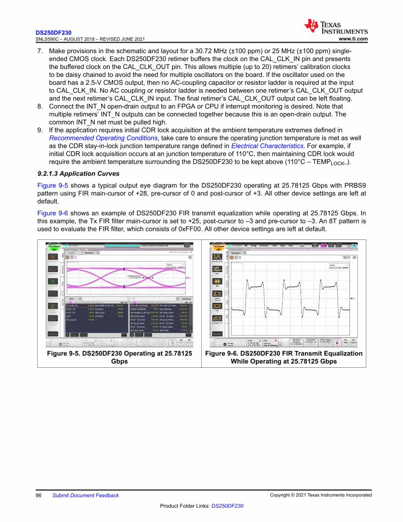
7. Make provisions in the schematic and layout for a 30.72 MHz (±100 ppm) or 25 MHz (±100 ppm) single-ended CMOS clock. Each DS250DF230 retimer buffers the clock on the CAL_CLK_IN pin and presents the buffered clock on the CAL_CLK_OUT pin. This allows multiple (up to 20) retimers’ calibration clocks to be daisy chained to avoid the need for multiple oscillators on the board. If the oscillator used on the board has a 2.5-V CMOS output, then no AC-coupling capacitor or resistor ladder is required at the input to CAL_CLK_IN. No AC coupling or resistor ladder is needed between one retimer’s CAL_CLK_OUT output and the next retimer’s CAL_CLK_IN input. The final retimer’s CAL_CLK_OUT output can be left floating.
8. Connect the INT_N open-drain output to an FPGA or CPU if interrupt monitoring is desired. Note that multiple retimers’ INT_N outputs can be connected together because this is an open-drain output. The common INT_N net must be pulled high.
9. If the application requires initial CDR lock acquisition at the ambient temperature extremes defined in Recommended Operating Conditions, take care to ensure the operating junction temperature is met as well as the CDR stay-in-lock junction temperature range defined in Electrical Characteristics. For example, if initial CDR lock acquisition occurs at an junction temperature of 110°C, then maintaining CDR lock would require the ambient temperature surrounding the DS250DF230 to be kept above (110°C – TEMPLOCK–).
9.2.1.3 Application Curves
Figure 9-5 shows a typical output eye diagram for the DS250DF230 operating at 25.78125 Gbps with PRBS9 pattern using FIR main-cursor of +28, pre-cursor of 0 and post-cursor of +3. All other device settings are left at default.
Figure 9-6 shows an example of DS250DF230 FIR transmit equalization while operating at 25.78125 Gbps. In this example, the Tx FIR filter main-cursor is set to +25, post-cursor to –3 and pre-cursor to –3. An 8T pattern is used to evaluate the FIR filter, which consists of 0xFF00. All other device settings are left at default.
Figure 9-5. DS250DF230 Operating at 25.78125 Gbps
Figure 9-6. DS250DF230 FIR Transmit Equalization While Operating at 25.78125 Gbps
DS250DF230SNLS590C – AUGUST 2018 – REVISED JUNE 2021 www.ti.com
96 Submit Document Feedback Copyright © 2021 Texas Instruments Incorporated
Product Folder Links: DS250DF230
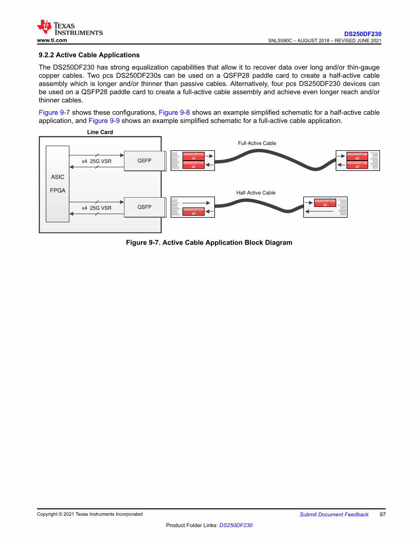
9.2.2 Active Cable Applications
The DS250DF230 has strong equalization capabilities that allow it to recover data over long and/or thin-gauge copper cables. Two pcs DS250DF230s can be used on a QSFP28 paddle card to create a half-active cable assembly which is longer and/or thinner than passive cables. Alternatively, four pcs DS250DF230 devices can be used on a QSFP28 paddle card to create a full-active cable assembly and achieve even longer reach and/or thinner cables.
Figure 9-7 shows these configurations, Figure 9-8 shows an example simplified schematic for a half-active cable application, and Figure 9-9 shows an example simplified schematic for a full-active cable application.
Line Card
x4 25G VSR QSFPDS250DF230
x2
DS250DF230
x2
DS250DF230
x2
DS250DF230
x2
DS250DF230
x2
DS250DF230
x2
Full-Active Cable
Half-Active Cable
x4 25G VSR QSFP
ASIC
FPGA
Figure 9-7. Active Cable Application Block Diagram
www.ti.comDS250DF230
SNLS590C – AUGUST 2018 – REVISED JUNE 2021
Copyright © 2021 Texas Instruments Incorporated Submit Document Feedback 97
Product Folder Links: DS250DF230

No Retimer and no AC coupling capacitors needed
Paddle
card cable
side
Paddle
card host
side
CAL_CLK_IN CAL_CLK_OUT
ADDR0
ADDR1
SDC
ALL_DONE_N
SDA
INT_N
GND
Address straps
(pull-up, pull-
down, or float)
Minimum
recommended
decoupling
RX0PRX0N
RX1N
TX0PTX0N
TX1PTX1N
RX1P
(1) SMBus signals need to be pulled up elsewhere in the system.
TX CDR RX
TX
Output can float
in slave mode
VDD
SMBus
Slave modeEN_SMB
1 N
VDD
READ_EN_NSMBus Slave
mode
0.01 F
(2x)0.1 F
(2x)
2.5 V
X
CDR RX
TEST0 /RCK0
THR /TEST1
RX Retimer
2.5 V or 3.3 V
To other open-
drain interrupt
pins
To system
SMBus
Figure 9-8. Half-Active Cable Application Schematic
DS250DF230SNLS590C – AUGUST 2018 – REVISED JUNE 2021 www.ti.com
98 Submit Document Feedback Copyright © 2021 Texas Instruments Incorporated
Product Folder Links: DS250DF230
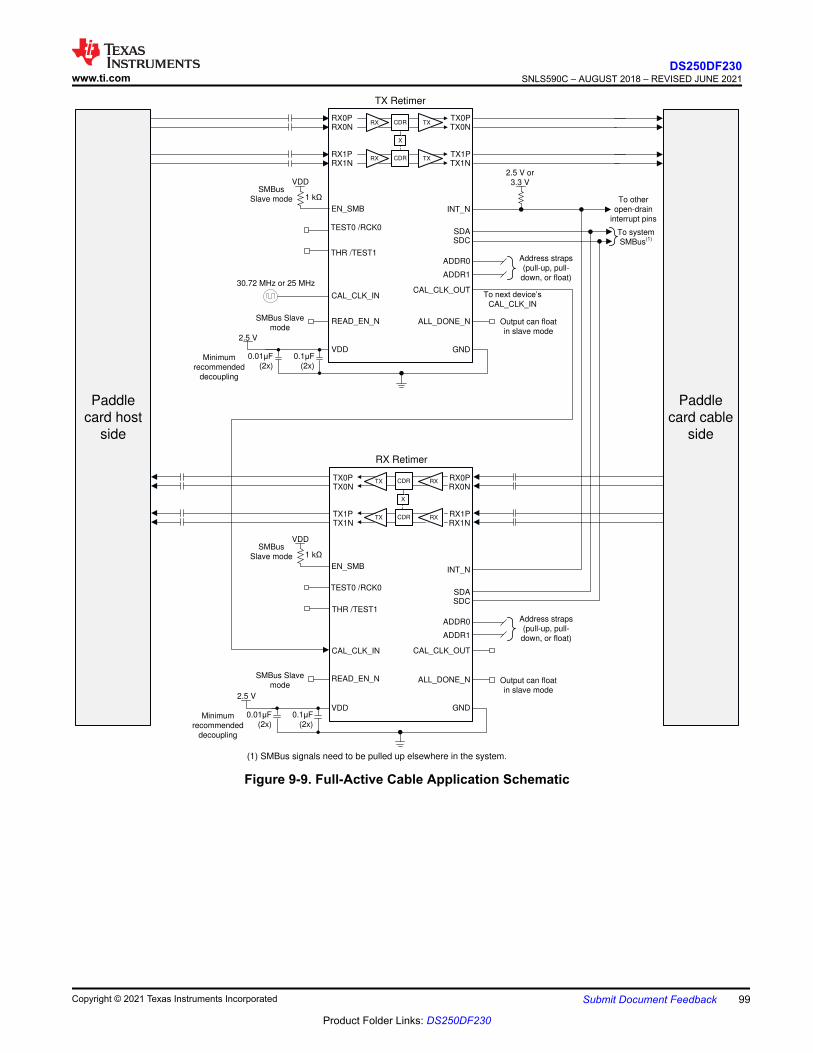
Paddle
card cable
side
Paddle
card host
side
RX0PRX0N
RX1PRX1N
CAL_CLK_OUT
ADDR0
ADDR1
SDC
ALL_DONE_N
SDA
INT_N
TX0PTX0N
TX1PTX1N
GND
7RQH[WGHYLFH¶V
CAL_CLK_IN
2.5 V or
3.3 V
To other
open-drain
interrupt pins
VDDSMBus
Slave mode
RX
EN_SMB
Address straps
(pull-up, pull-
down, or float)
1 N
To system
SMBus(1)
CDR TX
RX TX
Output can float
in slave mode
Minimum
recommended
decoupling
CAL_CLK_IN CAL_CLK_OUT
ADDR0
ADDR1
SDC
ALL_DONE_N
SDA
INT_N
GND
Address straps
(pull-up, pull-
down, or float)
Minimum
recommended
decoupling
RX0PRX0N
RX1N
TX0PTX0N
TX1PTX1N
RX1P
(1) SMBus signals need to be pulled up elsewhere in the system.
TX CDR RX
TX
Output can float
in slave mode
VDD
CAL_CLK_IN
READ_EN_N
30.72 MHz or 25 MHz
0.01F
(2x)
0.1F
(2x)
SMBus Slave
mode
2.5 V
TEST0 /RCK0
THR /TEST1
VDDSMBus
Slave mode
EN_SMB
1 N
VDD
READ_EN_NSMBus Slave
mode
0.01F
(2x)
0.1F
(2x)
2.5 V
X
CDR
X
CDR RX
TEST0 /RCK0
THR /TEST1
TX Retimer
RX Retimer
Figure 9-9. Full-Active Cable Application Schematic
www.ti.comDS250DF230
SNLS590C – AUGUST 2018 – REVISED JUNE 2021
Copyright © 2021 Texas Instruments Incorporated Submit Document Feedback 99
Product Folder Links: DS250DF230

9.2.2.1 Design Requirements
For this design example, the following guidelines outlined in Table 9-2 and Table 9-3 apply.
Table 9-2. Half-Active Cable Application Design GuidelinesDESIGN PARAMETER REQUIREMENT
Device placementPlace the DS250DF230s on the receive side of the paddle card such that it is receiving data from the cable, and transmitting towards the host.
AC-coupling capacitors 100-nF, AC-coupling capacitors are required for the RX inputs and the TX outputs.
Cable insertion loss
The raw cable insertion loss including the insertion loss of the paddle card must be ≤ 27 dB at 25.78125-Gbps Nyquist frequency (12.9 GHz). This is to ensure that the total loss at the input to the DS250DF230 is ≤ 35 dB at 12.9 GHz. Assuming a worst-case host-side PCB loss of 7 dB, plus a connector loss of 1 dB, the remaining loss allocated for the raw cable and paddle cards is 27 dB.
Table 9-3. Full-Active Cable Application Design GuidelinesDESIGN PARAMETER REQUIREMENT
Device placementA full-active QSFP cable will uses 4 pieces of DS250DF230 per paddle card. Typically, two devices will be placed on each side of the paddle card.
AC-coupling capacitors
Transmit-side Retimer: 100-nF, AC coupling capacitors are required for the RX inputs and are not required for the TX outputs. This link segment will be AC coupled on the paddle card at the opposite end of the cable.Receive-side Retimer: 100-nF, AC-coupling capacitors are required for the RX inputs and the TX outputs.
Cable insertion lossThe raw cable insertion loss including the insertion loss of the paddle card must be ≤ 35 dB at 25.78125-Gbps Nyquist frequency (12.9 GHz).
9.2.2.2 Detailed Design Procedure
The design procedure for active cable applications is as follows:
1. Determine the maximum current draw required for one or more of the DS250DF230 retimers on the paddle card. This may impact the selection of the regulator for the 2.5-V supply rail. To calculate the maximum current draw, multiply the maximum transient power supply current by the total number of DS250DF230 devices.
2. Determine the maximum operational power consumption for the purpose of thermal analysis. There are two ways to approach this calculation:a. Maximum mission-mode operational power consumption is when all channels are locked and re-
transmitting the data which is received. PRBS pattern checkers/generators are not used in this mode because normal traffic cannot be checked with a PRBS checker. For this calculation, multiply the worst-case power consumption in mission mode by the total number of DS250DF230 devices.
b. Maximum debug-mode operational power consumption is when all channels are locked and re-transmitting the data which is received. At the same time, some channels’ PRBS checkers or generators may be enabled. For this calculation, multiply the worst-case power consumption in debug mode by the total number of DS250DF230 devices.
3. Determine the SMBus address for one or more of the DS250DF230 retimers. The ADDR[1:0] pins can be left floating for an 8-bit SMBus slave address of 0x44. For the second DS250DF230, a single pullup or pulldown resistor can be used on one address pin. For example, with ADDR0 = Float and ADDR1 = 1 kΩ to GND,the 8-bit SMBus slave address will be 0x34.
DS250DF230SNLS590C – AUGUST 2018 – REVISED JUNE 2021 www.ti.com
100 Submit Document Feedback Copyright © 2021 Texas Instruments Incorporated
Product Folder Links: DS250DF230

4. Determine if the device will be configured from EEPROM (SMBus Master Mode) or from the system I2C bus (SMBus Slave Mode).a. If SMBus Master Mode will be used, provisions must be made for an EEPROM on the board with 8-bit
SMBus address 0xA0. Refer to SMBus Master Mode for more details on SMBus Master Mode including EEPROM size requirements.
b. If SMBus Slave Mode will be used for all device configurations, for example when one or more of the retimers is configured with a microcontroller, an EEPROM is not needed.
5. Make provisions in the schematic and layout for standard decoupling capacitors between the device VDD supply and GND. Refer to the pin function description in Pin Configuration and Functions for more details.
6. Make provisions in the schematic and layout for a 30.72-MHz (±100 ppm) or 25-MHz (±100 ppm) single-ended CMOS clock. The DS250DF230 retimer buffers the clock on the CAL_CLK_IN pin and presents the buffered clock on the CAL_CLK_OUT pin. When using two Retimers on a paddle card, only one 30.72-MHz or 25-MHz clock is required. The CAL_CLK_OUT pin of one retimer can be connected to the CAL_CLK_IN pin of the other retimer.
7. Connect the INT_N open-drain output to the paddle card MCU if interrupt monitoring is desired, otherwise leave it floating. Note that multiple retimers’ INT_N outputs can be connected together because this is an open-drain output. The common INT_N net should be pulled high.
8. If the application requires initial CDR lock acquisition at the ambient temperature extremes defined in Recommended Operating Conditions, take care to ensure the operating junction temperature is met as well as the CDR stay-in-lock junction temperature range defined in Electrical Characteristics. For example, if initial CDR lock acquisition occurs at an junction temperature of 110°C, then maintaining CDR lock would require the junction temperature on DS250DF230 to be kept above (110°C – TEMPLOCK–).
9.2.2.3 Application Curves
See Application Curves in section Front-Port Jitter Cleaning Applications.
www.ti.comDS250DF230
SNLS590C – AUGUST 2018 – REVISED JUNE 2021
Copyright © 2021 Texas Instruments Incorporated Submit Document Feedback 101
Product Folder Links: DS250DF230

9.2.3 Backplane and Mid-Plane Applications
The DS250DF230 has strong equalization capabilities that allow it to recover data over channels up to 35-dB insertion loss. As a result, the optimum placement for the DS250DF230 in a backplane/mid-plane application is with the higher-loss channel segment at the input and the lower-loss channel segment at the output. This reduces the equalization burden on the downstream ASIC/FPGA, as the DS250DF230 is equalizing a majority of the overall channel. This type of asymmetric placement is not a requirement, but when an asymmetric placement is required due to the presence of a passive backplane or mid-plane, then this becomes the recommended placement.
Line CardSwitch Fabric Card
DS
25
0D
F2
30
DS
25
0D
F2
30
ASIC
FPGA
x2 25G
x2 25G
ASIC
FPGA
Co
nn
ecto
r
Co
nn
ecto
r
Passive Backplane/
Midplane
Figure 9-10. Backplane/Mid-Plane Application Block Diagram
DS250DF230SNLS590C – AUGUST 2018 – REVISED JUNE 2021 www.ti.com
102 Submit Document Feedback Copyright © 2021 Texas Instruments Incorporated
Product Folder Links: DS250DF230

ASIC /
FPGA
Backplane
/ Mid-
plane
Connector
RX0PRX0N
RX1PRX1N
CAL_CLK_OUT
ADDR0
ADDR1
SDC
ALL_DONE_N
SDA
INT_N
TX0PTX0N
TX1PTX1N
GND
7RQH[WGHYLFH¶V
CAL_CLK_IN
2.5 V or
3.3 V
To other
open-drain
interrupt pins
VDDSMBus
Slave mode
RX
EN_SMB
Address straps
(pull-up, pull-
down, or float)
1 N
To system
SMBus(1)
CDR TX
RX TX
Output can float
in slave mode
Minimum
recommended
decoupling
CAL_CLK_IN CAL_CLK_OUT
ADDR0
ADDR1
SDC
ALL_DONE_N
SDA
INT_N
GND
Address straps
(pull-up, pull-
down, or float)
Minimum
recommended
decoupling
RX0PRX0N
RX1N
TX0PTX0N
TX1PTX1N
RX1P
(1) SMBus signals need to be pulled up elsewhere in the system.
TX CDR RX
TX
Output can float
in slave mode
VDD
CAL_CLK_IN
READ_EN_N
30.72 MHz or 25 MHz
0.01 F
(2x)
0.1 F
(2x)
SMBus Slavemode
2.5 V
TEST0 /RCK0
THR /TEST1
VDDSMBus
Slave mode
EN_SMB
1 N
VDD
READ_EN_NSMBus Slave
mode
0.01 F
(2x)
0.1 F
(2x)
2.5 V
X
CDR
X
CDR RX
TEST0 /RCK0
THR /TEST1
Figure 9-11. Backplane/Mid-Plane Application Schematic
www.ti.comDS250DF230
SNLS590C – AUGUST 2018 – REVISED JUNE 2021
Copyright © 2021 Texas Instruments Incorporated Submit Document Feedback 103
Product Folder Links: DS250DF230

9.2.3.1 Design Requirements
For this design example, the following guidelines outlined in Table 9-4 apply.
Table 9-4. Backplane/Mid-Plane Application Design GuidelinesDESIGN PARAMETER REQUIREMENT
AC coupling capacitors AC-coupling capacitors in the range of 100 to 220 nF are required for the RX inputs and TX outputs.
Input channel insertion loss ≤ 35 dB at 25.78125-Gbps Nyquist frequency (12.9 GHz)
Output channel insertion lossDepends on downstream ASIC / FPGA capabilities. The DS250DF230 has a low-jitter output driver with 3-tap FIR filter for equalizing a portion of the output channel.
Link partner TX launch amplitude 800 mVppd to 1200 mVppd
Link partner TX FIR filter Depends on channel loss. Refer to the Setting the Output VOD, Pre-Cursor, and Post-Cursor Equalization section.
9.2.3.2 Detailed Design Procedure
The design procedure for backplane/mid-plane applications is as follows:
1. Determine the total number of channels on the board which require a DS250DF230 for signal conditioning. This will dictate the total number of DS250DF230 devices required for the board. It is generally recommended that channels with similar total insertion loss on the board be grouped together in the same DS250DF230 device. This will simplify the device settings, as similar loss channels generally use similar settings.
2. Determine the maximum current draw required for all DS250DF230 retimers. This may impact the selection of the regulator for the 2.5-V supply rail. To calculate the maximum current draw, multiply the maximum transient power supply current by the total number of DS250DF230 devices.
3. Determine the maximum operational power consumption for the purpose of thermal analysis. There are two ways to approach this calculation:a. Maximum mission-mode operational power consumption is when all channels are locked and re-
transmitting the data which is received. PRBS pattern checkers/generators are not used in this mode because normal traffic cannot be checked with a PRBS checker. For this calculation, multiply the worst-case power consumption in mission mode by the total number of DS250DF230 devices.
b. Maximum debug-mode operational power consumption is when all channels are locked and re-transmitting the data which is received. At the same time, some channels’ PRBS checkers or generators may be enabled. For this calculation, multiply the worst-case power consumption in debug mode by the total number of DS250DF230 devices.
4. Determine the SMBus address scheme needed to uniquely address each DS250DF230 device on the board, depending on the total number of devices identified in step 2. Each DS250DF230 can be strapped with one of 16 unique SMBus addresses. If there are more DS250DF230 devices on the board than the number of unique SMBus addresses which can be assigned, then use an I2C expander like the TCA/PCA family of I2C/SMBus switches and multiplexers to split up the SMBus into multiple busses.
5. Determine if the device will be configured from EEPROM (SMBus Master Mode) or from the system I2C bus (SMBus Slave Mode).a. If SMBus Master Mode will be used, provisions must be made for an EEPROM on the board with 8-bit
SMBus address 0xA0. Refer to SMBus Master Mode for more details on SMBus Master Mode including EEPROM size requirements.
b. If SMBus Slave Mode will be used for all device configurations, an EEPROM is not needed.6. Make provisions in the schematic and layout for standard decoupling capacitors between the device VDD
supply and GND. Refer to the pin function description in Pin Configuration and Functions for more details.
DS250DF230SNLS590C – AUGUST 2018 – REVISED JUNE 2021 www.ti.com
104 Submit Document Feedback Copyright © 2021 Texas Instruments Incorporated
Product Folder Links: DS250DF230
7. Make provisions in the schematic and layout for a 30.72-MHz (±100 ppm) or 25-MHz (±100 ppm) single-ended CMOS clock. Each DS250DF230 retimer buffers the clock on the CAL_CLK_IN pin and presents the buffered clock on the CAL_CLK_OUT pin. This allows multiple (up to 20) retimers’ calibration clocks to be daisy chained to avoid the need for multiple oscillators on the board. If the oscillator used on the board has a 2.5-V CMOS output, then no AC-coupling capacitor or resistor ladder is required at the input to CAL_CLK_IN. No AC coupling or resistor ladder is needed between one retimer’s CAL_CLK_OUT output and the next retimer’s CAL_CLK_IN input. The final retimer’s CAL_CLK_OUT output can be left floating.
8. Connect the INT_N open-drain output to an FPGA or CPU if interrupt monitoring is desired. Note that multiple retimers’ INT_N outputs can be connected together because this is an open-drain output. The common INT_N net must be pulled high.
9. If the application requires initial CDR lock acquisition at the ambient temperature extremes defined in Recommended Operating Conditions, take care to ensure the operating junction temperature is met as well as the CDR stay-in-lock junction temperature range defined in Electrical Characteristics. For example, if initial CDR lock acquisition occurs at an junction temperature of 110 °C, then maintaining CDR lock would require the junction temperature on DS250DF230 to be kept above (110°C - TEMPLOCK-).
9.2.3.3 Application Curves
See Application Curves in section Front-Port Jitter Cleaning Applications.
10 Power Supply RecommendationsFollow these general guidelines when designing the power supply:1. The power supply must be designed to provide the recommended operating conditions outlined in
Specifications in terms of DC voltage, AC noise, and start-up ramp time.2. The maximum current draw for the DS250DF230 is provided in Specifications. This figure can be used to
calculate the maximum current the power supply must provide. Typical mission-mode current draw can be inferred from the typical power consumption in Specifications.
3. The DS250DF230 does not require any special power supply filtering (that is, ferrite bead), provided the recommended operating conditions are met. Only standard supply decoupling is required. Refer to the Pin Configuration and Functions section for details concerning the recommended supply decoupling.
www.ti.comDS250DF230
SNLS590C – AUGUST 2018 – REVISED JUNE 2021
Copyright © 2021 Texas Instruments Incorporated Submit Document Feedback 105
Product Folder Links: DS250DF230

11 Layout11.1 Layout GuidelinesFollow these guidelines when designing the layout:1. Decoupling capacitors must be placed as close to the VDD pins as possible. Placing them directly
underneath the device is one option if the board design permits.2. High-speed differential signals TXnP/TXnN and RXnP/RXnN must be tightly coupled, skew matched, and
impedance controlled.3. Vias must be avoided when possible on the high-speed differential signals. When vias must be used, take
care to minimize the via stub, either by transitioning through most or all layers, or by back drilling.4. GND relief can be used beneath the high-speed differential signal pads to improve signal integrity by
counteracting the pad capacitance.5. GND relief can be used beneath the AC-coupling capacitor pads to improve signal integrity by counteracting
the pad capacitance.6. GND vias must be placed directly beneath the device connecting the GND plane attached to the device
to the GND planes on other layers. This has the added benefit of improving thermal conductivity from the device to the board.
7. If vias are used for the high-speed signals, the ground via must be implemented adjacent to the signal via to provide return path and isolation. For differential pair, the typical via configuration is ground-signal-signal-ground.
11.2 Layout ExamplesThe example layouts in Figure 11-1 through Figure 11-5 demonstrate how all signals can be escaped from the BGA array using microstrip routing on a generic multi-layer stackup.
Figure 11-1. Top Layer Figure 11-2. Layer 1 GND
Figure 11-3. Internal Low-Speed Signal Layers Figure 11-4. VDD Layer
DS250DF230SNLS590C – AUGUST 2018 – REVISED JUNE 2021 www.ti.com
106 Submit Document Feedback Copyright © 2021 Texas Instruments Incorporated
Product Folder Links: DS250DF230

Figure 11-5. Bottom Layer
www.ti.comDS250DF230
SNLS590C – AUGUST 2018 – REVISED JUNE 2021
Copyright © 2021 Texas Instruments Incorporated Submit Document Feedback 107
Product Folder Links: DS250DF230
12 Device and Documentation Support12.1 Device Support12.1.1 Development Support
For additional information, see TI’s Surface Mount Technology (SMT) References at:
http://focus.ti.com/quality/docs under the Quality & Lead (Pb)-Free Data menu.
For device and channel model simulation, refer to the DS250DF230 IBIS-AMI Model:
• Texas Instruments, DS250DF230 IBIS-AMI Model IBIS Model
Click here to request access to the DS250DF230 IBIS-AMI Model (SNLM215) in the DS250DF230 MySecure folder.
12.2 Documentation Support12.2.1 Related Documentation
For related documentation, see the following:
• Texas Instruments DS2x0DF810, DS250DFx10, DS250DF230 Programmer's Guide
Click here to request access to the DS250DF230 Programming Guide in the DS250DF230 MySecure folder.
12.3 Receiving Notification of Documentation UpdatesTo receive notification of documentation updates, navigate to the device product folder on ti.com. Click on Subscribe to updates to register and receive a weekly digest of any product information that has changed. For change details, review the revision history included in any revised document.
12.4 Support ResourcesTI E2E™ support forums are an engineer's go-to source for fast, verified answers and design help — straight from the experts. Search existing answers or ask your own question to get the quick design help you need.
Linked content is provided "AS IS" by the respective contributors. They do not constitute TI specifications and do not necessarily reflect TI's views; see TI's Terms of Use.
12.5 TrademarksTI E2E™ is a trademark of Texas Instruments.All trademarks are the property of their respective owners.
13 Electrostatic Discharge CautionThis integrated circuit can be damaged by ESD. Texas Instruments recommends that all integrated circuits be handled with appropriate precautions. Failure to observe proper handling and installation procedures can cause damage.ESD damage can range from subtle performance degradation to complete device failure. Precision integrated circuits may be more susceptible to damage because very small parametric changes could cause the device not to meet its published specifications.
14 GlossaryTI Glossary This glossary lists and explains terms, acronyms, and definitions.
15 Mechanical, Packaging, and Orderable InformationThe following pages include mechanical, packaging, and orderable information. This information is the most current data available for the designated devices. This data is subject to change without notice and revision of this document. For browser-based versions of this data sheet, refer to the left-hand navigation.
DS250DF230SNLS590C – AUGUST 2018 – REVISED JUNE 2021 www.ti.com
108 Submit Document Feedback Copyright © 2021 Texas Instruments Incorporated
Product Folder Links: DS250DF230

PACKAGE OPTION ADDENDUM
www.ti.com 9-Jul-2021
Addendum-Page 1
PACKAGING INFORMATION
Orderable Device Status(1)
Package Type PackageDrawing
Pins PackageQty
Eco Plan(2)
Lead finish/Ball material
(6)
MSL Peak Temp(3)
Op Temp (°C) Device Marking(4/5)
Samples
DS250DF230RTVR ACTIVE WQFN RTV 32 3000 RoHS & Green NIPDAU Level-2-260C-1 YEAR -40 to 85 DS250DF2
DS250DF230RTVT ACTIVE WQFN RTV 32 250 RoHS & Green NIPDAU Level-2-260C-1 YEAR -40 to 85 DS250DF2
DS250DF230ZLSR ACTIVE NFBGA ZLS 36 3000 RoHS & Green SNAGCU Level-3-260C-168 HR -40 to 85 D250DF230
DS250DF230ZLST ACTIVE NFBGA ZLS 36 250 RoHS & Green SNAGCU Level-3-260C-168 HR -40 to 85 D250DF230
(1) The marketing status values are defined as follows:ACTIVE: Product device recommended for new designs.LIFEBUY: TI has announced that the device will be discontinued, and a lifetime-buy period is in effect.NRND: Not recommended for new designs. Device is in production to support existing customers, but TI does not recommend using this part in a new design.PREVIEW: Device has been announced but is not in production. Samples may or may not be available.OBSOLETE: TI has discontinued the production of the device.
(2) RoHS: TI defines "RoHS" to mean semiconductor products that are compliant with the current EU RoHS requirements for all 10 RoHS substances, including the requirement that RoHS substancedo not exceed 0.1% by weight in homogeneous materials. Where designed to be soldered at high temperatures, "RoHS" products are suitable for use in specified lead-free processes. TI mayreference these types of products as "Pb-Free".RoHS Exempt: TI defines "RoHS Exempt" to mean products that contain lead but are compliant with EU RoHS pursuant to a specific EU RoHS exemption.Green: TI defines "Green" to mean the content of Chlorine (Cl) and Bromine (Br) based flame retardants meet JS709B low halogen requirements of <=1000ppm threshold. Antimony trioxide basedflame retardants must also meet the <=1000ppm threshold requirement.
(3) MSL, Peak Temp. - The Moisture Sensitivity Level rating according to the JEDEC industry standard classifications, and peak solder temperature.
(4) There may be additional marking, which relates to the logo, the lot trace code information, or the environmental category on the device.
(5) Multiple Device Markings will be inside parentheses. Only one Device Marking contained in parentheses and separated by a "~" will appear on a device. If a line is indented then it is a continuationof the previous line and the two combined represent the entire Device Marking for that device.
(6) Lead finish/Ball material - Orderable Devices may have multiple material finish options. Finish options are separated by a vertical ruled line. Lead finish/Ball material values may wrap to twolines if the finish value exceeds the maximum column width.
Important Information and Disclaimer:The information provided on this page represents TI's knowledge and belief as of the date that it is provided. TI bases its knowledge and belief on informationprovided by third parties, and makes no representation or warranty as to the accuracy of such information. Efforts are underway to better integrate information from third parties. TI has taken and

PACKAGE OPTION ADDENDUM
www.ti.com 9-Jul-2021
Addendum-Page 2
continues to take reasonable steps to provide representative and accurate information but may not have conducted destructive testing or chemical analysis on incoming materials and chemicals.TI and TI suppliers consider certain information to be proprietary, and thus CAS numbers and other limited information may not be available for release.
In no event shall TI's liability arising out of such information exceed the total purchase price of the TI part(s) at issue in this document sold by TI to Customer on an annual basis.
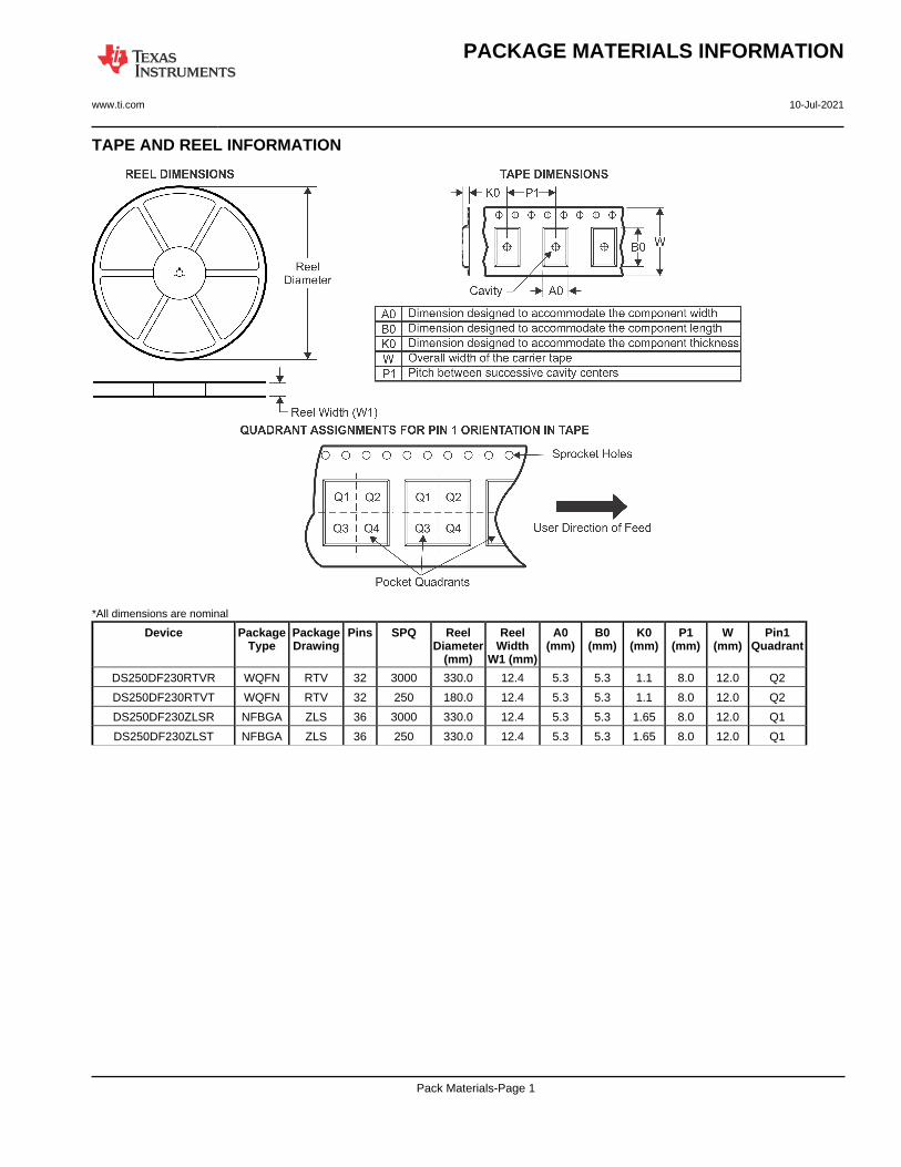
TAPE AND REEL INFORMATION
*All dimensions are nominal
Device PackageType
PackageDrawing
Pins SPQ ReelDiameter
(mm)
ReelWidth
W1 (mm)
A0(mm)
B0(mm)
K0(mm)
P1(mm)
W(mm)
Pin1Quadrant
DS250DF230RTVR WQFN RTV 32 3000 330.0 12.4 5.3 5.3 1.1 8.0 12.0 Q2
DS250DF230RTVT WQFN RTV 32 250 180.0 12.4 5.3 5.3 1.1 8.0 12.0 Q2
DS250DF230ZLSR NFBGA ZLS 36 3000 330.0 12.4 5.3 5.3 1.65 8.0 12.0 Q1
DS250DF230ZLST NFBGA ZLS 36 250 330.0 12.4 5.3 5.3 1.65 8.0 12.0 Q1
PACKAGE MATERIALS INFORMATION
www.ti.com 10-Jul-2021
Pack Materials-Page 1

*All dimensions are nominal
Device Package Type Package Drawing Pins SPQ Length (mm) Width (mm) Height (mm)
DS250DF230RTVR WQFN RTV 32 3000 367.0 367.0 35.0
DS250DF230RTVT WQFN RTV 32 250 210.0 185.0 35.0
DS250DF230ZLSR NFBGA ZLS 36 3000 336.6 336.6 31.8
DS250DF230ZLST NFBGA ZLS 36 250 336.6 336.6 31.8
PACKAGE MATERIALS INFORMATION
www.ti.com 10-Jul-2021
Pack Materials-Page 2

www.ti.com
PACKAGE OUTLINE
C
32X 0.300.18
3.45 0.1
32X 0.50.3
0.80.7
(DIM A) TYP
0.050.00
28X 0.5
2X3.5
2X 3.5
A 5.154.85
B
5.154.85
(0.2) TYP
WQFN - 0.8 mm max heightRTV0032EPLASTIC QUAD FLATPACK - NO LEAD
4225196/A 08/2019
SIDE WALL LEAD METAL THICKNESS
DIM AOPTION 1 OPTION 2
0.1 0.2
PIN 1 INDEX AREA
0.08 C
SEATING PLANE
1
817
24
9 16
32 25(OPTIONAL)PIN 1 ID
0.1 C A B0.05 C
EXPOSEDTHERMAL PAD
33 SYMM
SYMM
NOTES: 1. All linear dimensions are in millimeters. Any dimensions in parenthesis are for reference only. Dimensioning and tolerancing per ASME Y14.5M. 2. This drawing is subject to change without notice. 3. The package thermal pad must be soldered to the printed circuit board for thermal and mechanical performance.
SCALE 3.000

www.ti.com
EXAMPLE BOARD LAYOUT
(1.475)
0.07 MINALL AROUND
0.07 MAXALL AROUND
32X (0.24)
32X (0.6)
( 0.2) TYPVIA
28X (0.5)
(4.8)
(4.8)
(1.475)
( 3.45)
(R0.05)TYP
WQFN - 0.8 mm max heightRTV0032EPLASTIC QUAD FLATPACK - NO LEAD
4225196/A 08/2019
SYMM
1
8
9 16
17
24
2532
SYMM
LAND PATTERN EXAMPLESCALE:18X
NOTES: (continued) 4. This package is designed to be soldered to a thermal pad on the board. For more information, see Texas Instruments literature number SLUA271 (www.ti.com/lit/slua271).5. Vias are optional depending on application, refer to device data sheet. If any vias are implemented, refer to their locations shown on this view. It is recommended that vias under paste be filled, plugged or tented.
33
SOLDER MASKOPENING
METAL UNDERSOLDER MASK
SOLDER MASKDEFINED
METAL
SOLDER MASKOPENING
SOLDER MASK DETAILS
NON SOLDER MASKDEFINED
(PREFERRED)

www.ti.com
EXAMPLE STENCIL DESIGN
32X (0.6)
32X (0.24)
28X (0.5)
(4.8)
(4.8)
4X ( 1.49)
(0.845)
(0.845)(R0.05) TYP
WQFN - 0.8 mm max heightRTV0032EPLASTIC QUAD FLATPACK - NO LEAD
4225196/A 08/2019
NOTES: (continued) 6. Laser cutting apertures with trapezoidal walls and rounded corners may offer better paste release. IPC-7525 may have alternate design recommendations.
33
SYMM
METALTYP
SOLDER PASTE EXAMPLEBASED ON 0.125 mm THICK STENCIL
EXPOSED PAD 33:
75% PRINTED SOLDER COVERAGE BY AREA UNDER PACKAGESCALE:20X
SYMM
1
8
9 16
17
24
2532

www.ti.com
PACKAGE OUTLINE
C1.41 MAX
TYP0.350.23
0.8 TYP
0.8 TYP
4TYP
4 TYP
36X -0.450.35
B 5.14.9
A
5.14.9
NFBGA - 1.41 mm max heightZLS0036ABALL GRID ARRAY
4220412/A 04/2017
NOTES: 1. All linear dimensions are in millimeters. Any dimensions in parenthesis are for reference only. Dimensioning and tolerancing per ASME Y14.5M. 2. This drawing is subject to change without notice.
BALL A1CORNER
SEATING PLANE
BALL TYP 0.1 C
SCALE 2.500
B
A
1 2 3
0.15 C A B0.08 C
SYMM
SYMM
4BALL A1 CORNER
5 6
E
D
C
F

www.ti.com
EXAMPLE BOARD LAYOUT
36X ( 0.35)(0.8) TYP
(0.8) TYP
( 0.35)METAL
0.05 MAX
SOLDER MASKOPENING
METAL UNDERSOLDER MASK
( 0.35)SOLDER MASKOPENING
0.05 MIN
NFBGA - 1.41 mm max heightZLS0036ABALL GRID ARRAY
4220412/A 04/2017
NOTES: (continued) 3. Final dimensions may vary due to manufacturing tolerance considerations and also routing constraints. For more information, see Texas Instruments Literature number SPRAA99 (www.ti.com/lit/spraa99).
SYMM
SYMM
LAND PATTERN EXAMPLEEXPOSED METAL SHOWN
SCALE:15X
1 2 3 4
F
E
D
C
B
A5 6
NON-SOLDER MASKDEFINED
(PREFERRED)
SOLDER MASK DETAILSNOT TO SCALE
EXPOSED METAL
SOLDER MASKDEFINED
EXPOSED METAL

www.ti.com
EXAMPLE STENCIL DESIGN
(0.8) TYP
(0.8) TYP 36X ( 0.35)
NFBGA - 1.41 mm max heightZLS0036ABALL GRID ARRAY
4220412/A 04/2017
NOTES: (continued) 4. Laser cutting apertures with trapezoidal walls and rounded corners may offer better paste release.
SYMM
SYMM
SOLDER PASTE EXAMPLEBASED ON 0.15 mm THICK STENCIL
SCALE:15X
1 2 3 4
F
E
D
C
B
A5 6

IMPORTANT NOTICE AND DISCLAIMERTI PROVIDES TECHNICAL AND RELIABILITY DATA (INCLUDING DATASHEETS), DESIGN RESOURCES (INCLUDING REFERENCEDESIGNS), APPLICATION OR OTHER DESIGN ADVICE, WEB TOOLS, SAFETY INFORMATION, AND OTHER RESOURCES “AS IS”AND WITH ALL FAULTS, AND DISCLAIMS ALL WARRANTIES, EXPRESS AND IMPLIED, INCLUDING WITHOUT LIMITATION ANYIMPLIED WARRANTIES OF MERCHANTABILITY, FITNESS FOR A PARTICULAR PURPOSE OR NON-INFRINGEMENT OF THIRDPARTY INTELLECTUAL PROPERTY RIGHTS.These resources are intended for skilled developers designing with TI products. You are solely responsible for (1) selecting the appropriateTI products for your application, (2) designing, validating and testing your application, and (3) ensuring your application meets applicablestandards, and any other safety, security, or other requirements. These resources are subject to change without notice. TI grants youpermission to use these resources only for development of an application that uses the TI products described in the resource. Otherreproduction and display of these resources is prohibited. No license is granted to any other TI intellectual property right or to any third partyintellectual property right. TI disclaims responsibility for, and you will fully indemnify TI and its representatives against, any claims, damages,costs, losses, and liabilities arising out of your use of these resources.TI’s products are provided subject to TI’s Terms of Sale (https:www.ti.com/legal/termsofsale.html) or other applicable terms available eitheron ti.com or provided in conjunction with such TI products. TI’s provision of these resources does not expand or otherwise alter TI’sapplicable warranties or warranty disclaimers for TI products.IMPORTANT NOTICE
Mailing Address: Texas Instruments, Post Office Box 655303, Dallas, Texas 75265Copyright © 2021, Texas Instruments Incorporated