dsp builder reference manual - altera · 2018-04-26 · dsp builder reference manual software...
TRANSCRIPT

101 Innovation DriveSan Jose, CA 95134www.altera.com
DSP BuilderReference Manual
Software Version: 9.1 SP1Document Date: January 2010

Copyright © 2010 Altera Corporation. All rights reserved. Altera, The Programmable Solutions Company, the stylized Altera logo, specific device designations, and all otherwords and logos that are identified as trademarks and/or service marks are, unless noted otherwise, the trademarks and service marks of Altera Corporation in the U.S. and othercountries. All other product or service names are the property of their respective holders. Altera products are protected under numerous U.S. and foreign patents and pending ap-plications, maskwork rights, and copyrights. Altera warrants performance of its semiconductor products to current specifications in accordance with Altera's standard warranty,but reserves the right to make changes to any products and services at any time without notice. Altera assumes no responsibility or liability arising out of the application or use ofany information, product, or service described herein except as expressly agreed to in writing by Altera Corporation. Altera customers are advised to obtain the latest version ofdevice specifications before relying on any published information and before placing orders for products or services.
MNL-DSPBLDR-9.2

© January 2010 Altera Corporation
Contents
Chapter 1. AltLab LibraryBP (Bus Probe) . . . . . . . . . . . . . . . . . . . . . . . . . . . . . . . . . . . . . . . . . . . . . . . . . . . . . . . . . . . . . . . . . . . . . . . . . 1–2Clock . . . . . . . . . . . . . . . . . . . . . . . . . . . . . . . . . . . . . . . . . . . . . . . . . . . . . . . . . . . . . . . . . . . . . . . . . . . . . . . . . 1–2Clock_Derived . . . . . . . . . . . . . . . . . . . . . . . . . . . . . . . . . . . . . . . . . . . . . . . . . . . . . . . . . . . . . . . . . . . . . . . . . 1–3Display Pipeline Depth . . . . . . . . . . . . . . . . . . . . . . . . . . . . . . . . . . . . . . . . . . . . . . . . . . . . . . . . . . . . . . . . . 1–4HDL Entity . . . . . . . . . . . . . . . . . . . . . . . . . . . . . . . . . . . . . . . . . . . . . . . . . . . . . . . . . . . . . . . . . . . . . . . . . . . . 1–4HDL Import . . . . . . . . . . . . . . . . . . . . . . . . . . . . . . . . . . . . . . . . . . . . . . . . . . . . . . . . . . . . . . . . . . . . . . . . . . . 1–5HDL Input . . . . . . . . . . . . . . . . . . . . . . . . . . . . . . . . . . . . . . . . . . . . . . . . . . . . . . . . . . . . . . . . . . . . . . . . . . . . 1–7HDL Output . . . . . . . . . . . . . . . . . . . . . . . . . . . . . . . . . . . . . . . . . . . . . . . . . . . . . . . . . . . . . . . . . . . . . . . . . . . 1–8HIL (Hardware in the Loop) . . . . . . . . . . . . . . . . . . . . . . . . . . . . . . . . . . . . . . . . . . . . . . . . . . . . . . . . . . . . . 1–9Quartus II Global Project Assignment . . . . . . . . . . . . . . . . . . . . . . . . . . . . . . . . . . . . . . . . . . . . . . . . . . . . 1–11Quartus II Pinout Assignments . . . . . . . . . . . . . . . . . . . . . . . . . . . . . . . . . . . . . . . . . . . . . . . . . . . . . . . . . 1–12Resource Usage . . . . . . . . . . . . . . . . . . . . . . . . . . . . . . . . . . . . . . . . . . . . . . . . . . . . . . . . . . . . . . . . . . . . . . . 1–13Signal Compiler . . . . . . . . . . . . . . . . . . . . . . . . . . . . . . . . . . . . . . . . . . . . . . . . . . . . . . . . . . . . . . . . . . . . . . . 1–13SignalTap II Logic Analyzer . . . . . . . . . . . . . . . . . . . . . . . . . . . . . . . . . . . . . . . . . . . . . . . . . . . . . . . . . . . . 1–14SignalTap II Node . . . . . . . . . . . . . . . . . . . . . . . . . . . . . . . . . . . . . . . . . . . . . . . . . . . . . . . . . . . . . . . . . . . . . 1–16Subsystem Builder . . . . . . . . . . . . . . . . . . . . . . . . . . . . . . . . . . . . . . . . . . . . . . . . . . . . . . . . . . . . . . . . . . . . 1–16TestBench . . . . . . . . . . . . . . . . . . . . . . . . . . . . . . . . . . . . . . . . . . . . . . . . . . . . . . . . . . . . . . . . . . . . . . . . . . . . 1–17VCD Sink . . . . . . . . . . . . . . . . . . . . . . . . . . . . . . . . . . . . . . . . . . . . . . . . . . . . . . . . . . . . . . . . . . . . . . . . . . . . 1–18
Chapter 2. Arithmetic LibraryBarrel Shifter . . . . . . . . . . . . . . . . . . . . . . . . . . . . . . . . . . . . . . . . . . . . . . . . . . . . . . . . . . . . . . . . . . . . . . . . . . 2–2Bit Level Sum of Products . . . . . . . . . . . . . . . . . . . . . . . . . . . . . . . . . . . . . . . . . . . . . . . . . . . . . . . . . . . . . . . 2–3Comparator . . . . . . . . . . . . . . . . . . . . . . . . . . . . . . . . . . . . . . . . . . . . . . . . . . . . . . . . . . . . . . . . . . . . . . . . . . . 2–5Counter . . . . . . . . . . . . . . . . . . . . . . . . . . . . . . . . . . . . . . . . . . . . . . . . . . . . . . . . . . . . . . . . . . . . . . . . . . . . . . . 2–6Differentiator . . . . . . . . . . . . . . . . . . . . . . . . . . . . . . . . . . . . . . . . . . . . . . . . . . . . . . . . . . . . . . . . . . . . . . . . . . 2–8Divider . . . . . . . . . . . . . . . . . . . . . . . . . . . . . . . . . . . . . . . . . . . . . . . . . . . . . . . . . . . . . . . . . . . . . . . . . . . . . . . 2–9DSP . . . . . . . . . . . . . . . . . . . . . . . . . . . . . . . . . . . . . . . . . . . . . . . . . . . . . . . . . . . . . . . . . . . . . . . . . . . . . . . . . 2–10Gain . . . . . . . . . . . . . . . . . . . . . . . . . . . . . . . . . . . . . . . . . . . . . . . . . . . . . . . . . . . . . . . . . . . . . . . . . . . . . . . . . 2–15Increment Decrement . . . . . . . . . . . . . . . . . . . . . . . . . . . . . . . . . . . . . . . . . . . . . . . . . . . . . . . . . . . . . . . . . . 2–17Integrator . . . . . . . . . . . . . . . . . . . . . . . . . . . . . . . . . . . . . . . . . . . . . . . . . . . . . . . . . . . . . . . . . . . . . . . . . . . . 2–19Magnitude . . . . . . . . . . . . . . . . . . . . . . . . . . . . . . . . . . . . . . . . . . . . . . . . . . . . . . . . . . . . . . . . . . . . . . . . . . . 2–21Multiplier . . . . . . . . . . . . . . . . . . . . . . . . . . . . . . . . . . . . . . . . . . . . . . . . . . . . . . . . . . . . . . . . . . . . . . . . . . . . 2–21Multiply Accumulate . . . . . . . . . . . . . . . . . . . . . . . . . . . . . . . . . . . . . . . . . . . . . . . . . . . . . . . . . . . . . . . . . . 2–24Multiply Add . . . . . . . . . . . . . . . . . . . . . . . . . . . . . . . . . . . . . . . . . . . . . . . . . . . . . . . . . . . . . . . . . . . . . . . . . 2–26Parallel Adder Subtractor . . . . . . . . . . . . . . . . . . . . . . . . . . . . . . . . . . . . . . . . . . . . . . . . . . . . . . . . . . . . . . 2–28Pipelined Adder . . . . . . . . . . . . . . . . . . . . . . . . . . . . . . . . . . . . . . . . . . . . . . . . . . . . . . . . . . . . . . . . . . . . . . 2–30Product . . . . . . . . . . . . . . . . . . . . . . . . . . . . . . . . . . . . . . . . . . . . . . . . . . . . . . . . . . . . . . . . . . . . . . . . . . . . . . 2–31SOP Tap . . . . . . . . . . . . . . . . . . . . . . . . . . . . . . . . . . . . . . . . . . . . . . . . . . . . . . . . . . . . . . . . . . . . . . . . . . . . . 2–34Square Root . . . . . . . . . . . . . . . . . . . . . . . . . . . . . . . . . . . . . . . . . . . . . . . . . . . . . . . . . . . . . . . . . . . . . . . . . . 2–35Sum of Products . . . . . . . . . . . . . . . . . . . . . . . . . . . . . . . . . . . . . . . . . . . . . . . . . . . . . . . . . . . . . . . . . . . . . . 2–37
Chapter 3. Complex Type LibraryButterfly . . . . . . . . . . . . . . . . . . . . . . . . . . . . . . . . . . . . . . . . . . . . . . . . . . . . . . . . . . . . . . . . . . . . . . . . . . . . . . 3–2Complex AddSub . . . . . . . . . . . . . . . . . . . . . . . . . . . . . . . . . . . . . . . . . . . . . . . . . . . . . . . . . . . . . . . . . . . . . . 3–4Complex Conjugate . . . . . . . . . . . . . . . . . . . . . . . . . . . . . . . . . . . . . . . . . . . . . . . . . . . . . . . . . . . . . . . . . . . . 3–6Complex Constant . . . . . . . . . . . . . . . . . . . . . . . . . . . . . . . . . . . . . . . . . . . . . . . . . . . . . . . . . . . . . . . . . . . . . 3–8Complex Delay . . . . . . . . . . . . . . . . . . . . . . . . . . . . . . . . . . . . . . . . . . . . . . . . . . . . . . . . . . . . . . . . . . . . . . . . 3–9
DSP Builder Reference Manual

iv Contents
Complex Multiplexer . . . . . . . . . . . . . . . . . . . . . . . . . . . . . . . . . . . . . . . . . . . . . . . . . . . . . . . . . . . . . . . . . . 3–10Complex Product . . . . . . . . . . . . . . . . . . . . . . . . . . . . . . . . . . . . . . . . . . . . . . . . . . . . . . . . . . . . . . . . . . . . . 3–11Complex to Real-Imag . . . . . . . . . . . . . . . . . . . . . . . . . . . . . . . . . . . . . . . . . . . . . . . . . . . . . . . . . . . . . . . . . 3–13Real-Imag to Complex . . . . . . . . . . . . . . . . . . . . . . . . . . . . . . . . . . . . . . . . . . . . . . . . . . . . . . . . . . . . . . . . . 3–14
Chapter 4. Gate & Control LibraryBinary to Seven Segments . . . . . . . . . . . . . . . . . . . . . . . . . . . . . . . . . . . . . . . . . . . . . . . . . . . . . . . . . . . . . . . 4–2Bitwise Logical Bus Operator . . . . . . . . . . . . . . . . . . . . . . . . . . . . . . . . . . . . . . . . . . . . . . . . . . . . . . . . . . . . 4–3Case Statement . . . . . . . . . . . . . . . . . . . . . . . . . . . . . . . . . . . . . . . . . . . . . . . . . . . . . . . . . . . . . . . . . . . . . . . . 4–5Decoder . . . . . . . . . . . . . . . . . . . . . . . . . . . . . . . . . . . . . . . . . . . . . . . . . . . . . . . . . . . . . . . . . . . . . . . . . . . . . . . 4–7Demultiplexer . . . . . . . . . . . . . . . . . . . . . . . . . . . . . . . . . . . . . . . . . . . . . . . . . . . . . . . . . . . . . . . . . . . . . . . . . 4–8Flipflop . . . . . . . . . . . . . . . . . . . . . . . . . . . . . . . . . . . . . . . . . . . . . . . . . . . . . . . . . . . . . . . . . . . . . . . . . . . . . . 4–10If Statement . . . . . . . . . . . . . . . . . . . . . . . . . . . . . . . . . . . . . . . . . . . . . . . . . . . . . . . . . . . . . . . . . . . . . . . . . . 4–11LFSR Sequence . . . . . . . . . . . . . . . . . . . . . . . . . . . . . . . . . . . . . . . . . . . . . . . . . . . . . . . . . . . . . . . . . . . . . . . 4–14Logical Bit Operator . . . . . . . . . . . . . . . . . . . . . . . . . . . . . . . . . . . . . . . . . . . . . . . . . . . . . . . . . . . . . . . . . . . 4–16Logical Bus Operator . . . . . . . . . . . . . . . . . . . . . . . . . . . . . . . . . . . . . . . . . . . . . . . . . . . . . . . . . . . . . . . . . . 4–17Logical Reduce Operator . . . . . . . . . . . . . . . . . . . . . . . . . . . . . . . . . . . . . . . . . . . . . . . . . . . . . . . . . . . . . . . 4–19Multiplexer . . . . . . . . . . . . . . . . . . . . . . . . . . . . . . . . . . . . . . . . . . . . . . . . . . . . . . . . . . . . . . . . . . . . . . . . . . . 4–21Pattern . . . . . . . . . . . . . . . . . . . . . . . . . . . . . . . . . . . . . . . . . . . . . . . . . . . . . . . . . . . . . . . . . . . . . . . . . . . . . . . 4–22Single Pulse . . . . . . . . . . . . . . . . . . . . . . . . . . . . . . . . . . . . . . . . . . . . . . . . . . . . . . . . . . . . . . . . . . . . . . . . . . 4–24
Chapter 5. Interfaces LibraryAvalon Memory-Mapped Blocks . . . . . . . . . . . . . . . . . . . . . . . . . . . . . . . . . . . . . . . . . . . . . . . . . . . . . . . . . . 5–1
Avalon-MM Master . . . . . . . . . . . . . . . . . . . . . . . . . . . . . . . . . . . . . . . . . . . . . . . . . . . . . . . . . . . . . . . . . . . . 5–3Avalon-MM Slave . . . . . . . . . . . . . . . . . . . . . . . . . . . . . . . . . . . . . . . . . . . . . . . . . . . . . . . . . . . . . . . . . . . . . . 5–6Avalon-MM Read FIFO . . . . . . . . . . . . . . . . . . . . . . . . . . . . . . . . . . . . . . . . . . . . . . . . . . . . . . . . . . . . . . . . . 5–9Avalon-MM Write FIFO . . . . . . . . . . . . . . . . . . . . . . . . . . . . . . . . . . . . . . . . . . . . . . . . . . . . . . . . . . . . . . . . 5–11
Avalon Streaming Blocks . . . . . . . . . . . . . . . . . . . . . . . . . . . . . . . . . . . . . . . . . . . . . . . . . . . . . . . . . . . . . . . . 5–12Avalon-ST Packet Format Converter . . . . . . . . . . . . . . . . . . . . . . . . . . . . . . . . . . . . . . . . . . . . . . . . . . . . . 5–12Avalon-ST Sink . . . . . . . . . . . . . . . . . . . . . . . . . . . . . . . . . . . . . . . . . . . . . . . . . . . . . . . . . . . . . . . . . . . . . . . 5–19Avalon-ST Source . . . . . . . . . . . . . . . . . . . . . . . . . . . . . . . . . . . . . . . . . . . . . . . . . . . . . . . . . . . . . . . . . . . . . 5–20
Chapter 6. IO & Bus LibraryAltBus . . . . . . . . . . . . . . . . . . . . . . . . . . . . . . . . . . . . . . . . . . . . . . . . . . . . . . . . . . . . . . . . . . . . . . . . . . . . . . . . 6–2Binary Point Casting . . . . . . . . . . . . . . . . . . . . . . . . . . . . . . . . . . . . . . . . . . . . . . . . . . . . . . . . . . . . . . . . . . . . 6–4Bus Builder . . . . . . . . . . . . . . . . . . . . . . . . . . . . . . . . . . . . . . . . . . . . . . . . . . . . . . . . . . . . . . . . . . . . . . . . . . . . 6–5Bus Concatenation . . . . . . . . . . . . . . . . . . . . . . . . . . . . . . . . . . . . . . . . . . . . . . . . . . . . . . . . . . . . . . . . . . . . . 6–7Bus Conversion . . . . . . . . . . . . . . . . . . . . . . . . . . . . . . . . . . . . . . . . . . . . . . . . . . . . . . . . . . . . . . . . . . . . . . . . 6–8Bus Splitter . . . . . . . . . . . . . . . . . . . . . . . . . . . . . . . . . . . . . . . . . . . . . . . . . . . . . . . . . . . . . . . . . . . . . . . . . . . . 6–9Constant . . . . . . . . . . . . . . . . . . . . . . . . . . . . . . . . . . . . . . . . . . . . . . . . . . . . . . . . . . . . . . . . . . . . . . . . . . . . . 6–10Extract Bit . . . . . . . . . . . . . . . . . . . . . . . . . . . . . . . . . . . . . . . . . . . . . . . . . . . . . . . . . . . . . . . . . . . . . . . . . . . . 6–12Global Reset . . . . . . . . . . . . . . . . . . . . . . . . . . . . . . . . . . . . . . . . . . . . . . . . . . . . . . . . . . . . . . . . . . . . . . . . . . 6–13GND . . . . . . . . . . . . . . . . . . . . . . . . . . . . . . . . . . . . . . . . . . . . . . . . . . . . . . . . . . . . . . . . . . . . . . . . . . . . . . . . 6–13Input . . . . . . . . . . . . . . . . . . . . . . . . . . . . . . . . . . . . . . . . . . . . . . . . . . . . . . . . . . . . . . . . . . . . . . . . . . . . . . . . 6–14Non-synthesizable Input . . . . . . . . . . . . . . . . . . . . . . . . . . . . . . . . . . . . . . . . . . . . . . . . . . . . . . . . . . . . . . . 6–15Non-synthesizable Output . . . . . . . . . . . . . . . . . . . . . . . . . . . . . . . . . . . . . . . . . . . . . . . . . . . . . . . . . . . . . 6–16Output . . . . . . . . . . . . . . . . . . . . . . . . . . . . . . . . . . . . . . . . . . . . . . . . . . . . . . . . . . . . . . . . . . . . . . . . . . . . . . . 6–17Round . . . . . . . . . . . . . . . . . . . . . . . . . . . . . . . . . . . . . . . . . . . . . . . . . . . . . . . . . . . . . . . . . . . . . . . . . . . . . . . 6–18Saturate . . . . . . . . . . . . . . . . . . . . . . . . . . . . . . . . . . . . . . . . . . . . . . . . . . . . . . . . . . . . . . . . . . . . . . . . . . . . . . 6–20VCC . . . . . . . . . . . . . . . . . . . . . . . . . . . . . . . . . . . . . . . . . . . . . . . . . . . . . . . . . . . . . . . . . . . . . . . . . . . . . . . . . 6–21
Chapter 7. Rate Change LibraryMulti-Rate DFF . . . . . . . . . . . . . . . . . . . . . . . . . . . . . . . . . . . . . . . . . . . . . . . . . . . . . . . . . . . . . . . . . . . . . . . . 7–1
DSP Builder Reference Manual © January 2010 Altera Corporation

Contents v
PLL . . . . . . . . . . . . . . . . . . . . . . . . . . . . . . . . . . . . . . . . . . . . . . . . . . . . . . . . . . . . . . . . . . . . . . . . . . . . . . . . . . 7–3Tsamp . . . . . . . . . . . . . . . . . . . . . . . . . . . . . . . . . . . . . . . . . . . . . . . . . . . . . . . . . . . . . . . . . . . . . . . . . . . . . . . . 7–4
Chapter 8. Simulation LibraryExternal RAM . . . . . . . . . . . . . . . . . . . . . . . . . . . . . . . . . . . . . . . . . . . . . . . . . . . . . . . . . . . . . . . . . . . . . . . . . 8–1Multiple Port External RAM . . . . . . . . . . . . . . . . . . . . . . . . . . . . . . . . . . . . . . . . . . . . . . . . . . . . . . . . . . . . . 8–3
Chapter 9. Storage LibraryDelay . . . . . . . . . . . . . . . . . . . . . . . . . . . . . . . . . . . . . . . . . . . . . . . . . . . . . . . . . . . . . . . . . . . . . . . . . . . . . . . . . 9–2Down Sampling . . . . . . . . . . . . . . . . . . . . . . . . . . . . . . . . . . . . . . . . . . . . . . . . . . . . . . . . . . . . . . . . . . . . . . . . 9–3Dual-Clock FIFO . . . . . . . . . . . . . . . . . . . . . . . . . . . . . . . . . . . . . . . . . . . . . . . . . . . . . . . . . . . . . . . . . . . . . . . 9–4Dual-Port RAM . . . . . . . . . . . . . . . . . . . . . . . . . . . . . . . . . . . . . . . . . . . . . . . . . . . . . . . . . . . . . . . . . . . . . . . . 9–7FIFO . . . . . . . . . . . . . . . . . . . . . . . . . . . . . . . . . . . . . . . . . . . . . . . . . . . . . . . . . . . . . . . . . . . . . . . . . . . . . . . . . 9–10LUT (Look-Up Table) . . . . . . . . . . . . . . . . . . . . . . . . . . . . . . . . . . . . . . . . . . . . . . . . . . . . . . . . . . . . . . . . . . 9–11Memory Delay . . . . . . . . . . . . . . . . . . . . . . . . . . . . . . . . . . . . . . . . . . . . . . . . . . . . . . . . . . . . . . . . . . . . . . . . 9–13Parallel To Serial . . . . . . . . . . . . . . . . . . . . . . . . . . . . . . . . . . . . . . . . . . . . . . . . . . . . . . . . . . . . . . . . . . . . . . 9–14ROM . . . . . . . . . . . . . . . . . . . . . . . . . . . . . . . . . . . . . . . . . . . . . . . . . . . . . . . . . . . . . . . . . . . . . . . . . . . . . . . . 9–16Serial To Parallel . . . . . . . . . . . . . . . . . . . . . . . . . . . . . . . . . . . . . . . . . . . . . . . . . . . . . . . . . . . . . . . . . . . . . . 9–18Shift Taps . . . . . . . . . . . . . . . . . . . . . . . . . . . . . . . . . . . . . . . . . . . . . . . . . . . . . . . . . . . . . . . . . . . . . . . . . . . . 9–20Single-Port RAM . . . . . . . . . . . . . . . . . . . . . . . . . . . . . . . . . . . . . . . . . . . . . . . . . . . . . . . . . . . . . . . . . . . . . . 9–21True Dual-Port RAM . . . . . . . . . . . . . . . . . . . . . . . . . . . . . . . . . . . . . . . . . . . . . . . . . . . . . . . . . . . . . . . . . . 9–24Up Sampling . . . . . . . . . . . . . . . . . . . . . . . . . . . . . . . . . . . . . . . . . . . . . . . . . . . . . . . . . . . . . . . . . . . . . . . . . 9–28
Chapter 10. State Machine Functions LibraryState Machine Editor . . . . . . . . . . . . . . . . . . . . . . . . . . . . . . . . . . . . . . . . . . . . . . . . . . . . . . . . . . . . . . . . . . 10–1State Machine Table . . . . . . . . . . . . . . . . . . . . . . . . . . . . . . . . . . . . . . . . . . . . . . . . . . . . . . . . . . . . . . . . . . . 10–3
Chapter 11. Boards LibraryBoard Configuration . . . . . . . . . . . . . . . . . . . . . . . . . . . . . . . . . . . . . . . . . . . . . . . . . . . . . . . . . . . . . . . . . . . . 11–1
Cyclone II DE2 Board . . . . . . . . . . . . . . . . . . . . . . . . . . . . . . . . . . . . . . . . . . . . . . . . . . . . . . . . . . . . . . . . . . 11–2Cyclone II EP2C35 DSP Board . . . . . . . . . . . . . . . . . . . . . . . . . . . . . . . . . . . . . . . . . . . . . . . . . . . . . . . . . . 11–4Cyclone II EP2C70 DSP Board . . . . . . . . . . . . . . . . . . . . . . . . . . . . . . . . . . . . . . . . . . . . . . . . . . . . . . . . . . 11–5Cyclone III EP3C25 Starter Board . . . . . . . . . . . . . . . . . . . . . . . . . . . . . . . . . . . . . . . . . . . . . . . . . . . . . . . . 11–7Cyclone III EP3C120 DSP Board . . . . . . . . . . . . . . . . . . . . . . . . . . . . . . . . . . . . . . . . . . . . . . . . . . . . . . . . . 11–8Stratix EP1S25 DSP Board . . . . . . . . . . . . . . . . . . . . . . . . . . . . . . . . . . . . . . . . . . . . . . . . . . . . . . . . . . . . . 11–12Stratix EP1S80 DSP Board . . . . . . . . . . . . . . . . . . . . . . . . . . . . . . . . . . . . . . . . . . . . . . . . . . . . . . . . . . . . . 11–14Stratix II EP2S60 DSP Board . . . . . . . . . . . . . . . . . . . . . . . . . . . . . . . . . . . . . . . . . . . . . . . . . . . . . . . . . . . 11–15Stratix II EP2S180 DSP Board . . . . . . . . . . . . . . . . . . . . . . . . . . . . . . . . . . . . . . . . . . . . . . . . . . . . . . . . . . 11–17Stratix II EP2S90GX PCI Express Board . . . . . . . . . . . . . . . . . . . . . . . . . . . . . . . . . . . . . . . . . . . . . . . . . . 11–18Stratix III EP3SL150 DSP Board . . . . . . . . . . . . . . . . . . . . . . . . . . . . . . . . . . . . . . . . . . . . . . . . . . . . . . . . 11–20
Chapter 12. MegaCore Functions Library
Appendix A. Example DesignsTutorial Designs . . . . . . . . . . . . . . . . . . . . . . . . . . . . . . . . . . . . . . . . . . . . . . . . . . . . . . . . . . . . . . . . . . . . . . . . A–3
Amplitude Modulation . . . . . . . . . . . . . . . . . . . . . . . . . . . . . . . . . . . . . . . . . . . . . . . . . . . . . . . . . . . . . . . . A–3HIL Frequency Sweep . . . . . . . . . . . . . . . . . . . . . . . . . . . . . . . . . . . . . . . . . . . . . . . . . . . . . . . . . . . . . . . . . A–4Switch Control . . . . . . . . . . . . . . . . . . . . . . . . . . . . . . . . . . . . . . . . . . . . . . . . . . . . . . . . . . . . . . . . . . . . . . . . A–4Avalon-MM Interface . . . . . . . . . . . . . . . . . . . . . . . . . . . . . . . . . . . . . . . . . . . . . . . . . . . . . . . . . . . . . . . . . . A–4Avalon-MM FIFO . . . . . . . . . . . . . . . . . . . . . . . . . . . . . . . . . . . . . . . . . . . . . . . . . . . . . . . . . . . . . . . . . . . . . A–4HDL Import . . . . . . . . . . . . . . . . . . . . . . . . . . . . . . . . . . . . . . . . . . . . . . . . . . . . . . . . . . . . . . . . . . . . . . . . . . A–5Subsystem Builder . . . . . . . . . . . . . . . . . . . . . . . . . . . . . . . . . . . . . . . . . . . . . . . . . . . . . . . . . . . . . . . . . . . . A–5Custom Library . . . . . . . . . . . . . . . . . . . . . . . . . . . . . . . . . . . . . . . . . . . . . . . . . . . . . . . . . . . . . . . . . . . . . . . A–5
© January 2010 Altera Corporation DSP Builder Reference Manual

vi Contents
State Machine Table . . . . . . . . . . . . . . . . . . . . . . . . . . . . . . . . . . . . . . . . . . . . . . . . . . . . . . . . . . . . . . . . . . . A–5Demonstration Designs . . . . . . . . . . . . . . . . . . . . . . . . . . . . . . . . . . . . . . . . . . . . . . . . . . . . . . . . . . . . . . . . . A–5
CIC Interpolation (3 Stages x75) . . . . . . . . . . . . . . . . . . . . . . . . . . . . . . . . . . . . . . . . . . . . . . . . . . . . . . . . . A–5CIC Decimation (3 Stages x75) . . . . . . . . . . . . . . . . . . . . . . . . . . . . . . . . . . . . . . . . . . . . . . . . . . . . . . . . . . A–6Convolution Interleaver Deinterleaver . . . . . . . . . . . . . . . . . . . . . . . . . . . . . . . . . . . . . . . . . . . . . . . . . . . A–6IIR Filter . . . . . . . . . . . . . . . . . . . . . . . . . . . . . . . . . . . . . . . . . . . . . . . . . . . . . . . . . . . . . . . . . . . . . . . . . . . . . A–632 Tap Serial FIR Filter . . . . . . . . . . . . . . . . . . . . . . . . . . . . . . . . . . . . . . . . . . . . . . . . . . . . . . . . . . . . . . . . . A–6MAC based 32 Tap FIR Filter . . . . . . . . . . . . . . . . . . . . . . . . . . . . . . . . . . . . . . . . . . . . . . . . . . . . . . . . . . . A–7Color Space Converter . . . . . . . . . . . . . . . . . . . . . . . . . . . . . . . . . . . . . . . . . . . . . . . . . . . . . . . . . . . . . . . . . A–7Farrow Based Resampler . . . . . . . . . . . . . . . . . . . . . . . . . . . . . . . . . . . . . . . . . . . . . . . . . . . . . . . . . . . . . . . A–7CORDIC, 20 bits Rotation Mode . . . . . . . . . . . . . . . . . . . . . . . . . . . . . . . . . . . . . . . . . . . . . . . . . . . . . . . . . A–8Imaging Edge Detection . . . . . . . . . . . . . . . . . . . . . . . . . . . . . . . . . . . . . . . . . . . . . . . . . . . . . . . . . . . . . . . . A–8Quartus II Assignment Setting Example . . . . . . . . . . . . . . . . . . . . . . . . . . . . . . . . . . . . . . . . . . . . . . . . . . A–8SignalTap II Filtering Lab . . . . . . . . . . . . . . . . . . . . . . . . . . . . . . . . . . . . . . . . . . . . . . . . . . . . . . . . . . . . . . A–8SignalTap II Filtering Lab with DAC to ADC Loopback . . . . . . . . . . . . . . . . . . . . . . . . . . . . . . . . . . . . A–8Cyclone II DE2 Board . . . . . . . . . . . . . . . . . . . . . . . . . . . . . . . . . . . . . . . . . . . . . . . . . . . . . . . . . . . . . . . . . . A–9Cyclone II EP2C35 DSP Board . . . . . . . . . . . . . . . . . . . . . . . . . . . . . . . . . . . . . . . . . . . . . . . . . . . . . . . . . . A–9Cyclone II EP2C70 DSP Board . . . . . . . . . . . . . . . . . . . . . . . . . . . . . . . . . . . . . . . . . . . . . . . . . . . . . . . . . . A–9Cyclone III EP3C25 Starter Board . . . . . . . . . . . . . . . . . . . . . . . . . . . . . . . . . . . . . . . . . . . . . . . . . . . . . . . . A–9Cyclone III EP3C120 DSP Board (LED/PB) . . . . . . . . . . . . . . . . . . . . . . . . . . . . . . . . . . . . . . . . . . . . . . . A–9Cyclone III EP3C120 DSP Board (7-Seg) . . . . . . . . . . . . . . . . . . . . . . . . . . . . . . . . . . . . . . . . . . . . . . . . . . A–9Cyclone III EP3C120 DSP Board (HSMC A) . . . . . . . . . . . . . . . . . . . . . . . . . . . . . . . . . . . . . . . . . . . . . . A–10Cyclone III EP3C120 DSP Board (HSMC B) . . . . . . . . . . . . . . . . . . . . . . . . . . . . . . . . . . . . . . . . . . . . . . A–10Stratix EP1S25 DSP Board . . . . . . . . . . . . . . . . . . . . . . . . . . . . . . . . . . . . . . . . . . . . . . . . . . . . . . . . . . . . . A–10Stratix EP1S80 DSP Board . . . . . . . . . . . . . . . . . . . . . . . . . . . . . . . . . . . . . . . . . . . . . . . . . . . . . . . . . . . . . A–10Stratix II EP2S60 DSP Board . . . . . . . . . . . . . . . . . . . . . . . . . . . . . . . . . . . . . . . . . . . . . . . . . . . . . . . . . . . A–10Stratix II EP2S180 DSP Board . . . . . . . . . . . . . . . . . . . . . . . . . . . . . . . . . . . . . . . . . . . . . . . . . . . . . . . . . . A–11Stratix II EP2S90GX PCI Express Board . . . . . . . . . . . . . . . . . . . . . . . . . . . . . . . . . . . . . . . . . . . . . . . . . . A–11Stratix III EP3SL150 DSP Board (LED/PB) . . . . . . . . . . . . . . . . . . . . . . . . . . . . . . . . . . . . . . . . . . . . . . . A–11Stratix III EP3SL150 DSP Board (7-Seg) . . . . . . . . . . . . . . . . . . . . . . . . . . . . . . . . . . . . . . . . . . . . . . . . . . A–11Stratix III EP3SL150 DSP Board (HSMC A) . . . . . . . . . . . . . . . . . . . . . . . . . . . . . . . . . . . . . . . . . . . . . . A–11Stratix III EP3SL150 DSP Board (HSMC B) . . . . . . . . . . . . . . . . . . . . . . . . . . . . . . . . . . . . . . . . . . . . . . . A–12Combined Blockset Example . . . . . . . . . . . . . . . . . . . . . . . . . . . . . . . . . . . . . . . . . . . . . . . . . . . . . . . . . . . A–12
Appendix B. Categorized Block List
Alphabetical Index
Additional InformationRevision History . . . . . . . . . . . . . . . . . . . . . . . . . . . . . . . . . . . . . . . . . . . . . . . . . . . . . . . . . . . . . . . . . . . . . Info–1How to Contact Altera . . . . . . . . . . . . . . . . . . . . . . . . . . . . . . . . . . . . . . . . . . . . . . . . . . . . . . . . . . . . . . . . Info–2Typographic Conventions . . . . . . . . . . . . . . . . . . . . . . . . . . . . . . . . . . . . . . . . . . . . . . . . . . . . . . . . . . . . . Info–2
DSP Builder Reference Manual © January 2010 Altera Corporation

© January 2010 Altera Corporation
1. AltLab Library
The blocks in the AltLab library are used to manage design hierarchy and generate RTL VHDL for synthesis and simulation.
The AltLab library contains the following blocks:
■ BP (Bus Probe)
■ Clock
■ Clock_Derived
■ Display Pipeline Depth
■ HDL Entity
■ HDL Import
■ HDL Input
■ HDL Output
■ HIL (Hardware in the Loop)
■ Quartus II Global Project Assignment
■ Quartus II Pinout Assignments
■ Resource Usage
■ Signal Compiler
■ SignalTap II Logic Analyzer
■ SignalTap II Node
■ Subsystem Builder
■ TestBench
■ VCD Sink
DSP Builder Reference Manual

1–2 Chapter 1: AltLab LibraryBP (Bus Probe)
BP (Bus Probe)The Bus Probe (BP) block is a sink, which can be placed on any node of a model. The Bus Probe block does not have any hardware representation and therefore does not appear in the VHDL RTL representation generated by the Signal Compiler block.
The Display in Symbol parameter selects the graphical shape of the symbol in your model and the information that is reported there, as shown in Table 1–1.
After simulating your model, the Bus Probe block back-annotates the following information in the parameters dialog box for the Bus Probe block:
■ Maximum value reached during simulation
■ Minimum value reached during simulation
■ Maximum number of integer bits required during simulation
Figure 1–1 shows example usage of the Bus Probe block. Max is displaying the maximum value reached during simulation, Bits the maximum number of bits, and Min the minimum value reached during simulation.
ClockYou can use the Clock block in the top level of a design to set the base hardware clock domain.
The block name is used as the name of the clock signal and must be a valid VHDL identifier.
There can be zero or one base clock in a design and an error is issued if you try to use more than one base clock. You can choose the required units and enter any positive value using the specified units. However, the clock period must be greater than 1ps but less than 2.1ms.
If no base clock exists in your design, a default clock (clock) with a 20ns real-world period and a Simulink sample time of 1 is automatically created along with a default Active Low reset (aclr).
Table 1–1. Bus Probe Block “Display in Symbol” Parameter
Shape of Symbol Data Reported in Symbol
Circle Maximum number of integer bits required during simulation.
Rectangle Maximum or minimum value reached during simulation.
Figure 1–1. Bus Probe Block Example Usage
DSP Builder Reference Manual © January 2010 Altera Corporation

Chapter 1: AltLab Library 1–3Clock_Derived
1 To avoid sample time conflicts in the Simulink simulation, ensure that the sample time specified in the Simulink source block matches the sample time specified in the Input block (driven by the Clock block or a derived clock).
Additional clocks can be placed in the system by adding Clock_Derived blocks.
Each clock must have a unique reset name. As all clock blocks have the same default reset name (aclr) you must take care to specify a valid unique name when using multiple clocks.
You can add reset synchronizer circuitry for this clock domain by specifying the reset type to be either synchronized active low or synchronized active high.
When these reset types are specified, two extra registers are added to avoid metastability issues during reset removal.
Table 1–2 lists the parameters for the Clock block.
Clock_DerivedYou can use the Clock_Derived block in the top level of a design to add additional clock pins to your design. These clocks must be specified as a rational multiple of the base clock for simulation purposes.
The block name is used as the name of the clock signal and must be a valid VHDL identifier.
You can specify the numerator and denominator multiplicands used to calculate the derived clock. However, the resulting clock period should be greater than 1ps but less than 2.1ms.
If no base clock is set in your design, a 20ns base clock is automatically created and used to determine the derived clock period. You must use a Clock block to set the base clock if you want the sample time to be anything other than 1.
Table 1–2. Clock Block Parameters
Name Value Description
Real-World Clock Period user specified Specify the clock period which should be greater than 1ps but less than 2.1 ms.
Period Unit ps, ns, us, ms, s Specify the units used for the clock period (picoseconds, nanoseconds, microseconds, milliseconds, or seconds).
Simulink Sample Time > 0 Specify the Simulink sample time.
Reset Name User defined Specify a unique reset name. The default reset is aclr.
Reset Type Active Low, Active High, Synchronized Active Low, Synchronized Active High
Specify whether the reset signal is active high or active low.
Export As Output Pin On or Off Turn on to export this clock as an output pin.
© January 2010 Altera Corporation DSP Builder Reference Manual

1–4 Chapter 1: AltLab LibraryDisplay Pipeline Depth
1 To avoid sample time conflicts in the Simulink simulation, ensure that the sample time specified in the Simulink source block matches the sample time specified in the Input block (driven by the Clock block or a derived clock).
Each clock must have a unique reset name. As all clock blocks have the same default reset name (aclr) you must take care to specify a valid unique name when using multiple clocks.
You can add reset synchronizer circuitry for this clock domain by specifying the reset type to be synchronized active low or synchronized active high.
When these Reset Types are specified, two extra registers will be added to avoid metastability issues during reset removal.
Table 1–3 lists the parameters for the Clock_Derived block:
Display Pipeline DepthThe Display Pipeline Depth block controls whether the pipeline depth is displayed on primitive blocks.
You can change the display mode by double-clicking on the block. When set, the current pipeline depth is displayed at the top right corner of each block that adds latency to your design. The currently selected mode is shown on the Display Pipeline Depth block symbol.
Changing modes causes a Simulink display update which may be slow for very large designs.
The Display Pipeline Depth block has no parameters.
HDL EntityThe HDL Entity block is used for black box simulation subsystems that are included in your design using a Subsystem Builder block. The HDL Entity block specifies the name of the HDL file that is substituted for the subsystem and the names of the clock and reset ports for the subsystem.
Table 1–3. Clock_Derived Block Parameters
Name Value Description
Base Clock Multiplicand Numerator
>= 1 Multiply the base clock period by this value. The resulting clock period should be greater than 1ps but less than 2.1ms.
Base Clock Multiplicand Denominator
>= 1 Divide the base clock period by this value. The resulting clock period should be greater than 1ps but less than 2.1ms.
Reset Name User defined Specify a unique reset name. The default reset is aclr.
Reset Type Active Low, Active High, Synchronized Active Low, Synchronized Active High
Specify whether the reset signal is active high or active low.
Export As Output Pin On or Off Turn on to export this clock as an output pin.
DSP Builder Reference Manual © January 2010 Altera Corporation

Chapter 1: AltLab Library 1–5HDL Import
This block is usually automatically created by the Subsystem Builder block.
Table 1–4 shows the parameters for the HDL Entity block.
HDL ImportYou can use the HDL Import block to import existing blocks implemented in HDL into DSP Builder. The files can be individually specified VHDL or Verilog HDL files or be defined in a Quartus® II project file (.qpf).
1 Your model file must be saved before you can import HDL using the HDL Import block.
When you click Compile, a simulation file is generated and the block in your model is configured with the required input and output ports. The Quartus II software synthesizes the imported HDL or project as a netlist of megafunctions, LPM functions, and gates.
The megafunctions and LPM functions may have been explicitly instantiated in the imported files, or may have been inferred by the Quartus II software. The netlist is then compiled into a binary simulation netlist for use by the HDL simulation engine in DSP Builder.
When simulating imported VHDL in ModelSim which includes FIFOs, there may be Xs in the simulation results. This may give a mismatch with the Simulink simulation. You should use the FIFO carefully to avoid any overflows or underflows. Examine and eliminate any warnings of Xs reported by ModelSim during simulation before you compare to the Simulink results.
The simulator supports many of the common megafunctions and LPM functions although some are not supported. If an unsupported function is encountered, an error message is issued after the compile button is clicked and the HDL cannot be imported. However, you may be able to re-write the HDL so that the Quartus II software infers a different megafunction or LPM function.
Table 1–5 shows the parameters for the HDL Import block.
Table 1–4. HDL Entity Block Parameters
Name Value Description
HDL File Name User defined Specifies the name of the HDL file that will be substituted for the subsystem represented by a Subsystem Builder block.
Clock Name User defined Specifies the name of the clock signal used by the black box subsystem.
Reset Name User defined Specifies the name of the reset signal used by the black box subsystem.
HDL takes port names from Subsystem
On or Off Turn on to use the subsystem port names as the entity port names instead of using the names of the HDL Input and HDL Output blocks.
Table 1–5. HDL Import Block Parameters (Part 1 of 2)
Name Value Description
Import HDL On or Off You can import individual HDL files when this option is on.
Add .v or .vhd file Click this button to browse for one or more VHDL files or Verilog HDL files.
Remove — Click this button to remove the selected file from the list.
© January 2010 Altera Corporation DSP Builder Reference Manual

1–6 Chapter 1: AltLab LibraryHDL Import
Figure 1–2 shows an example of an imported HDL design implementing a simple adder with four input ports (Input, Input1, Input2, sclrp), and two output ports (Output, Output1).
The input and output interfaces to the imported VHDL must be defined using std_logic_1164 types. If your design uses any other VHDL type definitions (such as arithmetic or numeric types), you should write a wrapper which converts them to std_logic or std_logic_vector.
HDL import only supports single clock designs. If a design with multiple clocks is imported, one clock is used as the implicit clock and any others are shown as input ports on the Simulink block.
1 HDL source files can be stored in any directory or hierarchy of directories.
Table 1–6 lists the supported megafunctions and LPM functions.
Up, Down — Click these buttons to change the compilation order by moving the selected HDL file up or down the list. The file order is not important when you are using the Quartus II software but may be significant when you are using other downstream tools (such as ModelSim).
Enter name of top level design entity
Entity name Specifies the name of the top level entity in the imported HDL files.
Import Quartus II Project
On or Off When this option is on, you can specify the HDL to import using a Quartus II project file (.qpf). The current HDL configuration is imported. To import a different revision, the required revision should be specified in the Quartus II software. The source files used by the Quartus II project must be in the same directory as your model file or be explicitly referenced in the Quartus II settings file (.qsf). Error messages are issued for any entities which cannot be found. Refer to the Quartus II documentation for information about setting the current revision of a project and how to explicitly reference the source files in your design.
Browse .qpf file Click this button to browse for a Quartus II project file.
Sort top-level ports by name
On or Off Turn on to sort the ports defined in the top-level HDL file alphabetically instead of using the order specified in the HDL.
Compile — This button compiles a simulation model from the imported HDL and displays the ports defined in the imported HDL on the block.
Table 1–5. HDL Import Block Parameters (Part 2 of 2)
Figure 1–2. Typical HDL Import Block
DSP Builder Reference Manual © January 2010 Altera Corporation

Chapter 1: AltLab Library 1–7HDL Input
Table 1–7 on page 1–7 lists the megafunctions and LPM functions that are not supported.
HDL InputThe HDL Input block should be connected directly to an input node in a subsystem. It is intended for use with the Subsystem Builder and HDL Entity blocks for black box simulation.
The type and bit width must match the type and bit width on the corresponding input port in the HDL file referenced by the HDL Entity block. HDL Input blocks are automatically generated by the Subsystem Builder block.
You can optionally specify the external Simulink type. If set to Simulink Fixed Point Type, the bit width is the same as the input. If set to Double, the width may be truncated if the bit width is greater than 52.
Table 1–8 shows the HDL Input block parameters..
Table 1–6. Supported Megafunctions and LPM Functions
Megafunctions LPM Functions
a_graycounter
altaccumulate
altmult_add
altshift_taps
altsyncram
parallel_add
scfifo
lpm_abs
lpm_add_sub
lpm_compare
lpm_counter
lpm_mult (Note 1)
lpm_mux
lpm_ram_dp
Note to Table 1–6:
(1) The lpm_mult LPM function is not supported when configured to perform a squaring operation.
Table 1–7. Unsupported Megafunctions and LPM Functions
Megafunctions LPM Functions
alt3pram
altcam
altcdr
altclklock
altddio
altdpram
altera_mf_common
altfp_mult
altlvds
altmemmult
altmult_accum
altpll
altqpram
altsqrt
alt_exc_dpram
alt_exc_upcore
dcfifo
lpm_and
lpm_bustri
lpm_clshift
lpm_constant
lpm_decode
lpm_divide
lpm_ff
lpm_fifo
lpm_fifo_dc
lpm_inv
lpm_latch
lpm_or
lpm_pad
lpm_ram_dq
lpm_ram_io
lpm_rom
lpm_shiftreg
lpm_xor
Table 1–8. HDL Input Block Parameters (Part 1 of 2)
Name Value Description
Bus Type Signed Integer, Signed Fractional, Unsigned Integer, Single Bit
Choose the number format of the bus.
© January 2010 Altera Corporation DSP Builder Reference Manual

1–8 Chapter 1: AltLab LibraryHDL Output
Table 1–9 on page 1–8 shows the HDL Input block I/O formats.
HDL OutputThe HDL Output block should be connected directly to an output node in a subsystem. It is intended to be used with the Subsystem Builder and HDL Entity blocks for black box simulation.
The type and bit width must match the type and bit width on the corresponding output port in the HDL file referenced by the HDL Entity block. HDL Output blocks are automatically generated by the Subsystem Builder block.
Table 1–10 shows the HDL Output block parameters.
[number of bits].[] >= 0
(Parameterizable)
Specify the number of bits to the left of the binary point, including the sign bit. This parameter does not apply to single-bit buses.
[].[number of bits] >= 0
(Parameterizable)
Specify the number of bits to the right of the binary point. This parameter applies only to signed fractional buses.
External Type Inferred, Simulink Fixed Point Type, Double
Specifies whether the external type is inferred from the Simulink block it is connected to or explicitly set to either Simulink Fixed Point or Double type. The default is Inferred.
Table 1–8. HDL Input Block Parameters (Part 2 of 2)
Name Value Description
Table 1–9. HDL Input Block I/O Formats (Note 1)
I/O Simulink (2), (3) VHDL Type (4)
I I1[L1].[R1] I1: out STD_LOGIC_VECTOR({L1 + R1 - 1} DOWNTO 0) Implicit - Optional
O O1[LP].[RP] O1: out STD_LOGIC_VECTOR({LP + RP - 1} DOWNTO 0) Explicit
Notes to Table 1–9:
(1) For signed integers and signed binary fractional numbers, the MSB is the sign bit.(2) [L] is the number of bits on the left side of the binary point; [R] is the number of bits on the right side of the binary point. For signed or unsigned
integers R = 0, that is, [L].[0]. For single bits, R = 0, that is, [1] is a single bit.(3) I1[L].[R] is an input port. O1[L].[R] is an output port.(4) Explicit means that the port bit width information is a block parameter. Implicit means that the port bit width information is set by the data path
bit width propagation mechanism. To specify the bus format of an implicit input port, use a Bus Conversion block to set the width.
Table 1–10. HDL Output Block Parameters
Name Value Description
Bus Type Signed Integer, Signed Fractional, Unsigned Integer, Single Bit
Choose the number format of the bus.
[number of bits].[] >= 0 (Parameterizable)
Specify the number of bits to the left of the binary point, including the sign bit. This parameter does not apply to single-bit buses.
[].[number of bits] >= 0 (Parameterizable)
Specify the number of bits to the right of the binary point. This parameter applies only to signed fractional buses.
DSP Builder Reference Manual © January 2010 Altera Corporation

Chapter 1: AltLab Library 1–9HIL (Hardware in the Loop)
Table 1–11 shows the HDL Output block I/O formats.
HIL (Hardware in the Loop)The HIL (Hardware in the Loop) block allows you to use an FPGA as a simulation device inside a Simulink design. This configuration accelerates the simulation time, and also allows access to real hardware in a simulation.
To use an HIL block, you need an FPGA development board with a JTAG interface. You can use any JTAG download cable, such as a ByteBlasterMV™, ByteBlaster™, or USB-Blaster™ cable.
HIL supports advanced features, including:
■ Exported ports (allows the use of hardware components connected to the FPGA)
■ Burst and frame modes (improves HIL simulation speed)
1 This block supports only single clock designs with registered paths in a design. The simulation results may be unreliable for combinational paths.
Table 1–12 shows the parameters specified in page 1 of the HIL dialog box.
Table 1–11. HDL Output Block I/O Formats (Note 1)
I/O Simulink (2), (3) VHDL Type (4)
I I1[L1].[R1] I1: out STD_LOGIC_VECTOR({L1 + R1 - 1} DOWNTO 0) Implicit - Optional
O O1[LP].[RP] O1: out STD_LOGIC_VECTOR({LP + RP - 1} DOWNTO 0) Explicit
Notes to Table 1–11:
(1) For signed integers and signed binary fractional numbers, the MSB is the sign bit.(2) [L] is the number of bits on the left side of the binary point; [R] is the number of bits on the right side of the binary point. For signed or unsigned
integers R = 0, that is, [L].[0]. For single bits, R = 0, that is, [1] is a single bit.(3) I1[L].[R] is an input port. O1[L].[R] is an output port.(4) Explicit means that the port bit width information is a block parameter. Implicit means that the port bit width information is set by the data path
bit width propagation mechanism. To specify the bus format of an implicit input port, use a Bus Conversion block to set the width.
Table 1–12. HIL Block Parameters, Page 1 (Part 1 of 2)
Name Value Description
Select the Quartus II project
.qpf file Browse for a Quartus II project file which describes the hardware design used in the HIL block.
Select the clock pin Port name Choose the clock pin name for the hardware design in the Quartus II software.
Select the reset pin Port name Choose the reset pin name for the hardware design in the Quartus II software.
Identify the signed ports
Signed or Unsigned
Set the number of bits and select the type (signed or unsigned) of each input and output port in the hardware design.
Export On or Off When on, the selected port is exported on an FPGA pin (or on multiple pins for buses). When off (the default), the port is exported to the Simulink model.
Select the reset level Active_High, Active_Low
Choose the reset level that matches the setting in the original design. For designs originated from the standard blockset, the reset level is specified in the Clock or Clock_Derived block. (If no clock block is explicitly used in your design, a default clock with reset level active high is used.) For designs originated from the advanced blockset, the reset level is specified in the Signals block.
© January 2010 Altera Corporation DSP Builder Reference Manual

1–10 Chapter 1: AltLab LibraryHIL (Hardware in the Loop)
1 The HIL block will need recompilation if the Quartus II project, clock pin, or any of the exported ports are changed.
Table 1–13 shows the parameters specified in page 2 of the HIL dialog box.
Burst Mode On or Off When on, allows sending data to the FPGA in bursts. This improves the simulation speed, but delays the outputs by the burst length used. When Off, it defaults to single-step mode.
Burst Length (Note 1) Specify the length of a burst ("1" would be equivalent to disabling burst mode). Use higher values to produce faster simulations (although the extra gain becomes negligible as bigger burst sizes are used).
Frame Mode On or Off Used in burst mode when data is sent or received in frames. When on, allows synchronizing of the output data frames to the input data frames.
Input Sync Port name Choose the input port used as the synchronization signal in frame mode.
Output Sync Port name Choose the output port used as the synchronization signal in frame mode.
Sampling Period Integer Specify the sample time period in seconds. (A value of -1 means that the sampling period is inherited from the block connected to the inputs.)
Assert “Sclr” before starting the simulation
On or Off When on, asserts the synchronous clear signal before the simulation starts.
Note to Table 1–12:
(1) The record size is 32×1024×1024 which is the product of (packet size) × (burst length) while the packet size is the larger of the total input data width and the total output data width. For example, for a packet size of 1024 bits, the burst length can be set to 32×1024. However, due to the limitations of the JTAG interface, the optimal record size is between 1 to 2 MBPS (depending on the host computer, USB driver and cables). Hence, setting a bigger burst size might not give significant speed up.
Table 1–12. HIL Block Parameters, Page 1 (Part 2 of 2)
Name Value Description
Table 1–13. HIL Block Parameters, Page 2
Name Value Description
FPGA device device name Choose the FPGA device.
Compile with Quartus II — Click this button to compile the HIL block with the Quartus II software.
JTAG Cable cable name Choose the JTAG cable.
Device in chain device location Choose the required entry for the location of the device.
Scan JTAG — Click this button to scan the JTAG interface for all JTAG cables attached to the system (including any remote computers) and the devices on each JTAG cable. The available cable names and device names are loaded into the JTAG Cable and Device in chain list boxes.
Configure FPGA — Click this button to configure the FPGA.
Transcript window — Displays the progress of the compilation.
DSP Builder Reference Manual © January 2010 Altera Corporation

Chapter 1: AltLab Library 1–11Quartus II Global Project Assignment
Figure 1–3 shows an example using the HIL block.
1 Refer to the “Using Hardware in the Loop (HIL)” chapter in the DSP Builder User Guide for more information.
Quartus II Global Project AssignmentThis block passes Quartus® II global project assignments to the Quartus II project. Each block sets a single assignment. If you need to make multiple assignments, you can use multiple blocks as shown in Figure 1–4. These assignments could set Quartus II compilation directives such as target device or timing requirements.
1 You cannot assign the device, family, or fMAX requirement using this block. Use the Signal Compiler block to make device and family settings, or the Clock and Clock_Derived blocks to make explicit clock settings.
f For a full list of Quartus II global assignments and their syntax, refer to the Quartus II Settings File Reference Manual or use the following Quartus II shell command:
quartus_sh --tcl_eval get_all_assignment_names
Table 1–14 shows the Quartus II Global Project Assignment block parameters.
Figure 1–3. Example Using the HIL Block
Table 1–14. Quartus II Global Project Assignment Block Parameters
Name Value Description
Assignment Name String Specify the assignment name.
Assignment Value String Specify the assignment value with any optional arguments. Note that any values or arguments that contain spaces or other special characters must be enclosed in quotes.
© January 2010 Altera Corporation DSP Builder Reference Manual

1–12 Chapter 1: AltLab LibraryQuartus II Pinout Assignments
Figure 1–4 shows an example defining multiple assignments using Quartus II Global Project Assignment blocks.
Quartus II Pinout AssignmentsThe Quartus II Pinout Assignments block passes Quartus® II project pinout assignments to the Quartus II project generated by the Signal Compiler block.
This block must be used only at the top level of your model. This block sets the pinout location of the Input or Output blocks in your model which have the specified pin names.
For buses, use a comma to separate the bit pin assignment location from LSB to MSB.
For example:
Pin Name: abcPin Location: Pin_AA, Pin_AB, Pin_AC
assigns abc[0] to Pin_AA, abc[1] to Pin_AB, and abc[2] to Pin_AC
To set the pin assignment for a clock, use the name of the Clock block (for example, the default is named clock) for the pin name. For example:
Pin Name: clock Pin Location: Pin_AM17
To set the pin assignment for a reset, use the name of the reset signal specified in the Clock block (for example the default global reset is named aclr) for the pin name. For example:
Pin Name: aclrPin Location: Pin_B4
Table 1–15 shows the Quartus II Pinout Assignments block parameters.
Figure 1–4. Assignments Using Quartus II Global Project Assignment Blocks
Table 1–15. Quartus II Pinout Assignments Block Parameters
Name Value Description
Pin Name String The pin name must be the exact instance name of the Input or Output block from the IO & Bus library.
Pin Location String Pin location value of the FPGA IO. Refer to the Quartus II Help for the pinout values of a given device.
DSP Builder Reference Manual © January 2010 Altera Corporation

Chapter 1: AltLab Library 1–13Resource Usage
Figure 1–5 shows an example using the Quartus II Pinout Assignments block.
Resource UsageYou can use the Resource Usage block to check the hardware used, display timing information and highlight the critical paths in your design.
1 Your model file must be saved and Signal Compiler must have been run before you can use the Resource Usage block.
The Resource Usage block displays an estimate of the logic, block RAM and DSP blocks resources required by your design.
You can double-click on the Resource Usage block to display more detailed information about the blocks in your design that generate hardware.
f The information displayed depends on the selected device family. Refer to the device documentation for more information.
You can also choose the Timing tab and click Highlight path to highlight the critical paths on your design.
1 When the source and destination shown in the dialog box are the same and a single block is highlighted, the critical path is due to the internal function or a feedback loop.
Signal Compiler You can use the Signal Compiler block to create and compile a Quartus II project for your DSP Builder design, and to program your design onto an Altera® FPGA.
1 Your model file must be saved before you can use the Signal Compiler block.
Figure 1–5. Assignments Using Quartus II Pinout Assignments Blocks
© January 2010 Altera Corporation DSP Builder Reference Manual

1–14 Chapter 1: AltLab LibrarySignalTap II Logic Analyzer
Table 1–16 shows the controls and parameters for the Signal Compiler block.
1 The clock and reset signals can be specified using a Clock or Clock_Derived block.
SignalTap II Logic AnalyzerAs programmable logic design complexity increases, system verification in software becomes time consuming and replicating real-world stimulus is increasingly difficult. To alleviate these problems, you can supplement traditional system verification with efficient board-level verification.
DSP Builder supports the SignalTap® II embedded logic analyzer, which lets you capture signal activity from internal Altera device nodes while the system under test runs at speed. You can use the SignalTap II Logic Analyzer block to set up event triggers, configure memory, and display captured waveforms.
Table 1–16. Signal Compiler Block Parameters Settings Page
Name Value Description
Family Stratix®, Stratix GX, Stratix II, Stratix II GX, Stratix III, Stratix IV, Arria® GX, Arria II GX, Cyclone®, Cyclone II, Cyclone III
Choose which Altera device family you want to target.
If you are using the automated design flow, the Quartus II software automatically chooses the smallest device in which your design fits.
Use Board Block to Specify Device
On or Off Turn on to get the device information from the development board block.
Compile — Click this button to compile your design.
Scan JTAGList of ports connected to the JTAG cable.
Choose the required JTAG cable port.
Program — Click this button to download your design to the connected development board.
Analyze — Click this button to analyze the DSP Builder system.
Synthesis — Click this button to run Quartus II synthesis.
Fitter — Click this button to run the Quartus II Fitter tool.
Enable SignalTap II On or Off Turn on to enable use of a SignalTap II Logic Analyzer block in your design. Turning on this setting will add extra logic and memory to capture signals in hardware in real time.
SignalTap II depth 2, 4, 8, 16, 32, 64, 128, 256, 512, 1k, 2K, 4K, 8K
Choose the required depth for the SignalTap II Logic Analyzer.
SignalTap II clock User defined Specifies the clock to use for capturing data using the SignalTap II feature. Choose from a list of available signals.
Use Base Clock On or Off Turn on if you want to use the base clock for the SignalTap II Logic Analyzer.
Export — Exports synthesizable HDL to a user-specified directory.
DSP Builder Reference Manual © January 2010 Altera Corporation

Chapter 1: AltLab Library 1–15SignalTap II Logic Analyzer
You use the SignalTap II Node block to select signals to monitor. Samples are saved to internal embedded system blocks (ESBs) when the logic analyzer is triggered, and are subsequently streamed off chip via the JTAG port using an Altera download cable. The captured data is then stored in a text file, displayed as a waveform in a MATLAB plot, and transferred to the MATLAB workspace as a global variable.
Table 1–17 shows the SignalTap II Logic Analyzer block parameters.
f For detailed instructions on using the SignalTap II Logic Analyzer and SignalTap II Node blocks, refer to the “Performing SignalTap II Logic Analysis” chapter in the DSP Builder User Guide.
Figure 1–6 shows an example using the SignalTap II Node block and the SignalTap II Logic Analyzer block.
Table 1–17. SignalTap II Logic Analyzer Block Parameters Page
Name Value Description
Scan JTAGList of ports connected to the JTAG cable.
Choose the required JTAG cable port.
Acquire — Click this button to acquire data from the development board.
SignalTap Nodes List of SignalTap II node blocks.
Click to select a node and use the Change button to set a trigger condition.
Change Don’t Care, High, Low, Rising Edge, Falling Edge, Either Edge
Click the Change button to set the specified logic condition as the trigger condition for the selected node.
Figure 1–6. Example SignalTap II Analysis Model
© January 2010 Altera Corporation DSP Builder Reference Manual

1–16 Chapter 1: AltLab LibrarySignalTap II Node
SignalTap II Node You can use the SignalTap II Node block with the SignalTap II Logic Analyzer block to capture signal activity from internal Altera device nodes while the system under test runs at speed. The SignalTap II Node block specifies the signals (also called nodes) for which you want to capture activity.
The SignalTap II Node block has no parameters.
For an example of a design using the SignalTap II Logic Node block, refer to the description of the SignalTap II Logic Analyzer block.
f Refer to the “Performing SignalTap II Logic Analysis” chapter in the DSP Builder User Guide for more information.
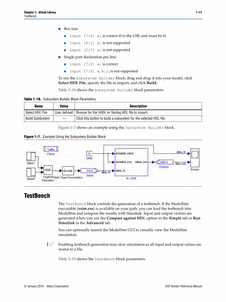
Subsystem BuilderThe Subsystem Builder block allows you to build black box subsystems that synthesize using user-supplied VHDL and simulate using non-DSP Builder Simulink blocks. This is an alternative to using HDL Import and can give better simulation speed. You can also use this block if HDL Import cannot be used due to unsupported megafunctions or LPMs.
The subsystem connects the inputs and outputs in the specified VHDL to HDL Input and HDL Output blocks and creates an HDL Entity block which you can modify if the clock and reset signals are not correctly identified.
The Subsystem Builder block automatically maps any input ports named simulink_clock in the VHDL entity section to the global VHDL clock signal, and maps any input ports named simulink_sclr in the VHDL entity section to the global VHDL synchronous clear signal.
The VHDL entity should be formatted according to the following guidelines:
■ The VHDL file should contain a single entity
■ Port direction: in or out
■ Port type: STD_LOGIC or STD_LOGIC_VECTOR
■ Bus size:
■ a(7 DOWNTO 0) is supported (0 is the LSB, and must be 0)
■ a(8 DOWNTO 1) is not supported
■ a(0 TO 7) is not supported
■ Single port declaration per line:
■ a:STD_LOGIC; is supported
■ a,b,c:STD_LOGIC; is not supported
The Verilog HDL module should be formatted according to the following guidelines:
■ The Verilog HDL file should contain a single module
■ Port direction: input or output
DSP Builder Reference Manual © January 2010 Altera Corporation
Chapter 1: AltLab Library 1–17TestBench
■ Bus size:
■ input [7:0] a; is correct (0 is the LSB, and must be 0)
■ input [8:1] a; is not supported
■ input [0:7] a; is not supported
■ Single port declaration per line:
■ input [7:0] a; is correct
■ input [7:0] a,b,c; is not supported
To use the Subsystem Builder block, drag and drop it into your model, click Select HDL File, specify the file to import, and click Build.
Table 1–18 shows the Subsystem Builder block parameters.
Figure 1–7 shows an example using the Subsystem Builder block.
TestBenchThe TestBench block controls the generation of a testbench. If the ModelSim executable (vsim.exe) is available on your path, you can load the testbench into ModelSim and compare the results with Simulink. Input and output vectors are generated when you use the Compare against HDL option in the Simple tab or Run Simulink in the Advanced tab.
You can optionally launch the ModelSim GUI to visually view the ModelSim simulation.
1 Enabling testbench generation may slow simulation as all input and output values are stored to a file.
Table 1–19 shows the TestBench block parameters.
Table 1–18. Subsystem Builder Block Parameters
Name Value Description
Select HDL File User defined Browse for the VHDL or Verilog HDL file to import.
Build SubSystem — Click this button to build a subsystem for the selected HDL file.
Figure 1–7. Example Using the Subsystem Builder Block
© January 2010 Altera Corporation DSP Builder Reference Manual

1–18 Chapter 1: AltLab LibraryVCD Sink
VCD SinkThe VCD Sink block is used to export Simulink signals to a third-party waveform viewer. When you run the simulation of your model, the VCD Sink block generates a value change dump (.vcd) file named <VCD Sink block name>.vcd which can be read by a third-party waveform viewer.
To use the VCD Sink block in your Simulink model, perform the following steps:
1. Add a VCD Sink block to your Simulink model.
2. Connect the simulink signals you want to display in a third-party waveform viewer to the VCD Sink block.
3. Run the Simulink simulation.
4. Read the VCD file in the third-party waveform viewer.
If you are using the ModelSim software to view waveforms, run the script <VCD Sink block path>_vcd.tcl where the path is the hierarchical path of the block in the Simulink model. That is: <model name>_<subsystem names>_<block name> each separated by underscore character.
This Tcl script converts VCD files to ModelSim waveform format (.wlf), starts the waveform viewer, and displays the signals. If you are using any other third-party viewer, load the VCD file directly into the viewer.
The VCD Sink block does not have any hardware representation and therefore does not appear in the VHDL RTL representation created by the Signal Compiler block.
Table 1–20 shows the parameters for the VCD Sink block.
Table 1–19. TestBench Block Parameters
Name Value Description
Enable Testbench generation On or Off Turn on to enable automatic testbench generation.
Compare against HDL — Click this button to generate HDL, run Simulink and compare the Simulink simulation results with ModelSim.
Generate HDL — Click this button to generate a VHDL testbench from the Simulink model.
Run Simulink — Re-run the Simulink simulation.
Run ModelSim — Load the testbench into the ModelSim simulator.
Launch GUI On or Off Turn on to launch the ModelSim graphical user interface.
Compare Results — Compare the Simulink and ModelSim results.
Mark ModelSim Unknowns (X’s) as
Error, Warning, Info
Choose whether ModelSim unknown values are displayed as error, warning or info messages. Errors are displayed in red, warnings in blue and info in green.
Maximum number of mismatches to display
>=0
Default = 10
Specify the maximum number of mismatches to display.
Table 1–20. VCD Sink Block Parameters
Name Value Description
Number of Inputs An integer greater than 0 Specify the number of input ports on the VCD Sink block.
DSP Builder Reference Manual © January 2010 Altera Corporation

Chapter 1: AltLab Library 1–19VCD Sink
Figure 1–8 shows an example of the VCD Sink block
Figure 1–8. Simulink Model Using the VCD Sink Block
© January 2010 Altera Corporation DSP Builder Reference Manual

1–20 Chapter 1: AltLab LibraryVCD Sink
DSP Builder Reference Manual © January 2010 Altera Corporation

© January 2010 Altera Corporation
2. Arithmetic Library
The Arithmetic library contains two’s complement signed arithmetic blocks such as multipliers and adders. Some blocks have a Use Dedicated Circuitry option, which implements functionality into dedicated hardware in the Altera FPGA devices (that is, in the dedicated DSP blocks of these devices).
f For more information about these device families, refer to the device documentation on the Altera literature website.
The Arithmetic library contains the following blocks:
■ Barrel Shifter
■ Bit Level Sum of Products
■ Comparator
■ Counter
■ Differentiator
■ Divider
■ DSP
■ Gain
■ Increment Decrement
■ Integrator
■ Magnitude
■ Multiplier
■ Multiply Accumulate
■ Multiply Add
■ Parallel Adder Subtractor
■ Pipelined Adder
■ Product
■ SOP Tap
■ Square Root
■ Sum of Products
DSP Builder Reference Manual
2–2 Chapter 2: Arithmetic LibraryBarrel Shifter
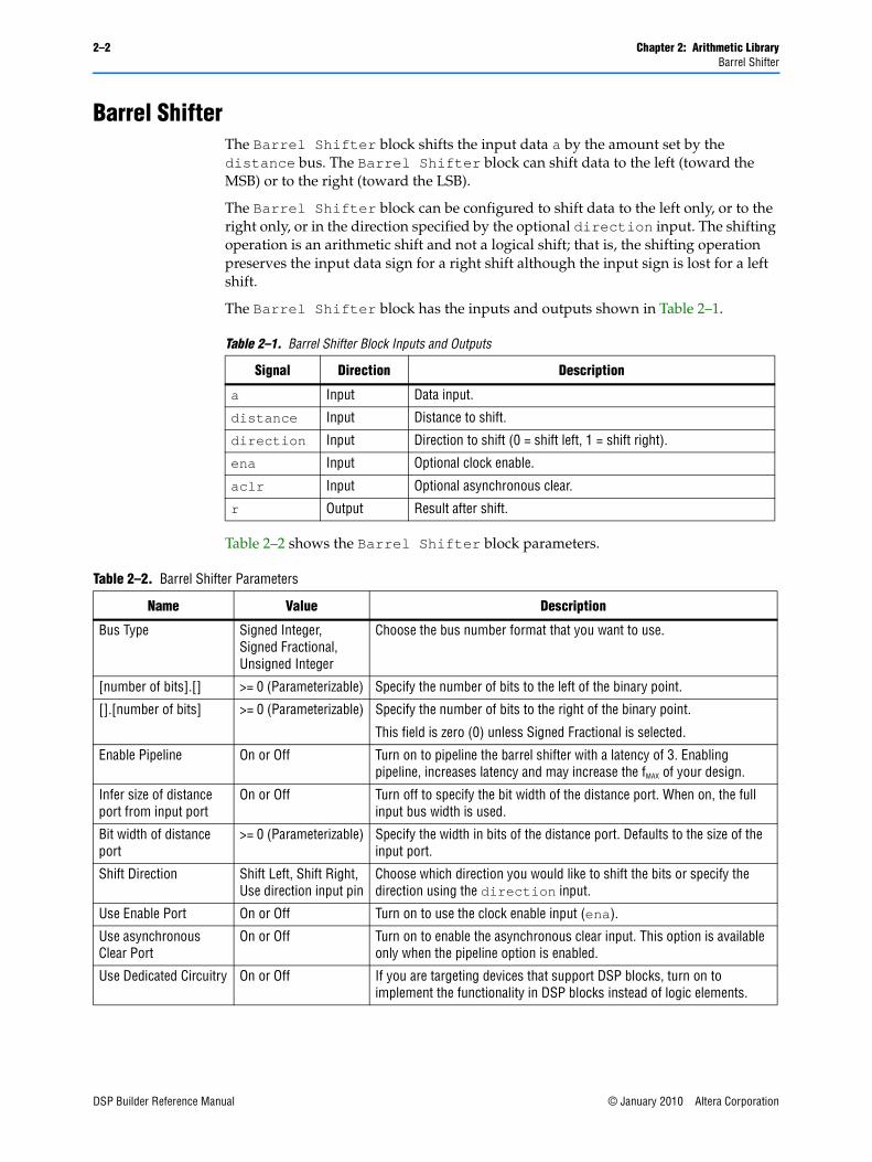
Barrel ShifterThe Barrel Shifter block shifts the input data a by the amount set by the distance bus. The Barrel Shifter block can shift data to the left (toward the MSB) or to the right (toward the LSB).
The Barrel Shifter block can be configured to shift data to the left only, or to the right only, or in the direction specified by the optional direction input. The shifting operation is an arithmetic shift and not a logical shift; that is, the shifting operation preserves the input data sign for a right shift although the input sign is lost for a left shift.
The Barrel Shifter block has the inputs and outputs shown in Table 2–1.
Table 2–2 shows the Barrel Shifter block parameters.
Table 2–1. Barrel Shifter Block Inputs and Outputs
Signal Direction Description
a Input Data input.
distance Input Distance to shift.
direction Input Direction to shift (0 = shift left, 1 = shift right).
ena Input Optional clock enable.
aclr Input Optional asynchronous clear.
r Output Result after shift.
Table 2–2. Barrel Shifter Parameters
Name Value Description
Bus Type Signed Integer, Signed Fractional, Unsigned Integer
Choose the bus number format that you want to use.
[number of bits].[] >= 0 (Parameterizable) Specify the number of bits to the left of the binary point.
[].[number of bits] >= 0 (Parameterizable) Specify the number of bits to the right of the binary point.
This field is zero (0) unless Signed Fractional is selected.
Enable Pipeline On or Off Turn on to pipeline the barrel shifter with a latency of 3. Enabling pipeline, increases latency and may increase the fMAX of your design.
Infer size of distance port from input port
On or Off Turn off to specify the bit width of the distance port. When on, the full input bus width is used.
Bit width of distance port
>= 0 (Parameterizable) Specify the width in bits of the distance port. Defaults to the size of the input port.
Shift Direction Shift Left, Shift Right, Use direction input pin
Choose which direction you would like to shift the bits or specify the direction using the direction input.
Use Enable Port On or Off Turn on to use the clock enable input (ena).
Use asynchronous Clear Port
On or Off Turn on to enable the asynchronous clear input. This option is available only when the pipeline option is enabled.
Use Dedicated Circuitry On or Off If you are targeting devices that support DSP blocks, turn on to implement the functionality in DSP blocks instead of logic elements.
DSP Builder Reference Manual © January 2010 Altera Corporation

Chapter 2: Arithmetic Library 2–3Bit Level Sum of Products
Table 2–3 shows the Barrel Shifter block I/O formats.
Figure 2–1 shows an example using the Barrel Shifter block.
Bit Level Sum of ProductsThe Bit Level Sum of Products block performs a sum of the multiplication of one-bit inputs by signed integer fixed coefficients.
The Bit Level Sum of Products block uses the equation:
q = a(0)C0 + ... + a(i)Ci + ... + a(n–1)Cn-1
where:
■ q is the output result
■ a(i) is the one-bit input data
■ Ci are the signed integer fixed coefficients
n is the number of coefficients in the range one to eight
The Bit Level Sum of Products block has the inputs and outputs shown in Table 2–4 on page 2–4.
Table 2–3. Barrel Shifter Block I/O Formats (Note 1)
I/O Simulink (2), (3) VHDL Type (4)
I I1[L1].[R1]
I2[L2].[R2]
I3[1]
I1: in STD_LOGIC_VECTOR({L1 + R1 - 1} DOWNTO 0)
I2: in STD_LOGIC_VECTOR({L2 + R2 - 1} DOWNTO 0)
I3: in STD_LOGIC
Explicit
Explicit
O O1[L1].[R1] O1: out STD_LOGIC_VECTOR({L1 + R1 - 1} DOWNTO 0 Explicit
Notes to Table 2–3:
(1) For signed integers and signed binary fractional numbers, the MSB is the sign bit.(2) [L] is the number of bits on the left side of the binary point; [R] is the number of bits on the right side of the binary point. For signed or unsigned
integers R = 0, that is, [L].[0]. For single bits, R = 0, that is, [1] is a single bit.(3) I1[L].[R] is an input port. O1[L].[R] is an output port.(4) Explicit means that the port bit width information is a block parameter. Implicit means that the port bit width information is set by the data path
bit width propagation mechanism. To specify the bus format of an implicit input port, use a Bus Conversion block to set the width.
Figure 2–1. Barrel Shifter Block Example
© January 2010 Altera Corporation DSP Builder Reference Manual

2–4 Chapter 2: Arithmetic LibraryBit Level Sum of Products
Table 2–5 shows the Bit Level Sum of Products block parameters.
Table 2–6 shows the Bit Level Sum of Products block I/O formats.
Table 2–4. Bit Level Sum of Products Block Inputs and Outputs
Signal Direction Description
a(0) to a(n–1) Input 1 to 8 ports corresponding to the signed integer fixed coefficient values specified in the block parameters.
ena Input Optional clock enable.
sclr Input Optional synchronous clear.
q Output Result.
Table 2–5. Bit Level Sum of Products Block Parameters
Name Value Description
Number of Coefficients 1–8 Choose the number of coefficients.
Coefficient Number of Bits
>= 1–51 (Parameterizable)
Specify the bit width as a signed integer. The bit width must be capable of being expressed as a double in MATLAB.
Signed Integer Fixed-Coefficient Values
User Defined (Parameterizable)
Specify the coefficient values for each port as a sequence of signed integers. the coefficient values must be capable of being expressed as a double in MATLAB. For example: [-21 2 13 5]
Register Inputs On or Off When on, a register is added on the input signal.
Use Enable Port On or Off Turn on to use the clock enable input (ena).
Use Synchronous Clear Port
On or Off Turn on to use the synchronous clear input (sclr).
Table 2–6. Bit Level Sum of Products Block I/O Formats (Note 1)
I/O Simulink (2), (3) VHDL Type (4)
I I1[1].[0]
...
Ii[1].[0]
...
In[1].[0]
I(n+1)[1]
I(n+2)[1]
I1: in STD_LOGIC
...
Ii: in STD_LOGIC
...
In: in STD_LOGIC
I(n+1): in STD_LOGIC
I(n+2): in STD_LOGIC
Explicit
O O1[L0].[0] O1: out STD_LOGIC_VECTOR({L0 - 1} DOWNTO 0 Explicit
Notes to Table 2–6:
(1) For signed integers and signed binary fractional numbers, the MSB is the sign bit.(2) [L] is the number of bits on the left side of the binary point; [R] is the number of bits on the right side of the binary point. For signed or unsigned
integers R = 0, that is, [L].[0]. For single bits, R = 0, that is, [1] is a single bit.(3) I1[L].[R] is an input port. O1[L].[R] is an output port.(4) Explicit means that the port bit width information is a block parameter. Implicit means that the port bit width information is set by the data path
bit width propagation mechanism. To specify the bus format of an implicit input port, use a Bus Conversion block to set the width.
DSP Builder Reference Manual © January 2010 Altera Corporation

Chapter 2: Arithmetic Library 2–5Comparator
Figure 2–2 shows an example using the Bit Level Sum of Products block.
ComparatorThe Comparator block compares two Simulink signals and returns a single bit. The Comparator block implicitly understands the input data type (for example, signed binary or unsigned integer) and produces a single-bit output.
The Comparator block has the inputs and outputs shown in Table 2–7.
Table 2–8 shows the Comparator block parameters.
Table 2–9 shows the Comparator block I/O formats.
Figure 2–2. Bit Level Sum of Products Block Example
Table 2–7. Comparator Block Inputs and Outputs
Signal Direction Description
a Input Operand a.
b Input Operand b.
<unnamed> Output Result.
Table 2–8. Comparator Block Parameters
Name Value Description
Operator a == b,a ~= b,a < b, a <= b,a >= b,a > b
Choose which operation you wish to perform on the two buses.
Table 2–9. Comparator Block I/O Formats (Part 1 of 2) (Note 1)
I/O Simulink (2), (3) VHDL Type (4)
I I1[L1].[R1]
I2[L2].[R2]
I1: in STD_LOGIC_VECTOR({L1 + R1 - 1} DOWNTO 0)
I1: in STD_LOGIC_VECTOR({L2 + R2 - 1} DOWNTO 0)
Implicit
Implicit
© January 2010 Altera Corporation DSP Builder Reference Manual

2–6 Chapter 2: Arithmetic LibraryCounter
Figure 2–3 shows an example using the Comparator block.
CounterThe Counter block is an up/down counter. For each cycle, the counter increments or decrements its output by the smallest amount that can be represented using the selected bus type.
The Counter block has the inputs and outputs shown in Table 2–10.
Table 2–11 shows the Counter block parameters.
O O1[1] O1: out STD_LOGIC Implicit
Notes to Table 2–9:
(1) For signed integers and signed binary fractional numbers, the MSB is the sign bit.(2) [L] is the number of bits on the left side of the binary point; [R] is the number of bits on the right side of the binary point. For signed or unsigned
integers R = 0, that is, [L].[0]. For single bits, R = 0, that is, [1] is a single bit.(3) I1[L].[R] is an input port. O1[L].[R] is an output port.(4) Explicit means that the port bit width information is a block parameter. Implicit means that the port bit width information is set by the data path
bit width propagation mechanism. To specify the bus format of an implicit input port, use a Bus Conversion block to set the width.
Table 2–9. Comparator Block I/O Formats (Part 2 of 2) (Note 1)
I/O Simulink (2), (3) VHDL Type (4)
Figure 2–3. Comparator Block Example
Table 2–10. Counter Block Inputs and Outputs
Signal Direction Description
data Input Optional parallel data input.
sload Input Optional synchronous load signal.
sset Input Optional synchronous set port. (Loads the specified constant value into the counter.)
updown Input Optional direction (1 = up; 0 = down).
clk_ena Input Optional clock enable. (Disables counting and sload, sset, sclr signals.)
ena Input Optional counter enable. (Disables counting but not sload, sset, and sclr signals.)
sclr Input Optional synchronous clear. (Loads zero into the counter.)
q Output Result.
Table 2–11. Counter Block Parameters (Part 1 of 2)
Name Value Description
Bus Type Signed Integer, Unsigned Integer, Signed Fractional
Choose the bus number format that you want to use for the counter.
[number of bits].[] >= 0 (Parameterizable) Specify the number of bits to the left of the binary point.
DSP Builder Reference Manual © January 2010 Altera Corporation

Chapter 2: Arithmetic Library 2–7Counter
Table 2–12 shows the Counter block I/O formats.
[].[number of bits] >= 0 (Parameterizable) Specify the number of bits to the right of the binary point. This field is ignored unless Signed Fractional selected.
Use Modulo On or Off Turn on to enable the Count Modulo parameter. This option is not available for bit widths greater than 31.
Count Modulo User defined (Parameterizable)
Specify the maximum count plus 1. This represents the number of unique states in the counter’s cycle.
Specify Clock On or Off Turn on to explicitly specify the clock name.
Clock User defined Specify the clock signal name.
Counter Direction Increment, Decrement, Use Direction Port (updown)
Choose which direction you would like to count or specify the direction using the direction input.
Use Synchronous Load Ports
On or Off Turn on to use the synchronous load inputs (data, sload).
Use Synchronous Set Port
On or Off Turn on to use the synchronous set input (sset). This option is not available for bit widths greater than 31.
Set Value User defined Specify the constant value loaded when the sset input is used. This value must be less than the Count Modulo value (if used).
Use Clock Enable Port On or Off Turn on to use the clock enable input (clk_ena).
Use Counter Enable Port
On or Off Turn on to use the counter enable input (ena).
Use Synchronous Clear Port
On or Off Turn on to use the synchronous clear input (sclr).
Table 2–11. Counter Block Parameters (Part 2 of 2)
Name Value Description
Table 2–12. Counter Block I/O Formats (Note 1)
I/O Simulink (2), (3) VHDL Type (4)
I I1[L].[R]]
I2[1]
I3[1]
I4[1]
I5[1]
I6[1]
I1: in STD_LOGIC_VECTOR({L + R - 1} DOWNTO 0)
I2: in STD_LOGIC
I3: in STD_LOGIC
I4: in STD_LOGIC
I5: in STD_LOGIC
I6: in STD_LOGIC
Explicit
O O1[L].[R] O1: out STD_LOGIC_VECTOR({L + R - 1} DOWNTO 0) Explicit
Notes to Table 2–12:
(1) For signed integers and signed binary fractional numbers, the MSB is the sign bit.(2) [L] is the number of bits on the left side of the binary point; [R] is the number of bits on the right side of the binary point. For signed or unsigned
integers R = 0, that is, [L].[0]. For single bits, R = 0, that is, [1] is a single bit.(3) I1[L].[R] is an input port. O1[L].[R] is an output port.(4) Explicit means that the port bit width information is a block parameter. Implicit means that the port bit width information is set by the data path
bit width propagation mechanism. To specify the bus format of an implicit input port, use a Bus Conversion block to set the width.
© January 2010 Altera Corporation DSP Builder Reference Manual

2–8 Chapter 2: Arithmetic LibraryDifferentiator
DifferentiatorThe Differentiator block is a signed integer differentiator with the equation:
q(n) = d(n) - d(n-D)
where D is the delay parameter.
You can use this block for DSP functions such as CIC filters.
The transfer function implemented by the Differentiator block is described by the equation 1-z-D.
The Differentiator block has the inputs and outputs shown in Table 2–13.
Table 2–14 shows the Differentiator block parameters.
Table 2–15 shows the Differentiator block I/O formats.
Table 2–13. Differentiator Block Inputs and Outputs
Signal Direction Description
d Input Data input.
ena Input Optional clock enable.
sclr Input Optional synchronous clear.
q Output Result.
Table 2–14. Differentiator Block Parameters
Name Value Description
Number of Bits >= 1
(Parameterizable)
Specify the number of bits.
Depth Any positive number (Parameterizable)
Specify the depth of the differentiator register.
Use Enable Port On or Off Turn on to use the clock enable input (ena).
Use Synchronous Clear Port On or Off Turn on to use the synchronous clear input (sclr).
Table 2–15. Differentiator Block I/O Formats (Note 1)
I/O Simulink (2), (3) VHDL Type (4)
I I1[L1].[0]
I2[1]
I3[1]
I1: in STD_LOGIC_VECTOR({L1 - 1} DOWNTO 0)
I2: in STD_LOGIC
I3: in STD_LOGIC
Explicit
O O1[L1].[0] O1: out STD_LOGIC_VECTOR({L1 - 1} DOWNTO 0) Explicit
Notes to Table 2–15:
(1) For signed integers and signed binary fractional numbers, the MSB is the sign bit.(2) [L] is the number of bits on the left side of the binary point; [R] is the number of bits on the right side of the binary point. For signed or unsigned
integers R = 0, that is, [L].[0]. For single bits, R = 0, that is, [1] is a single bit.(3) I1[L].[R] is an input port. O1[L].[R] is an output port.(4) Explicit means that the port bit width information is a block parameter. Implicit means that the port bit width information is set by the data path
bit width propagation mechanism. To specify the bus format of an implicit input port, use a Bus Conversion block to set the width.
DSP Builder Reference Manual © January 2010 Altera Corporation

Chapter 2: Arithmetic Library 2–9Divider
Figure 2–4 shows an example using the Differentiator block.
DividerThe Divider block takes a numerator and a denominator and returns the quotient and a remainder using the equation:
a = b × q + r.
q and r are undefined if b is zero.
1 Dividing a maximally negative number by a minimally negative one (-1 if using signed integers), outputs a truncated answer.
The numerator and denominator inputs can have different widths but are converted to the specified bit width.
The Divider block has the inputs and outputs shown in Table 2–16.
Table 2–17 shows the Divider block parameters.
Figure 2–4. Differentiator Block Example
Table 2–16. Divider Block Inputs and Outputs
Signal Direction Description
a Input Numerator.
b Input Denominator.
ena Input Optional clock enable.
aclr Input Optional asynchronous clear.
q Output Quotient.
r Output Remainder.
Table 2–17. Divider Block Parameters (Part 1 of 2)
Name Value Description
Bus Type Signed Integer, Signed Fractional, Unsigned Integer
Choose the bus number format that you want to use for the divider.
[number of bits].[] >= 0 (Parameterizable)
Specify the number of bits to the left of the binary point.
© January 2010 Altera Corporation DSP Builder Reference Manual

2–10 Chapter 2: Arithmetic LibraryDSP
Table 2–18 shows the Divider block I/O formats.
Figure 2–5 shows an example using the Divider block.
DSPThe DSP block consists of one to four multipliers feeding a parallel adder. It is equivalent to the Multiply Add block but exposes extra features (including chaining) that are available only on Stratix IV and Stratix III DSP blocks.
The DSP block accepts one to four pairs of multiplier inputs a and b. The operands in each pair are multiplied together. The second and fourth multiplier outputs can optionally be added or subtracted from the total.
[].[number of bits] >= 0 (Parameterizable)
Specify the number of bits to the right of the binary point. This option applies only to signed fractional formats.
Number of Pipeline Stages
0 to number of bits (Parameterizable)
When non-zero, adds pipeline stages to increase the data throughput. The clock enable and asynchronous clear ports are available only if the block is registered (that is, if the number of pipeline stages is greater than or equal to 1).
Use Enable Port On or Off Turn on to use the clock enable input (ena).
Use Asynchronous Clear Port
On or Off Turn on to use the asynchronous clear input (aclr).
Table 2–17. Divider Block Parameters (Part 2 of 2)
Name Value Description
Table 2–18. Divider Block I/O Formats (Note 1)
I/O Simulink (2), (3) VHDL Type (4)
I I1[L].[R]
I2[L].[R]
I3[1]
I4[1]
I1: in STD_LOGIC_VECTOR({L + R - 1} DOWNTO 0)
I2: in STD_LOGIC_VECTOR({L + R - 1} DOWNTO 0)
I3: in STD_LOGIC
I4: in STD_LOGIC
Explicit
Explicit
O O1[L].[R]
O2[L].[R]
O1: out STD_LOGIC_VECTOR({L + R - 1} DOWNTO 0)
O2: out STD_LOGIC_VECTOR({L + R - 1} DOWNTO 0)
Explicit
Explicit
Notes to Table 2–18:
(1) For signed integers and signed binary fractional numbers, the MSB is the sign bit.(2) [L] is the number of bits on the left side of the binary point; [R] is the number of bits on the right side of the binary point. For signed or unsigned
integers R = 0, that is, [L].[0]. For single bits, R = 0, that is, [1] is a single bit.(3) I1[L].[R] is an input port. O1[L].[R] is an output port.(4) Explicit means that the port bit width information is a block parameter. Implicit means that the port bit width information is set by the data path
bit width propagation mechanism. To specify the bus format of an implicit input port, use a Bus Conversion block to set the width.
Figure 2–5. Divider Block Example
DSP Builder Reference Manual © January 2010 Altera Corporation

Chapter 2: Arithmetic Library 2–11DSP
The block function can be expressed by the equation:
res = a0×b0 ± a1×b1 [+ a2×b2 [± a3×b3]] [+ chainin]
If there are four multipliers and the input bit widths are both less than or equal to 18, you can optionally enable a chainout adder output (chainout) instead of the normal output (res).
If there are four multipliers and the input bit widths are both equal to 18, you can enable a chainout adder input (chainin). This chainin port can only be driven from the chainout output of a DSP block at the preceding stage.
Other features include:
■ Parameterizable input and output data widths
■ Optional asynchronous clear and clock enable inputs
■ Optional accumulator synchronous load input
■ Optional shiftin instead of an a input
■ Optional shift out from the a input of the last multiplier
■ Optional saturation overflow outputs
■ Optional registers to pipeline the adder and chainout adder
■ Optional accumulator mode
f For more information about multiplier/adder operations, refer to the altmult_add Megafunction User Guide.
The DSP block has the inputs and outputs shown in Table 2–19.
Table 2–19. DSP Block Inputs and Outputs
Signal Direction Description
a0—a3 Input Operand a.
b0—b3 Input Operand b.
ena Input Optional clock enable.
chainin Input Optional input bus from the preceding stage. (Note 1)
zero_chainout Input Optional reset to zero for the chainout value.
aclr Input Optional asynchronous clear.
accum_sload Input Optional accumulator synchronous load input.
res Output Result.
shiftouta Output Optional shift out from A input of last multiplier.
overflow Output Optional saturation overflow output.
chainout Output Optional chainout output. (Replaces the res output when enabled.)
Note to Table 2–19:
(1) You can use the chainin port to feed the adder result (chainout) from a previous stage. It should not be used for any other signal.
© January 2010 Altera Corporation DSP Builder Reference Manual

2–12 Chapter 2: Arithmetic LibraryDSP
Figure 2–6 shows a basic multiplier/adder with two inputs whose product are subtracted.
Figure 2–7 shows a 4-input multiplier/adder with shiftin inputs, registered outputs, rounding and saturation enabled, a chainout adder and saturation overflow outputs.
Figure 2–6. Basic 2-Input Multiplier/Adder
Figure 2–7. 4-Input Multiplier/Adder with Chainout Adder
DSP Builder Reference Manual © January 2010 Altera Corporation

Chapter 2: Arithmetic Library 2–13DSP
Table 2–20 shows the DSP block parameters.
Table 2–20. DSP Block Parameters (Part 1 of 2)
Name Value Description
Number of Multipliers 1, 2, 3, 4 Choose how many multipliers you want to feed the adder.
Bus Type Signed Integer, Unsigned Integer, Signed Fractional
Choose the number format you wish to use for the bus.
a Inputs [number of bits].[] >= 0 (Parameterizable)
Specify the number of data a input bits to the left of the binary point, including the sign bit.
a Inputs [].[number of bits] >= 0 (Parameterizable)
Specify the number of data a input bits to the right of the binary point. This option applies only to signed fractional formats.
b Inputs [number of bits].[] >= 0 (Parameterizable)
Specify the number of data b input bits to the left of the binary point, including the sign bit.
b Inputs [].[number of bits] >= 0 (Parameterizable)
Specify the number of data b input bits to the right of the binary point. This option applies only to signed fractional formats.
Connect Multiplier Input a to shiftin
On or Off Turn on to connect the multiplier input a to shiftin from the previous multiplier. (Separate inputs are used for each multiplier.)
Use Shiftout from a Input of Last Multiplier
On or Off Turn on to create a shiftouta output from the a input of the last multiplier.
Output Operation on First Multiplier Pair
ADD, SUB Choose whether to add or subtract the product of the first multiplier pair.
Output Operation on Second Multiplier Pair
ADD, SUB Choose whether to add or subtract the product of the second multiplier pair.
Enable Accumulator Mode On or Off Turn on to enable accumulator mode. When this option is on, you can choose the accumulator direction and choose whether to use the optional accum_sload input.
Accumulator Direction ADD, SUB Choose whether to add or subtract values in the accumulator.
Use Accumulator Synchronous Load Input
On or Off Turn on to use the optional accum_sload input.
Use Chainout Adder Input (chainin)
On or Off Turn on to use the chainin input for the chainout adder to add the result from a previous stage. This option is available only if the input bit widths are less than or equal to 18 and the number of multipliers is 4.
Use Chainout Adder Output (chainout)
On or Off Turn on to use the chainout output from the chainout adder output instead of the res output. This option is available only if the input bit widths are less than or equal to 18 and the number of multipliers is 4.
Use Zero Chainout Input On or Off Turn on to use the zero_chainout input which dynamically sets the chainout value to zero.
Full Resolution for Output Result
On or Off When on, the multiplier output bit width is full resolution. When off, you can specify a different output width. Rounding and saturation are available for certain input/output type combinations.
Output [number of bits].[] >= 0 (Parameterizable)
Specify the number of data output bits to the left of the binary point, including the sign bit.
Output [].[number of bits] >= 0 (Parameterizable)
Specify the number of data output bits to the right of the binary point. This option applies only to signed fractional formats.
Output Rounding Operation Type
None (truncate), Nearest Integer, Nearest Even
You can choose whether to disable rounding (truncate), round to the nearest integer or round to the nearest even.
© January 2010 Altera Corporation DSP Builder Reference Manual

2–14 Chapter 2: Arithmetic LibraryDSP
1 Compilation in the Quartus II software requires that the input bit widths are 18 bits when you are using the chainout adder input, output rounding with an output LSB in the range 6 to 21, or output saturation with an output MSB in the range 28 to 43.
Table 2–21 shows the DSP block I/O formats.
Output Saturation Operation Type
None (wrap), Symmetric, Asymmetric
You can choose whether to disable (wrap), or enable saturation. Symmetric saturation specifies that the absolute value of the maximum negative number is equal to the maximum positive number. Asymmetric saturation specifies that the absolute value of the maximum negative number is 1 greater than the maximum positive number. Do not enable rounding unless you have enabled saturation.
Use Output Overflow Port On or Off Turn on to use the overflow output for the saturation unit.
Register Data Inputs to the Multiplier(s)
On or Off Turn on to create registers at the data inputs to the multiplier. (Always on if in shiftin mode.)
Register Output of the Multiplier
On or Off Turn on to create a register at the data output from the multiplier.
Register Output of the Adder
On or Off Turn on to create a register at the output of the adder. (Always on if accumulator mode is enabled.)
Register Chainout Adder On or Off Turn on to create a register at the output of the chainout adder (if it is used).
Register Shiftout On or Off Registers the shiftouta output (if it is used).
Use Enable Port On or Off Turn on to use the clock enable input (ena) if using registers.
Use User Asynchronous Clear Port
On or Off Turn on to use the asynchronous clear input (aclr) if using registers.
Table 2–20. DSP Block Parameters (Part 2 of 2)
Name Value Description
Table 2–21. DSP Block I/O Formats (Note 1)
I/O Simulink (2), (3) VHDLType (4)
I I1[L1].[R1]
….
In[L1].[R1]
I(n+1)[1]
I(n+2)[1]
where 3 < n < 9
I1: in STD_LOGIC_VECTOR({L1 + R1 - 1} DOWNTO 0)
….
In: in STD_LOGIC_VECTOR({L1 + R1 - 1} DOWNTO 0)
I(n+1): in STD_LOGIC
I(n+2): in STD_LOGIC
where 3 < n < 9
Explicit
...
Explicit
O O12 x [L1]+ ceil(log2(n)).2 x [R1] O1: out STD_LOGIC_VECTOR({(2 x L1) + ceil(log2(n)) + (2 x R1) - 1} DOWNTO 0) Implicit
Notes to Table 2–21:
(1) For signed integers and signed binary fractional numbers, the MSB is the sign bit.(2) [L] is the number of bits on the left side of the binary point; [R] is the number of bits on the right side of the binary point. For signed or unsigned
integers R = 0, that is, [L].[0]. For single bits, R = 0, that is, [1] is a single bit.(3) I1[L].[R] is an input port. O1[L].[R] is an output port.(4) Explicit means that the port bit width information is a block parameter. Implicit means that the port bit width information is set by the data path
bit width propagation mechanism. To specify the bus format of an implicit input port, use a Bus Conversion block to set the width.
DSP Builder Reference Manual © January 2010 Altera Corporation

Chapter 2: Arithmetic Library 2–15Gain
Figure 2–8 shows an example of a basic lo-pass filter using two DSP blocks.
GainThe Gain block generates its output by multiplying the signal input by a specified gain factor. You must enter the gain as a numeric value in the Gain block parameter field. The gain factor must be a scalar.
1 The Simulink software also provides a Gain block. If you use the Simulink Gain block in your model, you can use it only for simulation; Signal Compiler cannot convert it to HDL.
The Gain block has the inputs and outputs shown in Table 2–22.
Figure 2–8. DSP Block Example
Table 2–22. Gain Block Inputs and Outputs
Signal Direction Description
d Input Data input.
ena Input Optional clock enable.
aclr Input Optional asynchronous clear.
<unnamed> Output Result.
© January 2010 Altera Corporation DSP Builder Reference Manual

2–16 Chapter 2: Arithmetic LibraryGain
Table 2–23 shows the Gain block parameters.
Table 2–24 shows the Gain block I/O formats.
Table 2–23. Gain Block Parameters
Name Value Description
Gain Value User Defined Specify the gain value you want to use as a decimal number (or an expression that evaluates to a decimal number). The gain is masked to the number format (bus type) you select.
Map Gain Value to Bus Type Signed Integer, Signed Fractional, Unsigned Integer
Choose the bus number format you want to use for the gain value.
[Gain value number of bits].[] >= 0 (Parameterizable)
Specify the number of bits to the left of the binary point, including the sign bit.
[].[Gain value number of bits] >= 0 (Parameterizable)
Specify the number of bits to the right of the binary point. This option applies only to signed fractional formats.
Number of Pipeline Stages >= 0 (Parameterizable)
Choose the number of pipeline delay stages. The Clock Phase Selection and Optional Ports options are available only if the block is registered (that is, if the number of pipeline stages is greater than or equal to 1).
Clock Phase Selection User Defined Specify the phase selection with a binary string, where a 1 indicates the phase in which the block is enabled. For example:
1—The block is always enabled and captures all data passing through the block (sampled at the rate 1).
10—The block is enabled every other phase and every other data (sampled at the rate 1) passes through.
0100—The block is enabled on the second phase of and only the second data of (sampled at the rate 1) passes through. That is, the data on phases 1, 3, and 4 do not pass through the block.
Use Enable Port On or Off Turn on to use the clock enable input (ena).
Use Asynchronous Clear Port On or Off Turn on to use the asynchronous clear input (aclr).
Use LPM On or Off This parameter is used for synthesis.
When on, the Gain block is mapped to the LPM_MULT library of parameterized modules (LPM) function and the VHDL synthesis tool uses the Altera LPM_MULT implementation.
Table 2–24. Gain Block I/O Formats (Part 1 of 2) (Note 1)
I/O Simulink (2), (3) VHDL Type
I I1[L1].[R1]
I2[1]
I3[1]
I1: in STD_LOGIC_VECTOR({L1 + R1 - 1} DOWNTO 0)
I2: in STD_LOGIC
I3: in STD_LOGIC
Implicit (4)
DSP Builder Reference Manual © January 2010 Altera Corporation

Chapter 2: Arithmetic Library 2–17Increment Decrement
Figure 2–9 shows an example using the Gain block.
Increment DecrementThe Increment Decrement block increments or decrements a value in time. The output can be a signed integer, unsigned integer, or signed binary fractional number. For all number formats, the counting sequence increases or decreases by the smallest representable value; for integer types, the value always changes by 1.
The Increment Decrement block has the inputs and outputs shown in Table 2–25.
Table 2–26 shows the Increment Decrement block parameters.
O O1[L1 + LK].2*max(R1,RK)] (5) O1: out STD_LOGIC_VECTOR({L1+LK+2*max(R1,RK)-1} DOWNTO 0) Implicit
Notes to Table 2–24:
(1) For signed integers and signed binary fractional numbers, the MSB is the sign bit.(2) [L] is the number of bits on the left side of the binary point; [R] is the number of bits on the right side of the binary point. For signed or unsigned
integers R = 0, that is, [L].[0]. For single bits, R = 0, that is, [1] is a single bit.(3) I1[L].[R] is an input port. O1[L].[R] is an output port.(4) Explicit means that the port bit width information is a block parameter. Implicit means that the port bit width information is set by the data path
bit width propagation mechanism. To specify the bus format of an implicit input port, use a Bus Conversion block to set the width.(5) K is the gain constant with the format K[LK].[RK]
Table 2–24. Gain Block I/O Formats (Part 2 of 2) (Note 1)
I/O Simulink (2), (3) VHDL Type
Figure 2–9. Gain Block Example
Table 2–25. Increment Decrement Block Inputs and Outputs
Signal Direction Description
ena Input Optional clock enable.
sclr Input Optional synchronous clear.
c Output Result.
Table 2–26. Increment Decrement Block Parameters (Part 1 of 2)
Name Value Description
Bus Type Signed Integer, Signed Fractional, Unsigned Integer
Choose the number format you wish to use for the bus.
<number of bits>.[] >= 0 (Parameterizable)
Select the number of bits to the left of the binary point, including the sign bit.
[].<number of bits> >= 0 (Parameterizable)
Select the number of bits to the right of the binary point. This option applies only to signed fractional formats.
© January 2010 Altera Corporation DSP Builder Reference Manual

2–18 Chapter 2: Arithmetic LibraryIncrement Decrement
Table 2–27 shows the Increment Decrement block I/O formats.
Figure 2–10 shows an example using the Increment Decrement block.
Direction Increment, Decrement
Choose whether you wish to count up or down.
Starting Value User Defined (Parameterizable)
Enter the value with which to begin counting. This will be the initial output value of the block after a reset.
Clock Phase Selection
User Defined Specify the phase selection with a binary string, where a 1 indicates the phase in which the block is enabled. For example:
1—The block is always enabled and captures all data passing through the block (sampled at the rate 1).
10—The block is enabled every other phase and every other data (sampled at the rate 1) passes through.
0100—The block is enabled on the second phase of and only the second data of (sampled at the rate 1) passes through. That is, the data on phases 1, 3, and 4 do not pass through the block.
Specify Clock On or Off Turn on to explicitly specify the clock name.
Clock User defined Specify the clock signal name.
Use Enable Port On or Off Turn on if you would like to use the clock enable input (ena).
Use Synchronous Clear Port
On or Off Turn on if you would like to use the synchronous clear input (sclr).
Table 2–26. Increment Decrement Block Parameters (Part 2 of 2)
Name Value Description
Table 2–27. Increment Decrement Block I/O Formats (Note 1)
I/O Simulink (2), (3) VHDL Type (4)
I I1[1]
I2[1]
I1: in STD_LOGIC
I2: in STD_LOGIC
O O1[LP].[RP] O1: out STD_LOGIC_VECTOR({LP + RP - 1} DOWNTO 0) Explicit
Notes to Table 2–27:
(1) For signed integers and signed binary fractional numbers, the MSB is the sign bit.(2) [L] is the number of bits on the left side of the binary point; [R] is the number of bits on the right side of the binary point. For signed or unsigned
integers R = 0, that is, [L].[0]. For single bits, R = 0, that is, [1] is a single bit.(3) I1[L].[R] is an input port. O1[L].[R] is an output port.(4) Explicit means that the port bit width information is a block parameter. Implicit means that the port bit width information is set by the data path
bit width propagation mechanism. To specify the bus format of an implicit input port, use a Bus Conversion block to set the width.
Figure 2–10. Increment Decrement Block Example
DSP Builder Reference Manual © January 2010 Altera Corporation

Chapter 2: Arithmetic Library 2–19Integrator
IntegratorThe Integrator block is a signed integer integrator with the equation:
q(n+D) = q(n) + d(n)
where D is the delay parameter.
You can use this block for DSP functions such as CIC filters.
The transfer function implemented by the Integrator block is described by the equation z-D/(1-z-D). This behavior of this transfer function is slightly different from the more typical 1/(1-z-D).
Figure 2–11 shows the block diagrams for these functions.
The magnitude response of these two functions is the same although their phase response is different. For the typical integrator function, 1/(1-z-D), there would be an impulse on the output at time = 0, whereas the output is delayed by a factor of D for the z-D/(1-z-D) function used by the DSP Builder integrator.
This behavior effectively registers the output and gives a better Fmax performance compared to the typical function where if you chained a row of n integrators together, it would be equivalent to n unregistered adder blocks in a row, and would be slow in hardware.
The Integrator block has the inputs and outputs shown in Table 2–28.
Figure 2–11. Integrator Transfer Functions
Table 2–28. Integrator Block Inputs and Outputs
Signal Direction Description
d Input Data input.
ena Input Optional clock enable.
sclr Input Optional synchronous clear.
q Output Result.
© January 2010 Altera Corporation DSP Builder Reference Manual

2–20 Chapter 2: Arithmetic LibraryIntegrator
Table 2–29 shows the Integrator block parameters.
Table 2–30 shows the Integrator block I/O formats.
Figure 2–12 shows an example of the Integrator Block.
Table 2–29. Integrator Block Parameters
Name Value Description
Number of Bits >= 1 (Parameterizable)
Specify the number of bits.
Depth A positive number (Parameterizable)
Specify the depth of the integrator register.
Use Enable Port On or Off Turn on to use the clock enable input (ena).
Use Synchronous Clear Port On or Off Turn on to use the synchronous clear input (sclr).
Table 2–30. Integrator Block I/O Formats (Note 1)
I/O Simulink (2), (3) VHDL Type (4)
I I1[L1].[0]
I2[1]
I3[1]
I1: in STD_LOGIC_VECTOR({L1 - 1} DOWNTO 0)
I2: STD_LOGIC
I3: STD_LOGIC
Explicit
O O1[L1].[0] O1: out STD_LOGIC_VECTOR({L1 - 1} DOWNTO 0) Explicit
Notes to Table 2–30:
(1) For signed integers and signed binary fractional numbers, the MSB is the sign bit.(2) [L] is the number of bits on the left side of the binary point; [R] is the number of bits on the right side of the binary point. For signed or unsigned
integers R = 0, that is, [L].[0]. For single bits, R = 0, that is, [1] is a single bit.(3) I1[L].[R] is an input port. O1[L].[R] is an output port.(4) Explicit means that the port bit width information is a block parameter. Implicit means that the port bit width information is set by the data path
bit width propagation mechanism. To specify the bus format of an implicit input port, use a Bus Conversion block to set the width.
Figure 2–12. Integrator Block Example Design
DSP Builder Reference Manual © January 2010 Altera Corporation

Chapter 2: Arithmetic Library 2–21Magnitude
Magnitude The scalar Magnitude block returns the absolute value of the incoming signed binary fractional bus.
The Magnitude block has no parameters.
Table 2–31 shows the Magnitude block I/O formats.
Figure 2–13 shows an example using the Magnitude block.
MultiplierThe Multiplier block supports two scalar inputs (no multi-dimensional Simulink signals). Operand a is multiplied by operand b and the result r output as shown by the following equation:
r = a × b
The differences between the Multiplier block and the Product block are:
■ The Product block supports clock phase selection while the Multiplier block does not.
■ The Product block uses implicit input port data widths that are inherited from the signals’ sources, whereas the Multiplier block uses explicit input port data widths that must be specified as parameters.
■ The Product block allows you to choose whether to use the LPM multiplier megafunction, whereas the Multiplier block always uses the LPM.
Table 2–31. Magnitude Block I/O Formats (Note 1)
I/O Simulink (2), (3) VHDL Type (4)
I I1[L1].[R1] I1: in STD_LOGIC_VECTOR({L1 + R1 - 1} DOWNTO 0) Implicit
O O1[L1].[R1] O1: out STD_LOGIC_VECTOR({L1 + R1 - 1} DOWNTO 0) Implicit
Notes to Table 2–31:
(1) For signed integers and signed binary fractional numbers, the MSB is the sign bit.(2) [L] is the number of bits on the left side of the binary point; [R] is the number of bits on the right side of the binary point. For signed or unsigned
integers R = 0, that is, [L].[0]. For single bits, R = 0, that is, [1] is a single bit.(3) I1[L].[R] is an input port. O1[L].[R] is an output port.(4) Explicit means that the port bit width information is a block parameter. Implicit means that the port bit width information is set by the data path
bit width propagation mechanism. To specify the bus format of an implicit input port, use a Bus Conversion block to set the width.
Figure 2–13. Magnitude Block Example
© January 2010 Altera Corporation DSP Builder Reference Manual

2–22 Chapter 2: Arithmetic LibraryMultiplier
The Multiplier block has the inputs and outputs shown in Table 2–32.
Table 2–33 lists the parameters for the Multiplier block.
Table 2–32. Multiplier Block Inputs and Outputs
Signal Direction Description
a Input Operand a.
b Input Operand b.
ena Input Optional clock enable.
aclr Input Optional asynchronous clear.
r Output Result r.
Table 2–33. Multiplier Block Parameters (Part 1 of 2)
Name Value Description
Bus Type Signed Integer, Signed Fractional, Unsigned Integer
Choose the bus number format to use for the Multiplier block.
Input [number of bits].[] >= 0 (Parameterizable)
Specify the number of bits to the left of the binary point for input a (or both input signals if set to have the same width).
Input [].[number of bits] >= 0 (Parameterizable)
Specify the number of bits to the right of the binary point for input a (or both input signals if set to have the same width). This option applies only to signed fractional formats.
Number of Pipeline Stages >= 0 (Parameterizable)
Choose the number of pipeline stages. The ena and aclr ports are available only if the block is registered (that is, if the number of pipeline stages is greater than or equal to 1).
Both Inputs Have Same Bit Width
On or Off Turn on if you would like input a and input b to have the same bit width. When off, additional fields are available to specify the number of bits to the left and right of the binary point for input b.
Input b [number of bits].[] >= 0 (Parameterizable)
Specify the number of bits to the left of the binary point for input b.
Input b [].[number of bits] >= 0 (Parameterizable)
Specify the number of bits to the right of the binary point for input b. This option applies only to signed fractional formats.
Full Resolution for Output Result
On or Off When on, the multiplier output bit width is full resolution. When off, you can specify the number of bits used for the output.
Output MSB >= 0 (Parameterizable)
Specify the number of most significant bits used in the output for an integer bus.
Output LSB >= 0 (Parameterizable)
Specify the number of least significant bits used in the output for an integer bus.
Output [number of bits].[] >= 0 (Parameterizable)
Specify the number of bits to the left of the binary point for the output r. This option applies only to signed fractional formats.
Output [].[number of bits] >= 0 (Parameterizable)
Specify the number of bits to the left of the binary point for the output r. This option applies only to signed fractional formats.
Use Dedicated Circuitry AUTO, YES, NO Choose whether to use dedicated multiplier circuitry (if supported by your target device). A value of AUTO means that the Quartus II software chooses whether to use the dedicated multiplier circuitry based on the width of the multiplier.
DSP Builder Reference Manual © January 2010 Altera Corporation

Chapter 2: Arithmetic Library 2–23Multiplier
Table 2–34 shows the Multiplier block I/O formats.
Figure 2–14 shows an example using the Multiplier block.
f For more information about multiplier operations, refer to the Multiplier Megafunction User Guide.
Use Enable Port On or Off Turn on to use the clock enable input (ena).
Use Asynchronous Clear Port
On or Off Turn on to use the synchronous clear input (aclr).
Table 2–33. Multiplier Block Parameters (Part 2 of 2)
Name Value Description
Table 2–34. Multiplier Block Input/Output Ports (Note 1)
I/O Simulink (2), (3) VHDL Type (4)
I I1[L].[R]
I2[L].[R]
I3[1]
I4[1]
I1: in STD_LOGIC_VECTOR({L + R - 1} DOWNTO 0)
I2: in STD_LOGIC_VECTOR({L + R - 1} DOWNTO 0)
I3: STD_LOGIC
I4: STD_LOGIC
Explicit
Explicit
O O1[Lo].[Ro]
O2[Lo].[Ro]
O1: out STD_LOGIC_VECTOR({Lo + Ro - 1} DOWNTO 0)
O2: out STD_LOGIC_VECTOR({Lo + Ro - 1} DOWNTO 0)
Explicit
Explicit
Notes to Table 2–34:
(1) For signed integers and signed binary fractional numbers, the MSB is the sign bit.(2) [L] is the number of bits on the left side of the binary point; [R] is the number of bits on the right side of the binary point. For signed or unsigned
integers R = 0, that is, [L].[0]. For single bits, R = 0, that is, [1] is a single bit.(3) I1[L].[R] is an input port. O1[L].[R] is an output port.(4) Explicit means that the port bit width information is a block parameter. Implicit means that the port bit width information is set by the data path
bit width propagation mechanism. To specify the bus format of an implicit input port, use a Bus Conversion block to set the width.
Figure 2–14. Multiplier Block Example
© January 2010 Altera Corporation DSP Builder Reference Manual

2–24 Chapter 2: Arithmetic LibraryMultiply Accumulate
Multiply AccumulateThe Multiply Accumulate block consists of a single multiplier feeding an accumulator which performs the calculation y += a × b.
The input can be in signed integer, unsigned integer, or signed binary fractional formats.
The Multiply Accumulate block has the inputs and outputs shown in Table 2–35.
Table 2–36 shows the Multiply Accumulate block parameters.
Table 2–35. Multiply Accumulate Block Inputs and Outputs
Signal Direction Description
a Input Operand A.
b Input Operand B.
sload Input Synchronous load signal.
addsub Input Optional accumulator direction (1= add, 0 = subtract).
ena Input Optional clock enable.
aclr Input Optional asynchronous clear.
y Output Result.
Table 2–36. Multiply Accumulate Block Parameters (Part 1 of 2)
Name Value Description
Bus Type Signed Integer, Signed Fractional, Unsigned Integer
Choose the number format you wish to use for the bus.
Input A [number of bits].[] >= 0 (Parameterizable)
Specify the number of data input bits to the left of the binary point for operand A, including the sign bit.
Input A [].[number of bits] >= 0 (Parameterizable)
Specify the number of data input bits to the right of the binary point for operand A. This option applies only to signed fractional formats.
Input B [number of bits].[] >= 0 (Parameterizable)
Specify the number of data input bits to the left of the binary point for operand B, including the sign bit.
Input B [].[number of bits] >= 0 (Parameterizable)
Specify the number of data input bits to the right of the binary point for operand B. This option applies only to signed fractional formats.
Output Result number of bits
>= 0 (Parameterizable)
Specify the number of output bits.
Pipeline Register None, Data Inputs, Multiplier Output, Data Inputs and Multiplier
Choose whether you want to add pipelining to the data inputs, multiplier output, both, or neither.
Use Dedicated Multiplier Circuitry
AUTO, YES, NO Choose AUTO to automatically implement the functionality in DSP blocks. Choose YES or NO to explicitly enable or disable this option. If your target device does not support DSP blocks or you choose NO, the functionality is implemented in logic elements.
Accumulator Direction Add, Subtract Choose whether to add or subtract the result of the multiplier.
Use Add/Subtract Port On or Off Turn on to use the direction input (addsub).
DSP Builder Reference Manual © January 2010 Altera Corporation

Chapter 2: Arithmetic Library 2–25Multiply Accumulate
Table 2–37 shows the Multiply Accumulate block I/O formats.
The sload input controls the accumulator feedback path. If the accumulator is adding and sload is high, the multiplier output is loaded into the accumulator. If the accumulator is subtracting, the opposite (negative value) of the multiplier output is loaded into the accumulator.
Figure 2–15 shows an example using the Multiply Accumulate block.
Use Enable Port On or Off Turn on to use the clock enable input (ena).
Use Asynchronous Clear Port
On or Off Turn on to use the asynchronous clear input (aclr).
Table 2–36. Multiply Accumulate Block Parameters (Part 2 of 2)
Name Value Description
Table 2–37. Multiply Accumulate Block I/O Formats (Note 1)
I/O Simulink (2), (3) VHDL Type (4)
I I1[L1].[R1]
I2[L2].[R2]
I3[1]
I4[1]
I5[1]
I6[1]
I1: in STD_LOGIC_VECTOR({L1 + R1 - 1} DOWNTO 0)
I2: in STD_LOGIC_VECTOR({L2 + R2 - 1} DOWNTO 0)
I3: in STD_LOGIC
I4: in STD_LOGIC
I5: in STD_LOGIC
I6: in STD_LOGIC
Explicit
Explicit
O O1[LO].[RO] O1: out STD_LOGIC_VECTOR({L0 + R0 - 1} DOWNTO 0) Explicit
Notes to Table 2–37:
(1) For signed integers and signed binary fractional numbers, the MSB is the sign bit.(2) [L] is the number of bits on the left side of the binary point; [R] is the number of bits on the right side of the binary point. For signed or unsigned
integers R = 0, that is, [L].[0]. For single bits, R = 0, that is, [1] is a single bit.(3) I1[L].[R] is an input port. O1[L].[R] is an output port.(4) Explicit means that the port bit width information is a block parameter. Implicit means that the port bit width information is set by the data path
bit width propagation mechanism. To specify the bus format of an implicit input port, use a Bus Conversion block to set the width.
Figure 2–15. Multiply Accumulate Block Example
© January 2010 Altera Corporation DSP Builder Reference Manual

2–26 Chapter 2: Arithmetic LibraryMultiply Add
Multiply AddThe Multiply Add block consists of two, three, or four multiplier pairs feeding a parallel adder. The operands in each pair are multiplied together and the second and fourth multiplier outputs can optionally be added to or subtracted from the total.
The block function can be expressed by the equation:
y = a0×b0 ± a1×b1 [+ a2×b2 [± a3×b3]]]
The operand b inputs can optionally be hidden and instead have constant values assigned in the Block Parameters dialog box.
The input can be in signed integer, unsigned integer, or signed binary fractional formats.
The Multiply Add block has the inputs and outputs shown in Table 2–38.
Table 2–39 shows the Multiply Add block parameters.
Table 2–38. Multiply Add Block Inputs and Outputs
Signal Direction Description
a0—a3 Input Operand a.
b0—b3 Input Operand b.
ena Input Optional clock enable.
aclr Input Optional asynchronous clear
y Output Result.
Table 2–39. Multiply Add Block Parameters (Part 1 of 2)
Name Value Description
Number of Multipliers 2, 3, 4 Choose how many multipliers you want to feed the adder.
Bus Type Signed Integer, Signed Fractional, Unsigned Integer
Choose the number format you wish to use for the bus.
Input [number of bits].[] >= 0
(Parameterizable)
Specify the number of data input bits to the left of the binary point, including the sign bit.
Input [].[number of bits] >= 0
(Parameterizable)
Specify the number of data input bits to the right of the binary point. This option applies only to signed fractional formats.
Adder Mode Add Add, Add Sub, Sub Add, Sub Sub
Choose the operation mode of the adder.
■ Add Add: Adds the products of each multiplier.
■ Add Sub: Adds the second product and subtracts the fourth.
■ Sub Add: Subtracts the second product and adds the fourth.
■ Sub Sub: Subtracts the second and fourth products.
Pipeline Register No Register, Inputs Only, Multiplier Only, Adder Only, Inputs and Multiplier, Inputs and Adder, Multiplier and Adder, Inputs Multiplier and Adder
Choose the elements which you want pipelined. The clock enable and asynchronous clear ports are available only if the block is registered.
DSP Builder Reference Manual © January 2010 Altera Corporation

Chapter 2: Arithmetic Library 2–27Multiply Add
Table 2–40 shows the Multiply Add block I/O formats.
Use Dedicated Circuitry On or Off If you are targeting devices that support DSP blocks, turn on to implement the functionality in DSP blocks instead of using logic elements. This option is not available if the Unsigned Integer bus type is selected.
One Input is Constant On or Off Turn on to assign the operand b inputs to constant values. This option is used with the Constant Values parameter but is not available when Use Dedicated Circuitry is enabled.
Constant Values User Defined Type the constant values in this box as a MATLAB array. This option is available only if One Input is Constant is on.
Use Enable Port On or Off Turn on to use the clock enable input (ena).
Use Asynchronous Clear Port
On or Off Turn on to use the asynchronous clear input (aclr).
Table 2–39. Multiply Add Block Parameters (Part 2 of 2)
Name Value Description
Table 2–40. Multiply Add Block I/O Formats (Note 1)
I/O Simulink (2), (3) VHDLType (4)
I I1[L1].[R1]
….
Ii[L1].[R1]
…
In[L1].[R1]
I(n+1)[1]
I(n+2)[1]
where 3 < n < 9
I1: in STD_LOGIC_VECTOR({L1 + R1 - 1} DOWNTO 0)
…
Ii: in STD_LOGIC_VECTOR({L1 + R1 - 1} DOWNTO 0)
….
In: in STD_LOGIC_VECTOR({L1 + R1 - 1} DOWNTO 0)
I(n+1): in STD_LOGIC
I(n+2): in STD_LOGIC
where 3 < n < 9
Explicit
...
Explicit
...
Explicit
O O12 x [L1]+ ceil(log2(n)).2 x [R1] O1: out STD_LOGIC_VECTOR({(2 x L1) + ceil(log2(n)) + (2 x R1) - 1} DOWNTO 0) Implicit
Notes to Table 2–40:
(1) For signed integers and signed binary fractional numbers, the MSB is the sign bit.(2) [L] is the number of bits on the left side of the binary point; [R] is the number of bits on the right side of the binary point. For signed or unsigned
integers R = 0, that is, [L].[0]. For single bits, R = 0, that is, [1] is a single bit.(3) I1[L].[R] is an input port. O1[L].[R] is an output port.(4) Explicit means that the port bit width information is a block parameter. Implicit means that the port bit width information is set by the data path
bit width propagation mechanism. To specify the bus format of an implicit input port, use a Bus Conversion block to set the width.
© January 2010 Altera Corporation DSP Builder Reference Manual

2–28 Chapter 2: Arithmetic LibraryParallel Adder Subtractor
Figure 2–16 shows an example using the Multiply Add block.
Parallel Adder SubtractorThe Parallel Adder Subtractor block takes any input data type. If the input widths are not the same,Signal Compiler sign extends the buses so that they match the largest input width. The VHDL generated has an optimized, balanced adder tree.
The Parallel Adder Subtractor block has the inputs and outputs shown in Table 2–41.
Table 2–42 shows the Parallel Adder Subtractor block parameters.
Figure 2–16. Multiply Add Block Example
Table 2–41. Parallel Adder Subtractor Block Inputs and Outputs
Signal Direction Description
data0–dataN Input Operands.
ena Input Optional clock enable.
aclr Input Optional asynchronous clear
r Output Result.
Table 2–42. Parallel Adder Subtractor Block Parameters (Part 1 of 2)
Name Value Description
Number of Inputs >= 2 Choose the number of inputs you wish to use.
Add (+) Sub (–) User Defined Specify addition or subtraction operation for each port with the operators + and –. For example + – + implements a – b + c for 3 ports. However, two consecutive subtractions, (– –) are not legal. Missing operators are assumed to be +.
Enable Pipeline On or Off When on, the output from each stage in the adder tree is registered, resulting in a pipeline length which is equal to ceil(log2(number of inputs)).
DSP Builder Reference Manual © January 2010 Altera Corporation

Chapter 2: Arithmetic Library 2–29Parallel Adder Subtractor
Table 2–43 shows the Parallel Adder Subtractor block I/O formats.
Figure 2–17 shows an example using the Parallel Adder Subtractor block.
Clock Phase Selection User Defined When pipeline is enabled, you can indicate the phase selection with a binary string, where a 1 indicates the phase in which the block is enabled. For example:
1—The block is always enabled and captures all data passing through the block (sampled at the rate 1).
10—The block is enabled every other phase and every other data (sampled at the rate 1) passes through.
0100—The block is enabled on the second phase of and only the second data of (sampled at the rate 1) passes through. That is, the data on phases 1, 3, and 4 do not pass through the block.
Use Enable Port On or Off Turn on to use the clock enable input (ena).
Use Asynchronous Clear Port
On or Off Turn on to use the asynchronous clear input (aclr).
Table 2–42. Parallel Adder Subtractor Block Parameters (Part 2 of 2)
Name Value Description
Table 2–43. Parallel Adder Subtractor Block I/O Formats (Note 1)
I/O Simulink (2), (3) VHDL Type (4)
I I1[L1].[R1]
….
Ii[Li].[LiI]
…
In[Ln].[Rn]
I(n+1)[1]
I(n+2)[1]
I1: in STD_LOGIC_VECTOR({L1 + R1 - 1} DOWNTO 0)
…
Ii: in STD_LOGIC_VECTOR({Li + Ri - 1} DOWNTO 0)
….
In: in STD_LOGIC_VECTOR({Ln + Rn - 1} DOWNTO 0)
I(n+1): in STD_LOGIC
I(n+2): in STD_LOGIC
Implicit
...
Implicit
...
Implicit
O O1[max(Li) + ceil(log2(n))].[max(Ri)] O1: out STD_LOGIC_VECTOR({max(Li) + ceil(log2(n)) + max(Ri) - 1} DOWNTO 0) Implicit
Notes to Table 2–43:
(1) For signed integers and signed binary fractional numbers, the MSB is the sign bit.(2) [L] is the number of bits on the left side of the binary point; [R] is the number of bits on the right side of the binary point. For signed or unsigned
integers R = 0, that is, [L].[0]. For single bits, R = 0, that is, [1] is a single bit.(3) I1[L].[R] is an input port. O1[L].[R] is an output port.(4) Explicit means that the port bit width information is a block parameter. Implicit means that the port bit width information is set by the data path
bit width propagation mechanism. To specify the bus format of an implicit input port, use a Bus Conversion block to set the width.
Figure 2–17. Parallel Adder Subtractor Block Example
© January 2010 Altera Corporation DSP Builder Reference Manual

2–30 Chapter 2: Arithmetic LibraryPipelined Adder
Pipelined AdderThe Pipelined Adder block is a pipelined adder/subtractor which performs the following calculation:
r = a + b + cin (when addsub = 1)
r = a - b + cin -1 (when addsub = 0)
The optional ovl port is used as an overflow when using signed arithmetic or as a carry out when using unsigned arithmetic. In the case of unsigned subtraction, this means the output is 1 when no overflow has occurred.
The Pipelined Adder block has the inputs and outputs shown in Table 2–44.
Table 2–45 shows the Pipelined Adder block parameters.
Table 2–44. Pipelined Adder Block Inputs and Outputs
Signal Direction Description
a Input Operand a.
b Input Operand b.
cin Input Optional carry in.
addsub Input Optional control (1= add, 0 = subtract).
ena Input Optional clock enable.
aclr Input Optional asynchronous clear.
r Output Result r.
ovl Output Optional overflow (signed) or carry out (unsigned).
Table 2–45. Pipelined Adder Block Parameters
Name Value Description
Bus Type Signed Integer, Signed Fractional, Unsigned Integer
Choose the bus number format that you want to use.
[number of bits].[] >= 0 (Parameterizable)
Specify the number of bits to the left of the binary point.
[].[number of bits] >= 0 (Parameterizable)
Specify the number of bits to the right of the binary point. This option applies only to signed fractional formats.
Number of Pipeline Stages
>= 0 (Parameterizable)
Choose the number of pipeline stages.
Direction ADD, SUB Choose whether to use the block as an adder or subtractor.
Use Enable Port On or Off Turn on to use the clock enable input (ena).
Use Asynchronous Clear Port
On or Off Turn on to use the asynchronous clear input (aclr).
Use Carry In Port On or Off Turn on to use the carry in input (cin).
Use Overflow / Carry Out Port
On or Off Turn on to use the overflow or carry out output (ovl).
Use Direction Port On or Off Turn on to use the direction input (addsub). 1= add, 0 = subtract.
DSP Builder Reference Manual © January 2010 Altera Corporation

Chapter 2: Arithmetic Library 2–31Product
Table 2–46 shows the Pipelined Adder block I/O formats.
Figure 2–18 shows an example using the Pipelined Adder block.
ProductThe Product block supports two scalar inputs (no multi-dimensional Simulink signals). Operand a is multiplied by operand b and the result output on r as shown by the following equation:
r = a × b
The differences between the Product block and the Multiplier block are:
■ The Product block supports clock phase selection while the Multiplier block does not.
Table 2–46. Pipelined Adder Block I/O Formats (Note 1)
I/O Simulink (2), (3) VHDL Type (4)
I I1[L].[R]
I2[L].[R]
I3[1]
I4[1]
I5[1]
I6[1]
I1: in STD_LOGIC_VECTOR({L + R} DOWNTO 0)
I2: in STD_LOGIC_VECTOR({L + R} DOWNTO 0)
I3: in STD_LOGIC
I4: in STD_LOGIC
I5: in STD_LOGIC
I6: in STD_LOGIC
Explicit
Explicit
O O1[L].[R]
O2[1]
O1: out STD_LOGIC_VECTOR({L + R} DOWNTO 0)
O2: out STD_LOGIC
Explicit
Notes to Table 2–46:
(1) For signed integers and signed binary fractional numbers, the MSB is the sign bit.(2) [L] is the number of bits on the left side of the binary point; [R] is the number of bits on the right side of the binary point. For signed or unsigned
integers R = 0, that is, [L].[0]. For single bits, R = 0, that is, [1] is a single bit.(3) I1[L].[R] is an input port. O1[L].[R] is an output port.(4) Explicit means that the port bit width information is a block parameter. Implicit means that the port bit width information is set by the data path
bit width propagation mechanism. To specify the bus format of an implicit input port, use a Bus Conversion block to set the width.
Figure 2–18. Pipelined Adder Block Example
© January 2010 Altera Corporation DSP Builder Reference Manual

2–32 Chapter 2: Arithmetic LibraryProduct
■ The Product block uses implicit input port data widths that are inherited from the signals’ sources, whereas the Multiplier block uses explicit input port data widths that must be specified as parameters.
■ The Product block allows you to choose whether to use the LPM multiplier megafunction, whereas the Multiplier block always uses the LPM.
1 The Simulink software also provides a Product block. If you use the Simulink Product block in your model, you can use it only for simulation. Signal Compiler issues an error and cannot convert the Simulink Product block to HDL.
The Product block has the inputs and outputs shown in Table 2–47.
Table 2–48 shows the Product block parameters.
Table 2–47. Product Block Inputs and Outputs
Signal Direction Description
a Input Operand a.
b Input Operand b.
ena Input Optional clock enable.
aclr Input Optional asynchronous clear.
r Output Result.
Table 2–48. Product Block Parameters (Part 1 of 2)
Name Value Description
Bus Type Inferred, Signed Integer, Signed Fractional, Unsigned Integer
Choose the bus number format that you want to use. Inferred means that the format is automatically set by the format of the connected signal.
[number of bits].[] >= 0 (Parameterizable)
Specify the number of bits to the left of the binary point.
[].[number of bits] >= 0 (Parameterizable)
Specify the number of bits to the right of the binary point. This option applies only to signed fractional formats.
Number of Pipeline Stages
>= 0 (Parameterizable)
The Pipeline represents the delay. The clock enable and asynchronous clear ports are available only if the block is registered (that is, if the number of pipeline stages is greater than or equal to 1).
Clock Phase Selection
User Defined This option is available only when the Pipeline value is greater than 0.
Specifies the phase selection with a binary string, where a 1 indicates the phase in which the block is enabled. For example:
1—The block is always enabled and captures all data passing through the block (sampled at the rate 1).
10—The block is enabled every other phase and every other data (sampled at the rate 1) passes through.
0100—The block is enabled on the second phase of and only the second data of (sampled at the rate 1) passes through. That is, the data on phases 1, 3, and 4 do not pass through the block.
Use Enable Port On or Off Turn on to use the clock enable input (ena).
DSP Builder Reference Manual © January 2010 Altera Corporation

Chapter 2: Arithmetic Library 2–33Product
Table 2–49 shows the Product block I/O formats.
Figure 2–19 shows an example using the Product block.
f For more information about multiplier operations, refer to the lpm_mult Megafunction User Guide.
Use Asynchronous Clear Port
On or Off Turn on to use the asynchronous clear input (aclr).
Use LPM On or Off When on, the Product block is mapped to the LPM_MULT library of parameterized modules (LPM) function and the VHDL synthesis tool uses the Altera LPM_MULT implementation.
When off, the VHDL synthesis tool uses the native * operator to synthesize the product. If your design does not need arithmetic boundary optimization—such as connecting a multiplier to constant combinational logic or register balancing optimization—the LPM_MULT implementation generally yields a better result for both speed and area.
Use Dedicated Circuitry
On or Off Turn on to use the dedicated multiplier circuitry (if supported by your target device). This option is ignored if not supported by your target device.
Table 2–48. Product Block Parameters (Part 2 of 2)
Name Value Description
Table 2–49. Product Block I/O Formats (Note 1)
I/O Simulink (2), (3) VHDL Type (4)
I I1[L1].[R1]
I2[L2].[R2]
I3[1]
I4[1]
I1: in STD_LOGIC_VECTOR({L1 + R1 - 1} DOWNTO 0)
I2: in STD_LOGIC_VECTOR({L2 + R2 - 1} DOWNTO 0)
I3: in STD_LOGIC
I4: in STD_LOGIC
Explicit
Explicit
O O1[2×max(L1,L2].[2×max(R1,R2)] O1: out STD_LOGIC_VECTOR({2×max(L1,L2) + 2×max(R1,R2) - 1} DOWNTO 0) Implicit
Notes to Table 2–49:
(1) For signed integers and signed binary fractional numbers, the MSB is the sign bit.(2) [L] is the number of bits on the left side of the binary point; [R] is the number of bits on the right side of the binary point. For signed or unsigned
integers R = 0, that is, [L].[0]. For single bits, R = 0, that is, [1] is a single bit.(3) I1[L].[R] is an input port. O1[L].[R] is an output port.(4) Explicit means that the port bit width information is a block parameter. Implicit means that the port bit width information is set by the data path
bit width propagation mechanism. To specify the bus format of an implicit input port, use a Bus Conversion block to set the width.
Figure 2–19. Product Block Example
© January 2010 Altera Corporation DSP Builder Reference Manual

2–34 Chapter 2: Arithmetic LibrarySOP Tap
SOP TapThe SOP Tap block performs a sum of products for two or four taps. You can use this block to build two or four tap FIR filters, or cascade blocks to create filters with more taps.
The SOP Tap block is implemented using a multiplier-adder which has registers on the inputs, multipliers and adders. Thus, the result always lags the input by 3 cycles. The dout port is assigned the value of din(n-t) where t is the number of taps. The block has the equations:
For 2 taps:
q(n+3) = c0(n)×din(n) + c1(n)×din(n-1)dout(n+2) = din(n)
For 4 taps:
q(n+3) = c0(n)×din(n) + c1(n)×din(n-1) + c2(n)×din(n-2) + c3(n)×din(n-3)dout(n+4) = din(n)
The SOP Tap block has the inputs and outputs shown in Table 2–50.
Table 2–51 shows the SOP Tap block parameters.
Table 2–50. SOP Tap Block Inputs and Outputs
Signal Direction Description
din Input Data input.
c0, c1, c2, c3 Input 2 or 4 tap coefficients.
ena Input Optional clock enable.
aclr Input Optional asynchronous clear.
q Output Result.
dout Output Shifted input data.
Table 2–51. SOP Tap Block Parameters
Name Value Description
Bus Type Signed Integer, Unsigned Integer
Choose the bus number format that you want to use for the counter.
Input Number of Bits >= 0 (Parameterizable)
Specify the number of bits.
Number of Taps 2 or 4 Choose the number of taps.
Use Enable Port On or Off Turn on to use the clock enable input (ena).
Use Asynchronous Clear Port On or Off Turn on to use the asynchronous clear input (aclr).
DSP Builder Reference Manual © January 2010 Altera Corporation

Chapter 2: Arithmetic Library 2–35Square Root
Table 2–52 shows the SOP Tap block I/O formats.
Figure 2–20 shows an example using the SOP Tap block.
Square RootThe Square Root block returns the square root and optional remainder of unsigned integer input data using the equation:
q2 + remainder = d
where remainder <= 2 × q
The Square Root block block supports sequential mode (when the number of pipeline stages> 0) or combinational mode (when the number of pipeline stages = 0).
Note that the radical d, is assumed to be an unsigned integer, and that q and the remainder are always unsigned integers.
Table 2–52. SOP Tap Block I/O Formats (Note 1)
I/O Simulink (2), (3) VHDL Type (4)
I I1[L].[R]
I2[L].[R]
...
In[L].[R]
I(n+1)
I(n+2)
I1: in STD_LOGIC_VECTOR({L + R -1} DOWNTO 0)
I2: in STD_LOGIC_VECTOR({L + R -1} DOWNTO 0)
...
In: in STD_LOGIC_VECTOR({L + R -1} DOWNTO 0)
I(n+1): STD_LOGIC
I(n+2): STD_LOGIC
Explicit
Explicit
...
Explicit
O O1[2L + cell(log2(N + 1))].[2R]
O2
O1: out STD_LOGIC_VECTOR({2L + cell(log2(N + 1)) + 2R - 1} DOWNTO 0)
O2: in STD_LOGIC_VECTOR({L + R -1} DOWNTO 0)
Explicit
Explicit
Notes to Table 2–52:
(1) For signed integers and signed binary fractional numbers, the MSB is the sign bit.(2) [L] is the number of bits on the left side of the binary point; [R] is the number of bits on the right side of the binary point. For signed or unsigned
integers R = 0, that is, [L].[0]. For single bits, R = 0, that is, [1] is a single bit.(3) I1[L].[R] is an input port. O1[L].[R] is an output port.(4) Explicit means that the port bit width information is a block parameter. Implicit means that the port bit width information is set by the data path
bit width propagation mechanism. To specify the bus format of an implicit input port, use a Bus Conversion block to set the width.
Figure 2–20. SOP Tap Block Example
© January 2010 Altera Corporation DSP Builder Reference Manual

2–36 Chapter 2: Arithmetic LibrarySquare Root
The Square Root block has the inputs and outputs shown in Table 2–53.
Table 2–54 lists the parameters for the Square Root block.
Table 2–55 shows the Square Root block I/O formats.
Table 2–53. Square Root Block Inputs and Outputs
Signal Direction Description
d Input Data input.
en Input Optional clock enable.
aclr Input Optional asynchronous clear.
q Output Result.
remainder Output Optional remainder.
Table 2–54. Square Root Block Parameters
Name Value Description
Input Number of Bits >= 0 (Parameterizable)
Specify the number of bits of the unsigned input signal.
Number of Pipeline Stages >= 0 (Parameterizable)
Specify the number of pipeline stages. The computation is sequential when the pipeline is greater than 1 or combinational when the number of pipeline stages is zero. The clock enable and asynchronous clear ports are available only if the number of pipeline stages is greater than or equal to 1.
Use Enable Port On or Off Turn on to use the clock enable input (ena).
Use Asynchronous Clear Port On or Off Turn on to use the asynchronous clear input (aclr).
Use Remainder Port On or Off Turn on to use the remainder input (remainder).
Table 2–55. Square Root Block I/O Formats (Note 1)
I/O Simulink (2), (3) VHDL Type (4)
I I1[L].[R]
I2[1]
I3[1]
I1: in STD_LOGIC_VECTOR({L + R} DOWNTO 0)
I2: in STD_LOGIC
I3: in STD_LOGIC
Explicit
O O1[L].[R]
O2[L].[R]
O1: out STD_LOGIC_VECTOR({L + R} DOWNTO 0)
O2: out STD_LOGIC_VECTOR({L + R} DOWNTO 0)
Explicit
Notes to Table 2–55:
(1) For signed integers and signed binary fractional numbers, the MSB is the sign bit.(2) [L] is the number of bits on the left side of the binary point; [R] is the number of bits on the right side of the binary point. For signed or unsigned
integers R = 0, that is, [L].[0]. For single bits, R = 0, that is, [1] is a single bit.(3) I1[L].[R] is an input port. O1[L].[R] is an output port.(4) Explicit means that the port bit width information is a block parameter. Implicit means that the port bit width information is set by the data path
bit width propagation mechanism. To specify the bus format of an implicit input port, use a Bus Conversion block to set the width.
DSP Builder Reference Manual © January 2010 Altera Corporation

Chapter 2: Arithmetic Library 2–37Sum of Products
Figure 2–21 shows an example of the Square Root block.
Sum of ProductsThe Sum of Products block implements the following expression:
q = a(0)C0 + ... + a(i)Ci + ... + a(n-1)Cn-1
where:
■ q is the output result
■ a(i) is the signed integer input data
■ Ci are the signed integer fixed coefficients
■ n is the number of coefficients in the range one to eight
The Sum of Products block has the inputs and outputs shown in Table 2–56.
Table 2–57 lists the parameters for the Sum of Products block.
Figure 2–21. Square Root Block Example Design
Table 2–56. Sum of Products Block Inputs and Outputs
Signal Direction Description
a(0) to a(n–1) Input 1 to 8 ports corresponding to the signed integer fixed coefficient values specified in the block parameters.
ena Input Optional clock enable.
aclr Input Optional asynchronous clear.
q Output Result.
Table 2–57. Sum of Products Block Parameters (Part 1 of 2)
Name Value Description
Input Data Number of Bits
>= 0
(Parameterizable)
Specify the number of bits to the left of the binary point of all input signals.
Number of Coefficients
1–8 Choose the number of coefficients.
Coefficients Number of Bits
>= 1
(Parameterizable)
Specify the number of bits to the left of the binary point of all non-variable coefficients represented as a signed integer.
Signed Integer Fixed-Coefficient Values
Vector (Parameterizable)
Specify the coefficient values for each port as a sequence of signed integers.
For example: [-587 -844 -678 -100 367 362 71 -244]
© January 2010 Altera Corporation DSP Builder Reference Manual

2–38 Chapter 2: Arithmetic LibrarySum of Products
Table 2–58 shows the Sum of Product block I/O formats.
Number of Pipeline Stages
>= 0
(Parameterizable)
Specify the number of pipeline stages.
Full Resolution for Output Result
On or Off When on, the multiplier output bit width is full resolution. When off, you can specify the number of bits in the output signal and the number of least significant bits truncated from the output signal.
Output Number of Bits >= 0
(Parameterizable)
Specify the number of bits in the output signal.
Output Truncated LSB >= 0
(Parameterizable)
Specify the number of least significant bits to be truncated from the output signal.
FPGA Implementation Distributed Arithmetic, Dedicated Multiplier Circuitry, Auto
Choose whether to use a distributed arithmetic, dedicated multiplier or automatically determined implementation.
Use Enable Port On or Off Turn on to use the clock enable input (ena).
Use Asynchronous Clear Port
On or Off Turn on to use the asynchronous clear input (aclr).
Table 2–57. Sum of Products Block Parameters (Part 2 of 2)
Name Value Description
Table 2–58. Sum of Products Block I/O Formats (Note 1)
I/O Simulink (2), (3) VHDL Type (4)
I I1[L].[0]
...
In[L].[0]
I(n+1)
I(n+2)
I1: in STD_LOGIC_VECTOR({L - 1} DOWNTO 0)
...
In: in STD_LOGIC_VECTOR({L - 1} DOWNTO 0)
I(n+1): STD_LOGIC
I(n+2): STD_LOGIC
Explicit
...
Explicit
O O1[2L + cell(log2(n + 1))].[2R] O1: out STD_LOGIC_VECTOR({2L + cell(log2(n + 1)) + 2R - 1} DOWNTO 0) Explicit
Notes to Table 2–58:
(1) For signed integers and signed binary fractional numbers, the MSB is the sign bit.(2) [L] is the number of bits on the left side of the binary point; [R] is the number of bits on the right side of the binary point. For signed or unsigned
integers R = 0, that is, [L].[0]. For single bits, R = 0, that is, [1] is a single bit.(3) I1[L].[R] is an input port. O1[L].[R] is an output port.(4) Explicit means that the port bit width information is a block parameter. Implicit means that the port bit width information is set by the data path
bit width propagation mechanism. To specify the bus format of an implicit input port, use a Bus Conversion block to set the width.
DSP Builder Reference Manual © January 2010 Altera Corporation

Chapter 2: Arithmetic Library 2–39Sum of Products
Figure 2–22 shows an example using the Sum of Product block.
Figure 2–22. Sum of Product Block Example
© January 2010 Altera Corporation DSP Builder Reference Manual

2–40 Chapter 2: Arithmetic LibrarySum of Products
DSP Builder Reference Manual © January 2010 Altera Corporation

© January 2010 Altera Corporation
3. Complex Type Library
Like Simulink, DSP Builder supports native complex signal types. Using complex number notation simplifies the design of applications such as FFT, I-Q modulation, and complex filters.
The Complex Type library contains the following blocks:
■ Butterfly
■ Complex AddSub
■ Complex Conjugate
■ Complex Constant
■ Complex Delay
■ Complex Multiplexer
■ Complex Product
■ Complex to Real-Imag
■ Real-Imag to Complex
1 When connecting DSP Builder blocks to blocks from the Complex Type library (for example, connecting AltBus to Complex AddSub), you must use Real-Imag to Complex or Complex to Real-Imag blocks between the blocks. For an example, refer to Figure 3–2 on page 3–5.
DSP Builder Reference Manual

3–2 Chapter 3: Complex Type LibraryButterfly
ButterflyThe Butterfly block performs the following arithmetic operation on complex signed integer numbers:
A = a + b×WB = a - b×W
where a, b, W, A, and B are complex numbers (type signed integer) such as:
a = x + jXb = y + jYW = v + jVA = (x + yv) - YV + j(X + Yv + yV)B = (x - yv) + YV + j(X - Yv - yV)
This function operates with full bit width precision. The full bit width precision of A and B is:
2 × [input bit width] + 2.
The Output Bit Width and Output Truncated LSB parameters are used to specify the bit slice used for the output ports A and B. For example, if the input bit width is 16, the output bit width is 16, and the output LSB is 4, then the full precision is 34 bits and the output ports A[15:0] and B[15:0] each contain the bit slice 19:4.
The Butterfly block has the inputs and outputs shown in Table 3–1.
Table 3–2 shows the Butterfly block parameters.
Table 3–1. Butterfly Block Inputs and Outputs
Signal Direction Description
a Input Data input a.
b Input Data input b.
W Input Optional input W.
ena Input Optional clock enable.
aclr Input Optional asynchronous clear.
A Output Data Output A.
B Output Data Output B.
Table 3–2. Butterfly Block Parameters (Part 1 of 2)
Name Value Description
Input Bit Width (a, b, W) >= 1 Specify the bit width of the complex signed integer inputs a, b, and W.
Number of Pipeline Stages >= 3 Choose the required number of pipeline stages.
Full Resolution for Output Type
On or Off When this option is on, full output bit width resolution is enabled. When off, you can separately specify the output bit width and least significant bit of the output.
Output Bit Width (A, B) >= 1 Specify the bit width of the complex signed integer outputs A and B. This option is available when Full Resolution for Output Type is off.
Output Truncated LSB >= 0 Specify the LSB of the output bus slice of the full resolution computation. This option is available when Full Resolution for Output Type is off.
DSP Builder Reference Manual © January 2010 Altera Corporation

Chapter 3: Complex Type Library 3–3Butterfly
Table 3–3 shows the Butterfly block I/O formats.
Figure 3–1 shows an example using the Butterfly block.
W is constant On or Off When this option is on, you can specify the real and imaginary values for W instead of using the W port.
W (real) User defined Specify the value of the real part of the constant W
W (imaginary) User defined Specify the value of the imaginary part of the constant W.
Dedicated Multiplier Circuitry Auto, Yes, No
For devices that support multipliers, a value of Auto specifies that the choice is based on the width of the multiplier.
Use Enable Port On or Off Turn on to use the clock enable input (ena).
Use Asynchronous Clear Port On or Off Turn on to use the asynchronous clear input (aclr).
Table 3–2. Butterfly Block Parameters (Part 2 of 2)
Name Value Description
Table 3–3. Butterfly Block I/O Formats (Note 1)
I/O Simulink (2), (3) VHDL Type (4)
I I1Real([Li].[0])Imag([Li].[0])
I2Real([Li].[0])Imag([Li].[0])
I3Real([Li].[0])Imag([Li].[0])
I4[1]
I5[1]
I1Real: in STD_LOGIC_VECTOR({Li - 1} DOWNTO 0)
I1Imag: in STD_LOGIC_VECTOR({Li - 1} DOWNTO 0)
I2Real: in STD_LOGIC_VECTOR({Li - 1} DOWNTO 0)
I2Imag: in STD_LOGIC_VECTOR({Li - 1} DOWNTO 0)
I3Real: in STD_LOGIC_VECTOR({Li - 1} DOWNTO 0)
I3Imag: in STD_LOGIC_VECTOR({Li - 1} DOWNTO 0)
I4: in STD_LOGIC
I5: in STD_LOGIC
Explicit
Explicit
Explicit
Explicit
Explicit
Explicit
O O1Real([Lo].[0])Imag([Li].[0])
O2Real([Lo].[0])Imag([Li].[0])
O1Real: out STD_LOGIC_VECTOR({Lo - 1} DOWNTO 0)
O1Imag: out STD_LOGIC_VECTOR({Lo - 1} DOWNTO 0)
O2Real: out STD_LOGIC_VECTOR({Lo - 1} DOWNTO 0)
O2Imag: out STD_LOGIC_VECTOR({Lo - 1} DOWNTO 0)
Explicit
Explicit
Explicit
Explicit
Notes to Table 3–3:
(1) For signed integers and signed binary fractional numbers, the MSB is the sign bit.(2) [L] is the number of bits on the left side of the binary point; [R] is the number of bits on the right side of the binary point. For signed or unsigned
integers R = 0, that is, [L].[0]. For single bits, R = 0, that is, [1] is a single bit.(3) I1[L].[R] is an input port. O1[L].[R] is an output port.(4) Explicit means that the port bit width information is a block parameter. Implicit means that the port bit width information is set by the data path
bit width propagation mechanism. To specify the bus format of an implicit input port, use a Bus Conversion block to set the width.
Figure 3–1. Butterfly Block Example
© January 2010 Altera Corporation DSP Builder Reference Manual

3–4 Chapter 3: Complex Type LibraryComplex AddSub
Complex AddSubThe Complex AddSub block performs addition or subtraction on a specified number of scalar complex inputs.
The Complex AddSub block has the inputs and outputs shown in Table 3–4.
Table 3–5 shows the Complex AddSub block parameters.
Table 3–4. Complex AddSub Block Inputs and Outputs
Signal Direction Description
+ or – Input Complex inputs.
ena Input Optional clock enable.
aclr Input Optional asynchronous clear.
R Output Result.
Table 3–5. Complex AddSub Block Parameters
Name Value Description
Number of Inputs >= 2 Specifies the number of input wires to combine.
Add (+) Sub (–) User defined Specify addition or subtraction operation for each port with the characters + and –. For example + – + implements +a – b + c for three ports.
The block is implemented as a tree of 2-input adders. Each consecutive pair of inputs can be + +, + – or – +. However, none of the input adders can have two consecutive subtractions. This means that + – – + is valid (as the two input adders are parameterized + – and – +), + – – + + is also valid but + + – – + is not valid.
Missing operators are assumed to be +.
Enable Pipeline On or Off When this option is on, the output from each stage in the adder tree is registered, resulting in a pipeline length which is equal to ceil(log2(number of inputs)).
Clock Phase Selection User Defined When pipeline is enabled, you can specify the phase selection as a binary string, where a 1 indicates the phase in which the block is enabled. For example:
1—The block is always enabled and captures all data passing through the block (sampled at the rate 1).
10—The block is enabled every other phase and every other data (sampled at the rate 1) passes through.
0100—The block is enabled on the second phase of and only the second data of (sampled at the rate 1) passes through. That is, the data on phases 1, 3, and 4 do not pass through the block.
Use Enable Port On or Off Turn on to use the clock enable input (ena).
Use Asynchronous Clear Port On or Off Turn on to use the asynchronous clear input (aclr).
DSP Builder Reference Manual © January 2010 Altera Corporation

Chapter 3: Complex Type Library 3–5Complex AddSub
Table 3–6 shows the Complex AddSub block I/O formats.
Figure 3–2 shows an example using the Complex AddSub block.
Table 3–6. Complex AddSub Block I/O Formats (Note 1)
I/O Simulink (2), (3) VHDL Type (4)
I I1Real([L1].[R1])Imag([L1].[R1])
...
InReal([Ln].[Rn])Imag([Ln].[Rn])
I(n+1)[1]
I(n+2)[1]
I1Real: in STD_LOGIC_VECTOR({LP1 + RP1 - 1} DOWNTO 0)
I1Imag: in STD_LOGIC_VECTOR({LP1 + RP1 - 1} DOWNTO 0)
...
InReal: in STD_LOGIC_VECTOR({LPn + RPn - 1} DOWNTO 0)
InImag: in STD_LOGIC_VECTOR({LPn + RPn - 1} DOWNTO 0)
I(n+1): in STD_LOGIC
I(n+2): in STD_LOGIC
Implicit
Implicit
Implicit
Implicit
O O1Real(max(L1,Ln) + 1),(max(RI,Rn) + 1)Ima
g(max(L1,Ln) + 1),(max(RI,Rn) + 1)
O1Real: out STD_LOGIC_VECTOR({max(LI,Ln) + max(RI,Rn)} DOWNTO 0)
O1Imag: out STD_LOGIC_VECTOR({max(LI,Ln) + max(RI,Rn)} DOWNTO 0)
Implicit
Implicit
Notes to Table 3–6:
(1) For signed integers and signed binary fractional numbers, the MSB is the sign bit.(2) [L] is the number of bits on the left side of the binary point; [R] is the number of bits on the right side of the binary point. For signed or unsigned
integers R = 0, that is, [L].[0]. For single bits, R = 0, that is, [1] is a single bit.(3) I1[L].[R] is an input port. O1[L].[R] is an output port.(4) Explicit means that the port bit width information is a block parameter. Implicit means that the port bit width information is set by the data path
bit width propagation mechanism. To specify the bus format of an implicit input port, use a Bus Conversion block to set the width.
Figure 3–2. Complex AddSub Block Example
© January 2010 Altera Corporation DSP Builder Reference Manual

3–6 Chapter 3: Complex Type LibraryComplex Conjugate
Complex ConjugateThe Complex Conjugate block outputs a fixed-point complex conjugate value by performing simple arithmetic operations on the complex inputs. The operation can optionally be conjugate, negative or negative conjugate. For an input w = x + iy, the block returns:
■ Conjugate: x – iy
■ Negative: –x – iy
■ Negative Conjugate: –x + iy
The Complex Conjugate block has the inputs and outputs shown in Table 3–7.
Table 3–8 shows the Complex Conjugate block parameters.
Table 3–9 shows the Complex Conjugate block I/O formats.
Table 3–7. Complex Conjugate Block Inputs and Outputs
Signal Direction Description
w Input Complex inputs.
ena Input Optional clock enable.
aclr Input Optional asynchronous clear.
c Output Fixed point complex conjugate output.
Table 3–8. Complex Conjugate Block Parameters
Name Value Description
Operation Conjugate, Negative, Negative Conjugate
Choose which operation to perform.
Register Inputs On or Off Turn on to register the inputs and to enable the optional clock enable and asynchronous clear options.
Use Enable Port On or Off Turn on to use the clock enable input (ena).
Use Asynchronous Clear Port On or Off Turn on to use the asynchronous clear input (aclr).
Table 3–9. Complex Conjugate Block I/O Formats (Note 1)
I/O Simulink (2), (3) VHDL Type (4)
I I1Real([L1].[R1])Imag([L1].[R1])
I2[1]
I3[1]
I1Real: in STD_LOGIC_VECTOR({LP1 + RP1 - 1} DOWNTO 0)
I1Imag: in STD_LOGIC_VECTOR({LP1 + RP1 - 1} DOWNTO 0)
I2: in STD_LOGIC
I3: in STD_LOGIC
Implicit
Implicit
O O1Real([L1] + 1.[R1])Imag([L1] + 1.[R1]) O1Real: in STD_LOGIC_VECTOR({LP1 + RP1} DOWNTO 0)
O1Imag: in STD_LOGIC_VECTOR({LP1 + RP1} DOWNTO 0)
Implicit
Implicit
Notes to Table 3–9:
(1) For signed integers and signed binary fractional numbers, the MSB is the sign bit.(2) [L] is the number of bits on the left side of the binary point; [R] is the number of bits on the right side of the binary point. For signed or unsigned
integers R = 0, that is, [L].[0]. For single bits, R = 0, that is, [1] is a single bit.(3) I1[L].[R] is an input port. O1[L].[R] is an output port.(4) Explicit means that the port bit width information is a block parameter. Implicit means that the port bit width information is set by the data path
bit width propagation mechanism. To specify the bus format of an implicit input port, use a Bus Conversion block to set the width.
DSP Builder Reference Manual © January 2010 Altera Corporation

Chapter 3: Complex Type Library 3–7Complex Conjugate
Figure 3–3 shows an example using Complex Conjugate blocks to output conjugate, negative and negative conjugate values.
Figure 3–3. Complex Conjugate Block Example
© January 2010 Altera Corporation DSP Builder Reference Manual

3–8 Chapter 3: Complex Type LibraryComplex Constant
Complex ConstantThe Complex Constant block outputs a fixed-point complex constant value.
Table 3–10 shows the Complex Constant block parameters.
Table 3–11 shows the Complex Constant block I/O formats.
Figure 3–4 shows an example using Complex Constant blocks as inputs to a Complex AddSub block.
Table 3–10. Complex Constant Block Parameters
Name Value Description
Real Part User Defined Specify the value of the real part of the constant.
Imaginary Part User Defined Specify the value of the imaginary part of the constant.
Bus Type Signed Integer, Signed Fractional, Unsigned Integer
Choose the number format of the bus.
[number of bits].[] >= 0 (Parameterizable)
Specify the number of bits to the left of the binary point, including the sign bit. This parameter does not apply to single-bit buses.
[].[number of bits] >= 0 (Parameterizable)
Specify the number of bits to the right of the binary point. This parameter applies only to signed fractional buses.
Specify Clock On or Off Turn on to explicitly specify the clock name.
Clock User defined Specify the clock signal name.
Table 3–11. Complex Constant Block I/O Formats (Note 1)
I/O Simulink (2), (3) VHDL Type (4)
O O1Real([L1].[R1])Imag([L1].[R1]) O1Real: in STD_LOGIC_VECTOR({LP1 + RP1 - 1} DOWNTO 0)
O1Imag: in STD_LOGIC_VECTOR({LP1 + RP1 - 1} DOWNTO 0)
Explicit
Notes to Table 3–11:
(1) For signed integers and signed binary fractional numbers, the MSB is the sign bit.(2) [L] is the number of bits on the left side of the binary point; [R] is the number of bits on the right side of the binary point. For signed or unsigned
integers R = 0, that is, [L].[0]. For single bits, R = 0, that is, [1] is a single bit.(3) I1[L].[R] is an input port. O1[L].[R] is an output port.(4) Explicit means that the port bit width information is a block parameter. Implicit means that the port bit width information is set by the data path
bit width propagation mechanism. To specify the bus format of an implicit input port, use a Bus Conversion block to set the width.
Figure 3–4. Complex Constant Block Example
DSP Builder Reference Manual © January 2010 Altera Corporation

Chapter 3: Complex Type Library 3–9Complex Delay
Complex DelayThe Complex Delay block delays the incoming data by an amount specified by the Number of Pipeline Stages parameter. The input must be a complex number.
The Complex Delay block has the inputs and outputs shown in Table 3–12.
Table 3–13 shows the Complex Delay block parameters.
Table 3–14 shows the Complex Delay block I/O formats.
Table 3–12. Complex Delay Block Inputs and Outputs
Signal Direction Description
d Input Input data.
ena Input Optional clock enable.
sclr Input Optional synchronous clear.
q Output Delayed output data.
Table 3–13. Complex Delay Block Parameters
Name Value Description
Number of Pipeline Stages >= 1 Specify the delay length of the block.
Clock Phase Selection User Defined
When pipeline is enabled, you can indicate the phase selection with a binary string, where a 1 indicates the phase in which the block is enabled. For example:
1—The block is always enabled and captures all data passing through the block (sampled at the rate 1).
10—The block is enabled every other phase and every other data (sampled at the rate 1) passes through.
0100—The block is enabled on the second phase of and only the second data of (sampled at the rate 1) passes through. That is, the data on phases 1, 3, and 4 do not pass through the block.
Use Enable Port On or Off Turn on to use the clock enable input (ena).
Use Synchronous Clear Port On or Off Turn on to use the synchronous clear input (sclr).
Table 3–14. Complex Delay Block I/O Formats (Part 1 of 2) (Note 1)
I/O Simulink (2), (3) VHDL Type (4)
I I1Real([L1].[R1])Imag([L1].[R1])
I2[1]
I3[1]
I1Real: in STD_LOGIC_VECTOR({LP1 + RP1 - 1} DOWNTO 0)
I1Imag: in STD_LOGIC_VECTOR({LP1 + RP1 - 1} DOWNTO 0)
I2: in STD_LOGIC
I3: in STD_LOGIC
Implicit
Implicit
© January 2010 Altera Corporation DSP Builder Reference Manual

3–10 Chapter 3: Complex Type LibraryComplex Multiplexer
Figure 3–5 shows an example using the Complex Delay block.
Complex MultiplexerThe Complex Multiplexer block multiplexes N complex inputs to one complex output. The select port sel is a non-complex scalar.
The Complex Multiplexer block has the inputs and outputs shown in Table 3–15.
Table 3–16 shows the Complex Multiplexer block parameters.
O O1Real([L1].[R1])Imag([L1].[R1]) O1Real: in STD_LOGIC_VECTOR({LP1 + RP1 - 1} DOWNTO 0)
O1Imag: in STD_LOGIC_VECTOR({LP1 + RP1 - 1} DOWNTO 0)
Implicit
Notes to Table 3–14:
(1) For signed integers and signed binary fractional numbers, the MSB is the sign bit.(2) [L] is the number of bits on the left side of the binary point; [R] is the number of bits on the right side of the binary point. For signed or unsigned
integers R = 0, that is, [L].[0]. For single bits, R = 0, that is, [1] is a single bit.(3) I1[L].[R] is an input port. O1[L].[R] is an output port.(4) Explicit means that the port bit width information is a block parameter. Implicit means that the port bit width information is set by the data path
bit width propagation mechanism. To specify the bus format of an implicit input port, use a Bus Conversion block to set the width.
Table 3–14. Complex Delay Block I/O Formats (Part 2 of 2) (Note 1)
I/O Simulink (2), (3) VHDL Type (4)
Figure 3–5. Complex Delay Block Example
Table 3–15. Complex Multiplexer Block Inputs and Outputs
Signal Direction Description
sel Input Non-complex select line.
0 to N—1 Input Complex inputs.
ena Input Optional clock enable.
aclr Input Optional asynchronous clear.
unnamed Output Result.
Table 3–16. Complex Multiplexer Block Parameters
Name Value Description
Number of Input Data Lines >= 2 Number of complex input data lines.
Number of Pipeline Stages >= 0 Specify the delay length of the block.
Use Enable Port On or Off Turn on to use the clock enable input (ena).
Use Asynchronous Clear Port On or Off Turn on to use the asynchronous clear input (aclr).
One Hot Select Bus On or Off Turn on to use one-hot selection for the select signal instead of full binary.
DSP Builder Reference Manual © January 2010 Altera Corporation

Chapter 3: Complex Type Library 3–11Complex Product
Table 3–17 shows the Complex Multiplexer block I/O formats.
Figure 3–6 shows an example using the Complex Multiplexer block.
Complex ProductThe Complex Product block performs output multiplication of two scalar complex inputs. Operand a is multiplied by operand b and the result output on r as shown by the following equation:
r = a × b
Table 3–17. Complex Multiplexer Block I/O Formats (Note 1)
I/O Simulink (2), (3) VHDL Type (4)
I I1Real([L1].[R1])Imag([L1].[R1])
I2Real([L2].[R2])Imag([L2].[R2])
I3[1]
I4[1]
I5[1]
I1Real: in STD_LOGIC_VECTOR({LP1 + RP1 - 1} DOWNTO 0)
I1Imag: in STD_LOGIC_VECTOR({LP1 + RP1 - 1} DOWNTO 0)
I2Real: in STD_LOGIC_VECTOR({LP2 + RP2 - 1} DOWNTO 0)
I2Imag: in STD_LOGIC_VECTOR({LP2 + RP2 - 1} DOWNTO 0)
I3: in STD_LOGIC
I4: in STD_LOGIC
I5: in STD_LOGIC
Implicit
Implicit
O O1Real(max(L1,L2)),(max(RI,R2) )
Imag(max(L1,L2)),(max(RI,R2))
O1Real: in STD_LOGIC_VECTOR({max(LI,L2) + max(RI,R2) - 1} DOWNTO 0)
O1Imag: in STD_LOGIC_VECTOR({max(LI,L2) + max(RI,R2) - 1} DOWNTO 0)
Implicit
Notes to Table 3–17:
(1) For signed integers and signed binary fractional numbers, the MSB is the sign bit.(2) [L] is the number of bits on the left side of the binary point; [R] is the number of bits on the right side of the binary point. For signed or unsigned
integers R = 0, that is, [L].[0]. For single bits, R = 0, that is, [1] is a single bit.(3) I1[L].[R] is an input port. O1[L].[R] is an output port.(4) Explicit means that the port bit width information is a block parameter. Implicit means that the port bit width information is set by the data path
bit width propagation mechanism. To specify the bus format of an implicit input port, use a Bus Conversion block to set the width.
Figure 3–6. Complex Multiplexer Block Example
© January 2010 Altera Corporation DSP Builder Reference Manual

3–12 Chapter 3: Complex Type LibraryComplex Product
The Complex Product block has the inputs and outputs shown in Table 3–18.
Table 3–19 shows the Complex Product block parameters.
Table 3–20 shows the Complex Product block I/O formats.
Table 3–18. Complex Product Block Inputs and Outputs
Signal Direction Description
a Input Complex operand a.
b Input Complex operand b.
ena Input Optional clock enable.
aclr Input Optional asynchronous clear.
r Output Result.
Table 3–19. Complex Product Block Parameters
Name Value Description
Bus Type Inferred, Signed Integer, Signed Fractional, Unsigned Integer
Choose the bus number format that you want to use. Inferred means that the format is automatically set by the format of the connected signal.
[number of bits].[] >= 0 (Parameterizable) Specify the number of bits to the left of the binary point.
[].[number of bits] >= 0 (Parameterizable) Specify the number of bits to the right of the binary point. This option applies only to signed fractional formats.
Pipeline Register No Register, Inputs Only, Multiplier Only, Adder Only, Inputs and Multiplier, Inputs and Adder, Multiplier and Adder, Inputs Multiplier and Adder
Choose the elements which you want pipelined. The clock enable and asynchronous clear ports are available only if the block is registered.
Use Enable Port On or Off Turn on to use the clock enable input (ena).
Use Asynchronous Clear Port
On or Off Turn on to use the asynchronous clear input (aclr).
Use Dedicated Circuitry
On or Off If you are targeting devices that support DSP blocks, turn on to implement the functionality in DSP blocks instead of logic elements.
Table 3–20. Complex Product Block I/O Formats (Part 1 of 2) (Note 1)
I/O Simulink (2), (3) VHDL Type (4)
I I1Real([L1].[R1])Imag([L1].[R1])
I2Real([L2].[R2])Imag([L2].[R2])
I3[1]
I4[1]
I1Real: in STD_LOGIC_VECTOR({LP1 + RP1 - 1} DOWNTO 0)
I1Imag: in STD_LOGIC_VECTOR({LP1 + RP1 - 1} DOWNTO 0)
I2Real: in STD_LOGIC_VECTOR({LP2 + RP2 - 1} DOWNTO 0)
I2Imag: in STD_LOGIC_VECTOR({LP2 + RP2 - 1} DOWNTO 0)
I3: in STD_LOGIC
I4: in STD_LOGIC
Implicit
DSP Builder Reference Manual © January 2010 Altera Corporation

Chapter 3: Complex Type Library 3–13Complex to Real-Imag
Figure 3–7 shows an example using the Complex Product block.
Complex to Real-ImagThe Complex to Real-Imag block constructs a fixed-point real and fixed-point imaginary output from a complex input.
The Complex to Real-Imag block has the inputs and outputs shown in Table 3–21.
Table 3–22 shows the Complex to Real-Imag block parameters.
O O1Real(2 x max(LI,L2)),(2 x max(RI,R2
)) Imag(2 x max(LI,L2)),(2 x max(RI,R2))
O1Real: in STD_LOGIC_VECTOR({(2 x max(LI,L2)) + (2 x max(RI,R2)) -1} DOWNTO 0)
O1Imag: in STD_LOGIC_VECTOR({(2 x max(LI,L2)) + (2 x max(RI,R2)) -1} DOWNTO 0)
Implicit
Notes to Table 3–20:
(1) For signed integers and signed binary fractional numbers, the MSB is the sign bit.(2) [L] is the number of bits on the left side of the binary point; [R] is the number of bits on the right side of the binary point. For signed or unsigned
integers R = 0, that is, [L].[0]. For single bits, R = 0, that is, [1] is a single bit.(3) I1[L].[R] is an input port. O1[L].[R] is an output port.(4) Explicit means that the port bit width information is a block parameter. Implicit means that the port bit width information is set by the data path
bit width propagation mechanism. To specify the bus format of an implicit input port, use a Bus Conversion block to set the width.
Table 3–20. Complex Product Block I/O Formats (Part 2 of 2) (Note 1)
I/O Simulink (2), (3) VHDL Type (4)
Figure 3–7. Complex Product Block Example
Table 3–21. Complex to Real-Imag Block Inputs and Outputs
Signal Direction Description
c Input Complex input.
r Output Real part output.
i Output Imaginary part output.
Table 3–22. Complex to Real-Imag Block Parameters
Name Value Description
Bus Type Signed Integer, Signed Fractional, Unsigned Integer
Choose the number format you wish to use for the bus.
[number of bits].[] >= 0 (Parameterizable)
Select the number of data input bits to the left of the binary point, including the sign bit.
[].[number of bits] >= 0 (Parameterizable)
Select the number of data input bits to the right of the binary point. This option applies only to signed fractional formats.
© January 2010 Altera Corporation DSP Builder Reference Manual

3–14 Chapter 3: Complex Type LibraryReal-Imag to Complex
Table 3–23 shows the Complex to Real-Imag block I/O formats.
Figure 3–8 shows an example using the Complex to Real-Imag block.
Real-Imag to ComplexThe Real-Imag to Complex block constructs a fixed-point complex output from real and imaginary inputs.
The Real-Imag to Complex block has the inputs and outputs shown in Table 3–24.
Table 3–23. Complex to Real-Imag Block I/O Formats (Note 1)
I/O Simulink (2), (3) VHDL Type (4)
I I1Real([L1].[R1])Imag([L1].[R1]) I1Real: in STD_LOGIC_VECTOR({LP1 + RP1 - 1} DOWNTO 0)
I1Imag: in STD_LOGIC_VECTOR({LP1 + RP1 - 1} DOWNTO 0)
Implicit
O O1Real([L1].[R1])
O2Imag([L1].[R1])
O1Real: in STD_LOGIC_VECTOR({LP1 + RP1 - 1} DOWNTO 0)
O2Imag: in STD_LOGIC_VECTOR({LP1 + RP1 - 1} DOWNTO 0)
Explicit
Notes to Table 3–23:
(1) For signed integers and signed binary fractional numbers, the MSB is the sign bit.(2) [L] is the number of bits on the left side of the binary point; [R] is the number of bits on the right side of the binary point. For signed or unsigned
integers R = 0, that is, [L].[0]. For single bits, R = 0, that is, [1] is a single bit.(3) I1[L].[R] is an input port. O1[L].[R] is an output port.(4) Explicit means that the port bit width information is a block parameter. Implicit means that the port bit width information is set by the data path
bit width propagation mechanism. To specify the bus format of an implicit input port, use a Bus Conversion block to set the width.
Figure 3–8. Complex to Real-Imag Block Example
Table 3–24. Real-Imag to Complex Block Inputs and Outputs
Signal Direction Description
r Input Real part input.
i Input Imaginary part input.
c Output Complex output.
DSP Builder Reference Manual © January 2010 Altera Corporation

Chapter 3: Complex Type Library 3–15Real-Imag to Complex
Table 3–25 shows the Real-Imag to Complex block parameters.
Table 3–26 shows the Real-Imag to Complex block I/O formats.
Figure 3–9 shows an example using the Real-Imag to Complex block.
Table 3–25. Real-Imag to Complex Block Parameters
Name Value Description
Bus Type Signed Integer, Signed Fractional, Unsigned Integer
Choose the number format you wish to use for the bus.
[number of bits].[] >= 0 (Parameterizable)
Select the number of data input bits to the left of the binary point, including the sign bit.
[].[number of bits] >= 0 (Parameterizable)
Select the number of data input bits to the right of the binary point. This option applies only to signed fractional formats.
Table 3–26. Real-Imag to Complex Block I/O Formats (Note 1)
I/O Simulink (2), (3) VHDL Type (4)
I I1Real([L1].[R1])
I2Imag([L1].[R1])
I1Real: in STD_LOGIC_VECTOR({LP1 + RP1 - 1} DOWNTO 0)
I1Imag: in STD_LOGIC_VECTOR({LP1 + RP1 - 1} DOWNTO 0)
Implicit
O O1Real([L1].[R1])Imag([L1].[R1]) O1Real: in STD_LOGIC_VECTOR({LP1 + RP1 - 1} DOWNTO 0)
O1Imag: in STD_LOGIC_VECTOR({LP1 + RP1 - 1} DOWNTO 0)
Explicit
Notes to Table 3–26:
(1) For signed integers and signed binary fractional numbers, the MSB is the sign bit.(2) [L] is the number of bits on the left side of the binary point; [R] is the number of bits on the right side of the binary point. For signed or unsigned
integers R = 0, that is, [L].[0]. For single bits, R = 0, that is, [1] is a single bit.(3) I1[L].[R] is an input port. O1[L].[R] is an output port.(4) Explicit means that the port bit width information is a block parameter. Implicit means that the port bit width information is set by the data path
bit width propagation mechanism. To specify the bus format of an implicit input port, use a Bus Conversion block to set the width.
Figure 3–9. Real-Imag to Complex Block Example
© January 2010 Altera Corporation DSP Builder Reference Manual

3–16 Chapter 3: Complex Type LibraryReal-Imag to Complex
DSP Builder Reference Manual © January 2010 Altera Corporation

© January 2010 Altera Corporation
4. Gate & Control Library
The blocks in the Gate &Control library support gate and other related control functions.
The Gate & Control library contains the following blocks:
■ Binary to Seven Segments
■ Bitwise Logical Bus Operator
■ Case Statement
■ Decoder
■ Demultiplexer
■ Flipflop
■ If Statement
■ LFSR Sequence
■ Logical Bit Operator
■ Logical Bus Operator
■ Logical Reduce Operator
■ Multiplexer
■ Pattern
■ Single Pulse
DSP Builder Reference Manual

4–2 Chapter 4: Gate & Control LibraryBinary to Seven Segments
Binary to Seven SegmentsThe Binary to Seven Segments block converts a 4-bit unsigned input bus to a 7-bit output for connection to a seven-segment displays.
The seven-segment display is set to display the hexadecimal representation of the input number.
The Binary to Seven Segments block has the inputs and outputs shown in Table 4–1.
Table 4–2 shows the 4-bit to 7-bit conversion performed by the Binary to Seven Segments block.
Table 4–3 shows the Binary to Seven Segments block I/O formats.
Table 4–1. Binary to Seven Segments Block Inputs and Outputs
Signal Direction Description
(3:0) Input 4-bit data input.
(6:0) Output 7-bit data output.
Table 4–2. Binary to Seven Segments
Input Output
Binary Decimal Hex Binary Decimal
0000
0001
0010
0011
0100
0101
0110
0111
1000
1001
1010
1011
1100
1101
1110
1111
0
1
2
3
4
5
6
7
8
9
10
11
12
13
14
15
0
1
2
3
4
5
6
7
8
9
A
b
C
d
E
F
1000000
1111001
0100100
0110000
0011001
0010010
0000010
1111000
0000000
0010000
0001000
0000011
1000110
1000001
0000110
0001110
64
121
36
48
25
18
2
120
0
16
8
3
70
33
6
14
Table 4–3. Binary to Seven Segments Display Block I/O Formats (Part 1 of 2) (Note 1)
I/O Simulink (2), (3) VHDL Type (4)
I I1[4].[0] I1: in STD_LOGIC_VECTOR(3 DOWNTO 0) Explicit
DSP Builder Reference Manual © January 2010 Altera Corporation

Chapter 4: Gate & Control Library 4–3Bitwise Logical Bus Operator
Figure 4–1 shows an example using the Binary to Seven Segments block.
Bitwise Logical Bus OperatorThe Bitwise Logical Bus Operator block performs bitwise AND, OR, or XOR logical operations on two input buses.
The Bitwise Logical Bus Operator block has the inputs and outputs shown in Table 4–4.
O O1[7].[0] O1: in STD_LOGIC_VECTOR(6 DOWNTO 0) Explicit
Notes to Table 4–3:
(1) For signed integers and signed binary fractional numbers, the MSB is the sign bit.(2) [L] is the number of bits on the left side of the binary point; [R] is the number of bits on the right side of the binary point. For signed or unsigned
integers R = 0, that is, [L].[0]. For single bits, R = 0, that is, [1] is a single bit.(3) I1[L].[R] is an input port. O1[L].[R] is an output port.(4) Explicit means that the port bit width information is a block parameter. Implicit means that the port bit width information is set by the data path
bit width propagation mechanism. To specify the bus format of an implicit input port, use a Bus Conversion block to set the width.
Table 4–3. Binary to Seven Segments Display Block I/O Formats (Part 2 of 2) (Note 1)
I/O Simulink (2), (3) VHDL Type (4)
Figure 4–1. Binary to Seven Segments Block Example
Table 4–4. Bitwise Logical Bus Operator Block Inputs and Outputs
Signal Direction Description
a Input Data input a.
b Input Data input b.
q Output Data output.
© January 2010 Altera Corporation DSP Builder Reference Manual

4–4 Chapter 4: Gate & Control LibraryBitwise Logical Bus Operator
Table 4–5 shows the Bitwise Logical Bus Operator block parameters.
Table 4–6 shows the Bitwise Logical Bus Operator block I/O formats.
Figure 4–2 shows an example using the Bitwise Logical Bus Operator block.
Table 4–5. Bitwise Logical Bus Operator Block Parameters
Name Value Description
Bus Type Signed Integer, Signed Fractional, Unsigned Integer
Choose the bus number format that you want to use.
[number of bits].[] >= 0 (Parameterizable)
Specify the number of bits to the left of the binary point, including the sign bit.
[].[number of bits] >= 0 (Parameterizable)
Specify the number of bits to the right of the binary point.
Logic Operation AND, OR, XOR Choose the logical operation to perform.
Table 4–6. Bitwise Logical Bus Operator Block I/O Formats (Note 1)
I/O Simulink (2), (3) VHDL Type (4)
I I1[L1].[R1]
I2[L1].[R1]
I1: in STD_LOGIC_VECTOR({L1 + R1 - 1} DOWNTO 0)
I2: in STD_LOGIC_VECTOR({L1 + R1 - 1} DOWNTO 0)
Explicit
Explicit
O O1[L1].[R1] O1: in STD_LOGIC_VECTOR({L1 + R1 - 1} DOWNTO 0) Explicit
Notes to Table 4–6:
(1) For signed integers and signed binary fractional numbers, the MSB is the sign bit.(2) [L] is the number of bits on the left side of the binary point; [R] is the number of bits on the right side of the binary point. For signed or unsigned
integers R = 0, that is, [L].[0]. For single bits, R = 0, that is, [1] is a single bit.(3) I1[L].[R] is an input port. O1[L].[R] is an output port.(4) Explicit means that the port bit width information is a block parameter. Implicit means that the port bit width information is set by the data path
bit width propagation mechanism. To specify the bus format of an implicit input port, use a Bus Conversion block to set the width.
Figure 4–2. Bitwise Logical Bus Operator Block Example
DSP Builder Reference Manual © January 2010 Altera Corporation

Chapter 4: Gate & Control Library 4–5Case Statement
Case StatementThis Case Statement block contains boolean operators, which you can use for combinational functions.
The Case Statement block compares the input signal (which must be a signed or unsigned integer) with a set of values (or cases). A single-bit output is generated for each case. You can implement multiple cases using a comma (,) to separate each case. A comma at the end of the case values is ignored.
You can have multiple conditions for each case by using a pipe (|) to separate the conditions. For example, for four cases with the first of which having two conditions, you would enter 1|2,3,4,5 in the Case Values box.
The Case Statement block has the inputs and outputs shown in Table 4–7.
Table 4–8 shows the Case Statement block parameters.
Table 4–9 shows the Case Statement block I/O formats.
Table 4–7. Case Statement Block Inputs and Outputs
Signal Direction Description
unnamed Input Data input.
0 to n Output A separate output is provided for each case.
Table 4–8. Case Statement Block Parameters
Name Value Description
Case Statement User defined (Parameterizable)
Specify the values with which you want to compare the input. Use a comma between each case and separate conditions by a pipe (|). For example: 1|2|3,4,5|-1,7
Data Bus Type Signed Integer, Unsigned Integer
Choose the bus number format that you want to use.
[number of bits].[] >= 0 (Parameterizable)
Specify the number of bits to the left of the binary point, including the sign bit.
[].[number of bits] >= 0 (Parameterizable)
Specify the number of bits to the right of the binary point.
Enable Pipeline On or Off Turn on if you would like to pipeline the output result.
Provide Default Case On or Off Turn on if you want the others output signal to go high when all the other outputs are false.
Table 4–9. Case Statement Block I/O Formats (Part 1 of 2) (Note 1)
I/O Simulink (2), (3) VHDL Type (4)
I I1[L1].[R1] I1: in STD_LOGIC_VECTOR({LP1 + RP1 - 1} DOWNTO 0) Explicit
© January 2010 Altera Corporation DSP Builder Reference Manual

4–6 Chapter 4: Gate & Control LibraryCase Statement
Figure 4–3 shows an example model using the Case Statement block.
The following VHDL code is generated from the model in Figure 4–3:
caseproc:process( input )begin
case input is when "00000001" | "00000010" | "00000011" =>
r0 <= '1';r1 <= '0';r2 <= '0';r3 <= '0';r4 <= '0';
when "00000100" =>r0 <= '0';r1 <= '1';r2 <= '0';r3 <= '0';r4 <= '0';
when "00000100" | "00000110" =>r0 <= '0';
O O1[1]
…
Oi[1]
….
On[1]
O1: out STD_LOGIC
…
Oi: out STD_LOGIC
….
On: out STD_LOGIC
Explicit
Notes to Table 4–9:
(1) For signed integers and signed binary fractional numbers, the MSB is the sign bit.(2) [L] is the number of bits on the left side of the binary point; [R] is the number of bits on the right side of the binary point. For signed or unsigned
integers R = 0, that is, [L].[0]. For single bits, R = 0, that is, [1] is a single bit.(3) I1[L].[R] is an input port. O1[L].[R] is an output port.(4) Explicit means that the port bit width information is a block parameter. Implicit means that the port bit width information is set by the data path
bit width propagation mechanism. To specify the bus format of an implicit input port, use a Bus Conversion block to set the width.
Table 4–9. Case Statement Block I/O Formats (Part 2 of 2) (Note 1)
I/O Simulink (2), (3) VHDL Type (4)
Figure 4–3. Case Statement Block Example
DSP Builder Reference Manual © January 2010 Altera Corporation

Chapter 4: Gate & Control Library 4–7Decoder
r1 <= '0';r2 <= '1';r3 <= '0';r4 <= '0';
when "00000111" =>r0 <= '0';r1 <= '0';r2 <= '0';r3 <= '1';r4 <= '0';
when others => r0 <= '0';r1 <= '0';r2 <= '0';r3 <= '0';r4 <= '1';
end case;end process;
1 The Case Statement block output ports in the VHDL are named r<number> where <number> is auto-generated.
DecoderThe Decoder block is a bus decoder that compares the input value against the specified decoded value. If the values match, the block outputs a 1, if they do not match it outputs a 0.
If the specified value is not representable in the data type of the input bus, it is truncated to the data type of the input bus. For example: 5 (binary 101) as a 2 bit unsigned integer would result in 1 (binary 01)
The Decoder block has the inputs and outputs shown in Table 4–10.
Table 4–11 shows the Decoder block parameters.
Table 4–10. Decoder Block Inputs and Outputs
Signal Direction Description
in Input Data input.
match Output Data output (1 = match, 0 = mismatch).
Table 4–11. Decoder Block Parameters
Name Value Description
Input Bus Type Signed Integer, Signed Fractional, Unsigned Integer
Choose the bus number format that you want to use.
[number of bits].[] >= 0 (Parameterizable)
Specify the number of bits to the left of the binary point.
[].[number of bits] >= 0 (Parameterizable)
Specify the number of bits to the right of the binary point for the gain. This option is zero (0) unless Signed Fractional is selected.
Register Output On or Off Turn this option on if you would like to register the output result.
Decoded Value User defined (Parameterizable)
Specify the decoded value for matching.
© January 2010 Altera Corporation DSP Builder Reference Manual
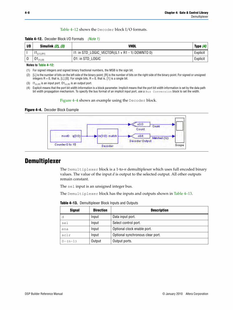
4–8 Chapter 4: Gate & Control LibraryDemultiplexer
Table 4–12 shows the Decoder block I/O formats.
Figure 4–4 shows an example using the Decoder block.
DemultiplexerThe Demultiplexer block is a 1-to-n demultiplexer which uses full encoded binary values. The value of the input d is output to the selected output. All other outputs remain constant.
The sel input is an unsigned integer bus.
The Demultiplexer block has the inputs and outputs shown in Table 4–13.
Table 4–12. Decoder Block I/O Formats (Note 1)
I/O Simulink (2), (3) VHDL Type (4)
I I1[L1].[R1] I1: in STD_LOGIC_VECTOR({L1 + R1 - 1} DOWNTO 0) Explicit
O O1[1].[0] O1: in STD_LOGIC Explicit
Notes to Table 4–12:
(1) For signed integers and signed binary fractional numbers, the MSB is the sign bit.(2) [L] is the number of bits on the left side of the binary point; [R] is the number of bits on the right side of the binary point. For signed or unsigned
integers R = 0, that is, [L].[0]. For single bits, R = 0, that is, [1] is a single bit.(3) I1[L].[R] is an input port. O1[L].[R] is an output port.(4) Explicit means that the port bit width information is a block parameter. Implicit means that the port bit width information is set by the data path
bit width propagation mechanism. To specify the bus format of an implicit input port, use a Bus Conversion block to set the width.
Figure 4–4. Decoder Block Example
Table 4–13. Demultiplexer Block Inputs and Outputs
Signal Direction Description
d Input Data input port.
sel Input Select control port.
ena Input Optional clock enable port.
sclr Input Optional synchronous clear port.
0–(n-1) Output Output ports.
DSP Builder Reference Manual © January 2010 Altera Corporation

Chapter 4: Gate & Control Library 4–9Demultiplexer
Table 4–14 describes the parameters for the Demultiplexer block.
Table 4–15 shows the Demultiplexer block I/O formats.
Figure 4–5 shows an example using the Demultiplexer block.
Table 4–14. Demultiplexer Block Parameters
Name Value Description
Number of Output Data Lines An integer greater than 1 (Parameterizable)
Specify how many outputs you want the demultiplexer to have.
Use Enable Port On or Off Turn on to use the clock enable input (ena).
Use Synchronous Clear Port On or Off Turn on to use the synchronous clear input (sclr).
Table 4–15. Demultiplexer Block I/O Formats (Note 2)
I/O Simulink (3), (4) VHDL Type (5)
I I1[L].[R]
I2[L].[R]
I3[1]
I4[1]
I1: in STD_LOGIC_VECTOR({L + R1 - 1} DOWNTO 0)
I2: in STD_LOGIC_VECTOR({L - 1} DOWNTO 0)
I3: in STD_LOGIC
I4: in STD_LOGIC
Implicit
Implicit
O O1[L].[R]
...
On[L].[R] (1)
O1: out STD_LOGIC_VECTOR({L + R - 1} DOWNTO 0)
...
On: out STD_LOGIC_VECTOR({L + R - 1} DOWNTO 0)
Implicit
Implicit
Notes to Table 4–15:
(1) Where I is the number of outputs to the demultiplexer.(2) For signed integers and signed binary fractional numbers, the MSB is the sign bit.(3) [L] is the number of bits on the left side of the binary point; [R] is the number of bits on the right side of the binary point. For signed or unsigned
integers R = 0, that is, [L].[0]. For single bits, R = 0, that is, [1] is a single bit.(4) I1[L].[R] is an input port. O1[L].[R] is an output port.(5) Explicit means that the port bit width information is a block parameter. Implicit means that the port bit width information is set by the data path
bit width propagation mechanism. To specify the bus format of an implicit input port, use a Bus Conversion block to set the width.
Figure 4–5. Demultiplexer Block Example
© January 2010 Altera Corporation DSP Builder Reference Manual

4–10 Chapter 4: Gate & Control LibraryFlipflop
FlipflopThe Flipflop block can be set as a D-type flipflop with enable (DFFE) or T-type flipflop with enable (TFFE).
If the number of bits is set to more than 1, the block behaves as single-bit flipflops for each bit. For example, for a TFFE flipflop with an n-bit signal, the signal is processed using n 1-bit TFFE flipflops.
The Flipflop block has the inputs and outputs shown in Table 4–16.
DFFE mode:
if (0 == aclrn) Q = 0;else if (0 == aprn) Q = 1;else if (1 == ena) Q = D
TFFE mode:
if (0 == aclrn) Q = 0;else if (0 == aprn) Q = 1; else if (1 == ena) and (1 == T) Q = toggle
1 Note that (aclrn == 0) and (aprn == 0) are not supported.
The aclrn port is an active-low asynchronous clear port. When active this sets the output and internal state to 0 for the remainder/duration of the clock cycle.
The aprn port is an active-low asynchronous preset port. When active this sets the output and internal state to 1 for the remainder/duration of the clock cycle.
Table 4–17 shows the Flipflop block parameters.
Table 4–16. Flipflop Block Inputs and Outputs
Signal Direction Description
input Input Data or togggle port.
ena Input Enable port.
aprn Input Asynchronous reset port.
aclrn Input Asynchronous clear port.
Q Output Output port.
Table 4–17. Flipflop Block Parameters
Name Value Description
Mode DFFE or TFFE Choose which type of flip flop to implement.
Bus Type Signed Integer, Signed Fractional, Unsigned Integer, Single Bit
Choose the bus number format that you want to use.
[number of bits].[] >= 0 (Parameterizable)
Specify the number of bits to the left of the binary point.
[].[number of bits] >= 0 (Parameterizable)
Specify the number of bits to the right of the binary point for the gain. This option is zero (0) unless Signed Fractional is selected.
DSP Builder Reference Manual © January 2010 Altera Corporation

Chapter 4: Gate & Control Library 4–11If Statement
Table 4–18 shows the Flipflop block I/O formats.
Figure 4–6 shows an example using the Flipflop block.
If StatementThe If Statement block outputs a 0 or 1 result based on the IF condition expression.
The If Statement block has the inputs and outputs shown in Table 4–19.
Table 4–18. Flipflop Block I/O Formats (Note 1)
I/O Simulink (2), (3) VHDL Type (4)
I I1[L1].[0]
I2[1].[0]
I3[1].[0]
I4[1].[0]
I1: in STD_LOGIC_VECTOR({L1 - 1} DOWNTO 0)
I2: in STD_LOGIC
I3: in STD_LOGIC
I4: in STD_LOGIC
Explicit
O O1[L1].[0] O1: in STD_LOGIC_VECTOR({L1 - 1} DOWNTO 0) Explicit
Notes to Table 4–18:
(1) For signed integers and signed binary fractional numbers, the MSB is the sign bit.(2) [L] is the number of bits on the left side of the binary point; [R] is the number of bits on the right side of the binary point. For signed or unsigned
integers R = 0, that is, [L].[0]. For single bits, R = 0, that is, [1] is a single bit.(3) I1[L].[R] is an input port. O1[L].[R] is an output port.(4) Explicit means that the port bit width information is a block parameter. Implicit means that the port bit width information is set by the data path
bit width propagation mechanism. To specify the bus format of an implicit input port, use a Bus Conversion block to set the width.
Figure 4–6. Flipflop Block Example
Table 4–19. If Statement Block Inputs and Outputs
Signal Direction Description
a–j Input Input ports.
n Input Optional ELSE IF input port.
true Output Output port (High when true).
false Output Optional ELSE output port (High when false).
© January 2010 Altera Corporation DSP Builder Reference Manual

4–12 Chapter 4: Gate & Control LibraryIf Statement
You can build an IF condition expression using the signal values 0 or 1 and any of the permitted operators given in Table 4–20.
When writing expressions in an If Statement block, ensure that the operators are always operating on the same types. That is, bus signals are compared with and operate with bus signals; and booleans (the 'true' or 'false' result of such operations) are only compared with and operate with booleans. In other words, the types must be the same on either side of an operator.
In an If statement expression, 0 and 1 are treated as signals rather than as booleans. Failure to ensure this, results in an error at HDL generation of the form:
Can't determine definition of operator "<mixed operator>" -- found 0 possible definitions
If you get an error of this form, you should carefully check the expressions specified in the If Statement blocks.
The following are examples of bad syntax that gives errors:
■ (a>b)&c, where a,b and c are all input values to the If Statement.
Here (a>b) returns a boolean ('true' or 'false') and is ANDed with signal c. This operation is ill defined and results in the error:
Can't determine definition of operator ""&"" -- found 0 possible definitions
■ ((a>b)~0)
Again (a>b) returns a boolean ('true' or 'false'). 0 is treated as a signal not a boolean, so the hardware generation fails with an error:
Can't determine definition of operator ""/="" -- found 0 possible definitions"
where /= is the hardware translation of the 'not equal to' operator. Here the ~0 is incorrectly used to mean 'not false', and is unnecessary. The correct syntax for this expression is just (a>b).
Table 4–20. Supported If Statement Block Operators
Operator Operation
& AND
| OR
$ XOR
= Equal To
~ Not Equal To
> Greater Than
< Less Than
() Parentheses
DSP Builder Reference Manual © January 2010 Altera Corporation

Chapter 4: Gate & Control Library 4–13If Statement
Table 4–21 shows the If Statement block parameters.
Table 4–22 shows the If Statement block I/O formats.
Table 4–21. If Statement Block Parameters
Name Value Description
Number of Inputs 2–10 Choose the number of inputs to the If Statement.
IF Expression User Defined Specify the if condition using any of the following operators: &, |, $, =, ~, >, <, or (), the variables a, b, c, d, e, f, g, h, i, or j, and the single digit numerals 0, 1.
Data Bus Type Signed Integer, Signed Fractional, Unsigned Integer Single Bit, Inferred
Choose the bus number format that you want to use. The selected type must be capable of expressing 0 and 1 exactly.
[number of bits].[] >= 0 (Parameterizable)
Specify the number of bits to the left of the binary point.
[].[number of bits] >= 0 (Parameterizable)
Specify the number of bits to the right of the binary point for the gain. This option is zero (0) unless Signed Fractional is selected.
Use ELSE Output Port On or Off This option turns on the false output, which implements an ELSE condition and goes high if the condition evaluated by the If Statement block is false.
Use ELSE IF Input Port
On or Off This option turns on the else input, which implements an ELSE IF input, when you want to cascade multiple IF Statement blocks together or as an enable for the block.
Table 4–22. If Statement Block I/O Formats (Note 1)
I/O Simulink (2), (3) VHDL Type (4)
I I1[L1].[R1]
….
Ii[LI].[RI]
…
In[LN].[RN]
I1: in STD_LOGIC_VECTOR({L1 + R1 - 1} DOWNTO 0)
…
Ii: in STD_LOGIC_VECTOR({LI + RI - 1} DOWNTO 0)
….
In: in STD_LOGIC_VECTOR({LN + RN - 1} DOWNTO 0)
Implicit
O O1[1]
O2[1]
O1: out STD_LOGIC
O2: out STD_LOGIC
Explicit
Notes to Table 4–22:
(1) For signed integers and signed binary fractional numbers, the MSB is the sign bit.(2) [L] is the number of bits on the left side of the binary point; [R] is the number of bits on the right side of the binary point. For signed or unsigned
integers R = 0, that is, [L].[0]. For single bits, R = 0, that is, [1] is a single bit.(3) I1[L].[R] is an input port. O1[L].[R] is an output port.(4) Explicit means that the port bit width information is a block parameter. Implicit means that the port bit width information is set by the data path
bit width propagation mechanism. To specify the bus format of an implicit input port, use a Bus Conversion block to set the width.
© January 2010 Altera Corporation DSP Builder Reference Manual

4–14 Chapter 4: Gate & Control LibraryLFSR Sequence
Figure 4–7 shows an example of using the If Statement block which implements the conditional statement:
Quantizer:if (Input<-4) Output = -100else if ((Input>=-4) & (Input<10)) Output = 0else Output = 100
LFSR SequenceThe LFSR Sequence block implements a linear feedback shift register which shifts one bit across L registers. The register output bits are shifted from least significant bit (LSB) to most significant bit (MSB) with the output sout connected to the MSB of the shift register. The register output bits can optionally be XORed or XNORed together.
For example, when choosing an LFSR sequence of length eight, the default polynomial is x8 + x4 + x3 + x2 + 1 with the circuitry shown in Figure 4–8.
In this default structure:
■ The polynomial is a primitive or maximal-length polynomial
■ All registers are initialized to one
■ The feedback gate type is XOR
■ The feedback structure is an external n-input gate or many to one
You can modify the implemented LFSR sequence by changing the parameter values.
Figure 4–7. If Statement Block Example
Figure 4–8. Default LFSR Sequence Block with Length 8 Circuitry
DSP Builder Reference Manual © January 2010 Altera Corporation

Chapter 4: Gate & Control Library 4–15LFSR Sequence
For example, after changing the feedback structure to an internal two-inputs gate, DSP Builder implements the circuitry shown in Figure 4–9.
This circuitry changes the sequence from:
1 1 1 1 1 1 1 1 0 0 1 0 0 0 0 1 0 1 0 0 1
to:
1 1 1 1 0 1 0 0 1 1 0 0 1 1 0 1 0 1 0 0 0
The LFSR Sequence block has the inputs and outputs shown in Table 4–23.
Table 4–24 shows the LFSR Sequence block parameters.
Figure 4–9. Internal 2-Input Gate Circuitry
Table 4–23. LFSR Sequence Block Inputs and Outputs
Signal Direction Description
ena Input Optional clock enable port.
rst Input Optional reset port.
sout Output Serial output port for MSB of the LFSR.
pout Output Optional parallel output port for LFSR unsigned value.
Table 4–24. LFSR Sequence Block Parameters (Part 1 of 2)
Name Value Description
LFSR Length User Defined (Parameterizable)
Specify the LFSR length as an integer.
Feedback Structure External n-inputs gate, Internal two-inputs gate
Choose whether you want an external n-inputs gate (many-to-one) or internal two-inputs gate (one-to-many) structure.
Feedback Gate Type XOR or XNOR Choose the type of feedback gate to implement.
Initial Register Value (Hex)
Any Hexadecimal Number (Parameterizable)
Specify the initial values in the register. If this value is larger than can be represented in the shift register (set by LFSR Length) the unrepresentable bits are truncated.
Primitive Polynomial Tap Sequence
User-Defined Array of Polynomial Coefficients (Parameterizable)
Specify where the taps occur in the shift register, 1 denotes the LSB and the LFSR length denotes the MSB. There must be a minimum of 2 taps. The numbers should be enclosed in square brackets. For example, [0 3 10].
Specify Clock On or Off Turn on to explicitly specify the clock name.
Clock User defined (Parameterizable)
Specify the name of the clock signal.
Use Parallel Output On or Off Turn on to use the parallel output (pout).
© January 2010 Altera Corporation DSP Builder Reference Manual

4–16 Chapter 4: Gate & Control LibraryLogical Bit Operator
Table 4–25 shows the LFSR Sequence block I/O formats.
Figure 4–10 shows an example using the LFSR Sequence block.
Logical Bit OperatorThe Logical Bit Operator block performs logical operations on single-bit inputs. You can specify a variable number of inputs. If the integer is positive, it is interpreted as a boolean 1, otherwise it is interpreted as 0. The number of inputs is variable.
Table 4–26 shows the Logical Bit Operator block parameters.
Use Enable Port On or Off Turn on to use the clock enable input (ena).
Use Synchronous Clear Port
On or Off Turn on to use the synchronous clear input (sclr).
Table 4–24. LFSR Sequence Block Parameters (Part 2 of 2)
Name Value Description
Table 4–25. LFSR Sequence Block I/O Formats (Note 1)
I/O Simulink (2), (3) VHDL Type
I I1[1].[0]
I2[1].[0]
I1: in STD_LOGIC
I2: in STD_LOGIC
—
—
O O1[1].[0]
O2[L].[0]
O1: out STD_LOGIC
O2: out STD_LOGIC_VECTOR(L-1 DOWNTO 0)
—
—
Notes to Table 4–25:
(1) For signed integers and signed binary fractional numbers, the MSB is the sign bit.(2) [L] is the number of bits on the left side of the binary point; [R] is the number of bits on the right side of the binary point. For signed or unsigned
integers R = 0, that is, [L].[0]. For single bits, R = 0, that is, [1] is a single bit.(3) I1[L].[R] is an input port. O1[L].[R] is an output port.
Figure 4–10. LFSR Sequence Block Example
Table 4–26. Logical Bit Operator Block Parameters
Name Value Description
Logical Operator AND, OR, XOR, NAND, NOR, NOT
Choose which operator you wish to use.
Number of Inputs 1–16 (Parameterizable)
Specify the number of inputs. This parameter defaults to 1 if the NOT logical operator is selected.
DSP Builder Reference Manual © January 2010 Altera Corporation

Chapter 4: Gate & Control Library 4–17Logical Bus Operator
Table 4–27 shows the Logical Bit Operator block I/O formats.
Figure 4–11 shows an example using the Logical Bit Operator block.
Logical Bus OperatorThe Logical Bus Operator block performs logical operations on a bus such as AND, OR, XOR, and invert. You can perform masking by entering a mask value in decimal notation, or a shift (rotate) operation by entering the number of bits. Note that, by default, a right shift operation preserves the input data sign (for signed inputs).
Table 4–27. Logical Bit Operator Block I/O Formats (Note 1)
I/O Simulink (2), (3) VHDL Type (4)
I I1[1]
…
Ii[1]
….
In[1]
I1: in STD_LOGIC
…
Ii: in STD_LOGIC
….
In: in STD_LOGIC
Explicit
O O1[1] O1: out STD_LOGIC Explicit
Notes to Table 4–27:
(1) For signed integers and signed binary fractional numbers, the MSB is the sign bit.(2) [L] is the number of bits on the left side of the binary point; [R] is the number of bits on the right side of the binary point. For signed or unsigned
integers R = 0, that is, [L].[0]. For single bits, R = 0, that is, [1] is a single bit.(3) I1[L].[R] is an input port. O1[L].[R] is an output port.(4) Explicit means that the port bit width information is a block parameter. Implicit means that the port bit width information is set by the data path
bit width propagation mechanism. To specify the bus format of an implicit input port, use a Bus Conversion block to set the width.
Figure 4–11. Logical Bit Operator Block Example
© January 2010 Altera Corporation DSP Builder Reference Manual

4–18 Chapter 4: Gate & Control LibraryLogical Bus Operator
The Logical Bus Operator block has the inputs and outputs shown in Table 4–28.
Table 4–29 shows the Logical Bus Operator block parameters.
Table 4–30 shows the Logical Bus Operator block I/O formats.
Table 4–28. Logical Bus Operator Block Inputs and Outputs
Signal Direction Description
d Input Input data.
q Output Output data.
Table 4–29. Logical Bus Operator Block Parameters
Name Value Description
Bus Type Signed Integer, Signed Fractional, Unsigned Integer
Choose the bus number format that you want to use.
[number of bits].[] >= 0 (Parameterizable)
Specify the number of bits to the left of the binary point, including the sign bit.
[].[number of bits] >= 0 (Parameterizable)
Specify the number of bits to the right of the binary point.
Logical Operation AND, OR, XOR, Invert, Shift Left, Shift Right, Rotate Left, Rotate Right
Choose the logical operation to perform.
Mask Value Integer (Parameterizable)
Specify the mask value for an AND, OR, or XOR operation as an unsigned integer representing the required mask which must have the same number of bits as the input.
Number of Bits to Shift User Defined (Parameterizable)
Specify how many bits you want to shift when a shift or rotate operation has been chosen.
Sign Extend On or Off Turn on to preserve the input data sign when right shifting signed data.
Table 4–30. Logical Bus Operator Block I/O Formats (Note 1)
I/O Simulink (2), (3) VHDL Type (4)
I I1[L1].[R1] I1: in STD_LOGIC_VECTOR({L1 + R1 - 1} DOWNTO 0) Explicit
O O1[L1].[R1] O1: out STD_LOGIC_VECTOR({L1 + R1 - 1} DOWNTO 0) Explicit
Notes to Table 4–30:
(1) For signed integers and signed binary fractional numbers, the MSB is the sign bit.(2) [L] is the number of bits on the left side of the binary point; [R] is the number of bits on the right side of the binary point. For signed or unsigned
integers R = 0, that is, [L].[0]. For single bits, R = 0, that is, [1] is a single bit.(3) I1[L].[R] is an input port. O1[L].[R] is an output port.(4) Explicit means that the port bit width information is a block parameter. Implicit means that the port bit width information is set by the data path
bit width propagation mechanism. To specify the bus format of an implicit input port, use a Bus Conversion block to set the width.
DSP Builder Reference Manual © January 2010 Altera Corporation

Chapter 4: Gate & Control Library 4–19Logical Reduce Operator
Figure 4–12 shows an example using the Logical Bus Operator block.
Logical Reduce OperatorThe Logical Reduce Operator block performs logical reduction operations on a bus such as AND, OR, XOR. The logical operation is applied bit-wise to the input bus to give a single bit result.
The Logical Reduce Operator block has the inputs and outputs shown in Table 4–31.
Table 4–32 shows the Logical Reduce Operator block parameters.
Figure 4–12. Logical Bus Operator Block Example
Table 4–31. Logical Reduce Operator Block Inputs and Outputs
Signal Direction Description
d Input Input data.
q Output Output result.
Table 4–32. Logical Reduce Operator Block Parameters (Part 1 of 2)
Name Value Description
Bus Type Inferred, Signed Integer, Signed Fractional, Unsigned Integer
Choose the bus number format that you want to use.
© January 2010 Altera Corporation DSP Builder Reference Manual

4–20 Chapter 4: Gate & Control LibraryLogical Reduce Operator
Table 4–33 shows the Logical Reduce Operator block I/O formats.
Figure 4–13 shows an example using the Logical Reduce Operator block.
[number of bits].[] >= 0 (Parameterizable)
Specify the number of bits to the left of the binary point, including the sign bit.
[].[number of bits] >= 0 (Parameterizable)
Specify the number of bits to the right of the binary point.
Logical Reduction Operation
AND, OR, XOR, NAND, NOR
Choose the logical operation to perform.
Table 4–32. Logical Reduce Operator Block Parameters (Part 2 of 2)
Name Value Description
Table 4–33. Logical Reduce Operator Block I/O Formats (Note 1)
I/O Simulink (2), (3) VHDL Type (4)
I I1[L1].[R1] I1: in STD_LOGIC_VECTOR({L1 + R1 - 1} DOWNTO 0) Explicit
O O1[1] O1: out STD_LOGIC Explicit
Notes to Table 4–30:
(1) For signed integers and signed binary fractional numbers, the MSB is the sign bit.(2) [L] is the number of bits on the left side of the binary point; [R] is the number of bits on the right side of the binary point. For signed or unsigned
integers R = 0, that is, [L].[0]. For single bits, R = 0, that is, [1] is a single bit.(3) I1[L].[R] is an input port. O1[L].[R] is an output port.(4) Explicit means that the port bit width information is a block parameter. Implicit means that the port bit width information is set by the data path
bit width propagation mechanism. To specify the bus format of an implicit input port, use a Bus Conversion block to set the width.
Figure 4–13. Logical Reduce Operator Block Example
DSP Builder Reference Manual © January 2010 Altera Corporation

Chapter 4: Gate & Control Library 4–21Multiplexer
MultiplexerThe Multiplexer block operates as either a n-to-1 one-hot or full binary bus multiplexer with one select control. The output width of the multiplexer is equal to the maximum width of the input data lines. The block works on any data type and sign extends the inputs if there is a bit width mismatch.
The Multiplexer block has the inputs and outputs shown in Table 4–34.
Table 4–35 shows the Multiplexer block parameters.
Table 4–36 shows the Multiplexer block I/O formats.
Table 4–34. Multiplexer Block Inputs and Outputs
Signal Direction Description
sel Input Select control port.
0–(n-1) Input Data input ports.
ena Input Optional enable port.
aclr Input Optional asynchronous clear port.
<unnamed> Output Output port.
Table 4–35. Multiplexer Block Parameters
Name Value Description
Number of Input Data Lines An integer greater than 1 (Parameterizable)
Specify how many inputs the multiplexer has.
Number of Pipeline Stages >= 0 (Parameterizable) Choose the number of pipeline stages.
One Hot Select Bus On or Off Turn on to use one-hot selection for the bus select signal instead of full binary.
Use Enable Port On or Off Turn on to use the clock enable input (ena). This option is available only when the number of pipeline stages is greater than 0.
Use Asynchronous Clear Port
On or Off Turn on to use the asynchronous clear input (aclr). This option is available only when the number of pipeline stages is greater than 0.
Table 4–36. Multiplexer Block I/O Formats (Part 1 of 2) (Note 1)
I/O Simulink (2), (3) VHDL Type (4)
I I1[LS].[0] (select input)
I2[L2].[R2]
….
Ii[Li].[Ri]
…
In[Ln].[Rn]
In+1[1]
In+2[1]
I1: in STD_LOGIC_VECTOR({L1 - 1} DOWNTO 0)
I2: in STD_LOGIC_VECTOR({L2 + R2 - 1} DOWNTO 0)
…
Ii: in STD_LOGIC_VECTOR({Li + Ri - 1} DOWNTO 0)
….
In: in STD_LOGIC_VECTOR({Ln + Rn - 1} DOWNTO 0)
In+1: STD_LOGIC
In+2: STD_LOGIC
Implicit
© January 2010 Altera Corporation DSP Builder Reference Manual

4–22 Chapter 4: Gate & Control LibraryPattern
Figure 4–14 shows an example using the Multiplexer block.
PatternThe Pattern block generates a repeating periodic bit sequence in time. You can enter the required pattern as a binary sequence.
For example, the pattern 01100 outputs the repeating pattern:
0110001100011000110001100011000110001100
You can change the output data rate for a registered block by feeding the clock enable input with the output of the Pattern block.
1 When used with a sequence of length 1 the Pattern block acts as a constant, holding its output to the specified value at all times. There is no artificial limit to the pattern length.
O O1[max(Li)].[max(Ri)]
with (0 < I < i + 1)
O1: out STD_LOGIC_VECTOR({max(Li)) + max(Ri) - 1} DOWNTO 0) Implicit
Notes to Table 4–36:
(1) For signed integers and signed binary fractional numbers, the MSB is the sign bit.(2) [L] is the number of bits on the left side of the binary point; [R] is the number of bits on the right side of the binary point. For signed or unsigned
integers R = 0, that is, [L].[0]. For single bits, R = 0, that is, [1] is a single bit.(3) I1[L].[R] is an input port. O1[L].[R] is an output port.(4) Explicit means that the port bit width information is a block parameter. Implicit means that the port bit width information is set by the data path
bit width propagation mechanism. To specify the bus format of an implicit input port, use a Bus Conversion block to set the width.
Table 4–36. Multiplexer Block I/O Formats (Part 2 of 2) (Note 1)
I/O Simulink (2), (3) VHDL Type (4)
Figure 4–14. Multiplexer Block Example
DSP Builder Reference Manual © January 2010 Altera Corporation

Chapter 4: Gate & Control Library 4–23Pattern
The Pattern block has the inputs and outputs shown in Table 4–37.
Table 4–38 shows the Pattern block parameters.
Table 4–39 shows the Pattern block I/O formats.
Figure 4–15 shows an example using the Pattern block.
Table 4–37. Pattern Block Inputs and Outputs
Signal Direction Description
ena Input Optional clock enable port.
sclr Input Optional synchronous clear port.
<unnamed> Output Output data port.
Table 4–38. Pattern Block Parameters
Name Value Description
Binary Sequence User Defined Specify the sequence that you wish to use.
Specify Clock On or Off Turn on to explicitly specify the clock name.
Clock User defined (Parameterizable)
Specify the name of the required clock signal.
Use Enable Port On or Off Turn on to use the clock enable input (ena).
Use Synchronous Clear Port On or Off Turn on to use the synchronous clear input (sclr).
Table 4–39. Pattern Block I/O Formats (Note 1)
I/O Simulink (2), (3) VHDL Type (4)
I I1[1]
I2[1]
I1: in STD_LOGIC
I2: in STD_LOGIC
Explicit - optional
Explicit - optional
O O1[1] O1: out STD_LOGIC Explicit
Notes to Table 4–39:
(1) For signed integers and signed binary fractional numbers, the MSB is the sign bit.(2) [L] is the number of bits on the left side of the binary point; [R] is the number of bits on the right side of the binary point. For signed or unsigned
integers R = 0, that is, [L].[0]. For single bits, R = 0, that is, [1] is a single bit.(3) I1[L].[R] is an input port. O1[L].[R] is an output port.(4) Explicit means that the port bit width information is a block parameter. Implicit means that the port bit width information is set by the data path
bit width propagation mechanism. To specify the bus format of an implicit input port, use a Bus Conversion block to set the width.
Figure 4–15. Pattern Block Example
© January 2010 Altera Corporation DSP Builder Reference Manual

4–24 Chapter 4: Gate & Control LibrarySingle Pulse
Single PulseThe Single Pulse block generates a single pulse output signal. The output signal is a single bit that takes only the values 1 or 0. The signal generation type could be an Impulse, a Step Up (0 to 1), or a Step Down (1 to 0).
The output of a Impulse starts at 0 changing to 1 after a specified delay and changing to 0 again after a specified length. The output of a Step Up starts at 0 changing to 1 after a specified delay. The output of a Step Down starts at 1 changing to 0 after a specified delay.
The Single Pulse block has the inputs and outputs shown in Table 4–40.
Table 4–41 shows the Single Pulse block parameters.
Table 4–42 shows the Single Pulse block I/O formats.
Table 4–40. Single Pulse Block Inputs and Outputs
Signal Direction Description
ena Input Optional clock enable port.
sclr Input Optional synchronous clear port.
<unnamed> output Output port.
Table 4–41. Single Pulse Block Parameters
Name Value Description
Signal Generation Type Step Up, Step Down, Impulse
Choose the type of single pulse.
Impulse Length Integer (Parameterizable)
Specify the number of clock cycles for which the output signal is transitional from 0 to 1 for an Impulse type output.
Delay Integer (Parameterizable)
Specify the number of clock cycles which occur before the pulse transition.
Specify Clock On or Off Turn on to explicitly specify the clock name.
Clock User defined (Parameterizable)
Specify the name of the required clock signal.
Use Enable Port On or Off Turn on to use the clock enable input (ena).
Use Synchronous Clear Port On or Off Turn on to use the synchronous clear input (sclr).
Table 4–42. Single Pulse Block I/O Formats
I/O Simulink (1) VHDL Type
I I1[1]
I2[1]
I1: in STD_LOGIC
I2: in STD_LOGIC
Optional trigger
Optional reset
O O1[1] O1: out STD_LOGIC —
Notes to Table 4–42:
(1) I1[1] is an input port. O1[1] is an output port.
DSP Builder Reference Manual © January 2010 Altera Corporation

Chapter 4: Gate & Control Library 4–25Single Pulse
Figure 4–16. shows an example of a Single Pulse block.
Figure 4–16. Single Pulse Output Signal Types
© January 2010 Altera Corporation DSP Builder Reference Manual

4–26 Chapter 4: Gate & Control LibrarySingle Pulse
DSP Builder Reference Manual © January 2010 Altera Corporation

© January 2010 Altera Corporation
5. Interfaces Library
You can use the blocks in the Interfaces library to build custom logic blocks that supports the Avalon® Memory-Mapped (Avalon-MM) and Avalon Streaming (Avalon-ST) interfaces.
The Interfaces library contains the following blocks:
■ Avalon-MM Master
■ Avalon-MM Slave
■ Avalon-MM Read FIFO
■ Avalon-MM Write FIFO
■ Avalon-ST Packet Format Converter
■ Avalon-ST Sink
■ Avalon-ST Source
Avalon Memory-Mapped BlocksThe Avalon Memory-Mapped blocks automate the process of specifying master and slave ports that are compatible with the Avalon-MM bus.
After you build a model of your DSP Builder peripheral, you can add blocks to control the peripheral’s inputs and outputs. These include:
■ Configurable master and slave blocks which contain the ports required to connect peripherals that use the Avalon-MM bus.
■ Wrapped versions of the Avalon-MM slave which implement an Avalon-MM read FIFO and Avalon-MM write FIFO.
f For more information about the Avalon-MM interface, refer to the Avalon Interface Specifications.
After you synthesize your model and compile it in the Quartus II software, you can add it to your Nios II system using SOPC Builder.
Your design automatically appears under the DSP Builder category in the SOPC Builder component browser peripherals listing provided that the MDL file is in the same directory as the SOPC file.
A file mydesign.mdl creates a component mydesign_interface in SOPC Builder.
1 For the peripheral to appear in SOPC Builder, the working directory for your SOPC Builder project must be the same as your DSP Builder working directory.
f For information about using SOPC Builder to create Nios II designs, refer to the Nios II Hardware Development Tutorial.
DSP Builder Reference Manual

5–2 Chapter 5: Interfaces Library
Figure 5–1 shows SOPC Builder with an on-chip RAM memory, Nios II processor, and a DSP Builder created peripheral named topavalon.
Figure 5–2 shows the design flow using DSP Builder and SOPC Builder.
Figure 5–1. SOPC Builder with DSP Builder Peripheral
Figure 5–2. DSP Builder & SOPC Builder Design Flow
DSP Builder Reference Manual © January 2010 Altera Corporation

Chapter 5: Interfaces Library 5–3Avalon-MM Master
Figure 5–3 shows an example model using Avalon-MM blocks.
Avalon-MM MasterThe Avalon-MM Master block defines a collection of ports for connection to an SOPC Builder system when your design functions as an Avalon-MM master interface.
Table 5–1 lists the signals supported by the Avalon-MM Master block.
Figure 5–3. Avalon-MM Blocks Example
Table 5–1. Signals Supported by the Avalon-MM Master Block (Part 1 of 2)
Signal Direction Description
waitrequest Input This signal forces the master port to wait until you are ready to proceed with the transfer.
address Output The address signal represents a byte address but is asserted on word boundaries only.
read Output Available when Read or Read/Write address type is chosen. Read request signal. Not required if there are no read transfers. If used, readdata must also be used.
readdata Input Available when Read or Read/Write address type is chosen. Data lines for read transfers. Not required if there are no read transfers. If used, read must also be used.
write Output Available when Write or Read/Write address type is chosen. Write request signal. Not required if there are no write transfers. If used, writedata must also be used.
writedata Output Available when Write or Read/Write address type is chosen. Data lines for write transfers. Not required if there are no write transfers. If used, write must also be used.
byteenable Output Available when Write or Read/Write address type is chosen and the bit width is greater than 8. Enables specific byte lane(s) during write transfers to memories of width greater than 8 bits. All byteenable lines must be enabled during read transfers.
endofpacket Input Available when Allow Flow Control is on. Indicates an end-of-packet condition.
© January 2010 Altera Corporation DSP Builder Reference Manual

5–4 Chapter 5: Interfaces LibraryAvalon-MM Master
1 The direction in Table 5–1 refers to the direction in respect of the DSP Builder block interface.
Figure 5–2 shows the Avalon-MM Master block parameters.
readdatavalid Input Available when Allow Pipeline Transfers is on. Used for pipelined read transfers with latency. Indicates that valid data is present on the readdata lines.
flush Output Available when Allow Pipeline Transfers and Use Flush Signal are on. Can be asserted to clear any pending transfers in the pipeline.
burstcount Output Available when Allow Burst Transfers is on. Indicates the number of transfers in a burst.
irq Input Available when Receive IRQ is on. Indicates when one or more ports have requested an interrupt.
irqnumber Input Available when Receive IRQ is on and IRQ mode is set to Prioritized. Indicates the interrupt priority. Lower value means higher priority.
Table 5–1. Signals Supported by the Avalon-MM Master Block (Part 2 of 2)
Signal Direction Description
Table 5–2. Avalon-MM Master Block Parameters (Part 1 of 2)
Name Value Description
Specify Clock On or Off Turn on to explicitly specify the clock name.
Clock User defined Specify the clock signal name.
Address Width 1–32 Specify the number of address bits.
Address Type Read, Write, Read/Write
Choose the address type for the bus.
Data Type Signed Integer, Signed Fractional, Unsigned Integer
Choose the number format of the bus.
[number of bits].[] >= 0 (Parameterizable)
Specify the number of bits to the left of the binary point, including the sign bit. Read and write buses must have the same number of bits.
[].[number of bits] >= 0 (Parameterizable)
Specify the number of bits to the right of the binary point. This parameter applies only to signed fractional buses.
Allow Byte Enable On or Off Turn on to use the Byte Enable signal. This option is available when the address type is set to Write or Read/Write and the bit width is greater than 8.
Allow Flow Control On or Off Turn on to enable flow control. Flow control allows a slave port to regulate incoming transfers from a master port, so that a transfer only begins when the slave port indicates that it has valid data or is ready to receive data.
Allow Pipeline Transfers
On or Off Turn on to allow pipeline transfers. Pipeline transfers increase the bandwidth for synchronous slave peripherals that require several cycles to return data for the first access, but can return data every cycle thereafter. This option is available when the address type is Read or Read/Write.
Use Flush Signal On or Off Turn on to clear any pending transfers in the pipeline. This option is available when Allow Pipeline Transfers is on.
Allow Burst Transfers On or Off Turn on to allow burst transfers. A burst executes multiple transfers as a unit, and maximize the throughput for slave ports that will achieve the greatest efficiency when handling multiple units of data from one master port at a time.
Maximum Burst Size 2–32 Specify the maximum width of a burst transfer. This option is available when Allow Burst Transfers is on.
DSP Builder Reference Manual © January 2010 Altera Corporation
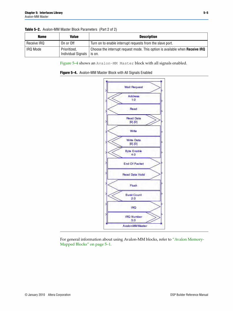
Chapter 5: Interfaces Library 5–5Avalon-MM Master
Figure 5–4 shows an Avalon-MM Master block with all signals enabled.
For general information about using Avalon-MM blocks, refer to “Avalon Memory-Mapped Blocks” on page 5–1.
Receive IRQ On or Off Turn on to enable interrupt requests from the slave port.
IRQ Mode Prioritized, Individual Signals
Choose the interrupt request mode. This option is available when Receive IRQ is on.
Table 5–2. Avalon-MM Master Block Parameters (Part 2 of 2)
Name Value Description
Figure 5–4. Avalon-MM Master Block with All Signals Enabled
© January 2010 Altera Corporation DSP Builder Reference Manual

5–6 Chapter 5: Interfaces LibraryAvalon-MM Slave
Avalon-MM SlaveThe Avalon-MM Slave block defines a collection of ports for connection to an SOPC Builder system when your design functions as an Avalon-MM slave interface.
Table 5–3 lists the signals supported by the Avalon-MM Slave block.
1 The direction in Table 5–3 refers to the direction in respect of the DSP Builder block interface.
Table 5–3. Signals Supported by the Avalon-MM Slave Block
Signal Direction Description
address Output Address lines to the slave port. Specifies a word offset into the slave address space.
read Output Available when Read or Read/Write address type is chosen. Read-request signal. Not required if there are no read transfers. If used, readdata must also be used.
readdata Input Available when Read or Read/Write address type is chosen. Data lines for read transfers. Not required if there are no read transfers. If used, read must also be used.
write Output Available when Write or Read/Write address type is chosen. Write-request signal. Not required if there are no write transfers. If used, writedata must also be used.
writedata Output Available when Write or Read/Write address type is chosen. Data lines for write transfers. Not required if there are no write transfers. If used, write must also be used.
byteenable Output Available when Allow Byte Enable is on and the bit width is greater than 8. Byte-enable signals to enable specific byte lane(s) during write transfers to memories of width greater than 8 bits. If used, writedata must also be used.
readyfordata Input Available when Write or Read/Write access is chosen and Allow Flow Control is on. Indicates that the peripheral is ready for a write transfer.
dataavailable Input Available when Read or Read/Write access is chosen and Allow Flow Control is on. Indicates that the peripheral is ready for a read transfer.
endofpacket Input Available when Allow Flow Control is on. Indicates an end-of-packet condition.
readdatavalid Input Available when Allow Pipeline Transfers is on and variable read latency is chosen. Marks the rising clock edge when readdata is asserted.
waitrequest Input Available when variable wait-state format is chosen. Used to stall the interface when the slave port is not able to respond immediately.
beginbursttransfer Output Available when Allow Burst Transfers is on. Asserted for the first cycle of a burst to indicate when a burst transfer is starting.
burstcount Output Available when Allow Burst Transfers is on. Indicates the number of transfers in a burst. If used, waitrequest must also be used.
irq Input Available when Output IRQ is on. Interrupt request. Asserted when a port needs to be serviced.
begintransfer Output Available when Receive Begin Transfer is on. Asserted during the first cycle of every transfer.
chipselect Output Available when Use Chip Select is on. The slave port ignores all other Avalon-MM signal inputs unless chipselect is asserted.
DSP Builder Reference Manual © January 2010 Altera Corporation

Chapter 5: Interfaces Library 5–7Avalon-MM Slave
Table 5–4 shows the Avalon-MM Slave block parameters.
Table 5–4. Avalon-MM Slave Block Parameters
Name Value Description
Specify Clock On or Off Turn on to explicitly specify the clock name.
Clock User defined Specify the clock signal name.
Address Width 1–32 Specify the number of address bits.
Address Alignment Native, Dynamic Choose whether to use native address alignment or dynamic bus sizing.
Address Type Read, Write, Read/Write
Choose the address type for the bus.
Data Type Signed Integer, Signed Fractional, Unsigned Integer
Choose the number format of the bus.
[number of bits].[] >= 0 (Parameterizable)
Specify the number of bits to the left of the binary point, including the sign bit. Read and write buses must have the same number of bits.
[].[number of bits] >= 0 (Parameterizable)
Specify the number of bits to the right of the binary point. This parameter applies only to signed fractional buses.
Allow Byte Enable On or Off Turn on to use the Byte Enable signal. This option is available only when the address type is set to Write or Read/Write.
Allow Flow Control On or Off Turn on to enable flow control. Flow control allows a slave port to regulate incoming transfers from a master port, so that a transfer only begins when the slave port indicates that it has valid data or is ready to receive data.
Allow Pipeline Transfers
On or Off Turn on to allow pipeline transfers. Pipeline transfers increase the bandwidth for synchronous slave peripherals that require several cycles to return data for the first access, but can return data every cycle thereafter. This option is available only when the address type is set to Read or Read/Write.
Wait-State Format Fixed, Variable Choose the required wait-state format.
Read Wait-State Cycles 0–255 Specify the number of read wait-state cycles. This option is available only when the wait-state format is set to Fixed.
Write Wait-State Cycles 0–255 Specify the number of write wait state cycles. This option is available only when the wait-state format is set to Fixed.
Read Latency Format Fixed, Variable Choose the required read latency format. This option is available only when Allow Pipeline Transfers is on.
Read Latency Cycles 0–8 Specify the pipeline read latency. Latency determines the length of the data phase, independently of the address phase. For example, a pipelined slave port (with no wait-states) can sustain one transfer per cycle, even though it may require several cycles of latency to return the first unit of data. This option is available only when Allow Pipeline Transfers is on and Fixed read latency format is set.
Allow Burst Transfers On or Off Turn on to allow burst transfers. A burst executes multiple transfers as a unit, and maximize the throughput for slave ports that will achieve the greatest efficiency when handling multiple units of data from one master port at a time.
Maximum Burst Size 4–232 Specify the maximum width of a burst transfer. This option is available only when Allow Burst Transfer is on.
Output IRQ On or Off Turn on to enable interrupt requests from the slave port.
Receive BeginTransfer On or Off Turn on to receive begintransfer signals.
Use Chip Select On or Off Turn on to enable the chipselect signal.
© January 2010 Altera Corporation DSP Builder Reference Manual

5–8 Chapter 5: Interfaces LibraryAvalon-MM Slave
Figure 5–5 shows an Avalon-MM Slave block with all signals enabled.
For general information about using Avalon-MM blocks refer to “Avalon Memory-Mapped Blocks” on page 5–1.
Figure 5–5. Avalon-MM Slave Block with All Signals Enabled
DSP Builder Reference Manual © January 2010 Altera Corporation

Chapter 5: Interfaces Library 5–9Avalon-MM Read FIFO
Avalon-MM Read FIFOThe Avalon-MM Read FIFO block is essentially an Avalon-MM Slave block configured to implement a read FIFO. It is accessed by other Avalon-MM peripherals to obtain data when connected in SOPC Builder.
For information about the Avalon-MM Slave block, refer to “Avalon-MM Slave” on page 5–6.
Table 5–5 lists the signals supported by the Avalon-MM Read FIFO block.
Table 5–6 shows the Avalon-MM Read FIFO block parameters.
Table 5–5. Signals Supported by the Avalon-MM Read FIFO Block
Signal Direction Description
Stall Input This port must be connected to Simulink blocks. It simulates stall conditions of the Avalon-MM bus and hence back pressure to the SOPC component. For any simulation cycle where the Stall signal is asserted, no Avalon-MM reads take place and the internal FIFO fills. When full, the Ready output is de-asserted so that no data is lost.
Data Input This port should be connected to DSP Builder blocks and should be connected to outgoing data from the user design.
DataValid Input This port should be connected to DSP Builder blocks and should be asserted whenever the signal on the Data port corresponds to real data.
TestDataOut Output This port should be connected to Simulink blocks and corresponds to the data received over the Avalon-MM bus.
TestDataValid Output This port should be connected to Simulink blocks and is asserted whenever TestDataOut corresponds to real data.
Ready Output When asserted, indicates that the block is ready to receive data.
Table 5–6. Avalon-MM Read FIFO Block Parameters
Name Value Description
Data Type Signed Integer, Signed Fractional, Unsigned Integer
Choose the number format of the bus.
[number of bits].[] >= 0 (Parameterizable)
Specify the number of bits to the left of the binary point, including the sign bit. This parameter does not apply to single-bit buses.
[].[number of bits] >= 0 (Parameterizable)
Specify the number of bits to the right of the binary point. This parameter applies only to signed fractional buses.
FIFO Depth > 2 Specify the depth of the FIFO.
© January 2010 Altera Corporation DSP Builder Reference Manual

5–10 Chapter 5: Interfaces LibraryAvalon-MM Read FIFO
Figure 5–6 shows an Avalon-MM Read FIFO block.
Figure 5–7 shows the content of the Avalon-MM Read FIFO block.
Figure 5–6. Avalon-MM Read FIFO
Figure 5–7. Avalon-MM Read FIFO Content
DSP Builder Reference Manual © January 2010 Altera Corporation

Chapter 5: Interfaces Library 5–11Avalon-MM Write FIFO
Avalon-MM Write FIFOThe Avalon-MM Write FIFO block is essentially an Avalon-MM Slave block configured to implement a write FIFO.
For information about the Avalon-MM Slave block, refer to “Avalon-MM Slave” on page 5–6.
Table 5–7 lists the signals supported by the Avalon-MM Write FIFO block.
Table 5–8 shows the Avalon-MM Write FIFO block parameters.
Figure 5–8 shows an Avalon-MM Write FIFO block.
Table 5–7. Signals Supported by the Avalon-MM Write FIFO Block
Signal Direction Description
TestData Input This port must be connected to Simulink blocks. It provides simulation data to the Avalon-MM write FIFO. The data is passed to the DataOut port one cycle after the Ready input port is asserted.
Stall Input This port must be connected to Simulink blocks. It simulates stall conditions of the Avalon-MM bus and hence underflow to the SOPC component. For any simulation cycle where Stall is asserted, the test data is cached by the Avalon-MM write converter and released in order, one sample per clock, when stall is de-asserted.
Ready Input This port must be connected to DSP Builder blocks. It indicates that the downstream hardware is ready for data.
DataOut Output This port should be connected to DSP Builder blocks and corresponds to the oldest unsent data sample received on the TestData port.
DataValid Output This port should be connected to DSP Builder blocks and is asserted whenever DataOut corresponds to real data.
Table 5–8. Avalon-MM Write FIFO Block Parameters
Name Value Description
Data Type Signed Integer, Signed Fractional, Unsigned Integer
Choose the number format of the bus.
[number of bits].[] >= 0 (Parameterizable)
Specify the number of bits to the left of the binary point, including the sign bit. This parameter does not apply to single-bit buses.
[].[number of bits] >= 0 (Parameterizable)
Specify the number of bits to the right of the binary point. This parameter applies only to signed fractional buses.
FIFO Depth > 2 Specify the depth of the FIFO.
Figure 5–8. Avalon-MM Write FIFO
© January 2010 Altera Corporation DSP Builder Reference Manual

5–12 Chapter 5: Interfaces LibraryAvalon-ST Packet Format Converter
Figure 5–9 shows the content of the Avalon-MM Write FIFO block.
Avalon Streaming BlocksThe Avalon Streaming blocks automate the process of specifying ports that are compatible with an Avalon-ST interface. The blocks include an Avalon-ST Packet Format Converter, Avalon-ST Sink and Avalon-ST Source.
f For information about the Avalon-ST interface, refer to the Avalon Interface Specifications.
Avalon-ST Packet Format ConverterThe Avalon-ST Packet Format Converter (PFC) block transforms packets received from one block to a different packet format required by another block.
The PFC takes packet data from one or more input interfaces, and provides field reassignment in time and space to one or more output packet interfaces. You specify the input packet format and the desired output packet format, then the appropriate control logic is automatically generated.
The PFC operates on a single clock domain, and supports multicast data, where an input field is broadcast copied to multiple output fields. The ready latency of the PFC block is zero and it can only be connected to other Avalon-ST interfaces with a ready latency of zero.
1 Verilog HDL is generated for the PFC block and you must therefore have a license that supports Verilog HDL when simulating in ModelSim.
Figure 5–9. Avalon-MM Write FIFO Content
DSP Builder Reference Manual © January 2010 Altera Corporation

Chapter 5: Interfaces Library 5–13Avalon-ST Packet Format Converter
The basic operation of the PFC is shown in Figure 5–10.
The PFC performs data mapping on a packet by packet basis, so that there is exactly one input packet on each input interface for one output packet on each output interface. This means that the packet rate of the converter is limited by the interface with the longest packet.
When the PFC has multiple output interfaces, the packets on each output interface are aligned so that the startofpacket signal is presented on the same clock cycle.
If each interface supports fixed-length packets, a Multi-Packet Mapping option can be selected. The PFC can then map fields from multiple input packets to multiple output packets. The PFC does not support bursts or blocks on its output interfaces.
You can use the Split Data option to split the input or output data signals across additional ports named data0 through dataN.
Each input interface consists of the ready, valid, startofpacket, endofpacket, empty, and data signals. Each output interface has an additional error signal which is asserted to indicate a frame delineation error.
f For more information about these signal types, refer to the Avalon Interface Specifications.
1 The PFC block does not support Avalon-ST bursts or blocks on its output interfaces.
Table 5–9 lists the signals supported by the Avalon-ST Packet Format Converter block.
Figure 5–10. Basic Packet Format Converter
Table 5–9. Signals Supported by the Avalon-ST Packet Format Converter Block (Part 1 of 2)
Signal Direction Description
reset_n Input Active-low reset signal.
inX_dataN Input Data input bus for sink interface X.
inX_empty Input Indicates the number of empty symbols for sink interface X during cycles that mark the end of a packet.
© January 2010 Altera Corporation DSP Builder Reference Manual

5–14 Chapter 5: Interfaces LibraryAvalon-ST Packet Format Converter
Table 5–10 shows the Avalon-ST Packet Format Converter block parameters.
inX_endofpacket Input This signal marks the active cycle containing the end of the packet for sink interface X.
inX_startofpacket Input This signal marks the active cycle containing the start of the packet for sink interface X.
inX_valid Input Indicates that data can be accepted for sink interface X.
outY_ready Input Indicates that the sink driven by the source interface Y is ready to accept data.
aclr Input Optional asynchronous clear port.
inX_ready Output Indicates that sink interface X is ready to output data.
outY_dataN Output Data output bus for source interface Y.
outY_empty Output Indicates the number of empty symbols for source interface Y during cycles that mark the end of a packet.
outY_endofpacket Output This signal marks the active cycle containing the end of the packet for source interface Y.
outY_startofpacket Output This signal marks the active cycle containing the start of the packet for source interface Y.
outY_valid Output Indicates that valid data is available on source interface Y.
outYerror Output Indicates an error condition when asserted high.
Table 5–9. Signals Supported by the Avalon-ST Packet Format Converter Block (Part 2 of 2)
Signal Direction Description
Table 5–10. Avalon-ST Packet Format Converter Block Parameters
Name Value Description
Number of Sinks 1–16 Specifies the number of sink interfaces X.
Number of Sources 1–16 Specifies the number of source interfaces Y.
Split Data On or Off When on, the data signals on the sink and source interface are split into signals named data0 through dataN with widths corresponding to the specified symbol width.
Multi-Packet Mapping On or Off When off, one input packet is matched to one output packet and the input and output packets must have the name number of instances in each field. When on, the PFC maps the input packets to output packets such that all instances of every data field are accounted for.
Symbol Width >= 1 Specifies the number of bits per symbol used by all the PFC sink and source interfaces.
Use Asynchronous Clear Port
On or Off Turn on to use the asynchronous clear input (aclr).
Sink Format X string A quoted string or MATLAB variable which describes the packet format for sink interface X.
Sink X Symbols Per Beat 1–32 Specifies the number of symbols per beat for sink interface X.
Source Format Y string A quoted string or MATLAB variable which describes the packet format for source interface Y.
Source Y Symbols Per Beat 1–32 Specifies number of symbols per beat for source interface Y.
DSP Builder Reference Manual © January 2010 Altera Corporation

Chapter 5: Interfaces Library 5–15Avalon-ST Packet Format Converter
PFC Data FlowThe PFC spools data into a FIFO-like memory as it arrives, and spools it out in a different order as it leaves. The data can be provided at the output of each interface as soon as it has been written into the memory and all previous output data has been transferred. When the PFC has multiple output interfaces, the startofpacket signal for all the interfaces is asserted at the same time.
The PFC stops data input on input interfaces by deasserting the ready signal whenever there is a risk of overwriting data that has not yet been output. If a downstream block pauses output data by deasserting the ready signal to the PFC, data is accepted into the PFC until unsent data is at risk of being overwritten. At this point, the PFC deasserts the ready signals on its own input interface, causing the upstream block to stop sending data.
In a similar way, if the upstream block starves the PFC of data by deasserting the valid signals to the PFC, then the PFC output interface continues to send data until the memory is drained. It then stops sending data by deasserting the output valid signals.
For multiple interface PFC blocks, back pressuring an output interface or starving an input interface affects all other interfaces. When an output interface is back pressured, the input interfaces are back pressured as well, causing the other outputs to be starved of data. Likewise, if an input interface is starved of data, the output interfaces eventually stop, causing the other input interfaces to be back pressured.
Packet Format DescriptionFor each input and output interface, the basic format of the packet is described by the number of symbols per beat and the packet description.
The number of symbols per beat defines, for each interface, the number of symbols that are presented in parallel on every active cycle. The packet description is a string which describes the fields in the packet.
A basic packet description is a comma-separated list of field names, where a field name includes any of the characters a-z, A-Z, _, or 0-9 but must start with a letter. For example: Field1, Red, Green, Blue, and DestinationAddress. Field names are case sensitive. Whitespace is not permitted in a packet description.
If fields are repeated in a packet, parentheses are used to delineate the repeated group (of one or more fields), and a positive integer follows the group to indicate the number of repeats. This use of this parenthesis is described further in the following examples:
■ Dest,Source,(Data)128,(CRC)4 indicates a packet that has destination and source address symbols followed by 128 data symbols and 4 CRC symbols.
■ (Red,Green,Blue)100 refers to a frame with 100 repetitions of a symbol of Red, followed by a symbol of Green, followed by a symbol of Blue.
■ Repeats can be nested, so that (F1,(F2)3,F3)2,F4 is equivalent to (F1,F2,F2,F2,F3)2,F4 or F1,F2,F2,F2,F3,F1,F2,F2,F2,F3,F4.
© January 2010 Altera Corporation DSP Builder Reference Manual

5–16 Chapter 5: Interfaces LibraryAvalon-ST Packet Format Converter
A group can be repeated an unspecified number of times in a packet, by using a + instead of a positive integer, such as (Red,Green,Blue)+. However, such a group must compose the entire packet. Therefore, none of the following examples are valid: A,(B,C)+, (A,B)+,C, or((A)+)2.
Table 5–11 summarizes the packet description syntax for the PFC.
Table 5–12 shows some example packets. All these examples use the convention <packet description> / <symbols per beat>, so that R,G,B/2 refers to an interface where the packet description is R,G,B and the number of symbols per beat is 2.
Table 5–11. Packet Description Syntax
Packet Descriptor: Group | (Group)+
where + indicates that the preceding Group is repeated an unknown number of times
Group repeatedGroup | simpleGroup
repeatedGroup (Group)N
where N is a positive integer indicating the number of times the preceding group is repeated
simpleGroup FieldName[,Group]
Table 5–12. Packet Description Examples
Packet Description / Symbols Per Beat Example Packets
(R,G,B)4
(R,G,B)4/3
(Y,Cr,Y,Cb)/2
((A)2,B,C,(A)2,B,D)3/4
((((A)2,B)2,C)2,D)2
DSP Builder Reference Manual © January 2010 Altera Corporation

Chapter 5: Interfaces Library 5–17Avalon-ST Packet Format Converter
Figure 5–11 shows an example of the packet formats for a PFC with two input and two output interfaces.
Packet MappingPacket mapping is the process of determining where the data for each field in each output interface is coming from (as an {input interface, position} pair).
Packet mapping is achieved by comparing the field name strings. For example, the source of data for the Red field in a given output interface is the field on an input interface with the name Red. It is not valid for any field name to exist on multiple-input interfaces; no two input interfaces may have a Red field. It is valid, however, for multiple-output interfaces to have the same field; the Red data may be copied to two or more output interfaces.
A single input or output interface can have multiple instances of the same field. For example, Red,Green,Red,Blue represents a packet with two red symbols per packet. The PFC matches the nth instance of a field on an input interface to the nth instance of the same field on an output interface. If an output interface has Blue,Green,Red,Red, the data for the first Red field is taken from the first Red field in the input packet.
Each output interface may or may not use a given input field, but unless the Multi-Packet Mapping option is set (and if the input field is used) there must be the same number of instances of the field in each output as there is in the input. For example, Green and Red,Red,Green are both valid, but Red,Green is not.
Multi-Packet MappingWhen the Multi-Packet Mapping option is set, the PFC is not limited to mapping a single input packet on each port to a single output packet on each port. It can map multiple input packets to multiple output packets.
For example, (Red,Green,Blue)2 maps to (Red,Green,Blue)3 by using three input packets for every two output packets.
Figure 5–11. Example of a Packet Format Converter with Two Input and Two Output Interfaces
© January 2010 Altera Corporation DSP Builder Reference Manual

5–18 Chapter 5: Interfaces LibraryAvalon-ST Packet Format Converter
The ratio of input fields to output fields must be constant.
For example, Red,Red,Green,Blue will not map to (Red,Green,Blue)2 because each output packet requires one input packet for Red, but two input packets for Green and Blue.
Multiple interfaces are supported but the packet ratio must be constant across all {input interface, output interface} pairs.
For example, two input interfaces with the formats (Red,Green)2 and Blue would map to output interface (Red)6,Blue(3),Green(6) because three input packets are required for two output packets for all input/output pairs. The same inputs would not map to (Red)3,Blue(3),Green(3), because to make two output packets, three of the first input's packets and six of the second input's packets are required.
1 Packets of unknown length are not supported in DSP Builder.
Error HandlingThe PFC contains internal counters that keep track of the current position in the packet for each input and uses these counters to detect frame delineation errors. Every time a startofpacket or endofpacket signal is asserted on an input interface, the PFC uses its knowledge of the frame structure to ensure that the assertion is on a valid cycle. For PFC variants where the packet size is known, the PFC also checks that the startofpacket and endofpacket signals are asserted when they should be, and are not missed.
The PFC only has a single output error bit to report frame delineation errors. The output error bit is asserted on all outputs as soon as an error is detected, and it is held asserted for each output interface independently until an endofpacket has been asserted for that output interface.
After the endofpacket has been asserted, no more data is presented to that output interface. When all output interfaces are stopped, the PFC resets itself and resumes normal operation. The PFC stops independently on the endofpacket signal for each output, and components downstream of the PFC should never see partial frames.
While errors are being asserted to the output interfaces and the core is being reset, the input interfaces are not being back pressured. This prevents any synchronization between input interfaces being lost by uneven back pressuring during error conditions.
When the PFC starts again, it waits until it sees a startofpacket signal for each input interface before accepting data for that interface. It is not possible to guarantee synchronization of output interfaces when frame delineation errors are present.
The PFC does not support relaying errors from an upstream component to a downstream component.
When simulating the PFC block, the reset port should be connected to a pulse generator (such as the Single Pulse block in the DSP Builder Gate & Control library) that is configured to output an initial 0, then a 1 for the remainder of the simulation.
DSP Builder Reference Manual © January 2010 Altera Corporation

Chapter 5: Interfaces Library 5–19Avalon-ST Sink
Avalon-ST SinkThe Avalon-ST Sink block defines a collection of ports for connection to an SOPC Builder system when your design functions as an Avalon-ST sink.
f For information about the Avalon-ST interface, refer to the Avalon Interface Specifications.
Table 5–13 lists the signals supported by the Avalon-ST Sink block.
Table 5–14 shows the Avalon-ST Sink block parameters.
Table 5–13. Signals Supported by the Avalon-ST Sink Block
Signal Direction Description
DataIn Input Data input bus.
Valid Input Data valid signal which indicates the validity of the input data signals.
Ready Output Data input ready signal. Indicates that the sink can accept data.
startofpacket Input This signal is available when Use startofpacket is on and marks the active cycle containing the start of the packet.
endofpacket Input This signal is available when Use endofpacket is on and marks the active cycle containing the end of the packet.
empty Input This signal is available when Use empty is turned on and the bit width is greater than the symbol width. It is used to specify how many of the symbols in a packet are empty. For example, a 32-bit wide bus with 8-bit symbols can have an empty value from 0 to 3.
Table 5–14. Avalon-ST Sink Block Parameters
Name Value Description
Specify Clock On or Off Turn on to explicitly specify the clock name.
Clock User defined Specify the clock signal name.
Data Type Signed Integer, Signed Fractional, Unsigned Integer
Choose the number format of the bus.
[number of bits].[] >= 0 (Parameterizable)
Specify the number of bits to the left of the binary point, including the sign bit. Read and write buses must have the same number of bits.
[].[number of bits] >= 0 (Parameterizable)
Specify the number of bits to the right of the binary point. This parameter applies only to signed fractional buses.
Symbol Width >= 1 Specify the symbol width in bits.
Use endofpacket On or Off When this option is on, the endofpacket port is available on the Avalon-ST Sink block.
Use startofpacket On or Off When this option is on, the startofpacket port is available on the Avalon-ST Sink block.
Use empty On or Off When this option is on and the bit width is greater than the symbol width, the empty port is available on the Avalon-ST Sink block.
Ready Latency 0 or 1 Defines the relationship between assertion/deassertion of the Ready signal, and cycles which are considered to be ready for data transfer separately for each interface.
© January 2010 Altera Corporation DSP Builder Reference Manual

5–20 Chapter 5: Interfaces LibraryAvalon-ST Source
Figure 5–12 shows an Avalon-ST Sink block with all signals enabled.
Avalon-ST SourceThe Avalon-ST Source block defines a collection of ports for connection to an SOPC Builder system when your design functions as an Avalon-ST source.
f For information about the Avalon-ST interface, refer to the Avalon Interface Specifications.
Table 5–15 lists the signals supported by the Avalon-ST Source block.
Table 5–16 on page 5–21 shows the Avalon-ST Source block parameters.
Figure 5–12. Avalon-ST Sink Block with All Signals Enabled
Table 5–15. Signals Supported by the Avalon-ST Source Block
Signal Direction Description
DataOut Output Data input bus.
Valid Output Data valid signal which indicates the validity of the output data signals.
Ready Input Data output ready signal. Indicates that the source can accept data.
startofpacket Output This signal is available when the Use startofpacket parameter is on and marks the active cycle containing the start of the packet.
endofpacket Output This signal is available when the Use endofpacket parameter is on and marks the active cycle containing the end of the packet.
empty Output This signal is available when Use empty is turned on and the bit width is greater than the symbol width. It is used to specify how many of the symbols in a packet are empty. For example, a 32-bit wide bus with 8-bit symbols can have an empty value from 0 to 3.
DSP Builder Reference Manual © January 2010 Altera Corporation

Chapter 5: Interfaces Library 5–21Avalon-ST Source
Figure 5–13 shows an Avalon-ST Source block with all signals enabled.
Table 5–16. Avalon-ST Source Block Parameters
Name Value Description
Specify Clock On or Off Turn on to explicitly specify the clock name.
Clock User defined Specify the clock signal name.
Data Type Signed Integer, Signed Fractional, Unsigned Integer
Choose the number format of the bus.
[number of bits].[] >= 0 (Parameterizable)
Specify the number of bits to the left of the binary point, including the sign bit. Read and write buses must have the same number of bits.
[].[number of bits] >= 0 (Parameterizable)
Specify the number of bits to the right of the binary point. This parameter applies only to signed fractional buses.
Symbol Width 1–512 Specify the symbol width in bits.
Use endofpacket On or Off When this option is on, the endofpacket port is available on the Avalon-ST Source block.
Use startofpacket On or Off When this option is on, the startofpacket port is available on the Avalon-ST Source block.
Use empty On or Off When this option is on and the bit width is greater than the symbol width, the empty port is available on the Avalon-ST Sink block.
Ready Latency 0 or 1 Defines the relationship between assertion/deassertion of the Ready signal, and cycles which are considered to be ready for data transfer separately for each interface.
Figure 5–13. Avalon-ST Source Block with All Signals Enabled
© January 2010 Altera Corporation DSP Builder Reference Manual

5–22 Chapter 5: Interfaces LibraryAvalon-ST Source
DSP Builder Reference Manual © January 2010 Altera Corporation

© January 2010 Altera Corporation
6. IO & Bus Library
The blocks in the IO & Bus library are used to manipulate signals and buses to perform operations such as truncation, saturation, bit extraction, or bus format conversion.
The IO & Bus library contains the following blocks:
■ AltBus
■ Binary Point Casting
■ Bus Builder
■ Bus Concatenation
■ Bus Conversion
■ Bus Splitter
■ Constant
■ Extract Bit
■ Global Reset
■ GND
■ Input
■ Non-synthesizable Input
■ Non-synthesizable Output
■ Output
■ Round
■ Saturate
■ VCC
DSP Builder Reference Manual

6–2 Chapter 6: IO & Bus LibraryAltBus
AltBus The AltBus block modifies the bus format of a DSP Builder signal. This block can only be used as an internal node in a system, not as an input to or output from the system. If the specified bit width is wider than the input bit width, the bus is sign extended to fit. If it is smaller than the input bit width, you can choose to either truncate or saturate the excess bits.
Table 6–1 shows the AltBus block parameters.
Table 6–2 shows the AltBus block I/O formats.
Table 6–3 and Figure 6–1 on page 6–3 illustrate how a floating-point number (4/3 = 1.3333) is cast into signed binary fractional format with three different binary point locations.
Table 6–1. AltBus Block Parameters
Name Value Description
Bus Type Signed Integer, Signed Fractional, Unsigned Integer, Single Bit
Choose the number format of the bus.
[number of bits].[] >= 0 (Parameterizable)
Specify the number of bits to the left of the binary point, including the sign bit. This parameter does not apply to single-bit buses.
[].[number of bits] >= 0 (Parameterizable)
Specify the number of bits to the right of the binary point. This parameter applies only to signed fractional buses.
Saturate Output On or Off When this option is on, if the output is greater than the maximum positive or negative value to be represented, the output is forced (or saturated) to the maximum positive or negative value, respectively. When off, the MSB is truncated.
Table 6–2. AltBus Block I/O Formats (Note 1)
I/O Simulink (2), (3) VHDL Type (4)
I I1[L1].[R1] I1: in STD_LOGIC_VECTOR({L1 + R1 - 1} DOWNTO 0) Implicit - Optional
O O1[LP].[RP] O1: out STD_LOGIC_VECTOR({LP + RP - 1} DOWNTO 0) Explicit
Notes to Table 6–2:
(1) For signed integers and signed binary fractional numbers, the MSB is the sign bit.(2) [L] is the number of bits on the left side of the binary point; [R] is the number of bits on the right side of the binary point. For signed or unsigned
integers R = 0, that is, [L].[0]. For single bits, R = 0, that is, [1] is a single bit.(3) I1[L].[R] is an input port. O1[L].[R] is an output port.(4) Explicit means that the port bit width information is a block parameter. Implicit means that the port bit width information is set by the data path
bit width propagation mechanism. To specify the bus format of an implicit input port, use a Bus Conversion block to set the width.
Table 6–3. Floating-Point Numbers Cast to Signed Binary Fractional
Bus Notation Input Simulink VHDL
[4].[1] 4/3 1.00 2
[2].[3] 4/3 1.25 10
[1].[4] 4/3 -0.6875 (1) -11
Note to Table 6–3:
(1) In this case, more bits are needed to represent the integer part of the number.
DSP Builder Reference Manual © January 2010 Altera Corporation

Chapter 6: IO & Bus Library 6–3AltBus
Figure 6–2 illustrates the usage of AltBus to convert a 20-bit bus with a ([10].[10]) signed binary fractional format to a 4-bit bus with a [2].[2] signed binary fractional format.
In VHDL, this results in extracting a 4-bit bus (AltBus(3 DOWNTO 0)) from a 20-bit bus (AltBus(19 DOWNTO 0)) with the assignment:
AltBus3(3 DOWNTO 0)) AltBus(11 DOWNTO 8))
Figure 6–1. Floating-Point Conversion
Figure 6–2. Internal Format Conversion
© January 2010 Altera Corporation DSP Builder Reference Manual

6–4 Chapter 6: IO & Bus LibraryBinary Point Casting
Figure 6–3 shows AltBus blocks used for sign extension.
1 You can also perform additional internal bus manipulation with the Altera Bus Conversion, Extract Bit, or Bus Builder blocks.
Binary Point CastingThe Binary Point Casting block changes the binary point position for a signed fractional bus type, or converts an integer to a fractional bus type.
The output bit width remains equal to the input bit width.
Table 6–4 shows the Binary Point Casting block parameters.
Table 6–5 shows the Binary Point Casting block I/O formats.
Figure 6–3. Sign Extension
Table 6–4. Binary Point Casting Block Parameters
Name Value Description
Bus Type Signed Integer, Signed Fractional, Unsigned Integer
Choose the number format of the bus.
[number of bits].[] >= 0 (Parameterizable)
Specify the number of bits to the left of the binary point, including the sign bit.
[].[number of bits] >= 0 (Parameterizable)
Specify the number of bits to the right of the binary point. This parameter applies only to signed fractional buses.
Output Binary Point Position
>= 0 (Parameterizable)
Specify the binary point location of the output.
Table 6–5. Binary Point Casting Block I/O Formats (Part 1 of 2) (Note 1)
I/O Simulink (2), (3) VHDL Type (4)
I I1[Li].[Ri] I1: in STD_LOGIC_VECTOR({Li + Ri - 1} DOWNTO 0) Explicit
DSP Builder Reference Manual © January 2010 Altera Corporation
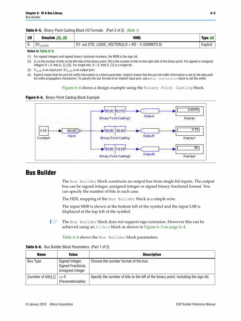
Chapter 6: IO & Bus Library 6–5Bus Builder
Figure 6–4 shows a design example using the Binary Point Casting block.
Bus BuilderThe Bus Builder block constructs an output bus from single-bit inputs. The output bus can be signed integer, unsigned integer or signed binary fractional format. You can specify the number of bits in each case.
The HDL mapping of the Bus Builder block is a simple wire.
The input MSB is shown at the bottom left of the symbol and the input LSB is displayed at the top left of the symbol.
1 The Bus Builder block does not support sign extension. However this can be achieved using an AltBus block as shown in Figure 6–3 on page 6–4.
Table 6–6 shows the Bus Builder block parameters.
O O1[LO].[RO] O1: out STD_LOGIC_VECTOR({LO + RO - 1} DOWNTO 0) Explicit
Notes to Table 6–5:
(1) For signed integers and signed binary fractional numbers, the MSB is the sign bit.(2) [L] is the number of bits on the left side of the binary point; [R] is the number of bits on the right side of the binary point. For signed or unsigned
integers R = 0, that is, [L].[0]. For single bits, R = 0, that is, [1] is a single bit.(3) I1[L].[R] is an input port. O1[L].[R] is an output port.(4) Explicit means that the port bit width information is a block parameter. Implicit means that the port bit width information is set by the data path
bit width propagation mechanism. To specify the bus format of an implicit input port, use a Bus Conversion block to set the width.
Table 6–5. Binary Point Casting Block I/O Formats (Part 2 of 2) (Note 1)
I/O Simulink (2), (3) VHDL Type (4)
Figure 6–4. Binary Point Casting Block Example
Table 6–6. Bus Builder Block Parameters (Part 1 of 2)
Name Value Description
Bus Type Signed Integer, Signed Fractional, Unsigned Integer
Choose the number format of the bus.
[number of bits].[] >= 0 (Parameterizable)
Specify the number of bits to the left of the binary point, including the sign bit.
© January 2010 Altera Corporation DSP Builder Reference Manual

6–6 Chapter 6: IO & Bus LibraryBus Builder
Table 6–7 shows the Bus Builder block I/O formats.
Figure 6–5 shows a design example using the Bus Builder block.
[].[number of bits] >= 0 (Parameterizable)
Specify the number of bits to the right of the binary point. This parameter applies only to signed binary fractional buses.
Table 6–6. Bus Builder Block Parameters (Part 2 of 2)
Name Value Description
Table 6–7. Bus Builder Block I/O Formats (Note 1)
I/O Simulink (2), (3) VHDL Type (4)
I I1[1]
…
Ii[1]
….
In[1]
I1: in STD_LOGIC
…
Ii: in STD_LOGIC
….
In: in STD_LOGIC
Explicit
...
Explicit
...
Explicit
O O1[LP].[RP] with LP + RP = n
where n is the number of inputs
O1: out STD_LOGIC_VECTOR({LP + RP - 1} DOWNTO 0) Explicit
Notes to Table 6–7:
(1) For signed integers and signed binary fractional numbers, the MSB is the sign bit.(2) [L] is the number of bits on the left side of the binary point; [R] is the number of bits on the right side of the binary point. For signed or unsigned
integers R = 0, that is, [L].[0]. For single bits, R = 0, that is, [1] is a single bit.(3) I1[L].[R] is an input port. O1[L].[R] is an output port.(4) Explicit means that the port bit width information is a block parameter. Implicit means that the port bit width information is set by the data path
bit width propagation mechanism. To specify the bus format of an implicit input port, use a Bus Conversion block to set the width.
Figure 6–5. Bus Builder Block Example
DSP Builder Reference Manual © January 2010 Altera Corporation

Chapter 6: IO & Bus Library 6–7Bus Concatenation
Bus ConcatenationThe Bus Concatenation block concatenates two buses.
The block has two inputs, a and b. These may be signed integer or unsigned integer. The output width is width(a) + width(b).
Input a becomes the MSB part of the output, input b becomes the LSB part.
Table 6–8 shows the Bus Concatenation block parameters.
Table 6–9 shows the Bus Concatenation block I/O formats.
Figure 6–6 shows an example using the Bus Concatenation block.
Table 6–8. Bus Concatenation Block Parameters
Name Value Description
Output Is Signed On or Off Turn on if the output bus is signed.
Width of Input a >= 1 (Parameterizable)
Specify the width of the first bus to concatenate.
Width of Input b >= 1 (Parameterizable)
Specify the width of the second bus to concatenate.
Table 6–9. Bus Concatenation Block I/O Formats (Note 1)
I/O Simulink (2), (3) VHDL Type (4)
I I1[N1]
I2[N2]
I1: in STD_LOGIC_VECTOR({N1 - 1} DOWNTO 0)
I2: in STD_LOGIC_VECTOR({N2 - 1} DOWNTO 0)
Explicit
O O1[N1 + N2] O1: out STD_LOGIC_VECTOR({N1 + N2 - 1} DOWNTO 0) Explicit
Notes to Table 6–9:
(1) For signed integers, the MSB is the sign bit.(2) [N] is the number of bits.(3) I1[N] is an input port. O1[N] is an output port.(4) Explicit means that the port bit width information is a block parameter.
Figure 6–6. Bus Concatenation Block Example
© January 2010 Altera Corporation DSP Builder Reference Manual

6–8 Chapter 6: IO & Bus LibraryBus Conversion
Bus ConversionThe Bus Conversion blocextracts a subsection of a bus including bus type and width conversion. If the input is in signed binary fractional format, you should specify a left bit width (number of integer bits) and a right bit width (number of fractional bits) for the output bus. If the input is an integer, you should instead specify which input bit to connect to the output LSB.
1 If Input Bit Connected To Output LSB is on, the input bit indexng starts from 0. This option cannot be used with signed fractional type or in conjunction with rounding.
Table 6–10 shows the Bus Conversion block parameters.
Table 6–11 shows the Bus Conversion block I/O formats.
Table 6–10. Bus Conversion Block Parameters
Name Value Description
Bus Type Signed Integer, Signed Fractional, Unsigned Integer
Choose the input bus type for the simulator, VHDL or both.
Input [number of bits].[] >= 0 (Parameterizable)
Specify the number of bits to the left of the binary point including the sign bit.
Input [].[number of bits] >= 0 (Parameterizable)
Specify the number of bits to the right of the binary point. This parameter applies only to signed binary fractional buses.
Output [number of bits].[] >= 0 (Parameterizable)
Specify the number of bits to the left of the binary point.
Output [].[number of bits] >= 0 (Parameterizable)
Specify the number of bit on the right side of the binary point. This parameter applies only to signed binary fractional buses.
Input Bit Connected to Output LSB
>= 0 (Parameterizable)
Specify which slice of the input bus to use. This parameter designates the start point of the slice which is transferred to the output LSB and applies to signed or unsigned integer buses only.
Round On or Off Turn on to round the output away from zero. When this option is off, the LSM is truncated: <int>(input +0.5).
Saturate On or Off When this option is on, if the output is greater than the maximum positive or negative value to be represented, the output is forced (or saturated) to the maximum positive or negative value, respectively. If off, the MSB is truncated.
Table 6–11. Bus Conversion Block I/O Formats (Note 1)
I/O Simulink (2), (3) VHDL Type (4)
I I1[LPi].[RPi] I1: in STD_LOGIC_VECTOR({LPi + RPi - 1} DOWNTO 0) Explicit
O O1[LPO].[RPO] O1: out STD_LOGIC_VECTOR({LPO + LPO - 1} DOWNTO 0) Explicit
Notes to Table 6–11:
(1) For signed integers and signed binary fractional numbers, the MSB is the sign bit.(2) [L] is the number of bits on the left side of the binary point; [R] is the number of bits on the right side of the binary point. For signed or unsigned
integers R = 0, that is, [L].[0]. For single bits, R = 0, that is, [1] is a single bit.(3) I1[L].[R] is an input port. O1[L].[R] is an output port.(4) Explicit means that the port bit width information is a block parameter. Implicit means that the port bit width information is set by the data path
bit width propagation mechanism. To specify the bus format of an implicit input port, use a Bus Conversion block to set the width.
DSP Builder Reference Manual © January 2010 Altera Corporation

Chapter 6: IO & Bus Library 6–9Bus Splitter
Figure 6–7 shows a design example using the Bus Conversion block.
Bus SplitterThe Bus Splitter block splits a bus into single-bit outputs.
The output ports are numbered from least significant to most significant bit. You can choose the bus type that you wish to use, and specify the number of bits on either side of the binary point.
Table 6–12 shows the Bus Splitter block parameters.
Table 6–13 shows the Bus Splitter block I/O formats.
Figure 6–7. Bus Conversion Block Example
Table 6–12. Bus Splitter Block Parameters
Name Value Description
Bus Type Signed Integer, Signed Fractional, Unsigned Integer
Choose the number format of the bus.
[number of bits].[] >= 0 (Parameterizable)
Specify the number of bits to the left of the binary point, including the sign bit.
[].[number of bits] >= 0 (Parameterizable)
Specify the number of bits to the right of the binary point. This parameter applies only to signed binary fractional buses.
Table 6–13. Bus Splitter Block I/O Formats (Part 1 of 2) (Note 1)
I/O Simulink (2), (3) VHDL Type (4)
I I1[LP].[RP] with LP + RP = n
where n is the number of inputs
I1: in STD_LOGIC_VECTOR({LP + RP - 1} DOWNTO 0) Explicit
© January 2010 Altera Corporation DSP Builder Reference Manual

6–10 Chapter 6: IO & Bus LibraryConstant
Figure 6–8 shows a design example using the Bus Splitter block.
ConstantThe Constant block specifies a constant bus. The options available depend on the selected bus type.
Table 6–14 shows the Constant block parameters.
O O1[1]
…
On[1]
O1: in STD_LOGIC
…
On: in STD_LOGIC
Explicit
...
Explicit
Notes to Table 6–7:
(1) For signed integers and signed binary fractional numbers, the MSB is the sign bit.(2) [L] is the number of bits on the left side of the binary point; [R] is the number of bits on the right side of the binary point. For signed or unsigned
integers R = 0, that is, [L].[0]. For single bits, R = 0, that is, [1] is a single bit.(3) I1[L].[R] is an input port. O1[L].[R] is an output port.(4) Explicit means that the port bit width information is a block parameter. Implicit means that the port bit width information is set by the data path
bit width propagation mechanism. To specify the bus format of an implicit input port, use a Bus Conversion block to set the width.
Table 6–13. Bus Splitter Block I/O Formats (Part 2 of 2) (Note 1)
I/O Simulink (2), (3) VHDL Type (4)
Figure 6–8. Bus Splitter Block Example
Table 6–14. Constant Block Parameters (Part 1 of 2)
Name Value Description
Constant Value Double (Parameterizable)
Specify the constant value that will be formatted with the specified bus type.
Bus Type Signed Integer, Signed Fractional, Unsigned Integer, Single Bit
Choose the number format of the bus.
[number of bits].[] >= 0 (Parameterizable) Specify the number of bits to the left of the binary point, including the sign bit. This parameter does not apply to single-bit buses.
[].[number of bits] >= 0 (Parameterizable) Specify the number of bits to the right of the binary point. This parameter applies only to signed fractional buses.
DSP Builder Reference Manual © January 2010 Altera Corporation

Chapter 6: IO & Bus Library 6–11Constant
Table 6–15 shows the Constant block I/O formats.
Figure 6–9 shows an example using the Constant block.
Rounding Mode Truncate, Round Towards Zero, Round Away From Zero, Round To Plus Infinity, Convergent Rounding
Choose the rounding mode. Refer to the description of the Round block for more information about the rounding modes.
Saturation Mode Wrap, Saturate Choose the saturation mode.
Specify Clock On or Off Turn on to explicitly specify the clock name.
Clock User defined (Parameterizable)
Specify the name of the required clock signal.
Table 6–14. Constant Block Parameters (Part 2 of 2)
Name Value Description
Table 6–15. Constant Block I/O Formats (Note 1)
I/O Simulink (2), (3) VHDL Type (4)
O O1[LP].[RP] O1: out STD_LOGIC_VECTOR({LP + RP - 1} DOWNTO 0) Explicit
Notes to Table 6–15:
(1) For signed integers and signed binary fractional numbers, the MSB is the sign bit.(2) [L] is the number of bits on the left side of the binary point; [R] is the number of bits on the right side of the binary point. For signed or unsigned
integers R = 0, that is, [L].[0]. For single bits, R = 0, that is, [1] is a single bit.(3) I1[L].[R] is an input port. O1[L].[R] is an output port.(4) Explicit means that the port bit width information is a block parameter. Implicit means that the port bit width information is set by the data path
bit width propagation mechanism. To specify the bus format of an implicit input port, use a Bus Conversion block to set the width.
Figure 6–9. Constant Block Example
© January 2010 Altera Corporation DSP Builder Reference Manual

6–12 Chapter 6: IO & Bus LibraryExtract Bit
Extract BitThe Extract Bit block reads a Simulink bus in the specified format and outputs the single bit specified.
The selected bit is indexed starting from zero for the LSB and increasing to (total bit width - 1) for the MSB.
Table 6–16 shows the Extract Bit block parameters.
Table 6–17 shows the Extract Bit block I/O formats.
Figure 6–10 shows a design example using the Extract Bit block.
Table 6–16. Extract Bit Block Parameters
Name Value Description
Bus Type Signed Integer, Signed Fractional, Unsigned Integer
Choose the number format of the bus.
[number of bits].[] >= 0 (Parameterizable) Specify the number of bits to the left of the binary point, including the sign bit.
[].[number of bits] >= 0 (Parameterizable) Specify the number of bits to the right of the binary point.
Select the Bit to be Extracted From the Bus
>= 0 (Parameterizable) Specify which input bit to extract.
Table 6–17. Extract Bit Block I/O Formats (Note 1)
I/O Simulink (2), (3) VHDL Type (4)
I I1[L1].[R1] I1: in STD_LOGIC_VECTOR({L1 + R1 - 1} DOWNTO 0) Explicit
O O1[1] O1: out STD_LOGIC Explicit
Notes to Table 6–17:
(1) For signed integers and signed binary fractional numbers, the MSB is the sign bit.(2) [L] is the number of bits on the left side of the binary point; [R] is the number of bits on the right side of the binary point. For signed or unsigned
integers R = 0, that is, [L].[0]. For single bits, R = 0, that is, [1] is a single bit.(3) I1[L].[R] is an input port. O1[L].[R] is an output port.(4) Explicit means that the port bit width information is a block parameter. Implicit means that the port bit width information is set by the data path
bit width propagation mechanism. To specify the bus format of an implicit input port, use a Bus Conversion block to set the width.
Figure 6–10. Extract Bit Block Example
DSP Builder Reference Manual © January 2010 Altera Corporation

Chapter 6: IO & Bus Library 6–13Global Reset
Global ResetThe Global Reset (or SCLR) block provides a single bit reset signal. All signals driven by the block are connected to the global reset for that clock domain. In simulation, this block outputs a constant 0.
Table 6–18 shows the Global Reset block parameters.
Table 6–19 shows the Global Reset block I/O formats.
GNDThe GND block is a single bit that outputs a constant 0. Table 6–20 shows the GND block parameters.
Table 6–21 shows the GND block I/O formats.
Figure 6–11 shows a design example using the GND block.
Table 6–18. Global Reset Block Parameters
Name Value Description
Specify Clock On or Off Turn on to explicitly specify the clock name.
Clock User defined (Parameterizable) Specify the name of the required clock signal.
Table 6–19. Global Reset Block I/O Formats (Note 1)
I/O Simulink (2), (3) VHDL Type (4)
O O1[1].[0] O1: out STD_LOGIC Explicit
Notes to Table 6–19:
(1) For signed integers and signed binary fractional numbers, the MSB is the sign bit.(2) [L] is the number of bits on the left side of the binary point; [R] is the number of bits on the right side of the binary point. For signed or unsigned
integers R = 0, that is, [L].[0]. For single bits, R = 0, that is, [1] is a single bit.(3) I1[L].[R] is an input port. O1[L].[R] is an output port.(4) Explicit means that the port bit width information is a block parameter. Implicit means that the port bit width information is set by the data path
bit width propagation mechanism. To specify the bus format of an implicit input port, use a Bus Conversion block to set the width.
Table 6–20. GND Block Parameters
Name Value Description
Specify Clock On or Off Turn on to explicitly specify the clock name.
Clock User defined (Parameterizable) Specify the name of the required clock signal.
Table 6–21. GND Block I/O Formats (Note 1)
I/O Simulink (2), (3) VHDL Type (4)
O O1[1].[0] O1: out STD_LOGIC Explicit
Notes to Table 6–21:
(1) For signed integers and signed binary fractional numbers, the MSB is the sign bit.(2) [L] is the number of bits on the left side of the binary point; [R] is the number of bits on the right side of the binary point. For signed or unsigned
integers R = 0, that is, [L].[0]. For single bits, R = 0, that is, [1] is a single bit.(3) I1[L].[R] is an input port. O1[L].[R] is an output port.(4) Explicit means that the port bit width information is a block parameter. Implicit means that the port bit width information is set by the data path
bit width propagation mechanism. To specify the bus format of an implicit input port, use a Bus Conversion block to set the width.
© January 2010 Altera Corporation DSP Builder Reference Manual

6–14 Chapter 6: IO & Bus LibraryInput
InputThe Input block defines the input boundary of a hardware system and casts floating-point Simulink signals (from generic Simulink blocks) to signed binary fractional format (feeding DSP Builder blocks).
Table 6–22 shows the Input block parameters.
Table 6–23 on page 6–15 shows the Input block I/O formats.
Figure 6–11. GND Block Example
Table 6–22. Input Block Parameters
Name Value Description
Bus Type Signed Integer, Signed Fractional, Unsigned Integer, Single Bit
Choose the number format of the bus.
[number of bits].[] >= 0 (Parameterizable)
Specify the number of bits to the left of the binary point, including the sign bit. This parameter does not apply to single-bit buses.
[].[number of bits] >= 0 (Parameterizable)
Specify the number of bits to the right of the binary point. This parameter applies only to signed fractional buses.
Specify Clock On or Off Turn on to explicitly specify the clock name.
Clock User defined (Parameterizable)
Specify the name of the required clock signal.
DSP Builder Reference Manual © January 2010 Altera Corporation
Chapter 6: IO & Bus Library 6–15Non-synthesizable Input
Non-synthesizable InputThe Non-synthesizable Input block marks an entry point to a non-synthesizable DSP Builder system. Use a corresponding Non-synthesizable Output block to mark the exit point. Because DSP Builder registers its own type with Simulink, this block is required when the DSP Builder blocks are not intended to be synthesized.
Table 6–24 shows the Non-synthesizable Input block parameters.
Table 6–25 shows the Non-synthesizable Input block I/O formats.
Table 6–23. Input Block I/O Formats (Note 1)
I/O Simulink (2), (3) VHDL Type (4)
I I1[L1].[R1] I1: out STD_LOGIC_VECTOR({L1 + R1 - 1} DOWNTO 0) Implicit - Optional
O O1[LP].[RP] O1: out STD_LOGIC_VECTOR({LP + RP - 1} DOWNTO 0) Explicit
Notes to Table 6–23:
(1) For signed integers and signed binary fractional numbers, the MSB is the sign bit.(2) [L] is the number of bits on the left side of the binary point; [R] is the number of bits on the right side of the binary point. For signed or unsigned
integers R = 0, that is, [L].[0]. For single bits, R = 0, that is, [1] is a single bit.(3) I1[L].[R] is an input port. O1[L].[R] is an output port.(4) Explicit means that the port bit width information is a block parameter. Implicit means that the port bit width information is set by the data path
bit width propagation mechanism. To specify the bus format of an implicit input port, use a Bus Conversion block to set the width.
Table 6–24. Non-synthesizable Input Block Parameters
Name Value Description
Bus Type Signed Integer, Signed Fractional, Unsigned Integer, Single Bit
Choose the number format of the bus.
[number of bits].[] >= 0 (Parameterizable)
Specify the number of bits to the left of the binary point, including the sign bit. This parameter does not apply to single-bit buses.
[].[number of bits] >= 0 (Parameterizable)
Specify the number of bits to the right of the binary point. This parameter applies only to signed fractional buses.
Specify Clock On or Off Turn on to explicitly specify the clock name.
Clock User defined (Parameterizable)
Specify the name of the required clock signal.
Table 6–25. Non-synthesizable Input Block I/O Formats (Note 1)
I/O Simulink (2), (3) VHDL Type (4)
I I1[L1].[R1] I1: out STD_LOGIC_VECTOR({L1 + R1 - 1} DOWNTO 0) Implicit - Optional
O O1[LP].[RP] O1: out STD_LOGIC_VECTOR({LP + RP - 1} DOWNTO 0) Explicit
Notes to Table 6–23:
(1) For signed integers and signed binary fractional numbers, the MSB is the sign bit.(2) [L] is the number of bits on the left side of the binary point; [R] is the number of bits on the right side of the binary point. For signed or unsigned
integers R = 0, that is, [L].[0]. For single bits, R = 0, that is, [1] is a single bit.(3) I1[L].[R] is an input port. O1[L].[R] is an output port.(4) Explicit means that the port bit width information is a block parameter. Implicit means that the port bit width information is set by the data path
bit width propagation mechanism. To specify the bus format of an implicit input port, use a Bus Conversion block to set the width.
© January 2010 Altera Corporation DSP Builder Reference Manual

6–16 Chapter 6: IO & Bus LibraryNon-synthesizable Output
Non-synthesizable OutputThe Non-synthesizable Output block marks an exit point from a non-synthesizable DSP Builder system. Use a corresponding Non-synthesizable Input block to mark the entry point. Because DSP Builder registers its own type with Simulink, this block is required when the DSP Builder blocks are not intended to be synthesized. You can also use this block to create an non-synthesizable output from a synthesizable system.
You can optionally specify the external Simulink type. If set to Simulink Fixed Point Type, the bit width is the same as the DSP Builder input type. If set to Double, the width may be truncated if the bit width is greater than 52.
Table 6–26 shows the Non-synthesizable Output block parameters.
Table 6–27 shows the Non-synthesizable Output block I/O formats.
Table 6–26. Non-synthesizable Output Block Parameters
Name Value Description
Bus Type Inferred, Signed Integer, Unsigned Integer, Signed Fractional, Single Bit
Choose the number format of the bus.
[number of bits].[] >= 0 (Parameterizable) Specify the number of bits to the left of the binary point, including the sign bit. This parameter does not apply to single-bit buses.
[].[number of bits] >= 0 (Parameterizable) Specify the number of bits to the right of the binary point. This parameter applies only to signed fractional buses.
External Type Inferred, Simulink Fixed Point Type, Double
Specifies whether the external type is inferred from the Simulink block it is connected to or explicitly set to either Simulink Fixed Point or Double type. The default is Inferred.
Table 6–27. Non-synthesizable Output Block I/O Formats (Note 1)
I/O Simulink (2), (3) VHDL Type (4)
I I1[L1].[R1] I1: out STD_LOGIC_VECTOR({L1 + R1 - 1} DOWNTO 0) Implicit - Optional
O O1[LP].[RP] O1: out STD_LOGIC_VECTOR({LP + RP - 1} DOWNTO 0) Explicit
Notes to Table 6–29:
(1) For signed integers and signed binary fractional numbers, the MSB is the sign bit.(2) [L] is the number of bits on the left side of the binary point; [R] is the number of bits on the right side of the binary point. For signed or unsigned
integers R = 0, that is, [L].[0]. For single bits, R = 0, that is, [1] is a single bit.(3) I1[L].[R] is an input port. O1[L].[R] is an output port.(4) Explicit means that the port bit width information is a block parameter. Implicit means that the port bit width information is set by the data path
bit width propagation mechanism. To specify the bus format of an implicit input port, use a Bus Conversion block to set the width.
DSP Builder Reference Manual © January 2010 Altera Corporation

Chapter 6: IO & Bus Library 6–17Output
OutputThe Output block defines the output boundary of a hardware system and casts signed binary fractional format (from DSP Builder blocks) to floating-point Simulink signals (feeding generic Simulink blocks).
Output blocks map to output ports in VHDL and mark the edge of the generated system. You would normally connect these blocks to Simulink simulation blocks in your testbench. Their outputs should not be connected to other Altera blocks.
You can optionally specify the external Simulink type. If set to Simulink Fixed Point Type, the bit width is the same as the input. If set to Double, the width may be truncated if the bit width is greater than 52.
Table 6–28 shows the Output block parameters.
Table 6–29 shows the Output block I/O formats.
Table 6–28. Output Block Parameters
Name Value Description
Bus Type Inferred, Signed Integer, Unsigned Integer, Signed Fractional, Single Bit
Choose the number format of the bus.
[number of bits].[] >= 0 (Parameterizable) Specify the number of bits to the left of the binary point, including the sign bit. This parameter does not apply to single-bit buses.
[].[number of bits] >= 0 (Parameterizable) Specify the number of bits to the right of the binary point. This parameter applies only to signed fractional buses.
External Type Inferred, Simulink Fixed Point Type, Double
Specifies whether the external type is inferred from the Simulink block it is connected to or explicitly set to either Simulink Fixed Point or Double type. The default is Inferred.
Table 6–29. Output Block I/O Formats (Note 1)
I/O Simulink (2), (3) VHDL Type (4)
I I1[L1].[R1] I1: out STD_LOGIC_VECTOR({L1 + R1 - 1} DOWNTO 0) Implicit - Optional
O O1[LP].[RP] O1: out STD_LOGIC_VECTOR({LP + RP - 1} DOWNTO 0) Explicit
Notes to Table 6–29:
(1) For signed integers and signed binary fractional numbers, the MSB is the sign bit.(2) [L] is the number of bits on the left side of the binary point; [R] is the number of bits on the right side of the binary point. For signed or unsigned
integers R = 0, that is, [L].[0]. For single bits, R = 0, that is, [1] is a single bit.(3) I1[L].[R] is an input port. O1[L].[R] is an output port.(4) Explicit means that the port bit width information is a block parameter. Implicit means that the port bit width information is set by the data path
bit width propagation mechanism. To specify the bus format of an implicit input port, use a Bus Conversion block to set the width.
© January 2010 Altera Corporation DSP Builder Reference Manual

6–18 Chapter 6: IO & Bus LibraryRound
RoundThe Round block rounds the input to the closest possible representation in the specified output bus format. If the nearest two possibilities are equidistant, you can choose from the available rounding modes:
■ Truncate: Remove discarded bits without changing the other bits; effectively, choose the lower value. This is the simplest and fastest mode to implement in hardware.
■ Round Towards Zero: Choose the value closer to zero.
■ Round Away From Zero: Choose the value further from zero (round downwards for negative values, upwards for positive values). This was the rounding behavior in DSP Builder version 7.0 and before. Care should be taken when using this mode —the maximum positive value will overflow the available representation. For example, when rounding from an 8-bit signed input to a 6-bit signed output, 01111111 (127) becomes 100000 (-32). If you use this mode, it is best to use saturation logic to prevent this from happening.
■ Round To Plus Infinity: Choose the higher value.
■ Convergent Rounding: Choose the even value. This mode has the advantage that for a large sample of random input values there is no bias —on average the same number of values round upwards as downwards.
1 When using Simulink fixed-point types, MATLAB supports the following rounding options: Zero, Nearest (equivalent to Round Away From Zero), Ceiling, Floor (equivalent to Truncate), and Simplest. The MATLAB Zero and Ceiling modes round all intermediate values up or down and have no DSP Builder equivalent. This is because the DSP Builder modes (except Truncate) always choose the nearest representable value and the rounding mode applies only to values that are equidistant from two representable values. For example, 0.9 rounds to 1 (for all modes except Truncate) but the MATLAB Zero mode rounds 0.9 to 0. Similarly 0.1 rounds to 0 but the MATLAB Ceiling mode rounds 0.1 to 1.
Table 6–30 shows the Round block parameters.
Table 6–30. Round Block Parameters (Part 1 of 2)
Name Value Description
Bus Type Signed Integer, Signed Fractional, Unsigned Integer
Choose the number format of the bus.
[number of bits].[] >= 2 (Parameterizable) Specify the number of bits to the left of the binary point, including the sign bit. This parameter does not apply to single-bit buses.
[].[number of bits] >= 0 (Parameterizable) Specify the number of bits to the right of the binary point. This parameter applies only to signed fractional buses.
Number of LSB Bits to Remove
>= 0 (Parameterizable) Specify how many bits to remove.
DSP Builder Reference Manual © January 2010 Altera Corporation

Chapter 6: IO & Bus Library 6–19Round
Table 6–31 shows the Round block I/O formats.
Figure 6–12 shows a design example using the Round block.
Rounding Mode Truncate, Round Towards Zero, Round Away From Zero, Round To Plus Infinity, Convergent Rounding
Choose the rounding mode.
Enable Pipeline On or Off Turn on if you would like to pipeline the function.
Use Enable Port (1) On or Off Turn on to use the clock enable input (ena).
Use Asynchronous Clear Port (1)
On or Off Turn on to use the asynchronous clear input (aclr).
Note to Table 6–30:
(1) These ports are available only when pipeline is enabled.
Table 6–30. Round Block Parameters (Part 2 of 2)
Name Value Description
Table 6–31. Round Block I/O Formats (Note 1)
I/O Simulink (2), (3) VHDL Type (4)
I I1[L1].[R1]
I2[1]
I3[1]
I1: out STD_LOGIC_VECTOR({L1 + R1 - 1} DOWNTO 0)
I2: in STD_LOGIC
I3: in STD_LOGIC
Explicit
O O1[LP].[RP] O1: out STD_LOGIC_VECTOR({LP + RP - 1} DOWNTO 0) Explicit
Notes to Table 6–31:
(1) For signed integers and signed binary fractional numbers, the MSB is the sign bit.(2) [L] is the number of bits on the left side of the binary point; [R] is the number of bits on the right side of the binary point. For signed or unsigned
integers R = 0, that is, [L].[0]. For single bits, R = 0, that is, [1] is a single bit.(3) I1[L].[R] is an input port. O1[L].[R] is an output port.(4) Explicit means that the port bit width information is a block parameter. Implicit means that the port bit width information is set by the data path
bit width propagation mechanism. To specify the bus format of an implicit input port, use a Bus Conversion block to set the width.
Figure 6–12. Round Block Example
© January 2010 Altera Corporation DSP Builder Reference Manual

6–20 Chapter 6: IO & Bus LibrarySaturate
SaturateThe Saturate block block limits output to a maximum value. If the output is greater than the maximum positive or negative value to be represented, the output is forced (or saturated) to the maximum positive or negative value, respectively. Alternatively, you can choose to truncate the MSB.
Table 6–32 shows the Saturate block parameters.
Table 6–32. Saturate Block Parameters
Name Value Description
Input Bus Type Signed Integer, Signed Fractional, Unsigned Integer
Choose the number format of the bus.
[number of bits].[] >= 2 (Parameterizable) Specify the number of bits to the left of the binary point, including the sign bit. This parameter does not apply to single-bit buses.
[].[number of bits] >= 0 (Parameterizable) Specify the number of bits to the right of the binary point. This parameter applies only to signed fractional buses.
Number of MSB Bits to Remove
>= 0 (Parameterizable) Specify how many bits to remove.
Saturation Type Saturate, Truncate MSB, Enter Saturation Limits
Choose whether to saturate, truncate, or specify the saturation limits for the output.
Upper Saturation Limit Integer (Parameterizable)
Specify the upper saturation limit when Saturation Type is set to Enter Saturation Limits.
Lower Saturation Limit Integer (Parameterizable)
Specify the lower saturation limit when Saturation Type is set to Enter Saturation Limits.
Enable Pipeline On or Off Turn on if you would like to pipeline the function.
Use Saturation Occurred Port
On or Off Turn on to use the saturation occurred input (sat_flag).
Use Enable Port (1) On or Off Turn on to use the clock enable input (ena).
Use Asynchronous Clear Port (1)
On or Off Turn on to use the asynchronous clear input (aclr).
Note to Table 6–30:
(1) These ports are available only when pipeline is enabled.
DSP Builder Reference Manual © January 2010 Altera Corporation

Chapter 6: IO & Bus Library 6–21VCC
Table 6–33 shows the Saturate block I/O formats.
Figure 6–13 shows a design example using the Saturate block.
VCCThe VCC block outputs a single-bit constant 1.
Table 6–34 shows the VCC block parameters.
Table 6–33. Saturate Block I/O Formats (Note 1)
I/O Simulink (2), (3) VHDL Type (4)
I I1[L1].[R1]
I2[1]
I3[1]
I4[1]
I1: out STD_LOGIC_VECTOR({L1 + R1 - 1} DOWNTO 0)
I2: in STD_LOGIC
I3: in STD_LOGIC
I4: in STD_LOGIC
Explicit
O O1[LP].[RP] O1: out STD_LOGIC_VECTOR({LP + RP - 1} DOWNTO 0) Explicit
Notes to Table 6–33:
(1) For signed integers and signed binary fractional numbers, the MSB is the sign bit.(2) [L] is the number of bits on the left side of the binary point; [R] is the number of bits on the right side of the binary point. For signed or unsigned
integers R = 0, that is, [L].[0]. For single bits, R = 0, that is, [1] is a single bit.(3) I1[L].[R] is an input port. O1[L].[R] is an output port.(4) Explicit means that the port bit width information is a block parameter. Implicit means that the port bit width information is set by the data path
bit width propagation mechanism. To specify the bus format of an implicit input port, use a Bus Conversion block to set the width.
Figure 6–13. Saturate Block Example
Table 6–34. VCC Block Parameters
Name Value Description
Specify Clock On or Off Turn on to explicitly specify the clock name.
Clock User defined (Parameterizable)
Specify the name of the required clock signal.
© January 2010 Altera Corporation DSP Builder Reference Manual

6–22 Chapter 6: IO & Bus LibraryVCC
Table 6–35 shows the VCC block I/O formats.
Figure 6–14 shows a design example using the VCC block.
Table 6–35. VCC Block I/O Formats (Note 1)
I/O Simulink (2), (3) VHDL Type (4)
O O1[1] O1: out STD_LOGIC Explicit
Notes to Table 6–35:
(1) For signed integers and signed binary fractional numbers, the MSB is the sign bit.(2) [L] is the number of bits on the left side of the binary point; [R] is the number of bits on the right side of the binary point. For signed or unsigned
integers R = 0, that is, [L].[0]. For single bits, R = 0, that is, [1] is a single bit.(3) I1[L].[R] is an input port. O1[L].[R] is an output port.(4) Explicit means that the port bit width information is a block parameter. Implicit means that the port bit width information is set by the data path
bit width propagation mechanism. To specify the bus format of an implicit input port, use a Bus Conversion block to set the width.
Figure 6–14. VCC Block Example
DSP Builder Reference Manual © January 2010 Altera Corporation

© January 2010 Altera Corporation
7. Rate Change Library
The Rate Change library contains the following blocks that allow you to control the clock assignment to registered DSP Builder blocks, such as Delay or Increment Decrement blocks:
■ Clock
■ Clock_Derived
■ Dual-Clock FIFO
■ Multi-Rate DFF
■ PLL
■ Tsamp
For information about the Clock and Clock_Derived blocks, refer to Chapter 1, AltLab Library. For information about the Dual-Clock FIFO block , refer to Chapter 9, Storage Library.
Multi-Rate DFFThe Multi-Rate DFF block implements a D-type flipflop and is typically used to specify sample rate transitions.
1 Simulation of the Multi-Rate DFF block may not match hardware because of limitations in the way DSP Builder simulates multi-clock designs. Typically, differences may occur when moving from a slow to a fast clock domain. In such cases, an error message of the following form is issued in the MATLAB command window:
Warning: simulation will not match hardware
If your design allows, increasing the latency of the Multi-Rate DFF block to at least one slow clock period should result in correct simulation results.
If the clocks are asynchronous, simulations will not match hardware. Using a Multi-Rate DFF block to cross asynchronous clock domains is likely to result in data being corrupted or lost. Use a Dual-Clock FIFO block instead to guarantee correct data transfer.
The Multi-Rate DFF block has the inputs and outputs shown in Table 7–1.
Table 7–1. Multi-Rate DFF Block Inputs and Outputs
Signal Direction Description
d Input Input data port.
q Output Output data port.
ena Input Optional clock enable port.
sclr Input Optional synchronous clear port.
DSP Builder Reference Manual
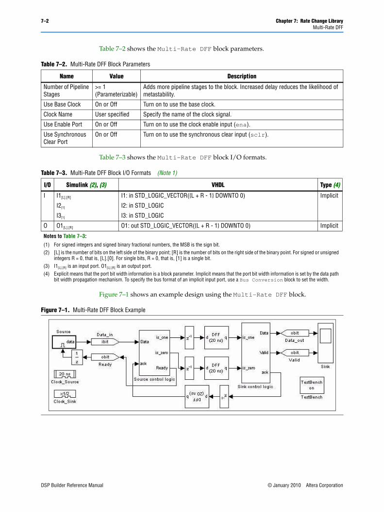
7–2 Chapter 7: Rate Change LibraryMulti-Rate DFF
Table 7–2 shows the Multi-Rate DFF block parameters.
Table 7–3 shows the Multi-Rate DFF block I/O formats.
Figure 7–1 shows an example design using the Multi-Rate DFF block.
Table 7–2. Multi-Rate DFF Block Parameters
Name Value Description
Number of Pipeline Stages
>= 1 (Parameterizable)
Adds more pipeline stages to the block. Increased delay reduces the likelihood of metastability.
Use Base Clock On or Off Turn on to use the base clock.
Clock Name User specified Specify the name of the clock signal.
Use Enable Port On or Off Turn on to use the clock enable input (ena).
Use Synchronous Clear Port
On or Off Turn on to use the synchronous clear input (sclr).
Table 7–3. Multi-Rate DFF Block I/O Formats (Note 1)
I/O Simulink (2), (3) VHDL Type (4)
I I1[L].[R]
I2[1]
I3[1]
I1: in STD_LOGIC_VECTOR({L + R - 1} DOWNTO 0)
I2: in STD_LOGIC
I3: in STD_LOGIC
Implicit
O O1[L].[R] O1: out STD_LOGIC_VECTOR({L + R - 1} DOWNTO 0) Implicit
Notes to Table 7–3:
(1) For signed integers and signed binary fractional numbers, the MSB is the sign bit.(2) [L] is the number of bits on the left side of the binary point; [R] is the number of bits on the right side of the binary point. For signed or unsigned
integers R = 0, that is, [L].[0]. For single bits, R = 0, that is, [1] is a single bit.(3) I1[L].[R] is an input port. O1[L].[R] is an output port.(4) Explicit means that the port bit width information is a block parameter. Implicit means that the port bit width information is set by the data path
bit width propagation mechanism. To specify the bus format of an implicit input port, use a Bus Conversion block to set the width.
Figure 7–1. Multi-Rate DFF Block Example
DSP Builder Reference Manual © January 2010 Altera Corporation

Chapter 7: Rate Change Library 7–3PLL
PLLThe PLL block generates a clock signal that is based on a reference clock.
Phase-locked loops (PLL) have become an important building block of most high-speed digital systems today. Their use ranges from improving timing as zero delay lines to full-system clock synthesis. The Arria, Cyclone, and Stratix series device families offer advanced on-chip PLL features that were previously offered only by the most complex discrete devices.
Each PLL has multiple outputs that can source any of the 40 system clocks in the devices to give you complete control over your clocking needs. The PLLs offer full frequency synthesis capability (the ability to multiply up or divide down the clock period) and phase shifting for optimizing I/O timing. Additionally, the PLLs have high-end features such as programmable bandwidth, spread spectrum, and clock switchover.
The PLL block generates internal clocks with frequencies that are multiples of the frequency of the system clock. PLLs on the FPGA can simultaneously multiply and divide the reference clock. The PLL block checks the validity of the parameters.
1 If you use a PLL block to define clock signals when there is no Clock block in your design, the PLL-derived clocks might not pass the derived period correctly to the blocks referencing the PLL-derived clock. Always explicitly include a Clock block when using a PLL block.
The number of PLL internal clock outputs supported by each device family depends on the specific device packaging.
f For information about the built-in PLLs, refer to the device handbook for the device family you are targeting.
The following restrictions apply when you are using a PLL block:
■ Your design may contain more than one PLL block but they must be at the top level.
■ Each output clock of the PLL has a zero degree phase shift and 50% duty cycle.
Table 7–4 shows the PLL block parameters.
Table 7–4. PLL Block Parameters (Part 1 of 2)
Name Value Description
Input Clock: User specified Specify the name of the input clock signal.
Use Base Clock On or Off Turn on to use the base clock.
Number of Output Clocks 1–9 Choose the number of PLL clock outputs.
Output Clocks <PLL block name>_clk0 to <PLL block name>_clk8
Select the PLL clock that you want to set frequency multiplier and divider factors for.
Period Multiplier (1) Multiply the reference clock period by this value.
Period Divider (1) Divide the reference clock period by this value.
© January 2010 Altera Corporation DSP Builder Reference Manual

7–4 Chapter 7: Rate Change LibraryTsamp
TsampThe Tsamp block sets the clock domain inherited by all downstream blocks.
1 When you use the Tsamp block, you must select a variable step solver in the Simulink configuration parameters. Unless the downstream clock is an exact, slower multiple of the upstream clock, the simulation results may not match ModelSim; in this case it is better to use a Multi-Rate DFF block.
The Tsamp block has the inputs and outputs shown in Table 7–5.
Table 7–6 shows the Tsamp block parameters.
Table 7–7 shows the Tsamp block I/O formats.
Figure 7–2 on page 7–5 shows an example design using the Tsamp block.
Export As Output Pin On or Off Turn on to export this clock as an output pin.
Note to Table 7–4:
(1) Refer to the device documentation for the device family you are targeting.
Table 7–4. PLL Block Parameters (Part 2 of 2)
Name Value Description
Table 7–5. Tsamp Block Inputs and Outputs
Signal Direction Description
<unnamed> Input Input data port.
<unnamed> Output Output data port.
Table 7–6. Tsamp Block Parameters
Name Value Description
Specify Clock On or Off Turn on to explicitly specify the clock name.
Clock Name User specified Specify the name of the Clock block used to specify the clock signal.
Table 7–7. Tsamp Block I/O Formats (Note 1)
I/O Simulink (2), (3) VHDL Type (4)
I I1[L].[R] I1: in STD_LOGIC_VECTOR({L + R - 1} DOWNTO 0) Implicit
O O1[L].[R] O1: out STD_LOGIC_VECTOR({L + R - 1} DOWNTO 0) Implicit
Notes to Table 7–7:
(1) For signed integers and signed binary fractional numbers, the MSB is the sign bit.(2) [L] is the number of bits on the left side of the binary point; [R] is the number of bits on the right side of the binary point. For signed or unsigned
integers R = 0, that is, [L].[0]. For single bits, R = 0, that is, [1] is a single bit.(3) I1[L].[R] is an input port. O1[L].[R] is an output port.(4) Explicit means that the port bit width information is a block parameter. Implicit means that the port bit width information is set by the data path
bit width propagation mechanism. To specify the bus format of an implicit input port, use a Bus Conversion block to set the width.
DSP Builder Reference Manual © January 2010 Altera Corporation

Chapter 7: Rate Change Library 7–5Tsamp
This example design is available in the <DSP Builder install path>\DesignExamples \Demos\Filters\Filters\CicFilter directory.
Figure 7–2. Tsamp Block Example
© January 2010 Altera Corporation DSP Builder Reference Manual

7–6 Chapter 7: Rate Change LibraryTsamp
DSP Builder Reference Manual © January 2010 Altera Corporation

© January 2010 Altera Corporation
8. Simulation Library
The Simulation library contains the following simulation-only blocks that do not synthesize to HDL when Signal Compiler is run:
■ External RAM
■ Multiple Port External RAM
External RAMThe External RAM block is a simulation model of an external RAM. The External RAM block stores and retrieves data from a range of addresses and is compatible with the Avalon-MM interface.
f For information about the Avalon-MM interface, refer to Avalon Interface Specifications.
This block is not cycle-accurate and a warning is issued if you use it in a gate level (cycle-accurate) simulation.
1 If 64 or 128 bit data width is specified, the block attempts to use a Simulink fixed-point license. If you do not have a Simulink fixed-point license., you can only use 8, 16 or 32 bit data widths.
f For information about fixed-point licenses, refer to the Simulink Help.
This is a simulation only block, and does not generate any HDL when Signal Compiler is run.
The External RAM block has the inputs and outputs shown in Table 8–1.
Table 8–1. External RAM Block Inputs and Outputs (Part 1 of 2)
Signal Direction Description
WriteData Input Data lines for write transfers. Not required if there are no write transfers. If used, Write must also be used
WriteAddress Input Address lines for write transfers.
ReadAddress Input Address lines for read transfers.
Read Input Read request signal. Not required if there are no read transfers. If used, ReadData must also be used.
Write Input Write request signal. Not required if there are no write transfers. If used, WriteData must also be used.
ReadData Output Data lines for read transfers. Not required if there are no read transfers. If used, Read must also be used.
WriteWaitRequest Output Used to stall the interface when the Avalon-MM interface is not able to respond immediately to a write request.
DSP Builder Reference Manual

8–2 Chapter 8: Simulation LibraryExternal RAM
Table 8–2 shows the External RAM block parameters.
Figure 8–1 shows an example design using the External RAM block.
ReadWaitRequest Output Used to stall the interface when the Avalon-MM interface is not able to respond immediately to a read request.
ReadDataValid Output Marks the rising clock edge when ReadData is asserted. Indicates that valid data is present on the ReadData lines.
Table 8–1. External RAM Block Inputs and Outputs (Part 2 of 2)
Signal Direction Description
Table 8–2. External RAM Block Parameters
Name Value Description
Data Width 8, 16, 32, 64, or 128
Specifies the number of bits used for the data. No other values are supported. 64 and 128 bit data widths require a Simulink fixed-point license.
Address Width 1–32 Specifies the number of bits n used for the address.
Wait States Per Write 0–10 You can choose a fixed number of wait states for each write transfer.
Maximum Latency 1–255 Specifies the latency for pipelined read transfers.
Size 1–2n (Note 1) Specifies the total size of the RAM in bytes (the number of addresses when you are using a range of addresses).
Offset 1–2n (Note 1) Specifies an offset for the RAM start address (the start address when you are using a range of addresses.
Notes to Table 8–2
(1) The size added to the offset must be less than 2n where n is the address width.
Figure 8–1. External RAM Block Example
DSP Builder Reference Manual © January 2010 Altera Corporation

Chapter 8: Simulation Library 8–3Multiple Port External RAM
Multiple Port External RAMThe Multiple Port External RAM block is a simulation model of a multiple port external RAM block. It stores and retrieves data from a range of addresses and is compatible with the Avalon-MM interface.
f For information about the Avalon-MM interface, refer to Avalon Interface Specifications.
This block is not cycle-accurate and a warning is issued if you use it in a gate level (cycle-accurate) simulation.
1 If 64 or 128 bit data width is specified, the block attempts to use a Simulink fixed-point license. If you do not have a Simulink fixed-point license., you can only use 8, 16 or 32 bit data widths.
f For information about fixed-point licenses, refer to the Simulink Help.
This is a simulation only block, and does not generate any HDL when you run Signal Compiler.
The ports on the block symbol are updated when you change the number of write or read interfaces. However, the port names are not automatically shown on the block symbol. To display the updated block symbol correctly, perform the following steps:
1. Click on the block, point to Link Options in the popup menu and click Break Link.
2. While the block is still selected, run the following command in MATLAB:
alt_dspbuilder_update_external_RAM
The Multiple Port External RAM block has the inputs and outputs shown in Table 8–3.
Table 8–3. Multiple Port External RAM Block Inputs and Outputs
Signal Direction Description
WriteDataN Input Data lines for write transfers on port N.
WriteAddressN Input Address lines for write transfers on port N.
WriteEnableN Input Write enable for transfers on port N.
WriteBurstCountN Input Write burst count for transfers on port N.
ReadAddressN Input Address lines for read transfers on port N.
ReadEnableN Input Read enable for transfers on port N.
ReadBurstCountN Input Read burst count for transfers on port N.
WriteWaitRequestN Output Used to stall the interface when the Avalon-MM interface is not able to respond immediately to a write request on port N.
ReadDataN Output Data lines for read transfers on port N.
ReadDataValidN Output Marks the rising clock edge when ReadDataN is asserted. Indicates that valid data is present on the ReadDataN lines.
ReadWaitRequestN Output Used to stall the interface when the Avalon-MM interface is not able to respond immediately to a read request on port N.
© January 2010 Altera Corporation DSP Builder Reference Manual

8–4 Chapter 8: Simulation LibraryMultiple Port External RAM
Table 8–4 shows the Multiple Port External RAM block parameters.
Table 8–4. Multiple Port External RAM Block Parameters
Name Value Description
Number of Write Interfaces 0–5 Specifies the number of write ports.
Number of Read Interfaces 0–5 Specifies the number of read ports.
Data Width 8, 16, 32, 64, or 128
Specifies the number of bits used for the data. No other values are supported. 64 and 128 bit data widths require a Simulink fixed-point license.
Address Width 1–32 Specifies the number of bits n used for the address.
Wait States Per Write 0–10 You can choose a fixed number of wait states for each write transfer.
Maximum Latency 1–255 Specifies the latency for pipelined read transfers.
Size 1–2n (Note 1) Specifies the total size of the RAM in bytes (the number of addresses when you are using a range of addresses).
Offset 1–2n (Note 1) Specifies an offset for the RAM start address (the start address when you are using a range of addresses.
Notes to Table 8–4
(1) The size added to the offset must be less than 2n where n is the address width.
DSP Builder Reference Manual © January 2010 Altera Corporation

© January 2010 Altera Corporation
9. Storage Library
The Storage library contains the following blocks which support storage and associated control functions:
■ Delay
■ Down Sampling
■ Dual-Clock FIFO
■ Dual-Port RAM
■ FIFO
■ LUT (Look-Up Table)
■ Memory Delay
■ Parallel To Serial
■ ROM
■ Serial To Parallel
■ Shift Taps
■ Single-Port RAM
■ True Dual-Port RAM
■ Up Sampling
DSP Builder Reference Manual

9–2 Chapter 9: Storage LibraryDelay
Delay The Delay block delays the incoming data by an amount specified by the number of pipeline stages. The block accepts any data type as inputs.
The Delay block has the inputs and outputs shown in Table 9–1.
Table 9–2 shows the Delay block parameters.
Table 9–3 shows the Delay block I/O formats.
Table 9–1. Delay Block Inputs and Outputs
Signal Direction Description
<unnamed> Input Input data port.
ena Input Optional clock enable port.
sclr Input Optional synchronous clear port.
<unnamed> Output Output data port.
Table 9–2. Delay Block Parameters
Name Value Description
Number of Pipeline Stages
User Defined (Parameterizable)
Specify the pipeline length of the block. The delay must be greater than or equal to 1.
Clock Phase Selection
User Defined Specify the phase selection with a binary string, where a 1 indicates the phase in which the Delay block is enabled. For example:
1—The block is always enabled and captures all data passing through the block (sampled at the rate 1).
10—The block is enabled every other phase and every other data (sampled at the rate 1) passes through.
0100—The block is enabled on the second phase of and only the second data of (sampled at the rate 1) passes through. That is, the data on phases 1, 3, and 4 do not pass through the delay block.
Use Enable Port On or Off Turn on to use the clock enable input (ena).
Use Synchronous Clear Port
On or Off Turn on to use the synchronous clear input (sclr).
Reset To Constant (Non-Zero) Value
On or Off Turn on to specify a non-zero reset value. Specifying a reset value increases the hardware resources used.
Reset Value User Defined (Parameterizable)
Specify the reset value.
Table 9–3. Delay Block I/O Formats (Part 1 of 2) (Note 1)
I/O Simulink (2), (3) VHDL Type (4)
I I1[L1].[R1]
I2[1]
I3[1]
I1: in STD_LOGIC_VECTOR({L1 + R1 - 1} DOWNTO 0)
I2: in STD_LOGIC
I3: in STD_LOGIC
Implicit
DSP Builder Reference Manual © January 2010 Altera Corporation

Chapter 9: Storage Library 9–3Down Sampling
Figure 9–1 shows an example using the Delay block.
Down SamplingThe Down Sampling block decreases the output sample rate from the input sample rate. The output data is sampled at every Nth cycle where N is the down sampling rate. The output data is then held constant for the next N input cycles.
The Down Sampling block has the inputs and outputs shown in Table 9–4.
Table 9–5 shows the Down Sampling block parameters.
O O1[L1].[R1] O1: in STD_LOGIC_VECTOR({L1 + R1 - 1} DOWNTO 0) Implicit
Notes to Table 9–3:
(1) For signed integers and signed binary fractional numbers, the MSB is the sign bit.(2) [L] is the number of bits on the left side of the binary point; [R] is the number of bits on the right side of the binary point. For signed or unsigned
integers R = 0, that is, [L].[0]. For single bits, R = 0, that is, [1] is a single bit.(3) I1[L].[R] is an input port. O1[L].[R] is an output port.(4) Explicit means that the port bit width information is a block parameter. Implicit means that the port bit width information is set by the data path
bit width propagation mechanism. To specify the bus format of an implicit input port, use a Bus Conversion block to set the width.
Table 9–3. Delay Block I/O Formats (Part 2 of 2) (Note 1)
I/O Simulink (2), (3) VHDL Type (4)
Figure 9–1. Delay Block Example
Table 9–4. Down Sampling Block Inputs and Outputs
Signal Direction Description
d Input Input data port.
q Output Output data port.
Table 9–5. Down Sampling Block Parameters
Name Value Description
Down Sampling Rate An integer greater than 1 (Parameterizable)
Specify the down sampling rate.
© January 2010 Altera Corporation DSP Builder Reference Manual

9–4 Chapter 9: Storage LibraryDual-Clock FIFO
Table 9–6 shows the Down Sampling block I/O formats.
Figure 9–2 shows an example using the Down Sampling block.
Dual-Clock FIFOThe Dual-Clock FIFO block implements a parameterized, dual-clock FIFO buffer controlled by separate read-side and write-side clocks.
1 The Dual-Clock FIFO block simulation in Simulink is functionally equivalent to hardware, but not cycle-accurate.
The Dual-Clock FIFO block has the inputs and outputs shown in Table 9–7.
Table 9–6. Down Sampling Block I/O Formats (Note 1)
I/O Simulink (2), (3) VHDL Type (4)
I I1[L1].[R1] I1: in STD_LOGIC_VECTOR({L1 + R1 - 1} DOWNTO 0) Implicit
O O1[L1].[R1] O1: in STD_LOGIC_VECTOR({L1 + R1 - 1} DOWNTO 0) Implicit
Notes to Table 9–6:
(1) For signed integers and signed binary fractional numbers, the MSB is the sign bit.(2) [L] is the number of bits on the left side of the binary point; [R] is the number of bits on the right side of the binary point. For signed or unsigned
integers R = 0, that is, [L].[0]. For single bits, R = 0, that is, [1] is a single bit.(3) I1[L].[R] is an input port. O1[L].[R] is an output port.(4) Explicit means that the port bit width information is a block parameter. Implicit means that the port bit width information is set by the data path
bit width propagation mechanism. To specify the bus format of an implicit input port, use a Bus Conversion block to set the width.
Figure 9–2. Down Sampling Block Example
Table 9–7. Dual-Clock FIFO Block Inputs and Outputs (Part 1 of 2)
Signal Direction Description
d Input Data input to the FIFO buffer.
wrreq Input Write request control. The d[] port is written to the FIFO buffer.
rdreq Input Read request control. The oldest data in the FIFO buffer goes to the q[] port.
aclr Input Optional asynchronous clear input which flushes the FIFO.
q Output Data output from the FIFO buffer.
rdfull Output Optional output synchronized to the read clock. Indicates that the FIFO buffer is full and disables the wrreq port.
rdempty Output Optional output synchronized to the read clock. Indicates that the FIFO buffer is empty and disables the rdreq port.
rdusedw Output Optional output synchronized to the read clock. Indicates the number of words that are in the FIFO buffer.
DSP Builder Reference Manual © January 2010 Altera Corporation

Chapter 9: Storage Library 9–5Dual-Clock FIFO
Table 9–8 shows the Dual-Clock FIFO block parameters.
wrfull Output Optional output synchronized to the write clock. Indicates that the FIFO buffer is full and disables the wrreq port.
wrempty Output Optional output synchronized to the write clock. Indicates that the FIFO buffer is empty and disables the rdreq port.
wrusedw Output Optional output synchronized to the write clock. Indicates the number of words that are in the FIFO buffer.
Table 9–7. Dual-Clock FIFO Block Inputs and Outputs (Part 2 of 2)
Signal Direction Description
Table 9–8. Dual-Clock FIFO Block Parameters
Name Value Description
Number of Words in the FIFO Integer (Parameterizable)
Specify the FIFO depth
Input Bus Type Signed Integer, Unsigned Integer, Signed Fractional
Choose the bus type format.
[number of bits].[] >= 0 (Parameterizable)
Specify the number of bits stored on the left side of the binary point.
[].[number of bits] >= 0 (Parameterizable)
Specify the number of bits to the right of the binary point. This option applies only to signed fractional formats.
Memory Block Type AUTO, M512, M4K, M9K, MLAB, M144K
Choose the FPGA RAM type. Some memory types are not available for all device types.
Use Base Clock for Read Side On or Off Turn on to use the base clock signal for the read-side clock.
Read-Side Clock User defined Specify the read-side clock signal when not using the base clock.
Use Base Clock for Write Side
On or Off Turn on to use the base clock signal for the write-side clock.
Write-Side Clock User defined Specify the write-side clock signal when not using the base clock.
Use Read-Side Synchronized EMPTY Port
On or Off Turn on to use the read-side empty port (rdempty).
Use Read-Side Synchronized FULL Port
On or Off Turn on to use the read-side full port (rdfull).
Use Read-Side Synchronized USEDW Port
On or Off Turn on to use the read-side used words port (rdusedw).
Use Write-Side Synchronized EMPTY Port
On or Off Turn on to use the write-side empty port (wrempty).
Use Write-Side Synchronized EMPTY Port
On or Off Turn on to use the write-side empty port (wrfull).
Use Write-Side Synchronized USEDW Port
On or Off Turn on to use the write-side used words port (wrusedw).
Use Asynchronous Clear Port On or Off Turn on to use the asynchronous clear port (aclr).
Register Output On or Off Turn on to register the output ports. This mode is faster but larger.
Implement FIFO with logic Cells Only
On or Off Turn on to implement the FIFO using logic cells only.
Use Show-Ahead Mode of Read Request
On or Off Turn on to use the show-ahead mode of read-request.
© January 2010 Altera Corporation DSP Builder Reference Manual

9–6 Chapter 9: Storage LibraryDual-Clock FIFO
Table 9–9 shows the Dual-Clock FIFO block I/O formats.
Figure 9–3 shows an example using the Dual-Clock FIFO block.
Table 9–9. Dual-Clock FIFO Block I/O Formats (Note 1)
I/O Simulink (2), (3) VHDL Type (4)
I I1[L1].[R1]
I2[1]
I3[1]
I1: in STD_LOGIC_VECTOR({L1 + R1 - 1} DOWNTO 0)
I2: in STD_LOGIC
I3: in STD_LOGIC
Explicit
Explicit
Explicit
O O1[L1].[R1]
O2[1]
O3[1]
O4[1]
O5[1]
O6[L2].[0]
O7[L2].[0]
O1: out STD_LOGIC_VECTOR({L1 + R1 - 1} DOWNTO 0)
O2: out STD_LOGIC
O3: out STD_LOGIC
O4: out STD_LOGIC
O5: out STD_LOGIC
O6: out STD_LOGIC_VECTOR({L2 - 1} DOWNTO 0)
O7: out STD_LOGIC_VECTOR({L2 - 1} DOWNTO 0)
Explicit
Explicit
Explicit
Explicit
Explicit
Explicit-optional
Explicit-optional
Notes to Table 9–9:
(1) For signed integers and signed binary fractional numbers, the MSB is the sign bit.(2) [L] is the number of bits on the left side of the binary point; [R] is the number of bits on the right side of the binary point. For signed or unsigned
integers R = 0, that is, [L].[0]. For single bits, R = 0, that is, [1] is a single bit.(3) I1[L].[R] is an input port. O1[L].[R] is an output port.(4) Explicit means that the port bit width information is a block parameter. Implicit means that the port bit width information is set by the data path
bit width propagation mechanism. To specify the bus format of an implicit input port, use a Bus Conversion block to set the width.
Figure 9–3. Dual-Clock FIFO Block Example
DSP Builder Reference Manual © January 2010 Altera Corporation

Chapter 9: Storage Library 9–7Dual-Port RAM
Dual-Port RAMThe Dual-Port RAM block maps data to an embedded RAM (embedded array block, EAB; or embedded system block, ESB) in Altera devices. The read and write ports are separate.
The Dual-Port RAM block accepts any data type as input. The input port is always registered and the output port can optionally be registered.
1 The input address bus must be Unsigned. The clock enable signal (ena) bypasses any output register.
Turning on the DONT_CARE option may give a higher fMAX for your design, especially if the memory is implemented as a MLAB. When this option is on, the output is not double-registered (and therefore, in the case of MLAB implementation, uses fewer external registers), and you gain an extra half-cycle on the output. The default is off, which outputs old data for read-during-write.
f For more information about this option, refer to the Read-During-Write Output Behavior section in the RAM Megafunction User Guide.
The contents of the RAM are pre-initialized to zero by default but can be specified using an Intel Hexadecimal (.hex) file or from a MATLAB array. You can use the Quartus II software to generate a.hex File which must be in your DSP Builder working directory.
The data in a standard .hex file is formatted in multiples of eight and the output bit width should also be in multiples of eight. The Quartus II software does allow you to create non-standard .hex files but pads 1's to the front for negative numbers to make them multiples of eight. Thus, large numbers with less bits may be treated as negative numbers. A warning is issued if you specify a non-standard .hex file. If you require a different bit width, you should set the output bit width to the same as that in the .hex file but use an AltBus block to convert to the required bit width. 32-bit addressing is supported using extended linear address records in the .hex file.
f For instructions on creating this file, refer to Creating a Memory Initialization File or Hexadecimal (Intel-Format) File in the Quartus II Help.
If used, the MATLAB array parameter must be a one dimensional MATLAB array with a length less than or equal to the number of words. The array can be specified from the MATLAB workspace or directly in the MATLAB Array box.
The Dual-Port RAM block has the inputs and outputs shown in Table 9–10.
Table 9–10. Dual-Port RAM Block Inputs and Outputs (Part 1 of 2)
Signal Direction Description
d Input Input data port.
rd_add Input Read address bus.
wr_add Input Write address bus.
wren Input Write enable.
© January 2010 Altera Corporation DSP Builder Reference Manual

9–8 Chapter 9: Storage LibraryDual-Port RAM
Table 9–11 shows the Dual-Port RAM block parameters.
ena Input Optional clock enable port
q_a Output Output data port.
Table 9–10. Dual-Port RAM Block Inputs and Outputs (Part 2 of 2)
Signal Direction Description
Table 9–11. Dual-Port RAM Block Parameters (Part 1 of 2)
Name Value Description
Number of words >= 1 (Parameterizable)
Specify the address width in words.
Data Type Inferred, Signed Integer, Unsigned Integer, Signed Fractional
Choose the input data type format.
[number of bits].[] >= 0 (Parameterizable)
Specify the number of bits stored on the left side of the binary point.
[].[number of bits] >= 0 (Parameterizable)
Specify the number of bits to the right of the binary point. This option applies only to signed fractional formats.
Memory Block Type AUTO, M512, M4K, M-RAM, M9K, MLAB, M144K
Choose the FPGA RAM memory block type. Some RAM memory types are not available for all device types. If you choose M-RAM, the RAM is always initialized to unknown in the hardware and simultaneous read/writes to the same address also give unknown in hardware. Note that unknowns are not modeled in Simulink, and comparisons with ModelSim will show differences.
Use DONT_CARE when reading from and writing to the same address
On or Off If the memory block type is set to AUTO, setting DONT_CARE gives more flexibility in RAM block placement. If the implementation is set to MLAB, fewer external registers are used, because the output is not double registered, and the resulting memory block can often be run at a higher fMax. However, the output in hardware when reading from and writing to the same address is unpredictable. In ModelSim simulation, unknowns (X) are output when reading from and writing to the same address. The Simulink simulation is unchanged whether or not you use this option, but a warning message is issued on every simultaneous read/write to the same address. If you compare the simulation results to ModelSim, you will see mismatches associated with any read/write to the same address events. When this option is set, ensure that the same address is not read from and written to at the same time or that your design does not depend on the read output in these circumstances. By default this option is off, and data is always read before write.
Initialization Blank, From HEX file, From MATLAB array
Specify the initialization. If Blank is selected, the contents of the RAM are pre-initialized to zero.
Input HEX File User defined Specify the name of a .hex file which must be in your DSP Builder working directory. For example: input.hex. 32-bit addressing is supported using extended linear address records in the .hex file.
MATLAB Array User defined (Parameterizable)
Specify a one-dimensional MATLAB array with a length less than or equal to the number of words. For example: [0:1:15]
Register output Port On or Off Turn on to register the output port.
Use Enable Port On or Off Turn on to use the optional clock enable input (ena).
DSP Builder Reference Manual © January 2010 Altera Corporation

Chapter 9: Storage Library 9–9Dual-Port RAM
Table 9–12 shows the Dual-Port RAM block I/O formats.
Figure 9–4 shows an example using the Dual-Port RAM block.
Clock Phase Selection User Defined Specify the phase selection with a binary string, where a 1 indicates the phase in which the block is enabled. For example:
1—The block is always enabled and captures all data passing through the block (sampled at the rate 1).
10—The block is enabled every other phase and every other data (sampled at the rate 1) passes through.
0100—The block is enabled on the second phase of and only the second data of (sampled at the rate 1) passes through. That is, the data on phases 1, 3, and 4 do not pass through the block.
Table 9–11. Dual-Port RAM Block Parameters (Part 2 of 2)
Name Value Description
Table 9–12. Dual-Port RAM Block I/O Formats (Note 1)
I/O Simulink (2), (3) VHDL Type (4)
I I1[L1].[R1]
I2[L2].[0]
I3[L2].[0]
I4[1]
I5[1]
I1: in STD_LOGIC_VECTOR({L1 + R1 - 1} DOWNTO 0)
I2: in STD_LOGIC_VECTOR({L2 - 1} DOWNTO 0)
I3: in STD_LOGIC_VECTOR({L3 - 1} DOWNTO 0)
I4: in STD_LOGIC
I5: in STD_LOGIC
Explicit
O O1[L1].[R1] O1: out STD_LOGIC_VECTOR({L1 + R1 - 1} DOWNTO 0) Explicit
Notes to Table 9–12:
(1) For signed integers and signed binary fractional numbers, the MSB is the sign bit.(2) [L] is the number of bits on the left side of the binary point; [R] is the number of bits on the right side of the binary point. For signed or unsigned
integers R = 0, that is, [L].[0]. For single bits, R = 0, that is, [1] is a single bit.(3) I1[L].[R] is an input port. O1[L].[R] is an output port.(4) Explicit means that the port bit width information is a block parameter. Implicit means that the port bit width information is set by the data path
bit width propagation mechanism. To specify the bus format of an implicit input port, use a Bus Conversion block to set the width.
Figure 9–4. Dual-Port RAM Block Example
© January 2010 Altera Corporation DSP Builder Reference Manual

9–10 Chapter 9: Storage LibraryFIFO
FIFOThe FIFO block implements a parameterized, single-clock FIFO buffer.
1 Reading an empty FIFO may give unknown (X) in hardware.
The FIFO block has the inputs and outputs shown in Table 9–13.
Table 9–14 shows the FIFO block parameters.
Table 9–13. FIFO Block Inputs and Outputs
Signal Direction Description
d Input Data input to the FIFO buffer.
wrreq Input Write request control. The d[] port is written to the FIFO buffer.
rreq Input Read request control. The oldest data in the FIFO buffer goes to the q[] port.
sclr Input Optional synchronous clear port which flushes the FIFO.
q Output Data output from the FIFO buffer.
full Output Indicates that the FIFO buffer is full and disables the wrreq port.
empty Output Indicates that the FIFO buffer is empty and disables the rreq port.
usdw Output Indicates the number of words that are in the FIFO buffer.
Table 9–14. FIFO Block Parameters
Name Value Description
Number of Words in the FIFO
User Defined (Parameterizable)
Specify how many words you would like in the FIFO buffer. The default is 64.
Data Type Inferred, Signed Integer, Signed Fractional, Unsigned Integer
Choose the data input type format.
[number of bits].[] >= 0 (Parameterizable)
Specify the number of bits stored on the left side of the binary point including the sign bit.
[].[number of bits] >= 0 (Parameterizable)
Specify the number of bits stored on the right side of the binary point. This option applies only to signed fractional.
Memory Block Type AUTO, M512, M4K, M9K, MLAB, M144K
Choose the RAM block type. Some memory types are not available for all device types.
Use Synchronous Clear Port
On or Off Turn on to use the synchronous clear port (sclr).
Implement FIFO with logic Cells Only
On or Off Turn on to implement the FIFO using logic cells only.
Use Show-Ahead Mode of Read Request
On or Off Turn on to use the show-ahead mode of read-request.
DSP Builder Reference Manual © January 2010 Altera Corporation

Chapter 9: Storage Library 9–11LUT (Look-Up Table)
Table 9–15 shows the FIFO block I/O formats.
Figure 9–5 shows an example using the FIFO block.
LUT (Look-Up Table)The LUT (Look-Up Table) block stores data as 2(address width) words of data in a look-up table. The values of the words are specified in the data vector field as a MATLAB array.
Depending on the look-up table size, the synthesis tool may use logic cells or embedded array blocks (EABs), embedded system blocks (ESBs), or TriMatrix™ memory.
1 If you want to use a .hex to store data, use the ROM block not the LUT block.
Table 9–15. FIFO Block I/O Formats (Note 1)
I/O Simulink (2), (3) VHDL Type (4)
I I1[L1].[R1]
I2[1]
I3[1]
I4[1]
I1: in STD_LOGIC_VECTOR({L1 + R1 - 1} DOWNTO 0)
I2: in STD_LOGIC
I3: in STD_LOGIC
I4: in STD_LOGIC
Explicit
O O1[L1].[R1]
O2[1]
O3[1]
O4[L2].[0]
O1: out STD_LOGIC_VECTOR({L1 + R1 - 1} DOWNTO 0)
O2: out STD_LOGIC
O3: out STD_LOGIC
O4: out STD_LOGIC_VECTOR({L2 - 1} DOWNTO 0)
Explicit
Notes to Table 9–15:
(1) For signed integers and signed binary fractional numbers, the MSB is the sign bit.(2) [L] is the number of bits on the left side of the binary point; [R] is the number of bits on the right side of the binary point. For signed or unsigned
integers R = 0, that is, [L].[0]. For single bits, R = 0, that is, [1] is a single bit.(3) I1[L].[R] is an input port. O1[L].[R] is an output port.(4) Explicit means that the port bit width information is a block parameter. Implicit means that the port bit width information is set by the data path
bit width propagation mechanism. To specify the bus format of an implicit input port, use a Bus Conversion block to set the width.
Figure 9–5. FIFO Block Example
© January 2010 Altera Corporation DSP Builder Reference Manual

9–12 Chapter 9: Storage LibraryLUT (Look-Up Table)
Table 9–16 shows the LUT block parameters.
Table 9–17 shows the LUT block I/O formats.
Table 9–16. LUT Block Parameters
Name Value Description
Address Width 2–16 Choose the address width as an unsigned integer.
Data Type Signed Integer, Signed Fractional, Unsigned Integer, Single Bit
Choose the data type format that you want to use.
[number of bits].[] >= 0 (Parameterizable)
Specify the number of data bits stored on the left side of the binary point including the sign bit.
[].[number of bits] >= 0 (Parameterizable)
Specify the number of data bits stored on the right side of the binary point.
MATLAB Array User Defined (Parameterizable)
This field must be a one-dimensional MATLAB array with a length smaller than 2 to the power of the address width. A warning is given if the values in the MATLAB array cannot be exactly represented in the chosen data format.
Use Enable Port On or Off Turn on to use the optional clock enable input (ena).
Register Data On or Off Turn on to register the output result.
Use LPM On or Off When on, the look-up table is implemented as Case conditions using the lpm_rom library of parameterized modules (LPM) function. You should turn on this option for large look-up tables, for example, greater than 8 bits. The input address is always registered when this option is on.
Register Address On of Off When register address is on, the input address bus is generated. If you are using LPM, the input address is always registered.
Memory Block Type AUTO, M512, M4K, M9K, MLAB, M144K
Choose the RAM block type. Some memory types are not available for all device types.
Table 9–17. LUT Block I/O Formats (Note 1)
I/O Simulink (2), (3) VHDL Type (4)
I I1[L1].[0]
I2[1]
I1: in STD_LOGIC_VECTOR({L1 - 1} DOWNTO 0)
I2: in STD_LOGIC
Explicit
O O1[LPO].[RPO] O1: out STD_LOGIC_VECTOR({LPO + LPO - 1} DOWNTO 0)
Notes to Table 9–17:
(1) For signed integers and signed binary fractional numbers, the MSB is the sign bit.(2) [L] is the number of bits on the left side of the binary point; [R] is the number of bits on the right side of the binary point. For signed or unsigned
integers R = 0, that is, [L].[0]. For single bits, R = 0, that is, [1] is a single bit.(3) I1[L].[R] is an input port. O1[L].[R] is an output port.(4) Explicit means that the port bit width information is a block parameter. Implicit means that the port bit width information is set by the data path
bit width propagation mechanism. To specify the bus format of an implicit input port, use a Bus Conversion block to set the width.
DSP Builder Reference Manual © January 2010 Altera Corporation

Chapter 9: Storage Library 9–13Memory Delay
Figure 9–6 shows an example using the LUT block.
Memory DelayThe Memory Delay block implements a shift register that uses the Altera device’s embedded memory blocks, when possible. You should typically use this block for delays greater than 3.
The Memory Delay block has the inputs and outputs shown in Table 9–18.
Table 9–19 shows the Memory Delay block parameters.
Figure 9–6. LUT Block Example
Table 9–18. Memory Delay Block Inputs and Outputs
Signal Direction Description
d Input Input data port.
ena Input Optional clock enable port.
sclr Input Optional synchronous clear port.
q Output Output data port.
Table 9–19. Memory Delay Block Parameters
Name Value Description
Data Type Inferred, Signed Integer, Signed Fractional, Unsigned Integer
Choose the data type format that you want to use.
[number of bits].[] >= 0 (Parameterizable)
Specify the number of data bits stored on the left side of the binary point including the sign bit.
[].[number of bits] >= 0 (Parameterizable)
Specify the number of data bits stored on the right side of the binary point.
Number of Pipeline Stages 0 to number of bits (Parameterizable)
When non-zero, adds pipeline stages to increase the data throughput. The clock enable and synchronous clear ports are available only if the block is registered (that is, if the number of pipeline stages is greater than or equal to 1).
Memory Block Type AUTO, M512, M4K, M9K, MLAB, M144K
Choose the RAM block type. Some memory types are not available for all device types.
Use Enable Port On or Off Turn on to use the clock enable input.
Use Synchronous Clear Port On or Off Turn on to use the synchronous clear port (sclr).
© January 2010 Altera Corporation DSP Builder Reference Manual

9–14 Chapter 9: Storage LibraryParallel To Serial
Table 9–20 shows the Memory Delay block I/O formats.
Figure 9–7 shows an example using the Memory Delay block.
Parallel To SerialThe Parallel To Serial block takes a bus input on load and outputs the individual bits one cycle at a time with either the most or least significant bit first.
You can choose to continually output the last bit until the last load. For example, if input is an 8-bit unsigned integer value 1 the output would be:
0 ... 0 ... 0 ... 0 ... 0 ... 0 ... 0 ... 1 ... 1 ... 1 ... 1 ............ <--------------- data values ---------------->|<- last bit repeated until next load ->
Alternatively, if this option is off, you can output 0 after the data has finished, that is, for the same example:
0 ... 0 ... 0 ... 0 ... 0 ... 0 ... 0 ... 1 ... 0 ... 0 ... 0 ............ <--------------- data values ---------------->|<----- zeros until next load ---->
Table 9–20. Memory Delay Block I/O Formats (Note 1)
I/O Simulink (2), (3) VHDL Type (4)
I I1[L1].[R1]
I2[1]
I3[1]
I1: in STD_LOGIC_VECTOR({L1 + R1 - 1} DOWNTO 0)
I2: in STD_LOGIC
I3: in STD_LOGIC
Implicit
O O1[L1].[R1] O1: in STD_LOGIC_VECTOR({L1 + R1 - 1} DOWNTO 0) Implicit
Notes to Table 9–20:
(1) For signed integers and signed binary fractional numbers, the MSB is the sign bit.(2) [L] is the number of bits on the left side of the binary point; [R] is the number of bits on the right side of the binary point. For signed or unsigned
integers R = 0, that is, [L].[0]. For single bits, R = 0, that is, [1] is a single bit.(3) I1[L].[R] is an input port. O1[L].[R] is an output port.(4) Explicit means that the port bit width information is a block parameter. Implicit means that the port bit width information is set by the data path
bit width propagation mechanism. To specify the bus format of an implicit input port, use a Bus Conversion block to set the width.
Figure 9–7. Memory Delay Block Example
DSP Builder Reference Manual © January 2010 Altera Corporation

Chapter 9: Storage Library 9–15Parallel To Serial
The Parallel To Serial block has the inputs and outputs shown in Table 9–21.
Table 9–22 shows the Parallel To Serial block parameters.
Table 9–23 shows the Parallel To Serial block I/O formats.
Table 9–21. Parallel To Serial Block Inputs and Outputs
Signal Direction Description
d Input Parallel input port.
load Input Load port.
ena Input Optional clock enable port.
sclr Input Optional synchronous clear port.
sd Output Serial output port.
Table 9–22. Parallel To Serial Block Parameters
Name Value Description
Data Bus Type Signed Integer, Signed Fractional, Unsigned Integer
Choose the bus type format.
[number of bits].[] >= 0 (Parameterizable)
Specify the number of bits stored on the left side of the binary point.
[].[number of bits] >= 0 (Parameterizable)
Specify the number of bits stored on the right side of the binary point. This option applies only to signed fractional formats.
Serial Bit Order MSB First, LSB First
Choose whether the MSB or LSB should be transmitted first.
Repeat Last Bit Until Next Load
On or Off Turn on to repeat the last bit until the next load.
Use Enable Port On or Off Turn on to use the clock enable input.
Use Synchronous Clear Port
On or Off Turn on to use the synchronous clear port (sclr).
Table 9–23. Parallel To Serial Block I/O Formats (Note 1)
I/O Simulink (2), (3) VHDL Type (4)
I I1[L1].[R1]
I2[1]
I3[1]
I4[1]
I1: in STD_LOGIC_VECTOR({L1 + R1 - 1} DOWNTO 0)
I2: in STD_LOGIC
I3: in STD_LOGIC
I4: in STD_LOGIC
Explicit
O O1[1] O1: out STD_LOGIC Explicit
Notes to Table 9–23:
(1) For signed integers and signed binary fractional numbers, the MSB is the sign bit.(2) [L] is the number of bits on the left side of the binary point; [R] is the number of bits on the right side of the binary point. For signed or unsigned
integers R = 0, that is, [L].[0]. For single bits, R = 0, that is, [1] is a single bit.(3) I1[L].[R] is an input port. O1[L].[R] is an output port.(4) Explicit means that the port bit width information is a block parameter. Implicit means that the port bit width information is set by the data path
bit width propagation mechanism. To specify the bus format of an implicit input port, use a Bus Conversion block to set the width.
© January 2010 Altera Corporation DSP Builder Reference Manual

9–16 Chapter 9: Storage LibraryROM
Figure 9–8 shows an example using the Parallel To Serial block.
ROMThe ROM block maps data to an embedded RAM (embedded array block, EAB; or embedded system block, ESB) in Altera devices, with read-only access. The ROM block can store any data type. The address port is registered, and the data output port can be optionally registered.
1 The input address bus must be Unsigned. The clock enable signal (ena) bypasses any output register.
The contents of the ROM are pre-initialized from an Intel Hexadecimal (.hex) format file, or from a MATLAB array.
You can use the Quartus II software to generate a .hex File which must be saved in your DSP Builder working directory.
The data in a standard .hex file is formatted in multiples of eight and the output bit width should also be in multiples of eight. The Quartus II software does allow you to create non-standard .hex files but pads 1's to the front for negative numbers to make them multiples of eight. Thus, large numbers with less bits may be treated as negative numbers. A warning is issued if you specify a non-standard .hex file. If you require a different bit width, you should set the output bit width to the same as that in the .hex file but use an AltBus block to convert to the required bit width. 32-bit addressing is supported using extended linear address records in the .hex file.
f For instructions on creating a .hex file, refer to Creating a Memory Initialization File or Hexadecimal (Intel-Format) File in the Quartus II Help.
If used, the MATLAB array parameter must be a one dimensional MATLAB array with a length less than or equal to the number of words. The array can be specified from the MATLAB workspace or directly in the MATLAB Array box.
Figure 9–8. Parallel To Serial Block Example
DSP Builder Reference Manual © January 2010 Altera Corporation

Chapter 9: Storage Library 9–17ROM
The ROM block has the inputs and outputs shown in Table 9–24.
Table 9–25 shows the ROM block parameters.
Table 9–24. ROM Block Inputs and Outputs
Signal Direction Description
addr Input Input data port.
ena Input Optional clock enable port.
q Output Output data port.
Table 9–25. ROM Block Parameters
Name Value Description
Number of Words User Defined (Parameterizable)
Specify the depth of the ROM in words.
Data Type Signed Integer, Signed Fractional, Unsigned Integer
Choose the data type format.
[number of bits].[] >= 0 (Parameterizable)
Specify the number of bits stored on the left side of the binary point including the sign bit.
[].[number of bits] >= 0 (Parameterizable)
Specify the number of bits stored on the right side of the binary point. This option applies only to signed fractional formats.
Memory Block Type
AUTO, M512, M4K, M9K, MLAB, M144K
Choose the RAM block type. Some memory types are not available for all device types.
Initialization From HEX file, From MATLAB array
Specify whether the ROM is initialized from a .hex file or from a MATLAB array.
Input HEX File User defined Specify the name of a.hex file which must be in your DSP Builder working directory. For example: input.hex.
32-bit addressing is supported using extended linear address records in the .hex file.
MATLAB Array User defined (Parameterizable)
Specify a one-dimensional MATLAB array with a length less than or equal to the number of words. For example: [0:1:15]
Register output Port
On or Off Turn on to register the output port.
Use Enable Port On or Off Turn on to use the optional clock enable input (ena).
Clock Phase Selection
User Defined Specify the phase selection with a binary string, where a 1 indicates the phase in which the block is enabled. For example:
1—The block is always enabled and captures all data passing through the block (sampled at the rate 1).
10—The block is enabled every other phase and every other data (sampled at the rate 1) passes through.
0100—The block is enabled on the second phase of and only the second data of (sampled at the rate 1) passes through. That is, the data on phases 1, 3, and 4 do not pass through the delay block.
© January 2010 Altera Corporation DSP Builder Reference Manual
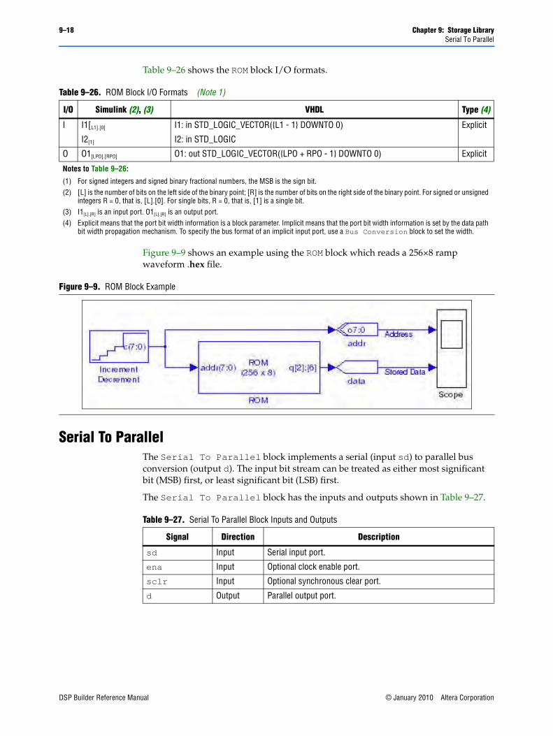
9–18 Chapter 9: Storage LibrarySerial To Parallel
Table 9–26 shows the ROM block I/O formats.
Figure 9–9 shows an example using the ROM block which reads a 256×8 ramp waveform .hex file.
Serial To ParallelThe Serial To Parallel block implements a serial (input sd) to parallel bus conversion (output d). The input bit stream can be treated as either most significant bit (MSB) first, or least significant bit (LSB) first.
The Serial To Parallel block has the inputs and outputs shown in Table 9–27.
Table 9–26. ROM Block I/O Formats (Note 1)
I/O Simulink (2), (3) VHDL Type (4)
I I1[L1].[0]
I2[1]
I1: in STD_LOGIC_VECTOR({L1 - 1} DOWNTO 0)
I2: in STD_LOGIC
Explicit
O O1[LPO].[RPO] O1: out STD_LOGIC_VECTOR({LPO + RPO - 1} DOWNTO 0) Explicit
Notes to Table 9–26:
(1) For signed integers and signed binary fractional numbers, the MSB is the sign bit.(2) [L] is the number of bits on the left side of the binary point; [R] is the number of bits on the right side of the binary point. For signed or unsigned
integers R = 0, that is, [L].[0]. For single bits, R = 0, that is, [1] is a single bit.(3) I1[L].[R] is an input port. O1[L].[R] is an output port.(4) Explicit means that the port bit width information is a block parameter. Implicit means that the port bit width information is set by the data path
bit width propagation mechanism. To specify the bus format of an implicit input port, use a Bus Conversion block to set the width.
Figure 9–9. ROM Block Example
Table 9–27. Serial To Parallel Block Inputs and Outputs
Signal Direction Description
sd Input Serial input port.
ena Input Optional clock enable port.
sclr Input Optional synchronous clear port.
d Output Parallel output port.
DSP Builder Reference Manual © January 2010 Altera Corporation

Chapter 9: Storage Library 9–19Serial To Parallel
Table 9–28 shows the Serial To Parallel block parameters.
Table 9–29 shows the Serial To Parallel block I/O formats.
Figure 9–10 shows an example using the Serial To Parallel block.
Table 9–28. Serial To Parallel Block Parameters
Name Value Description
Data Bus Type Signed Integer, Signed Fractional, Unsigned Integer
Choose the bus type format.
[number of bits].[] >= 0 (Parameterizable)
Specify the number of bits stored on the left side of the binary point including the sign bit.
[].[number of bits] >= 0 (Parameterizable)
Specify the number of bits stored on the right side of the binary point. This option applies only to signed fractional formats.
Serial Bit Order MSB First, LSB First Choose whether the MSB or LSB should be transmitted first.
Use Enable Port On or Off Turn on to use the clock enable input.
Use Synchronous Clear Port
On or Off Turn on to use the synchronous clear port (sclr).
Table 9–29. Serial To Parallel Block I/O Formats (Note 1)
I/O Simulink (2), (3) VHDL Type (4)
I I1[1]
I2[1]
I3[1]
I1: in STD_LOGIC
I2: in STD_LOGIC
I3: in STD_LOGIC
Explicit
O O1[L1].[R1] O1: in STD_LOGIC_VECTOR({L1 + R1 - 1} DOWNTO 0) Explicit
Notes to Table 9–29:
(1) For signed integers and signed binary fractional numbers, the MSB is the sign bit.(2) [L] is the number of bits on the left side of the binary point; [R] is the number of bits on the right side of the binary point. For signed or unsigned
integers R = 0, that is, [L].[0]. For single bits, R = 0, that is, [1] is a single bit.(3) I1[L].[R] is an input port. O1[L].[R] is an output port.(4) Explicit means that the port bit width information is a block parameter. Implicit means that the port bit width information is set by the data path
bit width propagation mechanism. To specify the bus format of an implicit input port, use a Bus Conversion block to set the width.
Figure 9–10. Serial To Parallel Block Example
© January 2010 Altera Corporation DSP Builder Reference Manual

9–20 Chapter 9: Storage LibraryShift Taps
Shift TapsThe Shift Taps block implements a shift register that you can use for filters or convolution.
In Stratix IV, Stratix III, Stratix II, Stratix II GX, Stratix GX, Arria GX, Arria II GX, Cyclone III, Cyclone II, and Cyclone devices, the block implements a RAM-based shift register that is useful for creating very large shift registers efficiently. The block outputs occur at regularly spaced points along the shift register (that is, taps).
In Stratix devices, this block is implemented in the small memory.
The Shift Taps block has the inputs and outputs shown in Table 9–30.
Table 9–31 shows the Shift Taps block parameters.
Table 9–32 shows the Shift Taps block I/O formats.
Table 9–30. Shift Taps Block Inputs and Outputs
Signal Direction Description
d Input Data input port.
ena Input Optional clock enable port.
t0–tn Output Output ports for taps 0–n.
sout Output Optional shift out port.
Table 9–31. Shift Taps Block Parameters
Name Value Description
Number of Taps User Defined (Parameterizable)
Specifies the number of regularly spaced taps along the shift register.
Distance Between Taps
User Defined (Parameterizable)
Specifies the distance between the regularly spaced taps in clock cycles. This translates to the number of RAM words that will be used.
Use Shift Out Port On or Off Turn on to create an output from the end of the shift register for cascading.
Use Enable port On or Off Turn on to use an additional clock enable control input.
Use Dedicated Circuitry
On or Off Turn on to enable selection of the memory block type. This option is only valid when the Distance Between Taps is greater than 2.
Memory Block Type
AUTO, M512, M4K, M9K, MLAB, M144K
Choose the RAM block type. Some memory types are not available for all device types.
Table 9–32. Shift Taps Block I/O Formats (Part 1 of 2) (Note 1)
I/O Simulink (2), (3) VHDL Type (4)
I I1[L1].[R1]
I2[1]
I1: in STD_LOGIC_VECTOR({L1 + R1 - 1} DOWNTO 0)
I2: in STD_LOGIC
Implicit
Explicit
DSP Builder Reference Manual © January 2010 Altera Corporation

Chapter 9: Storage Library 9–21Single-Port RAM
Figure 9–11 shows an example using the Shift Taps block.
Single-Port RAMThe Single-Port RAM block maps data to an embedded RAM (embedded array block, EAB; or embedded system block, ESB) in Altera devices. A single read/write port allow simple access.
The Single-Port RAM block accepts any type as data input. The input port is registered, and the output port can optionally be registered. The input address bus must be Unsigned. The clock enable signal (ena) bypasses any output register.
The contents of the RAM are pre-initialized to zero by default but can be specified using an Intel Hexadecimal (.hex) file or from a MATLAB array.
O O1[L1].[R1]
….
Oi[L1].[R1]
…
On[L1].[R1]
On+1[1]
O1: in STD_LOGIC_VECTOR({L1 + R1 - 1} DOWNTO 0)
….
Oi: in STD_LOGIC_VECTOR({L1 + R1 - 1} DOWNTO 0)
….
On: in STD_LOGIC_VECTOR({L1 + R1 - 1} DOWNTO 0)
On+1: out STD_LOGIC
Implicit
Explicit
Notes to Table 9–32:
(1) For signed integers and signed binary fractional numbers, the MSB is the sign bit.(2) [L] is the number of bits on the left side of the binary point; [R] is the number of bits on the right side of the binary point. For signed or unsigned
integers R = 0, that is, [L].[0]. For single bits, R = 0, that is, [1] is a single bit.(3) I1[L].[R] is an input port. O1[L].[R] is an output port.(4) Explicit means that the port bit width information is a block parameter. Implicit means that the port bit width information is set by the data path
bit width propagation mechanism. To specify the bus format of an implicit input port, use a Bus Conversion block to set the width.
Table 9–32. Shift Taps Block I/O Formats (Part 2 of 2) (Note 1)
I/O Simulink (2), (3) VHDL Type (4)
Figure 9–11. Shift Taps Block Example
© January 2010 Altera Corporation DSP Builder Reference Manual

9–22 Chapter 9: Storage LibrarySingle-Port RAM
You can use the Quartus II software to generate a .hex File which must be in your DSP Builder working directory.
The data in a standard .hex file is formatted in multiples of eight and the output bit width should also be in multiples of eight. The Quartus II software does allow you to create non-standard .hex files but pads 1's to the front for negative numbers to make them multiples of eight. Thus, large numbers with less bits may be treated as negative numbers. A warning is issued if you specify a non-standard .hex file. If you require a different bit width, you should set the output bit width to the same as that in the .hex file but use an AltBus block to convert to the required bit width. 32-bit addressing is supported using extended linear address records in the .hex file.
f For instructions on creating this file, refer to Creating a Memory Initialization File or Hexadecimal (Intel-Format) File in the Quartus II Help.
If used, the MATLAB array parameter must be a one dimensional MATLAB array with a length less than or equal to the number of words. The array can be specified from the MATLAB work-space or directly in the MATLAB Array box.
The Single-Port RAM block has the inputs and outputs shown in Table 9–33.
Table 9–34 shows the Single-Port RAM block parameters.
Table 9–33. Single-Port RAM Block Inputs and Outputs
Signal Direction Description
d Input Input data port.
addr Input Address bus.
wren Input Write enable.
ena Input Optional clock enable port
q_a Output Output data port.
Table 9–34. Single-Port RAM Block Parameters (Part 1 of 2)
Name Value Description
Number of words >= 1 (Parameterizable)
Specify the address width in words.
Data Type Inferred, Signed Integer, Unsigned Integer, Signed Fractional
Choose the input data type format.
[number of bits].[] >= 0 (Parameterizable)
Specify the number of bits stored on the left side of the binary point.
[].[number of bits] >= 0 (Parameterizable)
Specify the number of bits to the right of the binary point. This option applies only to signed fractional formats.
Memory Block Type
AUTO, M512, M4K, M-RAM, M9K, MLAB, M144K
Choose the FPGA RAM memory block type. Some memory types are not available for all device types. If you choose M-RAM, the RAM is always initialized to unknown in the hardware and simultaneous read/writes to the same address also give unknown in hardware. Note that unknowns are not modeled in Simulink, and comparisons with ModelSim will show differences.
Initialization Blank, From HEX file, From MATLAB array
Specify the initialization. If Blank is selected, the contents of the RAM are pre-initialized to zero.
DSP Builder Reference Manual © January 2010 Altera Corporation

Chapter 9: Storage Library 9–23Single-Port RAM
Table 9–35 shows the Single-Port RAM block I/O formats.
Input HEX File User defined Specify the name of a .hex file which must be in your DSP Builder working directory. For example: input.hex.
32-bit addressing is supported using extended linear address records in the .hex file.
MATLAB Array User defined (Parameterizable)
Specify a one-dimensional MATLAB array with a length less than or equal to the number of words. For example: [0:1:15]
Register output Port
On or Off Turn on to register the output port.
Use Enable Port On or Off Turn on to use the optional clock enable input (ena).
Clock Phase Selection
User Defined Specify the phase selection with a binary string, where a 1 indicates the phase in which the block is enabled. For example:
1—The block is always enabled and captures all data passing through the block (sampled at the rate 1).
10—The block is enabled every other phase and every other data (sampled at the rate 1) passes through.
0100—The block is enabled on the second phase of and only the second data of (sampled at the rate 1) passes through. That is, the data on phases 1, 3, and 4 do not pass through the delay block.
Table 9–34. Single-Port RAM Block Parameters (Part 2 of 2)
Name Value Description
Table 9–35. Single-Port RAM Block I/O Formats (Note 1)
I/O Simulink (2), (3) VHDL Type (4)
I I1[L1].[R1]
I2[L2].[0]
I3[1]
I4[1]
I1: in STD_LOGIC_VECTOR({L1 + R1 - 1} DOWNTO 0)
I2: in STD_LOGIC_VECTOR({L2 - 1} DOWNTO 0)
I3: in STD_LOGIC
I4: in STD_LOGIC
Explicit
O O1[L1].[R1] O1: out STD_LOGIC_VECTOR({L1 + R1 - 1} DOWNTO 0) Explicit
Notes to Table 9–12:
(1) For signed integers and signed binary fractional numbers, the MSB is the sign bit.(2) [L] is the number of bits on the left side of the binary point; [R] is the number of bits on the right side of the binary point. For signed or unsigned
integers R = 0, that is, [L].[0]. For single bits, R = 0, that is, [1] is a single bit.(3) I1[L].[R] is an input port. O1[L].[R] is an output port.(4) Explicit means that the port bit width information is a block parameter. Implicit means that the port bit width information is set by the data path
bit width propagation mechanism. To specify the bus format of an implicit input port, use a Bus Conversion block to set the width.
© January 2010 Altera Corporation DSP Builder Reference Manual

9–24 Chapter 9: Storage LibraryTrue Dual-Port RAM
Figure 9–12 shows an example using the Single-Port RAM block.
True Dual-Port RAMThe True Dual-Port RAM block maps data to an embedded RAM (embedded array block, EAB; or embedded system block, ESB) in Altera devices. Two read and two write ports allow true dual access.
The True Dual-Port RAM block accepts any data type as input. The input port is always registered and the output port can optionally be registered.
Turning on the DONT_CARE option may give a higher fMAX for your design, especially if the memory is implemented as a MLAB. When this option is on, the output is not double-registered (and therefore, in the case of MLAB implementation, uses fewer external registers), and you gain an extra half-cycle on the output. The default is off, which outputs old data for read-during-write.
f For more information about this option, refer to the Read-During-Write Output Behavior section in the RAM Megafunction User Guide.
The contents of the RAM are pre-initialized to zero by default but can be specified using an Intel Hexadecimal (.hex) file or from a MATLAB array. You can use the Quartus II software to generate a .hex File which must be in your DSP Builder working directory.
The data in a standard .hex file is formatted in multiples of eight and the output bit width should also be in multiples of eight. The Quartus II software does allow you to create non-standard .hex files but pads 1's to the front for negative numbers to make them multiples of eight. Thus, large numbers with less bits may be treated as negative numbers. A warning is issued if you specify a non-standard .hex file. If you require a different bit width, you should set the output bit width to the same as that in the .hex file but use an AltBus block to convert to the required bit width. 32-bit addressing is supported using extended linear address records in the .hex file.
f For instructions on creating this file, refer to Creating a Memory Initialization File or Hexadecimal (Intel-Format) File in the Quartus II Help.
If used, the MATLAB array parameter must be a one dimensional MATLAB array with a length less than or equal to the number of words. The array can be specified from the MATLAB workspace or directly in the MATLAB Array box.
Figure 9–12. Single-Port RAM Block Example
DSP Builder Reference Manual © January 2010 Altera Corporation

Chapter 9: Storage Library 9–25True Dual-Port RAM
The input address bus must be Unsigned. The clock enable signal (ena) bypasses any output register.
c If you write to the same address simultaneously with the a and b inputs, the data written to the RAM is indeterminate (corrupt). In ModelSim simulations, the data at this address is set to Unknown (all bits X). In DSP Builder simulation, the data at this address is set to zero, and a warning is given:
"Warning: True Dual-Port RAM: simultaneous a and b side writing to address <addr>. Memory contents at this address will be Unknown (X) in hardware."
If this data is read, DSP Builder warns that you are reading corrupt data:
"Warning: True Dual-Port RAM: <a|b>-side reading corrupt RAM data at address <addr>. Memory contents at this address will be Unknown (X) in hardware."
If you execute a testbench comparison to hardware, you may get simulation mismatches if you are making use of corrupt data in your design or outputting the read memory contents to a pin.
The True Dual-Port RAM block has the inputs and outputs shown in Table 9–36.
Table 9–37 shows the True Dual-Port RAM block parameters.
Table 9–36. True Dual-Port RAM Block Inputs and Outputs
Signal Direction Description
data_a Input Input data port a
addr_a Input Address bus a.
wren_a Input Write enable a
data_b Input Input data port b
addr_b Input Address bus b
wren_b Input Write enable b
ena Input Optional clock enable port
q_a Output Output data port a
q_b Output Output data port b
Table 9–37. True Dual-Port RAM Block Parameters (Part 1 of 2)
Name Value Description
Number of words >= 1 (Parameterizable)
Specify the address width in words.
Data Type Inferred, Signed Integer, Unsigned Integer, Signed Fractional
Choose the input data type format.
[number of bits].[] >= 0 (Parameterizable)
Specify the number of bits stored on the left side of the binary point.
[].[number of bits] >= 0 (Parameterizable)
Specify the number of bits to the right of the binary point. This option applies only to signed fractional formats.
© January 2010 Altera Corporation DSP Builder Reference Manual

9–26 Chapter 9: Storage LibraryTrue Dual-Port RAM
Memory Block Type AUTO, M512, M4K, M-RAM, M9K, MLAB, M144K
Choose the FPGA RAM memory block type. Some memory types are not available for all device types. If you choose M-RAM, the RAM is always initialized to unknown in the hardware and simultaneous read/writes to the same address give unknown in hardware. Note that unknowns are not modeled in Simulink, and comparisons with ModelSim will show differences.
Use DONT_CARE when reading from and writing to the same address
On or Off If the memory block type is set to AUTO, setting DONT_CARE gives more flexibility in RAM block placement. If the implementation is set to MLAB, fewer external registers are used, because the output is not double registered, and the resulting memory block can often be run at a higher fMax. However, the output in hardware when reading from and writing to the same address is unpredictable. In ModelSim simulation, unknowns (X) are output when reading from and writing to the same address. The Simulink simulation is unchanged whether or not you use this option, but a warning message is issued on every simultaneous read/write to the same address. If you compare the simulation results to ModelSim, you will see mismatches associated with any read/write to the same address events. When this option is set, ensure that the same address is not read from and written to at the same time or that your design does not depend on the read output in these circumstances. By default this option is off, and data is always read before write.
Initialization Blank, From HEX file, From MATLAB array
Specify the initialization. If Blank is selected, the contents of the RAM are pre-initialized to zero.
Input HEX File User defined Specify the name of an .hex file which must be in your DSP Builder working directory. For example: input.hex.
32-bit addressing is supported using extended linear address records in the .hex file.
MATLAB Array User defined (Parameterizable)
Specify a one-dimensional MATLAB array with a length less than or equal to the number of words. For example: [0:1:15]
Register output Ports On or Off Turn on to register the output ports.
Use Enable Port On or Off Turn on to use the optional clock enable input (ena).
Clock Phase Selection User Defined Specify the phase selection with a binary string, where a 1 indicates the phase in which the block is enabled. For example:
1—The block is always enabled and captures all data passing through the block (sampled at the rate 1).
10—The block is enabled every other phase and every other data (sampled at the rate 1) passes through.
0100—The block is enabled on the second phase of and only the second data of (sampled at the rate 1) passes through. That is, the data on phases 1, 3, and 4 do not pass through the block.
Table 9–37. True Dual-Port RAM Block Parameters (Part 2 of 2)
Name Value Description
DSP Builder Reference Manual © January 2010 Altera Corporation

Chapter 9: Storage Library 9–27True Dual-Port RAM
Table 9–38 shows the True Dual-Port RAM block I/O formats.
Figure 9–13 shows an example using the True Dual-Port RAM block.
Table 9–38. True Dual-Port RAM Block I/O Formats (Note 1)
I/O Simulink (2), (3) VHDL Type (4)
I I1[L1].[R1]
I2[L2].[0]
I3[L2].[0]
I4[L1].[R1]
I5[L2].[0]
I6[L2].[0]
I7[1]
I8[1]
I1: in STD_LOGIC_VECTOR({L1 + R1 - 1} DOWNTO 0)
I2: in STD_LOGIC_VECTOR({L2 - 1} DOWNTO 0)
I3: in STD_LOGIC_VECTOR({L3 - 1} DOWNTO 0)
I4: in STD_LOGIC_VECTOR({L4 + R4 - 1} DOWNTO 0)
I5: in STD_LOGIC_VECTOR({L5 - 1} DOWNTO 0)
I6: in STD_LOGIC_VECTOR({L6 - 1} DOWNTO 0)
I7: in STD_LOGIC
I8: in STD_LOGIC
Explicit
O O1[L1].[R1] O1: out STD_LOGIC_VECTOR({L1 + R1 - 1} DOWNTO 0) Explicit
Notes to Table 9–12:
(1) For signed integers and signed binary fractional numbers, the MSB is the sign bit.(2) [L] is the number of bits on the left side of the binary point; [R] is the number of bits on the right side of the binary point. For signed or unsigned
integers R = 0, that is, [L].[0]. For single bits, R = 0, that is, [1] is a single bit.(3) I1[L].[R] is an input port. O1[L].[R] is an output port.(4) Explicit means that the port bit width information is a block parameter. Implicit means that the port bit width information is set by the data path
bit width propagation mechanism. To specify the bus format of an implicit input port, use a Bus Conversion block to set the width.
Figure 9–13. True Dual-Port RAM Block Example
© January 2010 Altera Corporation DSP Builder Reference Manual

9–28 Chapter 9: Storage LibraryUp Sampling
Up SamplingThe Up Sampling block increases the output sample rate from the input sample rate. The output data is sampled every N cycles where N is equal to the up sampling rate. The output holds this value for 1 cycle, then for the next N-1 cycles the output is zero.
The Up Sampling block has the inputs and outputs shown in Table 9–39.
Table 9–40 shows the Up Sampling block parameter.
Table 9–41 shows the Up Sampling block I/O formats.
Figure 9–14 shows an example using the Up Sampling block.
Table 9–39. Up Sampling Block Inputs and Outputs
Signal Direction Description
d Input Input data port.
q Output Output data port.
Table 9–40. Up Sampling Block Parameter
Name Value Description
Up Sampling Rate An integer greater than 1 (Parameterizable)
Specify the up sampling rate.
Table 9–41. Up Sampling Block I/O Formats (Note 1)
I/O Simulink (2), (3) VHDL Type (4)
I I1[L1].[R1] I1: in STD_LOGIC_VECTOR({L1 + R1 - 1} DOWNTO 0) Implicit
O O1[L1].[R1] O1: in STD_LOGIC_VECTOR({L1 + R1 - 1} DOWNTO 0) Implicit
Notes to Table 9–41:
(1) For signed integers and signed binary fractional numbers, the MSB is the sign bit.(2) [L] is the number of bits on the left side of the binary point; [R] is the number of bits on the right side of the binary point. For signed or unsigned
integers R = 0, that is, [L].[0]. For single bits, R = 0, that is, [1] is a single bit.(3) I1[L].[R] is an input port. O1[L].[R] is an output port.(4) Explicit means that the port bit width information is a block parameter. Implicit means that the port bit width information is set by the data path
bit width propagation mechanism. To specify the bus format of an implicit input port, use a Bus Conversion block to set the width.
Figure 9–14. Up Sampling Block Example
DSP Builder Reference Manual © January 2010 Altera Corporation

© January 2010 Altera Corporation
10. State Machine Functions Library
The State Machine Functions library contains the following blocks:
■ State Machine Editor
■ State Machine Table
State Machine EditorThe State Machine Editor block provides access to the Quartus® II state machine editor which allows you to create graphic representations of state machines for use in your design.
A state machine is a very efficient means to specify complex control logic which can then be used to generate a HDL description and Simulink interface to the simulation model.
You can define a state machine graphically by adding states and transitions directly on the diagram, or by using a wizard interface to enter all the properties for the state machine. When you use the wizard interface, a graphical state diagram view is created with the states and transitions automatically placed for optimum readability.
Figure 10–1 shows the state machine that is created when you use the default options in the wizard.
Table 10–1 shows the parameters that can be set in the State Machine wizard.
Figure 10–1. Default State Machine Diagram View
Table 10–1. State Machine Wizard Parameters
Name Value Description
Which reset mode do you want to use
Synchronous, Asynchronous
Specifies whether the state machine has a synchronous or asynchronous reset.
Reset is active-high On, Off Turn on to uses an active-high reset or off if you want an active-low reset.
Register the output ports
On, Off Turn on to register the state machine output ports.
DSP Builder Reference Manual
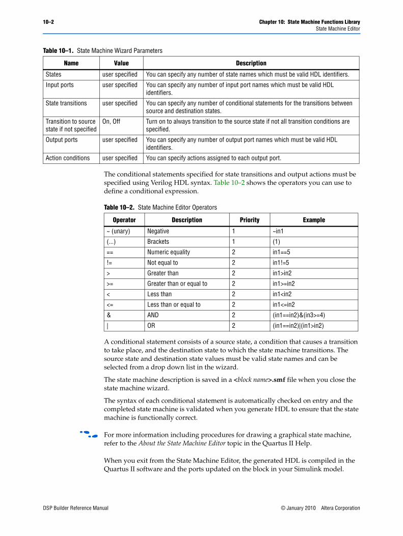
10–2 Chapter 10: State Machine Functions LibraryState Machine Editor
The conditional statements specified for state transitions and output actions must be specified using Verilog HDL syntax. Table 10–2 shows the operators you can use to define a conditional expression.
A conditional statement consists of a source state, a condition that causes a transition to take place, and the destination state to which the state machine transitions. The source state and destination state values must be valid state names and can be selected from a drop down list in the wizard.
The state machine description is saved in a <block name>.smf file when you close the state machine wizard.
The syntax of each conditional statement is automatically checked on entry and the completed state machine is validated when you generate HDL to ensure that the state machine is functionally correct.
f For more information including procedures for drawing a graphical state machine, refer to the About the State Machine Editor topic in the Quartus II Help.
When you exit from the State Machine Editor, the generated HDL is compiled in the Quartus II software and the ports updated on the block in your Simulink model.
States user specified You can specify any number of state names which must be valid HDL identifiers.
Input ports user specified You can specify any number of input port names which must be valid HDL identifiers.
State transitions user specified You can specify any number of conditional statements for the transitions between source and destination states.
Transition to source state if not specified
On, Off Turn on to always transition to the source state if not all transition conditions are specified.
Output ports user specified You can specify any number of output port names which must be valid HDL identifiers.
Action conditions user specified You can specify actions assigned to each output port.
Table 10–1. State Machine Wizard Parameters
Name Value Description
Table 10–2. State Machine Editor Operators
Operator Description Priority Example
~ (unary) Negative 1 ~in1
(...) Brackets 1 (1)
== Numeric equality 2 in1==5
!= Not equal to 2 in1!=5
> Greater than 2 in1>in2
>= Greater than or equal to 2 in1>=in2
< Less than 2 in1<in2
<= Less than or equal to 2 in1<=in2
& AND 2 (in1==in2)&(in3>=4)
| OR 2 (in1==in2)|(in1>in2)
DSP Builder Reference Manual © January 2010 Altera Corporation

Chapter 10: State Machine Functions Library 10–3State Machine Table
Figure 10–2 shows an example of the default state machine created by the State Machine Editor wizard included in a simple Simulink model.
f for a walkthrough example Using the State Machine Editor Block, refer to the DSP Builder User Guide.
State Machine TableThe State Machine Table block represents a one-hot Moore-style state machine where the output is equal to the current state (Figure 10–3).
The default state machine has five inputs and five states. Each state is represented by an output.
While the state machine is operating, an output is assigned a logic level 1 if its respective state is equal to the current state. All other outputs are assigned a logic level 0. The inputs and outputs are represented as integers in Simulink. In VHDL, the input and output are represented as standard logic vectors.
1 The State Machine Table block is not available on Linux and is deprecated on Windows. Use the State Machine Editor block in new designs.
Figure 10–2. Example Using the State Machine Editor Block
Figure 10–3. Moore Style State Machine
© January 2010 Altera Corporation DSP Builder Reference Manual

10–4 Chapter 10: State Machine Functions LibraryState Machine Table
The default State Machine Table symbol is shown in Figure 10–4.
The State Machine Builder dialog box allows you to specify the inputs, states, and conditional statements which control the transitions between the states.
Table 10–3 shows the controls available in the State Machine Builder dialog box.
Table 10–4 shows the operators that you can use to define a conditional expression.
Figure 10–4. Default State Machine Table Block
Table 10–3. State Transition Table Block Controls
Name Value Description
Add — Adds the specified input name, state name or conditional statement to the table.
Change — Allows you to change the selected state name or conditional statement. This option cannot be used in the Inputs tab. You cannot change an input name or state name that is being used in a conditional statement.
Delete — Deletes the selected input name, state name or conditional statement. You cannot delete an input or state that is being used in a conditional statement.
Reset State state name This option is available in the States tab and allows you to choose the reset state from a list of specified state names. You can change the reset state but you cannot delete or change the name of the reset state.
Move Up
Move Down
— These buttons are available in the Conditional Statements tab and allow you to change the transition priority when there is more than one condition leaving a state by moving the conditional statement up or down the list.
Analyze — This button is available in the Design Rule Check tab to validate your state machine table.
Table 10–4. State Machine Table Operators
Operator Description Priority Example
- (unary) Negative 1 -1
(...) Brackets 1 (1)
= Numeric equality 2 in1=5
!= Not equal to 2 in1!=5
> Greater than 2 in1>in2
>= Greater than or equal to 2 in1>=in2
< Less than 2 in1<in2
<= Less than or equal to 2 in1<=in2
& AND 2 (in1=in2)&(in3>=4)
| OR 2 (in1=in2)|(in1>in2)
DSP Builder Reference Manual © January 2010 Altera Corporation

Chapter 10: State Machine Functions Library 10–5State Machine Table
A conditional statement consists of a current state, a condition that causes a transition to take place, and the next state to which the state machine transitions. The current state and next state values must be state names defined in the States tab and can be selected from drop down list in the dialog box.
1 To indicate in a conditional statement that a state machine always transitions from the current state to the next state, specify the conditional expression to be one.
Figure 10–5 shows the dialog box used to specify a simple state transition table using the default inputs and states.
1 When VHDL is generated, the expression strings for the port names are replaced by signals named <port name>_sig.
At least one transition must be specified for each state. Otherwise, the block does not generate legal VHDL.
You may experience problems when using very large input signals (greater than 225).
Design Rule ChecksThe Analyze button in the Design Rule Checks tab of the State Machine Builder dialog box performs the following checks:
■ At least two states must be defined
■ At least two conditional statements must be defined
■ All input port names must be unique
■ All state names must be unique
Figure 10–5. Simple State Transition Table
© January 2010 Altera Corporation DSP Builder Reference Manual

10–6 Chapter 10: State Machine Functions LibraryState Machine Table
■ A single reset state must exist
■ A reset input port must exist
■ All current state and next state values must be valid
■ All conditional statements must be syntactically correct
Figure 10–6 shows an example using the State Machine Table block as a FIFO controller.
f for a walkthrough example Using the State Machine Table Block, refer to the DSP Builder User Guide.
Figure 10–6. Example Using the State Machine Table Block
DSP Builder Reference Manual © January 2010 Altera Corporation

© January 2010 Altera Corporation
11. Boards Library
The Boards library supports DSP development platforms for the following prototyping boards:
■ Cyclone II DE2 Board
■ Cyclone II EP2C35 DSP Board
■ Cyclone II EP2C70 DSP Board
■ Cyclone III EP3C25 Starter Board
■ Cyclone III EP3C120 DSP Board
■ Stratix EP1S25 DSP Board
■ Stratix EP1S80 DSP Board
■ Stratix II EP2S60 DSP Board
■ Stratix II EP2S180 DSP Board
■ Stratix II EP2S90GX PCI Express Board
■ Stratix III EP3SL150 DSP Board
These development boards provide an economical solution for hardware and software verification that enables you to debug and verify both functionality and design timing.
When combined with DSP intellectual property (IP) from Alteraor from the Altera Megafunction Partners Program (AMPPSM), you can solve design problems that formerly required custom hardware and software solutions.
Board ConfigurationWhen targeting a development board, your design must contain the corresponding board configuration block at the top hierarchical level. The configuration block properties allow you to choose from a list of available pins to use for the clock and global reset connections. It also displays details of the hardware device used on the board.
The other blocks available for each board provide connections to the controls on each board such as LEDs, push buttons, switches, 7-segment displays, connectors, analog-to-digital converters (ADC), and digital-to-analog converters (DAC). By using these blocks, you do not need to make pin assignments to connect the board components.
PLL Output ClocksIn DSP Builder v7.0 or earlier, one or more PLLs were automatically included to provide output clocks which are listed in the top level VHDL, with the clock locations assigned to the selected pins from the board configuration block.
DSP Builder Reference Manual

11–2 Chapter 11: Boards LibraryCyclone II DE2 Board
From DSP Builder v7.1, PLLs are no longer added in your design because there may be conflicting PLLs in higher levels of your design hierarchy. However, you can manually add PLL blocks to your design and configure them to provide the required output clocks using the Quartus II Pinout Assignments block to assign pin locations to the PLL outputs.
ADC Control SignalsThe ADC control signals are not automatically assigned on the Cyclone II EP2C35 DSP Board or the Cyclone II EP2C70 DSP Board. For these boards, you must make manual assignments using Quartus II Pinout Assignments blocks.
Figure 11–1 shows how this can be done using VCC and GND blocks to set the signal levels for the Cyclone II EP2C35 DSP Board.
Cyclone II DE2 BoardThe Cyclone II DE2 development and education board provides a complete, ready-to-teach platform based on the Altera Cyclone II 2C35 device for use in courses on logic design and computer organization.
Table 11–1 lists the blocks available to support the Cyclone II DE2 board.
Figure 11–1. ADC Reset Pin Assignments
Figure 11–2. Cyclone II DE2 Board
Table 11–1. Cyclone II DE2 Board Blocks (Part 1 of 2)
Block Description
LED0–LED17 Controls eighteen red user-definable LEDs.
LEDG0–LEDG8 Controls nine green user-definable LEDs.
DSP Builder Reference Manual © January 2010 Altera Corporation

Chapter 11: Boards Library 11–3Cyclone II DE2 Board
f For detailed information about the Cyclone II DE2 board, refer to Altera’s Development and Education Board on the Altera website.
Figure 11–3 shows the example design for the Cyclone II DE2 board.
PB0–PB3 Controls four user-definable active-low push buttons. You can optionally specify the clock signal.
PROTO and PROTO1
Two Santa Cruz connectors which control the prototyping area I/O. You can optionally choose Input or Output node type, specify the input clock signal, and choose the pin location for each connector.
Display0-Display7 Control eight simple user-definable seven-segment LED displays.
SW0–SW17 Controls eighteen user-definable active-low toggle switches. You can optionally specify the clock signal.
Table 11–1. Cyclone II DE2 Board Blocks (Part 2 of 2)
Block Description
Figure 11–3. Example Design for the Cyclone II DE2 Board
© January 2010 Altera Corporation DSP Builder Reference Manual

11–4 Chapter 11: Boards LibraryCyclone II EP2C35 DSP Board
Cyclone II EP2C35 DSP BoardThe Cyclone II EP2C35 DSP board provides a low-cost hardware platform for developing high performance DSP designs based on Altera Cyclone II FPGA devices.
Table 11–2 lists the blocks available to support the Cyclone II EP2C35 DSP board.
f For information about setting up the board, refer to the DSP Development Kit, Cyclone II Getting Started User Guide. For information about supported hardware features, refer to the Cyclone II DSP Development Board Reference Manual.
Figure 11–4. Cyclone II EP2C35 DSP Board
Table 11–2. Cyclone II EP2C35 DSP Board Blocks
Block Description
A2D_1 Controls the 12-bit signed analog-to-digital converter (U26). You can optionally specify the clock signal.
D2A_1 Controls the 14-bit unsigned digital-to-analog converter (U25).
Dip Switch Controls the user-definable dual in-line package switch (S1). You can optionally specify the clock signal.
LED0–LED7 Controls eight user-definable LEDs (D2–D9).
PROTO and PROTO1
Santa Cruz connectors which control the prototyping area I/O. You can optionally choose Input or Output node type, specify the input clock signal, and choose the pin location for each connector (J15, J22, J23).
Display0 and Display1
Controls two simple user-definable seven-segment LED displays (U32, U33).
SW2–SW5, USER_RESETN
Controls four user-definable push-button switches (SW2–SW5, and user reset push-button SW6). You can optionally specify the clock signal.
DSP Builder Reference Manual © January 2010 Altera Corporation

Chapter 11: Boards Library 11–5Cyclone II EP2C70 DSP Board
Figure 11–5 shows the example design for the Cyclone II EP2C35 DSP board.
Cyclone II EP2C70 DSP BoardThe Cyclone II EP2C70 DSP board is an enhanced version of the EP2C35 board which has two 14-bit analog-to-digital converters and two 14-bit digital-to-analog converters.
Figure 11–5. Example Design for the Cyclone II EP2C35 DSP Board
Figure 11–6. Cyclone II EP2C70 DSP Board
© January 2010 Altera Corporation DSP Builder Reference Manual

11–6 Chapter 11: Boards LibraryCyclone II EP2C70 DSP Board
Table 11–3 lists the blocks available to support the Cyclone II EP2C70 DSP board.
f For information about setting up the board, refer to the DSP Development Kit, Cyclone II Getting Started User Guide. For information about supported hardware features, refer to the Cyclone II DSP Development Board Reference Manual.
Figure 11–7 shows the example design for the Cyclone II EP2C70 DSP board.
Table 11–3. Cyclone II EP2C70 DSP Board Blocks
Block Description
A2D_1 and A2D_2 Controls the 14-bit signed analog-to-digital converters. You can optionally specify the clock signal.
D2A_1 and D2A_2 Controls the 14-bit unsigned digital-to-analog converters.
Dip Switch Controls the user-definable dual in-line package switch (S1). You can optionally specify the clock signal.
LED0–LED7 Controls eight user-definable LEDs (D2–D9).
PROTO and PROTO1
Santa Cruz connectors which control the prototyping area I/O. You can optionally choose Input or Output node type, specify the input clock signal, and choose the pin location for each connector (J15, J22, J23).
Display0 and Display1
Controls two simple user-definable seven-segment LED displays (U32, U33).
SW2–SW5, USER_RESETN
Controls four user-definable push-button switches (SW2–SW5, and the user reset push-button SW6). You can optionally specify the clock signal.
Figure 11–7. Example Design for the Cyclone II EP2C70 DSP Board
DSP Builder Reference Manual © January 2010 Altera Corporation

Chapter 11: Boards Library 11–7Cyclone III EP3C25 Starter Board
Cyclone III EP3C25 Starter BoardThe Cyclone III EP3C25 starter board is a hardware platform that you can customize using optional expansion connectors and daughtercards to evaluate the feature rich, low-power Altera Cyclone III device.
Table 11–4 lists the blocks available to support the Cyclone III EP3C25 starter board.
f For information about setting up the board, refer to the Cyclone III FPGA Starter Kit User Guide. For information about supported hardware features, refer to the Cyclone III FPGA Starter Board Reference Manual.
Figure 11–9 shows the example design for the Cyclone III EP3C25 starter board.
Figure 11–8. Cyclone III EP3C25 Starter Board
Table 11–4. Cyclone III EP3C25 Starter Board Blocks
Block Description
LED1–LED4 Controls four user-definable LEDs.
SW1–SW4, USER_RESETN
Controls four user-definable push-button switches and the user reset push button. You can optionally specify the clock signal.
Figure 11–9. Example Design for the Cyclone III EP3C25 Starter Board
© January 2010 Altera Corporation DSP Builder Reference Manual

11–8 Chapter 11: Boards LibraryCyclone III EP3C120 DSP Board
Cyclone III EP3C120 DSP BoardThe Cyclone III EP3C120 DSP board provides a hardware platform for developing and prototyping low-power, high-volume, feature-rich designs that demonstrate the Cyclone III device’s on-chip memory, embedded multipliers, and the Nios® II embedded soft processor.
Table 11–5 lists the blocks available to support the Cyclone III EP3C120 DSP board.
f For information about setting up the board, and supported hardware features, refer to the Cyclone III Development Board, Reference Manual.
There are four example designs for the Cyclone III EP3C120 DSP board:
■ Test3C120Board_Leds.mdl: This design tests the LEDs and push-button switches on the main development board.
Figure 11–10. Cyclone III EP3C120 DSP Board
Table 11–5. Cyclone III EP3C120 DSP Board Blocks
Block Description
Display0 User defined 4-digit seven-segment LED display (U30).
A2D_1_HSMC_A, A2D_1_HSMC_B, A2D_2_HSMC_A,
A2D_2_HSMC_B
Controls 14-bit signed analog-to-digital converters on the optional high speed mezzanine cards (HSMC). You can optionally specify the clock signal.
D2A_1_HSMC_A, D2A_1_HSMC_B, D2A_2_HSMC_A, D2A_2_HSMC_B
Controls the 14-bit unsigned digital-to-analog converters on the optional high speed mezzanine cards (HSMC).
Dip Switch Controls the user-definable dual in-line package switch (SW6). You can optionally specify the clock signal.
LED0–LED7 Controls eight user-definable LEDs (D26–D33).
PB0–PB3, CPU_RESETN
Controls four user-definable push-button switches (S1–S4) and the CPU reset push-button (S5). You can optionally specify the clock signal.
DSP Builder Reference Manual © January 2010 Altera Corporation

Chapter 11: Boards Library 11–9Cyclone III EP3C120 DSP Board
■ Test3C120Board_QuadDisplay.mdl: This design tests the 7-segment display on the main development board.
■ Test3C120Board_HSMA.mdl: This design tests the analog-to-digital and digital-to-analog converters on the daughtercard connected to HSMC port A.
■ Test3C120Board_HSMB.mdl: This design tests the analog-to-digital and digital-to-analog converters on the daughtercard connected to HSMC port B.
Figure 11–11 shows the test design for the LEDs and push buttons.
Figure 11–12 shows the test design for the 7-segment display.
Figure 11–11. LED and Push-button Example Design for the Cyclone III EP3C120 DSP Board Blocks
Figure 11–12. 7-Segment Display Example Design for the Cyclone III EP3C120 DSP Board Blocks
© January 2010 Altera Corporation DSP Builder Reference Manual

11–10 Chapter 11: Boards LibraryCyclone III EP3C120 DSP Board
Figure 11–13 shows the test design for a high speed mezzanine card.
1 Figure 11–13 shows the test design for the daughtercard connected to HSMC port A. The test design for the daughtercard connected to HSMC port B is very similar.
Setting Up the Mezzanine Card Test DesignsThe required pin and clock assignments are already set up in the example designs. If necessary, you can set up your own test design as follows:
1. The following Quartus II Global project assignments must be set with the value “Use AS REGULAR I/O”:
■ RESERVE_DATA1_AFTER_CONFIGURATION
■ CYCLONEII_RESERVE_NCEO_AFTER_CONFIGURATION
■ RESERVE_DCLK_AFTER_CONFIGURATION
These assignments enable the programmer pins to be used as I/O.
2. Assign signals to the output enable pins for both channels of the analog-to-digital converters (A2D1_OEB and A2D2_OEB) and tie them to GND.
3. Assign signals to the SPI bus interface signals for the chip in static mode (ADA_SPI_CSB and ADA_SPI_CSB) and tie them to VCC. When these signal are pulled high, the following signals can be set:
AD_SCLK:
■ High: Two’s complement output (for FIR or similar)
■ Low: Straight binary from near midrange
AD_SDIO:
■ High: Duty cycle stabilizer (DCS) enabled to lower jitter
■ Low: DSC disabled
Figure 11–13. HSMC Example Design for the Cyclone III EP3C120 DSP Board Blocks
DSP Builder Reference Manual © January 2010 Altera Corporation

Chapter 11: Boards Library 11–11Cyclone III EP3C120 DSP Board
4. Open a Quartus II project and configure a PLL to produce the required output clocks:
a. Create a new block design file (for example, pll_clkout.bdf) and use the MegaWizard™ Plug-in Manager to add an ALTPLL megafunction.
b. Configure the PLL with a 50MHz input clock (inclk0) and no other optional inputs. (Turn off areset.) Turn on Create ‘locked’ output. Add two additional output clocks with 180 and 270 degrees phase shift from the input clock (c1 and c2) and clock multiplication factor of 2.
Figure 11–14 shows the completed block design file.
1 Each output clock is negated in the block editor to produce a the signals pclk0p, pclk0n, pclk1p, and pclk1n.
c. Choose Create HDL File for Current File from the File menu.
5. Import the PLL into the test design model:
a. Add a Subsystem Builder block to your model. Double-click on the block and browse for the HDL file created in step 4c then click Build to create the subsystem.
b. Open the subsystem (pll_clkout) and remove the default input port. Specify the clock name (such as clkin_50) in the block parameters for the HDL Entity block. This name should match the clock name used in the .bdf file.
c. Assign appropriate pin assignments for the four output clocks on the test design model (Figure 11–15.)
Figure 11–14. Configured PLL in the Quartus II Block Design Editor
Figure 11–15. PLL Subsystem
© January 2010 Altera Corporation DSP Builder Reference Manual

11–12 Chapter 11: Boards LibraryStratix EP1S25 DSP Board
Stratix EP1S25 DSP BoardThe Stratix EP1S25 DSP board is a powerful development platform for digital signal processing (DSP) designs, and features the Stratix EP1S25 device in the speed grade (-5) 780-pin package.
Table 11–6 lists the blocks available to support the Stratix EP1S25 DSP board.
Figure 11–16. Stratix EP1S25 DSP Board
Table 11–6. Stratix EP1S25 DSP Board Blocks
Block Description
A2D_1 and A2D_2 Controls the 12-bit signed analog-to-digital converters (U10, U30). You can optionally specify the clock signal.
D2A_1 and D2A_2 Controls the 14-bit unsigned digital-to-analog converters (U21, U23)
DEBUGA and DEBUGB
Mictor connectors which control debugging ports A and B. You can optionally choose Input or Output node type, specify the input clock signal, and choose the pin location for each port (J9, J10).
Dip Switch Controls the user-definable dual in-line package switch (SW3). You can optionally specify the clock signal.
EVAL IO IN and EVAL IO OUT
Controls the evaluation inputs and outputs. You can optionally specify the input clock signal for EVAL IO IN and choose the pin location for each input or output (JP7, JP19, JP22, JP20, JP21, JP24, JP8).
LED0 and LED1 Controls two user-definable LEDs (D6, D7).
PROTO Expansion connector which controls the prototyping area I/O. You can optionally choose Input or Output node type, specify the input clock signal, and choose the pin locations (J20, J21, J24).
RS232 ROUT and RS232 TIN
Controls the RS232 serial receive output and transmit input (J8). You can optionally specify the clock signal for RS232 TIN.
Display0 and Display1
Controls a dual user-definable seven-segment LED display (D4).
SW0–SW2 Controls three user-definable push-button switches (SW0–SW2). You can optionally specify the clock signal.
DSP Builder Reference Manual © January 2010 Altera Corporation

Chapter 11: Boards Library 11–13Stratix EP1S25 DSP Board
f For information about setting up the board, refer to the DSP Development Kit, Stratix & Stratix Professional Edition Getting Started User Guide. For information about the supported hardware features, refer to the Stratix EP1S25 DSP Development Board Data Sheet.
Figure 11–17 shows the example design for the Stratix EP1S25 DSP board.
Figure 11–17. Example Design for the Stratix EP1S25 DSP Board
© January 2010 Altera Corporation DSP Builder Reference Manual

11–14 Chapter 11: Boards LibraryStratix EP1S80 DSP Board
Stratix EP1S80 DSP BoardThe Stratix EP1S80 DSP board is a powerful development platform for digital signal processing (DSP) designs, and features the Stratix EP1S80 device in the speed grade (-6) 956-pin package.
Table 11–7 lists the blocks available to support the Stratix EP1S80 DSP board.
Figure 11–18. Stratix EP1S80 DSP Board
Table 11–7. Stratix EP1S80 DSP Board Blocks
Block Description
A2D_1 and A2D_2 Controls the 12-bit signed analog-to-digital converters (U10, U30). You can optionally specify the clock signal.
D2A_1 and D2A_2 Controls the 14-bit unsigned digital-to-analog converters (U21, U23)
DEBUGA and DEBUGB
Mictor connectors which control debugging ports A and B. You can optionally choose Input or Output node type, specify the input clock signal, and choose the pin location for each port (J9, J10).
Dip Switch Controls the user-definable dual in-line package switch (SW3). You can optionally specify the clock signal.
EVAL IO IN and EVAL IO OUT
Controls the evaluation input and outputs. You can optionally specify the clock signal for EVAL IO IN and choose the pin location for each input or output (JP7, JP19, JP22, JP20, JP21, JP24, JP8).
LED0 and LED1 Controls two user-definable LEDs (D6, D7).
PROTO Expansion connector which controls the prototyping area I/O. You can optionally choose Input or Output node type, specify the input clock signal, and choose the pin locations (J20, J21, J24).
RS232 ROUT and RS232 TIN
Controls the RS232 serial receive output and transmit input (J8). You can optionally specify the clock signal for RS232 TIN.
Display0 and Display1
Controls a dual user-definable seven-segment LED display (D4).
SW0–SW2 Controls three user-definable push-button switches (SW0–SW2). You can optionally specify the clock signal.
DSP Builder Reference Manual © January 2010 Altera Corporation

Chapter 11: Boards Library 11–15Stratix II EP2S60 DSP Board
f For information about setting up the board, refer to the DSP Development Kit, Stratix & Stratix Professional Edition Getting Started User Guide. For information about the supported hardware features, refer to the Stratix EP1S80 DSP Development Board Data Sheet.
Figure 11–19 shows the example design for the Stratix EP1S80 DSP board.
Stratix II EP2S60 DSP BoardThe Stratix II EP2S60 DSP board is a development platform for high-performance digital signal processing (DSP) designs, and features the Stratix II EP2S60 device in a 1020-pin package.
1 The Stratix II EP2S60 DSP board supports alternative EP2S60F1020C4 and EP2S60F1020C4ES devices which can be selected in the configuration block properties.
Figure 11–19. Example Design for the Stratix EP1S80 DSP Board
Figure 11–20. Stratix EP2S60 DSP Board
© January 2010 Altera Corporation DSP Builder Reference Manual

11–16 Chapter 11: Boards LibraryStratix II EP2S60 DSP Board
Table 11–8 lists the blocks available to support the Stratix EP2S60 DSP board.
f For information about setting up the board, refer to the DSP Development Kit Getting Started User Guide. For information about the supported hardware features, refer to the Stratix II DSP Development Board Reference Manual.
Figure 11–21 shows a test design using the SignalTap II and EP2S60 DSP board blocks. The 7-segment display and LEDs on the board respond to user-controlled switches and the value of the incrementer.
Table 11–8. Stratix EP2S60 DSP Board Blocks
Block Description
A2D_1 and A2D_2 Controls the 12-bit signed analog-to-digital converters (U1, U2). You can optionally specify the clock signal.
D2A_1 and D2A_2 Controls the 14-bit unsigned digital-to-analog converters (U14, U15)
IO_DEV_CLRn Controls the board reset push-button switch (SW8). You can optionally specify the clock signal.
LED0–LED7 Controls eight user-definable LEDs (D1–D8).
PROTO and PROTO1
Santa Cruz connectors which controls the prototyping area I/O. You can optionally choose Input or Output node type, specify the input clock signal, and choose the pin locations (J23– J25, J26–J28).
PROTO2 Mictor connector which controls the debugging port. You can optionally choose Input or Output node type, specify the input clock signal, and choose the pin location for each port (J20).
PROTO3 External analog-to-digital converter interface connector. You can optionally choose Input or Output node type, specify the input clock signal, and choose the pin location for each port (J5, J6).
Display0 and Display1
Controls a dual user-definable seven-segment LED display (U12, U13).
SW4–SW7 Controls four user-definable push-button switches (SW4–SW7). You can optionally specify the clock signal.
Figure 11–21. Example Design for the Stratix II EP2S60 DSP Board
DSP Builder Reference Manual © January 2010 Altera Corporation

Chapter 11: Boards Library 11–17Stratix II EP2S180 DSP Board
Stratix II EP2S180 DSP BoardThe Stratix II EP2S180 DSP board is a development platform for high-performance digital signal processing (DSP) designs, and features the Stratix II EP2S180 device in a 1020-pin package.
Table 11–9 lists the blocks available to support the Stratix EP2S180 DSP board.
f For information about setting up the board, refer to the DSP Development Kit Getting Started User Guide. For information about the supported hardware features, refer to the Stratix II EP2S180 DSP Development Board Reference Manual.
Figure 11–22. Stratix EP2S180 DSP Board
Table 11–9. Stratix EP2S180 DSP Board Blocks
Block Description
A2D_1 and A2D_2 Controls the 12-bit signed analog-to-digital converters (U1, U2). You can optionally specify the clock signal.
D2A_1 and D2A_2 Controls the 14-bit unsigned digital-to-analog converters (U14, U15)
IO_DEV_CLRn Controls the board reset push-button switch (SW8). You can optionally specify the clock signal.
LED0–LED7 Controls eight user-definable LEDs (D1–D8).
PROTO and PROTO1
Santa Cruz connectors which controls the prototyping area I/O. You can optionally choose Input or Output node type, specify the input clock signal, and choose the pin locations (J23– J25, J26–J28).
PROTO2 Mictor connector which controls the debugging port. You can optionally choose Input or Output node type, specify the input clock signal, and choose the pin location for each port (J20).
PROTO3 External analog-to-digital converter interface connector. You can optionally choose Input or Output node type, specify the input clock signal, and choose the pin location for each port (J5, J6).
Display0 and Display1
Controls a dual user-definable seven-segment LED display (U12, U13).
SW4–SW7 Controls four user-definable push-button switches (SW4–SW7). You can optionally specify the clock signal.
© January 2010 Altera Corporation DSP Builder Reference Manual

11–18 Chapter 11: Boards LibraryStratix II EP2S90GX PCI Express Board
Figure 11–23 shows the example design for the Stratix II EP2S180 DSP board. The 7-segment display and LEDs on the board respond to user-controlled switches and the value of the incrementer.
Stratix II EP2S90GX PCI Express BoardThe Stratix II EP2S90GX PCI Express board is a hardware platform for developing and prototyping high-performance PCI Express (PCIe)-based designs and also to demonstrate the Stratix II GX device’s embedded transceiver and memory circuitry.
Table 11–10 on page 11–19 lists the blocks available to support the Stratix II EP2S90GX PCI Express board.
Figure 11–23. Example Design for the Stratix II EP2S180 DSP Board
Figure 11–24. Stratix EP2S90GX PCI Express Board
DSP Builder Reference Manual © January 2010 Altera Corporation

Chapter 11: Boards Library 11–19Stratix II EP2S90GX PCI Express Board
f For information about setting up the board, refer to the PCI Express Development Kit, Stratix II GX Edition, Getting Started User Guide. For information about the supported hardware features, refer to the Stratix II GX PCI Express Development Board, Reference Manual.
Figure 11–25 shows the example design for the Stratix II EP2S90GX PCI Express board.
Table 11–10. Stratix EP2S90GX PCI Express Board Blocks
Block Description
Dip Switch Controls the user-definable dual in-line package switch (S5). You can optionally specify the clock signal.
LED0–LED7 Controls eight user-definable LEDs D9–D16).
SW2–SW4 Controls three user-definable push-button switches (S2–S4). You can optionally specify the clock signal.
Figure 11–25. Example Design for the Stratix II EP2S90GX PCI Express Board
© January 2010 Altera Corporation DSP Builder Reference Manual

11–20 Chapter 11: Boards LibraryStratix III EP3SL150 DSP Board
Stratix III EP3SL150 DSP BoardThe Stratix III EP3SL150 DSP board provides a hardware platform for developing and prototyping low-power, high-volume, feature-rich designs that demonstrate the Stratix III device’s on-chip memory, embedded multipliers, and the Nios® II embedded soft processor.
Table 11–11 lists the blocks available to support the Stratix III EP3SL150 DSP board.
f For information about setting up the board and the supported hardware features, refer to the Stratix III Development Board, Reference Manual.
There are four example designs for the Stratix III EP3SL150 DSP board:
■ Test3S150Board_Leds.mdl: This design tests the LEDs and push-button switches on the main development board.
■ Test3S150Board_QuadDisplay.mdl: This design tests the 7-segment display on the main development board.
Figure 11–26. Stratix III EP3SL150 DSP Board
Table 11–11. Stratix III EP3SL150 DSP Board Blocks
Block Description
Display0 User defined 4-digit seven-segment LED display (U27).
A2D_1_HSMC_A, A2D_1_HSMC_B, A2D_2_HSMC_A,
A2D_2_HSMC_B
Controls 14-bit signed analog-to-digital converters on the optional high speed mezzanine cards (HSMC). You can optionally specify the clock signal.
D2A_1_HSMC_A, D2A_1_HSMC_B, D2A_2_HSMC_A, D2A_2_HSMC_B
Controls the 14-bit unsigned digital-to-analog converters on the optional high speed mezzanine cards (HSMC).
Dip Switch Controls the user-definable dual in-line package switch (SW5). You can optionally specify the clock signal.
LED0–LED7 Controls eight user-definable LEDs (D20–D27).
PB0–PB3, CPU_RESETN
Controls four user-definable push-button switches (S2–S5) and the CPU reset push-button (S6). You can optionally specify the clock signal.
DSP Builder Reference Manual © January 2010 Altera Corporation

Chapter 11: Boards Library 11–21Stratix III EP3SL150 DSP Board
■ Test3S150Board_HSMA.mdl: This design tests the analog-to-digital and digital-to-analog converters on the daughtercard connected to HSMC port A.
■ Test3S150Board_HSMB.mdl: This design tests the analog-to-digital and digital-to-analog converters on the daughtercard connected to HSMC port B.
Figure 11–27 shows the test design for the LEDs and push-button switches.
Figure 11–28 shows the test design for the 7-segment display.
Figure 11–27. LED and Push-button Example Design for the Stratix III EP3SL150 DSP Board Blocks
Figure 11–28. 7-Segment Display Example Design for the Stratix III EP3SL150 DSP Board Blocks
© January 2010 Altera Corporation DSP Builder Reference Manual

11–22 Chapter 11: Boards LibraryStratix III EP3SL150 DSP Board
Figure 11–29 shows the test design for a high speed mezzanine card.
1 Figure 11–29 shows the test design for the daughtercard connected to HSMC port A. The test design for the daughtercard connected to HSMC port B is very similar.
Setting Up the Mezzanine Card Test DesignsThe required pin and clock assignments are already set up in the example designs. If necessary, you can set up your own test design by using similar procedures to those described for the Cyclone III EP3C120 DSP Board on page 11–10.
Figure 11–29. HSMC Example Design for the Stratix III EP3SL150 DSP Board Blocks
DSP Builder Reference Manual © January 2010 Altera Corporation

© January 2010 Altera Corporation
12. MegaCore Functions Library
The MegaCore Functions library contains blocks that represent parameterizable MegaCore® functions in the MegaCore IP library that is installed with the Quartus II software.
The following MegaCore functions are supported in DSP Builder:
■ CIC—Implements a cascaded integrator-comb) filter.
f For more information, refer to the CIC MegaCore Function User Guide.
■ FFT—Implements a high performance fast Fourier transform or inverse FFT processor.
f For more information, refer to the FFT MegaCore Function User Guide.
■ FIR Compiler—Implements a finite impulse response filter.
f For more information, refer to the FIR Compiler User Guide.
■ NCO—Implements a customized numerically controlled oscillator.
f For more information, refer to the NCO MegaCore Function User Guide.
■ Reed-Solomon Compiler—Implements a forward error correction encoder or decoder.
f For more information, refer to the Reed-Solomon Compiler User Guide.
■ Viterbi Compiler—Implements a high performance Viterbi decoder.
f For more information, refer to the Viterbi Compiler User Guide.
When you double-click on a MegaCore function block, the MegaWizard Plug-In Manager is invoked. The MegaWizard interface allows you to generate all the files required to integrate a parameterized MegaCore function variation into your DSP Builder model.
DSP Builder Reference Manual

12–2 Chapter 12: MegaCore Functions Library
DSP Builder Reference Manual © January 2010 Altera Corporation

Chapter 12: MegaCore Functions Library 12–3
© January 2010 Altera Corporation DSP Builder Reference Manual

12–4 Chapter 12: MegaCore Functions Library
DSP Builder Reference Manual © January 2010 Altera Corporation

Chapter 12: MegaCore Functions Library 12–5
© January 2010 Altera Corporation DSP Builder Reference Manual

12–6 Chapter 12: MegaCore Functions Library
DSP Builder Reference Manual © January 2010 Altera Corporation

© January 2010 Altera Corporation
A.Exam ple Designs
DSP Builder provides a variety of example designs, which you can use to learn from or as a starting point for your own design.
Tutorial Designs:
■ Amplitude Modulation
■ HIL Frequency Sweep
■ Switch Control
■ Avalon-MM Interface
■ Avalon-MM FIFO
■ HDL Import
■ Subsystem Builder
■ Custom Library
■ State Machine Table
Demonstration Designs:
■ CIC Interpolation (3 Stages x75)
■ CIC Decimation (3 Stages x75)
■ Convolution Interleaver Deinterleaver
■ IIR Filter
■ 32 Tap Serial FIR Filter
■ MAC based 32 Tap FIR Filter
■ Color Space Converter
■ Farrow Based Resampler
■ CORDIC, 20 bits Rotation Mode
■ Imaging Edge Detection
■ Quartus II Assignment Setting Example
■ SignalTap II Filtering Lab
■ SignalTap II Filtering Lab with DAC to ADC Loopback
■ Cyclone II DE2 Board
■ Cyclone II EP2C35 DSP Board
■ Cyclone II EP2C70 DSP Board
■ Cyclone III EP3C25 Starter Board
■ Cyclone III EP3C120 DSP Board (LED/PB)
■ Cyclone III EP3C120 DSP Board (7-Seg)
DSP Builder Reference Manual

A–2 Appendix A: Example Designs
■ Cyclone III EP3C120 DSP Board (HSMC A)
■ Cyclone III EP3C120 DSP Board (HSMC B)
■ Stratix EP1S25 DSP Board
■ Stratix EP1S80 DSP Board
■ Stratix II EP2S60 DSP Board
■ Stratix II EP2S180 DSP Board
■ Stratix II EP2S90GX PCI Express Board
■ Stratix III EP3SL150 DSP Board (LED/PB)
■ Stratix III EP3SL150 DSP Board (7-Seg)
■ Stratix III EP3SL150 DSP Board (HSMC A)
■ Stratix III EP3SL150 DSP Board (HSMC B)
The following additional example design demonstrates how you can combine blocks from the advanced and standard blocksets in a single design:
■ Combined Blockset Example
To view the example designs, type demo at the MATLAB command prompt. The Demos tab opens in the Help window displaying a list of example designs.
You can choose DSP Builder Blockset in the Help window to expand the list as shown in Figure A–1 and click on an entry to display an overview of each design.
Figure A–1. DSP Builder Design Example Demos
DSP Builder Reference Manual © January 2010 Altera Corporation

Appendix A: Example Designs A–3Amplitude Modulation
You can display the model corresponding to each example design by clicking Run this demo in the Help window. For example, if you click Run this demo for the Hardware in the Loop example, the model design window opens displaying the HIL frequency sweep model as shown in Figure A–2.
You can also click the or buttons to page forwards or backwards through the overview descriptions in the right hand pane of the Help window.
Tutorial DesignsThe <DSP Builder install path>\DesignExamples\Tutorials\ directory contains the example designs that are used in the Getting Started tutorial, walkthroughs, and other examples in the DSP Builder User Guide.
1 You can also access simple example models for most of the blocks in the DSP Builder blockset that correspond to the examples illustrated in the block descriptions. Many of these example blocks include Simulink Scope blocks which display the output waveforms when you simulate the models. These examples can be accessed in the directory <DSP Builder install path>\DesignExamples\Tutorials\UnitBlocks
Amplitude ModulationThe Getting Started tutorial uses an example amplitude modulation design to demonstrate the DSP Builder design flow. The design example is a modulator that has a sine wave generator, a quadrature multiplier, and a delay element.
The example model is named singen.mdl.
f For more information about this design, refer to the Getting Started Tutorial chapter in the DSP Builder User Guide.
Figure A–2. Hardware in the Loop Example Model
© January 2010 Altera Corporation DSP Builder Reference Manual

A–4 Appendix A: Example DesignsHIL Frequency Sweep
HIL Frequency SweepThis HIL (Hardware in the Loop) design is an example of a low-pass filter applied on the output of a modulated sine wave generation created using the CORDIC algorithm.
The example model is named FreqSweep_HIL.mdl.
f For more information about this design, refer to the HIL Walkthrough in the Using Hardware in the Loop (HIL) chapter of the DSP Builder User Guide.
Switch ControlThis example shows how you can use blocks to control the switches on a DSP Development board and how to perform the SignalTap II analysis in DSP Builder.
The example model is named switch_control.mdl.
f For more information about this design, refer to the SignalTap II Walkthrough in the Performing SignalTap II Logic Analysis chapter of the DSP Builder User Guide.
Avalon-MM InterfaceThis example consists of a 4-tap FIR (finite impulse response) filter with variable coefficients. The coefficients are loaded using an Avalon-MM write slave while the input data is supplied by an off-chip source through an analog-to-digital converter. The filtered output data is sent off-chip through a digital-to-analog converter. The design can be included as an SOPC Builder peripheral to the Avalon-MM bus.
The example model is named topavalon.mdl.
f For more information about this design, refer to the Avalon-MM Interface Blocks Walkthrough in the Using the Interfaces Library chapter of the DSP Builder User Guide.
1 The default example described in the tutorial description is configured to use a Stratix II EP2S60 DSP development board but the design can also be configured for other boards (such as a Cyclone II EP2C35 development board). Alternative design examples are provided in the CII and SII subdirectories below the <DSP Builder install path>\DesignExamples\Tutorials\SOPCBuilder\SOPCBlock\Finished Examples directory.
Avalon-MM FIFOThis example consists of a Prewitt edge detector with one Avalon-MM Write FIFO and one Avalon-MM Read FIFO. An additional slave port is used as a control port. The design can be included as an SOPC Builder peripheral to the Avalon™ bus.
The example model is named sopc_edge_detector.mdl.
f For more information about this design, refer to the Avalon-MM FIFO Walkthrough in the Using the Interfaces Library chapter of the DSP Builder User Guide.
DSP Builder Reference Manual © January 2010 Altera Corporation

Appendix A: Example Designs A–5HDL Import
HDL ImportThis example is a template design that you can use to create a simple, implicit, black box model using the HDL Import block.
The example model is named empty_MyFilter.mdl.
f For more information about this design, refer to the HDL Import Walkthrough in the Using Black Boxes for HDL Subsystems chapter of the DSP Builder User Guide.
Subsystem BuilderThis example is a template design that you can use to create a simple, explicit, black box model using the Subsystem Builder block.
The example model is named filter8tap.mdl.
f For more information about this design, refer to the Subsystem Builder Walkthrough in the Using Black Boxes for HDL Subsystems chapter of the DSP Builder User Guide.
Custom LibraryThis example shows how you can use a custom library block to implement a parameterizable Simulink block.
The example model is named top.mdl.
f For more information and procedures to create your own library block, refer to the Using Custom Library Blocks chapter of the DSP Builder User Guide.
State Machine TableThis example shows how you can use a State Machine Table block to implement a FIFO controller in DSP Builder.
The example model is named fifo_control_logic.mdl.
f For more information about this design, refer to the State Machine Walkthrough in the Using the State Machine Library chapter of the DSP Builder User Guide.
Demonstration DesignsThe <DSP Builder install path>\DesignExamples\Demos\ directory contains additional demonstration example designs.
CIC Interpolation (3 Stages x75)CIC (cascaded integrator and comb) structures are an economical way to implement high sample rate conversion filters. This example implements a 3-stage interpolating CIC filter with a rate change factor of 75, therefore, the output is 75 times faster than the input. The design uses Stratix or Cyclone device PLLs. The input frequency is 2 MHz and the output is 150 MHz.
© January 2010 Altera Corporation DSP Builder Reference Manual

A–6 Appendix A: Example DesignsCIC Decimation (3 Stages x75)
The example model is named CiCInterpolator75.mdl.
CIC Decimation (3 Stages x75)CIC (cascaded integrator and comb) structures are an economical way to implement high sample rate conversion filters. This example implements a 3-stage decimating CIC filter with a rate change factor of 75, therefore, the output is 75 times slower than the input. This design is typically used in digital down-conversion applications. The design uses Stratix or Cyclone device PLLs. The input frequency is 150 MHz and the output is 2 MHz.
The example model is named CicDecimator75.mdl.
Convolution Interleaver DeinterleaverConvolution interleaver deinterleavers are typically used on the transmission side for forward error correction. It provides an example of how the interleaver and deinterleaver work together. The example uses a Memory Delay block for the interleaver FIFO buffers.
The example model is named top12x17.mdl.
IIR FilterThis example illustrates how to implement an order 2 IIR filter using a Direct Form two structure. The coefficients are computed using the MATLAB function butter, which implements a Butterworth filter, with an order of two and a cutoff frequency of 0.4. This function creates floating-point coefficients, which are scaled in the design using the Gain block.
The example model is named topiir.mdl.
32 Tap Serial FIR FilterThis example illustrates how to implement a low pass 32 tap FIR (finite impulse response) filter using a 4-8 look-up table (LUT) for partial product pre-computation. This design requires the Mathworks Signal Processing ToolBox to calculate the coefficient using the FIR1 function:
FilterOrder = 32InputBitWidth = 8LowPassFreqBand = [0 0.1 0.2 1];LowPassMagnBand = [1 0.9 0.0001 0.0001];FlCoef = firls(FilterOrder,LowPassFreqBand,LowPassMagnBand);CoefBitWidth = InputBitWidth + ceil(log2((max(abs(FlCoef))/min(abs(FlCoef)))))ScalingFactor = (2^(CoefBitWidth-1))-1;FpCoef = fix(ScalingFactor * FlCoef);plot(FpCoef,'o');title('Fixed-point scaled coefficient value');ImpulseData = zeros(1,1000);
DSP Builder Reference Manual © January 2010 Altera Corporation

Appendix A: Example Designs A–7MAC based 32 Tap FIR Filter
ImpulseData(1) = 100;h = conv(ImpulseData,FpCoef);fftplot(h);title('FIR Frequency response');FirSamplingPeriod=1;
The example model is named AltrFir32.mdl.
MAC based 32 Tap FIR FilterThis example illustrates how to implement a MAC-based, fixed-coefficient, 32-tap, low pass FIR (finite impulse response) filter using a single Multiply Accumulate block and a single memory element for the tap delay line. This design requires the MathWorks Signal Processing ToolBox to calculate the coefficient using the fir1 function:
coef = fix(fir1(32,3/8)*2^16-1);Impulse = zeros(1,1000);Impulse(1) = 1;h = conv(coef,Impulse);plot(coef,'o');title('Fixed-point scaled coefficient value');fftplot(h);title('Impulse Frequency response');
The example model is named FIR_MAC32.mdl.
Color Space ConverterThis example illustrates how to implement a color space converter which converts R'G'B to Y'C'bCr.
The example model is named TopCsc.mdl.
Farrow Based ResamplerThis example illustrates how to implement a Farrow based decimating sample rate converter.
Many integrated systems, such as software defined radios (SDR), require data to be resampled so that a unit can comply with communication standards where the sample rates are different. In some cases, where one clock rate is a simple integer multiple of another clock rate, resampling can be accomplished using interpolating and decimating FIR filters. However, in most cases the interpolation and decimation factors are so high that this approach is impractical.
Farrow resamplers provide an efficient way to resample a data stream at a different sample rate. The underlying principle is that the phase difference between the current input and wanted output is determined on a sample by sample basis. This phase difference is then used to combine the phases of a polyphase filter in such a way that a sample for the wanted output phase is generated.
This design demonstrates a Farrow resampler. You can simulate its performance in MATLAB, change it as required for your application, generate VHDL and synthesize the model to Altera devices. The example design has an input clock rate identical to the system clock. For applications where the input rate is much lower than the system clock, time sharing should be implemented to achieve a cost effective solution.
© January 2010 Altera Corporation DSP Builder Reference Manual

A–8 Appendix A: Example DesignsCORDIC, 20 bits Rotation Mode
The example model is named FarrowResamp.mdl.
f For more information about this design, click on the Doc symbol in the design model window.
CORDIC, 20 bits Rotation ModeThis example illustrates an iterative 20 bit rotation mode which computes sine and cosine angles and is implemented using the coordinate rotation digital computer (CORDIC) algorithm.
The example model is named DemoCordic.mdl.
Imaging Edge DetectionThis example illustrates an edge detection design.
The example model is named Edge_detector.mdl.
f Refer to AN364: Edge Detection Reference Design for a full description of the edge detector design.
Quartus II Assignment Setting ExampleThis example illustrates Quartus II assignment setting from DSP Builder. You can launch the Signal Compiler block to compile the design and program the Stratix EP2S60 DSP development board.
The example model is named Top_2s60Board.mdl.
SignalTap II Filtering LabTwo numerically-controlled oscillators generate a 833.33kHz sinusoidal signal and a 83.33kHz sinusoidal signal. The signals are added together. The resulting signal is looped back to a low-pass 34 Tap filter using 14 bit fixed-point coefficients. The low-pass filter removes the 833.33kHz sinusoidal signal and allows the 83.33kHz sinusoidal signal through to the fir_result output.
The example model is named FilteringLab.mdl.
SignalTap II Filtering Lab with DAC to ADC LoopbackTwo numerically-controlled oscillators generate a 833.33kHz sinusoidal signal and a 83.33kHz sinusoidal signal. The signals are added together on chip before they pass through a digital-to-analog converter on the Stratix EP1S25 DSP board. The resulting analog signal is looped back to an analog-to-digital converter on the board and then passed to an on-chip, low-pass filter. The low-pass filter removes the 833.33kHz sinusoidal signal and allows the 83.33kHz sinusoidal signal through to the fir_result output.
The example model is named StFilteringLab.mdl.
DSP Builder Reference Manual © January 2010 Altera Corporation

Appendix A: Example Designs A–9Cyclone II DE2 Board
Cyclone II DE2 BoardThis example design illustrates how you can connect blocks representing the components on a Cyclone II DE2 board.
The example model is named TestDE2Board.mdl.
For a description of this board, refer to “Cyclone II DE2 Board” on page 11–2.
Cyclone II EP2C35 DSP BoardThis example design illustrates how you can connect blocks representing the components on a Cyclone II EP2C35 DSP development board.
The example model is named Test2c35Board.mdl.
For a description of this board, refer to “Cyclone II EP2C35 DSP Board” on page 11–4.
Cyclone II EP2C70 DSP BoardThis example design illustrates how you can connect blocks representing the components on a Cyclone II EP2C70 DSP development board.
The example model is named Test2C70Board.mdl.
For a description of this board, refer to “Cyclone II EP2C70 DSP Board” on page 11–5.
Cyclone III EP3C25 Starter BoardThis example design illustrates how you can connect blocks representing the components on a Cyclone III EP3C25 starter board.
The example model is named Test3C25Board.mdl.
For a description of this board, refer to “Cyclone III EP3C25 Starter Board” on page 11–7.
Cyclone III EP3C120 DSP Board (LED/PB)This example design illustrates how you can connect blocks representing the LED and push-button components on a Cyclone III EP3C120 DSP board.
The example model is named Test3C120Board_Leds.mdl.
For a description of this board, refer to “Cyclone III EP3C120 DSP Board” on page 11–8.
Cyclone III EP3C120 DSP Board (7-Seg)This example design illustrates how you can connect blocks representing the 7-segment display component on a Cyclone III EP3C120 DSP board.
The example model is named Test3C120Board_QuadDisplay.mdl.
For a description of this board, refer to “Cyclone III EP3C120 DSP Board” on page 11–8.
© January 2010 Altera Corporation DSP Builder Reference Manual

A–10 Appendix A: Example DesignsCyclone III EP3C120 DSP Board (HSMC A)
Cyclone III EP3C120 DSP Board (HSMC A)This example design illustrates how you can connect blocks representing the components on a high speed mezzanine card (HSMC) connected to HSMC port A of a Cyclone III EP3C120 DSP board.
The example model is named Test3C120Board_HSMA.mdl.
For a description of this board, refer to “Cyclone III EP3C120 DSP Board” on page 11–8.
Cyclone III EP3C120 DSP Board (HSMC B)This example design illustrates how you can connect blocks representing the components on a high speed mezzanine card (HSMC) connected to HSMC port B of a Cyclone III EP3C120 DSP board.
The example model is named Test3C120Board_HSMB.mdl.
For a description of this board, refer to “Cyclone III EP3C120 DSP Board” on page 11–8.
Stratix EP1S25 DSP BoardThis example design illustrates how you can connect blocks from the Boards library that represent components on a Stratix EP1S25 DSP development board.
The example model is named Test1S25Board.mdl.
For a description of this board, refer to “Stratix EP1S25 DSP Board” on page 11–12.
Stratix EP1S80 DSP BoardThis example design illustrates how you can connect blocks from the Boards library that represent components on a Stratix EP1S80 DSP development board.
The example model is named Test1S80Board.mdl.
For a description of this board, refer to “Stratix EP1S80 DSP Board” on page 11–14.
Stratix II EP2S60 DSP BoardThis example design illustrates how you can connect blocks from the Boards library that represent components on a Stratix II EP2S60 DSP development board.
The example model is named Test2S60Board.mdl.
For a description of this board, refer to “Stratix II EP2S60 DSP Board” on page 11–15.
DSP Builder Reference Manual © January 2010 Altera Corporation

Appendix A: Example Designs A–11Stratix II EP2S180 DSP Board
Stratix II EP2S180 DSP BoardThis example design illustrates how you can connect blocks from the Boards library that represent components on a Stratix II EP2S180 DSP development board.
The example model is named Test2S180Board.mdl.
For a description of this board, refer to “Stratix II EP2S180 DSP Board” on page 11–17.
Stratix II EP2S90GX PCI Express BoardThis example design illustrates how you can connect blocks from the Boards library that represent components on a Stratix II EP2S90GX PCI Express board.
The example model is named Test2S90GXBoard.mdl.
For a description of this board, refer to “Stratix II EP2S90GX PCI Express Board” on page 11–18.
Stratix III EP3SL150 DSP Board (LED/PB)This example design illustrates how you can connect blocks representing the LED and push-button components on a Stratix III EP3SL150 DSP board.
The example model is named Test3S150Board_Leds.mdl.
For a description of this board, refer to “Stratix III EP3SL150 DSP Board” on page 11–20.
Stratix III EP3SL150 DSP Board (7-Seg)This example design illustrates how you can connect blocks representing the 7-segment display component on a Stratix III EP3SL150 DSP board.
The example model is named Test3S150Board_QuadDisplay.mdl.
For a description of this board, refer to “Stratix III EP3SL150 DSP Board” on page 11–20.
Stratix III EP3SL150 DSP Board (HSMC A)This example design illustrates how you can connect blocks representing the components on a high speed mezzanine card (HSMC) connected to HSMC port A of a Stratix III EP3SL150 DSP board.
The example model is named Test3S150Board_HSMA.mdl.
For a description of this board, refer to “Stratix III EP3SL150 DSP Board” on page 11–20.
© January 2010 Altera Corporation DSP Builder Reference Manual

A–12 Appendix A: Example DesignsStratix III EP3SL150 DSP Board (HSMC B)
Stratix III EP3SL150 DSP Board (HSMC B)This example design illustrates how you can connect blocks representing the components on a high speed mezzanine card (HSMC) connected to HSMC port B of a Stratix III EP3SL150 DSP board.
The example model is named Test3S150Board_HSMB.mdl.
For a description of this board, refer to “Stratix III EP3SL150 DSP Board” on page 11–20.
Combined Blockset ExampleThis example design illustrates how to embed a DSP Builder Advanced Blockset design inside a top-level standard blockset design. The resulting system comprises blocks from both blocksets, simulates cycle-accurately and can be tested using the standard blockset TestBench block
The example model is named demo_adapted_ad9856.mdl.
f For more information about this example design, refer to the DSP Builder chapter in the DSP Design Flow User Guide.
DSP Builder Reference Manual © January 2010 Altera Corporation

© January 2010 Altera Corporation
B. Categorized Block List
This appendix lists the blocks in each of the libraries in the Altera DSP Builder blockset.
AltLabThe AltLab library includes the following blocks:
■ BP (Bus Probe)
■ Clock
■ Clock_Derived
■ Display Pipeline Depth
■ HDL Entity
■ HDL Import
■ HDL Input
■ HDL Output
■ HIL (Hardware in the Loop)
■ Quartus II Global Project Assignment
■ Quartus II Pinout Assignments
■ Resource Usage
■ Signal Compiler
■ SignalTap II Logic Analyzer
■ SignalTap II Node
■ Subsystem Builder
■ TestBench
■ VCD Sink
ArithmeticThe Arithmetic library includes the following blocks:
■ Barrel Shifter
■ Bit Level Sum of Products
■ Comparator
■ Counter
■ Differentiator
■ Divider
■ DSP
DSP Builder Reference Manual

B–2 Appendix B: Categorized Block List
■ Gain
■ Increment Decrement
■ Integrator
■ Magnitude
■ Multiplier
■ Multiply Accumulate
■ Multiply Add
■ Parallel Adder Subtractor
■ Pipelined Adder
■ Product
■ SOP Tap
■ Square Root
■ Sum of Products
Complex TypeThe Complex Type library includes the following blocks:
■ Butterfly
■ Complex AddSub
■ Complex Conjugate
■ Complex Constant
■ Complex Delay
■ Complex Multiplexer
■ Complex Product
■ Complex to Real-Imag
■ Real-Imag to Complex
Gate & ControlThe Gate & Control library includes the following blocks:
■ Binary to Seven Segments
■ Bitwise Logical Bus Operator
■ Case Statement
■ Decoder
■ Demultiplexer
■ Flipflop
■ If Statement
■ LFSR Sequence
DSP Builder Reference Manual © January 2010 Altera Corporation

Appendix B: Categorized Block List B–3
■ Logical Bit Operator
■ Logical Bus Operator
■ Logical Reduce Operator
■ Multiplexer
■ Pattern
■ Single Pulse
InterfacesThe Interfaces library includes the following blocks:
■ Avalon-MM Master
■ Avalon-MM Slave
■ Avalon-MM Read FIFO
■ Avalon-MM Write FIFO
■ Avalon-ST Packet Format Converter
■ Avalon-ST Sink
■ Avalon-ST Source
IO & BusThe IO & Bus library includes the following blocks:
■ AltBus
■ Binary Point Casting
■ Bus Builder
■ Bus Concatenation
■ Bus Conversion
■ Bus Splitter
■ Constant
■ Extract Bit
■ Global Reset
■ GND
■ Input
■ Non-synthesizable Input
■ Non-synthesizable Output
■ Output
■ Round
■ Saturate
■ VCC
© January 2010 Altera Corporation DSP Builder Reference Manual

B–4 Appendix B: Categorized Block List
Rate ChangeThe Rate Change library includes the following blocks:
■ Clock
■ Clock_Derived
■ Dual-Clock FIFO
■ Multi-Rate DFF
■ PLL
■ Tsamp
Simulation Blocks LibraryThe Simulation Blocks library includes the following blocks:
■ External RAM
■ Multiple Port External RAM
State Machine FunctionsThe State Machine Functions library includes the following blocks:
■ State Machine Editor
■ State Machine Table
StorageThe Storage library includes the following blocks:
■ Delay
■ Down Sampling
■ Dual-Clock FIFO
■ Dual-Port RAM
■ FIFO
■ LUT (Look-Up Table)
■ Memory Delay
■ Parallel To Serial
■ ROM
■ Serial To Parallel
■ Shift Taps
■ Single-Port RAM
■ True Dual-Port RAM
■ Up Sampling
DSP Builder Reference Manual © January 2010 Altera Corporation

Appendix B: Categorized Block List B–5
BoardsThe Boards library includes blocks that support the following development boards:
■ Cyclone II DE2 Board
■ Cyclone II EP2C35 DSP Board
■ Cyclone II EP2C70 DSP Board
■ Cyclone III EP3C25 Starter Board
■ Cyclone III EP3C120 DSP Board
■ Stratix EP1S25 DSP Board
■ Stratix EP1S80 DSP Board
■ Stratix II EP2S60 DSP Board
■ Stratix II EP2S180 DSP Board
■ Stratix II EP2S90GX PCI Express Board
■ Stratix III EP3SL150 DSP Board
© January 2010 Altera Corporation DSP Builder Reference Manual

B–6 Appendix B: Categorized Block List
DSP Builder Reference Manual © January 2010 Altera Corporation

© January 2010 Altera Corporation
Alphabetical Index
AAltBus block 6–2AltLab library 1–1Arithmetic library 2–1Avalon-MM Master block 5–3Avalon-MM Read FIFO block 5–9Avalon-MM Slave block 5–6Avalon-MM Write FIFO block 5–11Avalon-ST Packet Format Converter block 5–12Avalon-ST Sink block 5–19Avalon-ST Source block 5–20
BBarrel Shifter block 2–2Binary Point Casting block 6–4Binary to Seven Segments block 4–2Bit Level Sum of Products block 2–3Bitwise Logical Bus Operator block 4–3Boards library 11–1Bus Builder block 6–5Bus Concatenation block 6–7Bus Conversion block 6–8Bus Probe (BP) block 1–2Bus Splitter block 6–9Butterfly block 3–2
CCase Statement block 4–5Clock block 1–2Clock_Derived block 1–3Comparator block 2–5Complex AddSub block 3–4Complex Conjugate block 3–6Complex Constant block 3–8Complex Delay block 3–9Complex Multiplexer block 3–10Complex Product block 3–11Complex to Real-Imag block 3–13Complex Type library 3–1Constant block 6–10Counter block 2–6Cyclone II DE2 DSP board 11–2Cyclone II EP2C35 DSP board 11–4Cyclone II EP2C70 DSP board 11–5Cyclone III EP3C120 DSP board 11–8Cyclone III EP3C25 DSP board 11–7
DDecoder block 4–7Delay block 9–2Demultiplexer block 4–8Differentiator block 2–8Display Pipeline Depth block 1–4Divider block 2–9Down Sampling block 9–3DSP block 2–10Dual-Clock FIFO block 9–4Dual-Port RAM block 9–7
EExample designs
32 tap FIR filter A–6Amplitude modulation A–3Avalon-MM Blocks Walkthrough A–4Avalon-MM FIFO Walkthrough A–4CIC decimation A–6CIC interpolation A–5Color space converter A–7Combined blocksets A–12Convolution interleaver deinterleaver A–6CORDIC, 20 bits rotation mode A–8Custom Library Walkthrough A–5Cyclone II DE2 board A–9Cyclone II EP2C35 board A–9Cyclone II EP2C70 board A–9Cyclone III EP3C120 board (7-seg display) A–9Cyclone III EP3C120 board (HSMC A) A–10Cyclone III EP3C120 board (HSMC B) A–10Cyclone III EP3C120 board (LED/PB) A–9Cyclone III EP3C25 starter board A–9Farrow based resampler A–7HDL Import Walkthrough A–5HIL frequency sweep A–4IIR filter A–6Imaging edge detection A–8MAC based 32 tap FIR filter A–7Quartus II assignment setting A–8SignalTap II filtering lab A–8SignalTap II filtering lab with loopback A–8State Machine Table A–5Stratix EP1S25 board A–10Stratix EP1S80 board A–10Stratix II EP2S180 board A–11Stratix II EP2S60 board A–10Stratix II EP2S90GX PCI Express board A–11
DSP Builder Reference Manual

Index–2
Stratix III EP3SL150 board (7-seg display) A–11Stratix III EP3SL150 board (HSMC A) A–11Stratix III EP3SL150 board (HSMC B) A–12Stratix III EP3SL150 board (LED/PB) A–11Subsystem Builder Walkthrough A–5Switch Control A–4
External RAM block 8–1Extract Bit block 6–12
FFIFO block 9–10Flipflop block 4–10
GGain block 2–15Gate & Control library 4–1Global Reset (or SCLR) block 6–13GND block 6–13
HHDL Entity block 1–4HDL Import block 1–5HDL Input block 1–7HDL Output block 1–8HIL (Hardware in the Loop) block 1–9
IIf Statement block 4–11Increment Decrement block 2–17Input block 6–14Integrator block 2–19Interfaces library 5–1IO & Bus library 6–1
LLFSR Sequence block 4–14Library
AltLab 1–1Arithmetic 2–1Boards 11–1Complex Type 3–1Gate & Control 4–1Interfaces 5–1IO & Bus 6–1MegaCore Functions 12–1Rate Change 7–1Simulation 8–1State Machine Functions 10–1Storage 9–1
Logical Bit Operator block 4–16Logical Bus Operator block 4–17Logical Reduce Operator block 4–19LUT (Look-Up Table) block 9–11
MMagnitude block 2–21MegaCore Functions library 12–1Memory Delay block 9–13Multiple Port External RAM block 8–3Multiplexer block 4–21Multiplier block 2–21Multiply Accumulate block 2–24Multiply Add block 2–26Multi-Rate DFF block 7–1
NNon-synthesizable Input block 6–15Non-synthesizable Output block 6–16
OOutput block 6–17
PParallel Adder Subtractor 2–28Parallel To Serial block 9–14Pattern block 4–22Pipelined Adder block 2–30PLL block 7–3Product block 2–31
QQuartus II Project Global Assignment block 1–11Quartus II Project Pinout Assignments block 1–12
RRate Change library 7–1Real-Imag to Complex block 3–14Resource Usage block 1–13ROM block 9–16Round block 6–18
SSaturate block 6–20Serial To Parallel block 9–18Shift Taps block 9–20Signal Compiler block 1–13SignalTap II Logic Analyzer block 1–14SignalTap II Node block 1–16Simulation library 8–1Single Pulse block 4–24Single-Port RAM block 9–21SOP Tap block 2–34Square Root block 2–35State Machine Editor block 10–1State Machine Functions library 10–1State Machine Table block 10–3Storage library 9–1
DSP Builder Reference Manual © January 2010 Altera Corporation

Index–3
Stratix EP1S25 DSP board 11–12Stratix EP1S80 DSP board 11–14Stratix II EP2S180 DSP board 11–17Stratix II EP2S60 DSP board 11–15Stratix II EP2S90GX PCI Express board 11–18Stratix III EP3SL150 DSP board 11–20Subsystem Builder block 1–16Sum of Products block 2–37Sum of Products Tap block 2–34
TTestBench block 1–17True Dual-Port RAM block 9–24Tsamp block 7–4
UUp Sampling block 9–28
VVCC block 6–21VCD Sink block 1–18
© January 2010 Altera Corporation DSP Builder Reference Manual

Index–4
DSP Builder Reference Manual © January 2010 Altera Corporation

© January 2010 Altera Corporation
Additional Information
Revision HistoryThe following table displays the revision history for the chapters in this manual.
Date Version Changes Made
November 2009 9.1
March 2009 9.0 Added support for Arria II GX devices. Removed support for APEX, FLEX, and ACEX devices. Removed support for the Video and Image Processing Suite MegaCore functions.
November 2008 8.1 Applied new technical publications style. Updated descriptions of the Clock, Clock_Derived, HDL Import, HIL, Simulation Accelerator, Complex AddSub, Bus Conversion, PLL, Dual-Port RAM, ROM, Single-Port RAM, and True Dual-Port RAM blocks.
May 2008 8.0 Added board support blocks and example designs for the Cyclone III and Stratix III DSP development boards. Stratix IV support. Stratix III DSP block renamed as DSP block. Updated Video Sink and Video Source blocks. New State Machine Editor block.
December 2007 7.2 SP1 Correction to output format from the Product block.
October 2007 7.2 New simulation only Video Source and Video Sink blocks to support Video and Image Processing Suite MegaCore functions.
New option to handle unknowns in Testbench.
Added support for Cyclone II DE and Stratix II GX PCI Express boards.
New resource usage block with ability to check hardware used and highlight critical paths.
Enable port added to Barrel Shifter block, Non-zero reset option on Delay block, enhancements to Round block, round & saturate modes added to Constant block, removed port number restriction on VCD Sink block, optional saturation occurred port added to Saturation block.
June 2007 7.1 SP1 Updated the Design Example chapter and other minor corrections.
May 2007 7.1 Updates to all block descriptions.
March 2007 7.0 Updated description of the Multi Channel Display block and added description of the Multi Channel Extract block. Other minor updates for version 7.0 of the Quartus® II software.
December 2006 6.1 SOPC Builder Links library renamed as Interfaces library with the Avalon® blocks renamed as Avalon Memory-Mapped (Avalon-MM) interface blocks. Also includes new Avalon Streaming (Avalon-ST) interface blocks, Avalon-ST Packet Format Converter and Multi Channel Display block. New Simulation library includes new simulation only External RAM block. Updated description of the Global Reset block. Added description of Cyclone II EP2C70 development board.
June 2006 6.0 (SP1) Updated description of the Quartus II Global Project Assignment block.
Minor updates to descriptions of the DSP development boards.
April 2006 6.0 Most of the entries in the block parameters dialog boxes can now be specified using MATLAB variables and are annotated as parameterizable in the block descriptions. Additional Avalon signal and custom instruction support. Moved the example Tcl script appendix to user guide. Added new parameters to Multi-Rate DFF block. Added support for Stratix II GX devices.
January 2006 5.1 (SP1) Added list of blocks to first page of each chapter. Added port tables and updated I/O formats. Updated State Machine Functions Library chapter. Added an index. Various minor corrections.
DSP Builder Reference Manual

Info–2 Additional InformationHow to Contact Altera
How to Contact AlteraFor the most up-to-date information about Altera® products, refer to the following table.
Typographic ConventionsThis document uses the typographic conventions shown in the following table.
October 2005 5.1.0 Added HDL Import block to AltLab library. Added Avalon blocks to SOPC Builder Links library. Replaced 1-to-n demultiplexer by one-to-n demultiplexer. Updated block parameters in chapters 1, 2, 3, 4 & 8. Updated descriptions of the example design in chapter 11.
August 2005 5.0.1 Added Stratix II EP2S180 DSP Development Board Library.
April 2005 5.0.0 Updated version from 3.0.0 to 5.0.0. Added support for the Cyclone II DSP board.
January 2005 3.0.0 Added support for Hardware in the Loop
August 2004 2.2.0 Added support for MegaCore® functions. Added support for Stratix II and Cyclone II devices.
July 2003 1.0.0 First publication
Date Version Changes Made
Contact (Note 1)Contact Method Address
Technical support Website www.altera.com/support/
Technical training Website www.altera.com/training
Email [email protected]
Product literature Website www.altera.com
Non-technical support (General) Email [email protected]
(Software Licensing) Email [email protected]
Note to table:
(1) You can also contact your local Altera sales office or sales representative.
Visual Cue Meaning
Bold Type with Initial Capital Letters
Indicates command names, dialog box titles, dialog box options, and other GUI labels. For example, Save As dialog box.
bold type Indicates directory names, project names, disk drive names, file names, file name extensions, and software utility names. For example, \qdesigns directory, d: drive, and chiptrip.gdf file.
Italic Type with Initial Capital Letters Indicates document titles. For example, AN 519: Stratix IV Design Guidelines.
Italic type Indicates variables. For example, n + 1.
Variable names are enclosed in angle brackets (< >). For example, <file name> and <project name>.pof file.
Initial Capital Letters Indicates keyboard keys and menu names. For example, Delete key and the Options menu.
“Subheading Title” Quotation marks indicate references to sections within a document and titles of Quartus II Help topics. For example, “Typographic Conventions.”
DSP Builder Reference Manual © January 2010 Altera Corporation

Additional Information Info–3Typographic Conventions
Courier type Indicates signal, port, register, bit, block, and primitive names. For example, data1, tdi, and input. Active-low signals are denoted by suffix n. Example: resetn.
Indicates command line commands and anything that must be typed exactly as it appears. For example, c:\qdesigns\tutorial\chiptrip.gdf.
Also indicates sections of an actual file, such as a Report File, references to parts of files (for example, the AHDL keyword SUBDESIGN), and logic function names (for example, TRI).
1., 2., 3., anda., b., c., and so on.
Numbered steps indicate a list of items when the sequence of the items is important, such as the steps listed in a procedure.
■ ■ Bullets indicate a list of items when the sequence of the items is not important.
1 The hand points to information that requires special attention.
c A caution calls attention to a condition or possible situation that can damage or destroy the product or your work.
w A warning calls attention to a condition or possible situation that can cause you injury.
r The angled arrow instructs you to press the Enter key.
f The feet direct you to more information about a particular topic.
Visual Cue Meaning
© January 2010 Altera Corporation DSP Builder Reference Manual

Info–4 Additional InformationTypographic Conventions
DSP Builder Reference Manual © January 2010 Altera Corporation