dual channel multi-band rf downconverter with am and fm...
TRANSCRIPT
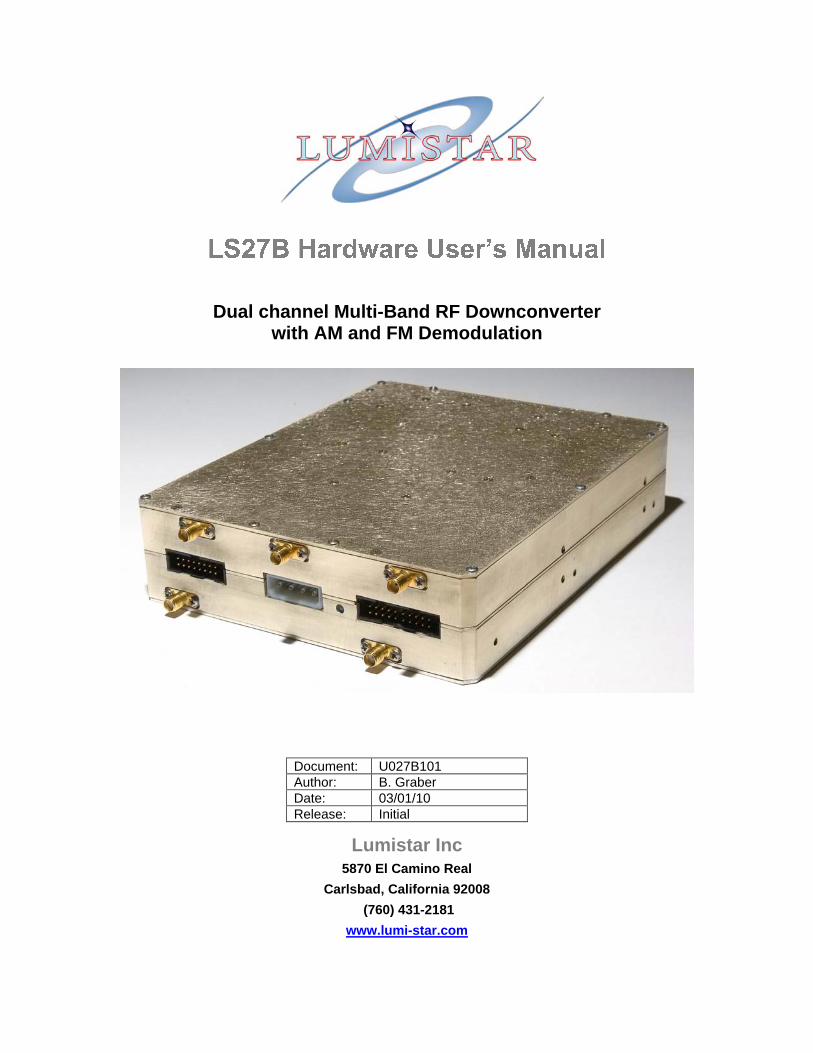
Dual channel Multi-Band RF Downconverterwith AM and FM Demodulation
Lumistar Inc5870 El Camino Real
Carlsbad, California 92008
(760) 431-2181
www.lumi-star.com
Document: U027B101Author: B. GraberDate: 03/01/10Release: Initial

This document is the intellectual property of Lumistar Inc. The document contains proprietary andconfidential information. Reproduction, disclosure, or distribution of this document is prohibited without theexplicit written consent of Lumistar Inc.
This document is provided as is, with no warranties of any kind. Lumistar Inc disclaims and excludes allother warranties and product liability, expressed or implied, including but not limited to any impliedwarranties of merchantability or fitness for a particular purpose or use, liability for negligence in manufactureor shipment of product, liability for injury to persons or property, or for any incidental, consequential, punitiveor exemplary damages. In no event, will Lumistar Inc, be liable for any lost revenue or profits, or otherindirect, incidental and consequential damages even if Lumistar Inc has been advised of such possibilities,as a result of this document or the usage of items described within. The entire liability of Lumistar Inc shallbe limited to the amount paid for this document and its contents.
RESTRICTED RIGHTS LEGEND
Use, duplication, or disclosure by the Government is subject to restrictions set forth in subparagraph (c)(1)(ii)of the rights in Technical Data and Computer Software clause in DFARS 252.227-7013.
Lumistar Inc and its logo are trademarks of Lumistar Inc. All other brand names and product namescontained in this document are trademarks, registered trademarks, or trade names of their respectiveholders.
© 2010 Lumistar Inc. All rights reserved.
Lumistar Inc5870 El Camino RealCarlsbad, CA 92008(760) 431-2181(760) 431-2665 Faxwww.lumi-star.com

LS27B Hardware User’s Manual
U027B101 Lumistar Inc. Page 303/12/10
TABLE OF CONTENTS
1 INTRODUCTION..................................................................................................................... 5
1.2 MANUAL FORMAT AND CONVENTIONS .................................................................................. 5
2 THEORY OF OPERATION..................................................................................................... 9
2.1 1ST
DOWNCONVERSION ....................................................................................................... 92.2 1
STIF BAND-PASS FILTER ................................................................................................... 9
2.3 1ST
LOCAL OSCILLATOR....................................................................................................... 92.4 2
NDDOWNCONVERSION..................................................................................................... 10
2.5 2ND
LOCAL OSCILLATOR .................................................................................................... 102.6 2
NDIF FILTER ................................................................................................................... 10
2.7 DIGITAL AGC/LIMITING AMPLIFICATION/AM DEMODULATION ............................................... 102.8 DIGITAL SIGNAL PROCESSING ENGINE (DSPE).................................................................. 102.9 FM DEMODULATION STAGE (OPTIONAL) ............................................................................ 10
3 INSTALLATION AND CONFIGURATION................................................................................ 11
3.1 PRODUCT OUTLINE DIAGRAMS .......................................................................................... 113.2 HARDWARE CONFIGURATION ............................................................................................ 113.3 PHYSICAL INSTALLATION ................................................................................................... 153.4 INTERCONNECTION ........................................................................................................... 173.5 EXTERNAL SETUP DISCRETES........................................................................................... 21
4 COMMUNICATIONS ............................................................................................................ 22
4.1 SERIAL BUS INTERFACE .................................................................................................... 224.1.1 SERIAL BUS INTERFACE – DUAL RECEIVER INTERFACE PROTOCOL .................................. 224.1.2 SERIAL BUS INTERFACE – SINGLE RECEIVER INTERFACE PROTOCOL ............................... 22
5 COMMUNICATIONS ............................................................................................................ 23
5.1 SINGLE RECEIVER PROTOCOL........................................................................................... 235.1.1 SINGLE RECEIVER PROTOCOL - COMMAND AND STATUS MESSAGING .............................. 235.1.1.1 SINGLE RECEIVER PROTOCOL - COMMAND MESSAGING .............................................. 265.1.1.1.1 SINGLE RECEIVER PROTOCOL - PING COMMAND .................................................... 265.1.1.1.2 SINGLE RECEIVER PROTOCOL - PRIMARY SETUP COMMAND .................................... 265.1.1.1.3 SINGLE RECEIVER PROTOCOL - SECONDARY SETUP COMMAND ............................... 265.1.1.2 SINGLE RECEIVER PROTOCOL - COMMAND BIT/BYTE DEFINITIONS............................... 275.1.1.3 SINGLE RECEIVER PROTOCOL - STATUS MESSAGING .................................................. 305.1.1.3.1 SINGLE RECEIVER PROTOCOL - PRIMARY STATUS RESPONSE.................................. 305.1.1.3.2 SINGLE RECEIVER PROTOCOL - SECONDARY STATUS RESPONSE............................. 305.1.1.4 SINGLE RECEIVER PROTOCOL - STORED SETUP STATUS RESPONSE............................ 305.1.1.5 SINGLE RECEIVER PROTOCOL - EEPROM PAGE READ STATUS RESPONSE................. 315.1.1.6 SINGLE RECEIVER PROTOCOL - STATUS BIT/BYTE DEFINITIONS................................... 325.2 DUAL RECEIVER PROTOCOL ............................................................................................. 345.2.1 DUAL RECEIVER PROTOCOL - COMMAND AND STATUS MESSAGING ................................. 345.2.1.1 DUAL RECEIVER PROTOCOL - COMMAND MESSAGING ................................................. 375.2.1.1.1 DUAL RECEIVER PROTOCOL - PING COMMAND....................................................... 375.2.1.1.2 DUAL RECEIVER PROTOCOL - PRIMARY SETUP COMMAND ....................................... 375.2.1.1.3 DUAL RECEIVER PROTOCOL - SECONDARY SETUP COMMAND .................................. 375.2.1.2 DUAL RECEIVER PROTOCOL - COMMAND BIT/BYTE DEFINITIONS.................................. 385.2.1.3 DUAL RECEIVER PROTOCOL - STATUS MESSAGING ..................................................... 415.2.1.3.1 DUAL RECEIVER PROTOCOL - PRIMARY STATUS RESPONSE .................................... 415.2.1.3.2 DUAL RECEIVER PROTOCOL - EEPROM PAGE READ STATUS RESPONSE ................ 41

LS27B Hardware User’s Manual
U027B101 Lumistar Inc. Page 403/12/10
5.2.1.4 DUAL RECEIVER PROTOCOL - STATUS BIT/BYTE DEFINITIONS ..................................... 44
LS27B Hardware User’s Manual
U027B101 Lumistar Inc. Page 503/12/10
1 Introduction
1.1 General
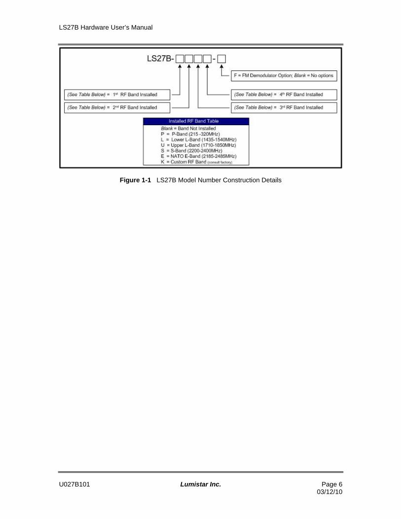
This document is the Hardware User’s Manual for the Lumistar LS27B Dual Channel Multi-bandRF Downconverter. This product represents Lumistar’s 3rd generation of the LS27 Series of DualChannel RF Downconverters. In addition to the functionalities of the Lumistar LS27P3 PCIdownconverter, this product also provides and optional FM demodulation stage for each inputchannel. Figure 1-1 contains detailed model number construction. This document applies to allmodel combinations indicated by this figure.
The intent of this document is to provide physical, functional, and operational information for theend user including hardware configuration, interconnection and software interfaces for the device.
The design implements a Digital Signal Processor Engine (DSPE) controlled superhetrodynedownconverter with AM demodulation and optional FM demodulation. This receiver is in thephysical format and size similar to a standard 5 3/4” CD or DVD drive format. The productprovides two independent and autonomous multi-band downconversion stages. Each channelprovides the conversion of up to four RF pass-bands to a 70MHz Intermediate Frequency (IF)output while providing AM demodulation of the input signal. The product’s standard configurationprovides eight software selectable IF bandwidth filters, roughly placed at octave intervals (or asordered by the customer), to reduce channel noise bandwidth and improve adjacent channelrejection. The product line can optionally be equipped with an FM demodulation stage and eightvideo filters.
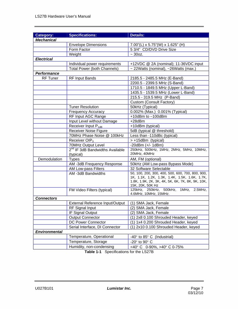
Table 1-1 provides specifications for electrical, mechanical, and operational characteristics of theLS27B product. A block diagram of the product design is shown in Figure 1-2.
1.2 Manual Format and Conventions
This manual contains the following sections:
Chapter 1 provides a brief product overview and technical specifications Chapter 2 provides receiver theory of operation Chapter 3 provides installation and configuration instructions Chapter 4 provides programming information
Throughout this document, several document flags will be utilized to emphasis warnings or otherimportant data. These flags come in three different formats: Warnings, Cautions, andInformation. Examples of these flags appear below.
LS27B Hardware User’s Manual
U027B101 Lumistar Inc. Page 603/12/10
Figure 1-1 LS27B Model Number Construction Details
LS27B Hardware User’s Manual
U027B101 Lumistar Inc. Page 703/12/10
Category: Specifications: Details:Mechanical
Envelope Dimensions 7.00”(L) x 5.75”(W) x 1.625” (H)Form Factor 5 3/4” CD/DVD Drive SizeWeight ~ 30oz.
ElectricalIndividual power requirements +12VDC @ 2A (nominal); 11-36VDC inputTotal Power (both Channels) ~ 22Watts (nominal), ~26Watts (max.)
PerformanceRF Tuner RF Input Bands 2185.5 - 2485.5 MHz (E-Band)
2200.5 - 2399.5 MHz (S-Band)1710.5 - 1849.5 MHz (Upper L-Band)1435.5 - 1539.5 MHz (Lower L-Band)215.5 - 319.5 MHz (P-Band)Custom (Consult Factory)
Tuner Resolution 50kHz (Typical)Frequency Accuracy 0.002% (Max.) 0.001% (Typical)RF Input AGC Range +10dBm to –100dBmInput Level without Damage +28dBmReceiver Input P1dB +10dBm (typical)Receiver Noise Figure 5dB (typical @ threshold)70MHz Phase Noise @ 100kHz Less than -110dBc (typical)Receiver OIP3 > +15dBm (typical)70MHz Output Level -20dBm (+/- 1dBm)2
ndIF 3dB Bandwidths Available
(typical)250kHz, 500kHz, 1MHz, 2MHz, 5MHz, 10MHz,20MHz, 40MHz
Demodulation Types AM, FM (optional)AM -3dB Frequency Response 50kHz (AM Low-pass Bypass Mode)AM Low-pass Filters 32 Software SelectableAM -3dB Bandwidths 50, 100, 200, 300, 400, 500, 600, 700, 800, 900,
1K, 1.1K, 1.2K, 1.3K, 1.4K, 1.5K, 1.6K, 1.7K,1.8K, 1.9K, 2K, 3K, 4K, 5K, 6K, 7K, 8K, 9K, 10K,15K, 20K, 50K Hz
FM Video Filters (typical) 125kHz, 250kHz, 500kHz, 1MHz, 2.5MHz,4.6MHz, 10MHz, 15MHz.
ConnectorsExternal Reference Input/Output (1) SMA Jack, FemaleRF Signal Input (2) SMA Jack, FemaleIF Signal Output (2) SMA Jack, FemaleOutput Connector (1) 2x8 0.100 Shrouded Header, keyedDC Power Connector (1) 1x4 0.200 Shrouded Header, keyedSerial Interface, DI Connector (1) 2x10 0.100 Shrouded Header, keyed
EnvironmentalTemperature, Operational -40 to 85 C (Industrial)Temperature, Storage -20to 90 CHumidity, non-condensing <40 C 0-90%, >40 C 0-75%
Table 1-1 Specifications for the LS27B

LS27B Hardware User’s Manual
U027B101 Lumistar Inc. Page 803/12/10
Figure 1-2 Block Diagram of LS27B Series Multi-band Receiver

LS27B Hardware User’s Manual
U027B101 Lumistar Inc. Page 903/12/10
2 Theory of Operation
In order to more clearly understand the operation of the receiver, this section will detail thevarious stages of the receiver design. These stages are as follows:
- 1st
Downconversion- 1
stIF Band-pass Filter
- 1st
Local Oscillator- 2
ndDownconversion
- 2nd
Local Oscillator- 2
ndIF Filter
- Limiting Amplifier/AM Demodulation/Digital AGC (DAGC)- Digital Signal Processing Engine (DSPE)- FM Demodulation Stage (Optional)
With the exception of the DSPE, each of these sections are physically shielded and isolated fromone another to facilitate the greatest EMI/RFI ingress and egress protection allowing the receiverexceptional performance.
For the following sections, refer to the block diagram of Figure 1-2.
2.1 1st Downconversion
The RF input is applied to the 1st
Downconversion stage. The stage may optionally contain abias-T which can be used to power an external LNA through the RF interface port. (Contact thefactory for further details on this option.) A DAGC section is next in the signal chain for very highlevel signal protection and compression compensation. This is followed by a low-noise amplifier(LNA) to provide a large amount of gain while maintaining a very low noise figure enhancing thereceiver’s overall sensitivity. Selectable RF band-pass filters follow the LNA. The RF signal isthen mixed with the first local oscillator (LO) which converted to the 1
stIF frequency.
2.2 1st IF Band-pass FilterThe output of the 1
stDownconversion stage is send through one of two1
stIF filter paths based on
the selection of high-side or low side conversion. To eliminate images and limit the overall noisebandwidth to the remaining receiver sections, a 50MHz band-pass filter is switched into the signalpath.
2.3 1st Local Oscillator
In a superhetrodyne design, local oscillators (LOs) are utilized to convert high frequencies tolower, “intermediate” frequencies. The first LO is injected into the mixer of the firstDownconversion stage to accomplish this task. Mixers can either utilize a sum or differencefrequency component to produce IF frequencies. For example, if an RF frequency of 2,200 MHzwas to be converted to an intermediate frequency of 250MHz, a difference component of1,950MHz could injected to the mixer or a sum frequency component of 2,450MHz could beapplied. The difference component LO application is referred to a “low-side” conversion. Thesum component application is referred to as “high-side” conversion. Both methods are equallyvalid and each has its own benefits. The LS27B design has the ability to utilize either approachand actually switch between the methods when necessary for performance reasons.

LS27B Hardware User’s Manual
U027B101 Lumistar Inc. Page 1003/12/10
2.4 2nd Downconversion
The receiver designs contain a switchable 2nd
Downconversion stage. Similar to the 1st
Downconversion stage, it contains a mixer to convert the 1st
IF frequency to a second IFfrequency of 70MHz. If the RF frequency band is relatively low, as is the case for P-Band inputs,the on-board processor can bypass the 2
ndDownconversion stage switching to a single
superhetrodyne process. In either case, a low-pass filter is applied to the signal path at the outputof this stage to reduce harmonics and low frequency noise from being applied to subsequentstages.
2.5 2nd Local Oscillator
The second LO is injected into the mixer of the 2nd
Downconversion stage to provide the secondIF frequency of 70MHz. Like the first conversion stage, the second LO utilizes low-side injectionfor this conversion. A low-pass filter is applied to the LO output to minimize spurious andharmonic signals from being converted in the 2
ndDownconversion stage. The 2
ndLO is
automatically disabled for RF bands that employ a single super heterodyne process.
2.6 2nd IF Filter
From the output of the 2nd
conversion stage, the resulting intermediate frequency is then appliedto a group of bandpass filters to minimize noise bandwidth and improve adjacent channelrejection. The 2
ndIF stage contains eight IF (SAW) filters centered at 70MHz and varying in
bandwidth from 250kHz to 40MHz in approximately octave steps.
2.7 Digital AGC/Limiting Amplification/AM Demodulation
Outputs from the 2nd
IF Filter Stage are routed to the final signal detection, AM demodulation, andgain stage in the receiver. The output stage combines both a limiting amplifier and digital AGC(DACG) section. Included in the design is an AM demodulation stage for antenna trackingapplications. The main system gain element provides for 90 to 110dB of signal gain. Signal leveldetection is utilized in DAGC controls.
2.8 Digital Signal Processing Engine (DSPE)
The LS27B design contains a highly integrated digital signal processing engine (DSPE) which isutilized for linearization, filtering and control applications. This engine is composed of a digitalsignal processor, FPGA resources, ADCs, DACs and localized memory used to process thesignal path parameters. Each of the channels is controlled and statused as an autonomousreceiver. The engine performs “real-time” tasks as well as user software interfaces.
2.9 FM Demodulation Stage (Optional)The LS27B design may optionally contain an FM demodulation stage for each channel. The stageis split between a narrow-band and wide-band demodulator to optimize processing of each signalcharacteristic. The output of the FM demodulation is software switched between one of eightvideo filters. The output can also be switched, in addition to the video filter, thru a video de-emphasis network for true analog video signals. The unit is comes standard with NTSC de-emphasis but other formats are available. The demodulation stage has a software adjustableoutput level.
LS27B Hardware User’s Manual
U027B101 Lumistar Inc. Page 1103/12/10
3 Installation and Configuration
Chapter 3 provides installation and configuration information. This chapter will familiarize theuser with the layout of the device, and provide information on the proper installation andinterconnection of the hardware.
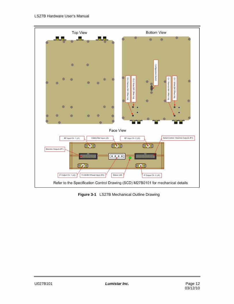
3.1 Product Outline Diagrams
Figure 3-1 contains an outline diagram of the top and bottom sides of the product. Connectorlocations and switch positions are indicated. The model number, serial number, revisioninformation and product options are denoted on the RF enclosure label.
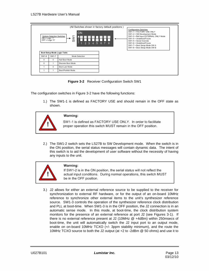
3.2 Hardware Configuration
The receiver design contains configuration switches to control various functions. Figure 3-2contains a diagram of the configuration switches along with the default factory positions for theseswitches.
LS27B Hardware User’s Manual
U027B101 Lumistar Inc. Page 1203/12/10
Figure 3-1 LS27B Mechanical Outline Drawing
LS27B Hardware User’s Manual
U027B101 Lumistar Inc. Page 1303/12/10
Figure 3-2 Receiver Configuration Switch SW1
The configuration switches in Figure 3-2 have the following functions:
1.) The SW1-1 is defined as FACTORY USE and should remain in the OFF state asshown.
2.) The SW1-2 switch sets the LS27B to SW Development mode. When the switch is inthe ON position, the serial status messages will contain dynamic data. The intent ofthis switch is to aid the development of user software without the necessity of havingany inputs to the unit.
3.) J2 allows for either an external reference source to be supplied to the receiver forsynchronization to external RF hardware, or for the output of an on-board 10MHzreference to synchronize other external items to the unit’s synthesizer referencesource. SW1-3 controls the operation of the synthesizer reference clock distributionand PLL at boot-time. When SW1-3 is in the OFF position, the J2 connection is in anautomatic sense mode. In this mode, at boot-time, the clock distribution systemmonitors for the presence of an external reference at port J2 (see Figures 3-1). Ifthere is no external reference present at J2 (10MHz @ +4dBm) within 250msecs ofboot-time, the unit will automatically switch the J2 input port to an output mode,enable on on-board 10MHz TCXO (+/- 3ppm stability minimum), and the route the10MHz TCXO source to both the J2 output (at +2 to -2dBm @ 50 ohms) and use it to
LS27B Hardware User’s Manual
U027B101 Lumistar Inc. Page 1403/12/10
synchronize the internal synthesizers. When SW1-3 is in the ON position, theinternal LS27B 10MHz reference clock will be disabled and the J2 connector will beswitched to be a dedicated input. In this mode, the unit will presume the presence ofan external 10MHz reference source.
4.) Switch SW1-5 initiates the serial override mode. When in the ON position, the serialinterface is automatically set to 57.6K BAUD for each serial communicationschannel. When in the OFF position, commands to alter the serial data rate can beissued.
5.) Switches SW1-7 and SW1-8 define the LS27B power-up boot configurationselection. This combination of switches allows the user to select pre-storedconfiguration setups by various methods. The description of these methods follows:
a. NULL Boot Mode – In this mode, the LS27B receivers will not tune to anystored setups that may have been previously stored in the unit’s internal non-volatile memory. When commanded via one of the appropriate serialinterfaces, it will tune the receiver as commanded. In this mode, storage ofsetup parameters are stored in internal non-volatile memory.
b. Discrete Boot Mode – In this mode, the LS27B receiver will be setups willbe selected via the state of the external discrete lines on P3-7 thru P3-10.These discrete lines will determine a four bit number from zero to fifteen. Atboot time, the LS27B will tune both receivers to the setup whose number isdefined by the values of the discrete lines. Note that each receiver may stillbe tuned to a different frequency and setup, since each receiver has aseparate list of 16 setups. Subsequent serial setup commands will overridethe boot setup and save that setup in non-volatile memory.
c. Boot Last Mode – In this mode LS27B will program the receivers with thelast valid setup. Subsequent setup commands will override the boot setupand replace the setup as directed by the user.
d. Boot Prohibit Mode - This mode is designed for security consciousrequirements. In this state the LS27B will not tune to any setup at power-up.Any serial commands will setup the receivers as usual, but no information willbe retained internally in non-volatile memory. In addition, at boot time anyexisting setup information in any of the sixteen possible setup locations innon-volatile memory will be deleated.
6.) Switches defined as “Undefined/Future” have no implementation and thus their stateis irrelevant.
LS27B Hardware User’s Manual
U027B101 Lumistar Inc. Page 1503/12/10
3.3 Physical Installation
To install the receiver in the target computer system, the following procedure should be followed:
1. Perform a normal system shutdown of the target host system and remove the primarypower plug.
2. Install the receiver in an unobstructed DVD/CD drive bay or in mounting rails. PCs varyin their mechanical configurations so it may be necessary to remove additional PChardware to properly install the unit.
3. For mounting hardware locations, reference the Specification Control Drawing for theproduct (Doc. Number: M27B0101).
4. It is recommended that at least four 4-40UNC mounting screws (provided) be used in themounting of the unit. This accommodates higher vibration and shock environments.Ensure that the installation provides room for the RF and I/O connections.
5. Airflow across the unit is strongly recommended to prevent long-term heat relateddamage. Multiple sets of mounting holes have been provided to allow for some rear fanclearances.
6. Connect the serial control interface to an available RS/EIA-232 interface via the P3connector.
7. Connect the user I/O as desired via the P1 connector (refer to Figure 3-3).
8. Connect the required RF and IF connections via the J-numbered connectors (refer toFigure 3-3).
9. Re-apply power to the unit and initiate the user software to communicate via the serialinterface.

LS27B Hardware User’s Manual
U027B101 Lumistar Inc. Page 1703/12/10
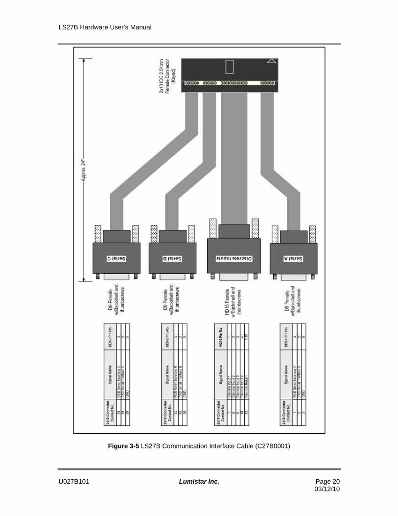
3.4 Interconnection
The receiver platforms provide multiple interface connectors. Figure 3-3 provides interface pin-outs and mating connector information for all connectors. Lumistar can provide an optional BNCstyle interface panel as shown in Figure 3-4 to ease the facilitation of user interfaces. Consult thefactory for further details.
A communication harness is provided with the delivered unit. This harness is shown in Figure 3-5.

LS27B Hardware User’s Manual
U027B101 Lumistar Inc. Page 1803/12/10
Figure 3-3 LS27B Pin-outs and Connector Identification

LS27B Hardware User’s Manual
U027B101 Lumistar Inc. Page 1903/12/10
Figure 3-4 LS27B Optional User Interface Panel
LS27B Hardware User’s Manual
U027B101 Lumistar Inc. Page 2003/12/10
Figure 3-5 LS27B Communication Interface Cable (C27B0001)

LS27B Hardware User’s Manual
U027B101 Lumistar Inc. Page 2103/12/10
3.5 External Setup DiscretesAs shown in Figure 3-3, connector P3 contains five discrete selection inputs (four of which areactive). These bits are used to select previously stored user setups for the LS27B without theuse of a serial host interface.
Each of the LS27B input channels allows the storage of up to sixteen (16) receiver setups. Usingthe serial interface, the user can program particular configurations for the receiver channels, andthen select a corresponding storage number. The operation of these discretes is based on theboot-time mode selection switches of SW1-7 and SW1-8. (Refer to section 3.2 for the propersetting of the configuration switches to enable the use of the external setup discretes.)
The discrete inputs will function as the main controls until serial communications to the unit takesplace. At that point, the discrete interfaces are ignored and control of the unit is switched to theserial interface.
Selection of the discrete (logic 1) is made by connecting the desired discrete input to P3-13 pin.If the discrete input is left disconnected, the input will be considered logic 0.
DIO 4-0 Setting Format Selected0000b Programmed Setup 00001b Programmed Setup 10010b Programmed Setup 20011b Programmed Setup 30100b Programmed Setup 40101b Programmed Setup 50110b Programmed Setup 60111b Programmed Setup 71000b Programmed Setup 81001b Programmed Setup 91010b Programmed Setup 101011b Programmed Setup 111100b Programmed Setup 121101b Programmed Setup 131110b Programmed Setup 141111b Programmed Setup 15
Table 3-1 LS27B External Discrete Setup Selection Table

LS27B Hardware User’s Manual
U027B101 Lumistar Inc. Page 2203/12/10
4 Communications
This chapter provides communications interface information pertaining to the LS27B drive baydual receiver.
4.1Serial Bus Interface
The LS27B is controlled and statused via a standard RS/EIA-232 asynchronous, 3-wire, serialinterface method. The interface is capable of being run at rates between 9.6k BAUD and 115.2kBAUD with a default rate of 57.6k BAUD. The unit is shipped with SW1-5 position in the ONposition. In this position, the unit will only communicate at 57.6k BAUD. (See programmingsection for details on how to alter the serial communication BAUD rate.)
The host communication channel should be setup in the following configuration:Number of bits: 8Parity: NoneStop Bits: 1Flow Control: None
The design contains three serial interface channels, operating via two different protocols: “singlereceiver protocol” and “dual receiver protocol”. Refer to Figure 3-3 for pin-out assignments.
4.1.1 Serial Bus Interface – Dual Receiver Interface Protocol
The Serial “A” bus, contained on P3 pins 1 thru 3, communicates via the “Dual Receiver InterfaceProtocol” defined in chapter 5. This protocol is “enhanced” from the existing “LS25B” protocoland provides for controls for both receiver channels via a single physical interface.
4.1.2 Serial Bus Interface – Single Receiver Interface Protocol
The Serial “B” bus, contained on P3 pins 14 thru 16, and Serial “C” bus, contained on P3 pins 18thru 20, communicates via the existing LS25B Single Receiver Interface Protocol defined inchapter 5. The Serial “B” control/status interface is dedicated to the Channel 1 receiver. TheSerial “C” bus control/status interface is dedicated to Channel 2 receiver.
LS27B Hardware User’s Manual
U027B101 Lumistar Inc. Page 2303/12/10
5 Communications
This chapter provides interface protocol information for the LS27B drive bay dual receiver.
The LS27B product provides a dual protocol interface method. It supports a “single receiverprotocol” which is operational compatible with the previous Lumistar generation of LS25B drive-bay receiver. It also supports an enhanced “dual receiver protocol” which provides someadditional functional capabilities.
5.1 Single Receiver Protocol
Single receiver protocol is active on serial interface B which controls receiver number one of thedevice, and serial interface C, which controls receiver number two. The two receiver interfacescan be operated simultaneously and autonomously. All command/status information contained inthe following sections relates to single channel operation but the format is identical betweenchannels.
5.1.1 Single Receiver Protocol - Command and Status Messaging
Interface using the single receiver protocol is via command-response messaging. For everycommand sent from the host, the receiver will respond to indicate that the command wasreceived. Commands from the host are grouped in two categories: primary commands andsecondary commands. Primary commands are used to control the basic tuning and setup of thereceiver. Secondary commands are used to set various “lower-priority” operational modes and toobtain secondary status. Secondary host commands occasionally require that the host send twocommands: a first command followed by a status request message.
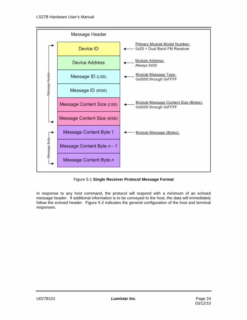
All host messages require a message header of six (6) bytes. If the host command requiresadditional data be transferred to the host, the data will immediately follow the command header.Figure 5-1 contains a diagram of the message header for the single receiver protocol.
The first byte of the message header contains a device identification flag of 0x25. The secondbyte indicates the module address being commanded. For RS-232 communications, this shouldalways be set to 0x00. Bytes 3 and 4 contain the message identification. Message identificationinforms the type and format of data that will follow the header, if any. Bytes 5 and 6 of themessage header indicate the number of command related bytes that follow the message header.
LS27B Hardware User’s Manual
U027B101 Lumistar Inc. Page 2403/12/10
Figure 5-1 Single Receiver Protocol Message Format
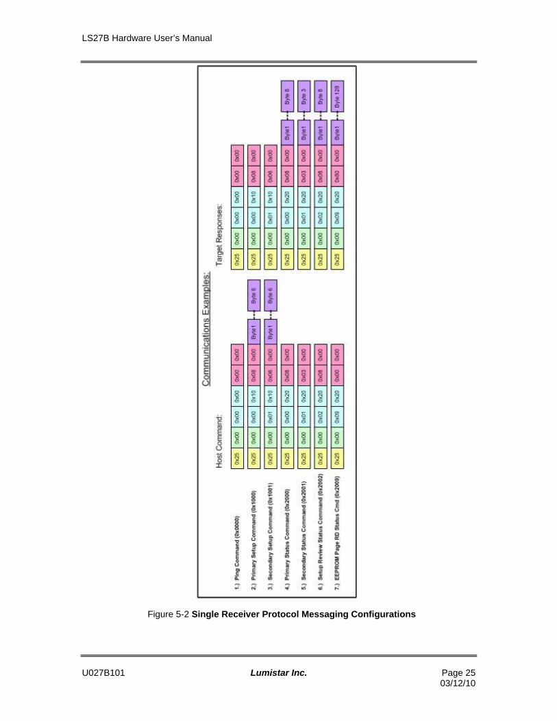
In response to any host command, the protocol will respond with a minimum of an echoedmessage header. If additional information is to be conveyed to the host, the data will immediatelyfollow the echoed header. Figure 5-2 indicates the general configuration of the host and terminalresponses.
LS27B Hardware User’s Manual
U027B101 Lumistar Inc. Page 2503/12/10
Figure 5-2 Single Receiver Protocol Messaging Configurations
LS27B Hardware User’s Manual
U027B101 Lumistar Inc. Page 2603/12/10
5.1.1.1 Single Receiver Protocol - Command Messaging
There are three command message types: a “Ping” command, a “Primary Setup” command, anda “Secondary Setup” command.
5.1.1.1.1 Single Receiver Protocol - PING CommandThe “Ping” command is used as to determine the health/presence of the communications channelbetween the host and the receiver. In response to the “Ping” command, the receiver will echo thereceived message header back to the host.
5.1.1.1.2 Single Receiver Protocol - Primary Setup Command
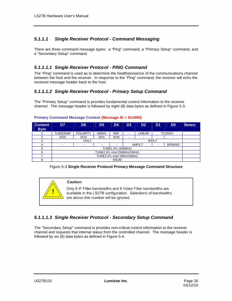
The “Primary Setup” command is provides fundamental control information to the receiverchannel. The message header is followed by eight (8) data bytes as defined in Figure 5-3.
Primary Command Message Content (Message ID = 0x1000)
ContentByte
D7 D6 D5 D4 D3 D2 D1 D0 Notes:
1 TLM2DEMP POLARITY AMINV REF - LINEAR TCONST2 DO3 DO2 DO1 DO0 - - - -3 VFILT IFFILT4 - - - - AMFILT - RFBAND5 TUNE1 (Fc /256MHz)6 TUNE2 (Fc mod 256MHz/1MHz)7 TUNE3 (Fc mod 1MHz/10kHz)8 SNUM
Figure 5-3 Single Receiver Protocol Primary Message Command Structure
5.1.1.1.3 Single Receiver Protocol - Secondary Setup Command
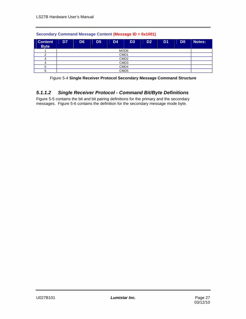
The “Secondary Setup” command is provides non-critical control information to the receiverchannel and requests that internal status from the controlled channel. The message header isfollowed by six (6) data bytes as defined in Figure 5-4.
LS27B Hardware User’s Manual
U027B101 Lumistar Inc. Page 2703/12/10
Secondary Command Message Content (Message ID = 0x1001)
ContentByte
D7 D6 D5 D4 D3 D2 D1 D0 Notes:
1 MODE2 CMD13 CMD24 CMD35 CMD46 CMD5
Figure 5-4 Single Receiver Protocol Secondary Message Command Structure
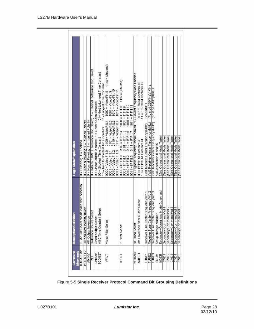
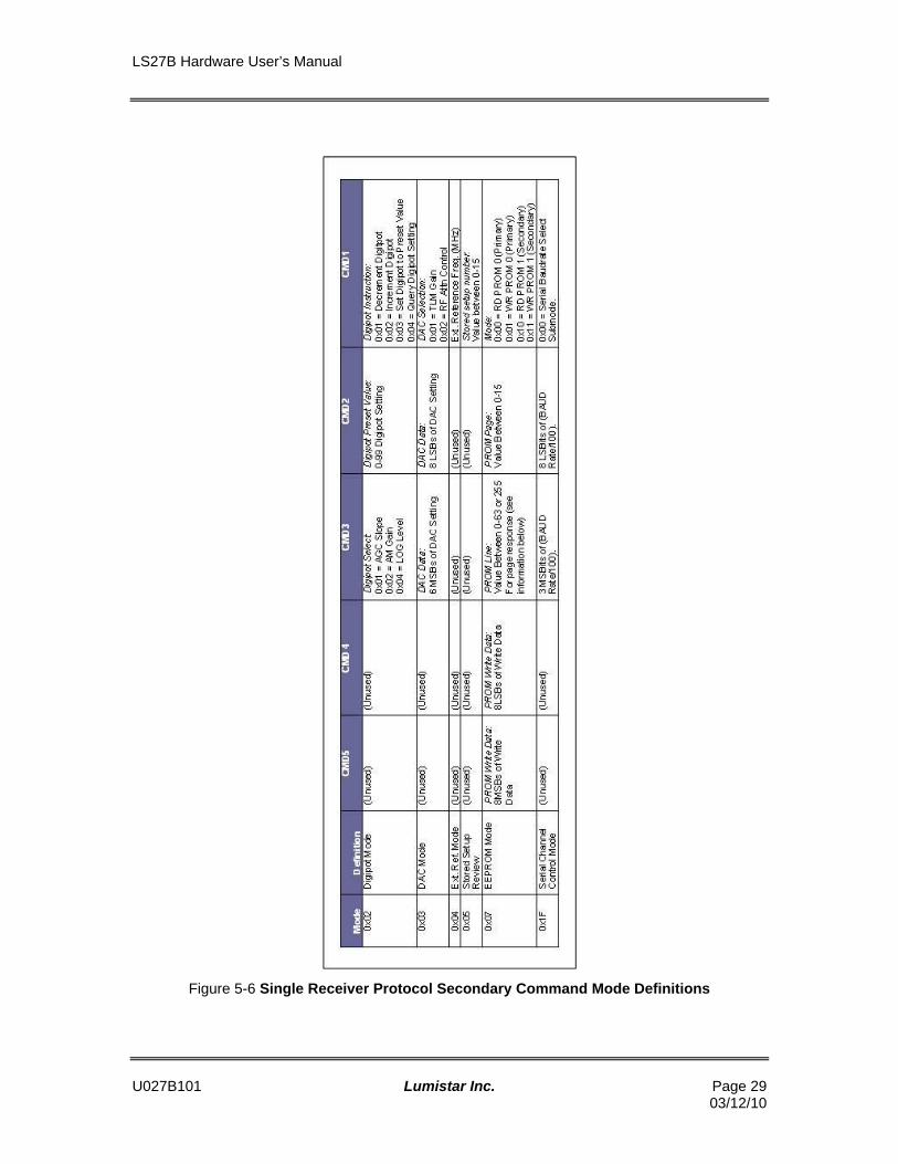
5.1.1.2 Single Receiver Protocol - Command Bit/Byte DefinitionsFigure 5-5 contains the bit and bit pairing definitions for the primary and the secondarymessages. Figure 5-6 contains the definition for the secondary message mode byte.
LS27B Hardware User’s Manual
U027B101 Lumistar Inc. Page 2803/12/10
Figure 5-5 Single Receiver Protocol Command Bit Grouping Definitions
LS27B Hardware User’s Manual
U027B101 Lumistar Inc. Page 2903/12/10
Figure 5-6 Single Receiver Protocol Secondary Command Mode Definitions

LS27B Hardware User’s Manual
U027B101 Lumistar Inc. Page 3003/12/10
5.1.1.3 Single Receiver Protocol - Status Messaging
There are four (4) status message types: primary status response, secondary status response,stored setup status response, and the EEPROM Page read status response.
5.1.1.3.1 Single Receiver Protocol - Primary Status Response
The primary status response provides the host with fundamental receiver status such as thereceived signal strength, FM deviation measurement, AM index value, and the detected AMfrequency. Figure 5-7 depicts the primary status message content.
Primary Status Response Content (Message ID = 0x2000)
ContentByte D7 D6 D5 D4 D3 D2 D1 D0 Notes:
1 - - - - MODID2 RSSI7 RSSII6 RSSI5 RSSI4 RSSI3 RSSI2 RSSI1 RSSI03 - - - - - - RSSI9 RSSI84 DEV5 AMI6 AMFREQ17 AMFREQ28 SNUM
Figure 5-7 Single Receiver Protocol Primary Status Message Structure
5.1.1.3.2 Single Receiver Protocol - Secondary Status Response
The secondary status response provides the receiver with configuration information and providesinformation relates to mode commands. Figure 5-8 depicts the secondary status messagecontent.
Secondary Status Response Content (Message ID = 0x2001)
ContentByte D7 D6 D5 D4 D3 D2 D1 D0 Notes:
1 MODE2 RTN13 RTN2
Figure 5-8 Single Receiver Protocol Secondary Status Message Structure
5.1.1.4 Single Receiver Protocol - Stored Setup Status Response
A total of sixteen (16) receiver setups can be stored in the receiver’s internal memory and then berecalled by simply providing an index value. (Future provisions will allow these setups to beactivated via discrete interaction.) These configurations can be reviewed using secondary modecommands. The stored setup status response message structure is shown in Figure 5-9.

LS27B Hardware User’s Manual
U027B101 Lumistar Inc. Page 3103/12/10
Stored Setup Status Response Content (Message ID = 0x2002)
ContentByte D7 D6 D5 D4 D3 D2 D1 D0 Notes:
1 TLM2DEMP POLARITY AMINV REF - LINEAR TCONST2 - - - - MODID3 VFILT IFFILT4 - - - - AMFILT - RFBAND5 TUNE1 (Fc /256MHz)6 TUNE2 (Fc mod 256MHz/1MHz)7 TUNE3 (Fc mod 1MHz/10kHz)8 SNUM
Figure 5-9 Single Receiver Protocol Stored Setup Status Message Structure
5.1.1.5 Single Receiver Protocol - EEPROM Page Read Status Response
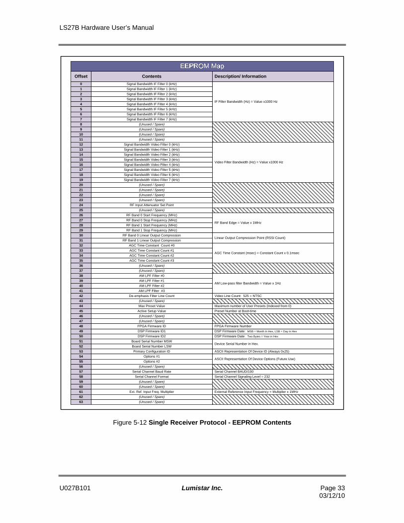
The primary receiver configuration information, used to drive software controls, is found in the firstpage (indexed from 0) of the receivers primary internal EEPROM. Information contained in thisEEPROM includes the bandwidths installed in the receiver, associated IF and video filterbandwidths, along with various other configuration information. This information can beaccessed via an EEPROM read mode command. The resulting status message contents areshown in the Figure 5-10. An example of the EEPROM contents is shown in Figure 5-12.
EEPROM Page Read Response Content (Message ID = 0x2009)
ContentByte D7 D6 D5 D4 D3 D2 D1 D0 Notes:
1 LOC0_LSB2 LOC0_MSB… … More bytes
127 LOC63_LSB128 LOC63_MSB
Figure 5-10 Single Receiver Protocol EEPROM Page Read Status Message Structure

LS27B Hardware User’s Manual
U027B101 Lumistar Inc. Page 3203/12/10
5.1.1.6 Single Receiver Protocol - Status Bit/Byte Definitions
Figure 5-11 contains the bit and bit pairing definitions for the status messages.
Figure 5-11 Single Receiver Protocol Status Response Bit Grouping Definitions
LS27B Hardware User’s Manual
U027B101 Lumistar Inc. Page 3303/12/10
0
Offset
1
2
3
4
5
6
7
8
9
10
11
12
13
14
15
16
17
18
IF Filter Bandwidth (Hz) = Value x1000 Hz
Description/ Information
AGC Time Constant (msec) = Constant Count x 0.1msec
19
20
RF Band Edge = Value x 1MHz
21
22
23
24
25
26
27
28
29
30
31
32
33
34
35
36
37
38
39
40
41
42
43
44
45
46
Serial Channel BAUD/100
47
48
49
50
DSP Firmware Date: MSB = Month in Hex, LSB = Day in Hex
DSP Firmware Date: Two Bytes = Year in Hex
51
56
57
58
59
60
61
62
63
ASCII Representation Of Device ID (Always 0x25)
55
54
53
52
External Reference Input Frequency = Multiplier x 1MHz
Device Serial Number in Hex.
Linear Output Compression Point (RSSI Count)
Video Filter Bandwidth (Hz) = Value x1000 Hz
Signal Bandwidth IF Filter 0 (kHz)
Contents
Signal Bandwidth IF Filter 1 (kHz)
Signal Bandwidth IF Filter 2 (kHz)
Signal Bandwidth IF Filter 3 (kHz)
Signal Bandwidth IF Filter 4 (kHz)
Signal Bandwidth IF Filter 5 (kHz)
Signal Bandwidth IF Filter 6 (kHz)
Signal Bandwidth IF Filter 7 (kHz)
Serial Channel Baud Rate
DSP Firmware ID1
DSP Firmware ID2
Primary Configuration ID
Board Serial Number MSW
Board Serial Number LSW
Ext. Ref. Input Freq. Multiplier
AGC Time Constant Count #0
AGC Time Constant Count #1
AGC Time Constant Count #2
AGC Time Constant Count #3
(Unused / Spare)
(Unused / Spare)
(Unused / Spare)
(Unused / Spare)
RF Band 0 Start Frequency (MHz)
RF Band 0 Stop Frequency (MHz)
RF Band 1 Start Frequency (MHz)
RF Band 1 Stop Frequency (MHz)
(Unused / Spare)
(Unused / Spare)
Signal Bandwidth Video Filter 0 (kHz)
Signal Bandwidth Video Filter 1 (kHz)
Signal Bandwidth Video Filter 2 (kHz)
Signal Bandwidth Video Filter 3 (kHz)
Signal Bandwidth Video Filter 4 (kHz)
Signal Bandwidth Video Filter 5 (kHz)
Signal Bandwidth Video Filter 6 (kHz)
Signal Bandwidth Video Filter 7 (kHz)
(Unused / Spare)
(Unused / Spare)
(Unused / Spare)
(Unused / Spare)
RF Input Attenuator Set Point
(Unused / Spare)
RF Band 0 Linear Output Compression
RF Band 1 Linear Output Compression
AM LPF Filter #0
AM LPF Filter #1
AM LPF Filter #2
AM LPF Filter #3
De-emphasis Filter Line Count
(Unused / Spare)
Max Preset Value
Active Setup Value
(Unused / Spare)
(Unused / Spare)
FPGA Firmware ID
Options #1
Options #2
(Unused / Spare)
Serial Channel Format
(Unused / Spare)
(Unused / Spare)
(Unused / Spare)
(Unused / Spare)
AM Low-pass filter Bandwidth = Value x 1Hz
ASCII Representation Of Device Options (Future Use)
FPGA Firmware Number
Video Line Count: 525 = NTSC
Maximum number of User Presets (Indexed from 0)
Preset Number at Boot-time
Serial Channel Signaling Level = 232
Figure 5-12 Single Receiver Protocol - EEPROM Contents

LS27B Hardware User’s Manual
U027B101 Lumistar Inc. Page 3403/12/10
5.2 Dual Receiver Protocol
Dual receiver protocol is active on serial interface A only. This interface controls both internalreceivers using the same serial interface channel. Each receivers operations are autonomous.
5.2.1 Dual Receiver Protocol - Command and Status Messaging
Interface using the dual receiver protocol is via command-response messaging. For everycommand sent from the host, the receiver will respond to indicate that the command wasreceived. Commands from the host are grouped in two categories: primary commands andsecondary commands. Primary commands are used to control the basic tuning and setup of thereceiver. Secondary commands are used to set various “lower-priority” operational modes and toobtain secondary status. Secondary host commands occasionally require that the host send twocommands: a first command followed by a status request message.
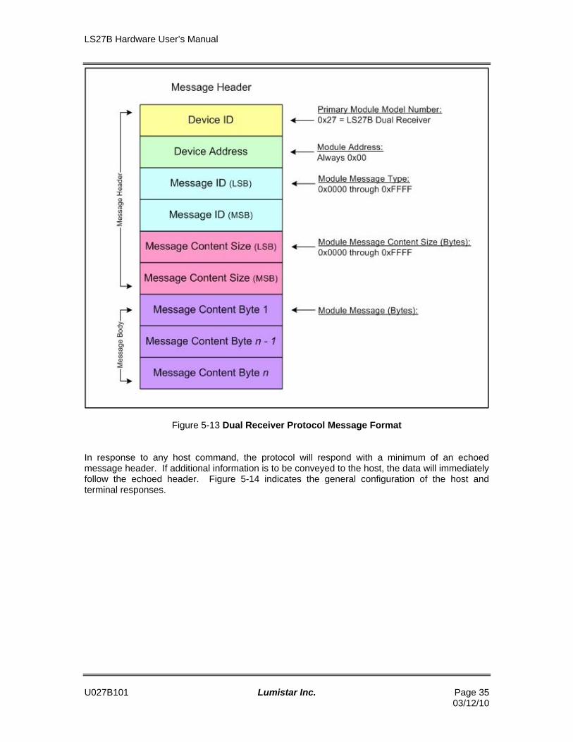
All host messages require a message header of six (6) bytes. If the host command requiresadditional data be transferred to the host, the data will immediately follow the command header.Figure 5-13 contains a diagram of the message header for the dual receiver protocol.
The first byte of the message header contains a device identification flag of 0x27. The secondbyte indicates the module address being commanded which should always be set to 0x00. Bytes3 and 4 contain the message identification. Message identification informs the type and format ofdata that will follow the header, if any. Bytes 5 and 6 of the message header indicate the numberof command related bytes that follow the message header.
LS27B Hardware User’s Manual
U027B101 Lumistar Inc. Page 3503/12/10
Figure 5-13 Dual Receiver Protocol Message Format
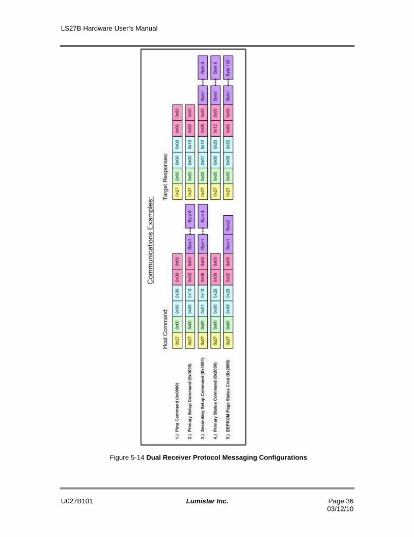
In response to any host command, the protocol will respond with a minimum of an echoedmessage header. If additional information is to be conveyed to the host, the data will immediatelyfollow the echoed header. Figure 5-14 indicates the general configuration of the host andterminal responses.
LS27B Hardware User’s Manual
U027B101 Lumistar Inc. Page 3603/12/10
Figure 5-14 Dual Receiver Protocol Messaging Configurations
LS27B Hardware User’s Manual
U027B101 Lumistar Inc. Page 3703/12/10
5.2.1.1 Dual Receiver Protocol - Command Messaging
There are three command message types: a “Ping” command, a “Primary Setup” command, anda “Secondary Setup” command.
5.2.1.1.1 Dual Receiver Protocol - PING CommandThe “Ping” command is used as to determine the health/presence of the communications channelbetween the host and the receiver. In response to the “Ping” command, the receiver will echo thereceived message header back to the host.
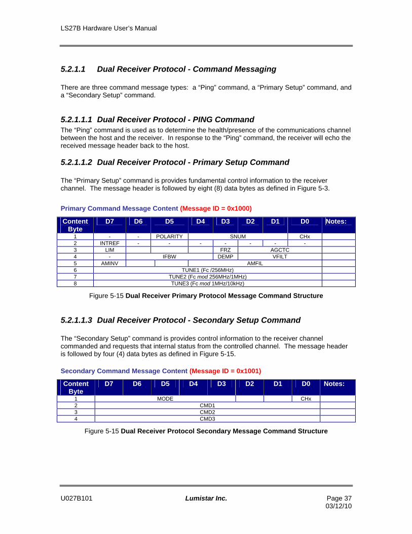
5.2.1.1.2 Dual Receiver Protocol - Primary Setup Command
The “Primary Setup” command is provides fundamental control information to the receiverchannel. The message header is followed by eight (8) data bytes as defined in Figure 5-3.
Primary Command Message Content (Message ID = 0x1000)
ContentByte
D7 D6 D5 D4 D3 D2 D1 D0 Notes:
1 - - POLARITY SNUM CHx2 INTREF - - - - - - -3 LIM FRZ AGCTC4 - IFBW DEMP VFILT5 AMINV AMFIL6 TUNE1 (Fc /256MHz)7 TUNE2 (Fc mod 256MHz/1MHz)8 TUNE3 (Fc mod 1MHz/10kHz)
Figure 5-15 Dual Receiver Primary Protocol Message Command Structure
5.2.1.1.3 Dual Receiver Protocol - Secondary Setup Command
The “Secondary Setup” command is provides control information to the receiver channelcommanded and requests that internal status from the controlled channel. The message headeris followed by four (4) data bytes as defined in Figure 5-15.
Secondary Command Message Content (Message ID = 0x1001)
ContentByte
D7 D6 D5 D4 D3 D2 D1 D0 Notes:
1 MODE CHx2 CMD13 CMD24 CMD3
Figure 5-15 Dual Receiver Protocol Secondary Message Command Structure
LS27B Hardware User’s Manual
U027B101 Lumistar Inc. Page 3803/12/10
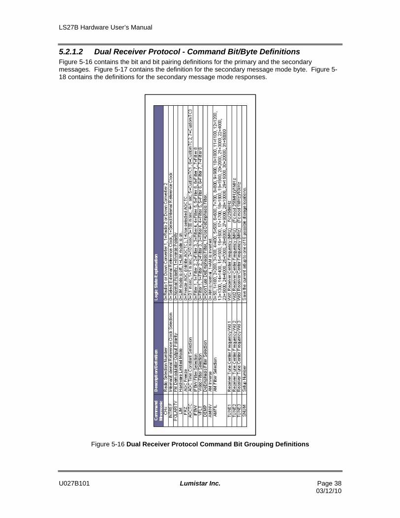
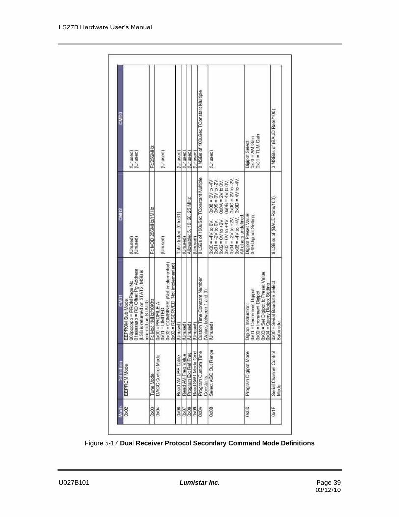
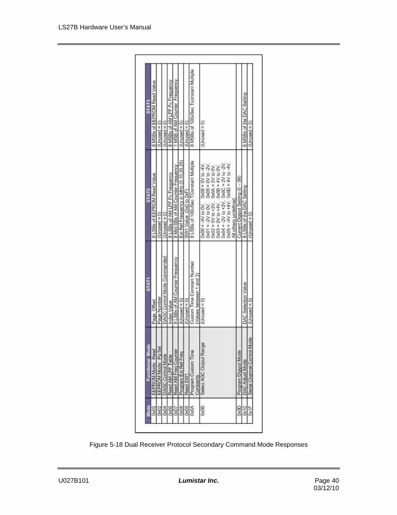
5.2.1.2 Dual Receiver Protocol - Command Bit/Byte DefinitionsFigure 5-16 contains the bit and bit pairing definitions for the primary and the secondarymessages. Figure 5-17 contains the definition for the secondary message mode byte. Figure 5-18 contains the definitions for the secondary message mode responses.
Figure 5-16 Dual Receiver Protocol Command Bit Grouping Definitions
LS27B Hardware User’s Manual
U027B101 Lumistar Inc. Page 3903/12/10
Figure 5-17 Dual Receiver Protocol Secondary Command Mode Definitions
LS27B Hardware User’s Manual
U027B101 Lumistar Inc. Page 4003/12/10
Figure 5-18 Dual Receiver Protocol Secondary Command Mode Responses
LS27B Hardware User’s Manual
U027B101 Lumistar Inc. Page 4103/12/10
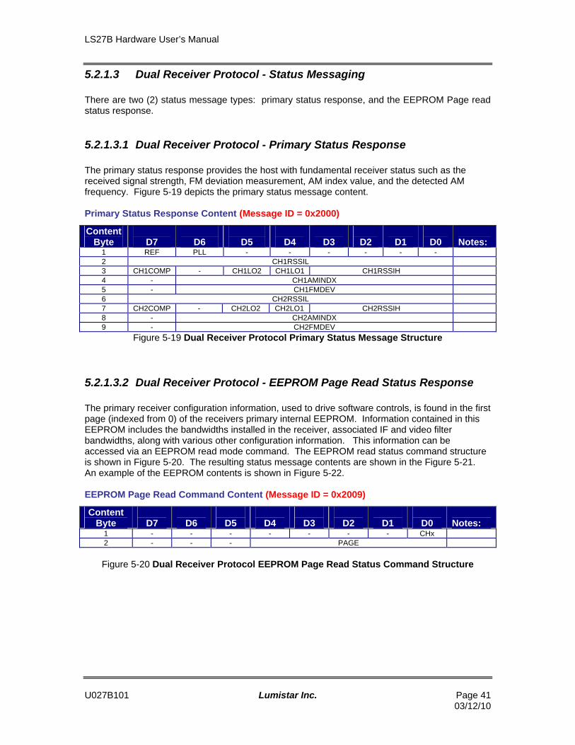
5.2.1.3 Dual Receiver Protocol - Status Messaging
There are two (2) status message types: primary status response, and the EEPROM Page readstatus response.
5.2.1.3.1 Dual Receiver Protocol - Primary Status Response
The primary status response provides the host with fundamental receiver status such as thereceived signal strength, FM deviation measurement, AM index value, and the detected AMfrequency. Figure 5-19 depicts the primary status message content.
Primary Status Response Content (Message ID = 0x2000)
ContentByte D7 D6 D5 D4 D3 D2 D1 D0 Notes:
1 REF PLL - - - - - -2 CH1RSSIL3 CH1COMP - CH1LO2 CH1LO1 CH1RSSIH4 - CH1AMINDX5 - CH1FMDEV6 CH2RSSIL7 CH2COMP - CH2LO2 CH2LO1 CH2RSSIH8 - CH2AMINDX9 - CH2FMDEV
Figure 5-19 Dual Receiver Protocol Primary Status Message Structure
5.2.1.3.2 Dual Receiver Protocol - EEPROM Page Read Status Response
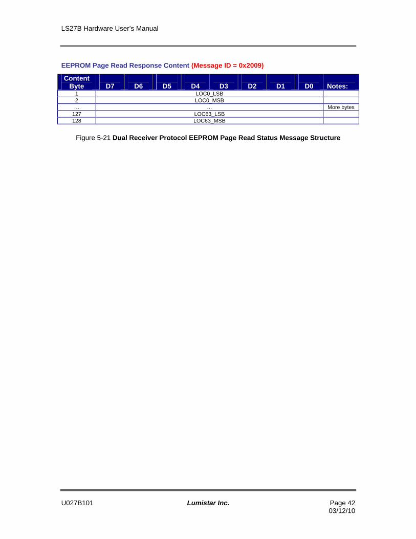
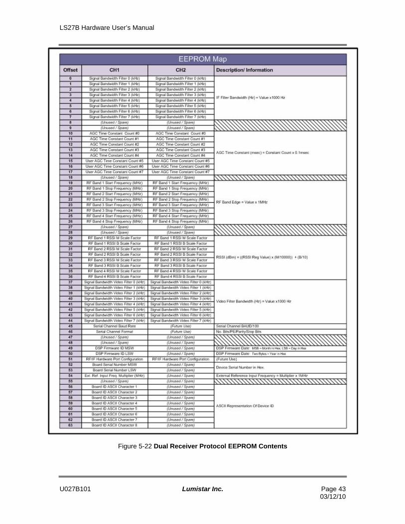
The primary receiver configuration information, used to drive software controls, is found in the firstpage (indexed from 0) of the receivers primary internal EEPROM. Information contained in thisEEPROM includes the bandwidths installed in the receiver, associated IF and video filterbandwidths, along with various other configuration information. This information can beaccessed via an EEPROM read mode command. The EEPROM read status command structureis shown in Figure 5-20. The resulting status message contents are shown in the Figure 5-21.An example of the EEPROM contents is shown in Figure 5-22.
EEPROM Page Read Command Content (Message ID = 0x2009)
ContentByte D7 D6 D5 D4 D3 D2 D1 D0 Notes:
1 - - - - - - - CHx2 - - - PAGE
Figure 5-20 Dual Receiver Protocol EEPROM Page Read Status Command Structure
LS27B Hardware User’s Manual
U027B101 Lumistar Inc. Page 4203/12/10
EEPROM Page Read Response Content (Message ID = 0x2009)
ContentByte D7 D6 D5 D4 D3 D2 D1 D0 Notes:
1 LOC0_LSB2 LOC0_MSB… … More bytes
127 LOC63_LSB128 LOC63_MSB
Figure 5-21 Dual Receiver Protocol EEPROM Page Read Status Message Structure
LS27B Hardware User’s Manual
U027B101 Lumistar Inc. Page 4303/12/10
Figure 5-22 Dual Receiver Protocol EEPROM Contents
LS27B Hardware User’s Manual
U027B101 Lumistar Inc. Page 4403/12/10
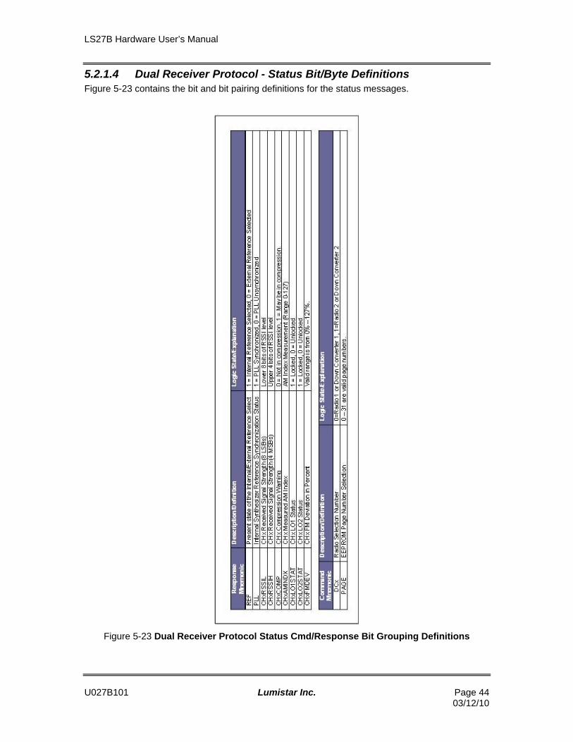
5.2.1.4 Dual Receiver Protocol - Status Bit/Byte DefinitionsFigure 5-23 contains the bit and bit pairing definitions for the status messages.
Figure 5-23 Dual Receiver Protocol Status Cmd/Response Bit Grouping Definitions