dynamic biasing for improved on-orbit total-dose lifetimes
TRANSCRIPT

Dynamic Biasing for Improved On-Orbit Total-Dose Lifetimes ofDynamic Biasing for Improved On-Orbit Total-Dose Lifetimes ofCommercial Semiconductor DevicesCommercial Semiconductor DevicesThis paper was downloaded from TechRxiv (https://www.techrxiv.org).
LICENSE
CC BY-NC-SA 4.0
SUBMISSION DATE / POSTED DATE
31-03-2021 / 05-04-2021
CITATION
Holliday, Maximillian; Heuser, Thomas; Manchester, Zachary; Senesky, Debbie (2021): Dynamic Biasing forImproved On-Orbit Total-Dose Lifetimes of Commercial Semiconductor Devices. TechRxiv. Preprint.https://doi.org/10.36227/techrxiv.14346839.v1
DOI
10.36227/techrxiv.14346839.v1

1
Dynamic Biasing for Improved On-Orbit Total-DoseLifetimes of Commercial Semiconductor Devices
Maximillian Holliday, Thomas A. Heuser, Zachary Manchester, Debbie G. Senesky
Abstract—The survivability of microelectronic devices in ion-izing radiation environments drives spacecraft design, capability,mission-scope, and cost. This work exploits the periodic na-ture of many space radiation environments to extend devicelifetimes without additional shielding or modifications to thesemiconductor architecture. To improve component lifetimes viareduced total-dose accumulation, device bias was modulatedduring periods of intense irradiation. Simulation of this “dynamicbiasing” technique applied to single-transistor devices in a typicallow-Earth orbit results in an increase of component life from5 days to 80 days (16x improvement) at the expense of 8%down time (92% duty cycle). The biasing technique is alsoexperimentally demonstrated using gamma radiation to study twodevice types spanning a range of integrated circuit complexity in109 rad/min and 256 rad/min dose rate conditions. The significantimprovements in device lifetimes demonstrated with the proposeddynamic biasing technique lays a foundation for more effectiveuse of modern microelectronics for space applications. Analogousto the role real-time temperature monitoring plays in maximizingmodern processor performance, the proposed dynamic biasingtechnique is a means of intelligently responding to the radia-tion environment and capable of becoming an integral tool inoptimizing component lifetimes in space.
Index Terms—Charge carrier processes, consumer electronics,degradation, large scale integration, MOSFET, radiation effects,radiation inducted charge neutralization, total ionizing dose
I. INTRODUCTION
THE bias condition of microelectronics during irradiationis known to play a significant role in the impact total
ionizing dose (TID) has on device lifetime [1], [2]. However,aside from niche work investigating optimal device-specificbias states [3], [4], literature is lacking a fundamental studyinto using active device bias configuration as a means ofmitigating device degradation due to TID, thereby extendingdevice lifetimes in radiation environments.
The relationship between device bias and radiation-induceddegradation is well-studied, and can be briefly summarized asan electrostatic potential across a dielectric region causing lessrecombination of radiation-induced electron/hole (e/h) pairs[5]. The electrostatic forces combined with vast differencesin oxide carrier mobilities results in an increase of trappedcharges that is directly dependent on the electric field, oxidetype, and oxide thickness [6]. It is an accumulation of thesetrapped charges inside microelectronics that causes the gradual
M. H. and T.H. Authors are with the Department of Materials Science andEngineering, Stanford University, Stanford, California 94305, USA.
Z. M. Author was with Stanford University, Stanford, California 94305,USA. He is now with the Robotics Institute, Carnegie Mellon University,Pittsburgh, PA 15213 USA.
D. S. Author is with Department of Aeronautics and Astronautics, StanfordUniversity, Stanford, California 94305, USA.
degradation of device performance as a function of TID,ultimately resulting in permanent failure of the device.
For field-effect transistors, TID degradation commonlymanifests as positive or negative shifts in threshold voltage(∆VTH ) as a result of charge trapping [7]. The ∆VTH
formed by radiation-induced trapped charges has many simi-larities to traditional metal-oxide-semiconductor (MOS) agingmechanisms such as hot-electron-induced (HIT) and posi-tive/negative bias temperature instability (PBTI, NBTI) [8],[9]. In both cases, sensitive oxide regions, such as thoselocated at the gate, isolation, and below the substrate arethe primary contributors to the ∆VTH . However, the re-gions of oxide vulnerable to charge trapping and the rate atwhich charge accumulation occurs helps distinguish radiation-induced degradation from those of physical aging.
In the case of TID degradation, the magnitude of ∆VTH
can be estimated by the accumulated dose inside sensitiveoxide regions [2]. Beginning with a simple approximation ofMOSFET device behavior, the threshold voltage (VTH ) canbe described as proportional to the charge of the gate oxide(Qox), and inversely proportional to gate oxide capacitance(Cox). This relationship between VTH and oxide charge allowsfor an estimation of ∆VTH as a function of radiation dose asdescribed by Krantz [10]
∆VTH = V 0TH −
1
Cox
∫ tox
0
f(Eox)Dg0tox
(1− x
tox
)dx
(1)where V 0
TH is the threshold voltage before irradiation, tox isthe thickness of the gate oxide, f(Eox) is the hole yield, Dis the dose (rad) deposited into the material, g0 is the e/h pairper rad (pairs/cm3), and x is the distance in to the oxide.Device bias influences the hole yield term in (1) according tothe relationship
f(Eox) =
(1 +
0.55
| E |
)−0.7
(2)
where E is the electric field in MV/cm across the gatedielectric. Equation (2) describing hole yield has been empir-ically determined and is limited to describing the fraction ofunrecombined holes persisting in SiO2 from Co-60 generatedgamma exposure [11]. Therefore, the hole yield is dependenton the dielectric material, ionizing radiation type, and themagnitude of electric field present in the material.
The usefulness of dynamically changing device bias toextend component lifetimes is well illustrated in the contextof Earth’s orbital radiation environment. To aid in visualizing

2
0 4 8 12 16 20 24
0
5
10
15
20
Time in Orbit (hrs)
Thre
shold
Volt
age
Shif
t
∆V
TH
(nV
)
Dynamic Bias
Reduces Device
Degradation by 16x
Biased (Always On)
Unbiased (Always Off)
Dynamic Biased
0
2
4
6
Do
seR
ate
(mra
d/s
)
Unbiased
Dynamic
Biased
Fig. 1: Simulated 24 hr on-orbit dose rate time series (top) illustrating periodic radiation environment and resulting ∆VTH
(bottom) for a 0.5 mm Al-shielded P-channel MOSFET biased continuously (bottom, blue, VDS = -3.3V), never (bottom,yellow, VDS = 0V), and dynamically (bottom, black, VDS = 0 to -3.3V). Biasing state as a function of orbit time is illustratedfor for all three conditions (middle) resulting in a 16x reduction in ∆VTH , thereby improving the TID lifetime of the simulateddevice by 16x at the expense of 8% down time (92% duty cycle).
the periodic nature of ionizing dose accumulation in satellites,the total dose inside a simple spacecraft occupying a commonlow-Earth orbit (LEO) has been modeled in Fig. 1. As shown,a typical LEO satellite orbiting at an altitude similar to theInternational Space Station (408 km) will experience brief butintense moments of high dose rate irradiation that are separatedby longer periods of little-to-no trapped-particle activity. Thesetransient high dose rate events occur on intervals equal toa typical orbital period for LEO objects (about 90 minutes)and frequently last for minutes, making the transient radiationenvironment ideal for potential dynamic biasing benefits.
This work studied a “dynamic biasing” scheme for devicesas a means of controlling radiation-induced carrier lifetimesand the resulting impact on device degradation for commercialfield-effect devices. Simulations using (1) and (2) were inte-grated into modern trapped-particle models to generate ∆VTH
predictions, then experimentally verified for two commercialdevices that span a wide range of integrated circuit complexity.In-situ measurements collected during radiation testing arepresented for a variety of bias conditions to illustrate theeffectiveness of the proposed dynamic biasing technique atmitigating TID effects.
II. EXPERIMENTAL DETAILS
A. On-Orbit Simulation Parameters
The proposed dynamic biasing technique was modeled for asimple metal oxide field effect transistor geometry in a typical
low-Earth orbit. The simulated radiation environment wasconstructed using AE9, AP9 models for specifying the trappedenergetic particle and space plasma environment [12]. Thesimulated orbit was propagated using the Kepler J2 model for anominal 408 km orbit using the following orbital elements: aninclination of 97.06°, a right ascension of the ascending nodeof 130.53°, an apogee and perigee altitude of 480 km, and anargument of latitude of 180° for a one year duration occurringfrom January 1, 2015 to January 1, 2016. The SHIELDOSE-2Q model was then used to calculate dose rates from thesimulated orbit for an SiO2 point detector centered inside asolid aluminum sphere of radius 0.5mm [13]. Resulting doserates were integrated on five second intervals to produce a timeseries of total dose data for the simulated mission. Equation(1) was used to calculate an estimated ∆VTH for a simpleP-channel MOSFET with a 100 nm thick SiO2 gate oxide forthe simulated total dose values at various bias conditions.
TABLE I: Experimentally Tested Commercial Devices
PartNumber Description Architecture,
# TransistorsPerformance
MetricIRLML2803
(Infineon)MOSFET
(N-Channel)“HexFET”
1 Transistor ∆VTH
IRLML5103(Infineon)
MOSFET(P-Channel)
“HexFET”1 Transistor ∆VTH
TPS82740(TI)
SwitchingRegulator
SOI> 1000 Transistors
OutputVoltage

3
Fig. 2: Representative J.L. Shepherd and Associates MarkI gamma radiation chamber (left, [15], [16] and in-situ testfixture (right) with Pb/Al shielded data acquisition enclosuresupporting the devices under test.
B. Device Selection
Device functionality as a function of bias condition duringirradiation was studied across two levels of commercial VLSIintegration complexity. Table 1 outlines each device categorywith relevant fabrication technology used, the approximatenumber of transistors in the device, and the performance metricused when reporting radiation tolerance.
General device architecture, fabrication details, and es-timated transistor counts were collected using visible-lightspectroscopy to examine representative samples from each de-vice group. Spectroscopy samples were prepared via chemicaldecapsulation following common failure analysis techniques[14]. Devices were submerged in 96% sulfuric acid at 150°Cfor 20 minutes, then rinsed with acetone and again withdeionized water before collecting micrographs on an Olympusstereo microscope.
C. Radiation Test Environment and Setup
TID testing was performed under constant gamma irradia-tion conditions to achieve total dose accumulations that meetor exceed TID values simple spacecraft might experience aftera multi-year mission in LEO. Testing was conducted followingMIL-STD-883 Method 1019.8 with the exception of a Cs-137 source used in place of Co-60 [17]. A J.L. Shepherd andAssociates Mark I model gamma radiation chamber similarto the instrument shown in Fig. 2 from Brookhaven NationalLaboratory was used at the configurable dose rates of 109 and256 rad/min [15], [16]. Solid-state dosimeters from TyndallNational Institute (Part Number: TD1003, 200 µm “radFETs”)were used for in-situ dose characterization.
Separate electrical measurements were necessary to moni-tor the performance metrics of each device during radiationexposure. Aside from the devices under test, all data loggingequipment was housed inside the shielded enclosure shown
Fig. 3: Modular in-situ data acquisition hardware setup usedto operate and monitor device samples during irradiationfeaturing (A) power monitoring and MOSFET switching arraymodule, (B) primary computing and data storage module, and(C) two instances of a versitle 28-bit ADC module driving andmeasuring custom wirebonded devices (left) and a MOSFETdosimeter (right).
in Fig. 2 and constructed of layered aluminum, lead, andpolyethylene terephthalate glycol (PETG) with thicknessesof 1.6 mm, 6.4 mm, and 2 mm, respectively. Attenuationperformance of the shielded enclosure was monitored using aTD1003 radFET located in the center of the shielded volumewhich verified the cumulative dose remained below 100 radthroughout the duration of each experiment.
Figure 3 depicts the open-source data acquisition hardwaredeveloped and used to conduct electrical measurements, in-situ, during irradiation. The modular hardware design enabledoperation and monitoring of the simple transistor devicesand dosimeters as well as the highly integrated switchingregulators while maintaining a form factor suitable for theshielded enclosure. Shown in Fig. 3 is the primary comput-ing module (middle) utilizing a 32-bit ARM microcontroller(Part Number: Microchip ATSAMD51J20A) with on-boardmicroSD socket and external power management, as well amezzanine board (top) containing an array of four MOSFETswitches and power monitoring capability. Illustrated at thebottom of Fig. 3, is a carrier board capable of housingbare die wirebonded to pads (not used in this study) aswell as common surface mount packages (SOT-23, SOT-363)while utilizing a versatile 28-bit analog-to-digital converter(Part Number: TI ADS124S08) to drive devices under testvia the on-chip programmable current sources, voltage ref-erences, temperature sensor, and general purpose I/O. Power

4
5V
100µA
1 MΩ
Q2VTH
5V
100µA
1 MΩ
Q1VTH
Fig. 4: Direct VTH readout circuit for commercial P-Channel(left) and N-Channel (right) MOSFET devices using an exter-nal current source.
to the acquisition hardware was supplied from lithium ioncells (Part Number: LG INR1860 MJ1 3500 mAh) housedinside the shielded enclosure. Schematics, design files, andmanufacturing materials are available on the author’s GitHubfor the processing module: https://github.com/maholli/SAM32,and ADC module: https://github.com/maholli/XTB.
D. Device Operation and VTH Measurement Technique
Threshold voltage was monitored during irradiation forcommercial single-transistor P-channel and N-channel devicesusing the direct VTH readout circuit shown in Fig. 4. TheVTH readout method used is similar to the method describedby Andjelkovic et al. for using MOSFETs as dosimeters [18].Rather than using Andjelkovic’s method of driving currentinto the bulk of the device, which is not always feasiblewith commercially packaged devices, Fig. 4 illustrates ouradaptation that allows current to be driven into the source(internally shorted to the bulk) for PMOS devices, or the drainfor NMOS devices. Additionally, our adaptation includes a 1MΩ resistor connected between the gate contact and ground(PMOS) or the gate contact and drain (NMOS) in order toachieve proper VGS bias with limited gate leakage. Principalof operation for the simple circuits shown in Fig. 4 as directVTH measurement tools relies on the inherent nature of thecurrent source to continuously adjust the voltage necessary todrive the desired current. As configured, the supplied currentmust flow through the channel of the MOSFET which isonly possible once the device’s VTH has been met and thetransistor turns on. For the circuits shown in Fig. 4, VTH ismet as soon as the current source reaches a voltage adequateto achieve the 100 µA output, thereby turning on the tran-sistor Q1 or Q2 and also providing a convenient location fordirect measurement of the the potential (shown in red). Usingthis technique, biased MOSFET samples were continuouslydriven at constant current throughout irradiation with voltagemeasurements performed at a frequency of 0.1 Hz. UnbiasedMOSFET samples had source and drain contacts groundedduring irradiation aside from a 0.5 second configuration andmeasurement routine performed at a frequency of 0.1 Hz. Inboth sample groups, the current source within the VTH readout
circuit was configured to drive 100 µA during measurementcollection.
The performance of the heavily-integrated TPS82740switching regulator was quantified by measuring the voltageoutput under a constant load of 10 mA during irradiation.The regulated output voltage is a result of the integrated stepdown converter circuit comprised of thousands of transistorsproviding device features such as control logic, comparators,and voltage references. The devices under test were configuredto output 2.1 V and an array of shielded MOSFET switcheswere used to control regulator input supply according to therelevant duty cycle (75%, 50%, 25%) with a period of 0.016Hz (60 sec).
III. RESULTS AND DISCUSSION
A. On-Orbit Simulation Results
Simulated dose rates as a function of orbit time are shownin Fig. 1 (bottom) for a 24 hour period. The transient doserate spikes are not an artifact of the particle models; rather,the sudden rise in dose rate is caused by localized regionsof trapped electrons and protons present in Earth’s orbit [19].The simulated orbit encounters dose rate spikes on 90-minuteintervals that typically last less than 10 minutes. The resulting∆VTH for the simulated P-channel device are illustrated inFig. 1 (top) for three bias conditions: always biased (blue),never biased (yellow), and dynamically biased (black). Thetotal ∆VTH for the 24 hour period are 19.55 mV, 0.98 mV,and 1.24 mV, respectively. The simulated dynamically biasedcase was powered off for dose rates exceeding 0.001 mrad/sec,resulting in a 16x reduction in ∆VTH as compared to thealways-biased case, at the expense of an 8% reduction in dutycycle (92% time on) for the 24 hour period.
Consider the on-orbit simulation findings applied to a circuitcontaining the modeled P-channel device, exposed to thesimulated on-orbit environment, and able to maintain nominaloperation as long as the respective PMOS device maintainsa VTH tolerance of 10%. Given this scenario, the simulated∆VTH predicts circuit failure after 5.1 days for an always-biased PMOS device, whereas the dynamically biased devicewould extend circuit lifetime to 80.5 days (a 16x, or 1600%improvement).
The dose rate cutoff threshold, chosen as 0.001 mrad/secfor the above simulation, is a powerful means of tuning the
TABLE II: Summary of Experimentally Determined MOSFETand Regulator Radiation Performance
DescriptionPart
Number
Duty
Cycle
Functional
Dose Limit
Lifetime
Improvement
SwitchingRegulator
TPS82740 25% 22 krad
57%TPS82740 50% 22 krad
TPS82740 75% 14 krad
N-ChannelMOSFET
IRLML2803 0% 34 krad13%
IRLML2803 100% 30 krad
P-ChannelMOSFET
IRLML5103 0% 39 krad44%
IRLML5103 100% 27 krad
5
0 5000 10000 15000 20000 25000
0.0
0.2
0.4
0.6
Dose (rad)
Th
resh
old
Vo
ltag
eS
hif
t∆
VT
H(V
)
(a)
Biased (Always On)
Unbiased (Always Off)
0 5000 10000 15000 20000 25000
0.0
0.2
0.4
0.6
Dose (rad)
Thre
shold
Volt
age
Shif
t∆
VT
H(V
)
(b)
Biased (Always On)
Unbiased (Always Off)
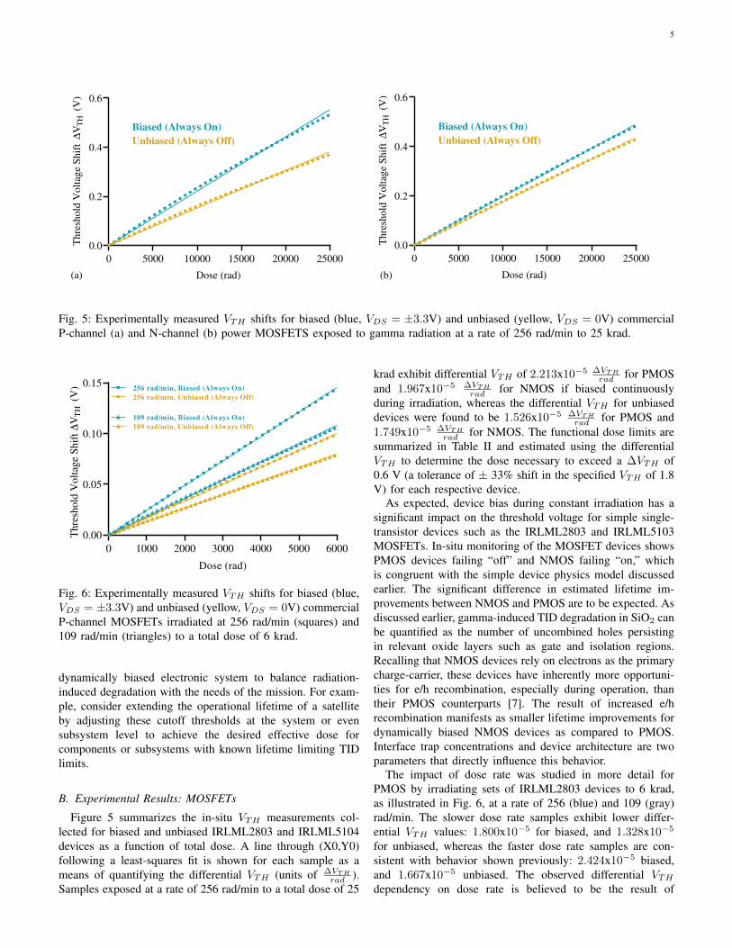
Fig. 5: Experimentally measured VTH shifts for biased (blue, VDS = ±3.3V) and unbiased (yellow, VDS = 0V) commercialP-channel (a) and N-channel (b) power MOSFETS exposed to gamma radiation at a rate of 256 rad/min to 25 krad.
0 1000 2000 3000 4000 5000 6000
0.00
0.05
0.10
0.15
Dose (rad)
Th
resh
old
Vo
ltag
eS
hif
t∆
VT
H(V
)
109 rad/min, Unbiased (Always Off)
109 rad/min, Biased (Always On)
256 rad/min, Biased (Always On)
256 rad/min, Unbiased (Always Off)
Fig. 6: Experimentally measured VTH shifts for biased (blue,VDS = ±3.3V) and unbiased (yellow, VDS = 0V) commercialP-channel MOSFETs irradiated at 256 rad/min (squares) and109 rad/min (triangles) to a total dose of 6 krad.
dynamically biased electronic system to balance radiation-induced degradation with the needs of the mission. For exam-ple, consider extending the operational lifetime of a satelliteby adjusting these cutoff thresholds at the system or evensubsystem level to achieve the desired effective dose forcomponents or subsystems with known lifetime limiting TIDlimits.
B. Experimental Results: MOSFETs
Figure 5 summarizes the in-situ VTH measurements col-lected for biased and unbiased IRLML2803 and IRLML5104devices as a function of total dose. A line through (X0,Y0)following a least-squares fit is shown for each sample as ameans of quantifying the differential VTH (units of ∆VTH
rad ).Samples exposed at a rate of 256 rad/min to a total dose of 25
krad exhibit differential VTH of 2.213x10⁻⁵ ∆VTH
rad for PMOSand 1.967x10⁻⁵ ∆VTH
rad for NMOS if biased continuouslyduring irradiation, whereas the differential VTH for unbiaseddevices were found to be 1.526x10⁻⁵ ∆VTH
rad for PMOS and1.749x10−5 ∆VTH
rad for NMOS. The functional dose limits aresummarized in Table II and estimated using the differentialVTH to determine the dose necessary to exceed a ∆VTH of0.6 V (a tolerance of ± 33% shift in the specified VTH of 1.8V) for each respective device.
As expected, device bias during constant irradiation has asignificant impact on the threshold voltage for simple single-transistor devices such as the IRLML2803 and IRLML5103MOSFETs. In-situ monitoring of the MOSFET devices showsPMOS devices failing “off” and NMOS failing “on,” whichis congruent with the simple device physics model discussedearlier. The significant difference in estimated lifetime im-provements between NMOS and PMOS are to be expected. Asdiscussed earlier, gamma-induced TID degradation in SiO2 canbe quantified as the number of uncombined holes persistingin relevant oxide layers such as gate and isolation regions.Recalling that NMOS devices rely on electrons as the primarycharge-carrier, these devices have inherently more opportuni-ties for e/h recombination, especially during operation, thantheir PMOS counterparts [7]. The result of increased e/hrecombination manifests as smaller lifetime improvements fordynamically biased NMOS devices as compared to PMOS.Interface trap concentrations and device architecture are twoparameters that directly influence this behavior.
The impact of dose rate was studied in more detail forPMOS by irradiating sets of IRLML2803 devices to 6 krad,as illustrated in Fig. 6, at a rate of 256 (blue) and 109 (gray)rad/min. The slower dose rate samples exhibit lower differ-ential VTH values: 1.800x10⁻⁵ for biased, and 1.328x10⁻⁵
for unbiased, whereas the faster dose rate samples are con-sistent with behavior shown previously: 2.424x10⁻⁵ biased,and 1.667x10⁻⁵ unbiased. The observed differential VTH
dependency on dose rate is believed to be the result of

6
0 5000 10000 15000 20000 25000
0
1
2
3
Dose (rad)
Outp
ut
Vo
ltag
e(V
)
2.1V Regulator
Target Voltage
75% Duty Cycle
50% Duty Cycle
25% Duty Cycle
Fig. 7: Output voltage measured in-situ during irradiation forcommercial TPS82740 switching regulators under constant 10mA load as function of dose for red: 75%, green: 50%, andblue: 25% duty cycled devices.
inherent thermal recombination of e/h pairs as described byOldham [20]. Given the constant exposure environment usedfor this dynamic biasing work, the 44% lifetime improvementfor PMOS and 13% improvement for NMOS are expectedto increase in periodic radiation environments such as LEO.These dose rate findings should be an important parameterfor future real-time implementations of the dynamic biasingtechnique.
Extrapolating the linear relationship between threshold volt-age and dose for the 109 rad/min rate illustrated in Fig. 6, itcan be estimated that the IRLML2803 will no longer meet thespecified VTH of 1.8 V ± 33% at an approximate total doseof 33 krad (biased) and 45 krad (unbiased). This is in strongagreement with TID performance reported by O’Bryan [21]of 35 krad for the IRLML2803.
C. Experimental Results: Switching Regulators
Figure 7 illustrates the output voltage performance of theTPS82740 switching regulator under constant 10 mA load asmeasured during irradiation at a rate of 256 rad/min. Thecomplex output behavior observed in Fig. 7 as a result of theirradiation is broken down into three regions and interpretedbelow.
1) The first observed event is a jump in output voltage from2.1 V to 2.3 V seen at about 6.5 krad for all devices. TheTPS82740 regulators use an internal feedback dividernetwork to configure the output voltage to be one ofeight possible values: 1.8 V to 2.6 V in 0.1 V incre-ments. Therefore, the observed jump in output voltageis believed to be a result of a VTH shift in the erroramplifier and/or main comparator of the feedback loopto yield a new set-point to the control logic. Possibleissues with the data acquisition circuit were ruled outafter confirming all internal health checks were validfor the duration for the experiment and verifying thenew output voltage was an intentional feature of the
device. The change in output voltage at 6.5 krad was notconsidered device failure since it is within the operatingparameters of the device.
2) The second event is a sudden drop-out and subsequentrecovery (with overshoot) of output voltage beginningat 14 krad for the 75% duty cycled device. Althoughthere is partial recovery, the drop in output voltage at 14krad was considered to be device failure for this sample.One possible explanation for the interesting recoverybehavior after about 2.4 krad (9.3 minutes at the doserate of 256 rad/min) is a result of the 1.7 MHz switchingfrequency of the regulator design. Rapidly changing biasconditions have been shown to improve recombinationrates [22]. At the 14 krad point of failure, once the outputvoltage has dropped to 1.3 V it is feasible a localizednet-gain of e/h recombination could form as a result ofthe lower bias. The annihilation of these TID inducedtrapped charges is one method for the comparator torecover after a period of time.
3) Finally, the staggered and abrupt failure mode of allthree devices is observed from 19 krad to 22 krad. Thesudden and precise drop in output voltage from 2.3 Vto 0 V suggests this failure mode to be a result oftriggering one or more of the protection features presentin TPS82740 regulator design. For example, radiationinduced VTH shifts in the input control and comparatorsubsystems could readily engage the TPS82740’s under-voltage lockout or logic-controlled enable/disable fea-ture, resulting in the observed voltage cutoff behavior.Separate testing of each functional block comprising theTPS82740 regulator would be necessary, and outsidethe scope of this work, to conclude root cause of theobserved regulator behavior.
Intermittent failures, as seen in the 75% duty cycle case,and non-linear component lifetimes as function of TID areexpected for highly integrated devices with many subsystemssuch as the TPS82740 regulator. However, with a better under-standing of the complex in-situ behavior during irradiation, it’sclear that bias condition continues to impact overall componentlifetime of the heavily integrated switching regulator resultingin an observed 57% improvement for the 50% duty cycle caseas compared to the 75% case.
IV. CONCLUSIONS AND FUTURE WORK
This work establishes the feasibility of using the pro-posed “dynamic biasing” technique as a means of improvingTID lifetimes for commercially available microelectronic de-vices with single-transistor and >1000 transistor complexities.Trapped particle models were used to simulate a 16x improve-ment in on-orbit transistor lifetimes using the proposed biasingtechnique. Simulated results were demonstrated experimen-tally via in-situ device monitoring during gamma irradiationfor two levels of commercial IC complexity. The biasing tech-nique is found to improve single-transistor commercial devicelifetimes by 44% for PMOS and 13% for NMOS, whereasthe lifetime for a heavily integrated switching regulator wasimproved by 57%.

7
Experimental results show dose rate continues to play a role in lifetimes of dynamically biased PMOS and NMOS devices. Continued research is planned to study the effect of dynamic biasing at the multi-component system level, including methods of integrating responsive sensor systems to provide real-time and intelligent response in volatile radiation environments.
V. ACKNOWLEDGMENT
The authors would like to thank Sharmila Bhattacharya and Sergio R. Santa Maria from NASA Ames Research Center, Moffett Field, California, for access to their radiation facilities.
REFERENCES
[1] James R. Schwank, “Basic Mechanisms of Radiation Effects in theNatural Space Radiation Environment,” Tech. Rep., 1994.
[2] D. M. Fleetwood, “Total Ionizing Dose Effects in MOS and Low-Dose-Rate-Sensitive Linear-Bipolar Devices,” IEEE Transactions on NuclearScience, vol. 60, no. 3, pp. 1706–1730, Jun. 2013.
[3] F. Smith and S. Mostert, “Total Ionizing Dose Mitigation by Meansof Reconfigurable FPGA Computing,” Ph.D. dissertation, University ofStellenbosch, Aug. 2007.
[4] C. J. Gonzalez Aguilera, R. G. Vaz, M. B. Oliveira, V. W. Leorato, O. L.Goncalez, and T. R. Balen, “TID Effects on a Data Acquisition SystemWith Design Diversity Redundancy,” IEEE Transactions on NuclearScience, vol. 65, no. 1, pp. 583–590, Jan. 2018.
[5] H. J. Barnaby, “Total-Ionizing-Dose Effects in Modern CMOS Tech-nologies,” IEEE Transactions on Nuclear Science, vol. 53, no. 6, pp.3103–3121, Dec. 2006.
[6] V. V. Orlov, V. A. Felitsyn, and G. I. Zebrev, “Compact modeling of I-Vcharacteristics in irradiated MOSFETs: Impact of operation temperatureand interface traps,” in 2016 16th European Conference on Radiationand Its Effects on Components and Systems (RADECS). Bremen: IEEE,Sep. 2016, pp. 1–4.
[7] D. M. Fleetwood, P. S. Winokur, R. A. Reber, T. L. Meisenheimer,J. R. Schwank, M. R. Shaneyfelt, and L. C. Riewe, “Effects of oxidetraps, interface traps, and “border traps” on metal-oxide-semiconductordevices,” Journal of Applied Physics, vol. 73, no. 10, pp. 5058–5074,May 1993.
[8] Chenming Hu, Simon C. Tam, Fu-Chieh Hsu, Ping-Keung Ko, Tung-YiChan, and K. W. Terrill, “Hot-Electron-Induced MOSFET Degradation- Model, Monitor, and Improvement,” IEEE Journal of Solid-StateCircuits, vol. 20, no. 1, pp. 295–305, Feb. 1985.
[9] V. Huard, C. R. Parthasarathy, C. Guerin, and M. Denais, “PhysicalModeling of Negative Bias Temperature Instabilities for Predictive Ex-trapolation,” in 2006 IEEE International Reliability Physics SymposiumProceedings, Mar. 2006, pp. 733–734.
[10] R. J. Krantz, L. W. Aukerman, and T. C. Zietlow, “Applied Field andTotal Dose Dependence of Trapped Charge Buildup in MOS Devices,”IEEE Transactions on Nuclear Science, vol. 34, no. 6, pp. 1196–1201,Dec. 1987.
[11] M. Shaneyfelt, D. Fleetwood, J. Schwank, and K. Hughes, “Chargeyield for cobalt-60 and 10-keV X-ray irradiations of MOS devices,”IEEE Transactions on Nuclear Science, vol. 38, no. 6, pp. 1187–1194,Dec./1991.
[12] G. P. Ginet, T. P. O’Brien, S. L. Huston, W. R. Johnston, T. B. Guild,R. Friedel, C. D. Lindstrom, C. J. Roth, P. Whelan, R. A. Quinn,D. Madden, S. Morley, and Y.-J. Su, “AE9, AP9 and SPM: NewModels for Specifying the Trapped Energetic Particle and Space PlasmaEnvironment,” Space Science Reviews, vol. 179, no. 1-4, pp. 579–615,Nov. 2013.
[13] S. M. Seltzer, “Electron, Electron-Bremsstrahlung and Proton Depth-Dose Data for Space-Shielding Applications,” IEEE Transactions onNuclear Science, vol. 26, no. 6, pp. 4896–4904, 1979.
[14] M. Jacques, “The Chemistry of Failure Analysis,” in 17th InternationalReliability Physics Symposium, Apr. 1979, pp. 197–208.
[15] L. Brookhaven National, “BNL — Gamma RadiationSource Facility,” accessed on: 2020-12-15. [Online]. Available:https://www.bnl.gov/nsrl/grsf/
[16] C. La Tessa, M. Sivertz, I.-H. Chiang, D. Lowenstein, and A. Rusek,“Overview of the NASA space radiation laboratory,” Life Sciences inSpace Research, vol. 11, pp. 18–23, Nov. 2016.
[17] MIL-STD-883K-1019.8, “Test Standard Microcircuits,” Department ofDefence, Tech. Rep., 2019.
[18] M. S. Andjelkovic, G. S. Ristic, and A. B. Jaksic, “Using RADFET forthe real-time measurement of gamma radiation dose rate,” MeasurementScience and Technology, vol. 26, no. 2, p. 025004, Feb. 2015.
[19] B. Abel, R. M. Thorne, and A. L. Vampola, “Solar cyclic behavior oftrapped energetic electrons in Earth’s inner radiation belt,” Journal ofGeophysical Research: Space Physics, vol. 99, no. A10, pp. 19 427–19 431, 1994.
[20] T. Oldham and F. McLean, “Total ionizing dose effects in MOS oxidesand devices,” IEEE Transactions on Nuclear Science, vol. 50, no. 3, pp.483–499, Jun. 2003.
[21] M. O’Bryan, K. LaBel, R. Reed, R. Ladbury, J. Howard, S. Buchner,J. Barth, S. Kniffin, C. Seidleck, C. Marshal, P. Marshal, H. Kim,D. Hawkins, M. Carts, J. Forney, A. Sanders, S. Cox, C. Dunsmore,and C. Palor, “Recent radiation damage and single event effect resultsfor candidate spacecraft electronics,” Jul. 2001, pp. 82–99.
[22] M. Dominguez-Pumar, C. R. Bheesayagari, S. Gorreta, G. Lopez-Rodriguez, and J. Pons-Nin, “Closed-Loop Compensation of ChargeTrapping Induced by Ionizing Radiation in MOS Capacitors,” IEEETransactions on Industrial Electronics, vol. 65, no. 3, pp. 2518–2524,Mar. 2018.