e200z3 powerpc core reference manual - stmicroelectronics · nov 2013 rev 2 1/391 um0434 e200z3...
TRANSCRIPT
Nov 2013 Rev 2 1/391
UM0434e200z3 PowerPC core
Reference manual
IntroductionThe primary objective of this user’s manual is to describe the functionality of the e200z3 embedded microprocessor core for software and hardware developers. This book is intended as a companion to the EREF: A Programmer's Reference Manual for Freescale Book E Processors (hereafter referred to as EREF).
Book E is a PowerPC™ architecture definition for embedded processors that ensures binary compatibility with the user-instruction set architecture (UISA) portion of the PowerPC architecture as it was jointly developed by Apple, IBM, and Motorola (referred to as the AIM architecture).
This document distinguishes among the three levels of the architectural and implementation definition, as follows:
● The Book E architecture—Book E defines a set of user-level instructions and registersthat are drawn from the user instruction set architecture (UISA) portion of the AIMdefinition PowerPC architecture. Book E also includes numerous supervisor-levelregisters and instructions as they were defined in the AIM version of the PowerPCarchitecture for the virtual environment architecture (VEA) and the operatingenvironment architecture (OEA).
Because the operating system resources (such as the MMU and interrupts) defined byBook E differ greatly from those defined by the AIM architecture, Book E introducesmany new registers and instructions.
● Freescale Book E implementation standards (EIS)—In many cases, the Book Earchitecture definition provides a general framework, leaving specific details up to theimplementation. To ensure consistency among its Book E implementations, Freescalehas defined implementation standards that provide an additional layer of architecturebetween Book E and the actual devices.
● e200z3 implementation details—Each processor typically defines instructions,registers, register fields, and other aspects that are more detailed than either theBook E definition or the EIS. This book describes all of the instructions and registersimplemented on the e200z3, including those defined by Book E and by the EIS, as wellas those that are e200z3-specific.
Information in this book is subject to change without notice, as described in the disclaimers on the title page of this book. As with any technical documentation, it is the readers’ responsibility to be sure they are using the most recent version of the documentation.
www.st.com

Table of contents UM0434
2/391
Table of contents
1 Organization . . . . . . . . . . . . . . . . . . . . . . . . . . . . . . . . . . . . . . . . . . . . . . 20
1.1 Bibliography . . . . . . . . . . . . . . . . . . . . . . . . . . . . . . . . . . . . . . . . . . . . . . . 20
1.2 Related documentation . . . . . . . . . . . . . . . . . . . . . . . . . . . . . . . . . . . . . . 21
1.3 Audience . . . . . . . . . . . . . . . . . . . . . . . . . . . . . . . . . . . . . . . . . . . . . . . . . 21
2 Conventions . . . . . . . . . . . . . . . . . . . . . . . . . . . . . . . . . . . . . . . . . . . . . . . 22
2.1 Terminology conventions . . . . . . . . . . . . . . . . . . . . . . . . . . . . . . . . . . . . . 22
2.2 Acronyms and abbreviations . . . . . . . . . . . . . . . . . . . . . . . . . . . . . . . . . . 23
3 e200z3 core complex overview . . . . . . . . . . . . . . . . . . . . . . . . . . . . . . . 24
3.1 Overview of the e200z3 . . . . . . . . . . . . . . . . . . . . . . . . . . . . . . . . . . . . . . 24
3.1.1 Features . . . . . . . . . . . . . . . . . . . . . . . . . . . . . . . . . . . . . . . . . . . . . . . . . 25
3.2 Programming model . . . . . . . . . . . . . . . . . . . . . . . . . . . . . . . . . . . . . . . . . 26
3.2.1 Register set . . . . . . . . . . . . . . . . . . . . . . . . . . . . . . . . . . . . . . . . . . . . . . 26
3.3 Instruction set . . . . . . . . . . . . . . . . . . . . . . . . . . . . . . . . . . . . . . . . . . . . . . 27
3.4 VLE APU . . . . . . . . . . . . . . . . . . . . . . . . . . . . . . . . . . . . . . . . . . . . . . . . . 29
3.5 Interrupts and exception handling . . . . . . . . . . . . . . . . . . . . . . . . . . . . . . 29
3.5.1 Interrupt handling . . . . . . . . . . . . . . . . . . . . . . . . . . . . . . . . . . . . . . . . . . 29
3.5.2 Interrupt classes . . . . . . . . . . . . . . . . . . . . . . . . . . . . . . . . . . . . . . . . . . 30
3.5.3 Interrupt types . . . . . . . . . . . . . . . . . . . . . . . . . . . . . . . . . . . . . . . . . . . . 30
3.5.4 Interrupt registers . . . . . . . . . . . . . . . . . . . . . . . . . . . . . . . . . . . . . . . . . . 31
3.6 Microarchitecture summary . . . . . . . . . . . . . . . . . . . . . . . . . . . . . . . . . . . 32
3.6.1 Instruction unit features . . . . . . . . . . . . . . . . . . . . . . . . . . . . . . . . . . . . . 34
3.6.2 Integer unit features . . . . . . . . . . . . . . . . . . . . . . . . . . . . . . . . . . . . . . . . 34
3.6.3 Load/Store unit (LSU) features . . . . . . . . . . . . . . . . . . . . . . . . . . . . . . . 34
3.6.4 Memory management unit (MMU) features . . . . . . . . . . . . . . . . . . . . . . 34
3.6.5 System bus (core complex interface) features . . . . . . . . . . . . . . . . . . . . 35
3.6.6 Nexus3 module features . . . . . . . . . . . . . . . . . . . . . . . . . . . . . . . . . . . . 35
3.7 Legacy support of PowerPC architecture . . . . . . . . . . . . . . . . . . . . . . . . . 35
3.7.1 Instruction set compatibility . . . . . . . . . . . . . . . . . . . . . . . . . . . . . . . . . . 35
3.7.2 Memory subsystem . . . . . . . . . . . . . . . . . . . . . . . . . . . . . . . . . . . . . . . . 36
3.7.3 Interrupt handling . . . . . . . . . . . . . . . . . . . . . . . . . . . . . . . . . . . . . . . . . . 36
3.7.4 Memory management . . . . . . . . . . . . . . . . . . . . . . . . . . . . . . . . . . . . . . 36

UM0434 Table of contents
3/391
3.7.5 Reset . . . . . . . . . . . . . . . . . . . . . . . . . . . . . . . . . . . . . . . . . . . . . . . . . . . 37
3.7.6 Little-endian mode . . . . . . . . . . . . . . . . . . . . . . . . . . . . . . . . . . . . . . . . . 37
4 Register model . . . . . . . . . . . . . . . . . . . . . . . . . . . . . . . . . . . . . . . . . . . . 38
4.1 PowerPC Book E registers . . . . . . . . . . . . . . . . . . . . . . . . . . . . . . . . . . . . 39
4.2 e200z3 - Specific registers . . . . . . . . . . . . . . . . . . . . . . . . . . . . . . . . . . . . 42
4.3 e200z3-Specific Device Control Registers . . . . . . . . . . . . . . . . . . . . . . . . 43
4.4 Processor control registers . . . . . . . . . . . . . . . . . . . . . . . . . . . . . . . . . . . . 43
4.4.1 Machine state register (MSR) . . . . . . . . . . . . . . . . . . . . . . . . . . . . . . . . 43
4.4.2 Processor ID register (PIR) . . . . . . . . . . . . . . . . . . . . . . . . . . . . . . . . . . 45
4.4.3 Processor version register (PVR) . . . . . . . . . . . . . . . . . . . . . . . . . . . . . 45
4.4.4 System version register (SVR) . . . . . . . . . . . . . . . . . . . . . . . . . . . . . . . . 46
4.5 Registers for integer operations . . . . . . . . . . . . . . . . . . . . . . . . . . . . . . . . 46
4.5.1 General purpose registers (GPRs) . . . . . . . . . . . . . . . . . . . . . . . . . . . . 46
4.5.2 Integer exception register (XER) . . . . . . . . . . . . . . . . . . . . . . . . . . . . . . 47
4.6 Registers for branch operations . . . . . . . . . . . . . . . . . . . . . . . . . . . . . . . . 47
4.6.1 Condition register (CR) . . . . . . . . . . . . . . . . . . . . . . . . . . . . . . . . . . . . . 47
4.6.2 Count register (CTR) . . . . . . . . . . . . . . . . . . . . . . . . . . . . . . . . . . . . . . . 51
4.6.3 Link register (LR) . . . . . . . . . . . . . . . . . . . . . . . . . . . . . . . . . . . . . . . . . . 51
4.7 SPE and SPFP APU registers . . . . . . . . . . . . . . . . . . . . . . . . . . . . . . . . . 52
4.7.1 Signal processing/embedded floating-point status and controlregister (SPEFSCR) 52
4.7.2 Accumulator (ACC) . . . . . . . . . . . . . . . . . . . . . . . . . . . . . . . . . . . . . . . . 55
4.8 Interrupt Registers . . . . . . . . . . . . . . . . . . . . . . . . . . . . . . . . . . . . . . . . . . 55
4.8.1 Interrupt Registers Defined by Book E . . . . . . . . . . . . . . . . . . . . . . . . . 56
4.9 Exception syndrome register (ESR) . . . . . . . . . . . . . . . . . . . . . . . . . . . . . 59
4.9.1 VLE mode instruction syndrome . . . . . . . . . . . . . . . . . . . . . . . . . . . . . . 60
4.9.2 Misaligned instruction fetch syndrome . . . . . . . . . . . . . . . . . . . . . . . . . . 61
4.9.3 Precise external termination error syndrome . . . . . . . . . . . . . . . . . . . . . 61
4.9.4 e200z3 specific interrupt registers . . . . . . . . . . . . . . . . . . . . . . . . . . . . . 61
4.10 Software use SPRs (SPRG0–SPRG7 and USPRG0) . . . . . . . . . . . . . . . 63
4.11 Timer registers . . . . . . . . . . . . . . . . . . . . . . . . . . . . . . . . . . . . . . . . . . . . . 63
4.11.1 Timer control register (TCR) . . . . . . . . . . . . . . . . . . . . . . . . . . . . . . . . . 64
4.11.2 Timer status register (TSR) . . . . . . . . . . . . . . . . . . . . . . . . . . . . . . . . . . 66
4.11.3 Time base (TBU and TBL) . . . . . . . . . . . . . . . . . . . . . . . . . . . . . . . . . . . 67
4.11.4 Decrementer register . . . . . . . . . . . . . . . . . . . . . . . . . . . . . . . . . . . . . . . 68

Table of contents UM0434
4/391
4.11.5 Decrementer auto-reload register (DECAR) . . . . . . . . . . . . . . . . . . . . . 69
4.12 Debug registers . . . . . . . . . . . . . . . . . . . . . . . . . . . . . . . . . . . . . . . . . . . . 69
4.12.1 Debug address and value registers . . . . . . . . . . . . . . . . . . . . . . . . . . . . 69
4.12.2 Debug counter register (DBCNT) . . . . . . . . . . . . . . . . . . . . . . . . . . . . . . 70
4.12.3 Debug control and status registers (DBCR0–DBCR3) . . . . . . . . . . . . . 71
4.12.4 Debug status register (DBSR) . . . . . . . . . . . . . . . . . . . . . . . . . . . . . . . . 82
4.13 Hardware implementation dependent registers . . . . . . . . . . . . . . . . . . . . 84
4.13.1 Hardware implementation dependent register 0 (HID0) . . . . . . . . . . . . 84
4.13.2 Hardware implementation dependent register 1 (HID1) . . . . . . . . . . . . 86
4.14 Branch target buffer (BTB) registers . . . . . . . . . . . . . . . . . . . . . . . . . . . . . 87
4.14.1 Branch unit control and status register (BUCSR) . . . . . . . . . . . . . . . . . 87
4.15 L1 cache configuration registers . . . . . . . . . . . . . . . . . . . . . . . . . . . . . . . 88
4.15.1 L1 cache configuration register 0 (L1CFG0) . . . . . . . . . . . . . . . . . . . . . 88
4.16 MMU registers . . . . . . . . . . . . . . . . . . . . . . . . . . . . . . . . . . . . . . . . . . . . . 88
4.16.1 MMU control and status register 0 (MMUCSR0) . . . . . . . . . . . . . . . . . . 88
4.16.2 MMU configuration register (MMUCFG) . . . . . . . . . . . . . . . . . . . . . . . . 89
4.16.3 TLB configuration registers (TLBnCFG) . . . . . . . . . . . . . . . . . . . . . . . . 90
4.16.4 MMU assist registers (MAS0–MAS4, MAS6) . . . . . . . . . . . . . . . . . . . . 91
4.16.5 Process ID register (PID0) . . . . . . . . . . . . . . . . . . . . . . . . . . . . . . . . . . . 96
4.17 Support for fast context switching . . . . . . . . . . . . . . . . . . . . . . . . . . . . . . . 97
4.17.1 Context control register (CTXCR) . . . . . . . . . . . . . . . . . . . . . . . . . . . . . 97
4.18 SPR register access . . . . . . . . . . . . . . . . . . . . . . . . . . . . . . . . . . . . . . . . . 97
4.18.1 Invalid SPR references . . . . . . . . . . . . . . . . . . . . . . . . . . . . . . . . . . . . . 97
4.18.2 Synchronization requirements for SPRs . . . . . . . . . . . . . . . . . . . . . . . . 98
4.18.3 Special purpose register summary . . . . . . . . . . . . . . . . . . . . . . . . . . . . 99
4.18.4 Reset settings . . . . . . . . . . . . . . . . . . . . . . . . . . . . . . . . . . . . . . . . . . . 101
4.19 Parallel signature unit registers . . . . . . . . . . . . . . . . . . . . . . . . . . . . . . . 103
4.19.1 Parallel signature control register (PSCR) . . . . . . . . . . . . . . . . . . . . . . 104
4.19.2 Parallel signature status register (PSSR) . . . . . . . . . . . . . . . . . . . . . . 105
4.19.3 Parallel signature high register (PSHR) . . . . . . . . . . . . . . . . . . . . . . . . 105
4.19.4 Parallel signature low register (PSLR) . . . . . . . . . . . . . . . . . . . . . . . . . 106
4.19.5 Parallel signature counter register (PSCTR) . . . . . . . . . . . . . . . . . . . . 106
4.19.6 Parallel signature update high register (PSUHR) . . . . . . . . . . . . . . . . 106
4.19.7 Parallel signature update low register (PSULR) . . . . . . . . . . . . . . . . . 107
5 Instruction model . . . . . . . . . . . . . . . . . . . . . . . . . . . . . . . . . . . . . . . . . 108
UM0434 Table of contents
5/391
5.1 Operand conventions . . . . . . . . . . . . . . . . . . . . . . . . . . . . . . . . . . . . . . . 108
5.1.1 Data organization in memory and data transfers . . . . . . . . . . . . . . . . . 108
5.1.2 Alignment and misaligned accesses . . . . . . . . . . . . . . . . . . . . . . . . . . 108
5.1.3 e200z3 Floating-Point implementation . . . . . . . . . . . . . . . . . . . . . . . . . 108
5.2 Unsupported instructions and instruction forms . . . . . . . . . . . . . . . . . . . 109
5.3 Optionally supported instructions and instruction forms . . . . . . . . . . . . 109
5.4 Implementation-Specific instructions . . . . . . . . . . . . . . . . . . . . . . . . . . . 109
5.5 BookE instruction extensions . . . . . . . . . . . . . . . . . . . . . . . . . . . . . . . . . 110
5.6 Memory access alignment support . . . . . . . . . . . . . . . . . . . . . . . . . . . . 110
5.7 Memory synchronization and reservation instructions . . . . . . . . . . . . . . 111
5.8 Branch prediction . . . . . . . . . . . . . . . . . . . . . . . . . . . . . . . . . . . . . . . . . . 111
5.9 Interruption of instructions by interrupt requests . . . . . . . . . . . . . . . . . . 112
5.10 e200z3-Specific instructions . . . . . . . . . . . . . . . . . . . . . . . . . . . . . . . . . 112
5.10.1 Integer select APU . . . . . . . . . . . . . . . . . . . . . . . . . . . . . . . . . . . . . . . . 112
5.10.2 Debug APU . . . . . . . . . . . . . . . . . . . . . . . . . . . . . . . . . . . . . . . . . . . . . 112
5.10.3 SPE APU instructions . . . . . . . . . . . . . . . . . . . . . . . . . . . . . . . . . . . . . 113
5.10.4 Embedded vector and scalar single precision floating point APU instructions 120
5.11 Unimplemented SPRs and read only SPRs . . . . . . . . . . . . . . . . . . . . . . 122
5.12 Invalid instruction forms . . . . . . . . . . . . . . . . . . . . . . . . . . . . . . . . . . . . . 122
5.13 Instruction summary . . . . . . . . . . . . . . . . . . . . . . . . . . . . . . . . . . . . . . . . 123
5.13.1 Instruction index sorted by mnemonic . . . . . . . . . . . . . . . . . . . . . . . . . 123
5.13.2 Instruction index sorted by opcode . . . . . . . . . . . . . . . . . . . . . . . . . . . 133
6 Interrupts and exceptions . . . . . . . . . . . . . . . . . . . . . . . . . . . . . . . . . . 160
6.1 Overview . . . . . . . . . . . . . . . . . . . . . . . . . . . . . . . . . . . . . . . . . . . . . . . . 160
6.2 e200z3 interrupts . . . . . . . . . . . . . . . . . . . . . . . . . . . . . . . . . . . . . . . . . . 161
6.3 Exception syndrome register (ESR) . . . . . . . . . . . . . . . . . . . . . . . . . . . . 163
6.4 Machine state register (MSR) . . . . . . . . . . . . . . . . . . . . . . . . . . . . . . . . . 164
6.4.1 Machine check syndrome register (MCSR) . . . . . . . . . . . . . . . . . . . . . 166
6.5 Interrupt vector offset registers (IVORn) . . . . . . . . . . . . . . . . . . . . . . . . . 167
6.6 Interrupt definitions . . . . . . . . . . . . . . . . . . . . . . . . . . . . . . . . . . . . . . . . . 168
6.6.1 Critical input interrupt (IVOR0) . . . . . . . . . . . . . . . . . . . . . . . . . . . . . . . 169
6.6.2 Machine check interrupt (IVOR1) . . . . . . . . . . . . . . . . . . . . . . . . . . . . . 169
6.6.3 Data storage interrupt (IVOR2) . . . . . . . . . . . . . . . . . . . . . . . . . . . . . . 171

Table of contents UM0434
6/391
6.6.4 Instruction storage interrupt (IVOR3) . . . . . . . . . . . . . . . . . . . . . . . . . . 172
6.6.5 External input interrupt (IVOR4) . . . . . . . . . . . . . . . . . . . . . . . . . . . . . 173
6.6.6 Alignment interrupt (IVOR5) . . . . . . . . . . . . . . . . . . . . . . . . . . . . . . . . . 174
6.6.7 Program interrupt (IVOR6) . . . . . . . . . . . . . . . . . . . . . . . . . . . . . . . . . . 174
6.6.8 Floating-Point unavailable interrupt (IVOR7) . . . . . . . . . . . . . . . . . . . . 175
6.6.9 System call interrupt (IVOR8) . . . . . . . . . . . . . . . . . . . . . . . . . . . . . . . 176
6.6.10 Auxiliary processor unavailable interrupt (IVOR9) . . . . . . . . . . . . . . . . 176
6.6.11 Decrementer interrupt (IVOR10) . . . . . . . . . . . . . . . . . . . . . . . . . . . . . 177
6.6.12 Fixed-Interval timer interrupt (IVOR11) . . . . . . . . . . . . . . . . . . . . . . . . 177
6.6.13 Watchdog timer interrupt (IVOR12) . . . . . . . . . . . . . . . . . . . . . . . . . . . 178
6.6.14 Data TLB error interrupt (IVOR13) . . . . . . . . . . . . . . . . . . . . . . . . . . . . 179
6.6.15 Instruction TLB error interrupt (IVOR14) . . . . . . . . . . . . . . . . . . . . . . . 179
6.6.16 Debug interrupt (IVOR15) . . . . . . . . . . . . . . . . . . . . . . . . . . . . . . . . . . 180
6.6.17 System reset . . . . . . . . . . . . . . . . . . . . . . . . . . . . . . . . . . . . . . . . . . . . 182
6.6.18 SPE APU unavailable interrupt (IVOR32) . . . . . . . . . . . . . . . . . . . . . . 183
6.6.19 SPE Floating-Point data interrupt (IVOR33) . . . . . . . . . . . . . . . . . . . . 184
6.6.20 SPE Floating-Point round interrupt (IVOR34) . . . . . . . . . . . . . . . . . . . 185
6.7 Exception recognition and priorities . . . . . . . . . . . . . . . . . . . . . . . . . . . . 185
6.7.1 Interrupt priorities . . . . . . . . . . . . . . . . . . . . . . . . . . . . . . . . . . . . . . . . . 186
6.8 Interrupt processing . . . . . . . . . . . . . . . . . . . . . . . . . . . . . . . . . . . . . . . . 189
6.8.1 Enabling and disabling exceptions . . . . . . . . . . . . . . . . . . . . . . . . . . . . 190
6.8.2 Returning from an interrupt handler . . . . . . . . . . . . . . . . . . . . . . . . . . . 191
6.9 Process switching . . . . . . . . . . . . . . . . . . . . . . . . . . . . . . . . . . . . . . . . . . 191
7 Memory management unit . . . . . . . . . . . . . . . . . . . . . . . . . . . . . . . . . . 192
7.1 Overview . . . . . . . . . . . . . . . . . . . . . . . . . . . . . . . . . . . . . . . . . . . . . . . . 192
7.1.1 MMU features . . . . . . . . . . . . . . . . . . . . . . . . . . . . . . . . . . . . . . . . . . . 192
7.1.2 TLB entry maintenance features summary . . . . . . . . . . . . . . . . . . . . . 192
7.2 Effective to real address translation . . . . . . . . . . . . . . . . . . . . . . . . . . . . 193
7.2.1 Effective addresses . . . . . . . . . . . . . . . . . . . . . . . . . . . . . . . . . . . . . . . 195
7.2.2 Address spaces . . . . . . . . . . . . . . . . . . . . . . . . . . . . . . . . . . . . . . . . . . 195
7.2.3 Virtual addresses and process ID . . . . . . . . . . . . . . . . . . . . . . . . . . . . 195
7.2.4 Translation flow . . . . . . . . . . . . . . . . . . . . . . . . . . . . . . . . . . . . . . . . . . 196
7.2.5 Permissions . . . . . . . . . . . . . . . . . . . . . . . . . . . . . . . . . . . . . . . . . . . . . 197
7.3 Translation lookaside buffer . . . . . . . . . . . . . . . . . . . . . . . . . . . . . . . . . . 197
7.3.1 IPROT invalidation protection in TLB1 . . . . . . . . . . . . . . . . . . . . . . . . . 198

UM0434 Table of contents
7/391
7.3.2 Replacement algorithm for TLB1 . . . . . . . . . . . . . . . . . . . . . . . . . . . . . 199
7.3.3 The G bit (of WIMGE) . . . . . . . . . . . . . . . . . . . . . . . . . . . . . . . . . . . . . 199
7.3.4 TLB entry field summary . . . . . . . . . . . . . . . . . . . . . . . . . . . . . . . . . . . 199
7.4 Software interface and TLB instructions . . . . . . . . . . . . . . . . . . . . . . . . . 200
7.5 TLB operations . . . . . . . . . . . . . . . . . . . . . . . . . . . . . . . . . . . . . . . . . . . . 201
7.5.1 Translation reload . . . . . . . . . . . . . . . . . . . . . . . . . . . . . . . . . . . . . . . . 202
7.5.2 Reading the TLB . . . . . . . . . . . . . . . . . . . . . . . . . . . . . . . . . . . . . . . . . 202
7.5.3 Writing the TLB . . . . . . . . . . . . . . . . . . . . . . . . . . . . . . . . . . . . . . . . . . 202
7.5.4 Searching the TLB . . . . . . . . . . . . . . . . . . . . . . . . . . . . . . . . . . . . . . . . 202
7.5.5 TLB coherency control . . . . . . . . . . . . . . . . . . . . . . . . . . . . . . . . . . . . . 202
7.5.6 TLB miss exception update . . . . . . . . . . . . . . . . . . . . . . . . . . . . . . . . . 203
7.5.7 TLB load on reset . . . . . . . . . . . . . . . . . . . . . . . . . . . . . . . . . . . . . . . . 203
7.6 MMU configuration and control registers . . . . . . . . . . . . . . . . . . . . . . . . 203
7.6.1 MMU configuration register (MMUCFG) . . . . . . . . . . . . . . . . . . . . . . . 204
7.6.2 TLB0 and TLB1 configuration registers . . . . . . . . . . . . . . . . . . . . . . . . 204
7.6.3 Data exception address register (DEAR) . . . . . . . . . . . . . . . . . . . . . . . 204
7.6.4 MMU control and status register 0 (MMUCSR0) . . . . . . . . . . . . . . . . . 204
7.6.5 MMU assist registers (MAS) . . . . . . . . . . . . . . . . . . . . . . . . . . . . . . . . 204
7.7 Effect of hardware debug on MMU operation . . . . . . . . . . . . . . . . . . . . . 205
8 Instruction pipeline and execution timing . . . . . . . . . . . . . . . . . . . . . 206
8.1 Overview of operation . . . . . . . . . . . . . . . . . . . . . . . . . . . . . . . . . . . . . . 206
8.1.1 Control unit . . . . . . . . . . . . . . . . . . . . . . . . . . . . . . . . . . . . . . . . . . . . . 207
8.1.2 Instruction unit . . . . . . . . . . . . . . . . . . . . . . . . . . . . . . . . . . . . . . . . . . . 207
8.1.3 Branch unit . . . . . . . . . . . . . . . . . . . . . . . . . . . . . . . . . . . . . . . . . . . . . . 208
8.1.4 Instruction decode unit . . . . . . . . . . . . . . . . . . . . . . . . . . . . . . . . . . . . . 208
8.1.5 Exception handling . . . . . . . . . . . . . . . . . . . . . . . . . . . . . . . . . . . . . . . 208
8.2 Execution units . . . . . . . . . . . . . . . . . . . . . . . . . . . . . . . . . . . . . . . . . . . . 208
8.2.1 Integer execution unit . . . . . . . . . . . . . . . . . . . . . . . . . . . . . . . . . . . . . . 208
8.2.2 Load/Store unit . . . . . . . . . . . . . . . . . . . . . . . . . . . . . . . . . . . . . . . . . . 208
8.3 Instruction pipeline . . . . . . . . . . . . . . . . . . . . . . . . . . . . . . . . . . . . . . . . . 209
8.3.1 Description of pipeline stages . . . . . . . . . . . . . . . . . . . . . . . . . . . . . . . 209
8.3.2 Instruction buffers . . . . . . . . . . . . . . . . . . . . . . . . . . . . . . . . . . . . . . . . 210
8.3.3 Single-Cycle instruction pipeline operation . . . . . . . . . . . . . . . . . . . . . 212
8.3.4 Basic load and store instruction pipeline operation . . . . . . . . . . . . . . . 212
8.3.5 Change-of-Flow instruction pipeline operation . . . . . . . . . . . . . . . . . . 213
Table of contents UM0434
8/391
8.3.6 Basic Multi-Cycle instruction pipeline operation . . . . . . . . . . . . . . . . . 214
8.3.7 Additional examples of instruction pipeline operation for load & store . 214
8.3.8 Move to/from SPR instruction pipeline operation . . . . . . . . . . . . . . . . . 215
8.4 Stalls caused by accessing SPRs . . . . . . . . . . . . . . . . . . . . . . . . . . . . . 217
8.5 Instruction serialization . . . . . . . . . . . . . . . . . . . . . . . . . . . . . . . . . . . . . . 217
8.6 Interrupt recognition and exception processing . . . . . . . . . . . . . . . . . . . 218
8.7 Instruction timings . . . . . . . . . . . . . . . . . . . . . . . . . . . . . . . . . . . . . . . . . 220
8.7.1 SPE and embedded Floating-Point instruction timing . . . . . . . . . . . . . 226
8.8 Operand placement on performance . . . . . . . . . . . . . . . . . . . . . . . . . . . 234
9 External core complex interfaces . . . . . . . . . . . . . . . . . . . . . . . . . . . . 235
9.1 Overview . . . . . . . . . . . . . . . . . . . . . . . . . . . . . . . . . . . . . . . . . . . . . . . . 235
9.2 Signal index . . . . . . . . . . . . . . . . . . . . . . . . . . . . . . . . . . . . . . . . . . . . . . 236
9.3 Signal descriptions . . . . . . . . . . . . . . . . . . . . . . . . . . . . . . . . . . . . . . . . . 241
9.3.1 Processor state signals . . . . . . . . . . . . . . . . . . . . . . . . . . . . . . . . . . . . 255
9.3.2 JTAG ID signals . . . . . . . . . . . . . . . . . . . . . . . . . . . . . . . . . . . . . . . . . . 263
9.4 Internal signals . . . . . . . . . . . . . . . . . . . . . . . . . . . . . . . . . . . . . . . . . . . . 265
9.5 Timing diagrams . . . . . . . . . . . . . . . . . . . . . . . . . . . . . . . . . . . . . . . . . . . 265
9.5.1 Processor Instruction/Data transfers . . . . . . . . . . . . . . . . . . . . . . . . . . 265
9.5.2 Burst accesses . . . . . . . . . . . . . . . . . . . . . . . . . . . . . . . . . . . . . . . . . . 277
9.5.3 Address retraction . . . . . . . . . . . . . . . . . . . . . . . . . . . . . . . . . . . . . . . . 282
9.5.4 Address retraction . . . . . . . . . . . . . . . . . . . . . . . . . . . . . . . . . . . . . . . . 287
9.5.5 Power management . . . . . . . . . . . . . . . . . . . . . . . . . . . . . . . . . . . . . . . 289
9.5.6 Interrupt interface . . . . . . . . . . . . . . . . . . . . . . . . . . . . . . . . . . . . . . . . . 289
10 Power management . . . . . . . . . . . . . . . . . . . . . . . . . . . . . . . . . . . . . . . 292
10.1 Overview . . . . . . . . . . . . . . . . . . . . . . . . . . . . . . . . . . . . . . . . . . . . . . . . 292
10.1.1 Power management signals . . . . . . . . . . . . . . . . . . . . . . . . . . . . . . . . . 293
10.1.2 Power management control bits . . . . . . . . . . . . . . . . . . . . . . . . . . . . . . 294
10.1.3 Software considerations for power management . . . . . . . . . . . . . . . . . 294
10.1.4 Debug considerations for power management . . . . . . . . . . . . . . . . . . 295
11 Debug support . . . . . . . . . . . . . . . . . . . . . . . . . . . . . . . . . . . . . . . . . . . . 296
11.1 Introduction . . . . . . . . . . . . . . . . . . . . . . . . . . . . . . . . . . . . . . . . . . . . . . 296
11.2 Overview . . . . . . . . . . . . . . . . . . . . . . . . . . . . . . . . . . . . . . . . . . . . . . . . 296
11.2.1 Software debug facilities . . . . . . . . . . . . . . . . . . . . . . . . . . . . . . . . . . . 296

UM0434 Table of contents
9/391
11.2.2 Additional debug facilities . . . . . . . . . . . . . . . . . . . . . . . . . . . . . . . . . . 297
11.2.3 Hardware debug facilities . . . . . . . . . . . . . . . . . . . . . . . . . . . . . . . . . . . 297
11.3 Debug registers . . . . . . . . . . . . . . . . . . . . . . . . . . . . . . . . . . . . . . . . . . . 298
11.4 Software debug events and exceptions . . . . . . . . . . . . . . . . . . . . . . . . . 299
11.5 External debug support . . . . . . . . . . . . . . . . . . . . . . . . . . . . . . . . . . . . . 304
11.5.1 OnCE introduction . . . . . . . . . . . . . . . . . . . . . . . . . . . . . . . . . . . . . . . . 305
11.5.2 JTAG/OnCE signals . . . . . . . . . . . . . . . . . . . . . . . . . . . . . . . . . . . . . . . 308
11.5.3 OnCE internal interface signals . . . . . . . . . . . . . . . . . . . . . . . . . . . . . . 308
11.5.4 OnCE interface signals . . . . . . . . . . . . . . . . . . . . . . . . . . . . . . . . . . . . 309
11.5.5 OnCE controller and serial interface . . . . . . . . . . . . . . . . . . . . . . . . . . 310
11.5.6 Access to debug resources . . . . . . . . . . . . . . . . . . . . . . . . . . . . . . . . . 317
11.5.7 Methods for entering debug mode . . . . . . . . . . . . . . . . . . . . . . . . . . . . 318
11.5.8 CPU status and control scan chain register (CPUSCR) . . . . . . . . . . . 319
11.5.9 Instruction address FIFO buffer (PC FIFO) . . . . . . . . . . . . . . . . . . . . . 324
11.5.10 Reserved registers . . . . . . . . . . . . . . . . . . . . . . . . . . . . . . . . . . . . . . . . 326
11.6 Watchpoint support . . . . . . . . . . . . . . . . . . . . . . . . . . . . . . . . . . . . . . . . 326
11.7 MMU and cache operation during debug . . . . . . . . . . . . . . . . . . . . . . . . 327
11.8 Enabling, using, and exiting external debug Mode: example . . . . . . . . . 327
12 Nexus3 module . . . . . . . . . . . . . . . . . . . . . . . . . . . . . . . . . . . . . . . . . . . 329
12.1 Introduction . . . . . . . . . . . . . . . . . . . . . . . . . . . . . . . . . . . . . . . . . . . . . . 329
12.1.1 General description . . . . . . . . . . . . . . . . . . . . . . . . . . . . . . . . . . . . . . . 329
12.1.2 Terms and definitions . . . . . . . . . . . . . . . . . . . . . . . . . . . . . . . . . . . . . . 329
12.1.3 Feature list . . . . . . . . . . . . . . . . . . . . . . . . . . . . . . . . . . . . . . . . . . . . . . 330
12.2 Enabling Nexus3 operation . . . . . . . . . . . . . . . . . . . . . . . . . . . . . . . . . . 332
12.3 TCODEs supported . . . . . . . . . . . . . . . . . . . . . . . . . . . . . . . . . . . . . . . . 332
12.4 Nexus3 Programmer’s model . . . . . . . . . . . . . . . . . . . . . . . . . . . . . . . . . 336
12.4.1 Client select control register (CSC) . . . . . . . . . . . . . . . . . . . . . . . . . . . 337
12.4.2 Port configuration register (PCR) . . . . . . . . . . . . . . . . . . . . . . . . . . . . . 338
12.4.3 Development control register 1, 2 (DC1, DC2) . . . . . . . . . . . . . . . . . . 339
12.4.4 Development status register (DS) . . . . . . . . . . . . . . . . . . . . . . . . . . . . 340
12.4.5 Read/Write access Control/Status register (RWCS) . . . . . . . . . . . . . . 341
12.4.6 Read/Write access data register (RWD) . . . . . . . . . . . . . . . . . . . . . . . 342
12.4.7 Read/Write access address register (RWA) . . . . . . . . . . . . . . . . . . . . 344
12.4.8 Watchpoint trigger register (WT) . . . . . . . . . . . . . . . . . . . . . . . . . . . . . 344
12.4.9 Data trace control register (DTC) . . . . . . . . . . . . . . . . . . . . . . . . . . . . . 346

Table of contents UM0434
10/391
12.4.10 Data trace start address 1 and 2 registers (DTSA1 and DTSA2) . . . . 347
12.4.11 Data trace end address registers 1 and 2 (DTEA1 and DTEA2) . . . . . 347
12.5 Nexus3 register access through JTAG/OnCE . . . . . . . . . . . . . . . . . . . . 348
12.6 Ownership trace . . . . . . . . . . . . . . . . . . . . . . . . . . . . . . . . . . . . . . . . . . . 348
12.6.1 Overview . . . . . . . . . . . . . . . . . . . . . . . . . . . . . . . . . . . . . . . . . . . . . . . 348
12.6.2 Ownership trace messaging (OTM) . . . . . . . . . . . . . . . . . . . . . . . . . . . 349
12.6.3 OTM error messages . . . . . . . . . . . . . . . . . . . . . . . . . . . . . . . . . . . . . . 349
12.6.4 OTM flow . . . . . . . . . . . . . . . . . . . . . . . . . . . . . . . . . . . . . . . . . . . . . . . 350
12.7 Program trace . . . . . . . . . . . . . . . . . . . . . . . . . . . . . . . . . . . . . . . . . . . . . 350
12.7.1 Branch trace messaging (BTM) . . . . . . . . . . . . . . . . . . . . . . . . . . . . . . 350
12.7.2 BTM message formats . . . . . . . . . . . . . . . . . . . . . . . . . . . . . . . . . . . . . 352
12.7.3 BTM operation . . . . . . . . . . . . . . . . . . . . . . . . . . . . . . . . . . . . . . . . . . . 357
12.7.4 Program trace timing diagrams (2 MDO/1 MSEO Configuration) . . . . 359
12.8 Data trace . . . . . . . . . . . . . . . . . . . . . . . . . . . . . . . . . . . . . . . . . . . . . . . . 360
12.8.1 Data trace messaging (DTM) . . . . . . . . . . . . . . . . . . . . . . . . . . . . . . . . 360
12.8.2 DTM message formats . . . . . . . . . . . . . . . . . . . . . . . . . . . . . . . . . . . . 361
12.8.3 DTM operation . . . . . . . . . . . . . . . . . . . . . . . . . . . . . . . . . . . . . . . . . . . 363
12.8.4 Data trace timing diagrams (8 MDO/2 MSEO Configuration) . . . . . . . 365
12.9 Watchpoint support . . . . . . . . . . . . . . . . . . . . . . . . . . . . . . . . . . . . . . . . 365
12.9.1 Overview . . . . . . . . . . . . . . . . . . . . . . . . . . . . . . . . . . . . . . . . . . . . . . . 365
12.9.2 Watchpoint messaging . . . . . . . . . . . . . . . . . . . . . . . . . . . . . . . . . . . . . 366
12.9.3 Watchpoint error message . . . . . . . . . . . . . . . . . . . . . . . . . . . . . . . . . . 366
12.9.4 Watchpoint timing diagram (2 MDO/1 MSEO Configuration) . . . . . . . . 367
12.10 Nexus3 Read/Write access to Memory-Mapped resources . . . . . . . . . . 367
12.10.1 Single write access . . . . . . . . . . . . . . . . . . . . . . . . . . . . . . . . . . . . . . . 367
12.10.2 Block write access (Non-Burst Mode) . . . . . . . . . . . . . . . . . . . . . . . . . 368
12.10.3 Block write access (Burst Mode) . . . . . . . . . . . . . . . . . . . . . . . . . . . . . 369
12.10.4 Single read access . . . . . . . . . . . . . . . . . . . . . . . . . . . . . . . . . . . . . . . 369
12.10.5 Block read access (Non-Burst Mode) . . . . . . . . . . . . . . . . . . . . . . . . . 370
12.10.6 Block read access (Burst Mode) . . . . . . . . . . . . . . . . . . . . . . . . . . . . . 370
12.10.7 Error handling . . . . . . . . . . . . . . . . . . . . . . . . . . . . . . . . . . . . . . . . . . . 371
12.11 Nexus3 pin interface . . . . . . . . . . . . . . . . . . . . . . . . . . . . . . . . . . . . . . . . 371
12.11.1 Pins implemented . . . . . . . . . . . . . . . . . . . . . . . . . . . . . . . . . . . . . . . . 371
12.11.2 Pin protocol . . . . . . . . . . . . . . . . . . . . . . . . . . . . . . . . . . . . . . . . . . . . . 373
12.12 Rules for output messages . . . . . . . . . . . . . . . . . . . . . . . . . . . . . . . . . . . 375
12.13 Auxiliary port arbitration . . . . . . . . . . . . . . . . . . . . . . . . . . . . . . . . . . . . . 376

UM0434 Table of contents
11/391
12.14 Examples . . . . . . . . . . . . . . . . . . . . . . . . . . . . . . . . . . . . . . . . . . . . . . . . 376
12.15 IEEE 1149.1 (JTAG) RD/WR sequences . . . . . . . . . . . . . . . . . . . . . . . . 379
12.15.1 JTAG sequence for accessing internal nexus registers . . . . . . . . . . . . 379
12.15.2 JTAG sequence for read access of Memory-Mapped resources . . . . . 379
12.15.3 JTAG sequence for write access of Memory-Mapped resources . . . . . 380
13 Glossary . . . . . . . . . . . . . . . . . . . . . . . . . . . . . . . . . . . . . . . . . . . . . . . . . 381
14 Revision history . . . . . . . . . . . . . . . . . . . . . . . . . . . . . . . . . . . . . . . . . . 390

List of tables UM0434
12/391
List of tables
Table 1. Terminology conventions . . . . . . . . . . . . . . . . . . . . . . . . . . . . . . . . . . . . . . . . . . . . . . . . . . 22Table 2. Acronyms and abbreviated terms . . . . . . . . . . . . . . . . . . . . . . . . . . . . . . . . . . . . . . . . . . . . 23Table 3. Scalar and vector embedded floating-point APU instructions. . . . . . . . . . . . . . . . . . . . . . . 28Table 4. Interrupt registers . . . . . . . . . . . . . . . . . . . . . . . . . . . . . . . . . . . . . . . . . . . . . . . . . . . . . . . . 31Table 5. Exceptions and conditions . . . . . . . . . . . . . . . . . . . . . . . . . . . . . . . . . . . . . . . . . . . . . . . . . 32Table 6. Machine state register (MSR) . . . . . . . . . . . . . . . . . . . . . . . . . . . . . . . . . . . . . . . . . . . . . . . 43Table 7. MSR field descriptions . . . . . . . . . . . . . . . . . . . . . . . . . . . . . . . . . . . . . . . . . . . . . . . . . . . . 43Table 8. Processor ID register (PIR). . . . . . . . . . . . . . . . . . . . . . . . . . . . . . . . . . . . . . . . . . . . . . . . . 45Table 9. PIR Field Descriptions . . . . . . . . . . . . . . . . . . . . . . . . . . . . . . . . . . . . . . . . . . . . . . . . . . . . 45Table 10. Processor version register (PVR) . . . . . . . . . . . . . . . . . . . . . . . . . . . . . . . . . . . . . . . . . . . . 45Table 11. PVR field descriptions. . . . . . . . . . . . . . . . . . . . . . . . . . . . . . . . . . . . . . . . . . . . . . . . . . . . . 46Table 12. SVR field description . . . . . . . . . . . . . . . . . . . . . . . . . . . . . . . . . . . . . . . . . . . . . . . . . . . . . 46Table 13. Integer Exception Register (XER). . . . . . . . . . . . . . . . . . . . . . . . . . . . . . . . . . . . . . . . . . . . 47Table 14. XER field descriptions. . . . . . . . . . . . . . . . . . . . . . . . . . . . . . . . . . . . . . . . . . . . . . . . . . . . . 47Table 15. Condition register (CR) . . . . . . . . . . . . . . . . . . . . . . . . . . . . . . . . . . . . . . . . . . . . . . . . . . . . 48Table 16. BI operand settings for CR fields . . . . . . . . . . . . . . . . . . . . . . . . . . . . . . . . . . . . . . . . . . . . 48Table 17. CR0 field descriptions. . . . . . . . . . . . . . . . . . . . . . . . . . . . . . . . . . . . . . . . . . . . . . . . . . . . . 50Table 18. CR setting for compare instructions . . . . . . . . . . . . . . . . . . . . . . . . . . . . . . . . . . . . . . . . . . 50Table 19. Count register (CTR) . . . . . . . . . . . . . . . . . . . . . . . . . . . . . . . . . . . . . . . . . . . . . . . . . . . . . 51Table 20. Link register (LR) . . . . . . . . . . . . . . . . . . . . . . . . . . . . . . . . . . . . . . . . . . . . . . . . . . . . . . . . 52Table 21. Signal processing and embedded floating point status and control register (SPEFSCR) . 52Table 22. SPEFSCR field descriptions . . . . . . . . . . . . . . . . . . . . . . . . . . . . . . . . . . . . . . . . . . . . . . . . 53Table 23. Save/restore register 0 (SRR0) . . . . . . . . . . . . . . . . . . . . . . . . . . . . . . . . . . . . . . . . . . . . . 56Table 24. Save/restore register 1 (SRR1) . . . . . . . . . . . . . . . . . . . . . . . . . . . . . . . . . . . . . . . . . . . . . 56Table 25. Critical save/restore register 0 (CSRR0). . . . . . . . . . . . . . . . . . . . . . . . . . . . . . . . . . . . . . . 57Table 26. Critical save/restore register 1 (CSRR1). . . . . . . . . . . . . . . . . . . . . . . . . . . . . . . . . . . . . . . 57Table 27. Data exception address register (DEAR) . . . . . . . . . . . . . . . . . . . . . . . . . . . . . . . . . . . . . . 57Table 28. Interrupt vector prefix register (IVPR) . . . . . . . . . . . . . . . . . . . . . . . . . . . . . . . . . . . . . . . . . 58Table 29. IVPR field descriptions . . . . . . . . . . . . . . . . . . . . . . . . . . . . . . . . . . . . . . . . . . . . . . . . . . . . 58Table 30. Interrupt vector offset registers (IVOR). . . . . . . . . . . . . . . . . . . . . . . . . . . . . . . . . . . . . . . . 58Table 31. IVOR field descriptions . . . . . . . . . . . . . . . . . . . . . . . . . . . . . . . . . . . . . . . . . . . . . . . . . . . . 58Table 32. IVOR assignments . . . . . . . . . . . . . . . . . . . . . . . . . . . . . . . . . . . . . . . . . . . . . . . . . . . . . . . 59Table 33. Exception syndrome register (ESR) . . . . . . . . . . . . . . . . . . . . . . . . . . . . . . . . . . . . . . . . . . 59Table 34. ESR field descriptions. . . . . . . . . . . . . . . . . . . . . . . . . . . . . . . . . . . . . . . . . . . . . . . . . . . . . 60Table 35. Debug save/restore register 0 (DSRR0) . . . . . . . . . . . . . . . . . . . . . . . . . . . . . . . . . . . . . . . 61Table 36. Debug save/restore register 1 (DSRR1) . . . . . . . . . . . . . . . . . . . . . . . . . . . . . . . . . . . . . . . 62Table 37. Machine check syndrome register (MCSR) . . . . . . . . . . . . . . . . . . . . . . . . . . . . . . . . . . . . 62Table 38. MCSR field descriptions . . . . . . . . . . . . . . . . . . . . . . . . . . . . . . . . . . . . . . . . . . . . . . . . . . . 62Table 39. Software use SPRs (SPRG0–SPRG7 and USPRG0) . . . . . . . . . . . . . . . . . . . . . . . . . . . . 63Table 40. Timer control register (TCR) . . . . . . . . . . . . . . . . . . . . . . . . . . . . . . . . . . . . . . . . . . . . . . . . 65Table 41. TCR field descriptions. . . . . . . . . . . . . . . . . . . . . . . . . . . . . . . . . . . . . . . . . . . . . . . . . . . . . 65Table 42. Timer status register (TSR) . . . . . . . . . . . . . . . . . . . . . . . . . . . . . . . . . . . . . . . . . . . . . . . . 66Table 43. Timer status register field descriptions . . . . . . . . . . . . . . . . . . . . . . . . . . . . . . . . . . . . . . . . 66Table 44. Time base upper/lower registers (TBU/TBL) . . . . . . . . . . . . . . . . . . . . . . . . . . . . . . . . . . . 67Table 45. Decrementer register (DEC) . . . . . . . . . . . . . . . . . . . . . . . . . . . . . . . . . . . . . . . . . . . . . . . . 68Table 46. Decrementer auto-reload register (DECAR). . . . . . . . . . . . . . . . . . . . . . . . . . . . . . . . . . . . 69Table 47. Instruction address compare registers (IAC1–IAC4) . . . . . . . . . . . . . . . . . . . . . . . . . . . . . 69Table 48. Data address compare registers (DAC1–DAC2) . . . . . . . . . . . . . . . . . . . . . . . . . . . . . . . . 70

UM0434 List of tables
13/391
Table 49. DBCNT register . . . . . . . . . . . . . . . . . . . . . . . . . . . . . . . . . . . . . . . . . . . . . . . . . . . . . . . . . 70Table 50. DBCR0 Register . . . . . . . . . . . . . . . . . . . . . . . . . . . . . . . . . . . . . . . . . . . . . . . . . . . . . . . . . 71Table 51. DBCR0 field descriptions . . . . . . . . . . . . . . . . . . . . . . . . . . . . . . . . . . . . . . . . . . . . . . . . . . 72Table 52. Debug control register 1 (DBCR1) . . . . . . . . . . . . . . . . . . . . . . . . . . . . . . . . . . . . . . . . . . . 74Table 53. DBCR1 field descriptions . . . . . . . . . . . . . . . . . . . . . . . . . . . . . . . . . . . . . . . . . . . . . . . . . . 74Table 54. DBCR2 field descriptions . . . . . . . . . . . . . . . . . . . . . . . . . . . . . . . . . . . . . . . . . . . . . . . . . . 76Table 55. DBCR3 register. . . . . . . . . . . . . . . . . . . . . . . . . . . . . . . . . . . . . . . . . . . . . . . . . . . . . . . . . . 79Table 56. DBCR3 field descriptions . . . . . . . . . . . . . . . . . . . . . . . . . . . . . . . . . . . . . . . . . . . . . . . . . . 79Table 57. DBSR register . . . . . . . . . . . . . . . . . . . . . . . . . . . . . . . . . . . . . . . . . . . . . . . . . . . . . . . . . . . 83Table 58. DBSR field descriptions . . . . . . . . . . . . . . . . . . . . . . . . . . . . . . . . . . . . . . . . . . . . . . . . . . . 83Table 59. Hardware implementation dependent register 0 (HID0) . . . . . . . . . . . . . . . . . . . . . . . . . . . 84Table 60. HID0 field descriptions . . . . . . . . . . . . . . . . . . . . . . . . . . . . . . . . . . . . . . . . . . . . . . . . . . . . 85Table 61. Hardware implementation dependent register 1 (HID1) . . . . . . . . . . . . . . . . . . . . . . . . . . . 87Table 62. HID1 field descriptions . . . . . . . . . . . . . . . . . . . . . . . . . . . . . . . . . . . . . . . . . . . . . . . . . . . . 87Table 63. Branch unit control and status register (BUCSR) . . . . . . . . . . . . . . . . . . . . . . . . . . . . . . . . 87Table 64. Branch unit control and status register . . . . . . . . . . . . . . . . . . . . . . . . . . . . . . . . . . . . . . . . 88Table 65. MMU Control and Status Register 0 (MMUCSR0) . . . . . . . . . . . . . . . . . . . . . . . . . . . . . . . 88Table 66. MMUCSR0 field descriptions . . . . . . . . . . . . . . . . . . . . . . . . . . . . . . . . . . . . . . . . . . . . . . . 89Table 67. MMU configuration register 1 (MMUCFG) . . . . . . . . . . . . . . . . . . . . . . . . . . . . . . . . . . . . . 89Table 68. MMUCFG field descriptions . . . . . . . . . . . . . . . . . . . . . . . . . . . . . . . . . . . . . . . . . . . . . . . . 90Table 69. TLB configuration register 0 (TLB0CFG) . . . . . . . . . . . . . . . . . . . . . . . . . . . . . . . . . . . . . . 90Table 70. TLB0CFG field descriptions . . . . . . . . . . . . . . . . . . . . . . . . . . . . . . . . . . . . . . . . . . . . . . . . 90Table 71. TLB configuration register 1 (TLB1CFG) . . . . . . . . . . . . . . . . . . . . . . . . . . . . . . . . . . . . . . 91Table 72. TLB1CFG field descriptions . . . . . . . . . . . . . . . . . . . . . . . . . . . . . . . . . . . . . . . . . . . . . . . . 91Table 73. MAS Register 0 (MAS0) Format . . . . . . . . . . . . . . . . . . . . . . . . . . . . . . . . . . . . . . . . . . . . . 92Table 74. MAS0 - MMU read/write and replacement control . . . . . . . . . . . . . . . . . . . . . . . . . . . . . . . 92Table 75. MMU assist register 1 (MAS1) . . . . . . . . . . . . . . . . . . . . . . . . . . . . . . . . . . . . . . . . . . . . . . 92Table 76. MAS1 - descriptor context and configuration control . . . . . . . . . . . . . . . . . . . . . . . . . . . . . 93Table 77. MMU assist register 2 (MAS2) . . . . . . . . . . . . . . . . . . . . . . . . . . . . . . . . . . . . . . . . . . . . . . 93Table 78. MAS2 - EPN and page attributes . . . . . . . . . . . . . . . . . . . . . . . . . . . . . . . . . . . . . . . . . . . . 94Table 79. MMU assist register 3 (MAS3) . . . . . . . . . . . . . . . . . . . . . . . . . . . . . . . . . . . . . . . . . . . . . . 95Table 80. MAS3 - RPN and access control . . . . . . . . . . . . . . . . . . . . . . . . . . . . . . . . . . . . . . . . . . . . 95Table 81. MMU assist register 4 (MAS4) . . . . . . . . . . . . . . . . . . . . . . . . . . . . . . . . . . . . . . . . . . . . . . 95Table 82. MAS4 - hardware replacement assist configuration register . . . . . . . . . . . . . . . . . . . . . . . 95Table 83. MMU assist register 6 (MAS6)). . . . . . . . . . . . . . . . . . . . . . . . . . . . . . . . . . . . . . . . . . . . . . 96Table 84. MAS6 - TLB search context register 0 . . . . . . . . . . . . . . . . . . . . . . . . . . . . . . . . . . . . . . . . 96Table 85. Process ID register (PID0) . . . . . . . . . . . . . . . . . . . . . . . . . . . . . . . . . . . . . . . . . . . . . . . . . 97Table 86. Context control register (CTXCR). . . . . . . . . . . . . . . . . . . . . . . . . . . . . . . . . . . . . . . . . . . . 97Table 87. System response to invalid SPR reference . . . . . . . . . . . . . . . . . . . . . . . . . . . . . . . . . . . . 98Table 88. Additional synchronization requirements for SPRs. . . . . . . . . . . . . . . . . . . . . . . . . . . . . . . 98Table 89. Special purpose registers . . . . . . . . . . . . . . . . . . . . . . . . . . . . . . . . . . . . . . . . . . . . . . . . . . 99Table 90. Reset settings for e200z3 resources . . . . . . . . . . . . . . . . . . . . . . . . . . . . . . . . . . . . . . . . 102Table 91. Parallel signature control register (PSCR) . . . . . . . . . . . . . . . . . . . . . . . . . . . . . . . . . . . . 104Table 92. PSCR field descriptions . . . . . . . . . . . . . . . . . . . . . . . . . . . . . . . . . . . . . . . . . . . . . . . . . . 104Table 93. parallel signature status register (PSSR) . . . . . . . . . . . . . . . . . . . . . . . . . . . . . . . . . . . . . 105Table 94. PSSR field descriptions . . . . . . . . . . . . . . . . . . . . . . . . . . . . . . . . . . . . . . . . . . . . . . . . . . 105Table 95. Parallel signature high register (PSHR) . . . . . . . . . . . . . . . . . . . . . . . . . . . . . . . . . . . . . . 106Table 96. Parallel signature low register (PSLR) . . . . . . . . . . . . . . . . . . . . . . . . . . . . . . . . . . . . . . . 106Table 97. Parallel signature counter register (PSCTR). . . . . . . . . . . . . . . . . . . . . . . . . . . . . . . . . . . 106Table 98. Parallel signature update high register (PSUHR) . . . . . . . . . . . . . . . . . . . . . . . . . . . . . . . 107Table 99. Parallel signature update low register (PSULR) . . . . . . . . . . . . . . . . . . . . . . . . . . . . . . . . 107Table 100. List of unsupported instructions . . . . . . . . . . . . . . . . . . . . . . . . . . . . . . . . . . . . . . . . . . . . 109

List of tables UM0434
14/391
Table 101. List of optionally supported instructions . . . . . . . . . . . . . . . . . . . . . . . . . . . . . . . . . . . . . . 109Table 102. Implementation-Specific instruction summary . . . . . . . . . . . . . . . . . . . . . . . . . . . . . . . . . 110Table 103. Memory synchronization and reservation instructions e200z3 specific details. . . . . . . . . 111Table 104. SPE APU vector multiply instruction mnemonic structure . . . . . . . . . . . . . . . . . . . . . . . . 113Table 105. Mnemonic extensions for multiply-accumulate instructions . . . . . . . . . . . . . . . . . . . . . . . 113Table 106. SPE APU vector instructions . . . . . . . . . . . . . . . . . . . . . . . . . . . . . . . . . . . . . . . . . . . . . . 114Table 107. Vector and scalar SPFP APU floating-point instructions . . . . . . . . . . . . . . . . . . . . . . . . . 121Table 108. Embedded floating-point APU options . . . . . . . . . . . . . . . . . . . . . . . . . . . . . . . . . . . . . . . 122Table 109. Invalid instruction forms . . . . . . . . . . . . . . . . . . . . . . . . . . . . . . . . . . . . . . . . . . . . . . . . . . 123Table 110. Instructions sorted by mnemonic . . . . . . . . . . . . . . . . . . . . . . . . . . . . . . . . . . . . . . . . . . . 123Table 111. Instructions sorted by opcode. . . . . . . . . . . . . . . . . . . . . . . . . . . . . . . . . . . . . . . . . . . . . . 133Table 112. Full instruction listing . . . . . . . . . . . . . . . . . . . . . . . . . . . . . . . . . . . . . . . . . . . . . . . . . . . . 142Table 113. Interrupt classifications . . . . . . . . . . . . . . . . . . . . . . . . . . . . . . . . . . . . . . . . . . . . . . . . . . . 161Table 114. Exceptions and conditions . . . . . . . . . . . . . . . . . . . . . . . . . . . . . . . . . . . . . . . . . . . . . . . . 162Table 115. Exception syndrome register (ESR) . . . . . . . . . . . . . . . . . . . . . . . . . . . . . . . . . . . . . . . . . 163Table 116. ESR field descriptions. . . . . . . . . . . . . . . . . . . . . . . . . . . . . . . . . . . . . . . . . . . . . . . . . . . . 163Table 117. Processor state definition of MSR . . . . . . . . . . . . . . . . . . . . . . . . . . . . . . . . . . . . . . . . . . 164Table 118. MSR field descriptions . . . . . . . . . . . . . . . . . . . . . . . . . . . . . . . . . . . . . . . . . . . . . . . . . . . 164Table 119. Machine check syndrome register (MCSR) . . . . . . . . . . . . . . . . . . . . . . . . . . . . . . . . . . . 166Table 120. MCSR field Descriptions. . . . . . . . . . . . . . . . . . . . . . . . . . . . . . . . . . . . . . . . . . . . . . . . . . 166Table 121. IVPR register . . . . . . . . . . . . . . . . . . . . . . . . . . . . . . . . . . . . . . . . . . . . . . . . . . . . . . . . . . 167Table 122. IVPR field descriptions . . . . . . . . . . . . . . . . . . . . . . . . . . . . . . . . . . . . . . . . . . . . . . . . . . . 167Table 123. IVOR register fields. . . . . . . . . . . . . . . . . . . . . . . . . . . . . . . . . . . . . . . . . . . . . . . . . . . . . . 167Table 124. IVOR assignments . . . . . . . . . . . . . . . . . . . . . . . . . . . . . . . . . . . . . . . . . . . . . . . . . . . . . . 168Table 125. Critical input interrupt register settings . . . . . . . . . . . . . . . . . . . . . . . . . . . . . . . . . . . . . . . 169Table 126. Machine check interrupt register settings . . . . . . . . . . . . . . . . . . . . . . . . . . . . . . . . . . . . . 170Table 127. Data storage interrupt register settings. . . . . . . . . . . . . . . . . . . . . . . . . . . . . . . . . . . . . . . 171Table 128. ISI exceptions and conditions . . . . . . . . . . . . . . . . . . . . . . . . . . . . . . . . . . . . . . . . . . . . . . 172Table 129. Instruction storage interrupt register settings . . . . . . . . . . . . . . . . . . . . . . . . . . . . . . . . . . 172Table 130. External input interrupt register settings . . . . . . . . . . . . . . . . . . . . . . . . . . . . . . . . . . . . . . 173Table 131. Alignment interrupt register settings . . . . . . . . . . . . . . . . . . . . . . . . . . . . . . . . . . . . . . . . . 174Table 132. Program interrupt register settings . . . . . . . . . . . . . . . . . . . . . . . . . . . . . . . . . . . . . . . . . . 175Table 133. Floating-Point unavailable interrupt register Settings . . . . . . . . . . . . . . . . . . . . . . . . . . . . 175Table 134. System call interrupt register settings. . . . . . . . . . . . . . . . . . . . . . . . . . . . . . . . . . . . . . . . 176Table 135. Decrementer interrupt register settings . . . . . . . . . . . . . . . . . . . . . . . . . . . . . . . . . . . . . . 177Table 136. Fixed-Interval timer interrupt register settings. . . . . . . . . . . . . . . . . . . . . . . . . . . . . . . . . . 177Table 137. Watchdog timer interrupt register settings . . . . . . . . . . . . . . . . . . . . . . . . . . . . . . . . . . . . 178Table 138. Data TLB error interrupt register settings . . . . . . . . . . . . . . . . . . . . . . . . . . . . . . . . . . . . . 179Table 139. Instruction TLB error interrupt register settings . . . . . . . . . . . . . . . . . . . . . . . . . . . . . . . . 179Table 140. Debug exceptions . . . . . . . . . . . . . . . . . . . . . . . . . . . . . . . . . . . . . . . . . . . . . . . . . . . . . . . 180Table 141. Debug interrupt register settings. . . . . . . . . . . . . . . . . . . . . . . . . . . . . . . . . . . . . . . . . . . . 181Table 142. TSR watchdog timer reset status . . . . . . . . . . . . . . . . . . . . . . . . . . . . . . . . . . . . . . . . . . . 183Table 143. DBSR most recent reset . . . . . . . . . . . . . . . . . . . . . . . . . . . . . . . . . . . . . . . . . . . . . . . . . . 183Table 144. System reset register Settings . . . . . . . . . . . . . . . . . . . . . . . . . . . . . . . . . . . . . . . . . . . . . 183Table 145. SPE unavailable interrupt register settings. . . . . . . . . . . . . . . . . . . . . . . . . . . . . . . . . . . . 184Table 146. SPE Floating-Point data interrupt register settings. . . . . . . . . . . . . . . . . . . . . . . . . . . . . . 184Table 147. SPE Floating-Point round interrupt register settings. . . . . . . . . . . . . . . . . . . . . . . . . . . . . 185Table 148. e200z3 exception priorities . . . . . . . . . . . . . . . . . . . . . . . . . . . . . . . . . . . . . . . . . . . . . . . . 186Table 149. MSR setting due to interrupt . . . . . . . . . . . . . . . . . . . . . . . . . . . . . . . . . . . . . . . . . . . . . . . 190Table 150. TLB maintenance programming model. . . . . . . . . . . . . . . . . . . . . . . . . . . . . . . . . . . . . . . 193Table 151. Page size (for e200z3 Core) and EPN field comparison . . . . . . . . . . . . . . . . . . . . . . . . . 196Table 152. TLB entry bit fields for e200z3 . . . . . . . . . . . . . . . . . . . . . . . . . . . . . . . . . . . . . . . . . . . . . 199

UM0434 List of tables
15/391
Table 153. tlbivax EA bit definitions . . . . . . . . . . . . . . . . . . . . . . . . . . . . . . . . . . . . . . . . . . . . . . . . . . 201Table 154. TLB entry 0 values after Reset . . . . . . . . . . . . . . . . . . . . . . . . . . . . . . . . . . . . . . . . . . . . . 203Table 155. MMU assist registers summary. . . . . . . . . . . . . . . . . . . . . . . . . . . . . . . . . . . . . . . . . . . . . 204Table 156. MMU assist register field updates. . . . . . . . . . . . . . . . . . . . . . . . . . . . . . . . . . . . . . . . . . . 205Table 157. Pipeline stages . . . . . . . . . . . . . . . . . . . . . . . . . . . . . . . . . . . . . . . . . . . . . . . . . . . . . . . . . 209Table 158. Instruction timing by mnemonic . . . . . . . . . . . . . . . . . . . . . . . . . . . . . . . . . . . . . . . . . . . . 222Table 159. Timing for integer simple instructions . . . . . . . . . . . . . . . . . . . . . . . . . . . . . . . . . . . . . . . . 227Table 160. SPE load and store instruction timing. . . . . . . . . . . . . . . . . . . . . . . . . . . . . . . . . . . . . . . . 228Table 161. SPE complex integer instruction timing . . . . . . . . . . . . . . . . . . . . . . . . . . . . . . . . . . . . . . 229Table 162. SPE vector Floating-Point instruction timing. . . . . . . . . . . . . . . . . . . . . . . . . . . . . . . . . . . 232Table 163. Scalar SPE Floating-Point instruction timing . . . . . . . . . . . . . . . . . . . . . . . . . . . . . . . . . . 233Table 164. Performance effects of storage operand placement . . . . . . . . . . . . . . . . . . . . . . . . . . . . . 234Table 165. Interface signal definitions . . . . . . . . . . . . . . . . . . . . . . . . . . . . . . . . . . . . . . . . . . . . . . . . 238Table 166. Processor clock signal description . . . . . . . . . . . . . . . . . . . . . . . . . . . . . . . . . . . . . . . . . . 241Table 167. Descriptions of signals related to reset . . . . . . . . . . . . . . . . . . . . . . . . . . . . . . . . . . . . . . . 242Table 168. Descriptions of signals for the address and data buses . . . . . . . . . . . . . . . . . . . . . . . . . . 243Table 169. Descriptions of transfer attribute signals. . . . . . . . . . . . . . . . . . . . . . . . . . . . . . . . . . . . . . 244Table 170. Descriptions of signals for byte lane specification . . . . . . . . . . . . . . . . . . . . . . . . . . . . . . 246Table 171. Byte strobe assertion for transfers . . . . . . . . . . . . . . . . . . . . . . . . . . . . . . . . . . . . . . . . . . 246Table 172. Big-and Little-Endian storage (64-Bit GPR contains ‘A B C D E F G H’) . . . . . . . . . . . . . 248Table 173. Descriptions of signals for transfer control signals . . . . . . . . . . . . . . . . . . . . . . . . . . . . . . 251Table 174. Descriptions of master ID configuration signals . . . . . . . . . . . . . . . . . . . . . . . . . . . . . . . . 251Table 175. Descriptions of interrupt signals . . . . . . . . . . . . . . . . . . . . . . . . . . . . . . . . . . . . . . . . . . . . 252Table 176. Descriptions of timer facility signals . . . . . . . . . . . . . . . . . . . . . . . . . . . . . . . . . . . . . . . . . 253Table 177. Descriptions of processor reservation signals . . . . . . . . . . . . . . . . . . . . . . . . . . . . . . . . . 254Table 178. Descriptions of miscellaneous processor signals . . . . . . . . . . . . . . . . . . . . . . . . . . . . . . . 254Table 179. Descriptions of processor state signals . . . . . . . . . . . . . . . . . . . . . . . . . . . . . . . . . . . . . . 255Table 180. Descriptions of power management control signals . . . . . . . . . . . . . . . . . . . . . . . . . . . . . 256Table 181. Descriptions of debug events signals . . . . . . . . . . . . . . . . . . . . . . . . . . . . . . . . . . . . . . . . 257Table 182. Core Debug/Emulation support signals . . . . . . . . . . . . . . . . . . . . . . . . . . . . . . . . . . . . . . 258Table 183. Descriptions of Debug/Emulation (Nexus 1/ OnCE) support signals . . . . . . . . . . . . . . . . 259Table 184. core development support (Nexus3) signals . . . . . . . . . . . . . . . . . . . . . . . . . . . . . . . . . . 260Table 185. JTAG primary interface signals. . . . . . . . . . . . . . . . . . . . . . . . . . . . . . . . . . . . . . . . . . . . . 260Table 186. Descriptions of JTAG interface signals . . . . . . . . . . . . . . . . . . . . . . . . . . . . . . . . . . . . . . . 260Table 187. JTAG register ID fields . . . . . . . . . . . . . . . . . . . . . . . . . . . . . . . . . . . . . . . . . . . . . . . . . . . 264Table 188. JTAG ID register inputs . . . . . . . . . . . . . . . . . . . . . . . . . . . . . . . . . . . . . . . . . . . . . . . . . . 264Table 189. Descriptions of JTAG ID signals . . . . . . . . . . . . . . . . . . . . . . . . . . . . . . . . . . . . . . . . . . . . 264Table 190. Internal signal descriptions . . . . . . . . . . . . . . . . . . . . . . . . . . . . . . . . . . . . . . . . . . . . . . . . 265Table 191. Power states . . . . . . . . . . . . . . . . . . . . . . . . . . . . . . . . . . . . . . . . . . . . . . . . . . . . . . . . . . . 292Table 192. Descriptions of timer facility and power management signals . . . . . . . . . . . . . . . . . . . . . 293Table 193. Power management control bits . . . . . . . . . . . . . . . . . . . . . . . . . . . . . . . . . . . . . . . . . . . . 294Table 194. Debug registers . . . . . . . . . . . . . . . . . . . . . . . . . . . . . . . . . . . . . . . . . . . . . . . . . . . . . . . . 298Table 195. Debug event descriptions . . . . . . . . . . . . . . . . . . . . . . . . . . . . . . . . . . . . . . . . . . . . . . . . . 301Table 196. JTAG/OnCE primary interface signals . . . . . . . . . . . . . . . . . . . . . . . . . . . . . . . . . . . . . . . 308Table 197. OnCE internal interface signals . . . . . . . . . . . . . . . . . . . . . . . . . . . . . . . . . . . . . . . . . . . . 308Table 198. OnCE interface signals . . . . . . . . . . . . . . . . . . . . . . . . . . . . . . . . . . . . . . . . . . . . . . . . . . . 309Table 199. OnCE status register (OSR) . . . . . . . . . . . . . . . . . . . . . . . . . . . . . . . . . . . . . . . . . . . . . . . 311Table 200. OSR field descriptions . . . . . . . . . . . . . . . . . . . . . . . . . . . . . . . . . . . . . . . . . . . . . . . . . . . 311Table 201. OCMD fields . . . . . . . . . . . . . . . . . . . . . . . . . . . . . . . . . . . . . . . . . . . . . . . . . . . . . . . . . . . 312Table 202. OCMD field descriptions . . . . . . . . . . . . . . . . . . . . . . . . . . . . . . . . . . . . . . . . . . . . . . . . . . 313Table 203. OnCE control register fields . . . . . . . . . . . . . . . . . . . . . . . . . . . . . . . . . . . . . . . . . . . . . . . 315Table 204. OnCE control register bit definitions . . . . . . . . . . . . . . . . . . . . . . . . . . . . . . . . . . . . . . . . . 315

List of tables UM0434
16/391
Table 205. OnCE register access requirements . . . . . . . . . . . . . . . . . . . . . . . . . . . . . . . . . . . . . . . . . 317Table 206. Methods for entering debug mode . . . . . . . . . . . . . . . . . . . . . . . . . . . . . . . . . . . . . . . . . . 319Table 207. Control state register (CTL) . . . . . . . . . . . . . . . . . . . . . . . . . . . . . . . . . . . . . . . . . . . . . . . 321Table 208. CTL field definitions . . . . . . . . . . . . . . . . . . . . . . . . . . . . . . . . . . . . . . . . . . . . . . . . . . . . . 321Table 209. Watchpoint output signal assignments . . . . . . . . . . . . . . . . . . . . . . . . . . . . . . . . . . . . . . . 326Table 210. Terms and definitions . . . . . . . . . . . . . . . . . . . . . . . . . . . . . . . . . . . . . . . . . . . . . . . . . . . . 329Table 211. Public TCODEs supported . . . . . . . . . . . . . . . . . . . . . . . . . . . . . . . . . . . . . . . . . . . . . . . . 332Table 212. Error code encodings (TCODE = 8) . . . . . . . . . . . . . . . . . . . . . . . . . . . . . . . . . . . . . . . . . 335Table 213. Resource code encodings (TCODE = 27) . . . . . . . . . . . . . . . . . . . . . . . . . . . . . . . . . . . . 336Table 214. Event code encodings (TCODE = 33) . . . . . . . . . . . . . . . . . . . . . . . . . . . . . . . . . . . . . . . 336Table 215. Data trace size encodings (TCODE = 5, 6, 13, or 14) . . . . . . . . . . . . . . . . . . . . . . . . . . . 336Table 216. Nexus3 register map. . . . . . . . . . . . . . . . . . . . . . . . . . . . . . . . . . . . . . . . . . . . . . . . . . . . . 337Table 217. Client Select Control Register. . . . . . . . . . . . . . . . . . . . . . . . . . . . . . . . . . . . . . . . . . . . . . 337Table 218. CSC field descriptions . . . . . . . . . . . . . . . . . . . . . . . . . . . . . . . . . . . . . . . . . . . . . . . . . . . 338Table 219. Port configuration register. . . . . . . . . . . . . . . . . . . . . . . . . . . . . . . . . . . . . . . . . . . . . . . . . 338Table 220. PCR field descriptions . . . . . . . . . . . . . . . . . . . . . . . . . . . . . . . . . . . . . . . . . . . . . . . . . . . 338Table 221. Development control register 1 (DC1) . . . . . . . . . . . . . . . . . . . . . . . . . . . . . . . . . . . . . . . 339Table 222. DC1 field descriptions. . . . . . . . . . . . . . . . . . . . . . . . . . . . . . . . . . . . . . . . . . . . . . . . . . . . 339Table 223. Development control register 2 (DC2) . . . . . . . . . . . . . . . . . . . . . . . . . . . . . . . . . . . . . . . 340Table 224. DC2 field descriptions. . . . . . . . . . . . . . . . . . . . . . . . . . . . . . . . . . . . . . . . . . . . . . . . . . . . 340Table 225. Development status register (DS). . . . . . . . . . . . . . . . . . . . . . . . . . . . . . . . . . . . . . . . . . . 341Table 226. DS field descriptions . . . . . . . . . . . . . . . . . . . . . . . . . . . . . . . . . . . . . . . . . . . . . . . . . . . . . 341Table 227. Read write access control/status register (RWCS). . . . . . . . . . . . . . . . . . . . . . . . . . . . . . 341Table 228. RWCS field descriptions . . . . . . . . . . . . . . . . . . . . . . . . . . . . . . . . . . . . . . . . . . . . . . . . . . 342Table 229. Read/Write access status bit encodings. . . . . . . . . . . . . . . . . . . . . . . . . . . . . . . . . . . . . . 342Table 230. read/write access data register . . . . . . . . . . . . . . . . . . . . . . . . . . . . . . . . . . . . . . . . . . . . . 343Table 231. RWD data placement for transfers . . . . . . . . . . . . . . . . . . . . . . . . . . . . . . . . . . . . . . . . . . 343Table 232. RWD byte lane data placement . . . . . . . . . . . . . . . . . . . . . . . . . . . . . . . . . . . . . . . . . . . . 343Table 233. Read/write access address register . . . . . . . . . . . . . . . . . . . . . . . . . . . . . . . . . . . . . . . . . 344Table 234. Watchpoint trigger register . . . . . . . . . . . . . . . . . . . . . . . . . . . . . . . . . . . . . . . . . . . . . . . . 344Table 235. WT field descriptions . . . . . . . . . . . . . . . . . . . . . . . . . . . . . . . . . . . . . . . . . . . . . . . . . . . . 345Table 236. Data trace control register . . . . . . . . . . . . . . . . . . . . . . . . . . . . . . . . . . . . . . . . . . . . . . . . 346Table 237. DTC field descriptions. . . . . . . . . . . . . . . . . . . . . . . . . . . . . . . . . . . . . . . . . . . . . . . . . . . . 346Table 238. Data trace start address registers. . . . . . . . . . . . . . . . . . . . . . . . . . . . . . . . . . . . . . . . . . . 347Table 239. Data trace end address registers . . . . . . . . . . . . . . . . . . . . . . . . . . . . . . . . . . . . . . . . . . . 347Table 240. Data Trace—Address range options . . . . . . . . . . . . . . . . . . . . . . . . . . . . . . . . . . . . . . . . 347Table 241. Nexus3 Register Access through JTAG/OnCE (Example) . . . . . . . . . . . . . . . . . . . . . . . . 348Table 242. Nexus register example . . . . . . . . . . . . . . . . . . . . . . . . . . . . . . . . . . . . . . . . . . . . . . . . . . 348Table 243. Ownership trace message format . . . . . . . . . . . . . . . . . . . . . . . . . . . . . . . . . . . . . . . . . . . 349Table 244. Error message format . . . . . . . . . . . . . . . . . . . . . . . . . . . . . . . . . . . . . . . . . . . . . . . . . . . . 350Table 245. Indirect branch message sources. . . . . . . . . . . . . . . . . . . . . . . . . . . . . . . . . . . . . . . . . . . 351Table 246. Direct branch message sources . . . . . . . . . . . . . . . . . . . . . . . . . . . . . . . . . . . . . . . . . . . . 351Table 247. Indirect Branch Message (History) Format . . . . . . . . . . . . . . . . . . . . . . . . . . . . . . . . . . . . 352Table 248. Indirect Branch Message Format . . . . . . . . . . . . . . . . . . . . . . . . . . . . . . . . . . . . . . . . . . . 352Table 249. Direct Branch Message Format . . . . . . . . . . . . . . . . . . . . . . . . . . . . . . . . . . . . . . . . . . . . 353Table 250. RCODE encoding . . . . . . . . . . . . . . . . . . . . . . . . . . . . . . . . . . . . . . . . . . . . . . . . . . . . . . . 353Table 251. Debug status message format . . . . . . . . . . . . . . . . . . . . . . . . . . . . . . . . . . . . . . . . . . . . . 354Table 252. Program correlation message format . . . . . . . . . . . . . . . . . . . . . . . . . . . . . . . . . . . . . . . . 354Table 253. Error message format . . . . . . . . . . . . . . . . . . . . . . . . . . . . . . . . . . . . . . . . . . . . . . . . . . . . 355Table 254. Direct/Indirect branch with synchronization message format . . . . . . . . . . . . . . . . . . . . . . 356Table 255. Indirect branch history with synchronization message format . . . . . . . . . . . . . . . . . . . . . 356Table 256. Program trace exception summary. . . . . . . . . . . . . . . . . . . . . . . . . . . . . . . . . . . . . . . . . . 356
UM0434 List of tables
17/391
Table 257. Relative address generation and re-creation example . . . . . . . . . . . . . . . . . . . . . . . . . . . 358Table 258. Data write message format . . . . . . . . . . . . . . . . . . . . . . . . . . . . . . . . . . . . . . . . . . . . . . . . 361Table 259. Data read message format . . . . . . . . . . . . . . . . . . . . . . . . . . . . . . . . . . . . . . . . . . . . . . . . 361Table 260. Error message format . . . . . . . . . . . . . . . . . . . . . . . . . . . . . . . . . . . . . . . . . . . . . . . . . . . . 362Table 261. Data write/read with synchronization message format . . . . . . . . . . . . . . . . . . . . . . . . . . . 362Table 262. Data trace exception summary . . . . . . . . . . . . . . . . . . . . . . . . . . . . . . . . . . . . . . . . . . . . . 363Table 263. e200z3 bus cycle cases . . . . . . . . . . . . . . . . . . . . . . . . . . . . . . . . . . . . . . . . . . . . . . . . . . 364Table 264. Watchpoint message format. . . . . . . . . . . . . . . . . . . . . . . . . . . . . . . . . . . . . . . . . . . . . . . 366Table 265. Watchpoint source encoding . . . . . . . . . . . . . . . . . . . . . . . . . . . . . . . . . . . . . . . . . . . . . . 366Table 266. Error message format . . . . . . . . . . . . . . . . . . . . . . . . . . . . . . . . . . . . . . . . . . . . . . . . . . . . 367Table 267. Single write access field settings . . . . . . . . . . . . . . . . . . . . . . . . . . . . . . . . . . . . . . . . . . . 368Table 268. Single read access parameter settings. . . . . . . . . . . . . . . . . . . . . . . . . . . . . . . . . . . . . . . 369Table 269. Error message format . . . . . . . . . . . . . . . . . . . . . . . . . . . . . . . . . . . . . . . . . . . . . . . . . . . . 371Table 270. JTAG pins for Nexus3. . . . . . . . . . . . . . . . . . . . . . . . . . . . . . . . . . . . . . . . . . . . . . . . . . . . 372Table 271. Nexus3 auxiliary pins . . . . . . . . . . . . . . . . . . . . . . . . . . . . . . . . . . . . . . . . . . . . . . . . . . . . 372Table 272. Nexus port arbitration signals . . . . . . . . . . . . . . . . . . . . . . . . . . . . . . . . . . . . . . . . . . . . . . 373Table 273. MSEO Pin(s) protocol . . . . . . . . . . . . . . . . . . . . . . . . . . . . . . . . . . . . . . . . . . . . . . . . . . . . 374Table 274. MDO request encodings . . . . . . . . . . . . . . . . . . . . . . . . . . . . . . . . . . . . . . . . . . . . . . . . . . 376Table 275. Indirect branch message example (2 MDO/1 MSEO). . . . . . . . . . . . . . . . . . . . . . . . . . . . 377Table 276. Indirect branch message example (8 MDO/2 MSEO). . . . . . . . . . . . . . . . . . . . . . . . . . . . 377Table 277. Direct branch message example (2 MDO/1 MSEO). . . . . . . . . . . . . . . . . . . . . . . . . . . . . 378Table 278. Direct branch message example (8 MDO / 2 MSEO). . . . . . . . . . . . . . . . . . . . . . . . . . . . 378Table 279. Data write message example (8 MDO/1 MSEO) . . . . . . . . . . . . . . . . . . . . . . . . . . . . . . . 378Table 280. Data write message example (8 MDO/2 MSEO) . . . . . . . . . . . . . . . . . . . . . . . . . . . . . . . 378Table 281. Accessing internal Nexus3 registers through JTAG/OnCE. . . . . . . . . . . . . . . . . . . . . . . . 379Table 282. Accessing memory-mapped resources (reads) . . . . . . . . . . . . . . . . . . . . . . . . . . . . . . . . 379Table 283. Accessing memory-mapped resources (writes) . . . . . . . . . . . . . . . . . . . . . . . . . . . . . . . . 380Table 284. Document revision history . . . . . . . . . . . . . . . . . . . . . . . . . . . . . . . . . . . . . . . . . . . . . . . . 390

List of figures UM0434
18/391
List of figures
Figure 1. e200z3 block diagram. . . . . . . . . . . . . . . . . . . . . . . . . . . . . . . . . . . . . . . . . . . . . . . . . . . . . 24Figure 2. e200z3 programmer’s model . . . . . . . . . . . . . . . . . . . . . . . . . . . . . . . . . . . . . . . . . . . . . . . 27Figure 3. e200z3 Programmer’s model . . . . . . . . . . . . . . . . . . . . . . . . . . . . . . . . . . . . . . . . . . . . . . . 39Figure 4. System version register (SVR) . . . . . . . . . . . . . . . . . . . . . . . . . . . . . . . . . . . . . . . . . . . . . . 46Figure 5. Relationship of timer facilities to the time base. . . . . . . . . . . . . . . . . . . . . . . . . . . . . . . . . . 64Figure 6. Parallel signature unit . . . . . . . . . . . . . . . . . . . . . . . . . . . . . . . . . . . . . . . . . . . . . . . . . . . . 104Figure 7. Effective to real address translation flow . . . . . . . . . . . . . . . . . . . . . . . . . . . . . . . . . . . . . 194Figure 8. Virtual address and TLB-Entry compare process . . . . . . . . . . . . . . . . . . . . . . . . . . . . . . . 196Figure 9. Granting of access permission . . . . . . . . . . . . . . . . . . . . . . . . . . . . . . . . . . . . . . . . . . . . . 197Figure 10. e200z3 TLB1 organization . . . . . . . . . . . . . . . . . . . . . . . . . . . . . . . . . . . . . . . . . . . . . . . . 198Figure 11. Victim selection. . . . . . . . . . . . . . . . . . . . . . . . . . . . . . . . . . . . . . . . . . . . . . . . . . . . . . . . . 199Figure 12. e200z3 block diagram. . . . . . . . . . . . . . . . . . . . . . . . . . . . . . . . . . . . . . . . . . . . . . . . . . . . 207Figure 13. Pipeline diagram . . . . . . . . . . . . . . . . . . . . . . . . . . . . . . . . . . . . . . . . . . . . . . . . . . . . . . . . 209Figure 14. Instruction buffers . . . . . . . . . . . . . . . . . . . . . . . . . . . . . . . . . . . . . . . . . . . . . . . . . . . . . . . 210Figure 15. Branch target buffer . . . . . . . . . . . . . . . . . . . . . . . . . . . . . . . . . . . . . . . . . . . . . . . . . . . . . 212Figure 16. Basic pipeline flow, Single-Cycle instructions. . . . . . . . . . . . . . . . . . . . . . . . . . . . . . . . . . 212Figure 17. A load followed by a dependent add instruction . . . . . . . . . . . . . . . . . . . . . . . . . . . . . . . . 212Figure 18. Back-to-Back load instructions . . . . . . . . . . . . . . . . . . . . . . . . . . . . . . . . . . . . . . . . . . . . . 213Figure 19. A load followed by a dependent store instruction . . . . . . . . . . . . . . . . . . . . . . . . . . . . . . . 213Figure 20. Basic pipeline flow, branch instructions . . . . . . . . . . . . . . . . . . . . . . . . . . . . . . . . . . . . . . 214Figure 21. Basic pipeline flow, branch speculation . . . . . . . . . . . . . . . . . . . . . . . . . . . . . . . . . . . . . . 214Figure 22. Basic pipeline flow, Multi-Cycle instructions . . . . . . . . . . . . . . . . . . . . . . . . . . . . . . . . . . . 214Figure 23. Pipelined Load/Store instructions . . . . . . . . . . . . . . . . . . . . . . . . . . . . . . . . . . . . . . . . . . . 215Figure 24. Pipelined Load/Store instructions with Wait-State . . . . . . . . . . . . . . . . . . . . . . . . . . . . . . 215Figure 25. mtspr, mfspr instruction Execution—(1) . . . . . . . . . . . . . . . . . . . . . . . . . . . . . . . . . . . . . . 216Figure 26. mtmysr, wrtee, wrteei instruction execution . . . . . . . . . . . . . . . . . . . . . . . . . . . . . . . . . . . 216Figure 27. DCR, MMU mtspr, mfspr, and MMU management instruction execution . . . . . . . . . . . . . 217Figure 28. Interrupt recognition and handler instruction execution . . . . . . . . . . . . . . . . . . . . . . . . . . 218Figure 29. Interrupt recog. & handler instruction exe-load/store in progress . . . . . . . . . . . . . . . . . . . 219Figure 30. Interrupt recog. & handler instruction exe-multi-cycle instruction abort . . . . . . . . . . . . . . 220Figure 31. Core signal groups . . . . . . . . . . . . . . . . . . . . . . . . . . . . . . . . . . . . . . . . . . . . . . . . . . . . . . 237Figure 32. Example external JTAG register design . . . . . . . . . . . . . . . . . . . . . . . . . . . . . . . . . . . . . . 263Figure 33. Basic read Transfer—Single-Cycle reads, full pipelining . . . . . . . . . . . . . . . . . . . . . . . . . 267Figure 34. Read with Wait-State, Single-Cycle reads, full pipelining . . . . . . . . . . . . . . . . . . . . . . . . . 268Figure 35. Basic write Transfers—Single-Cycle writes, full pipelining . . . . . . . . . . . . . . . . . . . . . . . . 269Figure 36. Write with Wait-state, Single-Cycle writes, full pipelining . . . . . . . . . . . . . . . . . . . . . . . . . 270Figure 37. Single-Cycle reads, Single-Cycle write, full pipelining . . . . . . . . . . . . . . . . . . . . . . . . . . . 271Figure 38. Single-Cycle read, write, Read—Full pipelining . . . . . . . . . . . . . . . . . . . . . . . . . . . . . . . . 272Figure 39. Multiple-Cycle reads with Wait-State, Single-Cycle writes, full pipelining. . . . . . . . . . . . . 273Figure 40. Multi-Cycle read with Wait-State, Single-Cycle write, read with Wait-State, full pipelining274Figure 41. Misaligned read, read, full pipelining . . . . . . . . . . . . . . . . . . . . . . . . . . . . . . . . . . . . . . . . 275Figure 42. Misaligned write, write, full pipelining . . . . . . . . . . . . . . . . . . . . . . . . . . . . . . . . . . . . . . . . 276Figure 43. Misaligned write, single cycle read transfer, full pipelining . . . . . . . . . . . . . . . . . . . . . . . . 277Figure 44. Burst read transfer . . . . . . . . . . . . . . . . . . . . . . . . . . . . . . . . . . . . . . . . . . . . . . . . . . . . . . 277Figure 45. Burst read with Wait-state transfer . . . . . . . . . . . . . . . . . . . . . . . . . . . . . . . . . . . . . . . . . . 278Figure 46. Burst write transfer . . . . . . . . . . . . . . . . . . . . . . . . . . . . . . . . . . . . . . . . . . . . . . . . . . . . . . 279Figure 47. Burst write with Wait-State transfer . . . . . . . . . . . . . . . . . . . . . . . . . . . . . . . . . . . . . . . . . 279Figure 48. Burst read transfers . . . . . . . . . . . . . . . . . . . . . . . . . . . . . . . . . . . . . . . . . . . . . . . . . . . . . 280

UM0434 List of figures
19/391
Figure 49. Burst read with Wait-State transfer, retraction . . . . . . . . . . . . . . . . . . . . . . . . . . . . . . . . . 281Figure 50. Burst write transfers, Single-Beat burst . . . . . . . . . . . . . . . . . . . . . . . . . . . . . . . . . . . . . . 281Figure 51. Read transfer with Wait-State, address retraction . . . . . . . . . . . . . . . . . . . . . . . . . . . . . . 282Figure 52. Burst read with Wait-State transfer, retraction . . . . . . . . . . . . . . . . . . . . . . . . . . . . . . . . . 283Figure 53. Read and write Transfers: instruction read with error, data read, write, full pipelining . . . 284Figure 54. Data read with error, data write retracted, instruction read, full pipelining . . . . . . . . . . . . 285Figure 55. Misaligned write with error, data write retracted, burst read substituted, full pipelining . . 286Figure 56. Burst read with error termination, burst write . . . . . . . . . . . . . . . . . . . . . . . . . . . . . . . . . . 287Figure 57. Read transfer with Wait-State, address retraction . . . . . . . . . . . . . . . . . . . . . . . . . . . . . . 288Figure 58. Burst read with Wait-State transfer, retraction . . . . . . . . . . . . . . . . . . . . . . . . . . . . . . . . . 288Figure 59. Wakeup control signal (p_wakeup). . . . . . . . . . . . . . . . . . . . . . . . . . . . . . . . . . . . . . . . . . 289Figure 60. Interrupt interface input signals. . . . . . . . . . . . . . . . . . . . . . . . . . . . . . . . . . . . . . . . . . . . . 289Figure 61. Interrupt pending operation. . . . . . . . . . . . . . . . . . . . . . . . . . . . . . . . . . . . . . . . . . . . . . . . 290Figure 62. Interrupt acknowledge operation case 1. . . . . . . . . . . . . . . . . . . . . . . . . . . . . . . . . . . . . . 290Figure 63. Interrupt acknowledge operation case 2. . . . . . . . . . . . . . . . . . . . . . . . . . . . . . . . . . . . . . 291Figure 64. Power management state diagram. . . . . . . . . . . . . . . . . . . . . . . . . . . . . . . . . . . . . . . . . . 293Figure 65. Core debug resources . . . . . . . . . . . . . . . . . . . . . . . . . . . . . . . . . . . . . . . . . . . . . . . . . . . 298Figure 66. Core debug resources . . . . . . . . . . . . . . . . . . . . . . . . . . . . . . . . . . . . . . . . . . . . . . . . . . . 306Figure 67. OnCE TAP controller and registers . . . . . . . . . . . . . . . . . . . . . . . . . . . . . . . . . . . . . . . . . 306Figure 68. OnCE controller as an FSM . . . . . . . . . . . . . . . . . . . . . . . . . . . . . . . . . . . . . . . . . . . . . . . 307Figure 69. OnCE controller and serial interface. . . . . . . . . . . . . . . . . . . . . . . . . . . . . . . . . . . . . . . . . 311Figure 70. CPU scan chain register (CPUSCR). . . . . . . . . . . . . . . . . . . . . . . . . . . . . . . . . . . . . . . . . 320Figure 71. OnCE PC FIFO. . . . . . . . . . . . . . . . . . . . . . . . . . . . . . . . . . . . . . . . . . . . . . . . . . . . . . . . . 325Figure 72. Nexus3 functional block diagram . . . . . . . . . . . . . . . . . . . . . . . . . . . . . . . . . . . . . . . . . . . 331Figure 73. Resource full message format . . . . . . . . . . . . . . . . . . . . . . . . . . . . . . . . . . . . . . . . . . . . . 353Figure 74. Program trace—indirect branch message (traditional) . . . . . . . . . . . . . . . . . . . . . . . . . . . 359Figure 75. Program trace—indirect branch message (history) . . . . . . . . . . . . . . . . . . . . . . . . . . . . . 359Figure 76. Program trace—direct branch (traditional) and error messages. . . . . . . . . . . . . . . . . . . . 360Figure 77. Program Trace—Indirect branch with synchronization message . . . . . . . . . . . . . . . . . . . 360Figure 78. Data trace—data write message . . . . . . . . . . . . . . . . . . . . . . . . . . . . . . . . . . . . . . . . . . . 365Figure 79. Data trace—data read with synchronization message . . . . . . . . . . . . . . . . . . . . . . . . . . . 365Figure 80. Error message (data trace only encoded) . . . . . . . . . . . . . . . . . . . . . . . . . . . . . . . . . . . . 365Figure 81. Watchpoint message and watchpoint error message. . . . . . . . . . . . . . . . . . . . . . . . . . . . 367Figure 82. State diagram for single pin MSEO transfers . . . . . . . . . . . . . . . . . . . . . . . . . . . . . . . . . . 374Figure 83. Dual-Pin MSEO transfers . . . . . . . . . . . . . . . . . . . . . . . . . . . . . . . . . . . . . . . . . . . . . . . . . 375

Organization UM0434
20/391
1 Organization
Following is a summary and a brief description of the major sections of this manual:
● Chapter 3: e200z3 core complex overview on page 24,” provides a general description of e200z3 functionality.
● Chapter 4: Register model on page 38,” is useful for software engineers who need to understand the programming model for the three programming environments and the functionality of each register.
● Chapter 5: Instruction model on page 108,” provides an overview of the addressing modes and a description of the instructions. Instructions are organized by function.
● Chapter 6: Interrupts and exceptions on page 160,” describes how the e200z3 implements the interrupt model as it is defined by the Book E architecture.
● Chapter 7: Memory management unit on page 192,” provides specific hardware and software details regarding the e200z3 MMU implementation.
● Chapter 8: Instruction pipeline and execution timing on page 206,” describes how instructions are fetched, decoded, issued, executed, completed, and how instruction results are presented to the processor and memory system. Tables are provided that indicate latency and throughput for each of the instructions supported by the e200z3.
● Chapter 9: External core complex interfaces on page 235,” describes those aspects of the CCB that are configurable or that provide status information through the programming interface. It provides a glossary of signals mentioned throughout the book to offer a clearer understanding of how the core is integrated as part of a larger device.
● Chapter 10: Power management on page 292,” describes the power management facilities as they are defined by Book E and implemented in the e200z3 core.
● Chapter 11: Debug support on page 296,” describes the debug facilities as they are defined by Book E and implemented in the e200z3 core.
● Chapter 12: Nexus3 module on page 329,” describes the e200z3 Nexus3 module, which provides real-time development capabilities for e200z3 processors in compliance with the IEEE-ISTO Nexus 5001-2003 standard.
● This book also includes an index.
1.1 BibliographyThe following documentation, published by Morgan-Kaufmann Publishers, 340 Pine Street, Sixth Floor, San Francisco, CA, provides useful information about the PowerPC architecture and computer architecture in general:
● The PowerPC Architecture: A Specification for a New Family of RISC Processors, Second Edition, by International Business Machines, Inc.
For updates to the specification, see http://www.austin.ibm.com/tech/ppc-chg.html
● Computer Architecture: A Quantitative Approach, Third Edition, by John L. Hennessy and David A. Patterson.
● Computer Organization and Design: The Hardware/Software Interface, Second Edition, David A. Patterson and John L. Hennessy.
Note: It is assumed that the reader understands operating systems, microprocessor system design, and the basic principles of RISC processing.

UM0434 Conventions
21/391
2 Conventions
This document uses the following notational conventions:
2.1 Terminology conventionsTable 1 lists certain terms used in this manual that differ from the architecture terminology conventions.
cleared/setWhen a bit takes the value zero, it is said to be cleared; when it takes a value of one, it is said to be set.
mnemonics Instruction mnemonics are shown in lowercase bold.
italics Italics indicate variable command parameters, for example, bcctrx.
Book titles in text are set in italics.
Internal signals are set in italics, for example, qual BG.
0x0 Prefix to denote hexadecimal number
0b0 Prefix to denote binary number
rA, rB Instruction syntax used to identify a source GPR
rD Instruction syntax used to identify a destination GPR
REG[FIELD]Abbreviations for registers are shown in uppercase text. Specific bits, fields, or ranges appear in brackets. For example, MSR[LE] refers to the little-endian mode enable bit in the machine state register.
x In some contexts, such as signal encodings, an unitalicized x indicates a don’t care.
x An italicized x indicates an alphanumeric variable.
n An italicized n indicates a numeric variable.
¬ NOT logical operator
& AND logical operator
| OR logical operator
Table 1. Terminology conventions
Architecture specification This manual
Change bit Changed bit
Extended mnemonics Simplified mnemonics
Out of order memory accesses Speculative memory accesses
Privileged mode (or privileged state) Supervisor level
Problem mode (or problem state) User level
Reference bit Referenced bit
Relocation Translation
Storage (locations) Memory
Storage (the act of) Access

Conventions UM0434
22/391
2.2 Acronyms and abbreviationsTable 2 contains acronyms and abbreviations that are used in this document.
Table 2. Acronyms and abbreviated terms
Term Meaning
CR Condition register
CTR Count register
DCR Data control register
DTLB Data translation lookaside buffer
EA Effective address
ECC Error checking and correction
FPR Floating-point register
GPR General-purpose register
IEEE Institute of Electrical and Electronics Engineers
ITLB Instruction translation lookaside buffer
L2 Secondary cache
LIFO Last-in-first-out
LR Link register
LRU Least recently used
LSB Least-significant byte
lsb Least-significant bit
MMU Memory management unit
MSB Most-significant byte
msb Most-significant bit
MSR Machine state register
NaN Not a number
NIA Next instruction address
No-op No operation
PTE Page table entry
RISC Reduced instruction set computing
RTL Register transfer language
SIMM Signed immediate value
SPR Special-purpose register
TLB Translation lookaside buffer
UIMM Unsigned immediate value
UISA User instruction set architecture
VA Virtual address
VLE Variable-length encoding
XERRegister used primarily for indicating conditions such as carries and overflows for integer operations

e200z3 core complex overview UM0434
24/391
3 e200z3 core complex overview
This chapter provides an overview of the PowerPC™ e200z3 microprocessor core. It includes the following:
● An overview of the Book E version of the PowerPC architecture features as implemented in this core
● A summary of the core feature set
● An overview of the programming model
● An overview of interrupts and exception handling
● A summary of instruction pipeline and flow
● A description of the memory-management architecture
● High-level details of the e200z3 core memory and coherency model
● A summary of the Book E architecture compatibility and migration from the original version of the PowerPC architecture as it is defined by Apple, IBM, (referred to as the AIM version of the PowerPC architecture)
● Information regarding e200z3 features that are defined by the Book E implementation standards (EIS)
3.1 Overview of the e200z3The e200z3 processor family is a set of CPU cores that are low-cost implementations of the PowerPC Book E architecture. e200z3 processors are designed for deeply embedded control applications that require low-cost solutions rather than maximum performance.
The e200z3 core implements the variable-length encoding (VLE) APU, providing improved code density. See the EREF for more information about the VLE extension.
Figure 1. e200z3 block diagram
Instruction Bus Interface Unit
Software-Managed
Unified Memory Unit
MASRegisters
32 GPRs(64-Bit)
XERCR
4-, 16-, 64-, 256-Kbyte;
Execution Units
SPRs
Integer
+ x ÷Unit
SPE APU
+ x ÷Unit
Embedded
+ x ÷Scalar FPU
Embedded
+ x ÷Vector FPU
Load/Store
BranchUnit
Write-Back Stage
Two/Fourinstructions
32 64 N
Address Data Control
Additional Features
– OnCe/Nexus 1/Nexus 3 control logic
– AMBA AHB-Lite bus
+
L1 Unified MMU
Unit
CTRLR
Single-instruction, in-order dispatch
Single-Instruction, In-Order Write Back
•••
16-EntryFully Associative
TLB
EA Calc
Four-cycle, single-path execute stage with overlapped execution and
Fetch Unit
Branch Processing Unit
Instruction/Control Unit
Instruction Buffer(7 instructions)
Decode8-Entry BranchStage
+ EA Calc
Two-CycleFetch Stage
Program Counter
Target Buffer
Data Bus Interface Unit
32 64 N
Address Data Control
Optional Extension
VLEAPU
Execute Stage
feed forwarding

UM0434 e200z3 core complex overview
25/391
The e200z3 is a single-issue, 32-bit, Book E–compliant design with 64-bit, general-purpose registers (GPRs).
A signal processing extension (SPE) APU and embedded vector and scalar floating-point APUs are provided to support real-time integer and single-precision embedded floating-point operations using the GPRs. The e200z3 does not support Book E floating-point instructions in hardware but traps them so they can be emulated by software.
All arithmetic instructions that execute in the core operate on data in the GPRs, which have been extended to 64 bits to support vector instructions defined by the SPE and embedded vector floating-point APUs. These instructions operate on a vector pair of 16- or 32-bit data types and deliver vector and scalar results.
The e200z3 contains a memory management unit (MMU) and a Nexus Class 3+ module.
The e200z3 platform is specified in such a way that functional units can be added or removed. The e200z3 can be configured with a powerful vectored interrupt controller and one or more IP slave interfaces, as well as support for configured memory units.
3.1.1 Features
Key features of the e200z3 are summarized as follows:
● Single-issue, 32-bit Book E–compliant core
● Implementation of the VLE APU for reduced code footprint
● In-order execution and retirement
● Precise interrupt handling
● Branch processing unit (BPU)
– Dedicated branch address calculation adder
– Branch target prefetching using an eight-entry branch target buffer (BTB)
● Branch acceleration using branch lookahead instruction buffer
– Load/store unit (LSU)
– 31-cycle load latency
– Fully pipelined
– Big- and little-endian support on a per-page basis
– Misaligned access support
– Zero load-to-use pipeline bubbles
● Power management
– Low-power design—extensive clock gating
– Power-saving modes: doze, nap, sleep
– Dynamic power management of execution units, caches, and MMUs
● AMBA™ (advanced microcontroller bus architecture) AHB (advanced high-performance bus)-Lite 64-bit system bus
● MMU with 16-entry, fully associative TLB and multiple page-size support
● Signal processing extension (SPE) APU supporting integer operations using both halves of the 64-bit GPRs
● Single-precision embedded scalar floating-point APU
● Single-precision embedded vector floating-point APU that uses both halves of the 64-bit GPRs

e200z3 core complex overview UM0434
26/391
● Nexus Class 3+ real-time development unit
● e200z3-specific debug interrupt. The e200z3 implements the debug interrupt as defined in Book E with the following changes:
– When the debug APU is enabled (HID0[DAPUEN] = 1), debug is no longer a critical interrupt, but uses DSRR0 and DSRR1 for saving machine state on context switch.
– The Return from Debug Interrupt (rfdi) instruction supports the debug APU save/restore registers (DSRR0 and DSRR1).
– A critical interrupt taken debug event allows critical interrupts to generate a debug event.
● A critical interrupt return debug event allows debug events to be generated for rfci instructions. Testability
– Synthesizable, full MuxD scan design
– ABIST/MBIST for optional memory arrays
● Testability
– Synthesizable, full MuxD scan design
– ABIST/MBIST for optional memory arrays
3.2 Programming modelThis section describes the register model, instruction model, and the interrupt model as they are defined by Book E, EIS, and the e200z3 implementation.
3.2.1 Register set
Figure 2 shows the e200z3 register set, indicating which registers are accessible in supervisor mode and which are accessible in user mode. The number to the left of the special-purpose registers (SPRs) is the decimal number used in the instruction syntax to access the register. (For example, the integer exception register (XER) is SPR 1.)
GPRs are accessed through instruction operands. Access to other registers can be explicit (by using instructions for that purpose such as the Move To Special Purpose Register (mtspr) and Move From Special Purpose Register (mfspr) instructions) or implicit as part of the execution of an instruction. Some registers are accessed both explicitly and implicitly.

UM0434 e200z3 core complex overview
27/391
Figure 2. e200z3 programmer’s model
1. The 64-bit registers are accessed by the SPE as separate 32-bit registers by SPE instructions. Only SPE vector instructions can access the upper word.
2. USPRG0 is a separate physical register from SPRG0.
3. EIS specific registers not part of the Book E architecture.
4. IVOR9 (handles auxiliary processor unavailable interupt) is defined by the EIS but not supported by the e200z3.
5. e200z3 specific registers may not be supported by other PowerPC processors.
3.3 Instruction setThe e200z3 implements the following instructions:
● The Book E instruction set for 32-bit implementations. This is composed primarily of the user-level instructions defined by the PowerPC user instruction set architecture
User-Level RegistersGeneral-Purpose Registers Instructionon-Accessible Registers User General SPR (Read/Write)
0 31 32 63 0 31 32 63 32 63User SPR general 0(upper) GPR01 (lower)
General-purpose registers
CR Condition register spr 256 USPRG02
GPR1spr 9 CTR Count register General SPRs (Read-Only)
GPR2
···· spr 8 LR Link register spr 260 SPRG4SPR general registers 4–7
GPR31 spr 261 SPRG5 spr 1 XER Integer exception
register spr 262 SPRG6 L1 Cache (Read-Only)
spr 512 SPEFSCR3 SP/embedded FP status/control register spr 263 SPRG7
L1 cache configuration register 0
spr 515 L1CFG03
ACC3 Accumulator Time-Base Registers (Read-Only)
spr 268 TBL Time base lower/upperspr 269 TBU
Supervisor-Level RegistersInterrupt Registers Configuration Registers
32 63 32 63 32 63
spr 63 IVPR Interrupt vectorprefix register spr 400 IVOR0
Interrupt vector offset registers 0–154
MSR Machine state register
spr 401 IVOR1
···· spr 26 SRR0 Save/restore registers 0/1
spr 1023 SVR3 System version register
spr 27 SRR1spr 415 IVOR15 spr 286 PIR Processor ID register
spr 58 CSRR0Critical SRR 0/1 Processor version
registerspr 528 IVOR323
Interrupt vector offset registers 32–34
spr 287 PVRspr 59 CSRR1
spr 529 IVOR333
spr 574 DSRR03Debug interrupt SRR 0/1
spr 530 IVOR343
Timer/Decrementer Registersspr 575 DSRR13
Exception syndrome register
spr 22 DEC Decrementer spr 62 ESR MMU Control and Status (Read/Write)
Decrementer auto-reload registerMMU control and status
register 0 spr 54 DECAR
spr 572 MCSR3 Machine check syndrome register spr 1012 MMUCSR03
spr 284 TBL Time base lower/upper spr 61 DEAR Data exception
address register spr 624 MAS03
MMU assist registers 0–4 and 6
spr 285 TBUspr 625 MAS13
Debug Registers spr 626 MAS23 spr 340 TCR Timer control register
spr 627 MAS33
spr 308 DBCR0
Debug control registers 0–3
spr 336 TSR Timer status registerspr 628 MAS43
spr 309 DBCR1 spr 630 MAS63 Miscellaneous Registers
spr 310 DBCR2 Process IDregister 0spr 561 DBCR3 spr 48 PID0 spr 1008 HID03 Hardware
implementation dependent 0–1spr 1009 HID13
spr 304 DBSR Debug status register MMU Control and Status (Read Only)spr 1013 BUCSR5 Branch control and
status register spr 562 DBCNT 5 Debug count register spr 1015 MMUCFG3 MMU configuration
spr 272–279 SPRG0–7 General SPRs 0–7spr 312 IAC1
Instruction address compareregisters 1–4
spr 688 TLB0CFG3
TLB configuration 0/1spr 313 IAC2 spr 689 TLB1CFG3 Context Control (Read/Write)spr 314 IAC3 Context control
registerParallel Signature Unit Registers5 spr 560 CTXCR5spr 315 IAC4
Data address compare registers 1 and 2
dcr 272 PSCR PS controlspr 316 DAC1
dcr 273 PSSR PS statusspr 317 DAC2
dcr 274 PSHR PS high
dcr 275 PSLR PS low
dcr 276 PSCTR PS counter
dcr 277 PSUHR PS update high
dcr 278 PSULR PS update low

e200z3 core complex overview UM0434
28/391
(UISA). The e200z3 does not include the Book E floating-point, load string, or store string instructions.
● The e200z3 supports the following EIS-defined instructions:
– Integer select APU. This APU consists of the Integer Select instruction (isel), which functions as an if-then-else statement that selects between two source registers by comparison to a CR bit. This instruction eliminates conditional branches, takes fewer clock cycles than the equivalent coding, and reduces the code footprint.
– Debug APU. This APU defines the Return from Debug Interrupt instruction (rfdi).
– SPE APU vector instructions. New vector instructions are defined that view the 64-bit GPRs as being composed of a vector of two 32-bit elements (some of the instructions also read or write 16-bit elements). Some scalar instructions are defined for DSP that produce a 64-bit scalar result.
– The embedded floating-point APUs provide single-precision scalar and vector floating-point instructions. Scalar floating-point instructions use only the lower 32 bits of the GPRs for single-precision floating-point calculations. <Cross Refs>Table 3 lists embedded floating-point instructions.
– e200z3 implements eight additional (four scalar and four vector) floating-point APU instructions.
Table 3. Scalar and vector embedded floating-point APU instructions
InstructionMnemonic
SyntaxScalar Vector
Convert Floating Point from Signed Fraction efscfsf evfscfsf rD,rB
Convert Floating Point from Signed Integer efscfsi evfscfsi rD,rB
Convert Floating Point from Unsigned Fraction efscfuf evfscfuf rD,rB
Convert Floating Point from Unsigned Integer efscfui evfscfui rD,rB
Convert Floating Point to Signed Fraction efsctsf evfsctsf rD,rB
Convert Floating Point to Signed Integer efsctsi evfsctsi rD,rB
Convert Floating Point to Signed Integer with Round Toward Zero efsctsiz evfsctsiz rD,rB
Convert Floating Point to Unsigned Fraction efsctuf evfsctuf rD,rB
Convert Floating Point to Unsigned Integer efsctui evfsctui rD,rB
Convert Floating Point to Unsigned Integer with Round Toward Zero efsctuiz evfsctuiz rD,rB
Floating-Point Absolute Value efsabs evfsabs rD,rA
Floating-Point Add efsadd evfsadd rD,rA,rB
Floating-Point Compare Equal efscmpeq evfscmpeq crD,rA,rB
Floating-Point Compare Greater Than efscmpgt evfscmpgt crD,rA,rB
Floating-Point Compare Less Than efscmplt evfscmplt crD,rA,rB
Floating-Point Divide efsdiv evfsdiv rD,rA,rB
Floating-Point Multiply efsmul evfsmul rD,rA,rB
Floating-Point Negate efsneg evfsneg rD,rA

UM0434 e200z3 core complex overview
29/391
3.4 VLE APUThis section describes the extensions to the Book E instructions to support the PowerPC VLE APU.
● rfci, rfdi, rfi do not mask bit 62 of CSRR0, DSRR0, or SRR0. The destination address is [D,C]SRR0[32–62] || 0b0.
● bclr, bclrl, bcctr, bcctrl do not mask bit 62 of the LR or CTR. The destination address is [LR, CTR][32–62] || 0b0.
3.5 Interrupts and exception handlingThe core supports an extended exception handling model, with nested interrupt capability and extensive interrupt vector programmability. The following sections define the interrupt model, including an overview of interrupt handling as implemented on the e200z3 core, a brief description of the interrupt classes, and an overview of the registers involved in the processes.
3.5.1 Interrupt handling
In general, interrupt processing begins with an exception that occurs due to external conditions, errors, or program execution problems. When an exception occurs, the processor checks whether interrupt processing is enabled for that particular exception. If enabled, the interrupt causes the state of the processor to be saved in the appropriate registers and prepares to begin execution of the handler located at the associated vector address for that particular exception.
Once the handler is executing, the implementation may need to check bits in the exception syndrome register (ESR), the machine check syndrome register (MCSR), or the signal processing and embedded floating-point status and control register (SPEFSCR), depending on the exception type, to verify the specific cause of the exception and take appropriate action.
The core complex supports the interrupts described in Section 3.5.4.
Floating-Point Negative Absolute Value efsnabs evfsnabs rD,rA
Floating-Point Subtract efssub evfssub rD,rA,rB
Floating-Point Test Equal efststeq evfststeq crD,rA,rB
Floating-Point Test Greater Than efststgt evfststgt crD,rA,rB
Floating-Point Test Less Than efststlt evfststlt crD,rA,rB
Floating-Point Single-Precision Multiply-Add efsmadd evfsmadd rD,rA,rB
Floating-Point Single-Precision Negative Multiply-Add efsnmadd evfsnmadd rD,rA,rB
Floating-Point Single-Precision Multiply-Subtract efsmsub evfsmsub rD,rA,rB
Floating-Point Single-Precision Negative Multiply-Subtract efsnmsub evfsnmsub rD,rA,rB
Table 3. Scalar and vector embedded floating-point APU instructions (continued)
InstructionMnemonic
SyntaxScalar Vector

e200z3 core complex overview UM0434
30/391
3.5.2 Interrupt classes
All interrupts may be categorized as asynchronous/synchronous and critical/noncritical.
● Asynchronous interrupts (such as machine check, critical input, and external interrupts) are caused by events that are independent of instruction execution. For asynchronous interrupts, the address reported in a save/restore register is the address of the instruction that would have executed next had the asynchronous interrupt not occurred.
● Synchronous interrupts are those that are caused directly by the execution or attempted execution of instructions. Synchronous inputs are further divided into precise and imprecise types.
– Synchronous precise interrupts are those that precisely indicate the address of the instruction causing the exception that generated the interrupt or, in some cases, the address of the immediately following instruction. The interrupt type and status bits allow determination of which of the two instructions has been addressed in the appropriate save/restore register.
– Synchronous imprecise interrupts are those that may indicate the address of the instruction causing the exception that generated the interrupt, or some instruction after the instruction causing the interrupt. If the interrupt was caused by either the context synchronizing mechanism or the execution synchronizing mechanism, the address in the appropriate save/restore register is the address of the interrupt-forcing instruction. If the interrupt was not caused by either of those mechanisms, the address in the save/restore register is the last instruction to start execution and may not have completed. No instruction following the instruction in the save/restore register has executed.
3.5.3 Interrupt types
The e200z3 core processes all interrupts as either debug, critical, or noncritical types. Separate control and status register sets are provided for each type of interrupt. The core handles interrupts from these three categories in the following order of priority:
1. Debug interrupt—The EIS defines a separate set of resources for the debug interrupt. The debug save and restore registers (DSRR0/DSRR1) are used to save state when a debug interrupt is taken; the rfdi instruction restores state when interrupt handling completes.The debug enable bit, HID0[DAPUEN], determines what interrupt is taken when a debug exception occurs, as follows:
– If DAPUEN = 0, the debug interrupt is disabled. Debug interrupts use the critical interrupt resources: CSRR0/CSRR1 and rfci; rfdi is treated as an illegal instruction. DCLREE, DCLRCE, CICLRDE, and MCCLRDE settings are ignored and are assumed to be ones.
– If DAPUEN = 1, the debug APU is enabled. Debug interrupts use DSRR0/DSRR1 for saving state, and rfdi is available for returning from a debug interrupt.
2. Noncritical interrupts—First-level interrupts that allow the processor to change program flow to handle conditions generated by external signals, errors, or unusual conditions arising from program execution or from programmable timer events. These interrupts are largely identical to those defined by the OEA portion of the PowerPC architecture. They use the save and restore registers (SRR0/SRR1) to save state when they are taken, and they use the rfi instruction to restore state. Asynchronous noncritical interrupts can be masked by the external interrupt enable bit, MSR[EE].
3. Critical interrupts—Critical interrupts can be taken during a noncritical interrupt or during regular program flow. They use the critical save and restore registers

UM0434 e200z3 core complex overview
31/391
(CSRR0/CSRR1) to save state when they are taken, and they use the rfci instruction to restore state. These interrupts can be masked by the critical enable bit, MSR[CE]. Book E defines the critical input, watchdog timer, and machine check interrupts as critical interrupts, but the e200z3 core defines a third set of resources for the debug interrupt, as described in Table 4.
All interrupts except debug interrupts are ordered within the two categories of noncritical and critical, such that only one interrupt of each category is reported, and when it is processed (taken), no program state is lost. Because save/restore register pairs are serially reusable, program state may be lost when an unordered interrupt is taken.
3.5.4 Interrupt registers
Table 4. Interrupt registers
Register Description
Noncritical interrupt registers
SRR0Save/restore register 0—Stores the address of the instruction causing the exception or the address of the instruction that will execute after the rfi instruction.
SRR1Save/restore register 1—Saves machine state on noncritical interrupts and restores machine state after an rfi instruction is executed.
Critical interrupt registers
CSRR0Critical save/restore register 0—On critical interrupts, stores either the address of the instruction causing the exception or the address of the instruction that executes after the rfci.
CSRR1Critical save/restore register 1—Saves machine state on critical interrupts and restores machine state after an rfci instruction is executed.
Debug interrupt registers
DSRR0Debug save/restore register 0—Used to store the address of the instruction that will execute after an rfdi instruction is executed.
DSRR1Debug save/restore register 1—Stores machine state on debug interrupts and restores machine state after an rfdi instruction is executed.
Syndrome registers
MCSRMachine check syndrome register—Saves machine check syndrome information on machine check interrupts.
ESRException syndrome register—Provides a syndrome to differentiate among the different kinds of exceptions that generate the same interrupt type. Upon generation of a specific exception type, the associated bits are set and all other bits are cleared.
SPE APU interrupt registers
SPEFSCRSignal processing and embedded floating-point status and control register—Provides interrupt control and status as well as various condition bits associated with the operations performed by the SPE APU.
Other interrupt registers

e200z3 core complex overview UM0434
32/391
Each interrupt has an associated interrupt vector address, obtained by concatenating IVPR[32–47] with the address index in the associated IVOR (that is, IVPR[32–47] || IVORn[48–59] || 0b0000). The resulting address is that of the instruction to be executed when that interrupt occurs. IVPR and IVOR values are indeterminate on reset and must be initialized by the system software using mtspr. Table 4 lists IVOR registers implemented on the e200z3 core and the associated interrupts.
3.6 Microarchitecture summaryThe e200z3 processor has a four-stage pipeline for instruction execution.
1. Instruction fetch
2. Instruction decode/register file read/effective address calculation
3. Execute/memory access
4. Register writeback
These stages are pipelined, allowing single-clock instruction throughput for most instructions.
DEARData exception address register—Contains the address that was referenced by a load, store, or cache management instruction that caused an alignment, data TLB miss, or data storage interrupt.
IVPRIVORs
Together, IVPR[32–47] || IVORn [48–59] || 0b0000 define the address of an interrupt-processing routine. See <Cross Refs>Table 5 and <Cross Refs>6, “Interrupts and exceptions,” for more information.
Table 5. Exceptions and conditions
IVORn Interrupt type IVORn Interrupt type
None(1)
1. Vector to [p_rstbase[0:19]] || 0xFFC.
System reset (not an interrupt) 10 Decrementer
0(2)
2. Autovectored external and critical input interrupts use this IVOR. Vectored interrupts supply an interrupt vector offset directly.
Critical input 11 Fixed-interval timer
1 Machine check 12 Watchdog timer
2 Data storage 13 Data TLB error
3 Instruction storage 14 Instruction TLB error
42 External input 15 Debug
5 Alignment 6–31 Reserved
6 Program 32 SPE unavailable
7 Floating-point unavailable 33 SPE data exception
8 System call 34 SPE round exception
9 APU unavailable
Table 4. Interrupt registers (continued)
Register Description

UM0434 e200z3 core complex overview
33/391
The integer execution unit consists of a 32-bit arithmetic unit, a logic unit, a 32-bit barrel shifter, a mask-insertion unit, a condition register manipulation unit, a count-leading-zeros unit, a 32 × 32 hardware multiplier array, result feed-forward hardware, and support hardware for division.
Most arithmetic and logical operations are executed in a single cycle with the exception of the divide instructions. A count-leading-zeros unit operates in a single clock cycle.
The instruction unit contains a program counter incrementer and a dedicated branch address adder to minimize delays during change-of-flow operations. Sequential prefetching is performed to ensure a supply of instructions into the execution pipeline. Branch target prefetching is performed to accelerate taken branches. Prefetched instructions are placed into an instruction buffer capable of holding six instructions.
Conditional branches that are not taken and not folded execute in a single cycle. Branches with successful target prefetching that are not folded have an effective execution time of 1 cycle. All other taken branches have an execution time of 2 clocks.
Memory load and store operations are provided for byte, half-word, word (32-bit), and double-word data with automatic zero or sign extension of byte and half-word load data as well as optional byte reversal of data. These instructions can be pipelined to allow effective single-cycle throughput. Load and store multiple word instructions allow low-overhead context save and restore operations. The load/store unit (LSU) contains a dedicated effective address adder to optimize effective address generation.
The condition register unit supports the condition register (CR) and condition register operations defined by the PowerPC architecture. The CR consists of eight 4-bit fields that reflect the results of certain operations generated by instructions such as move, integer and floating-point compare, arithmetic, and logical instructions. The CR also provides a mechanism for testing and branching.
Vectored and autovectored interrupts are supported by the CPU. Vectored interrupt support is provided to allow multiple interrupt sources to have unique interrupt handlers invoked with no software overhead.
The SPE APU supports vector instructions operating on 16- and 32-bit integer and fractional data types. The vector and scalar floating-point APUs operate on 32-bit IEEE-754 single-precision floating-point formats, and support single-precision floating-point operations in a pipelined fashion.
The 64-bit GPRs are used for source and destination operands for all vector instructions, and there is a unified storage model for single-precision floating-point data types of 32 bits and the normal integer type. Low-latency integer and floating-point add, subtract, multiply, divide, compare, and conversion operations are provided, and most operations can be pipelined.

e200z3 core complex overview UM0434
34/391
3.6.1 Instruction unit features
The e200z3 instruction unit implements the following:
● 64-bit fetch path that supports fetching of two 32-bit or up to four 16-bit VLE APU instructions per clock
● Instruction buffer that holds up to seven sequential instructions
● Dedicated PC (program counter) incrementer supporting instruction fetches
● Branch processing unit with dedicated branch address adder and branch target buffer (BTB) supporting single-cycle execution of successfully predicted branches
● Target instruction buffer that holds up to two prefetched branch target instructions
3.6.2 Integer unit features
The integer unit supports single-cycle execution of most integer instructions:
● 32-bit AU for arithmetic and comparison operations
● 32-bit LU for logical operations
● 32-bit priority encoder for count-leading-zeros function
● 32-bit single-cycle barrel shifter for static shifts and rotates
● 32-bit mask unit for data masking and insertion
● Divider logic for signed and unsigned divide in 6–16 clocks with minimized execution timing
● 32 × 32 hardware multiplier array that supports single cycle 32 × 32 > 32 multiply
3.6.3 Load/Store unit (LSU) features
The e200z3 LSU supports load, store, and load multiple/store multiple instructions:
● 32-bit effective address adder for data memory address calculations
● Pipelined operation supports throughput of one load or store operation per cycle
● Dedicated 64-bit interface to memory supports saving and restoring of up to two registers per cycle for load multiple and store multiple word instructions
3.6.4 Memory management unit (MMU) features
The MMU is a Book E-compliant PowerPC implementation, with the following feature set:
● 32-bit effective-to-real address translation
● 8-bit process identifier (PID)
● 16-entry, fully associative TLB
● Support for multiple page sizes (4, 16, 64, 256 Kbytes; 1, 4, 16, 64, 256 Mbytes)
● Hardware assist for TLB miss exceptions
● Software managed by tlbre, tlbwe, tlbsx, tlbsync, and tlbivax instructions
● Entry flush protection
● Byte ordering (endianness) configurable on a per-page basis

UM0434 e200z3 core complex overview
35/391
3.6.5 System bus (core complex interface) features
The features of the core complex interface are as follows:
● Independent instruction and data buses
● Advanced microcontroller bus architecture (AMBA) and advanced high-performance bus (AHB2.v6)-Lite protocol
● 32-bit address bus plus attributes and control on each bus
● Instruction interface has 64-bit read data bus
● Data interface has separate unidirectional 64-bit read data bus and 64-bit write data bus
● Pipelined, in-order accesses for both buses.
3.6.6 Nexus3 module features
The Nexus3 module provides real-time development capabilities for e200z3 processors in compliance with the IEEE-ISTO Nexus 5001-2003 standard. This module provides development support capabilities without requiring the use of address and data pins for internal visibility.
A portion of the pin interface (the JTAG port) is shared with the OnCE/Nexus1 unit. The IEEE-ISTO 5001-2003 standard defines an extensible auxiliary port, which is used in conjunction with the JTAG port in e200z3 processors.
3.7 Legacy support of PowerPC architectureThis section provides an overview of the architectural differences and compatibilities of the e200z3 core compared with the AIM PowerPC architecture. The two levels of the e200z3 core programming environment are as follows:
● User level—This defines the base user-level instruction set, registers, data types, memory conventions, and the memory and programming models seen by application programmers.
● Supervisor level—This defines supervisor-level resources typically required by an operating system, the memory management model, supervisor-level registers, and the exception model.
In general, the e200z3 core supports the user-level architecture from the classic PowerPC architecture. The following sections are intended to highlight the main differences. For specific implementation details refer to the relevant chapter.
3.7.1 Instruction set compatibility
The following sections describe the user and supervisor instruction sets.
User instruction set
The e200z3 core executes legacy user-mode binaries and object files except for the following:
● The e200z3 core supports vector and scalar single-precision floating-point operations as APUs. These instructions have different encoding than the AIM definition of the PowerPC architecture. Additionally, the e200z3 core uses GPRs for floating-point

e200z3 core complex overview UM0434
36/391
operations, rather than the FPRs defined by the UISA. Most porting of floating-point operations can be handled by recompiling.
● String instructions are not implemented on the e200z3 core; therefore, trap emulation must be provided to ensure backward compatibility.
Supervisor instruction set
The supervisor-mode instruction set defined by the AIM version of the PowerPC architecture is compatible with the e200z3 core with the following exceptions:
● The MMU architecture is different, so some TLB manipulation instructions have different semantics.
● Instructions that support BATs and segment registers are not implemented.
3.7.2 Memory subsystem
Both Book E and the AIM version of the PowerPC architecture provide separate instruction and data memory resources. The e200z3 core provides additional cache control features, including cache locking.
3.7.3 Interrupt handling
Exception handling is generally the same as that defined in the AIM version of the PowerPC architecture for the e200z3 core, with the following differences:
● Book E defines a new critical interrupt, providing an interrupt nesting. The critical interrupt includes critical input and watchdog timer time-out inputs.
● The debug interrupt differs from the Book E and from the AIM definition. It defines the Return from Debug Interrupt instruction, rfdi, and two debug save/restore registers, DSRR0 and DSRR1.
● Book E processors can use IVPR and the IVORs to set exception vectors individually, but they can be set to the address offsets defined in the OEA to provide compatibility.
● Unlike the AIM version of the PowerPC architecture, Book E does not define a reset vector; execution begins at a fixed virtual address, 0xFFFF_FFFC. The e200z3 allows this to be hard-wired to any page.
● Some Book E and e200z3 core-specific SPRs are different from those defined in the AIM version of the PowerPC architecture, particularly those related to MMU functions. Much of this information has been moved to the new exception syndrome register (ESR).
● Timer services are generally compatible. However, Book E defines a decrementer auto-reload feature, and two critical-type interrupts—the fixed-interval timer and the watchdog timer interrupts—all of which are implemented in the e200z3 core.
See Chapter 3.5 for overview of Interrupts and exception handling capabilities.
3.7.4 Memory management
The e200z3 core implements a straightforward virtual address space that complies with the Book E MMU definition, which eliminates segment registers and block address translation resources. Book E defines resources for multiple, variable page sizes that can be configured in a single implementation. TLB management is provided with new instructions and SPRs.
UM0434 e200z3 core complex overview
37/391
3.7.5 Reset
Book E–compliant cores do not share a common reset vector with the AIM version of the PowerPC architecture. Instead, at reset, fetching begins at address 0xFFFF_FFFC. In addition to the Book E reset definition, the EIS and e200z3 core define specific aspects of the MMU page translation and protection mechanisms. Unlike the AIM version of the PowerPC core, as soon as instruction fetching begins, the e200z3 core is in virtual mode with a hardware-initialized TLB entry.
3.7.6 Little-endian mode
Unlike the AIM version of the PowerPC architecture, where little-endian mode is controlled on a system basis, Book E allows control of byte ordering on a memory-page basis. In addition, the little-endian mode used in Book E is true little-endian byte ordering (byte invariance).

Register model UM0434
38/391
4 Register model
This chapter describes the registers of the e200z3 core. It includes an overview of registers defined by the Book E architecture, highlighting differences in how these registers are implemented in the e200z3 core, and it describes the e200z3-specific registers in detail. Full descriptions of the architecture-defined register set are provided in the EREF.
The Book E architecture defines register-to-register operations for all computational instructions. Source data for these instructions is accessed from the on-chip registers or as immediate values embedded in the opcode. The three-register instruction format allows specification of a target register distinct from the two source registers, thus preserving the original data for use by other instructions. Data is transferred between memory and registers with explicit load and store instructions only.
The e200z3 extends the general-purpose registers (GPRs) to 64 bits to support SPE APU operations. PowerPC Book E instructions operate on the lower 32 bits of the GPRs only, and the upper 32 bits are unaffected by these instructions. SPE vector instructions operate on the entire 64-bit register. The SPE APU defines load and store instructions for transferring 64-bit values to/from memory.
Figure 3 shows the complete e200z3 register set, indicating which registers are accessible in supervisor mode and which in user mode. The number to the left of the special-purpose registers (SPRs) is the decimal number used in the instruction syntax to access the register. For example, the integer exception register (XER) is SPR 1.
GPRs are accessed through instruction operands. Access to other registers can be explicit, using instructions such as Move to Special-Purpose Register (mtspr) and Move from Special-Purpose Register (mfspr), or implicit as part of the execution of an instruction. Some registers are accessed both explicitly and implicitly.

UM0434 Register model
39/391
Figure 3. e200z3 Programmer’s model
6. The 64-bit registers are accessed by the SPE as separate 32-bit registers by SPE instructions. Only SPE vector instructions can access the upper word.
7. USPRG0 is a separate physical register from SPRG0.
8. EIS specific registers not part of the Book E architecture.
9. IVOR9 (handles auxiliary processor unavailable interupt) is defined by the EIS but not supported by the e200z3.
10. e200z3 specific registers may not be supported by other PowerPC processors.
4.1 PowerPC Book E registersThe e200z3 supports most of the registers defined by Book E architecture. Notable exceptions are the floating-point registers FPR0–FPR31 and the FPSCR. The e200z3 does not support the Book E floating-point architecture in hardware. The GPRs are extended to 64 bits. The Book E registers in the e200z3 are as follows:
User-Level RegistersGeneral-Purpose Registers Instructionon-Accessible Registers User General SPR (Read/Write)
0 31 32 63 0 31 32 63 32 63User SPR general 0(upper) GPR01 (lower)
General-purpose registers
CR Condition register spr 256 USPRG02
GPR1spr 9 CTR Count register General SPRs (Read-Only)
GPR2
···· spr 8 LR Link register spr 260 SPRG4SPR general registers 4–7
GPR31 spr 261 SPRG5 spr 1 XER Integer exception
register spr 262 SPRG6 L1 Cache (Read-Only)
spr 512 SPEFSCR3 SP/embedded FP status/control register spr 263 SPRG7
L1 cache configuration register 0
spr 515 L1CFG03
ACC3 Accumulator Time-Base Registers (Read-Only)
spr 268 TBL Time base lower/upperspr 269 TBU
Supervisor-Level RegistersInterrupt Registers Configuration Registers
32 63 32 63 32 63
spr 63 IVPR Interrupt vectorprefix register spr 400 IVOR0
Interrupt vector offset registers 0–154
MSR Machine state register
spr 401 IVOR1
···· spr 26 SRR0 Save/restore registers 0/1
spr 1023 SVR3 System version register
spr 27 SRR1spr 415 IVOR15 spr 286 PIR Processor ID register
spr 58 CSRR0Critical SRR 0/1 Processor version
registerspr 528 IVOR323
Interrupt vector offset registers 32–34
spr 287 PVRspr 59 CSRR1
spr 529 IVOR333
spr 574 DSRR03Debug interrupt SRR 0/1
spr 530 IVOR343
Timer/Decrementer Registersspr 575 DSRR13
Exception syndrome register
spr 22 DEC Decrementer spr 62 ESR MMU Control and Status (Read/Write)
Decrementer auto-reload registerMMU control and status
register 0 spr 54 DECAR
spr 572 MCSR3 Machine check syndrome register spr 1012 MMUCSR03
spr 284 TBL Time base lower/upper spr 61 DEAR Data exception
address register spr 624 MAS03
MMU assist registers 0–4 and 6
spr 285 TBUspr 625 MAS13
Debug Registers spr 626 MAS23 spr 340 TCR Timer control register
spr 627 MAS33
spr 308 DBCR0
Debug control registers 0–3
spr 336 TSR Timer status registerspr 628 MAS43
spr 309 DBCR1 spr 630 MAS63 Miscellaneous Registers
spr 310 DBCR2 Process IDregister 0spr 561 DBCR3 spr 48 PID0 spr 1008 HID03 Hardware
implementation dependent 0–1spr 1009 HID13
spr 304 DBSR Debug status register MMU Control and Status (Read Only)spr 1013 BUCSR5 Branch control and
status register spr 562 DBCNT 5 Debug count register spr 1015 MMUCFG3 MMU configuration
spr 272–279 SPRG0–7 General SPRs 0–7spr 312 IAC1
Instruction address compareregisters 1–4
spr 688 TLB0CFG3
TLB configuration 0/1spr 313 IAC2 spr 689 TLB1CFG3 Context Control (Read/Write)spr 314 IAC3 Context control
registerParallel Signature Unit Registers5 spr 560 CTXCR5spr 315 IAC4
Data address compare registers 1 and 2
dcr 272 PSCR PS controlspr 316 DAC1
dcr 273 PSSR PS statusspr 317 DAC2
dcr 274 PSHR PS high
dcr 275 PSLR PS low
dcr 276 PSCTR PS counter
dcr 277 PSUHR PS update high
dcr 278 PSULR PS update low

Register model UM0434
40/391
● User-level registers, which are accessible to all software with either user or supervisor privileges:
– General-purpose registers (GPRs). Thirty-two 64-bit GPRs (GPR0–GPR31) serve as data source or destination registers for integer instructions and provide data to generate addresses. PowerPC Book E instructions affect only the lower 32 bits of the GPRs. SPE APU instructions operate on the entire 64-bit register.
– Condition register (CR). Eight 4-bit fields, CR0–CR7, reflect results of certain arithmetic operations and provide a mechanism for testing and branching.
The remaining user-level registers are SPRs. In the PowerPC architecture, the mtspr and mfspr instructions are for accessing SPRs.
– Integer exception register (XER). Indicates overflow and carries for integer operations.
– Link register (LR). Provides the branch target address for the branch conditional to link register (bclr, bclrl) instructions and holds the address of the instruction that follows a branch and link instruction, typically for linking to subroutines.
– Count register (CTR). Holds a loop count that can be decremented during execution of appropriately coded branch instructions. CTR also provides the branch target address for the branch conditional to count register (bcctr, bcctrl) instructions.
– The time base facility (TB) consists of two 32-bit registers, time base upper (TBU) and time base lower (TBL). User-level software can read (but not write) to these two registers.
– SPRG4–SPRG7. Software-use special-purpose registers (SPRGs). SPRG4–SPRG7 are read only by user-level software. The e200z3 does not allow user-mode access to SPRG3. Book E defines such access as implementation-dependent.
– USPRG0. User-software-use SPR USPRG0, which is read-write accessible to user-level software.
Supervisor-level registers, which are control and status registers accessible to supervisor-level software. An operating system might use these registers for configuration, exception handling, and other operating system functions:
● Processor control registers
– Machine state register (MSR). Defines the state of the processor. The MSR can be modified by the move to machine state register (mtmsr), system call (sc), and return from interrupt (rfi, rfci, rfdi) instructions. It can be read by the move from machine state register (mfmsr) instruction. When an interrupt occurs, the contents of the MSR are saved to one of the machine state save/restore registers (SRR1, CSRR1, DSRR1).
– Processor version register (PVR). A read-only register that identifies the version (model) and revision level of the PowerPC processor.
– Processor identification register (PIR). A read-only register to distinguish the processor from other processors in the system.
● Storage control registers
– Process ID register (PID0, also referred to as PID). Indicates the current process or task identifier. The MMU uses it as an extension to the effective address, and the external Nexus 2 module uses it for ownership trace message generation. PowerPC Book E allows multiple PIDs; the e200z3 implements only one.
● Interrupt registers

UM0434 Register model
41/391
– Data exception address register (DEAR). After most data storage interrupts (DSIs), or on an alignment interrupt or data TLB interrupt, DEAR is set to the effective address (EA) generated by the faulting instruction.
– SPRG0–SPRG7, USPRG0. For software use. See Section 4.10: Software use SPRs (SPRG0–SPRG7 and USPRG0) on page 63,” for details on these registers. The e200z3 does not allow user-mode access to the SPRG3 register. Book E defines access to SPRG3 as implementation-dependent.
– Exception syndrome register (ESR). A syndrome to differentiate between the different kinds of exceptions that can generate the same interrupt.
– Interrupt vector prefix register (IVPR) and interrupt-specific interrupt vector offset registers (IVORs). Provide the address of the interrupt handler for different classes of interrupts.
– Save/restore register 0 (SRR0). Saves machine state on a non-critical interrupt and contains the address of the instruction at which execution resumes when an rfi instruction executes at the end of a non-critical-class interrupt handler routine.
– Save/restore register 1 (SRR1). Saves machine state from the MSR on non-critical interrupts and restores machine state when rfi executes.
– Critical save/restore register 0 (CSRR0). Saves machine state on a critical interrupt and contains the address of the instruction at which execution resumes when an rfci instruction executes at the end of a critical-class interrupt handler routine.
– Critical save/restore register 1 (CSRR1). Saves machine state from the MSR on critical interrupts and restores machine state when rfci executes.
● Debug facility registers
– Debug control registers (DBCR0–DBCR2). Provide control for enabling and configuring debug events.
– Debug status register (DBSR). Contains debug event status.
– Instruction address compare registers (IAC1–IAC4). Contain addresses and/or masks to specify instruction address compare debug events.
– Data address compare registers (DAC1–DAC2). Contain addresses and/or masks to specify data address compare debug events.
Note: The e200z3 does not implement data value compare registers (DVC1 and DVC2).● Timer registers
– Time base (TB). Maintains the time of day and operates interval timers. The TB consists of two 32-bit registers, time base upper (TBU) and time base lower (TBL). Only supervisor level software can write to the time base registers, but both user and supervisor level software can read them.
– Decrementer register (DEC). A 32-bit decrementing counter for causing a decrementer exception after a programmable delay.
– Decrementer auto-reload (DECAR). Supports the auto-reload feature of the decrementer.
– Timer control register (TCR). Controls the decrementer, fixed interval timer, and watchdog timer options.
– Timer status register (TSR). Contains status on timer events and the most recent watchdog-timer-initiated processor reset.

Register model UM0434
42/391
4.2 e200z3 - Specific registersBook E allows implementation-specific registers. Those in the e200z3 core are as follows:
● User-level registers, which are accessible to all software with either user or supervisor privileges:
– Signal processing/embedded floating-point status and control register (SPEFSCR). Contains all integer and floating-point exception signal bits, exception summary bits, exception enable bits, and rounding control bits for compliance with the IEEE 754 standard.
– L1 cache configuration register (L1CFG0). A read-only register that allows software to query the configuration of the L1 cache. For the e200z3, this register returns all zeros.
– The EIS-defined accumulator, which is part of the SPE APU. See Section 4.7.2: Accumulator (ACC) on page 55.”
● Supervisor-level registers, which are defined in the e200z3 in addition to the Book E registers described in Section 4.1: PowerPC Book E registers on page 39:
– Configuration registers—Hardware implementation-dependent registers 0 and 1 (HID0 and HID1). Control various processor and system functions.
– Exception handling and control registers:
– Machine check syndrome register (MCSR). A syndrome to differentiate between the different kinds of conditions that can generate a machine check.
– Debug save/restore register 0 (DSRR0). When the debug APU is enabled, DSRR0 saves the address of the instruction at which execution continues when rfdi executes at the end of a debug interrupt handler routine.
– Debug save/restore register 1 (DSRR1). When the debug APU is enabled, (HID0[DAPUEN] = 1), DSRR1 saves machine state from the MSR on debug interrupts and restores machine state when rfdi executes.
– Debug facility registers
– Debug control register 3 (DBCR3). Control for debug functions not described in Book E
– Debug counter register (DBCNT). Counter capability for debug functions
– Context control registers
– Context control register (CTXCR). Control for register context selection.
– Branch unit control and status register (BUCSR). Controls operation of the branch target buffer (BTB).
– Cache registers. This e200z3-specific register may not be supported by other PowerPC processors.
– L1 cache configuration register (L1CFG0). A read-only register that allows software to query the configuration of the L1 cache. This register returns all zeros for e200z3 core.
– Memory management unit (MMU) registers:
– MMU configuration register (MMUCFG). A read-only register that allows software to query the configuration of the MMU.
– MMU assist (MAS0–MAS4, MAS6) registers. The interface to the e200z3 core from the MMU.
– MMU control and status register (MMUCSR0). Controls MMU invalidation.

UM0434 Register model
43/391
– TLB configuration registers (TLB0CFG and TLB1CFG). Read-only registers that allow software to query the configuration of the TLBs.
– System version register (SVR). A read-only register that identifies the version (model) and revision level of the system that includes an e200z3 processor.
Note: Although other processors may implement similar or identical registers, it is not guaranteed that the implementation of e200z3-core-specific registers is consistent among PowerPC processors.
All e200z3 SPR definitions comply with the Book E definitions.
4.3 e200z3-Specific Device Control RegistersIn addition to the SPRs, implementations may also implement one or more device control registers (DCRs). The e200z3 core implements a set of device control registers to perform a parallel signature in the parallel signature unit (PSU). These registers may not be supported by other PowerPC processors. For details, see Chapter 4.19: Parallel signature unit registers on page 103.”
4.4 Processor control registers This section discusses machine state, processor ID, processor version, and system version registers.
4.4.1 Machine state register (MSR)
The MSR, shown in Figure 6, defines the state of the processor. Chapter 6: Interrupts and exceptions,” describes how the MSR is affected by interrupts.
Table 6. Machine state register (MSR)
MSR fields are described in Table 7.
32 36 37 38 39 44 45 46 47 48 49 50 51 52 53 54 55 56 57 58 59 60 63
Field — UCLESPE — WE CE — EE PR FP ME FE0 — DE FE1 — IS DS —
Reset All zeros
R/W R/W
Table 7. MSR field descriptions
Bits Name Description
32–36 — Reserved, should be cleared.
37 UCLE
User cache lock enable.
0 Execution of the cache locking instructions is disabled in user mode (MSR[PR] = 1). Instead, the data storage interrupt is taken, and ILK or DLK is set in the ESR.
1 Execution of the cache lock instructions is enabled in user mode.

Register model UM0434
44/391
38 SPE
SPE available.
0 Execution of SPE APU vector instructions is disabled. Instead, the SPE unavailable exception is taken, and ESR[SPE] is set.
1 Execution of SPE APU vector instructions is enabled.
39–44 — Reserved, should be cleared.
45 WE
Wait state (power management) enable. Defined as optional by Book E and implemented in the e200z3.
0 Power management is disabled.1 Power management is enabled. The processor can enter a power-saving mode when additional conditions are present. The mode chosen is determined by HID0[DOZE,NAP,SLEEP], described in Section 4.13.1: Hardware implementation dependent register 0 (HID0).”
46 CECritical interrupt enable0 Critical input and watchdog timer interrupts are disabled.
1 Critical input and watchdog timer interrupts are enabled.
47 — Preserved.
48 EE
External interrupt enable
0 External input, decrementer, and fixed-interval timer interrupts are disabled.1 External input, decrementer, and fixed-interval timer interrupts are enabled.
49 PR
Problem state.0 The processor is in supervisor mode, can execute any instruction, and can access any resource (for example, GPRs, all SPRs, and the MSR).1 The processor is in user mode, cannot execute any privileged instruction, and cannot access any privileged resource.
50 FP
Floating-point available.
0 Floating-point unit is unavailable. The processor cannot execute floating-point instructions, including floating-point loads, stores, and moves. (An FP unavailable interrupt is generated on attempted execution of floating-point instructions).
1 Floating-point unit is available. The processor can execute floating-point instructions. (Note that for the e200z3, the floating-point unit is not supported; an unimplemented operation exception is generated for attempted execution of floating-point instructions when FP is set).
51 ME
Machine check enable.
0 Machine check interrupts are disabled. Checkstop mode is entered when the p_mcp_b input is recognized asserted or an ISI or ITLB exception occurs on a fetch of the first instruction of an exception handler.1 Machine check interrupts are enabled.
52 FE0 Floating-point exception mode 0 (not used by the e200z3).
53 — Reserved, should be cleared.
54 DE
Debug interrupt enable.
0 Debug interrupts are disabled.
1 Debug interrupts are enabled if DBCR0[IDM] is set.
55 FE1 Floating-point exception mode 1 (not used by the e200z3)
Table 7. MSR field descriptions (continued)
Bits Name Description

UM0434 Register model
45/391
4.4.2 Processor ID register (PIR)
The processor ID for the CPU core is contained in the processor ID register (PIR), shown in Figure 8. The contents of PIR reflect the hardware input signals to the e200z3 core.
PIR fields are described in Table 9.
4.4.3 Processor version register (PVR)
The processor version register (PVR), shown in Table 10, contains the processor version number for the CPU core.
56–57 — Reserved, should be cleared.
58 IS
Instruction address space.0 The processor directs all instruction fetches to address space 0 (TS = 0 in the relevant TLB entry).1 The processor directs all instruction fetches to address space 1 (TS = 1 in the relevant TLB entry).
59 DS
Data address space.
0 The core directs all data storage accesses to address space 0 (TS = 0 in the relevant TLB entry).
1 The core directs all data storage accesses to address space 1 (TS = 1 in the relevant TLB entry).
60–63 — Reserved, should be cleared.
Table 7. MSR field descriptions (continued)
Bits Name Description
Table 8. Processor ID register (PIR)
32 55 56 63
Field — PID
Reset 0000_0000_0000_0000_0000_0000 p_cpuid[0:7]
R/W Read only
SPR SPR 286
Table 9. PIR Field Descriptions
Bits Name Description
32–55 — These bits always read as 0.
56–63 PID These bit reflect the values on the p_cpuid[0:7] input signals.
Table 10. Processor version register (PVR)
32 35 36 37 38 43 44 47 48 55 56 59 60 63
Field Manufacturer ID — Type Version MBG Use Major Rev MBG ID
Reset 1000 00 01_0001 0010 p_pvrin[16:31]
R/W Read only
SPR SPR 287

Register model UM0434
46/391
The PVR contains fields to specify a particular implementation of an e200z3 family member. Interface signals p_pvrin[16:31] provide the contents of bits 48–63.
4.4.4 System version register (SVR)
The system version register (SVR) contains system version information for an e200z3-based SoC.
SVR specifies a particular implementation of an e200z3-based system.
4.5 Registers for integer operationsThis section describes the registers for integer operations.
4.5.1 General purpose registers (GPRs)
Book E implementations provide 32 GPRs (GPR0–GPR31) for integer operations. The instruction formats provide 5-bit fields for specifying the GPRs for use in executing the instruction. Each GPR is a 64-bit register and can contain address and integer data, although all instructions except SPE APU vector instructions use and return 32-bit values in GPR bits 32–63.
Table 11. PVR field descriptions
Bits Name Description
32–35 Manufacturer ID Manufacturer ID. Freescale is 0b1000.
36–37 — Reserved, should be cleared.
38–43 Type Identifies the processor type. For the e200z3, this field has a value of 0b01_0001.
44–47 VersionIdentifies the version of the processor and any optional elements. For e200z3, this field has a value of 0010.
48–55 MBG Use Distinguishes different system variants; provided by the p_pvrin[16:23] inputs.
56–59 Major RevDistinguishes different implementations of the version; provided by the p_pvrin[24:27] inputs.
60–63 MBG ID Provided by the p_pvrin[28:31] input signals.
Figure 4. System version register (SVR)
32 63
Field Version
Reset SoC-dependent value (determined by p_sysvers[0:31] on the e200z3 core)
R/W Read only
SPR SPR 1023
Table 12. SVR field description
Bits Name Description
32–63 Version Distinguishes different system variants, and is provided by the p_sysvers[0:31] inputs.

UM0434 Register model
47/391
4.5.2 Integer exception register (XER)
The XER, shown in Table 13, tracks exception conditions for integer operations.
XER fields are described in Table 14.
4.6 Registers for branch operationsThis section describes registers used by Book E branch and CR operations.
4.6.1 Condition register (CR)
CR, shown in Table 15, reflects the result of certain operations and provides a mechanism for testing and branching.
Table 13. Integer Exception Register (XER)
32 33 34 35 56 57 63
Field SO OV CA — Number of bytes
Reset All zeros
R/W R/W
SPR SPR 1
Table 14. XER field descriptions
Bits Name Description
32 SO
Summary overflow. Set when an instruction (except mtspr) sets the overflow bit (OV). SO remains set until it is cleared by mtspr[XER] or mcrxr. SO is not altered by compare instructions or other instructions that cannot overflow (except mtspr[XER] and mcrxr). Executing mtspr[XER] with the values 0 for SO and 1 for OV clears SO and sets OV.
33 OV
Overflow. X-form add, subtract from, and negate instructions with OE=1 set OV if the carry out of bit 32 is not equal to the carry out of bit 33. Otherwise, they clear OV to indicate a signed overflow. X-form multiply low word and divide word instructions with OE=1 set OV if the result cannot be represented in 32 bits (mullwo, divwo, and divwuo) and clear OV otherwise. OV is not altered by compare instructions or other instructions that cannot overflow (except mtspr[XER] and mcrxr).
34 CA
Carry. Add carrying, subtract from carrying, add extended, and subtract from extended instructions set CA if there is a carry out of bit 32 and clear it otherwise. CA can be used to indicate unsigned overflow for add and subtract operations that set CA. Shift right algebraic word instructions set CA if any 1 bits are shifted out of a negative operand and clear CA otherwise. Compare instructions and instructions that cannot carry (except Shift Right Algebraic Word, mtspr[XER], and mcrxr) do not affect CA.
35–56 — Reserved, should be cleared.
57–63
Numberof
bytes
Supports emulation of load and store string instructions. Specifies the number of bytes to be transferred by a load string indexed or store string indexed instruction.

Register model UM0434
48/391
CR bits are grouped into eight 4-bit fields, CR0–CR7, which are set as follows:
● Specified CR fields are set by a move to the CR from a GPR (mtcrf).
● A specified CR field is set by a move to the CR from another CR field (mcrf), or from the XER (mcrxr).
● CR0 may be set as the implicit result of an integer instruction.
● A specified CR field may be set as the result of either an integer or a floating-point compare instruction (including SPE and SPFP compare instructions).
Instructions are provided to perform logical operations on individual CR bits and to test individual CR bits.
Note: Book E instructions that access CR bits, such as Branch Conditional (bc), CR logicals, and Move to Condition Register Field (mtcrf), determine the bit position by adding 32 to the value of the operand. For example, the BI operand accesses the bit BI + 32, as shown in Table 16.
Table 15. Condition register (CR)
32 35 36 39 40 43 44 47 48 51 52 55 56 59 60 63
FieldCR0
CR1
CR2
CR3
CR4
CR5
CR6
CR7
Reset Undefined on m_por assertion, unchanged on p_reset_b assertion
R/W R/W
Table 16. BI operand settings for CR fields
CRn Bits
CR Bits
BI Description
CR0[0] 32 00000
Negative (LT)—Set when the result is negative. For SPE compare and test instructions:
Set if the high-order element of rA is equal to the high-order element of rB; cleared otherwise.
CR0[1] 33 00001
Positive (GT)—Set when the result is positive (and not zero).For SPE compare and test instructions:
Set if the low-order element of rA is equal to the low-order element of rB; cleared otherwise.
CR0[2] 34 00010Zero (EQ)—Set when the result is zero. For SPE compare and test instructions:Set to the OR of the result of the compare of the high and low elements.
CR0[3] 35 00011Summary overflow (SO). Copy of XER[SO] at the instruction’s completion.For SPE compare and test instructions:
Set to the AND of the result of the compare of the high and low elements.
CR1[0] 36 00100Negative (LT)—For SPE and SPFP compare and test instructions:
Set if the high-order element of rA is equal to the high-order element of rB; cleared otherwise.
CR1[1] 37 00101Positive (GT)—For SPE and SPFP compare and test instructions:Set if the low-order element of rA is equal to the low-order element of rB; cleared otherwise.

UM0434 Register model
49/391
CR setting for integer instructions
For all integer word instructions with the Rc bit defined and set, and for addic., andi., and andis., CR0[32–34] are set by signed comparison of bits 32–63 of the result to zero; CR[35] is copied from the final state of XER[SO]. The Rc bit is not defined for double-word integer operations.if (target_register)32–63 < 0 then c ← 0b100else if (target_register)32–63 > 0 then c ← 0b010else c ← 0b001CR0 ← c || XERSO
The value of any undefined portion of the result is undefined, and the value placed into the first three bits of CR0 is undefined. CR0 bits are interpreted as described in Table 17.
CR1[2] 38 00110Zero (EQ)—For SPE and SPFP compare and test instructions:Set to the OR of the result of the compare of the high and low elements.
CR1[3] 39 00111Summary overflow (SO)—For SPE and SPFP compare and test instructions:Set to the AND of the result of the compare of the high and low elements.
CRn[0]
4044
48
5256
60
0100001100
10000
1010011000
11100
Less than (LT)
For integer compare instructions:rA < SIMM or rB (signed comparison) or rA < UIMM or rB (unsigned comparison).
For SPE and SPFP compare and test instructions:
Set if the high-order element of rA = the high-order element of rB; cleared otherwise.
CRn[1]
41
45
49
5357
61
01001
01101
10001
1010111001
11101
Greater than (GT)
For integer compare instructions:rA > SIMM or rB (signed comparison) or rA > UIMM or rB (unsigned comparison).
For SPE and SPFP compare and test instructions:
Set if the low-order element of rA = the low-order element of rB; cleared otherwise.
CRn[2]
42
46
5054
58
62
01010
01110
1001010110
11010
11110
Equal (EQ)
For integer compare instructions: rA = SIMM, UIMM, or rB. For SPE and SPFP compare and test instructions:
Set to the OR of the result of the compare of the high and low elements.
CRn[3]
43
4751
55
5963
01011
0111110011
10111
1101111111
Summary overflow (SO).
For integer compare instructions, this is a copy of XER[SO] at the completion of the instruction.
For SPE and SPFP vector compare and test instructions:Set to the AND of the result of the compare of the high and low elements.
Table 16. BI operand settings for CR fields (continued)
CRn Bits
CR Bits
BI Description

Register model UM0434
50/391
Note that CR0 may not reflect the true (infinitely precise) result if overflow occurs. For further details, refer to the EREF.
CR setting for store conditional instructions
CR0 is also set by the integer store conditional instruction, stwcx.. See instruction descriptions in Chapter 5: Instruction model,” for details on how CR0 is set.
CR setting for compare instructions
For compare instructions, a CR field specified by the BI field in the instruction is set to reflect the result of the comparison, as shown in Table 18.
A complete description of how the bits are set is given in the EREF.
Table 17. CR0 field descriptions
CR Bit
Name Description
32 Negative (LT) Bit 32 of the result is equal to 1.
33 Positive (GT) Bit 32 of the result is equal to 0 and at least one of bits 33–63 of the result is non-zero.
34 Zero (EQ) Bits 32–63 of the result are equal to 0.
35 Summary overflow (SO) This is a copy of the final state of XER[SO] at the completion of the instruction.
Table 18. CR setting for compare instructions
CRn Bit
Bit Expression CR Bits BI
DescriptionBook E 0–2 3–4
CRn[0]
4 * cr0 + lt (or lt)4 * cr1 + lt4 * cr2 + lt4 * cr3 + lt4 * cr4 + lt4 * cr5 + lt4 * cr6 + lt4 * cr7 + lt
32
3640
44
4852
56
60
000
001010
011
100101
110
111
00
Less than (LT).For integer compare instructions: rA < SIMM or rB (signed comparison) or rA < UIMM or rB (unsigned comparison).
CRn[1]
4 * cr0 + gt (or gt)4 * cr1 + gt4 * cr2 + gt4 * cr3 + gt4 * cr4 + gt4 * cr5 + gt4 * cr6 + gt4 * cr7 + gt
33
3741
45
4953
57
61
000
001010
011
100101
110
111
01
Greater than (GT).For integer compare instructions: rA > SIMM or rB (signed comparison) or rA > UIMM or rB (unsigned comparison).

UM0434 Register model
51/391
4.6.2 Count register (CTR)
CTR can be used to hold a loop count that can be decremented and tested during execution of branch instructions that contain an appropriately encoded BO field. If the CTR value is 0 before it is decremented, it is –1 afterward. The entire CTR can hold the branch target address for a Branch Conditional to CTR (bcctrx) instruction.
4.6.3 Link register (LR)
The link register, shown in Table 20, provides the branch target address for the branch conditional to LR instructions, and it holds the return address after branch and link instructions.
CRn[2]
4 * cr0 + eq (or eq)
4 * cr1 + eq4 * cr2 + eq 4 * cr3 + eq4 * cr4 + eq4 * cr5 + eq4 * cr6 + eq4 * cr7 + eq
34
38
4246
50
5458
62
000
001
010011
100
101110
111
10Equal (EQ).For integer compare instructions: rA = SIMM, UIMM, or rB.
CRn[3]
4 * cr0 + so (or so)
4 * cr1 + so4 * cr2 + so4 * cr3 + so4 * cr4 + so4 * cr5 + so4 * cr6 + so4 * cr7 + so
35
39
4347
51
55
5963
000
001
010011
100
101
110111
11Summary overflow (SO).
For integer compare instructions, this is a copy of XER[SO] at instruction completion.
Table 18. CR setting for compare instructions (continued)
CRn Bit
Bit Expression CR Bits BI
DescriptionBook E 0–2 3–4
Table 19. Count register (CTR)
32 63
Field Count value
Reset Undefined on m_por assertion, unchanged on p_reset_b assertion
R/W R/W
SPR SPR 9

Register model UM0434
52/391
LR contents are read into a GPR using mfspr. The contents of a GPR can be written to LR using mtspr. LR[62–63] are ignored by bclr instructions.
4.7 SPE and SPFP APU registers The SPE and SPFP include the signal processing and embedded floating-point status and control register (SPEFSCR). The SPE implements a 64-bit accumulator that is described in Chapter 4.7.2: Accumulator (ACC) on page 55.”
4.7.1 Signal processing/embedded floating-point status and controlregister (SPEFSCR)
SPEFSCR, shown in Table 21, is used for status and control of SPE and embedded floating point instructions.
Table 22 describes SPEFSCR fields.
Table 20. Link register (LR)
32 63
Field Link address
Reset Undefined on m_por assertion, unchanged on p_reset_b assertion
R/W R/W
SPR SPR 8
Table 21. Signal processing and embedded floating point status and controlregister (SPEFSCR)
32 33 34 35 36 37 38 39 40 41 42 43 44 45 46 47
Field SOVH OVH FGH FXH FINVHFDBZHFUNFH FOVFH — FINXS FINVS FDBZSFUNFSFOVFSMODE
Reset 0000_0000_0000_0000
R/W R/W
48 49 50 51 52 53 54 55 56 57 58 59 60 61 62 63
Field SOV OV FG FX FINV FDBZ FUNF FOVF — FINXE FINVE FDBZEFUNFEFOVFE FRMC
Reset 0000_0000_0000_0000
R/W R/W
SPR SPR 512
High-Word Error Bits Status Bits
Enable Bits

UM0434 Register model
53/391
Table 22. SPEFSCR field descriptions
Bits Name Description
32 SOVHSummary integer overflow high. Set whenever an instruction sets OVH and remains set until it is cleared by an mtspr specifying the SPEFSCR.
33 OVHInteger overflow high. Set whenever an integer or fractional SPE instruction signals an overflow in the upper half of the result.
34 FGHEmbedded floating-point guard bit high. For use by the floating-point round exception handler. It is cleared by a floating-point data exception for the high elements. FGH corresponds to the high element result. FGH is cleared by a scalar floating-point instruction.
35 FXHEmbedded floating-point sticky bit high. Supplied for use by the floating-point round exception handler. Zeroed if a floating-point data exception occurred for the high elements. FXH corresponds to the high element result. FXH is cleared by a scalar floating point instruction.
36 FINVH
Embedded floating-point invalid operation/input error high.
In mode 0, set if the A or B high element operand of a floating-point instruction is Infinity, NaN, or Denorm, or if the operation is a divide and the high element dividend and divisor are both 0.
In mode 1, FINVH is set on an IEEE754 invalid operation (IEEE754-1985 sec7.1) in the high element. Cleared by a scalar floating-point instruction.
37 FDBZHEmbedded floating-point divide by zero high. Set when a floating-point divide instruction executes with a high element divisor of 0 and the high element dividend is a finite non-zero number. Cleared by a scalar floating-point instruction.
38 FUNFHEmbedded floating-point underflow high. Set when the execution of a floating-point instruction results in an underflow in the high element. FUNFH is cleared by a scalar floating-point instruction.
39 FOVFHEmbedded floating-point overflow high. Set when the execution of a floating-point instruction results in an overflow in the high element. Cleared by a scalar floating point instruction.
40–41 — Reserved, should be cleared.
42 FINXS
Embedded floating-point inexact sticky flag. Set under one of the following conditions:The execution of a floating-point instruction delivers an inexact result for either the low or high element and no floating-point data exception is taken for either elementA floating-point instruction causes overflow (FOVF=1 or FOVFH=1), but floating-point overflow exceptions are disabled (FOVFE=0)A floating-point instruction results in underflow (FUNF=1 or FUNFH=1), but floating-point underflow exceptions are disabled (FUNFE=0) and no floating-point data exception occurs. FINXS remains set until it is cleared by an mtspr specifying SPEFSCR.
43 FINVSEmbedded floating-point invalid operation sticky flag. Set when a floating-point instruction sets FINVH or FINV. FINVS remains set until it is cleared by an mtspr instruction specifying SPEFSCR.
44 FDBZSEmbedded floating-point divide by zero sticky flag. Set when a floating-point divide instruction sets FDBZH or FDBZ. FDBZS remains set until it is cleared by an mtspr specifying SPEFSCR.
45 FUNFSEmbedded floating-point underflow sticky flag. Set when a floating-point instruction sets FUNFH or FUNF. FUNFS remains set until it is cleared by an mtspr specifying SPEFSCR.
46 FOVFSEmbedded floating-point overflow sticky flag. Set when a floating-point instruction sets FOVFH or FOVF. FOVFS remains set until it is cleared by an mtspr specifying SPEFSCR.

Register model UM0434
54/391
47 MODE
Embedded floating-point operating mode.
0 Default hardware results operating mode. The e200z3 supports only mode 0.
1 IEEE754 hardware results operating mode (not supported by the e200z3).Controls the operating mode of the embedded floating-point APU. Software should read the value of this bit after writing it to determine whether the implementation supports the selected mode. Implementations return the value written if the selected mode is supported. Otherwise, the value read indicates the hardware-supported mode.
48 SOVSummary integer overflow. Set when an instruction sets OV. SOV remains set until it is cleared by an mtspr specifying SPEFSCR.
49 OVInteger overflow. Set whenever an integer or fractional SPE instruction signals an overflow in the low element result.
50 FGEmbedded floating-point guard bit. Used by the floating-point round exception handler. Cleared if a floating-point data exception occurs for the low elements. Corresponds to the low element result.
51 FXEmbedded floating-point sticky bit. For use by the floating-point round exception handler. FX is cleared if a floating-point data exception occurs for the low elements. FX corresponds to the low element result.
52 FINV
Embedded floating-point invalid operation/input error. In mode 0, FINV is set if the A or B low element operand of a floating-point instruction is Infinity, NaN, or Denorm, or if the operation is a divide and the low element dividend and divisor are both 0. In mode 1, FINV is set on an IEEE754 invalid operation (IEEE754-1985 sec7.1) in the low element.
53 FDBZEmbedded floating-point divide by zero. Set when a floating-point divide instruction executes with a low element divisor of 0 and the low element dividend is a finite non-zero number.
54 FUNFEmbedded floating-point underflow. Set when the execution of a floating-point instruction results in an underflow in the low element.
55 FOVFEmbedded floating-point overflow. Set when the execution of a floating-point instruction results in an overflow in the low element.
56 — Reserved, should be cleared.
57 FINXE
Embedded floating-point inexact exception enable. If the exception is enabled, a floating-point round exception is taken under one of the following conditions:
For both elements, the result of a floating-point instruction does not result in overflow or underflow, and the result for either element is inexact (FG | FX = 1.
FGH | FXH =1)
The result of a floating-point instruction does result in overflow (FOVF=1 or FOVFH=1) for either element, but floating-point overflow exceptions are disabled (FOVFE=0)
The result of a floating-point instruction results in underflow (FUNF=1 or FUNFH=1), but floating-point underflow exceptions are disabled (FUNFE=0), and no floating-point data exception occurs.
0 Exception disabled.1 Exception enabled.
58 FINVE
Embedded floating-point invalid operation/input error exception enable.0 Exception disabled.
1 Exception enabled. A floating-point data exception is taken if FINV or FINVH is set by a floating-point instruction.
Table 22. SPEFSCR field descriptions (continued)
Bits Name Description

UM0434 Register model
55/391
4.7.2 Accumulator (ACC)
The 64-bit architectural accumulator register holds the results of the multiply accumulate (MAC) forms of SPE integer instructions. The accumulator allows back-to-back execution of dependent MAC instructions, as in the inner loops of DSP code such as finite impulse response (FIR) filters. The accumulator is partially visible to the programmer in that its results do not have to be explicitly read to use them. Instead, they are always copied into a 64-bit destination GPR specified as part of the instruction. However, the accumulator must be explicitly initialized when a new MAC loop starts. Based upon the type of instruction, an accumulator can hold either a single 64-bit value or a vector of two 32-bit elements.
The Initialize Accumulator instruction (evmra) initializes the accumulator. This instruction is described in the EREF.
4.8 Interrupt RegistersThis section describes the registers for interrupt handling.
59 FDBZE
Embedded floating-point divide by zero exception enable.
0 Exception disabled.
1 Exception enabled. A floating-point data exception is taken if FDBZ or FDBZH is set by a floating-point instruction.
60 FUNFE
Embedded floating-point underflow exception enable.
0 Exception disabled.
1 Exception enabled. A floating-point data exception is taken if FUNF or FUNFH is set by a floating-point instruction.
61 FOVFE
Embedded floating-point overflow exception enable.
0 Exception disabled.
1 Exception enabled. If the exception is enabled, a floating-point data exception is taken if FOVF or FOVFH is set by a floating-point instruction.
62–63 FRMC
Embedded floating-point rounding mode control.
00 Round to nearest.
01 Round toward zero.
10 Round toward +infinity.11 Round toward -infinity.
Table 22. SPEFSCR field descriptions (continued)
Bits Name Description

Register model UM0434
56/391
4.8.1 Interrupt Registers Defined by Book E
This section describes the following registers and their fields:
● Chapter : Save/restore register 0 (SRR0) on page 56”
● Chapter : Save/restore register 1 (SRR1) on page 56”
● Chapter : Critical save/restore register 0 (CSRR0) on page 56”
● Chapter : Critical save/restore register 1 (CSRR1) on page 57”
● Chapter : Data exception address register (DEAR) on page 57”
● Chapter : Interrupt vector prefix register (IVPR) on page 57”
● Chapter : Interrupt vector offset registers (IVORs) on page 58”
● Chapter 4.9: Exception syndrome register (ESR) on page 59”
Save/restore register 0 (SRR0)
During a non-critical interrupt, SRR0, shown in Table 23, holds the address of the instruction where the interrupted process should resume. The instruction is interrupt-specific, although for instruction-caused exceptions, the address of the instruction typically causes the interrupt. When rfi executes, instruction execution continues at the address in SRR0. SRR0 and SRR1 are not affected by rfci or rfdi.
Save/restore register 1 (SRR1)
SRR1, shown in Table 24, is used to save and restore machine state during non-critical interrupts. When a non-critical interrupt is taken, MSR contents are placed into SRR1. When rfi executes, the contents of SRR1 are restored into MSR. SRR1 bits that correspond to reserved MSR bits are also reserved. (See Chapter 4.4.1: Machine state register (MSR)”.) SRR0 and SRR1 are not affected by rfci or rfdi. Reserved MSR bits can be altered by rfi, rfci, or rfdi.
Critical save/restore register 0 (CSRR0)
CSRR0 is used to save and restore machine state during critical interrupts in the same way SRR0 is used for non-critical interrupts: to hold the address of the instruction to which
Table 23. Save/restore register 0 (SRR0)
32 63
Field Next instruction address
Reset Undefined on m_por assertion, unchanged on p_reset_b assertion
R/W R/W
SPR SPR 26
Table 24. Save/restore register 1 (SRR1)
32 63
Field MSR state information
Reset Undefined on m_por assertion, unchanged on p_reset_b assertion
R/W R/W
SPR SPR 27

UM0434 Register model
57/391
control is passed at the end of the interrupt handler. CSRR0, shown in Table 25, holds the address of the instruction where the interrupted process should resume. The instruction is interrupt-specific; for details, see Chapter 6: Interrupts and exceptions.” When rfci executes, instruction execution continues at the address in CSRR0. CSRR0 and CSRR1 are not affected by rfi or rfdi.
Critical save/restore register 1 (CSRR1)
CSRR1, shown in Table 26, is used to save and restore machine state during critical interrupts. MSR contents are placed into CSRR1. When rfci executes, the contents of CSRR1 are restored into MSR. CSRR1 bits that correspond to reserved MSR bits are also reserved. (See Chapter 4.4.1: Machine state register (MSR) on page 43.”) CSRR0 and CSRR1 are not affected by rfi or rfdi. Reserved MSR bits can be altered by rfi, rfci, or rfdi.
Data exception address register (DEAR)
DEAR, shown in Table 27, is loaded with the effective address of a data access (caused by a load, store, or cache management instruction) that results in an alignment, data TLB miss, or data storage interrupt.
Interrupt vector prefix register (IVPR)
The IVPR, shown in <Cross Refs>Figure 28, is used during interrupt processing to determine the starting address for the software interrupt handler. The value contained in the vector offset field of the IVOR selected for a particular interrupt type is concatenated with the value in the IVPR to form an instruction address from which execution is to begin.
Table 25. Critical save/restore register 0 (CSRR0)
32 63
Field Next instruction address
Reset Undefined on m_por assertion, unchanged on p_reset_b assertion
R/W R/W
SPR SPR 58
Table 26. Critical save/restore register 1 (CSRR1)
32 63
Field MSR state information
Reset Undefined on m_por assertion, unchanged on p_reset_b assertion
R/W R/W
SPR SPR 59
Table 27. Data exception address register (DEAR)
32 63
Field Exception address
Reset Undefined on m_por assertion, unchanged on p_reset_b assertion
R/W R/W
SPR SPR 61

Register model UM0434
58/391
IVPR fields are defined in Table 29.
Interrupt vector offset registers (IVORs)
IVORs, shown in Table 30, hold the quad-word index from the base address provided by the IVPR for each interrupt type.
The IVOR fields are defined in Table 31.
SPR numbers corresponding to IVOR16–IVOR31 are reserved. IVOR32–IVOR47 and IVOR60–IVOR63 are reserved. SPR numbers for IVOR32–IVOR63 are allocated for implementation-dependent use (IVOR32–IVOR34 (SPR 528–530) are defined by the EIS). IVOR assignments are shown in Table 32.
Table 28. Interrupt vector prefix register (IVPR)
32 47 48 63
Field Vector Base —
Reset Undefined on m_por assertion, unchanged on p_reset_b assertion
R/W R/W
SPR SPR 63
Table 29. IVPR field descriptions
Bits Name Description
32–47VectorBase
Defines the base location of the vector table, aligned to a 64-Kbyte boundary. Provides the high-order 16 bits of the location of all interrupt handlers. IVPR || IVORn values are concatenated to form the address of the handler in memory.
48–63 — Reserved, should be cleared.
Table 30. Interrupt vector offset registers (IVOR)
32 47 48 59 60 61 63
Field — Vector offset — CS
Reset Undefined on m_por assertion, unchanged on p_reset_b assertion
R/W R/W
SPR (See Table 24.)
Table 31. IVOR field descriptions
Bits Name Setting description
32–47 — Reserved, should be cleared.
48–59Vector offset
Provides a quad-word index from the base address provided by the IVPR to locate an interrupt handler.
60 — Reserved, should be cleared.
61–63 CS
Context selector (e200z3-specific). When multiple hardware contexts are supported, this field is used to select an operating context for the interrupt handler. This value is loaded into the CURCTX field of the context control register (CTXCR) as part of the interrupt vectoring process. When multiple hardware contexts are not supported, CS is not implemented and is read as zero.

UM0434 Register model
59/391
4.9 Exception syndrome register (ESR)The ESR, shown in Table 33, provides a syndrome to distinguish exceptions that can generate the same interrupt type. The e200z3 adds implementation-specific bits to this register.
Note: ESR information is incomplete, so system software may need to identify the type of instruction that caused the interrupt and examine the TLB entry and the ESR to identify the exception or exceptions fully. For example, a data storage interrupt can be caused by both a
Table 32. IVOR assignments
IVOR Number SPR Interrupt type
IVOR0 400 Critical input
IVOR1 401 Machine check
IVOR2 402 Data storage
IVOR3 403 Instruction storage
IVOR4 404 External input
IVOR5 405 Alignment
IVOR6 406 Program
IVOR7 407 Floating-point unavailable
IVOR8 408 System call
IVOR9 409 Auxiliary processor unavailable. (Defined by the EIS but not supported in the e200z3.)
IVOR10 410 Decrementer
IVOR11 411 Fixed-interval timer interrupt
IVOR12 412 Watchdog timer interrupt
IVOR13 413 Data TLB error
IVOR14 414 Instruction TLB error
IVOR15 415 Debug
IVOR16–IVOR31 — Reserved for future architectural use
IVOR32 528 SPE APU unavailable (EIS–defined)
IVOR33 529 SPE floating-point data exception (EIS–defined)
IVOR34 530 SPE floating-point round exception (EIS–defined)
IVOR35–IVOR63 — Allocated for implementation-dependent use
Table 33. Exception syndrome register (ESR)
32 35 36 37 38 39 40 41 42 43 44 45 46 47 48 55 56 57 58 5 61 62 63
Field — PIL PPR PTR FP ST — DLK ILK AP PUO BO PIE — SPE — VLEMI — MIF XTE
Reset All zeros
R/W R/W
SPR SPR 62

Register model UM0434
60/391
protection violation exception and a byte-ordering exception. System software must check beyond ESR[BO], such as the state of MSR[PR] in SRR1 and the TLB entry page protection bits, to determine whether a protection violation also occurred.
The ESR fields are described in Table 34.
4.9.1 VLE mode instruction syndrome
ESR[VLEMI] indicates when an interrupt is caused by a VLE instruction. This syndrome bit is set on an exception associated with execution or attempted execution of a VLE instruction. This bit is updated for the interrupt types in Table 34.
Table 34. ESR field descriptions
Bits Name Description Associated interrupt type
32–35 — Reserved, should be cleared. —
36 PIL Illegal instruction exception Program
37 PPR Privileged instruction exception Program
38 PTR Trap exception Program
39 FP Floating-point operation Alignment, data storage, data TLB, program
40 ST Store operation Alignment, data storage, data TLB
41 — Reserved, should be cleared. —
42 DLK Data cache locking(1) Data storage
43 ILK Instruction cache locking Data storage`
44 APAuxiliary processor operation. (unused in the e200z3)
Alignment, data storage, data TLB, program
45 PUO Unimplemented operation exception Program
46 BO Byte ordering exception Data storage
47 PIEProgram imprecise exception. Unused in the e200z3 (Reserved, should be cleared.)
—
48–55 — Reserved, should be cleared. —
56 SPE SPE APU operationSPE unavailable, SPE floating-point data exception, SPE floating-point round exception, alignment, data storage, data TLB
57 — Reserved, should be cleared. —
58VLEM
IVLE mode instruction
SPE unavailable, SPE floating-point data exception, SPE floating-point round exception, data storage, data TLB, instruction storage, alignment, program, and system call
59–61 — Reserved, should be cleared. —
62 MIF Misaligned instruction fetch Instruction storage, instruction TLB
63 XTE External termination error (precise) Data storage, instruction storage
1. When optional cache is present. Unused on e200z3.

UM0434 Register model
61/391
4.9.2 Misaligned instruction fetch syndrome
The ESR[MIF] bit indicates an Instruction Storage Interrupt caused by an attempt to fetch an instruction from a Book E page that is not aligned on a word boundary. The fetch may have been caused by one of the following:
● Execution of a Branch to LR instruction with LR[62]=1
● A Branch to CTR instruction with CTR[62]=1
● Execution of an rfi or se_rfi instruction with SRR0[62]=1
● Execution of an rfci or se_rfci instruction with CSRR0[62]=1
● Execution of an rfdi or se_rfdi instruction with DSRR0[62]=1, where the destination address corresponds to an instruction page not marked as a VLE page.
The ESR[MIF] bit also indicates an Instruction TLB Interrupt caused by a TLB miss on the second half of a misaligned 32-bit VLE Instruction. SRR0 points to the first half of the instruction, which resides on the previous page from the miss at page offset 0xFFE. The ITLB handler may need to note that the miss corresponds to the next page, although MMU MAS2 contents correctly reflect the page corresponding to the miss.
4.9.3 Precise external termination error syndrome
The ESR[XTE] bit indicates a precise external termination error DSI or ISI interrupt caused by an instruction. This syndrome bit is set on an external termination error exception reported in a precise way via a DSI or ISI as opposed to a machine check.
4.9.4 e200z3 specific interrupt registers
In addition to the Book E-defined interrupt registers, the e200z3 implements DSRR0 and DSRR1 to facilitate handling debug interrupts and the EIS-defined MCSR to facilitate handling machine check interrupts.
Debug save/restore register 0 (DSRR0)
During a debug interrupt, DSRR0, shown in Table 35, holds the address of the instruction where the interrupted process should resume. The instruction is interrupt-specific; see Chapter 6.6.16: Debug interrupt (IVOR15) on page 180,” and particularly Table 141. When rfdi executes, instruction execution continues at the address in DSRR0. DSRR0 and DSRR1 are not affected by rfi or rfci.
Debug save/restore register 1 (DSRR1)
DSRR1, shown in Table 36, saves and restores machine state during debug interrupts. MSR contents are placed into DSRR1. When rfdi executes, the contents of DSRR1 are restored into MSR. DSRR1 bits that correspond to reserved MSR bits are also reserved. (See
Table 35. Debug save/restore register 0 (DSRR0)
32 63
Field Next instruction address
Reset Undefined on m_por assertion, unchanged on p_reset_b assertion
R/W R/W
SPR SPR 574

Register model UM0434
62/391
Chapter 4.4.1: Machine state register (MSR) on page 43.”) DSRR0 and DSRR1 are not affected by rfi or rfci. Reserved MSR bits can be altered by rfi, rfci, or rfdi.
Machine check syndrome register (MCSR)
When the core complex takes a machine check interrupt, it updates the machine check syndrome register (MCSR) to differentiate between machine check conditions. The MCSR is shown in Table 37.
MCSR fields, described in Table 38, indicate whether the source of a machine check condition is recoverable. When an MCSR bit is set, the core complex asserts p_mcp_out for system information.
Table 36. Debug save/restore register 1 (DSRR1)
32 63
Field MSR state information
Reset Undefined on m_por assertion, unchanged on p_reset_b assertion
R/W R/W
SPR SPR 575
Table 37. Machine check syndrome register (MCSR)
32 33 34 35 36 37 58 59 60 61 6263
Field MCP — CP_PERR CPERREXCP_ER
R— BUS_IRERR
BUS_DRERR
BUS_WRERR
—
Reset All zeros
R/W R/W
SPR SPR 572
Table 38. MCSR field descriptions
Bits Name Description Recoverable
32 MCP Machine check input signal Maybe
33 — Reserved, should be cleared. —
34 CP_PERR Cache push parity error Unlikely
35 CPERR Cache parity error Precise
36 EXCP_ERR ISI, ITLB, or bus error on first instruction fetch for an exception handler Precise
37–58 — Reserved, should be cleared. —
59 BUS_IRERR Read bus error on Instruction fetch Unlikely
60 BUS_DRERR Read bus error on data load Unlikely
61 BUS_WRERR Write bus error on buffered store or cache line push Unlikely
62–63 — Reserved, should be cleared. —

UM0434 Register model
63/391
4.10 Software use SPRs (SPRG0–SPRG7 and USPRG0)Software use SPRs (SPRG0 - SPRG7 and USPRG0, shown in Table 39) have no defined functionality:
● SPRG0 - SPRG2 - Accessible only in supervisor mode.
● SPRG3 - Written only in supervisor mode. It is readable in supervisor mode, but whether it can be read in user mode depends on the implementation. It is not readable in user mode on th e200z3.
● SPRG4 - SPRG7 - Written only in supervisor mode. They are readable in supervisor or user mode.
● USPRG0 - Accessible in supervisor or user mode.
Software use SPRs are read into a GPR using mfspr and are written using mtspr.
4.11 Timer registersThe time base (TB), decrementer (DEC), fixed-interval timer (FIT), and watchdog timer provide timing functions for the system. The relationship of these timers to each other is shown in Figure l.
Table 39. Software use SPRs (SPRG0–SPRG7 and USPRG0)
32 63
Field Software determined information
Reset Undefined on m_por assertion, unchanged on p_reset_b assertion
SPR
R/W
SPRG0 272 Read/Write Supervisor
SPRG1 273 Read/Write Supervisor
SPRG2 274 Read/Write Supervisor
SPRG3259 Read only User(1)/Supervisor
1. User-mode access to SPRG3 is defined by Book E as implementation-dependent. It is not supported in the e200z3.
275 Read/Write Supervisor
SPRG4260 Read only User/Supervisor
276 Read/Write Supervisor
SPRG5261 Read only User/Supervisor
277 Read/Write Supervisor
SPRG6262 Read only User/Supervisor
278 Read/Write Supervisor
SPRG7263 Read only User/Supervisor
279 Read/Write Supervisor
USPRG0 256 Read/Write User/Supervisor
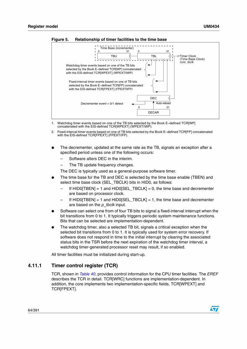
Register model UM0434
64/391
Figure 5. Relationship of timer facilities to the time base
1. Watchdog timer events based on one of the TB bits selected by the Book E–defined TCR[WP] concatenated with the EIS-defined TCR[WPEXT] (WPEXT||WP).
2. Fixed-interval timer events based on one of TB bits selected by the Book E–defined TCR[FP] concatenated with the EIS-defined TCR[FPEXT] (FPEXT||FP).
● The decrementer, updated at the same rate as the TB, signals an exception after a specified period unless one of the following occurs:
– Software alters DEC in the interim.
– The TB update frequency changes.
The DEC is typically used as a general-purpose software timer.
● The time base for the TB and DEC is selected by the time base enable (TBEN) and select time base clock (SEL_TBCLK) bits in HID0, as follows:
– If HID0[TBEN] = 1 and HID0[SEL_TBCLK] = 0, the time base and decrementer are based on processor clock.
– If HID0[TBEN] = 1 and HID0[SEL_TBCLK] = 1, the time base and decrementer are based on the p_tbclk input.
● Software can select one from of four TB bits to signal a fixed-interval interrupt when the bit transitions from 0 to 1. It typically triggers periodic system maintenance functions. Bits that can be selected are implementation-dependent.
● The watchdog timer, also a selected TB bit, signals a critical exception when the selected bit transitions from 0 to 1. It is typically used for system error recovery. If software does not respond in time to the initial interrupt by clearing the associated status bits in the TSR before the next expiration of the watchdog timer interval, a watchdog timer-generated processor reset may result, if so enabled.
All timer facilities must be initialized during start-up.
4.11.1 Timer control register (TCR)
TCR, shown in Table 40, provides control information for the CPU timer facilities. The EREF describes the TCR in detail. TCR[WRC] functions are implementation-dependent. In addition, the core implements two implementation-specific fields, TCR[WPEXT] and TCR[FPEXT].
Timer Clock
Time Base (incrementer)
Decrementer event = 0/1 detect31
DECAR
0
Auto-reload
310
TBL
310
TBU
Watchdog timer events based on one of the TB bitsselected by the Book E–defined TCR[WP] concatenatedwith the EIS-defined TCR[WPEXT] (WPEXTIIWP)
Fixed-interval timer events based on one of TB bitsselected by the Book E–defined TCR[FP] concatenatedwith the EIS-defined TCR[FPEXT] (FPEXTIIFP)
DEC
(Time Base Clock)core_tbclk

UM0434 Register model
65/391
The TCR fields are described in Table 41.
Table 40. Timer control register (TCR)
32333435 36 37 3839 40 41 4243 46 47 50 51 63
Field WP WRCWIE DIE FP FIE ARE — WPEXT FPEXT —
Reset All zeros
R/W R/W
SPR SPR 340
Table 41. TCR field descriptions
Bits Name Description
32–33 WP
Watchdog timer period, When concatenated with WPEXT, specifies one of 64 bit locations of the time base used to signal a watchdog timer exception on a transition from 0 to 1.
TCR[WPEXT]||TCR[WP] == 000000 selects TBU[32] (msb of TBU).
TCR[WPEXT]||TCR[WP] == 111111 selects TBL[63] (lsb of TBL).
34–35 WRC
Watchdog timer reset control. Software can set WRC but cannot clear it except by a software-induced reset. After WRC is written to a non-zero value, software can no longer alter it.
00 No watchdog timer reset can occur.
01 Force processor checkstop on second time-out of the watchdog timer.10 Assert processor reset output (p_resetout_b) on second time-out of watchdog timer.
11 Reserved.
36 WIE
Watchdog timer interrupt enable.
0 Watchdog timer interrupts disabled.
1 Watchdog timer interrupts enabled.
37 DIE
Decrementer interrupt enable.
0 Decrementer interrupts disabled.1 Decrementer interrupts enabled.
38–39 FP
Fixed-interval timer period. When concatenated with FPEXT, specifies one of 64 bit locations of the time base to signal a fixed-interval timer exception on a transition from 0 to 1.
TCR[FPEXT]||TCR[FP] == 000000 selects TBU[32] (msb of TBU).TCRFP[EXT]||TCR[FP] == 111111 selects TBL[63] (lsb of TBL).
40 FIEFixed-interval interrupt enable.0 Fixed-interval interrupts disabled.
1 Fixed-interval interrupts enabled.
41 ARE
Auto-reload enable. Controls whether the value in DECAR is reloaded into DEC when the DEC value reaches 0000_0001.0 Auto-reload disabled.
1 Auto-reload enabled.
42 — Reserved, should be cleared.
43–46 WPEXTWatchdog timer period extension (see above description for WP). WPEXT | WP select one of the 64 TB bits used to signal a watchdog timer exception.
Register model UM0434
66/391
4.11.2 Timer status register (TSR)
TSR, shown in Table 42, provides status information for the CPU timer facilities. EREF describes the TSR in detail. TSR[WRS] is defined as implementation-dependent.
Register fields designated as write-1-to-clear are cleared only by writing ones to them. Writing zeros to them has no effect.
The TSR fields are described in Table 43.
47–50 FPEXTFixed-interval timer period extension (see description for FP). FPEXT | FP select one of the 64 TB bits used to signal a fixed-interval timer exception.
51–63 — Reserved, should be cleared.
Table 41. TCR field descriptions (continued)
Bits Name Description
Table 42. Timer status register (TSR)
32 33 34 35 36 37 38 63
Field ENW WIS WRS DIS FIS —
Reset 0b(00||WRS)_0000_0000_0000_0000_0000_0000_0000
R/W Read/Clear
SPR SPR 336
Table 43. Timer status register field descriptions
Bits Name Description
32 ENW
Enable next watchdog time. When a watchdog timer time-out occurs while WIS = 0 and the next watchdog time-out is enabled (ENW = 1), a watchdog timer exception is generated and logged by setting WIS. This is a watchdog timer first time out. A watchdog timer interrupt occurs if enabled by TCR[WIE] and MSR[CE]. To avoid another watchdog timer interrupt when MSR[CE] is reenabled (assuming TCR[WIE] is not cleared instead), the interrupt handler must reset TSR[WIS] by executing an mtspr, setting WIS and any other bits to be cleared and a 0 in all other bits. The data written to the TSR is not direct data, but is a mask. A 1 causes the bit to be cleared; a 0 has no effect.
0 Action on next watchdog timer time-out is to set TSR[ENW].
1 Action on next watchdog timer time-out is governed by TSR[WIS].
33 WIS
Watchdog timer interrupt status. See the ENW description for details on how WIS is used.
0 No watchdog timer event.
1 A watchdog timer event. When MSR[CE] = 1 and TCR[WIE] = 1, a watchdog timer interrupt is taken.
34–35 WRS
Watchdog timer reset status.
00 No second time-out of watchdog timer.
01 Force processor checkstop on second time-out of watchdog timer.
10 Assert processor reset output (p_resetout_b) on second time-out of watchdog timer.
11 Reserved.

UM0434 Register model
67/391
Note: The TSR can be read using mfspr rD,TSR. The TSR cannot be directly written. Instead, TSR bits corresponding to 1 bits in GPR(rS) can be cleared using mtspr TSR,rS.
4.11.3 Time base (TBU and TBL)
The time base (TB), seen in Table 44, is composed of two 32-bit registers, the time base upper (TBU) concatenated on the right with the time base lower (TBL). The time base registers provide timing functions for the system and are enabled by setting HID0[TBEN]. The decrementer (DEC) updates at the same frequency, which is selected in HID0[SEL_TBCLK]. TB is a volatile resource and must be initialized during start-up. For details, see Section 4.11: Timer registers on page 63.”
The TB is interpreted as a 64-bit unsigned integer that is periodically incremented. Each increment adds 1 to the least-significant bit. The frequency at which the integer is updated is implementation-dependent.
TBL increments until its value becomes 0xFFFF_FFFF (232 – 1). At the next increment, its value becomes 0x0000_0000 and TBU is incremented. This process continues until the TBU value becomes 0xFFFF_FFFF and the TBL value becomes 0xFFFF_FFFF (TB is interpreted as 0xFFFF_FFFF_FFFF_FFFF (264 – 1)). At the next increment, the TBU value becomes 0x0000_0000 and the TBL value becomes 0x0000_0000. There is no interrupt (or any other indication).
The period depends on the driving frequency. For example, if TB is driven by 100 MHz divided by 32, the TB period is as follows:
36 DIS
Decrementer interrupt status.
0 No decrementer event.
1 Decrementer event. When MSR[EE] = TCR[DIE] = 1, a decrementer interrupt is taken.
37 FIS
Fixed-interval timer interrupt status.
0 No fixed-interval timer event.
1 Fixed-interval timer event. When MSR[EE] = 1 and TCR[FIE] = 1, a fixed-interval timer interrupt is taken.
38–63 — Reserved, should be cleared.
Table 43. Timer status register field descriptions (continued)
Bits Name Description
Table 44. Time base upper/lower registers (TBU/TBL)
32 63 32 63
Field TBU TBL
ResetUndefined on m_por assertion, unchanged on
p_reset_b assertionUndefined on m_por assertion, unchanged on
p_reset_b assertion
R/W User read/Supervisor write User read/Supervisor write
SPR 269 Read/285 Write 268 Read/284 Write

Register model UM0434
68/391
The TB is implemented to satisfy the following requirements:
● Loading a GPR from the TB has no effect on the accuracy of the TB.
● Storing a GPR to the TB replaces the value in the TB with the value in the GPR.
Book E does not specify a relationship between the TB update frequency and other frequencies, such as the CPU clock or bus clock. The TB update frequency does not have to be constant. One of the following is required to ensure that system software can keep time of day and operate interval timers:
● The system provides an (implementation-dependent) interrupt to software when the update frequency of the TB changes and a way to determine the current update frequency.
● The update frequency of the TB is under the control of system software.
Note: Disabling the TB or making reading the time base privileged prevents the TB from being used to implement a covert channel in a secure system. If the operating system initializes the TB on power-on to some reasonable value and the update frequency of the TB is constant, the TB can be used as a source of values that increase at a constant rate, such as for time stamps in trace entries.Even if the update frequency is not constant, values read from the TB are monotonically increasing (except when the TB wraps from 264 – 1 to 0). If a trace entry is recorded each time the update frequency changes, the sequence of TB values can be post-processed to become actual time values.Successive readings of the TB may return identical values.
The TB is useful for timing reasonably short sequences of code (a few hundred instructions) and for low-overhead time stamps for tracing.
4.11.4 Decrementer register
DEC, shown in Table 45, is a decrementing counter that is enabled by setting HID0[TBEN]. The decrementer and time base update at the same frequency, which is selected in HID0[SEL_TBCLK]. It provides way to signal a decrementer interrupt after a specified period unless one of the following occurs:
● Software alters DEC in the interim.
● The TB update frequency changes.
DEC is typically used as a general-purpose software timer. The decrementer auto-reload register (DECAR) automatically reloads a programmed value into DEC.
TTB 264 32
100 MHz------------------------× 5.90 10
12× ondssec= = (approximately 187,000 years)
Table 45. Decrementer register (DEC)
32 63
Field Decrementer value
Reset Undefined on m_por assertion, unchanged on p_reset_b assertion
R/W R/W
SPR SPR 22

UM0434 Register model
69/391
4.11.5 Decrementer auto-reload register (DECAR)
If the auto-reload function is enabled (TCR[ARE] = 1), the auto-reload value in DECAR, shown in Table 46, is written to DEC when DEC decrements from 0x0000_0001 to 0x0000_0000. Writing DEC with zeros by using an mtspr does not automatically generate a decrementer interrupt.
4.12 Debug registersThis section describes software-accessible debug registers for use by special debug tools and debug software, not by general application code. Software access to these registers is conditioned by the external debug mode control bit (DBCR0[EDM]), which can be set by the hardware debug port. If DBCR0[EDM] is set, software is prevented from modifying debug register values. Execution of an mtspr instruction targeting a debug register does not cause modifications to occur. In addition, since the external debugger hardware may be manipulating debug register values, the state of these registers is not guaranteed to be consistent if read by software with an mfspr instruction other than DBCR0[EDM].
4.12.1 Debug address and value registers
Instruction address compare registers IAC1–IAC4 hold instruction addresses for comparison. In addition, IAC2 and IAC4 hold mask information for IAC1 and IAC3, respectively, when address bit match compare modes are selected.
Note: During instruction address comparisons, the low-order two address bits of the instruction address and the corresponding IAC register are ignored.
Data address compare registers DAC1 and DAC2 hold data access addresses for comparison. In addition, DAC2 holds mask information for DAC1 when address bit match compare mode is selected.
Instruction address compare registers (IAC1–IAC4)
IAC1–IAC4, shown in Table 47, hold instruction addresses for comparison.
Table 46. Decrementer auto-reload register (DECAR)
32 63
Field Decrementer auto-reload value
Reset Undefined on m_por assertion, unchanged on p_reset_b assertion
R/W R/W
SPR SPR 54
Table 47. Instruction address compare registers (IAC1–IAC4)
32 616263
Field Instruction address —
Reset All zeros
R/W R/W
SPR SPR 312 (IAC1); SPR 313 (IAC2); SPR 314 (IAC3); SPR 315 (IAC4)

Register model UM0434
70/391
A debug event can be enabled when there is an attempt to execute an instruction from an address in one of the following contexts:
● In an IAC
● Inside or outside a range specified by IAC1 and IAC2
● Inside or outside a range specified by IAC3 and IAC4
● To blocks of addresses specified by the combination of the IAC1 and IAC2
● To blocks of addresses specified by the combination of the IAC3 and IAC4.
Because all instruction addresses must be word-aligned, the two low-order bits of the IACs are reserved and do not participate in the comparison with the instruction address.
Data address compare registers (DAC1–DAC2)
The data address compare 1 register (DAC1) and data address compare 2 register (DAC2), shown in Table 48, are each 32 bits. A debug event can be enabled by loads, stores, or cache operations to an address specified in either DAC1 or DAC2, inside or outside a range specified by the DAC1 and DAC2, or blocks of addresses specified by the combination of the DAC1 and DAC2.
The contents of DAC1 or DAC2 are compared to the address generated by a data access instruction.
4.12.2 Debug counter register (DBCNT)
The debug counter register (DBCNT) contains two 16-bit counters (CNT1 and CNT2) that can be configured to operate independently or concatenated into a single 32-bit counter. Each counter can be configured to count down (decrement) when one or more count-enabled events occur. The counters operate regardless of whether counters are enabled to generate debug exceptions. When a count value reaches zero, a debug count event is signaled and a debug event can be generated (if enabled). Upon reaching zero, the counter is frozen. A debug counter signals an event on the transition from a value of one to a final value of zero. Loading a value of zero into the counter prevents the counter from counting. The debug counter is configured by the contents of DBCR3. DBCNT is shown in Table 49.
Table 48. Data address compare registers (DAC1–DAC2)
32 63
Field Data address
Reset All zeros
R/W R/W
SPR SPR 316 (DAC1); SPR 317 (DAC2)
Table 49. DBCNT register
32 47 48 63
Field CNT1 CNT2
Reset Undefined on m_por assertion, unchanged on p_reset_b assertion
R/W R/W
SPR SPR 562

UM0434 Register model
71/391
Refer to Section : Debug control register 3 (DBCR3) on page 77,” for details on updates to the DBCNT register. There are restrictions on how the DBCNT and DBCR3 register are modified when one or more counters are enabled.
4.12.3 Debug control and status registers (DBCR0–DBCR3)
DBCR0–DBCR3 enable debug events, reset the processor, control timer operation during debug events and set the debug mode of the processor. The debug status register (DBSR) records debug exceptions while internal or external debug mode is enabled.
To ensure that any alterations enabling/disabling debug events are effective, the e200z3 requires that a context synchronizing instruction follow an mtspr that updates a DBCR or DBSR. The context synchronizing instruction may or may not be affected by the alteration. Typically, an isync is used to create a synchronization boundary beyond which it can be guaranteed that the newly written control values are in effect. For watchpoint generation and counter operation, configuration settings in DBCR1–DBCR3 are used, even though the corresponding events can be disabled (via DBCR0) from setting DBSR flags.
Debug Control Register 0 (DBCR0)
DBCR0 is used to enable debug modes and controls which debug events are allowed to set DBSR flags. The e200z3 adds bits to this register, as shown in Table 50.
Table 51 provides field definitions for DBCR0.
Table 50. DBCR0 Register
32 33 3435 36 37 38 39 40 41 42 43 44 45 46 47
Field EDM IDM RST ICMP BRT IRPT TRAP IAC1 IAC2 IAC3 IAC4 DAC1 DAC2
Reset All zeros(1)
1. DBCR0[EDM] is affected by j_trst_b or m_por assertion, and while in the test_logic_reset state, but not by p_reset_b. All other bits are reset by processor reset p_reset_b as well as by m_por.
R/W R/W
48 49 52 53 54 55 56 57 58 59 62 63
RET — DEVT1 DEVT2 DCNT1 DCNT2 CIRPT CRET VLES — FT
Reset All zeros 1
R/W R/W
SPR SPR 308
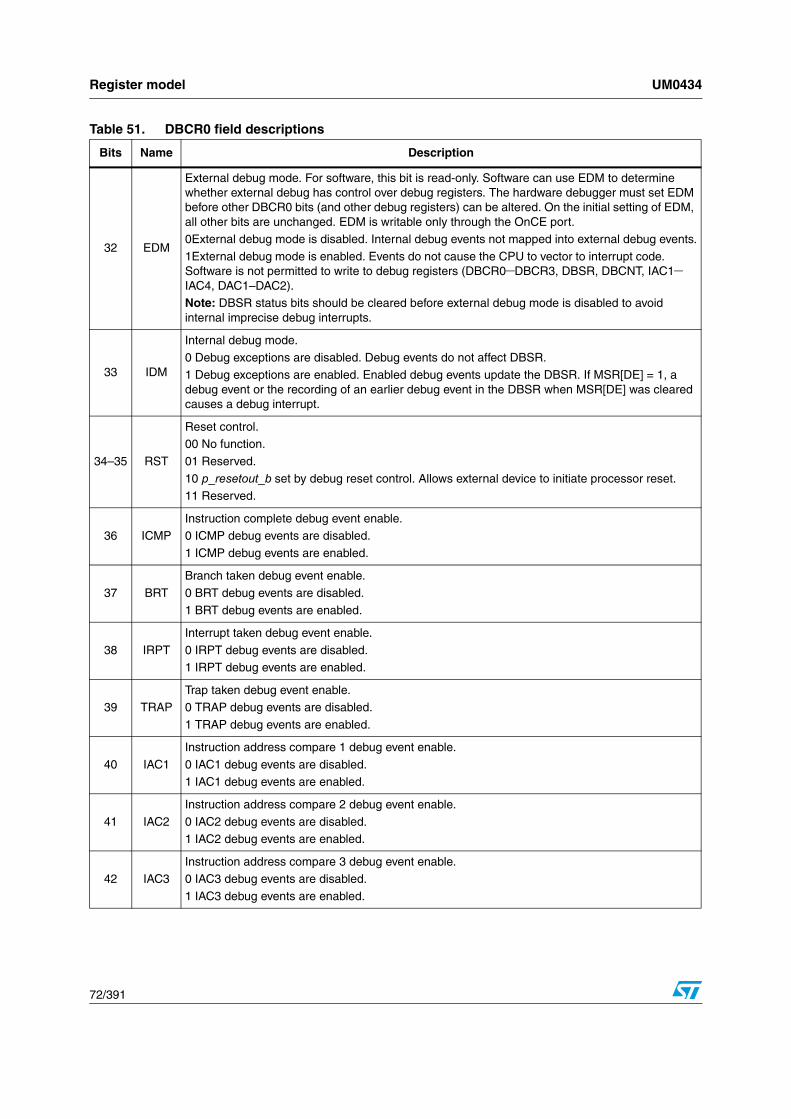
Register model UM0434
72/391
Table 51. DBCR0 field descriptions
Bits Name Description
32 EDM
External debug mode. For software, this bit is read-only. Software can use EDM to determine whether external debug has control over debug registers. The hardware debugger must set EDM before other DBCR0 bits (and other debug registers) can be altered. On the initial setting of EDM, all other bits are unchanged. EDM is writable only through the OnCE port.0External debug mode is disabled. Internal debug events not mapped into external debug events.
1External debug mode is enabled. Events do not cause the CPU to vector to interrupt code. Software is not permitted to write to debug registers (DBCR0–DBCR3, DBSR, DBCNT, IAC1–IAC4, DAC1–DAC2).Note: DBSR status bits should be cleared before external debug mode is disabled to avoid internal imprecise debug interrupts.
33 IDM
Internal debug mode.
0 Debug exceptions are disabled. Debug events do not affect DBSR.1 Debug exceptions are enabled. Enabled debug events update the DBSR. If MSR[DE] = 1, a debug event or the recording of an earlier debug event in the DBSR when MSR[DE] was cleared causes a debug interrupt.
34–35 RST
Reset control.00 No function.
01 Reserved.
10 p_resetout_b set by debug reset control. Allows external device to initiate processor reset.11 Reserved.
36 ICMPInstruction complete debug event enable.0 ICMP debug events are disabled.
1 ICMP debug events are enabled.
37 BRT
Branch taken debug event enable.
0 BRT debug events are disabled.
1 BRT debug events are enabled.
38 IRPT
Interrupt taken debug event enable.
0 IRPT debug events are disabled.1 IRPT debug events are enabled.
39 TRAPTrap taken debug event enable.0 TRAP debug events are disabled.
1 TRAP debug events are enabled.
40 IAC1
Instruction address compare 1 debug event enable.
0 IAC1 debug events are disabled.
1 IAC1 debug events are enabled.
41 IAC2
Instruction address compare 2 debug event enable.
0 IAC2 debug events are disabled.1 IAC2 debug events are enabled.
42 IAC3Instruction address compare 3 debug event enable.0 IAC3 debug events are disabled.
1 IAC3 debug events are enabled.

UM0434 Register model
73/391
43 IAC4
Instruction address compare 4 debug event enable.
0 IAC4 debug events are disabled.
1 IAC4 debug events are enabled.
44–45 DAC1
Data address compare 1 debug event enable
00 DAC1 debug events are disabled.01 DAC1 debug events are enabled only for store-type data storage accesses.
10 DAC1 debug events are enabled only for load-type data storage accesses.
11 DAC1 debug events are enabled for load-type or store-type data storage accesses.
46–47 DAC2
Data address compare 2 debug event enable.
00 DAC2 debug events are disabled.01 DAC2 debug events are enabled only for store-type data storage accesses.
10 DAC2 debug events are enabled only for load-type data storage accesses.
11 DAC2 debug events are enabled for load-type or store-type data storage accesses.
48 RET
Return debug event enable.
0 RET debug events are disabled.
1 RET debug events are enabled.
49–52 — Reserved.
53 DEVT1
External debug event 1 enable.
0 DEVT1 debug events are disabled.
1 DEVT1 debug events are enabled.
54 DEVT2
External debug event 2 enable.
0 DEVT2 debug events are disabled.1 DEVT2 debug events are enabled.
55 DCNT1Debug counter 1 debug event enable.0 counter 1 debug events are disabled.
1 counter 1 debug events are enabled.
56 DCNT2
Debug counter 2 debug event enable.
0 counter 2 debug events are disabled.
1 counter 2 debug events are enabled.
57 CIRPT
Critical interrupt taken debug event enable.
0 CIRPT debug events are disabled.1 CIRPT debug events are enabled.
58 CRETCritical return debug event enable.0 CRET debug events are disabled.
1 CRET debug events are enabled.
59 VLESVLE status, Set if an ICMP, BRT, TRAP, RET, CRET, IAC, or DAC debug event occurred on a VLE instruction. Undefined for IRPT, CIRPT, DEVT[1,2], DCNT[1,2], and UDE events.
60–62 — Reserved.
63 FT
Freeze timers on debug event.
0 Timebase timers are unaffected by set DBSR bits.
1 Disable clocking of timebase timers if any DBSR bit is set (except MRR or CNT1TRG).
Table 51. DBCR0 field descriptions (continued)
Bits Name Description

Register model UM0434
74/391
Debug control register 1 (DBCR1)
DBCR1, shown in Table 52, is used to configure instruction address compare operation.
Table 53 describes debug control register 1 fields.
Table 52. Debug control register 1 (DBCR1)
32 33 34 35 36 37 38 39 40 41 42 47 48 49 50 51 52 53 54 55 56 57 58 63
Field IAC1USIAC1ERIAC2USIAC2ERIAC12M — IAC3USIAC3ERIAC4USIAC4ERIAC34M —
Reset All zeros
R/W R/W
SPR SPR 309
Table 53. DBCR1 field descriptions
Bits Name Description
32–33 IAC1US
Instruction address compare 1 user/supervisor mode.00 AC1 debug events are not affected by MSR[PR].
01 Reserved.
10 AC1 debug events can occur only if MSR[PR] = 0 (supervisor mode).11 AC1 debug events can occur only if MSR[PR] = 1 (user mode).
34–35 IAC1ER
Instruction address compare 1 effective/real mode.00 AC1 debug events are based on effective address.
01 Unimplemented in the e200z3 (Book E real address compare), no match can occur.
10 AC1 debug events are based on effective address and can occur only if MSR[IS] = 0.11 AC1 debug events are based on effective address and can occur only if MSR[IS] = 1.
36–37 IAC2US
Instruction address compare 2 user/supervisor mode.00 AC2 debug events are not affected by MSR[PR].
01 Reserved.
10 AC2 debug events can occur only if MSR[PR] = 0 (supervisor mode).11 AC2 debug events can occur only if MSR[PR] = 1 (user mode).
38–39 IAC2ER
Instruction address compare 2 effective/real mode.00 AC2 debug events are based on effective address.
01 Unimplemented in the e200z3 (Book E real address compare), no match can occur.
10 AC2 debug events are based on effective address and can occur only if MSR[IS] = 0.11 AC2 debug events are based on effective address and can occur only if MSR[IS] = 1.

UM0434 Register model
75/391
40–41 IAC12M
Instruction address compare 1/2 mode.
00 Exact address compare. IAC1 debug events can occur only if the address of the instruction fetch is equal to the value specified in IAC1. IAC2 debug events can occur only if the address of the instruction fetch is equal to the value specified in IAC2.01 Address bit match. IAC1 debug events can occur only if the address of the instruction fetch ANDed with the contents of IAC2 is equal to the contents of IAC1, also ANDed with the contents of IAC2. IAC2 debug events do not occur. IAC1US and IAC1ER settings are used.
10 Inclusive address range compare. IAC1 debug events can occur only if the address of the instruction fetch is greater than or equal to the value specified in IAC1 and less than the value specified in IAC2. IAC2 debug events do not occur. IAC1US and IAC1ER settings are used.
11 Exclusive address range compare. IAC1 debug events can occur only if the address of the instruction fetch is less than the value specified in IAC1 or is greater than or equal to the value specified in IAC2. IAC2 debug events do not occur. IAC1US and IAC1ER settings are used.
42–47 — Reserved
48–49 IAC3US
Instruction address compare 3 user/supervisor mode.00 AC3 debug events are not affected by MSR[PR].
01 Reserved.
10 AC3 debug events can occur only if MSR[PR] = 0 (supervisor mode).11 AC3 debug events can occur only if MSR[PR] = 1 (user mode).
50–51 IAC3ER
Instruction address compare 3 effective/real mode.00 AC3 debug events are based on effective address.
01 Unimplemented in the e200z3 (Book E real address compare), no match can occur.
10 AC3 debug events are based on effective address and can occur only if MSR[IS] = 0.11 AC3 debug events are based on effective address and can occur only if MSR[IS] = 1.
52–53 IAC4US
Instruction address compare 4 user/supervisor mode.00 AC4 debug events are not affected by MSR[PR].
01 Reserved.
10 IAC4 debug events can occur only if MSR[PR] = 0 (supervisor mode).11 IAC4 debug events can occur only if MSR[PR] = 1 (user mode).
54–55 IAC4ER
Instruction address compare 4effective/real mode.00 AC4 debug events are based on effective address.
01 Unimplemented in the e200z3 (Book E real address compare), no match can occur.
10 IAC4 debug events are based on effective address and can occur only if MSR[IS] = 0.11 IAC4 debug events are based on effective address and can occur only if MSR[IS] = 1.
Table 53. DBCR1 field descriptions (continued)
Bits Name Description

Register model UM0434
76/391
Debug control register 2 (DBCR2)
DBCR2, shown below is used to configure data address compare operations.
Table 54 describes DBCR2 fields.
56–57 IAC34M
Instruction address compare 3/4 mode.
00 Exact address compare. IAC3 debug events can occur only if the address of the instruction fetch is equal to the value specified in IAC3. IAC4 debug events can occur only if the address of the instruction fetch is equal to the value specified in IAC4.01 Address bit match. IAC3 debug events can occur only if the address of the instruction fetch ANDed with the contents of IAC4 is equal to the contents of IAC3, also ANDed with the contents of IAC4. IAC4 debug events do not occur. IAC3US and IAC3ER settings are used.
10 Inclusive address range compare. IAC3 debug events can occur only if the address of the instruction fetch is greater than or equal to the value specified in IAC3 and less than the value specified in IAC4. IAC4 debug events do not occur. IAC3US and IAC3ER settings are used.
11 Exclusive address range compare. IAC3 debug events can occur only if the address of the instruction fetch is less than the value specified in IAC3 or is greater than or equal to the value specified in IAC4. IAC4 debug events do not occur. IAC3US and IAC3ER settings are used.
58–63 — Reserved
Table 53. DBCR1 field descriptions (continued)
Bits Name Description
32 33 34 35 36 37 38 39 40 41 42 43 44 63
Field DAC1US DAC1ER DAC2US DAC2ER DAC12M DAC1LNK DAC2LNK —
Reset All zeros
R/W R/W
SPR SPR 310
Table 54. DBCR2 field descriptions
Bits Name Description
32–33 DAC1US
Data address compare 1 user/supervisor mode.
00 DAC1 debug events are not affected by MSR[PR].
01 Reserved.10 DAC1 debug events can occur only if MSR[PR] = 0 (supervisor mode).
11 DAC1 debug events can occur only if MSR[PR] = 1 (User mode).
34–35 DAC1ER
Data address compare 1 effective/real mode.
00 DAC1 debug events are based on effective address.
01 Unimplemented in the e200z3 (Book E real address compare), no match can occur.10 DAC1 debug events are based on effective address and can occur only if MSR[DS] = 0.
11 DAC1 debug events are based on effective address and can occur only if MSR[DS] = 1.
36–37 DAC2US
Data Address compare 2 user/supervisor mode.
00 DAC2 debug events are not affected by MSR[PR].
01 Reserved10 DAC2 debug events can occur only if MSR[PR] = 0 (supervisor mode).
11 DAC2 debug events can occur only if MSR[PR] = 1 (user mode).

UM0434 Register model
77/391
Debug control register 3 (DBCR3)
DBCR3, shown in Table 55, is an e200z3 implementation-specific register to enable and configure the debug counter and debug counter events. For counter operation, the specific debug events that cause counters to decrement are specified in DBCR3.
Note: Corresponding events do not need to be (and probably should not be) enabled in DBCR0.
The IAC1–IAC4 and DAC1–DAC2 control fields in DBCR0 are ignored for counter operations and the control fields in DBCR3 determine when counting is enabled. DBCR1 and DBCR2 control fields are also used to determine the configuration of IAC1–IAC4 and DAC1–DAC2 operations for counting, even though the setting of bits in DBSR by corresponding events can be disabled via DBCR0. Multiple count-enabled events that occur during execution of an instruction typically cause only one decrement of a counter. For example, if more than one IAC or DAC register hits and is enabled for counting, only one count can occur per counter. During execution of lmw and stmw instructions, multiple DACn hits can occur. If the instruction is not interrupted before completion, a single decrement of a counter occurs.
38–39 DAC2ER
Data address compare 2 effective/real mode.
00 DAC2 debug events are based on effective address.
01 Unimplemented in the e200z3 (Book E real address compare), no match can occur.10 DAC2 debug events are based on effective address and can occur only if MSR[DS] = 0.
11 DAC2 debug events are based on effective address and can occur only if MSR[DS] = 1.
40–41 DAC12M
Data address compare 1/2 mode.
00 Exact address compare. DAC1 debug events can occur only if the address of the data access is equal to the value specified in DAC1. DAC2 debug events can occur only if the address of the data access is equal to the value specified in DAC2.01 Address bit match. DAC1 debug events can occur only if the address of the data access ANDed with the contents of DAC2 is equal to the contents of DAC1, also ANDed with the contents of DAC2. DAC2 debug events do not occur. DAC1US and DAC1ER settings are used.
10 Inclusive address range compare. DAC1 debug events can occur only if the address of the data access is greater than or equal to the value specified in DAC1 and less than the value specified in DAC2. DAC2 debug events do not occur. DAC1US and DAC1ER settings are used.11 Exclusive address range compare. DAC1 debug events can occur only if the address of the data access is less than the value specified in DAC1 or is greater than or equal to the value specified in DAC2. DAC2 debug events do not occur. DAC1US and DAC1ER settings are used.
42 DAC1LNK
Data address compare 1 linked.
0 No effect.
1 DAC1 debug events are linked to IAC1 debug events. IAC1 debug events do not affect DBSR.When linked to IAC1, DAC1 debug events are conditioned based on whether the instruction also generated an IAC1 debug event.
43 DAC2LNK
Data address compare 2 linked
0 No effect.1DAC 2 debug events are linked to IAC3 debug events. IAC3 debug events do not affect DBSR.
When linked to IAC3, DAC2 debug events are conditioned based on whether the instruction also generated an IAC3 debug event. DAC2 can only be linked if DAC12M specifies exact address compare because DAC2 debug events are not generated in the other compare modes.
44–63 — Reserved for data value compare control (not supported by the e200z3).
Table 54. DBCR2 field descriptions (continued)
Bits Name Description

Register model UM0434
78/391
Note: If the counters operate independently, both may count for the same instruction.
The debug counter register (DBCNT) is configured by DBCR3[CONFIG] to operate either as separate 16-bit counter 1 and counter 2 or as a combined 32-bit counter (using control bits in DBCR3 for counter 1). Counters are enabled when any of their respective count enable event control bits are set and either DBCR0 or DBCR0[EDM] is set. Counter 1 can be configured to count down on a number of different debug events. Counter 2 is also configurable to count down on instruction complete, instruction or data address compare events, and external events.
Special capability is provided for counter 1 to be triggered to begin counting down by a subset of events (IAC1, IAC3, DAC1R, DAC1W, DEVT1, DEVT2, and counter 2). When one or more of the counter 1 trigger bits is set (IAC1T1, IAC3T1, DAC1RT1, DAC1WT1, DEVT1T1, DEVT2T1, CNT2T1), counter 1 is frozen until at least one of the triggering events occurs and is then enabled to begin operation. Triggering status for counter 1 is provided in the debug status register. Triggering mode is enabled by an mtspr DBCR3 which sets one or more of the trigger enable bits and also enables counter 1. The trigger can be re-armed by clearing the DBSR[CNT1TRG] status bit.
Most combinations of enables do not make sense and should be avoided. For example, if DBCR3[ICMP] is set for counter 1, no other count enable should be set for counter 1. Conversely, multiple instruction address compare count enables are allowed to be set and can be useful.
Due to instruction pipelining issues and other constraints, most combinations of events are not supported for event counting. Only the following combinations are for use; other combinations are not supported:
● Any combination of IAC[1–4]
● Any combination of DAC[1–2] including linking
● Any combination of DEVT[1–2]
● Any combination of IRPT and RET
Limited support is provided for any combination of IAC[1–4] with DAC[1–2] (linked or unlinked).
Due to pipelining and detection of IAC events early in the pipeline and DAC events late in the pipeline, no guarantee is made on the exact instruction boundary that a debug exception is generated when IAC and DAC events are combined for counting. This also applies when counter 1 is triggered by counter 2, and a combination of IAC and DAC events is enabled for the counters, even if only one of these types is enabled for a particular counter. In general, when an IAC event logically follows a DAC event within several instructions, it cannot be recognized immediately because the DAC event may not be generated in the pipeline at the time the IAC appears. Thus, the counter may not decrement to zero for the IAC event until after the instruction with the IAC (and perhaps several additional instructions) proceeds down the execution pipeline. The instruction boundary where the debug exception is actually generated typically follows the IAC by up to several instructions.
Note that the counters operate regardless of whether counters are enabled to generate debug exceptions.
If counter 2 is used to trigger counter 1, counter 2 events should not normally be enabled in DBCR0 and are not blocked.
Note: Multiple IAC or DAC events are not counted during an lmw or stmw instruction, and no count occurs if either is interrupted by a critical input or external input interrupt before completion.

UM0434 Register model
79/391
Table 56 provides field definitions for DBCR3
Table 55. DBCR3 register
32 33 34 35 36 37 38 39
Field DEVT1C1 DEVT2C1 ICMPC1 IAC1C1 IAC2C1 IAC3C1 IAC4C1 DAC1RC1
Reset All zeros
R/W R/W
40 41 42 43 44 45 46 47
Field DAC1WC1 DAC2RC1 DAC2WC1 IRPTC1 RETC1 DEVT1C2 DEVT2C2 ICMPC2
Reset All zeros
R/W R/W
48 49 50 51 52 53 54 55
IAC1C2 IAC2C2 IAC3C2 IAC4C2 DAC1RC2 DAC1WC2 DAC2RC2 DAC2WC2
Reset All zeros
R/W R/W
56 57 58 59 60 61 62 63
DEVT1T1 DEVT2T1 IAC1T1 IAC3T1 DAC1RT1 DAC1WT1 CNT2T1 CONFIG
Reset All zeros
R/W R/W
SPR SPR 561
Table 56. DBCR3 field descriptions
Bits Name Description
32 DEVT1C1External debug event 1 count 1 enable.0 Counting DEVT1 debug events by counter 1 is disabled.
1 Counting DEVT1 debug events by counter 1 is enabled.
33 DEVT2C1
External debug event 2 count 1 enable.
0 Counting DEVT2 debug events by counter 1 is disabled.
1 Counting DEVT2 debug events by counter 1 is enabled.
34 ICMPC1
Instruction complete debug event count 1 enable.
0 Counting ICMP debug events by counter 1 is disabled.1 Counting ICMP debug events by counter 1 is enabled.
ICMP events are masked by MSR[DE] = 0 when operating in internal debug mode.
35 IAC1C1
Instruction address compare 1 debug event count 1 enable.
0 Counting IAC1 debug events by counter 1 is disabled.
1 Counting IAC1 debug events by counter 1 is enabled.
36 IAC2C1
Instruction address compare2 debug event count 1 enable.
0 Counting IAC2 debug events by counter 1 is disabled.1 Counting IAC2 debug events by counter 1 is enabled.

Register model UM0434
80/391
37 IAC3C1
Instruction address compare 3 debug event count 1 enable.
0 Counting IAC3 debug events by counter 1 is disabled.
1 Counting IAC3 debug events by counter 1 is enabled.
38 IAC4C1
Instruction address compare 4 debug event count 1 enable.
0 Counting IAC4 debug events by counter 1 is disabled.1 Counting IAC4 debug events by counter 1 is enabled.
39 DAC1RC1Data address compare 1 read debug event count 1 enable(1).0 Counting DAC1R debug events by counter 1 is disabled.
1 Counting DAC1R debug events by counter 1 is enabled.
40 DAC1WC1
Data address compare 1 write debug event count 1 enable (1).
0 Counting DAC1W debug events by counter 1 is disabled.
1 Counting DAC1W debug events by counter 1 is enabled.
41 DAC2RC1
Data address compare 2 read debug event count 1 enable (1).
0 Counting DAC2R debug events by counter 1 is disabled.
1 Counting DAC2R debug events by counter 1 is enabled.
42 DAC2WC1
Data address compare 2 write debug event count 1 enable (1).
0 Counting DAC2W debug events by counter 1 is disabled.1 Counting DAC2W debug events by counter 1 is enabled.
43 IRPTC1Interrupt taken debug event count 1 enable.0 Counting IRPT debug events by counter 1 is disabled.
1 Counting IRPT debug events by counter 1 is enabled.
44 RETC1
Return debug event count 1 enable.
0 Counting RET debug events by counter 1 is disabled.
1 Counting RET debug events by counter 1 is enabled.
45 DEVT1C2
External debug event 1 count 2 enable.
0 Counting DEVT1 debug events by counter 2 is disabled.1 Counting DEVT1 debug events by counter 2 is enabled.
46 DEVT2C2External debug event 2 count 2 enable.0 Counting DEVT2 debug events by counter 2 is disabled.
1 Counting DEVT2 debug events by counter 2 is enabled.
47 ICMPC2
Instruction complete debug event count 2 enable.
0 Counting ICMP debug events by counter 2 is disabled.
1 Counting ICMP debug events by counter 2 is enabled.ICMP events are masked by MSR[DE] = 0 when operating in internal debug mode.
48 IAC1C2Instruction address compare 1 debug event count 2 enable.0 Counting IAC1 debug events by counter 2 is disabled.
1 Counting IAC1 debug events by counter 2 is enabled.
49 IAC2C2
Instruction address compare2 debug event count 2 enable.
0 Counting IAC2 debug events by counter 2 is disabled.
1 Counting IAC2 debug events by counter 2 is enabled.
Table 56. DBCR3 field descriptions (continued)
Bits Name Description
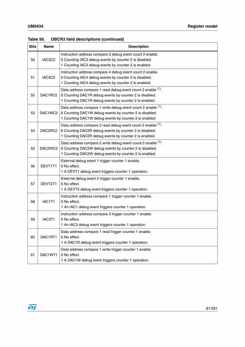
UM0434 Register model
81/391
50 IAC3C2
Instruction address compare 3 debug event count 2 enable.
0 Counting IAC3 debug events by counter 2 is disabled.
1 Counting IAC3 debug events by counter 2 is enabled.
51 IAC4C2
Instruction address compare 4 debug event count 2 enable.
0 Counting IAC4 debug events by counter 2 is disabled.1 Counting IAC4 debug events by counter 2 is enabled.
52 DAC1RC2Data address compare 1 read debug event count 2 enable (1).0 Counting DAC1R debug events by counter 2 is disabled.
1 Counting DAC1R debug events by counter 2 is enabled.
53 DAC1WC2
Data address compare 1 write debug event count 2 enable (1).
0 Counting DAC1W debug events by counter 2 is disabled.
1 Counting DAC1W debug events by counter 2 is enabled.
54 DAC2RC2
Data address compare 2 read debug event count 2 enable (1).
0 Counting DAC2R debug events by counter 2 is disabled.
1 Counting DAC2R debug events by counter 2 is enabled.
55 DAC2WC2
Data address compare 2 write debug event count 2 enable (1).
0 Counting DAC2W debug events by counter 2 is disabled.1 Counting DAC2W debug events by counter 2 is enabled.
56 DEVT1T1External debug event 1 trigger counter 1 enable.0 No effect.
1 A DEVT1 debug event triggers counter 1 operation.
57 DEVT2T1
External debug event 2 trigger counter 1 enable.
0 No effect.
1 A DEVT2 debug event triggers counter 1 operation.
58 IAC1T1
Instruction address compare 1 trigger counter 1 enable.
0 No effect.1 An IAC1 debug event triggers counter 1 operation.
59 IAC3T1Instruction address compare 3 trigger counter 1 enable.0 No effect.
1 An IAC3 debug event triggers counter 1 operation.
60 DAC1RT1
Data address compare 1 read trigger counter 1 enable.
0 No effect.
1 A DAC1R debug event triggers counter 1 operation.
61 DAC1WT1
Data address compare 1 write trigger counter 1 enable.
0 No effect.1 A DAC1W debug event triggers counter 1 operation.
Table 56. DBCR3 field descriptions (continued)
Bits Name Description

Register model UM0434
82/391
Perform updates to DBCR0, DBSR, DBCR3, and DBCNT carefully if the counters are enabled for counting ICMP events. An instruction that updates the counters or control over the counters can cause one or more counter events (DCNT1, DCNT2, CNT1TRG), even if the result of the instruction is to modify the counter value or control value to a state where counter events are not expected. This is due to the pipelined nature of the counter and control operation. ● For DBCNT, if a counter is enabled to count ICMP events, MSR[DE] = 1, and the
counter value is 1 before execution of an mtspr that loads the counter with a different value, a counter event is generated after the mtspr completes, even though the counter is loaded with a new value. When the mtspr finishes executing, a debug event is posted, but the counter holds the newly written value. The new counter value is assigned at the completion of an mtspr that modifies a counter, regardless of whether a debug event is generated based on the old counter value. To avoid this, modify DBCNT and DBCR3 only when there is no possibility of a counter-related debug event on the mtspr.
● For DBCR3, if a counter is enabled to count ICMP events, MSR[DE] = 1, and the counter value is 1 before execution of an mtspr that is loading DBCR3 with a different value, a counter event may be generated after the mtspr completes, even though DBCR3 is loaded with a value that prevents the particular event from being counted. When the mtspr finishes executing, a debug event is posted, but the DBCR3 value reflects the newly established control, which may indicate that the particular event is not to cause a counter update. Modifying DBCR0 to affect counter event enabling/disabling may have similar issues, as may modifying DBSR[CNT1TRG].
4.12.4 Debug status register (DBSR)
DBSR, shown in Table 57, contains status on debug events and the most recent processor reset. Hardware sets DBSR, and software reads and clears it by writing a 1 in any bit position that is to be cleared and 0 in all other bit positions. The write data to the debug status register is not direct data, but a mask. A 1 causes the bit to be cleared, and a 0 has no effect. Debug status bits are set by debug events only while internal debug mode is enabled or external debug mode is enabled. When debug interrupts are enabled (MSR[DE] = 1, DBCR0[IDM] = 1, and DBCR0[EDM] = 0), a set bit in DBSR causes a debug interrupt to be generated.
When debug interrupts are enabled (MSR[DE]=1, DBCR0[IDM]=1, and DBCR0[EDM]=0), a set bit in DBSR other than MRR or VLES causes a debug interrupt. The debug interrupt handler clears DBSR bits before returning to normal execution. The PowerPC VLE APU
62 CNT2T1
Debug counter 2 trigger counter 1 enable.
0 No effect.
1 Counter 2 decrementing to 0 triggers counter 1 operation.
63 CONFIG
Debug counter configuration.
0 Counter 1 and counter 2 are independent counters.1 Counter 1 and counter 2 are concatenated into a single 32-bit counter. The event count control bits for counter 1 are used and the event count control bits for counter 2 are ignored.
1. If the DACx field in DBCR0 is set to restrict events to only reads or only writes, only those events are counted if enabled in DBCR3. In general, DAC events should be disabled in DBCR0.
Table 56. DBCR3 field descriptions (continued)
Bits Name Description

UM0434 Register model
83/391
adds the DBSR[VLES] status bit to indicate debug events occurring due to a PowerPC VLE instruction.
Table 58 provides field definitions for the debug status register.
Table 57. DBSR register
32 33 34 35 36 37 38 39 40 41 42 43 44 45 46 47
Field IDE UDE MRR ICMP BRT IRPT TRAP IAC1 IAC2 IAC3 IAC4 DAC1R DAC1W DAC2R DAC2W
Reset 0001_0000_0000_0000
R/W Read/Clear
48 49 52 53 54 55 56 57 58 59 62 63
Field RET — DEVT1 DEVT2DCNT1DCNT2 CIRPT CRET — CNT1TRG
Reset 0000_0000_0000_0000
R/W Read/Clear
SPR SPR 304
Table 58. DBSR field descriptions
Bits Name Description
32 IDE
Imprecise debug event. Set if MSR[DE] = 0 and DBCR0[EDM] = 0 and a debug event causes its respective debug status register bit to be set. IDE can also be set if DBCR0[EDM] = 1 and an imprecise debug event occurs due to a DAC event on a load or store that is terminated with error, or if an ICMP event occurs in conjunction with a SPE FP round exception.
33 UDE Unconditional debug event. Set when an unconditional debug event occurs.
34–35 MRR
Most recent reset.
00 No reset since software last cleared these bits.
01 A hard reset occurred since software last cleared these bits.
1x Reserved.
36 ICMP Instruction complete debug event. Set if an instruction complete debug event occurs.
37 BRT Branch taken debug event. Set if an branch taken debug event occurs.
38 IRPT Interrupt taken debug event. Set if an interrupt taken debug event occurs.
39 TRAP Trap taken debug event. Set if a trap taken debug event occurs.
40 IAC1 Instruction address compare 1 debug event. Set if an IAC1 debug event occurs.
41 IAC2 Instruction address compare 2 debug event. Set if an IAC2 debug event occurs.
42 IAC3 Instruction address compare 3 debug event. Set if an IAC3 debug event occurs.
43 IAC4 Instruction address compare 4 debug event. Set if an IAC4 debug event occurs.
44 DAC1RData address compare 1 read debug event. Set if a read-type DAC1 debug event occurs while DBCR0[DAC1] = 0b10 or DBCR0[DAC1] = 0b11.
45 DAC1WData address compare 1 write debug event. Set if a write-type DAC1 debug event occurs while DBCR0[DAC1] = 0b01 or DBCR0[DAC1] = 0b11.
46 DAC2RData address compare 2 read debug event. Set if a read-type DAC2 debug event occurs while DBCR0[DAC2] = 0b10 or DBCR0[DAC2] = 0b11.

Register model UM0434
84/391
4.13 Hardware implementation dependent registersHardware implementation-dependent registers 0 and 1 (HID0 and HID1) are configuration registers to control various processor and system functions.
4.13.1 Hardware implementation dependent register 0 (HID0)
HID0, shown in Table 59, is used for various configuration and control functions.
HID0 fields are described in Table 60.
47 DAC2WData address compare 2 write debug event. Set if a write-type DAC2 debug event occurs while DBCR0[DAC2] = 0b01 or DBCR0[DAC2] = 0b11.
48 RET Return debug event. Set if a Return debug event occurs.
49–52 — Reserved, should be cleared.
53 DEVT1 External debug event 1 debug event. Set if a DEVT1 debug event occurs.
54 DEVT2 External debug event 2 debug event. Set if a DEVT2 debug event occurs.
55 DCNT1 Debug counter 1 debug event. Set if a DCNT1 debug event occurs.
56 DCNT2 Debug counter 2 debug event. Set if a DCNT2 debug event occurs.
57 CIRPT Critical interrupt taken debug event. Set if a critical interrupt taken debug event occurs.
58 CRET Critical return debug event. Set if a critical return debug event occurs.
59–62 — Reserved, should be cleared.
63 CNT1TRG Counter 1 triggered. Set if debug counter 1 is triggered by a trigger event.
Table 58. DBSR field descriptions (continued)
Bits Name Description
Table 59. Hardware implementation dependent register 0 (HID0)
32 33 37 38 39 40 41 42 43 45 46 47
Field EMCP — BPRED DOZENAPSLEEP — ICR NHR
Reset All zeros
R/W R/W
48 49 50 51 52 53 54 55 56 63
— TBENSEL_TBCLKDCLREEDCLRCECICLRDEMCCLRDEDAPUEN —
Reset All zeros
R/W R/W
SPR SPR 1008

UM0434 Register model
85/391
Table 60. HID0 field descriptions
Bits Name Description
32 EMCP
Enable machine check signal (p_mcp_b). Used to mask out further machine check exceptions caused by assertion of p_mcp_b.
0 p_mcp_b is disabled.1 p_mcp_b is enabled. If MSR[ME] = 0, asserting p_mcp_b causes checkstop. If MSR[ME] = 1, asserting p_mcp_b causes a machine check interrupt.
33–37 — Reserved, should be cleared.
38–39 BPRED
Branch prediction (acceleration) control. Controls BTB lookahead for branch acceleration. Note that for branches with AA = 1, the msb of the displacement field is still used to indicate forward/backward, even though the branch is absolute. Used in conjunction with BUCSR.
00 Branch acceleration is enabled.01 Branch acceleration is disabled for backward branches.
10 Branch acceleration is disabled for forward branches.
11 Branch acceleration is disabled for both branch directions.
40 DOZE
Doze power management mode. Doze mode is invoked by setting MSR[WE] while DOZE = 1.
0 Doze mode is disabled.
1 Doze mode is enabled.
41 NAP
Nap power management mode. Nap mode is invoked by setting MSR[WE] while NAP=1.
0 Nap mode is disabled.1 Nap mode is enabled.
42 SLEEP
Sleep power management mode. Sleep mode is invoked by setting MSR[WE] while WE=1. Only one of DOZE, NAP, or SLEEP should be set for proper operation.
0 Sleep mode is disabled.1 Sleep mode is enabled.
43–45 — Reserved, should be cleared.
46 ICR
Interrupt inputs clear reservation.
0 External and critical input interrupts do not affect reservation status.1 External and critical input interrupts clear an outstanding reservation.
47 NHR
Not hardware reset. Provided for software use. Set anytime by software, cleared by reset.0 Indicates a reset to a reset exception handler if software has previously set this bit.
1 Indicates to a reset exception handler that there was no reset if software has previously set this bit.
48 — Reserved, should be cleared.
49 TBEN
Time base enable. Used to enable the time base and decrementer.
0 Time base is disabled.1 Time base is enabled.
50SEL_TBCL
K
Select time base clock. Selects the time base clock source. This bit must altered while the time base is disabled to prevent counter glitches. Timer interrupts should be disabled beforehand, and TBL and TBU are reinitialized after a change of time base clock source.
0 Time base is based on processor clock.
1 Time base is based on the p_tbclk input.

Register model UM0434
86/391
4.13.2 Hardware implementation dependent register 1 (HID1)
The HID1 register is used for bus configuration and system control. HID1 is shown in Table 61.
51 DCLREE
Debug interrupt clears MSR[EE]. Controls whether debug interrupts force external input interrupts to be disabled, or whether they remain unaffected.0 MSR[EE] unaffected by debug interrupt.
1 MSR[EE] cleared by debug interrupt.
52 DCLRCE
Debug interrupt clears MSR[CE]. Controls whether debug interrupts force critical interrupts to be disabled, or whether they remain unaffected.0 MSR[CE] unaffected by debug interrupt.
1 MSR[CE] cleared by debug Interrupt.
53 CICLRDE
Critical interrupt clears MSR[DE]. Controls whether certain critical interrupts (critical input, watchdog timer) force debug interrupts to be disabled, or whether they remain unaffected. Machine check interrupts have a separate control bit.
0 MSR[DE] unaffected by critical class interrupt.1 MSR[DE] cleared by critical class interrupt.
If critical interrupt debug events are enabled (DBCR0[CIRPT] is set, which should only be done when the debug APU is enabled), and MSR[DE] is set at the time of a critical interrupt (critical input, watchdog timer), a debug event is generated after the critical interrupt handler has been fetched, and the debug handler is executed first. In this case, DSRR0[DE] will have been cleared, such that after returning from the debug handler, the critical interrupt handler will not be run with MSR[DE] enabled.
54 MCCLRDE
Machine check interrupt clears MSR[DE]. Controls whether machine check interrupts force debug interrupts to be disabled or are unaffected. If critical interrupt debug events are enabled (DBCR0[CIRPT] is set, which should only be done when the debug APU is enabled), and MSR[DE] is set at the time of a machine check interrupt, a debug event is generated after the machine check interrupt handler is fetched, and the debug handler executes first. In this case, DSRR0[DE] is cleared so that after returning from the debug handler, the machine check handler cannot be run if MSR[DE] = 1.
0 MSR[DE] unaffected by machine check interrupt.
1 MSR[DE] cleared by machine check interrupt.
55 DAPUEN
Debug APU enable. Controls whether the debug APU is enabled.
0 Debug APU disabled. Debug interrupts use the critical interrupt resources: CSRR0/CSRR1 and rfci; rfdi is treated as an illegal instruction. DCLREE, DCLRCE, CICLRDE, and MCCLRDE settings are ignored and are assumed to be ones.
1 Debug APU enabled. Debug interrupts use DSRR0/DSRR1 for saving state and rfdi is available for returning from a debug interrupt.
Read and write access to DSRR0/DSRR1 via mfspr and mtspr is not affected by this bit.
56–63 — Reserved, should be cleared.
Table 60. HID0 field descriptions (continued)
Bits Name Description

UM0434 Register model
87/391
HID1 fields are described in Table 62.
4.14 Branch target buffer (BTB) registersThis section describes the only register that controls the branch target buffer.
4.14.1 Branch unit control and status register (BUCSR)
BUCSR, shown in Table 63, is for general control & status of the branch target buffer (BTB).
BUCSR fields are described in Table 64.
Table 61. Hardware implementation dependent register 1 (HID1)
32 55 56 57 62 63
Field — ATS – ARD
Reset All zeros
R/W R/W
SPR SPR 1009
Table 62. HID1 field descriptions
Bits Name Description
32–55 — Reserved, should be cleared.
56 ATSAtomic status (read-only). Indicates state of the reservation bit in the load/store unit. See Chapter 5.7: Memory synchronization and reservation instructions on page 111.”
57–62 — Reserved, should be cleared.
63 ARD
Address retraction disable.
0 Address retraction enabled.
1 Address retraction disabled.Controls Address Retraction operation. For details, see Chapter 9.5.3: Address retraction on page 282.”
Table 63. Branch unit control and status register (BUCSR)
32 53 54 55 62 63
Field — BBFI — BPEN
Reset All zeros
R/W R/W
SPR SPR 1013

Register model UM0434
88/391
4.15 L1 cache configuration registersThis section describes the register that helps not to configure the cache.
4.15.1 L1 cache configuration register 0 (L1CFG0)
The L1 cache configuration register 0 (L1CFG0) provides information on how not to configure the e200z3 cache design. For e200z3, reads of this register return a value of all zeros.
4.16 MMU registersThis section describes the e200z3 registers for setting up and maintaining the TLBs.
4.16.1 MMU control and status register 0 (MMUCSR0)
MMUCSR0, shown in Table 65, controls the state of the MMU.
The MMUCSR0 fields are described in Table 66.
Table 64. Branch unit control and status register
Bits Name Description
32–53 — Reserved, should be cleared.
54 BBFIBranch target buffer flash invalidate. When set, BBFI flash clears the valid bit of all BTB entries; clearing occurs regardless of the value of the enable bit (BPEN).
Note: BBFI is always read as 0.
55–62 — Reserved, should be cleared.
63 BPEN
Branch target buffer (BTB) enable.
0 BTB prediction disabled. No hits are generated from the BTB and no new entries are allocated. Entries are not automatically invalidated when BPEN is cleared; BBFI controls entry invalidation.
1 BTB prediction enabled (enables BTB to predict branches).
Table 65. MMU Control and Status Register 0 (MMUCSR0)
32 61 62 63
Field — TLB1_FI —
Reset All zeros
R/W R/W
SPR SPR 1012

UM0434 Register model
89/391
4.16.2 MMU configuration register (MMUCFG)
The MMU configuration register (MMUCFG) is a 32-bit read-only register. The SPR number for MMUCFG is 1015 in decimal. MMUCFG, which provides information about the configuration of the e200z3 MMU design, is shown in Table 67.
The MMUCFG fields are described in Table 68.
Table 66. MMUCSR0 field descriptions
Bits Name Description
32–61 — Reserved, should be cleared.
62 TLB1_FI
TLB1 flash invalidate
0 No flash invalidate
1 TLB1 invalidation operation. Hardware initiates a TLB1 invalidation, after which TLB1_FI is cleared. Setting TLB1_FI while an invalidation operation is in progress causes an undefined operation. Clearing TLB1_FI while an invalidation operation is in progress is ignored. TLB1 invalidation operations require 3 cycles to complete.
63 — Reserved, should be cleared.
Table 67. MMU configuration register 1 (MMUCFG)
32 48 49 52 53 57 58 59 60 61 62 63
Field — NPIDS PIDSIZE — NTLBS MAVN
Reset 0000_0000_0000_0000_0 000_1 001_11 00 01 00
R/W Read only
SPR SPR 1015

Register model UM0434
90/391
4.16.3 TLB configuration registers (TLBnCFG)
The TLBnCFG read-only registers provide information about each specific TLB that is visible to the programming model.
TLB configuration register 0 (TLB0CFG)
TLB0CFG, shown in Table 69, provides information about the configuration of TLB0. Because the e200z3 MMU design does not implement TLB0, this register reads as all zeros. It is supplied to allow software to query it in a way compatible with other Book E designs.
The TLB0CFG fields are described in Table 70.
Table 68. MMUCFG field descriptions
Bits Name Description
32–48 — Reserved, should be cleared.
49–52 NPIDSNumber of PID registers.
0001 This version of the MMU implements one PID register (PID0).
53–57 PIDSIZEPID register size.
00111 PID registers contain 8 bits in this version of the MMU.
58–59 — Reserved, should be cleared.
60–61 NTLBS
Number of TLBs.
01 This version of the MMU implements two TLB structures: a null TLB0 and a populated TLB1.
62–63 MAVNMMU architecture version number.
00 This version of the MMU implements version 1.0 of the Book E MMU architecture.
Table 69. TLB configuration register 0 (TLB0CFG)
32 39 40 43 44 47 48 49 50 51 52 63
Field ASSOC MINSIZE MAXSIZE IPROT AVAIL — NENTRY
Reset All zeros (TLB0 is not implemented)
R/W Read only
SPR SPR 688
Table 70. TLB0CFG field descriptions
Bits Name Description
32–39 ASSOC Associativity.
40–43 MINSIZE Minimum page size.
44–47 MAXSIZEMaximum page size.
0
48 IPROTInvalidate protect capability.
0

UM0434 Register model
91/391
TLB configuration register 1 (TLB1CFG)
TLB1CFG, shown in Table 71, provides information on the TLB1 configuration.
The TLB1CFG fields are described in Table 72.
4.16.4 MMU assist registers (MAS0–MAS4, MAS6)
The e200z3 uses six special purpose registers (MAS0–MAS4, and MAS6) for reading, writing, and searching the TLBs. The MAS registers can be read or written using the mfspr and mtspr instructions. The e200z3 does not implement the MAS5 register, which is present in other Book E designs, because the tlbsx instruction only searches based on a single SPID value.
49 AVAILPage size availability.
0
50–51 — Reserved, should be cleared.
52–63 NENTRYNumber of entries.
0 TLB0 contains 0 entries.
Table 70. TLB0CFG field descriptions (continued)
Bits Name Description
Table 71. TLB configuration register 1 (TLB1CFG)
32 39 40 43 44 47 48 49 50 51 52 63
Field ASSOC MINSIZE MAXSIZE IPROT AVAIL — NENTRY
Reset 0010_0000 0001 1001 1 1 00 0000_0010_0000
R/W Read only
SPR SPR 689
Table 72. TLB1CFG field descriptions
Bits Name Description
32–39 ASSOCAssociativity.0x10 Indicates that TLB1 associativity is 16
40–43 MINSIZEMinimum page size.0x1 Smallest page size is 4 Kbytes.
44–47 MAXSIZEMaximum page size.0x9 Largest page size is 256 Mbytes.
48 IPROTInvalidate protect capability.1 Invalidate protect capability is supported in TLB1.
49 AVAILPage size availability.1 All page sizes between MINSIZE and MAXSIZE are supported.
50–51 — Reserved, should be cleared.
52–63 NENTRYNumber of entries.
0x010 TLB1 contains 16 entries.

Register model UM0434
92/391
For details on the MASn registers, see Chapter 7.6.5: MMU assist registers (MAS) on page 204.” The MAS0 register is shown in Table 73.
MAS0 fields are defined in Table 74.
The MAS1 register is shown in Table 75.
MAS1 fields are defined in Table 76.
Table 73. MAS Register 0 (MAS0) Format
32 33 34 35 36 42 43 47 48 58 59 63
Field — TLBSEL — ESEL — NV
Reset Undefined on m_por assertion, unchanged on p_reset_b assertion
R/W R/W
SPR SPR 624
Table 74. MAS0 - MMU read/write and replacement control
Bits Name Description
32–33 — Reserved, should be cleared.
34–35 TLBSELSelects TLB for access.
01 TLB1 (ignored by the e200z3, should be written to 01 for future compatibility).
36–42 — Reserved, should be cleared.
43–47 ESEL Entry select for TLB1.
48–58 — Reserved, should be cleared.
59–63 NVNext replacement victim for TLB1 (software managed). Software updates this field; it is copied to the ESEL field on a TLB error (See Table 156).
Table 75. MMU assist register 1 (MAS1)
32 33 34 39 40 47 48 50 51 52 55 56 63
Field VALID IPROT — TID — TS TSIZE —
Reset Undefined on m_por assertion, unchanged on p_reset_b assertion
R/W R/W
SPR SPR 625

UM0434 Register model
93/391
The MAS2 register is shown in Table 77.
MAS2 fields are defined in Table 78.
Table 76. MAS1 - descriptor context and configuration control
Bits Name Description
32 VALIDTLB entry valid.0 This TLB entry is invalid.
1 This TLB entry is valid.
33 IPROT
Invalidation protect. Protects TLB entry from invalidation by tlbivax (TLB1 only), or flash invalidates through MMUCSR0[TLB1_FI].
0 Entry is not protected from invalidation.
1 Entry is protected from invalidation as described in Chapter 7.3.1: IPROT invalidation protection in TLB1 on page 198.”
34–39 — Reserved, should be cleared.
40–47 TIDTranslation ID. Compared with the current process IDs of the effective address to be translated. A TID value of 0 defines an entry as global and matches with all process IDs.
48–50 — Reserved, should be cleared.
51 TSTranslation address space. Compared with MSR[IS] or MSR[DS] (depending on the type of access) to determine if this TLB entry may be used for translation.
52–55 TSIZE
Entry page size.
Supported page sizes are:
0001 4 Kbytes 0110 4 Mbytes.
0010 16 Kbytes 0111 16 Mbytes.
0011 64 Kbytes 1000 64 Mbytes.
0100 256 Kbytes 1001 256 Mbytes.
0101 1 Mbyte.All other values are undefined.
56–63 — Reserved, should be cleared.
Table 77. MMU assist register 2 (MAS2)
SPR 626 Access: Supervisor read/write
0 32
REPN
W
Reset Undefined
32 51 52 54 55 56 57 58 59 60 61 62 63
REPN — VLE W I M G E
W
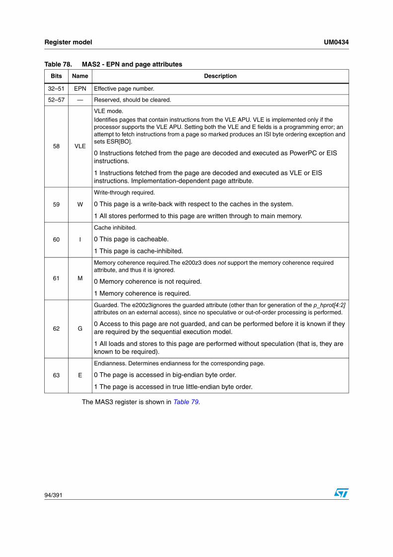
Register model UM0434
94/391
The MAS3 register is shown in Table 79.
Table 78. MAS2 - EPN and page attributes
Bits Name Description
32–51 EPN Effective page number.
52–57 — Reserved, should be cleared.
58 VLE
VLE mode.
Identifies pages that contain instructions from the VLE APU. VLE is implemented only if the processor supports the VLE APU. Setting both the VLE and E fields is a programming error; an attempt to fetch instructions from a page so marked produces an ISI byte ordering exception and sets ESR[BO].
0 Instructions fetched from the page are decoded and executed as PowerPC or EIS instructions.
1 Instructions fetched from the page are decoded and executed as VLE or EIS instructions. Implementation-dependent page attribute.
59 W
Write-through required.
0 This page is a write-back with respect to the caches in the system.
1 All stores performed to this page are written through to main memory.
60 I
Cache inhibited.
0 This page is cacheable.
1 This page is cache-inhibited.
61 M
Memory coherence required.The e200z3 does not support the memory coherence required attribute, and thus it is ignored.
0 Memory coherence is not required.
1 Memory coherence is required.
62 G
Guarded. The e200z3ignores the guarded attribute (other than for generation of the p_hprot[4:2] attributes on an external access), since no speculative or out-of-order processing is performed.
0 Access to this page are not guarded, and can be performed before it is known if they are required by the sequential execution model.
1 All loads and stores to this page are performed without speculation (that is, they are known to be required).
63 E
Endianness. Determines endianness for the corresponding page.
0 The page is accessed in big-endian byte order.
1 The page is accessed in true little-endian byte order.

UM0434 Register model
95/391
MAS3 fields are defined in Table 80.
The MAS4 register, shown in Table 81, contains fields for specifying default information to be pre-loaded on certain MMU related exceptions.
The MAS4 fields are defined in Table 82.
Table 79. MMU assist register 3 (MAS3)
Permission bits
32 51 52 53 54 55 56 57 58 59 60 61 62 63
Field RPN — U0 U1 U2 U3 UX SX UW SW UR SR
Reset Undefined on m_por assertion, unchanged on p_reset_b assertion
R/W R/W
SPR SPR 627
Table 80. MAS3 - RPN and access control
Bits Name Description
32–51 RPNReal page number.
Only bits that correspond to a page number are valid. Bits that represent offsets within a page are ignored and should be zero.
52–53 — Reserved, should be cleared.
54–57 U0–U3 User bits.
58–63 PERMIS Permission bits (UX, SX, UW, SW, UR, SR).
Table 81. MMU assist register 4 (MAS4)
SPR 628 Access: Supervisor read/write
32 33 34 35 36 39 40 47 48 51 52 55 56 57 58 59 60 61 62 63
R— TLBSELD — TIDSELD — TSIZED — VLED WD ID MD GD ED
W
Reset All zeros
Table 82. MAS4 - hardware replacement assist configuration register
Bits Name Description
32–33 — Reserved, should be cleared.
34–35 TLBSELDDefault TLB selected.
01 TLB1 (ignored by the e200z3, should be written to 01 for future compatibility)
36–43 — Reserved, should be cleared.
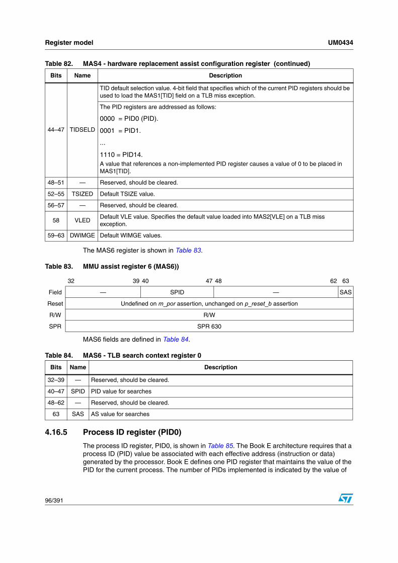
Register model UM0434
96/391
The MAS6 register is shown in Table 83.
MAS6 fields are defined in Table 84.
4.16.5 Process ID register (PID0)
The process ID register, PID0, is shown in Table 85. The Book E architecture requires that a process ID (PID) value be associated with each effective address (instruction or data) generated by the processor. Book E defines one PID register that maintains the value of the PID for the current process. The number of PIDs implemented is indicated by the value of
44–47 TIDSELD
TID default selection value. 4-bit field that specifies which of the current PID registers should be used to load the MAS1[TID] field on a TLB miss exception.
The PID registers are addressed as follows:
0000 = PID0 (PID).
0001 = PID1.
...
1110 = PID14.A value that references a non-implemented PID register causes a value of 0 to be placed in MAS1[TID].
48–51 — Reserved, should be cleared.
52–55 TSIZED Default TSIZE value.
56–57 — Reserved, should be cleared.
58 VLEDDefault VLE value. Specifies the default value loaded into MAS2[VLE] on a TLB miss exception.
59–63 DWIMGE Default WIMGE values.
Table 82. MAS4 - hardware replacement assist configuration register (continued)
Bits Name Description
Table 83. MMU assist register 6 (MAS6))
32 39 40 47 48 62 63
Field — SPID — SAS
Reset Undefined on m_por assertion, unchanged on p_reset_b assertion
R/W R/W
SPR SPR 630
Table 84. MAS6 - TLB search context register 0
Bits Name Description
32–39 — Reserved, should be cleared.
40–47 SPID PID value for searches
48–62 — Reserved, should be cleared.
63 SAS AS value for searches

UM0434 Register model
97/391
MMUCFG[NPIDS]. (The e200z3 defines no additional PID registers.) PID values are used to construct virtual addresses for accessing memory.
4.17 Support for fast context switchingTo provide real-time capabilities for embedded systems, future versions of the e200z3 core will include optional hardware support for fast context switching. The initial version of the e200z3 does not implement additional register contexts.
4.17.1 Context control register (CTXCR)
The future versions of the e200z3 core may include optional hardware support for fast context switching to provide real-time capabilities for embedded systems. The initial version of e200z3 does not implement additional register contexts. A new privileged 32-bit special-purpose register (SPR) called the context control register (CTXCR) is defined in the core CPU. The CTXCR controls the context registers that are mapped to the current context and holds current, alternate, and saved context information. Supervisor software reads the CTXCR to determine whether multiple contexts are supported in hardware, and if so, the number implemented. When multiple register contexts are present (CTXCR[NUMCTX] is non-zero), CTXCR is also writable. Otherwise, writes are ignored, and the register reads as all zeros. CTXCR is shown in Table 86.
4.18 SPR register accessSPRs are accessed with the mfspr and mtspr instructions. The following sections outline additional access requirements.
4.18.1 Invalid SPR references
System behavior when an invalid SPR is referenced depends on the apparent privilege level of the register, which is determined by bit 5 in the SPR address. If the invalid SPR is
Table 85. Process ID register (PID0)
32 55 56 63
Field — Process ID
Reset All zeros
R/W R/W
SPR SPR 48
Table 86. Context control register (CTXCR)
32 55 56 63
Field —
Reset All zeros
R/W R/W (Writes are ignored because no additional contexts are implemented.)
SPR SPR 560

Register model UM0434
98/391
accessible in user mode, an illegal exception is generated. If the invalid SPR is accessible only in supervisor mode and the CPU core is in supervisor mode (MSR[PR] = 0), an illegal exception is generated. If the invalid SPR address is accessible only in supervisor mode and the CPU is not in supervisor mode (MSR[PR] = 1), a privilege exception is generated.
4.18.2 Synchronization requirements for SPRs
Except for the following registers, no synchronization is required for accessing SPRs beyond those stated in Book E. EREF completely describes synchronization requirements. Software requirements for synchronization before/after accessing these registers are shown in Table 88. The notation CSI in the table refers to context synchronizing instructions, including sc, isync, rfi, rfci, and rfdi.
Table 87. System response to invalid SPR reference
SPR address bit 5 Mode MSR[PR] Response
0 — — Illegal exception
1 Supervisor 0 Illegal exception
1 User 1 Privilege exception
Table 88. Additional synchronization requirements for SPRs
Context altering event or instruction Required before Required after Notes
mtmsr[UCLE] None CSI
mfspr
DBCNT Debug counter register msync None (1)
DBSR Debug status register msync None
HID0 Hardware implementation dependent register 0 None None
HID1 Hardware implementation dependent register 1 msync None
MMUCSR MMU control and status register 0 CSI None
mtspr
BUCSR Branch unit control and status register None CSI
CTXCR Context control register CSI CSI
DBCNT Debug counter register None CSI (1)
DBCR0 Debug control register 0 None CSI
DBCR1 Debug control register 1 None CSI
DBCR2 Debug control register 2 None CSI
DBCR3 Debug control register 3 None CSI
DBSR Debug status register msync None
HID0 Hardware implementation dependent reg 0 CSI CSI
MMUCSR MMU control and status register 0 CSI CSI
1. Not required if counter is not currently enabled.

UM0434 Register model
99/391
4.18.3 Special purpose register summary
PowerPC Book E and implementation-specific SPRs for the e200z3 core are listed in Table 89. All registers are 32 bits. Register bits are numbered from bit 32–63 (most significant to least significant). Shaded entries represent optional registers. An SPR can be read or written with the mfspr and mtspr instructions. In the instruction syntax, compilers should recognize the mnemonic in the table below. For details, see Chapter 4.4: Processor control registers on page 43.”
Table 89. Special purpose registers
Mnemonic NameSPR
numberAccess Privileged
e200z3 specific
BUCSR Branch unit control and status register 1013 R/W Yes Yes
CSRR0 Critical save/restore register 0 58 R/W Yes No
CSRR1 Critical save/restore register 1 59 R/W Yes No
CTR Count register 9 R/W No No
CTXCR Context control register 560 R/W(1) Yes Yes
DAC1 Data address compare 1 316 R/W Yes No
DAC2 Data address compare 2 317 R/W Yes No
DBCNT Debug counter register 562 R/W Yes Yes
DBCR0 Debug control register 0 308 R/W Yes No
DBCR1 Debug control register 1 309 R/W Yes No
DBCR2 Debug control register 2 310 R/W Yes No
DBCR3 Debug control register 3 561 R/W Yes Yes
DBSR Debug status register 304 Read/Clear(2) Yes No
DEAR Data exception address register 61 R/W Yes No
DEC Decrementer 22 R/W Yes No
DECAR Decrementer auto-reload 54 R/W Yes No
DSRR0 Debug save/restore register 0 574 R/W Yes Yes
DSRR1 Debug save/restore register 1 575 R/W Yes Yes
ESR Exception syndrome register 62 R/W Yes No
HID0 Hardware implementation dependent reg 0 1008 R/W Yes Yes
HID1 Hardware implementation dependent reg 1 1009 R/W Yes Yes
IAC1 Instruction address compare 1 312 R/W Yes No
IAC2 Instruction address compare 2 313 R/W Yes No
IAC3 Instruction address compare 3 314 R/W Yes No
IAC4 Instruction address compare 4 315 R/W Yes No
IVOR0 Interrupt vector offset register 0 400 R/W Yes No
IVOR1 Interrupt vector offset register 1 401 R/W Yes No
IVOR2 Interrupt vector offset register 2 402 R/W Yes No

Register model UM0434
100/391
IVOR3 Interrupt vector offset register 3 403 R/W Yes No
IVOR4 Interrupt vector offset register 4 404 R/W Yes No
IVOR5 Interrupt vector offset register 5 405 R/W Yes No
IVOR6 Interrupt vector offset register 6 406 R/W Yes No
IVOR7 Interrupt vector offset register 7 407 R/W Yes No
IVOR8 Interrupt vector offset register 8 408 R/W Yes No
IVOR9(3) Interrupt vector offset register 9 409 R/W Yes No
IVOR10 Interrupt vector offset register 10 410 R/W Yes No
IVOR11 Interrupt vector offset register 11 411 R/W Yes No
IVOR12 Interrupt vector offset register 12 412 R/W Yes No
IVOR13 Interrupt vector offset register 13 413 R/W Yes No
IVOR14 Interrupt vector offset register 14 414 R/W Yes No
IVOR15 Interrupt vector offset register 15 415 R/W Yes No
IVOR32 Interrupt vector offset register 32 528 R/W Yes Yes
IVOR33 Interrupt vector offset register 33 529 R/W Yes Yes
IVOR34 Interrupt vector offset register 34 530 R/W Yes Yes
IVPR Interrupt vector prefix register 63 R/W Yes No
LR Link register 8 R/W No No
L1CFG0 L1 cache configuration register 0 515 Read only No Yes
MAS0 MMU assist register 0 624 R/W Yes Yes
MAS1 MMU assist register 1 625 R/W Yes Yes
MAS2 MMU assist register 2 626 R/W Yes Yes
MAS3 MMU assist register 3 627 R/W Yes Yes
MAS4 MMU assist register 4 628 R/W Yes Yes
MAS6 MMU assist register 6 630 R/W Yes Yes
MCSR Machine check syndrome register 572 R/W Yes Yes
MMUCFG MMU configuration register 1015 Read only Yes Yes
MMUCSR0 MMU control and status register 0 1012 R/W Yes Yes
PID0 Process ID register 48 R/W Yes No
PIR Processor ID register 286 Read only Yes No
PVR Processor version register 287 Read only Yes No
SPEFSCR SPE APU status and control register 512 R/W No No
SPRG0 SPR general 0 272 R/W Yes No
SPRG1 SPR general 1 273 R/W Yes No
Table 89. Special purpose registers (continued)
Mnemonic NameSPR
numberAccess Privileged
e200z3 specific

UM0434 Register model
101/391
4.18.4 Reset settings
Table 90 shows the state of the PowerPC Book E registers and other optional resources immediately following a system reset.
SPRG2 SPR general 2 274 R/W Yes No
SPRG3 SPR general 3 275 R/W Yes No
SPRG4 SPR general 4260 Read only No No
276 R/W Yes No
SPRG5 SPR general 5261 Read only No No
277 R/W Yes No
SPRG6 SPR general 6262 Read only No No
278 R/W Yes No
SPRG7 SPR general 7263 Read only No No
279 R/W Yes No
SRR0 Save/restore register 0 26 R/W Yes No
SRR1 Save/restore register 1 27 R/W Yes No
SVR System version register 1023 Read only Yes Yes
TBL Time base lower268 Read only No No
284 Write only Yes No
TBU Time base upper269 Read only No No
285 Write only Yes No
TCR Timer control register 340 R/W Yes No
TLB0CFG TLB0 configuration register 688 Read only Yes Yes
TLB1CFG TLB1 configuration register 689 Read only Yes Yes
TSR Timer status register 336 Read/Clear(4) Yes No
USPRG0 User SPR general 0 256 R/W No No
XER Integer exception register 1 R/W No No
Notes:
1. Only writable when multiple contexts are implemented. Otherwise, writes are ignored
2. The debug status register (DBSR) is read using mfspr. DBSR cannot be directly written. Instead, DBSR bits corresponding to 1 bits in the GPR can be cleared using mtspr.
3. IVOR9 handles the auxiliary processor unavailable interrupt. This interrupt is defined by the EIS but not supported in the e200z3; therefore, use of IVOR9 is not supported in the e200z3.
4. TSR is read using mfspr, but it cannot be directly written. Instead, TSR bits corresponding to 1 bits in the GPR can be cleared using mtspr.
Table 89. Special purpose registers (continued)
Mnemonic NameSPR
numberAccess Privileged
e200z3 specific

Register model UM0434
102/391
Table 90. Reset settings for e200z3 resources
Resource System reset setting
Program counter p_rstbase[0:19] || 0xFFC
GPRs Unaffected(1)
CR Unaffected 1
BUCSR 0x0000_0000
CSRR0 Unaffected 1
CSRR1 Unaffected 1
CTR Unaffected 1
CTXCR 000 || NUMCTX || 00_0000_0000_0000_0000_0000_0000(2)
DAC1–DAC2 0x0000_0000
DBCNT Unaffected 1
DBCR0–DBCR3 0x0000_0000
DBSR 0x1000_0000
DEAR Unaffected 1
DEC Unaffected 1
DECAR Unaffected 1
DSRR0 Unaffected 1
DSRR1 Unaffected 1
ESR 0x0000_0000
HID0–HID1 0x0000_0000
IAC1–IAC4 0x0000_0000
IVOR0–IVOR15 Unaffected 1
IVOR32–IVOR34 Unaffected 1
IVPR Unaffected 1
L1CFG0(3) —
LR Unaffected 1
MAS0–MAS4, MAS6 Unaffected 1
MCSR 0x0000_0000
MMUCFG 3 —
MMUCSR0 0x0000_0000
MSR 0x0000_0000
PID0 0x0000_0000
PIR 3 0x0000_00 || p_cpuid[0:7]
PVR 3 —
SPEFSCR 0x0000_0000
SPRG0–SPRG7 Unaffected 1

UM0434 Register model
103/391
4.19 Parallel signature unit registersTo support applications requiring system integrity checking during operation, the e200z3 provides a Parallel Signature unit to monitor the CPU data read and data write AHB buses and to accumulate a pair of 32-bit MISR signatures of the data values transferred over these buses.
The primitive polynomial used is P(X)=1+X10+X30+X31+X32. Values are accumulated based on an initially programmed seed value and are qualified based on active byte lanes of the data read and data write buses (p_d_hrdata[63:0], p_d_hwdata[63:0]) as indicated via the p_d_hbstrb[7:0] signals. Inactive byte lanes use a value of all zeros as input data to the MISRs. Refer to Table 170 for active byte lane information. If a transfer error occurs on any accumulated read data, the returned read data is ignored, a value of all zeros is used instead, and the error is logged. Errors occurring on data writes are not logged, since the data driven by the CPU is valid.
The unit can be independently enabled for read cycles and write cycles, allowing for flexible usage. Software can also control accumulation of software-provided values via a pair of update registers. In addition, there is a counter for software to monitor the number of beats of data compressed.
Updates are performed when the parallel signature registers are initialized, when a qualified bus cycle is terminated, when a software update is performed via a high or low update register, and when the parallel signature high or low registers are written with an mtdcr instruction.
Note: Updates due to qualified bus transfers are suppressed for the duration of a debug session.
SRR0 Unaffected 1
SRR1 Unaffected 1
SVR 3 —
TBL Unaffected 1
TBU Unaffected 1
TCR 0x0000_0000
TLB0CFG– TLB1CFG —
TSR Undefined on power-on reset; otherwise, 0x(0b00||WRS)000_0000
USPRG0 Unaffected 1
XER 0x0000_0000
1. Undefined on m_por assertion, unchanged on p_reset_b assertion.
2. For CTXCR 0 only, others unaffected.
3. Read-only register.
Table 90. Reset settings for e200z3 resources (continued)
Resource System reset setting

Register model UM0434
104/391
Figure 6. Parallel signature unit
The parallel signature unit consists of seven registers as described in this section. Access to these registers is privileged. No user-mode access is allowed.
Note: Proper access of the PSU registers requires an mfdcr that reads a PSU register to be proceeded by either mbar or msync. To ensure that the effects of an mtdcr to one of the PSU registers takes effect, the mtdcr is followed by a context synchronizing instruction (sc, isync, rfi, rfci, rfdi).
4.19.1 Parallel signature control register (PSCR)
PSCR, shown in Table 91, controls operation of the parallel signature unit.
PSCR field descriptions are shown in Table 92.
.
+d q
+d q
+d q
+d q
+d q
+d q
+d q... ...
D31 (D63) D30 (D62) D29 (D61) D28 (D60) D1 (D33) D0 (D32)D21 (D53)
+d q
D20 (D52)
+d q
D22 (D54)
Data Bus (p_d_hrdata, p_d_hwdata)
PSHR, (PSLR)
Table 91. Parallel signature control register (PSCR)
32 57 58 59 60 61 62 63
Field — CNTEN — RDEN WREN INIT
Reset All zeros
R/W R/W
DCR DCR 272
Table 92. PSCR field descriptions
Bits Name Description
32–57 — Reserved, should be cleared.
58 CNTEN
Counter enable.
0 Counter is disabled.
1 Counter is enabled. Counter is incremented on every accumulated transfer or on an mtdcr psulr,rS.
59–60 — Reserved, should be cleared.
61 RDEN
Read enable.
0 Processor data read cycles are ignored.
1 Processor data reads cycles are accumulated. For inactive byte lanes, zeros are used for the data values.

UM0434 Register model
105/391
4.19.2 Parallel signature status register (PSSR)
PSSR, shown in Table 93, provides status relative to operation of the parallel signature unit.
The PSSR register fields are described in Table 94.
.
4.19.3 Parallel signature high register (PSHR)
The PSHR, shown in Table 4.19.4, provides signature information for the high word (bits 63–32) of the AHB data read and data write buses. Writing PSHR initializes a seed value before enabling signature accumulation. PSCR[INIT] may also be used to clear the PSHR. PSHR is unaffected by system reset, thus should be initialized by software before performing parallel signature operations.
62 WREN
Write enable.
0 Processor write cycles are ignored.
1 Processor write cycles are accumulated. For inactive byte lanes, zeros are used for the data values.
63 INITThis bit can be written with a 1 to set the values in the PSHR, PSLR, and PSCTR registers to all 0s. (0x00000000). This bit always reads as 0.
Table 92. PSCR field descriptions (continued)
Bits Name Description
Table 93. parallel signature status register (PSSR)
32 62 63
Field — TERR
Reset Unaffected
R/W — w1c
DCR DCR 273
Table 94. PSSR field descriptions
Bits Name Description
32–62 — Reserved, should be cleared.
63 TERR
Transfer error status. Indicates whether a transfer error occurs on accumulated read data and that the read data values returned are ignored and 0s are used instead. Hardware does not clear TERR; only a software write of 1 to TERR clears it.
0 No transfer error on accumulated read data since software last cleared this bit.
1 A transfer error occurred on accumulated read data since software last cleared this bit.

Register model UM0434
106/391
4.19.4 Parallel signature low register (PSLR)
PSLR, shown in Table 4.19.5, provides signature information for the low word (bits 31-0) of the AHB data read and data write buses. Writing PSLR initializes a seed value prior to enabling signature accumulation. PSCR[INIT] can also be used to clear the PSLR. PSLR is unaffected by system reset, thus should be initialized by software prior to performing parallel signature operations.
4.19.5 Parallel signature counter register (PSCTR)
PSCTR, shown in Table 4.19.6, provides count information for signature accumulation. It is incremented on every accumulated transfer or on an mtdcr psulr,rS. Writing to PSCTR initializes a value before enabling signature accumulation. PSCR[INIT] can also be used to clear PSCTR. PSCTR is unaffected by system reset, thus should be initialized by software before performing parallel signature operations.
.
4.19.6 Parallel signature update high register (PSUHR)
PSUHR, shown in Table 98, updates the high signature value via software. It can be written via an mtdcr psuhr, rS instruction to cause signature accumulation to occur in the PSHR using the data value written. Writing to this register does not cause the PSCTR to increment.
Table 95. Parallel signature high register (PSHR)
32 63
Field High signature
Reset Unaffected
R/W R/W
DCR DCR 274
Table 96. Parallel signature low register (PSLR)
32 63
Field Low signature
Reset Unaffected
R/W R/W
DCR DCR 275
Table 97. Parallel signature counter register (PSCTR)
32 63
Field Counter
Reset Unaffected
R/W R/W
DCR DCR 276

UM0434 Register model
107/391
4.19.7 Parallel signature update low register (PSULR)
PSULR, shown in Table 99, updates the low signature value via software. Writing to PSULR causes signature accumulation in the parallel signature low register (PSLR) using the data value written. Writing to this register causes PSCTR to increment.
Table 98. Parallel signature update high register (PSUHR)
32 63
Field High signature update data
Reset Unaffected
R/W Write only
DCR DCR 277
Table 99. Parallel signature update low register (PSULR)
32 63
Field Low signature update data
Reset Unaffected
R/W Write only
DCR DCR 278

Instruction model UM0434
108/391
5 Instruction model
This chapter provides additional information about the Book E architecture as it relates specifically to the e200z3.
The e200z3 is a 32-bit implementation of the Book E architecture. The Book E architecture specification includes a recognition that different processor implementations may require clarifications, extensions, or deviations from the architectural descriptions. Book E instructions are described in the EREF: A Programmer's Reference Manual for Freescale Book E Processors.
5.1 Operand conventionsThis section describes operand conventions as they are represented in the Book E architecture. These conventions follow the basic descriptions in the classic PowerPC architecture with some changes in terminology. For example, distinctions between user- and supervisor-level instructions are maintained, but the designations—UISA, VEA, and OEA—do not apply. Detailed descriptions are provided on conventions used for storing values in registers and memory, for accessing processor registers, and for representing data.
5.1.1 Data organization in memory and data transfers
Bytes in memory are numbered consecutively starting with 0. Each number is the address of the corresponding byte.
Memory operands can be bytes, half-words, words, or double-words (consisting of two 32-bit elements) or, for the load/store multiple instruction type, a sequence of bytes or words. The address of a memory operand is the address of its first byte (that is, of its lowest-numbered byte). Operand length is implicit for each instruction.
5.1.2 Alignment and misaligned accesses
The e200z3 core provides hardware support for misaligned memory accesses; however, there is performance degradation for accesses that cross a 64-bit (8-byte) boundary. For loads that hit in the cache, the throughput of the load/store unit is degraded to 1 misaligned load every 2 cycles. Stores misaligned across a 64-bit (8 byte) boundary can be translated at a rate of 2 cycles per store. Frequent use of misaligned memory accesses is discouraged because of the impact on performance.
Note: Accesses that cross a translation boundary may be restarted. A misaligned access that crosses a page boundary is restarted entirely if the second portion of the access causes a TLB miss. This may result in the first portion being accessed twice.Accesses that cross a translation boundary where the endianness changes cause a byte-ordering data storage interrupt.
Note: lmw, stmw, lwarx, and stwcx. instructions that are not word aligned cause an alignment exception.
5.1.3 e200z3 Floating-Point implementation
The e200z3 core does not implement the floating-point instructions as they are defined in Book E. Attempts to execute a Book E–defined floating-point instruction result in an illegal

UM0434 Instruction model
109/391
instruction exception. However, the vector SPFP APU supports single-precision vector (64-bit, two 32-bit operand) instructions, and the scalar SPFP APU performs single-precision floating-point operations using the lower 32 bits of the GPRs. These instructions are described in Chapter 5.10.4: Embedded vector and scalar single precision floating point APU instructions on page 120.” Unlike the PowerPC UISA, the SPFP APUs store floating-point values as single-precision values in true 32-bit, single-precision format rather than in a 64-bit double-precision format used with FPRs.
5.2 Unsupported instructions and instruction formsBecause the e200z3 is a 32-bit Book E core, all of the instructions defined for 64-bit implementations of the Book E architecture are illegal on the e200z3 and cause an illegal instruction exception type program interruption. The e200z3 core does not support the instructions listed in Table 100. An unimplemented instruction or floating-point-unavailable exception is generated if the processor attempts to execute one of these instructions.
5.3 Optionally supported instructions and instruction formsThe e200z3 core optionally supports the instructions listed in Table 101 if a cache and/or TLB is present. An instruction exception may be generated if the processor attempts to execute one of these instructions and the related functional block is not present, or the specific instruction may be treated as a no-op.
5.4 Implementation-Specific instructionsBook E defines some instructions that are implementation specific. Table 102 summarizes the e200z3 implementation-specific instructions.
Table 100. List of unsupported instructions
Type/Name Mnemonics
String Instructions lswi, lswx, stswi, stswx
Floating Point Instructions fxxxx, lfxxxx, sfxxxx, mcrfs, mffs, mtfxxx
Device control register and Move from APID mfapidi, mfdcrx, mtdcrx
Table 101. List of optionally supported instructions
Type/name Mnemonics Unit
Cache management instructions
dcba, dcbf, dcbi, dcbt, dcbtst, dcbst, dcbzicbi, icbt
Data cache/unified cache
Instruction cache/unified cache
Cache locking instructionsdcbtls, dcbtstls, dcblc
icbtls, icblc
Data cache/unified cache
Instruction cache/unified cache
TLB management instructions
tlbivax, tlbre, tlbsx, tlbsync, tlbwe TLB
DCR management mfdcr, mtdcr DCR

Instruction model UM0434
110/391
5.5 BookE instruction extensionsThe variable length encoding (VLE) provides an extension to 32-bit PowerPC Book E. There are additional operations defined using an alternate instruction encoding to enable reduced code footprint. This alternate encoding set is selected on an instruction page basis. A single page attribute bit selects between standard PowerPC Book E instruction encodings and VLE instructions for that page of memory. This page attribute is an extension to the PowerPC Book E page attributes. Pages can be freely intermixed, allowing for a mixture of code using both types of encodings.
Instruction encodings in pages marked as using the VLE extension are either 16 or 32 bits long, and are aligned on 16-bit boundaries. Therefore, all instruction pages marked as VLE are required to use big-endian byte ordering.
This section describes the various extensions to Book E instructions to support the VLE extension.
rfci, rfdi, rfi—no longer mask bit 62 of CSRR0, DSRR0, or SRR0 respectively. The destination address is [D,C]SRR0[32:62] || 0b0.
bclr, bclrl, bcctr, bcctrl—no longer mask bit 62 of the LR or CTR respectively. The destination address is [LR,CTR][32:62] || 0b0.
5.6 Memory access alignment supportThe e200z3 core provides hardware support for unaligned memory accesses. However, there is a performance degradation for accesses that cross a 64-bit (8 byte) boundary. For these cases, the throughput of the load/store unit is degraded to one misaligned load every 2 cycles. Stores misaligned across a 64-bit (8 byte) boundary can be translated at a rate of 2 cycles per store. Frequent use of unaligned memory accesses is discouraged because of the impact on performance.
Table 102. Implementation-Specific instruction summary
Mnemonic Implementation details
mfapidiUnimplemented instructions
mfdcrx, mtdcrx
stwcx. Address match with prior lwarx not required for store to be performed
mfdcr, mtdcr(1)
1. The e200z3 CPU takes an illegal instruction interrupt for unsupported DCR values
Optionally supported instructions
tlbivax
tlbre
tlbsx
tlbsync
tlbwe

UM0434 Instruction model
111/391
Note: Accesses that cross a translation boundary may be restarted. A misaligned access that crosses a page boundary is restarted in its entirety in the event of a TLB miss of the second portion of the access. This may result in the first portion being accessed twice.Accesses that cross a translation boundary where endianness changes cause a byte-ordering data storage interrupt.
5.7 Memory synchronization and reservation instructionsTable 103 lists the e200z3 implementation details for the memory synchronization and load and store with reservation instructions.
5.8 Branch predictionThe e200z3 instruction fetching mechanism uses a branch target buffer (BTB), which holds branch target addresses combined with a 2-bit saturating up-down counter scheme for branch prediction. These bits can take four values: strongly taken, weakly taken, weakly not taken, and strongly not taken. This mechanism is described in Chapter 8.3.5: Change-of-Flow instruction pipeline operation on page 213.”
Branch paths are predicted by a BTB and subsequently checked to see if the prediction was correct. This enables operation beyond a conditional branch without waiting for the branch to
Table 103. Memory synchronization and reservation instructions e200z3 specific details
Instruction e200z3 implementation
msyncProvides synchronization and memory barrier functions. msync completes only after all preceding instructions and data memory accesses complete. Subsequent instructions in the stream are not dispatched until after the msync ensures these functions have been performed.
mbar Behaves identically to msync; the mbar MO field is ignored by the e200z3 core.
lwarx/stwcx.
Implemented as described in the EREF. If the EA for either instruction is not a multiple of four, an alignment interrupt is invoked. The e200z3 allows lwarx and stwcx. to access a page marked as write-through required without invoking a data storage interrupt.As Book E allows, the e200z3 does not require the EAs for a stwcx. and the preceding lwarx to be to the same reservation granule. Reservation granularity is implementation dependent. The e200z3 does not define a reservation granule explicitly; it is defined by external logic. When no external logic is provided, the e200z3 does not compare addresses; thus, the effective implementation granularity is null.
The e200z3 implements an internal status flag, HID1[ATS], which is set when an lwarx completes without error. It remains set until it is cleared by one of the following:
– An stwcx. executes without error– The e200z3 core p_rsrv_clr input is asserted. See Chapter 9.”
– The reservation is invalidated when an external interrupt is signaled and HID0[ICR] is set.
The e200z3 treats lwarx and stwcx. as cache-inhibited and guarded, regardless of page attributes. The e200z3 core input p_xfail_b is sampled at termination of an stwcx. store transfer to allow an external agent or mechanism to indicate that the stwcx. failed to update memory, even though a reservation existed for the store when it was issued. This is not considered an error and causes the condition codes for the stwcx. to be written as if it had no reservation. Also, any outstanding reservation is cleared.

Instruction model UM0434
112/391
be decoded and resolved. The instruction fetch unit predicts the direction of the branch as follows:
● Predict not taken for any branch whose fetch address misses in the BTB or hits in the BTB and is predicted not taken by the counter.
● Predict taken for any branch that hits in the BTB and is predicted taken by the counter.
Note that the static branch prediction bit defined by the Book E architecture in the BO operand is ignored.
5.9 Interruption of instructions by interrupt requestsIn general, the e200z3 core samples pending external input and critical input interrupt requests at instruction boundaries. However, in order to reduce interrupt latency, long-running instructions may be interrupted prior to completion. Instructions in this class include divides (divw[uo][.], efsdiv, evfsdiv, evdivw[su]), Load Multiple Word (lmw), and Store Multiple Word (stmw). When an instruction is interrupted before completion, the value saved in SRR0/CSRR0 is the address of the interrupted instruction.
5.10 e200z3-Specific instructionsThe e200z3 core implements the following instructions that are not defined by the Book E architecture:
● The EIS-defined integer select (isel) APU consists of the isel instruction, described in Chapter 5.10.1: Integer select APU.”
● The Return from Debug Interrupt instruction (rfdi) is defined by the Book E debug APU. This instruction is described in Chapter 5.10.2: Debug APU.”
● The signal processing extension (SPE) APU provides a set of 64-bit SIMD instructions. These are listed in Chapter 5.10.3: SPE APU instructions,” and described in the EREF.
● The embedded vector and scalar single-precision floating-point APUs are listed along with supporting instructions in Chapter 5.10.4: Embedded vector and scalar single precision floating point APU instructions.” These instructions are described in detail in the EREF.
5.10.1 Integer select APU
The integer select APU defines the Integer Select (isel) instruction, which provides a means to select one of two registers and place the result in a destination register under the control of a predicate value supplied by a bit in the condition register. isel can be used to eliminate branches in software and in many cases improve performance; it can also increase program execution time determinism by eliminating the need to predict the target and direction of the branches replaced by the integer select function.
The isel instruction form and definition are described in the EREF
5.10.2 Debug APU
The e200z3 implements the Book E debug APU to support the ability to handle the debug interrupt as an additional interrupt level. To support this interrupt level, the Return from Debug Interrupt instruction (rfdi) is defined as part of the debug APU, along with a pair of save/restore registers, DSRR0, and DSRR1.

UM0434 Instruction model
113/391
When the debug APU is enabled (HID0[DAPUEN] = 1), rfdi provides a way to return from a debug interrupt. See Chapter 4.13.1: Hardware implementation dependent register 0 (HID0) on page 84,” for more information about enabling the debug APU.
The instruction form and definition is provided in the EREF.
5.10.3 SPE APU instructions
SPE APU instructions treat 64-bit GPRs as a vector of two 32-bit elements. (Some instructions also read or write 16-bit elements.) The SPE APU supports a number of forms of multiply and multiply-accumulate operations, and of add and subtract to accumulator operations. The SPE supports signed and unsigned forms, and optional fractional forms. For these instructions, the fractional form does not apply to unsigned forms because integer and fractional forms are identical for unsigned operands.
Table 104 shows how SPE APU vector multiply instruction mnemonics are structured.
Table 105 defines mnemonic extensions for these instructions.
Table 104. SPE APU vector multiply instruction mnemonic structure
Prefix Multiply element Data type element Accumulate element
evm
ho he
hog
hegwh
wl
whgwlg
w
half odd (16x16→32)
half even (16x16→32)half odd guarded (16x16→32)half even guarded (16x16→32)word high (32x32→32)
word low (32x32→32)
word high guarded (32x32→32)
word low guarded (32x32→32)
word (32x32→64)
usiumi
ssi
ssf(1)
smi
smf(1)
unsigned saturate integer
unsigned modulo integer
signed saturate integersigned saturate fractionalsigned modulo integer
signed modulo fractional
a
aaan
aaw
anw
write to ACC
write to ACC & added ACC
write to ACC & negate ACCwrite to ACC & ACC in words
write to ACC & negate ACC in words
1. Low word versions of signed saturate and signed modulo fractional instructions are not supported. Attempting to execute an opcode corresponding to these instructions causes boundedly undefined results.
Table 105. Mnemonic extensions for multiply-accumulate instructions
Extension Meaning Comments
Multiply form
he Half word even 16×16→32
heg Half word even guarded 16×16→32, 64-bit final accumulator result
ho Half word odd 16×16→32
hog Half word odd guarded 16×16→32, 64-bit final accumulator result
w Word 32×32→64
wh Word high 32×32→32, high-order 32 bits of product
wl Word low 32×32→32, low-order 32 bits of product

Instruction model UM0434
114/391
Table 106 lists SPE APU instructions.
Data type
smf Signed modulo fractional (Wrap, no saturate)
smi Signed modulo integer (Wrap, no saturate)
ssf Signed saturate fractional
ssi Signed saturate integer
umi Unsigned modulo integer (Wrap, no saturate)
usi Unsigned saturate integer
Accumulate options
a Update accumulator Update accumulator (no add)
aa Add to accumulator Add result to accumulator (64-bit sum)
aaw Add to accumulator (words) Add word results to accumulator words (pair of 32-bit sums)
an Add negated Add negated result to accumulator (64-bit sum)
anwAdd negated to accumulator (words)
Add negated word results to accumulator words (pair of 32-bit sums)
Table 105. Mnemonic extensions for multiply-accumulate instructions
Extension Meaning Comments
Table 106. SPE APU vector instructions
Instruction Mnemonic Syntax
Bit Reversed Increment(1) brinc rD,rA,rB
Initialize Accumulator evmra rD,rA
Multiply Half Words, Even, Guarded, Signed, Modulo, Fractional and Accumulate evmhegsmfaa rD,rA,rB
Multiply Half Words, Even, Guarded, Signed, Modulo, Fractional and Accumulate Negative
evmhegsmfan rD,rA,rB
Multiply Half Words, Even, Guarded, Signed, Modulo, Integer and Accumulate evmhegsmiaa rD,rA,rB
Multiply Half Words, Even, Guarded, Signed, Modulo, Integer and Accumulate Negative
evmhegsmian rD,rA,rB
Multiply Half Words, Even, Guarded, Unsigned, Modulo, Integer and Accumulate evmhegumiaa rD,rA,rB
Multiply Half Words, Even, Guarded, Unsigned, Modulo, Integer and Accumulate Negative
evmhegumian rD,rA,rB
Multiply Half Words, Odd, Guarded, Signed, Modulo, Fractional and Accumulate evmhogsmfaa rD,rA,rB
Multiply Half Words, Odd, Guarded, Signed, Modulo, Fractional and Accumulate Negative
evmhogsmfan rD,rA,rB
Multiply Half Words, Odd, Guarded, Signed, Modulo, Integer and Accumulate evmhogsmiaa rD,rA,rB
Multiply Half Words, Odd, Guarded, Signed, Modulo, Integer and Accumulate Negative
evmhogsmian rD,rA,rB
Multiply Half Words, Odd, Guarded, Unsigned, Modulo, Integer and Accumulate evmhogumiaa rD,rA,rB
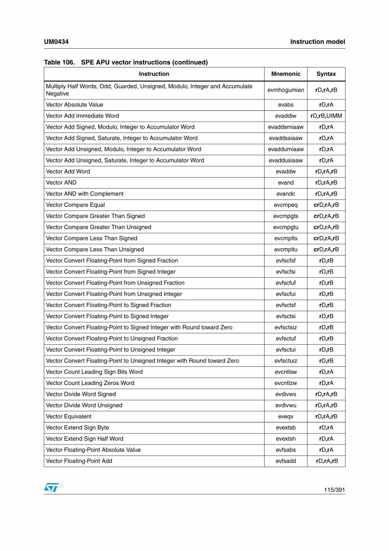
UM0434 Instruction model
115/391
Multiply Half Words, Odd, Guarded, Unsigned, Modulo, Integer and Accumulate Negative
evmhogumian rD,rA,rB
Vector Absolute Value evabs rD,rA
Vector Add Immediate Word evaddiw rD,rB,UIMM
Vector Add Signed, Modulo, Integer to Accumulator Word evaddsmiaaw rD,rA
Vector Add Signed, Saturate, Integer to Accumulator Word evaddssiaaw rD,rA
Vector Add Unsigned, Modulo, Integer to Accumulator Word evaddumiaaw rD,rA
Vector Add Unsigned, Saturate, Integer to Accumulator Word evaddusiaaw rD,rA
Vector Add Word evaddw rD,rA,rB
Vector AND evand rD,rA,rB
Vector AND with Complement evandc rD,rA,rB
Vector Compare Equal evcmpeq crD,rA,rB
Vector Compare Greater Than Signed evcmpgts crD,rA,rB
Vector Compare Greater Than Unsigned evcmpgtu crD,rA,rB
Vector Compare Less Than Signed evcmplts crD,rA,rB
Vector Compare Less Than Unsigned evcmpltu crD,rA,rB
Vector Convert Floating-Point from Signed Fraction evfscfsf rD,rB
Vector Convert Floating-Point from Signed Integer evfscfsi rD,rB
Vector Convert Floating-Point from Unsigned Fraction evfscfuf rD,rB
Vector Convert Floating-Point from Unsigned Integer evfscfui rD,rB
Vector Convert Floating-Point to Signed Fraction evfsctsf rD,rB
Vector Convert Floating-Point to Signed Integer evfsctsi rD,rB
Vector Convert Floating-Point to Signed Integer with Round toward Zero evfsctsiz rD,rB
Vector Convert Floating-Point to Unsigned Fraction evfsctuf rD,rB
Vector Convert Floating-Point to Unsigned Integer evfsctui rD,rB
Vector Convert Floating-Point to Unsigned Integer with Round toward Zero evfsctuiz rD,rB
Vector Count Leading Sign Bits Word evcntlsw rD,rA
Vector Count Leading Zeros Word evcntlzw rD,rA
Vector Divide Word Signed evdivws rD,rA,rB
Vector Divide Word Unsigned evdivwu rD,rA,rB
Vector Equivalent eveqv rD,rA,rB
Vector Extend Sign Byte evextsb rD,rA
Vector Extend Sign Half Word evextsh rD,rA
Vector Floating-Point Absolute Value evfsabs rD,rA
Vector Floating-Point Add evfsadd rD,rA,rB
Table 106. SPE APU vector instructions (continued)
Instruction Mnemonic Syntax
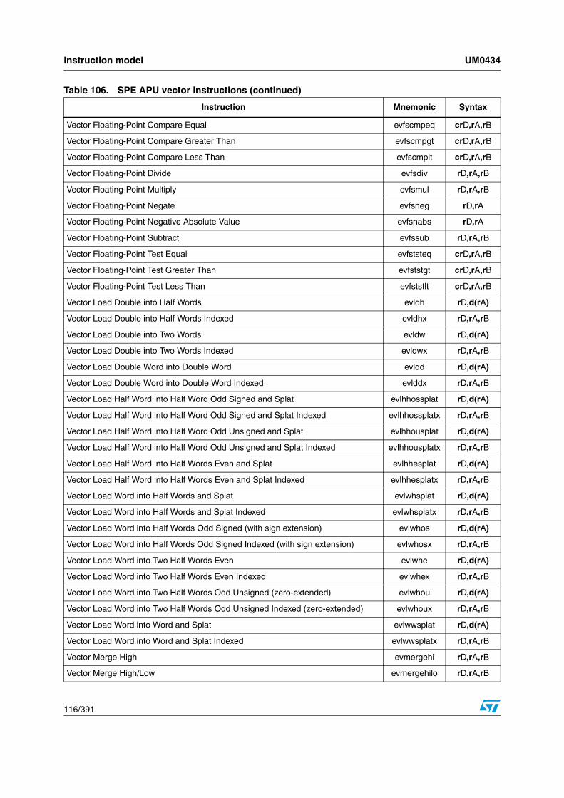
Instruction model UM0434
116/391
Vector Floating-Point Compare Equal evfscmpeq crD,rA,rB
Vector Floating-Point Compare Greater Than evfscmpgt crD,rA,rB
Vector Floating-Point Compare Less Than evfscmplt crD,rA,rB
Vector Floating-Point Divide evfsdiv rD,rA,rB
Vector Floating-Point Multiply evfsmul rD,rA,rB
Vector Floating-Point Negate evfsneg rD,rA
Vector Floating-Point Negative Absolute Value evfsnabs rD,rA
Vector Floating-Point Subtract evfssub rD,rA,rB
Vector Floating-Point Test Equal evfststeq crD,rA,rB
Vector Floating-Point Test Greater Than evfststgt crD,rA,rB
Vector Floating-Point Test Less Than evfststlt crD,rA,rB
Vector Load Double into Half Words evldh rD,d(rA)
Vector Load Double into Half Words Indexed evldhx rD,rA,rB
Vector Load Double into Two Words evldw rD,d(rA)
Vector Load Double into Two Words Indexed evldwx rD,rA,rB
Vector Load Double Word into Double Word evldd rD,d(rA)
Vector Load Double Word into Double Word Indexed evlddx rD,rA,rB
Vector Load Half Word into Half Word Odd Signed and Splat evlhhossplat rD,d(rA)
Vector Load Half Word into Half Word Odd Signed and Splat Indexed evlhhossplatx rD,rA,rB
Vector Load Half Word into Half Word Odd Unsigned and Splat evlhhousplat rD,d(rA)
Vector Load Half Word into Half Word Odd Unsigned and Splat Indexed evlhhousplatx rD,rA,rB
Vector Load Half Word into Half Words Even and Splat evlhhesplat rD,d(rA)
Vector Load Half Word into Half Words Even and Splat Indexed evlhhesplatx rD,rA,rB
Vector Load Word into Half Words and Splat evlwhsplat rD,d(rA)
Vector Load Word into Half Words and Splat Indexed evlwhsplatx rD,rA,rB
Vector Load Word into Half Words Odd Signed (with sign extension) evlwhos rD,d(rA)
Vector Load Word into Half Words Odd Signed Indexed (with sign extension) evlwhosx rD,rA,rB
Vector Load Word into Two Half Words Even evlwhe rD,d(rA)
Vector Load Word into Two Half Words Even Indexed evlwhex rD,rA,rB
Vector Load Word into Two Half Words Odd Unsigned (zero-extended) evlwhou rD,d(rA)
Vector Load Word into Two Half Words Odd Unsigned Indexed (zero-extended) evlwhoux rD,rA,rB
Vector Load Word into Word and Splat evlwwsplat rD,d(rA)
Vector Load Word into Word and Splat Indexed evlwwsplatx rD,rA,rB
Vector Merge High evmergehi rD,rA,rB
Vector Merge High/Low evmergehilo rD,rA,rB
Table 106. SPE APU vector instructions (continued)
Instruction Mnemonic Syntax
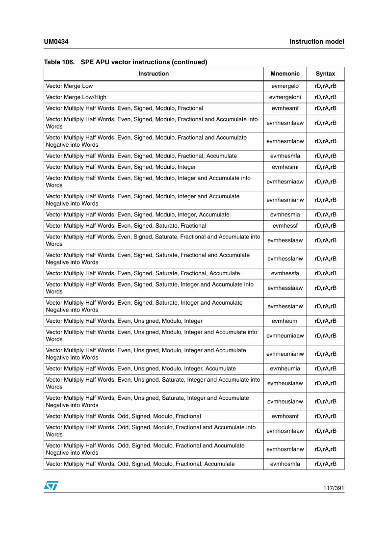
UM0434 Instruction model
117/391
Vector Merge Low evmergelo rD,rA,rB
Vector Merge Low/High evmergelohi rD,rA,rB
Vector Multiply Half Words, Even, Signed, Modulo, Fractional evmhesmf rD,rA,rB
Vector Multiply Half Words, Even, Signed, Modulo, Fractional and Accumulate into Words
evmhesmfaaw rD,rA,rB
Vector Multiply Half Words, Even, Signed, Modulo, Fractional and Accumulate Negative into Words
evmhesmfanw rD,rA,rB
Vector Multiply Half Words, Even, Signed, Modulo, Fractional, Accumulate evmhesmfa rD,rA,rB
Vector Multiply Half Words, Even, Signed, Modulo, Integer evmhesmi rD,rA,rB
Vector Multiply Half Words, Even, Signed, Modulo, Integer and Accumulate into Words
evmhesmiaaw rD,rA,rB
Vector Multiply Half Words, Even, Signed, Modulo, Integer and Accumulate Negative into Words
evmhesmianw rD,rA,rB
Vector Multiply Half Words, Even, Signed, Modulo, Integer, Accumulate evmhesmia rD,rA,rB
Vector Multiply Half Words, Even, Signed, Saturate, Fractional evmhessf rD,rA,rB
Vector Multiply Half Words, Even, Signed, Saturate, Fractional and Accumulate into Words
evmhessfaaw rD,rA,rB
Vector Multiply Half Words, Even, Signed, Saturate, Fractional and Accumulate Negative into Words
evmhessfanw rD,rA,rB
Vector Multiply Half Words, Even, Signed, Saturate, Fractional, Accumulate evmhessfa rD,rA,rB
Vector Multiply Half Words, Even, Signed, Saturate, Integer and Accumulate into Words
evmhessiaaw rD,rA,rB
Vector Multiply Half Words, Even, Signed, Saturate, Integer and Accumulate Negative into Words
evmhessianw rD,rA,rB
Vector Multiply Half Words, Even, Unsigned, Modulo, Integer evmheumi rD,rA,rB
Vector Multiply Half Words, Even, Unsigned, Modulo, Integer and Accumulate into Words
evmheumiaaw rD,rA,rB
Vector Multiply Half Words, Even, Unsigned, Modulo, Integer and Accumulate Negative into Words
evmheumianw rD,rA,rB
Vector Multiply Half Words, Even, Unsigned, Modulo, Integer, Accumulate evmheumia rD,rA,rB
Vector Multiply Half Words, Even, Unsigned, Saturate, Integer and Accumulate into Words
evmheusiaaw rD,rA,rB
Vector Multiply Half Words, Even, Unsigned, Saturate, Integer and Accumulate Negative into Words
evmheusianw rD,rA,rB
Vector Multiply Half Words, Odd, Signed, Modulo, Fractional evmhosmf rD,rA,rB
Vector Multiply Half Words, Odd, Signed, Modulo, Fractional and Accumulate into Words
evmhosmfaaw rD,rA,rB
Vector Multiply Half Words, Odd, Signed, Modulo, Fractional and Accumulate Negative into Words
evmhosmfanw rD,rA,rB
Vector Multiply Half Words, Odd, Signed, Modulo, Fractional, Accumulate evmhosmfa rD,rA,rB
Table 106. SPE APU vector instructions (continued)
Instruction Mnemonic Syntax

Instruction model UM0434
118/391
Vector Multiply Half Words, Odd, Signed, Modulo, Integer evmhosmi rD,rA,rB
Vector Multiply Half Words, Odd, Signed, Modulo, Integer and Accumulate into Words
evmhosmiaaw rD,rA,rB
Vector Multiply Half Words, Odd, Signed, Modulo, Integer and Accumulate Negative into Words
evmhosmianw rD,rA,rB
Vector Multiply Half Words, Odd, Signed, Modulo, Integer, Accumulate evmhosmia rD,rA,rB
Vector Multiply Half Words, Odd, Signed, Saturate, Fractional evmhossf rD,rA,rB
VectoR Multiply Half Words, Odd, Signed, Saturate, Fractional and Accumulate into Words
evmhossfaaw rD,rA,rB
Vector Multiply Half Words, Odd, Signed, Saturate, Fractional and Accumulate Negative into Words
evmhossfanw rD,rA,rB
Vector Multiply Half Words, Odd, Signed, Saturate, Fractional, Accumulate evmhossfa rD,rA,rB
Vector Multiply Half Words, Odd, Signed, Saturate, Integer and Accumulate into Words
evmhossiaaw rD,rA,rB
Vector Multiply Half Words, Odd, Signed, Saturate, Integer and Accumulate Negative into Words
evmhossianw rD,rA,rB
Vector Multiply Half Words, Odd, Unsigned, Modulo, Integer evmhoumi rD,rA,rB
Vector Multiply Half Words, Odd, Unsigned, Modulo, Integer and Accumulate into Words
evmhoumiaaw rD,rA,rB
Vector Multiply Half Words, Odd, Unsigned, Modulo, Integer and Accumulate Negative into Words
evmhoumianw rD,rA,rB
Vector Multiply Half Words, Odd, Unsigned, Modulo, Integer, Accumulate evmhoumia rD,rA,rB
Vector Multiply Half Words, Odd, Unsigned, Saturate, Integer and Accumulate into Words
evmhousiaaw rD,rA,rB
Vector Multiply Half Words, Odd, Unsigned, Saturate, Integer and Accumulate Negative into Words
evmhousianw rD,rA,rB
Vector Multiply Word High Signed, Modulo, Fractional evmwhsmf rD,rA,rB
Vector Multiply Word High Signed, Modulo, Fractional and Accumulate evmwhsmfa rD,rA,rB
Vector Multiply Word High Signed, Modulo, Integer evmwhsmi rD,rA,rB
Vector Multiply Word High Signed, Modulo, Integer and Accumulate evmwhsmia rD,rA,rB
Vector Multiply Word High Signed, Saturate, Fractional evmwhssf rD,rA,rB
Vector Multiply Word High Signed, Saturate, Fractional and Accumulate evmwhssfa rD,rA,rB
Vector Multiply Word High Unsigned, Modulo, Integer evmwhumi rD,rA,rB
Vector Multiply Word High Unsigned, Modulo, Integer and Accumulate evmwhumia rD,rA,rB
Vector Multiply Word Low Signed, Modulo, Integer and Accumulate in Words evmwlsmiaaw rD,rA,rB
Vector Multiply Word Low Signed, Modulo, Integer and Accumulate Negative in Words
evmwlsmianw rD,rA,rB
Vector Multiply Word Low Signed, Saturate, Integer and Accumulate in Words evmwlssiaaw rD,rA,rB
Table 106. SPE APU vector instructions (continued)
Instruction Mnemonic Syntax

UM0434 Instruction model
119/391
Vector Multiply Word Low Signed, Saturate, Integer and Accumulate Negative in Words
evmwlssianw rD,rA,rB
Vector Multiply Word Low Unsigned, Modulo, Integer evmwlsmi rD,rA,rB
Vector Multiply Word Low Unsigned, Modulo, Integer and Accumulate evmwlumia rD,rA,rB
Vector Multiply Word Low Unsigned, Modulo, Integer and Accumulate in Words evmwlumiaaw rD,rA,rB
Vector Multiply Word Low Unsigned, Modulo, Integer and Accumulate Negative in Words
evmwlumianw rD,rA,rB
Vector Multiply Word Low Unsigned, Saturate, Integer and Accumulate in Words evmwlusiaaw rD,rA,rB
Vector Multiply Word Low Unsigned, Saturate, Integer and Accumulate Negative in Words
evmwlusianw rD,rA,rB
Vector Multiply Word Signed, Modulo, Fractional evmwsmf rD,rA,rB
Vector Multiply Word Signed, Modulo, Fractional and Accumulate evmwsmfa rD,rA,rB
Vector Multiply Word Signed, Modulo, Fractional and Accumulate evmwsmfaa rD,rA,rB
Vector Multiply Word Signed, Modulo, Fractional and Accumulate Negative evmwsmfan rD,rA,rB
Vector Multiply Word Signed, Modulo, Integer evmwsmi rD,rA,rB
Vector Multiply Word Signed, Modulo, Integer and Accumulate evmwsmia rD,rA,rB
Vector Multiply Word Signed, Modulo, Integer and Accumulate evmwsmiaa rD,rA,rB
Vector Multiply Word Signed, Modulo, Integer and Accumulate Negative evmwsmian rD,rA,rB
Vector Multiply Word Signed, Saturate, Fractional evmwssf rD,rA,rB
Vector Multiply Word Signed, Saturate, Fractional and Accumulate evmwssfa rD,rA,rB
Vector Multiply Word Signed, Saturate, Fractional and Accumulate evmwssfaa rD,rA,rB
Vector Multiply Word Signed, Saturate, Fractional and Accumulate Negative evmwssfan rD,rA,rB
Vector Multiply Word Unsigned, Modulo, Integer evmwumi rD,rA,rB
Vector Multiply Word Unsigned, Modulo, Integer and Accumulate evmwumia rD,rA,rB
Vector Multiply Word Unsigned, Modulo, Integer and Accumulate evmwumiaa rD,rA,rB
Vector Multiply Word Unsigned, Modulo, Integer and Accumulate Negative evmwumian rD,rA,rB
Vector NAND evnand rD,rA,rB
Vector Negate evneg rD,rA
Vector NOR evnor rD,rA,rB
Vector OR evor rD,rA,rB
Vector OR with Complement evorc rD,rA,rB
Vector Rotate Left Word evrlw rD,rA,rB
Vector Rotate Left Word Immediate evrlwi rD,rA,UIMM
Vector Round Word evrndw rD,rA
Vector Select evsel rD,rA,rB,crS
Vector Shift Left Word evslw rD,rA,rB
Table 106. SPE APU vector instructions (continued)
Instruction Mnemonic Syntax

Instruction model UM0434
120/391
5.10.4 Embedded vector and scalar single precision floating point APU instructions
The vector and scalar SPFP APUs perform floating-point operations on single-precision operands. These operations are IEEE-compliant with software interrupt handlers and offer a simpler interrupt model than the floating-point instructions defined by the PowerPC ISA. Instead of FPRs, these instructions use GPRs and offer improved performance for
Vector Shift Left Word Immediate evslwi rD,rA,UIMM
Vector Shift Right Word Immediate Signed evsrwis rD,rA,UIMM
Vector Shift Right Word Immediate Unsigned evsrwiu rD,rA,UIMM
Vector Shift Right Word Signed evsrws rD,rA,rB
Vector Shift Right Word Unsigned evsrwu rD,rA,rB
Vector Splat Fractional Immediate evsplatfi rD,SIMM
Vector Splat Immediate evsplati rD,SIMM
Vector Store Double of Double evstdd rS,d(rA)
Vector Store Double of Double Indexed evstddx rS,rA,rB
Vector Store Double of Four Half Words evstdh rS,d(rA)
Vector Store Double of Four Half Words Indexed evstdhx rS,rA,rB
Vector Store Double of Two Words evstdw rS,d(rA)
Vector Store Double of Two Words Indexed evstdwx rS,rA,rB
Vector Store Word of Two Half Words from Even evstwhe rS,d(rA)
Vector Store Word of Two Half Words from Even Indexed evstwhex rS,rA,rB
Vector Store Word of Two Half Words from Odd evstwho rS,d(rA)
Vector Store Word of Two Half Words from Odd Indexed evstwhox rS,rA,rB
Vector Store Word of Word from Even evstwwe rS,d(rA)
Vector Store Word of Word from Even Indexed evstwwex rS,rA,rB
Vector Store Word of Word from Odd evstwwo rS,d(rA)
Vector Store Word of Word from Odd Indexed evstwwox rS,rA,rB
Vector Subtract from Word evsubfw rD,rA,rB
Vector Subtract Immediate from Word evsubifw rD,UIMM,rB
Vector Subtract Signed, Modulo, Integer to Accumulator Word evsubfsmiaaw rD,rA
Vector Subtract Signed, Saturate, Integer to Accumulator Word evsubfssiaaw rD,rA
Vector Subtract Unsigned, Modulo, Integer to Accumulator Word evsubfumiaaw rD,rA
Vector Subtract Unsigned, Saturate, Integer to Accumulator Word evsubfusiaaw rD,rA
Vector XOR evxor rD,rA,rB
1. An implementation can restrict the number of bits specified in a mask. The e200z3 limits it to 16 bits, which allows the user to perform bit-reversed address computations for 65536-byte samples.
Table 106. SPE APU vector instructions (continued)
Instruction Mnemonic Syntax

UM0434 Instruction model
121/391
converting between floating-point, integer, and fractional values. Sharing GPRs allows vector floating-point instructions to use SPE load and store instructions.
The two SPFP APUs are described as follows:
● Vector SPFP instructions operate on a vector of two 32-bit, single-precision floating-point numbers that reside in the upper and lower halves of the 64-bit GPRs. These instructions are listed in Table 107 alongside their scalar equivalents.
● Scalar SPFP instructions operate on single 32-bit operands that reside in the lower 32 bits of the GPRs. These instructions are listed in Table 107.
Note: Both the vector and scalar versions of the instructions have the same syntax.
Table 107. Vector and scalar SPFP APU floating-point instructions
InstructionMnemonic
SyntaxScalar Vector
Convert Floating-Point from Signed Fraction efscfsf evfscfsf rD,rB
Convert Floating-Point from Signed Integer efscfsi evfscfsi rD,rB
Convert Floating-Point from Unsigned Fraction efscfuf evfscfuf rD,rB
Convert Floating-Point from Unsigned Integer efscfui evfscfui rD,rB
Convert Floating-Point to Signed Fraction efsctsf evfsctsf rD,rB
Convert Floating-Point to Signed Integer efsctsi evfsctsi rD,rB
Convert Floating-Point to Signed Integer with Round toward Zero efsctsiz evfsctsiz rD,rB
Convert Floating-Point to Unsigned Fraction efsctuf evfsctuf rD,rB
Convert Floating-Point to Unsigned Integer efsctui evfsctui rD,rB
Convert Floating-Point to Unsigned Integer with Round toward Zero efsctuiz evfsctuiz rD,rB
Floating-Point Absolute Value efsabs evfsabs rD,rA
Floating-Point Add efsadd evfsadd rD,rA,rB
Floating-Point Compare Equal efscmpeq evfscmpeq crD,rA,rB
Floating-Point Compare Greater Than efscmpgt evfscmpgt crD,rA,rB
Floating-Point Compare Less Than efscmplt evfscmplt crD,rA,rB
Floating-Point Divide efsdiv evfsdiv rD,rA,rB
Floating-Point Multiply efsmul evfsmul rD,rA,rB
Floating-Point Negate efsneg evfsneg rD,rA
Floating-Point Negative Absolute Value efsnabs evfsnabs rD,rA
Floating-Point Subtract efssub evfssub rD,rA,rB
Floating-Point Test Equal efststeq evfststeq crD,rA,rB
Floating-Point Test Greater Than efststgt evfststgt crD,rA,rB
Floating-Point Test Less Than efststlt evfststlt crD,rA,rB

Instruction model UM0434
122/391
Options for embedded floating-point APU implementations
Table 108 lists implementation options allowed by the embedded floating-point architecture and describes how the e200z3 handles those options.
5.11 Unimplemented SPRs and read only SPRsThe e200z3 fully decodes the SPR field of mfspr and mtspr instructions. If the SPR specified is undefined and not privileged, an illegal instruction exception is generated. If the SPR specified is undefined and privileged and the CPU is in user mode (MSR[PR] = 1), a privileged instruction exception is generated. If the SPR specified is undefined and privileged and the CPU is in supervisor mode (MSR[PR] = 0), an illegal instruction exception is generated.
For mtspr, if the SPR specified is read-only and not privileged, an illegal instruction exception is generated. If the SPR specified is read-only and privileged and the CPU is in user mode (MSR[PR] = 1, a privileged instruction exception is generated. If the SPR specified is read-only and privileged and the CPU is in supervisor mode (MSR[PR] = 0), an illegal instruction exception is generated.
5.12 Invalid instruction formsTable 109 describes invalid instruction forms.
Table 108. Embedded floating-point APU options
Optione200z3
Implementation
Overflow and underflow conditions may be signaled by doing exponent evaluation of the operation. If an examining of the exponents determines that an overflow or underflow could occur, the implementation may choose to signal an overflow or underflow.
Follows the recommendation; does not use the estimation.
If an operand for a calculation or conversion is denormalized, the implementation may choose to use a same-signed zero value in place of the denormalized operand.
Uses a same-signed zero value in place of the denormalized operand.
+Infinity and -Infinity rounding modes are not required to be handled by an implementation. If an implementation does not support ±Infinity rounding modes and the rounding mode is set to be +Infinity or -Infinity, an embedded floating-point round interrupt occurs after every floating-point instruction for which rounding may occur, regardless of the value of FINXE, unless an embedded floating-point data interrupt also occurs and is taken.
Supports rounding to ± Infinity.
For absolute value, negate, and negative absolute value operations, an implementation may choose either to simply perform the sign bit operation recognizing interrupts or to compute the operation and handle exceptions and saturation where appropriate.
A sign bit operation is performed; interrupts are taken.
SPEFSCR FGH and FXH bits are undefined upon the completion of a scalar floating-point operation. An implementation may choose to clear them or leave them unchanged.
Always clears these bits for such operations.
An implementation may choose to only implement sticky bit setting by hardware for FDBZS and FINXS, allowing software to manage the other sticky bits. It is recommended that all future implementations implement all sticky bit settings in hardware.
Implements all sticky bit settings in hardware.

UM0434 Instruction model
123/391
5.13 Instruction summaryIn addition to the SPE instructions listed in Table 106 and the floating-point instructions listed in Table 107, the e200z3 implements the instructions defined in Table 110 and Table 111. Instructions not listed in these tables are not supported by the e200z3 core and signal an illegal, unimplemented, or floating-point unavailable exception. Implementation-dependent instructions are identified with a footnote.
Note: Specific APUs are not included in the table below:● SPE APU
● VLE extension
5.13.1 Instruction index sorted by mnemonic
Table 110 lists instructions by mnemonic.
Table 109. Invalid instruction forms
Instructions Descriptions
Load and store with update
Book E defines as an invalid form the case when a load with update instruction specifies the same register in the rD and rA field of the instruction. For this invalid case, the e200z3 core performs the instruction and updates the register with the load data. In addition, if rA = 0 for any load or store with update instruction, the e200z3 core updates rA (GPR0).
Load Multiple Word (lmw)
Book E defines as invalid any form of lmw instruction in which rA is in the range of registers to be loaded, including the case in which rA = 0. On the e200z3, invalid forms of lmw execute as follows:
– Case 1: rA is in the range of rD, rA ≠ 0. In this case address generation for individual loads to register targets is done using the architectural value of rA which existed when beginning execution of this lmw instruction. rA is overwritten with a value fetched from memory as if it had not been the base register. Note that if the instruction is interrupted and restarted, the base address may be different if rA has been overwritten.
– Case 2: rA = 0 and rD = 0. In this case address generation for all loads to register targets rD = 0 to rD = 31 is done substituting the value of 0 for rA.
Branch Conditional to Count Register [and Link]
Book E defines as invalid any bcctr or bcctrl instruction that specifies the decrement and test CTR (BO[2] = 0) option. The e200z3 executes instructions with these invalid forms by decrementing the CTR and branching to the location specified by the pre-decremented CTR value if all CR and CTR conditions are met as specified by the other BO field settings.
Instructions with non-zero reserved fields
Book E defines certain bit fields in various instructions as reserved and specifies that these fields be set to zero. Following the Book E recommendation, the e200z3 ignores the value of the reserved field (bit 31) in X-form integer load and store instructions. The e200z3 ignores the value of the reserved ‘z’ bits in the BO field of branch instructions. For all other instructions, the e200z3 generates an illegal instruction exception if a reserved field is non-zero.
Table 110. Instructions sorted by mnemonic
Format
Opcode
Mnemonic InstructionPrimary
(Inst0:5)
Extended
(Inst21:31)
X 011111 01000 01010 0 add Add
X 011111 01000 01010 1 add. Add & record CR
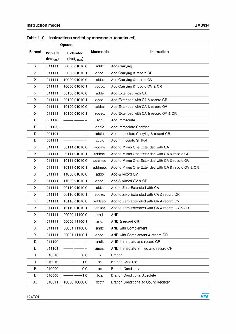
Instruction model UM0434
124/391
X 011111 00000 01010 0 addc Add Carrying
X 011111 00000 01010 1 addc. Add Carrying & record CR
X 011111 10000 01010 0 addco Add Carrying & record OV
X 011111 10000 01010 1 addco. Add Carrying & record OV & CR
X 011111 00100 01010 0 adde Add Extended with CA
X 011111 00100 01010 1 adde. Add Extended with CA & record CR
X 011111 10100 01010 0 addeo Add Extended with CA & record OV
X 011111 10100 01010 1 addeo. Add Extended with CA & record OV & CR
D 001110 ––––– ––––– – addi Add Immediate
D 001100 ––––– ––––– – addic Add Immediate Carrying
D 001101 ––––– ––––– – addic. Add Immediate Carrying & record CR
D 001111 ––––– ––––– – addis Add Immediate Shifted
X 011111 00111 01010 0 addme Add to Minus One Extended with CA
X 011111 00111 01010 1 addme. Add to Minus One Extended with CA & record CR
X 011111 10111 01010 0 addmeo Add to Minus One Extended with CA & record OV
X 011111 10111 01010 1 addmeo. Add to Minus One Extended with CA & record OV & CR
X 011111 11000 01010 0 addo Add & record OV
X 011111 11000 01010 1 addo. Add & record OV & CR
X 011111 00110 01010 0 addze Add to Zero Extended with CA
X 011111 00110 01010 1 addze. Add to Zero Extended with CA & record CR
X 011111 10110 01010 0 addzeo Add to Zero Extended with CA & record OV
X 011111 10110 01010 1 addzeo. Add to Zero Extended with CA & record OV & CR
X 011111 00000 11100 0 and AND
X 011111 00000 11100 1 and. AND & record CR
X 011111 00001 11100 0 andc AND with Complement
X 011111 00001 11100 1 andc. AND with Complement & record CR
D 011100 ––––– ––––– – andi. AND Immediate and record CR
D 011101 ––––– ––––– – andis. AND Immediate Shifted and record CR
I 010010 ––––– ––––0 0 b Branch
I 010010 ––––– ––––1 0 ba Branch Absolute
B 010000 ––––– ––––0 0 bc Branch Conditional
B 010000 ––––– ––––1 0 bca Branch Conditional Absolute
XL 010011 10000 10000 0 bcctr Branch Conditional to Count Register
Table 110. Instructions sorted by mnemonic (continued)
Format
Opcode
Mnemonic InstructionPrimary
(Inst0:5)
Extended
(Inst21:31)

UM0434 Instruction model
125/391
XL 010011 10000 10000 1 bcctrl Branch Conditional to Count Register and Link
B 010000 ––––– ––––0 1 bcl Branch Conditional and Link
B 010000 ––––– ––––1 1 bcla Branch Conditional and Link Absolute
XL 010011 00000 10000 0 bclr Branch Conditional to Link Register
XL 010011 00000 10000 1 bclrl Branch Conditional to Link Register and Link
I 010010 ––––– ––––0 1 bl Branch and Link
I 010010 ––––– ––––1 1 bla Branch and Link Absolute
X 011111 00000 00000 / cmp Compare
D 001011 ––––– ––––– – cmpi Compare Immediate
X 011111 00001 00000 / cmpl Compare Logical
D 001010 ––––– ––––– – cmpli Compare Logical Immediate
X 011111 00000 11010 0 cntlzw Count Leading Zeros Word
X 011111 00000 11010 1 cntlzw. Count Leading Zeros Word and record CR
XL 010011 01000 00001 / crand Condition Register AND
XL 010011 00100 00001 / crandc Condition Register AND with Complement
XL 010011 01001 00001 / creqv Condition Register Equivalent
XL 010011 00111 00001 / crnand Condition Register NAND
XL 010011 00001 00001 / crnor Condition Register NOR
XL 010011 01110 00001 / cror Condition Register OR
XL 010011 01101 00001 / crorc Condition Register OR with Complement
XL 010011 00110 00001 / crxor Condition Register XOR
X 011111 10111 10110 / dcba Data Cache Block Allocate
X 011111 00010 10110 / dcbf Data Cache Block Flush
X 011111 01110 10110 / dcbi Data Cache Block Invalidate
X 011111 00001 10110 / dcbst Data Cache Block Store
X 011111 01000 10110 / dcbt Data Cache Block Touch
X 011111 00111 10110 / dcbtst Data Cache Block Touch for Store
X 011111 11111 10110 / dcbz Data Cache Block set to Zero
X 011111 01111 01011 0 divw Divide Word
X 011111 01111 01011 1 divw. Divide Word and record CR
X 011111 11111 01011 0 divwo Divide Word and record OV
X 011111 11111 01011 1 divwo. Divide Word and record OV and CR
X 011111 01110 01011 0 divwu Divide Word Unsigned
Table 110. Instructions sorted by mnemonic (continued)
Format
Opcode
Mnemonic InstructionPrimary
(Inst0:5)
Extended
(Inst21:31)

Instruction model UM0434
126/391
X 011111 01110 01011 1 divwu. Divide Word Unsigned and record CR
X 011111 11110 01011 0 divwuo Divide Word Unsigned and record OV
X 011111 11110 01011 1 divwuo. Divide Word Unsigned and record OV and CR
X 011111 01000 11100 0 eqv Equivalent
X 011111 01000 11100 1 eqv. Equivalent and record CR
X 011111 11101 11010 0 extsb Extend Sign Byte
X 011111 11101 11010 1 extsb. Extend Sign Byte and record CR
X 011111 11100 11010 0 extsh Extend Sign Half Word
X 011111 11100 11010 1 extsh. Extend Sign Half Word and record CR
X 111111 01000 01000 0 fabs(1) Floating Absolute Value
X 111111 01000 01000 1 fabs.(1) Floating Absolute Value and record CR
A 111111 ––––– 10101 0 fadd1(1) Floating Add
A 111111 ––––– 10101 1 fadd.(1) Floating Add and record CR
A 111011 ––––– 10101 0 fadds(1) Floating Add Single
A 111011 ––––– 10101 1 fadds.(1) Floating Add Single and record CR
X 111111 11010 01110 / fcfid(1) Floating Convert From Int Doubleword
X 111111 00001 00000 / fcmpo(1) Floating Compare Ordered
X 111111 00000 00000 / fcmpu(1) Floating Compare Unordered
X 111111 11001 01110 / fctid(1) Floating Convert To Int Doubleword
X 111111 11001 01111 / fctidz(1) Floating Convert To Int Doubleword with round to Zero
X 111111 00000 01110 0 fctiw(1) Floating Convert To Int Word
X 111111 00000 01110 1 fctiw.(1) Floating Convert To Int Word and record CR
X 111111 00000 01111 0 fctiwz(1) Floating Convert To Int Word with round to Zero
X 111111 00000 01111 1 fctiwz.(1) Floating convert to Int word with round to zero & record CR
A 111111 ––––– 10010 0 fdiv(1) Floating Divide
A 111111 ––––– 10010 1 fdiv.(1) Floating Divide and record CR
A 111011 ––––– 10010 0 fdivs(1) Floating Divide Single
A 111011 ––––– 10010 1 fdivs.(1) Floating Divide Single and record CR
A 111111 ––––– 11101 0 fmadd(1) Floating Multiply-Add
A 111111 ––––– 11101 1 fmadd.(1) Floating Multiply-Add and record CR
A 111011 ––––– 11101 0 fmadds(1) Floating Multiply-Add Single
A 111011 ––––– 11101 1 fmadds.(1) Floating Multiply-Add Single and record CR
X 111111 00010 01000 0 fmr(1) Floating Move Register
Table 110. Instructions sorted by mnemonic (continued)
Format
Opcode
Mnemonic InstructionPrimary
(Inst0:5)
Extended
(Inst21:31)

UM0434 Instruction model
127/391
X 111111 00010 01000 1 fmr.(1) Floating Move Register and record CR
A 111111 ––––– 11100 0 fmsub(1) Floating Multiply-Subtract
A 111111 ––––– 11100 1 fmsub.(1) Floating Multiply-Subtract and record CR
A 111011 ––––– 11100 0 fmsubs(1) Floating Multiply-Subtract Single
A 111011 ––––– 11100 1 fmsubs.(1) Floating Multiply-Subtract Single and record CR
A 111111 ––––– 11001 0 fmul(1) Floating Multiply
A 111111 ––––– 11001 1 fmul.(1) Floating Multiply and record CR
A 111011 ––––– 11001 0 fmuls(1) Floating Multiply Single
A 111011 ––––– 11001 1 fmuls.(1) Floating Multiply Single and record CR
X 111111 00100 01000 0 fnabs(1) Floating Negative Absolute Value
X 111111 00100 01000 1 fnabs.(1) Floating Negative Absolute Value and record CR
X 111111 00001 01000 0 fneg(1) Floating Negate
X 111111 00001 01000 1 fneg.(1) Floating Negate and record CR
A 111111 ––––– 11111 0 fnmadd(1) Floating Negative Multiply-Add
A 111111 ––––– 11111 1 fnmadd.(1) Floating Negative Multiply-Add and record CR
A 111011 ––––– 11111 0 fnmadds(1) Floating Negative Multiply-Add Single
A 111011 ––––– 11111 1 fnmadds(1) Floating Negative Multiply-Add Single and record CR
A 111111 ––––– 11110 0 fnmsub(1) Floating Negative Multiply-Subtract
A 111111 ––––– 11110 1 fnmsub.(1) Floating Negative Multiply-Subtract and record CR
A 111011 ––––– 11110 0 fnmsubs(1) Floating Negative Multiply-Subtract Single
A 111011 ––––– 11110 1 fnmsubs(1) Floating Negative Multiply-Subtract Single and record CR
A 111011 ––––– 11000 0 fres(1) Floating Reciprocal Estimate Single
A 111011 ––––– 11000 1 fres.(1) Floating Reciprocal Estimate Single and record CR
X 111111 00000 01100 0 frsp(1) Floating Round to Single-Precision
X 111111 00000 01100 1 frsp.(1) Floating Round to Single-Precision and record CR
A 111111 ––––– 11010 0 frsqrte(1) Floating Reciprocal Square Root Estimate
A 111111 ––––– 11010 1 frsqrte.(1) Floating Reciprocal Square Root Estimate and record CR
A 111111 ––––– 10111 0 fsel(1) Floating Select
A 111111 ––––– 10111 1 fsel.(1) Floating Select and record CR
A 111111 ––––– 10110 0 fsqrt(1) Floating Square Root
A 111111 ––––– 10110 1 fsqrt.(1) Floating Square Root and record CR
A 111011 ––––– 10110 0 fsqrts(1) Floating Square Root Single
A 111011 ––––– 10110 1 fsqrts.(1) Floating Square Root Single and record CR
Table 110. Instructions sorted by mnemonic (continued)
Format
Opcode
Mnemonic InstructionPrimary
(Inst0:5)
Extended
(Inst21:31)

Instruction model UM0434
128/391
A 111111 ––––– 10100 0 fsub(1) Floating Subtract
A 111111 ––––– 10100 1 fsub.(1) Floating Subtract and record CR
A 111011 ––––– 10100 0 fsubs(1) Floating Subtract Single
A 111011 ––––– 10100 1 fsubs.(1) Floating Subtract Single and record CR
X 011111 11110 10110 / icbi Instruction Cache Block Invalidate
X 011111 00000 10110 / icbt Instruction Cache Block Touch
X 011111 ––––– 01111 / isel (2) Integer Select
XL 010011 00100 10110 / isync Instruction Synchronize
D 100010 ––––– ––––– – lbz Load Byte and Zero
D 100011 ––––– ––––– – lbzu Load Byte and Zero with Update
X 011111 00011 10111 / lbzux Load Byte and Zero with Update Indexed
X 011111 00010 10111 / lbzx Load Byte and Zero Indexed
D 110010 ––––– ––––– – lfd (1) Load Floating-Point Double
D 110011 ––––– ––––– – lfdu (1) Load Floating-Point Double with Update
X 011111 10011 10111 / lfdux (1) Load Floating-Point Double with Update Indexed
X 011111 10010 10111 / lfdx (1) Load Floating-Point Double Indexed
D 110000 ––––– ––––– – lfs (1) Load Floating-Point Single
D 110001 ––––– ––––– – lfsu (1) Load Floating-Point Single with Update
X 011111 10001 10111 / lfsux (1) Load Floating-Point Single with Update Indexed
X 011111 10000 10111 / lfsx (1) Load Floating-Point Single Indexed
D 101010 ––––– ––––– – lha Load Half Word Algebraic
D 101011 ––––– ––––– – lhau Load Half Word Algebraic with Update
X 011111 01011 10111 / lhaux Load Half Word Algebraic with Update Indexed
X 011111 01010 10111 / lhax Load Half Word Algebraic Indexed
X 011111 11000 10110 / lhbrx Load Half Word Byte-Reverse Indexed
D 101000 ––––– ––––– – lhz Load Half Word and Zero
D 101001 ––––– ––––– – lhzu Load Half Word and Zero with Update
X 011111 01001 10111 / lhzux Load Half Word and Zero with Update Indexed
X 011111 01000 10111 / lhzx Load Half Word and Zero Indexed
D 101110 ––––– ––––– – lmw Load Multiple Word
X 011111 10010 10101 / lswi(3) Load String Word Immediate
X 011111 10000 10101 / lswx(3) Load String Word Indexed
X 011111 00000 10100 / lwarx(4) Load Word and Reserve Indexed
Table 110. Instructions sorted by mnemonic (continued)
Format
Opcode
Mnemonic InstructionPrimary
(Inst0:5)
Extended
(Inst21:31)

UM0434 Instruction model
129/391
X 011111 10000 10110 / lwbrx Load Word Byte-Reverse Indexed
D 100000 ––––– ––––– – lwz Load Word and Zero
D 100001 ––––– ––––– – lwzu Load Word and Zero with Update
X 011111 00001 10111 / lwzux Load Word and Zero with Update Indexed
X 011111 00000 10111 / lwzx Load Word and Zero Indexed
X 011111 11010 10110 / mbar(4) Memory Barrier
XL 010011 00000 00000 / mcrf Move Condition Register Field
X 111111 00010 00000 / mcrfs(1) Move to Condition Register from FPSCR
X 011111 10000 00000 / mcrxr Move to Condition Register from XER
X 011111 01000 10011 / mfapidi3 Move From APID Indirect
X 011111 00000 10011 / mfcr Move From Condition Register
XFX 011111 01010 00011 / mfdcr(3) Move From Device Control Register
X 011111 01000 00011 / mfdcrx(3) Move From Device Control Register Indexed
X 111111 10010 00111 0 mffs(1) Move From FPSCR
X 111111 10010 00111 1 mffs.(1) Move From FPSCR and record CR
X 011111 00010 10011 / mfmsr Move From Machine State Register
XFX 011111 01010 10011 / mfspr Move From Special Purpose Register
X 011111 10010 10110 / msync(4) Memory Synchronize
XFX 011111 00100 10000 / mtcrf Move To Condition Register Fields
XFX 011111 01110 00011 / mtdcr(3) Move To Device Control Register
X 011111 01100 00011 / mtdcrx(3) Move To Device Control Register Indexed
X 111111 00010 00110 0 mtfsb0(1) Move To FPSCR Bit 0
X 111111 00010 00110 1 mtfsb0.(1) Move To FPSCR Bit 0 and record CR
X 111111 00001 00110 0 mtfsb1(1) Move To FPSCR Bit 1
X 111111 00001 00110 1 mtfsb1.(1) Move To FPSCR Bit 1 and record CR
XFL 111111 10110 00111 0 mtfsf(1) Move To FPSCR Fields
XFL 111111 10110 00111 1 mtfsf.(1) Move To FPSCR Fields and record CR
X 111111 00100 00110 0 mtfsfi(1) Move To FPSCR Field Immediate
X 111111 00100 00110 1 mtfsfi.(1) Move To FPSCR Field Immediate and record CR
X 011111 00100 10010 / mtmsr Move To Machine State Register
XFX 011111 01110 10011 / mtspr Move To Special Purpose Register
X 011111 /0010 01011 0 mulhw Multiply High Word
X 011111 /0010 01011 1 mulhw. Multiply High Word and record CR
Table 110. Instructions sorted by mnemonic (continued)
Format
Opcode
Mnemonic InstructionPrimary
(Inst0:5)
Extended
(Inst21:31)

Instruction model UM0434
130/391
X 011111 /0000 01011 0 mulhwu Multiply High Word Unsigned
X 011111 /0000 01011 1 mulhwu. Multiply High Word Unsigned and record CR
D 000111 ––––– ––––– – mulli Multiply Low Immediate
X 011111 00111 01011 0 mullw Multiply Low Word
X 011111 00111 01011 1 mullw. Multiply Low Word and record CR
X 011111 10111 01011 0 mullwo Multiply Low Word and record OV
X 011111 10111 01011 1 mullwo. Multiply Low Word and record OV and CR
X 011111 01110 11100 0 nand NAND
X 011111 01110 11100 1 nand. NAND and record CR
X 011111 00011 01000 0 neg Negate
X 011111 00011 01000 1 neg. Negate and record CR
X 011111 10011 01000 0 nego Negate and record OV
X 011111 10011 01000 1 nego. Negate and record OV and record CR
X 011111 00011 11100 0 nor NOR
X 011111 00011 11100 1 nor. NOR and record CR
X 011111 01101 11100 0 or OR
X 011111 01101 11100 1 or. OR and record CR
X 011111 01100 11100 0 orc OR with Complement
X 011111 01100 11100 1 orc. OR with Complement and record CR
D 011000 ––––– ––––– – ori OR Immediate
D 011001 ––––– ––––– – oris OR Immediate Shifted
XL 010011 00001 10011 / rfci Return From Critical Interrupt
XL 010011 00001 00111 / rfdi(5) Return From Debug Interrupt
XL 010011 00001 10010 / rfi Return From Interrupt
M 010100 ––––– ––––– 0 rlwimi Rotate Left Word Immed then Mask Insert
M 010100 ––––– ––––– 1 rlwimi. Rotate Left Word Immed then Mask Insert and record CR
M 010101 ––––– ––––– 0 rlwinm Rotate Left Word Immed then AND with Mask
M 010101 ––––– ––––– 1 rlwinm. Rotate left word Immed then AND with Mask & record CR
M 010111 ––––– ––––– 0 rlwnm Rotate Left Word then AND with Mask
M 010111 ––––– ––––– 1 rlwnm. Rotate Left Word then AND with Mask and record CR
SC 010001 / / / / / / / / /1 / sc System Call
X 011111 00000 11000 0 slw Shift Left Word
X 011111 00000 11000 1 slw. Shift Left Word and record CR
Table 110. Instructions sorted by mnemonic (continued)
Format
Opcode
Mnemonic InstructionPrimary
(Inst0:5)
Extended
(Inst21:31)
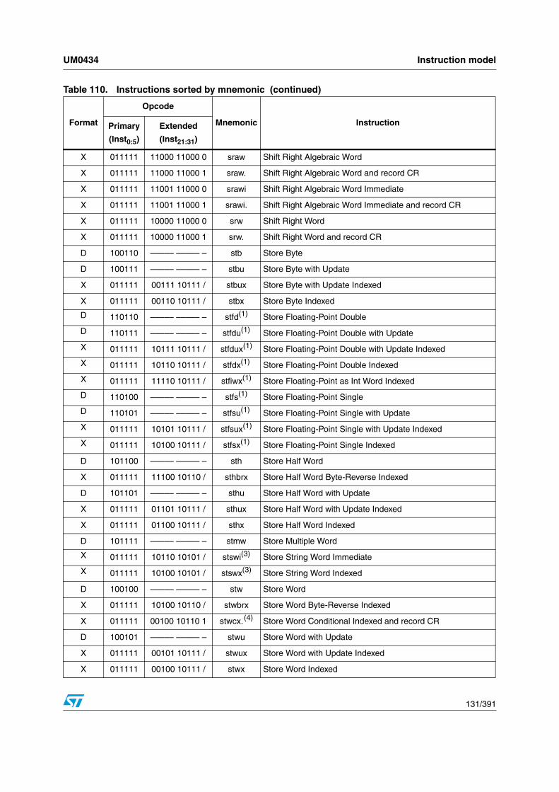
UM0434 Instruction model
131/391
X 011111 11000 11000 0 sraw Shift Right Algebraic Word
X 011111 11000 11000 1 sraw. Shift Right Algebraic Word and record CR
X 011111 11001 11000 0 srawi Shift Right Algebraic Word Immediate
X 011111 11001 11000 1 srawi. Shift Right Algebraic Word Immediate and record CR
X 011111 10000 11000 0 srw Shift Right Word
X 011111 10000 11000 1 srw. Shift Right Word and record CR
D 100110 ––––– ––––– – stb Store Byte
D 100111 ––––– ––––– – stbu Store Byte with Update
X 011111 00111 10111 / stbux Store Byte with Update Indexed
X 011111 00110 10111 / stbx Store Byte Indexed
D 110110 ––––– ––––– – stfd(1) Store Floating-Point Double
D 110111 ––––– ––––– – stfdu(1) Store Floating-Point Double with Update
X 011111 10111 10111 / stfdux(1) Store Floating-Point Double with Update Indexed
X 011111 10110 10111 / stfdx(1) Store Floating-Point Double Indexed
X 011111 11110 10111 / stfiwx(1) Store Floating-Point as Int Word Indexed
D 110100 ––––– ––––– – stfs(1) Store Floating-Point Single
D 110101 ––––– ––––– – stfsu(1) Store Floating-Point Single with Update
X 011111 10101 10111 / stfsux(1) Store Floating-Point Single with Update Indexed
X 011111 10100 10111 / stfsx(1) Store Floating-Point Single Indexed
D 101100 ––––– ––––– – sth Store Half Word
X 011111 11100 10110 / sthbrx Store Half Word Byte-Reverse Indexed
D 101101 ––––– ––––– – sthu Store Half Word with Update
X 011111 01101 10111 / sthux Store Half Word with Update Indexed
X 011111 01100 10111 / sthx Store Half Word Indexed
D 101111 ––––– ––––– – stmw Store Multiple Word
X 011111 10110 10101 / stswi(3) Store String Word Immediate
X 011111 10100 10101 / stswx(3) Store String Word Indexed
D 100100 ––––– ––––– – stw Store Word
X 011111 10100 10110 / stwbrx Store Word Byte-Reverse Indexed
X 011111 00100 10110 1 stwcx.(4) Store Word Conditional Indexed and record CR
D 100101 ––––– ––––– – stwu Store Word with Update
X 011111 00101 10111 / stwux Store Word with Update Indexed
X 011111 00100 10111 / stwx Store Word Indexed
Table 110. Instructions sorted by mnemonic (continued)
Format
Opcode
Mnemonic InstructionPrimary
(Inst0:5)
Extended
(Inst21:31)
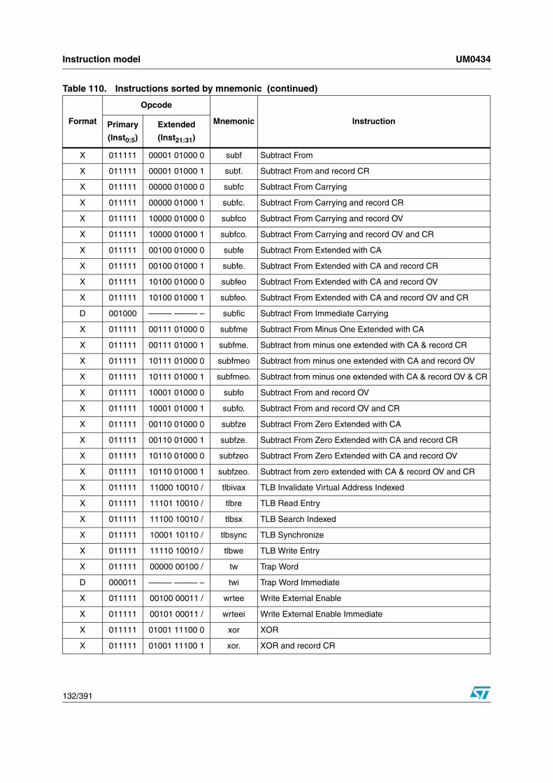
Instruction model UM0434
132/391
X 011111 00001 01000 0 subf Subtract From
X 011111 00001 01000 1 subf. Subtract From and record CR
X 011111 00000 01000 0 subfc Subtract From Carrying
X 011111 00000 01000 1 subfc. Subtract From Carrying and record CR
X 011111 10000 01000 0 subfco Subtract From Carrying and record OV
X 011111 10000 01000 1 subfco. Subtract From Carrying and record OV and CR
X 011111 00100 01000 0 subfe Subtract From Extended with CA
X 011111 00100 01000 1 subfe. Subtract From Extended with CA and record CR
X 011111 10100 01000 0 subfeo Subtract From Extended with CA and record OV
X 011111 10100 01000 1 subfeo. Subtract From Extended with CA and record OV and CR
D 001000 ––––– ––––– – subfic Subtract From Immediate Carrying
X 011111 00111 01000 0 subfme Subtract From Minus One Extended with CA
X 011111 00111 01000 1 subfme. Subtract from minus one extended with CA & record CR
X 011111 10111 01000 0 subfmeo Subtract from minus one extended with CA and record OV
X 011111 10111 01000 1 subfmeo. Subtract from minus one extended with CA & record OV & CR
X 011111 10001 01000 0 subfo Subtract From and record OV
X 011111 10001 01000 1 subfo. Subtract From and record OV and CR
X 011111 00110 01000 0 subfze Subtract From Zero Extended with CA
X 011111 00110 01000 1 subfze. Subtract From Zero Extended with CA and record CR
X 011111 10110 01000 0 subfzeo Subtract From Zero Extended with CA and record OV
X 011111 10110 01000 1 subfzeo. Subtract from zero extended with CA & record OV and CR
X 011111 11000 10010 / tlbivax TLB Invalidate Virtual Address Indexed
X 011111 11101 10010 / tlbre TLB Read Entry
X 011111 11100 10010 / tlbsx TLB Search Indexed
X 011111 10001 10110 / tlbsync TLB Synchronize
X 011111 11110 10010 / tlbwe TLB Write Entry
X 011111 00000 00100 / tw Trap Word
D 000011 ––––– ––––– – twi Trap Word Immediate
X 011111 00100 00011 / wrtee Write External Enable
X 011111 00101 00011 / wrteei Write External Enable Immediate
X 011111 01001 11100 0 xor XOR
X 011111 01001 11100 1 xor. XOR and record CR
Table 110. Instructions sorted by mnemonic (continued)
Format
Opcode
Mnemonic InstructionPrimary
(Inst0:5)
Extended
(Inst21:31)
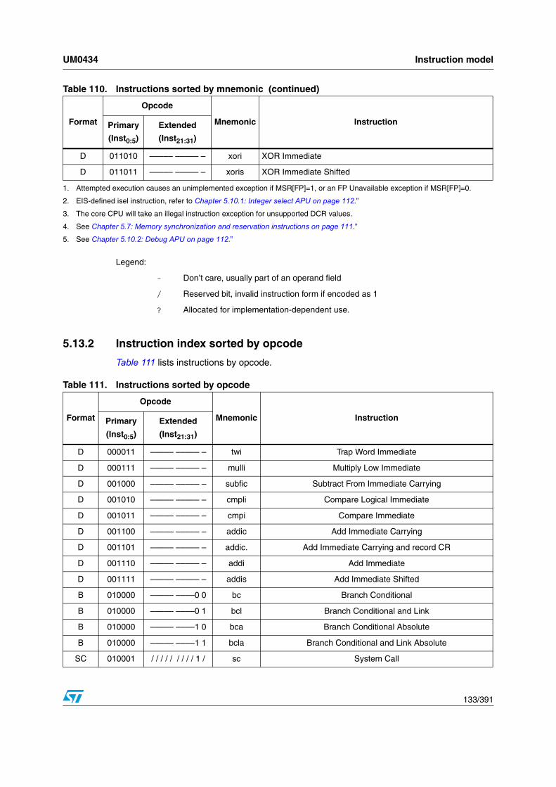
UM0434 Instruction model
133/391
5.13.2 Instruction index sorted by opcode
Table 111 lists instructions by opcode.
D 011010 ––––– ––––– – xori XOR Immediate
D 011011 ––––– ––––– – xoris XOR Immediate Shifted
1. Attempted execution causes an unimplemented exception if MSR[FP]=1, or an FP Unavailable exception if MSR[FP]=0.
2. EIS-defined isel instruction, refer to Chapter 5.10.1: Integer select APU on page 112.”
3. The core CPU will take an illegal instruction exception for unsupported DCR values.
4. See Chapter 5.7: Memory synchronization and reservation instructions on page 111.”
5. See Chapter 5.10.2: Debug APU on page 112.”
Table 110. Instructions sorted by mnemonic (continued)
Format
Opcode
Mnemonic InstructionPrimary
(Inst0:5)
Extended
(Inst21:31)
Legend:
- Don’t care, usually part of an operand field
/ Reserved bit, invalid instruction form if encoded as 1
? Allocated for implementation-dependent use.
Table 111. Instructions sorted by opcode
Format
Opcode
Mnemonic InstructionPrimary
(Inst0:5)
Extended
(Inst21:31)
D 000011 ––––– ––––– – twi Trap Word Immediate
D 000111 ––––– ––––– – mulli Multiply Low Immediate
D 001000 ––––– ––––– – subfic Subtract From Immediate Carrying
D 001010 ––––– ––––– – cmpli Compare Logical Immediate
D 001011 ––––– ––––– – cmpi Compare Immediate
D 001100 ––––– ––––– – addic Add Immediate Carrying
D 001101 ––––– ––––– – addic. Add Immediate Carrying and record CR
D 001110 ––––– ––––– – addi Add Immediate
D 001111 ––––– ––––– – addis Add Immediate Shifted
B 010000 ––––– ––––0 0 bc Branch Conditional
B 010000 ––––– ––––0 1 bcl Branch Conditional and Link
B 010000 ––––– ––––1 0 bca Branch Conditional Absolute
B 010000 ––––– ––––1 1 bcla Branch Conditional and Link Absolute
SC 010001 / / / / / / / / / 1 / sc System Call

Instruction model UM0434
134/391
I 010010 ––––– ––––0 0 b Branch
I 010010 ––––– ––––0 1 bl Branch and Link
I 010010 ––––– ––––1 0 ba Branch Absolute
I 010010 ––––– ––––1 1 bla Branch and Link Absolute
XL 010011 00000 00000 / mcrf Move Condition Register Field
XL 010011 00000 10000 0 bclr Branch Conditional to Link Register
XL 010011 00000 10000 1 bclrl Branch Conditional to Link Register and Link
XL 010011 00001 00001 / crnor Condition Register NOR
XL 010011 00001 00111 / rfdi Return From Debug Interrupt
XL 010011 00001 10010 / rfi Return From Interrupt
XL 010011 00001 10011 / rfci Return From Critical Interrupt
XL 010011 00100 00001 / crandc Condition Register AND with Complement
XL 010011 00100 10110 / isync Instruction Synchronize
XL 010011 00110 00001 / crxor Condition Register XOR
XL 010011 00111 00001 / crnand Condition Register NAND
XL 010011 01000 00001 / crand Condition Register AND
XL 010011 01001 00001 / creqv Condition Register Equivalent
XL 010011 01101 00001 / crorc Condition Register OR with Complement
XL 010011 01110 00001 / cror Condition Register OR
XL 010011 10000 10000 0 bcctr Branch Conditional to Count Register
XL 010011 10000 10000 1 bcctrl Branch Conditional to Count Register and Link
M 010100 ––––– ––––– 0 rlwimi Rotate Left Word Immed then Mask Insert
M 010100 ––––– ––––– 1 rlwimi. Rotate Left Word Immed then Mask Insert and record CR
M 010101 ––––– ––––– 0 rlwinm Rotate Left Word Immed then AND with Mask
M 010101 ––––– ––––– 1 rlwinm. Rotate Left Word Immed then AND with Mask and record CR
M 010111 ––––– ––––– 0 rlwnm Rotate Left Word then AND with Mask
M 010111 ––––– ––––– 1 rlwnm. Rotate Left Word then AND with Mask and record CR
D 011000 ––––– ––––– – ori OR Immediate
D 011001 ––––– ––––– – oris OR Immediate Shifted
D 011010 ––––– ––––– – xori XOR Immediate
D 011011 ––––– ––––– – xoris XOR Immediate Shifted
D 011100 ––––– ––––– – andi. AND Immediate and record CR
D 011101 ––––– ––––– – andis. AND Immediate Shifted and record CR
Table 111. Instructions sorted by opcode (continued)
Format
Opcode
Mnemonic InstructionPrimary
(Inst0:5)
Extended
(Inst21:31)

UM0434 Instruction model
135/391
?? 011111 ––––– 01111 / isel Integer Select
X 011111 00000 00000 / cmp Compare
X 011111 00000 00100 / tw Trap Word
X 011111 00000 01000 0 subfc Subtract From Carrying
X 011111 00000 01000 1 subfc. Subtract From Carrying and record CR
X 011111 00000 01010 0 addc Add Carrying
X 011111 00000 01010 1 addc. Add Carrying and record CR
X 011111 /0000 01011 0 mulhwu Multiply High Word Unsigned
X 011111 /0000 01011 1 mulhwu. Multiply High Word Unsigned and record CR
X 011111 00000 10011 / mfcr Move From Condition Register
X 011111 00000 10100 / lwarx Load Word and Reserve Indexed
X 011111 00000 10110 / icbt Instruction Cache Block Touch
X 011111 00000 10111 / lwzx Load Word and Zero Indexed
X 011111 00000 11000 0 slw Shift Left Word
X 011111 00000 11000 1 slw. Shift Left Word and record CR
X 011111 00000 11010 0 cntlzw Count Leading Zeros Word
X 011111 00000 11010 1 cntlzw. Count Leading Zeros Word and record CR
X 011111 00000 11100 0 and AND
X 011111 00000 11100 1 and. AND and record CR
X 011111 00001 00000 / cmpl Compare Logical
X 011111 00001 01000 0 subf Subtract From
X 011111 00001 01000 1 subf. Subtract From and record CR
X 011111 00001 10110 / dcbst Data Cache Block Store
X 011111 00001 10111 / lwzux Load Word and Zero with Update Indexed
X 011111 00001 11100 0 andc AND with Complement
X 011111 00001 11100 1 andc. AND with Complement and record CR
X 011111 /0010 01011 0 mulhw Multiply High Word
X 011111 /0010 01011 1 mulhw. Multiply High Word and record CR
X 011111 00010 10011 / mfmsr Move From Machine State Register
X 011111 00010 10110 / dcbf Data Cache Block Flush
X 011111 00010 10111 / lbzx Load Byte and Zero Indexed
X 011111 00011 01000 0 neg Negate
X 011111 00011 01000 1 neg. Negate and record CR
Table 111. Instructions sorted by opcode (continued)
Format
Opcode
Mnemonic InstructionPrimary
(Inst0:5)
Extended
(Inst21:31)

Instruction model UM0434
136/391
X 011111 00011 10111 / lbzux Load Byte and Zero with Update Indexed
X 011111 00011 11100 0 nor NOR
X 011111 00011 11100 1 nor. NOR and record CR
X 011111 00100 00011 / wrtee Write External Enable
X 011111 00100 01000 0 subfe Subtract From Extended with CA
X 011111 00100 01000 1 subfe. Subtract From Extended with CA and record CR
X 011111 00100 01010 0 adde Add Extended with CA
X 011111 00100 01010 1 adde. Add Extended with CA and record CR
XFX 011111 00100 10000 / mtcrf Move To Condition Register Fields
X 011111 00100 10010 / mtmsr Move To Machine State Register
X 011111 00100 10110 1 stwcx. Store Word Conditional Indexed and record CR
X 011111 00100 10111 / stwx Store Word Indexed
X 011111 00101 00011 / wrteei Write External Enable Immediate
X 011111 00101 10111 / stwux Store Word with Update Indexed
X 011111 00110 01000 0 subfze Subtract From Zero Extended with CA
X 011111 00110 01000 1 subfze. Subtract From Zero Extended with CA and record CR
X 011111 00110 01010 0 addze Add to Zero Extended with CA
X 011111 00110 01010 1 addze. Add to Zero Extended with CA and record CR
X 011111 00110 10111 / stbx Store Byte Indexed
X 011111 00111 01000 0 subfme Subtract From Minus One Extended with CA
X 011111 00111 01000 1 subfme. Subtract From Minus One Extended with CA and record CR
X 011111 00111 01010 0 addme Add to Minus One Extended with CA
X 011111 00111 01010 1 addme. Add to Minus One Extended with CA and record CR
X 011111 00111 01011 0 mullw Multiply Low Word
X 011111 00111 01011 1 mullw. Multiply Low Word and record CR
X 011111 00111 10110 / dcbtst Data Cache Block Touch for Store
X 011111 00111 10111 / stbux Store Byte with Update Indexed
X 011111 01000 00011 / mfdcrx Move From Device Control Register Indexed
X 011111 01000 01010 0 add Add
X 011111 01000 01010 1 add. Add and record CR
X 011111 01000 10011 / mfapidi Move From APID Indirect
X 011111 01000 10110 / dcbt Data Cache Block Touch
X 011111 01000 10111 / lhzx Load Halfword and Zero Indexed
Table 111. Instructions sorted by opcode (continued)
Format
Opcode
Mnemonic InstructionPrimary
(Inst0:5)
Extended
(Inst21:31)
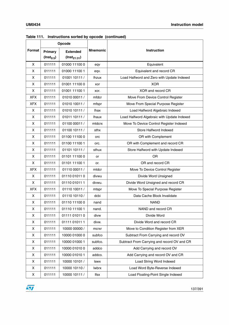
UM0434 Instruction model
137/391
X 011111 01000 11100 0 eqv Equivalent
X 011111 01000 11100 1 eqv. Equivalent and record CR
X 011111 01001 10111 / lhzux Load Halfword and Zero with Update Indexed
X 011111 01001 11100 0 xor XOR
X 011111 01001 11100 1 xor. XOR and record CR
XFX 011111 01010 00011 / mfdcr Move From Device Control Register
XFX 011111 01010 10011 / mfspr Move From Special Purpose Register
X 011111 01010 10111 / lhax Load Halfword Algebraic Indexed
X 011111 01011 10111 / lhaux Load Halfword Algebraic with Update Indexed
X 011111 01100 00011 / mtdcrx Move To Device Control Register Indexed
X 011111 01100 10111 / sthx Store Halfword Indexed
X 011111 01100 11100 0 orc OR with Complement
X 011111 01100 11100 1 orc. OR with Complement and record CR
X 011111 01101 10111 / sthux Store Halfword with Update Indexed
X 011111 01101 11100 0 or OR
X 011111 01101 11100 1 or. OR and record CR
XFX 011111 01110 00011 / mtdcr Move To Device Control Register
X 011111 01110 01011 0 divwu Divide Word Unsigned
X 011111 01110 01011 1 divwu. Divide Word Unsigned and record CR
XFX 011111 01110 10011 / mtspr Move To Special Purpose Register
X 011111 01110 10110 / dcbi Data Cache Block Invalidate
X 011111 01110 11100 0 nand NAND
X 011111 01110 11100 1 nand. NAND and record CR
X 011111 01111 01011 0 divw Divide Word
X 011111 01111 01011 1 divw. Divide Word and record CR
X 011111 10000 00000 / mcrxr Move to Condition Register from XER
X 011111 10000 01000 0 subfco Subtract From Carrying and record OV
X 011111 10000 01000 1 subfco. Subtract From Carrying and record OV and CR
X 011111 10000 01010 0 addco Add Carrying and record OV
X 011111 10000 01010 1 addco. Add Carrying and record OV and CR
X 011111 10000 10101 / lswx Load String Word Indexed
X 011111 10000 10110 / lwbrx Load Word Byte-Reverse Indexed
X 011111 10000 10111 / lfsx Load Floating-Point Single Indexed
Table 111. Instructions sorted by opcode (continued)
Format
Opcode
Mnemonic InstructionPrimary
(Inst0:5)
Extended
(Inst21:31)
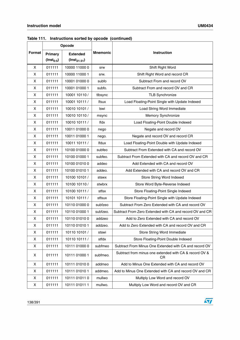
Instruction model UM0434
138/391
X 011111 10000 11000 0 srw Shift Right Word
X 011111 10000 11000 1 srw. Shift Right Word and record CR
X 011111 10001 01000 0 subfo Subtract From and record OV
X 011111 10001 01000 1 subfo. Subtract From and record OV and CR
X 011111 10001 10110 / tlbsync TLB Synchronize
X 011111 10001 10111 / lfsux Load Floating-Point Single with Update Indexed
X 011111 10010 10101 / lswi Load String Word Immediate
X 011111 10010 10110 / msync Memory Synchronize
X 011111 10010 10111 / lfdx Load Floating-Point Double Indexed
X 011111 10011 01000 0 nego Negate and record OV
X 011111 10011 01000 1 nego. Negate and record OV and record CR
X 011111 10011 10111 / lfdux Load Floating-Point Double with Update Indexed
X 011111 10100 01000 0 subfeo Subtract From Extended with CA and record OV
X 011111 10100 01000 1 subfeo. Subtract From Extended with CA and record OV and CR
X 011111 10100 01010 0 addeo Add Extended with CA and record OV
X 011111 10100 01010 1 addeo. Add Extended with CA and record OV and CR
X 011111 10100 10101 / stswx Store String Word Indexed
X 011111 10100 10110 / stwbrx Store Word Byte-Reverse Indexed
X 011111 10100 10111 / stfsx Store Floating-Point Single Indexed
X 011111 10101 10111 / stfsux Store Floating-Point Single with Update Indexed
X 011111 10110 01000 0 subfzeo Subtract From Zero Extended with CA and record OV
X 011111 10110 01000 1 subfzeo. Subtract From Zero Extended with CA and record OV and CR
X 011111 10110 01010 0 addzeo Add to Zero Extended with CA and record OV
X 011111 10110 01010 1 addzeo. Add to Zero Extended with CA and record OV and CR
X 011111 10110 10101 / stswi Store String Word Immediate
X 011111 10110 10111 / stfdx Store Floating-Point Double Indexed
X 011111 10111 01000 0 subfmeo Subtract From Minus One Extended with CA and record OV
X 011111 10111 01000 1 subfmeo.Subtract from minus one extended with CA & record OV &
CR
X 011111 10111 01010 0 addmeo Add to Minus One Extended with CA and record OV
X 011111 10111 01010 1 addmeo. Add to Minus One Extended with CA and record OV and CR
X 011111 10111 01011 0 mullwo Multiply Low Word and record OV
X 011111 10111 01011 1 mullwo. Multiply Low Word and record OV and CR
Table 111. Instructions sorted by opcode (continued)
Format
Opcode
Mnemonic InstructionPrimary
(Inst0:5)
Extended
(Inst21:31)

UM0434 Instruction model
139/391
X 011111 10111 10110 / dcba Data Cache Block Allocate
X 011111 10111 10111 / stfdux Store Floating-Point Double with Update Indexed
X 011111 11000 01010 0 addo Add and record OV
X 011111 11000 01010 1 addo. Add and record OV and CR
X 011111 11000 10010 / tlbivax TLB Invalidate Virtual Address Indexed
X 011111 11000 10110 / lhbrx Load Halfword Byte-Reverse Indexed
X 011111 11000 11000 0 sraw Shift Right Algebraic Word
X 011111 11000 11000 1 sraw. Shift Right Algebraic Word and record CR
X 011111 11001 11000 0 srawi Shift Right Algebraic Word Immediate
X 011111 11001 11000 1 srawi. Shift Right Algebraic Word Immediate and record CR
X 011111 11010 10110 / mbar Memory Barrier
X 011111 11100 10010 ? tlbsx TLB Search Indexed
X 011111 11100 10110 / sthbrx Store Halfword Byte-Reverse Indexed
X 011111 11100 11010 0 extsh Extend Sign Halfword
X 011111 11100 11010 1 extsh. Extend Sign Halfword and record CR
X 011111 11101 10010 / tlbre TLB Read Entry
X 011111 11101 11010 0 extsb Extend Sign Byte
X 011111 11101 11010 1 extsb. Extend Sign Byte and record CR
X 011111 11110 01011 0 divwuo Divide Word Unsigned and record OV
X 011111 11110 01011 1 divwuo. Divide Word Unsigned and record OV and CR
X 011111 11110 10010 / tlbwe TLB Write Entry
X 011111 11110 10110 / icbi Instruction Cache Block Invalidate
X 011111 11110 10111 / stfiwx Store Floating-Point as Int Word Indexed
X 011111 11111 01011 0 divwo Divide Word and record OV
X 011111 11111 01011 1 divwo. Divide Word and record OV and CR
X 011111 11111 10110 / dcbz Data Cache Block set to Zero
D 100000 ––––– ––––– – lwz Load Word and Zero
D 100001 ––––– ––––– – lwzu Load Word and Zero with Update
D 100010 ––––– ––––– – lbz Load Byte and Zero
D 100011 ––––– ––––– – lbzu Load Byte and Zero with Update
D 100100 ––––– ––––– – stw Store Word
D 100101 ––––– ––––– – stwu Store Word with Update
D 100110 ––––– ––––– – stb Store Byte
Table 111. Instructions sorted by opcode (continued)
Format
Opcode
Mnemonic InstructionPrimary
(Inst0:5)
Extended
(Inst21:31)

Instruction model UM0434
140/391
D 100111 ––––– ––––– – stbu Store Byte with Update
D 101000 ––––– ––––– – lhz Load Halfword and Zero
D 101001 ––––– ––––– – lhzu Load Halfword and Zero with Update
D 101010 ––––– ––––– – lha Load Halfword Algebraic
D 101011 ––––– ––––– – lhau Load Halfword Algebraic with Update
D 101100 ––––– ––––– – sth Store Halfword
D 101101 ––––– ––––– – sthu Store Halfword with Update
D 101110 ––––– ––––– – lmw Load Multiple Word
D 101111 ––––– ––––– – stmw Store Multiple Word
D 110000 ––––– ––––– – lfs Load Floating-Point Single
D 110001 ––––– ––––– – lfsu Load Floating-Point Single with Update
D 110010 ––––– ––––– – lfd Load Floating-Point Double
D 110011 ––––– ––––– – lfdu Load Floating-Point Double with Update
D 110100 ––––– ––––– – stfs Store Floating-Point Single
D 110101 ––––– ––––– – stfsu Store Floating-Point Single with Update
D 110110 ––––– ––––– – stfd Store Floating-Point Double
D 110111 ––––– ––––– – stfdu Store Floating-Point Double with Update
A 111011 ––––– 10010 0 fdivs Floating Divide Single
A 111011 ––––– 10010 1 fdivs. Floating Divide Single and record CR
A 111011 ––––– 10100 0 fsubs Floating Subtract Single
A 111011 ––––– 10100 1 fsubs. Floating Subtract Single and record CR
A 111011 ––––– 10101 0 fadds Floating Add Single
A 111011 ––––– 10101 1 fadds. Floating Add Single and record CR
A 111011 ––––– 10110 0 fsqrts Floating Square Root Single
A 111011 ––––– 10110 1 fsqrts. Floating Square Root Single and record CR
A 111011 ––––– 11000 0 fres Floating Reciprocal Estimate Single
A 111011 ––––– 11000 1 fres. Floating Reciprocal Estimate Single and record CR
A 111011 ––––– 11001 0 fmuls Floating Multiply Single
A 111011 ––––– 11001 1 fmuls. Floating Multiply Single and record CR
A 111011 ––––– 11100 0 fmsubs Floating Multiply-Subtract Single
A 111011 ––––– 11100 1 fmsubs. Floating Multiply-Subtract Single and record CR
A 111011 ––––– 11101 0 fmadds Floating Multiply-Add Single
A 111011 ––––– 11101 1 fmadds. Floating Multiply-Add Single and record CR
Table 111. Instructions sorted by opcode (continued)
Format
Opcode
Mnemonic InstructionPrimary
(Inst0:5)
Extended
(Inst21:31)

UM0434 Instruction model
141/391
A 111011 ––––– 11110 0 fnmsubs Floating Negative Multiply-Subtract Single
A 111011 ––––– 11110 1 fnmsubs. Floating Negative Multiply-Subtract Single and record CR
A 111011 ––––– 11111 0 fnmadds Floating Negative Multiply-Add Single
A 111011 ––––– 11111 1 fnmadds. Floating Negative Multiply-Add Single and record CR
A 111111 ––––– 10010 0 fdiv Floating Divide
A 111111 ––––– 10010 1 fdiv. Floating Divide and record CR
A 111111 ––––– 10100 0 fsub Floating Subtract
A 111111 ––––– 10100 1 fsub. Floating Subtract and record CR
A 111111 ––––– 10101 0 fadd Floating Add
A 111111 ––––– 10101 1 fadd. Floating Add and record CR
A 111111 ––––– 10110 0 fsqrt Floating Square Root
A 111111 ––––– 10110 1 fsqrt. Floating Square Root and record CR
A 111111 ––––– 10111 0 fsel Floating Select
A 111111 ––––– 10111 1 fsel. Floating Select and record CR
A 111111 ––––– 11001 0 fmul Floating Multiply
A 111111 ––––– 11001 1 fmul. Floating Multiply and record CR
A 111111 ––––– 11010 0 frsqrte Floating Reciprocal Square Root Estimate
A 111111 ––––– 11010 1 frsqrte. Floating Reciprocal Square Root Estimate and record CR
A 111111 ––––– 11100 0 fmsub Floating Multiply-Subtract
A 111111 ––––– 11100 1 fmsub. Floating Multiply-Subtract and record CR
A 111111 ––––– 11101 0 fmadd Floating Multiply-Add
A 111111 ––––– 11101 1 fmadd. Floating Multiply-Add and record CR
A 111111 ––––– 11110 0 fnmsub Floating Negative Multiply-Subtract
A 111111 ––––– 11110 1 fnmsub. Floating Negative Multiply-Subtract and record CR
A 111111 ––––– 11111 0 fnmadd Floating Negative Multiply-Add
A 111111 ––––– 11111 1 fnmadd. Floating Negative Multiply-Add and record CR
X 111111 00000 00000 / fcmpu Floating Compare Unordered
X 111111 00000 01100 0 frsp Floating Round to Single-Precision
X 111111 00000 01100 1 frsp. Floating Round to Single-Precision and record CR
X 111111 00000 01110 0 fctiw Floating Convert To Int Word
X 111111 00000 01110 1 fctiw. Floating Convert To Int Word and record CR
X 111111 00000 01111 0 fctiwz Floating Convert To Int Word with round to Zero
Table 111. Instructions sorted by opcode (continued)
Format
Opcode
Mnemonic InstructionPrimary
(Inst0:5)
Extended
(Inst21:31)

Instruction model UM0434
142/391
Table 112 lists all supported instructions, including VLE instructions.
X 111111 00000 01111 1 fctiwz.Floating Convert To Int Word with round to Zero and record
CR
X 111111 00001 00000 / fcmpo Floating Compare Ordered
X 111111 00001 00110 0 mtfsb1 Move To FPSCR Bit 1
X 111111 00001 00110 1 mtfsb1. Move To FPSCR Bit 1 and record CR
X 111111 00001 01000 0 fneg Floating Negate
X 111111 00001 01000 1 fneg. Floating Negate and record CR
X 111111 00010 00000 / mcrfs Move to Condition Register from FPSCR
X 111111 00010 00110 0 mtfsb0 Move To FPSCR Bit 0
X 111111 00010 00110 1 mtfsb0. Move To FPSCR Bit 0 and record CR
X 111111 00010 01000 0 fmr Floating Move Register
X 111111 00010 01000 1 fmr. Floating Move Register and record CR
X 111111 00100 00110 0 mtfsfi Move To FPSCR Field Immediate
X 111111 00100 00110 1 mtfsfi. Move To FPSCR Field Immediate and record CR
X 111111 00100 01000 0 fnabs Floating Negative Absolute Value
X 111111 00100 01000 1 fnabs. Floating Negative Absolute Value and record CR
X 111111 01000 01000 0 fabs Floating Absolute Value
X 111111 01000 01000 1 fabs. Floating Absolute Value and record CR
X 111111 10010 00111 0 mffs Move From FPSCR
X 111111 10010 00111 1 mffs. Move From FPSCR and record CR
XFL 111111 10110 00111 0 mtfsf Move To FPSCR Fields
XFL 111111 10110 00111 1 mtfsf. Move To FPSCR Fields and record CR
X 111111 11001 01110 / fctid Floating Convert To Int Doubleword
X 111111 11001 01111 / fctidz Floating Convert To Int Doubleword with round to Zero
X 111111 11010 01110 / fcfid Floating Convert From Int Doubleword
Table 111. Instructions sorted by opcode (continued)
Format
Opcode
Mnemonic InstructionPrimary
(Inst0:5)
Extended
(Inst21:31)
Table 112. Full instruction listing
Mnemonic Instruction name Source
add Add Book E
add. Add & record CR Book E
addc Add Carrying Book E
addc. Add Carrying & record CR Book E

UM0434 Instruction model
143/391
addco Add Carrying & record OV Book E
addco. Add Carrying & record OV & CR Book E
adde Add Extended with CA Book E
adde. Add Extended with CA & record CR Book E
addeo Add Extended with CA & record OV Book E
addeo. Add Extended with CA & record OV & CR Book E
addi Add Immediate Book E
addic Add Immediate Carrying Book E
addic. Add Immediate Carrying & record CR Book E
addis Add Immediate Shifted Book E
addme Add to Minus One Extended with CA Book E
addme. Add to Minus One Extended with CA & record CR Book E
addmeo Add to Minus One Extended with CA & record OV Book E
addmeo. Add to Minus One Extended with CA & record OV & CR Book E
addo Add & record OV Book E
addo. Add & record OV & CR Book E
addze Add to Zero Extended with CA Book E
addze. Add to Zero Extended with CA & record CR Book E
addzeo Add to Zero Extended with CA & record OV Book E
addzeo. Add to Zero Extended with CA & record OV & CR Book E
and AND Book E
and. AND & record CR Book E
andc AND with Complement Book E
andc. AND with Complement & record CR Book E
andi. AND Immediate and record CR Book E
andis. AND Immediate Shifted and record CR Book E
b Branch Book E
ba Branch Absolute Book E
bc Branch Conditional Book E
bca Branch Conditional Absolute Book E
bcctr Branch Conditional to Count Register Book E
bcctrl Branch Conditional to Count Register and Link Book E
bcl Branch Conditional and Link Book E
bcla Branch Conditional and Link Absolute Book E
bclr Branch Conditional to Link Register Book E
bclrl Branch Conditional to Link Register and Link Book E
bl Branch and Link Book E
Table 112. Full instruction listing (continued)
Mnemonic Instruction name Source
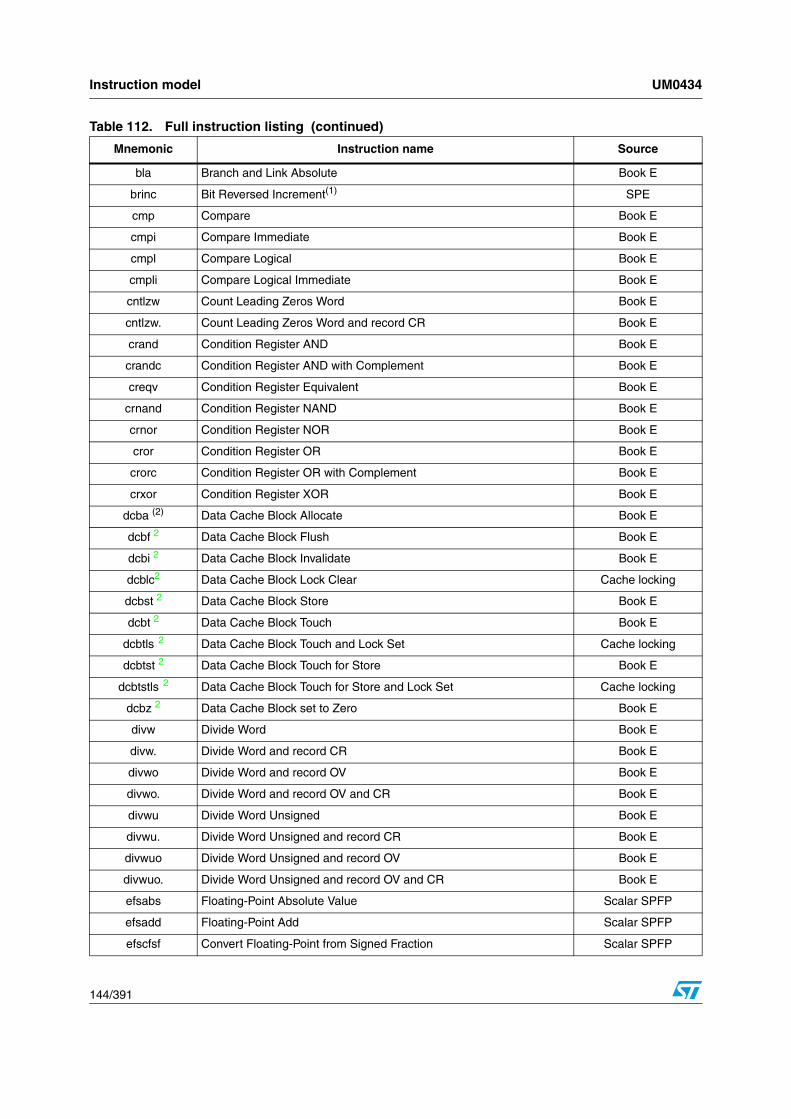
Instruction model UM0434
144/391
bla Branch and Link Absolute Book E
brinc Bit Reversed Increment(1) SPE
cmp Compare Book E
cmpi Compare Immediate Book E
cmpl Compare Logical Book E
cmpli Compare Logical Immediate Book E
cntlzw Count Leading Zeros Word Book E
cntlzw. Count Leading Zeros Word and record CR Book E
crand Condition Register AND Book E
crandc Condition Register AND with Complement Book E
creqv Condition Register Equivalent Book E
crnand Condition Register NAND Book E
crnor Condition Register NOR Book E
cror Condition Register OR Book E
crorc Condition Register OR with Complement Book E
crxor Condition Register XOR Book E
dcba (2) Data Cache Block Allocate Book E
dcbf 2 Data Cache Block Flush Book E
dcbi 2 Data Cache Block Invalidate Book E
dcblc2 Data Cache Block Lock Clear Cache locking
dcbst 2 Data Cache Block Store Book E
dcbt 2 Data Cache Block Touch Book E
dcbtls 2 Data Cache Block Touch and Lock Set Cache locking
dcbtst 2 Data Cache Block Touch for Store Book E
dcbtstls 2 Data Cache Block Touch for Store and Lock Set Cache locking
dcbz 2 Data Cache Block set to Zero Book E
divw Divide Word Book E
divw. Divide Word and record CR Book E
divwo Divide Word and record OV Book E
divwo. Divide Word and record OV and CR Book E
divwu Divide Word Unsigned Book E
divwu. Divide Word Unsigned and record CR Book E
divwuo Divide Word Unsigned and record OV Book E
divwuo. Divide Word Unsigned and record OV and CR Book E
efsabs Floating-Point Absolute Value Scalar SPFP
efsadd Floating-Point Add Scalar SPFP
efscfsf Convert Floating-Point from Signed Fraction Scalar SPFP
Table 112. Full instruction listing (continued)
Mnemonic Instruction name Source

UM0434 Instruction model
145/391
efscfsi Convert Floating-Point from Signed Integer Scalar SPFP
efscfuf Convert Floating-Point from Unsigned Fraction Scalar SPFP
efscfui Convert Floating-Point from Unsigned Integer Scalar SPFP
efscmpeq Floating-Point Compare Equal Scalar SPFP
efscmpgt Floating-Point Compare Greater Than Scalar SPFP
efscmplt Floating-Point Compare Less Than Scalar SPFP
efsctsf Convert Floating-Point to Signed Fraction Scalar SPFP
efsctsi Convert Floating-Point to Signed Integer Scalar SPFP
efsctsiz Convert floating-point to signed integer with round toward zero Scalar SPFP
efsctuf Convert Floating-Point to Unsigned Fraction Scalar SPFP
efsctui Convert Floating-Point to Unsigned Integer Scalar SPFP
efsctuiz Convert floating-point to unsigned integer with round toward zero Scalar SPFP
efsdiv Floating-Point Divide Scalar SPFP
efsmul Floating-Point Multiply Scalar SPFP
efsnabs Floating-Point Negative Absolute Value Scalar SPFP
efsneg Floating-Point Negate Scalar SPFP
efssub Floating-Point Subtract Scalar SPFP
efststeq Floating-Point Test Equal Scalar SPFP
efststgt Floating-Point Test Greater Than Scalar SPFP
efststlt Floating-Point Test Less Than Scalar SPFP
eqv Equivalent Book E
eqv. Equivalent and record CR Book E
evabs Vector Absolute Value SPE
evaddiw Vector Add Immediate Word SPE
evaddsmiaaw Vector Add Signed, Modulo, Integer to Accumulator Word SPE
evaddssiaaw Vector Add Signed, Saturate, Integer to Accumulator Word SPE
evaddumiaaw Vector Add Unsigned, Modulo, Integer to Accumulator Word SPE
evaddusiaaw Vector Add Unsigned, Saturate, Integer to Accumulator Word SPE
evaddw Vector Add Word SPE
evand Vector AND SPE
evandc Vector AND with Complement SPE
evcmpeq Vector Compare Equal SPE
evcmpgts Vector Compare Greater Than Signed SPE
evcmpgtu Vector Compare Greater Than Unsigned SPE
evcmplts Vector Compare Less Than Signed SPE
evcmpltu Vector Compare Less Than Unsigned SPE
evcntlsw Vector Count Leading Sign Bits Word SPE
Table 112. Full instruction listing (continued)
Mnemonic Instruction name Source
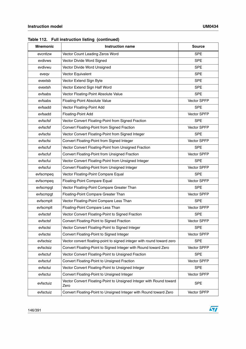
Instruction model UM0434
146/391
evcntlzw Vector Count Leading Zeros Word SPE
evdivws Vector Divide Word Signed SPE
evdivwu Vector Divide Word Unsigned SPE
eveqv Vector Equivalent SPE
evextsb Vector Extend Sign Byte SPE
evextsh Vector Extend Sign Half Word SPE
evfsabs Vector Floating-Point Absolute Value SPE
evfsabs Floating-Point Absolute Value Vector SPFP
evfsadd Vector Floating-Point Add SPE
evfsadd Floating-Point Add Vector SPFP
evfscfsf Vector Convert Floating-Point from Signed Fraction SPE
evfscfsf Convert Floating-Point from Signed Fraction Vector SPFP
evfscfsi Vector Convert Floating-Point from Signed Integer SPE
evfscfsi Convert Floating-Point from Signed Integer Vector SPFP
evfscfuf Vector Convert Floating-Point from Unsigned Fraction SPE
evfscfuf Convert Floating-Point from Unsigned Fraction Vector SPFP
evfscfui Vector Convert Floating-Point from Unsigned Integer SPE
evfscfui Convert Floating-Point from Unsigned Integer Vector SPFP
evfscmpeq Vector Floating-Point Compare Equal SPE
evfscmpeq Floating-Point Compare Equal Vector SPFP
evfscmpgt Vector Floating-Point Compare Greater Than SPE
evfscmpgt Floating-Point Compare Greater Than Vector SPFP
evfscmplt Vector Floating-Point Compare Less Than SPE
evfscmplt Floating-Point Compare Less Than Vector SPFP
evfsctsf Vector Convert Floating-Point to Signed Fraction SPE
evfsctsf Convert Floating-Point to Signed Fraction Vector SPFP
evfsctsi Vector Convert Floating-Point to Signed Integer SPE
evfsctsi Convert Floating-Point to Signed Integer Vector SPFP
evfsctsiz Vector convert floating-point to signed integer with round toward zero SPE
evfsctsiz Convert Floating-Point to Signed Integer with Round toward Zero Vector SPFP
evfsctuf Vector Convert Floating-Point to Unsigned Fraction SPE
evfsctuf Convert Floating-Point to Unsigned Fraction Vector SPFP
evfsctui Vector Convert Floating-Point to Unsigned Integer SPE
evfsctui Convert Floating-Point to Unsigned Integer Vector SPFP
evfsctuizVector Convert Floating-Point to Unsigned Integer with Round toward Zero
SPE
evfsctuiz Convert Floating-Point to Unsigned Integer with Round toward Zero Vector SPFP
Table 112. Full instruction listing (continued)
Mnemonic Instruction name Source

UM0434 Instruction model
147/391
evfsdiv Vector Floating-Point Divide SPE
evfsdiv Floating-Point Divide Vector SPFP
evfsmul Vector Floating-Point Multiply SPE
evfsmul Floating-Point Multiply Vector SPFP
evfsnabs Vector Floating-Point Negative Absolute Value SPE
evfsnabs Floating-Point Negative Absolute Value Vector SPFP
evfsneg Vector Floating-Point Negate SPE
evfsneg Floating-Point Negate Vector SPFP
evfssub Vector Floating-Point Subtract SPE
evfssub Floating-Point Subtract Vector SPFP
evfststeq Vector Floating-Point Test Equal SPE
evfststeq Floating-Point Test Equal Vector SPFP
evfststgt Vector Floating-Point Test Greater Than SPE
evfststgt Floating-Point Test Greater Than Vector SPFP
evfststlt Vector Floating-Point Test Less Than SPE
evfststlt Floating-Point Test Less Than Vector SPFP
evldd Vector Load Double Word into Double Word SPE
evlddx Vector Load Double Word into Double Word Indexed SPE
evldh Vector Load Double into Half Words SPE
evldhx Vector Load Double into Half Words Indexed SPE
evldw Vector Load Double into Two Words SPE
evldwx Vector Load Double into Two Words Indexed SPE
evlhhesplat Vector Load Half Word into Half Words Even and Splat SPE
evlhhesplatx Vector Load Half Word into Half Words Even and Splat Indexed SPE
evlhhossplat Vector Load Half Word into Half Word Odd Signed and Splat SPE
evlhhossplatx Vector Load Half Word into Half Word Odd Signed and Splat Indexed SPE
evlhhousplat Vector Load Half Word into Half Word Odd Unsigned and Splat SPE
evlhhousplatxVector Load Half Word into Half Word Odd Unsigned and Splat Indexed
SPE
evlwhe Vector Load Word into Two Half Words Even SPE
evlwhex Vector Load Word into Two Half Words Even Indexed SPE
evlwhos Vector Load Word into Half Words Odd Signed (with sign extension) SPE
evlwhosxVector Load Word into Half Words Odd Signed Indexed (with sign extension)
SPE
evlwhou Vector Load Word into Two Half Words Odd Unsigned (zero-extended) SPE
evlwhouxVector load word into two half words odd unsigned indexed (zero-extended)
SPE
evlwhsplat Vector Load Word into Half Words and Splat SPE
Table 112. Full instruction listing (continued)
Mnemonic Instruction name Source

Instruction model UM0434
148/391
evlwhsplatx Vector Load Word into Half Words and Splat Indexed SPE
evlwwsplat Vector Load Word into Word and Splat SPE
evlwwsplatx Vector Load Word into Word and Splat Indexed SPE
evmergehi Vector Merge High SPE
evmergehilo Vector Merge High/Low SPE
evmergelo Vector Merge Low SPE
evmergelohi Vector Merge Low/High SPE
evmhegsmfaaMultiply Half Words, Even, Guarded, Signed, Modulo, Fractional and Accumulate
SPE
evmhegsmfanMultiply Half Words, Even, Guarded, Signed, Modulo, Fractional and Accumulate Negative
SPE
evmhegsmiaaMultiply half words, even, guarded, signed, modulo, integer and accumulate
SPE
evmhegsmianMultiply Half Words, Even, Guarded, Signed, Modulo, Integer and Accumulate Negative
SPE
evmhegumiaaMultiply Half Words, Even, Guarded, Unsigned, Modulo, Integer and Accumulate
SPE
evmhegumianMultiply Half Words, Even, Guarded, Unsigned, Modulo, Integer and Accumulate Negative
SPE
evmhesmf Vector Multiply Half Words, Even, Signed, Modulo, Fractional SPE
evmhesmfaVector Multiply Half Words, Even, Signed, Modulo, Fractional, Accumulate
SPE
evmhesmfaawVector Multiply Half Words, Even, Signed, Modulo, Fractional and Accumulate into Words
SPE
evmhesmfanwVector Multiply Half Words, Even, Signed, Modulo, Fractional and Accumulate Negative into Words
SPE
evmhesmi Vector Multiply Half Words, Even, Signed, Modulo, Integer SPE
evmhesmiaVector Multiply Half Words, Even, Signed, Modulo, Integer, Accumulate
SPE
evmhesmiaawVector Multiply Half Words, Even, Signed, Modulo, Integer and Accumulate into Words
SPE
evmhesmianwVector Multiply Half Words, Even, Signed, Modulo, Integer and Accumulate Negative into Words
SPE
evmhessf Vector Multiply Half Words, Even, Signed, Saturate, Fractional SPE
evmhessfaVector Multiply Half Words, Even, Signed, Saturate, Fractional, Accumulate
SPE
evmhessfaawVector Multiply Half Words, Even, Signed, Saturate, Fractional and Accumulate into Words
SPE
evmhessfanwVector Multiply Half Words, Even, Signed, Saturate, Fractional and Accumulate Negative into Words
SPE
evmhessiaawVector Multiply Half Words, Even, Signed, Saturate, Integer and Accumulate into Words
SPE
Table 112. Full instruction listing (continued)
Mnemonic Instruction name Source

UM0434 Instruction model
149/391
evmhessianwVector Multiply Half Words, Even, Signed, Saturate, Integer and Accumulate Negative into Words
SPE
evmheumi Vector Multiply Half Words, Even, Unsigned, Modulo, Integer SPE
evmheumiaVector Multiply Half Words, Even, Unsigned, Modulo, Integer, Accumulate
SPE
evmheumiaawVector Multiply Half Words, Even, Unsigned, Modulo, Integer and Accumulate into Words
SPE
evmheumianwVector Multiply Half Words, Even, Unsigned, Modulo, Integer and Accumulate Negative into Words
SPE
evmheusiaawVector Multiply Half Words, Even, Unsigned, Saturate, Integer and Accumulate into Words
SPE
evmheusianwVector Multiply Half Words, Even, Unsigned, Saturate, Integer and Accumulate Negative into Words
SPE
evmhogsmfaaMultiply Half Words, Odd, Guarded, Signed, Modulo, Fractional and Accumulate
SPE
evmhogsmfanMultiply Half Words, Odd, Guarded, Signed, Modulo, Fractional and Accumulate Negative
SPE
evmhogsmiaaMultiply Half Words, Odd, Guarded, Signed, Modulo, Integer and Accumulate
SPE
evmhogsmianMultiply Half Words, Odd, Guarded, Signed, Modulo, Integer and Accumulate Negative
SPE
evmhogumiaaMultiply Half Words, Odd, Guarded, Unsigned, Modulo, Integer and Accumulate
SPE
evmhogumianMultiply Half Words, Odd, Guarded, Unsigned, Modulo, Integer and Accumulate Negative
SPE
evmhosmf Vector Multiply Half Words, Odd, Signed, Modulo, Fractional SPE
evmhosmfaVector Multiply Half Words, Odd, Signed, Modulo, Fractional, Accumulate
SPE
evmhosmfaawVector Multiply Half Words, Odd, Signed, Modulo, Fractional and Accumulate into Words
SPE
evmhosmfanwVector Multiply Half Words, Odd, Signed, Modulo, Fractional and Accumulate Negative into Words
SPE
evmhosmi Vector Multiply Half Words, Odd, Signed, Modulo, Integer SPE
evmhosmia Vector Multiply Half Words, Odd, Signed, Modulo, Integer, Accumulate SPE
evmhosmiaawVector Multiply Half Words, Odd, Signed, Modulo, Integer and Accumulate into Words
SPE
evmhosmianwVector Multiply Half Words, Odd, Signed, Modulo, Integer and Accumulate Negative into Words
SPE
evmhossf Vector Multiply Half Words, Odd, Signed, Saturate, Fractional SPE
evmhossfaVector Multiply Half Words, Odd, Signed, Saturate, Fractional, Accumulate
SPE
evmhossfaawVector Multiply Half Words, Odd, Signed, Saturate, Fractional and Accumulate into Words
SPE
Table 112. Full instruction listing (continued)
Mnemonic Instruction name Source
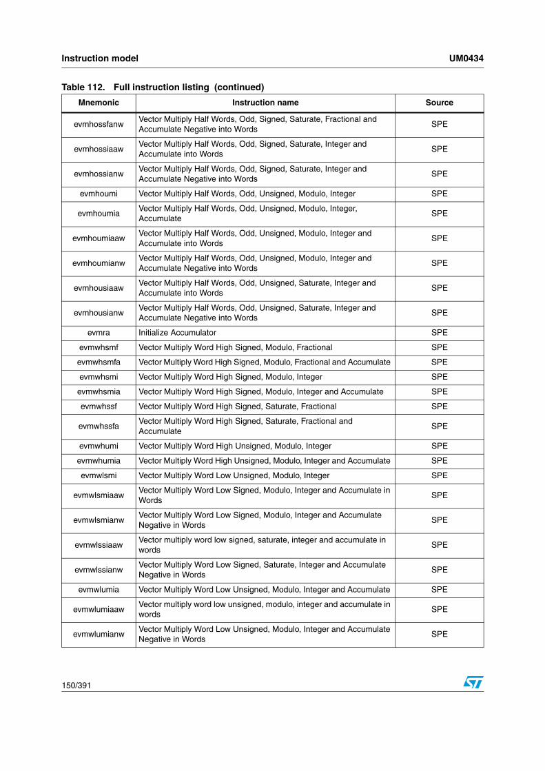
Instruction model UM0434
150/391
evmhossfanwVector Multiply Half Words, Odd, Signed, Saturate, Fractional and Accumulate Negative into Words
SPE
evmhossiaawVector Multiply Half Words, Odd, Signed, Saturate, Integer and Accumulate into Words
SPE
evmhossianwVector Multiply Half Words, Odd, Signed, Saturate, Integer and Accumulate Negative into Words
SPE
evmhoumi Vector Multiply Half Words, Odd, Unsigned, Modulo, Integer SPE
evmhoumiaVector Multiply Half Words, Odd, Unsigned, Modulo, Integer, Accumulate
SPE
evmhoumiaawVector Multiply Half Words, Odd, Unsigned, Modulo, Integer and Accumulate into Words
SPE
evmhoumianwVector Multiply Half Words, Odd, Unsigned, Modulo, Integer and Accumulate Negative into Words
SPE
evmhousiaawVector Multiply Half Words, Odd, Unsigned, Saturate, Integer and Accumulate into Words
SPE
evmhousianwVector Multiply Half Words, Odd, Unsigned, Saturate, Integer and Accumulate Negative into Words
SPE
evmra Initialize Accumulator SPE
evmwhsmf Vector Multiply Word High Signed, Modulo, Fractional SPE
evmwhsmfa Vector Multiply Word High Signed, Modulo, Fractional and Accumulate SPE
evmwhsmi Vector Multiply Word High Signed, Modulo, Integer SPE
evmwhsmia Vector Multiply Word High Signed, Modulo, Integer and Accumulate SPE
evmwhssf Vector Multiply Word High Signed, Saturate, Fractional SPE
evmwhssfaVector Multiply Word High Signed, Saturate, Fractional and Accumulate
SPE
evmwhumi Vector Multiply Word High Unsigned, Modulo, Integer SPE
evmwhumia Vector Multiply Word High Unsigned, Modulo, Integer and Accumulate SPE
evmwlsmi Vector Multiply Word Low Unsigned, Modulo, Integer SPE
evmwlsmiaawVector Multiply Word Low Signed, Modulo, Integer and Accumulate in Words
SPE
evmwlsmianwVector Multiply Word Low Signed, Modulo, Integer and Accumulate Negative in Words
SPE
evmwlssiaawVector multiply word low signed, saturate, integer and accumulate in words
SPE
evmwlssianwVector Multiply Word Low Signed, Saturate, Integer and Accumulate Negative in Words
SPE
evmwlumia Vector Multiply Word Low Unsigned, Modulo, Integer and Accumulate SPE
evmwlumiaawVector multiply word low unsigned, modulo, integer and accumulate in words
SPE
evmwlumianwVector Multiply Word Low Unsigned, Modulo, Integer and Accumulate Negative in Words
SPE
Table 112. Full instruction listing (continued)
Mnemonic Instruction name Source

UM0434 Instruction model
151/391
evmwlusiaawVector Multiply Word Low Unsigned, Saturate, Integer and Accumulate in Words
SPE
evmwlusianwVector Multiply Word Low Unsigned, Saturate, Integer and Accumulate Negative in Words
SPE
evmwsmf Vector Multiply Word Signed, Modulo, Fractional SPE
evmwsmfa Vector Multiply Word Signed, Modulo, Fractional and Accumulate SPE
evmwsmfaa Vector Multiply Word Signed, Modulo, Fractional and Accumulate SPE
evmwsmfanVector Multiply Word Signed, Modulo, Fractional and Accumulate Negative
SPE
evmwsmi Vector Multiply Word Signed, Modulo, Integer SPE
evmwsmia Vector Multiply Word Signed, Modulo, Integer and Accumulate SPE
evmwsmiaa Vector Multiply Word Signed, Modulo, Integer and Accumulate SPE
evmwsmianVector Multiply Word Signed, Modulo, Integer and Accumulate Negative
SPE
evmwssf Vector Multiply Word Signed, Saturate, Fractional SPE
evmwssfa Vector Multiply Word Signed, Saturate, Fractional and Accumulate SPE
evmwssfaa Vector Multiply Word Signed, Saturate, Fractional and Accumulate SPE
evmwssfanVector Multiply Word Signed, Saturate, Fractional and Accumulate Negative
SPE
evmwumi Vector Multiply Word Unsigned, Modulo, Integer SPE
evmwumia Vector Multiply Word Unsigned, Modulo, Integer and Accumulate SPE
evmwumiaa Vector Multiply Word Unsigned, Modulo, Integer and Accumulate SPE
evmwumianVector Multiply Word Unsigned, Modulo, Integer and Accumulate Negative
SPE
evnand Vector NAND SPE
evneg Vector Negate SPE
evnor Vector NOR SPE
evor Vector OR SPE
evorc Vector OR with Complement SPE
evrlw Vector Rotate Left Word SPE
evrlwi Vector Rotate Left Word Immediate SPE
evrndw Vector Round Word SPE
evsel Vector Select SPE
evslw Vector Shift Left Word SPE
evslwi Vector Shift Left Word Immediate SPE
evsplatfi Vector Splat Fractional Immediate SPE
evsplati Vector Splat Immediate SPE
evsrwis Vector Shift Right Word Immediate Signed SPE
evsrwiu Vector Shift Right Word Immediate Unsigned SPE
Table 112. Full instruction listing (continued)
Mnemonic Instruction name Source

Instruction model UM0434
152/391
evsrws Vector Shift Right Word Signed SPE
evsrwu Vector Shift Right Word Unsigned SPE
evstdd Vector Store Double of Double SPE
evstddx Vector Store Double of Double Indexed SPE
evstdh Vector Store Double of Four Half Words SPE
evstdhx Vector Store Double of Four Half Words Indexed SPE
evstdw Vector Store Double of Two Words SPE
evstdwx Vector Store Double of Two Words Indexed SPE
evstwhe Vector Store Word of Two Half Words from Even SPE
evstwhex Vector Store Word of Two Half Words from Even Indexed SPE
evstwho Vector Store Word of Two Half Words from Odd SPE
evstwhox Vector Store Word of Two Half Words from Odd Indexed SPE
evstwwe Vector Store Word of Word from Even SPE
evstwwex Vector Store Word of Word from Even Indexed SPE
evstwwo Vector Store Word of Word from Odd SPE
evstwwox Vector Store Word of Word from Odd Indexed SPE
evsubfsmiaaw Vector Subtract Signed, Modulo, Integer to Accumulator Word SPE
evsubfssiaaw Vector Subtract Signed, Saturate, Integer to Accumulator Word SPE
evsubfumiaaw Vector Subtract Unsigned, Modulo, Integer to Accumulator Word SPE
evsubfusiaaw Vector Subtract Unsigned, Saturate, Integer to Accumulator Word SPE
evsubfw Vector Subtract from Word SPE
evsubifw Vector Subtract Immediate from Word SPE
evxor Vector XOR SPE
extsb Extend Sign Byte Book E
extsb. Extend Sign Byte and record CR Book E
extsh Extend Sign Half Word Book E
extsh. Extend Sign Half Word and record CR Book E
e_add16i Add Immediate VLE (16-bit opcodes)
e_add2i. Add (2 operand) Immediate and Record CR VLE (16-bit opcodes)
e_add2is Add (2 operand) Immediate Shifted VLE (16-bit opcodes)
e_addi Add Immediate VLE (16-bit opcodes)
e_addi. Add Immediate and Record VLE (16-bit opcodes)
e_addic Add Immediate Carrying VLE (16-bit opcodes)
e_addic. Add Immediate Carrying and Record VLE (16-bit opcodes)
e_and2i. AND (2 operand) Immediate & record CR VLE (16-bit opcodes)
e_and2is. AND (2 operand) Immediate Shifted & record CR VLE (16-bit opcodes)
e_andi AND Immediate VLE (16-bit opcodes)
Table 112. Full instruction listing (continued)
Mnemonic Instruction name Source

UM0434 Instruction model
153/391
e_andi. AND Immediate and Record VLE (16-bit opcodes)
e_b Branch VLE (16-bit opcodes)
e_bc Branch Conditional VLE (16-bit opcodes)
e_bcl Branch Conditional & Link VLE (16-bit opcodes)
e_bl Branch & Link VLE (16-bit opcodes)
e_cmp16i Compare Immediate VLE (16-bit opcodes)
e_cmph Compare Halfword VLE (16-bit opcodes)
e_cmph16i Compare Halfword Immediate VLE (16-bit opcodes)
e_cmphl Compare Halfword Logical VLE (16-bit opcodes)
e_cmphl16i Compare Halfword Logical Immediate VLE (16-bit opcodes)
e_cmpi Compare Immediate VLE (16-bit opcodes)
e_cmpl16i Compare Logical Immediate VLE (16-bit opcodes)
e_cmpli Compare Logical Immediate VLE (16-bit opcodes)
e_crand Condition Register AND VLE (16-bit opcodes)
e_crandc Condition Register AND with Complement VLE (16-bit opcodes)
e_creqv Condition Register Equivalent VLE (16-bit opcodes)
e_crnand Condition Register NAND VLE (16-bit opcodes)
e_crnor Condition Register NOR VLE (16-bit opcodes)
e_cror Condition Register OR VLE (16-bit opcodes)
e_crorc Condition Register OR with Complement VLE (16-bit opcodes)
e_crxor Condition Register XOR VLE (16-bit opcodes)
e_lbz Load Byte & Zero VLE (16-bit opcodes)
e_lbzu Load Byte & Zero with Update VLE (16-bit opcodes)
e_lha Load Halfword Algebraic VLE (16-bit opcodes)
e_lhau Load Halfword Algebraic With Update VLE (16-bit opcodes)
e_lhz Load Halfword & Zero VLE (16-bit opcodes)
e_lhzu Load Halfword & Zero with Update VLE (16-bit opcodes)
e_li Load Immediate VLE (16-bit opcodes)
e_lis Load Immediate Shifted VLE (16-bit opcodes)
e_lmw Load Multiple Word VLE (16-bit opcodes)
e_lwz Load Word & Zero VLE (16-bit opcodes)
e_lwzu Load Word & Zero with Update VLE (16-bit opcodes)
e_mcrf Move Condition Register Field VLE (16-bit opcodes)
e_mull2i Multiply Low Word (2 operand) Immediate VLE (16-bit opcodes)
e_mulli Multiply Low Immediate VLE (16-bit opcodes)
e_or2i OR (2 operand) Immediate VLE (16-bit opcodes)
e_or2is OR (2 operand) Immediate Shifted VLE (16-bit opcodes)
Table 112. Full instruction listing (continued)
Mnemonic Instruction name Source

Instruction model UM0434
154/391
e_ori OR Immediate VLE (16-bit opcodes)
e_ori. OR Immediate and Record VLE (16-bit opcodes)
e_rlw Rotate Left Word VLE (16-bit opcodes)
e_rlw. Rotate Left Word & record CR VLE (16-bit opcodes)
e_rlwi Rotate Left Word Immediate VLE (16-bit opcodes)
e_rlwi. Rotate Left Word Immediate & record CR VLE (16-bit opcodes)
e_rlwimi Rotate Left Word Immed then Mask Insert VLE (16-bit opcodes)
e_rlwinm Rotate Left Word Immed then AND with Mask VLE (16-bit opcodes)
e_slwi Shift Left Word Immediate VLE (16-bit opcodes)
e_slwi. Shift Left Word Immediate & record CR VLE (16-bit opcodes)
e_srwi Shift Right Word Immediate VLE (16-bit opcodes)
e_srwi. Shift Right Word Immediate & record CR VLE (16-bit opcodes)
e_stb Store Byte VLE (16-bit opcodes)
e_stbu Store Byte with Update VLE (16-bit opcodes)
e_sth Store Halfword VLE (16-bit opcodes)
e_sthu Store Halfword with Update VLE (16-bit opcodes)
e_stmw Store Multiple Word VLE (16-bit opcodes)
e_stw Store Word VLE (16-bit opcodes)
e_stwu Store Word with Update VLE (16-bit opcodes)
e_subfic Subtract from Immediate Carrying VLE (16-bit opcodes)
e_subfic. Subtract from Immediate and Record VLE (16-bit opcodes)
e_xori XOR Immediate VLE (16-bit opcodes)
e_xori. XOR Immediate and Record VLE (16-bit opcodes)
icbi 2 Instruction Cache Block Invalidate Book E
icblc 2 Instruction Cache Block Lock Clear Cache locking
icbt 2 Instruction Cache Block Touch Book E
icbtls 2 Instruction Cache Block Touch and Lock Set Cache locking
isel Integer Select EIS
isync Instruction Synchronize Book E
lbz Load Byte and Zero Book E
lbzu Load Byte and Zero with Update Book E
lbzux Load Byte and Zero with Update Indexed Book E
lbzx Load Byte and Zero Indexed Book E
lha Load Half Word Algebraic Book E
lhau Load Half Word Algebraic with Update Book E
lhaux Load Half Word Algebraic with Update Indexed Book E
lhax Load Half Word Algebraic Indexed Book E
Table 112. Full instruction listing (continued)
Mnemonic Instruction name Source

UM0434 Instruction model
155/391
lhbrx Load Half Word Byte-Reverse Indexed Book E
lhz Load Half Word and Zero Book E
lhzu Load Half Word and Zero with Update Book E
lhzux Load Half Word and Zero with Update Indexed Book E
lhzx Load Half Word and Zero Indexed Book E
lmw Load Multiple Word Book E
lwarx Load Word and Reserve Indexed Book E
lwbrx Load Word Byte-Reverse Indexed Book E
lwz Load Word and Zero Book E
lwzu Load Word and Zero with Update Book E
lwzux Load Word and Zero with Update Indexed Book E
lwzx Load Word and Zero Indexed Book E
mbar(3) Memory Barrier Book E
mcrf Move Condition Register Field Book E
mcrxr Move to Condition Register from XER Book E
mfcr Move From Condition Register Book E
mfdcr(4) Move From Device Control Register Book E
mfdcrx4 Move From Device Control Register Indexed Book E
mfmsr Move From Machine State Register Book E
mfspr Move From Special Purpose Register Book E
msync3 Memory Synchronize Book E
mtcrf Move To Condition Register Fields Book E
mtdcr4 Move To Device Control Register Book E
mtdcrx4 Move To Device Control Register Indexed Book E
mtmsr Move To Machine State Register Book E
mtspr Move To Special Purpose Register Book E
mulhw Multiply High Word Book E
mulhw. Multiply High Word and record CR Book E
mulhwu Multiply High Word Unsigned Book E
mulhwu. Multiply High Word Unsigned and record CR Book E
mulli Multiply Low Immediate Book E
mullw Multiply Low Word Book E
mullw. Multiply Low Word and record CR Book E
mullwo Multiply Low Word and record OV Book E
mullwo. Multiply Low Word and record OV and CR Book E
nand NAND Book E
nand. NAND and record CR Book E
Table 112. Full instruction listing (continued)
Mnemonic Instruction name Source

Instruction model UM0434
156/391
neg Negate Book E
neg. Negate and record CR Book E
nego Negate and record OV Book E
nego. Negate and record OV and record CR Book E
nor NOR Book E
nor. NOR and record CR Book E
or OR Book E
or. OR and record CR Book E
orc OR with Complement Book E
orc. OR with Complement and record CR Book E
ori OR Immediate Book E
oris OR Immediate Shifted Book E
rfci Return From Critical Interrupt Book E
rfdi Return From Debug Interrupt Debug
rfi Return From Interrupt Book E
rlwimi Rotate Left Word Immed then Mask Insert Book E
rlwimi. Rotate Left Word Immed then Mask Insert and record CR Book E
rlwinm Rotate Left Word Immed then AND with Mask Book E
rlwinm. Rotate Left Word Immed then AND with Mask and record CR Book E
rlwnm Rotate Left Word then AND with Mask Book E
rlwnm. Rotate Left Word then AND with Mask and record CR Book E
sc System Call Book E
se_add Add VLE (32-bit opcodes)
se_addi Add Immediate VLE (32-bit opcodes)
se_and AND VLE (32-bit opcodes)
se_and. AND and Record VLE (32-bit opcodes)
se_andc AND with Complement VLE (32-bit opcodes)
se_andi And Immediate VLE (32-bit opcodes)
se_b Branch VLE (32-bit opcodes)
se_bc Branch Conditional VLE (32-bit opcodes)
se_bclri Bit Clear Immediate VLE (32-bit opcodes)
se_bctr Branch to Count Register VLE (32-bit opcodes)
se_bctrl Branch to Count Register & Link VLE (32-bit opcodes)
se_bgeni Bit Generate Immediate VLE (32-bit opcodes)
se_bl Branch and Link VLE (32-bit opcodes)
se_blr Branch to Link Register VLE (32-bit opcodes)
se_blrl Branch to Link Register & Link VLE (32-bit opcodes)
Table 112. Full instruction listing (continued)
Mnemonic Instruction name Source

UM0434 Instruction model
157/391
se_bmaski Bit Mask Generate Immediate VLE (32-bit opcodes)
se_bseti Bit Set Immediate VLE (32-bit opcodes)
se_btsti Bit Test Immediate VLE (32-bit opcodes)
se_cmp Compare VLE (32-bit opcodes)
se_cmph Compare Halfword VLE (32-bit opcodes)
se_cmphl Compare Halfword Logical VLE (32-bit opcodes)
se_cmpi Compare Immediate VLE (32-bit opcodes)
se_cmpl Compare Logical VLE (32-bit opcodes)
se_cmpli Compare Logical Immediate VLE (32-bit opcodes)
se_extsb Extend Sign Byte VLE (32-bit opcodes)
se_extsh Extend Sign Halfword VLE (32-bit opcodes)
se_extzb Extend with Zeros Byte VLE (32-bit opcodes)
se_extzh Extend with Zeros Halfword VLE (32-bit opcodes)
se_illegal Illegal VLE (32-bit opcodes)
se_isync Instruction Synchronize VLE (32-bit opcodes)
se_lbz Load Byte and Zero VLE (32-bit opcodes)
se_lhz Load Halfword and Zero VLE (32-bit opcodes)
se_li Load Immediate VLE (32-bit opcodes)
se_lwz Load Word and Zero VLE (32-bit opcodes)
se_mfar Move from Alternate Register VLE (32-bit opcodes)
se_mfctr Move From Count Register VLE (32-bit opcodes)
se_mflr Move From Link Register VLE (32-bit opcodes)
se_mr Move Register VLE (32-bit opcodes)
se_mtar Move to Alternate Register VLE (32-bit opcodes)
se_mtctr Move To Count Register VLE (32-bit opcodes)
se_mtlr Move To Link Register VLE (32-bit opcodes)
se_mullw Multiply Low Word VLE (32-bit opcodes)
se_neg Negate VLE (32-bit opcodes)
se_not NOT VLE (32-bit opcodes)
se_or OR VLE (32-bit opcodes)
se_rfci Return From Critical Interrupt VLE (32-bit opcodes)
se_rfdi Return From Debug Interrupt VLE (32-bit opcodes)
se_rfi Return From Interrupt VLE (32-bit opcodes)
se_sc System Call VLE (32-bit opcodes)
se_slw Shift Left Word VLE (32-bit opcodes)
se_slwi Shift Left Word Immediate VLE (32-bit opcodes)
se_sraw Shift Right Algebraic Word VLE (32-bit opcodes)
Table 112. Full instruction listing (continued)
Mnemonic Instruction name Source

Instruction model UM0434
158/391
se_srawi Shift Right Algebraic Word Immediate VLE (32-bit opcodes)
se_srw Shift Right Word VLE (32-bit opcodes)
se_srwi Shift Right Word Immediate VLE (32-bit opcodes)
se_stb Store Byte VLE (32-bit opcodes)
se_sth Store Halfword VLE (32-bit opcodes)
se_stw Store Word VLE (32-bit opcodes)
se_sub Subtract VLE (32-bit opcodes)
se_subf Subtract From VLE (32-bit opcodes)
se_subi Subtract Immediate VLE (32-bit opcodes)
se_subi. Subtract Immediate and Record VLE (32-bit opcodes)
slw Shift Left Word Book E
slw. Shift Left Word and record CR Book E
sraw Shift Right Algebraic Word Book E
sraw. Shift Right Algebraic Word and record CR Book E
srawi Shift Right Algebraic Word Immediate Book E
srawi. Shift Right Algebraic Word Immediate and record CR Book E
srw Shift Right Word Book E
srw. Shift Right Word and record CR Book E
stb Store Byte Book E
stbu Store Byte with Update Book E
stbux Store Byte with Update Indexed Book E
stbx Store Byte Indexed Book E
sth Store Half Word Book E
sthbrx Store Half Word Byte-Reverse Indexed Book E
sthu Store Half Word with Update Book E
sthux Store Half Word with Update Indexed Book E
sthx Store Half Word Indexed Book E
stmw Store Multiple Word Book E
stw Store Word Book E
stwbrx Store Word Byte-Reverse Indexed Book E
stwcx. Store Word Conditional Indexed and record CR Book E
stwu Store Word with Update Book E
stwux Store Word with Update Indexed Book E
stwx Store Word Indexed Book E
subf Subtract From Book E
subf. Subtract From and record CR Book E
subfc Subtract From Carrying Book E
Table 112. Full instruction listing (continued)
Mnemonic Instruction name Source

UM0434 Instruction model
159/391
subfc. Subtract From Carrying and record CR Book E
subfco Subtract From Carrying and record OV Book E
subfco. Subtract From Carrying and record OV and CR Book E
subfe Subtract From Extended with CA Book E
subfe. Subtract From Extended with CA and record CR Book E
subfeo Subtract From Extended with CA and record OV Book E
subfeo. Subtract From Extended with CA and record OV and CR Book E
subfic Subtract From Immediate Carrying Book E
subfme Subtract From Minus One Extended with CA Book E
subfme. Subtract From Minus One Extended with CA and record CR Book E
subfmeo Subtract From Minus One Extended with CA and record OV Book E
subfmeo. Subtract From Minus One Extended with CA and record OV & CR Book E
subfo Subtract From and record OV Book E
subfo. Subtract From and record OV and CR Book E
subfze Subtract From Zero Extended with CA Book E
subfze. Subtract From Zero Extended with CA and record CR Book E
subfzeo Subtract From Zero Extended with CA and record OV Book E
subfzeo. Subtract From Zero Extended with CA and record OV and CR Book E
tlbivax TLB Invalidate Virtual Address Indexed Book E
tlbre TLB Read Entry Book E
tlbsx TLB Search Indexed Book E
tlbsync TLB Synchronize Book E
tlbwe TLB Write Entry Book E
tw Trap Word Book E
twi Trap Word Immediate Book E
wrtee Write External Enable Book E
wrteei Write External Enable Immediate Book E
xor XOR Book E
xor. XOR and record CR Book E
xori XOR Immediate Book E
xoris XOR Immediate Shifted Book E
1. An implementation can restrict the No. of bits shown in a mask. Devices using 16-bit instructions are limited to 16 bits, which allows the user to perform bit-reversed address computations for 65536 byte samples.
2. Not supported by e200z3 unless the integrated device includes a cache; treated as no-ops, with the exception of dcbz, which results in an alignment interrupt, and dcbi, which is treated as a privileged no-op.
3. See Chapter 5.7: Memory synchronization and reservation instructions
4. The core CPU will take an illegal instruction exception for unsupported DCR values.
Table 112. Full instruction listing (continued)
Mnemonic Instruction name Source

Interrupts and exceptions UM0434
160/391
6 Interrupts and exceptions
This chapter provides a general description of the PowerPC Book E interrupt and exception model and gives details of the additions and changes to that model that are implemented in the e200z3 core. This chapter identifies features defined by Book E, the Freescale Book E implementation standards (EIS), and the e200z3 implementation.
6.1 OverviewBook E defines the mechanisms by which the e200z3 core implements interrupts and exceptions. Note the following definitions:
Interrupt Action in which the processor saves its old context and begins execution at a predetermined interrupt handler address
Exceptions Events that, if enabled, cause the processor to take an interrupt
The PowerPC exception mechanism allows the processor to change to supervisor state for the following reasons:
● As a result of unusual conditions (exceptions) arising in the execution of instructions
● As a response to the assertion of external signals, bus errors, or various internal conditions
When an interrupt occurs, information about the processor state held in the MSR and the address at which execution should resume after the interrupt is handled are saved to a pair of save/restore registers (SRR0/SRR1 for non-critical interrupts, CSRR0/CSRR1 for critical interrupts, or DSRR0/DSRR1 for debug interrupts when the debug APU is enabled), and the processor begins executing at an address (interrupt vector) determined by the interrupt vector prefix register (IVPR) and an interrupt-specific interrupt vector offset register (IVORn). Processing of instructions within the interrupt handler begins in supervisor mode.
Multiple exception conditions can map to a single interrupt vector and may be distinguished by examining registers associated with the interrupt. The exception syndrome register (ESR) is updated with information specific to the exception type when an interrupt occurs.
To prevent loss of state information, interrupt handlers must save the information stored in the save/restore registers soon after the interrupt is taken. Hardware supports nesting of critical interrupts within non-critical interrupts, and debug interrupts within both critical and non-critical interrupts. The interrupt handler must save necessary state information if interrupts of a given class are re-enabled within the handler.
The following terms are used to describe the stages of exception processing:
Recognition Exception recognition occurs when the condition that can cause an exception is identified by the processor.
Recognition is also referred to as an ‘exception event.’
Taken An interrupt is said to be taken when control of instruction execution is passed to the interrupt handler; that is, the context is saved, the instruction at the appropriate vector offset is fetched,
and the interrupt handler routine begins.
Handling Interrupt handling is performed by the software linked to the appropriatevector offset. Interrupt handling is begun in supervisor mode.

UM0434 Interrupts and exceptions
161/391
Returning from an interrupt is performed by executing the appropriate return from interrupt instruction (rfi, rfci, or rfdi), which restores state information from their respective save/restore registers and returns instruction fetching to the interrupted flow.
6.2 e200z3 interruptsThe Book E architecture specifies that interrupts can be precise or imprecise, synchronous or asynchronous, and critical or non-critical. These characteristics are described as follows:
● Asynchronous exceptions are caused by events external to the processor’s instruction execution.
● Synchronous exceptions are directly caused by instructions or by an event somehow synchronous to the program flow, such as a context switch.
● A precise interrupt architecturally guarantees that no instruction beyond the instruction causing the exception has (visibly) executed. An imprecise interrupt does not have this guarantee.
● Book E defines critical and non-critical interrupt types, and the e200z3 defines an implementation-specific debug APU that includes the debug interrupt type. Each interrupt type provides separate resources (save/restore registers and return from interrupt instructions) that allow interrupts of one type to not interfere with the state handling of an interrupt of another type.
Table 113 describes how these apply to the interrupts implemented by the e200z3 core.
The classifications in Table 113 are discussed in greater detail in Chapter 6.6: Interrupt definitions on page 168.” Interrupts implemented in the e200z3 and the exception conditions that cause them, are listed in Table 114. Note that although this table lists system reset, Book E does not define system reset as an interrupt and assigns no interrupt vector to it.
Table 113. Interrupt classifications
Interrupt typesSynchronous / asynchronous
Precise / imprecise
Critical / non-critical / debug
System reset Asynchronous, non-maskable
Imprecise —
Machine check — — Critical
Critical input
Watchdog timer Asynchronous,
maskableImprecise Critical
External input
Fixed-interval timer
Decrementer
Asynchronous, maskable
Imprecise Non-critical
Instruction based debug Synchronous Precise Critical/debug
Debug (UDE)
Debug imprecise Asynchronous Imprecise Critical/debug
Data storage
/ alignment / TLB
Instruction storage / TLB
Synchronous Precise Non-critical

Interrupts and exceptions UM0434
162/391
Table 114. Exceptions and conditions
Interrupt typeIVOR
n Cause Section/page
System reset (not an interrupt)
None(1)
Reset by assertion of p_reset_bWatchdog timer reset controlDebug reset control
—
Critical input 0(2) p_critint_b is asserted and MSR[CE]=1 Chapter 6.6.1
Machine check 1
p_mcp_b is asserted and MSR[ME] =1
ISI, ITLB error on first instruction fetch for an exception handler and current MSR[ME] = 1
Write bus error on buffered store or cache line push and current MSR[ME]=1
Bus error (XTE) with MSR[EE]=0 and current MSR[ME]=1
Chapter 6.6.2
Data storage 2
Access control
Byte ordering due to misaligned access across page boundary to pages with mismatched E bits
Precise external termination error (p_d_tea_b assertion and precise recognition) and MSR[EE]=1
Chapter 6.6.3
Instruction storage
3
Access controlPrecise external termination error (p_i_tea_b assertion and precise recognition) and MSR[EE]=1Byte ordering due to misaligned instruction across page boundary to pages with mismatched VLE bits, or access to page with VLE set, and E indicating little-endian.
Misaligned Instruction fetch due to a change of flow to an odd halfword instruction boundary on a Book E (non-VLE) instruction page, due to value in LR, CTR, or xSRR0
Chapter 6.6.4
External input 42. p_extint_b is asserted and MSR[EE]=1 Chapter 6.6.5
Alignment 5
lmw, stmw not word aligned
lwarx or stwcx. not word aligneddcbz with disabled cache, or no cache present, or to W or I storage
Chapter 6.6.6
Program 6Illegal, privileged, trap, floating-point enabled, APU enabled, unimplemented operation
Chapter 6.6.7
Floating-point unavailable
7 MSR[FP] = 0 and attempt to execute a Book E floating-point operation Chapter 6.6.8
System call 8 Execution of the system call (sc) instruction Chapter 6.6.9
APU unavailable 9 Unused by the e200z3 Chapter 6.6.10
Decrementer 10 As specified in Book E Chapter 6.6.11
Fixed-interval timer
11 As specified in Book E Chapter 6.6.12
Watchdog timer 12 As specified in Book E Chapter 6.6.13
Data TLB error 13 Data translation lookup did not match a valid TLB entry. Chapter 6.6.14
Instruction TLB error
14 Instruction translation lookup did not match a valid TLB entry. Chapter 6.6.15

UM0434 Interrupts and exceptions
163/391
6.3 Exception syndrome register (ESR)ESR, shown in Table 115, provides a syndrome to distinguish exceptions that can generate the same interrupt type. The e200z3 adds some implementation-specific bits to this register.
The ESR fields are described in Table 116.
Debug 15Trap, instruction address compare, data address compare, instruction complete, branch taken, return from interrupt, interrupt taken, debug counter, external debug event, unconditional debug event
Chapter 6.6.16
Reserved 6–31 — —
SPE unavailable 32 See Chapter 6.6.18: SPE APU unavailable interrupt (IVOR32).” Chapter 6.6.18
SPE data 33 See Chapter 6.6.19: SPE Floating-Point data interrupt (IVOR33).” Chapter 6.6.19
SPE round 34 See Chapter 6.6.20: SPE Floating-Point round interrupt (IVOR34).” Chapter 6.6.20
1. Vector to [p_rstbase[0:19]] || 0xFFC.
2. Autovectored external & critical input interrupts, use this IVOR. Vectored interrupts supply an interrupt vector offset directly.
Table 114. Exceptions and conditions (continued)
Interrupt typeIVOR
n Cause Section/page
Table 115. Exception syndrome register (ESR)
32 35 36 37 38 39 40 41 42 43 44 45 46 47 48 55 56 57 58 59 61 62 63
Field — PIL PPR PTR FP ST — DLK ILK AP PUO BO PIE — SPE — VLEMI — MIF XTE
Reset All zeros
R/W R/W
SPR SPR 62
Table 116. ESR field descriptions
Bit(s) Name Description Associated interrupt type
32–35 — Reserved, should be cleared. —
36 PIL Illegal instruction exception Program
37 PPR Privileged instruction exception Program
38 PTR Trap exception Program
39 FP Floating-point operation Alignment, data storage, data TLB, program
40 ST Store operation Alignment, data storage, data TLB
41 — Reserved, should be cleared. —
42 DLK Data cache locking(1) Data storage
43 ILK Instruction cache locking Data storage`
44 APAuxiliary processor operation. (unused in the e200z3)
Alignment, data storage, data TLB, program
45 PUO Unimplemented operation exception Program

Interrupts and exceptions UM0434
164/391
6.4 Machine state register (MSR)The MSR, shown in Figure 117, defines the state of the processor.
The MSR bits are described in Table 118.
46 BO Byte ordering exception Data storage
47 PIEProgram imprecise exception—Unused in the e200z3 (Reserved, should be cleared.)
—
48–55 — Reserved, should be cleared. —
56 SPE SPE APU operationSPE unavailable, SPE floating-point data exception, SPE floating-point round exception, alignment, data storage, data TLB
57 — Reserved, should be cleared. —
58 VLEMI VLE mode instruction
SPE unavailable, SPE floating-point data exception, SPE floating-point round exception, data storage, data TLB, instruction storage, alignment, program, and system call
59–61 — Reserved, should be cleared. —
62 MIF Misaligned instruction fetch Instruction storage, instruction TLB
63 XTE External termination error (precise) Data storage, instruction storage
1. When optional cache is present. Unused on e200z3.
Table 116. ESR field descriptions (continued)
Bit(s) Name Description Associated interrupt type
Table 117. Processor state definition of MSR
32 3637 38 39 4445 46 47 48 49 50 51 52 53 54 55 56 57 58 59 60 63
Field — UCLE SPE — WE CE — EE PR FP ME FE0 UBLE DE FE1 — IS DS —
Reset All zeros
R/W R/W
Table 118. MSR field descriptions
Bits Name Description
32–36 — Reserved, should be cleared.
37 UCLE
User cache lock enable. (Implemented, but ignored by e200z3)0 Execution of the cache locking instructions in user mode (MSR[PR] = 1) disabled; data storage interrupt taken instead, and ILK or DLK is set in the ESR.1 Execution of the cache lock instructions in user mode enabled
38 SPE
SPE available0 Execution of SPE APU vector instructions is disabled; SPE Unavailable exception taken instead, and ESR[SPE] is set.1 Execution of SPE APU vector instructions is enabled.
39–44 — Reserved, should be cleared.

UM0434 Interrupts and exceptions
165/391
45 WE
Wait state (power management) enable. Defined as optional by Book E and implemented in the e200z3.0 Power management is disabled.
1 Power management is enabled. The processor can enter a power-saving mode when additional conditions are present. The mode chosen is determined by HID0[DOZE,NAP,SLEEP], described in <Cross Refs>Section 4.13.1, “Hardware implementation dependent register 0 (HID0).”
46 CE
Critical interrupt enable
0 Critical input and watchdog timer interrupts are disabled.1 Critical input and watchdog timer interrupts are enabled.
47 — Preserved
48 EE
External interrupt enable
0 External Input, decrementer, and fixed-interval timer interrupts are disabled.1 External input, decrementer, and fixed-interval timer interrupts are enabled.
49 PR
Problem state
0 The processor is in supervisor mode, can execute any instruction, and can access any resource (for example, GPRs, SPRs, MSR, etc.).
1 The processor is in user mode, cannot execute any privileged instruction, and cannot access any privileged resource.
50 FP
Floating-point available
0 Floating-point unit is unavailable. The processor cannot execute floating-point instructions, including floating-point loads, stores, and moves. (An FP unavailable interrupt is generated on attempted execution of floating-point instructions).1 Floating-point unit is available. The processor can execute floating-point instructions. (Note that for the e200z3, the floating-point unit is not supported; an unimplemented operation exception is generated for attempted execution of floating-point instructions when FP is set).
51 ME
Machine check enable
0 Machine check interrupts are disabled. Checkstop mode is entered when p_mcp_b is recognized asserted or an ISI or ITLB exception occurs on a fetch of the first instruction of an exception handler.1 Machine check interrupts are enabled.
52 FE0 Floating-point exception mode 0 (not used by the e200z3)
53 — Reserved, should be cleared.
54 DE
Debug interrupt enable
0 Debug interrupts are disabled.
1 Debug interrupts are enabled if DBCR0[IDM] is set.
55 FE1 Floating-point exception mode 1 (not used by the e200z3)
56 — Reserved, should be cleared.
57 — Preserved, should be cleared.
58 IS
Instruction address space
0 The processor directs all instruction fetches to address space 0 (TS=0 in the relevant TLB entry).1 The processor directs all instruction fetches to address space 1 (TS=1 in the relevant TLB entry).
Table 118. MSR field descriptions
Bits Name Description

Interrupts and exceptions UM0434
166/391
6.4.1 Machine check syndrome register (MCSR)
When the core complex takes a machine check interrupt, it updates MCSR, shown in Table 119, to identify machine check conditions. The MCSR also indicates whether the source of a machine check condition is recoverable. When an MCSR bit is set, the core complex asserts p_mcp_out for system information.
Table 120 describes MCSR fields.
Interrupt vector prefix register (IVPR)
The IVPR, shown in Table 121, is used during interrupt processing for determining the starting address for the software interrupt handler. The value contained in the vector offset field of the IVOR selected for a particular interrupt type is concatenated with the value in the IVPR to form an instruction address from which execution is to begin.
59 DS
Data address space
0 The core directs all data storage accesses to address space 0 (TS=0 in the relevant TLB entry).
1 The core directs all data storage accesses to address space 1 (TS=1 in the relevant TLB entry).
60–61 — Reserved, should be cleared.
62–63 — Reserved, should be cleared.
Table 118. MSR field descriptions
Bits Name Description
Table 119. Machine check syndrome register (MCSR)
32 33 34 35 36 37 58 59 60 61 6263
Field MCP — CP_PERRCPERR EXCP_ERR — BUS_IRERRBUS_DRERRBUS_WRERR —
Reset All zeros
R/W R/W
Table 120. MCSR field Descriptions
Bits Name Description Recoverable
32 MCP Machine check input pin Maybe
33 — Reserved, should be cleared. —
34 CP_PERR Cache push parity error(1) Unlikely
35 CPERR Cache parity error1 Precise
36 EXCP_ERR ISI, ITLB, or bus error on first instruction fetch for an interrupt handler Precise
37–58 — Reserved, should be cleared. —
59 BUS_IRERR Read bus error on instruction fetch Unlikely
60 BUS_DRERR Read bus error on data load Unlikely
61 BUS_WRERR Write bus error on buffered store or cache line push Unlikely
62–63 — Reserved, should be cleared. —
1. This bit is implemented but must never be set by hardware.

UM0434 Interrupts and exceptions
167/391
IVPR fields are defined in Table 122.
6.5 Interrupt vector offset registers (IVORn)IVORs are used during interrupt processing for determining the starting address of a software interrupt handler. The value in the vector offset field of the IVOR assigned to the interrupt type is concatenated with the value in IVPR to form an instruction address at which execution is to begin. The e200z3 also defines the low-order bits of the IVORs (defined as zeros in Book E) as a context selector field to be used as the current context number once interrupt handling begins when multiple hardware contexts are supported (CTXCR[NUMCTX] ≠ 0). For forward compatibility, this field should be written to zero when only a single context is supported because it will not be implemented and is read as zero.
The IVOR fields are defined in Table 123.
Table 121. IVPR register
32 47 48 63
Field Vector Base —
Reset Undefined on m_por assertion, unchanged on p_reset_b assertion
R/W R/W
SPR SPR 63
Table 122. IVPR field descriptions
Bits Name Description
32–47VectorBase
Defines the base location of the vector table, aligned to a 64-Kbyte boundary. This field provides the high-order 16 bits of the location of all interrupt handlers. The contents of the IVORn appropriate for the type of exception being processed are concatenated with the IVPR vector base to form the address of the handler in memory.
48–63 — Reserved, should be cleared.
32 47 48 59 60 63
Field — Vector Offset — CS
Reset Unaffected
R/W R/W
SPR See Table 124.
Table 123. IVOR register fields
Bits Name Description
32–47 — Reserved, should be cleared.
48–59Vector Offset
Vector offset. Provides a quadword index from the base address provided by the IVPR to locate an interrupt handler.

Interrupts and exceptions UM0434
168/391
IVOR SPR assignments are shown in Table 124.
6.6 Interrupt definitionsThe following sections describe interrupts as they are implemented on the e200z3.
60 — Reserved, should be cleared.
61–63 CS
Context selector. When multiple hardware contexts are supported, this selects an operating context for the interrupt handler. This value is loaded into the CURCTX field of the context control register as part of the interrupt vectoring process. This field is not defined by PowerPC Book E. When multiple hardware contexts are not supported, this field is not implemented and is read as zero.
Table 123. IVOR register fields (continued)
Bits Name Description
Table 124. IVOR assignments
IVOR Number SPR Interrupt type
IVOR0 400 Critical input
IVOR1 401 Machine check
IVOR2 402 Data storage
IVOR3 403 Instruction storage
IVOR4 404 External input
IVOR5 405 Alignment
IVOR6 406 Program
IVOR7 407 Floating-point unavailable
IVOR8 408 System call
IVOR9 409 Auxiliary processor unavailable. Not used by the e200z3.
IVOR10 410 Decrementer
IVOR11 411 Fixed-interval timer interrupt
IVOR12 412 Watchdog timer interrupt
IVOR13 413 Data TLB error
IVOR14 414 Instruction TLB error
IVOR15 415 Debug
IVOR16–IVOR31 — Reserved for future architectural use
-Specific IVORs (Defined by the EIS)
IVOR32 528 SPE APU unavailable
IVOR33 529 SPE floating-point data exception
IVOR34 530 SPE floating-point round exception

UM0434 Interrupts and exceptions
169/391
6.6.1 Critical input interrupt (IVOR0)
A critical input exception is signaled to the processor by the assertion of the critical interrupt pin (p_critint_b). When the e200z3 detects the exception, if critical interrupts are enabled (MSR[CE] = 1), the e200z3 takes the critical input interrupt. The p_critint_b input is a level-sensitive signal expected to remain asserted until the e200z3 acknowledges the interrupt. If p_critint_b is negated early, recognition of the interrupt request is not guaranteed. After the e200z3 begins execution of the critical interrupt handler, the system can safely negate p_critint_b.
A critical input interrupt may be delayed by other higher priority exceptions or if MSR[CE] is cleared when the exception occurs.
Table 125 lists register settings when a critical input interrupt is taken.
When the debug APU is enabled, MSR[DE] is not automatically cleared by a critical input interrupt but can be configured to be cleared through HID0 (HID0[CICLRDE]). Refer to Chapter 4.13.1: Hardware implementation dependent register 0 (HID0) on page 84.”
IVOR0 is the vector offset register used by autovectored critical input interrupts to determine the interrupt handler location. The e200z3 also provides the capability to directly vector critical input interrupts to multiple handlers by allowing a critical input interrupt request to be accompanied by a vector offset. The p_voffset[0:11] inputs are used in place of the value in IVOR0 to form the interrupt vector when a critical input interrupt request is not autovectored (p_avec_b negated when p_critint_b asserted).
6.6.2 Machine check interrupt (IVOR1)
The e200z3 implements the machine check exception as defined in Book E except for automatic clearing of MSR[DE]. The e200z3 initiates a machine check interrupt if MSR[ME]=1 and any of the machine check sources listed in Table 114 is detected. As defined in Book E, the interrupt is not taken if MSR[ME] is cleared, in which case the
Table 125. Critical input interrupt register settings
Register
Setting description
CSRR0Set to the effective address of the instruction that the processor would have attempted to execute next if no exception conditions were present.
CSRR1 Set to the contents of the MSR at the time of the interrupt.
MSR
UCLE 0
SPE 0WE 0
CE 0
EE 0
PR 0
FP 0
ME —FE0 0
DE —/0(1)
FE1 0
IS 0DS 0
1. DE is cleared when the debug APU is disabled. Clearing of DE is optionally supported by control in HID0 when the debug APU is enabled.
ESR Unchanged
MCSR Unchanged
DEAR Unchanged
VectorIVPR[32–47] || IVOR0[48–59] || 0b0000 (autovectored)
IVPR[32–47] || p_voffset[0:11] || 0b0000 (non-autovectored)

Interrupts and exceptions UM0434
170/391
processor generates an internal checkstop condition and enters checkstop state. When a processor is in checkstop state, instruction processing is suspended and generally cannot continue without restarting the processor. Note that other conditions may lead to the checkstop condition; the disabled machine check exception is only one of these.
The e200z3 implements MCSR to record the sources of machine checks. See Chapter 6.4.1: Machine check syndrome register (MCSR) on page 166,” for more information.
MSR[DE] is not automatically cleared by a machine check exception but can be configured to be cleared or left unchanged through HID0[MCCLRDE]. See Chapter 4.13.1: Hardware implementation dependent register 0 (HID0) on page 84.”
Machine check interrupt enabled (MSR[ME]=1)
Machine check interrupts are enabled when MSR[ME]=1. When a machine check interrupt is taken, registers are updated as shown in Table 126.
The machine check input, p_mcp_b, can be masked by HID0[EMCP].
Most machine check exceptions are unrecoverable in the sense that execution cannot resume in the context that existed before the interrupt. However, system software can use the machine check interrupt handler to try to identify and recover from the machine check condition. In particular, the MCSR is provided to identify the sources of a machine check and may be used to identify recoverable events.
The interrupt handler should set MSR[ME] as early as possible to avoid entering checkstop state if another machine check condition occurs.
Table 126. Machine check interrupt register settings
Register Setting description
CSRR0On a best-effort basis, the e200z3 sets this to the address of some instruction that was executing or about to be executing when the machine check condition occurred.
CSRR1 Set to the contents of the MSR at the time of the interrupt
MSR
UCLE 0SPE 0
WE 0
CE 0
EE 0PR 0
FP 0
ME 0
DE 0(1)
FE1 0
IS 0
DS 0
1. Cleared when the debug APU is disabled. Clearing of DE is optionally supported by control in HID0 when the debug APU is enabled.
ESR Unchanged
MCSR Updated to reflect the sources of a machine check
DEARUnchanged unless machine check is due to a data access causing a cache parity error to be signaled; updated with data access effective address in that case
Vector IVPR[32–47] || IVOR1[48–59] || 0b0000

UM0434 Interrupts and exceptions
171/391
Checkstop state
The following exception conditions can cause a checkstop if MSR[ME]=0:
● A machine check occurs.
● First instruction in an interrupt handler cannot be executed due to a translation miss (ITLB), a page marked no execute (ISI), or a bus error termination.
● Bus error termination for a buffered store .
● Precise external termination error occurs and MSR[EE]=0.
Non-exception–related checkstop conditions are as follows:
● TCR[WRC] - Watchdog reset control bits set to checkstop on second watchdog timer overflow event
When a processor is in checkstop state, instruction processing is suspended and generally cannot resume without the processor being reset. To indicate that a checkstop condition exists, the p_chkstop output is asserted whenever the CPU is in checkstop state.
When a debug request is presented to the e200z3 core while it is in checkstop state, p_wakeup is asserted, and when m_clk is provided to the core, it temporarily exits checkstop state and enters debug mode. The p_chkstop output is negated while the core remains in a debug session (p_debug_b asserted). When the debug session is exited, the core re-enters checkstop state. Note that the external system logic may be in an undefined state following a checkstop condition, such as having an outstanding bus transaction or other inconsistency; thus, no guarantee can be made in general about activities performed in debug mode while a checkstop is outstanding. Debug logic can generate assertion of p_resetout_b through DBCR0.
6.6.3 Data storage interrupt (IVOR2)
A data storage interrupt may occur if no higher priority exception exists and one of the following exists:
● Read or write access control exception condition
● Byte-ordering exception condition
● External termination error (precise) and MSR[EE]=1
Access control is defined as in Book E. A byte-ordering exception condition occurs for any misaligned access across a page boundary to pages with mismatched E bits. Precise external termination errors occur when a load or guarded store is terminated by assertion of a p_d_tea_b=ERROR termination response.
Table 127 lists register settings when a DSI is taken.
Table 127. Data storage interrupt register settings
Register Setting description
SRR0 Set to the effective address of the excepting load/store instruction
SRR1 Set to the contents of the MSR at the time of the interrupt
MSR
UCLE 0
SPE 0WE 0
CE —
EE 0
PR 0
FP 0
ME —FE0 0
DE —
FE1 0
IS 0DS 0

Interrupts and exceptions UM0434
172/391
6.6.4 Instruction storage interrupt (IVOR3)
An instruction storage interrupt (ISI) occurs when no higher priority exception exists and an execute access control exception occurs. This interrupt is implemented as defined by Book E, except for the following:
● The byte-ordering condition does not occur in the e200z3
● The addition of precise external termination errors that occur when an instruction fetch is terminated by assertion of a p_i_tea_b=ERROR termination response and MSR[EE]=1
● Misaligned instruction fetch exceptions
● The extension of the byte ordering exception cases.
Exception extensions implemented in e200z3 for VLE involve extending the definition of the instruction storage interrupt to include the following:
● Byte-ordering exceptions for instruction accesses
● Misaligned instruction fetch exceptions
● Corresponding updates to the ESR as shown in Table 128 and Table 129
.
Table 129 lists register settings when an ISI is taken.
ESR
Access:
Byte ordering:
External termination error (precise):
[ST], [VLEMI ]. All other bits cleared.
[ST], [VLEMI ], BO. All other bits cleared.[ST], [VLEMI ], XTE. All other bits cleared.
MCSR Unchanged
DEARFor access and byte-ordering exceptions, set to the effective address of a byte within the page whose access caused the violation.
Vector IVPR[32–47] || IVOR2[48–59] || 0b0000
Table 127. Data storage interrupt register settings (continued)
Register Setting description
Table 128. ISI exceptions and conditions
Interrupt type
IVOR Causing conditions
Instruction storage
IVOR 3
– Access control.
– Precise external termination error (p_tea_b assertion and precise recognition) and MSR[EE]=1.
– Byte ordering due to misaligned instruction across page boundary to pages with mismatched VLE bits, or access to page with VLE set, and E indicating little-endian.
– Misaligned Instruction fetch due to a change of flow to an odd halfword instruction boundary on a Book E (non-VLE) instruction page, due to value in LR, CTR, or xSRR0
Table 129. Instruction storage interrupt register settings
Register Setting description
SRR0 Set to the effective address of the excepting instruction.
SRR1 Set to the contents of the MSR at the time of the interrupt

UM0434 Interrupts and exceptions
173/391
6.6.5 External input interrupt (IVOR4)
An external input exception is signaled to the processor by the assertion of the external interrupt input (p_extint_b), a level-sensitive signal expected to remain asserted until the e200z3 acknowledges the external interrupt. If p_extint_b is negated early, recognition of the interrupt request is not guaranteed. When the e200z3 detects the exception, if the exception is enabled by MSR[EE], the e200z3 takes an external input interrupt.
An external input interrupt may be delayed by other higher priority exceptions or if MSR[EE] is cleared when the exception occurs.
Table 130 lists register settings when an external input interrupt is taken.
IVOR4 is the vector offset register used by autovectored external input interrupts to determine the interrupt handler location. The e200z3 also provides the capability to directly vector external input interrupts to multiple handlers by allowing an external input interrupt request to be accompanied by a vector offset. The p_voffset[0:11] input signals are used in
MSR
UCLE 0
SPE 0
WE 0CE —
EE 0
PR 0FP 0
ME —
FE0 0
DE —FE1 0
IS 0
DS 0
ESR [XTE, BO, MIF, VLEMI]. All other bits cleared.
MCSR Unchanged
DEAR Unchanged
Vector IVPR[32–47] || IVOR3[48–59] || 0b0000
Table 129. Instruction storage interrupt register settings (continued)
Register Setting description
Table 130. External input interrupt register settings
Register Setting description
SRR0Set to the effective address of the instruction the processor would attempt to execute next if no exception were present.
SRR1 Set to the contents of the MSR at the time of the interrupt
MSR
UCLE 0
SPE 0WE 0
CE —
EE 0
PR 0
FP 0
ME —FE0 0
DE —
FE1 0
IS 0DS 0
ESR Unchanged
MCSR Unchanged
DEAR Unchanged
VectorIVPR[32–47] || IVOR4[48–59] || 0b0000
IVPR[32–47] || p_voffset[0:11] || 0b0000 (non-autovectored)

Interrupts and exceptions UM0434
174/391
place of the value in IVOR4 when an external input interrupt request is not autovectored (p_avec_b negated when p_extint_b asserted).
6.6.6 Alignment interrupt (IVOR5)
The e200z3 implements the alignment interrupt as defined by Book E. An alignment exception is generated when any of the following occurs:
● The operand of lmw or stmw is not word-aligned.
● The operand of lwarx or stwcx. is not word-aligned.
● Execution of dcbz is attempted
● Execution is attempted of an SPE APU load or store instruction that is not properly aligned.
Table 131 lists register settings when an alignment interrupt is taken.
6.6.7 Program interrupt (IVOR6)
The e200z3 implements the program interrupt as defined by Book E. A program interrupt occurs when no higher priority exception exists and one or more of the following exception conditions defined in Book E occur:
● Illegal instruction exception
● Privileged instruction exception
● Trap exception
● Unimplemented operation exception
The e200z3 invokes an illegal instruction program exception on attempted execution of the following instructions:
● Instruction from the illegal instruction class
● mtspr and mfspr instructions that specify an undefined SPR
● mtdcr and mfdcr instructions that specify an undefined DCR
Table 131. Alignment interrupt register settings
Register Setting description
SRR0 Set to the effective address of the excepting load/store instruction.
SRR1 Set to the contents of the MSR at the time of the interrupt
MSR
UCLE 0SPE 0
WE 0
CE —EE 0
PR 0
FP 0ME —
FE0 0
DE —
FE1 0IS 0
DS 0
ESR [ST], [VLEMI]. All other bits cleared.
MCSR Unchanged
DEARSet to the effective address of a byte of the load or store whose access caused the violation.
Vector IVPR[32–47] || IVOR5[48–59] || 0b0000

UM0434 Interrupts and exceptions
175/391
The e200z3 invokes a privileged instruction program exception on attempted execution of the following instructions when MSR[PR]=1 (user mode):
● A privileged instruction
● mtspr and mfspr instructions that specify an SPRN value with SPRN[5] = 1 (even if the SPR is undefined).
The e200z3 invokes a trap exception on execution of tw and twi if the trap conditions are met and the exception is not also enabled as a debug interrupt.
The e200z3 invokes an unimplemented operation program exception on attempted execution of the instructions lswi, lswx, stswi, stswx, mfapidi, mfdcrx, mtdcrx, or any Book E floating-point instruction when MSR[FP]=1. All other defined or allocated instructions that are not implemented by the e200z3 cause an illegal instruction program exception.
Table 132 lists register settings when a program interrupt is taken.
6.6.8 Floating-Point unavailable interrupt (IVOR7)
The floating-point unavailable interrupt is implemented as defined in Book E. A floating-point unavailable interrupt occurs when no higher priority exception exists, an attempt is made to execute a Book E-defined floating-point instruction (including floating-point load, store, or move instructions), and the floating-point available bit in the MSR is cleared (MSR[FP]=0).
Table 133 lists register settings when a floating-point unavailable interrupt is taken.
Table 132. Program interrupt register settings
Register Setting description
SRR0 Set to the effective address of the excepting instruction.
SRR1 Set to the contents of the MSR at the time of the interrupt.
MSR
UCLE 0
SPE 0
WE 0CE —
EE 0
PR 0FP 0
ME —
FE0 0
DE —FE1 0
IS 0
DS 0
ESR
Illegal:
Privileged:
Trap:Unimplemented:
PIL, [VLEMI]. All other bits cleared.
PPR, [VLEMI]. All other bits cleared.
PTR, [VLEMI]. All other bits cleared.PUO, [FP], [VLEMI]. All other bits cleared.
MCSR Unchanged
DEAR Unchanged
Vector IVPR[32–47] || IVOR6[48–59] || 0b0000
Table 133. Floating-Point unavailable interrupt register Settings
Register Setting Description
SRR0 Set to the effective address of the excepting instruction.
SRR1 Set to the contents of the MSR at the time of the interrupt

Interrupts and exceptions UM0434
176/391
6.6.9 System call interrupt (IVOR8)
A system call interrupt occurs when a system call (sc, se_sc) is executed and no higher priority exception exists. Exception extensions implemented in e200z3 for VLE include modification of the system call interrupt definition to include updating the ESR.
Table 134 lists register settings when a system call interrupt is taken.
6.6.10 Auxiliary processor unavailable interrupt (IVOR9)
An APU exception is defined by Book E to occur when an attempt is made to execute an APU instruction which is implemented but configured as unavailable, and no higher priority exception condition exists.
The e200z3 does not use this interrupt.
MSR
UCLE 0
SPE 0
WE 0CE —
PR 0
FP 0ME —
FE0 0
DE —
FE1 0
IS 0DS 0
ESR Unchanged
MCSR Unchanged
DEAR Unchanged
Vector IVPR[32–47] || IVOR7[48–59] || 0b0000
Table 133. Floating-Point unavailable interrupt register Settings
Register Setting Description
Table 134. System call interrupt register settings
Register Setting Description
SRR0 Set to the effective address of the instruction following the sc instruction.
SRR1 Set to the contents of the MSR at the time of the interrupt
MSR
UCLE 0SPE 0
WE 0
CE —EE 0
PR 0
FP 0ME —
FE0 0
DE —
FE1 0IS 0
DS 0
ESR [VLEMI]. All other bits cleared.
MCSR Unchanged
DEAR Unchanged
Vector IVPR[32–47] || IVOR8[48–59] || 0b0000

UM0434 Interrupts and exceptions
177/391
6.6.11 Decrementer interrupt (IVOR10)
The e200z3 implements the decrementer exception as described in Book E. A decrementer interrupt occurs when no higher priority exception exists, a decrementer exception condition exists (TSR[DIS]=1), and the interrupt is enabled (both TCR[DIE] and MSR[EE]=1).
The timer status register (TSR) holds the decrementer interrupt bit set by the timer facility when an exception is detected. The interrupt handler must clear this bit to avoid repeated decrementer interrupts.
Table 135 lists register settings when a decrementer interrupt is taken.
6.6.12 Fixed-Interval timer interrupt (IVOR11)
The e200z3 implements the fixed-interval timer exception as defined in Book E. The triggering of the exception is caused by selected bits in the time base register changing from 0 to 1.
A fixed-interval timer interrupt occurs when no higher priority exception exists, a fixed-interval timer exception exists (TSR[FIS]=1), and the interrupt is enabled (both TCR[FIE] and MSR[EE]=1).
The timer status register (TSR) holds the fixed-interval timer interrupt bit set by the timer facility when an exception is detected. Software must clear this bit in the interrupt handler to avoid repeated fixed-interval timer interrupts.
Table 136 lists register settings when a fixed-interval timer interrupt is taken.
Table 135. Decrementer interrupt register settings
Register Setting description
SRR0Set to the effective address of the instruction that the processor would have attempted to execute next if no exception conditions were present.
SRR1 Set to the contents of the MSR at the time of the interrupt
MSR
UCLE 0
SPE 0
WE 0
CE —EE 0
PR 0
FP 0ME —
FE0 0
DE —
FE1 0IS 0
DS 0
ESR Unchanged
MCSR Unchanged
DEAR Unchanged
Vector IVPR[32–47] || IVOR10[48–59] || 0b0000
Table 136. Fixed-Interval timer interrupt register settings
Register Setting description
SRR0Set to the effective address of the instruction that the processor would have attempted to execute next if no exception conditions were present.
SRR1 Set to the contents of the MSR at the time of the interrupt.

Interrupts and exceptions UM0434
178/391
6.6.13 Watchdog timer interrupt (IVOR12)
The e200z3 implements the watchdog timer interrupt as defined in Book E. The exception is triggered by the first enabled watchdog timeout.
A watchdog timer interrupt occurs when no higher priority exception exists, a watchdog timer exception exists (TSR[WIS]=1), and the interrupt is enabled (both TCR[WIE] and MSR[CE] = 1).
The TSR holds the watchdog interrupt bit set by the timer facility when an exception is detected. Software must clear this bit in the interrupt handler to avoid repeated watchdog interrupts.
Table 137 lists register settings when a watchdog timer interrupt is taken.
MSR[DE] is not automatically cleared by a watchdog timer interrupt, but can be configured to be cleared through HID0[CICLRDE]. See Chapter 4.13.1: Hardware implementation dependent register 0 (HID0) on page 84.”
MSR
UCLE 0
SPE 0
WE 0CE —
EE 0
PR 0FP 0
ME —
FE0 0
DE —FE1 0
IS 0
DS 0
ESR Unchanged
MCSR Unchanged
DEAR Unchanged
Vector IVPR[32–47] || IVOR11[48–59] || 0b0000
Table 136. Fixed-Interval timer interrupt register settings (continued)
Register Setting description
Table 137. Watchdog timer interrupt register settings
Register Setting description
CSRR0Set to the effective address of the instruction that the processor would have attempted to execute next if no exception conditions were present.
CSRR1 Set to the contents of the MSR at the time of the interrupt
MSR
UCLE 0
SPE 0WE 0
CE 0
EE 0
PR 0
FP 0ME —
FE0 0
DE 0/—(1)
FE1 0
IS 0DS 0
1. DE is cleared when the debug APU is disabled. Clearing of DE is optionally supported by control in HID0 when the debug APU is enabled.
ESR Unchanged
MCSR Unchanged
DEAR Unchanged
Vector IVPR[32–47] || IVOR12[48–59] || 0b0000

UM0434 Interrupts and exceptions
179/391
6.6.14 Data TLB error interrupt (IVOR13)
A data TLB error interrupt occurs when no higher priority exception exists and a data TLB error exception occurs due to a data TLB miss. Table 138 lists register settings for DTLB interrupts.
6.6.15 Instruction TLB error interrupt (IVOR14)
An instruction TLB error interrupt occurs when no higher priority exception exists and an instruction TLB error exception exists due to an instruction translation lookup miss in the TLB. Table 139 lists register settings when an ITLB interrupt is taken.
Table 138. Data TLB error interrupt register settings
Register Setting description
SRR0 Set to the effective address of the excepting load/store instruction.
SRR1 Set to the contents of the MSR at the time of the interrupt
MSR
UCLE 0
SPE 0WE 0
CE —
EE 0
PR 0
FP 0
ME —FE0 0
DE —
FE1 0
IS 0DS 0
ESR [ST], [SPE], [VLEMI]. All other bits cleared.
MCSR Unchanged
DEARSet to the effective address of a byte of the load or store whose access caused the violation.
Vector IVPR[32–47] || IVOR13[48–59] || 0b0000
Table 139. Instruction TLB error interrupt register settings
Register Setting description
SRR0 Set to the effective address of the excepting instruction.
SRR1 Set to the contents of the MSR at the time of the interrupt
MSR
UCLE 0SPE 0
WE 0
CE —EE 0
PR 0
FP 0ME —
FE0 0
DE —
FE1 0IS 0
DS 0
ESR [MIF] All other bits cleared.
MCSR Unchanged
DEAR Unchanged
Vector IVPR[32–47] || IVOR14[48–59] || 0b0000
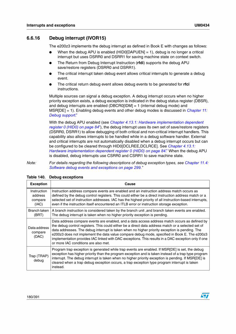
Interrupts and exceptions UM0434
180/391
6.6.16 Debug interrupt (IVOR15)
The e200z3 implements the debug interrupt as defined in Book E with changes as follows:
● When the debug APU is enabled (HID0[DAPUEN] = 1), debug is no longer a critical interrupt but uses DSRR0 and DSRR1 for saving machine state on context switch.
● The Return from Debug Interrupt Instruction (rfdi) supports the debug APU save/restore registers (DSRR0 and DSRR1).
● The critical interrupt taken debug event allows critical interrupts to generate a debug event.
● The critical return debug event allows debug events to be generated for rfci instructions.
Multiple sources can signal a debug exception. A debug interrupt occurs when no higher priority exception exists, a debug exception is indicated in the debug status register (DBSR), and debug interrupts are enabled (DBCR0[IDM] = 1 (internal debug mode) and MSR[DE] = 1). Enabling debug events and other debug modes is discussed in Chapter 11: Debug support.”
With the debug APU enabled (see Chapter 4.13.1: Hardware implementation dependent register 0 (HID0) on page 84”), the debug interrupt uses its own set of save/restore registers (DSRR0, DSRR1) to allow debugging of both critical and non-critical interrupt handlers. This capability also allows interrupts to be handled while in a debug software handler. External and critical interrupts are not automatically disabled when a debug interrupt occurs but can be configured to be cleared through HID0[DCLREE,DCLRCE]. See Chapter 4.13.1: Hardware implementation dependent register 0 (HID0) on page 84.” When the debug APU is disabled, debug interrupts use CSRR0 and CSRR1 to save machine state.
Note: For details regarding the following descriptions of debug exception types, see Chapter 11.4: Software debug events and exceptions on page 299.”
Table 140. Debug exceptions
Exception Cause
Instruction address compare
(IAC)
Instruction address compare events are enabled and an instruction address match occurs as defined by the debug control registers. This could either be a direct instruction address match or a selected set of instruction addresses. IAC has the highest priority of all instruction-based interrupts, even if the instruction itself encountered an ITLB error or instruction storage exception.
Branch taken (BRT)
A branch instruction is considered taken by the branch unit ,and branch taken events are enabled. The debug interrupt is taken when no higher priority exception is pending.
Data address compare
(DAC)
Data address compare events are enabled, and a data access address match occurs as defined by the debug control registers. This could either be a direct data address match or a selected set of data addresses. The debug interrupt is taken when no higher priority exception is pending. The e200z3 does not implement the data value compare debug mode, specified in Book E. The e200z3 implementation provides IAC linked with DAC exceptions. This results in a DAC exception only if one or more IAC conditions are also met.
Trap (TRAP) debug
Program trap exception is generated while trap events are enabled. If MSR[DE] is set, the debug exception has higher priority than the program exception and is taken instead of a trap type program interrupt. The debug interrupt is taken when no higher priority exception is pending. If MSR[DE] is cleared when a trap debug exception occurs, a trap exception type program interrupt is taken instead.

UM0434 Interrupts and exceptions
181/391
The DBSR provides a syndrome to differentiate among debug exceptions that can generate the same interrupt. Table 141 lists register settings when a debug interrupt is taken.
Return (RET)
Return exceptions are enabled and rfi is executed. Return debug exceptions are not generated for rfci or rfdi. If MSR[DE] = 1 when rfi executes, a debug interrupt occurs if no higher priority, enabled exception exists. CSRR0 (debug APU disabled) or DSRR0 (debug APU enabled) is to set the address of the rfi. If MSR[DE] = 0 when rfi executes, a debug interrupt does not occur immediately; the event is recorded by setting DBSR[RET] and DBSR[IDE].
Critical return (CRET)
Critical return debug events are enabled and rfci is executed. Critical return debug exceptions are only generated for rfci. If MSR[DE]=1 when rfci executes, a debug interrupt occurs if no higher priority exception exists that is enabled to cause an interrupt. CSRR0 (debug APU disabled) or DSRR0 (debug APU enabled) is set to the address of the rfci. If MSR[DE] = 0 when rfci executes, a debug interrupt does not occur immediately, but the event is recorded by setting DBSR[CRET] and DBSR[IDE]. Note that critical return debug events should not normally be enabled unless the debug APU is enabled to avoid corrupting CSRR0 and CSRR1.
Instruction complete (ICMP)
An instruction completed while this event is enabled. A mtmsr or mtdbcr0 that causes both MSR[DE] and DBCR0[IDM] to end up set, enabling precise debug mode, may cause an imprecise (delayed) debug exception to be generated due to an earlier recorded event in the DBSR.
Interrupt taken (IRPT)
A non-critical interrupt context switch is detected. This exception is imprecise and unordered with respect to the program flow. Note that an IRPT debug interrupt occurs only when detecting a non-critical interrupt on the e200z3. The value saved in CSRR0/DSRR0 is the address of the non-critical interrupt handler.
Critical interrupt
taken (CIRPT)
A critical interrupt context switch is detected. This exception is imprecise and unordered with respect to program flow. Note that a CIRPT debug interrupt occurs only when detecting a critical interrupt on the e200z3. The address of the critical interrupt handler is saved in CSRR0/DSRR0. To avoid corrupting CSRR0 and CSRR1, critical interrupt taken debug events should not normally be enabled unless the debug APU is enabled.
Unconditional debug event
(UDE) The unconditional debug event signal (p_ude) transitions to asserted state.
Debug counter
A debug counter exception is enabled and a debug counter decrements to zero.
External debug
An external debug exception is enabled and an external debug event (p_devt1, p_devt2) transitions to the asserted state.
Table 140. Debug exceptions (continued)
Exception Cause
Table 141. Debug interrupt register settings
Register Setting description
CSRR0 (MSR[DE]=0)
DSRR0(1) (MSR[DE]=1)
Set to the effective address of the excepting instruction for IAC, BRT, RET, CRET, and TRAP.
Set to the effective address of the next instruction to be executed following the excepting instruction for DAC and ICMP.
For UDE, IRPT, CIRPT, DCNT, or DEVT type exceptions, set to the effective address of the instruction that would have attempted to execute next if no exception conditions were present.
CSRR1/ DSRR1 Set to the contents of the MSR at the time of the interrupt
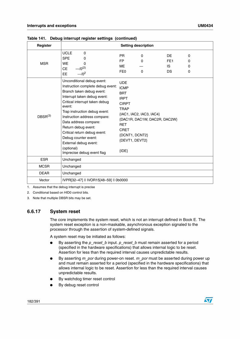
Interrupts and exceptions UM0434
182/391
6.6.17 System reset
The core implements the system reset, which is not an interrupt defined in Book E. The system reset exception is a non-maskable, asynchronous exception signaled to the processor through the assertion of system-defined signals.
A system reset may be initiated as follows:
● By asserting the p_reset_b input. p_reset_b must remain asserted for a period (specified in the hardware specifications) that allows internal logic to be reset. Assertion for less than the required interval causes unpredictable results.
● By asserting m_por during power-on reset. m_por must be asserted during power up and must remain asserted for a period (specified in the hardware specifications) that allows internal logic to be reset. Assertion for less than the required interval causes unpredictable results.
● By watchdog timer reset control
● By debug reset control
MSR
UCLE 0
SPE 0
WE 0CE —/0(2)
EE —/02
PR 0FP 0
ME —
FE0 0
DE 0FE1 0
IS 0
DS 0
DBSR(3)
Unconditional debug event:
Instruction complete debug event:
Branch taken debug event:Interrupt taken debug event:
Critical interrupt taken debug event:
Trap instruction debug event:
Instruction address compare:Data address compare:
Return debug event:
Critical return debug event:
Debug counter event:External debug event:
(optional) Imprecise debug event flag
UDE
ICMP
BRTIRPT
CIRPT
TRAP{IAC1, IAC2, IAC3, IAC4}
{DAC1R, DAC1W, DAC2R, DAC2W}
RET
CRET{DCNT1, DCNT2}
{DEVT1, DEVT2}
{IDE}
ESR Unchanged
MCSR Unchanged
DEAR Unchanged
Vector IVPR[32–47] || IVOR15[48–59] || 0b0000
1. Assumes that the debug interrupt is precise
2. Conditional based on HID0 control bits.
3. Note that multiple DBSR bits may be set.
Table 141. Debug interrupt register settings (continued)
Register Setting description

UM0434 Interrupts and exceptions
183/391
When a reset request occurs, the processor branches to the system reset exception vector (value on p_rstbase[0:19] concatenated with 0xFFC) without attempting to reach a recoverable state. If reset occurs during normal operation, all operations stop and machine state is lost. The internal state of the e200z6e200z3 after a reset is defined in Chapter 4.18.4: Reset settings.”
For reset initiated by watchdog timer or debug reset control, the e200z6 implements TSR[WRS] or DBSR[MRR] to help software determine the cause. Watchdog timer and debug reset control provide the capability to assert p_resetout_b. External logic may factor this signal into p_reset_b to cause an e200z6e200z3 reset.
Table 142 shows the TSR bits associated with reset status.
Table 143 shows the DBSR bits associated with reset status.
Table 144 lists register settings when a system reset is taken.
6.6.18 SPE APU unavailable interrupt (IVOR32)
The SPE APU unavailable exception is taken if MSR[SPE] is cleared and execution of an SPE APU instruction other than an embedded scalar floating-point or brinc instruction is attempted. When the SPE APU unavailable exception occurs, the processor suppresses
Table 142. TSR watchdog timer reset status
Bits Name Description
34–35 WRS
00 No action performed by watchdog timer
01 Watchdog timer second timeout caused checkstop.
10 Watchdog timer second timeout caused p_resetout_b to be asserted.
11 Reserved
Table 143. DBSR most recent reset
Bits Name Function
34–35 MRR00 No reset occurred since these bits were last cleared by software.01 A reset occurred since these bits were last cleared by software.
1x Reserved
Table 144. System reset register Settings
Register Setting description
CSRR0 Undefined
CSRR1 Undefined
MSR
UCLE 0
WE 0CE 0
EE 0PR 0
FP 0
ME 0
DE 0FE1 0
IS 0
DS 0
ESR Cleared
DEAR Undefined
Vector [p_rstbase[0:19]] || 0xFFC

Interrupts and exceptions UM0434
184/391
execution of the instruction causing the exception. Table 145 lists register settings when an SPE unavailable interrupt is taken.
6.6.19 SPE Floating-Point data interrupt (IVOR33)
The SPE floating-point data interrupt is taken if no higher priority exception exists and an SPE floating-point data exception is generated. When a floating-point data exception occurs, the processor suppresses execution of the instruction causing the exception.
Table 146 lists register settings when an SPE floating-point data interrupt is taken.
Table 145. SPE unavailable interrupt register settings
Register Setting description
SRR0 Set to the effective address of the excepting SPE instruction
SRR1 Set to the contents of the MSR at the time of the interrupt
MSR
UCLE 0
SPE 0WE 0
CE —
EE 0
PR 0
FP 0
ME —FE0 0
DE —
FE1 0
IS 0DS 0
ESR SPE, [VLEMI]. All other bits cleared.
MCSR Unchanged
DEAR Unchanged
Vector IVPR[32–47] || IVOR32[48–59] || 0b0000
Table 146. SPE Floating-Point data interrupt register settings
Register Setting description
SRR0 Set to the effective address of the excepting SPE instruction.
SRR1 Set to the contents of the MSR at the time of the interrupt
MSR
UCLE 0
SPE 0
WE 0CE —
EE 0
PR 0FP 0
ME —
FE0 0
DE —FE1 0
IS 0
DS 0
ESR SPE, [VLEMI]. All other bits cleared.
MCSR Unchanged
DEAR Unchanged
Vector IVPR[32–47] || IVOR33[48–59] || 0b0000

UM0434 Interrupts and exceptions
185/391
6.6.20 SPE Floating-Point round interrupt (IVOR34)
The SPE floating-point round interrupt is taken when an SPE floating-point instruction generates an inexact result and inexact exceptions are enabled.
Table 147 lists register settings when an SPE floating-point round interrupt is taken.
6.7 Exception recognition and prioritiesThe following list of exception categories describes how the e200z3 handles exceptions up to the point of signaling the appropriate interrupt to occur. Also, instruction completion is defined as updating all architectural registers associated with that instruction as necessary, and then removing the instruction from the pipeline.
● Interrupts caused by asynchronous events (exceptions). These exceptions are further distinguished by whether they are maskable and recoverable.
– Asynchronous, non-maskable, non-recoverable: System reset by assertion of p_reset_b. Has highest priority and is taken immediately regardless of other pending exceptions or recoverability. (Includes watchdog timer reset control and debug reset control)
– Asynchronous, maskable, non-recoverable: Machine check interrupt.
Has priority over any other pending exception except system reset conditions; is dependent on the source of the exception. Typically non-recoverable.
– Asynchronous, maskable, recoverable: External input, fixed-interval timer, decrementer, critical input, unconditional debug, external debug event, debug counter event, and watchdog timer interrupts.
Before handling this type of exception, the processor needs to reach a recoverable state. A maskable recoverable exception remains pending until taken or cancelled by software.
Table 147. SPE Floating-Point round interrupt register settings
Register Setting description
SRR0 Set to the effective address of the instruction following the excepting SPE instruction.
SRR1 Set to the contents of the MSR at the time of the interrupt
MSR
UCLE 0
SPE 0WE 0
CE —
EE 0
PR 0
FP 0
ME —FE0 0
DE —
FE1 0
IS 0DS 0
ESR SPE, [VLEMI]. All other bits cleared.
MCSR Unchanged
DEAR Unchanged
Vector IVPR[32–47] || IVOR34[48–59] || 0b0000

Interrupts and exceptions UM0434
186/391
● Synchronous, non-instruction-based interrupts. The only exception in this category is the interrupt taken debug exception, recognized by an interrupt taken event. It is not considered instruction-based but is synchronous with respect to program flow.
– Synchronous, maskable, recoverable: Interrupt taken debug event. The machine is in a recoverable state due to the state of the machine at the context switch triggering this event.
● Instruction-based interrupts. These interrupts are further organized by the point in instruction processing in which they generate an exception.
– Instruction fetch: Instruction storage, instruction TLB, and instruction address compare debug exceptions.
Once these types of exceptions are detected, the excepting instruction is tagged. When the excepting instruction is next to begin execution and a recoverable state has been reached, the interrupt is taken. If an event prior to the excepting instruction causes a redirection of execution, the instruction fetch exception is discarded (but may be encountered again).
– Instruction dispatch/execution: Program, system call, data storage, alignment, floating-point unavailable, SPE unavailable, data TLB, SPE floating-point data, SPE floating-point round, debug (trap, branch taken, return) interrupts.
Determined during decode or execution of an instruction. The exception remains pending until all instructions before the exception-causing instruction complete. The interrupt is then taken without completing the exception-causing instruction. If completing previous instructions causes an exception, that exception takes priority over the pending instruction dispatch/execution exception, which is discarded (but may be encountered again when instruction processing resumes).
– Post-instruction execution: Debug (data address compare, instruction complete) interrupt
Generated following execution and completion of an instruction while the event is enabled. If executing the instruction produces conditions for another type of exception with higher priority, that exception is taken and the post-instruction exception is discarded for the instruction (but may be encountered again when instruction processing resumes).
6.7.1 Interrupt priorities
Interrupts are prioritized as described in Table 148. Some exceptions may be masked or imprecise, which affects their priority. Non-maskable exceptions such as reset and machine check may occur at any time and are not delayed even if an interrupt is being serviced; thus, state information for any interrupt may be lost. Reset and most machine checks are non-recoverable.
Table 148. e200z3 exception priorities
Priority Exception Cause IVOR
Asynchronous exceptions
System resetAssertion of p_reset_b, watchdog timer reset control, or debug reset control
none
Machine checkAssertion of p_mcp_b, exception on fetch of first instruction of an interrupt handler, bus error on buffered store , bus error (XTE) with MSR[EE]=0 and current MSR[ME]=1
1

UM0434 Interrupts and exceptions
187/391
— — —
(1)
Debug: UDEDebug: DEVT1
Debug: DEVT2
Debug: DCNT1Debug: DCNT2
Debug: IDE
Assertion of p_ude (unconditional debug event)Assertion of p_devt1 and event enabled (external debug event 1)Assertion of p_devt2 and event enabled (external debug event 2)Debug counter 1 exception
Debug counter 2 exception
Imprecise debug event (event imprecise due to earlier, higher priority interrupt
15
1 Critical Input Assertion of p_critint_b 0
1 Watchdog timer Watchdog timer first enabled time-out 12
1 External input Assertion of p_extint_b 4
1 Fixed-interval timerPosting of a fixed-interval timer exception in TSR due to programmer-specified bit transition in the time base register
11
1 DecrementerPosting of a decrementer exception in TSR due to programmer-specified decrementer condition
10
Instruction fetch exceptions
Debug: IAC (unlinked)
Instruction address compare match for enabled IAC debug event and DBCR0[IDM] asserted
15
ITLB error Instruction translation lookup miss in the TLB 14
Instruction storage
Access control
Precise external termination error (p_tea_b assertion and precise recognition) and MSR[EE] = 1
Byte ordering due to misaligned instruction across page boundary to pages with mismatched VLE bits, or access to page with VLE set and E indicating little-endian.
Misaligned Instruction fetch due to a change of flow to an odd halfword instruction boundary on a BookE (non-VLE) instruction page, due to value in LR, CTR, or xSRR0
3
Instruction dispatch/execution interrupts
Program: Illegal Attempted execution of an illegal instruction 6
Program: privileged Attempted execution of a privileged instruction in user mode 6
Floating-point unavailable
Any floating-point unavailable exception condition 7
SPE unavailable Any SPE unavailable exception condition 32
Program: unimplemented
Attempted execution of an unimplemented instruction 6
Table 148. e200z3 exception priorities (continued)
Priority Exception Cause IVOR

Interrupts and exceptions UM0434
188/391
Debug: BRT
Debug: Trap
Debug: RETDebug: CRET
Attempted execution of a taken branch instruction
Condition specified in tw or twi instruction met.
Attempted execution of a rfi instructionAttempted execution of an rfci instruction
Exceptions require corresponding debug event enabled, MSR[DE]=1, and DBCR0[IDM]=1.
15
Program: trapCondition specified in tw or twi instruction met and not a debug trap exception
15
System call Execution of the system call (sc, se_sc) instruction. 8
SPE floating-point data
NaN, infinity, or denormalized data detected as input or output, or underflow, overflow, divide by zero, or invalid operation in the SPE APU.
33
SPE round Inexact result 34
Alignmentlmw, stmw, lwarx, or stwcx. Not word aligned. dcbz with cache disabled or not present
5
Debug with concurrent DTLB or data storage interrupt:
DAC/IAC linked(2)
DAC unlinked2
Debug with concurrent DTLB or data storage interrupt. DBSR[IDE] also set.
Data address compare linked with instruction address compare
Data address compare unlinked
Note: Exceptions require corresponding debug event enabled, MSR[DE]=1, and DBCR0[IDM]=1. In this case, the debug exception is considered imprecise and DBSR[IDE] is set. Saved PC points to the load or store instruction causing the DAC event.
15
Data TLB error Data translation lookup miss in the TLB. 13
Data storage
Access control.Byte ordering due to misaligned access across page boundary to pages with mismatched E bits.Precise external termination error (p_tea_b assertion and precise recognition) and MSR[EE]=1
2
Debug: IRPT
Debug: CIRPT
Interrupt taken (non-critical)
Critical interrupt taken (critical only)Note: Exceptions require corresponding debug event enabled, MSR[DE]=1 and DBCR0[IDM]=1.
15
Table 148. e200z3 exception priorities (continued)
Priority Exception Cause IVOR

UM0434 Interrupts and exceptions
189/391
6.8 Interrupt processingWhen an interrupt is taken, SRR0/SRR1 for non-critical interrupts, CSRR0/CSRR1 for critical interrupts, and either CSRR0/CSRR1 or DSRR0/DSRR1 for debug interrupts are used to save the contents of the MSR and to help identify where instruction execution should resume after the interrupt is handled.
When an interrupt occurs, one of SRR0/CSRR0/DSRR0 is set to the address of the instruction that caused the exception or to the following instruction if appropriate.
SRR1 is used to save machine state (selected MSR bits) on non-critical interrupts and to restore those values when an rfi executes. CSRR1 is used to save machine status (selected MSR bits) on critical interrupts and to restore those values when an rfci instruction is executed. DSRR1 is used to save machine status (selected MSR bits) on debug interrupts when the debug APU is enabled and to restore those values when an rfdi executes.
The ESR is loaded with information specific to the exception type. Some interrupt types can only be caused by a single exception type and thus do not use an ESR setting to indicate the interrupt cause.
The MSR is updated to preclude unrecoverable interrupts from occurring during the initial portion of the interrupt handler. Specific settings are described in Table 149.
For alignment, data storage, or data TLB miss interrupts, or for a machine check due to cache parity error on data access interrupts, the data exception address register (DEAR) is loaded with the address that caused the interrupt to occur.
For machine check interrupts, the MCSR is loaded with information specific to the exception type.
Post-instruction execution exceptions
Debug: DAC/IAC linked2
Debug: DAC unlinked2
Data address compare linked with instruction address compareData address compare unlinked
Notes:
Exceptions require corresponding debug event enabled, MSR[DE] = 1 and DBCR0[IDM] = 1.
Saved PC points to the instruction following the load or store instruction causing the DAC event.
15
Debug: ICMPCompletion of an instruction.
Note: Exceptions require corresponding debug event enabled, MSR[DE]=1, and DBCR0[IDM]=1.
15
1. These exceptions are sampled at instruction boundaries, and may actually occur after exceptions that are due to a currently executing instruction. If one of these exceptions occurs during execution of an instruction in the pipeline, it is not processed until the pipeline has been flushed, and the exception associated with the excepting instruction may occur first.
2. When no data storage interrupt or data TLB error occurs, the core implements the data address compare debug exceptions as post-instruction exceptions, which differs from the Book E definition. When a TEA (either a DTLB error or data storage interrupt) occurs in conjunction with an enabled DAC or linked DAC/IAC on a load or store class instruction, the debug interrupt takes priority, and the saved PC value points to the load or store class instruction, rather than to the next instruction.
Table 148. e200z3 exception priorities (continued)
Priority Exception Cause IVOR

Interrupts and exceptions UM0434
190/391
Instruction fetch and execution resume, using the new MSR value, at a location specific to the exception type. The location is determined by the IVPR and an IVOR specific for each type of interrupt (see Table 114). A new operating context is selected using the low-order three bits of the specific IVOR selected by the type of interrupt.
Table 149 shows the MSR settings for different interrupt categories. Note that reserved and preserved MSR bits are unimplemented and are read as 0.
6.8.1 Enabling and disabling exceptions
When a condition exists that may cause an exception to be generated, it must be determined whether the exception is enabled for that condition.
● System reset exceptions cannot be masked.
● A machine check exception can occur only if the machine check enable, MSR[ME], = 1. If ME = 0, the processor goes directly into checkstop state when a machine check exception condition occurs. Individual machine check exceptions can be enabled and disabled through HID0 bits.
● Asynchronous, maskable non-critical exceptions (such as the external input and decrementer) are enabled by setting MSR[EE]. When EE = 0, recognition of these exception conditions is delayed. EE is cleared automatically when a non-critical or critical interrupt is taken to mask further recognition of conditions causing those exceptions.
● Asynchronous, maskable critical exceptions (such as critical input and watchdog timer) are enabled by setting MSR[CE]. When CE = 0, recognition of these exception conditions is delayed. CE is cleared automatically when a critical interrupt is taken to mask further recognition of conditions causing those exceptions.
● Synchronous and asynchronous debug exceptions are enabled by setting MSR[DE]. If DE = 0, recognition of these exception conditions is masked. DE is cleared
Table 149. MSR setting due to interrupt
Bits MSR definition Reset setting Non-critical interrupt Critical interrupt Debug interrupt
37 UCLE 0 0 0 0
38 SPE 0 0 0 0
45 WE 0 0 0 0
46 CE 0 — 0 —/0(1)
1. Conditionally cleared based on control bits in HID0
48 EE 0 0 0 —/01
49 PR 0 0 0 0
50 FP 0 0 0 0
51 ME 0 — — —
52 FE0 0 0 0 0
54 DE 0 — —/01 0
55 FE1 0 0 0 0
58 IS 0 0 0 0
59 DS 0 0 0 0

UM0434 Interrupts and exceptions
191/391
automatically when a debug interrupt is taken to mask further recognition of conditions causing those exceptions. Chapter 11: Debug support,” gives details on individual control of debug exceptions.
● The floating-point unavailable exception can be prevented by setting MSR[FP] (although the e200z3 generates an unimplemented instruction exception instead).
6.8.2 Returning from an interrupt handler
The Return from Interrupt (rfi), Return from Critical Interrupt (rfci) and Return from Debug Interrupt (rfdi) instructions perform context synchronization by allowing instructions issued earlier to complete before returning to the interrupted process. In general, execution of rfi, rfci, or rfdi ensures the following:
● All previous instructions have completed to a point where they can no longer cause an exception. This includes post-execute type exceptions.
● Previous instructions complete execution in the context (privilege and protection) under which they were issued.
● The rfi copies SRR1 bits back into the MSR.
● The rfci copies CSRR1 bits back into the MSR.
● The rfdi copies DSRR1 bits back into the MSR.
● Instructions fetched after this execution in the context established by this instruction.
● Program execution resumes at the instruction indicated by SRR0 for rfi, CSRR0 for rfci or DSRR0 for rfdi.
Note that the rfi may be subject to a return type debug exception and that rfci may be subject to a critical return type debug exception. For a complete description of context synchronization, refer to the EREF.
6.9 Process switchingThe following instructions are useful for restoring proper context during process switching:
● msync orders the effects of data memory instruction execution. All instructions previously initiated appear to have completed before the msync instruction completes, and no subsequent instructions appear to be initiated until the msync instruction completes.
● isync waits for all previous instructions to complete and then discards any fetched instructions, causing subsequent instructions to be fetched (or refetched) from memory and to execute in the context (privilege, translation, and protection) established by the previous instructions.
● stwcx. clears any outstanding reservations, ensuring that a load and reserve instruction in an old process is not paired with a store conditional instruction in a new one.

Memory management unit UM0434
192/391
7 Memory management unit
This chapter describes the implementation details of the e200z3 core complex MMU relative to the Book E architecture and the Freescale Book E standards.
7.1 OverviewThe e200z3 memory management unit is a 32-bit PowerPC Book E–compliant implementation.
7.1.1 MMU features
The MMU of the e200z3 core has the following feature set:
● Freescale Book E implementation standard (EIS) MMU architecture compliant
● 32-bit effective address translated to 32-bit real address (using a 41-bit interim virtual address)
● 16-entry, fully associative, translation lookaside buffer (TLB1) that supports the nine page sizes (4 Kbytes, 16 Kbytes, 64 Kbytes, 256 Kbytes, 1 Mbyte, 4 Mbytes, 16 Mbytes, 64 Mbytes, 256 Mbytes), shown in Table 151
● One 32-bit PID register (PID0) for supporting up to 255 translation IDs at any time in the TLB
● No page table format defined; software is free to use its own page table format
● Hardware assist for TLB miss exceptions
● TLB1 managed by tlbre, tlbwe, tlbsx, tlbsync, and tlbivax instructions and six MMU assist (MAS) registers
● IPROT bit implemented in TLB1 prevents invalidations, protecting critical entries (so designated by having the IPROT bit set) from being invalidated.
7.1.2 TLB entry maintenance features summary
The TLB entries of the e200z3 core complex must be loaded and maintained by the system software; this includes performing any required table search operations in memory. The e200z3 provides support for maintaining TLB entries in software with the resources shown in Table 150. Note that many of these features are defined at the Freescale Book E level.

UM0434 Memory management unit
193/391
Other hardware assistance features for maintenance of the TLB on the e200z3 are described in Chapter : MAS register updates on page 205.”
7.2 Effective to real address translationThis section describes the general principles that guide the PowerPC Book E definition for memory management and further describes the structure for MMUs defined by the Freescale Book E implementation standard (EIS) and the e200z3 MMU.
Figure 7 shows the high-level translation flow, showing that because the smallest page size supported by the e200z3 core complex is 4 Kbytes, the 12 lsbs always index within the page and are untranslated.
Table 150. TLB maintenance programming model
Features Description Section/page
TLB Instructions
tlbre TLB Read Entry instructionChapter 7.4 on
page 200
tlbwe TLB Write Entry instructionChapter 7.4 on
page 200
tlbsx rA, rB TLB Search for Entry instructionChapter 7.4 on
page 200
tlbivax rA, rB TLB Invalidate Entries instructionChapter 7.4 on
page 200
tlbsyncTLB Synchronize Invalidations with other masters’ instruction (privileged no-op on the e200z3)
Chapter 7.4 on page 200
Registers
PID0 Process ID registerChapter 4.4.2 on page 45
MMUCSR0 MMU control and status registerChapter 4.16.1
on page 88
MMUCFG MMU configuration registerChapter 4.16.2
on page 89
TLB0CFG–TLB1CFG TLB configuration registersChapter 4.16.3
on page 90
MAS0–MAS4, MAS6MMU assist registers. Note: e200z3 does not implement MAS5.
Chapter 4.16.4 on page 91
DEAR Data exception address registerChapter on
page 57
Interrupts
Instruction TLB miss exception
Causes instruction TLB error interruptChapter 6.6.15 on page 179
Data TLB miss exception Causes data TLB error interruptChapter 6.6.14 on page 179
Instruction permission violation exception
Causes ISI interruptChapter 6.6.4 on page 172
Data permission violation exception
Causes DSI interruptChapter 6.6.3 on page 171

Memory management unit UM0434
194/391
Figure 7. Effective to real address translation flow
32-Bit Effective Address
32-Bit Real Address
Virtual Address
NOTE: n = 32–log2 (page size)n> = 20n = 20 for 4-Kbyte page size
PID Effective Page Address Offset
0 n 31
TLB Multiple-Entry
MSR[IS] for Instruction Fetch
AS
MSR[DS] for Data Access
RPN field of matching entry
n–1
Real Page Number Offset
0 n 31n–1
Effective Page Number Byte Address
Real Page Number Byte Address
32-bit Effective Address (EA)
32-Bit Real Address
15–20 Bits* >12 Bits*
15–20 Bits* >12 Bits*
MMU (Unified)
Three 41-Bit Virtual Addresses (VAs)
8 Bits
MSR··· IS DS ···
Instruction Access
Data Access
AS PID0
* Number of bits depends on page size(4 Kbytes–128 Mbytes)
32-Entry Fully–Assoc. VSP Array (TLB1)MAS Registers

UM0434 Memory management unit
195/391
7.2.1 Effective addresses
Instruction accesses are generated by sequential instruction fetches or due to a change in program flow (branches and interrupts). Data accesses are generated by load, store, and cache management instructions. The e200z3 instruction fetch, branch, and load/store units generate 32-bit effective addresses. The MMU translates these effective addresses to 32-bit physical (real) addresses that are then used for memory accesses.
The PowerPC Book E architecture divides the effective (virtual) and real (physical) address space into pages. The page represents the granularity of effective address translation, permission control, and memory/cache attributes. The e200z3 MMU supports nine page sizes (4 Kbytes to 256 Mbytes, as defined in Table 151). In order for an effective-to-real address translation to exist, a valid entry for the page containing the effective address must be in a TLB. Accesses to addresses for which no TLB entry exists (a TLB miss) cause instruction or data TLB errors.
7.2.2 Address spaces
The PowerPC Book E architecture defines two effective address spaces for instruction accesses and two effective address spaces for data accesses. The current effective address space for instruction or data accesses is determined by the value of MSR[IS] (instruction address space bit) and MSR[DS] (data address space bit), respectively. The address space indicator (the corresponding value of either MSR[IS] or MSR[DS]) is used in addition to the effective address generated by the processor for translation into a physical address by the TLB mechanism. Because MSR[IS] and MSR[DS] are both cleared when an interrupt occurs, an address space value of 0 can be used to denote interrupt-related address spaces (or possibly all system software address spaces). An address space value of 1 can be used to denote non–interrupt-related address spaces or possibly all user address spaces.
The address space associated with an instruction or data access is included as part of the virtual address in the translation process (AS).
7.2.3 Virtual addresses and process ID
The PowerPC Book E architecture requires a process ID (PID) value to be associated with each effective address (instruction or data) generated by the processor to construct a virtual address for each access. At the Book E level, a single PID register is defined as a 32-bit register, and it maintains the value of the PID for the current process. This PID value is included as part of the virtual address in the translation process (PID0).
For the e200z3 MMU, the PID is 8 bits in length. The most significant 24 bits are unimplemented and read as 0. The p_pid0[0:7] interface signals indicate the current process ID.
The core complex implements a single process ID (PID) register, PID0, as an SPR shown in Chapter 4.16.5 on page 96.” The current value in the PID register is used in the TLB look-up process and compared with the TID field in all the TLB entries. If the PID value in PID0 matches with a TLB entry in which all the other match criteria are met, that entry is used for translation.
Note that when a TID value in a TLB entry is all zeros, it always causes a match in the PID compare (effectively ignoring the values of the PID register). Thus, the operating system can set the values of all the TIDs to zero, effectively eliminating the PID value from all translation comparisons.

Memory management unit UM0434
196/391
7.2.4 Translation flow
The effective address, concatenated with the address space value of the corresponding MSR bit (MSR[IS] or MSR[DS]), is compared to the appropriate number of bits of the EPN field (depending on the page size) and the TS field of TLB entries. If the contents of the effective address plus the address space bit matches the EPN field and TS bit of the TLB entry, that TLB entry is a candidate for a possible translation match. In addition to a match in the EPN field and TS, a matching TLB entry must match with the current process ID of the access (in PID0), or have a TID value of 0, indicating that the entry is globally shared among all processes.
Figure 8 shows the translation match logic for the effective address plus its attributes, collectively called the virtual address, and how it is compared with the corresponding fields in the TLB entries.
Figure 8. Virtual address and TLB-Entry compare process
The page size defined for a TLB entry determines how many bits of the effective address are compared with the corresponding EPN field in the TLB entry as shown in Table 151. On a TLB hit, the corresponding bits of the real page number (RPN) field are used to form the real address, and the generation of the physical address occurs as shown in Figure 7.
Table 151. Page size (for e200z3 Core) and EPN field comparison
SIZE FieldPage Size
(4SIZE Kbytes)EA to EPN Comparison
(Bits 32–53; 2 × SIZE)
0b0001 4 Kbytes EA[32–51] = EPN[32–51]?
0b0010 16 Kbytes EA[32–49] = EPN[0–49]?
0b0011 64 Kbytes EA[32–47] = EPN[32–47]?
0b0100 256 Kbytes EA[32–45] = EPN[32–45]?
0b0101 1 Mbyte EA[32–43] = EPN[32–43]?
0b0110 4 Mbytes EA[32–41] = EPN[32–41]?
0b0111 16 Mbytes EA[32–39] = EPN[32–39]?
0b1000 64 Mbytes EA[32–37] = EPN[32–37]?
0b1001 256 Mbytes EA[32–35] = EPN[32–35]?
TLB Entry Hit
=0?
Private Page
Shared Pagee
=?
=?
TLB_entry[V]
TLB_entry[TS]
TLB_entry[TID]
TLB_entry[EPN]
AS (from MSR[IS] or MSR[DS])
Process ID
EA Page Number Bits
=?

UM0434 Memory management unit
197/391
7.2.5 Permissions
An operating system may restrict access to virtual pages by selectively granting permissions for user-mode read, write, and execute, and supervisor-mode read, write, and execute on a per-page basis. These permissions can be set up for a particular system (for example, program code may be execute only, and data structures may be mapped as read/write/no-execute) and be changed by the operating system based on application requests and operating system policies.
The UX, SX, UW, SW, UR, and SR access control bits are provided to support selective permissions (access control):
● SR—Supervisor read permission. Allows loads and load-type cache management instructions to access the page while in supervisor mode (MSR[PR = 0]).
● SW—Supervisor write permission. Allows stores and store-type cache management instructions to access the page while in supervisor mode (MSR[PR = 0]).
● SX—Supervisor execute permission. Allows instruction fetches to access the page and instructions to be executed from the page while in supervisor mode (MSR[PR = 0]).
● UR—User read permission. Allows loads and load-type cache management instructions to access the page while in user mode (MSR[PR = 1]).
● UW—User write permission. Allows stores and store-type cache management instructions to access the page while in user mode (MSR[PR = 1]).
● UX—User execute permission. Allows instruction fetches to access the page and instructions to be executed from the page while in user mode (MSR[PR = 1]).
If the translation match was successful, the permission bits are checked as shown in Figure 9. If the access is not allowed by the access permission mechanism, the processor generates an instruction or data storage interrupt (ISI or DSI).
Figure 9. Granting of access permission
7.3 Translation lookaside bufferThe EIS architecture defines support for zero or more TLBs in an implementation, each with its own characteristics, and provides configuration information for software to query the existence and structure of TLBs through a set of SPRs—MMUCFG, TLB0CFG, TLB1CFG, and so on. By convention, TLB0 is used for a set-associative TLB with fixed page sizes,
Access Granted
Instruction FetchMSR[PR]
TLB_entry[UX]
TLB_entry[SX]
TLB_entry[UR]
TLB_entry[SR]
TLB_entry[UW]
TLB_entry[SW]
Load-Class Data Access
Store-Class Data Access
TLB Match (see Figure 5-2)

Memory management unit UM0434
198/391
TLB1 is used for a fully-associative TLB with variable page sizes, and TLB2 is arbitrarily defined by an implementation. The e200z3 MMU supports a single TLB that is fully associative and supports variable page sizes; thus it corresponds to TLB1 in the programming model. For the rest of this document, TLB, TLBCAM, and TLB1 are used interchangeably.
The TLB on the e200z3 MMU (TLB1) consists of a 16-entry, fully-associative content-addressable memory (CAM) array with support for nine page sizes. To perform a lookup, the TLB is searched in parallel for a matching TLB entry. The contents of a matching TLB entry are then concatenated with the page offset of the original effective address. The result constitutes the real (physical) address of the access.
A hit to multiple TLB entries is considered to be a programming error. If this occurs, the TLB generates an invalid address and TLB entries may be corrupted (an exception will not be reported).
The structure of TLB1 is shown in Figure 10.
Figure 10. e200z3 TLB1 organization
7.3.1 IPROT invalidation protection in TLB1
The IPROT bit in TLB1 is used to protect TLB entries from invalidation. TLB1 entries with IPROT set are not invalidated by a tlbivax instruction executed by this processor (even when the INV_ALL command is indicated), or by a flash invalidate initiated by writing to MMUCSR0[TLB1_FI]. The IPROT bit can be used to protect critical code and data such as interrupt vectors/handlers in order to guarantee that the instruction fetch of those vectors never takes a TLB miss exception. Entries with IPROT set can only be invalidated by writing a 0 to the valid bit of the entry (by using the MAS registers and executing the tlbwe instruction).
Invalidation operations generated by execution of the tlbivax instruction are guaranteed to invalidate the entry that translates the address specified in the operand of the tlbivax instruction. Additional entries may also be invalidated by this operation if they are not protected with IPROT. A precise invalidation can be performed by writing a 0 to the valid bit of a TLB entry.
0
15
TLB1
Compare
Compare
RPN Hit
Real Address(translated bits, depending on page size)
Virtual Address

UM0434 Memory management unit
199/391
7.3.2 Replacement algorithm for TLB1
The replacement algorithm for TLB1 must be implemented completely by system software. Thus, when an entry in TLB1 is to be replaced, the software can select which entry to replace and write the entry number to the MAS0[ESEL] field before executing a tlbwe instruction.
Alternately, the software can load the entry number of the next desired victim into MAS0[NV]. The e200z3 then automatically loads MAS0[ESEL] from MAS0[NV] on a TLB error condition as shown in Figure 11.
See Table 156 for a complete description of MAS register updates on various exception conditions.
Figure 11. Victim selection
7.3.3 The G bit (of WIMGE)
The G bit provides protection from bus accesses that could be canceled due to an exception on a prior uncompleted instruction.
If G = 1 (guarded), these types of accesses must stall until the exception status of any instructions in progress is known. If G = 0 (unguarded), these accesses may be issued to the bus regardless of the completion status of other instructions. Because the core does not make requests for load or store instructions until it is known that prior instructions will complete without exceptions, the G bit is essentially ignored. Proper operation always occurs to guarded storage.
7.3.4 TLB entry field summary
Table 152 summarizes the fields of e200z3 TLB entries.
Note: All of these fields are defined at the Freescale Book E level.
MAS0
ESEL
NV
On tlbwe SelectsEntry
TLB Miss (TLB Error Interrupt)
Written by Software
Table 152. TLB entry bit fields for e200z3
Field Description
V Valid bit for entry
TS Translation address space (compared with AS bit of the current access)
TID[0–7] Translation ID (compared with PID0 or TIDZ (all zeros))
EPN[0–19] Effective page number (compared with effective address)

Memory management unit UM0434
200/391
7.4 Software interface and TLB instructionsTLB1 is accessed indirectly through several MMU assist (MAS) registers, which software can write and read with mtspr and mfspr instructions. MAS registers contain information related to reading and writing a given entry within TLB1. Data is read from the TLB into the MAS registers with a tlbre (TLB Read Entry) instruction and is written to the TLB from the MAS registers with a tlbwe (TLB Write Entry) instruction.
Certain fields of the MAS registers are also written by hardware when an instruction TLB error, data TLB error, DSI, or ISI interrupt occurs.
On a TLB error interrupt, the MAS registers are written by hardware with the proper EA, default attributes (TID, WIMGE, permissions, and so on), TLB selection information, and an entry in the TLB to replace. Software manages this entry selection information by updating a replacement entry value during TLB miss handling. Software must provide the correct RPN and permission information in one of the MAS registers before executing a tlbwe instruction.
On taking a DSI or ISI interrupt, hardware updates only the search PID (SPID) and search address space (SAS) fields in the MAS registers, using the contents of PID0 and the corresponding MSR[IS] or MSR[DS] value used when the data or instruction storage interrupt was recognized. During the interrupt handler, software can issue a TLB Search Instruction (tlbsx), which uses the SPID field along with the SAS field, to determine the entry related to the data or instruction storage interrupt. Note that it is possible that the entry that caused the data or instruction storage interrupt no longer exists in the TLB by the time
RPN[0–19] Real page number (translated address)
SIZE[0–3]
Encoded page size0000 Reserved
0001 4 Kbytes
0010 16 Kbytes0011 64 Kbytes
0100 256 Kbytes
0101 1 Mbyte0110 4 Mbytes
0111 16 Mbytes
1000 64 Mbytes1001 256 Mbytes
All others—reserved
SX, SW, SR Supervisor execute, write, and read permission bits
UX, UW, UR User execute, write, and read permission bits
WIMGEMemory/cache attributes (write-through, cache-inhibit, memory coherence required, guarded, endian)
U0–U3 User attribute bits—used only by software
IPROT Invalidation protection
VLE VLE page indicator
Table 152. TLB entry bit fields for e200z3 (continued)
Field Description

UM0434 Memory management unit
201/391
the search occurs if a TLB invalidate or replacement removes the entry between the time the exception is recognized and when the tlbsx is executed.
The supervisor instructions tlbre, tlbwe, tlbsx, tlbivax, and tlbsync are fully described in the EREF.
● TLB Read Entry (tlbre)—Causes contents of the TLB entry specified by MAS0[TLBSEL,ESEL]) to be placed into MAS1–MAS3. Table 156 describes how MAS fields are updated.
● TLB Write Entry (tlbwe)—Causes the contents of certain fields within the MAS1, MAS2, and MAS3 to be written into the TLB entry specified by MAS0[TLBSEL,ESEL]. Table 156 describes how MAS fields are updated.
● TLB Search Indexed (tlbsx)—Updates the MAS registers conditionally based on success or failure of a TLB lookup. The lookup is controlled by an effective address provided by rB as specified in the instruction encoding, and by MAS6[SAS,SPID]. The values placed into MAS0–MAS3 differ depending on the success of the search. Table 156 describes how MAS fields are updated.
● TLB Invalidate (tlbivax)—Invalidates TLB entries that correspond to the virtual address calculated by this instruction. The address is detailed in Table 153. No other information except for that shown in Table 153 is used for the invalidation (AS and TID values are ignored).
Additional information about the targeted TLB entries is encoded in two of the lower bits of the effective address calculated by the tlbivax.
EA[0–19] are used to perform the tlbivax invalidation of TLB1.
t
● TLB Synchronize (tlbsync)—Treated as a privileged no-op by the e200z3.
7.5 TLB operationsThis section describes how the software (with some hardware assistance) maintains TLB1.
Table 153. tlbivax EA bit definitions
Bits Field
0–19 EA[0–19]
20–27 Reserved(1)
1. These bits should be zero for future compatibility. They are ignored.
28TLBSEL (1 = TLB1). Should be set, for future compatibility and to ensure that TLB1 is targeted by the invalidate.
29INV_ALL. If set, indicates that the invalidate operation needs to completely invalidate all TLB1 entries that are not marked as invalidation protected (IPROT = 1)
30–31 Reserved 1

Memory management unit UM0434
202/391
7.5.1 Translation reload
The TLB reload function is performed in software with some hardware assistance. This hardware assistance consists of the following:
● Five 32-bit MMU assist registers (MAS0–MAS4, MAS6) for support of the tlbre, tlbwe, and tlbsx TLB management instructions.
● Loading of MAS0–MAS2 based upon defaults in MAS4 for TLB miss exceptions. This automatically generates most of the TLB entry.
● Loading of the data exception address register (DEAR) with the EA of the load, store, or cache management instruction that caused an alignment, data TLB miss, or data storage interrupt.
● The tlbwe instruction. When tlbwe is executed, the new TLB entry contained in MAS0–MAS2 is written into the TLB.
7.5.2 Reading the TLB
The TLB array can be read by first writing the necessary information into MAS0 using mtspr and then executing the tlbre instruction. To read an entry from TLB1, MAS0[TLBSEL] must be set to 01 and MAS0[ESEL] must be set to point to the desired entry. After tlbre executes, MAS1–MAS3 are updated with the data from the selected TLB entry. See Chapter 7.4: Software interface and TLB instructions on page 200.”
7.5.3 Writing the TLB
The TLB1 array can be written by first writing the necessary information into MAS0–MAS3 using mtspr and then executing the tlbwe instruction. To write an entry into TLB1, the TLBSEL field in MAS0 must be set to 01, and the ESEL bits in MAS0 must be set to point to the desired entry. When the tlbwe instruction is executed, the TLB entry information stored in MAS1–MAS3 is written into the selected TLB entry. See Chapter 7.4: Software interface and TLB instructions on page 200.”
7.5.4 Searching the TLB
TLB1 can be searched using a tlbsx by first writing the necessary information into MAS6. The tlbsx instruction searches using EPN[0–19] from the GPR selected by the instruction, SAS (search AS bit) in MAS6, and SPID in MAS6. If the search is successful, the given TLB entry information is loaded into MAS0–MAS3. The valid bit in MAS1 is used as the success flag. If the search is successful, the valid bit in MAS1 is set; if unsuccessful, it is cleared. The tlbsx instruction is useful for finding the TLB entry that caused a data or instruction storage interrupt. See Chapter 7.4: Software interface and TLB instructions on page 200.”
7.5.5 TLB coherency control
The e200z3 core provides the ability to invalidate a TLB entry as described in the Book E PowerPC architecture. The tlbivax instruction invalidates local TLB entries only. No broadcast is performed, as no hardware-based coherency support is provided.
The tlbivax instruction invalidates by effective address only. This means that only the TLB entry’s EPN bits are used to determine if the TLB entry should be invalidated. Therefore, a single tlbivax can invalidate multiple TLB entries, because the AS and TID fields of the entries are ignored.
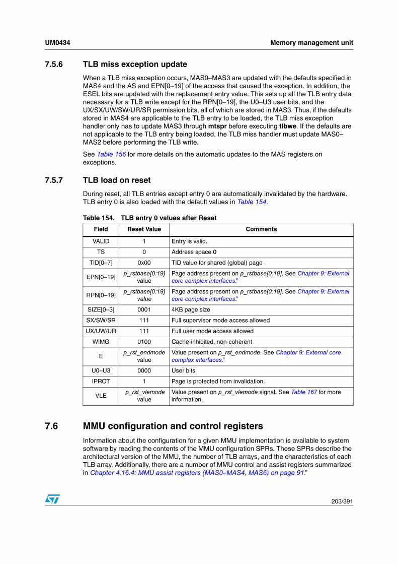
UM0434 Memory management unit
203/391
7.5.6 TLB miss exception update
When a TLB miss exception occurs, MAS0–MAS3 are updated with the defaults specified in MAS4 and the AS and EPN[0–19] of the access that caused the exception. In addition, the ESEL bits are updated with the replacement entry value. This sets up all the TLB entry data necessary for a TLB write except for the RPN[0–19], the U0–U3 user bits, and the UX/SX/UW/SW/UR/SR permission bits, all of which are stored in MAS3. Thus, if the defaults stored in MAS4 are applicable to the TLB entry to be loaded, the TLB miss exception handler only has to update MAS3 through mtspr before executing tlbwe. If the defaults are not applicable to the TLB entry being loaded, the TLB miss handler must update MAS0–MAS2 before performing the TLB write.
See Table 156 for more details on the automatic updates to the MAS registers on exceptions.
7.5.7 TLB load on reset
During reset, all TLB entries except entry 0 are automatically invalidated by the hardware. TLB entry 0 is also loaded with the default values in Table 154.
7.6 MMU configuration and control registersInformation about the configuration for a given MMU implementation is available to system software by reading the contents of the MMU configuration SPRs. These SPRs describe the architectural version of the MMU, the number of TLB arrays, and the characteristics of each TLB array. Additionally, there are a number of MMU control and assist registers summarized in Chapter 4.16.4: MMU assist registers (MAS0–MAS4, MAS6) on page 91.”
Table 154. TLB entry 0 values after Reset
Field Reset Value Comments
VALID 1 Entry is valid.
TS 0 Address space 0
TID[0–7] 0x00 TID value for shared (global) page
EPN[0–19]p_rstbase[0:19]
valuePage address present on p_rstbase[0:19]. See Chapter 9: External core complex interfaces.”
RPN[0–19]p_rstbase[0:19]
valuePage address present on p_rstbase[0:19]. See Chapter 9: External core complex interfaces.”
SIZE[0–3] 0001 4KB page size
SX/SW/SR 111 Full supervisor mode access allowed
UX/UW/UR 111 Full user mode access allowed
WIMG 0100 Cache-inhibited, non-coherent
Ep_rst_endmode
valueValue present on p_rst_endmode. See Chapter 9: External core complex interfaces.”
U0–U3 0000 User bits
IPROT 1 Page is protected from invalidation.
VLE p_rst_vlemode
valueValue present on p_rst_vlemode signal. See Table 167 for more information.

Memory management unit UM0434
204/391
7.6.1 MMU configuration register (MMUCFG)
MMUCFG provides configuration information for the MMU supplied with this version of the e200z3 CPU core. See Chapter 4.16.2: MMU configuration register (MMUCFG).”
7.6.2 TLB0 and TLB1 configuration registers
TLB0CFG and TLB1CFG provide configuration information for the MMU TLBs supplied with this version of the e200z3 CPU core. See Chapter 4.16.3: TLB configuration registers (TLBnCFG).”
7.6.3 Data exception address register (DEAR)
DEAR, described in Chapter : Data exception address register (DEAR),” is loaded with the effective address of the data access that results in an alignment, data TLB miss, or data storage interrupt.
7.6.4 MMU control and status register 0 (MMUCSR0)
MMUCSR0, shown in Chapter 4.16.1,”controls the state of the MMU.
7.6.5 MMU assist registers (MAS)
The e200z3 uses MAS0–MAS4 and MAS6 SPRs to facilitate reading, writing, and searching the TLBs. The e200z3 does not implement MAS5, because the tlbsx instruction only searches based on a single SPID value.
MAS registers are described in Chapter 4.16.4.”
MAS registers summary
The fields of the MAS registers are summarized in Table 155.
Table 155. MMU assist registers summary
32 33 34 3536
37
38
39
40
41
42
43
44
45
4647
48
49
50
51
52
53
54
55
56
57
58 59 60 61 62 63
MAS0
—TLBSE
L— ESEL — NV
MAS1
VALID
IPROT
— TID —TS
TSIZ —
MAS2
EPN — VLE W I M G E
MAS3
RPN —U0
U1
U2
U3
UX SXUW
SW
UR
SR
MAS4
— TBSEL
D— TIDSELD — TSIZED —
VLED
WD
IDMD
GD
ED
MAS6
— SPID —SAS

UM0434 Memory management unit
205/391
MAS register updates
Table 156 details the updates to each MAS register field for each update type.
7.7 Effect of hardware debug on MMU operationHardware debug facilities use normal CPU instructions to access register and memory contents during a debug session. If desired, the debug firmware may disable the translation process and may substitute default values for the access protection (UX, UR, UW, SX, SR, SW) bits and values obtained from the OnCE control register for page attribute (W,I,M,G,E) bits normally provided by a matching TLB entry. In addition, no address translation is performed; instead, a 1:1 mapping of effective-to-real addresses is performed. When disabled during the debug, no TLB miss or TLB access protection related DSI conditions occur. If there is a need for the debugger to use normal translation process, the MMU may be left enabled in the OnCE OCR, and normal translation (including the possibility of a TLB miss or DSI) remains in effect. See: Chapter : OnCE control register (OCR),” for details on controlling MMU operation during debug sessions.
Table 156. MMU assist register field updates
Bit/FieldMAS
AffectedITLB/DTLB Error tlbsx hit tlbsx miss tlbre tlbwe
ISI/DSI
TLBSEL 0 TLBSELD ‘01’ TLBSELD NC(1) NC NC
ESEL 0 NV Matched entry NV NC NC NC
NV 0 NC NC NC NC NC NC
VALID 1 1 1 0 V(array) NC NC
IPROT 1 0Matched IPROT
0 IPROT(array) NC NC
TID[0–7] 1TIDSELD
(PID0,TIDZ)TID(array) SPID TID(array) NC NC
TS 1 MSR(IS/DS) SAS SAS TS(array) NC NC
TSIZE[0–3] 1 TSIZED TSIZE(array) TSIZED TSIZE(array) NC NC
EPN[0–19] 2 I/D EPN EPN(array) tlbsx EPN EPN(array) NC NC
WIMGE 2 Default values WIMGE(array)Default values
WIMGE(array) NC NC
RPN[0–19] 3 Zeroed RPN(Array) Zeroed RPN(array) NC NC
ACCESS(PERMISS + U0–U3)
3 Zeroed Access(Array) Zeroed Access(array) NC NC
TLBSELD 4 NC NC NC NC NC NC
TIDSELD[0–1] 4 NC NC NC NC NC NC
TSIZED[0–3] 4 NC NC NC NC NC NC
Default WIMGE 4 NC NC NC NC NC NC
SPID 6 PID0 NC NC NC NC NC
SAS 6 MSR(IS/DS) NC NC NC NC NC
1. NC—no change

Instruction pipeline and execution timing UM0434
206/391
8 Instruction pipeline and execution timing
This chapter describes the instruction pipeline and instruction timing information. The core is partitioned into the following systems:
● Instruction unit
● Control unit
● Integer unit
● Load/store unit
● Core interface
8.1 Overview of operationFigure 12 shows a block diagram of the e200z3 core. The instruction fetch unit prefetches instructions from memory into the instruction buffers. The decode unit decodes each instruction and generates information needed by the branch and execution units. Branch target instructions are written into the branch target prefetch buffers; sequentially prefetched instructions are written into the instruction buffers.
The instruction fetch unit attempts to supply a constant stream of instructions to the execution pipeline. It does so by decoding and detecting branches early in the instruction buffer, making branch predictions, and prefetching their branch targets into the instruction buffer. By prefetching the branch targets early, some or all of the branch pipeline bubbles can be hidden from the execution pipeline.
The instruction issue unit attempts to issue a single instruction each cycle to one of the execution units. Source operands for each of the instructions are provided from the GPRs or from the operand feed-forward muxes. Data or resource hazards may create conditions that stall instruction issue until the hazard is eliminated.
The execution units write the result of a finished instruction onto the proper result bus and into the destination registers. The writeback logic retires an instruction when the instruction has finished execution. Up to two results can be simultaneously written.

UM0434 Instruction pipeline and execution timing
207/391
Figure 12. e200z3 block diagram
8.1.1 Control unit
The control unit coordinates the instruction fetch unit, branch unit, instruction decode unit, instruction issue unit, completion unit, and exception handling logic.
8.1.2 Instruction unit
The instruction unit controls the flow of instructions to the instruction buffers and decode unit. Six prefetch buffers allow the instruction unit to fetch instructions ahead of actual execution, and serve to decouple memory and the execution pipeline.
CPU
Load/
Data
Memory
Address
StoreUnit
Instruction Unit
BranchUnit
PCUnit
Instruction Buffer
GPRCRSPR
MultiplyUnit
Data Bus Interface Unit
Control
32 64 N
OnCE/Nexus
Interface
Control
Data
(mtspr/mfspr)
IntegerExecution
Unit
ExternalSPR
CTRXER
LR
Data
Address
Instruction Bus Interface U
nit
Control
32
64
N
Control Logic Control Logic
ManagementUnit

Instruction pipeline and execution timing UM0434
208/391
8.1.3 Branch unit
The branch unit contains an eight-entry branch target buffer (BTB) to accelerate execution of branch instructions.
Untaken conditional branches execute in a single clock. Branches with successful target prefetching have an effective execution time of one clock cycle. All other taken branches have an execution time of two clocks.
8.1.4 Instruction decode unit
The decode unit includes the instruction buffers. A single instruction can be decoded each cycle. The major functions of the decode logic are as follows:
● Opcode decoding to determine the instruction class and resource requirements for each instruction being decoded.
● Source and destination register dependency checking.
● Execution unit assignment.
● Determine any decode serializations and inhibit subsequent instruction decoding.
The decode unit operates in a single processor clock cycle.
8.1.5 Exception handling
The exception handling unit includes logic to handle exceptions, interrupts, and traps.
8.2 Execution unitsThe core data execution units consist of the integer unit and the load/store unit. Included in the execution units section are the general purpose registers (GPRs). Instructions with data dependencies begin execution when all such dependencies are resolved.
8.2.1 Integer execution unit
The integer execution unit is used to process arithmetic and logical instructions. Adds, subtracts, compares, count leading zeros, shifts, and rotates execute in a single cycle.
Multiply instructions have a latency and throughput rate of 1 cycle.
Divide instructions have a variable latency (6–16 cycles) depending on the operand data. The worst case integer divide requires 16 cycles. While the divide is running, the rest of the pipeline is unavailable for additional instructions (blocking divide).
8.2.2 Load/Store unit
The load/store unit executes instructions that move data between the GPRs and the memory subsystem. A load followed by a dependent instruction does not incur any pipeline stall, except when the dependent instruction is a load/store instruction, and the latter instruction is using the previous load data for its effective address (EA) calculation.
Loads, when free of the above EA calculation dependency, execute with a maximum throughput of one per cycle and one-cycle latency. Store data can be fed forward from an immediately preceding load with no stall.
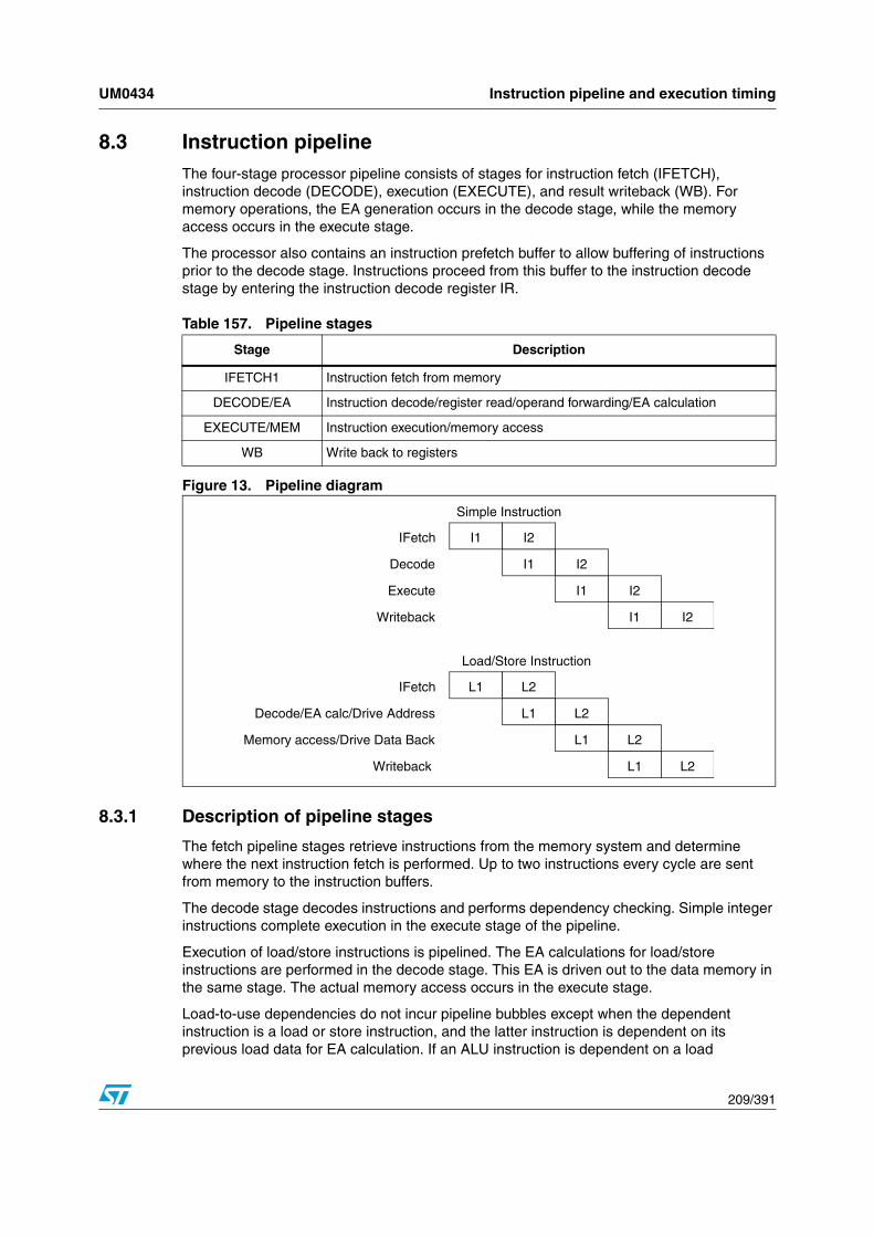
UM0434 Instruction pipeline and execution timing
209/391
8.3 Instruction pipelineThe four-stage processor pipeline consists of stages for instruction fetch (IFETCH), instruction decode (DECODE), execution (EXECUTE), and result writeback (WB). For memory operations, the EA generation occurs in the decode stage, while the memory access occurs in the execute stage.
The processor also contains an instruction prefetch buffer to allow buffering of instructions prior to the decode stage. Instructions proceed from this buffer to the instruction decode stage by entering the instruction decode register IR.
Figure 13. Pipeline diagram
8.3.1 Description of pipeline stages
The fetch pipeline stages retrieve instructions from the memory system and determine where the next instruction fetch is performed. Up to two instructions every cycle are sent from memory to the instruction buffers.
The decode stage decodes instructions and performs dependency checking. Simple integer instructions complete execution in the execute stage of the pipeline.
Execution of load/store instructions is pipelined. The EA calculations for load/store instructions are performed in the decode stage. This EA is driven out to the data memory in the same stage. The actual memory access occurs in the execute stage.
Load-to-use dependencies do not incur pipeline bubbles except when the dependent instruction is a load or store instruction, and the latter instruction is dependent on its previous load data for EA calculation. If an ALU instruction is dependent on a load
Table 157. Pipeline stages
Stage Description
IFETCH1 Instruction fetch from memory
DECODE/EA Instruction decode/register read/operand forwarding/EA calculation
EXECUTE/MEM Instruction execution/memory access
WB Write back to registers
IFetch
Decode
Execute
Writeback I1 I2
IFetch
Decode/EA calc/Drive Address
Memory access/Drive Data Back
L1 L2
L1 L2
L1 L2
Writeback L1 L2
Simple Instruction
Load/Store Instruction
I1 I2
I1 I2
I1 I2

Instruction pipeline and execution timing UM0434
210/391
instruction, the data is fed directly into the ALU for execution. No pipeline bubble is incurred in this case.
Multiply instructions require one clock to execute. All condition-setting instructions complete in the execute stage of the pipeline.
Feed-forwarding allows the result of one instruction to be made available as the source operand(s) of a subsequent instruction so that data-dependent instructions can execute without waiting for previous instructions to write back their results.
8.3.2 Instruction buffers
The e200z3 contains a set of instruction buffers that supply instructions into the instruction register (IR) for decoding.
Instruction prefetches request a 64-bit double word and the buffer is filled with a pair of instructions at a time, except for the case of a change of flow fetch where the target is to the second (odd) word. In that case, only a 32-bit prefetch is performed to load the instruction buffer. This 32-bit fetch may be immediately followed by a 64-bit prefetch to fill slots 0 and 1 in the event that the branch is resolved to be taken.
In normal sequential execution, instructions are loaded into the IR from slot 0, and as a pair of slots are emptied, they are refilled. Whenever a pair of slots is empty, a 64-bit prefetch is initiated that fills the earliest empty slot pairs beginning with slot 0.
If the instruction buffer empties, instruction issue stalls, and the buffer is refilled. The first returned instruction is forwarded directly to the IR.
Figure 14. Instruction buffers
Slot0
Decode
..
MUX
IR
DATA 0:63
Slot1
Slot2
Slot3

UM0434 Instruction pipeline and execution timing
211/391
HID0[BPRED] controls if prediction is made for forward or backward branches (or both).
To resolve branch instructions and improve the accuracy of branch predictions, the e200z3 implements a dynamic branch prediction mechanism using an 8-entry branch target buffer (BTB), a fully associative address cache of branch target addresses. The BTB is purposefully small to reduce cost and power. It is expected to accelerate the execution of loops with some potential change of flow within the loop body.
An entry is allocated in the BTB whenever a branch resolves as taken and the BTB is enabled. Branches that have not been allocated are always predicted as not taken. BTB entries are allocated on taken branches using a FIFO replacement algorithm.
Each BTB entry holds a 2-bit branch history counter, whose value is incremented or decremented on a BTB hit, depending on whether the branch was taken. The counter can assume four different values: strongly taken, weakly taken, weakly not taken, and strongly not taken.
A branch is predicted as taken on a hit in the BTB with a counter value of strongly or weakly taken. In this case, the target address contained in the BTB is used to redirect the instruction fetch stream to the target of the branch prior to the branch reaching the instruction decode stage. In the case of a mispredicted branch, the instruction fetch stream returns to the sequential instruction stream after the branch has been resolved.
When a branch is predicted taken and the branch is later resolved (in the branch decode stage), the value of the counter is updated. A branch whose counter indicates weakly taken is resolved as taken, the counter increments so that the prediction becomes strongly taken. If the branch resolves as not taken, the prediction changes to weakly not-taken. The counter saturates in the strongly taken states when the prediction is correct.
The e200z3 does not implement the static branch prediction that is defined by the PowerPC architecture. The BO prediction bit in branch encodings is ignored.
Dynamic branch prediction is enabled by setting BUCSR[BPEN]. Clearing BUCSR[BPEN] disables dynamic branch prediction, in which case the e200z3 predicts every branch as not taken. Additional control is available in the HID0[BPRED] field to control whether forward or backward branches (or both) are candidates for entry into the BTB, and thus for branch prediction. Once a branch is in the BTB, HID0[BPRED] has no further effect on that entry.
The BTB uses virtual addresses for performing tag comparisons. On allocation of a BTB entry, the EA of a taken branch, along with the current instruction space (as indicated by MSR[IS]) is loaded into the entry, and the counter value is set to weakly taken. The current PID value is not maintained as part of the tag information.
The BTB is automatically flushed when the current PID value is updated by an mtspr PID instruction. Software is otherwise responsible for maintaining coherency in the BTB when a change in effective-to-real (virtual-to-physical) address mapping is changed. This is supported by the BUCSR[BBFI] control bit.

Instruction pipeline and execution timing UM0434
212/391
Figure 15. Branch target buffer
8.3.3 Single-Cycle instruction pipeline operation
Sequences of single-cycle execution instructions follow the flow in Figure 16. Instructions are issued and completed in program order. Most arithmetic and logical instructions fall into this category.
Figure 16. Basic pipeline flow, Single-Cycle instructions
8.3.4 Basic load and store instruction pipeline operation
The EA calculations for load and store instructions are performed in the decode stage. The memory access occurs in the execution stage.
If a load instruction is followed by a dependent ALU instruction, the load data is driven from the memory in the MEM stage and feed-forwarded into the dependent ALU instruction in the following cycle. As a result, there is no load-to-use pipeline bubble. Figure 17 shows the instruction flow for a load instruction followed by a dependent add instruction.
Figure 17. A load followed by a dependent add instruction
Tag Data
IS Counter
Counter
Counter
3
IS = Instruction Space
... ...... ... 2
IS 1
Branch addr[0:29]
Branch addr[0:29]
Branch addr[0:29]
Target address[0:29]
Target address[0:29]
Target address[0:29]
IS Entry
Entry
Entry
Entry
0
IFETCH DECODE EXECUTEFirst Inst.
Time Slot
FFwd/WB
Second Instruction
Third Instruction
IFETCH DECODE EXECUTE FFwd/WB
IFETCH DECODE EXECUTE FFwd/WB
DEC/EA MEMFirst Load Instruction
Time Slot
MEM
Second Add Instruction DECODE EXECUTE MEM
IFETCH
IFETCH
Feedforward

UM0434 Instruction pipeline and execution timing
213/391
Back-to-back load/store instructions are executed in a pipelined fashion, provided that their EA calculations are not dependent on their previous load instructions. Figure 18 shows the basic pipeline flow for two back-to-back load instructions. In this case, the second load does not depend on its previous load data for its EA calculation. Notice that the memory access of the first load instruction overlaps in time with the EA calculation of the second load instruction.
Figure 18. Back-to-Back load instructions
When a load is followed by a load or a store instruction that depends on the first load data for EA calculation, a pipeline stall is incurred. Figure 19 shows the instruction flow for a load instruction followed by a dependent store instruction through EA calculation. The second store instruction in this case is dependent on the first load instruction for its EA calculation.
Figure 19. A load followed by a dependent store instruction
A store instruction that depends on its previous load for its stored data, does not stall the pipeline.
8.3.5 Change-of-Flow instruction pipeline operation
A branch instruction takes either one or 2 cycles to execute. Simple change of flow instructions require 2 cycles to refill the pipeline with the target instruction for taken branches and branch and link instructions with no prediction.
For branch-type instructions, in some situations, this 2-cycle timing may be reduced by performing the target fetch speculatively while the branch instruction is still being fetched into the instruction buffer. The branch target address is obtained from the BTB. The resulting branch timing reduces to a single clock when the target fetch is initiated early enough and the branch is taken. Figure 20 shows basic pipeline flow for branch instructions.
DEC / EA MEMFirst Load Instruction
Time Slot
WB
Second Load Instruction DEC / EA MEM WB
IFETCH
IFETCH
DECODE EXECUTEFirst Load Instruction
Time Slot
WB
Second Store Instruction DECODE EA Calc MEM
IFETCH
IFETCH WB
Feedforward

Instruction pipeline and execution timing UM0434
214/391
Figure 20. Basic pipeline flow, branch instructions
Figure 21 shows basic pipeline flow for branch speculation.
Figure 21. Basic pipeline flow, branch speculation
8.3.6 Basic Multi-Cycle instruction pipeline operation
The divide instructions and the load and store multiple instructions require multiple cycles in the execute stage.
Figure 22. Basic pipeline flow, Multi-Cycle instructions
Instructions must complete and write back results in order. A single cycle instruction that follows a multi-cycle instruction must wait for completion of the multi-cycle instruction prior to its writeback in order to meet the in-order requirement. Result feed-forward paths are provided so that execution may continue prior to result writeback.
8.3.7 Additional examples of instruction pipeline operation for load & store
Figure 23 shows an example of pipelining two non–data-dependent load or store instructions with a following data-dependent single-cycle instruction. While the first load or store begins accessing memory in the MEM stage, the next load or store can be calculating a new EA in the DEC/EA stage. The add in this example does not stall despite a data dependency on its preceding load instruction.
DECODE EXECBR Inst.
Time Slot
Target Instruction EXEC WB . . .
IFETCH Slot0
IFETCH DECODE
IFETCH DECODEBranch Instruction
Time Slot
Target Instruction
Slot0
DECODE EXEC
(Speculative Fetch)
BTB hit TFETCH Slot0
. . .EXEC
IFETCH DECODE WBLoad/Store Multiple Word/Divide Instruction
Time Slot
EXEC0 EXECn. . .

UM0434 Instruction pipeline and execution timing
215/391
Figure 23. Pipelined Load/Store instructions
For memory access instructions, wait states may occur. This causes a following memory access instruction to stall since the following memory access may not be initiated as shown in Figure 24. Here, the first ld/st instruction incurs a wait state on the bus interface, causing succeeding instructions to stall.
Figure 24. Pipelined Load/Store instructions with Wait-State
8.3.8 Move to/from SPR instruction pipeline operation
Most mtspr and mfspr instructions are treated like single-cycle instructions in the pipeline and do not cause stalls. Exceptions are for the MSR, the debug SPRs, the embedded floating-point APUs, and MMU SPRs, which do cause stalls. Figure 25 through Figure 25 show examples of mtspr and mfspr instruction timing.
Figure 25 applies to the debug SPRs and the EFPU’s EFSCR. These instructions do not begin execution until all previous instructions have finished their execute stage. If a multicycle instruction precedes an mfspr or mtspr instruction, the mfspr or mtspr instruction does not begin execution until the preceding multicycle instruction moves into the writeback stage as shown in Figure 25. In addition, execution of subsequent instructions stalls until the mfspr and mtspr instructions complete.
First Load/Store Instruction (No Wait)
Time Slot
Second Load/Store Instruction (No Wait)
Add Instruction
IFETCH WBDEC/EA
IFETCH MEM WB DEC/EA
WB IFETCH EXECUTEDEC
MEM
First Load/Store Instruction (With Wait)
Time Slot
Second Load/Store Instruction (No Wait)
Add Instruction
IFETCH Stall (wait)DEC/EA WB
IFETCH Stall MEM DEC / EA WB
EXECUTEIFETCH DEC Stall WB
MEM

Instruction pipeline and execution timing UM0434
216/391
Figure 25. mtspr, mfspr instruction Execution—(1)
Figure 26 applies to the mtmsr, wrtee, and wrteei instructions. Execution of subsequent instructions stalls until these instructions writeback.
Figure 26. mtmysr, wrtee, wrteei instruction execution
Access to MMU SPRs stalls until all outstanding bus accesses complete and the MMU is idle (p_[i,d]_cmbusy negated) to allow an access window where no translations or cache cycles are required. Figure 27 shows an example where an outstanding bus access delays mtspr/mfspr execution until the bus becomes idle. Processor access requests are held off during execution of an MMU SPR instruction. A subsequent access request may be generated in the WB cycle. This same protocol applies to MMU management instructions (such as tlbre, tlbwe, etc.) as well as to the DCRs.
Time Slot
mtspr, mfspr
DEC EXE1IFETCH WBPrevious Instruction (Multicycle)
DEC EXEIFETCH WB
DEC StallIFETCH EXE WBNext Instruction
EXEn. . .
. . .
. . .
Stall
Stall
Time Slot
mtmsr, wrtee, wrteei
DEC EXEIFETCHPrevious Instruction
DEC EXEIFETCH WB
DEC StallIFETCH EXE WBNext Instruction
WB

UM0434 Instruction pipeline and execution timing
217/391
Figure 27. DCR, MMU mtspr, mfspr, and MMU management instruction execution
8.4 Stalls caused by accessing SPRsAn mfspr instruction preceded by an mtspr instruction cannot be issued until the mtspr completes.
8.5 Instruction serializationThe core requires three types of serialization:
● Completion serialization. A completion-serialized instruction is held for execution until all prior instructions have completed. The instruction executes when it is next to complete in program order. Results from these instructions are not available for or forwarded to subsequent instructions until the instruction completes. The following instructions are completion-serialized:
– Instructions that access or modify system control or status registers—mcrxr, mtmsr, wrtee, wrteei, mtspr, mfspr (except to CTR/LR)
– Instructions that manage TLBs
– Instructions defined by the architecture as context or execution synchronizing: isync, msync, rfi, rfci, rfdi, and sc
● Dispatch (decode/issue) serialization. Some instructions are dispatch-serialized by the core. An instruction that is dispatch-serialized prevents the next instruction from decoding until all instructions up to and including the dispatch-serialized instruction
Time Slot
DEC EXE WBIFETCH ... ...Single-Cycle Instruction
DEC StallIFETCH Stall EXE WBNext Instruction
p_[i,d]_treq_b
p_[i,d]_tbusy[0]_b
p_[i,d]_ta_b
p_rd_spr,p_wr_spr
p_[i,d]_cmbusy
mtspr, mfspr DEC StallIFETCH Stall EXE WB

Instruction pipeline and execution timing UM0434
218/391
completes. The isync, mbar, msync, rfi, rfci, rfdi, and sc instructions are dispatch-serialized.
● Refetch serialization. Refetch-serialized instructions inhibit dispatching of subsequent instructions and force a pipeline refill to refetch subsequent instructions after completion. These include the following:
– The context synchronizing instruction isync
– The rfi, rfci, rfdi, and sc instructions.
8.6 Interrupt recognition and exception processingFigure 28 shows timing for interrupt recognition and exception processing overhead. This example shows best-case response timing when an interrupt is received and processed during execution of a sequence of single-cycle instructions.
Figure 28. Interrupt recognition and handler instruction execution
Time Slot
IFETCH EXE WBDEC
Single cycleInstructions
DEC/ --IFETCH --
p_extint_bfinal sample point
p_iack
IFETCH EXE WBDEC1st Instruction of handler
1 2 3 4 5 6 7 8 9 10
ec_excp_detected*
update_esr*
update_msr*
* - internal operations
oldpc_->srr0*
oldmsr_->srr1*
Abort

UM0434 Instruction pipeline and execution timing
219/391
Figure 29 below, shows timing for interrupt recognition and exception processing overhead. This example shows best-case response timing when an interrupt is received and processed during execution of a load or store instruction. The fetch for the handler is delayed until completion of the load or store, regardless of the number of wait-states.
Figure 29. Interrupt recog. & handler instruction exe-load/store in progress
Time Slot
DEC/EA wait waitMemLoad/StoreInstructions
IFETCH Abort --DEC --
p_extint_bFinal Sample Point
p_iack
IFETCH EXE WBDECFirst Instruction of handler
1 2 3 4 5 6 7 8 9 10
IFETCH Stall StallDEC/ Stall
ec_excp_detected*
oldpc_->srr0*
oldmsr_->srr1*
update_esr*
update_msr*
* Internal Operations
11
WB
Abort

Instruction pipeline and execution timing UM0434
220/391
Figure 30 below, shows timing for interrupt recognition and exception processing overhead. This example shows best-case response timing when an interrupt is received and processed during execution of a multicycle interruptible instruction.
Figure 30. Interrupt recog. & handler instruction exe-multi-cycle instruction abort
8.7 Instruction timingsTable shows instruction timing for various instruction classes. Pipelined instructions are shown with cycles of total latency and throughput. Divide instructions are not pipelined and block other instructions from executing during divide execution.
Load/store multiple instruction cycles are represented as a fixed number of cycles plus a variable number of cycles where ‘n’ is the number of words accessed by the instruction. Additionally, cycle times marked with an ampersand (&) require additional cycles due to serialization.
Time Slot
Next Instruction
IFETCH EXE AbortDEC -- --Multi-Cycle
Interruptible
IFETCH Abort --DEC --
1 2 3 4 5 6 7 8 9 10
p_extint_b
Final Sample Point
p_iack
IFETCH EXE WBDECFirst Instruction of handler
ec_excp_detected*
oldpc_->srr0*
oldmsr_->srr1*
update_esr*
update_msr*
* Internal Operations
Instruction

UM0434 Instruction pipeline and execution timing
221/391
Instruction class cycle counts
Class of instructions Latency Throughput Special notes
Integer: add, sub, shift, rotate, logical, cntlzw
1 1
Integer: compare 1 1
Branch 2/1 2/1Branches take between 1 and 2 cycles to execute.
Multiply 1 1
Divide 6–16 6–16 Data dependent timing
CR logical 1 1
Loads (non-multiple) 1 1
Load multiple1 + n/2 (max)
1 + n/2 (max)Timing depends on n and address alignment.
Stores (non-multiple) 1 1
Store multiple1 + n/2 (max)
1 + n/2 (max)Timing depends on n and address alignment.
mtmsr, wrtee, wrteei 2& 2
mcrf 1 1
mfspr, mtspr 2& 2& Applies to debug SPRs, optional unit SPRs
mfspr, mfmsr 1 1 Applies to internal, non-debug SPRs
mfcr, mtcr 1 1
rfi, rfci, rfdi 3 -
sc 3 -
tw, twi 3 - Trap taken timing

Instruction pipeline and execution timing UM0434
222/391
Table 158 shows detailed timing for each instruction mnemonic along with serialization requirements. As this table shows, the VLE instructions have the same latencies and serialization as their equivalents in the PowerPC architecture. Those instructions are listed by their root mnemonic.
Table 158. Instruction timing by mnemonic
Mnemonic Latency Serialization Comments
addc[o][.] 1 None
adde[o][.] 1 None
addi, e_addi[.], e_add16i, e_add2i., se_addi 1 None
addic[.], e_addic[.] 1 None
addis, e_add2is 1 None
addme[o][.] 1 None
addze[o][.] 1 None
add[o][.], se_add 1 None
andc[.], se_andc 1 None
andi., e_andi[.], e_and2i., se_andi 1 None
andis., e_and2is. 1 None
and[.], se_and[.] 1 None
bcctr[l] 2 None
bclr[l] 2 None
bc[l][a], e_bc, e_bcl, se_bc, se_bclri, se_bctr,se_bctrl
2/1 None
b[l][a], e_b, e_bl, se_b, se_bl, se_blr, se_blrl,se_bgeni
2/1 None
cmp, e_cmph, e_cmph16i, se_cmp 1 None
cmpi, e_cmphl, e_cmphl16i, se_cmph,se_cmphl
1 None
cmpl, e_cmpi, e_cmp16i, se_cmpi 1 None
cmpli, e_cmpli, e_cmpl16i, se_cmpl, se_cmpli 1 None
cntlzw[.] 1 None
crand, e_crand 1 None
crandc, e_crandc 1 None
creqv, e_creqv 1 None
crnand, e_crnand 1 None
crnor, e_crnor 1 None
cror, e_cror 1 None
crorc, e_crorc 1 None

UM0434 Instruction pipeline and execution timing
223/391
crxor, e_crxor 1 None
divwu[o][.] 6–16 None
divw[o][.] 6–16 None
With early-out capability timing is data dependent
eqv[.] 1 None
extsb[.], se_extsb 1 None
extsh[.], se_extsh 1 None
e_li, e_lis, se_li 1 None
The UISA defines li as a simplified, mnemonic for addi.
e_rlw, e_rlwi 1 None
isel 1 None
isync, se_isync3 Refetch
Plus additional synchronization time
lbz, e_lbz, se_lbz 1 None Aligned
lbzu, e_lbzu 1 None Aligned
lbzux, e_lha 1 None Aligned
lbzx, e_lhau 1 None Aligned
lha, e_lhz 1 None Aligned
lhau, e_lhzu 1 None Aligned
lhaux 1 None Aligned
lhax 1 None Aligned
lhbrx 1 None Aligned
lhz, se_lhz 1 None Aligned
lhzu 1 None Aligned
lhzux 1 None Aligned
lhzx 1 None Aligned
lmw, e_lmw 1 +(n/2) None
lwarx 1 None
lwbrx 1 None Aligned
lwz, e_lwz, se_lwz 1 None Aligned
lwzu, e_lwzu 1 None Aligned
Table 158. Instruction timing by mnemonic (continued)
Mnemonic Latency Serialization Comments

Instruction pipeline and execution timing UM0434
224/391
lwzux 1 None Aligned
lwzx 1 None Aligned
mbar1 Completion
Plus additional synchronization time
mcrf, e_mcrf 1 None
mcrxr 1 Completion
mfcr 1 None
mfmsr 1 None
mfspr (except, debug, MMU), se_mfctr, se_mflr 1 None
mfspr, (debug, MMU)3 Completion
Plus additional synchronization time
msync1 Completion
Plus additional synchronization time
mtcrf 2 None
mtmsr2 Completion
Plus additional synchronization time
mtspr, (debug, MMU), se_mtctr, se_mtlr2 Completion
Plus additional synchronization time
mtspr, (except, debug, MMU) 1 None
mulhwu[.] 1 None
mulhw[.] 1 None
mulli, e_mulli, e_mull2i 1 None
mullw[o][.], se_mullw 1 None
nand[.] 1 None
neg[o][.], se_neg 1 None
nop, (ori, r0r00) 1 None
nor[.], e_ori[.], e_or2i, e_or2is 1 None
orc[.] 1 None
ori 1 None
oris 1 None
or[.], se_or 1 None
rfci 3 Refetch
Table 158. Instruction timing by mnemonic (continued)
Mnemonic Latency Serialization Comments

UM0434 Instruction pipeline and execution timing
225/391
rfdi 3 Refetch
rfi 3 Refetch
rlwimi[.], e_rlwimi 1 None
rlwinm[.], e_rlwinm 1 None
rlwnm[.] 1 None
sc 3 Refetch
se_bmski 1 None
se_bseti 1 None
se_btsti 1 None
se_extzb, se_extzh 1 None
se_mfar 1 None
se_mr 1 None
The UISA defines mr as a simplified, mnemonic for or.
se_mtar 1 None
se_not 1 None
slw[.], se_slw, e_slwi, se_slwi 1 None
srawi[.], se_srawi 1 None
sraw[.], se_sraw 1 None
srw[.], se_srw, e_srwi, se_srwi 1 None
stb, e_stb, se_stb 1 None Aligned
stbu, e_stbu 1 None Aligned
stbux 1 None Aligned
stbx 1 None Aligned
sth, sth, e_sth, se_sth, e_sthu 1 None Aligned
sthbrx 1 None Aligned
sthu 1 None Aligned
sthux 1 None Aligned
sthx 1 None Aligned
stmw, e_stmw 1 + (n/2) None
stw, e_stw, se_stw 1 None Aligned
stwbrx 1 None Aligned
stwcx. 1 None
Table 158. Instruction timing by mnemonic (continued)
Mnemonic Latency Serialization Comments

Instruction pipeline and execution timing UM0434
226/391
8.7.1 SPE and embedded Floating-Point instruction timing
The tables in this section show instruction timing for SPE and embedded floating-point APU instructions. Pipelined instructions are shown with cycles of total latency and throughput cycles. Divide instructions are not pipelined and block other instructions from executing during divide execution.
Instruction pipelining is affected by the possibility of a floating-point instruction generating an exception. A load or store class instruction that follows an SPE FPU instruction stalls until it can be ensured that no previous instruction can generate a floating-point exception. This determination is based on which floating-point exception enable bits are set (FINVE, FOVFE, FUNFE, FDBZE, and FINXE) and at what point in the FPU pipeline an exception can be guaranteed to not occur. Invalid input operands are detected in the first stage of the pipeline, while underflow, overflow, and inexactness are determined later in the pipeline. Best overall performance occurs when either floating-point exceptions are disabled, or when load and store class instructions are scheduled such that previous floating-point instructions have already resolved the possibility of exceptional results.
SPE integer simple instructions timing
Instruction timing for SPE integer simple instructions is shown in Table 159. The table is sorted by opcode. These instructions are issued as a pair of operations.
stwu, e_stwu 1 None Aligned
stwux 1 None Aligned
stwx 1 None Aligned
subfc[o][.] 1 None
subfe[o][.] 1 None
subfic, e_subfic[.], se_subi[.] 1 None
subfme[o][.] 1 None
subfze[o][.] 1 None
subf[o][.], se_subf, se_sub 1 None
tw 3 None
twi 3 None
wrtee 2 Completion
wrteei 2 Completion
xori, e_xori[.] 1 None
xoris 1 None
xor[.] 1 None
Table 158. Instruction timing by mnemonic (continued)
Mnemonic Latency Serialization Comments

UM0434 Instruction pipeline and execution timing
227/391
Table 159. Timing for integer simple instructions
Instruction Latency Throughput Comments
brinc 1 1
evabs 1 1
evaddiw 1 1
evaddw 1 1
evand 1 1
evandc 1 1
evcmpeq 1 1
evcmpgts 1 1
evcmpgtu 1 1
evcmplts 1 1
evcmpltu 1 1
evcntlsw 1 1
evcntlzw 1 1
eveqv 1 1
evextsb 1 1
evextsh 1 1
evmergehi 1 1
evmergehilo 1 1
evmergelo 1 1
evmergelohi 1 1
evnand 1 1
evneg 1 1
evnor 1 1
evor 1 1
evorc 1 1
evrlw 1 1
evrlwi 1 1
evrndw 1 1
evsel 1 1
evslw 1 1
evslwi 1 1
evsplatfi 1 1
evsplati 1 1
evsrwis 1 1
evsrwiu 1 1

Instruction pipeline and execution timing UM0434
228/391
SPE load and store instruction timing
Instruction timing for SPE load and store instructions is shown in Table 160. The table is sorted by opcode. Actual timing depends on alignment; the table indicates timing for aligned operands.
evsrws 1 1
evsrwu 1 1
evsubfw 1 1
evsubifw 1 1
evxor 1 1
Table 160. SPE load and store instruction timing
Instruction Latency Throughput Comments
evldd 1 1
evlddx 1 1
evldh 1 1
evldhx 1 1
evldw 1 1
evldwx 1 1
evlhhesplat 1 1
evlhhesplatx 1 1
evlhhossplat 1 1
evlhhossplatx 1 1
evlhhousplat 1 1
evlhhousplatx 1 1
evlwhe 1 1
evlwhex 1 1
evlwhos 1 1
evlwhosx 1 1
evlwhou 1 1
evlwhoux 1 1
evlwhsplat 1 1
evlwhsplatx 1 1
evlwwsplat 1 1
evlwwsplatx 1 1
evstdd 1 1
Table 159. Timing for integer simple instructions (continued)
Instruction Latency Throughput Comments

UM0434 Instruction pipeline and execution timing
229/391
SPE complex integer instruction timing
Timings for SPE complex integer instructions are shown in Table 161. The table is sorted by opcode. For the divide instructions, the number of stall cycles is (latency) for following instructions.
evstddx 1 1
evstdh 1 1
evstdhx 1 1
evstdw 1 1
evstdwx 1 1
evstwhe 1 1
evstwhex 1 1
evstwho 1 1
evstwhox 1 1
evstwwe 1 1
evstwwex 1 1
evstwwo 1 1
evstwwox 1 1
Table 161. SPE complex integer instruction timing
Instruction Latency Throughput Comments
evaddsmiaaw 1 1
evaddssiaaw 1 1
evaddumiaaw 1 1
evaddusiaaw 1 1
evdivws 12–32 12–32 Timings are data dependent
evdivwu 12–32 12–32 Timings are data dependent
evmhegsmfaa 1 1
evmhegsmfan 1 1
evmhegsmiaa 1 1
evmhegsmian 1 1
evmhegumiaa 1 1
evmhegumian 1 1
evmhesmf 1 1
evmhesmfa 1 1
evmhesmfaaw 1 1
Table 160. SPE load and store instruction timing (continued)
Instruction Latency Throughput Comments

Instruction pipeline and execution timing UM0434
230/391
evmhesmfanw 1 1
evmhesmi 1 1
evmhesmia 1 1
evmhesmiaaw 1 1
evmhesmianw 1 1
evmhessf 1 1
evmhessfa 1 1
evmhessfaaw 1 1
evmhessfanw 1 1
evmhessiaaw 1 1
evmhessianw 1 1
evmheumi 1 1
evmheumia 1 1
evmheumiaaw 1 1
evmheumianw 1 1
evmheusiaaw 1 1
evmheusianw 1 1
evmhogsmfaa 1 1
evmhogsmfan 1 1
evmhogsmiaa 1 1
evmhogsmian 1 1
evmhogumiaa 1 1
evmhogumian 1 1
evmhosmf 1 1
evmhosmfa 1 1
evmhosmfaaw 1 1
evmhosmfanw 1 1
evmhosmi 1 1
evmhosmia 1 1
evmhosmiaaw 1 1
evmhosmianw 1 1
evmhossf 1 1
evmhossfa 1 1
evmhossfaaw 1 1
evmhossfanw 1 1
Table 161. SPE complex integer instruction timing (continued)
Instruction Latency Throughput Comments
UM0434 Instruction pipeline and execution timing
231/391
evmhossiaaw 1 1
evmhossianw 1 1
evmhoumi 1 1
evmhoumia 1 1
evmhoumiaaw 1 1
evmhoumianw 1 1
evmhousiaaw 1 1
evmhousianw 1 1
evmra 1 1
evmwhsmf 1 1
evmwhsmfa 1 1
evmwhsmi 1 1
evmwhsmia 1 1
evmwhssf 1 1
evmwhssfa 1 1
evmwhumi 1 1
evmwhumia 1 1
evmwlsmiaaw 1 1
evmwlsmianw 1 1
evmwlssiaaw 1 1
evmwlssianw 1 1
evmwlumi 1 1
evmwlumia 1 1
evmwlumiaaw 1 1
evmwlumianw 1 1
evmwlusiaaw 1 1
evmwlusianw 1 1
evmwsmf 1 1
evmwsmfa 1 1
evmwsmfaa 1 1
evmwsmfan 1 1
evmwsmi 1 1
evmwsmia 1 1
evmwsmiaa 1 1
evmwsmian 1 1
Table 161. SPE complex integer instruction timing (continued)
Instruction Latency Throughput Comments

Instruction pipeline and execution timing UM0434
232/391
Vector Floating-Point APU instruction timing
Timings for embedded vector single-precision floating-point instructions are shown in Table 159. The number of stall cycles for evfsdiv is (latency) cycles.
evmwssf 1 1
evmwssfa 1 1
evmwssfaa 1 1
evmwssfan 1 1
evmwumi 1 1
evmwumia 1 1
evmwumiaa 1 1
evmwumian 1 1
evsubfsmiaaw 1 1
evsubfssiaaw 1 1
evsubfumiaaw 1 1
evsubfusiaaw 1 1
Table 162. SPE vector Floating-Point instruction timing
Instruction Latency Throughput Comments
evfsabs 1 1
evfsadd 1 1
evfscfsf 1 1
evfscfsi 1 1
evfscfuf 1 1
evfscfui 1 1
evfscmpeq 1 1
evfscmpgt 1 1
evfscmplt 1 1
evfsctsf 1 1
evfsctsi 1 1
evfsctsiz 1 1
evfsctuf 1 1
evfsctui 1 1
evfsctuiz 1 1
evfsdiv 12 12 Blocking, no overlap with next instruction
evfsmadd 1 1 Destination also used as source
Table 161. SPE complex integer instruction timing (continued)
Instruction Latency Throughput Comments

UM0434 Instruction pipeline and execution timing
233/391
SPE scalar Floating-Point instruction timing
Timings for embedded scalar single-precision floating-point APU instructions are shown in Table 163. The table is sorted by opcode.
evfsmsub 1 1 Destination also used as source
evfsmul 1 1
evfsnabs 1 1
evfsneg 1 1
evfsnmadd 1 1 Destination also used as source
evfsnmsub 1 1 Destination also used as source
evfssub 1 1
evfststeq 1 1
evfststgt 1 1
evfststlt 1 1
Table 163. Scalar SPE Floating-Point instruction timing
Instruction Latency Throughput Comments
efsabs 1 1
efsadd 1 1
efscfsf 1 1
efscfsi 1 1
efscfuf 1 1
efscfui 1 1
efscmpeq 1 1
efscmpgt 1 1
efscmplt 1 1
efsctsf 1 1
efsctsi 1 1
efsctsiz 1 1
efsctuf 1 1
efsctui 1 1
efsctuiz 1 1
efsdiv 12 12 Blocking, no execution overlap with next instruction
efsdiv 12 12 Blocking, no execution overlap with next instruction
efsmadd 1 1 Destination also used as source
efsmsub 1 1 Destination also used as source
Table 162. SPE vector Floating-Point instruction timing (continued)
Instruction Latency Throughput Comments
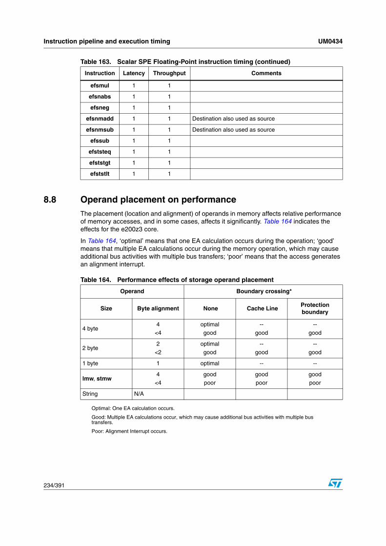
Instruction pipeline and execution timing UM0434
234/391
8.8 Operand placement on performanceThe placement (location and alignment) of operands in memory affects relative performance of memory accesses, and in some cases, affects it significantly. Table 164 indicates the effects for the e200z3 core.
In Table 164, ‘optimal’ means that one EA calculation occurs during the operation; ‘good’ means that multiple EA calculations occur during the memory operation, which may cause additional bus activities with multiple bus transfers; ‘poor’ means that the access generates an alignment interrupt.
efsmul 1 1
efsnabs 1 1
efsneg 1 1
efsnmadd 1 1 Destination also used as source
efsnmsub 1 1 Destination also used as source
efssub 1 1
efststeq 1 1
efststgt 1 1
efststlt 1 1
Table 163. Scalar SPE Floating-Point instruction timing (continued)
Instruction Latency Throughput Comments
Table 164. Performance effects of storage operand placement
Operand Boundary crossing*
Size Byte alignment None Cache LineProtection boundary
4 byte4
<4
optimal
good
--
good
--
good
2 byte2
<2
optimal
good
--
good
--
good
1 byte 1 optimal -- --
lmw, stmw4
<4
good
poor
good
poor
good
poor
String N/A
Optimal: One EA calculation occurs.
Good: Multiple EA calculations occur, which may cause additional bus activities with multiple bus transfers.
Poor: Alignment Interrupt occurs.

UM0434 External core complex interfaces
235/391
9 External core complex interfaces
This chapter describes the external interfaces of the e200z3 core complex. Signal descriptions as well as data transfer protocols are documented in the following subsections.
Chapter 9.4: Internal signals on page 265,” describes a number of internal signals that are not directly accessible to users, but they are mentioned in various chapters in this manual and aid in understanding the behavior of the core.
9.1 OverviewThe external interfaces encompass the following:
● Control and data signals supporting instruction and data transfers
● Support for interrupts, including vectored interrupt logic
● Reset support
● Power management interface signals
● Debug event signals
● Time base control and status information
● Processor state information
● Nexus 1/3/OnCE/JTAG interface signals
● A test interface
The memory interface that the BIU supports is based on the AMBA AHB-Lite subset of the AMBA 2.0 AHB, with V6 AMBA extensions. (Ref. documents ARM IHI 0011A, ARM DVI 0044A, and ARM PR022-GENC-001011 0.4). Sideband signals, described in this chapter, support additional control functions. A 64-bit data bus is implemented. The pipelined memory interface supports read and write transfers of 8, 16, 24, 32, and 64 bits, misaligned transfers, burst transfers of four double words, and true big- and little-endian operation.
Note: The AMBA AHB bit and byte ordering reflect a natural little-endian ordering that AMBA documentation uses. The BIU automatically performs byte lane conversions to support big-endian transfers. Memories and peripheral devices/interfaces should be wired according to byte lane addresses defined in Table 170.
Single-beat and misaligned transfers are supported for cache-inhibited read and write cycles, and write-buffer writes. Burst transfers (double-word–aligned) of 4 double words are supported for cache line-fill and copyback operations.
Misaligned accesses are supported with one or more transfers to the core interface. If an access is misaligned but lies within an aligned 64-bit double word, the core performs a single transfer. The memory interface delivers (reads) or accepts (writes) the data that corresponds to the size- and byte-enable signals aligned according to the 3 low-order address bits. If an access is misaligned and crosses a 64-bit boundary, the BIU performs a pair of transfers beginning at the effective address, requesting the original data size (either half word or word) for the first transfer, along with appropriate byte enables. For the second transfer, the address is incremented to the next 64-bit boundary, and the size and byte enable signals are driven to correspond to the number of remaining bytes to be transferred.

External core complex interfaces UM0434
236/391
9.2 Signal indexThis section contains an index of the core signals.
The following prefixes are used for signal mnemonics:
● 'm_' denotes master clock and reset signals.
● 'p_' denotes processor or core-related signals.
● 'j_' denotes JTAG mode signals.
● 'jd_' denotes JTAG and debug mode signals.
● 'ipt_' denotes scan and test mode signals.
● 'nex_' denotes Nexus3 signals.
Note: The “_b” suffix denotes active low signal. Signals with no active-low suffix are active high.
Figure 31 groups core bus and control signals by function.

UM0434 External core complex interfaces
237/391
Figure 31. Core signal groups
Transfer
Transfer
Transfer Control
Attributes
p_htrans[1:0]p_[d,i]_hburst[2:0]p_[d,i]_hbstrb[7:0]
Data Bus
p_doze, p_nap, p_sleep
p_reset_b
Reset-
Power
Address Busp_wakeup
p_haddr[31:0]
Management
* T These signals are internal to the core.
Note:
e200z3CPU
p_pstat[0:6], p_brstat[0:1]Processor Status
p_devt2p_devt1p_ude
p_halt, p_stop
p_halted, p_stopped
p_[d,i]_hwritep_[d,i]_hprot[5:0]p_[d,i]_hsize[1:0]p_[d,i]_hunalign
ReservationSignals
p_rsrvp_rsrv_clr
p_tbintp_tbclkTime Basep_tbdisable
Signals
DebugSupport
e200z3
Module
jd_debug_b
dbg_dbgrq*
cpu_dbgack *
OnCE Control *
JTAG Interface
jd_de_b
Test Interface
jd_de_en
jd_en_once
jd_watchot[0:n]
jd_mclk_on
j_en_once_regsel
m_porp_resetout_bp_rstbase[0:19]related
Signals
(OnCE/Debug)
p_d_hwdata[63:0]p_[d,i]_hrdata[63:0]
p_cpuid[0:7]Miscellaneous p_sysvers[0:31]
p_pvrin[16:31]SignalsProcessor
p_[d,i]_hresp[2:0]p_[d,i]hready
StatusTermination/
p_mcp_b
p_chkstopMachine Check
Interrupt
p_extint_bp_critint_bp_avec_bp_voffset[0:15]p_iack k
Signals
p_ipend
DevSupport
e200z3
Modulenex_mseo_b[1:0]
nex_evti_b
nex_mdo[n:0]
nex_mcko
nex_rdy_b
nex_evto_b
Clockm_clk
p_rst_endmode
p_[d,i]_hmaster[3:0]
MasterID nex_masterid[3:0]p_masterid[3:0]
Config
p_mcp_out
Nexus3
Nexus1
p_rst_vlemode

External core complex interfaces UM0434
238/391
Table 165 below, shows the core signal function and type, signal definition, and reset value. Signals are presented in functional groups.
Table 165. Interface signal definitions
Signal name I/O Reset Definition
Clock and signals related to reset
m_clk I Global system clock
m_por I Power-on reset
p_reset_b I Processor reset input
p_resetout_b O Processor reset output
p_rstbase[0:19] IReset exception handler base address, value to be loaded into TLB entry 0 on reset.
p_rst_endmode IReset endian mode select, value to be loaded into TLB entry 0 on reset.
p_rst_vlemode IReset VLE mode select, value to be loaded into TLB entry 0 on reset.
Memory interface signals
p_i_hmaster[3:0], p_d_hmaster[3:0]
O — Master ID
p_i_haddr[31:0], p_d_haddr[31:0] O — Address bus
p_i_hwrite, p_d_hwrite O 0 Write signal (always driven low for p_i_hwrite)
p_i_hprot[5:0], p_d_hprot[5:0] O — Protection codes
p_i_htrans[1:0], p_d_htrans[1:0] O — Transfer type
p_i_hburst[2:0] , p_d_hburst[2:0] O — Burst type
p_i_hsize[1:0], p_d_hsize[1:0] O — Transfer size
p_i_hunalign, p_d_hunalign O — Indicates that the current data access is misaligned
p_i_hbstrb[7:0] , p_d_hbstrb[7:0] O 0 Byte strobes
p_i_hrdata[63:0], p_d_hrdata[63:0] I Read data bus
p_d_hwdata[63:0] O — Write data bus
p_i_hready, p_d_hready I Transfer ready
p_i_hresp[2:0], p_d_hresp[2:0] I Transfer response
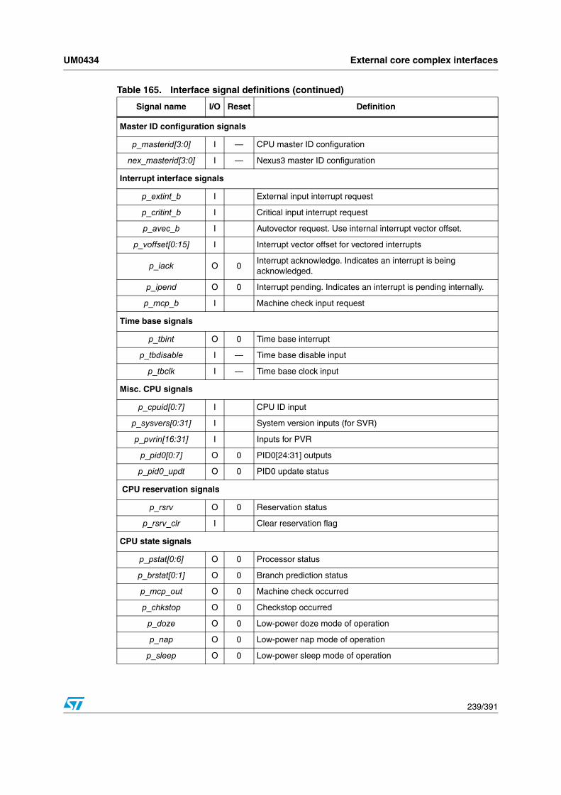
UM0434 External core complex interfaces
239/391
Master ID configuration signals
p_masterid[3:0] I — CPU master ID configuration
nex_masterid[3:0] I — Nexus3 master ID configuration
Interrupt interface signals
p_extint_b I External input interrupt request
p_critint_b I Critical input interrupt request
p_avec_b I Autovector request. Use internal interrupt vector offset.
p_voffset[0:15] I Interrupt vector offset for vectored interrupts
p_iack O 0Interrupt acknowledge. Indicates an interrupt is being acknowledged.
p_ipend O 0 Interrupt pending. Indicates an interrupt is pending internally.
p_mcp_b I Machine check input request
Time base signals
p_tbint O 0 Time base interrupt
p_tbdisable I — Time base disable input
p_tbclk I — Time base clock input
Misc. CPU signals
p_cpuid[0:7] I CPU ID input
p_sysvers[0:31] I System version inputs (for SVR)
p_pvrin[16:31] I Inputs for PVR
p_pid0[0:7] O 0 PID0[24:31] outputs
p_pid0_updt O 0 PID0 update status
CPU reservation signals
p_rsrv O 0 Reservation status
p_rsrv_clr I Clear reservation flag
CPU state signals
p_pstat[0:6] O 0 Processor status
p_brstat[0:1] O 0 Branch prediction status
p_mcp_out O 0 Machine check occurred
p_chkstop O 0 Checkstop occurred
p_doze O 0 Low-power doze mode of operation
p_nap O 0 Low-power nap mode of operation
p_sleep O 0 Low-power sleep mode of operation
Table 165. Interface signal definitions (continued)
Signal name I/O Reset Definition

External core complex interfaces UM0434
240/391
p_wakeup O 0Indicates to external clock control module to enable clocks and exit from low-power mode
p_halt I CPU halt request
p_halted O 0 CPU halted
p_stop I CPU stop request
p_stopped O 0 CPU stopped
CPU debug event signals
p_ude I Unconditional debug event
p_devt1 I Debug event 1 input
p_devt2 I Debug event 2 input
Debug/Emulation support signals (Nexus 1/OnCE)
jd_en_once I Enable full OnCE operation
jd_debug_b O 1 Processor entered debug session
jd_de_b I Debug request
jd_de_en O 0 Active-high output enable for DE_b open-drain IO cell
jd_mclk_on I System clock controller actively toggling m_clk
jd_watchpt[0:7] O 0 Address watchpoint occurred
Development support signals (Nexus 3)
nex_mcko O Nexus3 clock output
nex_rdy_b O Nexus3 ready output
nex_evto_b O Nexus3 event-out output
nex_evti_b I Nexus3 event-in input
nex_mdo[n:0] O Nexus3 message data output
nex_mseo_b[1:0] O Nexus3 message start/end output
JTAG-Related signals
j_trst_b I JTAG test reset from pad
j_tclk I JTAG test clock from pad
j_tms I JTAG test mode select from pad
j_tdi I JTAG test data input from pad
j_tdo O 0 JTAG test data out to master controller or pad
j_tdo_en O 0 Enables TDO output buffer
j_tst_log_rst O 0 Test-logic-reset state of JTAG controller
j_capture_ir O 0 Capture_IR state of JTAG controller
j_update_ir O 0 Update_IR state of JTAG controller
Table 165. Interface signal definitions (continued)
Signal name I/O Reset Definition

UM0434 External core complex interfaces
241/391
9.3 Signal descriptionsTable 166 describes the processor clock, m_clk.
Table 167 describes signals that are related to reset. The core supports several reset input signals for the CPU and JTAG/OnCE control logic: m_por, p_reset_b, and j_trst_b. The reset domains are partitioned such that the CPU p_reset_b signal does not affect JTAG/OnCE logic and j_trst_b does not affect processor logic. It is possible and desirable to access OnCE registers while the processor is running or in reset. It is also possible and desirable to assert j_trst_b and clear the JTAG/OnCE logic without affecting the processor state.
The synchronization logic between the processor and debug module requires an assertion of either j_trst_b or m_por during initial processor power-on reset to ensure proper operation. If the pin associated with j_trst_b is designed with a pull-up resistor and left floating, assertion of m_por is required during the initial power-on processor reset. Similarly, for those systems that do not have a power-on reset circuit and choose to tie m_por low, it is required to assert j_trst_b during processor power-up reset. When a power-up reset is achieved, the two resets can be asserted independently.
A reset output signal, p_resetout_b, is also provided.
j_shift_ir O 0 Shift_IR state of JTAG controller
j_capture_dr O 0 Parallel test data register load state of JTAG controller
j_shift_dr O 0 TAP controller in shift DR state
j_update_gp_reg O 0 Updates JTAG controller test data register
j_rti O 0 JTAG controller run-test-idle state
j_key_in IInput for providing data to be shifted out during shift_IR state when jd_en_once is negated
j_en_once_regsel O 0 External enable OnCE register select
j_nexus_regsel O 0 External Nexus register select
j_lsrl_regsel O 0 External LSRL register select
j_gp_regsel[0:11] O 0 General-purpose external JTAG register select
j_id_sequence[0:1] I JTAG ID register (2 msbs of sequence field)
j_id_version[0:3] I JTAG ID register version field
j_serial_data I Serial data from external JTAG registers
Table 165. Interface signal definitions (continued)
Signal name I/O Reset Definition
Table 166. Processor clock signal description
Signal I/O Signal description
m_clk IProcessor clock. The synchronous clock source for the core. Because the core is designed for static operation, m_clk can be gated off to lower power dissipation (for example, during low-power stopped states).
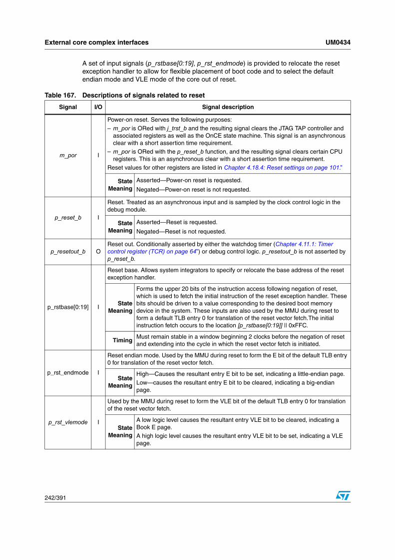
External core complex interfaces UM0434
242/391
A set of input signals (p_rstbase[0:19], p_rst_endmode) is provided to relocate the reset exception handler to allow for flexible placement of boot code and to select the default endian mode and VLE mode of the core out of reset.
Table 167. Descriptions of signals related to reset
Signal I/O Signal description
m_por I
Power-on reset. Serves the following purposes:
– m_por is ORed with j_trst_b and the resulting signal clears the JTAG TAP controller and associated registers as well as the OnCE state machine. This signal is an asynchronous clear with a short assertion time requirement.
– m_por is ORed with the p_reset_b function, and the resulting signal clears certain CPU registers. This is an asynchronous clear with a short assertion time requirement.
Reset values for other registers are listed in Chapter 4.18.4: Reset settings on page 101.”
StateMeaning
Asserted—Power-on reset is requested.
Negated—Power-on reset is not requested.
p_reset_b I
Reset. Treated as an asynchronous input and is sampled by the clock control logic in the debug module.
StateMeaning
Asserted—Reset is requested.
Negated—Reset is not requested.
p_resetout_b OReset out. Conditionally asserted by either the watchdog timer (Chapter 4.11.1: Timer control register (TCR) on page 64”) or debug control logic. p_resetout_b is not asserted by p_reset_b.
p_rstbase[0:19] I
Reset base. Allows system integrators to specify or relocate the base address of the reset exception handler.
StateMeaning
Forms the upper 20 bits of the instruction access following negation of reset, which is used to fetch the initial instruction of the reset exception handler. These bits should be driven to a value corresponding to the desired boot memory device in the system. These inputs are also used by the MMU during reset to form a default TLB entry 0 for translation of the reset vector fetch.The initial instruction fetch occurs to the location [p_rstbase[0:19]] || 0xFFC.
TimingMust remain stable in a window beginning 2 clocks before the negation of reset and extending into the cycle in which the reset vector fetch is initiated.
p_rst_endmode I
Reset endian mode. Used by the MMU during reset to form the E bit of the default TLB entry 0 for translation of the reset vector fetch.
StateMeaning
High—Causes the resultant entry E bit to be set, indicating a little-endian page.
Low—causes the resultant entry E bit to be cleared, indicating a big-endian page.
p_rst_vlemode I
Used by the MMU during reset to form the VLE bit of the default TLB entry 0 for translation of the reset vector fetch.
StateMeaning
A low logic level causes the resultant entry VLE bit to be cleared, indicating a Book E page. A high logic level causes the resultant entry VLE bit to be set, indicating a VLE page.

UM0434 External core complex interfaces
243/391
Table 168 describes signals for the address and data buses. These outputs provide the address for a bus transfer. According to the AHB definition, p_haddr31 is the msb and p_haddr0 is the lsb.
j_trst_b I
JTAG/OnCE reset (IEEE 1149.1 JTAG specification TRST).
StateMeaning
Asynchronous reset with a short assertion time requirement. It is ORed with the m_por function, and the resulting signal clears the OnCE TAP controller and associated registers and the OnCE state machine.
Table 167. Descriptions of signals related to reset (continued)
Signal I/O Signal description
Table 168. Descriptions of signals for the address and data buses
Signal I/O Signal description
p_[d,i]_haddr[31:0] OAddress bus. Provides the address for a bus transfer. According to the AHB definition, p_[d,i]_haddr[31] is the msb and p_[d,i]_haddr[0] is the lsb.
p_[d,i]_hrdata[63:0] I
Read data bus. Provides data to the core on read transfers. The read data bus can transfer 8, 16, 24, 32, or 64 bits per transfer. According to the AHB definition, p_[d,i]_hrdata63 is the msb and p_[d,i]_hrdata0 is the lsb.
Memory Byte AddressWired to p_[d,i]_hrdata Bits
0007:0
00115:8
01023:16
01131:24
10039:32
10147:40
11055:48
11163:56
p_d_hwdata[63:0] O
Write data bus. Transfers data from the core on write transfers. The write data bus can transfer 8, 16, 24, 32, or 64 bits of data per bus transfer. According to the AHB definition, p_d_hwdata[63] is the msb and p_d_hwdata[0] is the lsb.
Memory Byte AddressWired to p_d_hwdata Bits
0007:0
00115:8
01023:16
01131:24
10039:32
10147:40
11055:48
11163:56

External core complex interfaces UM0434
244/391
Table 169 describes transfer attribute signals, which provide additional information about the bus transfer cycle. Attributes are driven with the address at the start of a transfer.
Table 169. Descriptions of transfer attribute signals
Signal I/O Signal description
p_[d,i]_htrans[1:0] O
Transfer type. The processor drives p_[d,i]_htrans[1:0] to indicate the current transfer type as follows:00 DLE—No data transfer is required. Slaves must terminate IDLE transfers with a zero wait-state OKAY response and ignore the (non-existent) transfer.01 BUSY—(The core does not use the BUSY encoding and does not present this type of transfer to a bus slave.) Master is busy; burst transfer continues.10 NONSEQ—Indicates the first transfer of a burst, or a single transfer. Address and control signals are unrelated to the previous transfer.11 SEQ—Indicates the continuation of a burst. Address and control signals are related to the previous transfer. Control signals are the same. Address was incremented by the size of the data transferred (optionally wrapped).
If the p_[d,i]_htrans[1:0] encoding is not IDLE or BUSY, a transfer is being requested.
p_[d,i]_hwrite O
Write. Defines the data transfer direction for the current bus cycle.
StateMeaning
Asserted—The current bus cycle is a write.
Negated—The current bus cycle is a read.
p_[d,i]_hsize[1:0] O
Transfer size. For misaligned transfers, size may exceed the requested size to ensure that all asserted byte strobes are within the container defined by p_[d,i]_hsize[1:0]. Table 171 and Table 172 show p_[d,i]_hsize encodings for aligned and misaligned transfers.
00 Byte
01 Half word (2 bytes)10 Word (4 bytes)
11 Double word (8 bytes)

UM0434 External core complex interfaces
245/391
p_[d,i]_hburst[2:0]] O
Burst type. The core uses only SINGLE and WRAP4 burst types.
000 SINGLE—No burst, single beat only
001 INCR—Incrementing burst of unspecified length. Not used by the core.
p_[d,i]_hprot[5:0] O
Protection control. The core drives the p_[d,i]_hprot[5:0] signals to indicate the type of access for the current bus cycle. p_[d,i]_hprot[0] indicates instruction/data, p_[d,i]_hprot[1] indicates user/supervisor. p_[d,i]_hprot[5] indicates whether the access is exclusive (that is, for an lwarx or stwcx.). p_[d,i]_hprot[4:2] (allocate, cacheable, bufferable) indicate particular cache attributes for the access. The following table shows the definitions of the p_[d,i]_hprot[5:0] signals.
p_hprot5 p_hprot4 p_hprot3 p_hprot2 p_hprot1 p_hprot0 Transfer Type— — — — — 0 Instruction access— — — — — 1 Data access— — — — 0 — User mode access— — — — 1 — Supervisor mode
access— 0 0 0 — — Cache-inhibited— 0 0 1 — — Guarded, not
cache-inhibited— 0 1 0 — — Reserved— 0 1 1 — — Reserved— 1 0 0 — — Reserved— 1 0 1 — — Reserved— 1 1 0 — — Cacheable,
writethrough— 1 1 1 — — Cacheable,
writeback0 — — — — — Not exclusive1 — — — — — Exclusive access
The core maps Book E storage attributes to the AHB hprot signals as described in the following. For buffered stores, p_[d,i]_hprot[1] is driven with the user/supervisor mode attribute associated with the store at the time it was buffered. For cache line pushes/copybacks, p_[d,i]_hprot[1] indicates supervisor access. In both of these cases, p_[d,i]_hprot0 indicates a data access.
TLB[I] TLB[G] TLB[W]||!L1CSR0[CWM] p_hprot[4:2] Transfer Type0 0 0 111 Cacheable, writeback0 0 1 110 Cacheable, writethrough0 1 — 001 Guarded, not cache-inhibited1 — — 000 Cache-inhibited— — — 001 Buffered store, page marked
guarded— — — 110 Buffered store and page
marked writethrough or L1CSR0[CWM]=0, and non-guarded
— — — 111 Buffered store and page marked copyback and L1CSR0[CWM]=1, and non-guarded
— — — 111 Dirty line push
Table 169. Descriptions of transfer attribute signals (continued)
Signal I/O Signal description

External core complex interfaces UM0434
246/391
Table 170 describes signals for byte lane specification. Read transactions transfer from 1–8 bytes of data on the p_[d,i]_hrdata[63:0] bus. The lanes involved in the transfer are determined by the starting byte number specified by the lower address bits with the transfer size and byte strobes. Byte lane addressing is shown big-endian (left to right) regardless of the core’s endian mode. The byte in memory corresponding to address 0 is connected to B0 (p_h{r,w}data[7:0]) and the byte corresponding to address 7 is connected to B7 (p_h{r,w}data[63:56]). The CPU internally permutes read data as required for the endian mode of the current access. Assertion of p_[d,i]_hunalign indicates misaligned transfers and that byte strobes do not correspond exactly to size and low-order address bits.
Table 171 lists all data transfer permutations. Note that misaligned data requests that cross a 64-bit boundary are broken into two bus transactions, and the address value and size encoding for the first transfer are not modified. The table is arranged in a big-endian fashion, but the active lanes are the same regardless of the endian-mode of the access. The core performs the proper byte routing internally based on endianness.
Table 170. Descriptions of signals for byte lane specification
Signal I/O Signal description
p_[d,i]_hunalign O
Unaligned access. Indicates whether the current access is misaligned.
StateMeaning
Asserted—Asserted for misaligned data accesses and for misaligned instruction accesses from VLE pages. Normal Book E instruction pages are always aligned. When p_[d,i]_hunalign is asserted, the p_[d,i]_hbstrb[7:0] byte strobe signals indicate the selected bytes involved in the current portion of the misaligned access, which may not include all bytes defined by the size and low-order address signals. Aligned transfers also assert the byte strobes, but in a manner corresponding to size and low-order address bits.
Negated—No misaligned data access is occurring.
Timing The timing of this signal is approximately the same as address timing.
p_[d,i]_hbstrb[7:0] O
Byte strobes. Indicate the bytes selected for the current transfer. For a misaligned access, the current transfer may not include all bytes defined by the size and low-order address signals. For aligned transfers, the byte strobe signals correspond to the bytes that size and low-order address signals define. The relationships of byte addresses to the byte strobe signals are as follows.Memory byte address Wired to p_h{r,w}data bits Corresponding byte strobe signal
000 7:0 p_[d,i]_hbstrb[0]001 15:8 p_[d,i]_hbstrb[1]010 23:16 p_[d,i]_hbstrb[2]011 31:24 p_[d,i]_hbstrb[3]100 39:32 p_[d,i]_hbstrb[4]101 47:40 p_[d,i]_hbstrb[5]110 55:48 p_[d,i]_hbstrb[6]111 63:56 p_[d,i]_hbstrb[7]
Table 171. Byte strobe assertion for transfers
Program size and byte offset
A(2:0)HSIZE
[1:0]
Data bus byte strobesHUNALIGN
B0 B1 B2 B3 B4 B5 B6 B7
Byte @000 0 0 0 0 0 X — — — — — — — 0
Byte @001 0 0 1 0 0 — X — — — — — — 0
Byte @010 0 1 0 0 0 — — X — — — — — 0
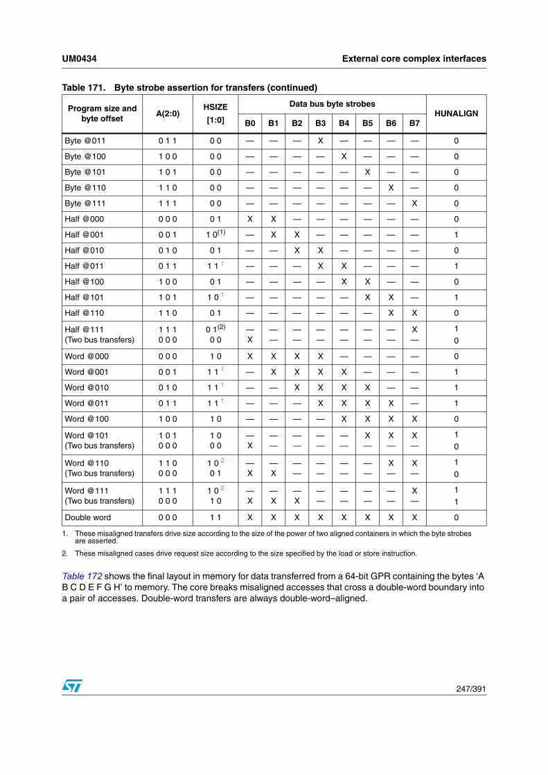
UM0434 External core complex interfaces
247/391
Table 172 shows the final layout in memory for data transferred from a 64-bit GPR containing the bytes ‘A B C D E F G H’ to memory. The core breaks misaligned accesses that cross a double-word boundary into a pair of accesses. Double-word transfers are always double-word–aligned.
Byte @011 0 1 1 0 0 — — — X — — — — 0
Byte @100 1 0 0 0 0 — — — — X — — — 0
Byte @101 1 0 1 0 0 — — — — — X — — 0
Byte @110 1 1 0 0 0 — — — — — — X — 0
Byte @111 1 1 1 0 0 — — — — — — — X 0
Half @000 0 0 0 0 1 X X — — — — — — 0
Half @001 0 0 1 1 0(1) — X X — — — — — 1
Half @010 0 1 0 0 1 — — X X — — — — 0
Half @011 0 1 1 1 1 1 — — — X X — — — 1
Half @100 1 0 0 0 1 — — — — X X — — 0
Half @101 1 0 1 1 0 1 — — — — — X X — 1
Half @110 1 1 0 0 1 — — — — — — X X 0
Half @111(Two bus transfers)
1 1 10 0 0
0 1(2)
0 0—X
——
——
——
——
——
——
X—
10
Word @000 0 0 0 1 0 X X X X — — — — 0
Word @001 0 0 1 1 1 1 — X X X X — — — 1
Word @010 0 1 0 1 1 1 — — X X X X — — 1
Word @011 0 1 1 1 1 1 — — — X X X X — 1
Word @100 1 0 0 1 0 — — — — X X X X 0
Word @101(Two bus transfers)
1 0 10 0 0
1 0 0 0
—X
——
——
——
——
X—
X—
X—
1
0
Word @110(Two bus transfers)
1 1 00 0 0
1 0 2
0 1—X
—X
——
——
——
——
X—
X—
1
0
Word @111(Two bus transfers)
1 1 10 0 0
1 0 2
1 0—X
—X
—X
——
——
——
——
X—
1
1
Double word 0 0 0 1 1 X X X X X X X X 0
1. These misaligned transfers drive size according to the size of the power of two aligned containers in which the byte strobes are asserted.
2. These misaligned cases drive request size according to the size specified by the load or store instruction.
Table 171. Byte strobe assertion for transfers (continued)
Program size and byte offset
A(2:0)HSIZE
[1:0]
Data bus byte strobesHUNALIGN
B0 B1 B2 B3 B4 B5 B6 B7

External core complex interfaces UM0434
248/391
Table 172. Big-and Little-Endian storage (64-Bit GPR contains ‘A B C D E F G H’)
Program size and byte offset
A(3:0)HSIZE
(1:0)
Even double Word— 0 0dd double Word—1
B0 B1 B2 B3 B4 B5 B6 B7 B0 B1 B2 B3 B4 B5 B6 B7
Byte @0000 0 0 0 0 0 0 H — — — — — — — — — — — — — — —
Byte @0001 0 0 0 1 0 0 — H — — — — — — — — — — — — — —
Byte @0010 0 0 1 0 0 0 — — H — — — — — — — — — — — — —
Byte @0011 0 0 1 1 0 0 — — — H — — — — — — — — — — — —
Byte @0100 0 1 0 0 0 0 — — — — H — — — — — — — — — — —
Byte @0101 0 1 0 1 0 0 — — — — — H — — — — — — — — — —
Byte @0110 0 1 1 0 0 0 — — — — — — H — — — — — — — — —
Byte @0111 0 1 1 1 0 0 — — — — — — — H — — — — — — — —
Byte @1000 1 0 0 0 0 0 — — — — — — — — H — — — — — — —
Byte @1001 1 0 0 1 0 0 — — — — — — — — — H — — — — — —
Byte @1010 1 0 1 0 0 0 — — — — — — — — — — H — — — — —
Byte @1011 1 0 1 1 0 0 — — — — — — — — — — — H — — — —
Byte @1100 1 1 0 0 0 0 — — — — — — — — — — — — H — — —
Byte @1101 1 1 0 1 0 0 — — — — — — — — — — — — — H — —
Byte @1110 1 1 1 0 0 0 — — — — — — — — — — — — — — H —
Byte @1111 1 1 1 1 0 0 — — — — — — — — — — — — — — — H
B. E. Half @0000 0 0 0 0 0 1 G H — — — — — — — — — — — — — —
B. E. Half @0001 0 0 0 1 1 0(1) — G H — — — — — — — — — — — — —
B. E. Half @0010 0 0 1 0 0 1 — — G H — — — — — — — — — — — —
B. E. Half @0011 0 0 1 1 1 1 1 — — — G H — — — — — — — — — — —
B. E. Half @0100 0 1 0 0 0 1 — — — — G H — — — — — — — — — —
B. E. Half @0101 0 1 0 1 1 0 1 — — — — — G H — — — — — — — — —
B. E. Half @0110 0 1 1 0 0 1 — — — — — — G H — — — — — — — —
B. E. Half @01110 1 1 1 0 1 — — — — — — — G — — — — — — — —
1 0 0 0 0 0 — — — — — — — — H — — — — — — —
B. E. Half @1000 1 0 0 0 0 1 — — — — — — — — G H — — — — — —
B. E. Half @1001 1 0 0 1 1 0 1 — — — — — — — — — G H — — — — —
B. E. Half @1010 1 0 1 0 0 1 — — — — — — — — — — G H — — — —
B. E. Half @1011 1 0 1 1 1 1 1 — — — — — — — — — — — G H — — —
B. E. Half @1100 1 1 0 0 0 1 — — — — — — — — — — — — G H — —
B. E. Half @1101 1 1 0 1 1 0 1 — — — — — — — — — — — — — G H —
B. E. Half @1110 1 1 1 0 0 1 — — — — — — — — — — — — — — G H

UM0434 External core complex interfaces
249/391
B. E. Half @1111
1 1 1 1 0 1 — — — — — — — — — — — — — — — G
0 0 0 0 (next dword) 0 0
H — — — — — — — — — — — — — — —
L E. Half @0000 0 0 0 0 0 1 H G — — — — — — — — — — — — — —
L. E. Half @0001 0 0 0 1 1 0 1 — H G — — — — — — — — — — — — —
L. E. Half @0010 0 0 1 0 0 1 — — H G — — — — — — — — — — — —
L. E. Half @0011 0 0 1 1 1 1 1 — — — H G — — — — — — — — — — —
L. E. Half @0100 0 1 0 0 0 1 — — — — H G — — — — — — — — — —
L. E. Half @0101 0 1 0 1 1 0 1 — — — — — H G — — — — — — — — —
L. E. Half @0110 0 1 1 0 0 1 — — — — — — H G — — — — — — — —
L. E. Half @01110 1 1 1 0 1 — — — — — — — H — — — — — — — —
1 0 0 0 0 0 — — — — — — — — G — — — — — — —
L. E. Half @1000 1 0 0 0 0 1 — — — — — — — — H G — — — — — —
L. E. Half @1001 1 0 0 1 1 0 1 — — — — — — — — — H G — — — — —
L. E. Half @1010 1 0 1 0 0 1 — — — — — — — — — — H G — — — —
L. E. Half @1011 1 0 1 1 1 1 1 — — — — — — — — — — — H G — — —
L. E. Half @1100 1 1 0 0 0 1 — — — — — — — — — — — — H G — —
L. E. Half @1101 1 1 0 1 1 0 1 — — — — — — — — — — — — — H G —
L. E. Half @1110 1 1 1 0 0 1 — — — — — — — — — — — — — — H G
L. E. Half @1111
1 1 1 1 0 1 — — — — — — — — — — — — — — — H
+ 0 0 0 0 (next dword)
0 0 G — — — — — — — — — — — — — — —
B. E. Word @0000 0 0 0 0 1 0 E F G H — — — — — — — — — — — —
B. E. Word @0001 0 0 0 1 1 1 1 — E F G H — — — — — — — — — — —
B. E. Word @0010 0 0 1 0 1 1 1 — — E F G H — — — — — — — — — —
B. E. Word @0011 0 0 1 1 1 1 1 — — — E F G H — — — — — — — — —
B. E. Word @0100 0 1 0 0 1 0 — — — — E F G H — — — — — — — —
B. E. Word @01010 1 0 1 1 0 — — — — — E F G — — — — — — — —
1 0 0 0 0 0 — — — — — — — — H — — — — — — —
B. E. Word @01100 1 1 0 1 0 — — — — — — E F — — — — — — — —
1 0 0 0 0 1 — — — — — — — — G H — — — — — —
B. E. Word @01110 1 1 1 1 0 — — — — — — — E — — — — — — — —
1 0 0 0 1 0 — — — — — — — — F G H — — — — —
B. E. Word @1000 1 0 0 0 1 0 — — — — — — — — E F G H — — — —
Table 172. Big-and Little-Endian storage (64-Bit GPR contains ‘A B C D E F G H’) (continued)
Program size and byte offset
A(3:0)HSIZE
(1:0)
Even double Word— 0 0dd double Word—1
B0 B1 B2 B3 B4 B5 B6 B7 B0 B1 B2 B3 B4 B5 B6 B7

External core complex interfaces UM0434
250/391
B. E. Word @1001 1 0 0 1 1 1 1 — — — — — — — — — E F G H — — —
B. E. Word @1010 1 0 1 0 1 1 1 — — — — — — — — — — E F G H — —
B. E. Word @1011 1 0 1 1 1 1 1 — — — — — — — — — — — E F G H —
B. E. Word @1100 1 1 0 0 1 0 — — — — — — — — — — — — E F G H
B. E. Word @1101
1 1 0 1 1 0 — — — — — — — — — — — — — E F G
+ 0 0 0 0
(next dword)0 0 H — — — — — — — — — — — — — — —
B. E. Word @1110
1 1 1 0 1 0 — — — — — — — — — — — — — — E F
+ 0 0 0 0
(next dword)0 1 G H — — — — — — — — — — — — — —
B. E. Word @1111
1 1 1 1 1 0 — — — — — — — — — — — — — — — E
+ 0 0 0 0
(next dword)1 0 F G H — — — — — — — — — — — — —
L. E. Word @0000 0 0 0 0 1 0 H G F E — — — — — — — — — — — —
L. E. Word @0001 0 0 0 1 1 1 1 — H G F E — — — — — — — — — — —
L. E. Word @0010 0 0 1 0 1 1 1 — — H G F E — — — — — — — — — —
L. E. Word @0011 0 0 1 1 1 1 1 — — — H G F E — — — — — — — — —
L. E. Word @0100 0 1 0 0 1 0 — — — — H G F E — — — — — — — —
L. E. Word @01010 1 0 1 1 0 — — — — — H G F — — — — — — — —
1 0 0 0 0 0 — — — — — — — — E — — — — — — —
L. E. Word @01100 1 1 0 1 0 — — — — — — H G — — — — — — — —
1 0 0 0 0 1 — — — — — — — — F E — — — — — —
L. E. Word @01110 1 1 1 1 0 — — — — — — — H — — — — — — — —
1 0 0 0 1 0 — — — — — — — — G F E — — — — —
L. E. Word @1000 1 0 0 0 1 0 — — — — — — — — H G F E — — — —
L. E. Word @1001 1 0 0 1 1 1 1 — — — — — — — — — H G F E — — —
L. E. Word @1010 1 0 1 0 1 1 1 — — — — — — — — — — H G F E — —
L. E. Word @1011 1 0 1 1 1 1 1 — — — — — — — — — — — H G F E —
L. E. Word @1100 1 1 0 0 1 0 — — — — — — — — — — — — H G F E
L. E. Word @1101
1 1 0 1 1 0 — — — — — — — — — — — — — H G F
+ 0 0 0 0 (next dword)
0 0 E — — — — — — — — — — — — — — —
L. E. Word @1110
1 1 1 0 1 0 — — — — — — — — — — — — — — H G
+ 0 0 0 0
(next dword)0 1 F E — — — — — — — — — — — — — —
Table 172. Big-and Little-Endian storage (64-Bit GPR contains ‘A B C D E F G H’) (continued)
Program size and byte offset
A(3:0)HSIZE
(1:0)
Even double Word— 0 0dd double Word—1
B0 B1 B2 B3 B4 B5 B6 B7 B0 B1 B2 B3 B4 B5 B6 B7

UM0434 External core complex interfaces
251/391
Table 173 describes the transfer control signals.
Table 174 describes the master ID configuration signals. These inputs drive the p_[d,i]_hmaster[3:0] outputs when a bus cycle is active.
Table 175 describes interrupt control signals. Interrupt request inputs (p_extint_b, p_critint_b, and p_mcp_b) to the core are level-sensitive. The interrupt controller must keep the interrupt request and any
L. E. Word @1111
1 1 1 1 1 0 — — — — — — — — — — — — — — — H
+ 0 0 0 0 (next dword)
1 0 G F E — — — — — — — — — — — — —
B.E. Double word - 0 0 0 1 1 A B C D E F G H — — — — — — — —
L.E. Double word - 0 0 0 1 1 H G F E D C B A — — — — — — — —
1. These misaligned transfers drive size according to the size of the power of two aligned containers in which the byte strobes are asserted.
Table 172. Big-and Little-Endian storage (64-Bit GPR contains ‘A B C D E F G H’) (continued)
Program size and byte offset
A(3:0)HSIZE
(1:0)
Even double Word— 0 0dd double Word—1
B0 B1 B2 B3 B4 B5 B6 B7 B0 B1 B2 B3 B4 B5 B6 B7
Table 173. Descriptions of signals for transfer control signals
Signal I/O Signal description
p_[d,i]_hready I
Transfer ready. Indicates whether a requested transfer operation has completed. An external device asserts p_[d,i]_hready to terminate the transfer. p_hresp[2:0] indicate the transfer status.
StateMeaning
Asserted—A requested transfer operation has completed. An external device asserts p_[d,i]_hready to terminate the transfer.
Negated—A requested transfer operation has not completed.
p_hresp[2:0] I
Transfer response. Indicate status of a terminating transfer.
000 OKAY—Transfer terminated normally.001 ERROR—Transfer terminated abnormally. See note for assertion.
010 Reserved (RETRY not supported in AHB-Lite protocol)
011 Reserved (SPLIT not supported in AHB-Lite protocol)100 XFAIL—Exclusive store failed (stwcx. did not complete successfully). See note for assertion. (Signaled to the CPU using the p_xfail_b internal signal. See Table 190.) 101–111 Reserved
Timing
Assertion—ERROR and XFAIL are required to be 2-cycle responses that must be signaled one cycle before assertion of p_[d,i]_hready and must remain unchanged during the cycle p_[d,i]_hready is asserted. The XFAIL response is signaled to the CPU using the p_xfail_b internal signal.
Table 174. Descriptions of master ID configuration signals
Signal I/O Signal description
p_masterid[3:0] ICPU master. Configures the master ID for the CPU. Driven on p_[d,i]_hmaster[3:0] for a CPU-initiated bus cycle.
nex_masterid[3:0] INexus3 master. Configure the master ID for the Nexus3 unit. Driven on p_[d,i]_hmaster[3:0] for a Nexus3-initiated bus cycle.

External core complex interfaces UM0434
252/391
p_voffset or p_avec_b inputs (as appropriate) asserted until the interrupt is serviced to guarantee that the core recognizes the request. On the other hand, when a request is generated, the core may still not recognize the interrupt request, even if it is removed later. Requests must be held stable to avoid spurious responses.
Table 175. Descriptions of interrupt signals
Signal I/O Signal description
p_extint_b I
External input interrupt request. Provides the external input interrupt request to the core. p_extint_b is masked by MSR[EE].
StateMeaning
Asserted—An external input interrupt request has been signaled.
Negated—An external input interrupt request has not been signaled.
TimingNot internally synchronized by the core. It must meet setup and hold time constraints relative to m_clk when the core clock is running.
Assertion—Level-sensitive, must remain asserted to be guaranteed recognition.
p_critint_b I
Critical input interrupt request. Critical input interrupt request to the core. Masked by MSR[CE].
StateMeaning
Asserted—Critical input interrupt is being requested.
Negated—No critical input interrupt is requested.
Timing
Not internally synchronized by the core. Must meet setup and hold times relative to m_clk when the core clock is running. See Chapter 9.5.6: Interrupt interface on page 289.”
Assertion—Level-sensitive, must remain asserted to be guaranteed to be recognized.
p_ipend I
Interrupt pending. Indicates whether a p_extint_b or p_critint_b interrupt request or an enabled timer facility interrupt was recognized internally by the core, is enabled by the appropriate MSR bit, and is asserted in response to the interrupt request inputs.
p_ipend can signal other bus masters or a bus arbiter that an interrupt is pending. External power management logic can use p_ipend to control operation of the core and other logic or may use p_wakeup similarly. Higher priority exceptions may delay handling of the interrupt.
StateMeaning
Asserted—A p_extint_b or p_critint_b interrupt request or an enabled timer facility interrupt (watchdog, fixed-Interval, or decrementer) was recognized internally by the core. Assertion of p_ipend does not mean that exception processing for the interrupt has begun.Negated—A p_extint_b or p_critint_b interrupt request or an enabled timer facility interrupt has not been recognized.
p_avec_b I
Autovector. Determines how a vector is chosen for critical and external interrupt signals.
StateMeaning
Asserted—Asserted with either the p_extint_b or p_critint_b interrupt request to request use of the IVOR4 or IVOR0 for obtaining an exception vector offset.Negated—If negated when a p_extint_b or p_critint_b interrupt is requested, an external vector offset and context selector is taken from p_voffset[0:15].
TimingMust be driven to a valid state during each clock cycle that either p_extint_b or p_critint_b is asserted.
Assertion—Level-sensitive, must remain asserted to have guaranteed recognition.

UM0434 External core complex interfaces
253/391
Table 176 describes the timer facility signals, which are associated with the time base, watchdog, fixed-interval, and decrementer facilities.
p_voffset[0:15] I
Interrupt vector offset. Vector offset and context selector used when processing begins for an incoming interrupt request. Ignored if multiple hardware contexts are not implemented.
StateMeaning
Correspond to IVOR n[16–31]. p_voffset[0:11] are used in forming the exception handler address; p_voffset[12:15] are used to select a new operating context when multiple hardware contexts are implemented.
Timing
Sampled with the p_extint_b and p_critint_b interrupt request inputs; must be driven to a valid value when either signal is asserted unless p_avec_b is also asserted. If p_avec_b is asserted, these inputs are not used. Assertion—Level-sensitive; must remain asserted to guarantee correct recognition. Must be asserted concurrently with p_extint_b and p_critint_b when used.
p_iack O
Interrupt vector acknowledge. Interrupt vector acknowledge indicator to allow external interrupt controllers to be informed when a critical input or external input interrupt is being processed.
StateMeaning
Asserted—An interrupt vector is being acknowledged.Negated—An interrupt vector is not being acknowledged.
TimingAssertion—Asserted after the cycle in which p_avec_b and p_voffset[0:15] are sampled in preparation for exception processing. See Figure 62 and <Cross Refs>Figure 63 for timing diagrams.
p_mcp_b I
Machine check. Machine check interrupt request to the core. Masked by HID0[EMCP].
StateMeaning
Asserted—A machine check interrupt is being requested.
Negated—A machine check interrupt is not being requested.
Timing
Because this signal is not internally synchronized by the core, it must meet setup and hold time constraints to m_clk when the core clock is running. p_mcp_b is not sampled while the core is in the halted or stopped power management states.
Assertion—p_mcp_b is sampled on two consecutive m_clk periods to detect a transition from the negated to the asserted state. It is internally qualified with this transition, but must remain asserted to be guaranteed to be recognized.
Table 175. Descriptions of interrupt signals (continued)
Signal I/O Signal description
Table 176. Descriptions of timer facility signals
Signal I/O Signal description
p_tbdisable I
Timer disable. Used to disable the internal time base and decrementer counters. Used to freeze the state of the time base and decrementer during low power or debug operation.
StateMeaning
Asserted—Time base and decrementer updates are frozen.
Negated—Time base and decrementer updates are unaffected.
TimingNot internally synchronized by the core; must meet setup and hold time constraints relative to m_clk when the core clock is running, as well as to p_tbclk when selected as an alternate time base clock source.
p_tbclk I
Timer external clock. Used as an alternate clock source for the time base and decrementer counters. Selection of this clock is made using HID0[SEL_TBCLK] (see Chapter 4.13.1: Hardware implementation dependent register 0 (HID0) on page 84”).
TimingMust be synchronous to the m_clk input and cannot exceed 50% of the m_clk frequency. Must be driven such that it changes state on the falling edge of m_clk.
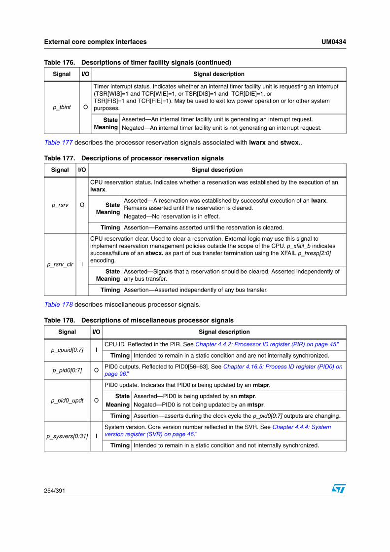
External core complex interfaces UM0434
254/391
Table 177 describes the processor reservation signals associated with lwarx and stwcx..
Table 178 describes miscellaneous processor signals.
p_tbint O
Timer interrupt status. Indicates whether an internal timer facility unit is requesting an interrupt (TSR[WIS]=1 and TCR[WIE]=1, or TSR[DIS]=1 and TCR[DIE]=1, or TSR[FIS]=1 and TCR[FIE]=1). May be used to exit low power operation or for other system purposes.
StateMeaning
Asserted—An internal timer facility unit is generating an interrupt request.Negated—An internal timer facility unit is not generating an interrupt request.
Table 176. Descriptions of timer facility signals (continued)
Signal I/O Signal description
Table 177. Descriptions of processor reservation signals
Signal I/O Signal description
p_rsrv O
CPU reservation status. Indicates whether a reservation was established by the execution of an lwarx.
StateMeaning
Asserted—A reservation was established by successful execution of an lwarx. Remains asserted until the reservation is cleared.
Negated—No reservation is in effect.
Timing Assertion—Remains asserted until the reservation is cleared.
p_rsrv_clr I
CPU reservation clear. Used to clear a reservation. External logic may use this signal to implement reservation management policies outside the scope of the CPU. p_xfail_b indicates success/failure of an stwcx. as part of bus transfer termination using the XFAIL p_hresp[2:0] encoding.
StateMeaning
Asserted—Signals that a reservation should be cleared. Asserted independently of any bus transfer.
Timing Assertion—Asserted independently of any bus transfer.
Table 178. Descriptions of miscellaneous processor signals
Signal I/O Signal description
p_cpuid[0:7] ICPU ID. Reflected in the PIR. See Chapter 4.4.2: Processor ID register (PIR) on page 45.”
Timing Intended to remain in a static condition and are not internally synchronized.
p_pid0[0:7] OPID0 outputs. Reflected to PID0[56–63]. See Chapter 4.16.5: Process ID register (PID0) on page 96.”
p_pid0_updt O
PID0 update. Indicates that PID0 is being updated by an mtspr.
StateMeaning
Asserted—PID0 is being updated by an mtspr.Negated—PID0 is not being updated by an mtspr.
Timing Assertion—asserts during the clock cycle the p_pid0[0:7] outputs are changing.
p_sysvers[0:31] I
System version. Core version number reflected in the SVR. See Chapter 4.4.4: System version register (SVR) on page 46.”
Timing Intended to remain in a static condition and not internally synchronized.

UM0434 External core complex interfaces
255/391
9.3.1 Processor state signals
Table 179 describes the processor state signals.
p_pvrin[16:31] I
Processor version. Provide a portion of the version number for a particular CPU. Reflected in the PVR. See Chapter 4.4.3: Processor version register (PVR) on page 45.”
Timing Intended to remain in a static condition and are not internally synchronized.
Table 178. Descriptions of miscellaneous processor signals (continued)
Signal I/O Signal description
Table 179. Descriptions of processor state signals
Signal I/O Signal description
p_pstat[0:6] O
Processor status. Indicate the internal execution unit status. Any values not shown are reserved.
p_pstat[0:6]Internal Processor Status00000xx Execution stalled
00001xx Execute exception
00010xx Instruction squashed
01000xx Processor in halted state01001xx Processor in stopped state
01010xx Processor in debug mode(1)
01011xx Processor in checkstop state10000sm Complete instruction(2),(3)
1000100 Complete lmw or stmw1000101 Complete e_lmw or e_stmw1001000 Complete isync1001011 Complete se_isync100110m Complete lwarx or stwcx. 3
1100000 Complete branch instruction bc, bcl, bca, bcla, b, bl, ba, bla resolved as not taken
1100001 Complete branch instruction e_bc, e_bcl, e_b, e_bl resolved as not taken
1100011 Complete branch instruction se_bc, se_bcl, se_b, se_bl resolved as not taken1100100 Complete branch instruction bc, bcl, bca, bcla, b, bl, ba, bla resolved as taken
1100101 Complete branch instruction e_bc, e_bcl, e_b, e_bl resolved as taken
1100111 Complete branch instruction se_bc, se_bcl, se_b, se_bl resolved as taken1101000 Complete bclr, bclrl, bcctr, bcctrl resolved as not taken
1101100 Complete bclr, bclrl, bcctr, bcctrl resolved as taken
1101111 Complete se_blr, se_blrl, se_bctr, se_bctrl (always taken)111000m Complete isel with condition false
111010m Complete isel with condition true
1111100 Complete rfi, rfci, or rfdi1111111 Complete se_rfi, se_rfci, or se_rfdi
TimingSynchronous with m_clk, so the indicated status may not apply to a current bus transfer.
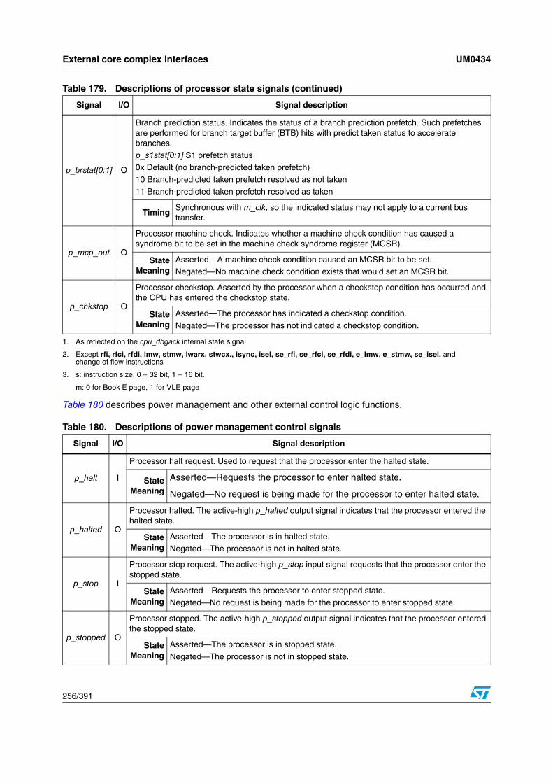
External core complex interfaces UM0434
256/391
Table 180 describes power management and other external control logic functions.
p_brstat[0:1] O
Branch prediction status. Indicates the status of a branch prediction prefetch. Such prefetches are performed for branch target buffer (BTB) hits with predict taken status to accelerate branches.
p_s1stat[0:1] S1 prefetch status0x Default (no branch-predicted taken prefetch)
10 Branch-predicted taken prefetch resolved as not taken
11 Branch-predicted taken prefetch resolved as taken
TimingSynchronous with m_clk, so the indicated status may not apply to a current bus transfer.
p_mcp_out O
Processor machine check. Indicates whether a machine check condition has caused a syndrome bit to be set in the machine check syndrome register (MCSR).
StateMeaning
Asserted—A machine check condition caused an MCSR bit to be set.
Negated—No machine check condition exists that would set an MCSR bit.
p_chkstop O
Processor checkstop. Asserted by the processor when a checkstop condition has occurred and the CPU has entered the checkstop state.
StateMeaning
Asserted—The processor has indicated a checkstop condition.
Negated—The processor has not indicated a checkstop condition.
1. As reflected on the cpu_dbgack internal state signal
2. Except rfi, rfci, rfdi, lmw, stmw, lwarx, stwcx., isync, isel, se_rfi, se_rfci, se_rfdi, e_lmw, e_stmw, se_isel, and change of flow instructions
3. s: instruction size, 0 = 32 bit, 1 = 16 bit.
m: 0 for Book E page, 1 for VLE page
Table 179. Descriptions of processor state signals (continued)
Signal I/O Signal description
Table 180. Descriptions of power management control signals
Signal I/O Signal description
p_halt I
Processor halt request. Used to request that the processor enter the halted state.
StateMeaning
Asserted—Requests the processor to enter halted state.
Negated—No request is being made for the processor to enter halted state.
p_halted O
Processor halted. The active-high p_halted output signal indicates that the processor entered the halted state.
StateMeaning
Asserted—The processor is in halted state.
Negated—The processor is not in halted state.
p_stop I
Processor stop request. The active-high p_stop input signal requests that the processor enter the stopped state.
StateMeaning
Asserted—Requests the processor to enter stopped state. Negated—No request is being made for the processor to enter stopped state.
p_stopped O
Processor stopped. The active-high p_stopped output signal indicates that the processor entered the stopped state.
StateMeaning
Asserted—The processor is in stopped state.
Negated—The processor is not in stopped state.

UM0434 External core complex interfaces
257/391
Table 181 describes signal debug events to the core.
p_dozep_nap
p_sleepO
Low-power mode. Asserted by the processor to reflect the settings of HID0[DOZE,NAP,SLEEP] when MSR[WE] is set. The core can be placed in a low-power state by forcing m_clk to a quiescent state and brought out of low-power state by re-enabling m_clk. The time base facilities may be separately enabled or disabled using combinations of the timer facility control signals. External logic can detect the asserted edge or level of these signals to determine which low-power mode has been requested and then place the core and peripherals in a low-power consumption state. p_wakeup can be monitored to determine when to end the low-power condition.
StateMeaning
Asserted—MSR[WE] and the respective HID0 bit are both set.
Negated—MSR[WE] and the respective HID0 bit are not both set.
Timing Assertion—May assert for 1 or more clock cycles.
p_wakeup O
Wake up. Used by external logic to remove the core and system logic from a low-power state. It can also indicate to the system clock controller that m_clk should be re-enabled for debug purposes.
p_wakeup (or other system state) should be monitored to determine when to release the processor (and system if applicable) from a low-power state.
StateMeaning
Asserted—Asserts whenever one of the following occurs: – A valid pending interrupt is detected by the core.
– A request to enter debug mode is made by setting the OCR[DR] or via the assertion of jd_de_b or p_ude.
– The processor is in a debug session and jd_debug_b is asserted.
– A request to enable m_clk has been made by setting OCR[WKUP].
TimingSee Chapter 9.5.5: Power management on page 289.” This signal is asynchronous to the system clock and should be synchronized to the system clock domain to avoid hazards.
Table 180. Descriptions of power management control signals (continued)
Signal I/O Signal description
Table 181. Descriptions of debug events signals
Signal I/O Signal description
p_ude I
Unconditional debug event. Used to request an unconditional debug event.
StateMeaning
Asserted—An unconditional debug event has been requested. Only a transition from negated to asserted state of p_ude causes an event to occur. However, the level on this signal causes assertion of p_wakeup.
Negated—No unconditional debug event has been requested.
Timing
Not internally synchronized by the core, and must meet setup and hold time constraints relative to m_clk when the core clock is running.
Assertion—Level-sensitive and must be held asserted until acknowledged by software, or, when external debug mode is enabled, by assertion of jd_debug_b to be guaranteed recognition. Only a transition from negated to asserted state of p_ude causes an event to occur. However, the level on this signal causes assertion of p_wakeup.
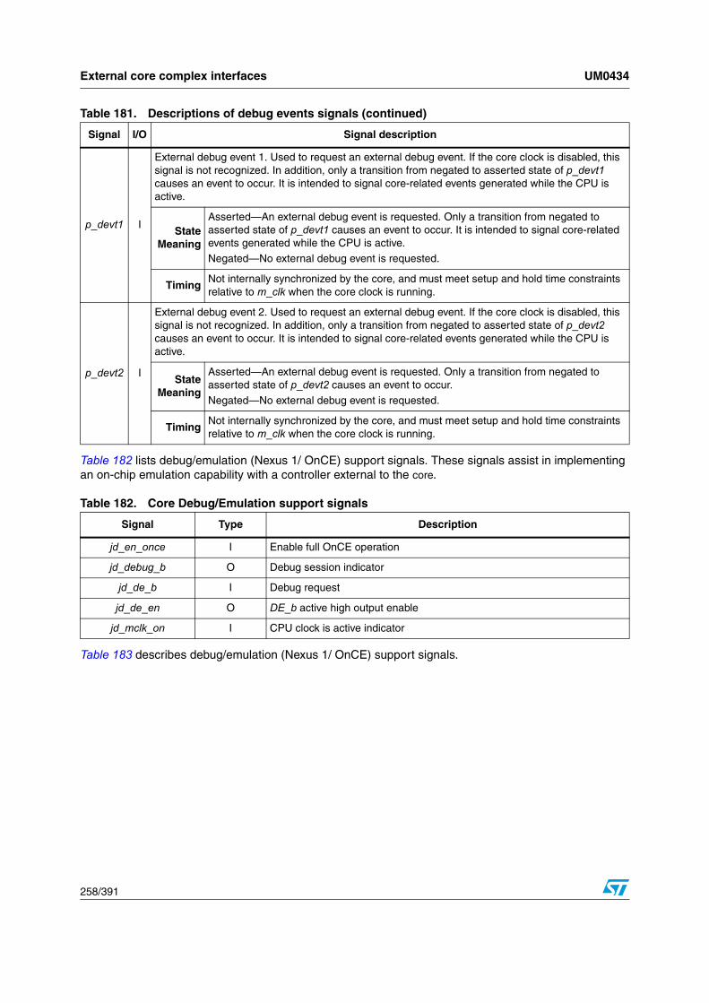
External core complex interfaces UM0434
258/391
Table 182 lists debug/emulation (Nexus 1/ OnCE) support signals. These signals assist in implementing an on-chip emulation capability with a controller external to the core.
Table 183 describes debug/emulation (Nexus 1/ OnCE) support signals.
p_devt1 I
External debug event 1. Used to request an external debug event. If the core clock is disabled, this signal is not recognized. In addition, only a transition from negated to asserted state of p_devt1 causes an event to occur. It is intended to signal core-related events generated while the CPU is active.
StateMeaning
Asserted—An external debug event is requested. Only a transition from negated to asserted state of p_devt1 causes an event to occur. It is intended to signal core-related events generated while the CPU is active.
Negated—No external debug event is requested.
TimingNot internally synchronized by the core, and must meet setup and hold time constraints relative to m_clk when the core clock is running.
p_devt2 I
External debug event 2. Used to request an external debug event. If the core clock is disabled, this signal is not recognized. In addition, only a transition from negated to asserted state of p_devt2 causes an event to occur. It is intended to signal core-related events generated while the CPU is active.
StateMeaning
Asserted—An external debug event is requested. Only a transition from negated to asserted state of p_devt2 causes an event to occur.
Negated—No external debug event is requested.
TimingNot internally synchronized by the core, and must meet setup and hold time constraints relative to m_clk when the core clock is running.
Table 181. Descriptions of debug events signals (continued)
Signal I/O Signal description
Table 182. Core Debug/Emulation support signals
Signal Type Description
jd_en_once I Enable full OnCE operation
jd_debug_b O Debug session indicator
jd_de_b I Debug request
jd_de_en O DE_b active high output enable
jd_mclk_on I CPU clock is active indicator

UM0434 External core complex interfaces
259/391
Table 183. Descriptions of Debug/Emulation (Nexus 1/ OnCE) support signals
Signal I/O Signal description
jd_en_once I
OnCE enable. Enables the OnCE controller to allow certain instructions and operations to be executed. Other systems should tie this signal asserted to enable full OnCE operation. j_en_once_regsel and j_key_in are provided to assist external logic performing security checks.
StateMeaning
Asserted—Enables the full OnCE command set, as well as operation of control signals and OnCE control register functions.
Negated—Only the bypass, ID, and Enable_OnCE commands are executed by the OnCE unit; all other commands default to a bypass command. The OnCE status register (OSR) is not visible when OnCE operation is disabled. In addition, OCR functions and the operation of jd_de_b are disabled. Secure systems may leave this signal negated until a security check is performed.
TimingMust change state only during the test-logic-reset, run-test/idle, or update_dr TAP states. A new value takes effect after one additional j_tclk cycle of synchronization.
jd_debug_b O
Debug session. A debug session includes single-step operations (Go+NoExit OnCE commands). This signal is provided to inform system resources that access is occurring for debug purposes, thus allowing certain resource side effects to be frozen or otherwise controlled. Examples may include FIFO state change control and control of side-effects of register or memory accesses. See Chapter 11.5.4: OnCE interface signals on page 309.”
StateMeaning
Asserted—Asserted when the processor enters debug mode. It remains asserted for the duration of a debug session. that is, during OnCE single-step executions.
jd_de_b I
Debug request. Normally the input from the top-level DE_b open-drain bidirectional I/O cell. See Chapter 11.5.4: OnCE interface signals on page 309.”
StateMeaning
Asserted—A debug request is pending. Negated—No debug request is pending.
Timing
Assertion—Not internally synchronized by the core and must meet setup and hold time constraints relative to j_tclk. To be recognized, it must be held asserted for a minimum of two j_tclk periods, and jd_en_once must be in the asserted state. jd_de_b is synchronized to m_clk in the debug module before being sent to the processor (two clocks).
jd_de_en O
DE_b active high output enable. Enable for the top-level DE_b open-drain bidirectional I/O cell. See Chapter 11.5.4: OnCE interface signals on page 309.”
StateMeaning
Asserted—the top-level DE_b open-drain bidirectional I/O cell is enabled.
Negated—the top-level DE_b open-drain bidirectional I/O cell is disabled.
TimingAssertion—Asserted for three j_tclk periods upon processor entry into debug mode.
jd_mclk_on I
Processor clock on. Driven by system-level clock control logic to indicate the m_clk input state
StateMeaning
Asserted—The processor’s m_clk input is active.
Negated—The processor’s m_clk input is not active.
Timing Assertion—Synchronized to j_tclk and provided as an OSR status bit.
jd_watchpoint[0:7] O
Watchpoint events. Indicate whether a watchpoint occurred. Each debug address compare function (IAC1–IAC4, DAC1–DAC2), and debug counter event (DCNT1–DCNT2) is capable of triggering a watchpoint output.
StateMeaning
Asserted—A watchpoint occurred
Negated—No watchpoint occurred

External core complex interfaces UM0434
260/391
Table 184 lists interface signals that assist in implementing a real-time development tool capability with a controller that is external to the core. These signals are described in Chapter 12.11: Nexus3 pin interface on page 371.”
Table 185 lists the primary JTAG interface signals. These signals are usually connected directly to device pins (except for j_tdo, which needs tri-state and edge support logic), unless JTAG TAP controllers are concatenated.
Table 186 describes JTAG interface signals.
Table 184. core development support (Nexus3) signals
Signal Type Description
nex_mcko O Nexus3 clock output
nex_rdy_b O Nexus3 ready output
nex_evto_b O Nexus3 event-out output
nex_evti_b I Nexus3 event-in input
nex_mdo[n:0] O Nexus3 message data output
nex_mseo_b[1:0] O Nexus3 message start/end output
Table 185. JTAG primary interface signals
Signal name Type Description
j_trst_b I JTAG test reset
j_tclk I JTAG test clock
j_tms I JTAG test mode select
j_tdi I JTAG test data input
j_tdo O Test data out to master controller or pad
j_tdo_en OEnables TDO output buffer. j_tdo_en is asserted when the TAP controller is in the shift_dr or shift_ir state.
Table 186. Descriptions of JTAG interface signals
Signal I/O Signal description
j_tdi IJTAG/OnCE serial input. Provides data and commands to the OnCE controller. Data is latched on the rising edge of j_tclk. Data is shifted into the OnCE serial port lsb first.
j_tclk I
JTAG/OnCE serial clock. Supplies the serial clock to the OnCE control block. The serial clock provides pulses required to shift data and commands into and out of the OnCE serial port (data is clocked into the OnCE on the rising edge and is clocked out of the OnCE serial port on the rising edge). The debug serial clock frequency must not exceed 50% of the processor clock frequency.

UM0434 External core complex interfaces
261/391
j_tdo O
JTAG/OnCE serial output. Serial data is read from the OnCE block through j_tdo.
StateMeaning
Data is shifted out the OnCE serial port lsb first.
Timing
When data is clocked out of the OnCE serial port, j_tdo changes on the rising edge of j_tclk. The j_tdo output is always driven. An external system-level TDO pin may be three-statable and should be actively driven in the shift-IR and shift-DR controller states. j_tdo_en indicates when an external TDO pin should be enabled, and is asserted during the shift-IR and shift-DR controller states. In addition, for IEEE1149 compliance, the system-level pin should change state on the falling edge of TCLK.
j_tms IJTAG/OnCE test mode select. Used to cycle through states in the OnCE debug controller. Toggling j_tms while clocking with j_tclk controls transitions through the TAP state controller.
j_trst_b I
JTAG/OnCE test reset. Resets the OnCE controller externally by placing it in the test-logic-reset state. The following information details additional signals that can support external JTAG data registers using the core TAP controller.Signal Name Type Descriptionj_tst_log_rst O Indicates the TAP controller is in the test-logic-reset statej_rti O JTAG controller run-test/idle statej_capture_ir O Indicates the TAP controller is in the capture IR statej_shift_ir O Indicates the TAP controller is in shift IR statej_update_ir O Indicates the TAP controller is in update IR statej_capture_dr O Indicates the TAP controller is in the capture DR statej_shift_dr O Indicates the TAP controller is in shift DR statej_update_gp_reg O Updates JTAG controller general-purpose data registerj_gp_regsel[0:11] O General-purpose external JTAG register selectj_en_once_regsel O External enable OnCE register selectj_key_in I Serial data from external key logicj_nexus_regsel O External Nexus register selectj_lsrl_regsel O External LSRL register selectj_serial_data I Serial data from external JTAG register(s)
j_tst_log_rst O
Test-logic-reset. Indicates whether the TAP controller is in test-logic-reset state.
StateMeaning
Asserted—The TAP controller is in test-logic-reset state. Negated—The TAP controller is not in test-logic-reset state.
j_rti O
Run-test/idle. Indicates whether the TAP controller is in the run-test/idle state.
StateMeaning
Asserted—The TAP controller is in run-test/idle state.
Negated—The TAP controller is not in run-test/idle state.
j_capture_ir O
Capture IR. Indicates whether the TAP controller is in the Capture_IR state.
StateMeaning
Asserted—The TAP controller is in Capture_IR state.
Negated—The TAP controller is not in Capture_IR state.
j_shift_ir O
Shift IR. Indicates whether the TAP controller is in the Shift_IR state.
StateMeaning
Asserted—The TAP controller is in Shift_IR state. Negated—The TAP controller is not in Shift_IR state.
Table 186. Descriptions of JTAG interface signals (continued)
Signal I/O Signal description

External core complex interfaces UM0434
262/391
j_update_ir O
Update IR. Indicates the TAP controller is in the Update_IR state.
StateMeaning
Asserted—The TAP controller is in Update_IR state. Negated—The TAP controller is not in Update_IR state.
j_capture_dr O
Capture DR. Indicates whether the TAP controller is in the Capture_DR state.
StateMeaning
Asserted—The TAP controller is in Capture_DR state.
Negated—The TAP controller is not in Capture_DR state.
j_shift_dr O
Shift DR. Indicates whether the TAP controller is in the Shift_DR state.
StateMeaning
Asserted—The TAP controller is in Shift_DR state.
Negated—The TAP controller is not in Shift_DR state.
j_update_gp_reg O
Update DR. Indicates whether the TAP controller is in the Update_DR state.
StateMeaning
Asserted—The TAP controller is in the Update_DR state, and OCMD[R/W] is low (write command). j_gp_regsel[0:11] should be monitored to see which register, if any, needs updating. Negated—The TAP controller is not in the Update_DR state.
j_gp_regsel O
Register select. Decoded from the OCMD[RS]. They are used to specify which external general-purpose JTAG register to access using the core TAP controller.
Signal Name Type RSj_gp_regsel[0] O 0x70j_gp_regsel[1] O 0x71j_gp_regsel[2] O 0x72j_gp_regsel[3] O 0x73j_gp_regsel[4] O 0x74j_gp_regsel[5] O 0x75j_gp_regsel[6] O 0x76j_gp_regsel[7] O 0x77j_gp_regsel[8] O 0x78j_gp_regsel[9] O 0x79j_gp_regsel[10] O 0x7Aj_gp_regsel[11] O 0x7B
j_en_once_regsel O
Enable once register select. This control signal can be used by external security logic to help control jd_enable_once. The external enable_OnCE register should be muxed onto the j_serial_data input. During the Shift_DR state, j_serial_data is supplied to j_tdo.
StateMeaning
Asserted—A decode of OCMD[RS] indicates an external enable_OnCE register is selected (0b1111110 encoding) for access using the core TAP controller.
j_nexus_regsel O
External Nexus register select.
StateMeaning
Asserted—A decode of OCMD[RS] indicates an external Nexus register is selected (0b1111100 encoding) for access using the core TAP controller. Negated—No Nexus register is selected.
j_lsrl_regsel O
LSRL register select.
StateMeaning
Asserted—A decode of OCMD[RS] indicates an external LSRL register is selected (0b1111101 encoding) for access using the core TAP controller.
Table 186. Descriptions of JTAG interface signals (continued)
Signal I/O Signal description

UM0434 External core complex interfaces
263/391
Figure 32 shows an example for designing an external JTAG register set using the inputs and outputs provided along with the JTAG primary inputs. The main components are a clock generation unit, a JTAG shifter (load, shift, hold, clr), the registers (load, hold, clr), and an input mux to the shifter for the serial output back to the core.The shifter and the registers may be as wide as the application warrants [0:x]. The length determines the number of states the TAP controller is held in Shift_DR (x+1).
Figure 32. Example external JTAG register design
9.3.2 JTAG ID signals
Table 187 shows the JTAG ID register unique to Freescale as specified by the IEEE 1149.1 JTAG Specification. Note that bit 31 is the msb of this register.
j_serial_data ISerial data. Receives serial data from external JTAG registers. All external registers share this serial output back to the core. Therefore it must be muxed using j_gp_regsel[0:11], j_lsrl_regsel, and j_en_once_regsel. The data is internally routed to j_tdo.
j_key_in I
Key data in. Receives serial data from logic to indicate a key or other value to be scanned out in the Shift_IR state when the current value in the IR is the Enable_OnCE instruction. This input is provided to assist in implementing security logic outside of the core, which conditionally asserts jd_en_once. During the Shift_IR state, when jd_en_once is negated, this input is sampled on the rising edge of j_tclk, and, after a 2-clock delay, the data is internally routed to j_tdo. This allows provision of a key value via the j_tdo output following a transition from Capture_IR to Shift_IR. j_key_in provides the key value.
Table 186. Descriptions of JTAG interface signals (continued)
Signal I/O Signal description
Shifter
D
Data
Q
REG0Q
D REG1Q
j_gp_regsel[1:0] S
D
01
reg0_dat
reg1_dat
clk_reg0 2
clk_reg13
2. clk_reg0 = j_tclk & j_update_gp_reg & j_gp_regsel[0]3. clk_reg1 = j_tclk & j_update_gp_reg & j_gp_regsel[1]
SI
SOj_serial_data
j_tdi
clk_shfter 1
1. clk_shfter = j_tclk & (j_shift_dr | j_capture_dr)
CLKGEN
j_tclk
j_gp_regsel[1:0]
j_shift_dr
j_update_gp_reg
SHIFTLOAD
j_capture_dr
j_shift_drj_capture_dr
j_trst_b
NOTES:

External core complex interfaces UM0434
264/391
The core shifts out a 1 as the first bit on j_tdo if the Shift_DR state is entered directly from the test-logic-reset state, per the JTAG specification, and informs any JTAG controller that an ID register exists on the part. The JTAG ID register is accessed by writing the OCMR (OnCE command register) with the value 0x02 in OCMD[RS].
The JTAG ID bit, manufacturer ID field, and design center number are fixed by the JTAG Consortium or Freescale. The version numbers and the 2 msbs of the sequence number are variable and brought out to external ports. The 8 lsbs of the sequence number are variable and are strapped internally to track variations in processor deliverables.
Table 188 shows the inputs to the JTAG ID register that are input ports on the core. These bits can help a customer track revisions of a device using the core.
Table 189 describes the JTAG ID signals.
Table 187. JTAG register ID fields
Bit field Type Description Value
[31:28] Variable Version number Variable
[27:22] Fixed Design center number (e200z3) 01_1111
[21:12] Variable Sequence number Variable
[11:1] Fixed Motorola manufacturer ID 000_0000_1110
0 Fixed JTAG ID register identification bit 1
Table 188. JTAG ID register inputs
Signal name Type Description
j_id_sequence[0:1] I JTAG ID register (2 msbs of sequence field)
j_id_version[0:3] I JTAG ID register version field
Table 189. Descriptions of JTAG ID signals
Signal I/O Signal description
j_id_sequence[0:1] I
JTAG ID sequence. Corresponds to the two msbs of the 10-bit sequence number in the JTAG ID register. These inputs are normally static and are provided for the integrator for further component variation identification.
j_id_sequence[2:9] I
JTAG ID sequence. Internally strapped by EPS to track variations in processor and module deliverables. Each core deliverable has a unique sequence number. Additionally, each revision of these modules can be identified by unique sequence numbers. EPS maintains a database of the sequence numbers.
j_id_version[0:3] IJTAG ID version. Corresponds to the 4-bit version number in the JTAG ID register. These inputs are normally static. They are provided to the customer for strapping to facilitate identification of component variants.

UM0434 External core complex interfaces
265/391
9.4 Internal signalsTable 190 lists internal signals that are mentioned in this manual. These signals are not directly accessible to the user, but are used in this document to help describe the general behavior of the core.
9.5 Timing diagramsThe following sections discuss various types of timing diagrams.
9.5.1 Processor Instruction/Data transfers
Transfer of data between the core and peripherals involves the address bus, data buses, and control and attribute signals. The address and data buses are parallel, non-multiplexed buses, supporting byte, half word, 3-byte, word, and double-word transfers. All bus inputs and outputs are sampled and driven with respect to the rising edge of m_clk. The core moves data on the bus by issuing control signals and using a handshake protocol to ensure correct data movement.
The memory interface operates in a pipelined fashion to allow additional access time for memory and peripherals. AHB transfers consist of an address phase that lasts only one cycle, followed by the data phase that may last for one or more cycles, depending on the state of p_[d,i]_hready.
Table 190. Internal signal descriptions
Signal name Description
p_addr[0:31] Address bus. Provides the address for a bus transfer.
p_ta_b
Transfer acknowledge. Indicates completion of a requested data transfer operation. An external device asserts p_ta_b to terminate the transfer. For the core to accept the transfer as successful, p_tea_b must remain high while p_ta_b is asserted.
p_tea_b
Transfer error acknowledge. Indicates that a transfer error condition has occurred and causes the core to immediately terminate the transfer. An external device asserts p_tea_b to terminate the transfer with error. p_tea_b has higher priority than p_ta_b.
p_treq_b Transfer request. The core drives this output to indicate that a new access has been requested.
p_xfail_b
Store exclusive failure. An external agent causes assertion of p_xfail_b to indicate a failure of the store portion of an stwcx. for the current transfer. p_xfail_b is ignored if p_tea_b is asserted, because the store terminated with an error. Assertion of p_xfail_b with p_ta_b does not cause an exception; it indicates that the store was not performed due to a loss of reservation (determined by an external agent). The CPU updates the condition code accordingly and clears any outstanding reservation. p_xfail_b may be asserted by reservation logic or as a result of a system bus transfer with a failure response that is passed back to the CPU from the BIU. The AMBA XFAIL response is signaled back to the CPU using this signal. See Chapter 5.7: Memory synchronization and reservation instructions on page 111.” p_xfail_b is ignored for all transfers other than an stwcx..

External core complex interfaces UM0434
266/391
Read transfers consist of the following:
● A request cycle, where address and attributes are driven along with a transfer request
● One or more memory access cycles to perform accesses and return data to the CPU for alignment, sign or zero extension, and forwarding.
Write transfers consist of a request cycle, in which address and attributes are driven along with a transfer request; and of one or more data drive cycles, in which write data is driven and external devices accept write data for the access.
To support sustained single-cycle transfers, access requests can overlap. Up to two access requests may be in progress during any cycle—one access outstanding and a second in the pending request phase. If access retraction is enabled via HID1[ARD] = 0, the BIU is free to change the current request at any time, even if part of a burst transfer.
Access requests are assumed to be accepted as long as either no access is in progress or an access is terminated during the same cycle when a new request is active (p_[d,i]_hready asserted). When an access is accepted, the BIU is free to change the current request.
The local memory control logic is responsible for proper pipelining and latching of all interface signals to initiate memory accesses.
The system hardware can use p_hresp[2:0] to signal, using the ERROR response encoding, that the current bus cycle has an error when a fault is detected. ERROR assertion requires a 2-cycle response. In the first cycle of the response, p_hresp[2:0] are driven to indicate ERROR and p_[d,i]_hready must be negated. During the following cycle, the ERROR response must continue to be driven, and p_[d,i]_hready must be asserted. When the core recognizes a bus error condition for an access at the end of the first cycle of the 2-cycle error response, a subsequent pending access request may be removed by the BIU driving p_[d,i]_htrans[2:0] to the IDLE state in the second cycle of the 2-cycle error response. Not all pending requests are removed, however.
When a bus cycle is terminated with a bus error, the core can enter storage error exception processing immediately following the bus cycle, or it can defer processing the exception.
The instruction prefetch mechanism requests instruction words from the instruction memory unit before it is ready to execute them. If a bus error occurs on an instruction fetch, the core does not take the exception until it attempts to use the instruction. Should an intervening instruction cause a branch, or should a task switch occur, the storage error exception for the unused access does not occur. A bus error termination for any write access or read access that references data specifically requested by the execution unit causes the core to begin exception processing.
Basic read transfer cycles
During a read transfer, the core receives data from a memory or peripheral device. Figure 33 shows functional timing for basic read transfers, and clock-by-clock descriptions of activity follow.

UM0434 External core complex interfaces
267/391
Figure 33. Basic read Transfer—Single-Cycle reads, full pipelining
● Clock 1 (C1)—The first read transfer starts in clock cycle 1. During C1, the core places valid values on the address bus and transfer attributes. The burst type (p_[d,i]_hburst[2:0]), protection control (p_[d,i]_hprot[5:0]), and transfer type (p_[d,i]_htrans[1:0]) attributes identify the specific access type. The transfer size attributes (p_[d,i]_hsize[1:0]) indicate the size of the transfer. The byte strobes (p_[d,i]_hbstrb[7:0]) are driven to indicate active byte lanes. The write (p_[d,i]_hwrite) signal is driven low for a read cycle.
The core asserts a transfer request (p_[d,i]_htrans= NONSEQ) during C1 to indicate that a transfer is being requested. Because the bus is currently idle, (0 transfers outstanding), the first read request to addrx is considered taken at the end of C1. The default slave drives a ready/OKAY response for the current idle cycle.
● Clock 2 (C2)—During C2, the addrx memory access takes place, using the address and attribute values that were driven during C1 to enable reading of 1 or more bytes of memory. Read data from the slave device is provided on the p_[d,i]_hrdata inputs. The slave device responds by asserting p_[d,i]_hready to indicate that the cycle is completing, and it drives an OKAY response.
Another read transfer request is made during C2 to addry (p_[d,i]_htrans = NONSEQ), and because the access to addrx is completing, it is considered taken at the end of C2.
● Clock 3 (C3)—During C3, the addry memory access takes place, using the address and attribute values that were driven during C2 to enable reading of one or more bytes of memory. Read data from the slave device for addry is provided on the p_[d,i]_hrdata inputs. The slave device responds by asserting p_[d,i]_hready to indicate the cycle is completing, and it drives an OKAY response.
Another read transfer request is made during C3 to addrz (p_[d,i]_htrans = NONSEQ), and because the access to addry is completing, it is considered taken at the end of C3.
● Clock 4 (C4)—During C4, the addrz memory access takes place, using the address and attribute values that were driven during C3 to enable reading of one or more bytes
nonseq nonseq nonseq idle
addr x addr y addr z
single single single
data x data y data z
okay okay okay okay
1 2 3 4 5m_clk
p_htrans
p_addr,p_hprot
p_hsize,
p_hbstrb, etc
p_hburst
p_hunalign
p_hwrite
p_hrdata
p_hwdata
p_hready
p_hresp

External core complex interfaces UM0434
268/391
of memory. Read data from the slave device for addrz is provided on the p_[d,i]_hrdata inputs. The slave device responds by asserting p_[d,i]_hready to indicate the cycle is completing, and it drives an OKAY response.
Because the CPU has no additional outstanding requests, p_[d,i]_htrans indicates IDLE and the address and attribute signals are undefined.
Read transfer with wait state
Figure 34 shows an example of wait state operation. Because signal p_[d,i]_hready for the first request (addrx) is not asserted during C2, a wait state is inserted until p_[d,i]_hready is recognized (during C3).
Meanwhile, a subsequent request was generated by the CPU for addry which is not taken in C2, because the previous transaction is still outstanding. The address and transfer attributes remain driven in cycle C3 and are taken at the end of C3 because the previous access is completing. Data for addrx and a ready/OKAY response are driven back by the slave device. In cycle C4, a request for addrz is made. The request for access to addrz is taken at the end of C4, and during C5, the slave device provides the data and a ready/OKAY response. In cycle C5, no further accesses are requested.
Figure 34. Read with Wait-State, Single-Cycle reads, full pipelining
Basic write transfer cycles
During a write transfer, the core provides write data to a memory or peripheral device. Figure 35 shows functional timing for basic write transfers. Clock-by-clock descriptions of activity in Figure 35 follow.
nonseq nonseq nonseq idle
addr x addr y addr z
single single single
data x data y data z
okay okay okay okay okay
1 2 3 4 5 6m_clk
p_htrans
p_addr,p_hprot
p_hsize,
p_hbstrb, etc
p_hburst
p_hunalign
p_hwrite
p_hrdata
p_hwdata
p_hready
p_hresp

UM0434 External core complex interfaces
269/391
Figure 35. Basic write Transfers—Single-Cycle writes, full pipelining
● Clock 1 (C1)—The first write transfer starts in clock cycle 1. During C1, the core places valid values on the address bus and transfer attributes. The burst type (p_[d,i]_hburst[2:0]), protection control (p_[d,i]_hprot[5:0]), and transfer type (p_[d,i]_htrans[1:0]) attributes identify the specific access type. The transfer size attributes (p_[d,i]_hsize[1:0]) indicate the size of the transfer. The byte strobes (p_[d,i]_hbstrb[7:0]) are driven to indicate active byte lanes. The write (p_[d,i]_hwrite) signal is driven high for a write cycle. The core asserts transfer request (p_[d,i]_htrans= NONSEQ) during C1 to indicate that a transfer is being requested. Because the bus is idle, (0 transfers outstanding), the first read request to addrx is considered taken at the end of C1. The default slave drives a ready/OKAY response for the current idle cycle.
● Clock 2 (C2)—During C2, the write data for the access is driven and the addrx memory access occurs using the address and attribute values (driven during C1) to enable writing of one or more bytes of memory. The slave device responds by asserting p_[d,i]_hready to indicate the cycle is completing and drives an OKAY response.
Another write transfer request is made during C2 to addry (p_[d,i]_htrans = NONSEQ), and because the access to addrx is completing, it is considered taken at the end of C2.
● Clock 3 (C3)—During C3, write data for addry is driven, and the addry memory access takes place using the address and attribute values (driven during C2) to enable writing of one or more bytes of memory. The slave device responds by asserting p_[d,i]_hready to indicate the cycle is completing and drives an OKAY response.
Another write transfer request is made during C3 to addrz (p_[d,i]_htrans = NONSEQ), and because the access to addry is completing, it is considered taken at the end of C3.
● Clock 4 (C4)—During C4, write data for addrz is driven, and the addrz memory access takes place using the address and attribute values (driven during C3) to enable reading of one or more bytes of memory. The slave device responds by asserting p_[d,i]_hready to indicate the cycle is completing and drives an OKAY response.
Because the CPU has no more outstanding requests, p_[d,i]_htrans indicates IDLE and the address and attribute signals are undefined.
nonseq nonseq nonseq idle
addr x addr y addr z
single single single
data x data y data z
okay okay okay okay
1 2 3 4 5m_clk
p_htrans
p_addr,p_hprot
p_hsize,
p_hbstrb, etc
p_hburst
p_hunalign
p_hwrite
p_hrdata
p_hwdata
p_hready
p_hresp

External core complex interfaces UM0434
270/391
Write transfer with wait states
Figure 36 shows an example write wait state operation. Because p_[d,i]_hready for the first request (addrx) is not asserted during C2, a wait state is inserted until p_[d,i]_hready is recognized (during C3).
Figure 36. Write with Wait-state, Single-Cycle writes, full pipelining
Meanwhile, the core generates a subsequent request for addry which is not taken in C2, because the previous transaction is outstanding. The address, transfer attributes, and write data remain driven in cycle C3 and are taken at the end of C3 because a ready/OKAY response is driven back by the slave device for the previous access. In cycle C4, a request for addrz is made. The request for access to addrz is taken at the end of C4, and during C5, the slave device provides a ready/OKAY response. In C5, no further accesses are requested.
nonseq nonseq nonseq idle
addr x addr y addr z
single single single
data x data y data z
okay okay okay okay okay
1 2 3 4 5 6m_clk
p_htrans
p_addr,p_hprot
p_hsize,
p_hbstrb, etc
p_hburst
p_hunalign
p_hwrite
p_hrdata
p_hwdata
p_hready
p_hresp

UM0434 External core complex interfaces
271/391
Read and write transfers
Figure 37 shows a sequence of read and write cycles.
Figure 37. Single-Cycle reads, Single-Cycle write, full pipelining
The first read request (addrx) is taken at the end of cycle C1 because the bus is idle. The second read request (addry) is taken at the end of C2 because a ready/OKAY response is asserted during C2 for the first read access (addrx). During C3, a request is generated for a write to addry which is taken at the end of C3 because the second access is terminating.
Data for the addrz write cycle is driven in C4, the cycle after the access is taken, and a ready/OKAY response is signaled to complete the write cycle to addrz.
nonseq nonseq nonseq idle
addr x addr y addr z
single single single
data x data y
data z
okay okay okay okay
1 2 3 4 5m_clk
p_htrans
p_addr,p_hprot
p_hsize,
p_hbstrb, etc
p_hburst
p_hunalign
p_hwrite
p_hrdata
p_hwdata
p_hready
p_hresp

External core complex interfaces UM0434
272/391
Figure 38 shows another sequence of read and write cycles. This example shows an interleaved write access between two reads.
Figure 38. Single-Cycle read, write, Read—Full pipelining
The first read request (addrx) is taken at the end of cycle C1 because the bus is idle. The first write request (addry) is taken at the end of C2 because the first access is terminating (addrx). Data for the addry write cycle is driven in C3, the cycle after the access is taken. Also during C3, a request is generated for a read to addrz, which is taken at the end of C3 because the write access is terminating.
During C4, the addry write access is terminated, and no further access is requested.
nonseq nonseq nonseq idle
addr x addr y addr z
single single single
data x data z
data y
okay okay okay okay
1 2 3 4 5m_clk
p_htrans
p_addr,p_hprot
p_hsize,
p_hbstrb, etc
p_hburst
p_hunalign
p_hwrite
p_hrdata
p_hwdata
p_hready
p_hresp

UM0434 External core complex interfaces
273/391
Figure 39 shows another sequence of read and write cycles. In this example, reads incur a single wait state.
Figure 39. Multiple-Cycle reads with Wait-State, Single-Cycle writes, full pipelining
The first read request (addrx) is taken at the end of cycle C1 because the bus is idle. The second read request (addry) is not taken at the end of cycle C2 because no ready response is signaled and only one access can be outstanding (addrx). It is taken at the end of C3 once the first read request has signaled a ready/OKAY response.
The first write request (addrz) is not taken during C4 because a ready response is not asserted during C4 for the second read access (addry). During C5, the request for a write to addrz is taken because the second access is terminating.
Data for the addrz write cycle is driven in C6, the cycle after the access is taken. During C6, the addrz write access is terminated and the addrw write request is taken.
During C7, data for the addrw write access is driven, and a ready/OKAY response is asserted to complete the write cycle to addrw.
nonseq nonseq nonseq nonseq idle
addr x addr y addr z addr w
single single single single
data x data y
data z data w
okay okay okay okay okay okay okay
1 2 3 4 5 6 7 8m_clk
p_htrans
p_addr,p_hprot
p_hsize,
p_hbstrb, etc
p_hburst
p_hunalign
p_hwrite
p_hrdata
p_hwdata
p_hready
p_hresp

External core complex interfaces UM0434
274/391
Figure 40 shows another sequence of read and write cycles. In this example, reads incur a single wait state.
Figure 40. Multi-Cycle read with Wait-State, Single-Cycle write, read with Wait-State, Single-Cycle write, full pipelining -
The first read request (addrx) is taken at the end of cycle C1 because the bus is idle.
The first write request (addry) is not taken at the end of cycle C2 because no ready response is signaled and only one access can be outstanding (addrx). It is taken at the end of C3 once the first read request has signaled a ready/OKAY response.
Data for the addry write cycle is driven in C4, the cycle after the access is taken. The second read request (addrz) is taken during C4 because the addry write is terminating.
A second write request (addrw) is not taken at the end of C5 because the second read access is not terminating, and it continues to drive the address and attributes into cycle C6. During C6, the addrz read access is terminated and the addrw write access is taken.
In cycle C7, data for the addrw write access is driven. During C7, a ready/OKAY response is asserted to complete the write cycle to addrw. No further accesses are requested, so p_[d,i]_htrans signals IDLE.
nonseq nonseq nonseq nonseq idle
addr x addr y addr z addr w
single single single single
data x data z
data y data w
okay okay okay okay okay okay okay
1 2 3 4 5 6 7 8m_clk
p_htrans
p_addr,p_hprot
p_hsize,
p_hbstrb, etc
p_hburst
p_hunalign
p_hwrite
p_hrdata
p_hwdata
p_hready
p_hresp

UM0434 External core complex interfaces
275/391
Misaligned accesses
Figure 41 shows functional timing for a misaligned read transfer. The read to addrx is misaligned across a 64-bit boundary. Note that only half-word and word transfers may be misaligned; double-word transfers are always aligned.
Figure 41. Misaligned read, read, full pipelining
The first portion of the misaligned read transfer starts in C1. During C1, the core places valid values on the address bus and transfer attributes. The p_[d,i]_hwrite signal is driven low for a read cycle. The transfer size attributes (p_[d,i]_hsize) indicate the size of the transfer. Even though the transfer is misaligned, the size value driven corresponds to the size of the entire misaligned data item. p_[d,i]_hunalign is driven high to indicate that the access is misaligned. The p_[d,i]_hbstrb outputs are asserted to indicate the active byte lanes for the read, which may not correspond to size and low-order address outputs. p_[d,i]_htrans is driven to NONSEQ.
During C2, the addrx memory access takes place using the address and attribute values which were driven during C1 to enable reading of one or more bytes of memory.
The second portion of the misaligned read transfer request is made during C2 to addrx+ (which is aligned to the next higher 64-bit boundary), and because the first portion of the misaligned access is completing, it is taken at the end of C2. The p_[d,i]_htrans signals indicate NONSEQ. The size value driven is the size of the remaining bytes of data in the misaligned read, rounded up (for the 3-byte case) to the next higher power of 2. The p_[d,i]_hbstrb signals indicate the active byte lanes. For the second portion of a misaligned transfer, p_[d,i]_hunalign is driven high for the 3-byte case (low for all others). The next read access is requested in C3 and p_[d,i]_htrans indicates NONSEQ. p_[d,i]_hunalign is negated, because this access is aligned.
nonseq nonseq nonseq idle
addr x addr x+ addr y
single single single
**
data x data x+ data y
okay okay okay okay
1 2 3 4 5m_clk
p_htrans
p_addr,p_hprot
p_hsize,
p_hbstrb, etc
p_hburst
p_hunalign
p_hwrite
p_hrdata
p_hwdata
p_hready
p_hresp

External core complex interfaces UM0434
276/391
Figure 42 shows functional timing for a misaligned write transfer. The write to addrx is misaligned across a 64-bit boundary. Note that only half-word and word transfers may be misaligned; double-word transfers are always aligned.
Figure 42. Misaligned write, write, full pipelining
The first portion of the misaligned write transfer starts in C1. During C1, the core places valid values on the address bus and transfer attributes. The p_[d,i]_hwrite signal is driven high for a write cycle. The transfer size attribute (p_[d,i]_hsize) indicates the size of the transfer. Even though the transfer is misaligned, the size value driven corresponds to the size of the entire misaligned data item. p_[d,i]_hunalign is driven high to indicate that the access is misaligned. The p_[d,i]_hbstrb outputs are asserted to indicate the active byte lanes for the write, which may not correspond to size and low-order address outputs. p_[d,i]_htrans is driven to NONSEQ.
During C2, data for addrx is driven, and the addrx memory access takes place using the address and attribute values that were driven during C1 to enable writing of one or more bytes of memory.
The second portion of the misaligned write transfer request is made during C2 to addrx+ (which is aligned to the next higher 64-bit boundary), and because the first portion of the misaligned access is completing, it is taken at the end of C2. The p_[d,i]_htrans signals indicate NONSEQ. The size value driven is the size of the remaining bytes of data in the misaligned write, rounded up (for the 3-byte case) to the next higher power-of-2. The p_[d,i]_hbstrb signals indicate the active byte lanes. For the second portion of a misaligned transfer, p_[d,i]_hunalign is driven high for the 3-byte case (low for all others).
The next write access is requested in C3 and p_[d,i]_htrans indicates NONSEQ. p_[d,i]_hunalign is negated, because this access is aligned.
nonseq nonseq nonseq idle
addr x addr x+ addr y
single single single
**
data x data x+ data y
okay okay okay okay
1 2 3 4 5m_clk
p_htrans
p_addr,p_hprot
p_hsize,
p_hbstrb, etc
p_hburst
p_hunalign
p_hwrite
p_hrdata
p_hwdata
p_hready
p_hresp

UM0434 External core complex interfaces
277/391
An example of a misaligned write cycle followed by an aligned read cycle is shown in Figure 43. It is similar to the example in Figure 42.
Figure 43. Misaligned write, single cycle read transfer, full pipelining
9.5.2 Burst accesses
Figure 44 shows functional timing for a burst read transfer.
Figure 44. Burst read transfer
nonseq nonseq nonseq idle
addr x addr x+ addr y
single single single
**
data y
data x data x+
okay okay okay okay
1 2 3 4 5m_clk
p_htrans
p_addr,p_hprot
p_hsize,
p_hbstrb, etc
p_hburst
p_hunalign
p_hwrite
p_hrdata
p_hwdata
p_hready
p_hresp
nonseq seq seq seq ...
addr x addr x+8 addr x+16 addr x+24
INCR
data x data x+8 data x+16 data x+24
okay okay okay okay okay
Burst Read 1 2 3 4 5 6
m_clk
p_htrans
p_addr,p_hprot
p_hsize,
p_hbstrb, etc
p_hburst
p_hunalign
p_hwrite
p_hrdata
p_hwdata
p_hready
p_hresp

External core complex interfaces UM0434
278/391
The p_[d,i]_hburst signals indicate INCR for all burst transfers. The p_[d,i]_hunalign signal is negated. p_[d,i]_hsize indicates 64-bits, and all eight p_[d,i]_hbstrb signals are asserted. The burst address is aligned to a 64-bit boundary and increments by double words. Note that in this example four beats are shown, but in operation the burst may be of any length including only a single beat.
Note: Bursts can be interrupted immediately at any time and can be followed by any type of cycle. No idle cycle is required.
Figure 45 shows functional timing for a burst read with wait-state transfer.
Figure 45. Burst read with Wait-state transfer
The first cycle of the burst incurs a single wait-state.
nonseq seq seq seq ...
addr x addr x+8 addr x+16 addr x+24
incr
data x data x+8 data x+16 data x+24
okay okay okay okay okay okay
Burst Read with wait-state1 2 3 4 5 6 7
m_clk
p_htrans
p_addr,p_hprot
p_hsize,
p_hbstrb, etc
p_hburst
p_hunalign
p_hwrite
p_hrdata
p_hwdata
p_hready
p_hresp

UM0434 External core complex interfaces
279/391
Figure 46 shows functional timing for a burst write transfer.
Figure 46. Burst write transfer
Figure 45 shows functional timing for a burst write with wait-state transfer.
Figure 47. Burst write with Wait-State transfer
nonseq seq seq seq ...
addr x addr x+8 addr x+16 addr x+24
incr
data x data x+8 data x+16 data x+24
okay okay okay okay okay
Burst Write1 2 3 4 5 6
m_clk
p_htrans
p_addr,p_hprot
p_hsize,
p_hbstrb, etc
p_hburst
p_hunalign
p_hwrite
p_hrdata
p_hwdata
p_hready
p_hresp
nonseq seq seq seq ...
addr x addr x+8 addr x+16 addr x+24
incr
data x data x+8 data x+16 data x+24
okay okay okay okay okay okay
Burst Write with Wait-state1 2 3 4 5 6 7
m_clk
p_htrans
p_addr,p_hprot
p_hsize,
p_hbstrb, etc
p_hburst
p_hunalign
p_hwrite
p_hrdata
p_hwdata
p_hready
p_hresp

External core complex interfaces UM0434
280/391
The first cycle of the burst incurs a single wait-state. Data for the second beat of the burst is valid the cycle after the second beat is taken.
Figure 48 shows functional timing for a pair of burst read transfers.
Figure 48. Burst read transfers
Note that in this example the first burst is two beats long and is followed immediately by a second burst which is unrelated to the first.
Note: Bursts may be of any length (including a single beat) and may be followed immediately by any type of transfer. No idle cycles are required.
nonseq seq nonseq seq ...
addr x addr x+8 addr y addr y+8
incr
data x data x+8 data y data y+8
okay okay okay okay okay
Burst Read 1 2 3 4 5 6
m_clk
p_htrans
p_addr,p_hprot
p_hsize,
p_hbstrb, etc
p_hburst
p_hunalign
p_hwrite
p_hrdata
p_hwdata
p_hready
p_hresp

UM0434 External core complex interfaces
281/391
Figure 49 shows functional timing for a burst read with wait-state transfer where the second beat to addr x+8 is retracted and replaced with a new burst transfer.
Figure 49. Burst read with Wait-State transfer, retraction
The 1st cycle of the burst incurs a single wait state, & the burst is replaced by another burst.
Figure 50 shows functional timing for a burst write transfer. The 2nd burst is only 1 beat long.
Figure 50. Burst write transfers, Single-Beat burst
This same scenario can occur for read bursts as well.
nonseq seq seq seq idle
addr x addr y+8 addr y+16
incr
data x data y data y+8 data y+16
okay okay okay okay okay okay
Burst Read with wait-state1 2 3 4 5 6 7
m_clk
p_htrans
p_addr,p_hprot
p_hsize,
p_hbstrb, etc
p_hburst
p_hunalign
p_hwrite
p_hrdata
p_hwdata
p_hready
p_hresp
addr yaddr x+8
nonseq
nonseq seq seq nonseq idle
addr x addr x+8 addr x+16 addr y
incr
data x data x+8 data x+16 data y
okay okay okay okay okay
Burst Write1 2 3 4 5 6
m_clk
p_htrans
p_addr,p_hprot
p_hsize,
p_hbstrb, etc
p_hburst
p_hunalign
p_hwrite
p_hrdata
p_hwdata
p_hready
p_hresp

External core complex interfaces UM0434
282/391
9.5.3 Address retraction
Address retraction is the process of replacing a request with a new unrelated one. Although the AMBA AHB protocol requires an access request to remain driven unchanged once presented on the bus, higher system performance may be obtained if this aspect of the protocol is modified to allow an access request to be changed before being taken. Figure 57 shows an example of address retraction during wait state operation. Signal p_[d,i]_hready for the first request (addrx) is not asserted during C2, so a wait state is inserted during C3 until p_[d,i]_hready is recognized.
Meanwhile, a subsequent request has been generated by the CPU for addry which is not taken in C2 since the previous transaction is still outstanding. The address and transfer attributes are retracted in cycle C3, and a new access request to addrz is requested and are taken at the end of C3 because the previous access is completing. Data for addrx and a ready/OKAY response is driven back by the slave device. In cycle C4, a request for addrw is made. The request for access to addrw is taken at the end of C4; during C5, the data and a ready/OKAY response is provided by the slave device. In cycle C5, no further accesses are requested.
Figure 51. Read transfer with Wait-State, address retraction
Figure 52 shows functional timing for a burst read with wait-state transfer where the second beat to addr x+8 is retracted and replaced with a new burst transfer.
nonseq nonseq nonseq idle
addr x addr y addr w
single single single
data x data z data w
okay okay okay okay okay
Read with wait-state, address retraction1 2 3 4 5 6
m_clk
p_htrans
p_addr,p_hprot
p_hsize,
p_hbstrb, etc
p_hburst
p_hunalign
p_hwrite
p_hrdata
p_hwdata
p_hready
p_hresp
addr z
nonseq

UM0434 External core complex interfaces
283/391
Figure 52. Burst read with Wait-State transfer, retraction
The first cycle of the burst incurs a single wait-state, and the burst is replaced by another burst. Replacement by a single access is also possible.
Address retraction does not occur on a requested write cycle, only on read cycles. It also may occur any time during a burst cycle.
Error termination operation
The p_[d,i]_hresp[2:0] inputs signal an error termination for an access in progress. The ERROR encoding is used with the assertion of p_[d,i]_hready to terminate a cycle with error. Error termination is a two-cycle termination; the first cycle consists of signaling the ERROR response on p_[d,i]_hresp[2:0] while holding p_[d,i]_hready negated, and during the second cycle, asserting p_[d,i]_hready while continuing to drive the ERROR response on p_[d,i]_hresp[2:0]. This 2-cycle termination allows the BIU to retract a pending access if it desires to do so. p_[d,i]_htrans may be driven to IDLE during the second cycle of the two-cycle error response, or may change to any other value, and a new access unrelated to the pending access may be requested. The cycle that may have been previously pending while waiting for a response that terminates with error may be changed. It is not required to remain unchanged when an error response is received.
nonseq seq seq seq idle
addr x addr y+8 addr y+16
incr
data x data y data y+8 data y+16
okay okay okay okay okay okay
Burst Read with wait-state1 2 3 4 5 6 7
m_clk
p_htrans
p_addr,p_hprot
p_hsize,
p_hbstrb, etc
p_hburst
p_hunalign
p_hwrite
p_hrdata
p_hwdata
p_hready
p_hresp
addr yaddr x+8
nonseq

External core complex interfaces UM0434
284/391
Figure 53 shows an example of error termination.
Figure 53. Read and write Transfers: instruction read with error, data read, write, full pipelining
The first read request (addrx) is taken at the end of cycle C1 because the bus is idle. It is an instruction prefetch.
The second read request (addry) is not taken at the end of C2 because the first access is still outstanding (no p_[d,i]_hready assertion). An error response is signaled by the addressed slave for addrx by driving ERROR onto the p_[d,i]_hresp[2:0] inputs. This is the first cycle of the two cycle error response protocol.
p_[d,i]_hready is asserted during C3 for the first read access (addrx) while the ERROR encoding remains driven on p_[d,i]_hresp[2:0], terminating the access. The read data bus is undefined.
In this example of error termination, the CPU continues to request an access to addry. It is taken at the end of C3. During C4, read data is supplied for the addry read, and the access is terminated normally during C4.
Also during C4, a request is generated for a write to addrz, which is taken at the end of C4 because the second access is terminating.
Data for the addrz write cycle is driven in C5, the cycle after the access is taken.
During C5, a ready/OKAY response is signaled to complete the write cycle to addrz.
In this example of error termination, a subsequent access remained requested. This does not always occur when certain types of transfers are terminated with error. The following figures outline cases where an error termination for a given cycle causes a pending request to be aborted prior to initiation.
Figure 54 shows another example of error termination.
nonseq nonseq nonseq idle
addr x addr y addr z
single single single
data x data y
data z
okay error error okay okay
1 2 3 4 5 6m_clk
p_htrans
p_addr,p_hprot
p_hsize,
p_hbstrb, etc
p_hburst
p_hunalign
p_hwrite
p_hrdata
p_hwdata
p_hready
p_hresp

UM0434 External core complex interfaces
285/391
Figure 54. Data read with error, data write retracted, instruction read, full pipelining
The first read request (addrx) is taken at the end of cycle C1 because the bus is idle. It is a data read.
The second request (write to addry) is not taken at the end of C2 because the first access is still outstanding (no p_[d,i]_hready assertion). An error response is signaled by the addressed slave for addrx by driving ERROR onto the p_[d,i]_hresp[2:0] inputs. This is the first cycle of the two cycle error response protocol.
p_[d,i]_hready is asserted during C3 for the first read access (addrx) while the ERROR encoding remains driven on p_[d,i]_hresp[2:0], terminating the access. The read data bus is undefined.
In this example of error termination, the CPU retracts the requested access to addry by driving p_[d,i]_htrans signals to the IDLE state during the second cycle of the two-cycle error response.
A different access to addrz is requested during C4 and is taken at the end of C4. During C5, read data is supplied for the addrz read, and the access is terminated normally.
In this example of error termination, a subsequent access was aborted.
nonseq nonseq idle nonseq idle
addr x addr y addr z
single single single
data x data z
okay error error okay okay
1 2 3 4 5 6m_clk
p_htrans
p_addr,p_hprot
p_hsize,
p_hbstrb, etc
p_hburst
p_hunalign
p_hwrite
p_hrdata
p_hwdata
p_hready
p_hresp

External core complex interfaces UM0434
286/391
Figure 55 shows another example of error termination, this time on the initial portion of a misaligned write.
Figure 55. Misaligned write with error, data write retracted, burst read substituted, full pipelining
The first portion of the misaligned write request is terminated with error. The second portion is aborted by the CPU during the second cycle of the two cycle error response, and a subsequent burst read access to addrw becomes pending instead.
nonseq nonseq idle nonseq seq seq seq idle
addr x addr x+ addr w addr w+8 addr w+16 addr w+24
single single wrap 4
**
data w w+8 w+16 w +24
data x
okay error error okay okay okay okay okay
1 2 3 4 5 6 7 8m_clk
p_htrans
p_addr,p_hprot
p_hsize,
p_hbstrb, etc
p_hburst
p_hunalign
p_hwrite
p_hrdata
p_hwdata
p_hready
p_hresp

UM0434 External core complex interfaces
287/391
Figure 56 shows another example of error termination, this time on the initial portion of a burst read. The aborted burst is followed by a burst write.
Figure 56. Burst read with error termination, burst write
The first portion of the burst read request is terminated with error. The second portion is aborted by the CPU during the second cycle of the two cycle error response, and a subsequent burst write access to addry becomes pending instead.
9.5.4 Address retraction
Address retraction is the process of replacing a request with a new unrelated one. Although the AMBA AHB protocol requires an access request to remain driven unchanged once presented on the bus, higher system performance may be obtained if this aspect of the protocol is modified to allow an access request to be changed before being taken. Figure 57 shows an example of address retraction during wait state operation. Signal p_hready for the first request (addrx) is not asserted during C2, so a wait state is inserted during C3 until p_hready is recognized.
Meanwhile, a subsequent request has been generated by the CPU for addry which is not taken in C2 since the previous transaction is still outstanding. The address and transfer attributes are retracted in cycle C3, and a new access to addrz is requested and made at the end of C3 because the previous access is completing. Data for addrx and a ready/OKAY response are driven back by the slave device. In cycle C4, a request for addrw is made. The request for access to addrw is taken at the end of C4; during C5, the data and a ready/OKAY response are provided by the slave device. In cycle C5, no further accesses are requested.
nonseq seq idle nonseq seq seq seq idle
addr x addr x+8 addr y addr y+8 addr y+16 addr y+24
wrap4 wrap4
data x
data y y+8 y+16 y+24
okay error error okay okay okay okay okay
1 2 3 4 5 6 7 8m_clk
p_htrans
p_addr,p_hprot
p_hsize,
p_hbstrb, etc
p_hburst
p_hunalign
p_hwrite
p_hrdata
p_hwdata
p_hready
p_hresp

External core complex interfaces UM0434
288/391
Figure 57. Read transfer with Wait-State, address retraction
Figure 58 shows functional timing for a burst read with wait-state transfer where the second beat to addr x+8 is retracted and replaced with a new burst transfer.
Figure 58. Burst read with Wait-State transfer, retraction
The first cycle of the burst incurs a single wait-state, and the burst is replaced by another burst. Replacement by a single access is also possible.
nonseq nonseq nonseq idle
addr x addr y addr w
single single single
data x data z data w
okay okay okay okay okay
Read with wait-state, address retraction1 2 3 4 5 6
m_clk
p_htrans
p_addr,p_hprot
p_hsize,
p_hbstrb, etc
p_hburst
p_hunalign
p_hwrite
p_hrdata
p_hwdata
p_hready
p_hresp
addr z
nonseq
nonseq seq seq seq idle
addr x addr y+8 addr y+16
incr
data x data y data y+8 data y+16
okay okay okay okay okay okay
Burst Read with wait-state1 2 3 4 5 6 7
m_clk
p_htrans
p_addr,p_hprot
p_hsize,
p_hbstrb, etc
p_hburst
p_hunalign
p_hwrite
p_hrdata
p_hwdata
p_hready
p_hresp
addr yaddr x+8
nonseq

UM0434 External core complex interfaces
289/391
Address retraction does not occur on a requested write cycle, only on read cycles. It also may occur any time during a burst cycle.
9.5.5 Power management
Figure 59 shows the relationship of the wake-up control signal p_wakeup to the relevant input signals.
Figure 59. Wakeup control signal (p_wakeup)
9.5.6 Interrupt interface
Figure 60 shows the relationship of the interrupt input signals to the CPU clock. The p_avec_b, p_extint_b, p_critint_b, and p_voffset[0:15] inputs must meet setup and hold timing relative to the rising edge of m_clk. In addition, during each clock cycle in which either p_extint_b or p_critint_b is asserted, p_avec_b and p_voffset[0:15] are required to be in a valid state for the highest priority interrupt requested.
Figure 60. Interrupt interface input signals
m_clk
p_extint_b
p_wakeup
p_critint_bjd_de_b,
p_ude,OCR[WKUP]
p_extint_b
p_voffset[0:15]
p_critint_bp_avec_b
m_clk
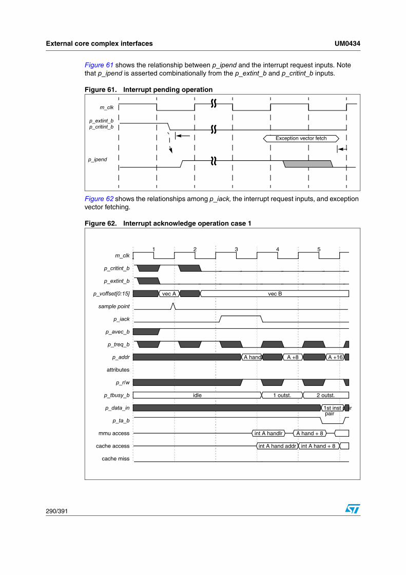
External core complex interfaces UM0434
290/391
Figure 61 shows the relationship between p_ipend and the interrupt request inputs. Note that p_ipend is asserted combinationally from the p_extint_b and p_critint_b inputs.
Figure 61. Interrupt pending operation
Figure 62 shows the relationships among p_iack, the interrupt request inputs, and exception vector fetching.
Figure 62. Interrupt acknowledge operation case 1
m_clk
p_extint_b
p_ipend
p_critint_b
Exception vector fetch
pair
vec A vec B
A handler A +8 A +16
idle 1 outst. 2 outst.
1st inst pair
int A handlr A hand + 8
int A hand addr int A hand + 8
1 2 3 4 5m_clk
p_critint_b
p_extint_b
p_voffset[0:15]
sample point
p_iack
p_avec_b
p_treq_b
p_addr
attributes
p_r/w
p_tbusy_b
p_data_in
p_ta_b
mmu access
cache access
cache miss

UM0434 External core complex interfaces
291/391
In this example, an external input interrupt is requested in cycle 1. The p_voffset[0:15] inputs are driven with the vector offset for ‘A’, and p_avec_b is negated, indicating vectoring is desired. For this example, the bus is idle at the time of assertion. The CPU may sample a requested interrupt as early as the cycle in which it is initially requested, and it does so in this example. The interrupt request,the vector offset, and the autovector input are sampled at the end of cycle 1. In cycle 3, the interrupt is acknowledged by the assertion of the p_iack output, indicating that the values present on interrupt inputs at the beginning of cycle 2 have been internally latched and committed for servicing. Note that the interrupt vector lines have changed to a value of ‘B’ during cycle 2, and the p_critint_b input has been asserted by the interrupt controller. The vector number and autovector signals must be consistent with the higher priority critical input request, and thus must change when the state of the interrupt request inputs change. The p_iack output assertion in cycle 3 indicates that the values present at the rise of cycle 2 (vector ‘A’) have been committed to. During cycle 3, the CPU begins instruction fetching of the handler for vector ‘A’. The new request for a subsequent critical interrupt ‘B’ was not received in time to be acted on first. It is acknowledged after the fetch for the external input interrupt handler is completed and has entered decode.
Note that the time between assertion of an interrupt request input and the acknowledgment of an interrupt may be multiple cycles, and the interrupt inputs may change during that interval. The CPU asserts the p_iack output to indicate the cycle at which an interrupt is committed to. In the following example, because the CPU was unable to acknowledge the external input interrupt during cycle 2 due to internal or external execution conditions, the critical input request was sampled. This case is shown in Figure 63.
Figure 63. Interrupt acknowledge operation case 2
vec A vec B
B handler B +8
idle 1 outst. 2 outst.
int B handlr B hand + 8
int B hand addr int B hand + 8
1 2 3 4 5m_clk
p_critint_b
p_extint_b
p_voffset[0:15]
sample point
p_iack
p_avec_b
p_treq_b
p_addr
attributes
p_r/w
p_tbusy_b
p_data_in
p_ta_b
mmu access
cache access
cache miss

Power management UM0434
292/391
10 Power management
This chapter describes the power management facilities as they are defined by Book E and implemented in devices that contain the core. The scope of this chapter is limited to core complex features. Additional power management capabilities associated with a device that integrates this core (referred to as an integrated device) are documented separately.
10.1 OverviewPower management minimizes overall system power consumption. The core provides the ability to initiate power management from external sources as well as through software techniques. Table 191 describes core power states.
Table 191. Power states
State Description
Active(Default)
All internal units on the core operate at full processor clock speed. The core provides dynamic power management in which idle internal units may stop clocking automatically.
Halted
Instruction execution and bus activity are suspended, and most internal clocks are gated off. The core asserts p_halted to indicate it is in the halted state. Before entering halted state, all outstanding bus transactions complete, and the cache’s store and push buffers are flushed. The m_clk input should remain running to allow further transitions into the power-down state if requested and to keep the time base operational if it is using m_clk as the clock source.
Power down
(stopped)
All core functional units except the time base unit and clock control state machine logic are stopped. m_clk may be kept running to keep the time base active and to allow quick recovery to full-on state. Clocks are not running to functional units except to the time base. The core reaches power-down state after transitioning through halted state with p_stop asserted; at this point p_stopped output is asserted.
Additional power may be saved by disabling the time base by asserting p_tbdisable or by integrated logic stopping m_clk after the core is in power-down state and has asserted p_stopped.
To exit power-down state, integrated logic must first restart m_clk.
Because the time base is off during power-down state, if m_clk is the clock source and is stopped, or if time base clocking is disabled by the assertion of p_tbdisable, system software must usually have to access an external time base source after returning to the full-on state to reinitialize the time base unit. A time-base related interrupt source (such as the decrementer) cannot be used to exit low-power states.
The core also provides the ability to clock the time base from an independent (but externally synchronized) clock source, which allows the time base to be maintained during the power-down state, and allows a time-base related interrupt to be generated to indicate an exit condition from the power-down state.

UM0434 Power management
293/391
Figure 64 is a power management state diagram.
Figure 64. Power management state diagram
10.1.1 Power management signals
Table 191 summarizes power management signals. More detailed information is provided in Chapter 9.5.5: Power management on page 289.”
Halted
Power-Down
~p_stop & p_halt
p_stop
~p_halt & ~p_stopp_halt | p_stop
~p_stopp_stop
Active ~p_halt & ~p_stop
(p_stopped asserted)
(p_halted asserted)
Table 192. Descriptions of timer facility and power management signals
Signal I/O Signal description
p_halt IProcessor halt request. The active-high p_halt input requests that the core enter the halted state.
p_halted OProcessor halted. The active-high p_halted output indicates that the core entered the halted state.
p_stop IProcessor stop request. The active-high p_stop input requests that the core enter the stopped state.
p_stopped OProcessor stopped. The active-high p_stopped output indicates that the core entered stopped state.
p_dozep_nap
p_sleepO
Low-power mode. These signals are asserted by the core to reflect the settings of the HID0[DOZE], HID0[NAP], and HID0[SLEEP] control bits when MSR[WE] is set. The core can be placed in a low-power state by forcing m_clk to a quiescent state, and brought out of low-power state by re-enabling m_clk. The time base facilities may be separately enabled or disabled using combinations of the timer facility control signals.
p_wakeup O
Wakeup. Used by external logic to remove the core and system logic from a low-power state. It can also indicate to the system clock controller that m_clk should be re-enabled for debug purposes.
p_wakeup (or other system state) should be monitored to determine when to release the core (and system if applicable) from a low-power state.
p_tbdisable ITimer disable. Used to disable the internal time base and decrementer counters. This signal can be used to freeze the state of the time base and decrementer during low power or debug operation.
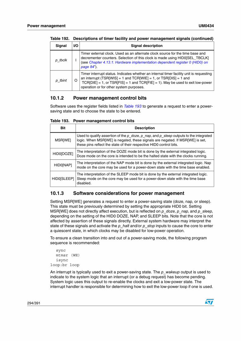
Power management UM0434
294/391
10.1.2 Power management control bits
Software uses the register fields listed in Table 193 to generate a request to enter a power-saving state and to choose the state to be entered.
10.1.3 Software considerations for power management
Setting MSR[WE] generates a request to enter a power-saving state (doze, nap, or sleep). This state must be previously determined by setting the appropriate HID0 bit. Setting MSR[WE] does not directly affect execution, but is reflected on p_doze, p_nap, and p_sleep, depending on the setting of the HID0 DOZE, NAP, and SLEEP bits. Note that the core is not affected by assertion of these signals directly. External system hardware may interpret the state of these signals and activate the p_halt and/or p_stop inputs to cause the core to enter a quiescent state, in which clocks may be disabled for low-power operation.
To ensure a clean transition into and out of a power-saving mode, the following program sequence is recommended:
syncmtmsr (WE)isync
loop:br loop
An interrupt is typically used to exit a power-saving state. The p_wakeup output is used to indicate to the system logic that an interrupt (or a debug request) has become pending. System logic uses this output to re-enable the clocks and exit a low-power state. The interrupt handler is responsible for determining how to exit the low-power loop if one is used.
p_tbclk I
Timer external clock. Used as an alternate clock source for the time base and decrementer counters. Selection of this clock is made using HID0[SEL_TBCLK] (see Chapter 4.13.1: Hardware implementation dependent register 0 (HID0) on page 84”).
p_tbint O
Timer interrupt status. Indicates whether an internal timer facility unit is requesting an interrupt (TSR[WIS] = 1 and TCR[WIE] = 1, or TSR[DIS] = 1 and TCR[DIE] = 1, or TSR[FIS] = 1 and TCR[FIE] = 1). May be used to exit low-power
operation or for other system purposes.
Table 193. Power management control bits
Bit Description
MSR[WE]Used to qualify assertion of the p_doze, p_nap, and p_sleep outputs to the integrated logic. When MSR[WE] is negated, these signals are negated. If MSR[WE] is set, these pins reflect the state of their respective HID0 control bits.
HID0[DOZE]The interpretation of the DOZE mode bit is done by the external integrated logic. Doze mode on the core is intended to be the halted state with the clocks running.
HID0[NAP]The interpretation of the NAP mode bit is done by the external integrated logic. Nap mode on the core may be used for a power-down state with the time base enabled.
HID0[SLEEP]The interpretation of the SLEEP mode bit is done by the external integrated logic. Sleep mode on the core may be used for a power-down state with the time base disabled.
Table 192. Descriptions of timer facility and power management signals (continued)
Signal I/O Signal description

UM0434 Power management
295/391
The vectored interrupt capability provided by the core may help determine whether an external hardware interrupt is used to perform the wake-up.
10.1.4 Debug considerations for power management
When a debug request is presented to the core when it is in either the halted or stopped state, p_wakeup is asserted, and when m_clk is provided to the CPU, it temporarily exits the halted or stopped state and enters debug mode, regardless of the assertion of p_halt or p_stop. The p_halted and p_stopped outputs are negated as long as the CPU remains in a debug session (jd_debug_b asserted). When the debug session is exited, the CPU resamples the p_halt and p_stop inputs and re-enters halted or stopped state as appropriate.

Debug support UM0434
296/391
11 Debug support
11.1 IntroductionThis chapter describes the debug features of the e200z3 core, including the software and hardware debug facilities, events, and registers. It also details the external debug support features available and introduces the reader to the on-chip emulation circuitry (OnCE) and its key attributes, that is, the interface signals, debug inputs, and outputs. This chapter also covers watchpoint support, MMU and cache operations during debug, cache array access, and the basic steps for enabling, using, and exiting external debug mode.
11.2 OverviewInternal debug support in the core allows for software and hardware debugging by providing debug functions such as instruction and data breakpoints and program trace modes. For software-based debugging, debug facilities consisting of a set of software-accessible debug registers and interrupt mechanisms are provided. These facilities are also available to a hardware-based debugger that communicates using a modified IEEE 1149.1 test access port (TAP) controller and pin interface. When hardware debugging is enabled, the debug facilities are protected from software modification.
Software debug facilities are defined as part of Book E. The core supports a subset of these defined facilities. In addition to the Book E–defined facilities, the core provides additional flexibility and functionality in the form of debug event counters, linked instruction and data breakpoints, and sequential debug event detection. These features are also available to a hardware-based debugger.
The core also supports an external Nexus real-time debug module. Real-time system-level debugging is supported by an external Nexus class 2, 3, or 4 module. Definitions and features of this module are part of the system/platform specification and are not further defined in this chapter. Additional information can be found in Chapter 12: Nexus3 module on page 329.”
11.2.1 Software debug facilities
The debug facilities enable hardware and software debug functions, such as instruction and data breakpoints and program single-stepping. The debug facilities consist of a set of debug control registers (DBCR0–DBCR3), a set of address compare registers (IAC1–IAC4, DAC1, and DAC2), a configurable debug counter register (DBCNT), a debug status register (DBSR) for enabling and recording various kinds of debug events, and a special debug interrupt type built into the interrupt mechanism (see Chapter 6.6.16: Debug interrupt (IVOR15) on page 180,” for more information). The debug facilities also provide mechanisms for software-controlled processor reset and for controlling the operation of the timers in a debug environment.
Software debug facilities are enabled by setting the internal debug mode bit, DBCR0[IDM]. If DBCR0[IDM] is set, debug events can occur and can be enabled to record exceptions in the DBSR. If enabled by MSR[DE], these exceptions cause debug interrupts. If DBCR0[IDM] and DBCR0[EDM] (EDM represents the external debug mode bit) are cleared, no debug events occur and no status flags are set in DBSR unless already set. In addition, if DBCR0[IDM] is cleared (or is overridden by DBCR0[EDM] being set), no debug interrupts can occur, regardless of the contents of DBSR. A software debug interrupt handler can

UM0434 Debug support
297/391
access all system resources and perform the necessary functions appropriate for system debugging.
PowerPC book E compatibility
The core implements a subset of the PowerPC Book E internal debug features. The following restrictions on functionality are present:
● Instruction address compares do not support compare on physical (real) addresses.
● Data address compares do not support compare on physical (real) addresses.
● Data value compares are not supported.
11.2.2 Additional debug facilities
In addition to the debug functionality defined in Book E, the core provides the capability to link instruction and data breakpoints. The core also provides a configurable debug event counter to allow debug exception generation and a sequential breakpoint control mechanism.
The core also defines two new debug events (critical interrupt taken and critical return) for debugging around critical interrupts.
In addition, the core implements the debug auxiliary processing unit (APU) which, when enabled, allows debug interrupts to use a dedicated set of save/restore registers (DSRR0 and DSRR1) to save state information when a debug interrupt occurs and restore this state information at the end of a debug interrupt handler with the rfdi instruction.
11.2.3 Hardware debug facilities
The core contains facilities that allow for external test and debugging. A modified IEEE 1149.1 control interface is used to communicate with core resources. This interface is implemented through a standard 1149.1 TAP (test access port) controller.
By using public instructions, the external debugger can freeze or halt the core, read and write internal state and debug facilities, single-step instructions, and resume normal execution.
Hardware debug is enabled by setting the external debug mode enable bit (DBCR0[EDM]). Setting DBCR0[EDM] overrides the internal debug mode enable bit DBCR0[IDM]. If the hardware debug facility is enabled, software is blocked from modifying the debug facilities. In addition, because resources are owned by the hardware debugger, inconsistent values may be present if software attempts to read debug-related resources.
When hardware debug is enabled (DBCR0[EDM] = 1), the registers and resources described in Chapter 11.3: Debug registers,” are reserved for use by the external debugger. The events described in Chapter 11.3: Debug registers,” are also used for external debugging, but exceptions are not generated to running software. Debug events enabled in the respective DBCR0–DBCR3 registers are recorded in the DBSR regardless of MSR[DE], and no debug interrupts are generated. Instead, the CPU enters debug mode when an enabled event causes a DBSR bit to become set. DBCR0[EDM] may only be written through the OnCE port.
A program trace program counter FIFO (PC FIFO) is also provided to support program change-of-flow capture.
To perform write accesses from the external hardware debugger, most debug resources (registers) require the CPU clock (m_clk) to be running.

Debug support UM0434
298/391
Figure 65 shows the core debug resources.
Figure 65. Core debug resources
11.3 Debug registersThe debug facility registers are listed in Table 194 and described in Chapter 4.12: Debug registers on page 69.”
Pstat#Attr#
Addr#j_tdo, j_tdo_en
j_tdi
j_tclk
Breakpoint andTrace Logic
Pipeline Information
j_tms
dbg_dbgrq
cpu_dbgack
jd_watchpt[0:n]
#internal signalsto/from CPU only
p_devt[1,2]
j_trst_b
jd_de_en jd_debug_b
Data#
jd_en_once
jd_de_b
jd_mclk_on
p_ude
PCFIFO
DebugRegisters
andComparators
OnCEController
andSerial
Interface
Table 194. Debug registers
Mnemonic NameSPR
numberAccess Privileged
Core specific
DBCR0 Debug control register 0 308 R/W Yes No
DBCR1 Debug control register 1 309 R/W Yes No
DBC.R2 Debug control register 2 310 R/W Yes No
DBCR3 Debug control register 3 561 R/W Yes Yes
DBSR Debug status register 304 Read/Clear(1) Yes No
DBCNT Debug counter register 562 R/W Yes Yes
IAC1 Instruction address compare 1 312 R/W Yes No

UM0434 Debug support
299/391
11.4 Software debug events and exceptionsSoftware debug events and exceptions are available if internal debug mode is enabled (DBCR0[IDM] = 1) and not overridden by external debug mode (DBCR0[EDM] = 0). When enabled, debug events cause debug exceptions to be recorded in the debug status register. Specific event types are enabled by DBCR0–DBCR3. The unconditional debug event (UDE) is an exception to this rule; it is always enabled. Once a DBSR bit other than MRR and CNT1TRG is set, if debug interrupts are enabled by MSR[DE], a debug interrupt is generated. The debug interrupt handler is responsible for ensuring that multiple repeated debug interrupts do not occur by clearing the DBSR as appropriate.
Certain debug events are not allowed to occur when MSR[DE] = 0 and DBCR0[EDM] = 0. Under these conditions, no debug exception occurs and thus no DBSR bit is set. Other debug events may cause debug exceptions and set DBSR bits regardless of the state of MSR[DE]. A debug interrupt is delayed until MSR[DE] is set.
When a DBSR bit is set while MSR[DE] = 0 and DBCR0[EDM] = 0, an imprecise debug event flag (DBSR[IDE]) is also set to indicate that an exception bit in the DBSR was set while debug interrupts were disabled. The debug interrupt handler software can use this bit to determine whether DSRR0 holds the address associated with the instruction causing the debug exception or the address of the instruction that enabled a delayed debug interrupt by setting MSR[DE]. An mtmsr or mtdbcr0, which causes both MSR[DE] and DBCR0[IDM] to be set, enabling precise debug mode, may cause an imprecise (delayed) debug exception to be generated due to an earlier recorded event in the DBSR.
The following types of debug events are defined by Book E:
● Instruction address compare debug events
● Data address compare debug events
● Trap debug events
● Branch taken debug events
● Instruction complete debug events
● Interrupt taken debug events
● Return debug events
● Unconditional debug events
These events are described in further detail in the EREF.
IAC2 Instruction address compare 2 313 R/W Yes No
IAC3 Instruction address compare 3 314 R/W Yes No
IAC4 Instruction address compare 4 315 R/W Yes No
DAC1 Data address compare 1 316 R/W Yes No
DAC2 Data address compare 2 317 R/W Yes No
1. The DBSR can be read using mfspr rD,DBSR. It cannot be directly written to. Instead, DBSR bits corresponding to 1 bits in GPR(rS) can be cleared using mtspr DBSR,rS.
Table 194. Debug registers (continued)
Mnemonic NameSPR
numberAccess Privileged
Core specific

Debug support UM0434
300/391
The core defines the following debug events, which are described in Table 195:
● The debug counter debug events DCNT1 and DCNT2
● The external debug events DEVT1 and DEVT2
● The critical interrupt taken debug event (CIRPT)
● The critical return debug event (CRET)
The core debug framework supports most of these event types. The following Book E–defined functionality is not supported:
● Instruction address compare and data address compare real address mode
● Data value compare mode
A brief description of each of the debug event types is shown in Table 195. In these descriptions, DSRR0 and DSRR1 are used to store the address of the instruction following a load or store, assuming that the debug APU is enabled. If it is disabled, CSRR0 is used.

UM0434 Debug support
301/391
Table 195. Debug event descriptions
Event name Type Description
Instruction Address Compare Event
IAC
Occurs when enabled and upon attempted execution of an instruction at an address that meets the criteria specified in the DBCR0, DBCR1,and IACn registers. Instruction address compares may specify user/supervisor mode and instruction space (MSR[IS]), along with an effective address, masked effective address, or range of effective addresses for comparison. This event can occur and be recorded in DBSR regardless of the setting of MSR[DE]. IAC events do not occur when an instruction would not have normally begun execution due to a higher priority exception at an instruction boundary.
IAC compares perform a 31-bit compare for VLE instruction pages, and 30-bit compares for BookE instruction pages. Each half-word fetched by the instruction fetch unit will be marked with a set of bits indicating whether an Instruction Address Compare occurred on that half-word. Debug exceptions will occur if enabled and a 16-bit instruction, or the first half-word of a 32-bit instruction, is tagged with an IAC hit. For instruction fetches that miss in the TLB, Book E pages are assumed, and a 30-bit compare is performed.
Data Address Compare Event
DAC
Data address compare debug events occur if data address compare debug events are enabled and execution of a load or store class instruction or a cache maintenance instruction results in a data access with an address that meets the criteria specified in DBCR0, DBCR2, DAC1, and DAC2. Data address compares may specify user/supervisor mode and data space (MSR[DS]), along with an effective address, masked effective address, or range of effective addresses for comparison. This event can occur and be recorded in DBSR regardless of the setting of MSR[DE]. Two address compare values (DAC1 and DAC2) are provided.
In contrast to the Book E definition, data address compare events on the core do not prevent the load or store instruction from completing. If a load or store class instruction completes successfully without a data TLB or data storage interrupt, data address compare exceptions are reported at the completion of the instruction. If the exception results in a precise debug interrupt, the address value saved in DSRR0 (or CSRR0 if the debug APU is disabled) is the address of the instruction following the load or store class instruction.
If a load or store class instruction does not complete successfully due to a data TLB or data storage exception, and a data address compare debug exception also occurs, the result is an imprecise debug interrupt, the address value saved in DSRR0 (or CSRR0 if the debug APU is disabled) is the address of the load or store class instruction, and DBSR[IDE] is set. In addition to occurring when DBCR0[IDM] = 1, this can also occur when DBCR0[EDM] = 1.
DAC events are not recorded or counted if an lmw or stmw instruction is interrupted before completion by a critical input or external input interrupt.
– DAC events are not signaled on the following:—The second portion of a misaligned load or store that is broken up into two separate accesses—The tlbre, tlbwe, tlbsx, or tlbivax instructions
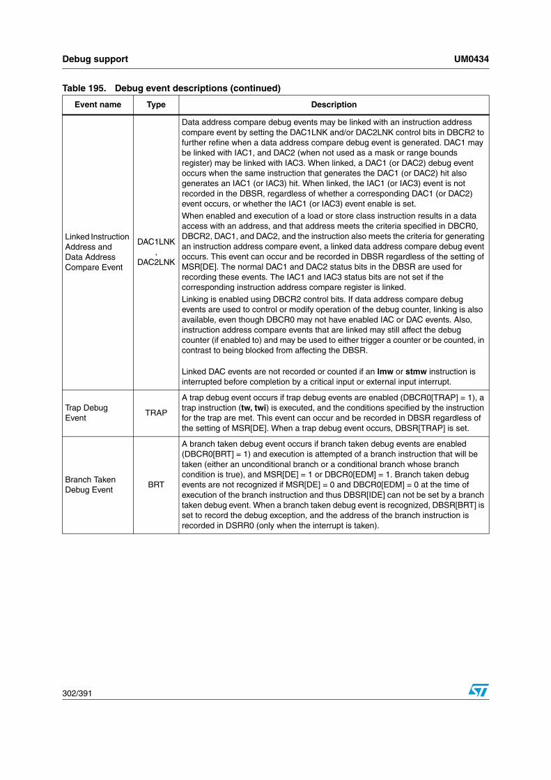
Debug support UM0434
302/391
Linked Instruction Address and Data Address Compare Event
DAC1LNK,
DAC2LNK
Data address compare debug events may be linked with an instruction address compare event by setting the DAC1LNK and/or DAC2LNK control bits in DBCR2 to further refine when a data address compare debug event is generated. DAC1 may be linked with IAC1, and DAC2 (when not used as a mask or range bounds register) may be linked with IAC3. When linked, a DAC1 (or DAC2) debug event occurs when the same instruction that generates the DAC1 (or DAC2) hit also generates an IAC1 (or IAC3) hit. When linked, the IAC1 (or IAC3) event is not recorded in the DBSR, regardless of whether a corresponding DAC1 (or DAC2) event occurs, or whether the IAC1 (or IAC3) event enable is set.
When enabled and execution of a load or store class instruction results in a data access with an address, and that address meets the criteria specified in DBCR0, DBCR2, DAC1, and DAC2, and the instruction also meets the criteria for generating an instruction address compare event, a linked data address compare debug event occurs. This event can occur and be recorded in DBSR regardless of the setting of MSR[DE]. The normal DAC1 and DAC2 status bits in the DBSR are used for recording these events. The IAC1 and IAC3 status bits are not set if the corresponding instruction address compare register is linked.
Linking is enabled using DBCR2 control bits. If data address compare debug events are used to control or modify operation of the debug counter, linking is also available, even though DBCR0 may not have enabled IAC or DAC events. Also, instruction address compare events that are linked may still affect the debug counter (if enabled to) and may be used to either trigger a counter or be counted, in contrast to being blocked from affecting the DBSR.
Linked DAC events are not recorded or counted if an lmw or stmw instruction is interrupted before completion by a critical input or external input interrupt.
Trap Debug Event
TRAP
A trap debug event occurs if trap debug events are enabled (DBCR0[TRAP] = 1), a trap instruction (tw, twi) is executed, and the conditions specified by the instruction for the trap are met. This event can occur and be recorded in DBSR regardless of the setting of MSR[DE]. When a trap debug event occurs, DBSR[TRAP] is set.
Branch Taken Debug Event
BRT
A branch taken debug event occurs if branch taken debug events are enabled (DBCR0[BRT] = 1) and execution is attempted of a branch instruction that will be taken (either an unconditional branch or a conditional branch whose branch condition is true), and MSR[DE] = 1 or DBCR0[EDM] = 1. Branch taken debug events are not recognized if MSR[DE] = 0 and DBCR0[EDM] = 0 at the time of execution of the branch instruction and thus DBSR[IDE] can not be set by a branch taken debug event. When a branch taken debug event is recognized, DBSR[BRT] is set to record the debug exception, and the address of the branch instruction is recorded in DSRR0 (only when the interrupt is taken).
Table 195. Debug event descriptions (continued)
Event name Type Description

UM0434 Debug support
303/391
Instruction Complete Debug Event
IAC
An instruction-complete debug event occurs if instruction-complete debug events are enabled (DBCR0[ICMP] = 1), execution of any instruction is completed, and MSR[DE] = 1 or DBCR0[EDM] = 1. If execution of an instruction is suppressed due to the instruction causing some other exception that is enabled to generate an interrupt, then the attempted execution of that instruction does not cause an instruction complete debug event. The sc instruction does not fall into the category of an instruction whose execution is suppressed, since the instruction actually executes and then generates a system call interrupt. In this case, the instruction complete debug exception is also set. When an instruction complete debug event is recognized, DBSR[ICMP] is set to record the debug exception, and the address of the next instruction to be executed is recorded in DSRR0.Instruction complete debug events are not recognized if MSR[DE] = 0 and DBCR0[EDM] = 0 at the time of execution of the instruction; thus, DBSR[IDE] is not generally set by an ICMP debug event.
One circumstance may cause DBSR[ICMP] and DBSR[IDE] to be set. This occurs when an embedded FPU round exception occurs. Because the instruction is by definition completed (SRR0 points to the following instruction), this interrupt takes higher priority than the debug interrupt so as not to be lost, and DBSR[IDE] = 1 to indicate imprecise recognition of a debug interrupt. In this case, the debug interrupt is taken with SRR0 pointing to the instruction following the instruction that generated the SPEFPU round exception, and DSRR0 points to the round exception handler. In addition to occurring when DBCR0[IDM] = 1, this circumstance can also occur when DBCR0[EDM] = 1.
Instruction complete debug events are not generated by the execution of an instruction that sets MSR[DE] while DBCR0[ICMP] = 1, nor by the execution of an instruction that sets DBCR0[ICMP] while MSR[DE] = 1 or DBCR0[EDM] = 1.
Interrupt Taken Debug Event
IRPT
An interrupt-taken debug event occurs if interrupt-taken debug events are enabled (DBCR0[IRPT] = 1) and a non-critical interrupt occurs. Only non-critical class interrupts cause an interrupt-taken debug event. This event can occur and be recorded in DBSR regardless of the setting of MSR[DE]. When an interrupt-taken debug event occurs, DBSR[IRPT] is set to record the debug exception. DSRR0 holds the address of the non-critical interrupt handler.
Critical Interrupt Taken Debug Event
CIRPT
A critical interrupt taken debug event occurs if critical interrupt taken debug events are enabled (DBCR0[CIRPT] = 1) and a critical interrupt (other than a debug interrupt when the debug APU is disabled) occurs. Only critical class interrupts cause a critical-interrupt-taken debug event. This event can occur and be recorded in DBSR regardless of the setting of MSR[DE]. When a critical-interrupt-taken debug event occurs, DBSR[CIRPT] bit is set, ensuring that debug exceptions are recorded. DSRR0 holds the address of the critical interrupt handler.
To avoid corruption of CSRR0 or CSRR1, this debug event should not normally be enabled unless the debug APU is also enabled.
Table 195. Debug event descriptions (continued)
Event name Type Description

Debug support UM0434
304/391
11.5 External debug supportExternal debug support is supplied through the core’s OnCE controller serial interface, which allows access to internal CPU registers and other system state while in external debug mode (DBCR0[EDM] is set). All debug resources, including DBCR0–DBCR3, DBSR, IAC1–IAC4, DAC1, DAC2 and DBCNT are accessible through the serial on-chip emulation (OnCE) interface in external debug mode. Setting the DBCR0[EDM] bit through the OnCE interface enables external debug mode and disables software updates to the debug registers. When DBCR0[EDM] is set, debug events enabled to set respective DBSR status
Return Debug Event
RET
A return debug event occurs if return debug events are enabled (DBCR0[RET] = 1) and an attempt is made to execute an rfi instruction. This event can occur and be recorded in DBSR regardless of the setting of MSR[DE]. When a return debug event occurs, the DBSR[RET] bit is set so the debug exceptions are recorded.
If MSR[DE] = 0 and DBCR0[EDM] = 0 when rfi executes (that is, before the MSR is updated by the rfi), DBSR[IDE] is also set to record the imprecise debug event.
If MSR[DE] = 1 when rfi executes, a debug interrupt occurs provided no higher priority exception is enabled to cause an interrupt. DSRR0 holds the address of the rfi instruction.
Critical Return Debug Event
CRET
A critical return debug event occurs if critical return debug events are enabled (DBCR0[CRET] = 1) and an attempt is made to execute an rfci instruction. This event can occur and be recorded in DBSR regardless of the setting of MSR[DE]. When a critical return debug event occurs, the DBSR[CRET] bit is set to record the debug exception.
If MSR[DE] = 0 and DBCR0[EDM] = 0 at the time of the execution of the rfci (that is before the MSR is updated by the rfci), DBSR[IDE] is also set to record the imprecise debug event.
If MSR[DE] = 1 at the time of the execution of the rfci, a debug interrupt occurs provided no higher priority exception is enabled to cause an interrupt. Debug save/restore register 0 is set to the address of the rfci instruction. Note that this debug event should not normally be enabled unless the debug APU is also enabled to avoid corruption of CSRR0 or CSRR1.
Debug Counter Debug Event
DCNT1,DCNT2
A debug counter debug event occurs if debug counter debug events are enabled (DBCR0[DCNT1] = 1 or DBCR0[DCNT2] = 1), a debug counter is enabled, and a counter decrements to zero. This event can occur and be recorded in DBSR regardless of the setting of MSR[DE]. When a debug counter debug event occurs, DBSR[DCNT1] or DBSR[DCNT2] is set to record the debug exception.
External Debug Event
DEVT1,DEVT2
An external debug event occurs if external debug events are enabled (DBCR0[DEVT1] = 1 or DBCR0[DEVT2] = 1), and the respective p_devt1 or p_devt2 input signal transitions to the set state. This event can occur and be recorded in DBSR regardless of the setting of MSR[DE]. When an external debug event occurs, DBSR[DEVT1] or DBSR[DEVT2] is set to record the debug exception.
Unconditional Debug Event
UDE
An unconditional debug event occurs when the unconditional debug event (p_ude) input transitions to the set state, and either DBCR0[IDM] = 1 or DBCR0[EDM] = 1. The unconditional debug event is the only debug event that does not have a corresponding enable bit for the event in DBCR0. This event can occur and be recorded in DBSR regardless of the setting of MSR[DE]. When an unconditional debug event occurs, DBSR[UDE] is set, so debug exceptions are recorded.
Table 195. Debug event descriptions (continued)
Event name Type Description

UM0434 Debug support
305/391
bits also cause the CPU to enter debug mode, as opposed to generating debug interrupts. In debug mode, the CPU is halted at a recoverable boundary, and an external debug control module may control CPU operation through the OnCE logic. No debug interrupts can occur while DBCR0[EDM] remains set.
Note: On the initial setting of DBCR0[EDM], other bits in DBCR0 are unchanged. After DBCR0[EDM] is set, all debug register resources may be subsequently controlled through the OnCE interface. DBSR should be cleared as part of the process of enabling external debug activity. The CPU should be placed into debug mode through the OCR[DR] control bit before setting EDM. This allows the debugger to cleanly write to the DBCRn registers and the DBSR to clear out any residual state/control information that could cause unintended operation.
Note: It is intended for the CPU to remain in external debug mode (DBCR0[EDM] = 1) in order to single-step or perform other debug mode entry/reentry through the OCR[DR], by performing OnCE Go+NoExit commands, or by assertion of jd_de_b.
Note: DBCR0[EDM] operation is blocked if the OnCE operation is disabled (jd_en_once negated) regardless of whether it is set or cleared. This means that if DBCR0[EDM] was previously set and then jd_en_once is negated (this should not occur), entry into debug mode is blocked, all events are blocked, and watchpoints are blocked.
Due to clock domain design, the CPU clock (m_clk) must be active for writes to be performed to debug registers other than the OnCE command register (OCMD), the OnCE control register (OCR), or DBCR0[EDM]. Register read data is synchronized back to the j_tclk clock domain. The OnCE control register provides the capability of signaling the system level clock controller that the CPU clock should be activated if not already active.
Updates to DBCRn, DBSR, and DBCNT through the OnCE interface should be performed with the CPU in debug mode to guarantee proper operation. Due to the various points in the CPU pipeline where control is sampled and event handshaking is performed, it is possible that modifications to these registers while the CPU is running may result in early or late entry into debug mode and incorrect status information posted in DBSR.
11.5.1 OnCE introduction
The on-chip emulation circuitry (OnCE/Nexus class 1 interface) provides a means of interacting with the core and integrated system so that a user may examine registers, memory, or on-chip peripherals. OnCE operation is controlled through an industry-standard IEEE 1149.1 TAP controller. By using JTAG instructions, the external hardware debugger can freeze or halt the CPU, read and write internal state, and resume normal execution. The core does not contain IEEE 1149.1 standard boundary cells on its interface, as it is a building block for further integration. It does not support the JTAG-related boundary scan instruction functionality, although JTAG public instructions may be decoded and signaled to external logic.
The OnCE logic provides for Nexus class 1 static debug capability (using the same set of resources available to software while the core is in internal debug mode), and is present in all e200z3-based designs. The OnCE module also provides support for directly integrating a Nexus class 2 or class 3 real-time debug unit with the core for development of real-time systems where traditional static debug is insufficient. The partitioning between a OnCE module and a connected Nexus module to provide real-time debugging allows for capability and cost tradeoffs to be made.
The core is designed to be a fully integratable module. The OnCE TAP controller and associated enabling logic are designed to allow concatenation with an existing JTAG

Debug support UM0434
306/391
controller if one is present in the system. Thus, the core module can be easily integrated with existing JTAG designs or as a stand-alone controller.
To enable full OnCE operation, the jd_enable_once input signal must be asserted. In some system integrations, this is automatic since the input will be tied asserted. Other integrations may require the execution of the Enable OnCE command through the TAP and appropriate entry of serial data. Refer to the documentation for the integrating device. The jd_enable_once input should not change state during a debug session, or undefined activity may occur.
Figure 67 shows the TAP controller and TAP registers implemented by the OnCE logic.
Figure 66. Core debug resources
Figure 67. OnCE TAP controller and registers
The OnCE controller is implemented as a 16-state finite state machine (FSM), shown in Figure 68, with a one-to-one correspondence to the states defined for the JTAG TAP controller.
OnCE Mapped Debug Registers
Auxiliary Data Registers
External Data Registers
Bypass Register
TAP Instruction Register
TAPControllerj_trst_b
j_tclkj_tms TDO
Mux Logic
j_tdi j_tdo
j_tdo_en
(OnCE OCMD)

UM0434 Debug support
307/391
Figure 68. OnCE controller as an FSM
Access to core processor registers and the contents of memory locations is performed by enabling external debug mode (setting DBCR0[EDM]), placing the processor into debug mode, and scanning instructions and data into and out of the core CPU scan chain (CPUSCR); execution of scanned instructions by the core is used as the method for accessing required data. Memory locations may be read by scanning a load instruction into the core that references the desired memory location, executing the load instruction, and then scanning out the result of the load. Other resources are accessed in a similar manner.
The initial entry by the CPU into the debug state (or mode) from normal, stopped, halted, or checkstop states (all indicated by the OnCE status register (OSR) described in Chapter : OnCE status register (OSR) on page 311”) by assertion of one or more debug requests begins a debug session. The jd_debug_b output signal indicates that a debug session is in progress, and the OSR indicates that the CPU is in the debug state. Instructions may be single-stepped by scanning new values into the CPUSCR and performing a OnCE Go+NoExit command (see Chapter : OnCE command register (OCMD) on page 312”). The CPU then temporarily exits the debug state (but not the debug session) to execute the
Capture-DR
Shift-DR
Exit1-DR
Pause-DR
Exit2-DR
Update-DR
Capture-IR
Shift-IR
Exit1-IR
Pause-IR
Exit2-IR
Update-IR
Select DR-ScanRun-Test/Idle
Test-Logic-Reset
1
0
1
1 1
1
1
1
1
1
1
1
1
1
1
1
1
0 0
00
0 0
00
00
0
0
00
0
Select IR-Scan

Debug support UM0434
308/391
instruction and returns to the debug state (again indicated by the OSR). The debug session remains in force until the final Go+Exit command is executed, at which time the CPU returns to its previous state (unless a new debug request is pending). A scan into the CPUSCR is required before executing each Go+Exit or Go+NoExit command.
11.5.2 JTAG/OnCE signals
The JTAG/OnCE interface is used to transfer OnCE instructions and data to the OnCE control block. Depending on the resource being accessed, the CPU may need to be placed in debug mode. For resources outside the CPU block and contained in the OnCE block, the processor is not disturbed and may continue execution. If a processor resource is required, an internal debug request (dbg_dbgrq) may be asserted to the CPU by the OnCE controller, and causes the CPU to finish the instruction being executed, save the instruction pipeline information, enter debug mode, and wait for further commands. Asserting dbg_dbgrq causes the chip to exit the low-power mode enabled by setting MSR[WE].
Table 196 details the primary JTAG/OnCE interface signals.
A full description of JTAG signals is provided in Chapter 9.3.2: JTAG ID signals.”
11.5.3 OnCE internal interface signals
The following sections describe the OnCE interface signals to other internal blocks associated with the OnCE controller. Table 197 shows the OnCE internal interface signals.
Table 196. JTAG/OnCE primary interface signals
Signal name I/O Description
j_trst_b I JTAG test reset
j_tclk I JTAG test clock
j_tms I JTAG test mode select
j_tdi I JTAG test data input
j_tdo O Test data out to master controller or pad
j_tdo_en OEnables TDO output buffer. Set when the TAP controller is in the Shift-DR or Shift-IR state.
Table 197. OnCE internal interface signals
Signal name I/O Description
CPU Debug Request (dbg_dbgrq)
O
The dbg_dbgrq signal is set by the OnCE control logic to request the CPU to enter the debug state. It may be set for a number of different conditions, and causes the CPU to finish the current instruction being executed, save the instruction pipeline information, enter debug mode, and wait for further commands.
CPU Debug Acknowledge (cpu_dbgack)
I
The cpu_dbgack signal is set by the CPU upon entering the debug state. This signal is used as part of the handshake mechanism between the OnCE control logic and the rest of the CPU. The CPU core may enter debug mode through either a software or hardware event.

UM0434 Debug support
309/391
CPU address and attributes
The CPU address and attribute information are used by an external Nexus class 2–4 debug unit with information for real-time address trace information.
CPU data
The CPU data bus is used to supply an external Nexus class 2–4 debug unit with information for real-time data trace capability.
11.5.4 OnCE interface signals
The following sections describe additional OnCE interface signals to other external blocks such as a Nexus controller and external blocks that may need information pertaining to debug operation.
Table 198 describes the OnCE interface signals.
Table 198. OnCE interface signals
Signal name I/O Description
OnCE enable (jd_en_once) I
The OnCE enable signal, jd_en_once, is used to enable the OnCE controller to allow certain instructions and operations to be executed. Assertion of this signal enables the full OnCE command set, as well as operation of control signals and OnCE control register functions. When this signal is disabled, only the Bypass, ID and Enable_OnCE commands are executed by the OnCE unit, and all other commands default to the Bypass command. The OSR is not visible when OnCE operation is disabled. Also OCR functions are also disabled, as is the operation of the jd_de_b input. Secure systems may choose to leave jd_en_once negated until a security check has been performed. Other systems should tie this signal asserted to enable full OnCE operation. The j_en_once_regsel output signal is provided to assist external logic performing security checks. Refer to Chapter : OnCE control register (OCR) on page 315,” for a description of the j_en_once_regsel output.
The jd_en_once input must change state only during the test-logic-reset, Run-Test/Idle, or Update-DR TAP states. A new value takes effect after one additional j_tclk cycle of synchronization. In addition, jd_enable_once must not change state during a debug session, or undefined activity may occur.
OnCE debug request (jd_de_b)/event (jd_de_en)
I/O
The system-level bidirectional open drain debug event pin, DE_b, (not part of the interface described in Chapter 9: External core complex interfaces on page 235”) provides a fast means of entering the debug mode of operation from an external command controller (when input) as well as a fast means of acknowledging entry into debug mode of operation to an external command controller (when output). The assertion of this pin by a command controller causes the CPU core to finish the current instruction being executed, save the instruction pipeline information, enter debug mode, and wait for commands to be entered. If DE_b was used to enter debug mode, DE_b must be negated after the OnCE controller responds with an acknowledge and before sending the first OnCE command. The assertion of this pin by the CPU core acknowledges that it has entered the debug mode and is waiting for commands to be entered. To support operation of this system pin, the OnCE logic supplies the jd_de_en output and samples the jd_de_b input when OnCE is enabled (jd_en_once set). Assertion of jd_de_b causes the OnCE logic to place the CPU into debug mode. Once debug mode has been entered, the jd_de_en output is asserted for three j_tclk periods to signal an acknowledge; jd_de_en can be used to enable the open-drain pulldown of the system level DE_b pin.

Debug support UM0434
310/391
11.5.5 OnCE controller and serial interface
The OnCE controller contains the OnCE command register, the OnCE decoder, and the status/control register. Figure 69 is a block diagram of the OnCE controller. In operation, the OnCE command register acts as the instruction register (IR) for the TAP controller, and all other OnCE resources are treated as data registers (DR) by the TAP controller. The command register is loaded by serially shifting in commands during the TAP controller Shift-IR state, and is loaded during the Update-IR state. The command register selects a resource to be accessed as a data register (DR) during the TAP controller Capture-DR, Shift-DR, and Update-DR states.
OnCE debug output (jd_debug_b)
O
The OnCE debug output jd_debug_b is used to indicate to on-chip resources that a debug session is in progress. Peripherals and other units may use this signal to modify normal operation for the duration of a debug session, which may involve the CPU executing a sequence of instructions solely for the purpose of visibility/system control that are not part of the normal instruction stream the CPU would have executed had it not been placed in debug mode. This signal is set the first time the CPU enters the debug state, and remains set until the CPU is released by a write to the core OnCE command register (OCMD) with the GO and EX bits set, and a register specified as either no register selected or the CPUSCR. This signal remains set even though the CPU may enter and exit the debug state for each instruction executed under control of the OnCE controller. See Chapter : OnCE command register (OCMD) on page 312,” for more information on the function of the GO and EX bits. This signal is not normally used by the CPU.
CPU clock on input (jd_mclk_on)
I
The CPU clock on input (jd_mclk_on) is used to indicate that the CPU’s m_clk input is active. This input signal is expected to be driven by system logic external to the core, is synchronized to the j_tclk (scan clock) clock domain and presented as a status flag on the j_tdo output during the Shift-IR state. External firmware may use this signal to ensure proper scan sequences occur to access debug resources in the m_clk clock domain.
Watchpoint events (jd_watchpt[0:7]) O
The jd_watchpt[0:7] signals may be set by the OnCE control logic to signal that a watchpoint condition has occurred. Watchpoints do not cause the CPU to be affected. They are provided to allow external visibility only. Watchpoint events are conditioned by the settings in DBCR0, DBCR1, and DBCR2.
Table 198. OnCE interface signals (continued)
Signal name I/O Description

UM0434 Debug support
311/391
Figure 69. OnCE controller and serial interface
OnCE status register (OSR)
Status information regarding the state of the CPU is latched into the OSR when the OnCE controller state machine enters the Capture-IR state. When OnCE operation is enabled, this information is provided on the j_tdo output in serial fashion when the Shift-IR state is entered following a Capture-IR. Information is shifted out least-significant bit first.
Table 199. OnCE status register (OSR)
Table 200 describes OnCE status register bits.
.
0 1 2 3 4 5 6 7 8 9
Field MCLK ERR CHKSTOP RESET HALT STOP DEBUG 0 1
Table 200. OSR field descriptions
Bits Name Description
0 MCLK
m_clk status bit. Reflects the logic level on the jd_mclk_on input signal after capture by j_tclk.
0 Inactive state
1 Active state
1 ERR
Error. Used to indicate that an error condition occurred during attempted execution of the last single-stepped instruction (Go+NoExit with CPUSCR or no register selected in OCMD), and that the instruction may not have executed properly. This can occur if an interrupt (all classes including external, critical, machine check, storage, alignment, program, TLB, and so on) occurs while attempting to perform the instruction single-step. In this case, CPUSCR contains information related to the first instruction of the interrupt handler, and no portion of the handler will have executed.
2 CHKSTOPCheckstop mode. Reflects the logic level on the CPU p_chkstop output after capture by j_tclk.
OnCE Command RegisterTDITCLK
Status and ControlRegisters
TDO
Mode Select
OnCE Decoder
RegisterRegister CPU
Update
Read WriteControl/Status

Debug support UM0434
312/391
OnCE command register (OCMD)
The OnCE command register (OCMD) is a 10-bit shift register that receives its serial data from the TDI pin and serves as the instruction register (IR). It holds the 10-bit commands to be used as input for the OnCE decoder. OCMD is shown in Table 202. It is updated when the TAP controller enters the Update-IR state. It contains fields for controlling access to a resource, as well as controlling single-step operation and exit from OnCE mode.
Although OCMD is updated during the Update-IR TAP controller state, the corresponding resource is accessed in the DR scan sequence of the TAP controller, and as such, the Update-DR state must be transitioned through for an access to occur. In addition, the Update-DR state must also be transitioned through in order for the single-step and/or exit functionality to be performed, even though the command appears to have no data resource requirement associated with it. Table 202 describes OCMD fields.
.
3 RESETReset mode. Reflects the inverted logic level on the CPU p_reset_b input after capture by j_tclk.
4 HALTHalt mode. Reflects the logic level on the CPU p_halted output after capture by j_tclk.
5 STOPStop mode. Reflects the logic level on the CPU p_stopped output after capture by j_tclk.
6 DEBUGDebug mode. Set once the CPU is in debug mode. It is negated once the CPU exits debug mode (even during a debug session).
7 — Reserved, set to 0
8 — Reserved, set to 0 for 1149.1 compliance
9 — Reserved, set to 1 for 1149.1 compliance
Table 201. OCMD fields
0 1 2 3 9
Field R/W GO EX RS
Reset 0b10_0000_0010 on assertion of j_trst_b or m_por or while in test-logic-reset state
Table 200. OSR field descriptions (continued)
Bits Name Description

UM0434 Debug support
313/391
Table 202. OCMD field descriptions
Bits Name Description
0 R/W
Read/Write. Specifies the direction of data transfer.
0 Write the data associated with the command into the register specified by RS
1 Read the data contained in the register specified by RSNote: R/W is generally ignored for read-only or write-only registers, although the PC FIFO pointer is only guaranteed to be updated when R/W = 1. In addition, it is ignored for all bypass operations. When performing writes, most registers are sampled in the Capture-DR state into a 32-bit shift register and subsequently shifted out on j_tdo during the first 32 clocks of Shift-DR.
1 GO
Go. If the GO bit is set, the chip executes the instruction which resides in the IR register in the CPUSCR. To execute the instruction, the processor leaves debug mode, executes the instruction, and, if the EX bit is cleared, returns to debug mode immediately after executing the instruction. The processor goes on to normal operation if the EX bit is set, and no other debug request source is set. The GO command is executed only if the operation is a read/write to CPUSCR or a read/write to no register selecte. Otherwise the GO bit is ignored. The processor leaves debug mode after the TAP controller Update-DR state is entered. On a Go+NoExit operation, returning to debug mode is treated as a debug event; thus, exceptions such as machine checks and interrupts may take priority and prevent execution of the intended instruction. Debug firmware should mask these exceptions as appropriate. OSR[ERR] indicates such an occurrence.0 Inactive (no action taken)
1 Execute instruction in IR

Debug support UM0434
314/391
2 EX
Exit. The Exit command is executed only if the Go command is issued and the operation is a read/write to CPUSCR or a read/write to no register selected. Otherwise, the EX bit is ignored. The processor leaves debug mode after the TAP controller Update-DR state is entered. Note that if the DR bit in the OnCE control register is set or remains set, or if a bit in the DBSR is set, or if a bit in the DBSR is set and DBCR0[EDM] = 1 (external debug mode is enabled), then the processor may return to the debug mode without execution of an instruction, even though the EX bit was set.
0 Remain in debug mode
1 Leave debug mode. The processor leaves debug mode and resumes normal operation until another debug request is generated.
3–9 RS
Register select. Defines which register is the source for the read or the destination for the write operation. Table 205 indicates the OnCE register addresses. Attempted writes to read-only registers are ignored.
000 0000–000 0001 Reserved000 0010 JTAG ID read–only
000 0011–000 1111 Reserved
001 0000 CPU scan register CPUSCR
001 0001 No register selected bypass001 0010 OnCE control register OCR
001 0011–001 1111 Reserved
010 0000 Instruction address compare 1 IAC1010 0001 Instruction address compare 2 IAC2
010 0010 Instruction address compare 3 IAC3
010 0011 Instruction address compare 4 IAC4010 0100 Data address compare 1 DAC1
010 0101 Data address compare 2 DAC2
010 0110 Reserved DVC1 future use010 0111 Reserved DVC2 future use
010 1000–010 1011 Reserved
010 1100 Debug counter register DBCNT010 1101 Debug PCFIFO (PCFIFO) read–only
010 1110–010 1111 Reserved
011 0000 Debug status register DBSR011 0001 Debug control register 0 DBCR0
011 0010 Debug control register 1 DBCR1
011 0011 Debug control register 2 DBCR2011 0100 Debug control register 3 DBCR3
011 0101–101 1111 Reserved (do not access)
111 0000–111 1001 General purpose register selects [0–9]111 1010–111 1011 Reserved
111 1100 Nexus3–Access–See Chapter 12: Nexus3 module on page 329.”
111 1101 Reserved111 1110 Enable_OnCE(1)
1. Causes assertion of the j_en_once_regsel output. Refer to Chapter : OnCE control register (OCR) on page 315.”
Table 202. OCMD field descriptions (continued)
Bits Name Description
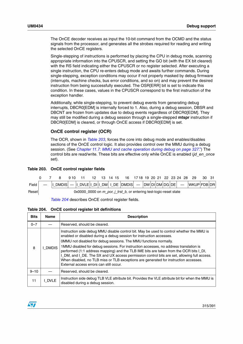
UM0434 Debug support
315/391
The OnCE decoder receives as input the 10-bit command from the OCMD and the status signals from the processor, and generates all the strobes required for reading and writing the selected OnCE registers.
Single-stepping of instructions is performed by placing the CPU in debug mode, scanning appropriate information into the CPUSCR, and setting the GO bit (with the EX bit cleared) with the RS field indicating either the CPUSCR or no register selected. After executing a single instruction, the CPU re-enters debug mode and awaits further commands. During single-stepping, exception conditions may occur if not properly masked by debug firmware (interrupts, machine checks, bus error conditions, and so on) and may prevent the desired instruction from being successfully executed. The OSR[ERR] bit is set to indicate this condition. In these cases, values in the CPUSCR correspond to the first instruction of the exception handler.
Additionally, while single-stepping, to prevent debug events from generating debug interrupts, DBCR0[EDM] is internally forced to 1. Also, during a debug session, DBSR and DBCNT are frozen from updates due to debug events regardless of DBCR0[EDM]. They may still be modified during a debug session through a single-stepped mtspr instruction if DBCR0[EDM] is cleared, or through OnCE access if DBCR0[EDM] is set.
OnCE control register (OCR)
The OCR, shown in Table 203, forces the core into debug mode and enables/disables sections of the OnCE control logic. It also provides control over the MMU during a debug session. (See Chapter 11.7: MMU and cache operation during debug on page 327.”) The control bits are read/write. These bits are effective only while OnCE is enabled (jd_en_once set).
Table 204 describes OnCE control register fields.
Table 203. OnCE control register fields
0 7 8 9 10 11 12 13 14 15 16 17 18 19 20 21 22 23 24 28 29 30 31
Field — I_DMDIS — I_DVLE I_DI I_DM I_DE DMDIS — DW DI DM DG DE — WKUP FDB DR
Reset 0x0000_0000 on m_por, j_trst_b, or entering test-logic-reset state
Table 204. OnCE control register bit definitions
Bits Name Description
0–7 — Reserved, should be cleared.
8 I_DMDIS
Instruction side debug MMU disable control bit. May be used to control whether the MMU is enabled or disabled during a debug session for instruction accesses.
0MMU not disabled for debug sessions. The MMU functions normally.
1MMU disabled for debug sessions. For instruction accesses, no address translation is performed (1:1 address mapping) and the TLB IME bits are taken from the OCR bits I_DI, I_DM, and I_DE. The SX and UX access permission control bits are set, allowing full access. When disabled, no TLB miss or TLB exceptions are generated for instruction accesses. External access errors can still occur.
9–10 — Reserved, should be cleared.
11 I_DVLEInstruction side debug TLB VLE attribute bit. Provides the VLE attribute bit for when the MMU is disabled during a debug session.

Debug support UM0434
316/391
12 I_DIInstruction side debug TLB I attribute bit. Provides the I attribute bit for instruction accesses when the MMU is disabled for instruction accesses during a debug session.
13 I_DMInstruction side debug TLB M attribute bit. Provides the M attribute bit to be used for instruction accesses when the MMU is disabled for instruction accesses during a debug session.
14 — Reserved, should be cleared.
15 I_DEInstruction side debug TLB E attribute bit. Provides the E attribute bit for instruction accesses when the MMU is disabled for instruction accesses during a debug session.
16 D_DMDIS
Data side debug MMU disable control bit. Controls whether the MMU is enabled normally or is disabled during a debug session for data accesses.
0 MMU not disabled for debug sessions. The MMU functions normally1 MMU disabled for debug sessions. For data accesses, no address translation is performed (1:1 address mapping) and the TLB WIMGE bits are taken from the OCR bits D_DW, D_DI, D_DM, D_DG, and D_DE bits. The SR, SW, UR, and UW access permission control bits are set to allow full access. When disabled, no TLB miss or TLB exceptions are generated for data accesses. External access errors can still occur.
17–18 — Reserved, should be cleared.
19 D_DWData side debug TLB W attribute bit. Provides the W attribute bit for data accesses when the MMU is disabled for data accesses during a debug session.
20 D_DIData side debug TLB I attribute bit. Provides the I attribute bit for data accesses when the MMU is disabled for data accesses during a debug session.
21 D_DMData side debug TLB M attribute bit. Provides the M attribute bit for data accesses when the MMU is disabled for data accesses during a debug session.
22 D_DGData side debug TLB G attribute bit. Provides the G attribute bit for data accesses when the MMU is disabled for data accesses during a debug session.
23 D_DEData side debug TLB E attribute bit. Provides the E attribute bit for data accesses when the MMU is disabled for data accesses during a debug session.
24–28 — Reserved, should be cleared.
29 WKUP
Wakeup request bit. Used to force the p_wakeup output to be asserted. To ensure that debug resources may be properly accessed by external hardware through scan sequences, debug firmware can use this control function to request that the chip-level clock controller restore the m_clk input to normal operation regardless of whether the core is in a low-power state.
30 FDB
Force breakpoint debug mode. Determines whether the processor is operating in breakpoint debug enable mode. The processor may be placed in breakpoint debug enable mode by setting this bit. In breakpoint debug enable mode, execution of the bkpt pseudo-instruction causes the processor to enter debug mode, as if the jd_de_b input had been asserted. FDB is qualified with DBCR0[EDM], which must be set for FDB to take effect.
31 DR
CPU debug request control. Used to unconditionally request the CPU to enter debug mode. The CPU indicates that debug mode has been entered via the data scanned out in the shift-IR state.
0 No debug mode request1 Unconditional debug mode request. The processor enters debug mode at the next instruction boundary.
Table 204. OnCE control register bit definitions (continued)
Bits Name Description

UM0434 Debug support
317/391
11.5.6 Access to debug resources
Resources contained in the OnCE module that do not require the core to be halted for access may be accessed without interfering with processor execution. Accesses to other resources such as the CPUSCR require the core to be placed in debug mode to avoid synchronization hazards. Debug firmware may ensure that it is safe to access these resources by determining the state of the core before access.
Note: A scan operation to update the CPUSCR is required before exiting debug mode.
Some cases of write accesses other than accesses to the OnCE command and control registers or DBCR0[EDM] require the m_clk to be running for proper operation. The OnCE control register provides a means of signaling this need to a system level clock control module.
In addition, because the CPU may cause multiple bits of certain registers to change state, reads of certain registers while the CPU is running (for example, DBSR and DBCNT) may not have consistent bit settings unless read twice with the same value indicated. To guarantee that the contents are consistent, the CPU should be placed into debug mode, or multiple reads should be performed until consistent values have been obtained on consecutive reads.
Table 205 lists access requirements for OnCE registers.
Table 205. OnCE register access requirements
Register name
Access requirements
Notes jd_en_once
to be Set
DBCR0
[EDM] = 1
m_clk active
for Write
Access
CPU to be
Halted
for Read Access
CPU to be
Halted
for Write
Access
Enable_OnCE N N N N —
Bypass N N N N N
CPUSCR Y Y Y Y Y
DAC1 Y Y Y N *(1)
DAC2 Y Y Y N *(1)
DBCNT Y Y Y N *(1)
Date read from DBCNT while the CPU is running may not be self-consistent due to synchronization across clock domains.
DBCR0 Y Y Y N *(1) *DBCR0[EDM] access only requires jd_en_once set
DBCR1 Y Y Y N *(1)
DBCR2 Y Y Y N *(1)
DBCR3 Y Y Y N *(1)

Debug support UM0434
318/391
11.5.7 Methods for entering debug mode
The OSR indicates that the CPU has entered the debug mode through the debug status bit. The following sections describe how debug mode is entered assuming the OnCE circuitry has been enabled. OnCE operation is enabled by the assertion of the jd_en_once input (see Table 195).
DBSR Y Y Y N *(1)
Reads of DBSR while the CPU is running may not give data that is self-consistent due to synchronization across clock domains.
IAC1 Y Y Y N *(1)
IAC2 Y Y Y N *(1)
IAC3 Y Y Y N *(1)
IAC4 Y Y Y N *(1)
JTAG ID N N — N — Read only
OCR Y N N N N
OSR Y N — N —Read only, accessed by scanning out IR while jd_en_once is set
PC FIFO Y N — N —
Read only, updates frozen while OCMD holds PCFIFO register encoding
Note: PCFIFO cannot be updated while the OnCE state machine is in Test_Logic_Reset state
Cache debug access control (CDACNTL)
Y N Y Y YCPU must be in debug mode with clocks running
Cache debug access data
(CDADATA)Y N Y Y Y
CPU must be in debug mode with clocks running
Nexus3-Access Y N N N N
External GPRs Y N N N N
LSRL Select Y N ? ? ?System test logic implementation determines LSRL functionality
1. Writes to these registers while the CPU is running may have unpredictable results due to the pipelined nature of the operation and the fact that updates are not synchronized to a particular clock, instruction, or bus cycle boundary; therefore, it is strongly recommended to ensure the processor is first placed into debug mode before updates to these registers are performed.
Table 205. OnCE register access requirements (continued)
Register name
Access requirements
Notes jd_en_once
to be Set
DBCR0
[EDM] = 1
m_clk active
for Write
Access
CPU to be
Halted
for Read Access
CPU to be
Halted
for Write
Access

UM0434 Debug support
319/391
Table 206 describes the methods for entering debug mode.
11.5.8 CPU status and control scan chain register (CPUSCR)
A number of on-chip registers store the CPU pipeline status and are configured in a single scan chain for access by the OnCE controller. CPUSCR contains these processor resources, which are used to restore the pipeline and resume normal chip activity upon return from debug mode, as well as a mechanism for the emulator software to access
Table 206. Methods for entering debug mode
Method name
Description
External debug request during reset
Holding jd_de_b asserted while p_reset_b is asserted and holding it asserted following the negation of p_reset_b causes the core to enter debug mode. After receiving an acknowledge through the OnCE status register debug bit, the external command controller should negate jd_de_b before sending the first command. Note that in this case the core does not execute an instruction before entering debug mode, although the first instruction to be executed may be fetched before entering debug mode.
In this case, all values in the debug scan chain are undefined and the external debug control module is responsible for proper initialization of the chain before debug mode is exited. In particular, the exception processing associated with reset may not be performed when debug mode is exited; thus, the debug controller must initialize PC, MSR, and IR to the image that the processor would have obtained in performing reset exception processing, or it must cause the appropriate bit reset to be re-asserted.
Debug request during reset
Setting OCR[DR] while p_reset_b is asserted causes the device to enter debug mode; the chip may fetch the first instruction of the reset interrupt handler but does not execute an instruction before entering debug mode. In this case, all values in the debug scan chain are undefined and the external debug control module is responsible for properly initializing the chain before debug mode is exited. In particular, interrupt processing associated with reset may not be performed when debug mode is exited; thus, the debug controller must initialize PC, MSR, and IR to the image that the processor would have obtained in performing reset exception processing, or it must cause the appropriate reset to be re-asserted.
Debug request during normal activity
Setting OCR[DR] during normal chip activity causes the chip to finish execution of the current instruction and then enter debug mode. Note that in this case the chip completes execution of the current instruction and stops after the newly fetched instruction enters the CPU instruction register. This process is the same for any newly fetched instruction, including instructions fetched by the interrupt processing or those aborted by the interrupt processing.
Debug request during halted or stopped state
Setting OCR[DR] when the device is in the halted or stopped state (p_halted or p_stopped set) causes the CPU to exit the state and enter debug mode once the CPU clock m_clk has been restored. Note that in this case, the CPU negates both the p_halted and p_stopped outputs. Once the debug session has ended, the CPU returns to the state it was in before entering debug mode. To signal the chip-level clock generator to re-enable m_clk, the p_wakeup output is set whenever the debug block is asserting a debug request to the CPU due to OCR[DR] being set, or jd_de_b assertion, and remains set from then until the debug session ends (jd_debug_b goes from set to negated). In addition, the status of the jd_mclk_on input (after synchronization to the j_tclk clock domain) may be sampled along with other status bits from the j_tdo output during the Shift-IR TAP controller state. This status may be used if necessary by external debug firmware to ensure that proper scan sequences occur to registers in the m_clk clock domain.
Software request during normal activity
Upon executing a ‘bkpt’ pseudo-instruction (for the core, defined to be an all zeros instruction opcode), when OCR [FDB] is set (debug mode enable control bit is true) and DBCR0[EDM] = 1, the CPU enters debug mode after the instruction following the ‘bkpt’ pseudo-instruction has entered the instruction register.

Debug support UM0434
320/391
processor and memory contents. Figure 70 shows the block diagram of the pipeline information registers contained in the CPUSCR. Once debug mode has been entered, it is required to scan in and update this register before exiting debug mode.
Figure 70. CPU scan chain register (CPUSCR)
Instruction register (IR)
The instruction register provides a way to control the debug session by serving as a means of forcing in selected instructions and causing them to be executed in a controlled manner by the debug control block. The opcode of the next instruction to be executed when entering debug mode is contained in this register when the scan-out of this chain begins. This value should be saved for later restoration if continuation of the normal instruction stream is desired.
On scan-in, in preparation for exiting debug mode, this register is filled with an instruction opcode selected by debug control software. By selecting appropriate instructions and controlling the execution of those instructions, the results of execution may be used to examine or change memory locations and processor registers. The debug control module external to the processor core controls execution by providing a single-step capability. Once the debug session is complete and normal processing is to be resumed, this register may be loaded with the value originally scanned out.
TDO
TDI
TCK
MSR
WBBRUpper
32
320 31
0 31
PC
320 31
IR
320 31
CTL
320 31
WBBRLower
320 31

UM0434 Debug support
321/391
Control state register (CTL)
The control state register (CTL), shown in Table 207, stores the value of certain internal CPU state variables before debug mode is entered. This register is affected by the operations performed during the debug session and should normally be restored by the external command controller when returning to normal mode. In addition to saved internal state variables, two of the bits are used by emulation firmware to control the debug process. In certain circumstances, emulation firmware must modify the content of this register as well as the PC and IR values in the CPUSCR before exiting debug mode. These cases are described more specifically in the text after the table.
Table 207. Control state register (CTL)
0 15
Field Internal state bits
16 19 20 21 22 23 24 25 26 27 28 29 30 31
Field PCOFSTPCINVFFRAIRSTAT
0IRSTAT
1IRSTAT
2IRSTAT
3IRSTAT
4IRSTAT
5IRSTAT
6IRSTAT
7IRSTAT
8IRSTAT
9
Table 208. CTL field definitions
Bits Name Description
0–15Internal
state bits
Internal state bits.These control bits represent the internal processor state and should be restored to their original value after a debug session is completed, that is, when a OnCE command is issued with the GO and EX bits set and not ignored. When performing instruction execution during a debug session (see Chapter 11.2.1: Software debug facilities on page 296”), these bits should be cleared.
16–19 PCOFST
PC offset field. Indicates whether the value in the PC portion of the CPUSCR must be adjusted before exiting debug mode. Due to the pipelined nature of the CPU, the PC value must be backed up by emulation software in certain circumstances. The PCOFST field specifies the value to be subtracted from the original value of the PC. This adjusted PC value should be restored into the PC portion of the CPUSCR just before exiting debug mode with a Go+Exit. In the event the PCOFST is non-zero, the IR should be loaded with a nop instruction instead of the original IR value; otherwise, the original value of IR should be restored (but see PCINV which overrides this field).
0000 No correction required0001 Subtract 0x04 from PC.
0010 Subtract 0x08 from PC.
0011 Subtract 0x0C from PC.0100 Subtract 0x10 from PC.
0101 Subtract 0x14 from PC.
All other encodings are reserved.
20 PCINV
PC and IR invalid status bit. This status bit indicates that the values in the IR and PC portions of the CPUSCR are invalid. Exiting debug mode with the saved values in the PC and IR will have unpredictable results. Debug firmware should initialize the PC and IR values in the CPUSCR with desired values before exiting debug mode if this bit was set when debug mode was initially entered.
0 No error condition exists.
1 Error condition exists. PC and IR are corrupted.

Debug support UM0434
322/391
Emulation firmware should modify the CTL, PC, and IR values in the CPUSCR during execution of debug-related instructions as well as just before exiting debug with a Go+Exit
21 FFRA
Feed forward RA operand bit. This control bit causes the content of the WBBRlower to be used as the rA (rS for logical and shift operations) operand value of the first instruction to be executed following an update of the CPUSCR. This allows the debug firmware to update processor registers, initialize the WBBRlower with the desired value, set the FFRA bit, and execute an ori Rx,Rx,0 instruction to the desired register.0 No action
1 Content of WBBR used as rA (rS for logical and shift operations) operand value
22 IRSTAT0
IR status bit 0.This control bit indicates an ERROR termination status for the IR.
0 No TEA occurred on the fetch of this instruction.
1 A TEA occurred on the fetch of this instruction
23 IRSTAT1
IR status bit 1. Indicates a TLB miss status for the IR.
0 No TLB miss occurred on the fetch of this instruction.1 TLB miss occurred on the fetch of this instruction.
24 IRSTAT2
IR status bit 2. Indicates an instruction address compare 1 event status for the IR.
0 No instruction address compare 1 event occurred on the fetch of this instruction.1 An instruction address compare 1 event occurred on the fetch of this instruction.
25 IRSTAT3IR status bit 3. Indicates an instruction address compare 2 event status for the IR. 0 No instruction address compare 2 event occurred on the fetch of this instruction.
1 An instruction address compare 2 event occurred on the fetch of this instruction.
26 IRSTAT4
IR status bit 4. Indicates an instruction address compare 3 event status for the IR.
0 No instruction address compare 3 event occurred on the fetch of this instruction.
1 An instruction address compare 3 event occurred on the fetch of this instruction.
27 IRSTAT5
IR status bit 5. Indicates an instruction address compare 4 event status for the IR.
0 No instruction address compare 4 event occurred on the fetch of this instruction.1 An instruction address compare 4 event occurred on the fetch of this instruction.
28 IRSTAT6IR status bit 6. This control bit indicates a parity error status for the IR. 0 No parity error occurred on the fetch of this instruction.
1 A parity error occurred on the fetch of this instruction.
29 IRSTAT7
IR status bit 7. Indicates a precise external termination error status for the IR.
0 No precise external termination error occurred on the fetch of this instruction.
1 Precise external termination error occurred on the fetch of this instruction.
30 IRSTAT8
IR status bit 8. Indicates the VLE status for the IR. IRStat8 affects the behavior of IRStat9.
0 IR contains a BookE instruction.1 IR contains a VLE instruction, aligned in the most significant portion of IR if 16-bit.
31 IRSTAT9
IR status bit 9. Indicates the VLE byte-ordering error status for the IR or a Book E misaligned instruction fetch, depending on the state of IRStat8.
0 IR contains an instruction without a byte-ordering error and no misaligned instruction fetch exception has occurred (no MIF).
1 If IRStat8 = 0, A Book E misaligned instruction fetch exception occurred while filling the IR. If IRStat8 = 1, IR contains an instruction with a byte-ordering error due to mismatched VLE
page attributes, or due to E indicating little-endian for a VLE page.
Table 208. CTL field definitions (continued)
Bits Name Description
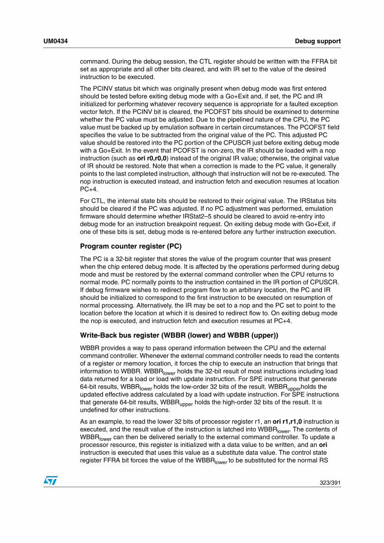
UM0434 Debug support
323/391
command. During the debug session, the CTL register should be written with the FFRA bit set as appropriate and all other bits cleared, and with IR set to the value of the desired instruction to be executed.
The PCINV status bit which was originally present when debug mode was first entered should be tested before exiting debug mode with a Go+Exit and, if set, the PC and IR initialized for performing whatever recovery sequence is appropriate for a faulted exception vector fetch. If the PCINV bit is cleared, the PCOFST bits should be examined to determine whether the PC value must be adjusted. Due to the pipelined nature of the CPU, the PC value must be backed up by emulation software in certain circumstances. The PCOFST field specifies the value to be subtracted from the original value of the PC. This adjusted PC value should be restored into the PC portion of the CPUSCR just before exiting debug mode with a Go+Exit. In the event that PCOFST is non-zero, the IR should be loaded with a nop instruction (such as ori r0,r0,0) instead of the original IR value; otherwise, the original value of IR should be restored. Note that when a correction is made to the PC value, it generally points to the last completed instruction, although that instruction will not be re-executed. The nop instruction is executed instead, and instruction fetch and execution resumes at location PC+4.
For CTL, the internal state bits should be restored to their original value. The IRStatus bits should be cleared if the PC was adjusted. If no PC adjustment was performed, emulation firmware should determine whether IRStat2–5 should be cleared to avoid re-entry into debug mode for an instruction breakpoint request. On exiting debug mode with Go+Exit, if one of these bits is set, debug mode is re-entered before any further instruction execution.
Program counter register (PC)
The PC is a 32-bit register that stores the value of the program counter that was present when the chip entered debug mode. It is affected by the operations performed during debug mode and must be restored by the external command controller when the CPU returns to normal mode. PC normally points to the instruction contained in the IR portion of CPUSCR. If debug firmware wishes to redirect program flow to an arbitrary location, the PC and IR should be initialized to correspond to the first instruction to be executed on resumption of normal processing. Alternatively, the IR may be set to a nop and the PC set to point to the location before the location at which it is desired to redirect flow to. On exiting debug mode the nop is executed, and instruction fetch and execution resumes at PC+4.
Write-Back bus register (WBBR (lower) and WBBR (upper))
WBBR provides a way to pass operand information between the CPU and the external command controller. Whenever the external command controller needs to read the contents of a register or memory location, it forces the chip to execute an instruction that brings that information to WBBR. WBBRlower holds the 32-bit result of most instructions including load data returned for a load or load with update instruction. For SPE instructions that generate 64-bit results, WBBRlower holds the low-order 32 bits of the result. WBBRupperholds the updated effective address calculated by a load with update instruction. For SPE instructions that generate 64-bit results, WBBRupper holds the high-order 32 bits of the result. It is undefined for other instructions.
As an example, to read the lower 32 bits of processor register r1, an ori r1,r1,0 instruction is executed, and the result value of the instruction is latched into WBBRlower. The contents of WBBRlower can then be delivered serially to the external command controller. To update a processor resource, this register is initialized with a data value to be written, and an ori instruction is executed that uses this value as a substitute data value. The control state register FFRA bit forces the value of the WBBRlower to be substituted for the normal RS

Debug support UM0434
324/391
source value of the ori instruction, thus allowing updates to processor registers to be performed. (Refer to Chapter : Control state register (CTL) on page 321,” for more details.).
WBBRlower and WBBRupper are generally undefined on instructions that do not write back a result and, due to control issues, are not defined on lmw or branch instructions either.
To read and write the entire 64 bits of a GPR, both WBBRlower and WBBRupper are used. For reads, an evslwi rn,rn,0 may be used. For writes, the same instruction may be used, but the CTL[FFRA] bit must be set as well.
Note: MSR[SPE] must be set in order for these operations to be performed properly.
Machine state register (MSR)
The MSR is a 32-bit register used to read/write the machine state register (MSR). Whenever the external command controller needs to save or modify the contents of the machine state register, this register is used. This register is affected by the operations performed during debug mode and must be restored by the external command controller when returning to normal mode. Chapter 4: Register model on page 38,” further describes the MSR.
11.5.9 Instruction address FIFO buffer (PC FIFO)
To assist debugging and keep track of program flow, a first-in-first-out (FIFO) buffer stores the addresses of the last eight instruction change-of-flow destinations that were fetched. These include exception vectoring to an exception handler and returns, as well as pipeline refills due to execution of the isync instruction.
The PC FIFO stores the addresses of the last eight instruction change-of-flow addresses that were actually taken. The FIFO is implemented as a circular buffer containing eight 32-bit registers and one 3-bit counter. All the registers have the same address, but any read access to the FIFO address causes the counter to increment, making it point to the next FIFO register. The registers are serially available to the external command controller through the common FIFO address. Figure 71 shows the block diagram of the PC FIFO.

UM0434 Debug support
325/391
Figure 71. OnCE PC FIFO
The FIFO is not affected by the operations performed during a debug session except for the FIFO pointer increment when reading the FIFO. When entering debug mode, the FIFO counter is pointing to the FIFO register containing the address of the oldest of the eight change-of-flow prefetches. When OCMD [RS] is loaded with the value corresponding to the PC FIFO (010 1101), the current pointer value is captured into a temporary register. This temporary value (not the actual FIFO counter) is incremented as FIFO reads are performed. The first FIFO read obtains the oldest address and the following FIFO read returns the other addresses from the oldest to the newest (the order of execution).
Updates to the FIFO are frozen whenever the OCMD register contains a command whose RS[0–6] field points to the PC FIFO (010 1101) to allow firmware to read the contents of the PC FIFO without placing the CPU into debug mode. After completing all accesses to the PC
PC FIFO Register 0
TDOTCK
PC FIFO Register 1
PC FIFO Register 2
PC FIFO Register 3
PC FIFO Register 4
Instruction Fetch Address
CircularBufferPointer
PC FIFO Shift Register
PC FIFO Register 5
PC FIFO Register 6
PC FIFO Register 7

Debug support UM0434
326/391
FIFO, another OCMD value that does not select the PC FIFO should be entered to allow the PC FIFO to resume updating.
To ensure FIFO coherence, a complete set of eight reads of the FIFO should be performed because each read increments the temporary FIFO pointer, thus making it point to the next location. After eight reads the pointer points to the same location it pointed to before starting the read procedure. The temporary counter value captures the actual counter each time the OCMD RS field transitions to the value corresponding to the PC FIFO (010 1101).
The FIFO pointer is reset to entry 0 when either j_trst_b or m_por is set.
11.5.10 Reserved registers
The reserved registers are used to control various test control logic. These registers are not intended for customer use. To preclude device and/or system damage, these registers should not be accessed.
11.6 Watchpoint supportThe core supports the generation and signaling of watchpoints when operating in internal debug mode (DBCR0[IDM] = 1) or in external debug mode (DBCR0[EDM] = 1). Watchpoints are indicated with a dedicated set of interface signals. The jd_watchpoint[0:7] output signals are used to indicate that a watchpoint has occurred.
Each debug address compare function (IAC1–IAC4, DAC1 and DAC2) and debug counter event (DCNT1 and DCNT2) can trigger a watchpoint output. The DBCR1, DBCR2, and DBCR3 control fields are used to configure watchpoints, regardless of whether events are enabled in DBCR0. Watchpoints may occur whenever an associated event would have been posted in the debug status register if enabled. No explicit enable bits are provided for watchpoints; they are always enabled by definition (except during a debug session). If not desired, the base address values for these events may be programmed to an unused system address. MSR[DE] has no effect on watchpoint generation.
External logic may monitor the assertion of these signals for debugging purposes. Watchpoints are signaled in the clock cycle following the occurrence of the actual event. The Nexus3 module also monitors assertion of these signals for various development control purposes.
Table 209. Watchpoint output signal assignments
Signal name Type Description
jd_watchpt[0] IAC1Instruction address compare 1 watchpoint. Set whenever an IAC1 compare occurs regardless of whether IAC1 compares are enabled to set DBSR status.
jd_watchpt[1] IAC2Instruction address compare 2 watchpoint. Set whenever an IAC2 compare occurs regardless of whether IAC2 compares are enabled to set DBSR status.
jd_watchpt[2] IAC3Instruction address compare 3 watchpoint. Set whenever an IAC3 compare occurs regardless of whether IAC3 compares are enabled to set DBSR status.
jd_watchpt[3] IAC4Instruction address compare 4 watchpoint. Set whenever an IAC4 compare occurs regardless of whether IAC4 compares are enabled to set DBSR status.

UM0434 Debug support
327/391
11.7 MMU and cache operation during debugNormal operation of the MMU may be modified during a debug session using the OnCE OCR. A debug session begins when the CPU initially enters debug mode and ends when a OnCE command with Go+Exit is executed, releasing the CPU for normal operation. If desired during a debug session, the debug firmware may disable the translation process and may substitute default values for the access protection (UX, UR, UW, SX, SR, SW) bits, and values obtained from the OnCE control register and page attribute (VLE, W, I, M, G, E) bits normally provided by a matching TLB entry. In addition, no address translation is performed; instead, a 1:1 mapping of effective-to-real addresses is performed.
When disabled during a debug session, TLB miss or TLB-related DSI conditions cannot occur. If the debugger desires to use the normal translation process, the MMU may be left enabled in the OnCE OCR, and normal translation (including the possibility of a TLB miss or DSI) remains in effect.
The OCRDMDIS, DW, DI, DM, DG, and DE control bits are used when debug mode is entered. Refer to the bit definitions in the OCR (See Chapter : OnCE control register (OCR) on page 315,” for more detail). These substituted page attribute bits control cache operation on accesses initiated during debug. No address translation is performed; instead, a 1:1 mapping between effective and real addresses is performed.
11.8 Enabling, using, and exiting external debug Mode: exampleThe following steps show one possible scenario for a debugger wishing to use the external debug facilities. This simplified flow shows basic operations and does not cover all potential methods in depth.
Enable external debug mode and initialize debug registers:
1. To enable OnCE operation, the debugger should ensure that the jd_en_once is set.
2. Write a value to OCR in which OCR[DR] and OCR[WKUP] are set. The TAP controller must step through the proper states as outlined earlier. This step places the CPU in a
jd_watchpt[4] DAC1(1)Data address compare 1 watchpoint. Set whenever a DAC1 compare occurs regardless of whether DAC1 compares are enabled to set DBSR status.
jd_watchpt[5] DAC2(1)Data address compare 2 watchpoint. Set whenever a DAC2 compare occurs regardless of whether DAC2 compares are enabled to set DBSR status.
jd_watchpt[6] DCNT1Debug counter 1 watchpoint. Set whenever debug counter 1 decrements to zero regardless of whether DCNT1 compares are enabled to set DBSR status.
jd_watchpt[7] DCNT2Debug counter 2 watchpoint. Set whenever debug counter 2 decrements to zero regardless of whether DCNT2 compares are enabled to set DBSR status.
1. If the corresponding event is completely disabled in DBCR0, either load-type or store-type data accesses are allowed to generate watchpoints, otherwise watchpoints are generated only for the enabled conditions.
Table 209. Watchpoint output signal assignments (continued)
Signal name Type Description

Debug support UM0434
328/391
debug state where it is halted and awaiting single-step commands or a release to normal mode.
3. Scan out the OSR value to determine that the CPU clock is running and the CPU has entered debug state. This can be done in conjunction with a CPUSCR read. The OSR is shifted out during the Shift-IR state. The CPUSCR is shifted out during the Shift-DR state. The debugger should save the scanned-out value of CPUSCR for later restoration.
4. Select the DBCR0 register and update it with DBCR0[EDM] set.
5. Clear the DBSR status bits.
6. Write appropriate values to the DBCR0–DBCR3, IAC, DAC, and DBCNT registers.
Note: The initial write to DBCR0 only affects the EDM bit, so the remaining portion of the register must now be initialized, keeping the EDM bit set.
At this point the system is ready to begin debug operations. Depending on the desired operation, different steps must occur.
1. Optionally set the OCR[DMDIS] control bit to ensure that no TLB misses occur while performing the debug operations.
2. Optionally ensure that the values entered into the MSR portion of the CPUSCR during the following steps cause interrupts to be disabled (clearing MSR[EE] and MSR[CE]). This ensures that external interrupt sources do not cause single-step errors.
To single-step the CPU:
1. The debugger scans in either a new or a previously saved value of the CPUSCR (with appropriate modification of the PC and IR as described in Chapter : Control state register (CTL) on page 321”) with a Go+NoExit OnCE command value.
2. The debugger scans out the OSR with no register selected, GO cleared, and determines that the PCU has re-entered the debug state and that no ERR condition occurred.
To return the CPU to normal operation (without disabling external debug mode):
1. OCR[DMDIS] and OCR[DR] should be cleared, leaving OCR[WKUP] set.
2. The debugger restores the CPUSCR with a previously saved value of the CPUSCR (with appropriate modification of the PC and IR as described in Chapter : Control state register (CTL) on page 321”), with a Go+Exit OnCE command value.
3. OCR[WKUP] may then be cleared.
To exit external debug mode:
1. The debugger should place the CPU in the debug state through the OCR[DR] with OCR[WKUP] set, scanning out and saving the CPUSCR.
2. The debugger should write to DBCR0–DBCR3 as needed, likely clearing every enable except DBCR0[EDM].
3. The debugger should write the DBSR to a cleared state.
4. The debugger should rewrite the DBCR0 with all bits including EDM cleared.
5. The debugger should clear OCR[DR].
6. The debugger restores the CPUSCR with the previously saved value of the CPUSCR (with appropriate modification of the PC and IR as described in Chapter : Control state register (CTL) on page 321”) with a Go+Exit OnCE command value.
7. OCR[WKUP] may then be cleared.
Note: These steps are only examples rather than an exact template for debugger operations.

UM0434 Nexus3 module
329/391
12 Nexus3 module
The e200z3 Nexus3 module provides real-time development capabilities for e200z3 processors in compliance with the IEEE-ISTO Nexus 5001-2003 standard. This module provides development support capabilities without requiring the use of address and data pins for internal visibility.
A portion of the pin interface (the JTAG port) is also shared with the OnCE/Nexus1 unit. The IEEE-ISTO 5001-2003 standard defines an extensible auxiliary port which is used in conjunction with the JTAG port in e200z3 processors.
12.1 Introduction
12.1.1 General description
This chapter defines the auxiliary pin functions, transfer protocols and standard development features of a class 3 device in compliance with the IEEE-ISTO Nexus 5001-2003 standard. The development features supported are program trace, data trace, watchpoint messaging, ownership trace, and read/write access through the JTAG interface. The Nexus3 module also supports two class 4 features: watchpoint triggering, and processor overrun control.
12.1.2 Terms and definitions
Table 210 contains a set of terms and definitions associated with the Nexus3 module.
Table 210. Terms and definitions
Term Description
IEEE-ISTO 5001Consortium and standard for real-time embedded system design. World Wide Web documentation at the Nexus 5001™ Forum website.
Auxiliary portRefers to Nexus auxiliary port. Used as auxiliary port to the IEEE 1149.1 JTAG interface.
Branch trace messaging (BTM)
Visibility of addresses for taken branches and exceptions, and the number of sequential instructions executed between each taken branch.
Data read message (DRM) External visibility of data reads to memory-mapped resources.
Data write message (DWM) External visibility of data writes to memory-mapped resources.
Data trace messaging (DTM)
External visibility of how data flows through the embedded system. This may include DRM and/or DWM.
JTAG compliant Device complying to IEEE 1149.1 JTAG standard.
JTAG IR and DR sequence
JTAG instruction register (IR) scan to load an opcode value for selecting a development register. The JTAG IR corresponds to the OnCE command register (OCMD). The selected development register is then accessed through a JTAG data register (DR) scan.

Nexus3 module UM0434
330/391
12.1.3 Feature list
The Nexus3 module is compliant with class 3 of the IEEE-ISTO 5001-2003 standard. The following features are implemented:
● Program trace through branch trace messaging (BTM). Displays program flow discontinuities, direct and indirect branches, and exceptions, allowing the development tool to interpolate what transpires between the discontinuities. Thus static code may be traced.
● Data trace by means of data write messaging (DWM) and data read messaging (DRM). DRM and DWM provide the capability for the development tool to trace reads and/or writes to selected internal memory resources.
● Ownership trace by means of ownership trace messaging (OTM). Facilitates ownership trace by providing visibility of which process ID or operating system task is activated. An ownership trace message is transmitted when a new process/task is activated, allowing the development tool to trace ownership flow.
● Run-time access to embedded processor registers and memory map through the JTAG port. This allows for enhanced download/upload capabilities.
● Watchpoint messaging through the auxiliary pins
● Watchpoint trigger enable of program and/or data trace messaging
● Auxiliary interface for higher data input/output:
– Configurable, min/max, message data out pins, nex_mdo[n:0]– One or two message start/end out pins, nex_mseo_b[1:0]– One read/write ready pin, nex_rdy_b– One watchpoint event pin, nex_evto_b– One event in pin, nex_evti_b– One message clock out (MCKO) pin
Nexus1The e200z3 (OnCE) debug module. This module integrated with each e200z3 processor provides all static, core-halted, debug functionality. This module complies with class 1 of the IEEE-ISTO 5001 standard.
Ownership trace message (OTM)
Visibility of process/function that is currently executing.
Public messagesMessages on the auxiliary pins for meeting common visibility and controllability requirements.
SOCSystem-on-a-chip (SOC) signifies all of the modules on a single die. This generally includes one or more processors with associated peripherals, interfaces, and memory modules.
StandardThe phrase “according to the standard” is used to indicate the IEEE-ISTO 5001 standard.
Transfer code (TCODE)Message header that identifies the number and/or size of packets to be transferred and how to interpret each of the packets.
WatchpointA data or instruction breakpoint that does not cause the processor to halt. Instead, a pin is used to signal that the condition occurred. A watchpoint message is also generated.
Table 210. Terms and definitions (continued)
Term Description

UM0434 Nexus3 module
331/391
● Registers for program trace, data trace, ownership trace, and watchpoint trigger
● All features controllable and configurable through the JTAG port
Note: Configuration of the message data out pins is controlled by the port control register at the SoC level in multiple Nexus implementations. For single Nexus implementations, this configuration is controlled by DC1 within the e200z3 Nexus3 module. In either implementation, full port mode (FPM—maximum number of MDO pins) or reduced port mode (RPM—minimum number of MDO pins) is supported. This setting should not be changed while the system is running. The configuration of the message start/end out pins, 1 or 2, is determined at the SOC integration level. This option is hard-wired based on SOC bandwidth requirements. Figure 72 shows the functional block diagram.
Figure 72. Nexus3 functional block diagram
nex_mseo0_b
nex_mcko
Cor
e V
irtua
l Bus
AH
B S
yste
m B
us
Nexus3 Block
Nexus1 Block (within core CPU)
nex_mdo[n:0]
j_tdo
j_tdi
j_tmsj_tclkj_trst_b
nex_evto_b
nex_rdy_b
nex_evti_b
nex_mseo1_b
N+1
nex_aux_req[1:0]
npc_aux_grant
2
Note: The nex_aux_req[1:0], npc_aux_grant and nex_aux_busy signals are used for inter-module
nex_aux_busy
communication in a multiple Nexus environment. They are not pins on the SoC.
ext_multi_nex_sel
Registers
DMA Registers
OnCE Debug
Breakpoint/Watchpoint
Control
MemoryControl
Control/StatustRegisters
InstructionSnoop
I/OLogic
DataSnoop
DMA(R/W)
MessageQueues

Nexus3 module UM0434
332/391
12.2 Enabling Nexus3 operationThe Nexus module is enabled by loading a single instruction, NEXUS3-Access, into the JTAG instruction register/OnCE OCMD register. For the e200z3 Nexus3 module, the OCMD value is 0b00_0111_1100. Once enabled, the module is ready to accept control input through the JTAG/OnCE pins.
The Nexus module is disabled when the JTAG state machine reaches the test-logic-reset state. This state can be reached by the assertion of the j_trst_b pin or by cycling through the state machine using the j_tms pin. The Nexus module can also be disabled if a power-on reset (POR) event occurs. If the Nexus3 module is disabled, no trace output is provided, and the module disables auxiliary port output pins, nex_mdo[n:0], nex_mseo[1:0], and nex_mcko. Nexus registers are not available for reads or writes.
Note: See Nexus 3 Integration Guide for details on IEEE-ISTO 5001 compliance output pins & multiple Nexus module configurations.
12.3 TCODEs supportedThe Nexus3 pins allow for flexible transfer operations through public messages. A TCODE defines the transfer format, the number and/or size of the packets to be transferred, and the purpose of each packet. The IEEE-ISTO 5001-2003 standard defines a set of public messages. The Nexus3 block supports the public TCODEs seen in Table 211. Each message contains multiple packets transmitted in the order shown in the table.
Table 211. Public TCODEs supported
Message nameMinimum
Packet Size (Bits)
Maximum Packet
Size (Bits)
Packet type
Packet description
Debug status
6 6 Fixed TCODE number = 0 (0x00)
4 4 FixedSource processor identifier (multiple Nexus configuration)
8 8 Fixed Debug status register (DS[31–24])
Ownership trace message
6 6 Fixed TCODE number = 2 (0x02)
4 4 FixedSource processor identifier (multiple Nexus configuration)
32 32 Fixed Task/process ID tag
Program trace–Direct branch message
6 6 Fixed TCODE number = 3 (0x03)
4 4 FixedSource processor identifier (multiple Nexus configuration)
1 8 VariableNumber of sequential instructions executed since last taken branch
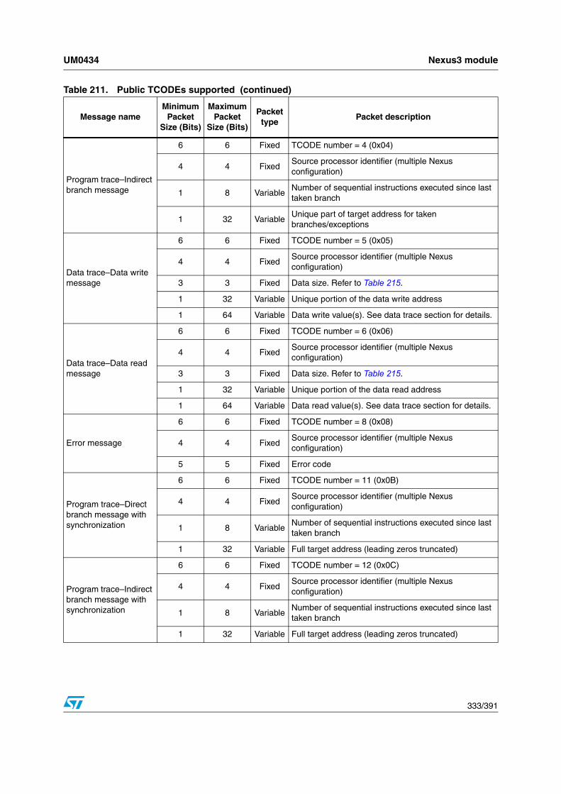
UM0434 Nexus3 module
333/391
Program trace–Indirect branch message
6 6 Fixed TCODE number = 4 (0x04)
4 4 FixedSource processor identifier (multiple Nexus configuration)
1 8 VariableNumber of sequential instructions executed since last taken branch
1 32 VariableUnique part of target address for taken branches/exceptions
Data trace–Data write message
6 6 Fixed TCODE number = 5 (0x05)
4 4 FixedSource processor identifier (multiple Nexus configuration)
3 3 Fixed Data size. Refer to Table 215.
1 32 Variable Unique portion of the data write address
1 64 Variable Data write value(s). See data trace section for details.
Data trace–Data read message
6 6 Fixed TCODE number = 6 (0x06)
4 4 FixedSource processor identifier (multiple Nexus configuration)
3 3 Fixed Data size. Refer to Table 215.
1 32 Variable Unique portion of the data read address
1 64 Variable Data read value(s). See data trace section for details.
Error message
6 6 Fixed TCODE number = 8 (0x08)
4 4 FixedSource processor identifier (multiple Nexus configuration)
5 5 Fixed Error code
Program trace–Direct branch message with synchronization
6 6 Fixed TCODE number = 11 (0x0B)
4 4 FixedSource processor identifier (multiple Nexus configuration)
1 8 VariableNumber of sequential instructions executed since last taken branch
1 32 Variable Full target address (leading zeros truncated)
Program trace–Indirect branch message with synchronization
6 6 Fixed TCODE number = 12 (0x0C)
4 4 FixedSource processor identifier (multiple Nexus configuration)
1 8 VariableNumber of sequential instructions executed since last taken branch
1 32 Variable Full target address (leading zeros truncated)
Table 211. Public TCODEs supported (continued)
Message nameMinimum
Packet Size (Bits)
Maximum Packet
Size (Bits)
Packet type
Packet description

Nexus3 module UM0434
334/391
Data trace–Data write message with synchronization
6 6 Fixed TCODE number = 13 (0x0D)
4 4 FixedSource processor identifier (multiple Nexus configuration)
3 3 Fixed Data size. Refer to Table 215.
1 32 Variable Full access address (leading zeros truncated)
1 64 Variable Data write value(s). See data trace section for details.
Data trace–Data read message with synchronization
6 6 Fixed TCODE number = 14 (0x0E)
4 4 FixedSource processor identifier (multiple Nexus configuration)
3 3 Fixed Data size. Refer to Table 215.
1 32 Variable Full access address (leading zeros truncated)
1 64 Variable Data read value(s). See data trace section for details.
Watchpoint message
6 6 Fixed TCODE number = 15 (0x0F)
4 4 FixedSource processor identifier (multiple Nexus configuration)
8 8 Fixed Number indicating watchpoint source(s)
Resource full message
6 6 Fixed TCODE number = 27 (0x1B)
4 4 FixedSource processor identifier (multiple Nexus configuration)
4 4 FixedResource code. Refer to Table 213. Indicates which resource is the cause of this message.
1 32 VariableBranch/predicate instruction history (see Chapter 12.7.1: Branch trace messaging (BTM) on page 350”)
Program trace–Indirect branch history message
6 6 Fixed TCODE number = 28 (0x1C). See note below.
4 4 FixedSource processor identifier (multiple Nexus configuration)
1 8 VariableNumber of sequential instructions executed since last taken branch
1 32 VariableUnique part of target address for taken branches/exceptions
1 32 VariableBranch/predicate instruction history (see Chapter 12.7.1: Branch trace messaging (BTM) on page 350”).
Table 211. Public TCODEs supported (continued)
Message nameMinimum
Packet Size (Bits)
Maximum Packet
Size (Bits)
Packet type
Packet description

UM0434 Nexus3 module
335/391
Table 212 shows error code encodings used when reporting an error through the Nexus3 error message.
Program trace–Indirect branch history message with synchronization
6 6 Fixed TCODE number = 29 (0x1D). See note below.
4 4 FixedSource processor identifier (multiple Nexus configuration)
1 8 VariableNumber of sequential instructions executed since last taken branch
1 32 Variable Full target address (leading zero (0) truncated)
1 32 VariableBranch/predicate instruction history (see Chapter 12.7.1: Branch trace messaging (BTM) on page 350”).
Program trace–Program correlation message
6 6 Fixed TCODE number = 33 (0x21)
4 4 FixedSource processor identifier (multiple Nexus configuration)
4 4 FixedEvent correlated with program flow. Refer to Table 214.
1 8 VariableNumber of sequential instructions executed since last taken branch
1 32 VariableBranch/predicate instruction history (see Chapter 12.7.1: Branch trace messaging (BTM) on page 350”).
Table 211. Public TCODEs supported (continued)
Message nameMinimum
Packet Size (Bits)
Maximum Packet
Size (Bits)
Packet type
Packet description
Table 212. Error code encodings (TCODE = 8)
Error code
(ECODE)Description
00000 Ownership trace overrun
00001 Program trace overrun
00010 Data trace overrun
00011 Read/write access error
00101 Invalid access opcode (Nexus register unimplemented)
00110 Watchpoint overrun
00111 Program trace or data trace and ownership trace overrun
01000 Program trace or data trace or ownership trace and watchpoint overrun
01001–10111 Reserved
11000 BTM lost due to collision with higher priority message
11001–11111 Reserved

Nexus3 module UM0434
336/391
Table 213 shows the encodings used for resource codes for certain messages.
Table 214 shows the event code encodings used for certain messages.
Table 215 shows the data trace size encodings used for certain messages.
Note: Program trace can be implemented using either branch history/predicate instruction messages, or traditional direct/indirect branch messages, and the user can select between the two types of program trace. The advantages of each are discussed in Chapter 12.7.1: Branch trace messaging (BTM) on page 350.” If the branch history method is selected, the shaded TCODES above will not be messaged out.
12.4 Nexus3 Programmer’s modelThis section describes the Nexus3 programmers model. Nexus3 registers are accessed using the JTAG/OnCE port in compliance with IEEE 1149.1. See Chapter 12.5: Nexus3 register access through JTAG/OnCE on page 348,” for details on Nexus3 register access.
Nexus3 registers and output signals are numbered using bit 0 as the least significant bit. This bit ordering is consistent with the ordering defined by the IEEE-ISTO 5001 standard.
Table 213. Resource code encodings (TCODE = 27)
Resource code
(RCODE)Description
0000 Program trace instruction counter reached 255 and was reset.
0001Program trace, branch/predicate instruction history. This type of packet is terminated by a stop bit set after the last history bit.
Table 214. Event code encodings (TCODE = 33)
Event code (EVCODE)
Description
0000 Entry into debug mode
0001 Entry into low power mode (CPU only)
0010–1111 Reserved
1110 Entry into a VLE page from a non-VLE page
1111 Entry into a non-VLE page from a VLE page
Table 215. Data trace size encodings (TCODE = 5, 6, 13, or 14)
DTM size encoding Transfer size
000 Byte
001 Half-word (2 bytes)
010 Word (4 bytes)
011 Double-word (8 bytes)
100 String (3 bytes)
101–111 Reserved

UM0434 Nexus3 module
337/391
Table 216 shows the register map for the Nexus3 module.
12.4.1 Client select control register (CSC)
The CSC register determines which Nexus client is under development. This register is present at the top-level SOC Nexus3 controller to select an on-chip Nexus3 units Table 217 shows the CSC register.
Table 216. Nexus3 register map
Nexus registerNexus access opcode
Read/WriteRead
addressWrite
address
Client select control (CSC)(1)
1. The CSC and PCR registers are shown in this table as part of the Nexus programmer’s model. They are only present at the top level SoC Nexus3 controller in a multiple Nexus implementation, not in the e200z3 Nexus3 module. The SoC’s CSC register is readable through Nexus3, but the PCR is shown here for reference only.
2 PCR_INDEX is a parameter determined by the SoC. Refer to the reference manual for the device integrating the e200z3 core for more information on how this parameter is implemented for each Nexus module.
0x1 R 0x02 —
Port configuration register (PCR)(1) PCR_INDEX2 R/W — —
Development control1 (DC1) 0x2 R/W 0x04 0x05
Development control2 (DC2) 0x3 R/W 0x06 0x07
Development status (DS) 0x4 R 0x08 —
Read/write access control/status (RWCS) 0x7 R/W 0x0E 0x0F
Read/write access address (RWA) 0x9 R/W 0x12 0x13
Read/write access data (RWD) 0xA R/W 0x14 0x15
Watchpoint trigger (WT) 0xB R/W 0x16 0x17
Data trace control (DTC) 0xD R/W 0x1A 0x1B
Data trace start address1 (DTSA1) 0xE R/W 0x1C 0x1D
Data trace start address2 (DTSA2) 0xF R/W 0x1E 0x1F
Data trace end address1 (DTEA1) 0x12 R/W 0x24 0x25
Data trace end address2 (DTEA2) 0x13 R/W 0x26 0x27
Reserved 0x14–0x3F — 0x28–0x7E 0x29–0x7F
Table 217. Client Select Control Register
7 4 3 0
Field — CS
Reset All zeros
R/W Read only
Number 0x1
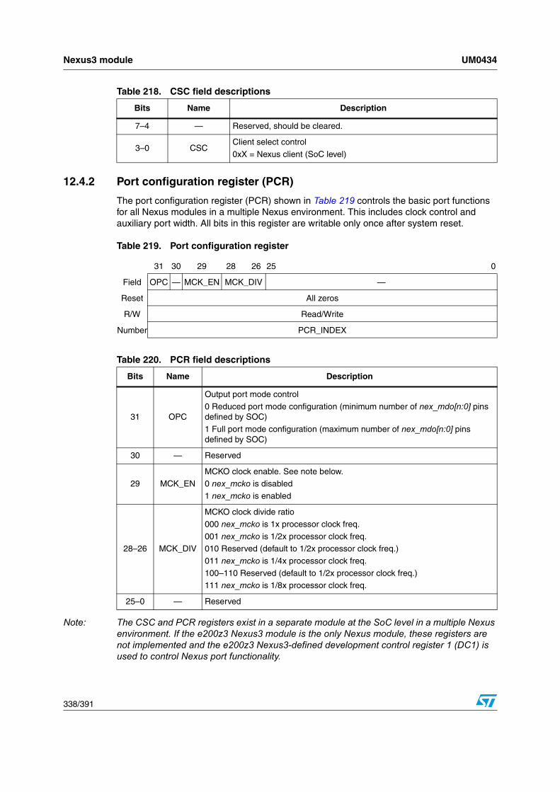
Nexus3 module UM0434
338/391
12.4.2 Port configuration register (PCR)
The port configuration register (PCR) shown in Table 219 controls the basic port functions for all Nexus modules in a multiple Nexus environment. This includes clock control and auxiliary port width. All bits in this register are writable only once after system reset.
Note: The CSC and PCR registers exist in a separate module at the SoC level in a multiple Nexus environment. If the e200z3 Nexus3 module is the only Nexus module, these registers are not implemented and the e200z3 Nexus3-defined development control register 1 (DC1) is used to control Nexus port functionality.
Table 218. CSC field descriptions
Bits Name Description
7–4 — Reserved, should be cleared.
3–0 CSCClient select control
0xX = Nexus client (SoC level)
Table 219. Port configuration register
31 30 29 28 26 25 0
Field OPC — MCK_EN MCK_DIV —
Reset All zeros
R/W Read/Write
Number PCR_INDEX
Table 220. PCR field descriptions
Bits Name Description
31 OPC
Output port mode control
0 Reduced port mode configuration (minimum number of nex_mdo[n:0] pins defined by SOC)
1 Full port mode configuration (maximum number of nex_mdo[n:0] pins defined by SOC)
30 — Reserved
29 MCK_ENMCKO clock enable. See note below.0 nex_mcko is disabled
1 nex_mcko is enabled
28–26 MCK_DIV
MCKO clock divide ratio
000 nex_mcko is 1x processor clock freq.
001 nex_mcko is 1/2x processor clock freq.010 Reserved (default to 1/2x processor clock freq.)
011 nex_mcko is 1/4x processor clock freq.
100–110 Reserved (default to 1/2x processor clock freq.)111 nex_mcko is 1/8x processor clock freq.
25–0 — Reserved

UM0434 Nexus3 module
339/391
12.4.3 Development control register 1, 2 (DC1, DC2)
The development control registers are used to control the basic development features of the Nexus3 module. Development control register 1 is shown in Table 221 and its fields are described in Table 219.
Table 221. Development control register 1 (DC1)
31 30 29 28 27 26 25 24 23 8 7 5 4 3 2 0
Field OPC MCK_DIV EOC — PTM WEN — OVC EIC TM
Reset All zeros
R/W Read/Write
Number 0x2
Table 222. DC1 field descriptions
Bits Name Description
31 OPC
Output port mode control
0 Reduced port mode configuration (minimum number of nex_mdo[n:0] pins defined by SOC)
1 Full port mode configuration (maximum number of nex_mdo[n:0] pins defined by SOC)
30–29 MCK_DIV
MCKO clock divide ratio. See note below.00 nex_mcko is 1x processor clock freq.
01 nex_mcko is 1/2x processor clock freq.
10 nex_mcko is 1/4x processor clock freq.11 nex_mcko is 1/8x processor clock freq.
28–27 EOC
EVTO control00 nex_evto_b upon occurrence of watchpoints (configured in DC2)
01 nex_evto_b upon entry into debug mode
10 nex_evto_b upon timestamping event11 Reserved
26 — Reserved
25 PTM
Program trace method
0 Program trace uses traditional branch messages.1 Program trace uses branch history messages.
24 WENWatchpoint trace enable0 Watchpoint messaging disabled
1 Watchpoint messaging enabled
23–8 — Reserved
7–5 OVC
Overrun control000 Generate overrun messages
001–010 Reserved
011 Delay processor for BTM/DTM/OTM overruns1XX Reserved

Nexus3 module UM0434
340/391
Note: OPC and MCK_DIV must be modified only during system reset or debug mode to ensure correct output port and output clock functionality. It is also recommended that all other bits of DC1 be modified only in one of these two modes.
Development control register 2 is shown in Table 223 and its fields are described in Table 224.
The EOC bits in DC1 must be programmed to trigger EVTO on watchpoint occurrence for the EWC bits to have any effect.
12.4.4 Development status register (DS)
The development status registe shown in Table 225 is used to report system debug status. When debug mode is entered or exited, or an SOC- or e200z3-defined low-power mode is
4–3 EIC
EVTI control
00nex_evti_b is used for synchronization (program trace/data trace)
01nex_evti_b is used for debug request1XReserved
2–0 TM
Trace mode000No trace
1XXProgram trace enabled
X1XData trace enabledXX1Ownership trace enabled
Table 222. DC1 field descriptions (continued)
Bits Name Description
Table 223. Development control register 2 (DC2)
31 24 23 0
Field EWC —
Reset All zeros
R/W Read/Write
Number 0x3
Table 224. DC2 field descriptions
Bits Name Description
31–24 EWC
EVTO Watchpoint Configuration
00000000No watchpoints trigger nex_evto_b1xxxxxxxWatchpoint #0 (IAC1 from Nexus1) triggers nex_evto_bx1xxxxxxWatchpoint #1 (IAC2 from Nexus1) triggers nex_evto_bxx1xxxxxWatchpoint #2 (IAC3 from Nexus1) triggers nex_evto_bxxx1xxxxWatchpoint #3 (IAC4 from Nexus1) triggers nex_evto_bxxxx1xxxWatchpoint #4 (DAC1 from Nexus1) triggers nex_evto_bxxxxx1xxWatchpoint #5 (DAC2 from Nexus1) triggers nex_evto_bxxxxxx1xWatchpoint #6 (DCNT1 from Nexus1) triggers nex_evto_bxxxxxxx1Watchpoint #7 (DCNT2 from Nexus1) triggers nex_evto_b
23–0 — Reserved

UM0434 Nexus3 module
341/391
entered, a debug status message is transmitted with DS[31–25]. The external tool can read this register at any time.
12.4.5 Read/Write access Control/Status register (RWCS)
The read write access control/status register, shown in Table 227, provides control for read/write access. Read/write access provides DMA-like access to memory-mapped resources on the AHB system bus either while the processor is halted, or during runtime. RWCS also provides read/write access status information; see Table 229.
Table 225. Development status register (DS)
31 30 282726 25 24 0
Field DBG LPC LPC CHK —
Reset All zeros
R/W Read–only
Number 0x4
Table 226. DS field descriptions
Bits Name Description
31 DBG
e200z3 CPU debug mode status
0 CPU not in debug mode
1 CPU in debug mode (jd_debug_b signal asserted)
30–28 LPS
e200z3 system low power mode status
000 Normal (run) mode
XX1 Doze mode (p_doze signal asserted)X1X Nap mode (p_nap signal asserted)
1XX Sleep mode (p_sleep signal asserted)
27–26 LPC
e200z3 CPU low power mode status
00 Normal (run) mode
01 CPU in halted state (p_halted signal asserted)10 CPU in stopped state (p_stopped signal asserted)
11 Reserved
25 CHK
e200z3 CPU checkstop status
0 CPU not in checkstop state
1 CPU in checkstop state (p_chkstop signal asserted)
24–0 — Reserved, should be cleared.
Table 227. Read write access control/status register (RWCS)
31 30 29 2726 242322 21 20 1615 2 1 0
Field AC RW SZ MAP PR — CNT ERR DV
Reset All zeros
R/W Read/Write
Number 0x7

Nexus3 module UM0434
342/391
Table 229 details the status bit encodings.
12.4.6 Read/Write access data register (RWD)
The read/write access data register, shown in Table 230, provides the data to/from system bus memory-mapped locations when initiating a read or a write access.
Table 228. RWCS field descriptions
Bits Name Description
31 ACAccess control0 End access
1 Start access
30 RW
Read/write select
0 Read access
1 Write access
29–27 SZ
Word size
000 8-bit (byte)001 16-bit (half-word)
010 32-bit (word)
011 64-bit (double word—only in burst mode)100–111 Reserved (default to word)
26–24 MAP
MAP select
000 Primary memory map001–111 Reserved
23–22 PR
Read/write access priority00 Lowest access priority
01 Reserved (default to lowest priority)
10 Reserved (default to lowest priority)11 Highest access priority
21–16 — Reserved
15–2 CNT Access control count. Number of accesses of word size SZ
1 ERR Read/write access error. See Table 229.
0 DV Read/write access data valid. See Table 229.
Table 229. Read/Write access status bit encodings
Read action Write action ERR DV
Read access has not completed. Write access completed without error 0 0
Read access error has occurred. Write access error has occurred 1 0
Read access completed without error Write access has not completed 0 1
Not allowed Not allowed 1 1

UM0434 Nexus3 module
343/391
Read/write accesses to the AHB require that the debug firmware properly retrieve/place the data in the RWD. Table 231 shows the proper placement of data into the RWD. Note that double-word transfers require two passes through RWD.
Table 232 shows the mapping of RWD bytes to byte lanes of AHB read & write data buses.
Table 230. read/write access data register
31 0
Field Read/Write Data
Reset All zeros
R/W Read/Write
Number 0x9
Table 231. RWD data placement for transfers
Transfer sizeand byte offset RWA(2–0) RWCS[SZ]RWD
31–24 23–16 15–8 7–0
Byte x x x 0 0 0 — — — X
Half x x 0 0 0 1 — — X X
Word x 0 0 0 1 0 X X X X
Doubleword 0 0 0 0 1 1
First RWD pass (low order data) X X X X
Second RWD pass (high order data) X X X X
"X" indicates byte lanes with valid data“—” indicates byte lanes which will contain unused data.
Table 232. RWD byte lane data placement
Transfer sizeand byte offset
RWA(2:0)RWD
31–24 23–16 15–8 7–0
Byte @000 0 0 0 — — — AHB[7–0]
Byte @001 0 0 1 — — — AHB[15–8]
Byte @010 0 1 0 — — — AHB[23–16]
Byte @011 0 1 1 — — — AHB[31–24]
Byte @100 1 0 0 — — — AHB[39–32]
Byte @101 1 0 1 — — — AHB[47–40]
Byte @110 1 1 0 — — — AHB[55–48]
Byte @111 1 1 1 — — — AHB[63–56]
Half @000 0 0 0 — — AHB[15–8] AHB[7–0]
Half @010 0 1 0 — — AHB[31–24] AHB[23–16]
Half @100 1 0 0 — — AHB[47–40] AHB[39–32]

Nexus3 module UM0434
344/391
12.4.7 Read/Write access address register (RWA)
The read/write access address register, shown in Table 233, provides the system bus address to be accessed when initiating a read or a write access.
12.4.8 Watchpoint trigger register (WT)
The watchpoint trigger register, shown in Table 234, allows the watchpoints defined within the e200z3 Nexus1 logic to trigger actions. These watchpoints can control program and/or data trace enable and disable. The WT bits can be used to produce an address related window for triggering trace messages.
Half @110 1 1 0 — — AHB[63–56] AHB[55–48]
Word @000 0 0 0 AHB[31–24] AHB[23–16] AHB[15–8] AHB[7–0]
Word @100 1 0 0 AHB[63–56] AHB[55–48] AHB[47–40] AHB[39–32]
Doubleword @000 0 0 0 — — — —
First RWD pass AHB[31–24] AHB[23–16] AHB[15–8] AHB[7–0]
Second RWD pass AHB[63–56] AHB[55–48] AHB[47–40] AHB[39–32]
“—” indicates byte lanes which will contain unused data.
Table 232. RWD byte lane data placement (continued)
Transfer sizeand byte offset
RWA(2:0)RWD
31–24 23–16 15–8 7–0
Table 233. Read/write access address register
31 0
Field Read/Write Data
Reset All zeros
R/W Read/Write
Number 0xA
Table 234. Watchpoint trigger register
31 2928 2625 2322 2019 0
Field PTS PTE DTS DTE —
Reset All zeros
R/W Read/Write
Number 0xB

UM0434 Nexus3 module
345/391
Table 235 details the watchpoint trigger register fields.
Note: The WT bits only control program/data trace if the TM bits within DC1 have not already been set to enable program and data trace respectively.
Table 235. WT field descriptions
Bits Name Description
31–29 PTS
Program trace start control
000 Trigger disabled
001 Use watchpoint #0 (IAC1 from Nexus1)010 Use watchpoint #1 (IAC2 from Nexus1)
011 Use watchpoint #2 (IAC3 from Nexus1)
100 Use watchpoint #3 (IAC4 from Nexus1)101 Use watchpoint #4 (DAC1 from Nexus1)
110 Use watchpoint #5 (DAC2 from Nexus1)
111 Use watchpoint #6 or #7 (DCNT1 or DCNT2 from Nexus1)
28–26 PTE
Program trace end control
000 Trigger disabled001 Use watchpoint #0 (IAC1 from Nexus1)
010 Use watchpoint #1 (IAC2 from Nexus1)
011 Use watchpoint #2 (IAC3 from Nexus1)
100 Use watchpoint #3 (IAC4 from Nexus1)101 Use watchpoint #4 (DAC1 from Nexus1)
110 Use watchpoint #5 (DAC2 from Nexus1)
111 Use watchpoint #6 or #7 (DCNT1 or DCNT2 from Nexus1)
25–23 DTS
Data trace start control
000 Trigger disabled001 Use watchpoint #0 (IAC1 from Nexus1)
010 Use watchpoint #1 (IAC2 from Nexus1)
011 Use watchpoint #2 (IAC3 from Nexus1)100 Use watchpoint #3 (IAC4 from Nexus1)
101 Use watchpoint #4 (DAC1 from Nexus1)
110 Use watchpoint #5 (DAC2 from Nexus1)111 Use watchpoint #6 or #7 (DCNT1 or DCNT2 from Nexus1)
22–20 DTE
Data trace end control000 Trigger disabled
001 Use watchpoint #0 (IAC1 from Nexus1)
010 Use watchpoint #1 (IAC2 from Nexus1)011 Use watchpoint #2 (IAC3 from Nexus1)
100 Use watchpoint #3 (IAC4 from Nexus1)
101 Use watchpoint #4 (DAC1 from Nexus1)110 Use watchpoint #5 (DAC2 from Nexus1)
111 Use watchpoint #6 or #7 (DCNT1 or DCNT2 from Nexus1)
19–0 — Reserved, should be cleared

Nexus3 module UM0434
346/391
12.4.9 Data trace control register (DTC)
The data trace control register controls whether DTM messages are restricted to reads, writes, or both for a user programmable address range. There are two data trace channels controlled by the DTC for the Nexus3 module. Each channel can also be programmed to trace data accesses or instruction accesses. Table 236 shows DTC.
Table 237 details the data trace control register fields.
Table 236. Data trace control register
31 30 29 28 27 8 7 6 5 4 3 2 1 0
Field RWT1 RWT2 — RC1RC2 — DI1 —
Reset All zeros
R/W Read/Write
Number
0xD
Table 237. DTC field descriptions
Bits Name Description
31–30 RWT1
Read/write trace 100 No trace enabled
X1 Enable data read trace
1X Enable data write trace
29–28 RWT2
Read/write trace 2
00 No trace enabledX1 Enable data read trace
1X Enable data write trace
27–8 — Reserved, should be cleared.
7 RC1Range control 10 Condition trace on address within range
1 Condition trace on address outside of range
6 RC2
Range control 2
0 Condition trace on address within range
1 Condition trace on address outside of range
5–4 — Reserved, should be cleared.
3 DI1
Data access/instruction access trace 1
0 Condition trace on data accesses
1 Condition trace on instruction accesses
2–0 — Reserved, should be cleared.

UM0434 Nexus3 module
347/391
12.4.10 Data trace start address 1 and 2 registers (DTSA1 and DTSA2)
The data trace start address registers, shown in Table 238, define the start addresses for each trace channel.
12.4.11 Data trace end address registers 1 and 2 (DTEA1 and DTEA2)
The data trace end address registers, shown in Table 239, define the end addresses for each trace channel.
Table 240 shows the range that is selected for data trace for various cases of DTSA being less than, greater than, or equal to DTEA.
Note: DTSA must be less than DTEA to guarantee correct data write/read traces. Data trace ranges are inclusive of the DTSA and DTEA addresses for range control settings indicating within range, and are exclusive of the DTSA and DTEA addresses or range control settings indicating outside of range.
Table 238. Data trace start address registers
31 0
Field Data Trace Start Address
Reset All zeros
R/W Read/Write
Number DTSA1: 0xE; DTSA2: 0xF
Table 239. Data trace end address registers
31 0
Field Data Trace End Address
Reset All zeros
R/W Read/Write
Number DTEA1: 0x12; DTEA2: 0x13
Table 240. Data Trace—Address range options
Programmed values Range control bit value Range selected
DTSA < DTEA
0The address range lies between the values specified by DTSA and DTEA. (DTSA -> <- DTEA)
1The address range lies outside the values specified by DTSA and DTEA. (<-DTSA DTEA->)
DTSA > DTEA N/A Invalid range–No trace
DTSA = DTEA N/A Invalid range–No trace

Nexus3 module UM0434
348/391
12.5 Nexus3 register access through JTAG/OnCEAccess to Nexus3 register resources is enabled by loading a single instruction, NEXUS3-Access, into the JTAG instruction register/OnCE OCMD register. For the Nexus3 block, the OCMD value is 0b00_0111_1100.
Once the NEXUS3-Access instruction has been loaded, the JTAG/OnCE port allows tool/target communications with all Nexus3 registers according to the register map in Table 216.
Reading/writing of a Nexus3 register then requires two passes through the data-scan path of the JTAG state machine 12 (see Chapter 12.15: IEEE 1149.1 (JTAG) RD/WR sequences on page 379”).
1. The first pass through the DR selects the Nexus3 register to be accessed by providing an index (see Table 216), and the direction, read/write. This is achieved by loading an 8-bit value into the JTAG data register (DR). This register has the format shown in Table 241.
2. The second pass through the DR then shifts the data in or out of the JTAG port, least significant bit first.
a) During a read access, data is latched from the selected Nexus register when the JTAG state machine passes through the capture-DR state.
b) During a write access, data is latched into the selected Nexus register when the JTAG state machine passes through the update-DR state.
12.6 Ownership traceThis section details the ownership trace features of the Nexus3 module.
12.6.1 Overview
Ownership trace provides a macroscopic view, such as task flow reconstruction, when debugging software is written in a high-level or object-oriented language. It offers the highest level of abstraction for tracking operating system software execution. This is especially useful when the developer is not interested in debugging at lower levels.
Table 241. Nexus3 Register Access through JTAG/OnCE (Example)
(7 bits) (1 bit)
Nexus Register Index R/W
Reset Value: 0x00
Table 242. Nexus register example
Field Description
Nexus Register Index Selected from values in Table 216
Read/write (R/W)0 Read
1 Write

UM0434 Nexus3 module
349/391
12.6.2 Ownership trace messaging (OTM)
Ownership trace information is messaged by means of the auxiliary port using OTM. For e200z3 processors, there are two distinct methods for providing task/process ID data. Some e200 processors contain a Book E–defined process ID register within the CPU while others may not. Within Nexus, task/process ID data is handled in one of the following two ways in order to maintain IEEE-ISTO 5001 compliance.
1. If the process ID register exists, it is updated by the operating system software to provide task/process ID information. The contents of this register are replicated on the pins of the processor and connected to Nexus. The process ID register value can be accessed using the mfspr/mtspr instructions. See Chapter 4.16.5: Process ID register (PID0) on page 96.”
2. If the process ID register does not exist, the user base address register (UBA) is implemented within Nexus. The UBA can be accessed by means of the JTAG/OnCE port and contains the address of the ownership trace register (OTR). The memory-mapped OTR is updated by the operating system software to provide task/process ID information.
Note: The e200z3 includes a process ID register (PID0), thus the UBA functionality is not implemented.
There are two conditions that cause an ownership trace message:
1. When new information is updated in the OTR register or process ID register by the e200z3 processor, the data is latched within Nexus and is messaged out through the auxiliary port, allowing development tools to trace ownership flow.
2. When the periodic OTM message counter expires after 255 queued messages without an OTM, an OTM is sent. The data is sent from either the latched OTR data or the latched process ID data. This allows processors using virtual memory to be regularly updated with the latest process ID.
Ownership trace information is messaged out in the format shown in Table 243.
12.6.3 OTM error messages
An error message occurs when the message queue is full and a new message cannot be queued. The FIFO discards incoming messages until it has completely emptied the queue. Once the queue is emptied, an error message is queued. The error encoding indicates which types of messages attempted to be queued while the FIFO was being emptied.
If only an OTM message attempts to enter the queue while the queue is being emptied, the error message only incorporates the OTM error encoding 00000. If both OTM and either BTM or DTM (that is, OTM and BTM or OTM and DTM) messages attempt to enter the queue, the error message incorporates the OTM and program or data trace error encoding 00111. If a watchpoint also attempts to be queued while the FIFO is being emptied, then the error message incorporates error encoding 01000.
Table 243. Ownership trace message format
(32 bits) (4 bits) (6 bits)
Task/Process ID TagSource Process
TCODE (000010)
Fixed Length = 42 bits

Nexus3 module UM0434
350/391
Note: DC1[OVC] can be set to delay the CPU in order to alleviate, but not eliminate, potential overrun situations.
Error information is messaged out in the format shown in Table 244.
12.6.4 OTM flow
Ownership trace messages are generated when the operating system writes to the e200z3 process ID register (PID0) or the memory-mapped ownership trace register (OTR).
The following flow describes the OTM process:
● The process ID register is a system control register. It is internal to the core processor and can be accessed by using PPC instructions. The contents of this register are replicated on the pins of the processor and connected to Nexus.
● Writes to the e200z3 internal process ID register will pulse a write signal to Nexus. The data value written into the process ID register is latched and formed into the ownership trace message that is queued to be transmitted.
● Process ID register reads do not cause ownership trace messages to be transmitted by the Nexus 3 module.
12.7 Program traceThis section details the program trace mechanism supported by Nexus3 for the e200z3 processor. Program trace is implemented using branch trace messaging (BTM) as required by the class 3 IEEE-ISTO 5001-2003 standard definition. Branch trace messaging for e200z3 processors is accomplished by snooping the e200z3 virtual address bus, between the CPU and MMU, attribute signals, and CPU status p_pstat[0:5].
12.7.1 Branch trace messaging (BTM)
Traditional branch trace messaging facilitates program trace by providing the following types of information:
● Messaging for taken direct branches includes how many sequential instructions were executed since the last taken branch or exception. Direct or indirect branches not taken are counted as sequential instructions.
● Messaging for taken indirect branches and exceptions includes how many sequential instructions were executed since the last taken branch or exception and the unique portion of the branch target address or exception vector address.
Branch history messaging facilitates program trace by providing the following information:
● Messaging for taken indirect branches and exceptions includes how many sequential instructions were executed since the last predicate instruction, taken indirect branch, or exception, the unique portion of the branch target address or exception vector address, and a branch/predicate instruction history field. Each bit in the history field represents a direct branch or predicated instruction where a value of one indicates taken and a value
Table 244. Error message format
(5 bits) (4 bits) (6 its)
Error Code (00000, 00111, or 01000) Source Process TCODE (001000)
Fixed Length = 15 bits
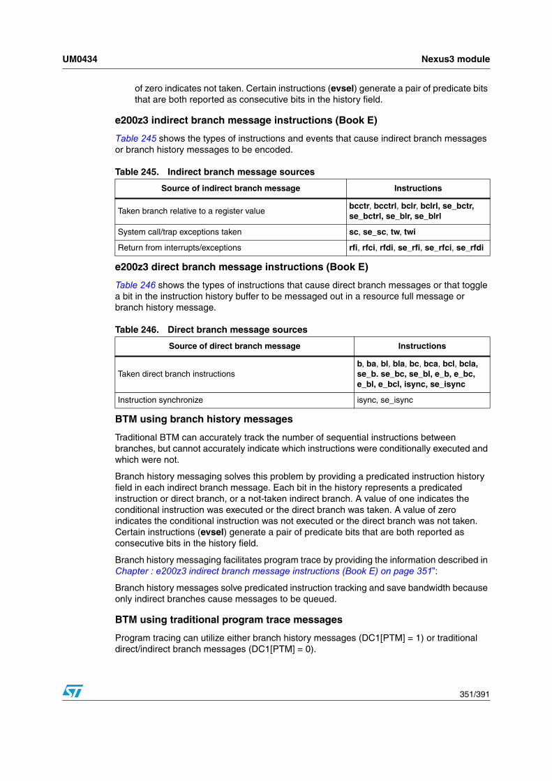
UM0434 Nexus3 module
351/391
of zero indicates not taken. Certain instructions (evsel) generate a pair of predicate bits that are both reported as consecutive bits in the history field.
e200z3 indirect branch message instructions (Book E)
Table 245 shows the types of instructions and events that cause indirect branch messages or branch history messages to be encoded.
e200z3 direct branch message instructions (Book E)
Table 246 shows the types of instructions that cause direct branch messages or that toggle a bit in the instruction history buffer to be messaged out in a resource full message or branch history message.
BTM using branch history messages
Traditional BTM can accurately track the number of sequential instructions between branches, but cannot accurately indicate which instructions were conditionally executed and which were not.
Branch history messaging solves this problem by providing a predicated instruction history field in each indirect branch message. Each bit in the history represents a predicated instruction or direct branch, or a not-taken indirect branch. A value of one indicates the conditional instruction was executed or the direct branch was taken. A value of zero indicates the conditional instruction was not executed or the direct branch was not taken. Certain instructions (evsel) generate a pair of predicate bits that are both reported as consecutive bits in the history field.
Branch history messaging facilitates program trace by providing the information described in Chapter : e200z3 indirect branch message instructions (Book E) on page 351”:
Branch history messages solve predicated instruction tracking and save bandwidth because only indirect branches cause messages to be queued.
BTM using traditional program trace messages
Program tracing can utilize either branch history messages (DC1[PTM] = 1) or traditional direct/indirect branch messages (DC1[PTM] = 0).
Table 245. Indirect branch message sources
Source of indirect branch message Instructions
Taken branch relative to a register valuebcctr, bcctrl, bclr, bclrl, se_bctr, se_bctrl, se_blr, se_blrl
System call/trap exceptions taken sc, se_sc, tw, twi
Return from interrupts/exceptions rfi, rfci, rfdi, se_rfi, se_rfci, se_rfdi
Table 246. Direct branch message sources
Source of direct branch message Instructions
Taken direct branch instructionsb, ba, bl, bla, bc, bca, bcl, bcla, se_b. se_bc, se_bl, e_b, e_bc, e_bl, e_bcl, isync, se_isync
Instruction synchronize isync, se_isync

Nexus3 module UM0434
352/391
Branch history saves bandwidth and keeps consistency between methods of program trace, yet may lose temporal order between BTM messages and other types of messages. Since direct branches are not messaged, but are instead included in the history field of the indirect branch history message, other types of messages may enter the FIFO between branch history messages. The development tool cannot determine the ordering of events that occurred with respect to direct branches simply by the order in which messages are sent out.
Traditional BTM messages maintain their temporal ordering because each event that can cause a message to be queued enters the FIFO in the order it occurred and is messaged out maintaining that order.
12.7.2 BTM message formats
The e200z3 Nexus3 block supports three types of traditional BTM messages: direct, indirect, and synchronized messages. It supports two types of branch history BTM messages: indirect branch history, and indirect branch history with synchronized messages. Debug status messages and error messages are also supported.
Indirect branch messages (History)
Indirect branches include all taken branches whose destination is determined at run time, interrupts, and exceptions. If DC1[PTM] is set, indirect branch information is messaged out in the format shown in Table 247:
Indirect branch messages (Traditional)
If DC1[PTM] is cleared, indirect branch information is messaged out in the format shown in Table 248:
Direct branch messages (Traditional)
Direct branches, conditional or unconditional, are all taken branches whose destinations are fixed in the instruction opcode. Direct branch information is messaged out in the format shown in Table 249:
Table 247. Indirect Branch Message (History) Format
(1–32 bits) (1–32 bits) (1–8 bits) (4 bits) (6 bits)
Branch History Relative AddressSequence
Count
Source Proces
s
TCODE (011100
)
Maximum length = 82 bit; Minimum length = 13 bits
Table 248. Indirect Branch Message Format
(1–32 bits) (1–8 bits) (4 bits) (6 bits)
Relative Address Sequence CountSource Process
TCODE (000100)
Maximum length = 50 bits; minimum length = 12 bits

UM0434 Nexus3 module
353/391
Note: When DC1[PTM] is set, direct branch messages are not transmitted. Instead, each direct branch or predicated instruction toggles a bit in the history buffer.
Resource full messages
The resource full message is used in conjunction with the branch history messages. The resource full message is generated when the internal branch/predicate history buffer is full. If synchronization is needed at the time this message is generated, the synchronization is delayed until the next branch trace message that is not a resource full message.
For history buffer overflow, the resource full message transmits a resource code (RCODE) of 0b0001 and the current contents of the history buffer, including the stop bit, are transmitted in the resource data (RDATA) field. This history information can be concatenated by the development tool with the branch/predicate history information from subsequent messages to obtain the complete branch/predicate history between indirect changes of flow.
For instruction counter overflow, the resource full message transmits an RCODE of 0b0000 and a value of 0xFF is transmitted in the RDATA field, indicating that 255 sequential instructions have been executed since the last change of flow or, if program trace is in history mode, since the last instruction that recorded history information
Table 250 shows the RCODE encodings and RDATA information used for Resource Full messages.
Debug status messages
Debug status messages report low-power mode and debug status. Debug status messages are enabled when Nexus 3 is enabled. Entering/exiting debug mode as well as entering a low-power mode triggers a debug status message, indicating the value of the most significant byte in the development status register. Debug status information is sent out in the format shown in Table 251:
Table 249. Direct Branch Message Format
(1–8 bits) (4 bits) (6 bits)
Sequence Count Source Process TCODE (000011)
Maximum Length = 18 bits; minimum length = 11 bits
Figure 73. Resource full message format
(1–32 bits) (4 bits) (4 bits) (6 bits)
Branch HistoryRCODE (0001)
Source Process
TCODE (011011)
Maximum length = 46 bits; minimum length = 15 bits
Table 250. RCODE encoding
RCODE RDATA field Description
0000 0xFFProgram trace instruction counter reached 255 and was reset.
0001Branch history. This type of packet is terminated by a stop bit set after the last history bit.
Program trace, branch/predicate instruction history full.

Nexus3 module UM0434
354/391
Program correlation messages
Program correlation messages (PCMs) are used to correlate events to the program flow that may not be associated with the instruction stream. The following events will result in a PCM when program trace is enabled:
● When the CPU enters debug mode, a PCM is generated. The instruction count and history information provided by the PCM can be used to determine the last sequence of instructions executed prior to debug mode entry.
● When the CPU enters a low power mode in which instructions are no longer executed, a PCM is generated. The instruction count and history information provided by the PCM can be used to determine the last sequence of instructions executed prior to low-power mode entry.
● Whenever program trace is disabled by any means, a PCM is generated. The instruction count and history information provided by the PCM can be used to determine the last sequence of instructions executed prior to disabling program trace. A second PCM is generated on this event if there has been an execution mode switch into or out of a sequence of VLE instructions. This VLE state information allows the development tool to interpret any preceding instruction count or history information in the proper context.
● Whenever the CPU crosses a page boundary that results in an execution mode switch into or out of a sequence of VLE instructions, a PCM is generated. The PCM effectively breaks up any running instruction count and history information between the two modes of operation so that the instruction count and history information can be processed by the development tool in the proper context.
● When using program trace in history mode, when a direct branch results in an execution mode switch into or out of a sequence of VLE instructions, a PCM is generated. The PCM effectively breaks up any running history information between the two modes of operation so that the history information can be processed by the development tool in the proper context.
Program correlation is messaged out in the format shown in Table 252:
BTM overflow error messages
An error message occurs when the message queue is full and a new message cannot be queued. The FIFO discards incoming messages until it has completely emptied the queue. Once emptied, an error message is queued. The error encoding indicates which types of messages attempted to be queued while the FIFO was being emptied.
Table 251. Debug status message format
(8 bits) (4 bits) (6 bits)
31–24 Source Process TCODE (000000)
Fixed length = 18 bits
Table 252. Program correlation message format
(1–32 bits) (1–8 bits) (4 bits) (4 bits) (6 bits)
Branch HistorySequence
CountECOD
ESource Process
TCODE (100001)
Maximum length = 54 bits; minimum length = 16 bits
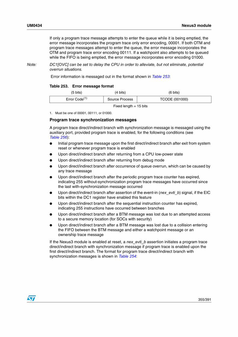
UM0434 Nexus3 module
355/391
If only a program trace message attempts to enter the queue while it is being emptied, the error message incorporates the program trace only error encoding, 00001. If both OTM and program trace messages attempt to enter the queue, the error message incorporates the OTM and program trace error encoding 00111. If a watchpoint also attempts to be queued while the FIFO is being emptied, the error message incorporates error encoding 01000.
Note: DC1[OVC] can be set to delay the CPU in order to alleviate, but not eliminate, potential overrun situations.
Error information is messaged out in the format shown in Table 253:
Program trace synchronization messages
A program trace direct/indirect branch with synchronization message is messaged using the auxiliary port, provided program trace is enabled, for the following conditions (see Table 256):
● Initial program trace message upon the first direct/indirect branch after exit from system reset or whenever program trace is enabled
● Upon direct/indirect branch after returning from a CPU low-power state
● Upon direct/indirect branch after returning from debug mode
● Upon direct/indirect branch after occurrence of queue overrun, which can be caused by any trace message
● Upon direct/indirect branch after the periodic program trace counter has expired, indicating 255 without-synchronization program trace messages have occurred since the last with-synchronization message occurred
● Upon direct/indirect branch after assertion of the event-in (nex_evti_b) signal, if the EIC bits within the DC1 register have enabled this feature
● Upon direct/indirect branch after the sequential instruction counter has expired, indicating 255 instructions have occurred between branches
● Upon direct/indirect branch after a BTM message was lost due to an attempted access to a secure memory location (for SOCs with security)
● Upon direct/indirect branch after a BTM message was lost due to a collision entering the FIFO between the BTM message and either a watchpoint message or an ownership trace message
If the Nexus3 module is enabled at reset, a nex_evti_b assertion initiates a program trace direct/indirect branch with synchronization message if program trace is enabled upon the first direct/indirect branch. The format for program trace direct/indirect branch with synchronization messages is shown in Table 254:
Table 253. Error message format
(5 bits) (4 bits) (6 bits)
Error Code(1)
1. Must be one of 00001, 00111, or 01000.
Source Process TCODE (001000)
Fixed length = 15 bits

Nexus3 module UM0434
356/391
The formats for program trace direct/indirect branch with synchronized messages and indirect branch history with synchronized messages are shown in Table 255:
Exceptions resulting in program trace synchronization are summarized in Table 256.
Table 254. Direct/Indirect branch with synchronization message format
(1–32 bits) (1–8 bits) (4 bits) (6 bits)
Full Target Address Sequence CountSource Process
TOCODE
(001011 or 001100)
Maximum length = 50 bits; minimum length = 12 bits
Table 255. Indirect branch history with synchronization message format
(1–32 bits) (1–32 bits) (1–8 bits) (4 bits) (6 bits)
Branch History Full Target AddressSequence
CountSource Process
TCODE (011101)
Maximum length = 82 bit; Minimum length = 13 bits
Table 256. Program trace exception summary
Exception condition
Exception handling
System reset negation
At the negation of JTAG reset, j_trst_b, queue pointers, counters, state machines, and registers within the Nexus3 module are reset. Upon the first branch out of system reset, if program trace is enabled, the first program trace message is a direct/indirect branch with synchronization message.
Program trace enabled
The first program trace message, after program trace has been enabled, is a synchronization message.
Exit from low power/debug
Upon exit from a low-power mode or debug mode, the next direct/indirect branch is converted to a direct/indirect branch with synchronization message.
Queue overrun
An error message occurs when the message queue is full and a new message cannot be queued. The FIFO discards messages until it has completely emptied the queue. Once emptied, an error message is queued. The error encoding indicates which types of messages attempted to be queued while the FIFO was being emptied. The next BTM message in the queue is a direct/indirect branch with synchronization message.
Periodic program trace synchronization
A forced synchronization occurs periodically after 255 program trace messages have been queued. A direct/indirect branch with synchronization message is queued. The periodic program trace message counter then resets.
Event in
If the Nexus module is enabled, assorting nex_evti_b initiates a direct/indirect branch with synchronization message upon the next direct/indirect branch, if program trace is enabled and the EIC bits of the DC1 register have enabled this feature.
Sequential instruction count overflow
When the sequential instruction counter reaches its maximum count (up to 255 sequential instructions may be executed), a forced synchronization occurs. The sequential counter then resets. A program trace direct/indirect branch with synchronization message is queued upon execution of the next branch.

UM0434 Nexus3 module
357/391
12.7.3 BTM operation
Enabling program trace
Both types of branch trace messaging can be enabled in one of two ways:
● Setting DC1[TM] to enable program trace
● Using WT[PTS] to enable program trace on watchpoint hits. e200z3 watchpoints are configured within the CPU.
Relative addressing
The relative address feature is compliant with the IEEE-ISTO 5001-2003 standard recommendations and is designed to reduce the number of bits transmitted for addresses of indirect branch messages.
The address transmitted is relative to the target address of the instruction that triggered the previous indirect branch or synchronized message. It is generated by XORing the new address with the previous address and then using only the results up to the most significant 1 bit in the result. To recreate this address, an XOR of the most significant zero-padded message address with the previously decoded address gives the current address. For the example given in Table 257, assume the previous address (A1) = 0x0003FC01, and the new address (A2) = 0x0003F365.
Attempted access to secure memory
For SOCs that implement security, any attempted branch to secure memory locations temporarily disables program trace and causes the corresponding BTM to be lost. The following direct/indirect branch queues a direct/indirect branch with synchronization message. The count value within this message will be inaccurate since the re-enable of program trace is not necessarily aligned on an instruction boundary.
Collision priority
All messages have the following priority: WPM → OTM → BTM → DTM. A BTM message that attempts to enter the queue at the same time as a watchpoint message or ownership trace message is lost. An error message is sent indicating the BTM was lost. The following direct/indirect branch queues a direct/indirect branch with synchronization message. The count value within this message reflects the number of sequential instructions executed after the last successful BTM message was generated. This count includes the branch that did not generate a message due to the collision.
Execution mode switch
Whenever the CPU switches execution mode into or out of a sequence of VLE instructions, the next branch trace message will be a Direct/Indirect Branch w/ Sync Message.
Table 256. Program trace exception summary (continued)
Exception condition
Exception handling

Nexus3 module UM0434
358/391
Execution mode indication
In order for a development tool to properly interpret instruction count and history information, it must be aware of the execution mode context of that information. VLE instructions will be interpreted differently from non-VLE instructions.
Program trace messages provide the execution mode status in the least significant bit of the reconstructed address field. A value of zero indicates that preceding instruction count and history information should be interpreted in a non-VLE context. A value of one indicates that the preceding instruction count and history information should be interpreted in a VLE context. Note that when a branch results in an execution mode switch, the program trace message resulting from that branch will indicate the previous execution state. The new state will not be signaled until the next program trace message.
In some cases, a program correlation message is generated to indicate execution mode status. Refer to Chapter : Program correlation messages on page 354,” for more information on these cases.
Branch/Predicate instruction history (HIST)
If DC1[PTM] is set, BTM messaging uses the branch history format. The branch history (HIST) packet in these messages provides a history of direct branch execution used for reconstructing program flow. This packet is implemented as a left-shifting shift register. The register is always pre-loaded with a value of one. This bit acts as a stop bit so that the development tools can determine which bit is the end of the history information. The pre-loaded bit itself is not part of the history but is transmitted with the packet.
A value of one is shifted into the history buffer on a taken branch, conditional or unconditional, and on any instruction whose predicate condition executed as true. A value of zero is shifted into the history buffer on any instruction whose predicate condition executed as false, as well as on branches not taken. This includes indirect as well as direct branches not taken. For the evsel instruction, two bits are shifted in, corresponding to the low element shifted in first, and the high element shifted in second.
Sequential instruction count (I-CNT)
The I-CNT packet is present in all BTM messages. For traditional branch messages, I-CNT represents the number of sequential instructions, or non-taken branches, in between direct/indirect branch messages.
Table 257. Relative address generation and re-creation example
Message generation
A1 0000 0000 0000 0011 1111 1100 0000 0001
A2 0000 0000 0000 0011 1111 0011 0110 0101
A1 ⊕ A2 0000 0000 0000 0000 0000 1111 0110 0100
M1(Address Message)
1111 0110 0100
Address Re-creation
A1 0000 0000 0000 0011 1111 1100 0000 0001
M1 0000 0000 0000 0000 0000 1111 0110 0100
A1 ⊕ M1 (A2) 0000 0000 0000 0011 1111 0011 0110 0101

UM0434 Nexus3 module
359/391
For branch history messages, I-CNT represents the number of instructions executed since the last taken/non-taken direct branch, predicate instruction, last taken/not-taken indirect branch, or exception. Branch instructions that trigger message generation are included in the I-CNT. Instructions that generate history bits are not included in the I-CNT.
The sequential instruction counter overflows when its value reaches 255 and is reset to 0. The next BTM message (corresponding to the 256th or later instruction) is converted to a synchronization type message.
Program trace queueing
Nexus3 implements a programmable depth queue (a minimum of 32 entries is recommended) for queuing all messages. Messages that enter the queue are transmitted through the auxiliary pins in the order in which they are queued.
Note: If multiple trace messages need to be queued at the same time, watchpoint messages have the highest priority:(WPM → OTM → BTM → DTM).
12.7.4 Program trace timing diagrams (2 MDO/1 MSEO Configuration)
Figure 74. Program trace—indirect branch message (traditional)
Figure 75. Program trace—indirect branch message (history)
00 01 00 00 00 00 00 00 10 01 01 10 10
TCODE = 4Source processor = 0000Number of sequential instructions = 128Relative address = 0xA5
00
MCKO
MSEO_B
MDO[1:0]
00 11 01 00 00 00 01 01 10 10 01 01 10
TCODE = 28Source processor = 0000Number of sequential instructions = 0Relative address = 0xA5Branch history = 010100101 (w/ stop)
10 00
MCKO
MSEO_B
MDO[1:0]
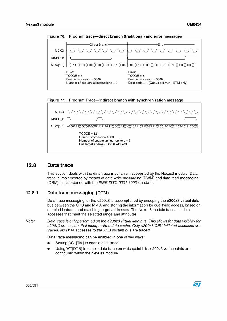
Nexus3 module UM0434
360/391
Figure 76. Program trace—direct branch (traditional) and error messages
Figure 77. Program Trace—Indirect branch with synchronization message
12.8 Data traceThis section deals with the data trace mechanism supported by the Nexus3 module. Data trace is implemented by means of data write messaging (DWM) and data read messaging (DRM) in accordance with the IEEE-ISTO 5001-2003 standard.
12.8.1 Data trace messaging (DTM)
Data trace messaging for the e200z3 is accomplished by snooping the e200z3 virtual data bus between the CPU and MMU, and storing the information for qualifying access, based on enabled features and matching target addresses. The Nexus3 module traces all data accesses that meet the selected range and attributes.
Note: Data trace is only performed on the e200z3 virtual data bus. This allows for data visibility for e200z3 processors that incorporate a data cache. Only e200z3 CPU-initiated accesses are traced. No DMA accesses to the AHB system bus are traced.
Data trace messaging can be enabled in one of two ways:
● Setting DC1[TM] to enable data trace.
● Using WT[DTS] to enable data trace on watchpoint hits. e200z3 watchpoints are configured within the Nexus1 module.
Direct Branch Error
11 00 00 00 00 11 00 00 10 00 00 00 01
DBM:TCODE = 3Source processor = 0000Number of sequential instructions = 3
Error:TCODE = 8Source processor = 0000Error code = 1 (Queue overrun—BTM only)
00 00
MCKO
MSEO_B
MDO[1:0]
00 11 00 00 00 11 10 11 00 11 10 10 11
TCODE = 12Source processor = 0000Number of sequential instructions = 3Full target address = 0xDEADFACE
11 01 11 10 10 10 11 01 11 00
MCKO
MSEO_B
MDO[1:0]

UM0434 Nexus3 module
361/391
12.8.2 DTM message formats
The Nexus3 block supports five types of DTM messages: data write, data read, data write synchronization, data read synchronization, and error messages.
Data write messages
The data write message contains the data write value and the address of the write access, relative to the previous data trace message. Data write message information is messaged out in the format shown in Table 258:
Data read messages
The data read message contains the data read value and the address of the read access, relative to the previous data trace message. Data read message information is messaged out in the format shown in Table 259:
Note: For e200z3-based CPUs, the double-word encoding, p_tsiz = 0, indicates a double-word access and is sent out as a single data trace message with a single 64-bit data value. The debug/development tool needs to distinguish between the two cases based on the family of e200z3 processors.
DTM overflow error messages
An error message occurs when the message queue is full and a new message cannot be queued. The FIFO discards incoming messages until it has completely emptied the queue. Once emptied, an error message is queued. The error encoding indicates which types of messages attempted to be queued while the FIFO was being emptied.
If only a DTM attempts to enter the queue while it is being emptied, the error message incorporates the data trace only error encoding 00010. If both OTM and DTM attempt to enter the queue, the error message incorporates the OTM and data trace error encoding, 00111. If a watchpoint also attempts to be queued while the FIFO is being emptied, the error message incorporates error encoding, 01000.
Note: DC1[OVC] can be set to delay the CPU in order to alleviate, but not eliminate, potential overrun situations.
Error information is messaged out in the format shown in Table 260:
Table 258. Data write message format
(1–64 bits) (1–32 bits)(3
bits)(4 bits) (6 bits)
Data Value(s) Relative AddressData Size
Source Process
TCODE (000101)
Maximum length = 109 bits; minimum length = 15 bits
Table 259. Data read message format
(1–64 bits) (1–32 bits)(3
bits)(4 bits) (6 bits)
Data Value(s) Relative AddressData Size
Source Process
TCODE (000110)
Maximum length = 109 bits; minimum length = 15 bits

Nexus3 module UM0434
362/391
Data trace synchronization messages
A data trace write/read with synchronization message is messaged through the auxiliary port, provided data trace is enabled, for the following conditions (see Table 262):
● Initial data trace message after exit from system reset or whenever data trace is enabled
● Upon returning from a CPU low-power state
● Upon returning from debug mode
● After occurrence of queue overrun (can be caused by any trace message), provided data trace is enabled
● After the periodic data trace counter has expired, indicating 255 data trace messages have occurred without synchronization since the last with-synchronization message occurred
● Upon assertion of the event-in nex_evti_b pin, the first data trace message is a synchronization message if the EIC bits of the DC1 register have enabled this feature.
● Upon data trace write/read after the previous DTM message was lost due to an attempted access to a secure memory location (for SOC’s with security)
● Upon data trace write/read after the previous DTM message was lost due to a collision entering the FIFO between the DTM message and any of the following:
– watchpoint message
– ownership trace message
– branch trace message
Data trace synchronization messages provide the full address, without leading zeros, and ensure that development tools fully synchronize with data trace regularly. Synchronization messages provide a reference address for subsequent DTMs, in which only the unique portion of the data trace address is transmitted. The format for data trace write/read with synchronization messages is as follows:
Exception conditions that result in data trace synchronization are summarized in Table 262.
Table 260. Error message format
(5 bits) (4 bits) (6 bits)
Error Code (00010/00111/01000 Source Process TCODE (001000)
Fixed length = 15 bits
Table 261. Data write/read with synchronization message format
(1–64 bits) (1–32 bits)(3
bits)(4 bits) (6 bits)
Data Value Full AddressData Size
Source Process
TCODE (001101 or 001110)
Maximum length = 109 bit; Minimum length = 15 bits

UM0434 Nexus3 module
363/391
12.8.3 DTM operation
DTM queueing
Nexus3 implements a programmable depth queue (a minimum of 32 entries is recommended) for queuing all messages. Messages that enter the queue are transmitted through the auxiliary pins in the order in which they are queued.
Note: If multiple trace messages need to be queued simultaneously, watchpoint messages have the highest priority:WPM → OTM → BTM → DTM. Up to two messages may be simultaneously queued.
Table 262. Data trace exception summary
Exception condition Exception handling
System reset negation
At the negation of JTAG reset (j_trst_b), queue pointers, counters, state machines, and registers within the Nexus3 module are reset. If data trace is enabled, the first data trace message is a data write/read with synchronization message.
Data trace enabledThe first data trace message (after data trace has been enabled) is a synchronization message.
Exit from low power/debug
Upon exit from a low-power mode or debug mode, the next data trace message is converted to a data write/read with synchronization message.
Queue overrun
An error message occurs when a new message cannot be queued due to the message queue being full. The FIFO discards messages until it has completely emptied the queue. Once emptied, an error message is queued. The error encoding indicates which type(s) of messages attempted to be queued while the FIFO was being emptied. The next DTM message in the queue will be a data write/read with synchronization message.
Periodic data trace synchronization
A forced synchronization occurs periodically after 255 data trace messages have been queued. A data write/read with synchronization message is queued. The periodic data trace message counter then resets.
Event in
If the Nexus module is enabled, a nex_evti_b assertion initiates a data trace write/read with synchronization message upon the next data write/read (if data trace is enabled and the EIC bits of the DC1 register have enabled this feature).
Attempted access to secure memory
For SOCs that implement security, any attempted read or write to secure memory locations temporarily disables data trace and causes the corresponding DTM to be lost. A subsequent read/write queues a data trace read/write with a synchronization message.
Collision priority
All messages have the following priority: WPM → OTM → BTM → DTM. A DTM message that attempts to enter the queue at the same time as a watchpoint message or ownership trace message or branch trace message will be lost. A subsequent read/write queues a data trace read/write with a synchronization message.

Nexus3 module UM0434
364/391
Relative addressing
The relative address feature is compliant with the IEEE-ISTO 5001-2003 standard recommendations and is designed to reduce the number of bits transmitted for addresses of data trace messages. Refer to Chapter : Relative addressing on page 357,” for details.
Data trace windowing
Data write/read messages are enabled by the RWT1n field in the data trace control register, DTC, for each DTM channel. Data trace windowing is achieved through the address range defined by the DTEA and DTSA registers and by DTC[RC1n]. All e200z3-initiated read/write accesses that fall inside or outside these address ranges, as programmed, are candidates to be traced.
Data Access/Instruction access data tracing
The Nexus3 module is capable of tracing both instruction access data or data access data. Each trace window can be configured for either type of data trace by setting the DI1n field within the data trace control register for each DTM channel.
e200z3 bus cycle special cases
Note: For a misaligned access that crosses a 64-bit boundary, the access is broken into two accesses. If both accesses are within the data trace range, two DTMs are sent: one with a size encoding indicating the size of the original access, that is, word, and one with a size encoding for the portion that crossed the boundary, that is, 3 bytes See Table 109: Invalid instruction forms on page 123 for examples of misaligned accesses.
Note: An STM (store) to the cache’s store buffer within the data trace range initiates a DTM message. If the corresponding memory access causes an error, a checkstop condition occurs. The debug/development tool should use this indication to invalidate the previous DTM.
Table 263. e200z3 bus cycle cases
Special case Action
e200z3 bus cycle aborted Cycle ignored
e200z3 bus cycle with data error (TEA) Data trace message discarded
e200z3 bus cycle completed without error Cycle captured and transmitted
e200z3 (AHB) bus cycle initiated by Nexus3 Cycle ignored
e200z3 bus cycle is an instruction fetch Cycle ignored
e200z3 bus cycle accesses misaligned data (across 64-bit boundary)—both first and second transactions within data trace range
First and second cycle captured and two DTMs transmitted
e200z3 bus cycle accesses misaligned data (across 64-bit boundary)—first transaction within data trace range; second transaction out of data trace range
First cycle captured and transmitted; second cycle ignored
e200z3 bus cycle accesses misaligned data (across 64-bit boundary)—first transaction out of data trace range; second transaction within data trace range
First cycle ignored; second cycle captured and transmitted

UM0434 Nexus3 module
365/391
12.8.4 Data trace timing diagrams (8 MDO/2 MSEO Configuration)
Figure 78. Data trace—data write message
Figure 79. Data trace—data read with synchronization message
Figure 80. Error message (data trace only encoded)
12.9 Watchpoint supportThis section details the watchpoint features of the Nexus3 module.
12.9.1 Overview
The Nexus3 module provides watchpoint messaging by means of the auxiliary pins, as defined by the IEEE-ISTO 5001-2003 standard.
Nexus3 is not compliant with class 4 breakpoint/watchpoint requirements defined in the standard. The breakpoint/watchpoint control register is not implemented.
1010100000000101 00010100 11101111
11 00 00 01 00
TCODE = 5Source processor = 0000Data size = 010 (half word)Relative address = 0xA5Write data = 0xBEEF
11
10111110
MCKO
MSEO_B[1:0]
MDO[7:0]
1100000000001110 01011001 11010001
11 00
TCODE = 14Source processor = 0000Data size = 000 (byte)Full access address = 0x01468ACEWrite data = 0x5C
00101000
01
00000000
11
01011100
MCKO
MSEO_B[1:0]
MDO[7:0]
0000100000001000
11 00 11
TCODE = 8Source processor = 0000Error code = 2 (queue overrun - DTM only)
xxxxxxxx
xx
MCKO
MSEO_B[1:0]
MDO[7:0]

Nexus3 module UM0434
366/391
12.9.2 Watchpoint messaging
Enabling watchpoint messaging is done by setting the watchpoint enable bit in the DC1 register. Setting the individual watchpoint sources is supported through the e200z3 Nexus1 module. The e200z3 Nexus1 module is capable of setting multiple address and/or data watchpoints. Please refer to Chapter 11: Debug support on page 296,” for details on watchpoint initialization.
When these watchpoints occur, a watchpoint event signal from the Nexus1 module causes a message to be sent to the queue to be messaged out. This message includes the watchpoint number indicating which watchpoint caused the message.
The occurrence of any of the e200z3-defined watchpoints can be programmed to assert the event out, nex_evto_b, pin for one period of the output clock, nex_mcko; see Table 271 for details on nex_evto_b.
Watchpoint information is messaged out in the format shown in Table 264:
Table 264. Watchpoint message format.
12.9.3 Watchpoint error message
An error message occurs when the message queue is full and a new message cannot be queued. The FIFO discards messages until it has completely emptied the queue. Once emptied, an error message is queued. The error encoding indicates which types of messages attempted to be queued while the FIFO was being emptied.
If only a watchpoint message attempts to enter the queue while it is being emptied, the error message incorporates the watchpoint-only error encoding, 00110. If an OTM and/or program trace and/or data trace message also attempts to enter the queue while it is being emptied, the error message incorporates error encoding 01000.
Note: DC1[OVC] can be set to delay the CPU in order to alleviate, but not eliminate, potential overrun situations.
(8 bit) (4 bits) (6 bits)
Watchpoint Source Source Process TCODE (001111)
Fixed length = 18 bits
Table 265. Watchpoint source encoding
Watchpoint source (8-Bits) Watchpoint description
0000_0001 e200z3 watchpoint #0 (IAC1 from Nexus1)
0000_0010 e200z3 watchpoint #1 (IAC2 from Nexus1)
0000_0100 e200z3 watchpoint #2 (IAC3 from Nexus1)
0000_1000 e200z3 watchpoint #3 (IAC4 from Nexus1)
0001_0000 e200z3 watchpoint #4 (DAC1 from Nexus1)
0010_0000 e200z3 watchpoint #5 (DAC2 from Nexus1)
0100_0000 e200z3 watchpoint #6 (DCNT1 from Nexus1)
1000_0000 e200z3 watchpoint #7 (DCNT2 from Nexus1)

UM0434 Nexus3 module
367/391
Error information is messaged out in the format, shown in Table 266:
12.9.4 Watchpoint timing diagram (2 MDO/1 MSEO Configuration)
Figure 81. Watchpoint message and watchpoint error message
12.10 Nexus3 Read/Write access to Memory-Mapped resourcesThe read/write access feature allows access to memory-mapped resources through the JTAG/OnCE port. The read/write mechanism supports single as well as block reads and writes to e200z3 AHB resources.
The Nexus3 module is capable of accessing resources on the e200z3 system bus, AHB, with multiple configurable priority levels. Memory-mapped registers and other non-cached memory can be accessed through the standard memory map settings.
All accesses are set up and initiated by the read/write access control/status register, RWCS, as well as RWA and RWD.
Using RWCS, RWA and RWD, memory-mapped e200z3 AHB resources can be accessed through Nexus3. The following sections describe the steps that are required to access memory-mapped resources.
Note: Read/write access can only access memory-mapped resources when system reset is de-asserted and clocks are running. Misaligned accesses are not supported in the e200z3 Nexus3 module.
12.10.1 Single write access
Note: In the first three steps, the registers are initialized using the access method outlined in Chapter 12.5: Nexus3 register access through JTAG/OnCE on page 348.”
Table 266. Error message format
(5 bits) (4 bits) (6 bits)
Error Code (00110/01000 Source Process TCODE (001000)
Fixed length = 15 bits
Watchpoint Error
11 11 00 00 10 00 00 00 10 00 00 10 01
WPM:TCODE = 15Source processor = 00Watchpoint number = 2
Error:TCODE = 8Source processor = 00Error code = 6 (Queue overrun—WPM only)
00
p_mcko
p_mseo_b
p_mdo[1:0]

Nexus3 module UM0434
368/391
1. Initialize RWA using the Nexus register index of 0x9; see Table 216. Configure as shown below:
– Write address = 0xnnnn_nnnn (write address)
2. Initialize RWCS using the Nexus register index of 0x7; see Table 216. Configure the fields as shown in Table 267:
Note: Access count (CNT) of 0x0000 or 0x0001 performs a single access.3. Initialize RWD using the Nexus register index of 0xA; see Table 216. Configure as
shown below:
– Write data = 0xnnnn_nnnn (write data)
4. The Nexus block then arbitrates for the AHB system bus and transfers the data value from the data buffer RWD register to the memory-mapped address in RWA. When the access has completed without error (ERR=0), Nexus asserts the nex_rdy_b signal (see Table 271 for detail on nex_rdy_b) and clears RWCS[DV]. This indicates that the device is ready for the next access.
Note: Only the nex_rdy_b signal and the DV and ERR fields within RWCS provide read/write access status to the external development tool.
12.10.2 Block write access (Non-Burst Mode)
1. For a non-burst block write access, follow Steps 1, 2, and 3 outlined in Chapter 12.10.1: Single write access on page 367,” to initialize the registers, but use a value greater than one (0x0001) for RWCS[CNT].
2. The Nexus block then arbitrates for the AHB system bus and transfers the first data value from the RWD register to the memory-mapped address in RWA. When the transfer has completed without error (ERR = 0), the address from the RWA register is incremented to the next word size (specified in RWCS[SZ]), and the number from the CNT field is decremented. Nexus then asserts the nex_rdy_b pin. This indicates that the device is ready for the next access.
3. Repeat step 3 in Chapter 12.10.1: Single write access on page 367,” until the internal CNT value is zero. When this occurs, RWCS[DV] is cleared to indicate the end of the block write access.
Table 267. Single write access field settings
Field Setting
AC (Access control) 1 (indicates start access)
MAP (Map select) 000 (primary memory map)
PR (Access priority) 00 (lowest priority)
RW (Read/write) 1 (write access)
SZ (Word size) 0nn (32-bit, 16-bit, 8-bit)
CNT (Access count) 0x0000 or 0x0001 (single access)

UM0434 Nexus3 module
369/391
12.10.3 Block write access (Burst Mode)
1. For a burst block write access, follow steps 1 and 2 outlined in Chapter 12.10.1: Single write access on page 367,” to initialize the registers, using a value of four (double-word) for RWCS[CNT] and an RWCS[SZ] value of 0b011, indicating 64-bit access.
2. Initialize the burst data buffer (RWD register) through the access method outlined in Chapter 12.5: Nexus3 register access through JTAG/OnCE on page 348,” using the Nexus register index of 0xA; see Table 216.
3. Repeat step 2 until all double-word values are written to the buffer.
Note: The data values must be shifted in 32 bits at a time, least significant bit first (that is, double-word write = two word writes to RWD).4. The Nexus block then arbitrates for the AHB system bus and transfers the burst data
values from the data buffer to the AHB beginning from the memory mapped address in RWA. For each access within the burst, the address from the RWA register is incremented to the next double-word size (as specified in RWCS[SZ]), modulo the length of the burst, and the number from the CNT field is decremented.
5. When the entire burst transfer has completed without error (ERR=0), Nexus3 then asserts the nex_rdy_b pin, and RWCS[DV] is cleared to indicate the end of the block write access.
Note: The actual RWA and RWCS[CNT] values are not changed when executing a block write access, burst or non-burst. The original values can be read by the external development tool at any time.
12.10.4 Single read access
1. Initialize RWA with the access method outlined in Chapter 12.5: Nexus3 register access through JTAG/OnCE on page 348,” using the Nexus register index of 0x9; see Table 216. Configure as shown below:
– Read address = 0xnnnn_nnnn (read address)
2. Initialize RWCS with the access method outlined in Chapter 12.5: Nexus3 register access through JTAG/OnCE on page 348,” using the Nexus register index of 0x7; see Table 216. Configure the bits as shown in Table 268:
Note: Access count (CNT) of 0x0000 or 0x0001 performs a single access. 3. The Nexus block then arbitrates for the AHB system bus and the read data is
transferred from the AHB to the RWD register. When the transfer is completed without error (ERR=0), Nexus asserts the nex_rdy_b pin (see Table 271 for details on
Table 268. Single read access parameter settings
Parameter Settings
Access control (AC) 1 (to indicate start access)
Map select (MAP) 000 (primary memory map)
Access priority (PR) 00 (lowest priority)
Read/write (RW) 0 (read access)
Word size (SZ) 0nn (32-bit, 16-bit, 8-bit)
Access count (CNT) 0x0000 or 0x0001(single access)

Nexus3 module UM0434
370/391
nex_rdy_b) and sets RWCS[DV]. This indicates that the device is ready for the next access.
4. The data can then be read from RWD with the access method outlined in Chapter 12.5: Nexus3 register access through JTAG/OnCE on page 348,” using the Nexus register index of 0xA; see Table 216.
Note: Only the nex_rdy_b signal and the DV and ERR bits within RWCS provide read/write access status to the external development tool.
12.10.5 Block read access (Non-Burst Mode)
1. For a non-burst block read access, follow steps 1 and 2 outlined in Chapter 12.10.4: Single read access on page 369,” to initialize the registers, but using a value greater than one (0x0001) for RWCS[CNT].
2. The Nexus block then arbitrates for the AHB system bus, and the read data is transferred from the AHB to the RWD register. When the transfer has completed without error (ERR = 0), the address from RWA is incremented to the next word size (specified in the SZ field), and the number from the CNT field is decremented. Nexus then asserts the nex_rdy_b pin. This indicates that the device is ready for the next access.
3. The data can then be read from RWD with the access method outlined in Chapter 12.5: Nexus3 register access through JTAG/OnCE on page 348,” using the Nexus register index of 0xA, see Table 216.
4. Repeat steps 3 and 4 in Chapter 12.10.4: Single read access on page 369,” until the CNT value is zero. When this occurs, RWCS[DV] is set to indicate the end of the block read access.
12.10.6 Block read access (Burst Mode)
1. For a burst block read access, follow steps 1 and 2 outlined in Chapter 12.10.4: Single read access on page 369,” to initialize the registers, using a value of four (double-words) for the CNT field and an SZ field indicating 64-bit access in RWCS.
2. The Nexus block then arbitrates for the AHB system bus and the burst read data is transferred from the AHB to the data buffer (RWD register). For each access within the burst, the address from the RWA register is incremented to the next double-word, specified in the SZ field, and the number from the CNT field is decremented.
3. When the entire burst transfer has completed without error (ERR=0), Nexus then asserts the nex_rdy_b pin, and RWCS[DV] is set to indicate the end of the block read access.
4. The data can then be read from the burst data buffer (RWD register) with the access method outlined in Chapter 12.5: Nexus3 register access through JTAG/OnCE on page 348,” using the Nexus register index of 0xA; see Table 216.
5. Repeat step 3 until all double-word values are read from the buffer.
Note: The data values must be shifted out 32-bits at a time, least significant bit first, that is double-word read = two word reads from RWD.
Note: The actual RWA and CNT values within RWCS are not changed when executing a block read access, burst or non-burst. The original values can be read by the external development tool at any time.

UM0434 Nexus3 module
371/391
12.10.7 Error handling
The Nexus3 module handles various error conditions as described in the following sections.
AHB Read/Write error
All address and data errors that occur on read/write accesses to the e200z3 AHB system bus return a transfer error encoding on the p_hresp[1:0] signals. If this occurs, the following steps are taken:
1. The access is terminated without retrying, and RWCS[AC] is cleared.
2. RWCS[ERR] is set.
3. The error message is sent, TCODE = 8, indicating read/write error.
Access termination
The following cases are defined for sequences of the read/write protocol that differ from those described in the above sections.
1. If RWCS[AC] is set to start read/write accesses and invalid values are loaded into RWD or RWA, an AHB access error may occur. This is handled as described above.
2. If a block access is in progress, all cycles are not completed, and the RWCS register is written. The original block access is terminated at the boundary of the nearest completed access.
a) If RWCS[AC] is set, the next read/write access begins and the RWD can be written to / read from.
b) If RWCS[AC] is cleared, the read/write access is terminated at the nearest completed access. This method can be used to break block accesses or terminate them early.
Read/Write access error message
The read/write access error message is sent out when an AHB system bus access error, read or write, has occurred.
Error information is messaged out in the format shown in Table 269:
12.11 Nexus3 pin interfaceThis section details the Nexus3 pins and pin protocol.
The Nexus3 pin interface provides the function of transmitting messages from the message queue to the external tools. It is also responsible for handshaking with the message queue.
12.11.1 Pins implemented
The Nexus3 module implements one nex_evti_b and either one nex_mseo_b or two nex_mseo_b[1:0]. It also implements a configurable number of nex_mdo[n:0] pins,
Table 269. Error message format
(5 bits) (4 bits) (6 bits)
Error Code (00011) Source Process TCODE (001000)
Fixed length = 15 bits

Nexus3 module UM0434
372/391
nex_rdy_b pin, nex_evto_b pin, and one clock output pin, nex_mcko. The output pins are synchronized to the Nexus3 output clock, nex_mcko.
All Nexus3 input functionality is controlled through the JTAG/OnCE port, in compliance with IEEE 1149.1. (See Chapter 12.5: Nexus3 register access through JTAG/OnCE on page 348,” for details.) The JTAG pins are incorporated as I/O to the e200z3 processor and are further described in Chapter 11.5.2: JTAG/OnCE signals on page 308.”
The auxiliary pins are used to send and receive messages and are described in Table 271.
Table 270. JTAG pins for Nexus3
JTAG pin I/O Description of JTAG pins (included in e200z3 Nexus1)
j_tdo OTest data output. j_tdo is the serial output for test instructions and data. It is three-statable and is actively driven in the shift-IR and shift-DR controller states. It changes on the falling edge of j_tclk.
j_tdi ITest data input. j_tdi receives serial test instruction and data. TDI is sampled on the rising edge of j_tclk.
j_tms ITest mode select. Input pin used to sequence the OnCE controller state machine. j_tms is sampled on the rising edge of j_tclk.
j_tclk ITest clock. Input pin used to synchronize the test logic and control register access through the JTAG/OnCE port.
j_trst_b ITest reset. Input pin used to asynchronously initialize the JTAG/OnCE controller.
Table 271. Nexus3 auxiliary pins
Auxiliary pin I/O Description of auxiliary pins
nex_mcko OMessage clock out. A free running output clock to development tools for timing of nex_mdo[n:0] and nex_mseo_b[1:0] pin functions. nex_mcko is programmable through the DC1 register.
nex_mdo[n–0] OMessage data out. Used for OTM, BTM, and DTM. External latching of nex_mdo[n:0] occurs on the rising edge of the Nexus3 clock (nex_mcko).
nex_mseo_b[1–0] O
Message start/end out. Indicate when a message on the nex_mdo[n:0] pins has started, when a variable length packet has ended, and when the message has ended. External latching of nex_mseo_b[1–0] occurs on the rising edge of the Nexus3 clock (nex_mcko). One- or two-pin MSEO functionality is determined at integration time according to the SOC implementation
nex_rdy_b O
Ready. Used to indicate to the external tool that the Nexus block is ready for the next read/write access. If Nexus is enabled, this signal is asserted upon successful completion (without error) of an AHB system bus transfer (Nexus read or write) and is held asserted until the JTAG/OnCE state machine reaches the capture_dr state. Upon exit from system reset or if Nexus is disabled, nex_rdy_b remains de-asserted.

UM0434 Nexus3 module
373/391
The Nexus auxiliary port arbitration pins are used when the Nexus3 module is implemented in a multiple Nexus SoC that shares a single auxiliary output port. The arbitration is controlled by an SoC-level Nexus port control module (NPC). Refer to Chapter 12.13: Auxiliary port arbitration on page 376,” for details on Nexus port arbitration.
12.11.2 Pin protocol
The protocol for the e200z3 processor transmitting messages through the auxiliary pins is accomplished with the MSEO pin function outlined in Table 273. Both single- and dual-pin cases are shown.
nex_mseo_b[1:0] is used to signal the end of variable-length packets, and not fixed length packets. nex_mseo_b[1:0] is sampled on the rising edge of the Nexus3 clock, nex_mcko.
nex_evto_b O
Event out. An output whose assertion indicates that one of two events has occurred based on the bits in DC1[EOC]. nex_evto_b is held asserted for 1 cycle of nex_mcko:
– One (or more) watchpoints has occurred (from Nexus1) and EOC = 00
– Debug mode was entered (jd_debug_b asserted from Nexus1) and EOC = 01
nex_evti_b I
Event in. An input whose assertion initiates one of two events based on DC1[EIC] (if the Nexus module is enabled at reset):– Program trace and data trace synchronization messages (provided
program trace and data trace are enabled and EIC = 00).– Debug request to e200z3 Nexus1 module (provided EIC = 01 and
this feature is implemented).
Table 272. Nexus port arbitration signals
Nexus Port Arbitration pins
Input/Output
Description of arbitration pins
nex_aux_req[1:0] O
Nexus auxiliary request. Output signals indicating to an SoC level Nexus arbiter a request for access to the shared Nexus auxiliary port in a multiple Nexus implementation. The priority encodings are determined by how many messages are currently in the message queues, see Table 274).
nex_aux_busy ONexus auxiliary busy. An output signal to an SoC level Nexus arbiter indicating that the Nexus3 module is currently transmitting its message after being granted the Nexus auxiliary port.
npc_aux_grant INexus auxiliary grant. An input from the SoC level Nexus port controller (NPC) indicating that the auxiliary port has been granted to the Nexus3 module to transmit its message.
ext_multi_nex_sel I
Multiple Nexus select. A static signal indicating that the Nexus3 module is implemented within a multiple Nexus environment. If set, port control and arbitration is controlled by the SoC-level arbitration module (NPC).
Table 271. Nexus3 auxiliary pins (continued)
Auxiliary pin I/O Description of auxiliary pins

Nexus3 module UM0434
374/391
Figure 82. State diagram for single pin MSEO transfers
Note that the end message state does not contain valid data on nex_mdo[n:0]. Also, it is not possible to have two consecutive end packet messages. This implies the minimum packet size for a variable length packet is 2x the number of nex_mdo[n:0] pins. This ensures that a false end-of-message state is not entered by emitting two consecutive 1s on nex_mseo_b before the actual end of message.
Figure 83 shows the state diagram for dual-pin MSEO transfers.
Table 273. MSEO Pin(s) protocol
nex_mseo_b functionSingle nex_mseo_b data
(serial)Dual nex_mseo_b[1:0] data
Start of message 1–1–0 11–00
End of message 0–1–1–(more ones) 00 (or 01)–11–(more ones)
End of variable length packet 0–1–0 00–01
Message transmission 0s 00s
Idle (no message) 1s 11s
Normal
Transfer
nex_mseo_b=1
nex_mseo_b=1
nex_mseo_b=0
nex_mseo_b=0
nex_mseo_b=1
nex_mseo_b=1
nex_mseo_b=0
nex_mseo_b=0
nex_mseo_b=0nex_mseo_b=1
Not Allowed
End
Packet
Idle
MDO: Invalid
Stage
Message
End
MessageMDO: Invalid

UM0434 Nexus3 module
375/391
Figure 83. Dual-Pin MSEO transfers
The dual-pin MSEO option is more robust than the single-pin option. Termination of the current message may immediately be followed by the start of the next message on consecutive clocks. An extra clock to end the message is not necessary as with the one MSEO pin option. The dual-pin option also allows for consecutive end packet states. This can be an advantage when small, variable sized packets are transferred.
Note: The end message state may also indicate the end of a variable-length packet as well as the end of the message when using the dual-pin option.
12.12 Rules for output messagese200z3-based class 3–compliant embedded processors must provide messages through the auxiliary port in a consistent manner as described below:
● A variable-length packet within a message must end on a port boundary.
● A variable-length packet may start within a port boundary only when following a fixed-length packet. If two variable-length packets end and start on the same clock, it is impossible to know which bit is from the last packet and which bit is from the next packet.
● Whenever a variable-length packet is sized such that it does not end on a port boundary, it is necessary to extend and zero-fill the remaining bits after the highest order bit so that it can end on a port boundary.
Normal
Transfer
End
Message
nex_mseo_b[1:0]=11
nex_mseo_b[1:0]=11
nex_mseo_b[1:0]=00
nex_mseo_b[1:0]=00
nex_mseo_b[1:0]=01
nex_mseo_b[1:0]=01
nex_mseo_b[1:0]=00
nex_mseo_b[1:0]=00
nex_mseo_b[1:0]=00
nex_mseo_b[1:0]=11
nex_mseo_b[1:0]=01
End
Packet
nex_mseo_b[1:0]=11
nex_mseo_b[1:0]=11
nex_mseo_b[1:0]=10
Start
Message
nex_mseo_b[1:0]=10
nex_mseo_b[1:0]=10
nex_mseo_b[1:0]=01
nex_mseo_b[1:0]=01
Idle
MDO: Invalid

Nexus3 module UM0434
376/391
For example, if the nex_mdo[n:0] port is 2 bits wide and the unique portion of an indirect address TCODE is 5 bits, the remaining 1 bit of nex_mdo[n:0] must be packed with a zero.
12.13 Auxiliary port arbitrationIn a multiple Nexus environment, the Nexus3 module must arbitrate for the shared Nexus port at the SoC level.The request scheme is implemented as a 2-bit request with various levels of priority. The priority levels are defined in Table 274 below. The Nexus3 module receives a 1-bit grant signal (npc_aux_grant) from the SoC level arbiter. When a grant is received, the Nexus3 module begins transmitting its message following the protocol outlined in Chapter 12.11.2: Pin protocol on page 373.” The Nexus3 module maintains control of the port, by asserting the nex_aux_busy signal, until the MSEO state machine reaches the end message state.
12.14 ExamplesThe following are examples of program trace and data trace messages.
Table 275 shows an example of an indirect branch message with 2 MDO/1 MSEO configuration. Table 276 shows the same example with an 8 MDO/2 MSEO configuration.
Note: During clock 12, the nex_mdo[n:0] pins are ignored in the single MSEO case.
Table 274. MDO request encodings
Request levelMDO request
Encoding(nex_aux_req[1:0])Condition of queue
No request 00 No message to send
Low priority 01 Message queue less than half full
— 10 Reserved
High priority 11 Message queue at least half full

UM0434 Nexus3 module
377/391
T0 and S0 are the least significant bits, where Tx = TCODE number (fixed); Sx = source processor (fixed); Ix = number of instructions (variable); Ax = unique portion of the address (variable).
T0 and S0 are the least significant bits, where Tx = TCODE number (fixed); Sx = source processor (fixed); Ix = number of instructions (variable); Ax = unique portion of the address (variable).
Table 278 shows examples of direct branch messages: one with 2 MDO/1 MSEO, and one with 8 MDO/2 MSEO.
Table 275. Indirect branch message example (2 MDO/1 MSEO)
Clock nex_mdo[1:0] nex_mseo_b State
0 X X 1 Idle (or end of last message)
1 T1 T0 0 Start message
2 T3 T2 0 Normal transfer
3 T5 T4 0 Normal transfer
4 S1 S0 0 Normal transfer
5 S3 S2 0 Normal transfer
6 I1 I0 0 Normal transfer
7 I3 I2 0 Normal transfer
8 I5 I4 1 End packet
9 A1 A0 0 Normal transfer
10 A3 A2 0 Normal transfer
11 A5 A4 0 Normal transfer
12 A7 A6 1End packet
During clock 12, the nex_mdo[n:0] pins are ignored in the single-MSEO case.
13 0 0 1 End message
14 T1 T0 0 Start message
Table 276. Indirect branch message example (8 MDO/2 MSEO)
Clock nex_mdo[7:0] nex_mseo_b[1:0] State
0 X X X X X X X X 1 1Idle (or end of last message)
1 S1 S0 T5 T4 T3 T2 T1 T0 0 0 Start message
2 I5 I4 I3 I2 I1 I0 S3 S2 0 1 End packet
3 A7 A6 A5 A4 A3 A2 A1 A0 1 1 End packet/end message
4 S1 S0 T5 T4 T3 T2 T1 T0 0 0 Start message

Nexus3 module UM0434
378/391
T0, A0 and S0 are the least significant bits, where Tx = TCODE number (fixed); Sx = source processor (fixed); Zx = data size (fixed); Ax = unique portion of address (variable); Dx = Write data (variable-8,16 or 32-bit).
T0 and S0 are the least significant bits, where Tx = TCODE number (fixed); Sx = source processor (fixed); Ix = number of instructions (variable); Ax = unique portion of the address (variable).
Table 279 shows an example of a data write message with 8 MDO/1 MSEO configuration, and Table 280 shows the same DWM with 8 MDO/2 MSEO configuration.
T0, A0 and S0 are the least significant bits, where Tx = TCODE number (fixed); Sx = source processor (fixed); Zx = data size (fixed); Ax = unique portion of address (variable); Dx = Write data (variable-8,16 or 32-bit).
Table 277. Direct branch message example (2 MDO/1 MSEO)
Clock nex_mdo[1:0] nex_mseo_b State
0 X X 1 Idle (or end of last message)
1 T1 T0 0 Start message
2 T3 T2 0 Normal transfer
3 T5 T4 0 Normal transfer
4 S1 S0 0 Normal transfer
5 S3 S2 0 Normal transfer
6 I1 I0 1 End packet
7 0 0 1 End message
Table 278. Direct branch message example (8 MDO / 2 MSEO)
Clock nex_mdo[7:0] nex_mseo_b[1:0] State
0 X X X X X X X X 1 1 Idle (or end of last message)
1 S1 S0 T5 T4 T3 T2 T1 T0 0 0 Start message
2 0 0 0 0 I1 I0 S3 S2 1 1 End packet/end message
3 S1 S0 T5 T4 T3 T2 T1 T0 0 0 Start message
Table 279. Data write message example (8 MDO/1 MSEO)
Clock nex_mdo[7:0] nex_mseo_b State
0 X X X X X X X X 1 Idle (or end of last message)
1 S1 S0 T5 T4 T3 T2 T1 T0 0 Start message
2 A2 A1 A0 Z2 Z1 Z0 S3 S2 1 End packet
3 D7 D6 D5 D4 D3 D2 D1 D0 0 Normal transfer
4 0 0 0 0 0 0 0 0 1 End packet
5 0 0 0 0 0 0 0 0 1 End message
Table 280. Data write message example (8 MDO/2 MSEO)
Clock nex_mdo[7:0] nex_mseo_b[1:0] State
0 X X X X X X X X 1 1 Idle (or end of last message)
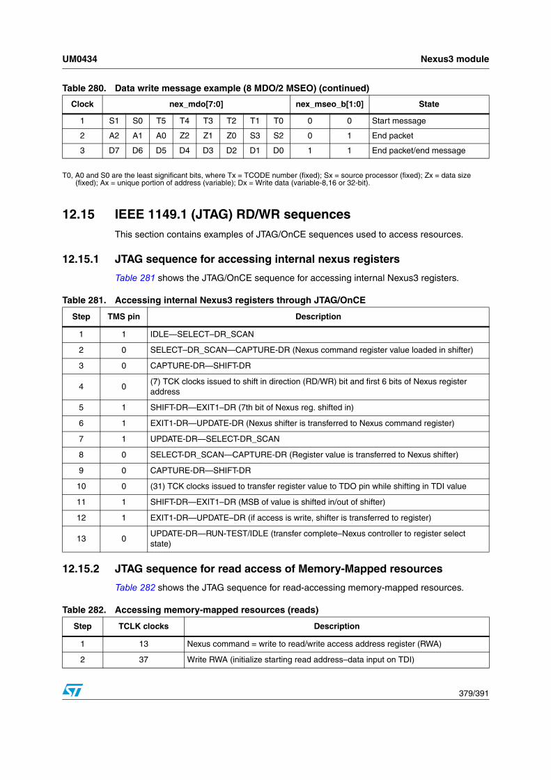
UM0434 Nexus3 module
379/391
T0, A0 and S0 are the least significant bits, where Tx = TCODE number (fixed); Sx = source processor (fixed); Zx = data size (fixed); Ax = unique portion of address (variable); Dx = Write data (variable-8,16 or 32-bit).
12.15 IEEE 1149.1 (JTAG) RD/WR sequencesThis section contains examples of JTAG/OnCE sequences used to access resources.
12.15.1 JTAG sequence for accessing internal nexus registers
Table 281 shows the JTAG/OnCE sequence for accessing internal Nexus3 registers.
12.15.2 JTAG sequence for read access of Memory-Mapped resources
Table 282 shows the JTAG sequence for read-accessing memory-mapped resources.
1 S1 S0 T5 T4 T3 T2 T1 T0 0 0 Start message
2 A2 A1 A0 Z2 Z1 Z0 S3 S2 0 1 End packet
3 D7 D6 D5 D4 D3 D2 D1 D0 1 1 End packet/end message
Table 280. Data write message example (8 MDO/2 MSEO) (continued)
Clock nex_mdo[7:0] nex_mseo_b[1:0] State
Table 281. Accessing internal Nexus3 registers through JTAG/OnCE
Step TMS pin Description
1 1 IDLE—SELECT–DR_SCAN
2 0 SELECT–DR_SCAN—CAPTURE-DR (Nexus command register value loaded in shifter)
3 0 CAPTURE-DR—SHIFT-DR
4 0(7) TCK clocks issued to shift in direction (RD/WR) bit and first 6 bits of Nexus register address
5 1 SHIFT-DR—EXIT1–DR (7th bit of Nexus reg. shifted in)
6 1 EXIT1-DR—UPDATE-DR (Nexus shifter is transferred to Nexus command register)
7 1 UPDATE-DR—SELECT-DR_SCAN
8 0 SELECT-DR_SCAN—CAPTURE-DR (Register value is transferred to Nexus shifter)
9 0 CAPTURE-DR—SHIFT-DR
10 0 (31) TCK clocks issued to transfer register value to TDO pin while shifting in TDI value
11 1 SHIFT-DR—EXIT1–DR (MSB of value is shifted in/out of shifter)
12 1 EXIT1-DR—UPDATE–DR (if access is write, shifter is transferred to register)
13 0UPDATE-DR—RUN-TEST/IDLE (transfer complete–Nexus controller to register select state)
Table 282. Accessing memory-mapped resources (reads)
Step TCLK clocks Description
1 13 Nexus command = write to read/write access address register (RWA)
2 37 Write RWA (initialize starting read address–data input on TDI)

Nexus3 module UM0434
380/391
12.15.3 JTAG sequence for write access of Memory-Mapped resources
Table 283 shows the JTAG sequence for write-accessing memory-mapped resources.
3 13 Nexus command = write to read/write control/status register (RWCS)
4 37 Write RWCS (initialize read access mode and CNT value–data input on TDI)
5 — Wait for falling edge of nex_rdy_b pin
6 13 Nexus command = read read/write access data register (RWD)
7 37 Read RWD (data output on TDO)
8 — If CNT > 0, go back to Step 5
Table 282. Accessing memory-mapped resources (reads) (continued)
Step TCLK clocks Description
Table 283. Accessing memory-mapped resources (writes)
Step TCLK clocks Description
1 13 Nexus command = write to read/write access control/status register (RWCS)
2 37 Write RWCS (initialize write access mode and CNT value–data input on TDI)
3 13 Nexus command = write to read/write address register (RWA)
4 37 Write RWA (initialize starting write address–data input on TDI)
5 13 Nexus command = read read/write access data register (RWD)
6 37 Write RWD (data output on TDO)
7 — Wait for falling edge of nex_rdy_b pin
8 — If CNT > 0, go back to Step #5

UM0434 Glossary
381/391
13 Glossary
The glossary contains an alphabetical list of terms, phrases, and abbreviations used in this book. Some of the terms and definitions included in the glossary are reprinted from IEEE Standard 754-1985, IEEE Standard for Binary Floating-Point Arithmetic, copyright ©1985 by the Institute of Electrical and Electronics Engineers, Inc. with the permission of the IEEE.
AArchitecture. A detailed specification of requirements for a processor or computer system. It does not specify details of how the processor or computer system must be implemented; instead it provides a template for a family of compatible implementations.
Asynchronous interrupt.
interrupts that are caused by events external to the processor’s execution. In this document, the term asynchronous interrupt is used interchangeably with the word interrupt.
Atomic access. A bus access that attempts to be part of a read-write operation to the same address uninterrupted by any other access to that address (the term refers to the fact that the transactions are indivisible). The PowerPC architecture implements atomic accesses through the lwarx/stwcx. instruction pair.
BBiased exponent. An exponent whose range of values is shifted by a constant (bias). Typically a bias is provided to allow a range of positive values to express a range that includes both positive and negative values.
Big-endian. A byte-ordering method in memory where the address n of a word corresponds to the most-significant byte. In an addressed memory word, the bytes are ordered (left to right) 0, 1, 2, 3, with 0 being the most-significant byte. See Little-endian.
Boundedly undefined. A characteristic of certain operation results that are not rigidly prescribed by the PowerPC architecture. Boundedly- undefined results for a given operation may vary among implementations and between execution attempts in the same implementation.
Although the architecture does not prescribe the exact behavior for when results are allowed to be boundedly undefined, the results of executing instructions in contexts where results are allowed to be boundedly undefined are constrained to ones that could have been achieved by executing an arbitrary sequence of defined instructions, in valid form, starting in the state the machine was in before attempting to execute the given instruction.
Branch prediction. The process of guessing whether a branch will be taken. Such predictions can be correct or incorrect; the term ‘predicted’ as it is used here does not imply that the prediction is correct (successful). The PowerPC architecture defines a means for static branch prediction as part of the instruction encoding.
Branch resolution. The determination of whether a branch is taken or not taken. A branch is said to be resolved when the processor can determine which instruction path to take. If the branch is resolved as predicted, the instructions following the predicted branch that may have been speculatively executed can complete (see Completion). If the branch is not resolved as predicted, instructions on the mispredicted path, and any results of speculative execution, are purged from the pipeline and fetching continues from the nonpredicted path.

Glossary UM0434
382/391
CCache. High-speed memory containing recently accessed data or instructions (subset of main memory).
Cache block. A small region of contiguous memory that is copied from memory into a cache. The size of a cache block may vary among processors; the maximum block size is one page. In PowerPC processors, cache coherency is maintained on a cache-block basis. Note that the term cache block is often used interchangeably with ‘cache line.’
Cache coherency. An attribute wherein an accurate and common view of memory is provided to all devices that share the same memory system. Caches are coherent if a processor performing a read from its cache is supplied with data corresponding to the most recent value written to memory or to another processor’s cache.
Cache flush. An operation that removes from a cache any data from a specified address range. This operation ensures that any modified data within the specified address range is written back to main memory. This operation is generated typically by a Data Cache Block Flush (dcbf) instruction.
Caching-inhibited. A memory update policy in which the cache is bypassed and the load or store is performed to or from main memory.
Cast out. A cache block that must be written to memory when a cache miss causes a cache block to be replaced.
Changed bit. One of two page history bits found in each page table entry (PTE). The processor sets the changed bit if any store is performed into the page. See also Page access history bits and Referenced bit.
Clean. An operation that causes a cache block to be written to memory, if modified, and then left in a valid, unmodified state in the cache.
Clear. To cause a bit or bit field to register a value of zero. See also Set.
Completion. Completion occurs when an instruction has finished executing, written back any results, and is removed from the completion queue (CQ). When an instruction completes, it is guaranteed that this instruction and all previous instructions can cause no interrupts.
Context synchronization. An operation that ensures that all instructions in execution complete past the point where they can produce an interrupt, that all instructions in execution complete in the context in which they began execution, and that all subsequent instructions are fetched and executed in the new context. Context synchronization may result from executing specific instructions (such as isync or rfi) or when certain events occur (such as an interrupt).
Copy-back operation. A cache operation in which a cache line is copied back to memory to enforce cache coherency. Copy-back operations consist of snoop push-out operations and cache cast-out operations.
DDenormalized number. A nonzero floating-point number whose exponent has a reserved value, usually the format's minimum, and whose explicit or implicit leading significand bit is zero.

UM0434 Glossary
383/391
EEffective address (EA). The 32-bit address specified for a load, store, or an instruction fetch. This address is then submitted to the MMU for translation to either a physical memory address or an I/O address.
Exception. A condition that, if enabled, generates an interrupt.
Execution synchronization. A mechanism by which all instructions in execution are architecturally complete before beginning execution (appearing to begin execution) of the next instruction. Similar to context synchronization but doesn't force the contents of the instruction buffers to be deleted and refetched.
Exponent. In the binary representation of a floating-point number, the exponent is the component that normally signifies the integer power to which the value two is raised in determining the value of the represented number. See also Biased exponent.
FFall-through (branch fall-through). A not-taken branch.
Fetch. Retrieving instructions from either the cache or main memory and placing them into the instruction queue.
Finish. Finishing occurs in the last cycle of execution. In this cycle, the CQ entry is updated to indicate that the instruction has finished executing.
Flush. An operation that causes a cache block to be invalidated and the data, if modified, to be written to memory.
Fraction. In the binary representation of a floating-point number, the field of the significand that lies to the right of its implied binary point.
GGeneral-purpose register (GPR). Any of the 32 registers in the general-purpose register file. These registers provide the source operands and destination results for all integer data manipulation instructions. Integer load instructions move data from memory to GPRs and store instructions move data from GPRs to memory.
Guarded. The guarded attribute pertains to out-of-order execution. When a page is designated as guarded, instructions and data cannot be accessed out-of-order.
HHarvard architecture. An architectural model featuring separate caches and other memory management resources for instructions and data.
Hashing. An algorithm used in the page table search process.
IIEEE 754. A standard written by the Institute of Electrical and Electronics Engineers that defines operations and representations of binary floating-point numbers.
Illegal instructions. A class of instructions that are not implemented for a particular PowerPC processor. These include instructions not defined by the PowerPC architecture. In

Glossary UM0434
384/391
addition, for 32-bit implementations, instructions that are defined only for 64-bit implementations are considered to be illegal instructions. For 64-bit implementations instructions that are defined only for 32-bit implementations are considered to be illegal instructions.
Implementation. A particular processor that conforms to the PowerPC architecture, but may differ from other architecture-compliant implementations for example in design, feature set, and implementation of optional features. The PowerPC architecture has many different implementations.
Imprecise interrupt. A type of synchronous interrupt that is allowed not to adhere to the precise interrupt model (see Precise interrupt). The PowerPC architecture allows only floating-point exceptions to be handled imprecisely.
Instruction queue. A holding place for instructions fetched from the current instruction stream.
Integer unit. The functional unit in the processor responsible for executing all integer instructions.
In-order. An aspect of an operation that adheres to a sequential model. An operation is said to be performed in-order if, at the time that it is performed, it is known to be required by the sequential execution model. See Out-of-order.
Instruction latency. The total number of clock cycles necessary to execute an instruction and make ready the results of that instruction.
Interrupt. A condition encountered by the processor that requires special, supervisor-level processing.
Interrupt handler. A software routine that executes when an interrupt is taken. Normally, the interrupt handler corrects the condition that caused the interrupt, or performs some other meaningful task (that may include aborting the program that caused the interrupt).
KKill. An operation that causes a cache block to be invalidated without writing any modified data to memory.
LLatency. The number of clock cycles necessary to execute an instruction and make ready the results of that execution for a subsequent instruction.
L2 cache. See Secondary cache.
Least-significant bit (lsb). The bit of least value in an address, register, field, data element, or instruction encoding.
Least-significant byte (LSB). The byte of least value in an address, register, data element, or instruction encoding.
Little-endian. A byte-ordering method in memory where the address n of a word corresponds to the least-significant byte. In an addressed memory word, the bytes are ordered (left to right) 3, 2, 1, 0, with 3 being the most-significant byte. See Big-endian.

UM0434 Glossary
385/391
MMantissa. The decimal part of a logarithm.
Memory access ordering. The specific order in which the processor performs load and store memory accesses and the order in which those accesses complete.
Memory-mapped accesses. Accesses whose addresses use the page or block address translation mechanisms provided by the MMU and that occur externally with the bus protocol defined for memory.
Memory coherency. An aspect of caching in which it is ensured that an accurate view of memory is provided to all devices that share system memory.
Memory consistency. Refers to agreement of levels of memory with respect to a single processor and system memory (for example, on-chip cache, secondary cache, and system memory).
Memory management unit (MMU). The functional unit that is capable of translating an effective (logical) address to a physical address, providing protection mechanisms, and defining caching methods.
Most-significant bit (msb). The highest-order bit in an address, registers, data element, or instruction encoding.
Most-significant byte (MSB). The highest-order byte in an address, registers, data element, or instruction encoding.
NNaN. An abbreviation for not a number; a symbolic entity encoded in floating-point format. There are two types of NaNs—signaling NaNs and quiet NaNs.
No-op. No-operation. A single-cycle operation that does not affect registers or generate bus activity.
Normalization. A process by which a floating-point value is manipulated such that it can be represented in the format for the appropriate precision (single- or double-precision). For a floating-point value to be representable in the single- or double-precision format, the leading implied bit must be a 1.
OOptional. A feature, such as an instruction, a register, or an interrupt, that is defined by the PowerPC architecture but not required to be implemented.
Out-of-order. An aspect of an operation that allows it to be performed ahead of one that may have preceded it in the sequential model, for example, speculative operations. An operation is said to be performed out-of-order if, at the time that it is performed, it is not known to be required by the sequential execution model. See In-order.
Out-of-order execution. A technique that allows instructions to be issued and completed in an order that differs from their sequence in the instruction stream.
Overflow. An condition that occurs during arithmetic operations when the result cannot be stored accurately in the destination register(s). For example, if two 32-bit numbers are multiplied, the result may not be representable in 32 bits. Because 32-bit registers cannot represent this sum, an overflow condition occurs.

Glossary UM0434
386/391
PPage. A region in memory. The OEA defines a page as a 4-Kbyte area of memory, aligned on a 4-Kbyte boundary.
Page access history bits. The changed and referenced bits in the PTE keep track of the access history within the page. The referenced bit is set by the MMU whenever the page is accessed for a read or write operation. The changed bit is set when the page is stored into. See Changed bit and Referenced bit.
Page fault. A page fault is a condition that occurs when the processor attempts to access a memory location that does not reside within a page not currently resident in physical memory. On PowerPC processors, a page fault interrupt condition occurs when a matching, valid page table entry (PTE[V] = 1) cannot be located.
Page table. A table in memory is comprised of page table entries, or PTEs. It is further organized into eight PTEs per PTEG (page table entry group). The number of PTEGs in the page table depends on the size of the page table (as specified in the SDR1 register).
Physical memory. Actual memory that can be accessed through system memory bus.
Pipelining. A technique that breaks operations, such as instruction processing or bus transactions, into smaller distinct stages or tenures (respectively) so that a subsequent operation can begin before the previous one has completed.
Precise interrupts. A category of interrupt for which the pipeline can be stopped so instructions that preceded the faulting instruction can complete and subsequent instructions can be flushed and redispatched after interrupt handling has completed. See Imprecise interrupts.
Primary opcode. The most-significant 6 bits (bits 0–5) of the instruction encoding that identifies the type of instruction.
Program order. The order of instructions in an executing program. More specifically, this term is used to refer to the original order in which program instructions are fetched into the instruction queue from the cache.
Protection boundary. A boundary between protection domains.
QQuiesce. To come to rest. The processor is said to quiesce when an interrupt is taken or a sync instruction is executed. The instruction stream is stopped at the decode stage and executing instructions are allowed to complete to create a controlled context for instructions that may be affected by out-of-order, parallel execution. See Context synchronization.
Quiet NaN. A type of NaN that can propagate through most arithmetic operations without signaling interrupts. A quiet NaN is used to represent the results of certain invalid operations, such as invalid arithmetic operations on infinities or on NaNs, when invalid. See Signaling NaN.
RRecord bit. Bit 31 (or the Rc bit) in the instruction encoding. When it is set, updates the condition register (CR) to reflect the result of the operation.

UM0434 Glossary
387/391
Referenced bit. One of two page history bits found in each page table entry. The processor sets the referenced bit whenever the page is accessed for a read or write. See also Page access history bits.
Register indirect addressing. A form of addressing that specifies one GPR that contains the address for the load or store.
Register indirect with immediate index addressing. A form of addressing that specifies an immediate value to be added to the contents of a specified GPR to form the target address for the load or store.
Register indirect with index addressing. A form of addressing that specifies that the contents of two GPRs be added together to yield the target address for the load or store.
Rename register. Temporary buffers used by instructions that have finished execution but have not completed.
Reservation. The processor establishes a reservation on a cache block of memory space when it executes an lwarx instruction to read a memory semaphore into a GPR.
Reservation station. A buffer between the dispatch and execute stages that allows instructions to be dispatched even though the results of instructions on which the dispatched instruction may depend are not available.
Retirement. Removal of the completed instruction from the CQ.
RISC (reduced instruction set computing). An architecture characterized by fixed-length instructions with nonoverlapping functionality and by a separate set of load and store instructions that perform memory accesses.
SSecondary cache. A cache memory that is typically larger and has a longer access time than the primary cache. A secondary cache may be shared by multiple devices. Also referred to as L2, or level-2, cache.
Set (v). To write a nonzero value to a bit or bit field; the opposite of clear. The term ‘set’ may also be used to generally describe the updating of a bit or bit field.
Set (n). A subdivision of a cache. Cacheable data can be stored in a given location in one of the sets, typically corresponding to its lower-order address bits. Because several memory locations can map to the same location, cached data is typically placed in the set whose cache block corresponding to that address was used least recently. See Set-associative.
Set-associative. Aspect of cache organization in which the cache space is divided into sections, called sets. The cache controller associates a particular main memory address with the contents of a particular set, or region, within the cache.
Shadowing. Shadowing allows a register to be updated by instructions that are executed out of order without destroying machine state information.
Signaling NaN. A type of NaN that generates an invalid operation program interrupt when it is specified as arithmetic operands. See Quiet NaN.
Significand. The component of a binary floating-point number that consists of an explicit or implicit leading bit to the left of its implied binary point and a fraction field to the right.
Simplified mnemonics. Assembler mnemonics that represent a more complex form of a common operation.

Glossary UM0434
388/391
Snooping. Monitoring addresses driven by a bus master to detect the need for coherency actions.
Snoop push. Response to a snooped transaction that hits a modified cache block. The cache block is written to memory and made available to the snooping device.
Split-transaction. A transaction with independent request and response tenures.
Split-transaction bus. A bus that allows address and data transactions from different processors to occur independently.
Stage. The term stage is used in two different senses, depending on whether the pipeline is being discussed as a physical entity or a sequence of events. In the latter case, a stage is an element in the pipeline during which certain actions are performed, such as decoding the instruction, performing an arithmetic operation, or writing back the results. Typically, the latency of a stage is one processor clock cycle. Some events, such as dispatch, write-back, and completion, happen instantaneously and may be thought to occur at the end of a stage. An instruction can spend multiple cycles in one stage. An integer multiply, for example, takes multiple cycles in the execute stage. When this occurs, subsequent instructions may stall. An instruction may also occupy more than one stage simultaneously, especially in the sense that a stage can be seen as a physical resource—for example, when instructions are dispatched they are assigned a place in the CQ at the same time they are passed to the execute stage. They can be said to occupy both the complete and execute stages in the same clock cycle.
Stall. An occurrence when an instruction cannot proceed to the next stage.
Static branch prediction. Mechanism by which software (for example, compilers) can hint to the machine hardware about the direction a branch is likely to take.
Store Queue. Holds store operations that have not been committed to memory, resulting from completed or retired instructions.
Superscalar. A superscalar processor is one that can dispatch multiple instructions concurrently from a conventional linear instruction stream. In a superscalar implementation, multiple instructions can be in the same stage at the same time.
Supervisor mode. The privileged operation state of a processor. In supervisor mode, software, typically the operating system, can access all control registers and can access the supervisor memory space, among other privileged operations.
Synchronization. A process to ensure that operations occur strictly in order. See Context synchronization and Execution synchronization.
Synchronous interrupt. An interrupt that is generated by the execution of a particular instruction or instruction sequence. There are two types of synchronous interrupts, precise and imprecise.
System memory. The physical memory available to a processor.
TTLB (translation lookaside buffer). A cache that holds recently-used page table entries.
Throughput. The number of instructions that are processed per clock cycle.

UM0434 Glossary
389/391
UUnderflow. A condition that occurs during arithmetic operations when the result cannot be represented accurately in the destination register. For example, underflow can happen if two floating-point fractions are multiplied and the result requires a smaller exponent and/or mantissa than the single-precision format can provide. In other words, the result is too small to be represented accurately.
User mode. The operating state of a processor used typically by application software. In user mode, software can access only certain control registers and can access only user memory space. No privileged operations can be performed. Also referred to as problem state.
VVEA (virtual environment architecture). The level of the architecture that describes the memory model for an environment in which multiple devices can access memory, defines aspects of the cache model, defines cache control instructions, and defines the time-base facility from a user-level perspective. Implementations that conform to the PowerPC VEA also adhere to the UISA, but may not necessarily adhere to the OEA.
Virtual address. An intermediate address used in the translation of an effective address to a physical address.
Virtual memory. The address space created using the memory management facilities of the processor. Program access to virtual memory is possible only when it coincides with physical memory.
WWay. A location in the cache that holds a cache block, its tags and status bits.
Word. A 32-bit data element.
Write-back. A cache memory update policy in which processor write cycles are directly written only to the cache. External memory is updated only indirectly, for example, when a modified cache block is cast out to make room for newer data.
Write-through. A cache memory update policy in which all processor write cycles are written to both the cache and memory.

Revision history UM0434
390/391
14 Revision history
Table 284. Document revision history
Date Revision Changes
25-May-2007 1 Initial release.
29-Nov-2013 2 Updated Disclaimer.
DocID13527 Rev 2 391/391
UM0434
1
Please Read Carefully:
Information in this document is provided solely in connection with ST products. STMicroelectronics NV and its subsidiaries (“ST”) reserve theright to make changes, corrections, modifications or improvements, to this document, and the products and services described herein at anytime, without notice.
All ST products are sold pursuant to ST’s terms and conditions of sale.
Purchasers are solely responsible for the choice, selection and use of the ST products and services described herein, and ST assumes noliability whatsoever relating to the choice, selection or use of the ST products and services described herein.
No license, express or implied, by estoppel or otherwise, to any intellectual property rights is granted under this document. If any part of thisdocument refers to any third party products or services it shall not be deemed a license grant by ST for the use of such third party productsor services, or any intellectual property contained therein or considered as a warranty covering the use in any manner whatsoever of suchthird party products or services or any intellectual property contained therein.
UNLESS OTHERWISE SET FORTH IN ST’S TERMS AND CONDITIONS OF SALE ST DISCLAIMS ANY EXPRESS OR IMPLIEDWARRANTY WITH RESPECT TO THE USE AND/OR SALE OF ST PRODUCTS INCLUDING WITHOUT LIMITATION IMPLIEDWARRANTIES OF MERCHANTABILITY, FITNESS FOR A PARTICULAR PURPOSE (AND THEIR EQUIVALENTS UNDER THE LAWSOF ANY JURISDICTION), OR INFRINGEMENT OF ANY PATENT, COPYRIGHT OR OTHER INTELLECTUAL PROPERTY RIGHT.
ST PRODUCTS ARE NOT DESIGNED OR AUTHORIZED FOR USE IN: (A) SAFETY CRITICAL APPLICATIONS SUCH AS LIFESUPPORTING, ACTIVE IMPLANTED DEVICES OR SYSTEMS WITH PRODUCT FUNCTIONAL SAFETY REQUIREMENTS; (B)AERONAUTIC APPLICATIONS; (C) AUTOMOTIVE APPLICATIONS OR ENVIRONMENTS, AND/OR (D) AEROSPACE APPLICATIONSOR ENVIRONMENTS. WHERE ST PRODUCTS ARE NOT DESIGNED FOR SUCH USE, THE PURCHASER SHALL USE PRODUCTS ATPURCHASER’S SOLE RISK, EVEN IF ST HAS BEEN INFORMED IN WRITING OF SUCH USAGE, UNLESS A PRODUCT ISEXPRESSLY DESIGNATED BY ST AS BEING INTENDED FOR “AUTOMOTIVE, AUTOMOTIVE SAFETY OR MEDICAL” INDUSTRYDOMAINS ACCORDING TO ST PRODUCT DESIGN SPECIFICATIONS. PRODUCTS FORMALLY ESCC, QML OR JAN QUALIFIED AREDEEMED SUITABLE FOR USE IN AEROSPACE BY THE CORRESPONDING GOVERNMENTAL AGENCY.
Resale of ST products with provisions different from the statements and/or technical features set forth in this document shall immediately voidany warranty granted by ST for the ST product or service described herein and shall not create or extend in any manner whatsoever, anyliability of ST.
ST and the ST logo are trademarks or registered trademarks of ST in various countries.Information in this document supersedes and replaces all information previously supplied.
The ST logo is a registered trademark of STMicroelectronics. All other names are the property of their respective owners.
© 2013 STMicroelectronics - All rights reserved
STMicroelectronics group of companies
Australia - Belgium - Brazil - Canada - China - Czech Republic - Finland - France - Germany - Hong Kong - India - Israel - Italy - Japan - Malaysia - Malta - Morocco - Philippines - Singapore - Spain - Sweden - Switzerland - United Kingdom - United States of America
www.st.com