eastman kodak company - vox...
TRANSCRIPT

Revision 3.0 Page 1 of 27 Eastman Kodak Company - Image Sensor Solutions
Web: www.kodak.com/go/ccd Phone: (716) 722-4385 Email: [email protected]
Eastman Kodak Company Technical Data
Kodak Digital Science KLI-14403 Image Sensor
Features • Tri-Linear Color Array 3 x 14404 pixels • 5um2 pixels. • 32 line spacing between color channels. • Dual shift register per channel. • Improved blue response filter • Dark reference pixels provided. • Antireflective glass standard. • Wide dynamic range, low noise. • No image lag. • Electronic exposure control. • High charge transfer efficiency. • Two-phase register clocking. • Clocks are 74ACT logic compatible. • 10 MHz maximum data rate.
Typical Key Specifications • Dynamic Range >12 bits • Output Signal 2.7V • Saturation Signal 250K electrons • PRNU(med) 5% • Lag (first field) 0.06% • Dark Current 0.002pA/pixel (max.) • CTE per transfer 0.999998 • No darkfield defects allowed • No brightfield defects allowed
Pin Description Symbol Description Pin PhiA Accumulation Phase Clock 32 TG Transfer Gate Clock 9 LOGn Exposure Control for Channel (R,G,B) 34,6,7 H1A,B Phase 1 CCD Clock 19,39 H2A,B Phase 2 CCD Clock 2,22 PHIR Reset Clock 12 VIDn Blue Output Video (R,G,B) 25,16,14 VDD Amplifier Supply 26 VSSn Ground Reference (R,G,B) 24,17,13 LS Light Shield / Exposure Drain 8 OG Output Gate 28 RD Reset Drain 29 SUB Substrate / Ground 1,3,4,5,10,11,15,18,20,
21,23,27,30,31,33,37, 38,40
ID Test Input - Input Diode 35 IG Test Input - Input Gate 36
Revision Number: 3.0 September 8, 2003
SUB
H1A
SUB
SUB
IG
ID
LOGR
SUB
PhiA
SUB
SUB
RD
OG
SUB
VDD
VIDR
VSSR
SUB
H2B
SUB
SUB
H2A
SUB
SUB
SUB
LOGG
LOGB
LS
TG
SUB
SUB
PHIR
VSSB
VIDB
SUB
VIDG
VSSG
SUB
H1B
SUB
40
39
38
37
36
35
34
33
32
31
30
29
28
27
26
1
2
3
4
5
6
7
8
9
10
11
12
13
14
15
16
17
18
19
20 21
22
23
24
25

Revision 3.0 Page 2 of 27 Eastman Kodak Company - Image Sensor Solutions
Web: www.kodak.com/go/ccd Phone: (716) 722-4385 Email: [email protected]
Eastman Kodak Company Technical Data
Kodak Digital Science KLI-14403 Image Sensor
Single Channel Schematic
2 BlankCCD Cells
2 BlankCCD Cells
Vdd
VIDn
Vssn
Sub
RD PHIR
OG
Odd Shift Register
Even Shift Register
ID
IG
TG
PhiAn
LOGn
16 Dark16 Test 14404 Active Pixels
H1A
H2AH1B
H2B
H1A
H2AH1B
H2B
LS/LOD
4 Blank CCD Cells
4 Blank CCD Cells
Block Diagram
VidB
VidR
16 Dark14403 Active Pixels16 Test4 Blank 8 Blank
VidG
equivalent pixelsper channel

Revision 3.0 Page 3 of 27 Eastman Kodak Company - Image Sensor Solutions
Web: www.kodak.com/go/ccd Phone: (716) 722-4385 Email: [email protected]
Eastman Kodak Company Technical Data
Kodak Digital Science KLI-14403 Image Sensor
General Description The KLI-14403 is a high resolution, tri-linear array designed for high resolution colorscanning applications. Each device contains 3 rows of 14,404 active photoelements,consisting of high performance 'pinned diodes' for improved sensitivity, lower noise and theelimination of lag. The pixel height and pitch is 5 micron and the center-to-center spacingbetween color channels is 160 microns, giving an effective 32 line delay between adjacentchannels during imaging. Each row is selectively covered with a red, green or blue integral filter stripe forunparalleled spectral separation. Electronic exposure control is provided to achieve systemcolor balance. Readout of the pixel data for each channel is accomplished through the use of a singleCCD shift register allowing for a single output per channel with no multiplexing artifacts.Sixteen light shielded photoelements are supplied at the output end of each channel to actas a dark reference. The devices are manufactured using NMOS, buried channel processing and utilize duallayer polysilicon and dual layer metal technologies. The die size is 76.89 mm X 1.06 mm and is housed in a custom 40-pin, 0.600" wide, dualin line package with AR coated cover glass. The KLI-14403 device is a member of a family of Tri-Linear CCD imagers that can easetransitional designs between different resolution solutions. Other family of devices; KLI-10203 (10K pixel trilinear), KLI-8023 (8K pixel trilinear), the KLI-6013 (6K trilinear withimproved color filters) and the KLI-6003 (6K trilinear) are designed for ease in transitionaldesigns.

Revision 3.0 Page 4 of 27 Eastman Kodak Company - Image Sensor Solutions
Web: www.kodak.com/go/ccd Phone: (716) 722-4385 Email: [email protected]
Eastman Kodak Company Technical Data
Kodak Digital Science KLI-14403 Image Sensor
Image Specifications Specifications given under nominally specified operating conditions for the given mode of operation @ 25oC, fCLK = 500kHz (data rate = 1 MHz), 14.45 ms integration period, AR coverglass, color filters, and an active load as shown in Figure 4, unless otherwise specified. See notes on next page for further descriptions.
Symbol Parameter Min. Nom. Max. Units Remarks Vsat Saturation Output Voltage 2.2 2.7 - - - Vp-p Notes 1, 9 deltaVo/deltaNe
Output Sensitivity - - - 10.8 - - - µV/e-
Ne,sat Saturation Signal Charge - - - 250,000 - - - electrons R Responsivity Notes 2, 9, 10
(@ 450 nm) - - - 3.5 - - - V/microJ/cm2 ± 10 % (@ 550 nm) - - - 4 - - - V/microJ/cm2 ± 10 % (@ 650 nm) - - - 6.5 - - - V/microJ/cm2 ± 10 %
DR Dynamic Range - - - 78 - - - dB Note 3 Idark Dark Current - - - 0.002 0.10 pA/pixel Note 4 CTE Charge Transfer Efficiency 0.999995 0.999998 - - - - - - Note 5 L Lag - - - 0.06 0.1 % 1st Field Vo,dc DC Output Offset 6.0 7.5 9.0 Volts Note 9 PRNU, Low Photoresponse Non-Uniformity, Low
Frequency - - - 7.5 15 % p-p Note 6
PRNU, Med Photoresponse Non-Uniformity, Medium Frequency
- - - 5 10 % p-p Note 7
PRNU, High Photoresponse Non-Uniformity, High Frequency
- - - 10 20 % p-p Note 8
Dark Def Darkfield Defect, brightpoint - - - - - - 0 Allowed Notes 11,12 Bfld Def Brightfield Defect, dark or bright - - - - - - 0 Allowed Notes 11,13 Exp Def Exposure Control Defects - - - 30 64 Allowed Notes 11,14 BW Amplifier Bandwidth - - - 57 - - - MHz Rout Output Resistance - - - 300 - - - Ohms delta OE Odd-Even Offset - - - - - - 20 mV delta OE dark variance
Odd Even Offset Variance (Dark) - - - - - - 40 mV
delta OE brt variance
Odd Even Offset Variance (Bright) - - - - - - 40 mV

Revision 3.0 Page 5 of 27 Eastman Kodak Company - Image Sensor Solutions
Web: www.kodak.com/go/ccd Phone: (716) 722-4385 Email: [email protected]
Eastman Kodak Company Technical Data
Kodak Digital Science KLI-14403 Image Sensor
Image Specification Notes
1 Defined as the maximum output level achievable before linearity or PRNU performance is degraded beyond specification
2. With color filter. Values specified at filter peaks. 50% bandwidth = ±30 nm. Color filter arrays become transparent after 710 nm. It is recommended that a suitable IR cut filter be used to maintain spectral balance and optimal MTF. See chart of typical responsivity later in this document.
3. This device utilizes 2-phase clocking for cancellation of driver displacement currents. Symmetry between PHI1 and PHI2 phases must be maintained to minimize clock noise.
4. Dark current doubles approximately every +9°C.
5 Measured per transfer. For the total line: (.999995) * 14,436 = 0.9304.
6. Low frequency response is measured across the entire array with a 1000 pixel-moving window and a 5 pixel median filter evaluated under a flat field illumination.
7. Medium frequency response is measured across the entire array with a 50 pixel-moving window and a 5 pixel median filter evaluated under a flat field illumination.
8. High frequency response non-uniformity represents individual pixel defects evaluated under a flat field illumination. An individual pixel value may deviate above or below the average response for the entire array. Zero individual defects allowed per this specification.
9. Increasing the current load (nominally 4mA) to improve signal bandwidth will decrease these parameters.
10. If resistive loads are used to set current, the amplifier gain will be reduced, thereby reducing the output sensitivity and net responsivity.
11. Defective pixels will be separated by at least one non-defective pixel within and across channels.
12. Pixels whose response is greater than the average response by the specified threshold, (16mV). See line 1 in figure below.
13. Pixels whose response is greater or less than the average response by the specified threshold, (±20%). See lines 2 and 3 in figure below.
14. Pixels whose response deviates from the average pixel response by the specified threshold, (5mV), when operating in exposure control mode. See lines 4 and 5 in figure below. If dark pattern correction is used with exposure control, the dark pattern acquisition should be completed with exposure control actuated. Dark current tends to suppress the magnitude of these defects as observed in typical applications, hence line rate changes may effect perceived defect magnitude. Note: Zero defects allowed for those pixels whose response deviates from the average pixel response by a 20mV threshold.

Revision 3.0 Page 6 of 27 Eastman Kodak Company - Image Sensor Solutions
Web: www.kodak.com/go/ccd Phone: (716) 722-4385 Email: [email protected]
Eastman Kodak Company Technical Data
Kodak Digital Science KLI-14403 Image Sensor
Defective Pixel Classification
ExposureExposure
Sig
nal O
ut
Sig
nal O
ut
4
5
Linearresponse of
a typicalpixel
3
2
1Linear
response ofa typical
pixel
Notes: 1 – Dark Offset Error 2,3 - Brightfield Defects; bright (2), or dark (3)
4,5 - Exposure control mode defects, fast (4), or slow (5) pixels.
Color Filter Response and Description A filter set has been implemented for a series of tri-linear image sensors optimized for color negative scanning. Values for the various nominal wavelength positions are shown below with corresponding tolerances for responsivity and wavelength as indicated. See Figure 1 for clarification of parameters. Independent of filter type, a degree of variation in the spectral response for the KLI-series tri-linear image sensors can be expected from the natural manufacturing tolerances of the process. This variation is due to the combined variations in filter properties (net density and filter peak wavelength position) and the device properties (sensitivity and film thickness variations). Values for gauging filter performance are determined from Figure 1. The center (or peak) transmission wavelength is specified as lambda0, and the 50% points are given as lambda1 and lambda2, corresponding to the near and far wavelength sides of the filter pass band. For the red filter, only the near wavelength value is presented. The red filter, as well as the blue and green filters, exhibits a high level of transmission beyond the 700nm (i.e., the filters become transparent). The far wavelength edge is assumed controlled by the system IR cut filter characteristics.

Revision 3.0 Page 7 of 27 Eastman Kodak Company - Image Sensor Solutions
Web: www.kodak.com/go/ccd Phone: (716) 722-4385 Email: [email protected]
Eastman Kodak Company Technical Data
Kodak Digital Science KLI-14403 Image Sensor
Filter Variation Parameters Color Image Sensors
Wavelength Filter Parameter Wavelength Responsivity Tolerance
(nm) Tolerance (nm) (typical) 3 sigma (typical)
Green Lambda 0,g 535 ± 12% ± 8 Lambda 1,g 506 - ± 8 Lambda 2,g 577 - ± 8
Blue Lambda 0,b 462 ± 12% ± 8 Lambda 1,b 413 - ± 8 Lambda 2,b 505 - ± 8
Red Lambda 0,r 650 ± 12% Lambda 1,r 598 - ± 8

Revision 3.0 Page 8 of 27 Eastman Kodak Company - Image Sensor Solutions
Web: www.kodak.com/go/ccd Phone: (716) 722-4385 Email: [email protected]
Eastman Kodak Company Technical Data
Kodak Digital Science KLI-14403 Image Sensor
Absolute maximum Ratings (Note 10) Parameter Symbol Min. Max. Units Notes Gate Pin Voltages VGate 0 16 V 1, 2 Pin-to-Pin Voltage VPin-Pin 16 V 1, 3 Diode Pin Voltages VDiode -0.5 16 V 1, 4 Output Bias Current IDD -10 -1 mA 5 Output Load Capacitance CVID,Load 10 pF 9 CCD Clocking Frequency fclk 5 MHz 6 Operating Temperature TOP 0 70 oC 7 Storage Temperature TST -25 80 oC 8
Notes: 1. Referenced to substrate voltage. 2. Includes pins: H1n, H2n, TG1, PHIA, PHIR, OG, IG, and LOGn. 3. Voltage difference (either polarity) between any two pins. 4. Includes pins: VIDn, VSSn, RD, VDD, LS and ID. 5. Care must be taken not to short output pins to ground during operation as this may
cause permanent damage to the output structures. 6. Charge transfer efficiency will degrade at frequencies higher than the maximum
clocking frequency. VIDn load resistor values may need to be decreased as well. 7. Noise performance will degrade with increasing temperatures. 8. Long term storage at the maximum temperature may accelerate color filter
degradation. 9. Exceeding the upper limit on output load capacitance will greatly reduce the output
frequency response. Thus, direct probing of the output pins with conventional oscilloscope probes is not recommended.
10. The absolute maximum ratings indicate the limits of this device beyond which damage may occur. The Operating ratings indicate the conditions that the device is functional. Operating at or near these ratings do not guarantee specific performance limits. Guaranteed specifications and test conditions are contained in the Image Specifications section.

Revision 3.0 Page 9 of 27 Eastman Kodak Company - Image Sensor Solutions
Web: www.kodak.com/go/ccd Phone: (716) 722-4385 Email: [email protected]
Eastman Kodak Company Technical Data
Kodak Digital Science KLI-14403 Image Sensor
DC Bias Operating Conditions Symbol Parameter Min. Nom. Max. Units Notes VSUB Substrate ----- 0 ----- V VVSS Output Buffer Return 0.5 0.65 0.75 V VRD Reset Drain Bias 10.5 11 11.5 V VVDD Output Buffer Supply 14.5 15 15.5 V IIDD Output Bias Current/Channel -8 -4 -2 mA 1 VOG Output Gate Bias 0.5 0.65 0.75 V VPHIA Acummulation Phase Bias -0.25 0 0.5 V VLS Light Shield / Drain Bias 12 15 15.5 V VIG Test Pin - Input Gate ----- 0 ----- V VID Test Pin - Input Diode 12 15 15.5 V
Notes: 1. A current sink must be supplied for each output. Load capacitance should be
minimized so as not to limit bandwidth. Circuit below is just one solution.
Device Input ESD Protection Circuit (schematic) To DeviceFunction
SUB
I/O Pin
Vt - 20 V
CAUTION: To allow for maximum performance, this device was designed with limited input protection; thus, it is sensitive to electrostatic induced damage. These devices should be installed in accordance with strict ESD handling procedures!
Revision 3.0 Page 10 of 27 Eastman Kodak Company - Image Sensor Solutions
Web: www.kodak.com/go/ccd Phone: (716) 722-4385 Email: [email protected]
Eastman Kodak Company Technical Data
Kodak Digital Science KLI-14403 Image Sensor
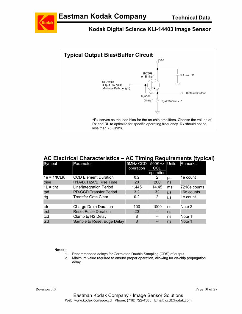
Typical Output Bias/Buffer Circuit
2N2369or Similar*
RX=180* RL=750 Ohms *
0.1 microF
To DeviceOutput Pin: VIDn(Minimize Path Length)
Buffered Output
VDD
Ohms
*Rx serves as the load bias for the on-chip amplifiers. Choose the values of Rx and RL to optimize for specific operating frequency. Rx should not be less than 75 Ohms.
Notes: 1. Recommended delays for Correlated Double Sampling (CDS) of output. 2. Minimum value required to ensure proper operation, allowing for on-chip propagation
delay.
AC Electrical Characteristics – AC Timing Requirements (typical) Symbol Parameter 5MHz CCD
operation 500KHz
CCD operation
Units Remarks
1e = 1/fCLK CCD Element Duration 0.2 2 µs 1e count trise H1A/B, H2A/B Rise Time 20 200 ns 1L = tint Line/Integration Period 1.445 14.45 ms 7218e countstpd PD-CCD Transfer Period 3.2 32 µs 16e counts ttg Transfer Gate Clear 0.2 2 µs 1e count tdr Charge Drain Duration 100 1000 ns Note 2 trst Reset Pulse Duration 20 -- ns tcd Clamp to H2 Delay 8 -- ns Note 1 tsd Sample to Reset Edge Delay 8 -- ns Note 1

Revision 3.0 Page 11 of 27 Eastman Kodak Company - Image Sensor Solutions
Web: www.kodak.com/go/ccd Phone: (716) 722-4385 Email: [email protected]
Eastman Kodak Company Technical Data
Kodak Digital Science KLI-14403 Image Sensor
Notes: 1. Care should be taken to insure that low rail overshoot does not exceed -0.5
VDC. Exceeding this value may result in non-photogenerated charged being injected into the video signal.
2. Connect pin to ground potential for applications where exposure control is not required.
Clock Line Capacitance Symbol Parameter Min. Nom. Max Units Notes CH1 Phase 1 Clock Capacitance -- 1940 -- pF 1 CH2 Phase 2 Clock Capacitance -- 2010 -- pF 1 CTG1 Transfer Gate 1 Capacitance -- 680 -- pF CPHIR Reset Gate Capacitance -- 12 -- pF CLOG Exposure Gate Capacitance -- 140 -- pF (1 of 3)
Notes: 1. This is the total load capacitance per CCD phase. Since the CCDs are driven from both
ends of the sensor, the effective load capacitance per drive pin is approximately half the value listed.
AC Electrical Characteristics – AC Timing Requirements Symbol Parameter Min. Nom. Max. VH1nH,VH2nH CCD Readout Clocks High 6.25 6.5 7.0 VH1nL,VH2nL CCD Readout Clocks Low -0.1 0.0 0.1 VTGnH Transfer Clocks High 6.25 6.5 7.0 VTGnL Transfer Clocks Low -0.1 0.0 0.1 VPHIRH Reset Clock High 6.25 6.5 7.0 VPHIRL Reset Clock Low -0.1 0.0 0.1 VLOGnH Exposure Clocks High 6.25 6.5 7.0 VLOGnL Exposure Clocks Low -0.1 0.0 0.1

Revision 3.0 Page 12 of 27 Eastman Kodak Company - Image Sensor Solutions
Web: www.kodak.com/go/ccd Phone: (716) 722-4385 Email: [email protected]
Eastman Kodak Company Technical Data
Kodak Digital Science KLI-14403 Image Sensor
Timing Diagram
7202e8e4e
7202e8e4e
H1n
H2n
TG2
Line Timing
LOGn
tint
tdr
Accumulation Gate-to-CCD Transfer Timing
H1n
H2n
1e
LOGn
tpd ttg
First Dark Reference Pixel Data Valid
8e
8e
2e
2e
7202e8e4e
7202e8e4e
8e
8e
2e
2e
texp
tdr
H2n
Output Timing
PHIR
VIDn
Clamp *
Sample *
tr
Vdark Vsat
trst tcd
tsd
H1n
1e
Vfeedthru
tclp
tspl
Even Output Odd Output
TG

Revision 3.0 Page 13 of 27 Eastman Kodak Company - Image Sensor Solutions
Web: www.kodak.com/go/ccd Phone: (716) 722-4385 Email: [email protected]
Eastman Kodak Company Technical Data
Kodak Digital Science KLI-14403 Image Sensor
KLI-14403 Functional Description Imaging During the integration period, an image is obtained by gathering electrons generated byphotons incident upon the photodiodes. The charge collected in the photodiode array is alinear function of the local exposure. The charge is stored adjacent the photodiode in theaccumulation region PHIA, and is isolated from the CCD shift registers during the integrationperiod by the transfer gates TGn, which are held at a barrier potential. At the end of a givenintegration period, the CCD register clocking is stopped with the H1 and H2 gates being heldin a 'high' and 'low' state respectively. Next, the TG gate is turned 'on' causing the charge todrain from the PHIÅ region, into the TG region. As the TG gate is turned to an 'off' state,charge is transferred into the H1 storage region, isolating the shift registers from the detectorregion once again. Complementary clocking of the H1 and H2 phases is then resumed forreadout of the current line of data while the next line of data is integrated. Separate TGgates are provided for each channel allowing for independent transfer to the shift register, foreach channel. However, the parallel connection of the shift register clocks requires thatH1/H2 clocking of all three channels be momentarily suspended, during the parallel transferfrom any channel photosites.
Charge Transport and Sensing Readout of the signal charge is accomplished by two-phase, complementary clocking of the H1 and H2 gates. The register architecture has been designed for high speed clocking with minimal transport and output signal degradation, while still maintaining low (6.25Vp-p min) clock swings for reduced power dissipation, lower clock noise and simpler driver design. The data in all registers is clocked simultaneously toward the output structures. The signal is then transferred to the output structures in a parallel format at the falling edge of the H2 clock. Re-settable floating diffusions are used for the charge-to-voltage conversion while source followers provide buffering to external connections. The potential change on the floating diffusion is dependent on the amount of signal charge and is given by dVFD = dQ/CFD. Prior to each pixel output, the floating diffusion is returned to the RD level by the reset clock, PHIR.

Revision 3.0 Page 14 of 27 Eastman Kodak Company - Image Sensor Solutions
Web: www.kodak.com/go/ccd Phone: (716) 722-4385 Email: [email protected]
Eastman Kodak Company Technical Data
Kodak Digital Science KLI-14403 Image Sensor
Typical Performance Measurements
KLI-14403 (monochrome)Typical Quantum Efficiency (%)
0%
10%
20%
30%
40%
50%
60%
70%
80%
90%
100%
350 450 550 650 750 850
Wavelength (nm)

Revision 3.0 Page 15 of 27 Eastman Kodak Company - Image Sensor Solutions
Web: www.kodak.com/go/ccd Phone: (716) 722-4385 Email: [email protected]
Eastman Kodak Company Technical Data
Kodak Digital Science KLI-14403 Image Sensor
KLI-14403 Reference Design The Kodak KLI-14403 Reference Design provides a baseline reference forthe design of a KLI-14403 image sensor into your electronic imaging application. The circuit below uses inexpensive off-the-shelf components to provide voltage-translated clock signals and DC bias supplies required to
MASTEROSCILLATOR
PLD
KLI-14403IMAGE SENSOR
+15 V
2N3904
180
750
.1
VoutRED
+ 15V
2N3904
180
750
.1
VoutGREE
+15 V
2N3904
180
750
.1
VoutBLUE
MPS3646
MPS5771
33
100K
100K
220p
F22
0pF
.1
1N914A
1N914A
1K
LOGB
LOGRLOGG
25
12
14
22
19
2
39
6
34
7
9
H1A
H2B
H2A
H1B
74ACT11244
IG SUB1,3,10,11,15,18,20,21,23,27,30,31,33
,37,38,4036
PHIR
1N914or
eqiv.1
10 uF .1 uF
18K
820
100 uF
Ferrite Bead
+ 15V
VSSR
VSSG
VSSB
VDD
RD
OG
26
29
28
13
17
24
16VIDG
VIDR
VIDB
10 K
.1
.1
.1
.1
2A12A22A32A4
1A11A21A31A4
1Y11Y21Y31Y4
2Y12Y22Y32Y4
1/G
2/G
2A12A22A32A4
1A11A21A31A4
1Y11Y21Y31Y4
2Y12Y22Y32Y4
1/G
2/G
+12.0V
+6.8 V
+6.8 V
+6.8 V
100
100
74ACT11244
EL7202
.1
.1
35 ID
Rd
Rd
Rd
Rd
.1
.1
LS8
TG+6.8 V EL7202
+6.8 V EL7202100
100
32
PHIA

Revision 3.0 Page 16 of 27 Eastman Kodak Company - Image Sensor Solutions
Web: www.kodak.com/go/ccd Phone: (716) 722-4385 Email: [email protected]
Eastman Kodak Company Technical Data
Kodak Digital Science KLI-14403 Image Sensor
Reference Design Circuit Overview Programmable Logic See the timing waveform requirements earlier in this document before programming a logic device. Clock Drivers There are three types of clock drivers (voltage translating buffers) used in thisreference design. The most important performance consideration is the ability of theclock driver to drive the capacitive loads presented by the various gates of the CCD. Reset Driver The RESET gate presents a small capacitive load of 100 pF, and requires fast riseand fall times. The complimentary bipolar switching transistor circuit shown aboveprovides a low cost solution. The circuit alternately drives the PNP and NPNtransistors into saturation, which switches the output between VCC and ground. A 33-ohm series damping resistor is used to suppress ringing.
Exposure Control and Transfer Gates The exposure control gates; LOGR, LOGG, and LOGB, and the transfer gate; TGeach present a moderate capacitive load of 500 pF. The Elantec 7202 Dual-ChannelPower MOSFET driver delivers a peak output current of 2 amperes - more thanenough to meet the rise and fall requirements of the LOG and TG gate. Seriesdamping resistors are used to prevent ringing in the LOG gates. The transfer gatesare connected together and driven by a single EL7202. CCD Shift Register Driver The CCD clock phases (H1A, H2A, H1B and H2B) present a significant load of 3100pF per phase. Two 74ACT11244 octal buffers provide an efficient solution. Eachclock phase is driven by four gates connected in parallel to increase output drivecurrent. The 6.5-volt swing required by the shift register is obtained by setting VCC to6.8 volts. Series damping resistors Rd are used to suppress ringing of the clocksignals. Values for Rd should be varied to eliminate ringing and achieve 50%crossover between each pair of shift register clocks.
Bias Supplies VDD, RD and OG VDD and VRD are supplied directly from the 15V input power supply and OG issupplied by a voltage divider. The input power should be sufficiently filtered to preventnoise from coupling into the output stage of the KLI-14403 through the VDD node.Current spikes in the VRD and VDD nodes, due to switching of the on-chip reset FET,are suppressed by the addition of a 0.1 uF decoupling capacitor to ground at eachnode. The decoupling capacitors should be located as close as possible to the pins ofthe CCD and should have a solid connection to ground. OG is also decoupled tosuppress voltage spikes the output gate of the device. The OG node draws negligiblecurrent.

Revision 3.0 Page 17 of 27 Eastman Kodak Company - Image Sensor Solutions
Web: www.kodak.com/go/ccd Phone: (716) 722-4385 Email: [email protected]
Eastman Kodak Company Technical Data
Kodak Digital Science KLI-14403 Image Sensor
OG,VSSR,VSSG,VSSB, PHIA A forward-biased diode provides an inexpensive and reliable voltage source for all three VSSnodes. The switching action of the reset FET of the output stage can cause voltage spikes tooccur on the VSS nodes. A decoupling capacitor located as close as practical to each VSSpin, and connected to a solid system ground, will minimize voltage spiking. In high dynamicrange systems, crosstalk between VSS channels might present a noise problem. A separatesupply for each of the three VSS nodes will minimize channel crosstalk if it proves to be aproblem.
Output Buffers An emitter follower circuit buffers each output channel. The emitter follower provides a highimpedance load to the on-chip source follower output stage, and provides low outputimpedance for driving the downstream analog signal processing circuits. A 180-ohm resistorconnected between the base and emitter of the emitter follower uses the forward biasedbase to emitter voltage drop to provide a constant current load for the on-chip output stage.

Revision 3.0 Page 18 of 27 Eastman Kodak Company - Image Sensor Solutions
Web: www.kodak.com/go/ccd Phone: (716) 722-4385 Email: [email protected]
Eastman Kodak Company Technical Data
Kodak Digital Science KLI-14403 Image Sensor
Package Configuration
For the serialized version, a non-sequential, non-repeating serial number will be written on the back of the package.

Revision 3.0 Page 19 of 27 Eastman Kodak Company - Image Sensor Solutions
Web: www.kodak.com/go/ccd Phone: (716) 722-4385 Email: [email protected]
Eastman Kodak Company Technical Data
Kodak Digital Science KLI-14403 Image Sensor Two-Sided Multilayer Anti-Reflective Cover Glass Specification (MAR)
Maximum Reflectance Allowed (two sided)
0.000.200.400.600.801.001.201.401.601.802.002.202.40
400 450 500 550 600 650 700
Wavelength (nm)
Ref
lect
ance
(%)
Reflectance (two sided)
Revision 3.0 Page 20 of 27 Eastman Kodak Company - Image Sensor Solutions
Web: www.kodak.com/go/ccd Phone: (716) 722-4385 Email: [email protected]
Eastman Kodak Company Technical Data
Kodak Digital Science KLI-14403 Image Sensor
General Device and Parameter Descriptions Charge Transfer Efficiency Charge Transfer Efficiency (CTE) is a measure of how efficiently electronic charge canbe transported by a Charge Coupled Device (CCD). This parameter is especiallyimportant in linear imager technology due to the fact that CCDs are often required totransport charge packets over long distances at very high speeds. The result of poorCTE is to reduce the overall MTF of the line image in a nonlinear fashion: the portion ofthe line image at the far end of the CCD will be degraded more than the image at theoutput end of the CCD, since it will undergo more CCD transfers. There are manypossible mechanisms that can negatively influence the CTE. Amongst thesemechanisms are included excessive CCD clocking frequency, insufficient drivepotential on the CCD clocking gates, and incorrect voltage bias on the output gate (OGsignal). The effect of these mechanisms is that some charge is "left behind" during aCCD transfer clocking cycle. Depending on the limiting mechanism, the lost chargecould be added to the immediate trailing cell or to a cell further back in time; thus,causing a horizontal smearing of the line image. The charge lost from a CCD cell, afterbeing transferred out of the CCD, is measured with respect to the original charge leveland is termed the charge transfer inefficiency (CTI). CTI is defined as
CTI =
Total Charge LostCharge Injected in each Pixel
×
1Number of CCD Transfers
.
The efficiency of the CCD transfer (CTE) is then defined as simply CTE = 1 − CTI, or
CTE = 1 −
Total Charge LostCharge Injected in each Pixel
×
1Number of CCD Transfers
.
Note that the total transfer efficiency for the entire line (TTE) is equal to (CTE)N, whereN is the total number of transfers which is equal to the number of phases per celltimes the number of cells (n). Dark Reference Pixels Dark reference pixels are groups of photosensitive pixels covered by a metal lightshield. These pixels are used as a black level reference for the image sensor output.Since the incident light is blocked from entering these pixels, the signal contained inthese pixels is due only to dark current. It is assumed that each photosensitive pixel(active and dark reference) will have approximately the same dark signal; thus,subtracting the average dark reference signal from each active pixel signal will removethe background dark signal level. Dark reference pixels are typically located at one orboth ends of the arrays, as shown earlier in this document for a linear image sensor inthe single channel schematic. Dark Signal Evaluation The dark signal evaluation measures the thermally generated electronic current (i.e.

Revision 3.0 Page 21 of 27 Eastman Kodak Company - Image Sensor Solutions
Web: www.kodak.com/go/ccd Phone: (716) 722-4385 Email: [email protected]
Eastman Kodak Company Technical Data
Kodak Digital Science KLI-14403 Image Sensor
background noise signal) at a specific operating temperature. Dark current ismeasured will all incident radiation removed (i.e. imager is in the dark). The currentmeasured by the picoammeter is the dark current of the photodiode array plus thedark current of the CCD array. Multiplying the dark current by the total integrationtime yields the quantity of dark charge. And dividing the dark current by the numberof photodiodes yields the dark current per photodiode (IDark). Dark voltage increaseslinearly with integration time, the worst case value occurs at the slowest clockingfrequency. Additionally, dark current doubles for approximately every 9°C increase intemperature. Dynamic Range Dynamic Range (DR) is the ratio of the maximum output signal, or saturation level, ofan image sensor to the dark noise level of the imager. The dark noise level, or noisefloor of an imager is typically expressed as the root mean square (rms) variation indark signal voltage. The dark signal includes components from dark current within thephotosite and CCD regions, reset transistor and output amplifier noise, and inputclocking noise. An input referred noise signal in the charge domain can be calculatedby dividing the dark noise voltage by the imager charge-to-voltage conversion factor.The dynamic range is typically expressed in units of decibels as: DR = 20 . LOG Exposure Control Exposure control is implemented by selectively clocking the LOG gates duringportions of the scanning line time. By applying a large enough positive bias to theLOG gate, the channel potential is increased to a level beyond the 'pinning level' ofthe photodiode. (The 'pinning' level is the maximum channel potential which thephotodiode can achieve and is fixed by the doping levels of the structure.) With TG inan 'off' state and LOG strongly biased, all of the photocurrent will be drawn off to theLS drain. Referring to the timing diagrams, one notes that the exposure can becontrolled by pulsing the LOG gate to a 'high' level while TG is turning 'off' and thenreturning the LOG gate to a 'low' bias level sometime during the line scan. Theeffective exposure (texp) is the net time between the falling edge of the LOG gate andthe falling edge of the TG gate (end of the line). Separate LOG connections for eachchannel are provided enabling on-chip light source and image spectral colorbalancing. As a cautionary note, the switching transients of the LOG gates during linereadout may inject an artifact at the sensor output. Rising edge artifacts can beavoided by switching LOG during the photodiode-to-CCD transfer period, preferably,during the TG falling edge. Depending on clocking speeds, the falling edge of theLOG should be synchronous with the H1/H2 shift register readout clocks. For veryfast applications, the falling edge of the LOG gate may be limited by on-chip RCdelays across the array. In this case artifacts may extend across one or more pixels.Correlated double sampling (CDS) processing of the output waveform can removethe first order magnitude of such artifacts. In high dynamic range applications, it maybe advisable to limit the LOG fall times to minimize the current transients in the devicesubstrate and limit the magnitude of the artifact to an acceptable level. Fixed Pattern Noise If the output of an image sensor under no illumination is viewed at high gain a distinctnon-uniform pattern, or fixed pattern noise, can be seen. This fixed pattern can be

Revision 3.0 Page 22 of 27 Eastman Kodak Company - Image Sensor Solutions
Web: www.kodak.com/go/ccd Phone: (716) 722-4385 Email: [email protected]
Eastman Kodak Company Technical Data
Kodak Digital Science KLI-14403 Image Sensor
removed from the video by subtracting the dark value of each pixel from the pixel values read out in all subsequent frames. Dark fixed pattern noise is usually caused by variations indark current across an imager, but can also be caused by input clocking signals abruptlystarting or stopping or by having the CCD clocks not being close compliments of each other.Mismatched CCD clocks can result in high instantaneous substrate currents, which whencombined with the fact that the silicon substrate has some non zero resistance can result inthe substrate potential bouncing. The pattern noise can also be seen when the imager isunder uniform illumination. An imager which exhibits a fixed pattern noise under uniformillumination and shows no pattern in the dark is said to have Light pattern noise orPhotosensitivity pattern noise. In addition to the reasons mentioned above, light patternnoise can be caused by the imager entering saturation, the nonuniform clipping effect of theantiblooming circuit, and by non-uniform, photosensitive pixel areas often caused by debris covering portions of some pixels. Imager Responsivity Responsivity is a measure of the imager output when exposed to a given optical energydensity. It is measured on monochrome and color (if applicable) versions of an imager overthe entire wavelength range of operation. Imagers having multiple photodiode arrays withdiffering color filters and/or photodiode dimensions have responsivity measured on eacharray Lag Lag, or decay lag is a measure of the amount of photogenerated charge left behind during a photodiode-to-CCD transfer cycle. Ideally, no charge is left behind during such transfersand lag is equal to zero; that is, 100% of the collected photogenerated charge is transferredto the adjacent CCD. The use of "pinned" photodiode technology enables the linearimagers to achieve near perfect lag performance. Improper Transfer Gate (TG) clockinglevels can introduce a lag type response. Thus, care must be taken to ensure that theclocking levels are not limiting the lag performance. Linearity The non-linearity of an image sensor is typically defined as the percent deviation from theideal linear response, which is defined by the line passing through Vsat and Vdark. Thepercent linearity is then 100 minus the non-linearity. The output linearity of a solid state image sensor is determined from the linearity of the photon collection process, the electronexposure structure nonlinearities (if it exists), the efficiency of charge transportation from thephotosite to the output amplifier, and the output amplifier linearity. The absorption ofphotons within the silicon substrate can be considered an ideal linear function of incidentillumination level when averaged over a given period of time. The existence of an electronic exposure control circuit adjacent to the photosensitive sites can introduce a non-linearity into the overall response by allowing small quantities of charge to remain isolated inunwanted potential wells. Whether or not any potential wells exist depends on the design and manufacturing of the particular image sensor. The existence of such potential wells inthe exposure circuitry, also called exposure defects, will degrade the linearity only at small

Revision 3.0 Page 23 of 27 Eastman Kodak Company - Image Sensor Solutions
Web: www.kodak.com/go/ccd Phone: (716) 722-4385 Email: [email protected]
Eastman Kodak Company Technical Data
Kodak Digital Science KLI-14403 Image Sensor
signal levels and may be different from one photosite to the next. An image sensor with excessive exposure defects would be rejected during quality assurance testing. The loss ofcharge during the transportation of charge packets from the photosite to the CCD, which istermed lag, tends to effect the linearity only at very small signal levels. "Pinned" photodiodes, or buried photodiodes, have extremely small lag (< 0.5%), and can beconsidered to be lag free. The CCD charge transfer inefficiency (CTI) will reduce theamplitude of the charge packet as it is transported towards the output amplifier, with the greatest effect realized at very small signal levels. Modern CCD's have CTE in excess of0.999999 per CCD transfer; thus, the overall effect on linearity is generally not a concern. Ifbiased properly, the output amplifier will yield a nonlinearity of typically less than 2%. Nonlinearity at signal levels beyond the saturation level is expected and can often varysignificantly from pixel to pixel. Linearity Evaluation Ideally, the output video amplitude should vary linearly with incident light intensity over the entire input range of irradiance. There are many possible phenomena which can causenon-linearity in the response curve; inadequate CTE and improper biasing or clocking toname a few. Electronic exposure control could be used to vary the photodiode integration time; however, since electronic exposure control can introduce non-linearity, it is not recommended as a method of input signal variation. The output signal versus relative irradiance is graphed and a least-squares, linear regression fit to the data is performed. The best-fit data curve should pass through zero volts and remain linear (R2 > 0.99) up to the Vsat level. Modulation Transfer Function (MTF) MTF is the magnitude of the spatial frequency response of a solid-state imager. The three main components of imager MTF are termed the aperture MTF, diffusion MTF, and chargetransfer efficiency MTF. The aperture MTF results from the discrete sampling nature of solidstate imagers, with smaller pixel pitches yielding a higher MTF response. The diffusion ofphotogenerated charge degrades the imager response and is responsible for the secondcomponent. The third component is due to inefficient charge transfer in the shift register.The maximum frequency an imager can detect without aliasing occurring is defined as theNyquist frequency and is equal to one over two times the pixel pitch. MTF is typicallyreported at the Nyquist frequency, 1/2 Nyquist, and 1/4 Nyquist. The aperture MTF limits themaximum response at Nyquist to 0.637 (Note that the maximum MTF response is 1.0). Thediffusion component will further degrade this value, especially at longer optical wavelengths. Noise Noise is any unwanted signal added to the imager output. Temporal noise sources present in a typical imager include the dark current, photon shot noise, reset transistor noise, CCDclocking noise, and the output amplifier noise. Dark current is dependent on the imageroperating temperature and can be reduced by cooling the imager. The reset transistor noise can be removed using correlated double sampling signal processing. The photon shot noisecannot be eliminated; however, by acquiring and averaging several frames it, and alltemporal noise sources, can be reduced. The variation in dark current from pixel to pixel

Revision 3.0 Page 24 of 27 Eastman Kodak Company - Image Sensor Solutions
Web: www.kodak.com/go/ccd Phone: (716) 722-4385 Email: [email protected]
Eastman Kodak Company Technical Data
Kodak Digital Science KLI-14403 Image Sensor leads to a dark noise pattern across an imager. The effects of this dark pattern noise can be
minimized by averaging several frames and then using the pixel-referenced, dark frame dataas the zero reference level for each pixel. Noise Evaluation The noise evaluation measures the noise levels associated with operating the imager at thespecified clocking speeds and temperatures. The test is performed with imager temperatureheld stable and all incident light is removed. The noise contributions of the evaluationcircuitry need to be removed from the calculation. Once this is done, the total imager noisewill be approximately equal to the sum of squares of each of the CCD clocking noise, outputamplifier noise, and the dark current noise. Photodiode Quantum Efficiency For a given area, absolute quantum efficiency is defined as the ratio of the number ofphotogenerated electrons captured during an integration period to the number of impingingphotons during that period. Higher values indicate a more efficient photon conversionprocess and hence are more desirable. Absolute photodiode quantum efficiency is calculated from the charge-to-voltage, imagerresponsivity, and measured active photodiode area. It's calculated over the entirewavelength range of operation and graphed on a curve as percent Quantum Efficiencyversus Wavelength. Given that the charge-to-voltage, responsivity, and active photodiode dimensions have allbeen measured, the absolute quantum efficiency can be calculated as
Quantum Efficiency (λ) = Responsivity (λ) Charge to Voltage ÷ Active Photodiode Area × Energy per Photon (λ)
÷
where Energy per Photon (λ) =
h . cλ and h . c = 1.98647E −25 [J−m]
Care should be taken to ensure that all quantities are represented in similar units before anycalculations are performed. Using the above formulas, the absolute quantum efficiency canbe expressed as
QE(λ) = 100% × R( λ) ÷ dV
dNe
÷ Are aDiode × hcλ .
Photoresponse Non-Uniformity (PRNU) The measurement is taken in a flat field white light. The intensity of the collimated light is setto a value approximately 10% to 20% below the saturated signal level. Depending on thewindowing length used, one region of pixels is observed for uniformity at a time. The averageresponse is calculated for each non-overlapping windowed section. In the case of medium orlow frequency PRNU measurements, a medium filter of 3-7 pixels is applied to this region toeliminate the effects of single point defects. The maximum and minimum pixel is determinedfor each windowed section. Again, for each section, the following formula is applied:

Revision 3.0 Page 25 of 27 Eastman Kodak Company - Image Sensor Solutions
Web: www.kodak.com/go/ccd Phone: (716) 722-4385 Email: [email protected]
Eastman Kodak Company Technical Data
Kodak Digital Science KLI-14403 Image Sensor
PRNU = 100% ×
(Maximum_Pixel_Value − Minimum_Pixel_Value )Mean_Pixel_Value .
Each section is then compared against the specification to identify the region with the largest percent deviation from the average response for the imager. Resolution The resolution of a solid state image sensor is the spatial resolving power of that sensor. Thespatial resolution of a sensor is descried in the spatial frequency domain by plotting themodulation transfer function (MTF) versus spatial frequency. The discrete sampling nature ofsolid state image sensors gives rise to a sampling frequency which will determine the upper limitof the sensor's frequency response. Resolution is frequently described in terms of the number ofdots or photosites per inch (DPI) in the imager or object planes. For example, a linear imagesensor with a single array of 1000 photosites of pitch 10 µm would have a resolution of 2540DPI (1000 / (1000 x .01mm x 1"/25.4mm)). If the sensor is used in an optical system to imagean 8" wide document, then the resolution in the document plane would be 125 DPI (1000 pixels/ 8"). This example is slightly misleading in that it does not consider the frequency response ofthe sensor or the optics. In reality, the sensor will have an MTF of between 0.2 and 0.7 at theNyquist spatial frequency and the optics are likely to have an MTF of 0.6 to 0.9 at the Nyquistfrequency. It is important to note that even though a sensor may have a high enough samplingfrequency for a particular application, the overall frequency response of the sensor and opticsmay not be sufficient for the application! Saturation Voltage The saturated signal level is the output voltage corresponding to the maximum charge packetthe imager can handle. Adding charge above the saturated level results in the excess charge"spilling" over into neighboring photosites or CCD structures. Either the photodiode capacity orthe CCD capacity, with the latter being the most typical case can limit the charge capacity. Thesaturated signal level is measured by monitoring the dark-to-light transition between the first-outdark reference pixels and the first active pixels while the irradiance is slowly increased. Notethat improper settings on either the output gate (OG) or the reset gate (PHIR) can have aclipping effect on the output waveform. Smear Smear, also referred to as Photodiode-to-CCD Crosstalk, occurs when photogenerated chargediffuses to an adjacent CCD and is collected, as opposed to being collected in the photodiodewhere the photon absorption occurred. The result of smear is to increase the backgroundsignal within the dark reference pixels and CCD buffer pixels. This increased background signalreduces the achievable dynamic range; hence, a high smear value is undesirable. The furtherthe photodiode array and the CCD are apart, the less the smear. Contributors to increasedsmear are a short photodiode-to-CCD separation and improper transfer gate clocking levels ortiming. Smear is also highly dependent on incident photon wavelength. In the application, anIR cut-off filter (~710nm) is recommended.

Revision 3.0 Page 26 of 27 Eastman Kodak Company - Image Sensor Solutions
Web: www.kodak.com/go/ccd Phone: (716) 722-4385 Email: [email protected]
Eastman Kodak Company Technical Data
Kodak Digital Science KLI-14403 Image Sensor
Quality and Reliability • Quality Strategy: All devices will conform to the maximum and minimum specifications stated
in this document. This is accomplished through a combination of statistical process control and inspection at key points of the production process. Typical specification limits are notguaranteed but provided as a design target.
• Replacement: All devices are warranted against failures in accordance with the Terms ofSale.
• Cleanliness: Devices are shipped free of mobile contamination inside the package cavity.Immovable particles and scratches that are within the imager pixel area and the correspondingcover glass region directly above the pixel sites are also not allowed. The cover glass is highly susceptible to particles and other contamination. Touching the cover glass must be avoided.See ISS Application Note DS 00-009, Cover Glass Cleaning, for further information.
• Mechanical: Device assembly drawing is provided as a reference. The device will conform to the published package tolerances.
• ESD Precautions: Devices are shipped in static-safe containers and should only be handled at static-safe workstations.
• Reliability: Information concerning the quality assurance and reliability testing procedures and results are available from the Image Sensor Solutions, and can be supplied upon request.
• Test Data Retention: Devices have an identifying number traceable to a test data file. Testdata is kept for a period of 2 years after date of shipment.
Ordering Information Contact the Eastman Kodak Company for more information.
Address all inquiries and purchase orders to: Image Sensor Solutions Eastman Kodak Company Rochester, New York 14650-2010 Phone: (716) 722-4385 Fax: (716) 477-4947 Email: [email protected] Web: www.kodak.com/go/ccd
Kodak reserves the right to change any information contained herein without notice. All informationfurnished by Kodak is believed to be accurate.
WARNING: LIFE SUPPORT APPLICATIONS POLICY Image Sensor Solutions, Eastman Kodak Company products are not authorized for and should notbe used within Life Support Systems without the specific written consent of the Eastman KodakCompany. Product warranty is limited to replacement of defective components and does not coverinjury to persons or property or other consequential damages.

Revision 3.0 Page 27 of 27 Eastman Kodak Company - Image Sensor Solutions
Web: www.kodak.com/go/ccd Phone: (716) 722-4385 Email: [email protected]
Eastman Kodak Company Technical Data
Kodak Digital Science KLI-14403 Image Sensor Revision Changes Revision Number Description of Change
3.0 AC Electrical Characteristics – AC Timing Requirements table on page 10 corrected and updated for 5MHz and 500KHz operation. Eliminate reference to Color Filter Type II on page 7 – now only one type of filter.