eb47 - ispmach 4000ze pico development kit user's guide
TRANSCRIPT

September 2009Revision: EB47_01.0
ispMACH 4000ZE Pico Development Kit
User’s Guide

2
ispMACH 4000ZE Pico Development KitLattice Semiconductor User’s Guide
IntroductionThank you for choosing the Lattice Semiconductor ispMACH® 4000ZE Pico Development Kit!
This user’s guide describes how to start using the ispMACH 4000ZE Pico Development Kit, an easy-to-use plat-form for evaluating and designing with the LC4256ZE CPLD. Along with the evaluation board and accessories, this kit includes a pre-loaded Pico Power demonstration design. You may also reprogram the on-board LC4256ZE and ispPAC®-POWR6AT6 devices to review your own custom designs.
Note: Static electricity can severely shorten the lifespan of electronic components. See the ispMACH 4000ZE Pico Development Kit QuickSTART Guide for handling and storage tips.
FeaturesThe ispMACH 4000ZE Pico Development Kit includes:
• ispMACH 4000ZE Pico Evaluation Board - The Pico board is a 2.5” x 2” form factor that features the following on-board components and circuits:
– ispMACH 4256ZE CPLD (LC4256ZE-5MN144C)– Power Manager II ispPAC-POWR6AT6 mixed-signal PLD (ispPAC-POWR6AT6-01NN32I)– High-side current sensor circuits– Battery or USB power– LCD panel– USB B-mini connector for power and programming– 15x2 expansion header landing for general IO, I2C, and JTAG– Keyboard-style DIP switch bank– Push-button input– 3.3V and 1.8V supply rails– Optional battery recharge circuit
• Pre-loaded Pico Power Demo – The kit includes a pre-loaded demo design that highlights key CPLD applica-tions and power-saving design methods that maximize battery life.
• USB Connector Cable – The Pico board is powered from the mini B USB socket when connected to a host PC. The USB channel also provides a programming interface to the LC4256ZE and POWR6AT6 JTAG ports.
• QuickSTART Guide – Provides information on connecting the Pico board, running the pre-loaded Pico Power demo.
• ispMACH 4000ZE Pico Development Kit Web Page – The ispMACH 4000ZE Pico Development Kit web page (www.latticesemi.com/4000ze-pico-kit) provides access to the latest documentation (including this guide), demo designs, and drivers for the kit.
The contents of this user’s guide include demo operation, programming instructions, top-level functional descrip-tions of the evaluation board, descriptions of the on-board connectors, switches and a complete set of schematics of the Pico board.

3
ispMACH 4000ZE Pico Development KitLattice Semiconductor User’s Guide
Figure 1. Pico Evaluation Board, Top Side
Figure 2. Pico Evaluation Board, Bottom Side

4
ispMACH 4000ZE Pico Development KitLattice Semiconductor User’s Guide
Software RequirementsInstall the following software before you begin developing designs for the evaluation board:
• ispLEVER® Classic 1.3 (ispMACH 4000ZE CPLD support)
• PAC-Designer® 5.1 (ispPAC-POWR6AT6 mixed-signal PLD support)
• ispVM™ System 17.5 (Required for re-programming on-board PLDs)
• PicoView 1.04 (Required for the I2C GPIO Expansion Demo)
ispMACH 4000ZE DeviceThis board features the ispMACH 4000ZE CPLD which is ideal for ultra low-power, high-volume portable applica-tions. The on-board LC4256ZE is the highest capacity of the family with 256 macrocells. The 144-pin csBGA pack-age provides 108 user I/Os and four dedicated inputs in a 7mm x 7mm package. The LC4256ZE consumes standby current as low as 15µA. A complete description of this device can be found in the ispMACH 4000ZE Family Data Sheet.
Demonstration DesignsLattice provides two demos that illustrate key applications of the ispMACH 4000ZE CPLD device in the context of a consumer electronics application:
• Pico Power – Integrates an up/down counter, a right/left shift register, voltage/current meter display, and an I2C bus master controller that communicates with the on-board POWR6AT6 Power Manager II device. The POWR6AT6 provides analog power supply monitoring and a 2-wire I2C interface to measure various voltage sup-plies of the board. An LCD panel displays demo output using three characters. You can select demo features with the keyboard-style 4-bit DIP switch bank. The Pico Power demo is designed for battery operation but if one isn’t available you can power the board by connecting the USB cable provided to a PC USB port.
• GPIO I2C Expansion – Shows an application of the LC4256ZE device as an I2C slave processing instructions issued by a CPU/MPU. CPLDs are ideal GPIO “expanders” for processors. Control registers of the CPLD’s I2C module allow the processor to access counter and shift registers, I/O, and power measurements. An I2C software interface utility, PicoView, emulates the CPU/MPU component of the system. Visit www.latticesemi.com/4000ze-pico-kit to download PicoView.
Note: It is possible that you will obtain your Pico board after it has been reprogrammed. To restore the factory default demo and program it with other Lattice-supplied examples, see the Download Demo Designs section of this document.
Pico Power DemoThe Pico Power design highlights low-power features of the LC4256ZE CPLD along with inexpensive PCB design techniques that help extend battery life, such as low-speed CPLD clocking, efficient use of the CPLD I/O cell’s I/O bus maintenance feature, and gated supply rails. The demo design integrates an I2C master reference design (www.latticesemi.com/products/intellectualproperty) with LCD controller logic, an up/down counter and left/right shift register modules. You may switch the LCD display between a current/voltage meter and counter/shifter opera-tion using the DIP switch bank. The demo shows a clock generator based on the LC4256ZE on-chip oscillator and timer (OSCTIMER) hardware feature. The counter and shift register modules can be clocked at either <2 Hz or 5 MHz to help illustrate the difference in dynamic power demands.
Current and voltage monitoring of the Pico board is provided by the POWR6AT6 mixed-signal PLD and on-board sensor circuits (see AN6049, High-side Current Sensing Techniques for Power Manager Devices). To minimize power consumption of the overall system, the POWR6AT6 supply rail is powered on momentarily by the LC4256ZE whenever a current or voltage display is requested or after the Pico board is reset.

5
ispMACH 4000ZE Pico Development KitLattice Semiconductor User’s Guide
Figure 3. Pico Power Demo Block Diagram
4-bit DIP Switch
4
Right/LeftShift Register
I2CMaster
InputControl
3-char 7-seg LCD
ispMACH 4256ZE
ispPAC-POWR6AT6
VMON1 – Core Current VMON2 – I/O Current VMON3 – Spare 1 VMON4 – Spare 2 VMON5 – 5V USB VMON6 – 3V Battery
ADC
I2C Slave
Up/DownCounter
VMON4
I2C
ClockGenerator
5 MHz < 2 Hz
POWR6AT6 Enable
POWR6AT6 Supply
The following tables describe the 4-bit DIP switch and push-button inputs that control the pre-configured Pico Power demo. Use them as a reference for the procedure you must follow in the next step. A switch in the raised position of the 4-bit DIP switch indicates a logic level ‘1’ input to the LC4256ZE. Depress a switch to indicate a low logic level ‘0’.
Figure 4. Pico Board with 4-Bit DIP Switch Example (1010)

Switch 1234 (Demo) Pico Power Demo Features
0000 (Up)0001 (Down)
Decimal Up/Down Counter Display – Displays an 8-bit decimal up/down counter (0.0-9.9) using the <2 Hz clock generated by the LC4256ZE On-Chip Oscillator and Timer (OSCTIMER). A 4-bit nibble is committed to the “ones” and “tenths” position of the LCD. The down counter will be initial-ized to 9.9 and up counter to 0.0 upon power-up, reset or if the count rolls over.
Slow clock <2 Hz:1100 (VMON1 Icccore)1001 (VMON2 Iccio)
Fast Clock 5 MHz:1000 (VMON1 Icccore)
Current Meter Display – Displays current measurements of the LC4256ZE 1.8V core and 2.5V I/O supply rails. To help illustrate the relative dynamic power requirements of the board at <2 Hz or 5 MHz, Icccore can be measured at both clock frequencies.
The current meter circuit includes a high-side current sensor amp and the POWR6AT6 mixed-sig-nal PLD which provides the voltage monitor, analog-to-digital conversion (ADC), and an I2C slave to register the measurement. The entire circuit is dynamically energized whenever the current meter function is selected or the Pico board push-button is pressed. Note that the additional draw of the meter circuit is factored into the display latched into the LCD panel by the CPLD. This will result in an additional 100-600 microamp over static measurements taken on the board at the Icccore and Iccio shunts R35 and R34.
0010 (Shift Left)0011 (Shift Right)
Left/Right Shift Register Display – Displays a shift register operating as serial-in, parallel-out using the <2 Hz clock source. Each bit of the register is associated with the corresponding seg-ment of the 7-segment LCD such that reg(21) = Segment 7 of the left-most character and reg(0) = Segment 1 of the right-most character.
When shifting left, the register will shift in ‘0’ to the MSB upon each clock. When shifting right the register shifts in ‘0’ to the LSB. The shift register will be initialized to 1FFFFEh upon power-up, reset, or if the shift result rolls over.
1010 (VMON5 5V USB)1011 (VMON6 3V Battery)
Volt Meter – Displays voltage measurements of the 5V USB interface or the 3V button-cell battery. The volt meter function dynamically activates the POWR6AT6 supply rail in the same manner as the Current Meter Display function.
1111 (Standby) Standby Mode (Default) – Demonstrates standby power of the LC4256ZE. No LCD output is available in this mode.
In battery-powered, standby mode CPLD core current draw is ~10µA.
Other Reserved switch settings. No LCD output.
Push Button Switch Pico Power Demo Feature
SW1 Manual Reset is a push-button switch (SW1) used to assert a manual reset of the demo. All design modules including the CPLD OSCTIMER will be initialized when SW1 is pressed.
6
ispMACH 4000ZE Pico Development KitLattice Semiconductor User’s Guide
Run the Pico Power DemoFollow the procedure below to explore the Pico Power demonstration on the evaluation board.
1. Select Switch Bank pattern 1111 (Standby)The Pico board activates the LC4256ZE standby mode. To measure the current draw of the CPLD core (Icccore), touch voltmeter leads across R35, read the voltage drop, and then divide by 50 Ohms (I=V/R). The LC4256ZE draws approximately 10µA in Standby mode. Given a new button-cell battery the Pico board should be operational for approximately one year in standby mode. As a further measure to minimize CPLD current draw, I/O Bus Maintenance features are disabled and the DIP switch input is designed to pull input high rather than open, high-Z. This will avoid current leakage by the CPLD buffers by disabling the internal pull-down resis-tor circuits.
2. Select Switch Bank pattern 1100 (Low-speed CPLD core current meter)The LCD displays CPLD core current (Icccore) in microamp (µA) units. The CPLD control logic performs the following operations to arrive at the result. First, the counter and the shift register modules of the CPLD are enabled by the internal slow clock (<2Hz) and the ispPAC-POWR6AT6 power supply rail is enabled. Next, the I2C master module issues three I2C bus cycles to initiate and read the analog-to-digital conversion result of the POWR6AT6 voltage monitor input (VMON1). Finally, the data is displayed on the LCD in microamp units. The POWR6AT6 VMON1 is driven by a high-side current sense circuit connected to the CPLD Vcccore supply rail. Power consumption of the CPLD in the slow speed operation is in the µA range. Note that a volt meter reading across R35 will reflect current draw after the POWR6AT6 has powered off and therefore be 100-600 micro-amps less than the value latched by the CPLD.

7
ispMACH 4000ZE Pico Development KitLattice Semiconductor User’s Guide
3. Select Switch bank pattern 0000 (decimal up counter).The LCD displays a decimal up-counter. The counter uses a divided OSCTIMER clock source set for 5 kHz nominal (TIMER_DIV=1024). 5 kHz is further divided to produce a count frequency of < 2 Hz. Use the voltme-ter technique in step 1 to measure core current.
4. Select Switch bank pattern 1000 (CPLD core current meter).The LCD displays the VMON1 Icccore in µA units as the CPLD OSCTIMER clocks the counter and shift regis-ter design modules at 5 MHz and the LCD at < 2 Hz. At this higher frequency the core current increases.
5. Select Switch bank pattern 0010 (left shift).The LCD displays the 21-bit shift register module operating on each segment at < 2 Hz.
6. Experiment with other functions and measurements of the Pico Power Demo. If the Pico board battery is missing you may connect the Pico board to a USB socket with the cable provided to enable the USB 5V supply rail.
I2C GPIO Expansion DemoThis demo illustrates I2C traffic between a PC host running the I2C Hardware Verification Utility program (PicoView) and the Pico board. Data is available at the expansion header landing or LCD display. Control and status registers of the I2C master and slave modules can be read or written via the PicoView user interface. These instructions highlight the LC4256ZE, providing general-purpose I/O for an I/O-constrained microprocessor.
Figure 5. GPIO I2C Expansion Demo
4-bit DIP Switch
15X2Header
I2C Address
8
4
Counter
ShiftRegister
POWR6AT6 Register
GeneralPurpose I/O
DIP Switch
3-char 7-seg LCD
24
LampTest
ispMACH4256ZE
ispPAC-POWR6AT6
ADC
I2C Slave
I2C Slave
Trim Cells
ControlLogic
6
I2C Address
VMON6
Processor (PicoView)
2
I2C over USB
I2C Address RO
ControlRegisterR/W
CounterRegister
POWR6AT6 Register
GeneralPurpose I/O
DIP Switch
R/W
WO
R/W
RO
15X2Header
VMON[1-6]RO
POWR6AT6 I2C Address
I2C Master
ShiftRegisterR/W
ispMACH 4256ZE
ispPAC-POWR6AT6
R/W
15X2Header
VMON1 – Core Current VMON2 – I/O Current VMON3 – Spare 1 VMON4 – Spare 2 VMON5 – 5V USB VMON6 – 3V Battery
8
ispMACH 4000ZE Pico Development KitLattice Semiconductor User’s Guide
Download PicoView Software and I2C GPIO Expansion DemoThe following steps require a host PC with a USB port configured to communicate with the Pico board. Before you begin, you will need to obtain the I2C interface program, PicoView, and the I2C GPIO Expansion demo design, from the Lattice web site.
1. Browse to www.latticesemi.com/4000ze-pico-kit.
2. Select the PicoView for Windows Software download, review the software license agreement, save the ZIP file to your system, and unzip it to a location on your PC. For example: c:\4000ze-pico-kit. The ZIP archive contains picoview.exe.
3. Select the I2C GPIO Expansion Demo download, save the ZIP file to your system, and unzip it to a location on your PC. For example: c:\4000ze-pico-kit.
Connect to the Pico Evaluation BoardIn this step, connect the evaluation board to your PC using the USB cable provided. Once connected you can use ispVM System software to reprogram the Pico board or use PicoView software to interact with the interface regis-ters of the I2C GPIO Expansion demo.
Connect one USB cable from a USB port on your PC to the board’s USB-to-I2C interface socket on the side of the board as shown in the PCB diagram. After connection is made, a blue Power LED will light up indicating the board power is now supplied from the USB cable.
Reprogram the Pico Evaluation BoardThe Power demo design is pre-programmed into the Pico board by Lattice. To program the Pico board with the I2C GPIO Expansion Design, use ispVM System software. This step requires that ispVM System be installed. For more information see www.latticesemi.com/products/designsoftware/ispvmsystem.
1. If not already connected, follow the procedure above to connect the Pico board and install hardware drivers. The USB cable must be attached and powered to enable the Pico board I2C channel and JTAG programming interface.
2. From the Start menu run ispVM System. ispVM appears.
3. Choose Options > Cable and IO Port Setup... The Cable and I/O Port Setup dialog appears.
4. Specify the following:
Cable Type: USB2Port Setting: FTUSB-0Click OK
5. The New Scan Configuration Setup window appears. The LC4256ZE appears in the device list.
6. Right-click the LC4256ZE entry and choose Edit Device... The Device Information dialog appears.
7. From the Data File section, click the Browse button. The Open Data File dialog appears.
8. Browse to the c:\4000ze-pico-kit\gpio-demo folder, select gpio-demo.jed, and click Open. From the Opera-tion list choose Erase, Program, Verify and click OK.
9. Right-click the ispPAC-POWR6AT6 row, from the Set Device Operations menu, choose Bypass.
10. Choose Project > Download. ispVM reprograms the Pico board. Programming requires about 20-40 seconds. A small timer window will appear to show elapsed programming time. At the end of programming, the configu-ration setup window should show a PASS in the Status column.

9
ispMACH 4000ZE Pico Development KitLattice Semiconductor User’s Guide
Run the I2C GPIO Expansion DemoThese instructions highlight the LC4256ZE providing general-purpose I/O for an I/O-constrained microprocessor or DSP. A host PC running the Lattice PicoView program emulates a processor reading and writing I2C traffic to I2C slaves embedded in the LC4256ZE and POWR6AT6 devices. The CPLD integrates Verilog-based I2C slave and LCD Controller reference designs to translate the traffic to parallel interfaces of the Pico board. The I2C interface to the POWR6AT6 allows you to monitor voltage or current of various Pico board power supplies.
1. If not already connected, follow the earlier procedures to connect the Pico board and reprogram it. The USB cable must be attached and powered to enable the Pico board I2C channel and JTAG programming interface.
2. Start a command prompt and run the PicoView program (c:\4000ze-pico-kit\picoview.exe).PicoView provides a push-button interface to provide read or read/write access to the registers of the LC4256ZE and POWR6AT6 devices. When PicoView initializes, all device registers are read and the dialog is refreshed. A column of “R” and “W” buttons provide read or read/write control over individual registers of the LC4256ZE. See Figure 5 for details.
3. Choose Options > Control Register. The Control Register dialog appears.
4. From the Counter/Shift Control section of the dialog select Count Down/Shift Right, from the LCD Display section, select Shift Register, and then click OK. The Control Register box is updated with value 0x14h.
5. Click the Control Register W button. PicoView writes the control settings to the Pico board to initiate the embedded shift register and display the results to the LCD panel.
6. From the ispPAC-POWR6AT6 section of the dialog, select VMON1 – Core Current and click the Read button. PicoView updates the POWR6AT6 Register with the core current in microamp units.
Figure 6. PicoView Screen Shot

10
ispMACH 4000ZE Pico Development KitLattice Semiconductor User’s Guide
Hardware EvaluationHow to evaluate hardware features of the on-board LC4256ZE.
Power ConsumptionTables 1 and 2 list a series of measurements for the CPLD I/O and core current running the Pico Power demonstra-tion design when powered by battery or the USB cable interface.
CPLD power consumption can be measured by the on-board sensor circuits or by metering across resistors R34 (I/O, 100 ohm) and R35 (Core, 50 ohm) of the Pico board (see Figure 2). Use Ohm’s Law to calculate current from the voltage drop across each resistor: I = V / R.
Note that voltmeter measurements reflect a lower static current level than what the on-board meter and PicoView results display which accounts for the additional current that occurs when the POWR6AT6, current sense amplifi-ers, and switch circuits are dynamically powered for a measurement.
The board will draw additional current when USB power is applied due to the LC4256ZE JTAG and I/O pins being biased from surrounding USB support circuits. When powered by the battery cell, the LC4256ZE pins are isolated by high-impedance circuits to minimize current leakage paths.
Table 1.
Feature
Static Dynamic
I/OCurrent
CoreCurrent
Pico Board (LCD)
Counter0000 - Decimal Up
0001 - Decimal Down
Current Meter
1000 - CPLD Core (5 MHz)
1100 - CPLD Core
1001 - CPLD I/O
Shift0010 - Left
0011 - Right
Voltage Meter
1010 - USB 5V
1011 - Battery 3V
Standby 1111
Sample Current and Voltage Measurements – Battery Power
Table 2.
Feature
Static Dynamic
I/OCurrent
CoreCurrent
Pico Board (LCD)
PicoView
I/OCurrent
CoreCurrent
Counter0000 - Decimal Up
0001 - Decimal Down
CurrentMeter
1000 - CPLD Core (5 MHz)
1100 - CPLD Core
1001 - CPLD I/O
Shift0010 - Left
0011 - Right
Voltage Meter
1010 - USB 5V
1011 - Battery 3V
Standby 1111
Sample Current and Voltage Measurements - USB Power
0µA 390µA N/A
1µA
624µA 768µA
490µA704µA
688uA (I/O)
390µA N/A
490µA0V
2.88V
10µA N/A
626uA
624µA
N/A 772µA636µA
N/A750µA
768µA (Core) 784µA
690µA688µA (Core)
740µA682µA
800µA (I/O) 693µA
624µAN/A
781µA 640µAN/A
690µA4.96V
751µA685µA
2.78V
450µA N/A 450µA

11
ispMACH 4000ZE Pico Development KitLattice Semiconductor User’s Guide
Download Demo DesignsThe Pico Power demo is preprogrammed into the Pico board, however over time it is likely your board will be modi-fied. Lattice distributes source and programming files for demonstration designs compatible with the Pico board.
To download demo designs:
1. Browse to the ispMACH 4000ZE Pico Development Kit web page (www.latticesemi.com/4000ze-pico-kit) of the Lattice web site. Select the Demo Applications download and save the file.
2. Extract the contents of Pico_DK_DemoSource.zip to an accessible location on your hard drive. Three demo design directories (Demo_<device>_<demo>) are unpacked.
Demo Directory
Pico Power
picopower-demo.\project.\source.\testbench
I2C GPIO Expansion
gpio-demo .\project.\source.\testbench
Both supplymonitor-demo.\project
Where:
• .\project – ispLEVER Classic project (.syn) or PAC-Designer project (.pac) and programming file (.jed). This directory may contain intermediate results of the ispLEVER Classic or PAC-Designer compile process.
• .\source – HDL source files for the ispLEVER Classic project.
• .\testbench – HDL test fixture for the ispLEVER Classic project.
Recompile a LC4256ZE Demo Project with ispLEVER ClassicUse the procedure described below to recompile any of the LC4256ZE demo projects for the Pico Evaluation Board.
1. Install and license ispLEVER Classic software.
2. Download the demo source files from the ispMACH 4000ZE Pico Development Kit web page.
3. Run the ispLEVER Classic Project Navigator.
4. Open the <demo>.syn project file.
5. From the Source in project window, select the target device. The Fit Design process appears in the Processes for current source window.
6. Select Fit Design, right-click and choose, Start. After a few moments the JEDEC programming file is output.
7. See the Programming with ispVM section of this document for details on downloading a programming file to the board.
Recompile a POWR6AT6 Demo Project with PAC-DesignerUse the procedure described below to recompile any POWR6AT6 demo project for the Pico Evaluation Board. The POWR6AT6 has limited I/O access so trim output features are limited. The only programmable option that can be modified is the I2C address.

12
ispMACH 4000ZE Pico Development KitLattice Semiconductor User’s Guide
1. Install and license PAC-Designer software
2. Download the demo source files from the ispMACH 4000ZE Pico Development Kit web page.
3. Run PAC-Designer.
4. Open the <demo>.pac project file.
5. Choose File > Export… The Export dialog appears.
6. Select Export What: Jedec File.
7. Click the Browse… button. The Save As dialog appears.
8. Browse to the destination folder, specify a file name, and click Save.
9. Click OK. After a few moments the JEDEC programming file is output.
10. See the Programming with ispVM Section of this document for details on downloading a programming file to the board.
Programming with ispVMThe Pico Power demo design is pre-programmed into the Pico board by Lattice. To restore a Pico board to factory settings or load an alternative demo design, use the procedures in this section.
To install ispVM programming tools:
1. Install and license ispVM System software.
2. Connect the board to a host PC using the USB port header connection.
3. Follow the USB Cable Interface procedure below to program the evaluation board.
USB Cable InterfaceThe Pico board is equipped with a built-in USB-based programming circuit. This consists of a USB PHY and a USB connector. When the board is connected to a PC with a USB cable, it is recognized by the ispVM System software as a “USB Download Cable”. The LC4256ZE and POWR6AT6 can then be scanned and programmed using the ispVM System software.
To program a demo programming file:
1. From the Start menu run ispVM System. ispVM appears.
2. Choose Options > Cable and IO Port Setup…The Cable and I/O Port Setup dialog appears.
3. Make the following selections:
Cable Type: USB2Port Setting: FTUSBClick OK
4. Choose ispTools > Scan Chain. The New Scan Configuration Setup window appears. The LC4256ZE and POWR6AT6 device(s) appear in the device list.
5. Right-click the LC4256ZE or ispPAC-POWR6AT6 entry and choose Edit Device… The Device Information dialog appears.
6. From the Data File section, click the Browse button. The Open Data File dialog appears.

13
ispMACH 4000ZE Pico Development KitLattice Semiconductor User’s Guide
7. Browse to the <Demo Dir>\project folder, select <Demo>.jed, and click Open. From the Operation list choose Erase, Program, Verify and click OK.
Optional: Choose the Bypass operation for devices in the scan chain that don’t require re-programming.
8. Choose Project > Download. ispVM reprograms the evaluation board.
Programming requires about 20-40 seconds. A small, timer window will appear to show elapsed programming time. At the end of programming, the configuration setup window should show a PASS in the Status column.
PicoView SoftwareThis section describes the features of the PicoView for Windows software program.
ConceptsPicoView provides an easy-to-use interface to the I2C control and status registers within the GPIO I2C Expansion demo design. PicoView communicates between a Windows PC and the Pico board using an I2C-over-USB connec-tion.
PicoView issues I2C commands just as would an I2C master controller. You can view, and in many cases preload, control registers prior to issuing a read or write command. To help understand the register set of the demo, see the I2C GPIO Expansion Demo section and Figure 5 for more information.
ProceduresThis section describes how to navigate the PicoView user interface.
Running PicoViewTo run PicoView:
1. See the connection and programming procedure for the GPIO I2C Expansion demo to prepare the Pico board.
2. Download PicoView from www.latticesemi.com/4000ze-pico-kit and unzip the archive file. Picoview.exe is unpacked.
3. From a Windows command prompt run: <install>\Picoview.exe.
SetupBy default, PicoView is set to communicate between a PC and the Pico board over a USB cable. PicoView can also be set up to operate in a demo mode without hardware. See the PicoView I2C Settings dialog for more information.
I2C Command ExecutionTo execute an I2C command:
1. From the PicoView Window, click a Control Register Button. A control register dialog box appears. A variety of dialog styles are available depending on the register. See the User Interface section below for details.
2. Set the register options and click OK. The PicoView user interface will refresh with the updated register com-mand in hex format.
3. Click the R (read) and W (write) buttons to update the register of the related I2C slave/peripheral register. The PicoView user interface will refresh the status registers. In some cases the Pico board’s LCD operation will change.
See the Run the I2C GPIO Expansion Demo section of this document for a PicoView operation example.
User InterfaceThis section describes elements contained within the PicoView graphical user interface. These elements include windows, menus, toolbars, and dialog boxes.

14
ispMACH 4000ZE Pico Development KitLattice Semiconductor User’s Guide
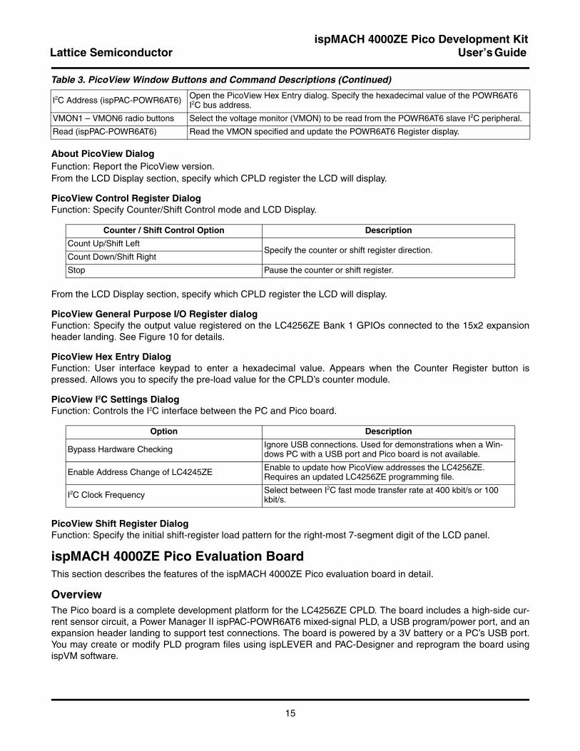
PicoView WindowThe PicoView window provides access to control and status registers and a series or read or write actions that can be issued by the I2C bus master module emulated by PicoView.
Figure 7. PicoView Window
Table 3. PicoView Window Buttons and Command Descriptions
Control Buttons Button or I2C Master Command Description
I2C Address (ispMACH 4256ZE) Open the PicoView Hex Entry dialog. Specify the hexadecimal value of the LC4256ZE CPLD I2C bus address.
Control Register [R|W]Open the PicoView Control Register dialog.R – Read the current control register value and update the Control Register button display.W – Write the current control register commands to the I2C slave peripherals.
Counter Register [R|W]
Open the PicoView Hex Entry dialog.R – Read the counter value from the CPLD and update the Counter Register button dis-play.W – Write the counter pre-load value to the CPLD. The counter will begin counting up or down from the preload value if it is not held in the Stop state. For more information about counter controls, see the Pico View Control Register dialog.
Shift Register [R|W]
Open the PicoView Shift Register dialog.R – Read the 21-bit shift register value from the CPLD and update the Shift Register but-ton display.W – Write the shift register pre-load value to the right-most 7-segment digit of the CPLD. The shift register will shift the pattern left or right from the pre-load value if it is not held in the Stop state. For more information about shift register controls, see the Pico View Con-trol Register dialog.
General Purpose I/O
Open the PicoView General Purpose I/O RegisterR – Read the 8-bit register value from the CPLD prototype GPIOs connected to the 15x2 expansion header landing.W – Write the 8-bit register value specified to the CPLD prototype GPIOs.
POWR6AT6 RegisterDisplay the current or voltage monitored by the POWR6AT6.W – Issue a write command to display the POWR6AT6 register value to the LCD panel of the Pico board.
DIP Switch Display the value of the 4-bit DIP switch input as a hexadecimal value.R – Read the DIP switch input.
15
ispMACH 4000ZE Pico Development KitLattice Semiconductor User’s Guide
About PicoView DialogFunction: Report the PicoView version.From the LCD Display section, specify which CPLD register the LCD will display.
PicoView Control Register DialogFunction: Specify Counter/Shift Control mode and LCD Display.
Counter / Shift Control Option Description
Count Up/Shift LeftSpecify the counter or shift register direction.
Count Down/Shift Right
Stop Pause the counter or shift register.
From the LCD Display section, specify which CPLD register the LCD will display.
PicoView General Purpose I/O Register dialogFunction: Specify the output value registered on the LC4256ZE Bank 1 GPIOs connected to the 15x2 expansion header landing. See Figure 10 for details.
PicoView Hex Entry DialogFunction: User interface keypad to enter a hexadecimal value. Appears when the Counter Register button is pressed. Allows you to specify the pre-load value for the CPLD’s counter module.
PicoView I2C Settings DialogFunction: Controls the I2C interface between the PC and Pico board.
Option Description
Bypass Hardware Checking Ignore USB connections. Used for demonstrations when a Win-dows PC with a USB port and Pico board is not available.
Enable Address Change of LC4245ZE Enable to update how PicoView addresses the LC4256ZE. Requires an updated LC4256ZE programming file.
I2C Clock Frequency Select between I2C fast mode transfer rate at 400 kbit/s or 100 kbit/s.
PicoView Shift Register DialogFunction: Specify the initial shift-register load pattern for the right-most 7-segment digit of the LCD panel.
ispMACH 4000ZE Pico Evaluation BoardThis section describes the features of the ispMACH 4000ZE Pico evaluation board in detail.
OverviewThe Pico board is a complete development platform for the LC4256ZE CPLD. The board includes a high-side cur-rent sensor circuit, a Power Manager II ispPAC-POWR6AT6 mixed-signal PLD, a USB program/power port, and an expansion header landing to support test connections. The board is powered by a 3V battery or a PC’s USB port. You may create or modify PLD program files using ispLEVER and PAC-Designer and reprogram the board using ispVM software.
I2C Address (ispPAC-POWR6AT6) Open the PicoView Hex Entry dialog. Specify the hexadecimal value of the POWR6AT6 I2C bus address.
VMON1 – VMON6 radio buttons Select the voltage monitor (VMON) to be read from the POWR6AT6 slave I2C peripheral.
Read (ispPAC-POWR6AT6) Read the VMON specified and update the POWR6AT6 Register display.
Table 3. PicoView Window Buttons and Command Descriptions (Continued)

16
ispMACH 4000ZE Pico Development KitLattice Semiconductor User’s Guide
Figure 8. ispMACH 4000ZE Pico Evaluation Board Block Diagram
ispMACH4256ZE-MN144
4-bit DIP Switch
ispPAC- POWR6AT6
2
2X16 Header
3-char 7-seg LCD
GPIO 10
USB Controller
USB Mini-B Socket
A/Mini-B USB Cable JTAG
Programming 14
I2C
I2C
4
Current Sense Circuit
2
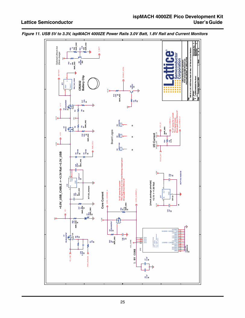
Table 4 describes the components on the board and the interfaces it supports.
Table 4. Pico Evaluation Board Components and Interfaces
Component/Interface Type Schematic Reference Description
Circuits
Power Circuit Circuit Figure 11 5V USB, 3V battery, and optional lithium-ion 20mA charge circuit.
High-Side Current Sense Circuit Circuit Figure 13
Resistive current sensor circuit to produce a voltage level proportional to the current level (see AN6049, High-side Current Sensing Techniques for Power Manager Devices).
USB Controller Circuit U4:FT2232D USB-to-JTAG interface and dual USB UART/FIFO IC.
USB Mini B Socket I/O J1:USB_MINI_B Programming and debug interface.
Components
LC4256ZE CPLD U1: Lattice_4kZE 256-macrocell CPLD packaged in a 7 x 7mm, 144-ball chip-scale BGA.
POWR6AT6 Mixed Signal PLD U6: ispPAC-POWR6AT6
Integrates analog DC-to-DC trim outputs, analog monitor, power supply margin/trim control, ADC, and I2C interface in a 32-ball QFNS package.
Interfaces
LCD Panel Output U2: LUMEX-LCD2 3-character, 7-segment LCD panel.
15x2 Header Landing I/O J2:HEADER 15X2 User-definable I/O.
4-Bit DIP Switch Input SW2: SWDIP-4 General purpose 4-bit DIP switch.
Push-button Switch Input SW1:GlobalReset General purpose push-button.
SubsystemsThis section describes the principle subsystems for the Pico board in alphabetical order.
BatteryA CR2032 watch cell battery provides a 3V supply rail for a portion of the Pico board and covers the LC4256ZE, current sensor circuit, and LCD power requirements. As a power saving measure a power MOSFET circuit enables the sensor circuit only upon measurement requests by the CPLD.
The Pico board can be populated by the user with a 20mA charger circuit for use with Li-Ion rechargable batteries only. Do not try to recharge a standard CR2032 battery.

17
ispMACH 4000ZE Pico Development KitLattice Semiconductor User’s Guide
Clock SourcesAll clocks for the Pico Power and GPIO I2C demonstration designs originate from the LC4256ZE CPLD on-chip oscillator and timer (OSCTIMER) block. You may use the expansion header landing to drive a CPLD input with an external clock source.
Current Sensor CircuitsThe board is populated with current sensor circuits connected to the VCC core and VCC I/O supply rails of the LC4256ZE CPLD. For more information see AN6049, High-side Current Sensing Techniques for Power Manager Devices.
DIP SwitchThe evaluation board includes a 4-bit input piano button style switch located on the bottom-right corner of the board. All four are available as general purpose inputs for the LC4256ZE.
Table 5. DIP Switch Reference
Item Description
Reference Designators SW2
Part Number 193-4MS
Manufacturer CTS
Web Site www.ctscorp.com
Table 6. DIP Switch Pin Information
SW2 Description LC4256ZE Pin
Expansion Header LandingThe expansion header provides user GPIOs connected to the LC4256ZE, VMON and TRIM analog I/Os connected to the POWR6AT6, and the on-board I2C/SMBus. The remaining pins serve as power supplies for external connec-tions. The expansion connector is con• gured as one 2x15 100mil centered pin header.
Table 7. Expansion Connector Reference
Item Description
Reference Designators J2
Part Number HEADER 15X2
Manufacturer Molex/Waldom Electronics
Web Site www.molex.com
Table 8. Expansion Header Pin Information
1 SW0 Input K11
2 SW1 Input J12
3 SW2 Input J11
4 SW3 Input H10
PinNumber Function
LC4256ZEPin
1 +3.1V N/A
2 VCCIO_EXT N/A
3 4K_TDI TDI
4 USB_TDI N/A
5 6AT6_TDO N/A
6 USB_TDO N/A

18
ispMACH 4000ZE Pico Development KitLattice Semiconductor User’s Guide
ispMACH4256ZE-MN144 CPLDThe ispMACH4256ZE-MN144 is a 144-ball csBGA package CPLD device which provides 108 I/Os and 4 dedicated inputs in a 7 x 7mm package.
Table 9. LC4256ZE CPLD Interface Reference
Item Description
Reference Designators U1
Part Number LC4256ZE
Manufacturer Lattice Semiconductor
Web Site www.latticesemi.com
JTAG Interface CircuitsFor power and programming an FTDI USB UART/FIFO IC converter provides a communication interface between a PC host and the JTAG programming chain of the Pico board. The USB 5V supply is also used as a source for the 3.3V and 1.8V supply rails. A USB B-type mini socket is provided for the USB connector cable.
Table 10. JTAG Interface Reference
Item Description
Reference Designators U4
Part Number FT2232D
Manufacturer FTDI (Future)
Web Site www.ftdichip.com
7 4K_TCK TCK
8 USB_TCK N/A
9 4K_TMS TMS
10 USB_TMS N/A
11 PROTO_K7 K7
12 USB_SDA N/A
13 PROTO_M7 M7
14 USB_SCL n/a
15 PROTO_K4 K4
16 PROTO_L7 L7
17 PROTO_M3 M3
18 PROTO_L8 L8
19 PROTO_L4 L4
20 PROTO_M8 M8
21 PROTO_M4 M4
22 PROTO_M9 M9
23 PROTO_K3 K3
24 PROTO_L9 L9
25 CLK0_MACH CLK0
26 PROTO_K8 K8
27 VMON_3 N/A
28 VMON_4 N/A
29 GND N/A
30 GND N/A

19
ispMACH 4000ZE Pico Development KitLattice Semiconductor User’s Guide
Table 11. JTAG Programming Pin Information
Description LC4256ZE Pin POWR6AT6 Pin/Net
Test Data Output B11:TDO / 4K_TDO 4:TDI / 6AT6_TDI
Test Data Output - 1:TDO / 6AT6_TDO
Test Data Input A1:TDI / 4K_TDI -
Test Mode Select M12:TMS / 4K_TMS 5:TMS / 6AT6_TMS
Test Clock L2:TCK / 4K_TCK 3:TCK / 6AT6_TCK
LCDA 3-character, 7-segment LCD panel is provided for CPLD outputs.
Table 12. LCD Reference
Item Description
Reference Designators U2
Part Number LCD-S301C31TR
Manufacturer Lumex
Web Site www.lumex.com
LEDA blue LED (POWR - D1) is used to indicate USB 5V power.
Table 13. User LEDs Reference
Item Description
Reference Designators D1
Part Number LTST-C190CKT
Manufacturer Lite-On
Web Site www.liteonit.com
Power Manager II ispPAC-POWR6AT6The ispPAC-POWR6AT6-01-SN32 Power Manager II device is a 32-ball QFNS package programmable mixed-sig-nal PLD which provides an interface between the on-board current sensor circuit and the I2C interface bus. The POWR6AT6 provides analog voltage monitors (VMON) and a 10-bit ADC to provide voltage measurements and an I2C interface to the LC4256ZE CPLD. The 15x2 External Header Landing provides access to VMON3 and VMON4 inputs for experiments with external circuit monitoring.
Table 14. ProcessorPM PLD Reference
Item Description
Reference Designators U6
Part Number ispPAC-POWR6AT6-01-SN32I
Manufacturer Lattice Semiconductor
Web Site www.latticesemi.com
Power SupplyTwo optional power sources are provided depending on jumper settings. A 3.0V supply rail is provided from the bat-tery and can power a subset of the board including the ispMACH 4000ZE, current sensor circuit, and LCD panel. Alternatively 3.3V and 1.8V supply rails are converted from the USB 5V interface when the board is connected to a host PC. The ispMACH4000ZE device will be isolated from other subsystems to accommodate accurate cur-rent/power measurements.

20
ispMACH 4000ZE Pico Development KitLattice Semiconductor User’s Guide
Pushbutton SwitchThe board has one momentary push-button switch (S1). You may use the switch as a user-defined input for your own custom CPLD designs.
Table 15. Push-button Reference
Item Description
Reference Designators S1
Part Number EVQ-Q2K03W
Manufacturer Panasonic ECG
Web Site www.panasonic.com/industrial/components/components.html
Table 16. Push-button Pin Information
Button Description (Pre-Programmed Pico Power) ProcessorPM Pin
Test PointsIn order to check the various voltage levels used, test points are provided:
• R35, VCC (CORE)
• R34, VCCIO of all banks
USB Programming and Debug InterfaceThe USB B-type Mini socket of the Pico board serves as the programming and debug interface.
JTAG Programming: For JTAG programming a preprogrammed USB PHY peripheral controller is provided on the Pico board to serve as the programming interface to the ispMACH 4000ZE CPLD.
Programming requires the ispVM System software (www.latticesemi.com/ispvm). The programming connection will appear to the ispVM System software as if a regular parallel-type ispDOWNLOAD™ cable is connected to the PC.
Modifying the Pico BoardThe ispMACH 4000ZE Pico evaluation board provides landing areas for additional circuits to support the following functions:
• Rechargeable Lithium-Ion 20 mA rechargeable battery
• 15x2 Header
Note: Modifying your board requires good electronics handling and PCB fabrication techniques to avoid damage.
Add Support for a Rechargeable BatteryThe Pico board can be upgraded to support a Lithium-Ion rechargeable battery. When connected to a PC’s USB port the battery circuit will recharge the battery cell. Install R23, R26, R42 and Q6 (Figure 11) to provide a 20mA constant current charge.
15x2 HeaderInstall a 30-pin header at location J2 – HEADER 15x2 (Figure 10).
Mechanical SpecificationsDimensions: 2 ½ in. [L] x 2 in. [W] x 3/8 in. [H]
S1 Pico board reset H11

21
ispMACH 4000ZE Pico Development KitLattice Semiconductor User’s Guide
Environmental RequirementsThe evaluation board must be stored between -40°C and 100°C. The recommended operating temperature is between 0°C and 90°C.
The evaluation board can be damaged without proper anti-static handling.
GlossaryCPLD: Complex Programmable Logic Device
DIP: Dual in-line package.
I2C: Inter-Integrated Circuit.
LED: Light Emitting Diode.
Mixed Signal PLD: A PLD integrated with analog and mixed signal support circuitry.
PCB: Printed Circuit Board.
RoHS: Restriction of Hazardous Substances Directive.
PLL: Phase Locked Loop.
SPI: Serial Peripheral Interface.
SRAM: Static Random Access Memory.
TransFR: Transparent Field Reconfiguration.
UART: Universal Asynchronous Receiver/Transmitter.
USB: Universal Serial Bus.
WDT: Watchdog timer
TroubleshootingNo Current/Voltage Meter Readings AvailableA low battery can cause the current/voltage meter features of the Pico Power demo to read 0µA/0V. The demo’s counter and shift register features may operate but the additional current required to energize the current sensor and POWR6AT6 may not be available once the battery begins to discharge. Install a new battery if this condition occurs.
Determine the Source of a Pre-Programmed PartIt is possible that you may receive your Pico board after it has been reprogrammed by someone else. To restore the board to the factory default, see the Download Demo Designs for details on downloading and reprogramming the device.
You can also determine which demo design is currently programmed onto the Pico board by comparing the JEDEC checksums against of the programming file with what is read from the programmed part.
To compare JEDEC file checksum:
1. Connect the Pico board to a host PC using the USB port.
2. Start ispVM and choose ispTools > Scan. The POWR605 and POWR6AT6 devices appear in the Device List.
3. Double-click the device row. The Device Information dialog appears.

22
ispMACH 4000ZE Pico Development KitLattice Semiconductor User’s Guide
4. Click the Browse button. The Save as Data File dialog appears.
5. Specify a new JEDEC Data File name and click the Save button.
6. From the Operation list choose Read and Save JEDEC and click OK.
7. Choose Project > Download. ispVM reads the contents from the device and writes the results to the JEDEC file specified.
Open the JEDEC file into a text editor and page to the bottom of the file.
Note the hexidecimal checksum at the line above the User Electronic Data note line. Compare this value against the checksum of the original JEDEC demo programming files.
Ordering Information
Description Ordering Part NumberChina RoHS Environment-Friendly
Use Period (EFUP)
IspMACH 4000ZE Pico Development Kit LC4256ZE-P-EVN
Technical Support AssistanceHotline: 1-800-LATTICE (North America)
+1-503-268-8001 (Outside North America)e-mail: [email protected]: www.latticesemi.com
Revision HistoryDate Version Change Summary
September 2009 01.0 Initial release.
© 2009 Lattice Semiconductor Corp. All Lattice trademarks, registered trademarks, patents, and disclaimers are as listed at www.latticesemi.com/legal. All other brand or product names are trademarks or registered trademarks of their respective holders. The speci• cations and information herein are subject to change without notice.

23
ispMACH 4000ZE Pico Development KitLattice Semiconductor User’s Guide
Appendix A. SchematicsFigure 9. ispMACH 4000ZE Bank 0 and 3-Digit LCD
5 5
4 4
3 3
2 2
1 1
DD
CC
BB
AA
LCD
_C1
LCD
_DP
2
LCD
_E2
LCD
_D2
LCD
_DP
1
LCD
_E1
LCD
_D1
LCD
_B1
LCD
_F2
LCD
_A2
LCD
_B2
LCD
_G1
LCD
_F1
LCD
_A1
LCD
_G2
LCD
_C2
LCD
_G1
LCD
_F1
LCD
_A1
LCD
_B1
LCD
_G2
LCD
_F2
LCD
_A2
LCD
_B2
LCD
_G3
LCD
_F3
LCD
_A3
LCD
_B3
LCD
_E1
LCD
_D1
LCD
_C1
LCD
_DP
1
LCD
_E2
LCD
_D2
LCD
_C2
LCD
_DP
2
LCD
_E3
LCD
_D3
LCD
_C3
LCD
_A3
LCD
_B3
LCD
_C3
LCD
_D3
LCD
_E3
LCD
_F3
LCD
_G3
CO
M_L
CD
CO
M_L
CD
4K_S
CL
4K_S
DA
+3.1
V
VC
C_I
O
VC
C_I
O
4K_T
DI
4K_T
CK
PR
OTO
_K4
PR
OTO
_M3
PR
OTO
_L4
PR
OTO
_M4
CLK
0_M
AC
H
PR
OTO
_K3
BD
BU
S2
BD
BU
S3
BD
BU
S4
BD
BU
S5
BD
BU
S6
BD
BU
S7
BD
BU
S1
BD
BU
S0
VC
C_I
O
+3.1
V
6AT6
_SC
L6A
T6_S
DA
US
B_S
CL
US
B_S
DA
EN
AB
LE_6
AT6
b+3
.3V
Dat
e:
Siz
eS
chem
atic
Rev
ofS
heet
Title
Latti
ce S
emic
ondu
ctor
App
licat
ions
Em
ail:
tech
supp
ort@
Latti
cese
mi.c
omP
hone
(503
) 268
-800
1 -o
r- (8
00) L
ATT
ICE
Boa
rd R
ev
Pro
ject
Thur
sday
, Aug
ust 6
, 200
9
B
51
4KZE
Ban
k 0
and
3-D
igit
LCD
ispM
AC
H40
00ZE
Pic
o B
oard
CC
Dat
e:
Siz
eS
chem
atic
Rev
ofS
heet
Title
Latti
ce S
emic
ondu
ctor
App
licat
ions
Em
ail:
tech
supp
ort@
Latti
cese
mi.c
omP
hone
(503
) 268
-800
1 -o
r- (8
00) L
ATT
ICE
Boa
rd R
ev
Pro
ject
Thur
sday
, Aug
ust 6
, 200
9
B
51
4KZE
Ban
k 0
and
3-D
igit
LCD
ispM
AC
H40
00ZE
Pic
o B
oard
CC
Dat
e:
Siz
eS
chem
atic
Rev
ofS
heet
Title
Latti
ce S
emic
ondu
ctor
App
licat
ions
Em
ail:
tech
supp
ort@
Latti
cese
mi.c
omP
hone
(503
) 268
-800
1 -o
r- (8
00) L
ATT
ICE
Boa
rd R
ev
Pro
ject
Thur
sday
, Aug
ust 6
, 200
9
B
51
4KZE
Ban
k 0
and
3-D
igit
LCD
ispM
AC
H40
00ZE
Pic
o B
oard
CC
Bank 0
To FT chip
To P
roto
Pin
Lattice Semiconductor : LC4256ZE-05MN144C
Need
to
draw
foo
t pr
int
.10
0" a
part
hol
es D
IPsi
ze,
24
hole
s .7
13"
wide
. To
tal
Glas
s si
ze1.
21"
long
plu
s bu
mp
n/c
n/c
n/c
n/c
Part
#
LCD-
S301
C31T
R
U12
STG
3690
QTR D
IQ
FN16
U12
STG
3690
QTR D
IQ
FN16
1S2
1
1-2I
N2
2S1
3D
24
2S2
5
GN
D6
3S1
7
D3
8
3S2
93-
4IN
104S
111
D4
12
4S2
13
VC
C14
1S1
15
D1
16
R45
10k
DI
R45
10k
DI
R46 10
k DI
R46 10
k DI
C2
0.1u
FD
I
C2
0.1u
FD
I
C1
0.1u
FD
I
C1
0.1u
FD
I
ispM
ACH4
000Z
E14
4 cs
BGA
Pin
name
seq
uenc
e(6
4,12
8,25
6)
Latti
ce_4
kZE
U1A
PC
B F
ootp
rint =
CS
BG
A14
4D
IispM
ACH4
000Z
E14
4 cs
BGA
Pin
name
seq
uenc
e(6
4,12
8,25
6)
Latti
ce_4
kZE
U1A
PC
B F
ootp
rint =
CS
BG
A14
4D
I
TDI
A1
NC
/ IO
B0
/ IO
C6
B2
NC
/ IO
B1
/ IO
C5
B1
IOA
8 / I
OB
2 / I
OC
4C
3IO
A9
/ IO
B3
/ IO
C3
C2
IOA
10 /
IOB
4 / I
OC
2C
1IO
A11
/ IO
B5
/ IO
C1
D1
NC
/ N
C /
IOD
7D
2N
C /
NC
/ IO
D6
D3
NC
/ IO
B6
/ IO
D5
E1
IOA
12 /
IOB
7 / I
OD
4E
2IO
A13
/ IO
B8
/ IO
D3
F2IO
A14
/ IO
B9
/ IO
D2
D4
IOA
15 /
IOB
10 /
IOD
1F1
DI0
/ IO
B11
/ IO
D0
F3IO
B15
/ IO
C11
/ IO
E0
G1
IOB
14 /
IOC
10 /
IOE
1E
3IO
B13
/ IO
C9
/ IO
E2
G2
IOB
12 /
IOC
8 / I
OE
3G
3N
C /
IOC
7 / I
OE
4H
1N
C /
IOC
6 / I
OE
5H
3N
C /
NC
/ IO
E6
H2
IOB
11 /
IOC
5 / I
OF1
J1IO
B10
/ IO
C4
/ IO
F2J3
IOB
9 / I
OC
3 / I
OF3
J2IO
B8
/ IO
C2
/ IO
F4K
1D
I1 /
IOC
1 / I
OF5
K2
NC
/ IO
C0
/ IO
F6L1
TCK
L2N
C /
NC
/ IO
G7
M1
NC
/ N
C /
IOG
6K
3N
C /
IOD
11 /
IOG
5M
2D
I2 /
IOD
10 /
IOG
4L3
IOB
7 / I
OD
9 / I
OG
3J4
IOB
6 / I
OD
8 / I
OG
2K
4IO
B5
/ IO
D7
/ IO
G1
M3
IOB
4 / I
OD
6 / I
OG
0L4
NC
/ IO
D5
/ IO
H6
M4
NC
/ IO
D4
/ IO
H5
L5IO
B3
/ IO
D3
/ IO
H4
K5
IOB
2 / I
OD
2 / I
OH
3J6
IOB
1 / I
OD
1 / I
OH
2M
5IO
B0
/ IO
D0
/ IO
H1
K6
CLK
1*I
L6C
LK0*
IA
7IO
A0*
OE
0 / I
OA
0*O
E0
/ IO
A1*
OE
0D
6IO
A1
/ IO
A1
/ IO
A2
B6
IOA
2 / I
OA
2 / I
OA
3A
6IO
A3
/ IO
A3
/ IO
A4
C6
NC
/ IO
A4
/ IO
A5
B5
NC
/ IO
A5
/ IO
A6
A5
IOA
4 / I
OA
6 / I
OB
1A
4IO
A5
/ IO
A7
/ IO
B2
B4
IOA
6 / I
OA
8 / I
OB
3C
5IO
A7
/ IO
A9
/ IO
B4
A3
NC
/ IO
A10
/ IO
B5
C4
NC
/ IO
A11
/ IO
B6
B3
NC
/ N
C /
IOB
7A
2
NC / VCCIO0 / VCCIO0E4VCCIO0F4
NC / VCCIO0 / VCCIO0G4VCCIO0J5VCCIO0D5
U2
LUM
EX
-LC
D2
PC
B F
ootp
rint =
LU
ME
X30
1
DIU
2
LUM
EX
-LC
D2
PC
B F
ootp
rint =
LU
ME
X30
1
DI
F219
A2
18
G2
20
B2
17
G3
16
B3
13
F315
A3
14
D2
7
E2
6
DP
15
CO
M1
C2
8
DP
29
B1
21
E1
2
E3
10
D3
11
D1
3
C1
4
C3
12
G1
24
A1
22
F123
C35
0.1u
FD
I
C35
0.1u
FD
I

24
ispMACH 4000ZE Pico Development KitLattice Semiconductor User’s Guide
Figure 10. ispMACH 4000ZE Bank 1, DIP, SW, Expansion Header
5 5
4 4
3 3
2 2
1 1
DD
CC
BB
AA
SW
1S
W0
SW
2S
W3
PR
OTO
_K7
PR
OTO
_M7
PR
OTO
_L7
PR
OTO
_M9
PR
OTO
_L9
PR
OTO
_K8
PR
OTO
_M8
PR
OTO
_L8
SW
0S
W1
SW
2S
W3
VC
C_I
O
VC
CIO
_EX
TV
CC
IO_E
XT
4K_T
MS
PR
OTO
_K4
PR
OTO
_M3
PR
OTO
_L4
PR
OTO
_M4
EN
AB
LE_6
AT6
b
4K_T
DO
PR
OTO
_K3
4K_T
MS
4K_T
DI
US
B_T
DI
US
B_T
CK
US
B_T
MS
6AT6
_TD
OU
SB
_TD
O
CLK
0_M
AC
HV
MO
N_4
VM
ON
_3
US
B_S
DA
US
B_S
CL
PR
OTO
_K7
PR
OTO
_M7
+3.1
V
VC
CIO
_EX
T
VC
C_I
O
4K_T
CK
Dat
e:
Siz
eS
chem
atic
Rev
ofS
heet
Title
Latti
ce S
emic
ondu
ctor
App
licat
ions
Em
ail:
tech
supp
ort@
Latti
cese
mi.c
omP
hone
(503
) 268
-800
1 -o
r- (8
00) L
ATT
ICE
Boa
rd R
ev
Pro
ject
Thur
sday
, Aug
ust 6
, 200
9
B
52
4KZE
Ban
k 1,
DIP
SW
, Exp
ansi
on H
eade
r
ispM
AC
H40
00ZE
Pic
o B
oard
CC
Bank 1
Not
e: A
dd ju
mpe
rs in
cop
per(
on b
otto
m -
laye
r # 4
).A
t pin
s 1,
3, 5
, 7, 9
of J
2C
ut to
mod
ify th
e JT
AG
cha
in.
Part
Num
ber:
EVQ
Q2K0
3WPa
naso
nic
SMD
CT19
34MS
-ND
n/c
n/c
n/c
n/c
C3
0.1u
F DI
SM
/C_0
402
C3
0.1u
F DI
SM
/C_0
402
C5
0.1u
FD
I
C5
0.1u
FD
I
C4
0.1u
FD
I
C4
0.1u
FD
I
R13
100k
DI
R13
100k
DI
ispM
ACH4
000Z
E14
4 cs
BGA
Pin
name
seq
uenc
e(6
4,12
8,25
6)
Latti
ce_4
kZE
U1B
CS
BG
A14
4
DIis
pMAC
H400
0ZE
144
csBG
APi
n na
me s
eque
nce
(64,
128,
256)
Latti
ce_4
kZE
U1B
CS
BG
A14
4
DI
CLK
2*I
M6
IOC
0 / I
OE
0 / I
OI1
K7
IOC
1 / I
OE
1 / I
OI2
M7
IOC
2 / I
OE
2 / I
OI3
L7IO
C3
/ IO
E3
/ IO
I4J7
NC
/ IO
E4
/ IO
I5L8
NC
/ IO
E5
/ IO
I6M
8IO
C4
/ IO
E6
/ IO
J1M
9IO
C5
/ IO
E7
/ IO
J2L9
IOC
6 / I
OE
8 / I
OJ3
K8
IOC
7 / I
OE
9 / I
OJ4
M10
NC
/ IO
E10
/ IO
J5L1
0N
C /
IOE
11 /
IOJ6
K9
NC
/ N
C /
IOJ7
M11
TMS
M12
NC
/ IO
F0 /
IOK
6L1
2N
C /
IOF1
/ IO
K5
L11
IOC
8 / I
OF2
/ IO
K4
K10
IOC
9 / I
OF3
/ IO
K3
K12
IOC
10 /
IOF4
/ IO
K2
J10
IOC
11 /
IOF5
/ IO
K1
K11
NC
/ N
C /
IOL7
J12
NC
/ N
C /
IOL6
J11
NC
/ IO
F6 /
IOL5
H10
IOC
12 /
IOF7
/ IO
L4H
12IO
C13
/ IO
F8 /
IOL3
G11
IOC
14 /
IOF9
/ IO
L2H
11IO
C15
/ IO
F10
/ IO
L1G
12D
I3 /
IOF1
1 / I
OL0
G10
IOD
15 /
IOG
11 /
IOM
0F1
2IO
D14
/ IO
G10
/ IO
M1
F11
IOD
13 /
IOG
9 / I
OM
2E
11IO
D12
/ IO
G8
/ IO
M3
E12
NC
/ IO
G7
/ IO
M4
D10
NC
/ IO
G6
/ IO
M5
F10
NC
/ N
C /
IOM
6D
12IO
D11
/ IO
G5
/ IO
N1
E10
IOD
10 /
IOG
4 / I
ON
2D
11IO
D9
/ IO
G3
/ IO
N3
E9
IOD
8 / I
OG
2 / I
ON
4C
12D
I4 /
IOG
1 / I
ON
5C
11N
C /
IOG
0 / I
ON
6B
12TD
OB
11N
C /
NC
/ IO
O7
A12
NC
/ N
C /
IOO
6C
10N
C /
IOH
11 /
IOO
5B
10D
I5 /
IOH
10 /
IOO
4A
11IO
D7
/ IO
H9
/ IO
O3
D9
IOD
6 / I
OH
8 / I
OO
2B
9IO
D5
/ IO
H7
/ IO
O1
C9
IOD
4 / I
OH
6 / I
OO
0A
10N
C /
IOH
5 / I
OP
6A
9N
C /
IOH
4 / I
OP
5B
8IO
D3
/ IO
H3
/ IO
P4
C8
IOD
2 / I
OH
2 / I
OP
3A
8IO
D1
/ IO
H1
/ IO
P2
D7
IOD
0*O
E1
/ IO
H0*
OE
1 / I
OP
1*O
E1
B7
CLK
3*I
C7
VCCIO1J8NC / VCCIO1 / VCCIO1H9
VCCIO1G9NC / VCCIO1 / VCCIO1F9
VCCIO1D8
S1
Glo
balR
eset
PC
B F
ootp
rint =
SM
T_S
W
DI
S1
Glo
balR
eset
PC
B F
ootp
rint =
SM
T_S
W
DI
14
23
J2 HE
AD
ER
15X
2
J2 HE
AD
ER
15X
2
2 4 6 8 10 12 14 16 18 20 22 24 26 28 30
1 3 5 7 9 11 13 15 17 19 21 23 25 27 29
R12
100k
DI
R12
100k
DI
R15
100k
DI
R15
100k
DI
D4
1N41
48D
I
D4
1N41
48D
I
R11
100k
DI
R11
100k
DI
R14
100k
DI
R14
100k
DI
SW
2
SW
DIP
-4
DI
SW
2
SW
DIP
-4
DI
1 2 3 4
8 7 6 5
25
ispMACH 4000ZE Pico Development KitLattice Semiconductor User’s Guide
Figure 11. USB 5V to 3.3V, ispMACH 4000ZE Power Rails 3.0V Batt, 1.8V Rail and Current Monitors
5 5
4 4
3 3
2 2
1 1
DD
CC
BB
AA
+3.1
V
VC
C_I
OV
CC
IO_E
XT
+3.1
V+1
.8V
+1.8
V
VC
C_C
OR
E
+5V
+3.3
V+5
V
+3.1
V
+5V
+5V
CO
RE
_CU
RR
EN
T_H
CO
RE
_CU
RR
EN
T_L
V_B
ATT
IO_C
UR
RE
NT_
L
IO_C
UR
RE
NT_
H
+5V
_US
B
PW
R_V
CC
J
PW
R_E
NA
BLE
b
+5V
VC
C_I
OV
CC
IO_E
XT
+3.1
VB
ATT
ER
Y
EN
AB
LE_6
AT6
b
+3.3
V
Dat
e:
Siz
eS
chem
atic
Rev
ofS
heet
Title
Latti
ce S
emic
ondu
ctor
App
licat
ions
Em
ail:
tech
supp
ort@
Latti
cese
mi.c
omP
hone
(503
) 268
-800
1 -o
r- (8
00) L
ATT
ICE
Boa
rd R
ev
Pro
ject
Thur
sday
, Aug
ust 6
, 200
9
B
53
US
B 5
V to
3.3
V, 4
KZE
Pow
er R
ails
3.0
V B
att,
1.8V
Rai
l and
Cur
rent
Mon
itors
ispM
AC
H40
00ZE
Pic
o B
oard
CC
Opt
iona
l Lith
ium
-Ion
20m
A c
harg
er
Cor
e C
urre
nt
I/O C
urre
nt+3
.1V
-> +
1.8V
Rai
l[c
heck
pac
kage
pin
s/ta
b]
CR
2032
Bat
tery
Clip
1.8V
COR
E
To U
7 se
nse
for c
urre
ntTh
in s
igna
l tra
ces
Dire
ct p
ath
from
R34
to U
7
+5.0
V_U
SB_C
AB
LE ->
+3.
3V R
ail +
3.3V
_USB
To U
7 se
nse
for c
urre
ntTh
in s
igna
l tra
ces
or n
on lo
ad b
earin
g co
pper
pou
rD
irect
pat
h fr
om R
35 to
U7
Boar
d Lo
gos
R34
100
SM
/R_0
603
DI
0.1%
R34
100
SM
/R_0
603
DI
0.1%
R3
10k
DI
R3
10k
DI
R43
1M DI
SM
/R_0
603
R43
1M DI
SM
/R_0
603
D1
Blu
e
DI
SM
/D_0
603
D1
Blu
e
DI
SM
/D_0
603
G4
Latti
ce L
ogo
DI
G4
Latti
ce L
ogo
DI1
D2
1N41
48D
I
D2
1N41
48D
I
U11
MC
P17
03-1
802E
/CB
SO
T-23
DI
U11
MC
P17
03-1
802E
/CB
SO
T-23
DI
GN
D
1
IN3
OU
T2
BT1
Bat
t_C
ell_
Hol
der
BT1
Bat
t_C
ell_
Hol
der
Vba
t+3
Vba
t+2
2
V-
1
C30
10uF
DI
SM
/C_0
402
C30
10uF
DI
SM
/C_0
402
G5
E-F
riend
ly
DI
G5
E-F
riend
ly
DI1
R17
100k
DI
R17
100k
DI
C32
1uF
DI
C32
1uF
DI
C31
1uF
DI
C31
1uF
DI
ispM
ACH4
000Z
E14
4 cs
BGA
Pin
name
seq
uenc
e(6
4,12
8,25
6)
Latti
ce_4
kZE
U1C
CS
BG
A14
4D
I
ispM
ACH4
000Z
E14
4 cs
BGA
Pin
name
seq
uenc
e(6
4,12
8,25
6)
Latti
ce_4
kZE
U1C
CS
BG
A14
4D
I
VCCH5VCCH8VCCE8VCCE5
GND F6GNDIO0 G5GNDIO0 H4GND G6GNDIO0 H6NC / GNDIO1 / GNDIO1 H7GNDIO1 J9GND G7GNDIO1 G8GNDIO1 F8GND F7GNDIO1 E7NC / GNDIO0 / GNDIO0 E6GNDIO0 F5
R4
10k
DI
R4
10k
DI
Q3
IRLM
L640
2PbF
DI
Q3
IRLM
L640
2PbF
DI
Q5
2N22
22D
I
Q5
2N22
22D
I
Q6
2N39
06D
NI
Q6
2N39
06D
NI
C6
0.1u
FD
I
C6
0.1u
FD
I
R42
15 DN
IS
M/R
_040
2
R42
15 DN
IS
M/R
_040
2
Q1
IRLM
L640
2PbF DI
Q1
IRLM
L640
2PbF DI
C29
6.8u
FD
IS
M/C
_040
2
C29
6.8u
FD
IS
M/C
_040
2
R35
50 SM
/R_0
603
DI
0.1%
R35
50 SM
/R_0
603
DI
0.1%
R2
10k
DI
SM
/R_0
402
R2
10k
DI
SM
/R_0
402
R27 1k DI
SM
/R_0
402
R27 1k DI
SM
/R_0
402
D3
1N41
48D
I
D3
1N41
48D
I
R23 4.
2kD
NI
SM
/R_0
402
R23 4.
2kD
NI
SM
/R_0
402
C7
0.1u
FD
I
C7
0.1u
FD
I
R20
4.7k
DI
SM
/R_0
402
R20
4.7k
DI
SM
/R_0
402
Q2
IRLM
L640
2PbF
DI
Q2
IRLM
L640
2PbF
DI
R1
10k
DI
R1
10k
DI
Q4
IRF2
40Q4
IRF2
40
G6
WE
EE
DI
G6
WE
EE
DI1
R16
100k D
IS
M/R
_040
2
R16
100k D
IS
M/R
_040
2
R18
100k D
IS
M/R
_040
2
R18
100k D
IS
M/R
_040
2
U10
NC
P11
17D
I
SO
T-22
3_ch
eckp
insU
10
NC
P11
17D
I
SO
T-22
3_ch
eckp
ins
GN
D
1
IN3
OU
T2
TAB
4
C36 1uF DI
C36 1uF DI
C28
0.33
uFD
I
C28
0.33
uFD
I
R26 1k
DN
IS
M/R
_040
2
R26 1k
DN
IS
M/R
_040
2R
91M D
I
R9
1M DI

26
ispMACH 4000ZE Pico Development KitLattice Semiconductor User’s Guide
Figure 12. USB to JTAG and I2C for the ispMACH 4000ZE and ispPAC-POWR6AT6
5 5
4 4
3 3
2 2
1 1
DD
CC
BB
AA
EE
CS
EE
SK
EE
DA
TA
SH
LD_D
ebug
+5V
_US
B
+3.3
V+5
V_U
SB
+5V
_US
B
+3.1
V
BD
BU
S2
BD
BU
S3
BD
BU
S4
BD
BU
S5
BD
BU
S6
BD
BU
S7
PW
R_E
NA
BLE
b
US
B_S
CL
US
B_T
CK
US
B_T
DI
US
B_T
DO
US
B_T
MS
US
B_S
DA
BD
BU
S1
BD
BU
S0
+5V
_US
B
+3.1
V
+3.3
V
Dat
e:
Siz
eS
chem
atic
Rev
ofS
heet
Title
Latti
ce S
emic
ondu
ctor
App
licat
ions
Em
ail:
tech
supp
ort@
Latti
cese
mi.c
omP
hone
(503
) 268
-800
1 -o
r- (8
00) L
ATT
ICE
Boa
rd R
ev
Pro
ject
Thur
sday
, Aug
ust 6
, 200
9
B
54
US
B to
JTA
G a
nd I2
C fo
r the
4K
ZE a
nd 6
AT6
ispM
AC
H40
00ZE
Pic
o B
oard
CC
18pF
= 12
pF +
Gro
und P
lane (
6pF
)
USB
Con
nect
ion
JTAG TO MACH-4KZE
and POWR6AT6
M93C
46-W
MN6T
P Ma
nuf:
ST M
icro
Digi
-Key
Par
t Nu
mber
497
-509
0-1-
ND
Hig
h =
JTA
GLo
w =
I2C
RN
1F0
RN
1F0
611
R28
1kD
I
R28
1kD
I
J1U
SB
_MIN
I_B
DI
TYP
E_B
J1U
SB
_MIN
I_B
DI
TYP
E_B
VC
C1
D-
2D
+3
GN
D5
NC
4
CA
SE
7C
AS
E8
CA
SE
9
CA
SE
6
MH
110
MH
211
C19
12pF
DI
C19
12pF
DI
RN
1E0
RN
1E0
512
R6
10k
DI
R6
10k
DI
C9
0.1u
FD
I
C9
0.1u
FD
I
RN
1D0
RN
1D0
413
C10
0.1u
FD
I
C10
0.1u
FD
I
C12
0.1u
F DI
C12
0.1u
F DI
C11
0.1u
FD
I
C11
0.1u
FD
I
U3
M93
C46
-W
SO
IC-8
DI
U3
M93
C46
-W
SO
IC-8
DI
CS
1S
K2
DIN
3D
OU
T4
VC
C8
NC
7O
RG
6G
ND
5
R33
330
DI
R33
330
DI
C21
33pF
DI
C21
33pF
DI
U5 S
TG36
90Q
TR
DI
QFN
16
U5 S
TG36
90Q
TR
DI
QFN
161S2
1
1-2I
N2
2S1
3D
24
2S2
5
GN
D6
3S1
7
D3
8
3S2
93-
4IN
104S
111
D4
12
4S2
13
VC
C14
1S1
15
D1
16
RN
1C0
RN
1C0
314
R5
10k
SM
/R_0
402
R5
10k
SM
/R_0
402
L1 Ferr
ite_b
ead
SM
/R_0
603
DI
L1 Ferr
ite_b
ead
SM
/R_0
603
DI
U4
FT22
32D
TQFP
-48
DI
U4
FT22
32D
TQFP
-48
DI
RS
TOU
T#5
XTO
UT
44
RE
SE
T#4
EE
CS
48
EE
SK
1
EE
DA
TA2
AGND 45
GND 9GND 18
TES
T47
3V3O
UT
6
AVCC46
VCC42 VCC3
US
BD
M8
US
BD
P7
XTI
N43
TXD
A24
RX
DA
23R
TSA
#22
CTS
A#
21D
TRA
#20
DS
RA
#19
DC
DA
#17
RIA
#16
TXD
EN
A15
SLE
EP
A#
13R
XLE
D#
12TX
LED
#11
SI/W
UA
10
TXD
B40
RX
DB
39R
TSB
#38
CTS
B#
37D
TRB
#36
DR
SB
#35
DC
DB
#33
RIB
#32
TXD
EN
B#
30S
LEE
PB
#29
RX
LED
B#
28TX
LED
B#
27
SI/W
UB
26
PW
RE
N#
41
GND 25GND 34VCCIOA14
VCCIOB31
C27
33nF D
I
C27
33nF D
I
R24
2.2k
R24
2.2k
C8
0.1u
FC
80.
1uF
C22
33pF
DI
C22
33pF
DI
RN
1B0
RN
1B0
215
R44
1M DI
R44
1M DI
R19
100k
DI
R19
100k
DI
C23
10nF
DI
SM
/C_0
402
C23
10nF
DI
SM
/C_0
402
C33
0.1u
FD
I
C33
0.1u
FD
I
R40
27
DI
SM
/R_0
402
R40
27
DI
SM
/R_0
402
RN
1H0
RN
1H0
89
R25 1.
5kD
IR25 1.
5kD
I
X1
6MH
z
XTA
L_H
CM
49
DI
X1
6MH
z
XTA
L_H
CM
49
DI
12
C34
0.1u
FD
I
C34
0.1u
FD
I
C2410nF
DI
C2410nF
DI
RN
1A0
DN
I
RN
1A0
DN
I
116
RN
1G0
RN
1G0
710
C20
12pF
DI
C20
12pF
DI
R41
27
DI
SM
/R_0
402
R41
27
DI
SM
/R_0
402
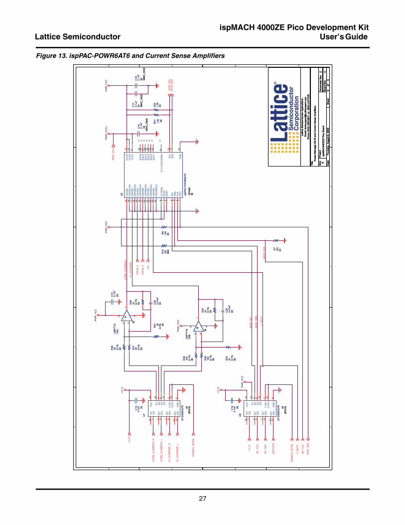
27
ispMACH 4000ZE Pico Development KitLattice Semiconductor User’s Guide
Figure 13. ispPAC-POWR6AT6 and Current Sense Amplifiers
5 5
4 4
3 3
2 2
1 1
DD
CC
BB
AA
CO
RE
_CU
RR
EN
T
IO_C
UR
RE
NT
V_B
ATT
6AT6
_TC
K
6AT6
_TD
I
6AT6
_TM
S
PW
R_V
CC
PW
R_V
CC
PW
R_V
CC
PW
R_V
CC
JP
WR
_VC
C
+3.1
V
+3.1
V PW
R_V
CC
6AT6
_TD
O
4K_T
CK
4K_T
MS
4K_T
DO
6AT6
_SD
A6A
T6_S
CL
VM
ON
_3
VM
ON
_4
+5V
PW
R_V
CC
J
CO
RE
_CU
RR
EN
T_H
CO
RE
_CU
RR
EN
T_L
IO_C
UR
RE
NT_
H
IO_C
UR
RE
NT_
L
EN
AB
LE_6
AT6
b
+3.1
V
BA
TTE
RY
EN
AB
LE_6
AT6
b
V_B
ATT
+3.1
V
Dat
e:
Siz
eS
chem
atic
Rev
ofS
heet
Title
Latti
ce S
emic
ondu
ctor
App
licat
ions
Em
ail:
tech
supp
ort@
Latti
cese
mi.c
omP
hone
(503
) 268
-800
1 -o
r- (8
00) L
ATT
ICE
Boa
rd R
ev
Pro
ject
Thur
sday
, Aug
ust 6
, 200
9
BC
55
Pow
er M
anag
er 6
AT6
and
Cur
rent
Sen
se A
mpl
ifier
s
ispM
AC
H40
00ZE
Pic
o B
oard
CD
ate:
Siz
eS
chem
atic
Rev
ofS
heet
Title
Latti
ce S
emic
ondu
ctor
App
licat
ions
Em
ail:
tech
supp
ort@
Latti
cese
mi.c
omP
hone
(503
) 268
-800
1 -o
r- (8
00) L
ATT
ICE
Boa
rd R
ev
Pro
ject
Thur
sday
, Aug
ust 6
, 200
9
BC
55
Pow
er M
anag
er 6
AT6
and
Cur
rent
Sen
se A
mpl
ifier
s
ispM
AC
H40
00ZE
Pic
o B
oard
C
NC NCNC NC NC NCNC
R8
10k
DIR8
10k
DI
R22
1.5k
DI
R22
1.5k
DI
R31 2k D
I0.
1%R31 2k D
I0.
1%
C16
0.1u
FD
IS
M/C
_040
2
C16
0.1u
FD
IS
M/C
_040
2U
7
STG
3690
QTR D
IQ
FN16
U7
STG
3690
QTR D
IQ
FN16
1S2
1
1-2I
N2
2S1
3D
24
2S2
5
GN
D6
3S1
7
D3
8
3S2
93-
4IN
104S
111
D4
12
4S2
13
VC
C14
1S1
15
D1
16
R10
10k
DN
I
R10
10k
DN
I
-+
U9B
LMP
7716 D
IB-+
U9B
LMP
7716 D
IB5 6
78 4
C17
0.1u
FD
IS
M/C
_040
2
C17
0.1u
FD
IS
M/C
_040
2
R36
50 DI
0.1%
R36
50 DI
0.1%
C25
0.01
uFD
I
C25
0.01
uFD
I
R37
50 DI
0.1%
R37
50 DI
0.1%
C14
0.1u
F DI
C14
0.1u
F DI
R29
2k DI
0.1%
R29
2k DI
0.1%
R38
100
DI
0.1%
R38
100
DI
0.1%
R39
100
DI
0.1%
R39
100
DI
0.1%
R7
10k
DIR7
10k
DI
C26
0.01
uFD
I
C26
0.01
uFD
I
U6 ispP
AC
-PO
WR
6AT6
QFN
32D
I
U6 ispP
AC
-PO
WR
6AT6
QFN
32D
I
VM
ON
115
VM
ON
217
VM
ON
319
VM
ON
421
VM
ON
523
VM
ON
625
VM
ON
1GS
14
VM
ON
2GS
16
VM
ON
3GS
18
VM
ON
4GS
20
VM
ON
5GS
22
VM
ON
6GS
24
TDI
4TM
S5
TCK
3TD
O1
DA
C6
26D
AC
527
DA
C4
28D
AC
329
DA
C2
30D
AC
131
CLT
EN
b6
VP
S0
7V
PS
18
CLT
LOC
K/S
MB
A9
SC
L10
SD
A11
GN
D32
VC
CD
12V
CC
A13
VC
CJ
2
C18
0.1u
FD
IS
M/C
_040
2
C18
0.1u
FD
IS
M/C
_040
2
C13
0.1u
F DI
C13
0.1u
F DI
R30
2k DI
0.1%
R30
2k DI
0.1%
C15
0.1u
FD
I
C15
0.1u
FD
I
U8
STG
3690
QTR D
IQ
FN16
U8
STG
3690
QTR D
IQ
FN16
1S2
1
1-2I
N2
2S1
3D
24
2S2
5
GN
D6
3S1
7
D3
8
3S2
93-
4IN
104S
111
D4
12
4S2
13
VC
C14
1S1
15
D1
16
R32
2k DI
0.1%
R32
2k DI
0.1%
-+
U9A
LMP
7716
DI
A-+
U9A
LMP
7716
DI
A3 2
1
8 4
R21 1.5k DI
R21 1.5k DI

28
ispMACH 4000ZE Pico Development KitLattice Semiconductor User’s Guide
Appendix B. Bill of MaterialsTable 17. Bill of Materials
Item Quantity Reference Part Number
1 2 C19, C20 ECJ-0EC1H120J
2 2 C21, C22 ECJ-0EC1H330J
3 4 C23, C24, C25, C26 ECJ-0EB1E103K
4 1 C27 ECJ-0EB1A333K
5 21 C1-C18, C33, C34, C35 ECJ-0EX1C104K
6 1 C28 GRM155R61A334KE15D
7 3 C31, C32, C36 ECJ-0EB1A105M
8 1 C29 TAJA685K020RNJ
9 1 C30 F920J106MPA
10 0 CRT0603-BY-10R0ELF
11 0 R42 ERJ-3EKF15R0V
12 2 R40, R41 ERJ-2GEJ270X
13 2 R36, R37 RG1005P-49R9-B-T5
14 1 R35 TNPW060349R9BEEA
15 4 R38, R39 ERA-2AEB101X
16 2 R34 ERA-3AEB101V
17 1 R33 ERJ-2GEJ331X
18 4 R29-R32 ERA-2AEB202X
19 2 R27, R28 ERJ-2GEJ102X
20 0 R26 ERJ-3EKF1001V
21 3 R21, R22, R25 ERJ-2GEJ152X
22 1 R24 ERJ-2GEJ222X
23 0 R23 ERJ-3EKF4221V
24 1 R20 ERJ-2RKF4701X
25 10 R1-R8, R45, R46 ERJ-2GEJ103X
26 0 R10 ERJ-3EKF1002V
27 9 R11-R19 ERJ-2GEJ104X
28 3 R9, R43, R44 ERJ-2GEJ105X
29 1 RN1 EXB-2HVR000V
30 1 L1 MI0603J600R-00
31 1 J1 UX60-MB-5ST
32 1 J2 90131-0800
33 1 U1 MACH4ZE LC4256ZE-05MN144C
34 1 U2 LCD-S301C31TR
35 1 U3 M93C46_WMN6TP
36 1 U4 FT2232D_R
37 4 U5, U7, U8, U12 STG3690QTR
38 1 U6 ISPPAC-POWR6AT6_QFN
39 1 U9 LMP7716MM/NOPB
40 1 U10 NCP1117ST33T3G
41 1 U11 MCP1703T-1802E/CB
42 1 S1 Push-Button SW SMD Tactile Raised White

29
ispMACH 4000ZE Pico Development KitLattice Semiconductor User’s Guide
43 1 SW2 193-4MS
44 3 Q1, Q2, Q3 IRLML6402PBF
45 1 Q5 MMBT2222LT1G
46 1 Q4 IRLML2502TRPBF
47 0 Q6 MMBT3906LT1G
48 1 X1 HCM49 6.000MABJ-UT
49 1 D1 LTST-C190TBKT
50 3 D2, D3, D4 1N4148W-TP
51 1 BT1 BATHLD001
52 1 CR2032
53 3 SJ61A3
Notes:1. Quantity 0 (zero) indicates an optional component. See the Modifying the Pico Board section for more information.
Table 17. Bill of Materials (Continued)