ec device thesis defence
TRANSCRIPT

ELECTROCHROMIC AND STRUCTURAL BEHAVIORS OF MOO3 AND WO3 THIN
FILMS USING LOWER CONCENTRATIONS OF HCL
ELECTROLYTE.
By
Fadayomi Oladeji Taiwo

OUTLINE
• Purpose of work
• Introduction of electrochromic device
• Overview of WO3 and MoO3
• Device fabrication.
• Data analysis
• Conclusion

Purpose of work: • To Fabricate an electrochromic devices using transition metal oxides and lower
concentration of HCl as electrolyte.
• To investigate the mechanism responsible for coloration.
• Raman study of thin film used.
• To study the optical behaviors of the devices during each cycle.
• To draw up conclusions.

Introduction of electrochromic device.• An electrochromic material is characterized by its ability to sustain reversible and persistent changes of optical properties
when voltage is applied to it and used in smart windows to reduce radiation.
Reaction: 𝑊𝑂3 + 𝑥𝑒− + 𝑥𝑀+ ↔ 𝑀𝑥𝑊𝑂3 − 𝐶𝑜𝑙𝑜𝑟𝑒𝑑 𝑀 = 𝐻, 𝐿𝑖, 𝑁𝑎, 𝐾,
• Smart windows are capable of regulating the inflow of radiant energy in buildings or cars.
• Tungsten trioxide is a well know material that has been studied mostly. Electrochromic properties are mostly exhibited by transition metal oxides.
• Electrical Conductors used are transparent, which is why we will be using FTO glass (12-14 Ω/sq).
• The optical changes observed in the device are due to ion/electron intercalation into the transition metal crystal structure.
• The transferred ion is only used for charge balancing.
• The mechanism of electrochromic device is similar to that of Li-ion battery.
• They are usually fabricated using a stack of four to five layers of components.

(Cont’d) Introduction of electrochromic device.Performance of EC windows depends strongly on the following:
• Microstructure
• Crystal sizes
• Porosity or compactness
• Thickness of sample
• Reversibility of cycles
----------------------------------------------------------------------------------------------------
• Li+ intercalated ECD are most common yet they have a slower switching ability compared to HCl.
• Hydrochloric acid is less popular because of its high dissolution rate and is not encouraged when using porous thin films as the electrode.

Fabrication of electrochromic Device• Electrochromic device consist of an oxide ‘active layer’ and an ion source sandwiched
between a pair of electrodes (4-layered).
• The ion source layer can be a liquid electrolyte (acid) or solid-state film, but must contain small mobile ions, e.g. Univalent donating ions: H+ , Li+, Na+, K+.
• Potential is applied across the electrodes-a large electric field is generated due to the small gap (microns) between the contacts.
• ‘Open-circuit memory’. The voltage is only required to change the color.
• Why is FTO glass used as the electrodes?
• Working electrode is the material deposited on a conducting glass.
• Counter electrode is the ionic storage/ electrolyte used.
• Thin films deposition techniques used were PLD and HWCVD.
• WO3 , MoO3 and hybrid samples were used as the oxide active layer.
Substrate
Transition Metal Oxide for absorption
IONIC CONDUCTOR
Ion Storage (Counter Electrode)
Electrical Conductor
Electrical Conductor
Substrate
V
Schematic diagram of electrochromic device

Why Tungsten Oxide? Tungsten oxide is the most widely used transition metal in design of electrochromic devices
because it has many interesting optical, electrical and defect properties.
Coordinate geometry- Octahedra (WO6)
Temperature dependent structure-
Monoclinic (Stable form) at 17 oC to 330 oC.
Orthorhombic at 330 oC to 740 oC.
Tetragonal at >740 oC.
WO3 is a wide band gap and highly insulating semiconductor with complex polymorphism and defect chemistry.
WO3 is a modification of the perovskite-type ABO3 lattice, in which the A site remains unoccupied and the tungsten atoms occupy the B site. This produces a three-dimensional network of corner-shared octahedra WO6
During intercalation, the electron passes through the circuit into the WO3, causing a net electron charge
Oxidation number of tungsten oxide reduces from W6+ to W5+ during coloration
Electrons transit from W5+ to the neighbouring W6+ within the cubic structure
The metallic ions are not responsible for color change, but only for ion balancing within the perovskite structure

Why Molybdenum trioxide?Pros:
• It has a similar structure to that of WO3
• Orthorhombic α-MoO3 consists of double layers of MoO6 octahedral held together by covalent bonds and vander waalforces in between the layers.
• In all three compounds, one oxygen atom, pointing in the direction of the opposite layer, is terminal and strongly bound with a very short Mo–O distance, ∼1.69 Å .
• The four oxygen atoms are bridging and form a skeleton of the layer: they have intermediate Mo–O distances ranging from 1.73 to 2.25 Å.
• The sixth oxygen atom is located opposite to the first one at an Mo–O distance of 2.29–2.34 Å. It corresponds to a terminal weakly bound water molecule in hydrates, while it is a bridging atom for the other two MoO6 octahedra in α-MoO3.

Cons?• Inter layer distance of
~6 Å making it highly porous and easily dissolved in HCl electrolyte.
The ReO3 structure, used as an approximation for
monoclinicWO3, is obtained by considering only the tungsten
and oxygen atoms. The lattice constant a, is defined, and the
octahedron, built up by oxygen atoms surrounding the tungsten
atom, is shown.

Experiment and data analysis

XRD characterization of as-deposited thin films
• Several thin films of WO3, MoO3 and hybrid samples were made on silicon and FTO glass, using HWCVD and PLD technique.
• Initially we used a wide range of temperature (Room temperature – 600 oC) to find a suitable parameter for deposition.

XRD Plots of γ-monoclinic WO3 and α-MoO3
PLD WO3 at 400 oC
PLD WO3 at 500 oC
PLD MoO3 at 500 oC

Monoclinic
Triclinic
WO3 ICSD DATA
MoOx SAMPLE DEPOSITION USING VARIED PARAMETERS

WOx SAMPLE DEPOSITION USING VARIED PARAMETERS
WO3 ICSD (Hexagonal)

THICKNESS CURVE
0
5
10
15
20
25
30
35
40
0 200 400 600 800
TH
ICK
NE
SS
/ 10
00
SH
OT
S (
nm
)
TEMPERATURE (oC)
MoOx THICKNESS PLOT
600degree
250degree
25degree
400degree
500degree
0
20
40
60
80
100
120
0 200 400 600 800
TH
ICK
NE
SS
(n
m)
TEMPERATURE (oC)
WOx THICKNESS PLOT
500degrees
400degrees
200degrees
600degrees
25degrees

TOPAS

WO3 deposited on FTO glass

Molybdenum trioxide Raman spectrum
• 158 cm-1 (Ag, B1g) Originates from translation of rigid chains
• 285 cm-1 (B2g, B3g) Doublet peak from wagging modes of terminal oxygen atoms
• 667 cm-1 (B2g, B3g) Asymmetric stretching of Mo-O-Mo
• 820 cm-1 (Ag, B1g) Symmetric stretch of terminal oxygen atoms
• 995 cm-1 (Ag, B1g) Asymmetric stretch of terminal oxygen atoms
MoO3 Bands Representation
RAMAN characterization of as-deposited thin films

Tungsten trioxide Raman spectrum
monoclinic peaks at 267cm-1, 323cm-1
deformation vibration
710cm-1 and 801cm-1 represent the (W-O-W) stretching vibration
The 950cm-1 band is near invisible indicating nonexistence of nanostructure in the film.
The monoclinic peak at 185cm-1 is only slightly visible as a small
Both samples were made deposited at 450 oC temperature but differing number of shots.
Raman spectrum FTO
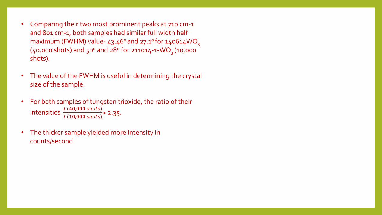
• Comparing their two most prominent peaks at 710 cm-1 and 801 cm-1, both samples had similar full width half maximum (FWHM) value- 43.46o and 27.1o for 140614WO3
(40,000 shots) and 50o and 28o for 211014-1-WO3 (10,000 shots).
• The value of the FWHM is useful in determining the crystal size of the sample.
• For both samples of tungsten trioxide, the ratio of their
intensities 𝐼 (40,000 𝑠ℎ𝑜𝑡𝑠)
𝐼 (10,000 𝑠ℎ𝑜𝑡𝑠)≈ 2.35.
• The thicker sample yielded more intensity in counts/second.

Cyclic voltammetry experiment
Experiment setup
BioLogic VSP Modular 5 channels potentiostat

PRESS PLAY

Bleach
Dye
ECD experiment of ion/electron insertion and extraction

WO3
• Amorphous tungsten oxide recorded multiple cycling.
• The darkness of the color change fades as the cycle progressed.
• HWCVD WO3, MoO3 (40,000 shots) and hybrid samples had a few challenges such as
Irreversibility from colored to bleached state Porous thin film surface (Dissolved in HCl).
Hold time at vertex point: 2 minutes
Applied Bias Electrical Voltage: -2.5 V (reduction) to +3.0
V (Oxidation)
Scan Ewe dE/dt: 100.00mV/s
Irange: 100 mA
Bandwidth: 5- medium
Epa
Epc

Vs
Vs
Cycle 1 ion insertion and bleaching. Cycle 20 ion insertion and bleaching.
Transmittance in electrochromic device increases at as the cycle progressed. The plot shows the difference between the transmittance measured in the first cycle to that of the 20th cycle.

10,000 PLD shots of MoO3
0.02 N vs 0.05 NHCl concentration
(-2V to +2V)
40,000 shots of PLD samples of molybdenum trioxide were not suitable for device fabrication. The surface layer of thin film washed away.
Reasons: Weak interlayer bond and less density of 4.69 g/cm3
Tungsten trioxide = 7.16 g/cm3
8 cycles was recorded for 10,000 shots of MoO3 before coloration began to fade.

Cycle 1 ion insertion and bleaching. Cycle 8 ion insertion and bleaching.
Vs
Vs
10,000 pulsed laser shots of MoO3 thin film used as the working electrode.
(8 cycles were recorded, 0.02 N
HClconcentration
(-2V to +2V)

NON- BLEACHING HWCVD SAMPLES
HWCVD 220914A-WO3 transmittance progress recorded using 0.05 N HCl and -2.5 V potential
As-deposited HWCVD WO3
Colored state- HWCVD WO3
Non-bleaching state HWCVD WO3
Idle HWCVD WO3- Post CV experiment

NON- BLEACHING Hybrid SAMPLES (MoO3/WO3 /MoO3/WO3)
Non-bleaching state Peeling off of the thin film surface layer due to the weak interlayer bond in MoO3

Effect of HCl concentration on optical properties of WO3

WO3
Transmittance of as-deposited thin films (PLD)Comparison of optical properties and potential steps at different HCl conc.

Raman study of thin films post electrochromic cycle

Tungsten trioxide (HWCVD)
Disappearance of monoclinic stretching vibration bands Blue shifts in the bands

PLD tungsten trioxide sample (Post CV)
Disappearance of monoclinic stretching vibration bands at 600 cm-1 range Blue shifts in the bands also. The 700 cm-1 peak broadens and disappears
Before CV- 10,000 PLD
Post CV- 10,000 PLD

Molybdenum trioxide
Forming new peaks and disappearance of prominent peaks at 656 cm-1 and 817 cm-1
Peak at 994.3 cm-1 shifts to right
Before CV- 10,000 PLD
Post CV- 10,000 PLD

Hybrid sample (MoO3/WO3 /MoO3/WO3)- Total of 40,000 shots
o Broad peaks representing the
combination of peaks from both compounds.
---------------------------------o MoO3 at 293.9 cm-1, 342.1 cm-1 and 823.8 cm-1
while 999.5 cm-1 is exclusive to
molybdenum trioxide.---------------------------------o WO3 at 275.7 cm-1, 333.0
cm-1, 811.8 cm-1.---------------------------------o Red shift in peak band
could be identified as the formation of hydrogen
bonding in the structures.
---------------------------------o It is also evidence of
tensile stress in the film.

Conclusions• Electrochromism can be achieved at much lower concentration of 0.02 N and 0.05 N of
hydrochloric acid, as long as sufficient bias potential is passed across the device cause ions and electrons to dissociate and become more mobile.
• Performance of the device is adversely affected by sample thickness especially for porous materials having weak interlayer bonds such as MoO3.
• A better device can be built using HWCVD WO3 by baking the film after deposition to create a more compact structure and possibly a transparent film.
• Transmittance of the device at its colored state is dependent on potential applied. However its not dependent on the concentration of the HCl electrolyte used.
• Raman study shows the formation of hydrogen bonding in the structure of the thin film causing tensile stress and also proves the stretching vibration in the case of WO3 .
• Number of cycles before fading could be enhanced by increasing the value of applied voltage.

THANK YOU
• DR. Mitra (Research advisor)
• DR. Ghosh
• … and all my course mates