ece 448 fpga and asic design with vhdl spring 2008
TRANSCRIPT

ECE 448 FPGA and ASIC Design
with VHDL
Spring 2008

ECE 448 Team
Course Instructor: Kris Gaj [email protected]
Lab Instructors (TAs):
Tuesday & Wednesday sections:Danesh Estekitook ECE 448 in Spring [email protected]
Thursday section: Joe BurnsMS CpE student, specializing inDigital Systems [email protected]
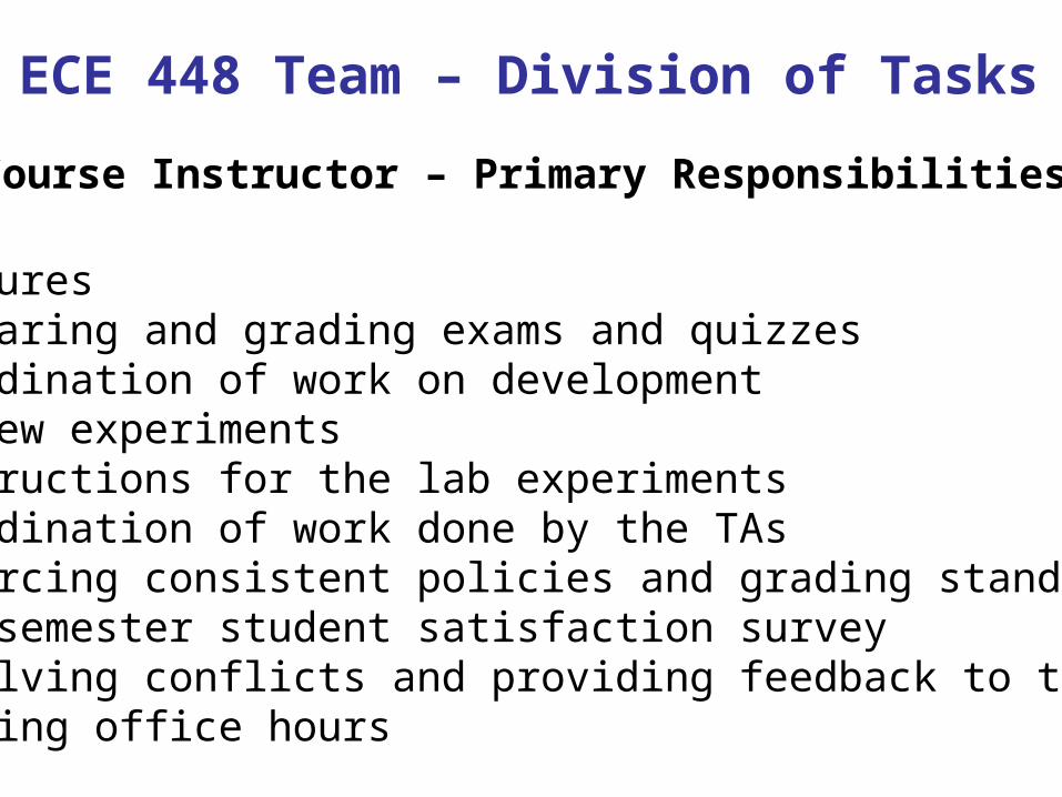
ECE 448 Team – Division of Tasks
Course Instructor – Primary Responsibilities
- Lectures- Preparing and grading exams and quizzes- Coordination of work on development of new experiments- Instructions for the lab experiments- Coordination of work done by the TAs- Enforcing consistent policies and grading standards- Mid-semester student satisfaction survey- Resolving conflicts and providing feedback to the TAs- Holding office hours
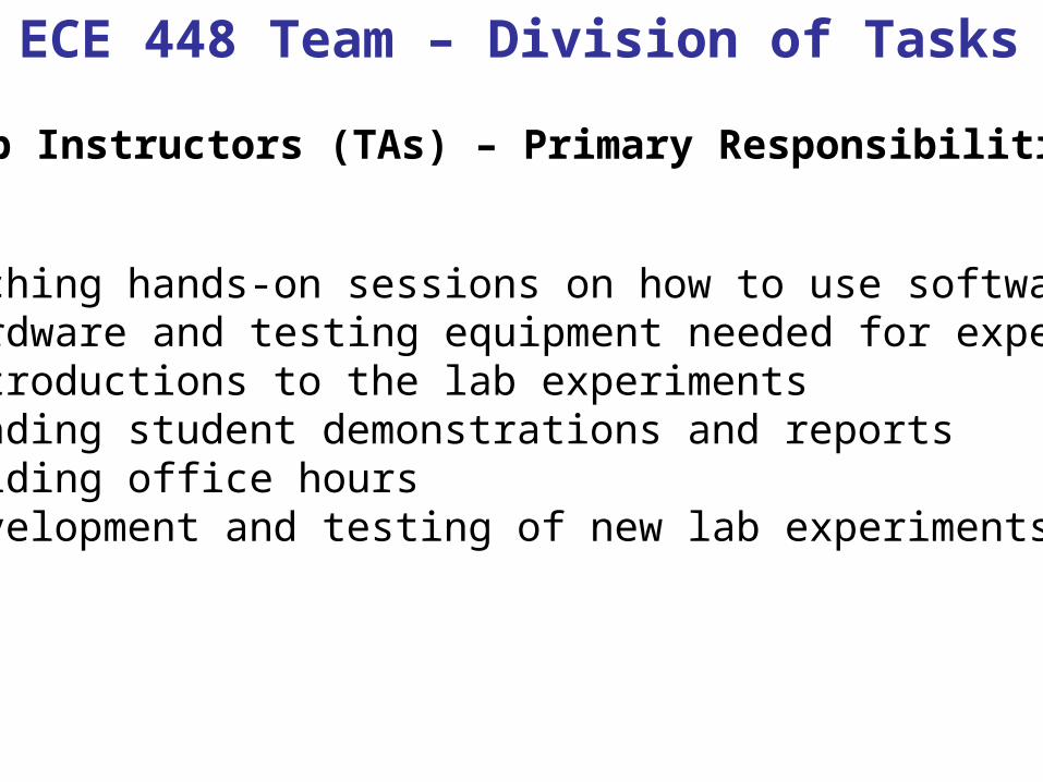
ECE 448 Team – Division of Tasks
Lab Instructors (TAs) – Primary Responsibilities
- Teaching hands-on sessions on how to use software, hardware and testing equipment needed for experiments- Introductions to the lab experiments- Grading student demonstrations and reports- Holding office hours- Development and testing of new lab experiments
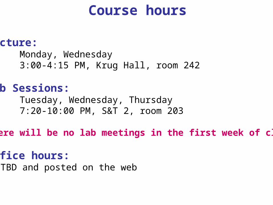
Course hours
Lecture: Monday, Wednesday 3:00-4:15 PM, Krug Hall, room 242
Lab Sessions: Tuesday, Wednesday, Thursday 7:20-10:00 PM, S&T 2, room 203
There will be no lab meetings in the first week of classes
Office hours:TBD and posted on the web

• You are welcome to attend any of the multiple office hour sessions
• Please attend the class meetings of the other section only in case of emergency and give preference in access to the lab computers to the students attending their own section
• All experiment demonstrations need to be done in the presence of your TA, and can be done exclusively during the class time of your section
ECE 448 Section Assignment Rules
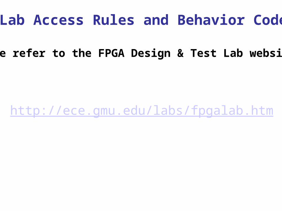
Lab Access Rules and Behavior Code
Please refer to the FPGA Design & Test Lab website:
http://ece.gmu.edu/labs/fpgalab.htm

Grading criteria
First part of the semester (before the Spring break)
Second part of the semester (after the Spring break)
Lab experiments & homework - Part I20%
Final exam25%
Lab experiments & homework - Part II 20%
Midterm exam for the lecture: 10%Midterm exam for the lab: 15%
Quizzes: 5%
Quizzes: 5%
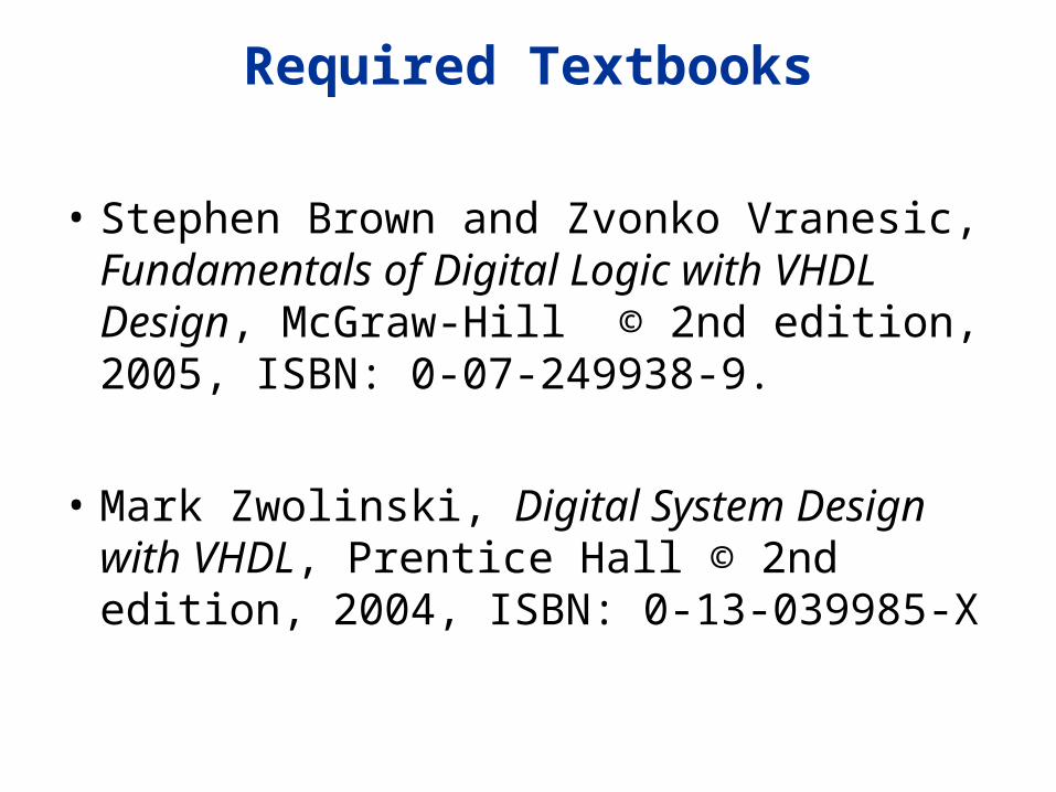
Required Textbooks
• Stephen Brown and Zvonko Vranesic, Fundamentals of Digital Logic with VHDL Design, McGraw-Hill © 2nd edition, 2005, ISBN: 0-07-249938-9.
• Mark Zwolinski, Digital System Design with VHDL, Prentice Hall © 2nd edition, 2004, ISBN: 0-13-039985-X

ECE 331 ECE 332
ECE 280
C
ECE 445
C
ECE 442
ECE 447
C
C
ECE 448
Digital Systems & Computers
PHYS 261 PHYS 265
or
Old Curriculum
C
ECE 492
ECE 493
CS 367
BS EE
BS CpE
Color code:

ECE 331 ECE 332
ECE 280
C
ECE 445
C
ECE 447
C
C
ECE 448
Digital Systems & Computers
PHYS 261 PHYS 265
or
ECE 492
ECE 493
New Curriculum
CS 222 CS 367
BS EE
BS CpE
Color code:
C
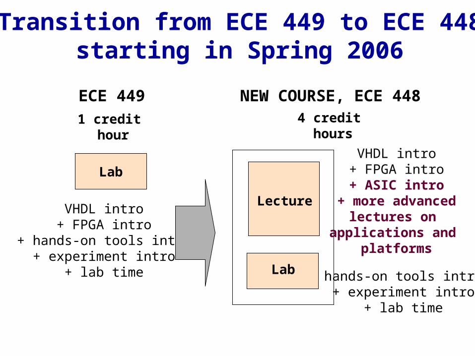
Transition from ECE 449 to ECE 448starting in Spring 2006
ECE 449
1 credit hour
VHDL intro+ FPGA intro
+ hands-on tools intro+ experiment intro
+ lab time
4 credit hours
Lecture
Lab
NEW COURSE, ECE 448
VHDL intro+ FPGA intro+ ASIC intro
+ more advancedlectures on
applications and platforms
hands-on tools intro+ experiment intro
+ lab time
Lab

VHDL:
- writing synthesizable RTL level code in VHDL - writing test benches
FPGAs:
- architecture of FPGA devices - tools for the computer-aided design with FPGAs - current FPGA families & future trends
Topics
ECE 448, FPGA and ASIC Design with VHDL
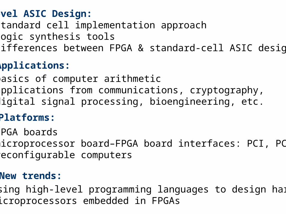
Applications: - basics of computer arithmetic - applications from communications, cryptography, digital signal processing, bioengineering, etc.
- FPGA boards- microprocessor board–FPGA board interfaces: PCI, PCI-X- reconfigurable computers
High-level ASIC Design: - standard cell implementation approach - logic synthesis tools - differences between FPGA & standard-cell ASIC design flow
New trends:- using high-level programming languages to design hardware- microprocessors embedded in FPGAs
Platforms:
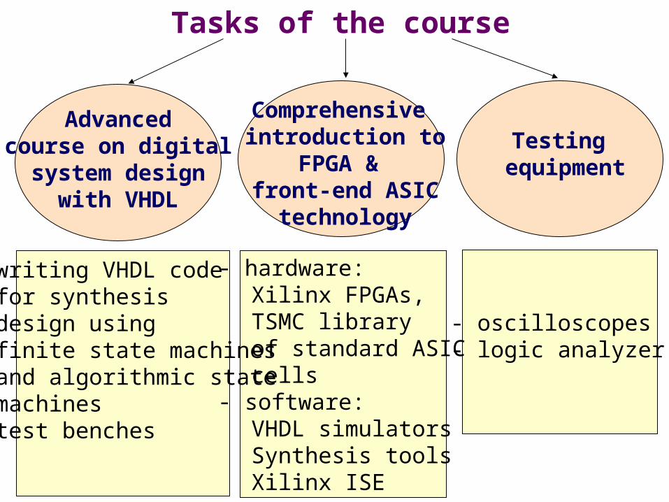
Tasks of the course
Advancedcourse on digital
system designwith VHDL
Comprehensive introduction to
FPGA & front-end ASIC
technology
Testing equipment
- writing VHDL code for synthesis- design using finite state machines and algorithmic state machines- test benches
- hardware:Xilinx FPGAs,TSMC libraryof standard ASICcells
- software:VHDL simulatorsSynthesis toolsXilinx ISE
- oscilloscopes- logic analyzer

VHDL for Specification
VHDL for Simulation
VHDL for Synthesis
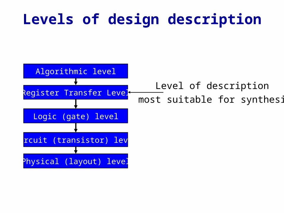
Levels of design description
Algorithmic level
Register Transfer Level
Logic (gate) level
Circuit (transistor) level
Physical (layout) level
Level of description
most suitable for synthesis
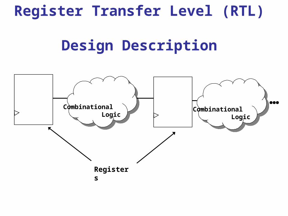
Register Transfer Level (RTL) Design Description
Combinational Logic
Combinational Logic
Registers
…
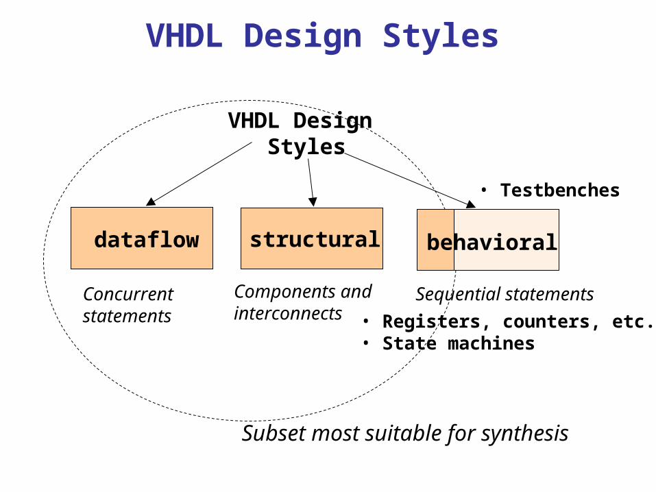
VHDL Design Styles
Components andinterconnects
structural
VHDL Design Styles
dataflow
Concurrent statements
behavioral
• Registers, counters, etc.• State machines
Sequential statements
Subset most suitable for synthesis
• Testbenches

Testbenches
Testbench Environment
TB Processes
Generating
Stimuli
Design Under Test (DUT)
Stimuli All DUT Inputs
Simulated Outputs

World of Integrated Circuits
Integrated Circuits
Full-CustomASICs
Semi-CustomASICs
UserProgrammable
PLD FPGA
PAL PLA PML LUT(Look-Up Table)
MUX Gates
Block R
AM
s
Block R
AM
s
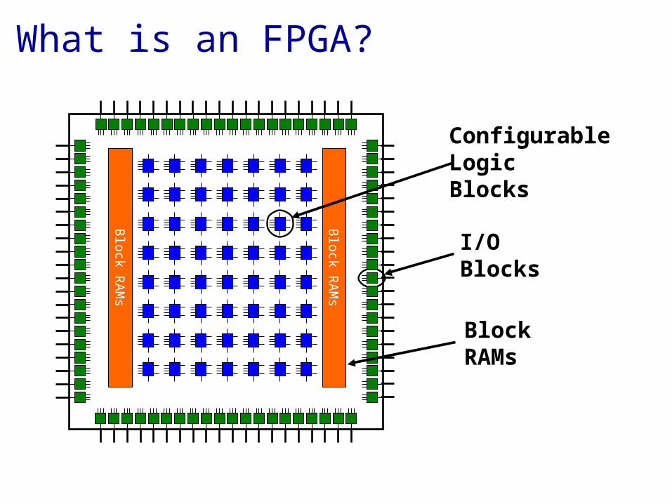
ConfigurableLogicBlocks
I/OBlocks
What is an FPGA?
BlockRAMs
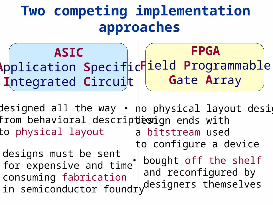
• designs must be sent for expensive and time consuming fabrication in semiconductor foundry
• bought off the shelf and reconfigured by designers themselves
Two competing implementation approaches
ASICApplication Specific
Integrated Circuit
FPGAField Programmable
Gate Array
• designed all the way from behavioral description to physical layout
• no physical layout design; design ends with a bitstream used to configure a device
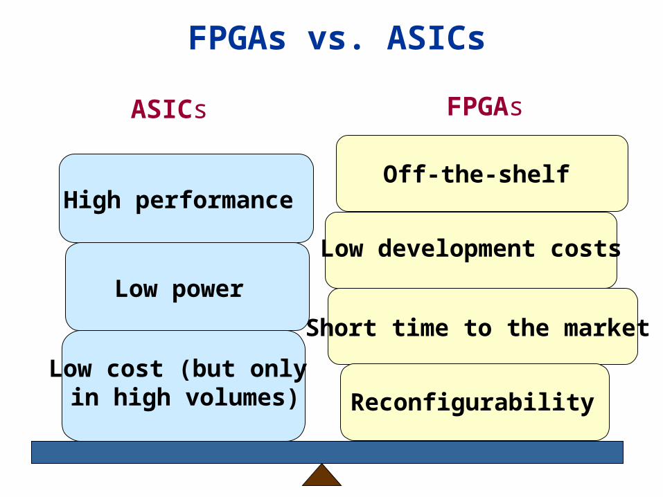
FPGAs vs. ASICs
ASICs FPGAs
High performanceOff-the-shelf
Short time to the market
Low development costs
Reconfigurability
Low power
Low cost (but only in high volumes)
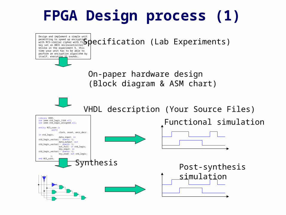
FPGA Design process (1)Design and implement a simple unit permitting to speed up encryption with RC5-similar cipher with fixed key set on 8031 microcontroller. Unlike in the experiment 5, this time your unit has to be able to perform an encryption algorithm by itself, executing 32 rounds…..
Library IEEE;use ieee.std_logic_1164.all;use ieee.std_logic_unsigned.all;
entity RC5_core is port( clock, reset, encr_decr: in std_logic; data_input: in std_logic_vector(31 downto 0); data_output: out std_logic_vector(31 downto 0); out_full: in std_logic; key_input: in std_logic_vector(31 downto 0); key_read: out std_logic; );end AES_core;
Specification (Lab Experiments)
VHDL description (Your Source Files)
Functional simulation
Post-synthesis simulationSynthesis
On-paper hardware design (Block diagram & ASM chart)
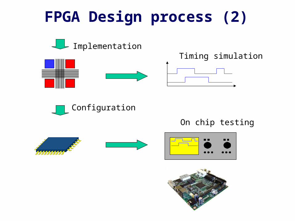
FPGA Design process (2)
Implementation
Configuration
Timing simulation
On chip testing
Simulation Tools
FPGA Synthesis Tools
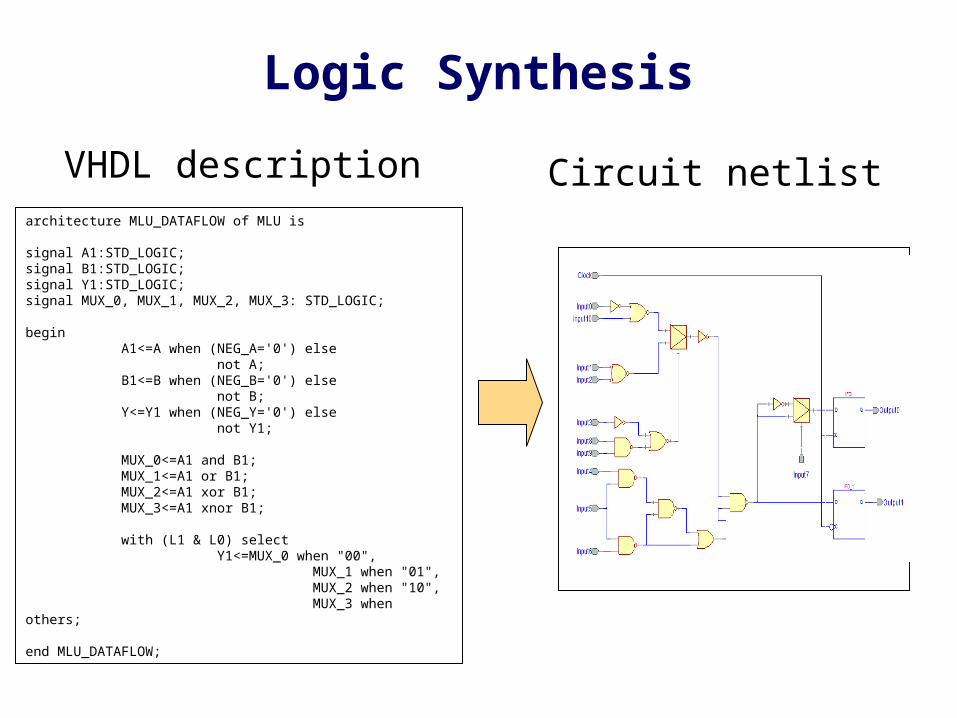
architecture MLU_DATAFLOW of MLU is
signal A1:STD_LOGIC;signal B1:STD_LOGIC;signal Y1:STD_LOGIC;signal MUX_0, MUX_1, MUX_2, MUX_3: STD_LOGIC;
beginA1<=A when (NEG_A='0') else
not A;B1<=B when (NEG_B='0') else
not B;Y<=Y1 when (NEG_Y='0') else
not Y1;
MUX_0<=A1 and B1;MUX_1<=A1 or B1;MUX_2<=A1 xor B1;MUX_3<=A1 xnor B1;
with (L1 & L0) selectY1<=MUX_0 when "00",
MUX_1 when "01",MUX_2 when "10",MUX_3 when others;
end MLU_DATAFLOW;
VHDL description Circuit netlist
Logic Synthesis
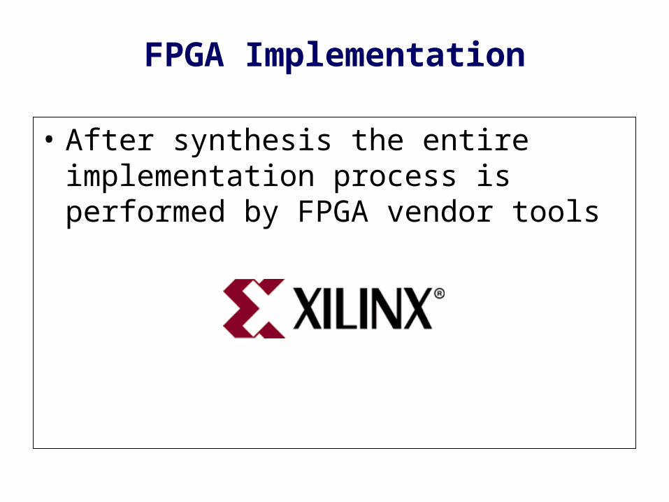
FPGA Implementation
• After synthesis the entire implementation process is performed by FPGA vendor tools
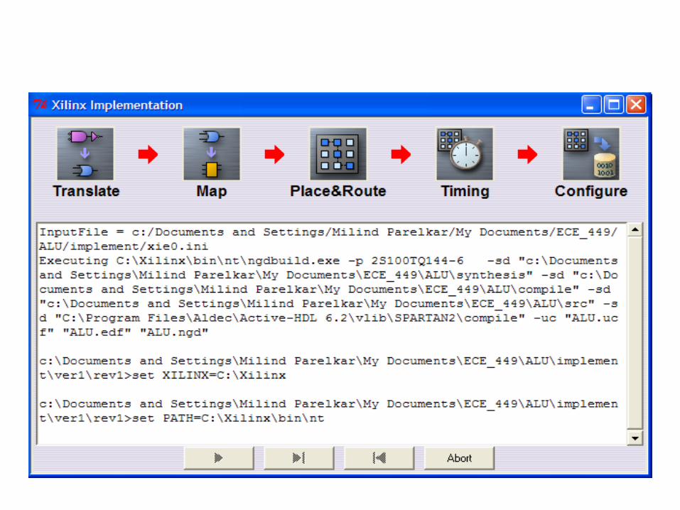

Design Process control from Active-HDL
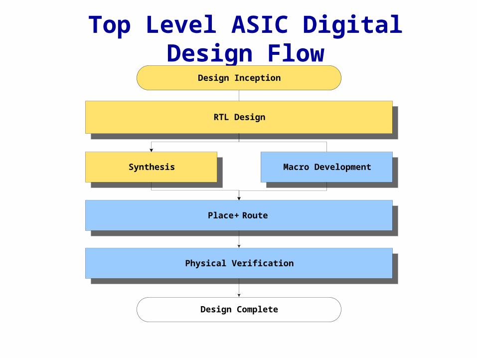
Top Level ASIC Digital Design Flow
RTL Design
Place + Route
Physical Verification
Synthesis
Design Inception
Design Complete
Macro Development

ASIC Simulation Tools

ASIC Synthesis Tools
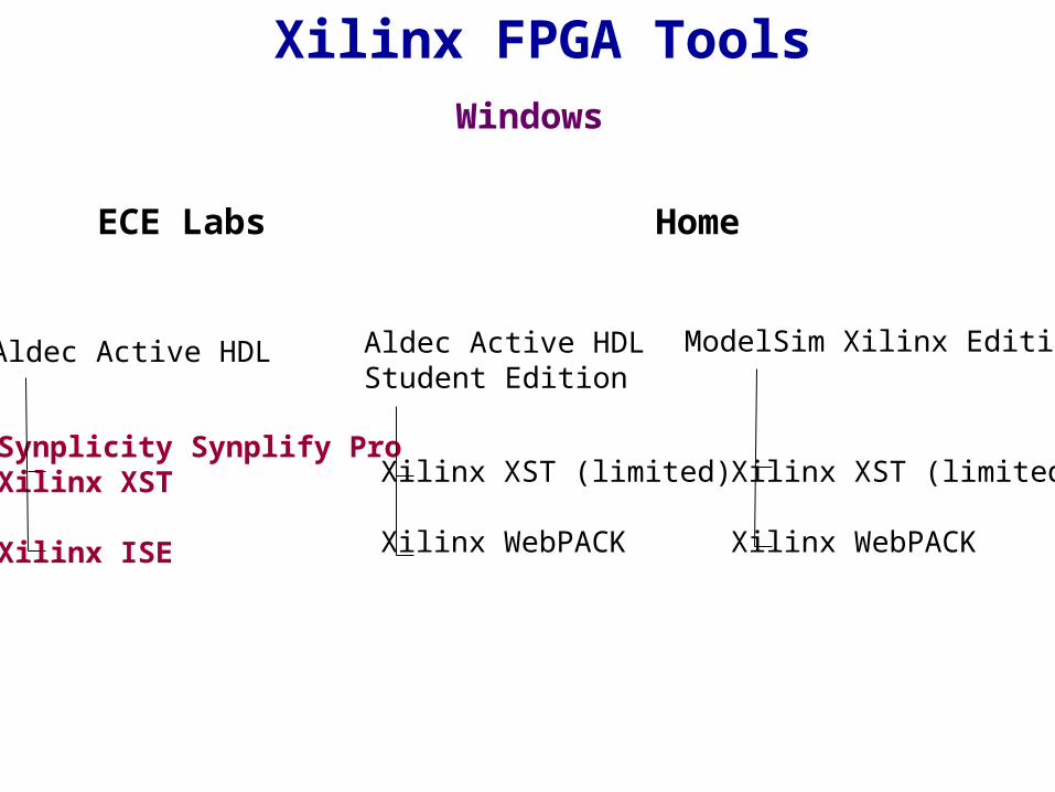
Xilinx FPGA Tools
Aldec Active HDL ModelSim Xilinx Edition
Synplicity Synplify ProXilinx XST
Xilinx ISE
Xilinx XST (limited)
Xilinx WebPACK
ECE Labs Home
Aldec Active HDL Student Edition
Xilinx XST (limited)
Xilinx WebPACK
Windows

Altera FPGA Tools
Altera Quartus II Altera Quartus II
Lab Home for free
Windows

ASIC Tools
Synopsys Design Analyzer remote access
Synopsys Design Analyzer
Lab Home for free
Unix

Celoxica RC10 Educational Board
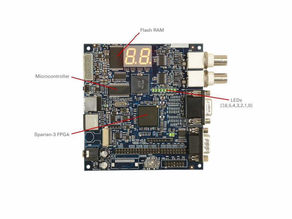
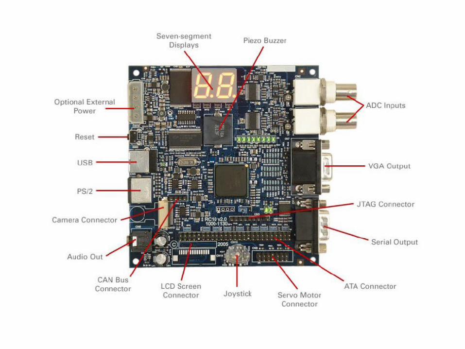
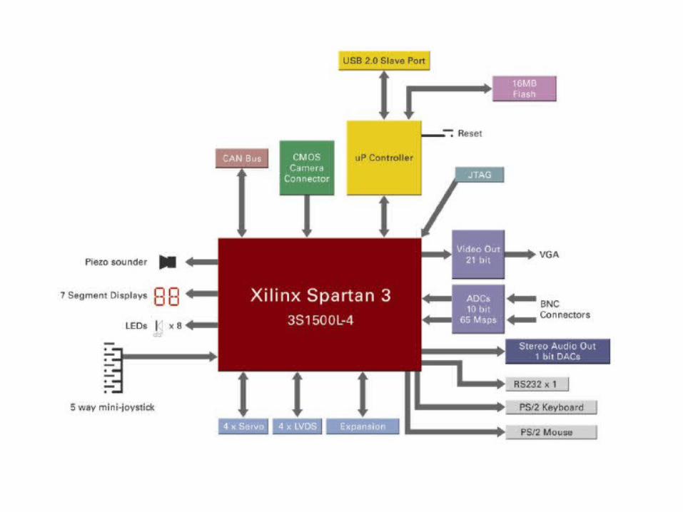
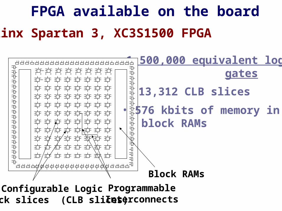
FPGA available on the board
Xilinx Spartan 3, XC3S1500 FPGA
• 1,500,000 equivalent logic gates
• 13,312 CLB slices
ProgrammableInterconnects
Configurable Logic Block slices (CLB slices)
Block RAMs
• 576 kbits of memory in block RAMs

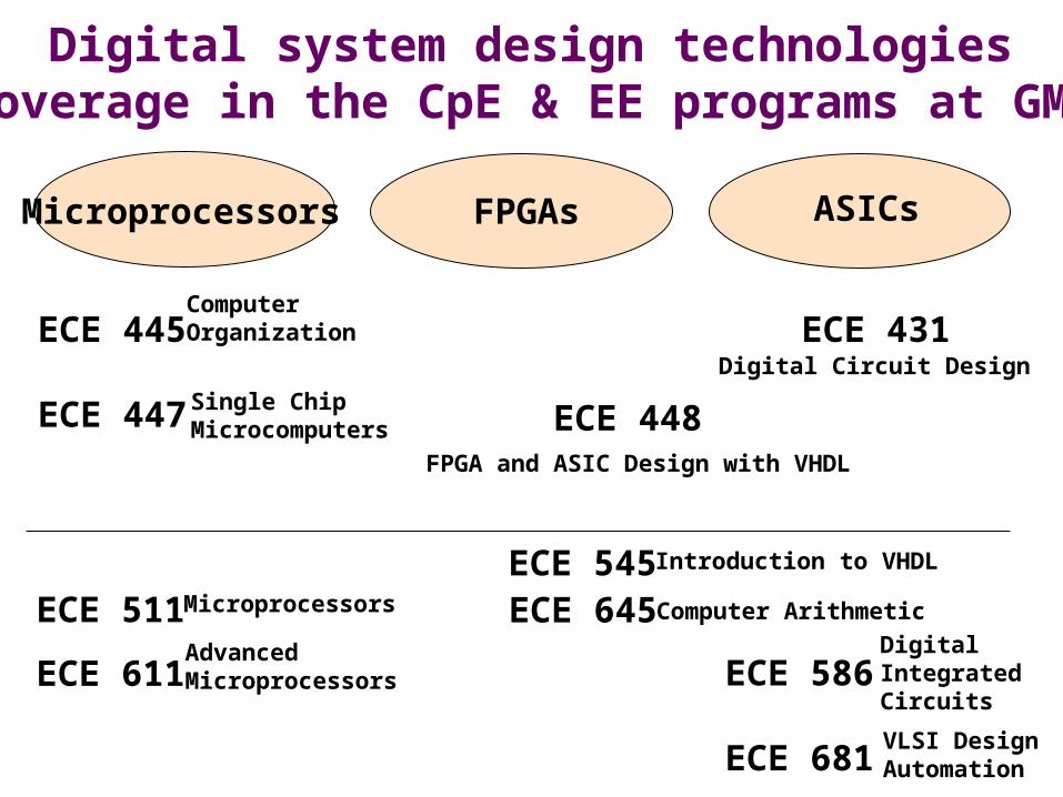
Digital system design technologiescoverage in the CpE & EE programs at GMU
Microprocessors ASICsFPGAs
ECE 445
ECE 447
ECE 586
ECE 681
ECE 448
ECE 511
ECE 611
ECE 431Computer Organization
Single ChipMicrocomputers
FPGA and ASIC Design with VHDL
Digital Circuit Design
Microprocessors
Advanced Microprocessors
Digital Integrated Circuits
VLSI Design Automation
ECE 545 Introduction to VHDL
ECE 645 Computer Arithmetic
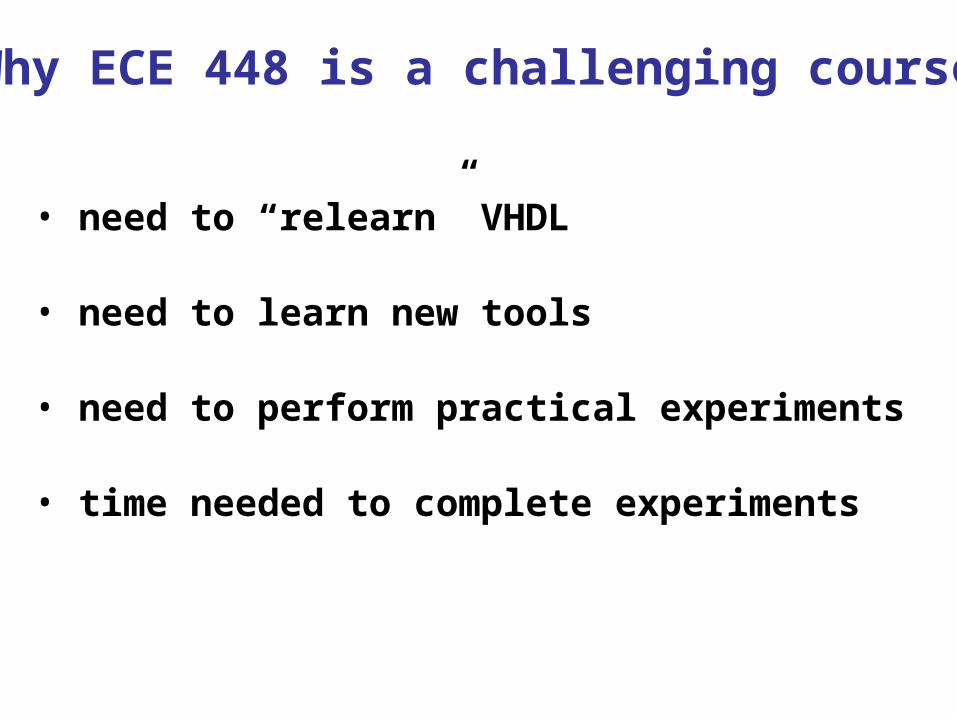
Why ECE 448 is a challenging course?
• need to “relearn” VHDL
• need to learn new tools
• need to perform practical experiments
• time needed to complete experiments
ECE 448: Spring 2006
Student Survey Summary
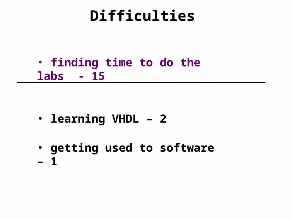
Difficulties
• finding time to do the labs - 15
• learning VHDL – 2
• getting used to software – 1

0
1
2
3
4
5
6
7
8
9
2 6 8 10 15 20 24 30 32 48
Average time spent per one experiment
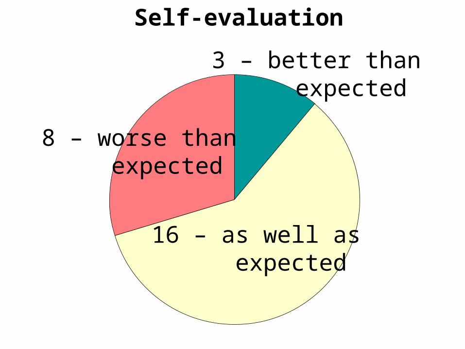
Self-evaluation
8 – worse than expected
16 – as well as expected
3 – better than expected
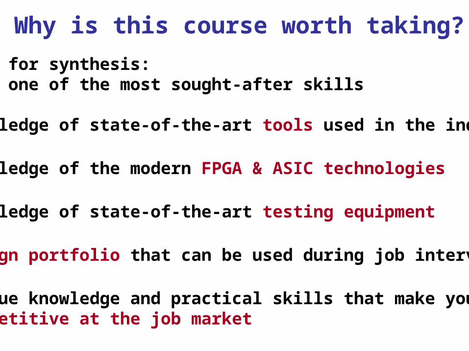
Why is this course worth taking?
• VHDL for synthesis: one of the most sought-after skills
• knowledge of state-of-the-art tools used in the industry
• knowledge of the modern FPGA & ASIC technologies
• knowledge of state-of-the-art testing equipment
• design portfolio that can be used during job interviews
• unique knowledge and practical skills that make you competitive at the job market