ece 448 lecture 5 fpga devices & fpga design flow...ece 448 – fpga and asic design with vhdl 5...
TRANSCRIPT
George Mason University ECE 448 – FPGA and ASIC Design with VHDL
FPGA Devices & FPGA Design Flow
ECE 448 Lecture 5
2 ECE 448 – FPGA and ASIC Design with VHDL
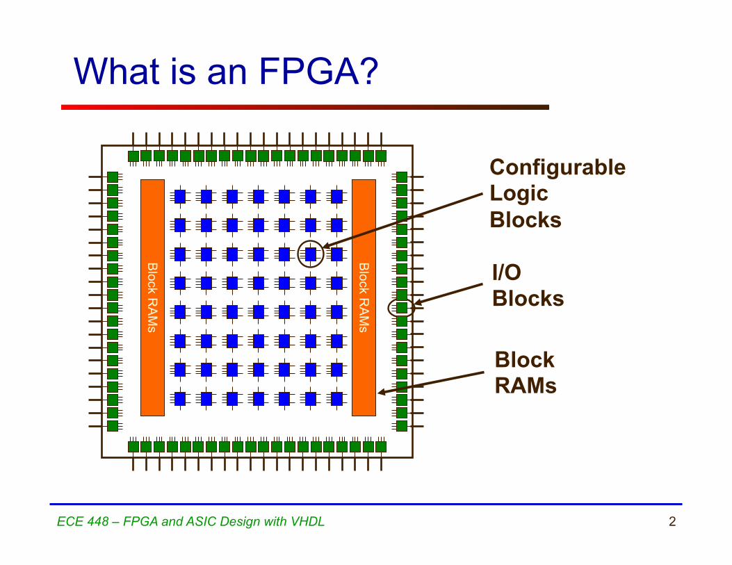
Block R
AM
s
Block R
AM
s
Configurable Logic Blocks
I/O Blocks
What is an FPGA?
Block RAMs
3
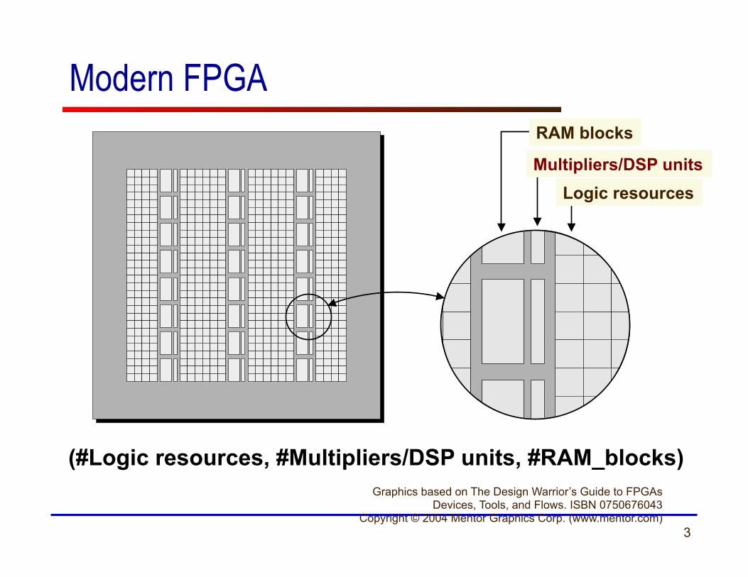
Modern FPGA RAM blocks
Multipliers
Logic blocks
Graphics based on The Design Warrior’s Guide to FPGAs Devices, Tools, and Flows. ISBN 0750676043
Copyright © 2004 Mentor Graphics Corp. (www.mentor.com)
Multipliers/DSP units
RAM blocks
Logic resources
(#Logic resources, #Multipliers/DSP units, #RAM_blocks)
4 ECE 448 – FPGA and ASIC Design with VHDL
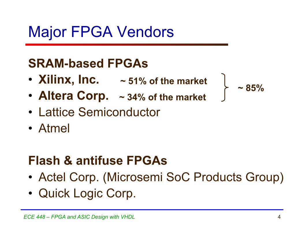
Major FPGA Vendors
SRAM-based FPGAs • Xilinx, Inc. • Altera Corp. • Lattice Semiconductor • Atmel Flash & antifuse FPGAs • Actel Corp. (Microsemi SoC Products Group) • Quick Logic Corp.
~ 51% of the market
~ 34% of the market ~ 85%
5 ECE 448 – FPGA and ASIC Design with VHDL
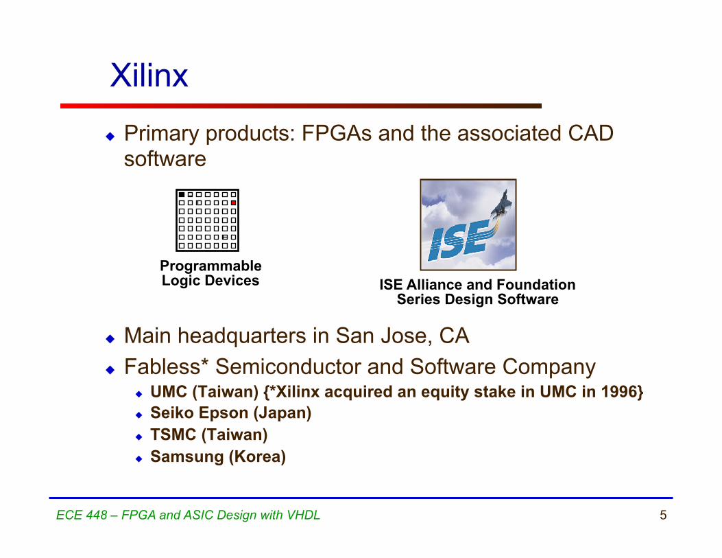
Xilinx u Primary products: FPGAs and the associated CAD
software
u Main headquarters in San Jose, CA u Fabless* Semiconductor and Software Company
u UMC (Taiwan) {*Xilinx acquired an equity stake in UMC in 1996} u Seiko Epson (Japan) u TSMC (Taiwan) u Samsung (Korea)
Programmable Logic Devices ISE Alliance and Foundation
Series Design Software
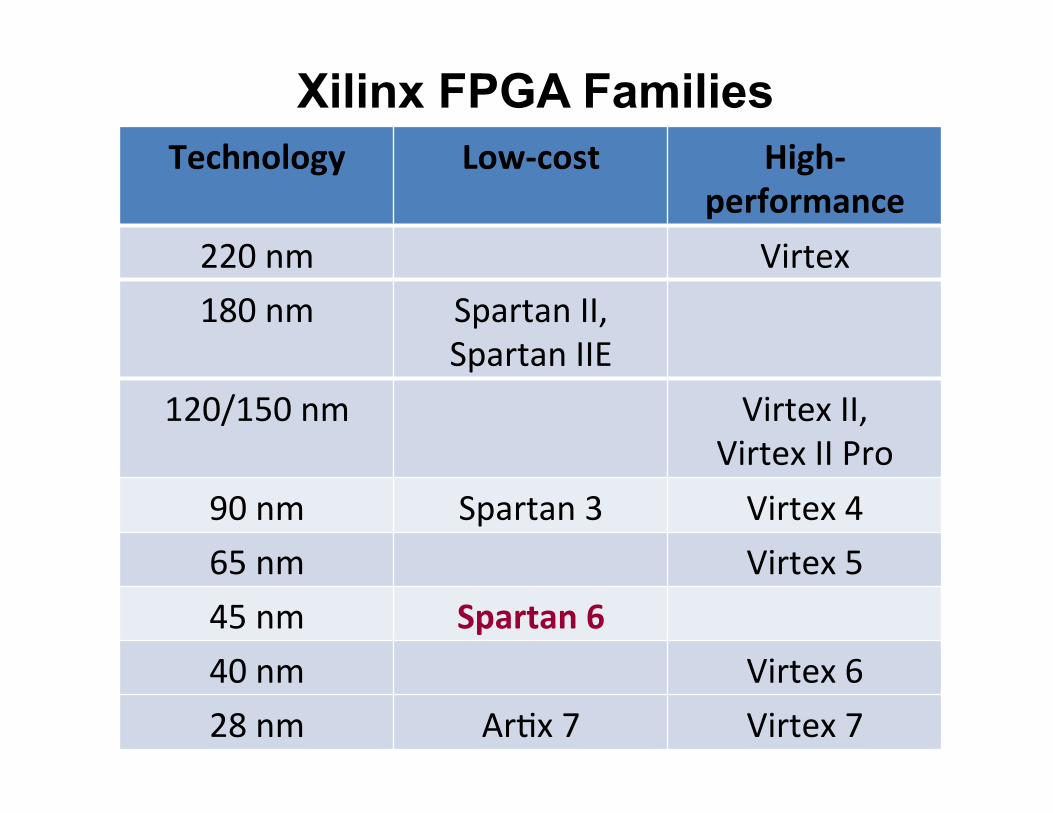
Technology Low-‐cost High-‐performance
220 nm Virtex 180 nm Spartan II,
Spartan IIE 120/150 nm Virtex II,
Virtex II Pro 90 nm Spartan 3 Virtex 4 65 nm Virtex 5 45 nm Spartan 6 40 nm Virtex 6 28 nm Ar=x 7 Virtex 7
Xilinx FPGA Families
7 ECE 448 – FPGA and ASIC Design with VHDL
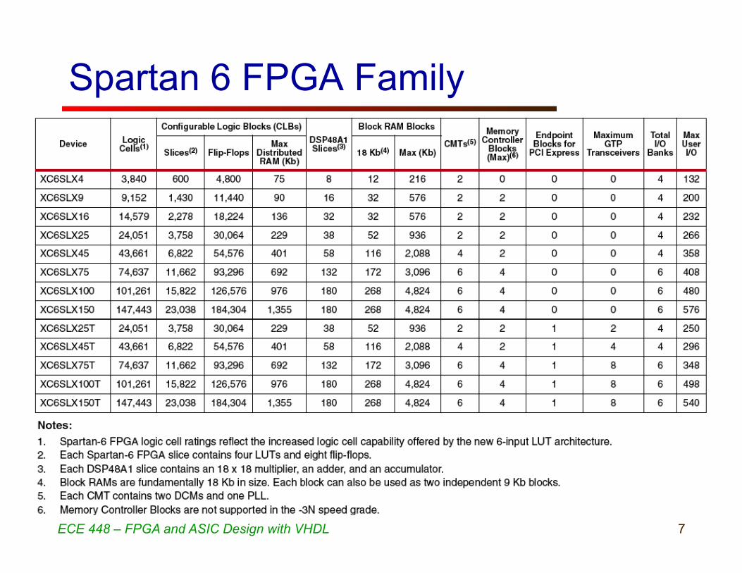
Spartan 6 FPGA Family

George Mason University ECE 448 – FPGA and ASIC Design with VHDL
CLB Structure
9 ECE 448 – FPGA and ASIC Design with VHDL
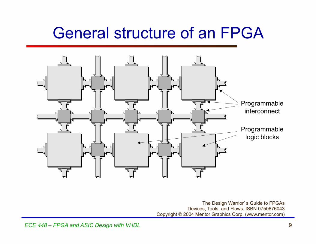
Programmableinterconnect
Programmablelogic blocks
The Design Warrior’s Guide to FPGAs Devices, Tools, and Flows. ISBN 0750676043
Copyright © 2004 Mentor Graphics Corp. (www.mentor.com)
General structure of an FPGA
10 ECE 448 – FPGA and ASIC Design with VHDL
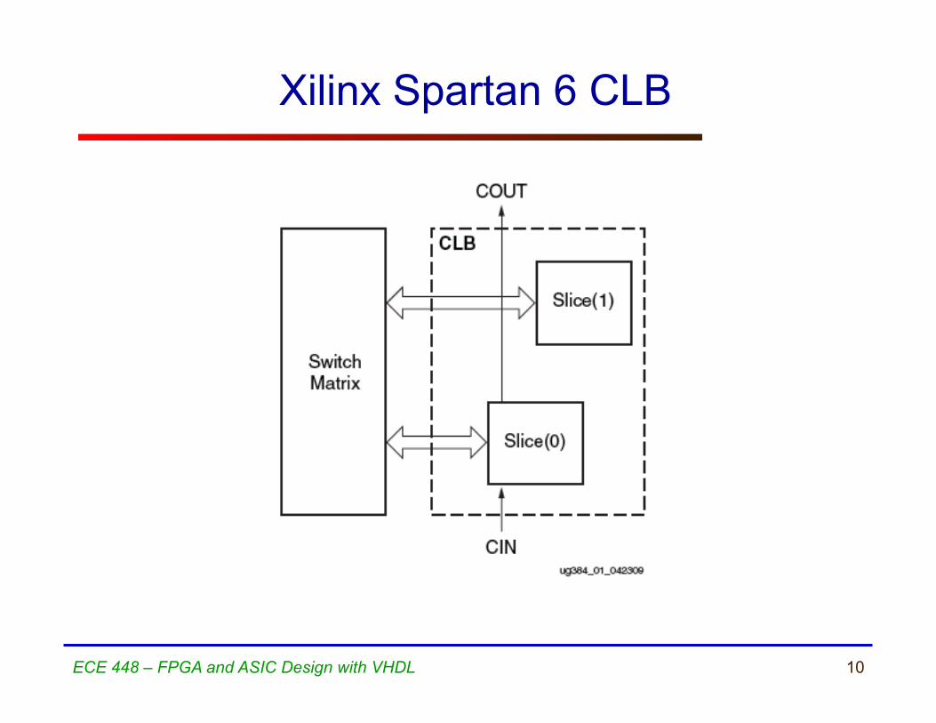
Xilinx Spartan 6 CLB
11 ECE 448 – FPGA and ASIC Design with VHDL
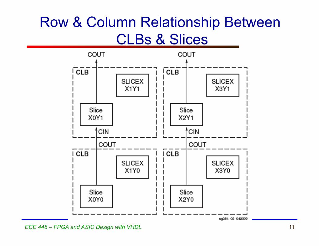
Row & Column Relationship Between CLBs & Slices
12 ECE 448 – FPGA and ASIC Design with VHDL
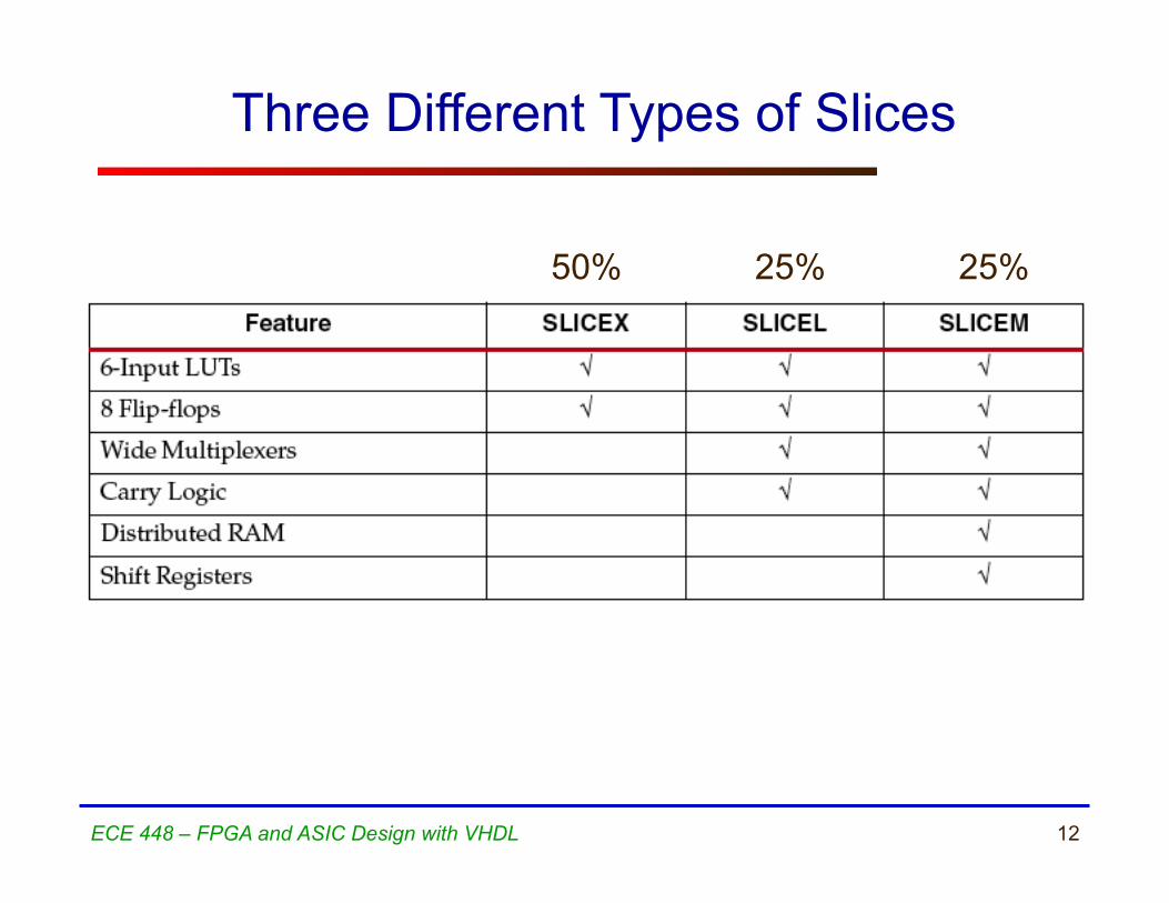
Three Different Types of Slices
50% 25% 25%
13 ECE 448 – FPGA and ASIC Design with VHDL
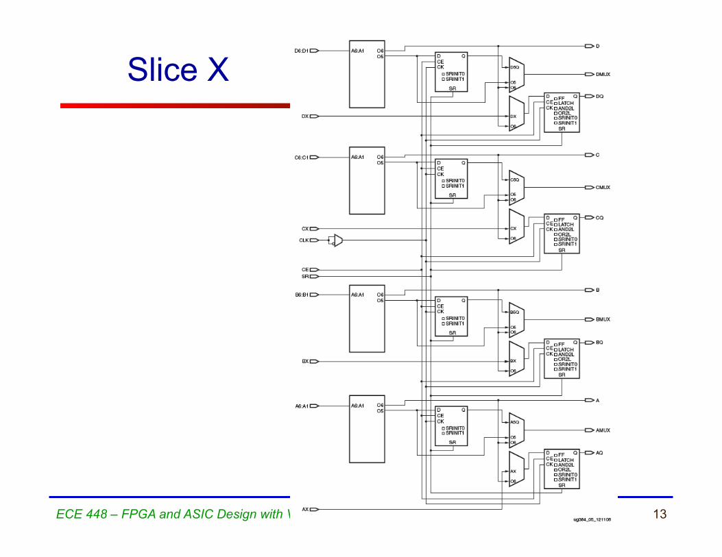
Slice X
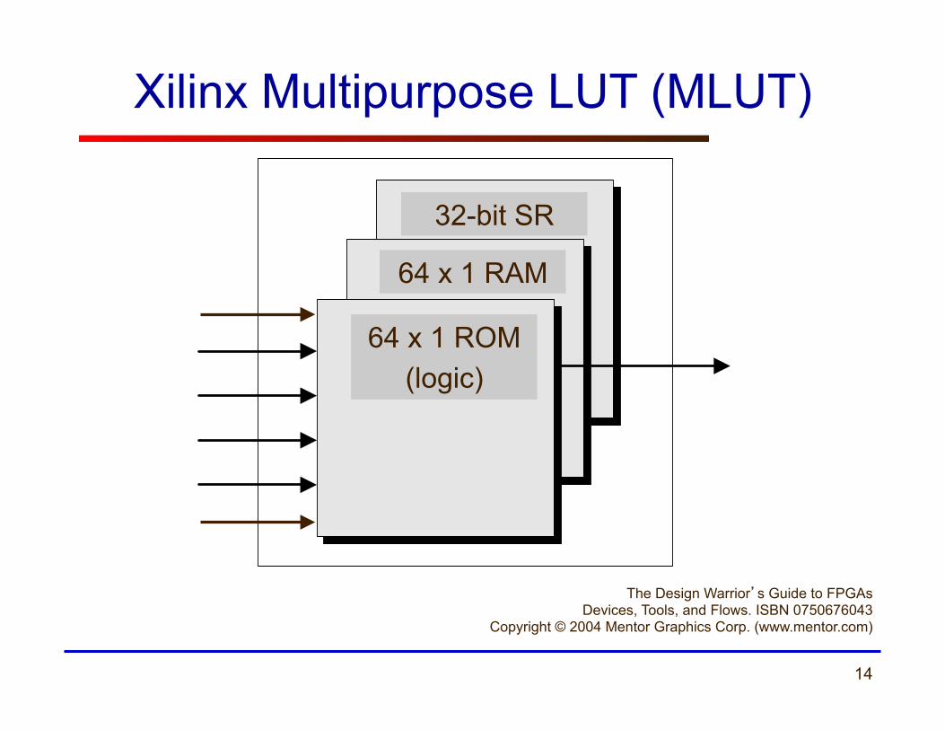
14
16-bit SR
16 x 1 RAM
4-input LUT
The Design Warrior’s Guide to FPGAs Devices, Tools, and Flows. ISBN 0750676043
Copyright © 2004 Mentor Graphics Corp. (www.mentor.com)
Xilinx Multipurpose LUT (MLUT)
64 x 1 ROM (logic)
64 x 1 RAM
32-bit SR

15 ECE 448 – FPGA and ASIC Design with VHDL
4-input LUT (Look-Up Table) in the Basic ROM Mode
• Look-Up tables are primary elements for logic implementation
• Each LUT can implement any function of 4 inputs
x1 x2 x3 x4
y
x1 x2
y
LUT
x1x2x3x4
y
0x1
0x2 x3 x4
0 00 0 0 10 0 1 00 0 1 10 1 0 00 1 0 10 1 1 00 1 1 11 0 0 01 0 0 11 0 1 01 0 1 11 1 0 01 1 0 11 1 1 01 1 1 1
y0100010101001100
0x1
0x2 x3 x4
0 00 0 0 10 0 1 00 0 1 10 1 0 00 1 0 10 1 1 00 1 1 11 0 0 01 0 0 11 0 1 01 0 1 11 1 0 01 1 0 11 1 1 01 1 1 1
y1111111111110000
x1 x2 x3 x4
y
x1 x2 x3 x4
y
x1 x2
y
x1 x2
y
LUT
x1x2x3x4
y
0x1
0x2 x3 x4
0 00 0 0 10 0 1 00 0 1 10 1 0 00 1 0 10 1 1 00 1 1 11 0 0 01 0 0 11 0 1 01 0 1 11 1 0 01 1 0 11 1 1 01 1 1 1
y0100010101001100
0x1
0x2 x3 x4
0 00 0 0 10 0 1 00 0 1 10 1 0 00 1 0 10 1 1 00 1 1 11 0 0 01 0 0 11 0 1 01 0 1 11 1 0 01 1 0 11 1 1 01 1 1 1
y0100010101001100
0x1
0x2 x3 x4
0 00 0 0 10 0 1 00 0 1 10 1 0 00 1 0 10 1 1 00 1 1 11 0 0 01 0 0 11 0 1 01 0 1 11 1 0 01 1 0 11 1 1 01 1 1 1
y1111111111110000
0x1
0x2 x3 x4
0 00 0 0 10 0 1 00 0 1 10 1 0 00 1 0 10 1 1 00 1 1 11 0 0 01 0 0 11 0 1 01 0 1 11 1 0 01 1 0 11 1 1 01 1 1 1
y1111111111110000
16 ECE 448 – FPGA and ASIC Design with VHDL
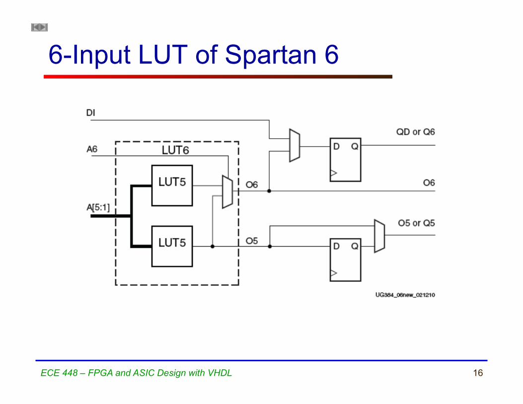
6-Input LUT of Spartan 6
17
18 ECE 448 – FPGA and ASIC Design with VHDL
Reset and Set Configurations
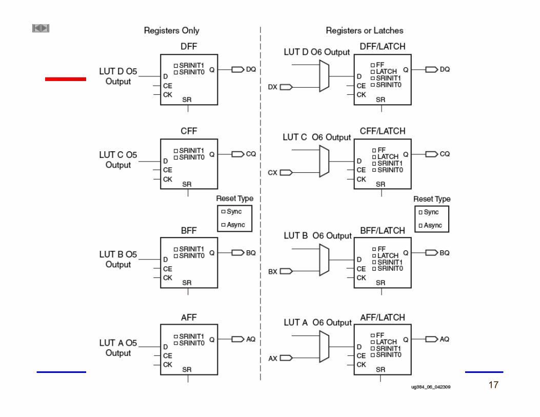
• No set or reset • Synchronous set • Synchronous reset • Asynchronous set (preset) • Asynchronous reset (clear)
19 ECE 448 – FPGA and ASIC Design with VHDL
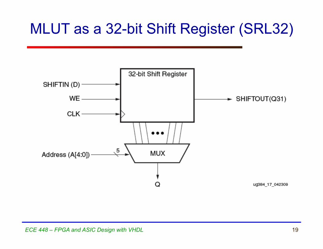
MLUT as a 32-bit Shift Register (SRL32)
George Mason University ECE 448 – FPGA and ASIC Design with VHDL
Input/Output Blocks (IOBs)
21 ECE 448 – FPGA and ASIC Design with VHDL
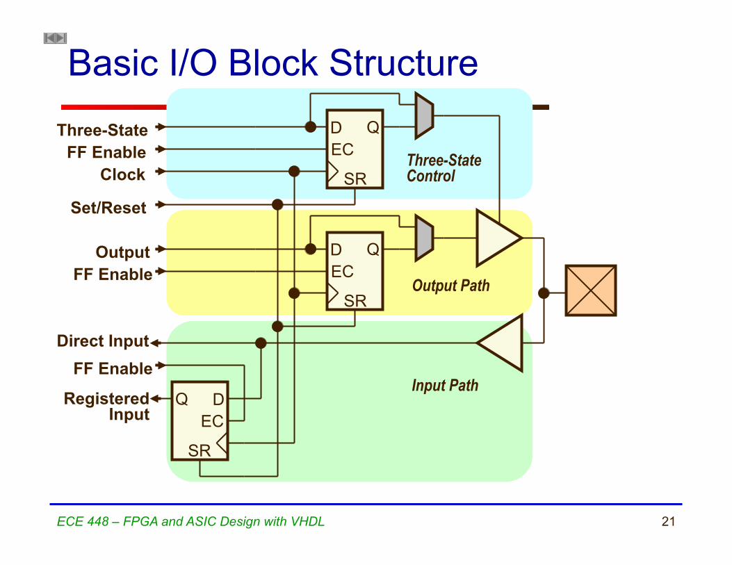
Basic I/O Block Structure
D EC
Q
SR
D EC
Q
SR
D EC
Q
SR
Three-State Control
Output Path
Input Path
Three-State
Output
Clock
Set/Reset
Direct Input
Registered Input
FF Enable
FF Enable
FF Enable
22 ECE 448 – FPGA and ASIC Design with VHDL
IOB Functionality
• IOB provides interface between the package pins and CLBs
• Each IOB can work as uni- or bi-directional I/O
• Outputs can be forced into High Impedance • Inputs and outputs can be registered
• advised for high-performance I/O • Inputs can be delayed
George Mason University ECE 448 – FPGA and ASIC Design with VHDL
Clock Management
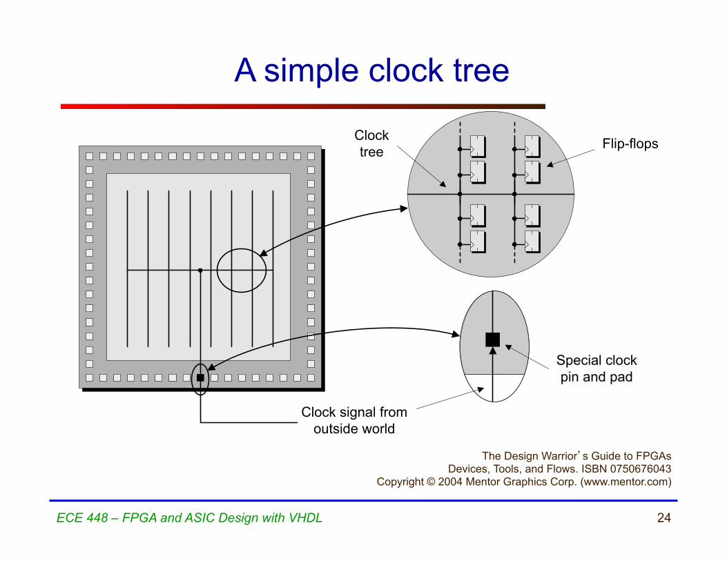
24 ECE 448 – FPGA and ASIC Design with VHDL
Clock signal fromoutside world
Clocktree Flip-flops
Special clockpin and pad
A simple clock tree
The Design Warrior’s Guide to FPGAs Devices, Tools, and Flows. ISBN 0750676043
Copyright © 2004 Mentor Graphics Corp. (www.mentor.com)
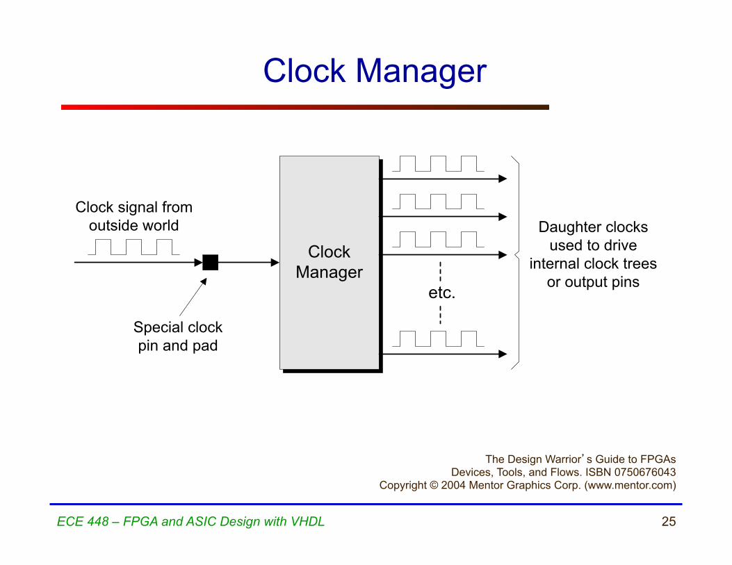
25 ECE 448 – FPGA and ASIC Design with VHDL
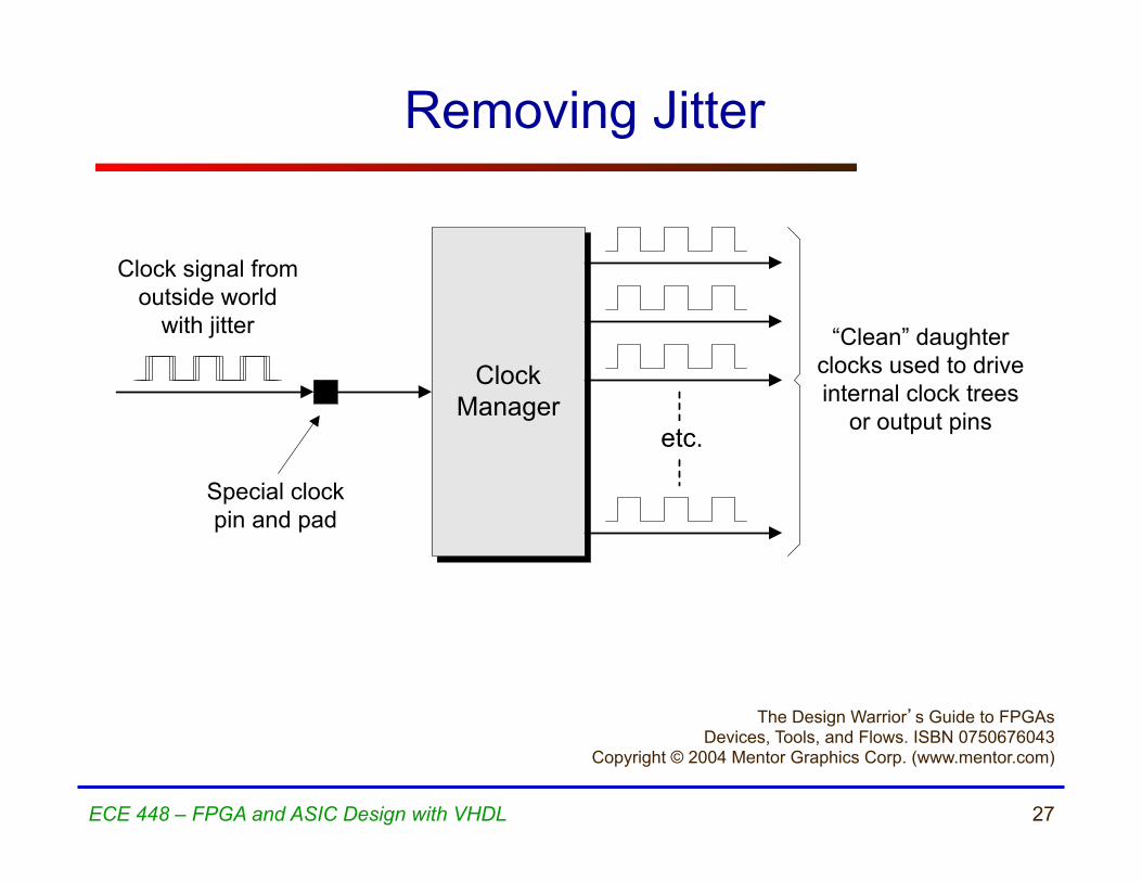
Clock signal fromoutside world
Special clockpin and pad
Daughter clocksused to drive
internal clock treesor output pins
ClockManager
etc.
The Design Warrior’s Guide to FPGAs Devices, Tools, and Flows. ISBN 0750676043
Copyright © 2004 Mentor Graphics Corp. (www.mentor.com)
Clock Manager
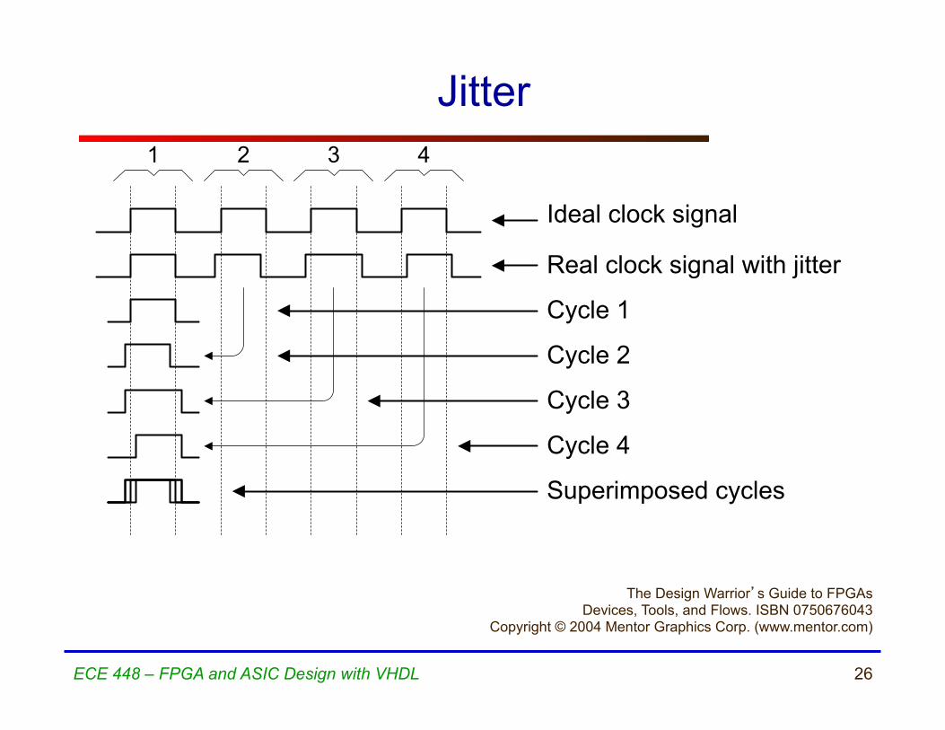
26 ECE 448 – FPGA and ASIC Design with VHDL
Ideal clock signal
1 2 3 4
Real clock signal with jitter
Cycle 1
Cycle 2
Cycle 3
Cycle 4
Superimposed cycles
The Design Warrior’s Guide to FPGAs Devices, Tools, and Flows. ISBN 0750676043
Copyright © 2004 Mentor Graphics Corp. (www.mentor.com)
Jitter
27 ECE 448 – FPGA and ASIC Design with VHDL
Clock signal fromoutside world
with jitter
Special clockpin and pad
“Clean” daughterclocks used to driveinternal clock trees
or output pins
ClockManager
etc.
The Design Warrior’s Guide to FPGAs Devices, Tools, and Flows. ISBN 0750676043
Copyright © 2004 Mentor Graphics Corp. (www.mentor.com)
Removing Jitter
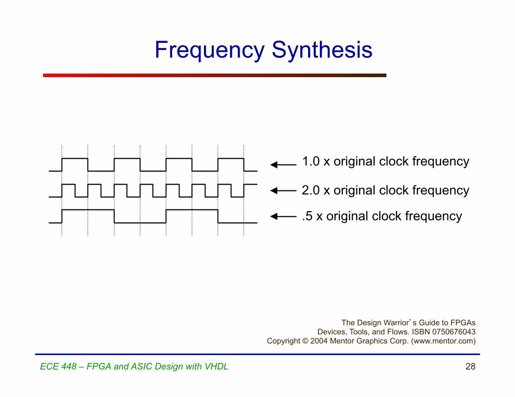
28 ECE 448 – FPGA and ASIC Design with VHDL
1.0 x original clock frequency
2.0 x original clock frequency
.5 x original clock frequency
The Design Warrior’s Guide to FPGAs Devices, Tools, and Flows. ISBN 0750676043
Copyright © 2004 Mentor Graphics Corp. (www.mentor.com)
Frequency Synthesis
29 ECE 448 – FPGA and ASIC Design with VHDL
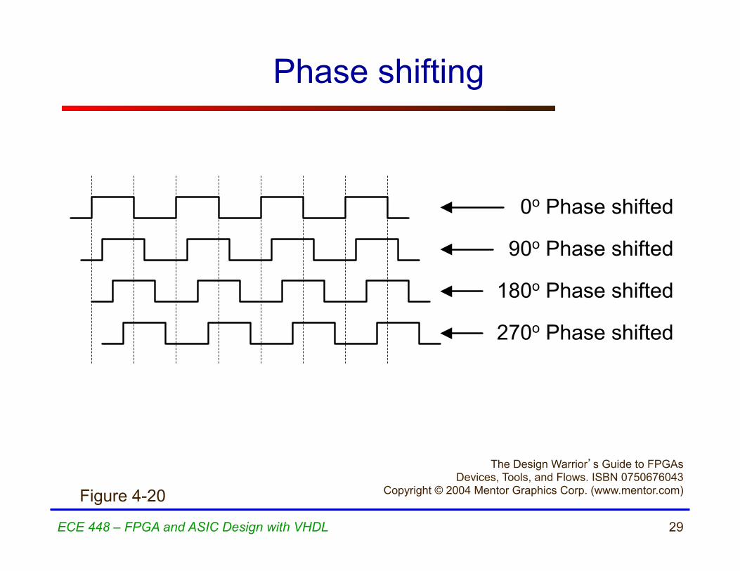
Figure 4-20
0o Phase shifted
90o Phase shifted
180o Phase shifted
270o Phase shifted
The Design Warrior’s Guide to FPGAs Devices, Tools, and Flows. ISBN 0750676043
Copyright © 2004 Mentor Graphics Corp. (www.mentor.com)
Phase shifting
30 ECE 448 – FPGA and ASIC Design with VHDL
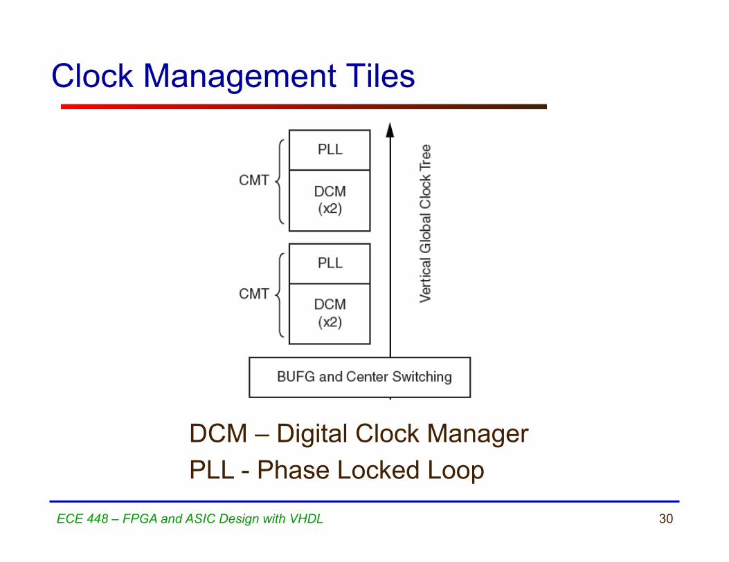
DCM – Digital Clock Manager PLL - Phase Locked Loop
Clock Management Tiles
George Mason University ECE 448 – FPGA and ASIC Design with VHDL
Spartan-6 Family Attributes
32 ECE 448 – FPGA and ASIC Design with VHDL
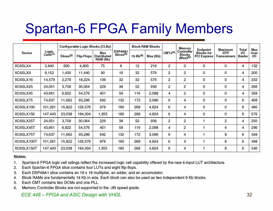
Spartan-6 FPGA Family Members
33 ECE 448 – FPGA and ASIC Design with VHDL
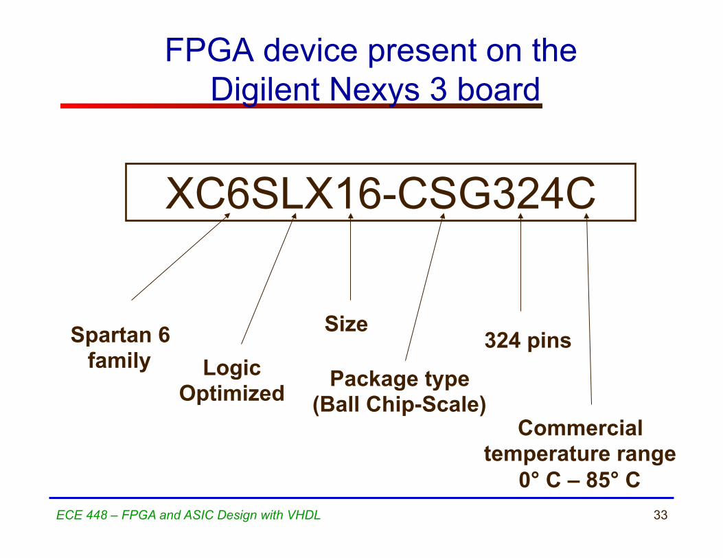
FPGA device present on the Digilent Nexys 3 board
XC6SLX16-CSG324C
Spartan 6 family
Size 324 pins
Package type (Ball Chip-Scale)
Commercial temperature range
0° C – 85° C
Logic Optimized
George Mason University
FPGA Design Flow
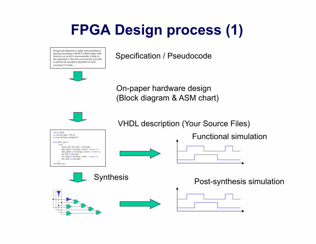
FPGA Design process (1) Design and implement a simple unit permitting to speed up encryption with RC5-similar cipher with fixed key set on 8031 microcontroller. Unlike in the experiment 5, this time your unit has to be able to perform an encryption algorithm by itself, executing 32 rounds…..
Library IEEE; use ieee.std_logic_1164.all; use ieee.std_logic_unsigned.all; entity RC5_core is port( clock, reset, encr_decr: in std_logic; data_input: in std_logic_vector(31 downto 0); data_output: out std_logic_vector(31 downto 0); out_full: in std_logic; key_input: in std_logic_vector(31 downto 0); key_read: out std_logic; ); end AES_core;
Specification / Pseudocode
VHDL description (Your Source Files) Functional simulation
Post-synthesis simulation Synthesis
On-paper hardware design (Block diagram & ASM chart)
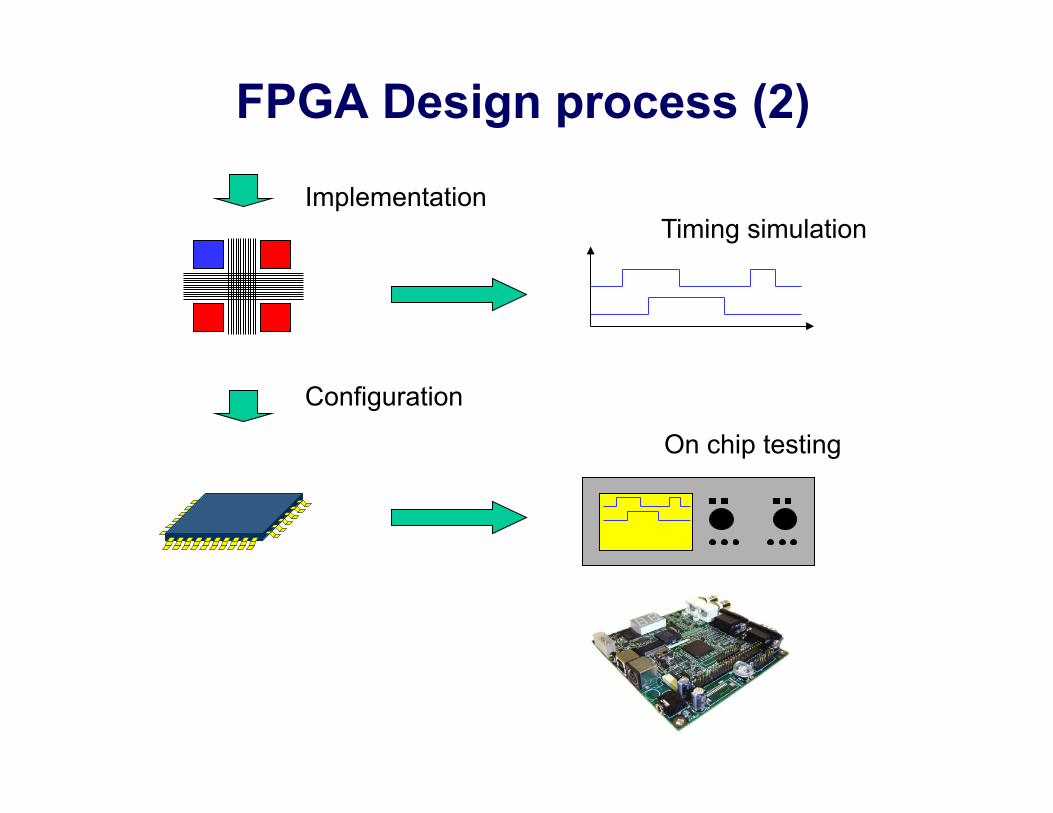
FPGA Design process (2)
Implementation
Configuration
Timing simulation
On chip testing

37
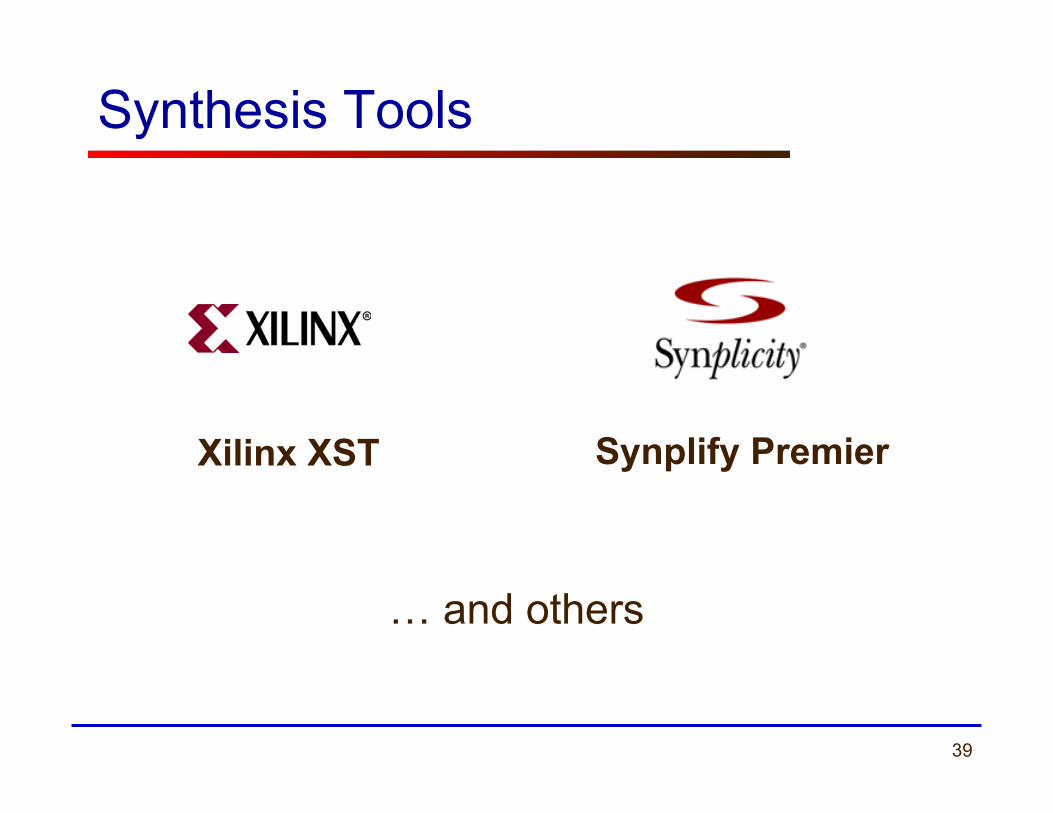
Tools used in FPGA Design Flow
Xilinx XST
Design
Synthesis
Implementation
Xilinx ISE
VHDL code
Netlist
Bitstream
Synplify Premier
Functionally verified
VHDL code
George Mason University
Synthesis
39
Synthesis Tools
… and others
Synplify Premier Xilinx XST
40
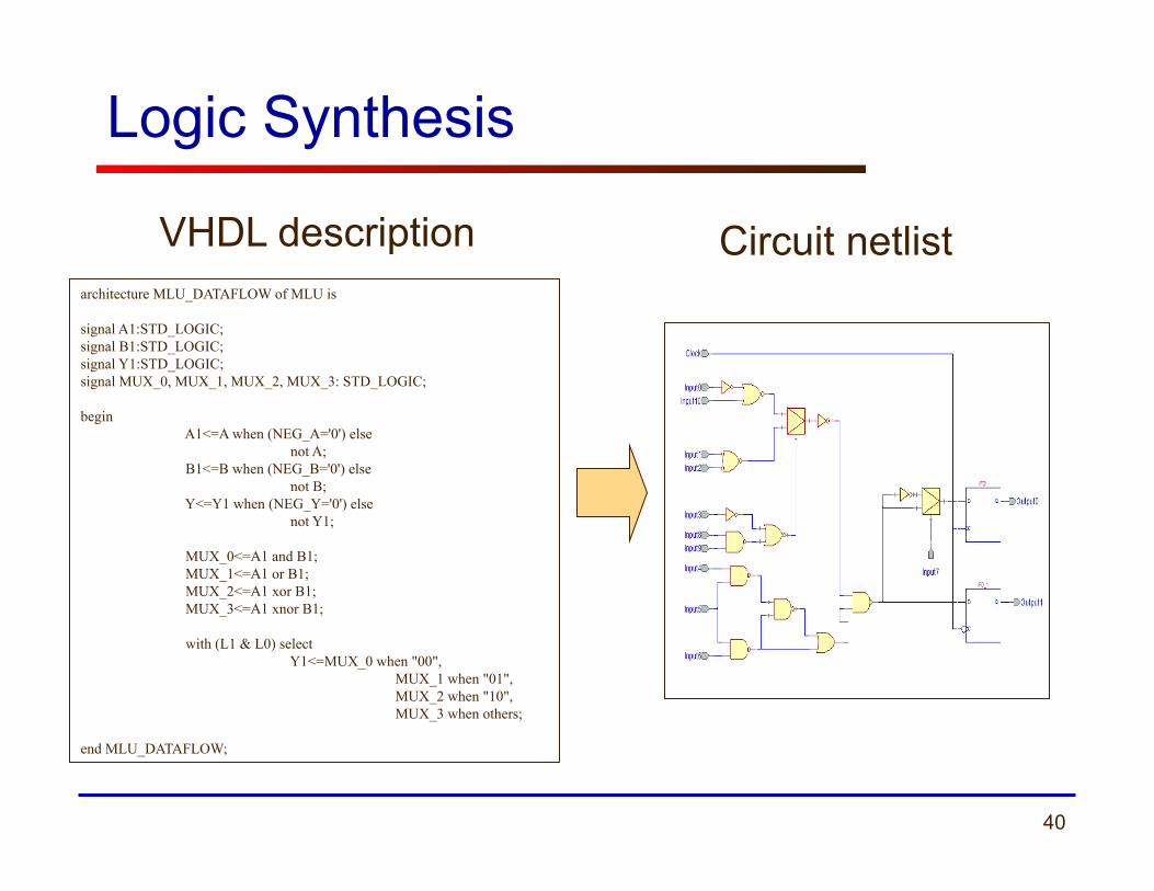
architecture MLU_DATAFLOW of MLU is
signal A1:STD_LOGIC; signal B1:STD_LOGIC; signal Y1:STD_LOGIC; signal MUX_0, MUX_1, MUX_2, MUX_3: STD_LOGIC; begin
A1<=A when (NEG_A='0') else not A; B1<=B when (NEG_B='0') else not B; Y<=Y1 when (NEG_Y='0') else not Y1; MUX_0<=A1 and B1; MUX_1<=A1 or B1; MUX_2<=A1 xor B1; MUX_3<=A1 xnor B1; with (L1 & L0) select Y1<=MUX_0 when "00", MUX_1 when "01", MUX_2 when "10", MUX_3 when others;
end MLU_DATAFLOW;
VHDL description Circuit netlist
Logic Synthesis
41
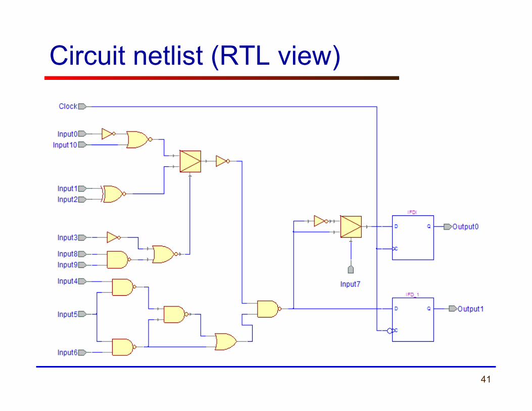
Circuit netlist (RTL view)
42
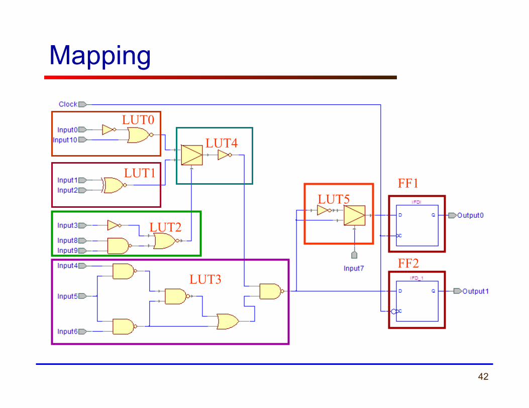
Mapping
LUT2
LUT3
LUT4
LUT5
LUT1 FF1
FF2
LUT0
43
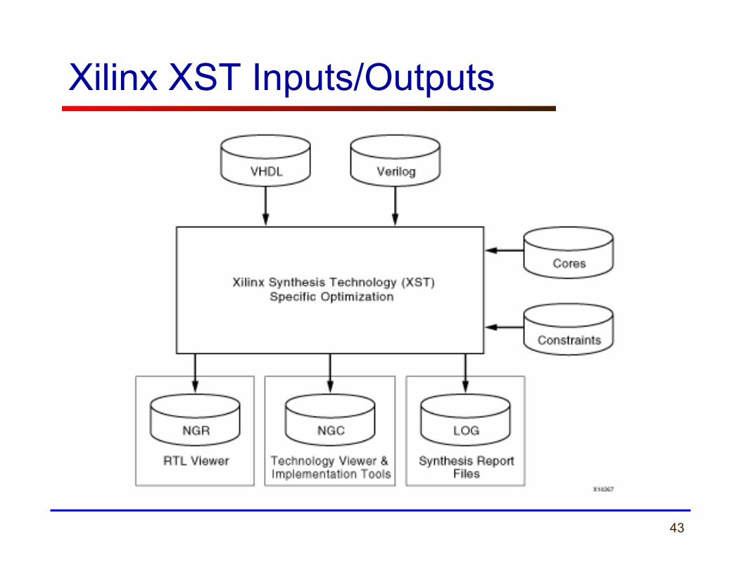
Xilinx XST Inputs/Outputs
44
Xilinx XST Inputs
• RTL VHDL and/or Verilog files • Constraints – XCF
Xilinx constraints file in which you can specify synthesis, timing, and specific implementation constraints that can be propagated to the NGC file.
• Core files These files can be in either NGC or EDIF format. XST does not modify cores. It uses them to inform area and timing optimization surrounding the cores.
45
Xilinx XST Outputs • NGC
Netlist file with constraint information • NGR
This is a schematic representation of the pre-optimized design shown at the Register Transfer Level (RTL). This representation is in terms of generic symbols, such as adders, multipliers, counters, AND gates, and OR gates, and is generated after the HDL synthesis phase of the synthesis process.
• LOG This report contains the results from the synthesis run, including area and timing estimation.
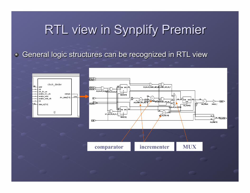
RTL view in Synplify Premier
incrementer comparator
" General logic structures can be recognized in RTL view
MUX
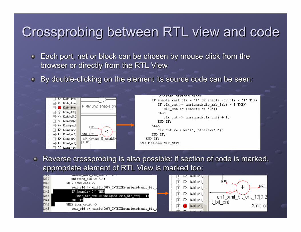
Crossprobing between RTL view and code " Each port, net or block can be chosen by mouse click from the
browser or directly from the RTL View
" By double-clicking on the element its source code can be seen:
" Reverse crossprobing is also possible: if section of code is marked, appropriate element of RTL View is marked too:

Technology View in Synplify Pro
" Technology view is a mapped RTL view. It can be seen by pressing button or by double-click on “.srm” file
" As in case of “RTL View”, buttons can be used here
" Two additional buttons are enabled: - show critical path - open timing analyst
Technology view is presented using device primitives Ports, nets and
blocks browser
Pay attention: technology view is usually large and presented on number of sheets
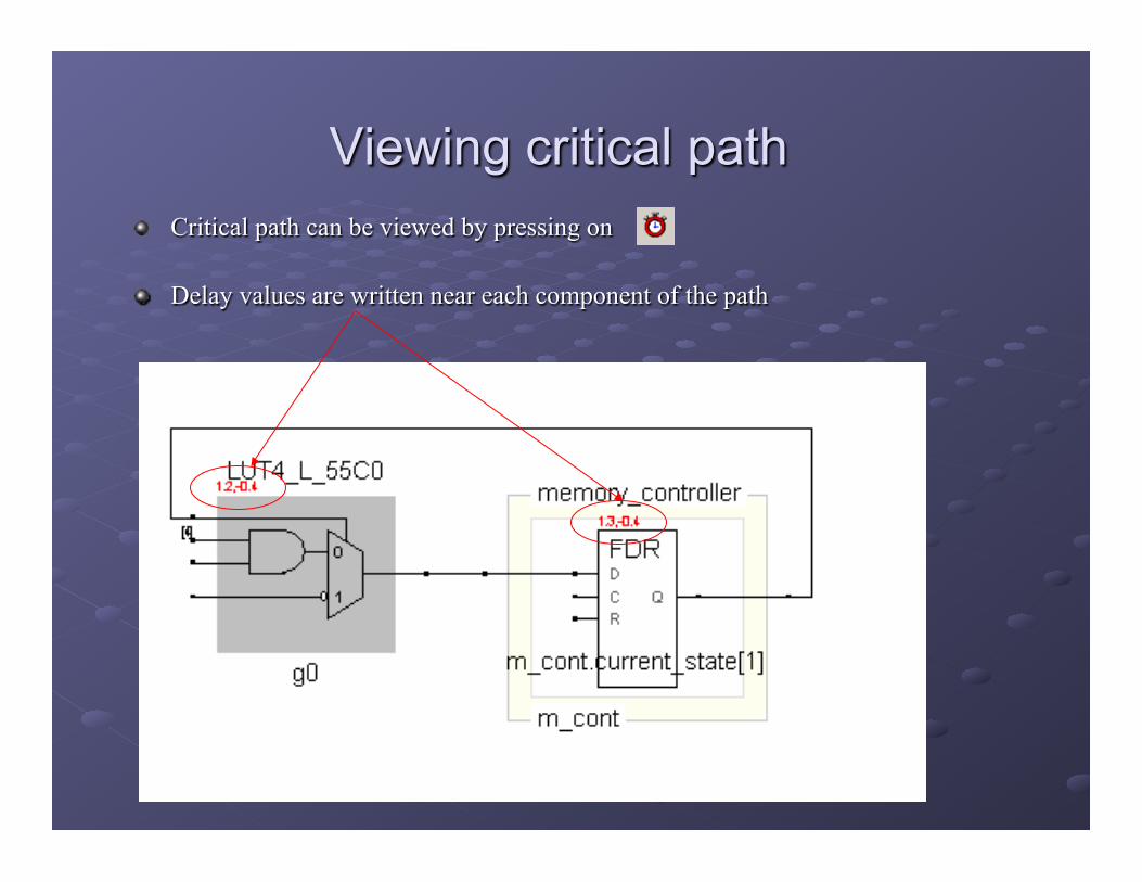
Viewing critical path " Critical path can be viewed by pressing on
" Delay values are written near each component of the path
George Mason University
Implementation
51
Implementation
• After synthesis the entire implementation process is performed by FPGA vendor tools
52
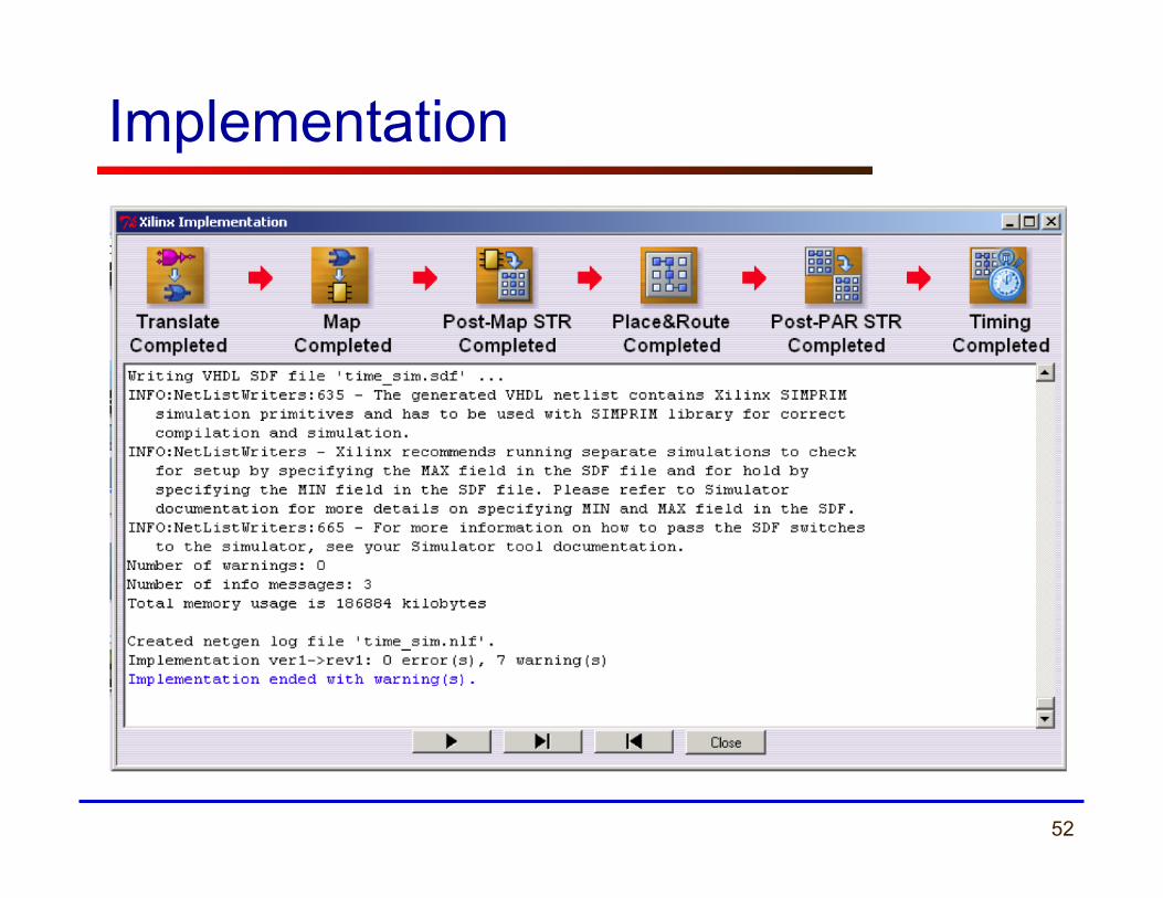
Implementation
53
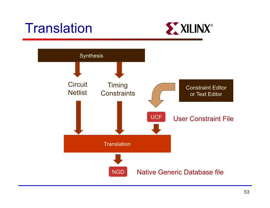
Translation
Translation
UCF
NGD Native Generic Database file
Constraint Editor or Text Editor
User Constraint File
Circuit Netlist
Timing Constraints
Synthesis

54
Mapping
LUT2
LUT3
LUT4
LUT5
LUT1 FF1
FF2
LUT0

55
Placing CLB SLICES
FPGA
56
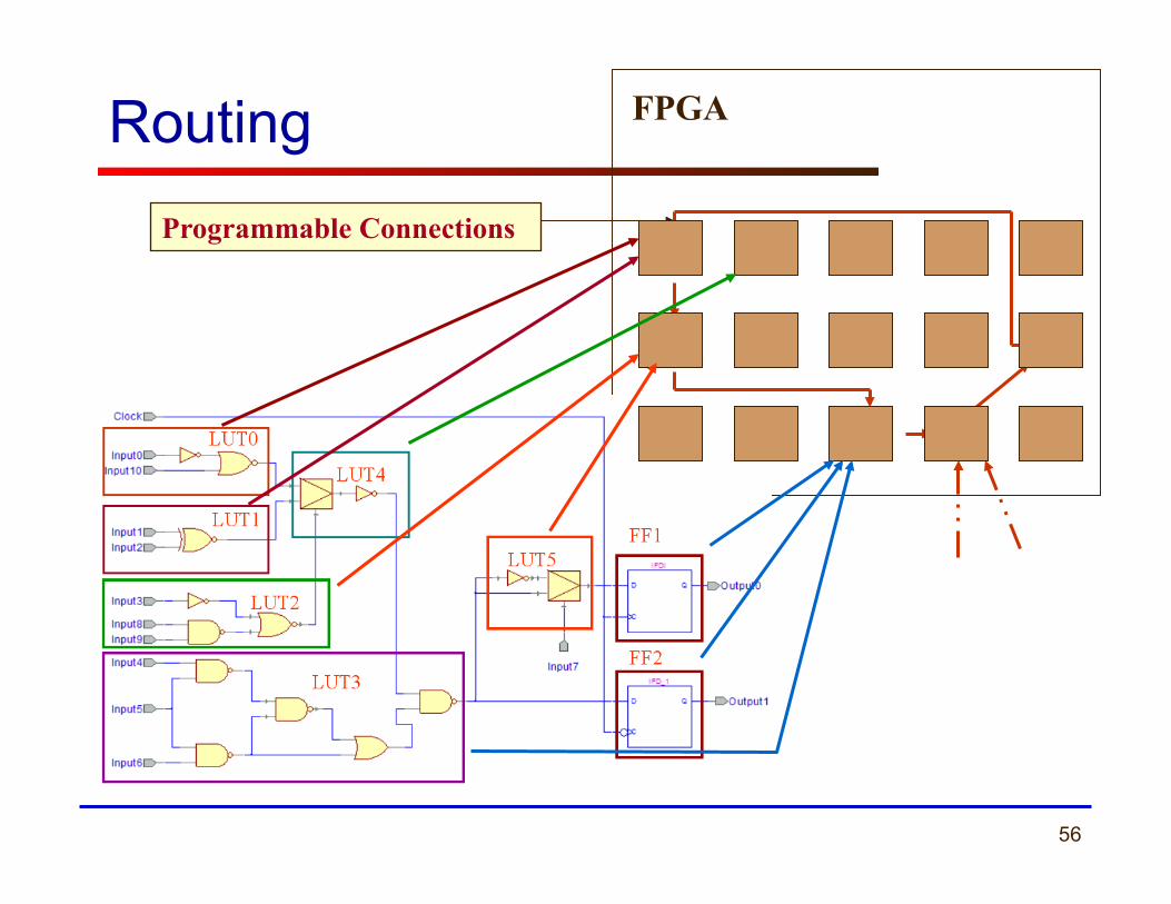
Routing Programmable Connections
FPGA
57
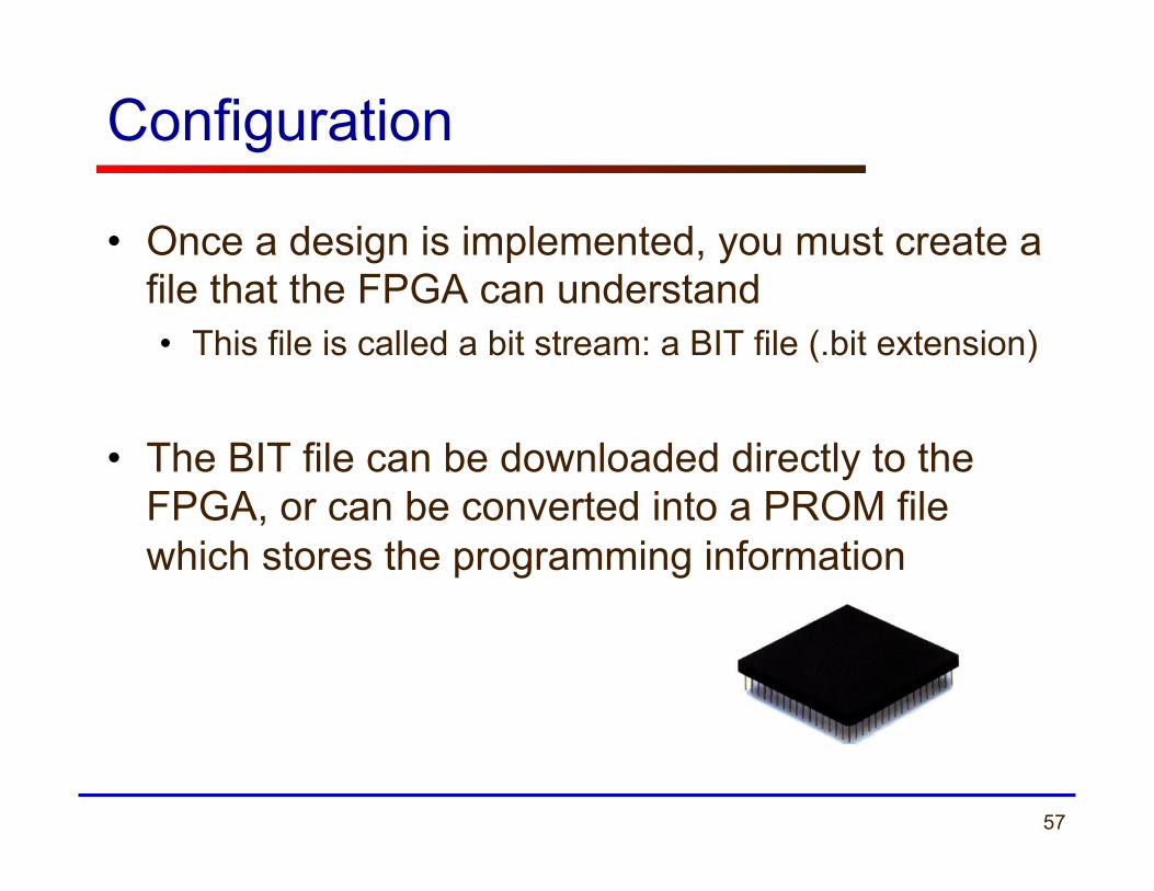
Configuration
• Once a design is implemented, you must create a file that the FPGA can understand • This file is called a bit stream: a BIT file (.bit extension)
• The BIT file can be downloaded directly to the FPGA, or can be converted into a PROM file which stores the programming information
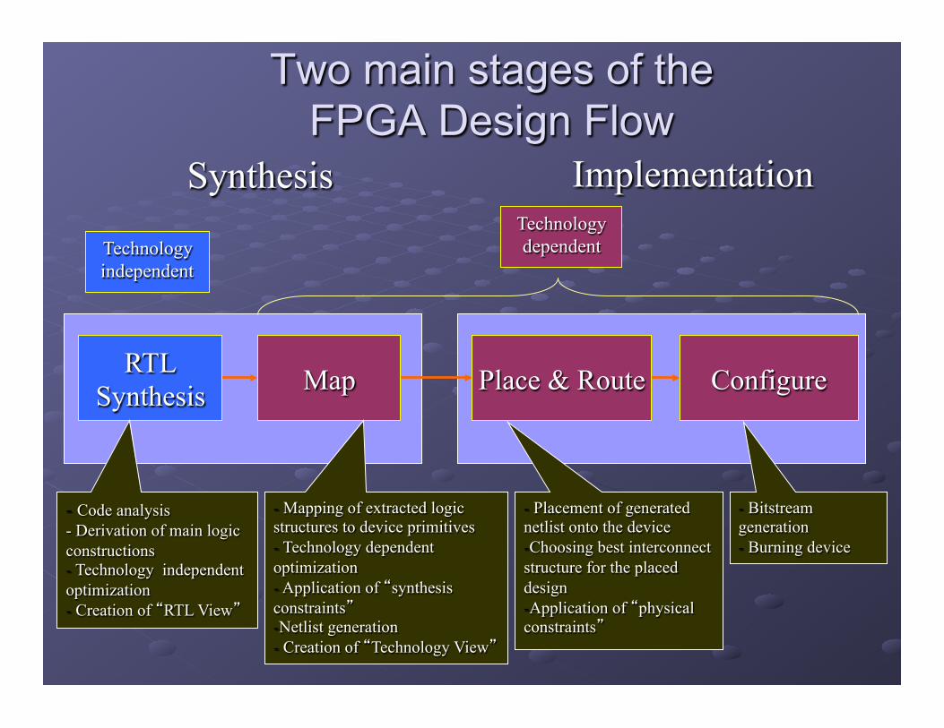
Two main stages of the FPGA Design Flow
Synthesis
Technology independent
Technology dependent
Implementation
RTL Synthesis Map Place & Route Configure
- Code analysis - Derivation of main logic constructions - Technology independent optimization - Creation of “RTL View”
- Mapping of extracted logic structures to device primitives - Technology dependent optimization - Application of “synthesis constraints” - Netlist generation - Creation of “Technology View”
- Placement of generated netlist onto the device - Choosing best interconnect structure for the placed design - Application of “physical constraints”
- Bitstream generation - Burning device