ece 4510 introduction to hardware reviewbazuinb/ece4510/review_hw.pdf · ece 4510 introduction to...
TRANSCRIPT

Material from or based on: The HCS12/9S12: An Introduction to Software & Hardware Interfacing, Thomson Delmar Learning, 2006.
ECE 4510 Introduction to Microprocessors
Hardware Review
Dr. Bradley J. BazuinAssociate Professor
Department of Electrical and Computer EngineeringCollege of Engineering and Applied Sciences
Material from or based on: The HCS12/9S12: An Introduction to Software & Hardware Interfacing, Thomson Delmar Learning, 2006.
ECE 4510/5530
2
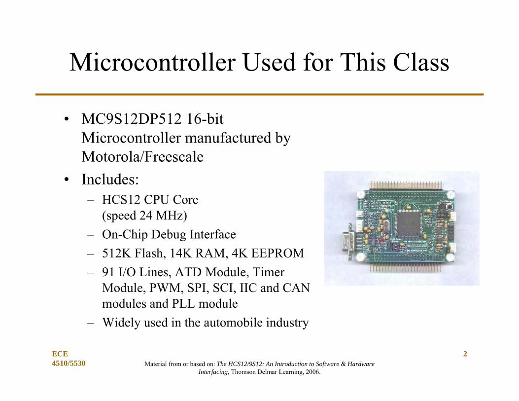
Microcontroller Used for This Class
• MC9S12DP512 16-bit Microcontroller manufactured by Motorola/Freescale
• Includes:– HCS12 CPU Core
(speed 24 MHz)– On-Chip Debug Interface– 512K Flash, 14K RAM, 4K EEPROM– 91 I/O Lines, ATD Module, Timer
Module, PWM, SPI, SCI, IIC and CAN modules and PLL module
– Widely used in the automobile industry

Material from or based on: The HCS12/9S12: An Introduction to Software & Hardware Interfacing, Thomson Delmar Learning, 2006.
Application Brochure
ECE 2510 3http://cache.freescale.com/files/microcontrollers/doc/brochure/BR1871.pdf?fpsp=1&WT_TYPE=Brochures&WT_VENDOR=FREESCALE&WT_FILE_FORMAT=pdf&WT_ASSET=Documentation
Finding This Stuff:• Freescale• 16-bit
Microcontroller• S12 and S12X• S12D

Material from or based on: The HCS12/9S12: An Introduction to Software & Hardware Interfacing, Thomson Delmar Learning, 2006.
ECE 2510
7 00 7A B
15 0D
8-bit accumulator A and Bor16-bit double accumulator D
15 0X
15 0Y
Index register X
Index register Y
15 0SP Stack pointer
15 0PC Program counter
S X H I N Z V C Condition code registerCarryOverflowZeroNegativeI Interrupt maskHalf-Carry (from bit 3)X Interrupt MaskStop Disable
Figure 1.2 HCS12 CPU registers.
HCS12 CPU Registers
• Data Registers– Two 8-bit, [A] and [B] OR– One 16-bit, [D]
• Memory index registers– Two general purpose, [X] and [Y]– One stack pointer, [SP]
• Program Counter– Instruction address, [PC]
• Condition Code Register– Bits describing completed CPU
operation or instruction results– [C] or [CCR]

Material from or based on: The HCS12/9S12: An Introduction to Software & Hardware Interfacing, Thomson Delmar Learning, 2006.
Simple Processor Diagram
• Registers Interactions
ECE 2510 5

Material from or based on: The HCS12/9S12: An Introduction to Software & Hardware Interfacing, Thomson Delmar Learning, 2006.
Important Peripherals
6ECE 4510/5530

Material from or based on: The HCS12/9S12: An Introduction to Software & Hardware Interfacing, Thomson Delmar Learning, 2006.
ECE 4510 7
DP512CPU Pins and Peripherals(No internal Busses Shown)

Material from or based on: The HCS12/9S12: An Introduction to Software & Hardware Interfacing, Thomson Delmar Learning, 2006.
ECE 4510 8
Adapt9S12DP512 I/O Pins

Material from or based on: The HCS12/9S12: An Introduction to Software & Hardware Interfacing, Thomson Delmar Learning, 2006.
Memory Map (1 of 2)
ECE 4510 9
Material from or based on: The HCS12/9S12: An Introduction to Software & Hardware Interfacing, Thomson Delmar Learning, 2006.
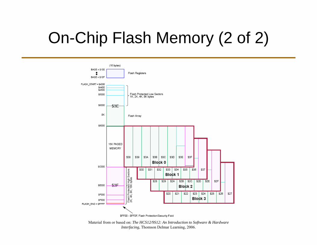
On-Chip Flash Memory (2 of 2)
Material from or based on: The HCS12/9S12: An Introduction to Software & Hardware Interfacing, Thomson Delmar Learning, 2006.
ECE 2510 11
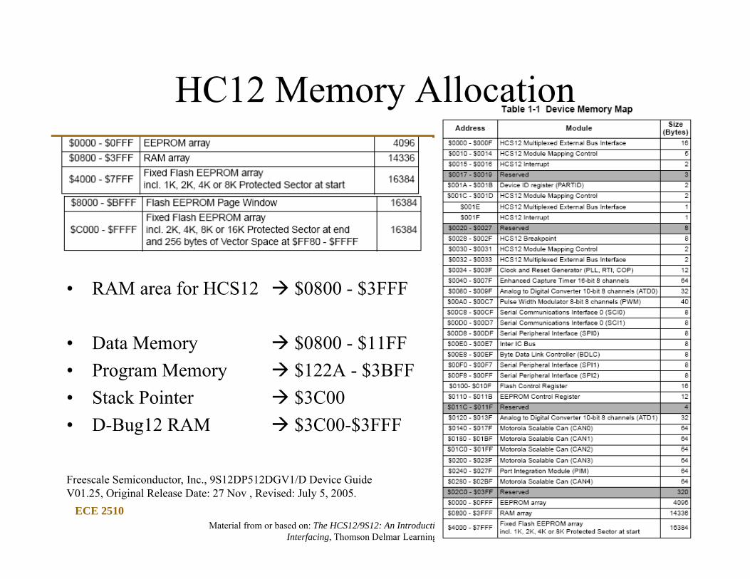
HC12 Memory Allocation
• RAM area for HCS12 $0800 - $3FFF
• Data Memory $0800 - $11FF• Program Memory $122A - $3BFF • Stack Pointer $3C00• D-Bug12 RAM $3C00-$3FFF
Freescale Semiconductor, Inc., 9S12DP512DGV1/D Device Guide V01.25, Original Release Date: 27 Nov , Revised: July 5, 2005.
Material from or based on: The HCS12/9S12: An Introduction to Software & Hardware Interfacing, Thomson Delmar Learning, 2006.
ECE 4510/5530
12
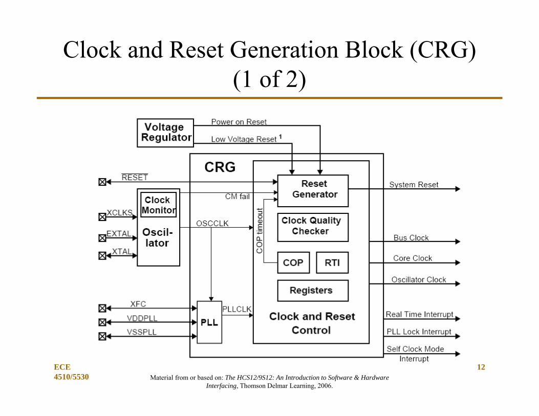
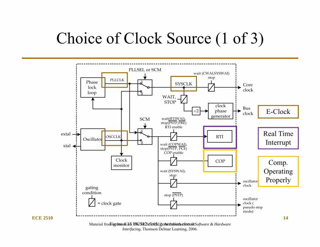
Clock and Reset Generation Block (CRG) (1 of 2)

Material from or based on: The HCS12/9S12: An Introduction to Software & Hardware Interfacing, Thomson Delmar Learning, 2006.
ECE 4510/5530
13
Clock and Reset Generation Block (CRG) (2 of 2)
• CRG generates the clock signals required by the HCS12 instruction execution and all peripheral operations.– The clock signal has the form of square waveform.
• Crystal oscillators are often used to generate clock signals.– The crystal oscillator output is sinusoidal wave and must be squared up
before it can be used. The HCS12 has an internal circuit to do this square up operation.
– The CRG block also has a PLL circuit that can multiply the frequency of the incoming clock signal.
• The CRG can also accept an external oscillator (square waveform). – The XCLKS signal must be tied low (for MC9S12DP256B) in order to
use external clock signal.
Material from or based on: The HCS12/9S12: An Introduction to Software & Hardware Interfacing, Thomson Delmar Learning, 2006.
ECE 2510 14
Phaselockloop
1
0
1
0
Clockmonitor
Oscillator OSCCLK
PLLCLK
PLLSEL or SCM
SCM
clockphase
generator2
WAIT,STOP
wait(RTIWAI),stop(PSTP,PRE)
RTI enable
RTI
COP
wait (COPWAI),stop(PSTP, PCE)
COP enable
wait (SYSWAI),stop
stop (PSTP)
wait (CWAI,SYSWAI)stop
Coreclock
Busclock
oscillatorclock
oscillatorclock (pseudo stopmode)
extal
xtal
gatingcondition
= clock gate
Figure 6.15 HCS12 clock generation circuit
SYSCLK
Choice of Clock Source (1 of 3)
E-Clock
Real Time Interrupt
Comp. Operating Properly

Material from or based on: The HCS12/9S12: An Introduction to Software & Hardware Interfacing, Thomson Delmar Learning, 2006.
ECE 4510/5530
15
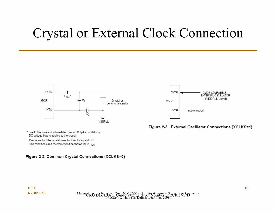
Choice of Clock Source (2 of 3)
• The user can choose between using the external crystal or oscillator to produce the clock signal.– The external crystal is connected between the EXTAL and XTAL
pins and needs an on-chip oscillator circuitry to square it up.– The external clock source provided by the oscillator is connected
to the EXTAL pin and has a 2.5V peak-to-peak magnitude for D family.
• The XCLKS signal must be grounded to select the external clock signal.
Material from or based on: The HCS12/9S12: An Introduction to Software & Hardware Interfacing, Thomson Delmar Learning, 2006.
ECE 4510/5530
16
Crystal or External Clock Connection
CRG Block User Guide V02.07, Doc. Number S12CRGV2/D

Material from or based on: The HCS12/9S12: An Introduction to Software & Hardware Interfacing, Thomson Delmar Learning, 2006.
ECE 4510/5530
17
Phase Lock Loops
• A Phase Lock Loop is capable of providing an integer change up or down in the clock rate input to the PLL– A voltage controlled oscillator is used
CRG Block User Guide V02.07, Doc. Number S12CRGV2/D

Material from or based on: The HCS12/9S12: An Introduction to Software & Hardware Interfacing, Thomson Delmar Learning, 2006.
ECE 4510/5530
18
(SYNR + 1)PLLCLK = 2 OSCCLK ----------------------- (6.1)
(REFDV + 1)
Phase Locked Loop (PLL) (1 of 5)
• The frequency of the PLLCLK is controlled by registers synthesizer (SYNR) and reference divide (REFDY) using the following equation:
NOTE: PLLCLK must not exceed the maximum operating system frequency.
Maximum bus frequency is 25 MHz.
Therefore, maximum PLLCLK is 50 MHz.
The lab modules use a 16 MHz external crystal, PLLCLK of 48 MHz, and
E-clock (bus frequency) of 24 MHz.

Material from or based on: The HCS12/9S12: An Introduction to Software & Hardware Interfacing, Thomson Delmar Learning, 2006.
ECE 4510/5530
19
RTI Counter Chain
CRG Block User Guide V02.07, Doc. Number S12CRGV2/D
102112122132142152162
161 to
Note: OSCCLK not SYSCLK and not E-Clock

Material from or based on: The HCS12/9S12: An Introduction to Software & Hardware Interfacing, Thomson Delmar Learning, 2006.
ECE 4510 20
HCS12 Parallel Ports
• The number of pins available in each I/O port for HCS12 are (see mc9s12dp512.s and mc9s12dp512.h for names):– PORTA 8 pins PA7 – PA0– PORTB 8 pins PB7 – PB0– PORTE 8 pins PE7 – PE0– PTH 8 pins PH7 – PH0– PTJ 4 pins PJ7, PJ6, PJ1, PJ0– PORTK 7 pins PK7, PK5 – PK0– PTM 8 pins PM7 – PM0– PTP 8 pins PP7 – PP0– PTS 8 pins PS7 – PS0– PTT 8 pins PT7 – PT0– PORTAD1, PORTAD0 16 pins PAD15 – PAD0

Material from or based on: The HCS12/9S12: An Introduction to Software & Hardware Interfacing, Thomson Delmar Learning, 2006.
Port Integration Module (PIM)
• Parallel Ports – the “PT#” ports: T, S, M, P, H, J
• A standard PIM port pin has the following minimum features:– Input/output selection– 5V output drive with two selectable
drive strengths– 5V digital and analog input– Input with selectable pull-up or
pull-down device• Optional features:
– Open drain for wired-or connections– Interrupt inputs with glitch filtering
ECE 4510/5530
21

Material from or based on: The HCS12/9S12: An Introduction to Software & Hardware Interfacing, Thomson Delmar Learning, 2006.
Block Diagram
ECE 4510/5530
22
• PT#: input/output data register
• PTI#: input register• DDR#: data direction
register
Material from or based on: The HCS12/9S12: An Introduction to Software & Hardware Interfacing, Thomson Delmar Learning, 2006.
ECE 4510 23
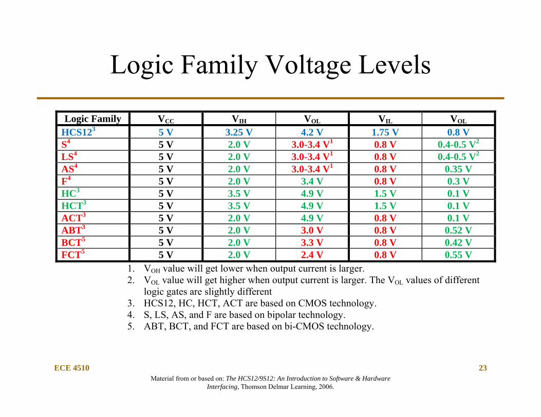
Logic Family Voltage Levels
Logic Family VCC VIH VOL VIL VOL HCS123 5 V 3.25 V 4.2 V 1.75 V 0.8 V S4 5 V 2.0 V 3.0-3.4 V1 0.8 V 0.4-0.5 V2 LS4 5 V 2.0 V 3.0-3.4 V1 0.8 V 0.4-0.5 V2 AS4 5 V 2.0 V 3.0-3.4 V1 0.8 V 0.35 V F4 5 V 2.0 V 3.4 V 0.8 V 0.3 V HC3 5 V 3.5 V 4.9 V 1.5 V 0.1 V HCT3 5 V 3.5 V 4.9 V 1.5 V 0.1 V ACT3 5 V 2.0 V 4.9 V 0.8 V 0.1 V ABT3 5 V 2.0 V 3.0 V 0.8 V 0.52 V BCT5 5 V 2.0 V 3.3 V 0.8 V 0.42 V FCT5 5 V 2.0 V 2.4 V 0.8 V 0.55 V
1. VOH value will get lower when output current is larger. 2. VOL value will get higher when output current is larger. The VOL values of different
logic gates are slightly different 3. HCS12, HC, HCT, ACT are based on CMOS technology. 4. S, LS, AS, and F are based on bipolar technology. 5. ABT, BCT, and FCT are based on bi-CMOS technology.

Material from or based on: The HCS12/9S12: An Introduction to Software & Hardware Interfacing, Thomson Delmar Learning, 2006.
ECE 4510 24
Logic Family Current Levels
Logic Family VCC IIH IIL IOH IOL HCS1223 5 V 2.5 uA 2.5 uA 25 mA 25 mA S 5 V 50 uA 1.0 mA 1 mA 20 mA LS 5 V 20 uA 0.2 mA 15 mA 24 mA AS 5 V 20 uA 0.5 mA 15 mA 64 mA F 5 V 20 uA 0.2 mA 1 mA 20 mA HC3 5 V 1 uA 1 uA 25 mA 25 mA HCT3 5 V 1 uA 1 uA 25 mA 25 mA ACT3 5 V 1 uA 1 uA 24 mA 24 mA ABT3 5 V 1 uA 1 uA 32 mA 64 mA BCT 5 V 20 uA 1 mA 15 mA 64 mA FCT3 5 V 1 uA 1 uA 15 mA 64 mA
1. Values are based on the 74XX244 devices of Texas Instruments.. 2. The total HCS supply current is 65 mA. 3. The values of IIH and IIL are input leakage currents.

Material from or based on: The HCS12/9S12: An Introduction to Software & Hardware Interfacing, Thomson Delmar Learning, 2006.
MC7805CTG Linear Regulator
5V Positive Voltage Regulator• Output Current in Excess of 1.0 A• No External Components Required• Internal Thermal Overload Protection• Internal Short Circuit Current Limiting• Output Transistor Safe−Area
Compensation• Output Voltage Offered in 1.5%, 2% and
4% Tolerance• Available in Surface Mount D2PAK−3,
DPAK−3 and Standard 3−Lead Transistor Packages
ECE 4510/5530
25
Data Sheet: MC7805CTG, ON Semiconductor

Material from or based on: The HCS12/9S12: An Introduction to Software & Hardware Interfacing, Thomson Delmar Learning, 2006.
ECE 4510 26
Interfacing with LEDs
• Three methods for interfacing with LED’s• Method A and B are recommended for use with LED’s that
need only 1 to 2mA to produce enough brightness• The circuit C is required for use with LED’s that need
larger current to light and the ECE 4510/5530 labs• Circuit C Resistor value can be between 330 ohm and 1
Kohm
74HC04
VCC
Figure 7.29 An LED connected to a CMOS inverter through a current- limiting resistor.
Portpin
(a) positive direct drive (c) buffered drive
R1
R2
R3
VCC
Portpin
Portpin(b) inverse direct
drive

Material from or based on: The HCS12/9S12: An Introduction to Software & Hardware Interfacing, Thomson Delmar Learning, 2006.
ECE 4510 27
Lab LED and Light Bar Connections
• Buffer the HC12 port– Inverting buffer ‘540– Non-inverting buffer ‘541– Provide current sinking for the
LED
• Resistor between +5 and LED– If you short the LED while
probing, the resistor provides current limiting
• Resistor Value– LED needs ~1.2 to 1.8 V drop– LED wants ~ 10 mA
38010
2.15mA
VVR
32010
8.15mA
VVR

Material from or based on: The HCS12/9S12: An Introduction to Software & Hardware Interfacing, Thomson Delmar Learning, 2006.
ECE 4510 28
Connecting DIP SwitchesVCC
10K
PA0PA1PA2PA3PA4PA5PA6PA7
HCS12
Figure 7.39 Connecting a set of eight DIP switches to Port A of the HCS12
SW DIP-8

Material from or based on: The HCS12/9S12: An Introduction to Software & Hardware Interfacing, Thomson Delmar Learning, 2006.
ECE 4510 29
Buffering Dip Switches
• For the ECE 4510 Lab, all dip switches should be buffered.
• One possible buffering configuration is shown here

Material from or based on: The HCS12/9S12: An Introduction to Software & Hardware Interfacing, Thomson Delmar Learning, 2006.
Electro-Mechanical Relay
ECE 4510/5530
30

Material from or based on: The HCS12/9S12: An Introduction to Software & Hardware Interfacing, Thomson Delmar Learning, 2006.
Lab 4 Relay Design
ECE 4510/5530
31

Material from or based on: The HCS12/9S12: An Introduction to Software & Hardware Interfacing, Thomson Delmar Learning, 2006.
Driving an LED Array
Lighting One LED• Source current to a row• Selectively sink current
from a column
Matrix Driving• Separately source all rows
where LEDs are to turn on in Column 1 AND sink current from only column 1.
• Do the next column … and repeat.ECE
4510/553032Lite-On Technology Corp. LTP-757G
20 mA, 2.1-2.6V80 mA, 3.0-3.7V

Material from or based on: The HCS12/9S12: An Introduction to Software & Hardware Interfacing, Thomson Delmar Learning, 2006.
5x7 Matrix with Source and Sink ICs
ECE 4510 33
MIC5891 SourceLTP-757G or similar DisplayULN2803A Sink[note shown 74HCT595 shift reg.]
(Future Sink: TPIC6C596N)

Material from or based on: The HCS12/9S12: An Introduction to Software & Hardware Interfacing, Thomson Delmar Learning, 2006.
Light Patterns
• Storage for each pattern– A: 0x1F, 0x24, 0x44, 0x24, 0x1F– B: 0x7F, 0x49, 0x49, 0x49, 0x36
ECE 4510/5530
34

Material from or based on: The HCS12/9S12: An Introduction to Software & Hardware Interfacing, Thomson Delmar Learning, 2006.
ECE 4510 35
Keypad Circuitry
A
B
C
D
E
F
0
1
2
3
4
5
6
7
8
9
10K
VC C
PA7
PA6
PA5
PA4
PA3
PA2
PA1
PA0
HCS12 MCU
Figure 7 .41 S ixteen-key keypad connected to the H C S12
PA7 PA6 PA5 PA4 Selected keys
1110
1101
1011
0111
0,4,8,C,
1,5,9,D,
2,6,A,E,
and 3and 7and Band F
Table 7.16 Sixteen-key keypad row selections
outputs
inputs

Material from or based on: The HCS12/9S12: An Introduction to Software & Hardware Interfacing, Thomson Delmar Learning, 2006.
ECE 4510 36
Keypad Operation
• PortA pins PA3 – PA0 are pulled up to high by pull-up resistors
• Whenever a key switch is pressed, the corresponding row and column are shorted together
• In order to distinguish the row being scanned and those not being scanned, the row being scanned is driven low, where as other rows are driven high
PA7 PA6 PA5 PA4 Selected keys
1110
1101
1011
0111
0,4,8,C,
1,5,9,D,
2,6,A,E,
and 3and 7and Band F
Table 7.16 Sixteen-key keypad row selections

Material from or based on: The HCS12/9S12: An Introduction to Software & Hardware Interfacing, Thomson Delmar Learning, 2006.
Class Keypads
ECE 4510/5530
37
Material from or based on: The HCS12/9S12: An Introduction to Software & Hardware Interfacing, Thomson Delmar Learning, 2006.
ECE 4510 38
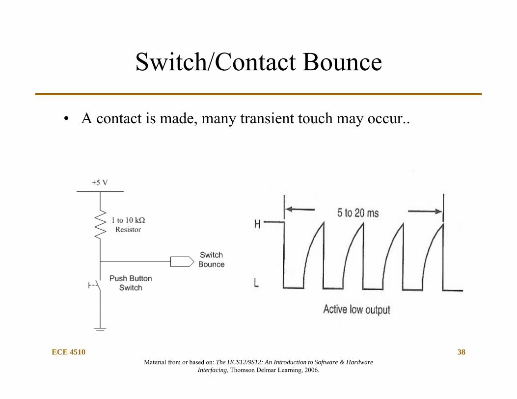
Switch/Contact Bounce
• A contact is made, many transient touch may occur..
Material from or based on: The HCS12/9S12: An Introduction to Software & Hardware Interfacing, Thomson Delmar Learning, 2006.
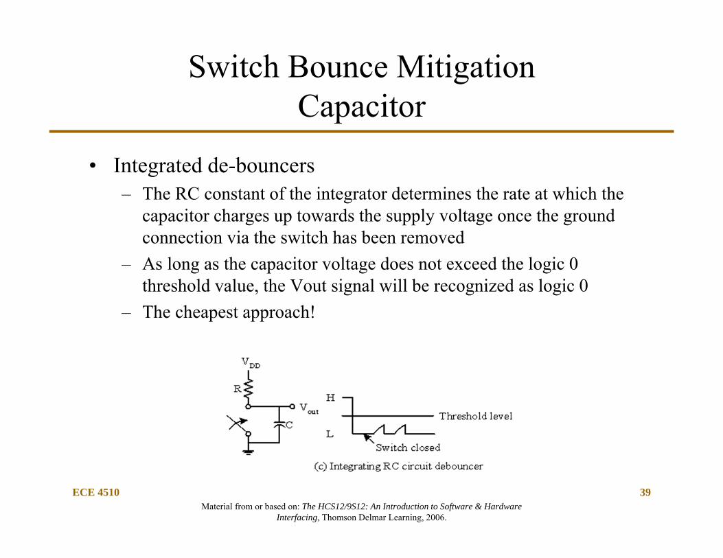
ECE 4510 39
Switch Bounce MitigationCapacitor
• Integrated de-bouncers– The RC constant of the integrator determines the rate at which the
capacitor charges up towards the supply voltage once the ground connection via the switch has been removed
– As long as the capacitor voltage does not exceed the logic 0 threshold value, the Vout signal will be recognized as logic 0
– The cheapest approach!
Material from or based on: The HCS12/9S12: An Introduction to Software & Hardware Interfacing, Thomson Delmar Learning, 2006.
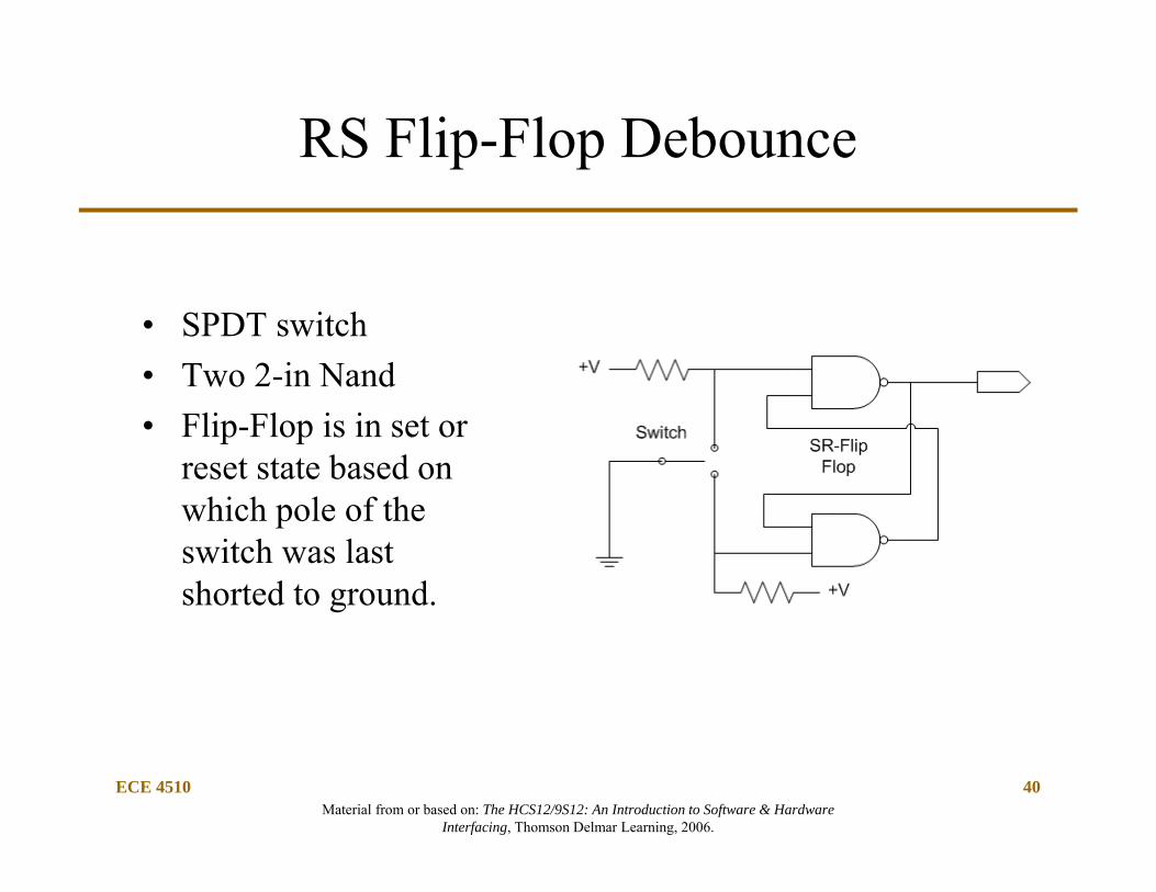
RS Flip-Flop Debounce
• SPDT switch• Two 2-in Nand• Flip-Flop is in set or
reset state based on which pole of the switch was last shorted to ground.
ECE 4510 40
Material from or based on: The HCS12/9S12: An Introduction to Software & Hardware Interfacing, Thomson Delmar Learning, 2006.
ECE 4510 41
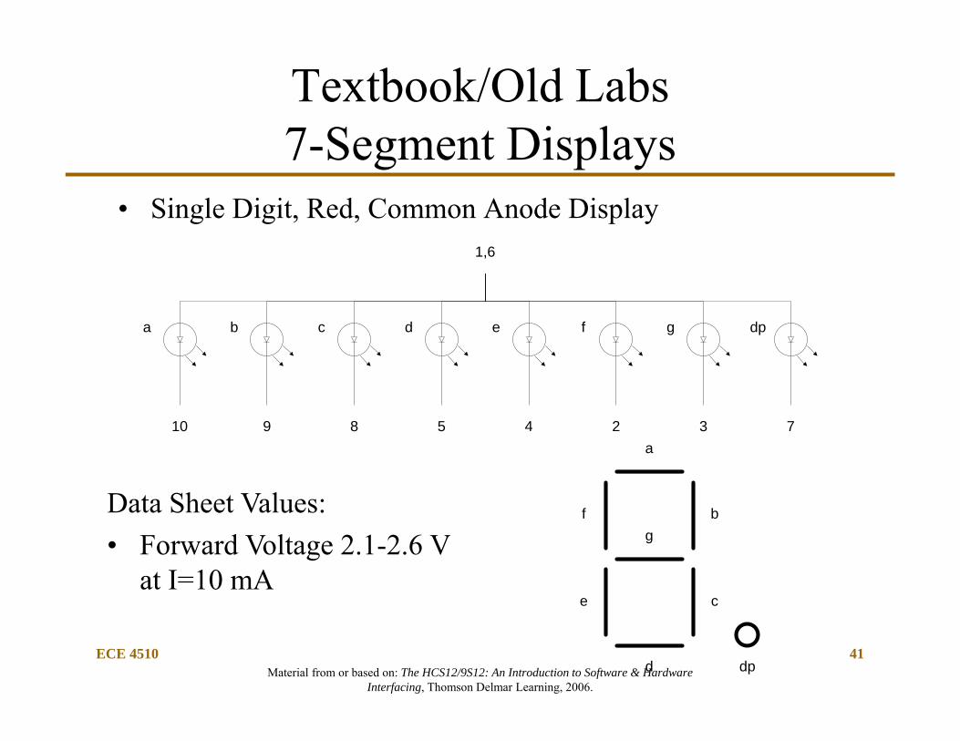
Textbook/Old Labs7-Segment Displays
• Single Digit, Red, Common Anode Display
a b c d e f g dp
1,6
10 9 8 5 4 2 3 7a
b
c
d
e
fg
dp
Data Sheet Values:• Forward Voltage 2.1-2.6 V
at I=10 mA

Material from or based on: The HCS12/9S12: An Introduction to Software & Hardware Interfacing, Thomson Delmar Learning, 2006.
ECE 4510 42
Driving a Common Anode Display
• Forward Voltage 2.1-2.6 Vat I=10 mA a b c d e f g dp
1,6
1 2 3 4 5 6 7 8
916 15 14 13 12 11 10
HC12 Pin
HC12 Pin
HC12 Pin
HC12 Pin
HC12 Pin
HC12 Pin
HC12 Pin
HC12 Pin
‘540 Inverting
Buffer
10 9 8 5 4 2 3 7
mA
VtoVVR10
6.21.25
290240 R
Material from or based on: The HCS12/9S12: An Introduction to Software & Hardware Interfacing, Thomson Delmar Learning, 2006.
ECE 4510 43
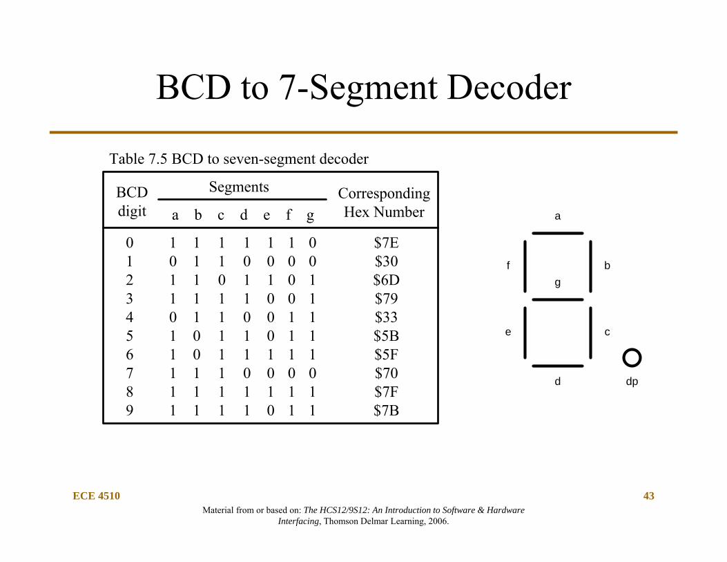
BCD to 7-Segment Decoder
BCDdigit a b c d e f g
Segments Corresponding Hex Number
0123456789
1011011111
1111100111
1101111111
1011011011
1010001010
1000111011
0011111011
$7E$30$6D$79$33$5B$5F$70$7F$7B
Table 7.5 BCD to seven-segment decoder
a
b
c
d
e
fg
dp

Material from or based on: The HCS12/9S12: An Introduction to Software & Hardware Interfacing, Thomson Delmar Learning, 2006.
ECE 4510 44
Multiple Displays, Common Cathode
• Some applications needs to display multiple BCD digits, then time multiplexing technique will be used
• Seven segment displays consists of either a common anode or common cathode which plays a key role in turning on and off the seven segment display
• Common Cathode (Note: The lab used common Anode)– Common cathode of the seven segment display is connected to the
collector of an NPN transistor– When a high voltage is applied to the base of the NPN transistor, it is
driven to saturation – The common cathode of the display will then be driven low allowing the
display to be lighted– By turning the NPN transistors ON and OFF many times in a second,
multiple digits can be displayed

Material from or based on: The HCS12/9S12: An Introduction to Software & Hardware Interfacing, Thomson Delmar Learning, 2006.
ECE 4510 45
Multiple 7-Segment Displays, Common Cathode
.
.
.
ab
g
PB6 PB5 PB0
Figure 7.32 P ort B and P ort K together drive six seven-segment displays (M C9S12DP 256)
. . .. . .
. . .74HC244
HCS12
ab
g
.
.
.
c o m m o nc athode
c o m m o ncathode
c o m m o nc athode
ab
g
I MA
X = 7
0 m
A
.
.
.
R
R
R 2N2222
2N2222
2N2222
300
PK5
PK4
PK0
300
#5 #4 #0

Material from or based on: The HCS12/9S12: An Introduction to Software & Hardware Interfacing, Thomson Delmar Learning, 2006.
The HCS12 Timer Elements
ECE 4510/5530
46
Prescaler
16-bit counter
Input CaptureOutput compare
Channel 0
Input CaptureOutput compare
Channel 1
Input CaptureOutput compare
Channel 2
Input CaptureOutput compare
Channel 3
Input CaptureOutput compare
Channel 4
Input CaptureOutput compare
Channel 5
Input CaptureOutput compare
Channel 6
Input CaptureOutput compare
Channel 7
Registers
16-bit Pulseaccumulator A
IOC0
IOC1
IOC2
IOC3
IOC4
IOC5
IOC6
IOC7
Bus clock
Timer overflowinterrupt
TC0 interrupt
TC1 interrupt
TC2 interrupt
TC3 interrupt
TC4 interrupt
TC5 interrupt
TC6 interrupt
TC7 interrupt
PA overflowinterruptPA inputinterrupt
Figure 8.1 HCS12 Standard Timer (TIM) block diagram
• 16-bit free-running main timer
– Prescalaer• 16-bit modulus
downcounter– Prescalaer– Load
• Control Registers• Interrupt Registers• Capture/Compare Registers

Material from or based on: The HCS12/9S12: An Introduction to Software & Hardware Interfacing, Thomson Delmar Learning, 2006.
ECE 4510/5530
47
T Pin Related Registers
• Timer Counter Registers– TIOS = $40– TCFORC = $41– TOC7M = $42– TOC7D = $43
– TCNT = $44 (16-bit)– TSCR1 = $46– TTOV = $47– TCTL1 = $48– TCTL2 = $49– TCTL3 = $4A– TCTL4 = $4B– TIE = $4C– TSCR2 = $4D– TFLG1 = $4E– TFLG2 = $4F
• Timer Counter Registers– TC0 = $50 (16-bit)– TC1 = $52 (16-bit)– TC2 = $54 (16-bit)– TC3 = $56 (16-bit)– TC4 = $58 (16-bit)– TC5 = $5A (16-bit)– TC6 = $5C (16-bit)– TC7 = $5E (16-bit)
– and more …

Material from or based on: The HCS12/9S12: An Introduction to Software & Hardware Interfacing, Thomson Delmar Learning, 2006.
Timer Block Diagram (Latch Mode)
ECE 4510/5530
48
Prescaler 16-bit free-runningmain timer
pin logic Delaycounter
comparator
TCx capture/compareregister
TCxH hold register
EDG x
Prescalerbus clock÷1, 4, 8, 16
÷1,2,...,128 16-bit load register
16-bit modulusdown counter
ICLAT, LATQ, BUFEN(force latch)
write $0000 tomodulus counter
LATQ(MDC latch enable)
Latc
hFigure 8.35 Enhanced Input capture function block diagram in latch mode
to other IC channels
bus clock
PTxone IC channel
(IC0..IC3)
pin logicPTicomparator
TCx capture/compareregisterMUX
EDG i
EDG jj = 8 - i
one IC channel(IC4..IC7)

Material from or based on: The HCS12/9S12: An Introduction to Software & Hardware Interfacing, Thomson Delmar Learning, 2006.
Timer Block Diagram (Queue Mode)
ECE 4510/5530
49
Prescaler 16-bit free-runningmain timer
pin logic Delaycounter
comparator
TCx capture/compareregister
TCxH hold register
EDG x
Prescalerbus clock÷1, 4, 8, 16
÷1,2,...,128 16-bit load register
16-bit modulusdown counter
Figure 8.36 Enhanced Input capture function block diagram in Queue mode (channels IC0..IC3 block diagram)
to other IC channels
bus clock
PTxone IC channel
(IC0..IC3)
pin logicPTicomparator
TCx capture/compareregisterMUX
EDG i
EDG jj = 8 - i
one IC channel(IC4..IC7)

Material from or based on: The HCS12/9S12: An Introduction to Software & Hardware Interfacing, Thomson Delmar Learning, 2006.
ECE 4510/5530
50
HCS12DP256
PT5
3.3 F
Buzzer
Figure 8.21 Circuit connection for a buzzer
Chapter 8 Example Making Sound
• A sound can be generated by creating a digital waveform with appropriate frequency and using it to drive a speaker or a buzzer.
• The simplest song is a two-tone siren.

Material from or based on: The HCS12/9S12: An Introduction to Software & Hardware Interfacing, Thomson Delmar Learning, 2006.
LM386
• Input gain control using potentiometer
• Device Gain control 20-200 with feedback RC
• Drives an 8 ohm speaker
ECE 4510/5530
51
$0.93 ea. at Digikey

Material from or based on: The HCS12/9S12: An Introduction to Software & Hardware Interfacing, Thomson Delmar Learning, 2006.
Speaker
ECE 4510/5530
52
$1.10 ea. at Digikey

Material from or based on: The HCS12/9S12: An Introduction to Software & Hardware Interfacing, Thomson Delmar Learning, 2006.
Distance Measurement UsingTime-of-Flight (TOF)
• Distances are measured based on the round-trip ultrasonic signals time-of-flight.
ECE 4510/5530
53
TofCDist air 2
2TofCDist air
PING)))™ Ultrasonic Distance Sensor (#28015), Parallax Inc., v1.5 2/15/2008, see www.parallax.com.
Material from or based on: The HCS12/9S12: An Introduction to Software & Hardware Interfacing, Thomson Delmar Learning, 2006.
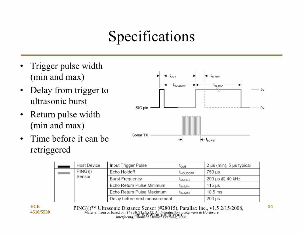
Specifications
• Trigger pulse width (min and max)
• Delay from trigger to ultrasonic burst
• Return pulse width (min and max)
• Time before it can be retriggered
ECE 4510/5530
54PING)))™ Ultrasonic Distance Sensor (#28015), Parallax Inc., v1.5 2/15/2008, see www.parallax.com.

Material from or based on: The HCS12/9S12: An Introduction to Software & Hardware Interfacing, Thomson Delmar Learning, 2006.
Bi-Directional Bus
• Output to bus under the control of an enable signal• Input from bus whenever a read is desired• Bus at known high or low level when not “driven”
ECE 4510/5530
55
Busses are typically pulled-up

Material from or based on: The HCS12/9S12: An Introduction to Software & Hardware Interfacing, Thomson Delmar Learning, 2006.
ECE 4510/5530
56
Channel 7
Period and duty Counter
PWM Channels
Channel 6
Period and duty Counter
Channel 5
Period and duty Counter
Channel 4
Period and duty Counter
Channel 3
Period and duty Counter
Channel 2
Period and duty Counter
Channel 1
Period and duty Counter
Channel 0
Period and duty Counter
Clock select
Control
PWMclock
PWM Module
Enable
Polarity
Alignment
Bus clock
PWM7
PWM6
PWM5
PWM4
PWM3
PWM2
PWM1
PWM0
Figure 8.38 HCS12 PWM block diagram
PWM Block Diagram

Material from or based on: The HCS12/9S12: An Introduction to Software & Hardware Interfacing, Thomson Delmar Learning, 2006.
Making Clocks
ECE 4510/5530
57
A ClockSA ClockChannels 0, 1, 4, 5
B ClockSB ClockChannels 2, 3, 6, 7

Material from or based on: The HCS12/9S12: An Introduction to Software & Hardware Interfacing, Thomson Delmar Learning, 2006.
ECE 4510/5530
58
GATE8-bit counter
PWMCNTx
8-bit compare=
PWMDTYx
clocksource
8-bit compare=
PWMPERx
T Q
QR
MUX
T
R
CAExQ
Q
MUX
to pindriver
PPOLx
From port PTPdata register(clock edge sync)
PWMEx
up/down re
set
Figure 8.44 PWM channel block diagram
PWM Channel Block Diagram
Material from or based on: The HCS12/9S12: An Introduction to Software & Hardware Interfacing, Thomson Delmar Learning, 2006.
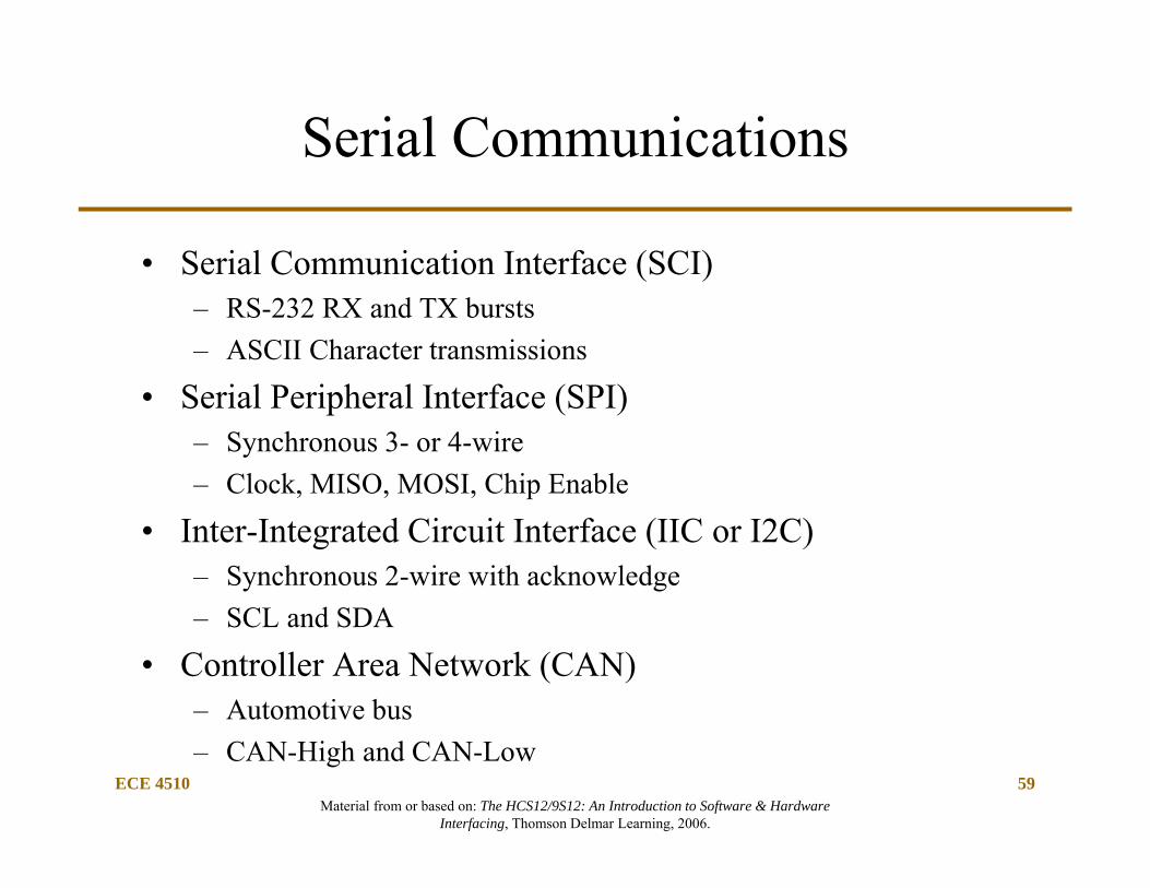
Serial Communications
• Serial Communication Interface (SCI)– RS-232 RX and TX bursts – ASCII Character transmissions
• Serial Peripheral Interface (SPI)– Synchronous 3- or 4-wire – Clock, MISO, MOSI, Chip Enable
• Inter-Integrated Circuit Interface (IIC or I2C)– Synchronous 2-wire with acknowledge– SCL and SDA
• Controller Area Network (CAN)– Automotive bus– CAN-High and CAN-Low
ECE 4510 59

Material from or based on: The HCS12/9S12: An Introduction to Software & Hardware Interfacing, Thomson Delmar Learning, 2006.
ECE 4510/5530
Data Format for Asynchronous Data Communication
• Data is transmitted character by character bit-serially.• A character consists of
– one start bit (0)– 7 to 8 data bits (often, an ASCII character plus a parity bit)– an optional parity bit– one, or one and a half, or two stop bits (1)– least significant bit is transmitted first– most significant bit is transmitted last
Note: Transceivers invert the signal to the appropriate logical and voltage levels of the physical layer.

Material from or based on: The HCS12/9S12: An Introduction to Software & Hardware Interfacing, Thomson Delmar Learning, 2006.
ECE 4510/5530
61
TxDRxDCD
CTS
DSRGND
RTS
TxDRxDCDCTS
DSRGND
RTS
Computer(DTE)
Modem(DCE)
TxDRxDCD
CTS
DSRGND
RTS
TxDRxDCDCTS
DSRGND
RTS
Direct link
Computer(DTE)
Modem(DCE)
Figure 9.2 Point-to-point asynchronous connection
EIA-232-E Procedural Specification (2 of 2)
Null modem cable: Computer to Computer
Material from or based on: The HCS12/9S12: An Introduction to Software & Hardware Interfacing, Thomson Delmar Learning, 2006.
ECE 4510/5530
62
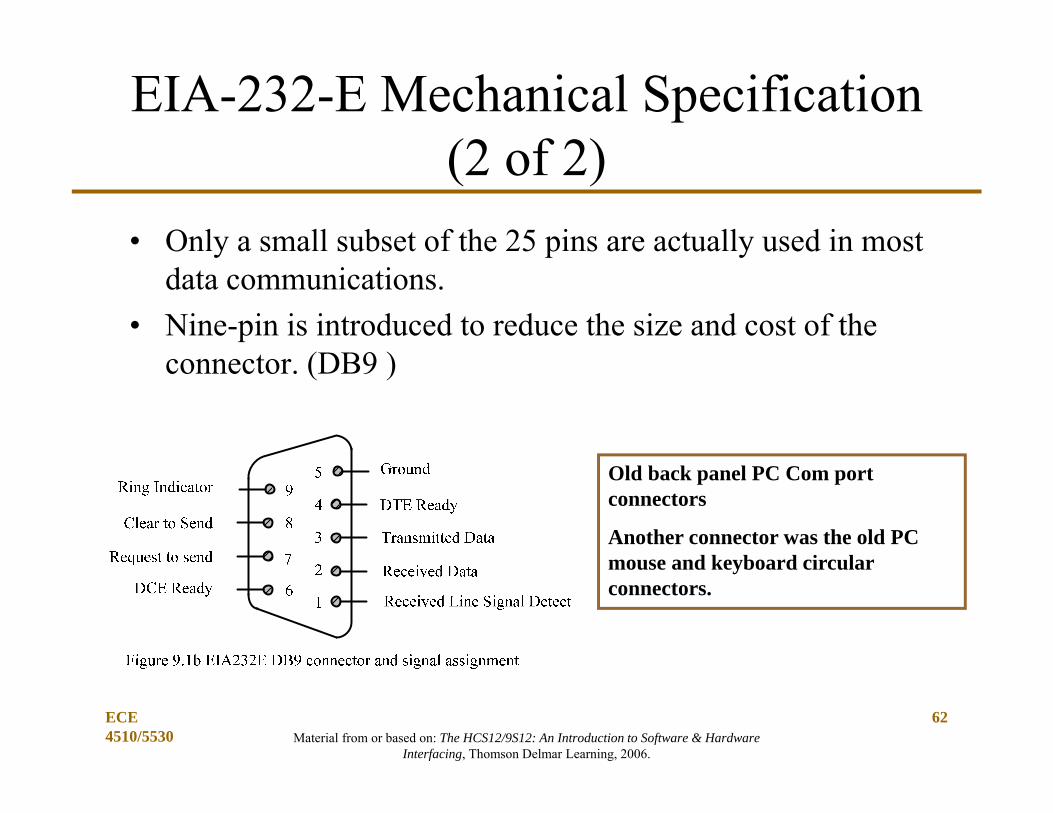
EIA-232-E Mechanical Specification (2 of 2)
• Only a small subset of the 25 pins are actually used in most data communications.
• Nine-pin is introduced to reduce the size and cost of the connector. (DB9 )
Old back panel PC Com port connectors
Another connector was the old PC mouse and keyboard circular connectors.

Material from or based on: The HCS12/9S12: An Introduction to Software & Hardware Interfacing, Thomson Delmar Learning, 2006.
ECE 4510/5530
DB9 Signals
• A point-to-point linkAlways has to be present• Signal ground (GND) – (Voltage reference for other pins)• Transmitted data (Tx) – (output from uP, serial data transmission)• Received data (Rx) – (input to uP, serial data received)Hardware Handshaking (sometimes present)• Request to send (RTS) – (output from uP, connect to CTS if not used)• Clear to send (CTS) – (input to uP, connect to RTS if not used)
State of the DTEs and what the “line” is doing (not often used anymore)• Data set ready (DSR) – (input to uP, set high if not used)• DTE Ready (DTR) – (output from uP, pair with DSR, set high if not used)• Carrier detect (CD) – (input to uP, the phone/modem is ringing)• Ring Indicator (RI) – (input to uP, the phone is ringing , not required)
Material from or based on: The HCS12/9S12: An Introduction to Software & Hardware Interfacing, Thomson Delmar Learning, 2006.
ECE 4510/5530
64
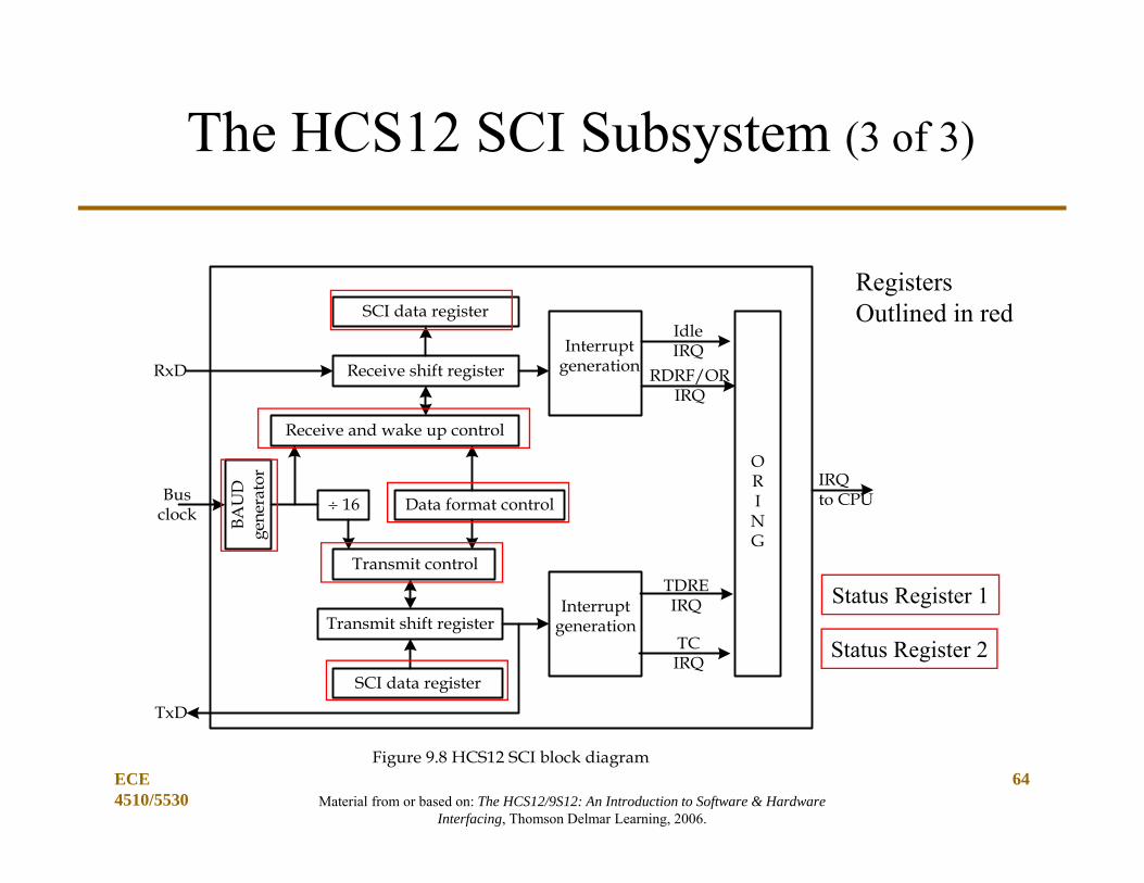
SCI data register
Receive shift register
Receive and wake up control
BAU
Dge
nera
tor
16 Data format control
Transmit control
Transmit shift register
SCI data register
Busclock
RxDInterrupt
generation
Interruptgeneration
IdleIRQ
RDRF/ORIRQ
TDREIRQ
TCIRQ
ORI
NG
IRQto CPU
TxD
Figure 9.8 HCS12 SCI block diagram
Status Register 1
Status Register 2
The HCS12 SCI Subsystem (3 of 3)
Registers Outlined in red

Material from or based on: The HCS12/9S12: An Introduction to Software & Hardware Interfacing, Thomson Delmar Learning, 2006.
ECE 4510/5530
65
BAUD dividerBusclock
SBR12-SBR0
16 SCI Data Register
H 8 7 6 5 3 2 1 0 L
STO
P
STA
RT
M
T8
Paritygeneration
PEPT
Transmitter control
load
from
SC
IDR
Shift
ena
ble
prea
mbl
e (a
ll on
es)
Brea
ks (a
ll 0s
)TE SBKTDRE
TIE
TCTCIE
TDRE interrupt request
TC interrupt request
LoopControl
LoopsRSRC
To RxD
TxD
Figure 9.12 SCI transmitter block diagram
Internal Bus
MSB
4
Transmitter Block Diagram

Material from or based on: The HCS12/9S12: An Introduction to Software & Hardware Interfacing, Thomson Delmar Learning, 2006.
Receiver Block Diagram
ECE 4510/5530
66
BAUD dividerBusclock
SBR12-SBR0 SCI Data Register
H 8 7 6 5 3 2 1 0 L
STO
P
STA
RT
PEPT
IDLEILIE
RIE
IDLE interrupt request
RDRF/OR interrupt request
Figure 9.15 SCI receiver block diagram
Internal Bus
11-bit receive shift register
4
FENFPE
RWUWakeup
logic
Paritychecking
R8
RDRFOR
All
ones
MSB
WAKEILT
M
RERAF
Datarecovery
RxD
Loopcontrol
FromTxD
LOOPSRSRC

Material from or based on: The HCS12/9S12: An Introduction to Software & Hardware Interfacing, Thomson Delmar Learning, 2006.
Parts Kit RS-232 Transceiver ICMAX232IN• Meets or Exceeds TIA/EIA-232-F
and ITU• Recommendation V.28• Operates From a Single 5-V Power
Supply With 1.0-uF Charge-Pump Capacitors
• Operates Up To 120 kbit/s• Two Drivers and Two Receivers• ±30-V Input Levels• Low Supply Current . . . 8 mA
Typical• ESD Protection Exceeds JESD 22
– 2000-V Human-Body Model (A114-A)
• Upgrade With Improved ESD (15-kV HBM) and 0.1-uF Charge-Pump Capacitors is
• Available With the MAX202• Applications
– TIA/EIA-232-F, Battery-Powered Systems,– Terminals, Modems, and Computers
ECE 4510/5530
67
Material from or based on: The HCS12/9S12: An Introduction to Software & Hardware Interfacing, Thomson Delmar Learning, 2006.
ECE 4510/5530
PS1/TxD
PS0/RxD
Note: Both CTS and RTS arejumpered to an I/O pin in casehardware handshake is needed
CTS*
RTS*
T1IN
T2IN
R1OUT
R2OUT
T1OUT
T2OUT
R1IN
R2IN
11
10
12
9
8
13
7
14
1
6
2
7
3
8
4
9
5
DCD
DSR
RxD
RTS
TxD
CTS
DTR
RI
GND
DB9 connector
DS14C232
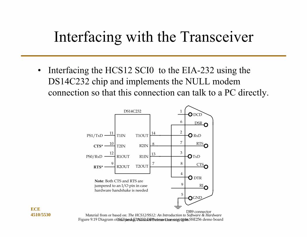
Figure 9.19 Diagram of SCI and EIA232 DB9 connector wiring in SSE256 demo board
Interfacing with the Transceiver
• Interfacing the HCS12 SCI0 to the EIA-232 using the DS14C232 chip and implements the NULL modem connection so that this connection can talk to a PC directly.

Material from or based on: The HCS12/9S12: An Introduction to Software & Hardware Interfacing, Thomson Delmar Learning, 2006.
RS-232 Transceivers
• Sunseeeker board-to-board connection– RTS/CTS hardware signaling connected– A null modem cable used for board to board communications.– Intersil ICL3222CB – 18 pin SOIC
ECE 4510/5530
69
Material from or based on: The HCS12/9S12: An Introduction to Software & Hardware Interfacing, Thomson Delmar Learning, 2006.
ECE 4510 70
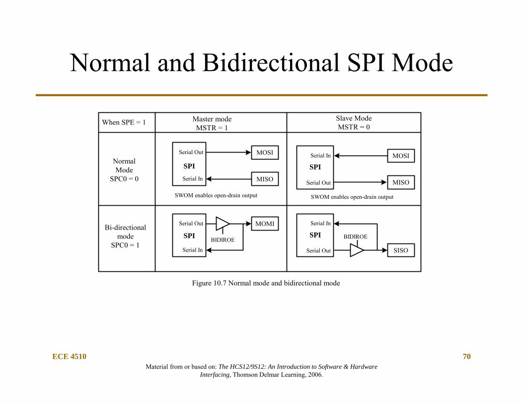
Figure 10.7 Normal mode and bidirectional mode
Serial Out
SPI
Serial In
MOSI
MISO
When SPE = 1
NormalMode
SPC0 = 0
Master modeMSTR = 1
Serial Out
SPI
Serial In
MOMI
BIDIROE
Serial Out
SPI
Serial In
SISO
BIDIROE
Serial Out
SPISerial In MOSI
MISO
Slave ModeMSTR = 0
SWOM enables open-drain output SWOM enables open-drain output
Bi-directionalmode
SPC0 = 1
Normal and Bidirectional SPI Mode
Material from or based on: The HCS12/9S12: An Introduction to Software & Hardware Interfacing, Thomson Delmar Learning, 2006.
SPI Data Transfer Example
ECE 2510 71
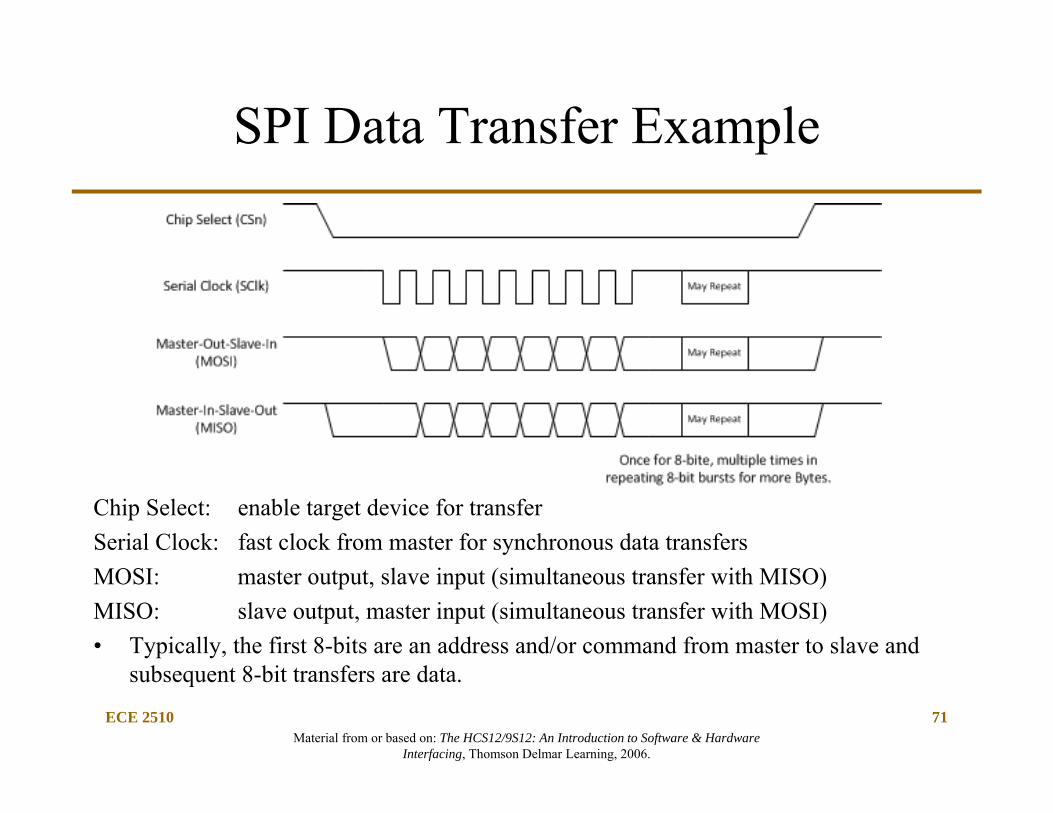
Chip Select: enable target device for transferSerial Clock: fast clock from master for synchronous data transfersMOSI: master output, slave input (simultaneous transfer with MISO)MISO: slave output, master input (simultaneous transfer with MOSI)• Typically, the first 8-bits are an address and/or command from master to slave and
subsequent 8-bit transfers are data.

Material from or based on: The HCS12/9S12: An Introduction to Software & Hardware Interfacing, Thomson Delmar Learning, 2006.
ECE 4510 72
Shift register
Shift register
Baud RateGenerator
VDD
MISO
MOSI
SCK SCK
MOSI
MISO
SSSS
Master SPI Slave SPI
Figure 10.8 Master/slave transfer block diagram
Single IC Interconnection
Material from or based on: The HCS12/9S12: An Introduction to Software & Hardware Interfacing, Thomson Delmar Learning, 2006.
ECE 4510 73
SS
+5V
MOSI SCK MISO SS
Shiftregister
MOSI SCK MISO SS
Shiftregister
MOSI SCK MISO
Shiftregister
SS
SPI Master(HCS12)
SCKx
MOSIx
MISOx
PP0
PP1
PPk
.
.
.
.
.
.
. . .
Slave 0 Slave 1 Slave k
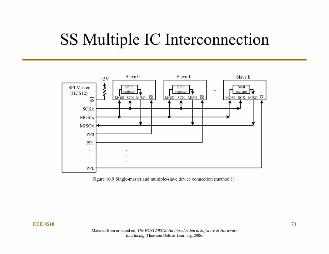
Figure 10.9 Single-master and multiple-slave device connection (method 1)
SS Multiple IC Interconnection

Material from or based on: The HCS12/9S12: An Introduction to Software & Hardware Interfacing, Thomson Delmar Learning, 2006.
ECE 4510 74
Daisy Chained Multiple IC Interconnection
SS
+5VMOSI SCK MISO SS
Shiftregister
MOSI SCK MISO SS
Shiftregister
MOSI SCK MISO
Shiftregister
SS
SPI Master(HCS12)
SCKx
MOSIx
MISOx
. . .
Slave 0 Slave 1 Slave k
Figure 10.10 Single-master and multiple-slave device connection (method 2)
. . .

Material from or based on: The HCS12/9S12: An Introduction to Software & Hardware Interfacing, Thomson Delmar Learning, 2006.
ECE 4510 75
SS (O)master only
SS (I)
SCK (CPOL = 0)
SCK (CPOL = 1)Sample I
MOSI/MISO
Change OMOSI Pin
Change OMISO Pin
tT tI tLMinimum 1/2 SCK
for tT, tI, tL
tL
MSB first (LSBF = 0)LSB first (LSBF = 1)
MSBLSB
Bit 6Bit 1
Bit 5Bit 2
Bit 4Bit 3
Bit 3Bit 4
Bit 2Bit 5
Bit 1Bit 6
LSBMSB
Begin EndTransfer
Figure 10.5 SPI Clock format 0 (CPHA = 0)
SPI Transmission Format (2 of 3)

Material from or based on: The HCS12/9S12: An Introduction to Software & Hardware Interfacing, Thomson Delmar Learning, 2006.
ECE 4510 76
SS (O)master only
SS (I)
SCK (CPOL = 0)
SCK (CPOL = 1)Sample I
MOSI/MISO
Change OMOSI Pin
Change OMISO Pin
tT tI tLMinimum 1/2SCK for tT, tI, tL
tLMSB first (LSBF = 0)LSB first (LSBF = 1)
MSBLSB
Bit 6Bit 1
Bit 5Bit 2
Bit 4Bit 3
Bit 3Bit 4
Bit 2Bit 5
Bit 1Bit 6
LSBMSB
Begin EndTransfer
Figure 10.6 SPI Clock format 1 (CPHA = 1)
SPI Transmission Format (3 of 3)

Material from or based on: The HCS12/9S12: An Introduction to Software & Hardware Interfacing, Thomson Delmar Learning, 2006.
Motorola/FreescaleDOCUMENT NUMBER S12SPIV3/D
ECE 4510/5530
77
Material from or based on: The HCS12/9S12: An Introduction to Software & Hardware Interfacing, Thomson Delmar Learning, 2006.
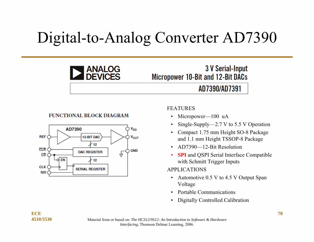
Digital-to-Analog Converter AD7390
FEATURES• Micropower—100 uA• Single-Supply—2.7 V to 5.5 V Operation• Compact 1.75 mm Height SO-8 Package
and 1.1 mm Height TSSOP-8 Package• AD7390—12-Bit Resolution• SPI and QSPI Serial Interface Compatible
with Schmitt Trigger InputsAPPLICATIONS
• Automotive 0.5 V to 4.5 V Output Span Voltage
• Portable Communications• Digitally Controlled Calibration
ECE 4510/5530
78

Material from or based on: The HCS12/9S12: An Introduction to Software & Hardware Interfacing, Thomson Delmar Learning, 2006.
AD7390 DAC
• Note: LDn appears to be is backwards?! High SPI Shift/Low Update ADC Out
ECE 4510/5530
79
Material from or based on: The HCS12/9S12: An Introduction to Software & Hardware Interfacing, Thomson Delmar Learning, 2006.
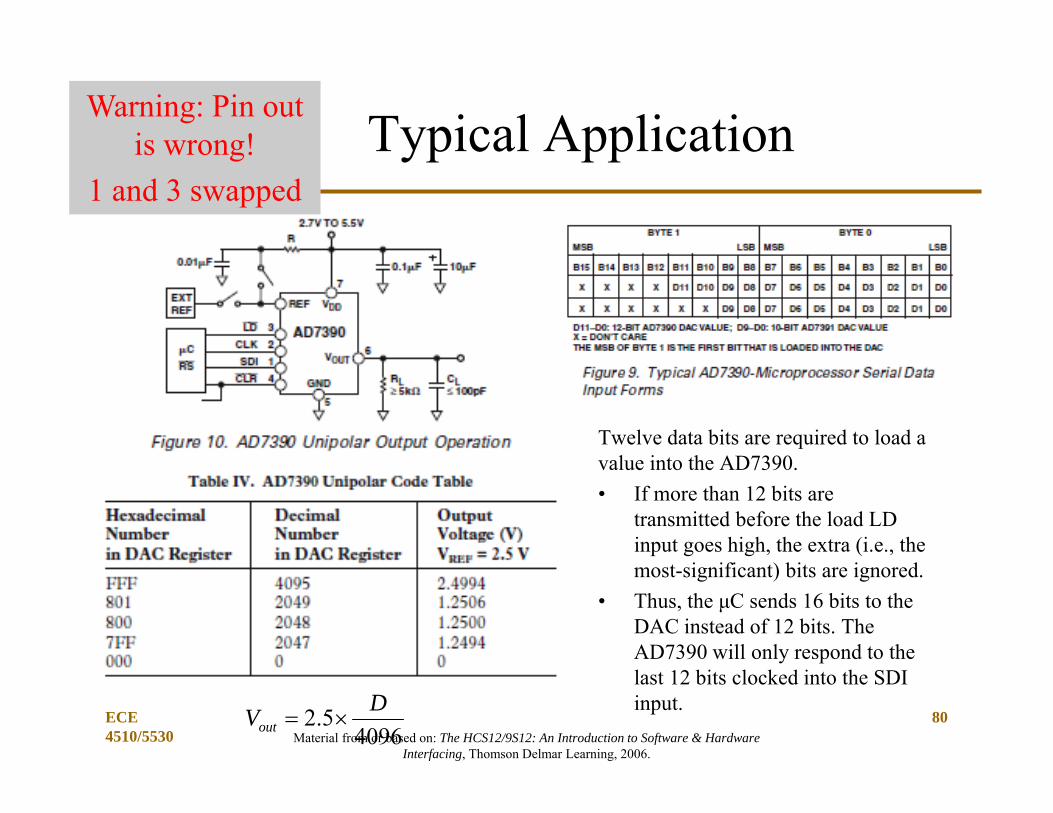
Typical Application
Twelve data bits are required to load a value into the AD7390. • If more than 12 bits are
transmitted before the load LD input goes high, the extra (i.e., the most-significant) bits are ignored.
• Thus, the μC sends 16 bits to the DAC instead of 12 bits. The AD7390 will only respond to the last 12 bits clocked into the SDI input.
ECE 4510/5530
804096
5.2 DVout
Warning: Pin out is wrong!
1 and 3 swapped

Material from or based on: The HCS12/9S12: An Introduction to Software & Hardware Interfacing, Thomson Delmar Learning, 2006.
The AD7705
FEATURES• AD7705: 2 fully differential input channel ADCs– 16 bits no missing codes– 0.003% nonlinearity
• Programmable gain front end: gains from 1 to 128• 3-wire serial interface– SPI®-, QSPI™-, MICROWIRE™-, and
DSP-compatible Schmitt-trigger input on SCLK
• Ability to buffer the analog input• 2.7 V to 3.3 V or 4.75 V to 5.25 V operation• Power dissipation 1 mW maximum @ 3 V• Standby current 8 μA maximum• 16-lead PDIP, 16-lead SOIC, and 16-lead TSSOP packages
ECE 4510/5530
81

Material from or based on: The HCS12/9S12: An Introduction to Software & Hardware Interfacing, Thomson Delmar Learning, 2006.
AD7705 Application
Lab 8 Configuration– 5 V Supply (bypass Caps)– 2.5 V reference TLE2425– 4-wire SPI (include CSn)– AIN1+ and AIN1-
differential input– External Clock – 1 MHz
(PWM or ECT)400kHz to 2.5 MHz
– DRDYn Data Ready Poll/Interrupt Line
ECE 4510/5530
82
CSn
CLK

Material from or based on: The HCS12/9S12: An Introduction to Software & Hardware Interfacing, Thomson Delmar Learning, 2006.
Temperature Sensor LM35
• Precision Centigrade Temperature Sensor– It has three pins with voltage output directly proportional to the
ambient temperature.
• It can measure temperature in the range of +2ºC to 150ºC with a supply from 4~205V.
• Voltage output at 0 mV + 10 mV/ºC

Material from or based on: The HCS12/9S12: An Introduction to Software & Hardware Interfacing, Thomson Delmar Learning, 2006.
Three Terminal Device
CAPACITIVE LOADS• Like most micropower circuits, the LM35 has a limited ability to drive heavy capacitive
loads. The LM35 by itself is able to drive 50 pf without special precautions. If heavier loads are anticipated, it is easy to isolate or decouple the load with a resistor; see Figure 3. Or you can improve the tolerance of capacitance with a series R-C damper from output to ground; see Figure 4.
ECE 4510/5530
84From Texas Instruments data sheet SNIS159B

Material from or based on: The HCS12/9S12: An Introduction to Software & Hardware Interfacing, Thomson Delmar Learning, 2006.
Inter-Integrated Circuit (IIC) Interface
Wired-OR ConfigurationExternal pull-ups

Material from or based on: The HCS12/9S12: An Introduction to Software & Hardware Interfacing, Thomson Delmar Learning, 2006.
Byte Level Transfer
• Every byte put on the SDA line must be eight bits long. The number of bytes that can be transmitted per transfer is unrestricted. Each byte must be followed by an Acknowledge bit. Data is transferred with the Most Significant Bit (MSB) first (see Figure 6). If a slave cannot receive or transmit another complete byte of data until it has performed some other function, it can hold the clock line SCL LOW to force the master into a wait state. Data transfer then continues when the slave is ready for another byte of data and releases clock line SCL.
NXP, I2C-bus specification and user manual, Rev. 5 — 9 October 2012http://www.nxp.com/documents/user_manual/UM10204.pdf
ECE 4510/5530
86

Material from or based on: The HCS12/9S12: An Introduction to Software & Hardware Interfacing, Thomson Delmar Learning, 2006.
Data Transfer Format (7-bit addressing)
• Master transmitter to slave receiver – shown in Figure 11.10.

Material from or based on: The HCS12/9S12: An Introduction to Software & Hardware Interfacing, Thomson Delmar Learning, 2006.
Data Transfer Format (7-bit addressing)
• Master reads slave immediately after the first byte (address byte) – shown in Figure 11.11.

Material from or based on: The HCS12/9S12: An Introduction to Software & Hardware Interfacing, Thomson Delmar Learning, 2006.
IIC Block Diagram
Registers

Material from or based on: The HCS12/9S12: An Introduction to Software & Hardware Interfacing, Thomson Delmar Learning, 2006.
I2C Real-Time Clock/Calendar MCP7940M
Features• Real-Time Clock/Calendar (RTCC):
– Hours, Minutes, Seconds, Day of Week, Day, Month and Year
– Dual alarm with single output
• On-Chip Digital Trimming/Calibration:– Range -127 to +127 ppm, Resolution 1 ppm
• Programmable Open-Drain Output Control:– CLKOUT with 4 selectable frequencies– Alarm output
• 64 Bytes SRAM• Low-Power CMOS Technology:
– Dynamic Current: 400 �A max write
• 100 kHz and 400 kHz Compatibility• ESD Protection >4,000V• Packages include 8-Lead SOIC, TSSOP,
2x3 TDFN, MSOP and PDIP• Temperature Ranges:
– Industrial (I): -40°C to +85°C

Material from or based on: The HCS12/9S12: An Introduction to Software & Hardware Interfacing, Thomson Delmar Learning, 2006.
Typical Application Schematic

Material from or based on: The HCS12/9S12: An Introduction to Software & Hardware Interfacing, Thomson Delmar Learning, 2006.
CAN Physical Layer
• Data Frames are transmitted on a two-wire common bus as CAN high (CAN_H) and CAN low (CAN_L) signals.
ECE 4510 92

Material from or based on: The HCS12/9S12: An Introduction to Software & Hardware Interfacing, Thomson Delmar Learning, 2006.
Physical Layer Signal Levels
• Both bus lines are at a nominal 2.5V– CAN_H goes from recessive (“1”) to dominant (“0”) by going
high to nominally 3.5 V– CAN_L goes from recessive (“1”) to dominant (“0”) by going low
to nominally 1.5 V
ECE 4510 93
CAN_H
CAN_L
2.5V
DominantRecessive Recessive
1.5V
3.5V
0V
5V
Figure 13.42 Nominal CAN bus levels
voltage

Material from or based on: The HCS12/9S12: An Introduction to Software & Hardware Interfacing, Thomson Delmar Learning, 2006.
Start offrame
Arbitrationfield
Controlfield
Datafield
CRCfield
ACKfield
End offrame
Data FrameInterframe
space
Interframespace oroverload
frame
Figure 13.2 CAN Data frame
CAN Signaling Frame
• A data frame consists of seven fields: start-of-frame, arbitration, control, data, CRC, ACK, and end-of-frame.

Material from or based on: The HCS12/9S12: An Introduction to Software & Hardware Interfacing, Thomson Delmar Learning, 2006.
Multiple CAN Frames
ECE 4510/5530
95

Material from or based on: The HCS12/9S12: An Introduction to Software & Hardware Interfacing, Thomson Delmar Learning, 2006.
ACK Field
• Consists of two bits• The first bit is the acknowledgement bit.
– This bit is set to recessive by the transmitter, but will be reset to dominant if a receiver acknowledges the data frame.
• The second bit is the ACK delimiter and is recessive.
The ACK must be transmitted by another device on the CAN bus!• If no ACK received, the message will be
retransmitted … indefinitely.• So, you never run CAN without at least two fully
operational devices on the bus!

Material from or based on: The HCS12/9S12: An Introduction to Software & Hardware Interfacing, Thomson Delmar Learning, 2006.
Nominal bit time
sync_seg prop_seg phase_seg1 phase_seg2
Sample point
Figure 13.12 Nominal bit time
Nominal Bit Time
• The inverse of the nominal bit rate is the nominal bit time.• A nominal bit time is divided into four segments as shown
in Figure 13.12.

Material from or based on: The HCS12/9S12: An Introduction to Software & Hardware Interfacing, Thomson Delmar Learning, 2006.
MUXOscillator clock
Bus clockPrescaler
CANCLK
Controland
Status
Configurationregisters
Receive/TransmitEngine
Messagefiltering
andbuffering
Low passfilter
Tx int. req.
Rx int. req.
Err. int. req.
Wake-up int. req.
RxCAN
TxCAN
Figure 13.13 MSCAN12 block diagram
Tq clk
wake-up
HCS12 MSCAN Peripheral

Material from or based on: The HCS12/9S12: An Introduction to Software & Hardware Interfacing, Thomson Delmar Learning, 2006.
Overview of the HCS12 CAN Module (1 of 2)
• An HCS12 device may have from one to five on-chip CAN modules.
• Each CAN module has five receive buffers with FIFO storage scheme and three transmit buffers.
• Each of the three transmit buffers may be assigned with a local priority.
• Maskable identifier filter supports two full size extended identifier filters (32-bit), four 16-bit filters, or eight 8-bit filters.
– Only receive frames within a range of predefined identifiers (don’t have to deal with all the traffic)
• The CAN module has a programmable loopback mode that supports self-test operation.
• The CAN module has a listen-only mode for monitoring of the CAN bus.

Material from or based on: The HCS12/9S12: An Introduction to Software & Hardware Interfacing, Thomson Delmar Learning, 2006.
address register name
$_x0$_x1$_x2$_x3$_x4$_x5$_x6$_x7$_x8$_x9$_xA$_xB$_xC$_xD$_xE$_xF
Identifier register 0Identifier register 1Identifier register 2Identifier register 3
Data segment register 0Data segment register 1Data segment register 2Data segment register 3Data segment register 4Data segment register 5Data segment register 6Data segment register 7
Data length registerTransmit buffer priority register1
Time stamp register high byte2
Time stamp register low byte2
Note 1. Not applicable for receive buffer. 2. Read only for CPU
Figure 13.33 MSCAN message buffer organization
MSCAN Message Buffers
• The receive message and transmit message buffers have the same outline.

Material from or based on: The HCS12/9S12: An Introduction to Software & Hardware Interfacing, Thomson Delmar Learning, 2006.
ID28 ID27 ID26 ID25 ID24 ID23 ID22 ID21
ID20 ID19 ID18 SRR(=1)IDE(=1) ID17 ID16 ID15
ID14 ID13 ID12 ID11 ID10 ID9 ID8 ID7
ID6 ID5 ID4 ID3 ID2 ID1 ID0 RTR
7 6 5 4 3 2 1 0
Figure 13.34 Receive/transmit message buffer extended identifier
IDR0
IDR1
IDR2
IDR3
ID10 ID9 ID8 ID7 ID6 ID5 ID4 ID3
ID2 ID1 ID0 RTR IDE(=0)
7 6 5 4 3 2 1 0
Figure 13.35 Receive/transmit message buffer standard identifier
IDR0
IDR1
IDR2
IDR3
Identifier Registers (IDR0~IDR3)
• All four identifier registers are compared when a message with extended identifier is received.
• Only the first two identifier registers are compared when a message with standard identifier is received.

Material from or based on: The HCS12/9S12: An Introduction to Software & Hardware Interfacing, Thomson Delmar Learning, 2006.
16-bit Identifier Acceptance(MASK and ID Values)
ECE 4510 102
• CANxIDMR0-7 provide masking of whether an identifier bit is tested or not
• CANxIDAR0-7 provides the value to compare for unmasked bits
Material from or based on: The HCS12/9S12: An Introduction to Software & Hardware Interfacing, Thomson Delmar Learning, 2006.
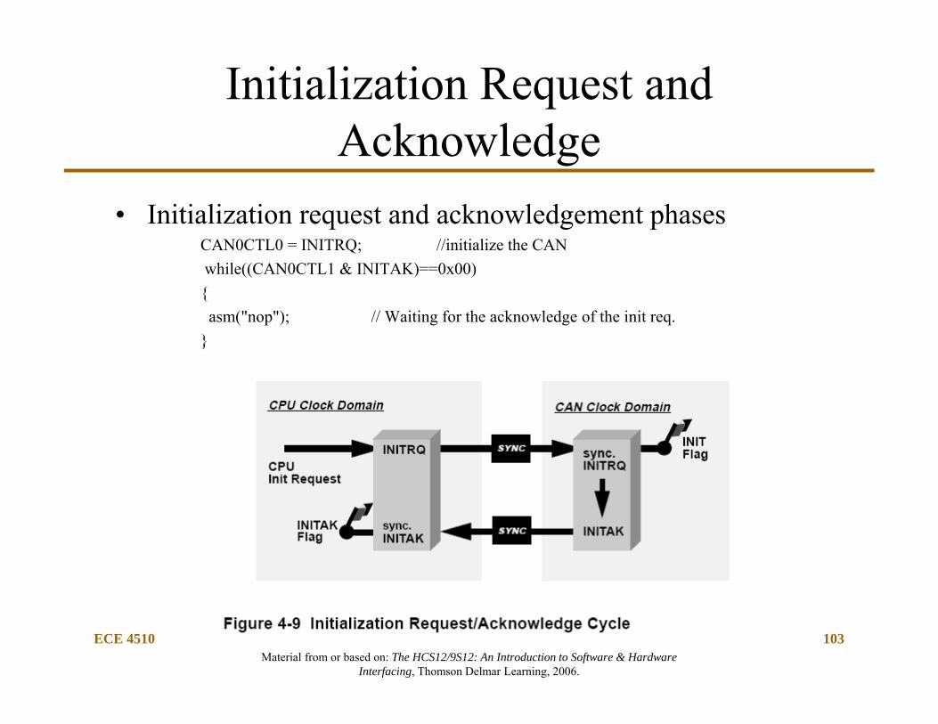
Initialization Request and Acknowledge
• Initialization request and acknowledgement phasesCAN0CTL0 = INITRQ; //initialize the CANwhile((CAN0CTL1 & INITAK)==0x00){
asm("nop"); // Waiting for the acknowledge of the init req.}
ECE 4510 103

Material from or based on: The HCS12/9S12: An Introduction to Software & Hardware Interfacing, Thomson Delmar Learning, 2006.
Interfacing the CAN to the HCS12
Material from or based on: The HCS12/9S12: An Introduction to Software & Hardware Interfacing, Thomson Delmar Learning, 2006.
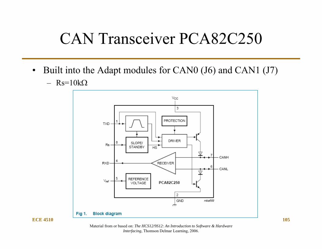
CAN Transceiver PCA82C250
ECE 4510 105
• Built into the Adapt modules for CAN0 (J6) and CAN1 (J7)– Rs=10k

Material from or based on: The HCS12/9S12: An Introduction to Software & Hardware Interfacing, Thomson Delmar Learning, 2006.
TI CAN Transceiver
• 3.3V Transceivers shown.– Note: CANH voltage limited
to Vcc
• 5.0V Transceivers are available SN65HVD251and SN65HVD255-7
ECE 4510/5530
106
Material from or based on: The HCS12/9S12: An Introduction to Software & Hardware Interfacing, Thomson Delmar Learning, 2006.
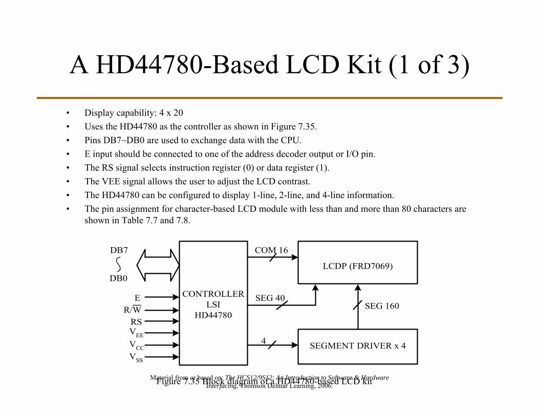
DB7
DB0
ER/W
RSVEE
VCCVSS
COM 16
LCDP (FRD7069)
SEG 160SEG 40
4 SEGMENT DRIVER x 4
CONTROLLERLSI
HD44780
Figure 7.35 Block diagram of a HD44780-based LCD kit
A HD44780-Based LCD Kit (1 of 3)• Display capability: 4 x 20• Uses the HD44780 as the controller as shown in Figure 7.35.• Pins DB7~DB0 are used to exchange data with the CPU.• E input should be connected to one of the address decoder output or I/O pin.• The RS signal selects instruction register (0) or data register (1).• The VEE signal allows the user to adjust the LCD contrast.• The HD44780 can be configured to display 1-line, 2-line, and 4-line information.• The pin assignment for character-based LCD module with less than and more than 80 characters are
shown in Table 7.7 and 7.8.
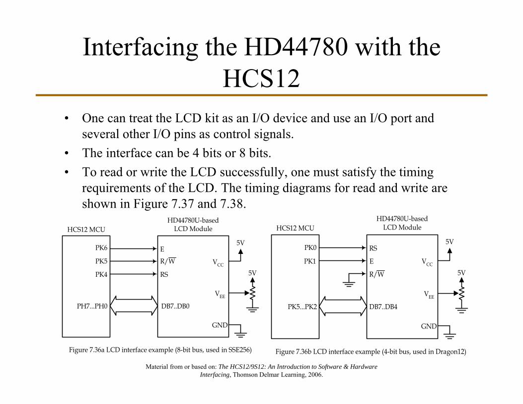
Material from or based on: The HCS12/9S12: An Introduction to Software & Hardware Interfacing, Thomson Delmar Learning, 2006.
PK4
PK6
PK5
PH7...PH0 DB7..DB0
E
RS
R/W
HD44780U-basedLCD ModuleHCS12 MCU
Figure 7.36a LCD interface example (8-bit bus, used in SSE256)
5V
VCC
VEE
GND
5V
PK0
PK1
PK5...PK2 DB7..DB4
RS
E
R/W
HD44780U-basedLCD ModuleHCS12 MCU
Figure 7.36b LCD interface example (4-bit bus, used in Dragon12)
5V
VCC
VEE
GND
5V
Interfacing the HD44780 with the HCS12
• One can treat the LCD kit as an I/O device and use an I/O port and several other I/O pins as control signals.
• The interface can be 4 bits or 8 bits. • To read or write the LCD successfully, one must satisfy the timing
requirements of the LCD. The timing diagrams for read and write are shown in Figure 7.37 and 7.38.

Material from or based on: The HCS12/9S12: An Introduction to Software & Hardware Interfacing, Thomson Delmar Learning, 2006.
tA S
R/W
RS
E
DB0-DB7 Valid data
t E r
PW E H
tA H
t D D R
t CYCLE
t D H R
tEf
Figure 7.37 HD44780U LCD controller read timing diagram
tA S
R/W
RS
E
DB0-DB7 Valid data
t E r
PW E H
tA H
t D SW
t CYCLE
tH
tEf
Figure 7.38 HD44780U LCD controller write tim ing diagram
HD44780 Timing (1 of 2)

Material from or based on: The HCS12/9S12: An Introduction to Software & Hardware Interfacing, Thomson Delmar Learning, 2006.
Motor Drive Explanation
• See “How Electric Motors Work” for an operational description of out “2 pole field magnet” – “3 bar commutator” brushed motor like ours.http://www.stefanv.com/rcstuff/qf200212.html
ECE 4510/5530
110

Material from or based on: The HCS12/9S12: An Introduction to Software & Hardware Interfacing, Thomson Delmar Learning, 2006.
DC Motor Control (4 of 4)
ECE 4510/5530
111

Material from or based on: The HCS12/9S12: An Introduction to Software & Hardware Interfacing, Thomson Delmar Learning, 2006.
Bidirectional Motor Control
• PWM (Enable Pin) would be used to: – Fully enable (100%) or disable (0%)– Control speed (min-100% duty cycle)
• Parallel Outputs (1A and 2A) would be used to:– Select direction (turn right or turn left)– Select fast stop ( 1A = 2A AND PWM = 100%)
ECE 4510/5530
112
SLRS008C − SEPTEMBER 1986 − REVISED NOVEMBER 2004