ece 506 reconfigurable computing ece506 lecture 4 reconfigurable architectures ali akoglu
TRANSCRIPT

ECE 506
Reconfigurable Computing
http://www.ece.arizona.edu/~ece506
Lecture 4
Reconfigurable Architectures
Ali Akoglu

FPGA° Introduced in 1985 by Xilinx ° Similar to CPLDs ° A function to be implemented in FPGA
• Partitioned into modules , each implemented in a logic block. • Logic blocks connected with the programmable interconnection.
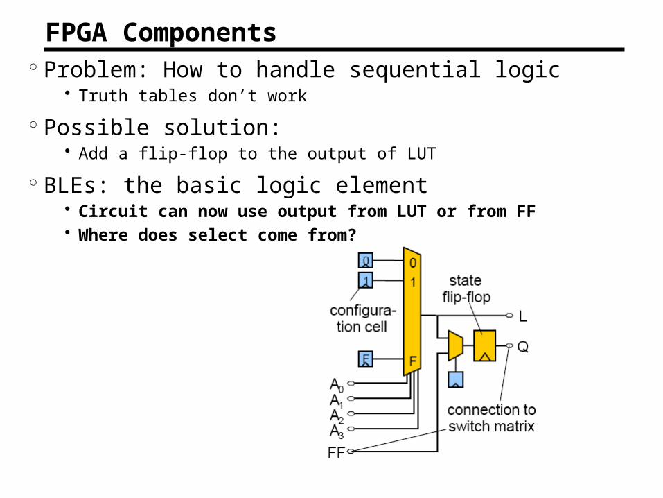
FPGA Components° Problem: How to handle sequential logic
• Truth tables don’t work
° Possible solution: • Add a flip-flop to the output of LUT
° BLEs: the basic logic element • Circuit can now use output from LUT or from FF• Where does select come from?

FPGA Components° Example: 8-bit register using 3-input, 2-output LUTs
• Input: x, Output: y
3-in, 2-out LUT
FF FF

FPGA Components° Example: 8-bit register using 3-input, 2-output LUTs
• Input: x, Output: y° What does LUT need to do to implement register?
3-in, 2-out LUT
FF FF
3-in, 2-out LUT
FF FF
3-in, 2-out LUT
FF FF
3-in, 2-out LUT
FF FF
x(7) x(6) x(5) x(4) x(3) x(2) x(1) x(0)
y(7) y(6) y(5) y(4) y(3) y(2) y(1) y(0)

FPGA Components• LUT simply passes inputs to appropriate output
3-in, 2-out LUT
FF FF
x(1) x(0)
y(1) y(0)
x2 x1 x0 o1 o0
FF FF
x(1) x(0)
y(1) y(0)
Inputs/Outputs LUT functionality

FPGA Components• LUT simply passes inputs to appropriate output
3-in, 2-out LUT
FF FF
x(1) x(0)
y(1) y(0)
FF FF
x(1) x(0)
y(1) y(0)
Inputs/Outputs LUT functionality
x2 x1 x0 o1 o0
0 0 0 0 0
0 0 1 0 1
0 1 0 1 0
0 1 1 1 1
1 0 0 0 0
1 0 1 0 1
1 1 0 1 0
1 1 1 1 1

FPGA Components° Isn’t it a waste to use LUTs for registers?° YES! (when it can be used for something else)
• Commonly used for pipelined circuits- Example: Pipelined adder
3-in, 2-out LUT
FF FF
+
Register
+
+
Register
Register
3-in, 2-out LUT
FF FF
. . . .
Adder and output register combined – not a separate LUT for each

FPGA Components° Configurable Logic Blocks (CLBs) usually contain more
than 1 BLE• Why?
- Efficient way of handling common I/O between adjacent LUTs- Saves routing resources
3-in, 2-out LUT
FF
2x1
FF
2x1
3-in, 2-out LUT
FF
2x1
FF
2x1
2x1
CLB

FPGA Components° Example: Ripple-carry adder
• Each LUT implements 1 full adder• Use efficient connections between LUTs for carry signals
3-in, 2-out LUT
FF
2x1
FF
2x1
3-in, 2-out LUT
FF
2x1
FF
2x1
2x1
CLB
A(0) B(0) Cin(0)
S(0)
Cin(1)
A(1) B(1)
S(1)
Cout(0)
Cout(1)

FPGA Components
° On real FPGAs: a cluster of LUTs per switch matrix (e.g., eight LUTs and switch matrix form a configurable logic block on Xilinx FPGAs)

Typical CLB° The arithmetic logic provides
• XOR-gate and faster carry chain to build faster adder without wasting too much LUT-resources.
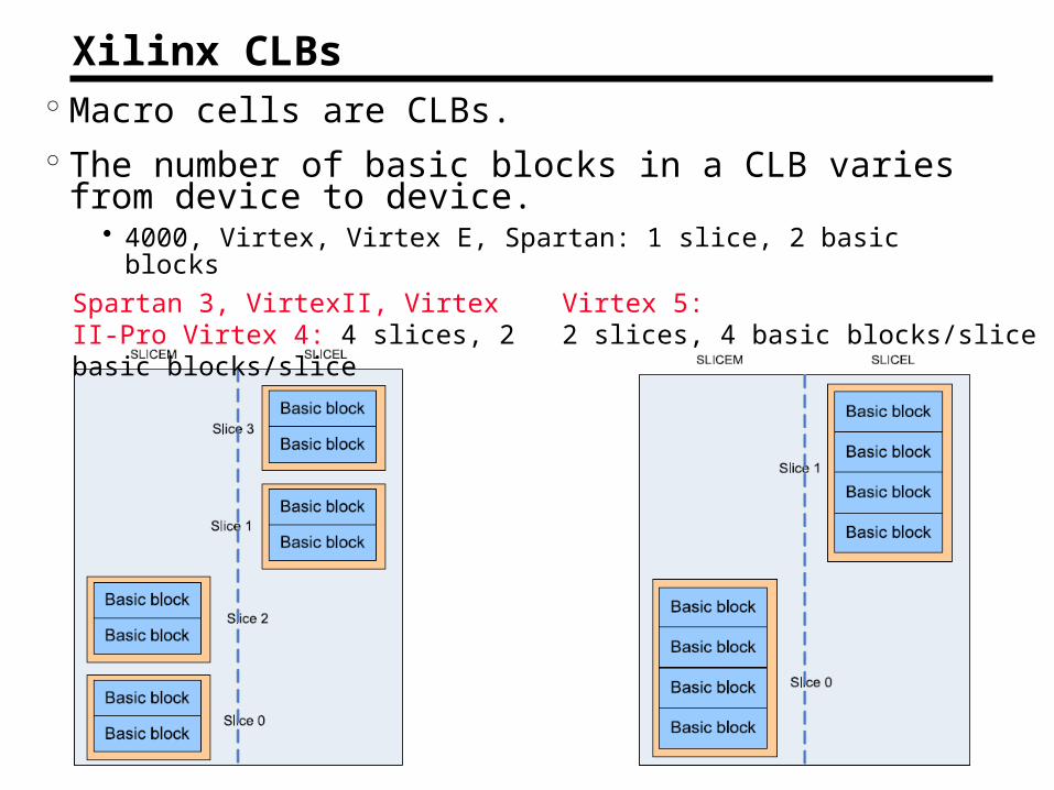
Xilinx CLBs° Macro cells are CLBs. ° The number of basic blocks in a CLB varies from device
to device. • 4000, Virtex, Virtex E, Spartan: 1 slice, 2 basic blocks
Virtex 5: 2 slices, 4 basic blocks/slice
Spartan 3, VirtexII, Virtex II-Pro Virtex 4: 4 slices, 2 basic blocks/slice

Xilinx CLBs° Left part slices of a CLB (SLICEM)
• configured either as combinatorial logic or SRAM or shift register
° SLICEL• only to be configured as combinatorial logic.
° Each BLE• 4 inputs and 1 output
Spartan 3, VirtexII, Virtex II-Pro Virtex 4: 4 slices, 2 basic blocks/slice

Xilinx CLBs° LUT has 6 inputs and 2 outputs. ° LUT can be configured either as
• a 6-input LUT, in which case only one output can be used, • or as two 5-input LUTs, two outputs used
Virtex 5: 2 slices, 4 basic blocks/slice

Xilinx Virtex6 CLB° A CLB contains 2 identical slices on Virtex 6
• 2 slices are split in two columns of 1 slices each
° 1 slice contains: • 4x 6-inputs LUT • 8x FF for storing LUT results • MUX to feed LUT either to a FF or the output • Carry in and carry out to construct fast adder using neighbor CLBs

Xilinx Virtex6 CLB

Altera FPGA Basic Blocks° Altera’s FPGAs (Cyclone, FLEX)
• basic unit of logic is the logic element (LE)• also LUT-based• a 4-LUT, a flip flop, a multiplexer and additional logic for carry chain • LEs can operate in different modes each of which defines different usage
of the LUT inputs.
° Altera LEs • grouped into logic array blocks (LAB). • Flex 6000 LAB contains 10 LEs• FLEX 8000 LAB contains 8 LEs. • Cyclone II LAB contains 16 LEs

Altera FPGA Basic Blocks° Stratix II
• basic computing unit is called adaptive logic module (ALM) • Each LAB contains 8 ALMs• ALM can be used to implement functions with variable number of inputs. • Ensures a backward compatibility to 4-input-based designs, • Possible to implement module with up to 8 inputs. • Additional modules: including flip flops, adders and carry logic

FPGA Components° CLBs often have specialized connections between
adjacent CLBs• Further improves carry chains• Avoids routing resources
° Basic building block is CLB• Can implement combinational+sequential logic• All circuits consist of combinational and sequential logic
° So what else is needed?• FPGAs need some way of connecting CLBs together
- Reconfigurable interconnect- But, we can only put fixed wires on a chip

FPGA Components° Problem: If FPGA doesn’t know which CLBs will be
connected, where does it put wires?• Solution:
- Put wires everywhere!– Referred to as channel wires, routing channels, routing tracks,
many others- CLBs typically arranged in a grid, with wires on all sides
CLB CLB CLB
CLB CLB CLB

FPGA Components°How to connect CLB to wires?°Solution: Connection box
• Device that allows inputs and outputs of CLB to connect to different wires
CLB CLB
Connection box
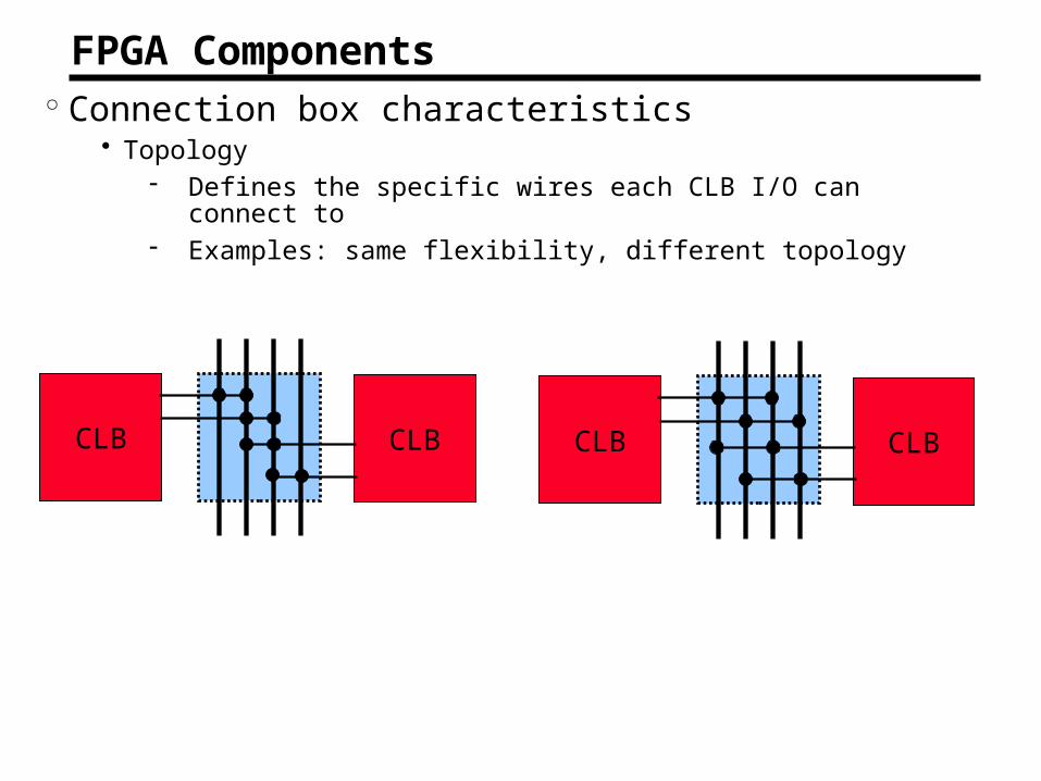
FPGA Components° Connection box characteristics
• Topology- Defines the specific wires each CLB I/O can connect to- Examples: same flexibility, different topology
CLB CLB CLB CLB

FPGA Components° Connection boxes allow CLBs to connect to routing wires
• But, that only allows us to move signals along a single wire• Not very useful
° How do FPGAs connect wires together?

FPGA Components°Solution: Switch boxes, switch matrices
• Connects horizontal and vertical routing channels- But, we can only put fixed wires on a chip
CLB CLB
CLB CLB
Switch box/matrix
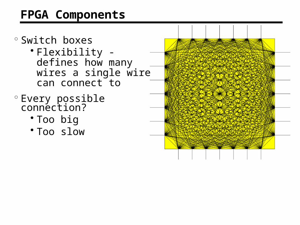
FPGA Components
° Switch boxes• Flexibility - defines how
many wires a single wire can connect to
° Every possible connection?• Too big• Too slow

FPGA Components° Why do flexiblity and topology matter?
• Routability: a measure of the number of circuits that can be routed
- Higher flexibility = better routability- Wilton switch box topology = better routability
CLB CLB
Src
Dest
Dest
Src
No possible route from src to dest

FPGA Components° Many Topologies possible
• Fs = 3 is common
° Topology - defines which wires can be connected
0 1 2 3 4 5 6
0 1 2 3 4 5 6
0 1 2 3 4 5 6
0 1 2 3 4 5 6
Disjoint Wilton Universal

FPGA Components
° Disjoint: a wire entering can only connect to other wires with the same numerical designation.
• potential source–destination routes in the FPGA are isolated into distinct routing domains, limiting routing flexibility.
° Wilton: uses same number of routing switches but overcomes the domain issue
• By allowing for a change in domain assignment on connections that turn.
• ability to change domains in at least one direction facilitates routing as a greater diversity of routing paths from a net source to a destination is possible.
0 1 2 3 4 5 6
0 1 2 3 4 5 6
0 1 2 3 4 5 6
0 1 2 3 4 5 6G. Lemieux and D. Lewis, “Circuit design of routing switches,” in Proceedings: ACM/SIGDA International Symposium on Field Programmable Gate Array, pp. 19–28, February 2002.G. Lemieux and D. Lewis, Design and Interconnection Networks for Programmable Logic. Boston, MA: Kluwer Academic Publishers, 2004.

FPGA Components°At each switch block: some tracks end some
tracks pass right through

FPGA Components°Switch boxes
• Short channels- Useful for connecting adjacent CLBs
• Long channels- Useful for connecting CLBs that are separated- Allows for reduced routing delay for non-adjacent CLBs
MediumShort
Long

FPGA Components° FPGA layout called a “fabric”
• 2-dimensional array of CLBs and programmable interconnect• Sometimes referred to as an “island style” architecture

FPGA and Data Storage°Solution 1: Use LUTs for logic or memory
• LUTs are just an SRAM• Xilinx refers to as distributed RAM
°Solution 2: Include dedicated RAM components in the FPGA fabric
• Xilinx refers to as Block RAM- Can be single/dual-ported- Can be combined into arbitrary sizes- Can be used as FIFO
– Different clock speeds for reads/writes

FPGA Components° Fabric with Block RAM
• Block RAM can be placed anywhere• Typically, placed in columns of the fabric
CLB CLB
CLB CLB
CLB
CLB
CLB
CLB
CLB CLB CLB CLB
BR
BR
BR
BR
BR
BR
. . .
. . . .

FPGA Components° FPGAs commonly used for DSP apps
• Makes sense to include custom DSP units instead of mapping onto LUTs
- Custom unit = faster/smaller
° Example: Xilinx DSP48• Starting with Virtex 4 family, Xilinx introduced DSP48 block for high-
speed DSP on FPGAs• Essentially a multiply-accumulate core with many other features• Provides efficient way of implementing
- Add/subtract/multiply- MAC (Multiply-accumulate)- Barrel shifter- FIR Filter- Square root

FPGA Components° FPGAs are 2-dimensional arrays of CLBs, DSP, Block RAM, and
programmable interconnect• Actual layout/placement differs for different FPGAs
DSP DSP DSP DSPBR BR
CLB CLB
CLB CLB
CLB
CLB
CLB
CLB
CLB CLB CLB CLB
BR
BR
BR
BR
BR
BR
. . . .

FPGA Components
Xilinx Virtex II Pro FPGA

Spartan3 Components
Spartan 3
RAM blocks
Multipliers
Logic blocks

Spartan3 Components

Spartan3 Components

FPGA Components
x
+
x
+
A[n:0]
B[n:0] Y[(2n - 1):0]
Multiplier
Adder
Accumulator
MAC

Virtex7 FPGA DSP48
DSP48E1 Tile (Two DSP48E1 Slices and Interconnects)

Virtex7 FPGA DSP48° Single-instruction-multiple-data (SIMD) arithmetic unit:
• Dual 24-bit or quad 12-bit add/subtract/accumulate° Cascading capability on both pipeline paths for larger
multipliers and larger post-adders

Virtex7 FPGA DSP48

Zynq FPGA Components

Zynq FPGA Components

Zynq FPGA Components
Programming FPGAs
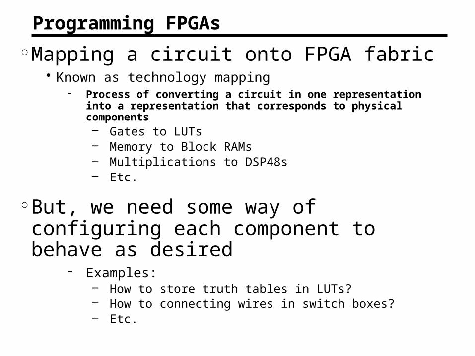
°Mapping a circuit onto FPGA fabric• Known as technology mapping
- Process of converting a circuit in one representation into a representation that corresponds to physical components – Gates to LUTs– Memory to Block RAMs– Multiplications to DSP48s– Etc.
°But, we need some way of configuring each component to behave as desired
- Examples:– How to store truth tables in LUTs?– How to connecting wires in switch boxes?– Etc.

Programming FPGAs° FPGAs programmed with a “bitfile”
• File containing all information needed to program FPGA- Contains bits for each control FF- Also, contains bits to fill LUTs
° But, how do you get the bitfile into the FPGA?• > 10k LUTs• Small number of pins
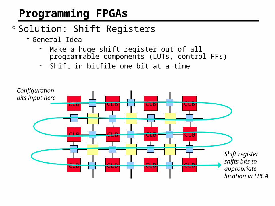
Programming FPGAs° Solution: Shift Registers
• General Idea- Make a huge shift register out of all programmable components
(LUTs, control FFs)- Shift in bitfile one bit at a time
CLB CLB
CLB CLB
CLB
CLB
CLB
CLB
CLB CLB CLB CLB
Configuration bits input here
Shift register shifts bits to appropriate location in FPGA

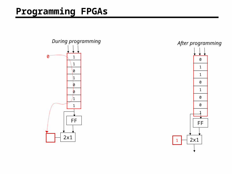
Programming FPGAs° Example:
• Program CLB with 3-input, 1-output LUT to implement sum output of full adder
In Out
A B Cin S
0 0 0 0
0 0 1 1
0 1 0 1
0 1 1 0
1 0 0 1
1 0 1 0
1 1 0 0
1 1 1 1
FF
2x11
0
1
1
0
1
0
0
1
Should look like this after programming
FF
2x11
0
1
1
0
1
0
0
1
Assume data is shifted in this direction

Programming FPGAs° Example, Cont:
• Bitfile is just a sequence of bits based on order of shift register
FF
2x1
011010011
FF
2x11
0
1
1
0
1
0
0
1
During programming After programming

Programming FPGAs
FF
2x11
0
1
1
0
1
0
0
1
After programming
FF
2x1
101101001
During programming

Programming FPGAs
FF
2x11
0
1
1
0
1
0
0
1
After programming
FF
2x1
1
1
0110100
During programming

Programming FPGAs
FF
2x11
0
1
1
0
1
0
0
1
After programming
FF
2x1
0
1
1
011010
During programming

Programming FPGAs
FF
2x11
0
1
1
0
1
0
0
1
After programming
FF
2x1
0
0
1
1
01101
During programming

Programming FPGAs
FF
2x11
0
1
1
0
1
0
0
1
After programming
FF
2x1
1
0
0
1
1
0110
During programming

Programming FPGAs
FF
2x11
0
1
1
0
1
0
0
1
After programming
FF
2x1
0
1
0
0
1
1
011
During programming

Programming FPGAs
FF
2x11
0
1
1
0
1
0
0
1
After programming
FF
2x1
1
0
1
0
0
1
1
01
During programming
Programming FPGAs
FF
2x11
0
1
1
0
1
0
0
1
After programming
FF
2x1
1
1
0
1
0
0
1
1
0
During programming

Programming FPGAs
FF
2x11
0
1
1
0
1
0
0
1
After programming
FF
2x1
0
1
1
0
1
0
0
1
During programming
1
CLB is programmed to implement full adder!
Easily extended to program entire FPGA

Programming FPGAs
°Problem: Reconfiguring FPGA is slow• Shifting in 1 bit at a time not efficient• Bitfiles can be greater than 1 MB• Eliminates one of the main advantages of RC
- Partial reconfiguration- With shift registers, entire FPGA has to be reconfigured

FPGA Components° High-performance families
• Virtex (220 nm)• Virtex-E, Virtex-EM (180 nm)• Virtex-II (130 nm)• Virtex-II PRO (130 nm)• Virtex-4 (90 nm)• Virtex-5 (65 nm)• Virtex-6 (40 nm)• Virtex-7 (28 nm)
° Low Cost Family• Spartan/XL – derived from XC4000• Spartan-II – derived from Virtex• Spartan-IIE – derived from Virtex-E• Spartan-3 (90 nm)• Spartan-3E (90 nm) – logic optimized• Spartan-3A (90 nm) – I/O optimized• Spartan-3AN (90 nm) – non-volatile, • Spartan-3A DSP (90 nm) – DSP optimized• Spartan-6 (45 nm)• Artix-7 (28 nm)

CPLD vs FPGA
° Simpler interconnect structure • Timing performance more predictable than FPGAs.
° Density is less than most FPGAs • CPLDs feature logic resources with a wide number of inputs (AND planes)
° Performance is usually better than FPGAs
° A single FPGA can replace tens of normal PLDs• Primitive FPGA 'logic cells' are more complex than PLD cells.
• Can program the routing between FPGA logic cells in addition to programming the logic cells themselves.
• Many FPGAs now offer embedded memory blocks in addition to logic blocks or other special features such as fast carry logic chains.
° FPGAs offer a higher ratio of flip-flops to logic resources than do CPLDs.