ece c03 lecture 61 lecture 6 delays and timing in multilevel logic synthesis prith banerjee ece c03...
Post on 21-Dec-2015
215 views
TRANSCRIPT
ECE C03 Lecture 6 1
Lecture 6Delays and Timing in Multilevel Logic
Synthesis
Prith Banerjee
ECE C03
Advanced Digital Design
Spring 1998

ECE C03 Lecture 6 2
Outline
• Gate delays• Timing waveforms• Performance calculations• Static/dynamic hazards and glitches• Designs to avoid hazards• READING: Katz 3.3, 3.4, 3.5.2, Dewey 6.5.1,
6.5.2
ECE C03 Lecture 6 3
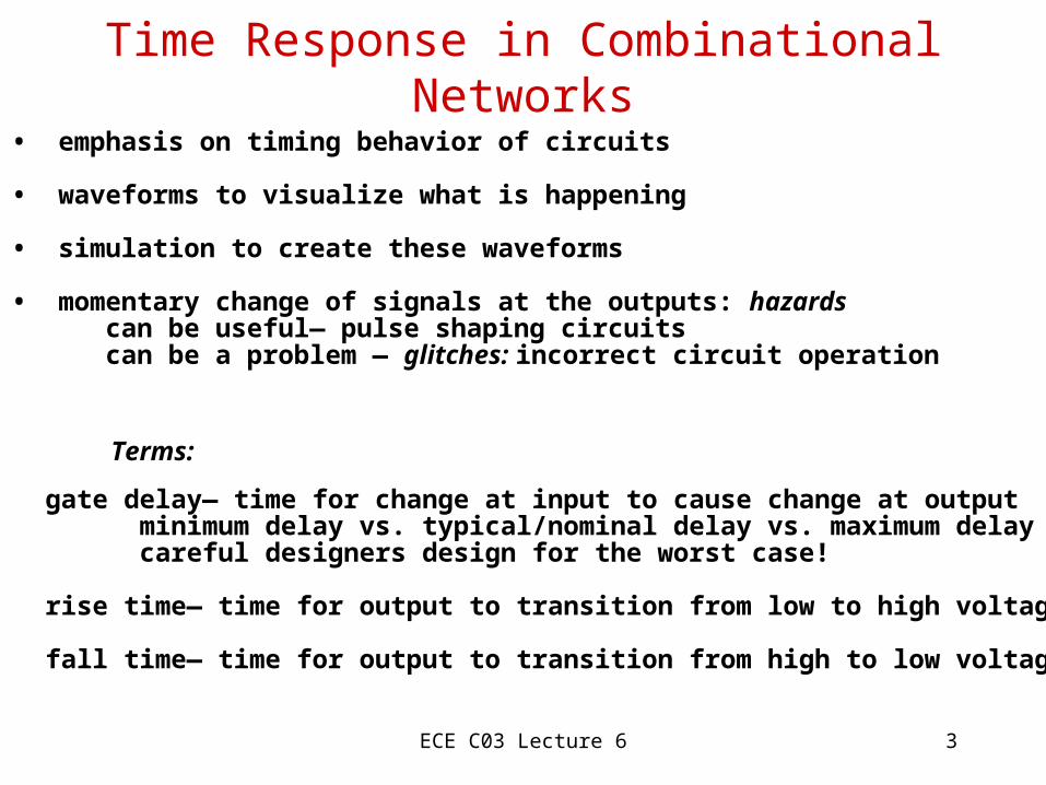
Time Response in Combinational Networks
• emphasis on timing behavior of circuits
• waveforms to visualize what is happening
• simulation to create these waveforms
• momentary change of signals at the outputs: hazards can be useful— pulse shaping circuits can be a problem — glitches: incorrect circuit operation
Terms:
gate delay— time for change at input to cause change at output minimum delay vs. typical/nominal delay vs. maximum delay careful designers design for the worst case!
rise time— time for output to transition from low to high voltage
fall time— time for output to transition from high to low voltage
ECE C03 Lecture 6 4
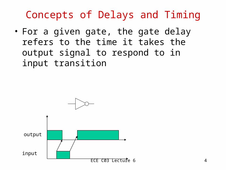
Concepts of Delays and Timing
• For a given gate, the gate delay refers to the time it takes the output signal to respond to in input transition
input
output

ECE C03 Lecture 6 5
Gate Delays
• Why is there a gate delay?• There are actual resistances and capacitances
inside digital logic• If you apply a unit step voltage signal to an input,
the output will not respond immediately, but after a delay proportional to R.C
Input OutputCapacitanceof load
Resistance of driverT delay = R.C
ECE C03 Lecture 6 6
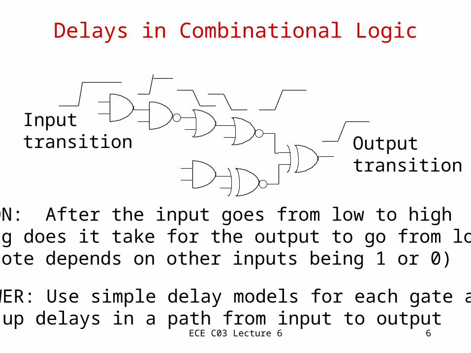
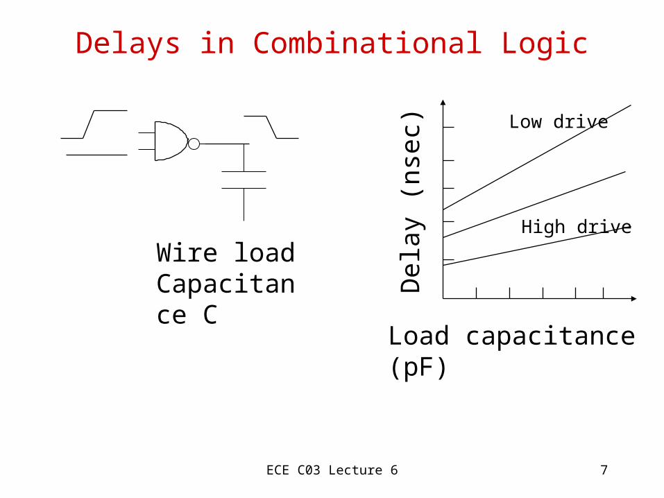
Delays in Combinational Logic
Inputtransition Output
transition
QUESTION: After the input goes from low to highhow long does it take for the output to go from low tohigh (note depends on other inputs being 1 or 0)
ANSWER: Use simple delay models for each gate andadd up delays in a path from input to output
ECE C03 Lecture 6 7
Delays in Combinational Logic
Wire loadCapacitance C
Load capacitance(pF)
Del
ay (
nsec
)
Low drive
High drive

ECE C03 Lecture 6 8
Designing Logic With High Performance
Inputtransition
QUESTION: Suppose the delay from input to output is 30 nsecand is unacceptable. How would you make a higher performancedesign?ANSWER: Reduce capacitances at various loads,or use higher druve gates
Reduce high load due to fanout
Higher drive gate

ECE C03 Lecture 6 9
Gate Delays for Typical TTL Families
TTL Family MaximumtpHL
MaximumtpLH
MinimumtpHL
MinimumtpLH
7400 15 22 7 11
74H00 10 10 6.2 5.9
74L00 60 60 31 35
Delays in nano-seconds

ECE C03 Lecture 6 10
Example gate delays in nanoseconds for LSI Logic 1.5 micron gate array2 input AND gate.
tpLH = Propagation delay from low to high transition at outputtpHL = Propagation delay from high to low transition at output
Gate Delay Specifications
STD LOAD 1 2 3 4 8 16
tpLH 0.7 0.8 1.0 1.2 1.8 3.2
tpHL 0.9 1.0 1.0 1.1 1.3 1.8
ECE C03 Lecture 6 11
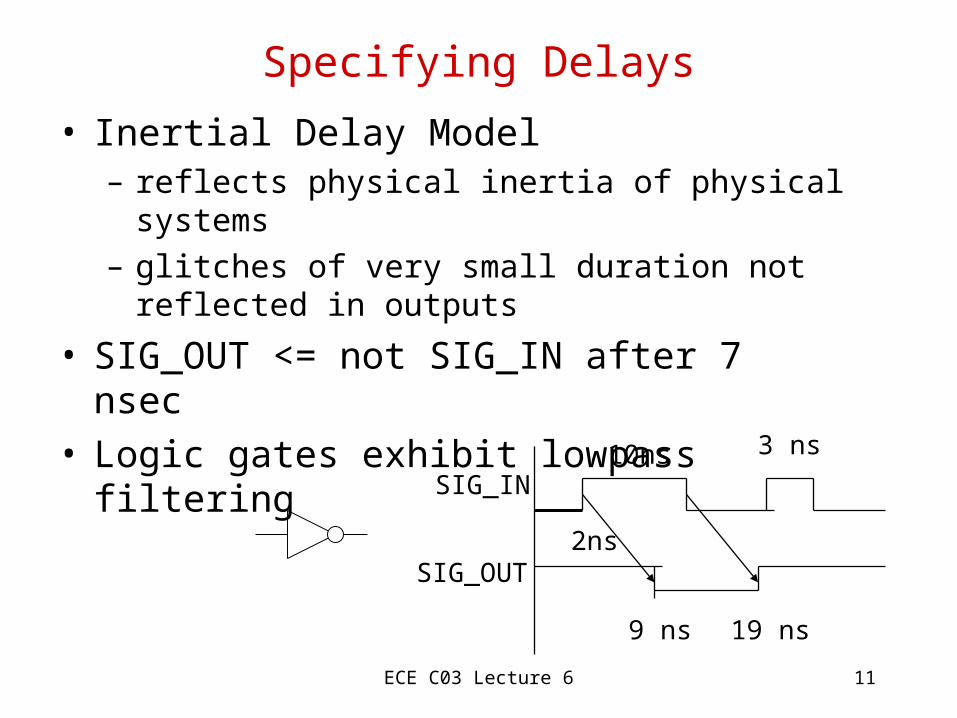
Specifying Delays
• Inertial Delay Model– reflects physical inertia of physical systems
– glitches of very small duration not reflected in outputs
• SIG_OUT <= not SIG_IN after 7 nsec• Logic gates exhibit lowpass filtering
SIG_IN
SIG_OUT2ns
9 ns 19 ns
3 ns10ns
ECE C03 Lecture 6 12
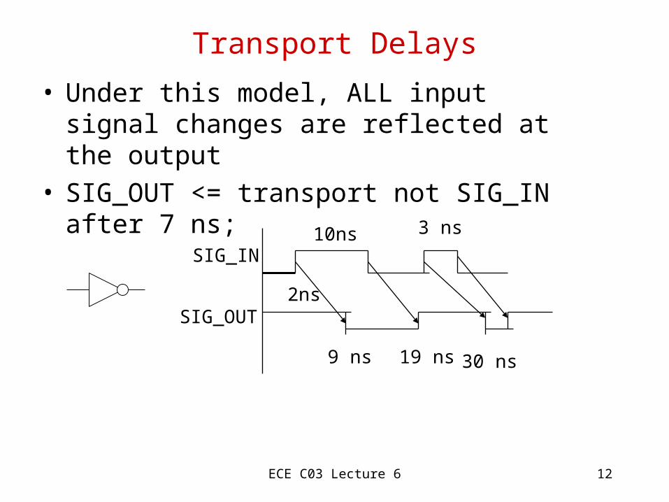
Transport Delays
• Under this model, ALL input signal changes are reflected at the output
• SIG_OUT <= transport not SIG_IN after 7 ns;
SIG_IN
SIG_OUT2ns
9 ns 19 ns
3 ns10ns
30 ns
ECE C03 Lecture 6 13
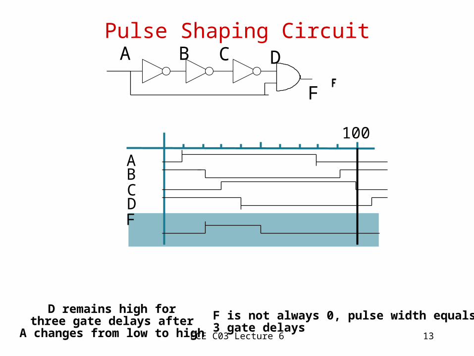
Pulse Shaping Circuit
F is not always 0, pulse width equals3 gate delays
D remains high forthree gate delays after
A changes from low to high
100
A B C D F
A B C D
F
ECE C03 Lecture 6 14
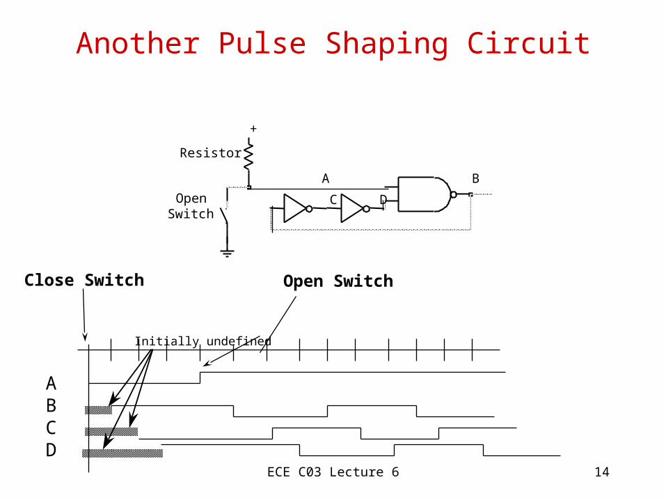
Another Pulse Shaping Circuit
Initially undefined
Close Switch Open Switch
+
A B
C DOpenSwitch
Resistor
ABCD
ECE C03 Lecture 6 15
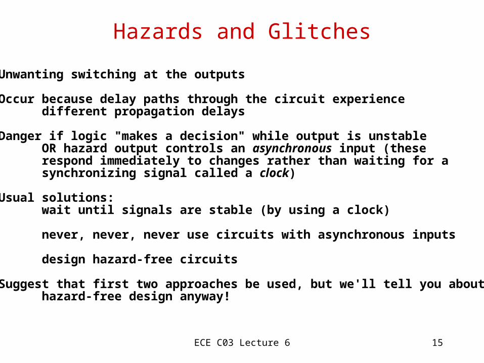
Hazards and Glitches
Unwanting switching at the outputs
Occur because delay paths through the circuit experience different propagation delays
Danger if logic "makes a decision" while output is unstable OR hazard output controls an asynchronous input (these respond immediately to changes rather than waiting for a synchronizing signal called a clock)
Usual solutions: wait until signals are stable (by using a clock)
never, never, never use circuits with asynchronous inputs
design hazard-free circuits
Suggest that first two approaches be used, but we'll tell you about hazard-free design anyway!

ECE C03 Lecture 6 16
Kinds of Hazards
Kinds of Hazards
Input change causes output to go from 1 to 0 to 1
Input change causes output to go from 0 to 1 to 0
Input change causes a double change from 0 to 1 to 0 to 1 OR from 1 to 0 to 1 to 0
Static 0-hazard
Dynamic hazards
Static 1-hazard
1 1
0
1
0 0
1
0 0
1
1 1
0 0
ECE C03 Lecture 6 17
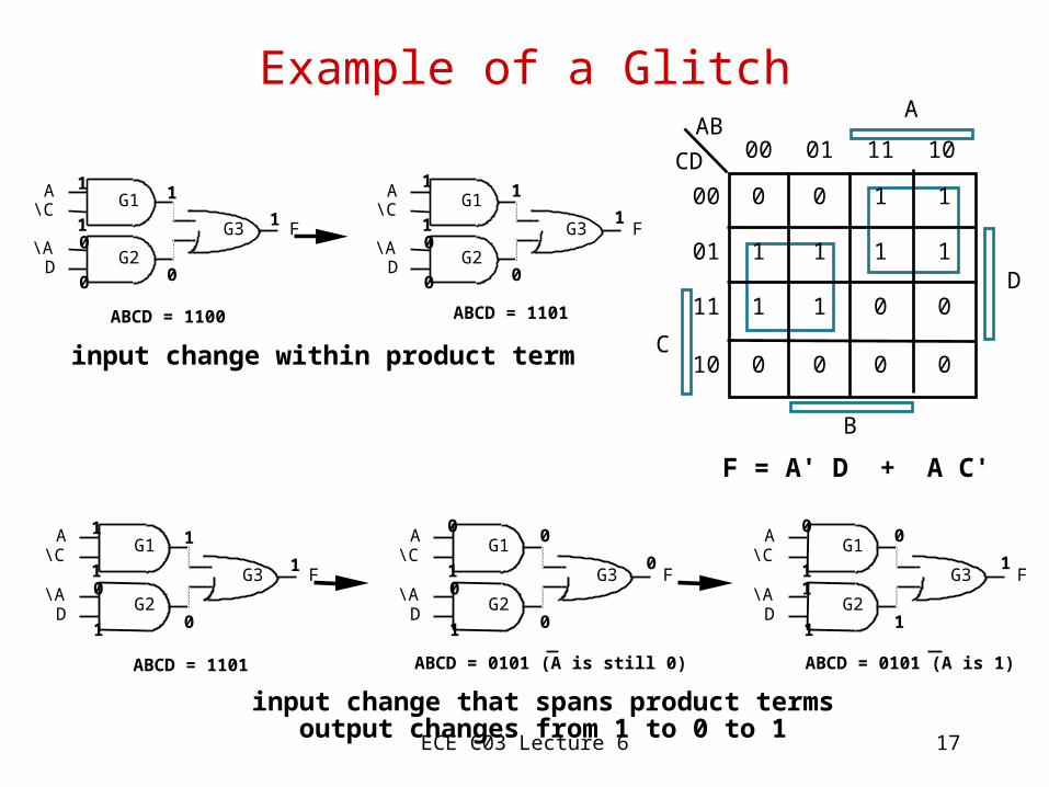
Example of a Glitch
F = A' D + A C'
input change within product term
input change that spans product termsoutput changes from 1 to 0 to 1
G1
G2
G3
A\C
\AD
F
G1
G2
G3
A\C
\AD
F
1
1
1
1
0
0
0
1
1
1
1
0
0
0
ABCD = 1100 ABCD = 1101
G1
G2
G3
A\C
\AD
F
G1
G2
G3
A\C
\AD
F
0
1
0
0
1
0
0
1
1
1
1
1
0
0
ABCD = 1101 ABCD = 0101 (A is still 0)
G1
G2
G3
A\C
\AD
F
0
1
0
1
1
1
1
ABCD = 0101 (A is 1)
A AB
00 01 11 10
0 0 1 1
1 1 1 1
1 1 0 0
0 0 0 0
00
01
11
10 C
CD
D
B

ECE C03 Lecture 6 18
Eliminating Glitches
General Strategy: add redundant terms
F = A' D + A C' becomes A' D + A C' + C' D
This eliminates 1-hazard? How about 0-hazard?
Re-express F in PoS form:
F = (A' + C')(A + D)
Glitch present!
Add term: (C' + D)
This expression is equivalentto the hazard-free SoP form of F
A AB
00 01 11 10
0 0 1 1
1 1 1 1
1 1 0 0
0 0 0 0
00
01
11
10 C
CD
D
B

ECE C03 Lecture 6 19
How to design Circuits without Glitches
Start with expression that is free of static 1-hazards
F = A C' + A' D + C' D
F' = (A C' + A' D + C' D)'
= (A' + D) (A + D') (C + D')
= A C + A C D' + C D' + A' C D' + A' D'
= A C + C D' + A' D'
covers all the adjacent 0's in the K-map
free of static-1 and static-0 hazards!
Work with complement:

ECE C03 Lecture 6 20
Detecting Static Hazards in Multilevel Circuits
Calculate transient output function
variables and complements are treated as independent variables
cannot use X + X' = 1 or X • X' = 0 for simplifications
F = A B C + (A + D) (A' + C')
F1 = A B C + A A' + A C' + A' D + C' D
Example:
2-level form
ABCD: 1111 to 1110, covered by term ABC, so no 1-hazard present
ABCD: 1110 to 1100, term ABC goes low while term AC' goes high
some static hazards are present!
A AB
00 01 11 10
0 0 1 1
1 1 1 1
1 1 1 0
0 0 1 0
00
01
11
10 C
CD
D
B
ECE C03 Lecture 6 21
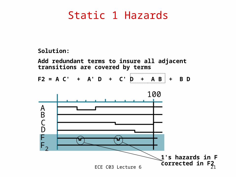
100
A B C D F F 2
Static 1 Hazards
Solution:
Add redundant terms to insure all adjacent transitions are covered by terms
F2 = A C' + A' D + C' D + A B + B D
1's hazards in Fcorrected in F2

ECE C03 Lecture 6 22
Static 0 Hazards
Similar to previous case, but work with the complement of F
If terms of the transient output function cover all 0 transitions, then no 0-hazards are present
F = [A B C + (A + D) (A' + C')]'
= (A' + B' + C') (A' D' + A C)
= A' D' + A' B D' + A' C D' + A B' C
= A' D' + A B' C
0-hazard on transition from1010 to 0010
+ B' C D'
F = (A + D) (A' + B + C') (B + C' + D)
0-hazard free
equivalent to F2 on last slide
A AB
00 01 11 10
0 0 1 1
1 1 1 1
1 1 1 0
0 0 1 0
00
01
11
10 C
CD
D
B

ECE C03 Lecture 6 23
100
A B C D F F 3
Static 0 Hazards
0-HazardCorrected in F3

ECE C03 Lecture 6 24
Designing Networks for Hazard Free Operation
Simply place transient output function in a form that guarantees that all adjacent ones are covered by a term
no term of the transient output function contains both a variable and its complement
F(A,B,C,D) = m(1,3,5,7,8,9,12,13,14,15)
F = A B + A' D + B D + A C' + C' D
= (A' + B + C') D + A (B + C')
(factored by distributive law, which does notintroduce hazards since it does not depend onthe complementarity laws for its validity)
A AB
00 01 11 10
0 0 1 1
1 1 1 1
1 1 1 0
0 0 1 0
00
01
11
10 C
CD
D
B
ECE C03 Lecture 6 25
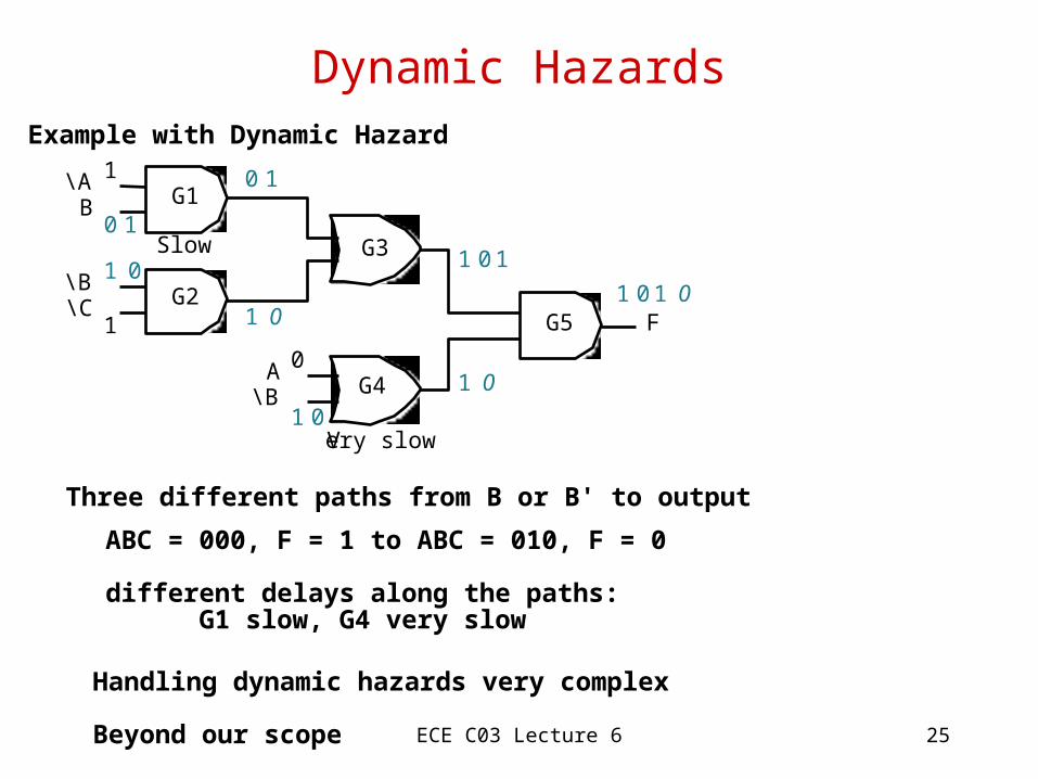
Dynamic HazardsExample with Dynamic Hazard
Three different paths from B or B' to output
ABC = 000, F = 1 to ABC = 010, F = 0
different delays along the paths: G1 slow, G4 very slow
Handling dynamic hazards very complex
Beyond our scope
G1
G2
G3
G5
G4
\A B
\B
\B \C
F
A
0 1
1
1 0
1
0 1
1 0
1 0 1
1 0 0
1 0
1 0 1 0
Slow
V ery slow

ECE C03 Lecture 6 26
Summary
• Gate delays• Timing waveforms• Performance calculations• Static/dynamic hazards and glitches• Designs to avoid hazards• NEXT LECTURE: Multilevel Logic Synthesis• READING: Katz 3.1, 3.2