ed-4701 300-3 e 表紙 - jeita · eiaj ed-4701/300-3 - 7 - (b) baking performed before dry packing...
TRANSCRIPT

JEITA Standard of Japan Electronics and Information Technology Industries Association
EIAJ ED-4701/300-3
Environmental and endurance test methods for semiconductor devices
(Stress test I)
(Amendment 3)
Established in January, 2006
Investigated by
Technical Standardization Committee on Semiconductor Devices
Published by
Japan Electronics and Information Technology Industries Association

This document is a translation without guarantee. In the event of any doubt arising,
the original standard in Japanese is to be evidenced.
JEITA standards are established independently to any existing patents on the
products, materials or processes they cover.
JEITA assumes absolutely no responsibility toward parties applying these
standards or toward patent owners.
C 2006 by the Japan Electronics and Information Technology Industries Association
All rights reserved. No part of this standard may be reproduced in any form or by
any means without prior permission in writing from the publisher.

EIAJ ED-4701/300-3
CONTENTS
1. SCOPE ······································································································································ 1
2. DEFINITION OF TERMS ············································································································ 1
3. PRECAUTIONS ························································································································· 1
4. TEST METHODS ······················································································································· 1
COMMENTS ···································································································································· 2
APPENDIX
TEST METHOD 301B Resistance to soldering heat for surface mounting devices (SMD) ················ 4

EIAJ ED-4701/300-3
- 1 -
Standard of Japan Electronics and Information Technology Industries Association
Environmental and endurance test methods for semiconductor devices (Stress test I)
(Amendment 3)
1. SCOPE
Conforming to EIAJ ED-4701/300 “Environmental and endurance test methods for semiconductor devices
(Stress tests 1)”
2. DEFINITION OF TERMS
Conforming to EIAJ ED-4701/300
3. PRECAUTIONS
Conforming to EIAJ ED-4701/300
4. TEST METHODS
Conforming to EIAJ ED-4701/300
Remarks: The Process of deliberation and technical description of each test methods are given to the
test methods as Explanation.

EIAJ ED-4701/300-3
- 2 -
COMMENTS
1. PURPOSE OF ESTABLISHMENT OF THE AMENDMENT 3
It was recondite where the latest test methods was entered, it was resulting the confusion of users. So
establishment of new numbering system that was easy to use both users and manufacturers was decided,
and the standard has been established as EIAJ ED-4701/300 “Environment and endurance test methods
for semiconductor devices (Stress test I)” in August, 2001.
The change of a technical matter is needed in the test methods in part, we decided after that to publish
only the test methods of requiring change as the Amendment. However, every three years it will be
established as not the Amendment but the latest version of the standard “Environment and endurance
test methods for semiconductor devices (Stress test I)” that includes the whole test methods of
EIAJ ED-4701/300.
2. EVOLUTION OF THE DELIBERATIONS
The evolution of the deliberations is conformed to the explanation of each test methods.

EIAJ ED-4701/300-3
- 3 -
3. DELIBERATING MEMBERS
Deliberation of this standard has been made by “Sub-Committee on Semiconductor Devices Reliability” of
the Technical Standardization Committee on Semiconductor Devices/Semiconductor Devices Reliability
Group.
Below are listed the members of deliberation of this standard.
<Technical Standardization Committee on Semiconductor Devices/Semiconductor Devices Reliability Group>
Chairman Hisao Kasuga NEC Electronics Corp.
<Semiconductor Devices Reliability Group>
Chairman Kazutoshi Miyamoto Renesas Technology Corp.
<Sub-Committee on Semiconductor Devices Reliability>
Chairman Tetsuaki Wada Matsushita Electric Industrial Co.,Ltd.
Vice Chairman Junichi Mitsuhashi Renesas Technology Corp
Member Tadafumi Tashiro NEC Electronics Corp.
Yasuhito Anzai Oki Electric Industry Co., Ltd.
Osamu Nakayama Kawasaki Microelectronics, Inc.
Kazutoshi Kitazume Sanyo Electric Co., Ltd.
Makoto Kanayama Shindengen Electric Mfg. Co., Ltd.
Shinichi Ikezoe New Japan Radio Co., Ltd.
Hiroyoshi Odaira Seiko Epson Corp.
Kenji Sasaki Sony Corp.
Takumi Tanabe Toshiba Corp.
Yasuyuki Igarashi IBM Japan, Ltd.
Toshiki Yamaguchi Fujitsu Ltd.
Naohiro Yasuda Fuji Electric Holdings Co., Ltd.
Masashi Kusuda Mitsumi Electric Co., Ltd.
Kohki Ohara Ricoh Co., Ltd.
Takahiro Ito Rohm Co., Ltd.
Special Members Takeshi Watanabe NEC Electronics Corp
Yasuhiro Fukuda Oki Electric Industry Co., Ltd.
Kouji Obinata Sony Corp.

EIAJ ED-4701/300-3
- 4 -
TEST METHOD 301B Resistance to soldering heat for surface
mounting devices (SMD)
1. SCOPE
This standard provides for the method to evaluate to soldering heat of SMD used in electronic equipment
for consumer application and industrial application in general. This standard is also applicable to both
Sn-Pb solder paste and Pb free solder paste.
2. APPARATUS
2.1 High temperature furnace
The high temperature furnace must be capable of keeping temperature specified in Sub-clause 4.2 for long
time.
2.2 Moisture chamber
The moisture chamber must be capable of keeping temperature and relative humidity specified in Sub-
clause 4.3 for long time. The material composing the chamber must not react under high humidity
conditions. Water to be used in the tests must be distilled water or deionized water, with pH from 6.0 to 7.2
and resistivity of 500Ωm or more at 23°C.
2.3 Infrared reflow soldering/Convection reflow soldering furnace
The infrared and the convection reflow soldering furnace must be capable to meet the temperature profile
specified in Sub-clause 4.4(1). The temperature profile is specified in terms of the temperature of top
surface of the specimen placed on the holder (refer to Sub-clause 2.7). The temperature at the top surface
of the specimen shall be measured as shown in Figure 1. However, in the case of area array package
such as BGA, the temperature can also be measured as shown in Figure 2(a) or Figure 2(b).
Figure 1 Method of measuring the temperature profile of a specimen

EIAJ ED-4701/300-3
- 5 -
(a) Area array package 1 (b) Area array package 2
Figure 2 Method of measuring the temperature profile of a specimen (area array package)
2.4 Vapor phase reflow soldering furnace
The vapor phase reflow soldering furnace must be capable to meet the temperature profile specified in
Sub-clause 4.4(2). The temperature profile is specified in terms of the temperature of top surface of the
specimen placed on the holder (refer to Sub-clause 2.7). The temperature at the top surface of the
specimen shall be measured as shown in Figure 1. However, in the case of area array package such as
BGA, the temperature can be measured as shown in Figure 2(a) or Figure 2(b).
2.5 Wave soldering furnace
The wave soldering furnace must be capable of keeping temperature of molten solder during the solder
heating specified in Sub-clause 4.4(3). The molten solder must always be flowed. The preheat conditions
in Sub-clause 4.4(3)(b) are specified in terms of the temperature at the top surface of the specimen as
shown in Figure 1 or Figure 2(a) or Figure 2(b).
2.6 Solder bath
The solder bath should have capacity enough to keep the temperature of molten solder within the
prescribed values even during the solder heating described in Sub-clause 4.4(4). The dipping equipment
should be capable to control the dipping depth and the dipping time of the terminals in the molten solder
as specified in Sub-clause 4.4(4)(c).
2.7 Holders
Unless otherwise specified, the material of the holder, which the specimen is to be placed on during the
solder heating in the reflow soldering and the wave soldering furnace, should be made from glass-
reinforced epoxy resin, polyimide, or alumina substrate.
3. MATERIALS
3.1 Perfluorocarbon
Use Perfluorocarbon (perfluoroisobutyrene) or equivalent in vapor phase reflow soldering furnaces.
Adhesive agent or thin heat-proof tape
Die
Resin
Solder ball
Holder
Thermocouple
Holder
Adhesive agent or thin heat-proof tape
Thermocouple

EIAJ ED-4701/300-3
- 6 -
3.2 Solder
Solders to be used in this test should be those ones specified in H60A, H60S, H63A of JIS Z 3282
(SOLDER) or in APPENDIX B of JIS C 0050. Unless otherwise specified in the relevant specification,
solder paste of Sn-Ag-Cu is used.
3.3 Flux
Flux to be used in this test should be 2-propanol (JIS K 8839) or ethanol (ethyl alcohol, JIS K 8101)
solution of rosin (JIS K 5902) (the concentration should be from 10% to 35% of rosin in terms of mass ratio,
and 25% unless otherwise specified) or the material specified in APPENDIX C of JIS C 0050.
4. TEST PROCEDURE
4.1 Initial measurement
In accordance with the relevant specification, the electrical characteristics of the specimen shall be
measured, and the visual inspection for cracks and the other defects of the specimen shall be made with
the assistance of a magnifier capable of giving 40 magnifications. The initial appearance for cracks and
delaminations of inside of the specimen shall be inspected using scanning acoustic tomography (SAT) if
necessary. (refer Sub-clause 4.6)
4.2 Baking
Unless otherwise specified in the relevant specification, baking under conditions of 125±5°C for 24h or
more shall be performed if moisture soaking specified in Sub-clause 4.3 will be performed.
4.3 Moisture soaking
Moisture soaking specified in (1) or (2) of this Sub-clause shall be performed if the specimen is type of
resin encapsulated SMD. The baking treatment specified in the relevant specification shall be performed
instead of the moisture soaking if the baking before real soldering of electronic assembly process is
specified in the relevant specification. Unless otherwise specified in the relevant specification, the solder
heating specified in Sub-clause 4.4 shall be started within 4h(1) after finishing this moisture soaking.
Note (1): Longer time than 4h can be specified in the relevant specification if the specimen is a thicker
SMD because it does not affect the moisture absorption and the drying.
(1) Moisture soaking for dry packed SMD
(a) Baking not performed before dry packing
The first stage moisture soaking corresponded to the worst atmospheric condition for long storage
of SMDs in the dry pack (the worst case is 30°C, 30%RH) shall be performed, and subsequently,
the second stage moisture soaking corresponded to the allowable maximum storage condition after
opening the dry pack (Floor life) shall be started within 4h after finishing the first stage moisture
soaking. The temperature tolerance must be ±2°C and the relative humidity tolerance must be ±5%.
In case of moisture density of a package for one time soaking is more than the density of amount of
the first and the second stage moisture soaking, the first stage moisture soaking can be omitted.(2)

EIAJ ED-4701/300-3
- 7 -
(b) Baking performed before dry packing
In case of the worst atmospheric condition for long storage of SMDs in the dry pack is guaranteed
less than 30°C, 10%RH because of baking performed before dry packing, the first stage moisture
soaking can be omitted.(3)
Remark 1: If 30°C, 30%RH for 1 year in the dry pack is specified as the worst atmospheric
condition, conditions of the first stage moisture soaking can be made by rising
temperature from 30°C to 85°C as shown in Table 1 because moisture soaking speed
can be accelerated by rising temperature. Table 1 shows performing the first stage
moisture soaking at 85°C, 30%RH, for 168h(4) and the second stage moisture soaking
at 30°C, 70%RH, for 168h.(5)
Note (2): The moisture density means the density at boundary of a structural object (i.e. chip, die
paddle etc.) and resin. The one time soaking is a substitute way of the first and the
second stage moisture soaking, and the data of the first and the second stage moisture
soaking precede the data of the one time soaking.
Note (3): The baking before dry packing must perform both of SMDs and IC-trays, because IC-
trays are also absorbed moisture.
Note (4): When the specimen is a thin SMD and the first stage moisture soaking reaches enough
saturation, its soaking time should be shortened below 168h. On the other hand, when
the specimen is a thick SMD and the first stage moisture soaking does not reach
saturation, their soaking time shall be extended to over 168h.
Note (5): Conditions of the second stage moisture soaking should be determined corresponding to
storage conditions between opening dry pack and the final soldering process.
Table 1 Example of moisture soaking conditions for dry packed SMDs
Item Moisture soaking
conditions Expected storage
conditions Remarks
First stage moisture soaking Moisture soaking corre-sponded to long storage in the dry pack.
85°C, 30%RH, 168h (perform until saturation of moisture absorption)
30°C, 30%RH, 1year (Worst atmospheric condition in the dry pack)
If expected storage conditions in the dry pack are different from this case, moisture soaking conditions shall be changed into suitable conditions. The first stage moisture soaking can be omitted when the atmosphere in the dry pack is less than 30°C, 10%RH.
Second stage moisture soaking Moisture soaking corre-sponded to storage after opening the dry pack.
30°C, 70%RH, 168h
30°C, 70%RH, 168h

EIAJ ED-4701/300-3
- 8 -
(2) Conditions for non-dry packed SMDs
The moisture soaking conditions shall be selected from Table 2.(6) Unless otherwise specified in the
relevant specification, the soaking time of 168±24h should be selected for the condition A.(7)(8)
Remark 2: Storage time for non-dry packed SMDs can be assumed as 1 year as upper limit
because of some reasons such as degrading solderability.
Note (6): Condition A should be selected from Table 2 when SMD is stored in room in Japan
(Mean temperature and humidity are below 30°C, 70%RH). Condition B should be
selected from Table 2 when SMD is stored in atmosphere of higher humidity (Mean
temperature and humidity are below 30°C, 85%RH). When condition A is selected and
the average temperature and humidity exceeds 30°C, 70%RH even if transportation
period, SMD should be dry packed.
Note (7): Unless otherwise specified in the relevant specification, the soaking time of condition A
should be selected as 336h when the moisture soaking does not reach the saturation
level as thick SMDs.
Note (8): When moisture soaking of below 168h can make saturation, soaking time of condition A
and B can be shortened as within the saturated time as thin SMDs.
Table 2 Moisture soaking conditions for non dry packed SMDs
Condition code
Temperature (°C)
Relative humidity (%)
Soaking time (h)
A 85 ± 2 65 ± 5 168 ± 24
or 336 ± 24
B 85 ± 2 85 ± 5 168 ± 24
4.4 Solder heating
In accordance with the relevant specification, solder heating method shall be selected from method I, II,
III and IV in this Sub-clause. The test conditions are selected according to a kind of solder paste (Sn-Pb
or Pb free).
(1) Method I (infrared-convection or convection reflow soldering)
Solder heating by infrared-convection or convection reflow soldering shall be performed by the
following procedures.
(a) Preparations
The specimen shall be put on the holder. Solder paste should not be applied on the holder.
(b) Preheat
The specimen shall be heated to a temperature between 140°C and 160°C for 90s±30s in the
reflow soldering apparatus for Sn-Pb solder paste, and . between 160°C and 190°C for 110s±30s
in the reflow soldering apparatus for Pb free solder paste.

EIAJ ED-4701/300-3
- 9 -
(c) Solder heating
Unless otherwise specified, solder heating shall be performed three times. If another number of
solder heating times may be required, the maximum repetition shall be specified in the relevant
specification. When solder heating since the second times is performed, the specimen shall be
cooled down below 50°C after the last solder heating. Unless otherwise specified, moisture soaking
between from the first to the third solder heating shall not be applied. If moisture soaking between
from the first to the third solder heating is applied, its conditions shall be specified in the relevant
specification.
(i) In the case of SMD mounted by Sn-Pb solder paste
Following the preheat, the specimen shall be continuously heated to the peak temperature, and
subsequently the specimen shall be cooled down. Heating conditions shall be selected from
Table 3. Unless otherwise specified, condition I-I-A with peak temperature of 240 °C and time
within 5°C of actual peak temperature for 10s±3s shall be selected if volume of the specimen is
below 2,000mm3, and subsequently temperature of the specimen shall be lowered to room
temperature as shown in Figure 3. On the other hand, if the volume of specimen exceeds
2,000mm3, condition I-I-B with peak temperature of 225 °C and time within 5°C of actual peak
temperature for 10s±3s should be selected, and subsequently temperature of the specimen shall
be lowered to room temperatures as shown in Figure 4.(9) If temperature of the SMD which
reflects infrared rays is not raised, suitable conditions shall be specified in the relevant
specification.
Note (9): When many types of SMDs which have different volumes are soldered on the same
printed circuit board at the same time, the temperature of larger SMDs whose volume
is 2,000mm3 or more rises slowly and their peak temperature do not reach 220°C
because larger SMDs have higher heat capacity.
Table 3 Heating conditions of the infrared reflow and the convection reflow soldering (Sn-Pb eutectic assembly)
Condition code Peak Temperature
(°C) Time within 5°C of
actual peak temperature (s) Remarks
I-I-A 240 10 ± 3
Peak temperature: 240°C or less (refer to Figure 3)
I-I-B 225 10 ± 3
Peak temperature: 225°C or less (refer to Figure 4)
+0 - 5
+0 - 5
+0 - 5
+0 - 5

EIAJ ED-4701/300-3
- 10 -
Figure 3 Temperature profile of infrared
convection and convection reflow soldering (Condition I-I-A)
Figure 4 Temperature profile of infrared
convection and convection reflow soldering (Condition I-I-B)
(ii) In the case of SMD mounted by Pb free solder paste
Pb free soldering such as using Sn-Ag-Cu solder paste needs higher mounting temperatures
(more than 20°C), therefore next specification is specified.
Following the preheat, the specimen shall be continuously heated to the test peak temperature
(Tp) in Table 4, which is decided according to the package thickness and volume. The
temperature tolerance (+5, -0°C) in Tp is set as the test condition, the actual mounting
temperature is respectively 260°C, 250°C, and 245°C or less. The package thickness has priority
over package volume. tp is the time within 5°C of the specified peak temperature, the condition
symbols have to be selected from Table 5. Unless otherwise specified, condition B should be
selected. When condition A is adopted in BGA, Tp in Table 4 shall be 260 °C. When condition
B is adopted, Tp is decided according to Table 4. Subsequently the specimen shall be cooled
down as shown in Figure 5.
Table 4 Package peak temperature (Tp) conditions of the infrared reflow
and the convection reflow soldering (Pb free assembly)
Volume(mm3)
Thickness(mm) < 350 350-2,000 > 2,000
< 1.6 260 °C 260 °C 260 °C
1.6-2.5 260 °C 250 °C 245 °C
> 2.5 250 °C 245 °C 245 °C
+5 - 0
+5 - 0
+5 - 0 +5 - 0
+5 - 0
+5 - 0 +5 - 0
+5 - 0
+5 - 0
+5 - 0

EIAJ ED-4701/300-3
- 11 -
Table 5 Time (tp) within 5°C of the specified peak temperature conditions of the infrared reflow and the convection reflow soldering (Pb free assembly)
Condition code Time (tp) within 5°C of the specified peak temperature
A 10 s
B 20 s
Figure 5 Temperature profile of infrared convection and convection reflow
(2) Method II (Vapor phase reflow soldering)
When the specimens are heated by the vapor phase reflow soldering method, following procedure
shall be applied. (Refer to Table 6, Figure 6) However, there is the case in which this method can not
correspond to Pb free soldering.
(a) Preparations
The specimen shall be put on the holder. Solder paste should not be applied on the holder.
(b) Preheat
The specimen shall be heated to temperature from 140°C to 160°C for 90s±30s in the reflow
soldering apparatus.
(c) Solder heating
Between 210°C and 220°C for 40s±4s as shown in Table 6 and Figure 6, and subsequently the
specimen shall be cooled down. Unless otherwise specified, solder heating shall be performed
three times. If another number of solder heating times may be required, the maximum repetition
shall be specified in the relevant specification. When solder heating since the second times is
performed, the specimen shall be cooled down below 50°C after the last solder heating. Unless
otherwise specified, moisture soaking between from the first to the third solder heating shall not be
applied. If moisture soaking between from the first to the third solder heating is applied, its
conditions shall be specified in the relevant specification.
Time
The specified peak temperature -5°C
Tp
190°C
160°C
tp
Tem
pera
ture
of t
op s
urfa
ce o
f spe
cim
en
110±30s
+6 - 0 +6 - 0

EIAJ ED-4701/300-3
- 12 -
Table 6 Heating conditions of the vapor phase soldering
Condition code Heating temperature
(°C) Heating time
(s) Remarks
II-A 210 40 ± 4 refer to Figure 6
Figure 6 Temperature profile of the vapor phase reflow soldering (Condition II-A)
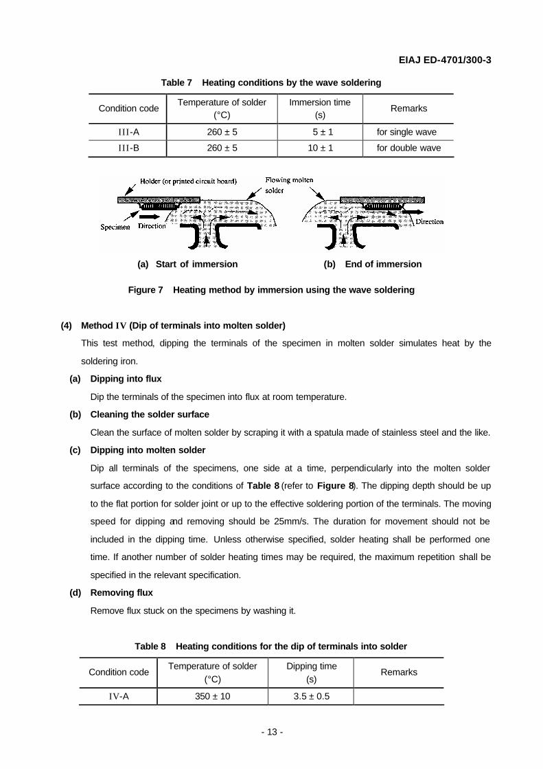
(3) Method III (Wave soldering)
(a) Preparations
Bottom surface of the specimen shall be adhered to the holder by adhesive agent in accordance
with the methods and conditions of the applying adhesive specified in the relevant specification.
Unless otherwise specified in the relevant specification, flux shall not be applied to the holder and
the specimen. (10)
Note (10): Inhibiting the latent heat of evaporation of the flux from rising the temperature of the
specimen, the flux should not be applied to the body of the specimen even if applying
the flux to the specimen is specified in the relevant specification. If applying the flux to
terminals of the specimen, the amount of the flux should be a minimum.
(b) Preheat
The specimen adhered to the holder shall be heated to temperature between 80°C and 140°C for
30s to 60s in the wave soldering apparatus.
(c) Solder heating
After the preheat, the holder with the specimen shall be immersed into flowing molten solder as
shown in Figure 7(a), (b). The immersion conditions shall be selected from Table 7, according to
the real soldering process and conditions. The definition of the immersion time is from the part of
the specimen starting immersion, as shown in Figure 7(a), until the part of the specimen emerging
from molten solder, as shown in Figure 7(b). The package moving time to complete immersion into
the molten solder or complete emergence from the molten solder shall be less than 2s. Unless
otherwise specified, solder heating shall be performed one time. If another number of solder
heating times may be required, the maximum repetition shall be specified in the relevant
specification.
+10 - 0
EIAJ ED-4701/300-3
- 13 -
Table 7 Heating conditions by the wave soldering
Condition code Temperature of solder
(°C) Immersion time
(s) Remarks
III-A 260 ± 5 05 ± 1 for single wave
III-B 260 ± 5 10 ± 1 for double wave
Figure 7 Heating method by immersion using the wave soldering
(4) Method IV (Dip of terminals into molten solder)
This test method, dipping the terminals of the specimen in molten solder simulates heat by the
soldering iron.
(a) Dipping into flux
Dip the terminals of the specimen into flux at room temperature.
(b) Cleaning the solder surface
Clean the surface of molten solder by scraping it with a spatula made of stainless steel and the like.
(c) Dipping into molten solder
Dip all terminals of the specimens, one side at a time, perpendicularly into the molten solder
surface according to the conditions of Table 8 (refer to Figure 8). The dipping depth should be up
to the flat portion for solder joint or up to the effective soldering portion of the terminals. The moving
speed for dipping and removing should be 25mm/s. The duration for movement should not be
included in the dipping time. Unless otherwise specified, solder heating shall be performed one
time. If another number of solder heating times may be required, the maximum repetition shall be
specified in the relevant specification.
(d) Removing flux
Remove flux stuck on the specimens by washing it.
Table 8 Heating conditions for the dip of terminals into solder
Condition code Temperature of solder
(°C) Dipping time
(s) Remarks
IV-A 350 ± 10 3.5 ± 0.5
(a) Start of immersion (b) End of immersion

EIAJ ED-4701/300-3
- 14 -
Figure 8 Method of the dip of terminals into solder
4.5 Recovery
If recovery is specified in the relevant specification, the specimen shall be stored under standard
atmospheric conditions for the time given in the specification, after finishing the solder heating.
4.6 Final measurements
The specimen shall be judged by the results of electrical measurements, visual inspection of external
cracks by 40X optical microscope, and internal cracks and/or delaminations by SAT according to the
PASS/FAIL flow chart shown in Figure 9. The internal delaminations which come under Sub-clause 4.6.3
shall be judged by the results of the reliability test. A special package which can not apply to these test
methods shall be judged by the relevant specification.
4.6.1 Electrical characteristic and visual inspection
A device is considered as a failure if it comes under any of the following:
(1) Electrical failure
(2) External cracks visible under 40X optical microscope
(3) Expansion and/or distortion of the package shape under visual inspection
Remark 3: In the case that expansion and/or distortion of the package shape may cause assembly
problems, it should be considered as a failure.
4.6.2 Inspection 1 by SAT
A specimen is considered as a failure if it comes under any of the following. If internal cracks are
suspected based on SAT, polished cross sections shall be made to verify the suspected site.
(1) Internal cracks that intersect a bond wire, ball bond, or wedge bond
(2) Internal cracks extending from any internal feature to any other internal feature (lead finger, chip, die
attach paddle)
(3) Internal cracks extending more than two-thirds (2/3) the distance from any internal feature to the
outside of the package
4.6.3 Inspection 2 by SAT
A specimen is considered as good if it does not come under Sub-clause 4.6.2 and any of the following: A
specimen shall be judged by the results of reliability test if it exhibits any of follows, except for
delaminations on the back side of the die paddle or die (lead on chip etc.).

EIAJ ED-4701/300-3
- 15 -
(1) Delaminations between the surface of die and the mold
(2) Delaminations of any other internal feature
(3) Internal cracks which do not come under Sub-clause 4.6.2
4.6.4 Reliability test
The specimen shall be judged by the results of reliability test if it comes under item 4.6.3.
Reliability test method referred to shall be Moisture soaking and soldering heat stress series test
(ED-4701/100 TEST METHOD 104) and specified the relevant specification.
Figure 9 PASS/FAIL flow chart

EIAJ ED-4701/300-3
- 16 -
5. Storage limit from opening dry pack to soldering
The storage limit from opening dry pack to soldering classifies on 10 ranks. Baking before soldering is
necessary if SMDs stores over the storage limit.
In case of baking performed before dry packing, the floor life should be included the time from end of
baking to dry packing, and baking before dry packing must perform both of SMD and a tray.
When rank S is used, moisture soaking condition, storage condition after unpacking and storage limit after
unpacking should be specified in the relevant specification.
Table 9 Rank of resistance to soldering heat
Rank Moisture soaking condition * the second stage moisture soaking
Storage condition after unpacking
Storage limit after unpacking
A * 85°C, 85%RH, 168h3 ≤ 30°C, 85%RH Unlimited
B * 85°C, 65%RH, 168h ≤ 30°C, 70%RH 1 year
C * 30°C, 70%RH, 672h (11) ≤ 30°C, 70%RH 4 weeks
D * 30°C, 70%RH, 336h (11) ≤ 30°C, 70%RH 2 weeks
E * 30°C, 70%RH, 168h (11) ≤ 30°C, 70%RH 168h
F * 30°C, 70%RH, 96h (11) ≤ 30°C, 70%RH 96h
G * 30°C, 70%RH, 72h (11) ≤ 30°C, 70%RH 72h
H * 30°C, 70%RH, 48h (11) ≤ 30°C, 70%RH 48h
I * 30°C, 70%RH, 24h (11) ≤ 30°C, 70%RH 24h
S * specified individually specified individually specified individually
Note (11): Acceleration soaking such as 85°C, 65%RH may be used if moisture density under
acceleration soaking condition is confirmed over the moisture density under 30°C,
70%RH condition. The simulation results may be used for confirmation.

EIAJ ED-4701/300-3
- 17 -
6. Information to be given in the relevant specification
(1) Holder (When it is different from the specified ones) [Sub-clause 2.7]
(2) Composition of the solder (When it is different from the specified ones) [Sub-clause 3.2]
(3) Mixing ratio of flux (When it is different from the specified ones) [Sub-clause 3.3]
(4) Items and conditions of the initial measurements [Sub-clause 4.1]
(5) Baking (When required) [Sub-clause 4.2]
(6) Moisture soaking conditions (When it is different from the specified ones) [Sub-clause 4.3]
(7) Time period between the moisture soaking and the solder heating
(When it is different from the specified ones) [Sub-clause 4.3]
(8) Allowable maximum conditions (temperature and relative humidity)
in the dry pack and the first stage moisture soaking conditions corresponded
to their conditions [Sub-clause 4.3(1)]
(9) Storage conditions of SMDs after opening the dry pack and the second stage
moisture soaking conditions corresponded to their conditions [Sub-clause 4.3(1)]
(10) Selection of moisture soaking conditions for non-dry packed SMD [Sub-clause 4.3(2)]
(11) Moisture soaking time of condition A for non-dry packed SMD [Sub-clause 4.3(2)]
(12) Moisture soaking time when moisture absorption is saturated less than 168h [Sub-clause 4.3(2)]
(13) Baking treatment conditions instead of the moisture soaking
(When it is necessary) [Sub-clause 4.3]
(14) Number of times of solder heating
(When it is different from the specified ones) [Sub-clause 4.4]
(15) Moisture soaking conditions between the solder heatings
(When it is necessary) [Sub-clause 4.4]
(16) Selection of solder heating method and conditions,
or another conditions different from Table 3 [Sub-clause 4.4]
(17) Adhesion method of specimen [Sub-clause 4.4(3)]
(18) Application conditions of flux (When it is necessary) [Sub-clause 4.4(3)]
(19) Time of the recovery (When it is necessary) [Sub-clause 4.5]
(20) Items and conditions of the final measurements [Sub-clause 4.6]
(21) Moisture soaking condition, storage condition after unpacking
and storage limit after unpacking if rank S used [Sub-clause 5.]

EIAJ ED-4701/300-3
- 18 -
REFERENCE
1. Purpose of establishment
At the beginning, SMDs (surface mounting devices) used to be soldered on the printed circuit board by
hand work using soldering iron. At that time SMD did not present any problem in particular related to
thermal stress during soldering. Since 1980’s, SMD began to attract the attention in view of its advantages
related to high density mounting, and such methods as vapor phase reflow soldering, infrared reflow
soldering, convection reflow soldering and wave soldering, etc., that heating the whole component part
and surface of the printed circuit board (overall heating method) become widespread in view of their merits
related to batch soldering of the component parts.
However, in these methods, not only the terminals but also the body of the SMD are heated up to
temperatures above the melting point of the solder, and it was found that package crack may occur in the
case of plastic encapsulated SMD. When SMDs absorbing moisture during room storage are soldered, the
package crack may be occurred by the high pressure water vapor generated internally due to the heat of
the package during soldering. This problem tends to occur more frequently in IC and LSI containing large-
sized dice, and is very rare in discrete semiconductors.
Then this test method was established by examining the problem of moisture absorption of SMDs during
the storage and the conditions of the soldering.
2. Evolution of establishment
Since SMD for ICs and LSIs are more susceptible to soldering heat compared with other surface mounting
components such as passive components, and they are more influenced by the effects of moisture
absorption during storage before soldering, the provisional standards EIAJ EDX-4701 (Test Methods for
Resistance to soldering heat of surface mounting devices for integrated circuits) were established on
march, 1990. After that, the test method A-133 in EIAJ ED-4701 was established properly on February,
1992 by making partial modifications in EIAJ EDX-4701, so as to expand the scope of application to
hermetic sealed SMD and discrete semiconductors.
And then, the test method A-133A was established on March, 1995 by revising the test method A-133, so
as to correspond to the problem of storage after opening the dry pack and the problems which were found
in infrared reflow soldering and wave soldering. And further, the test method A-133B was established on
June, 1998 by revising the test method A-133A, so as to correspond to the problem of moisture absorption
between plural times of soldering, classification of solder heating by the infrared reflow soldering and the
convection reflow soldering depending on the package volume of SMD, and internal inspection method
using by the scanning acoustic tomography (SAT).
In addition, the rank of resistance to soldering heat were added with consideration of JEDEC level and
acceleration moisture soaking and revised as A-133C on October, 2000.
A classification reflow profiles for SMD mounted by Pb free solder paste were added to correspond to Pb
free soldering, and revised as EIAJ ED-4701/300 TEST METHOD 301A on June, 2002.
Furthermore, solder heating times and reflow profiles for SMD mounted by Pb free solder paste were
reviewed and revised on April, 2005.

EIAJ ED-4701/300-3
- 19 -
3. Presetting the temperature conditions of the solder heating equipment
3.1 Presetting the temperature conditions of the reflow soldering method
Damages occurring in the SMDs during the soldering depend on the packaged body temperature and the
moisture concentration at the first interface in package. (It will be explained in detail later on.) In the
infrared reflow soldering, convection reflow soldering and vapor phase reflow soldering, when heating
conditions are preset by observing temperature of SMD terminals or atmosphere in these equipment,
serious doubts about the repeatability of the test results occur because there are substantial differences of
the packaged body temperature depending on such factors as the combination of temperature presetting
conditions of the heating equipment and the speed conditions of the belt conveyor, types of the heating
equipment, the type of the SMD, and material and size of the holder. Therefore, it is indispensable to
specify the heating conditions in the reflow soldering method in terms of the temperature of the SMD body,
(temperature of the top surface of the SMD) and the repeatability of the test results must be secured.
The solder heating conditions must be preset by measuring temperature of the top surface of the SMD that
a thermocouple attached to its surface as shown in Figure 1, in the heating equipment according to the
same steps of procedure as those ones of the test. A thermocouple must be attached to the SMD surface
tightly with the adhesive agent or the thin heat proof tape. As long as the conditions are specified in terms
of the surface temperature of the SMD, it is not necessary to specify the model of the heating equipment
and to specified details of the holder.
Moreover, a thermocouple was attached to the top surface of the SMD by the adhesive agent in test
method A-133 and A-133A, however, the method of attaching a thermocouple to the package surface with
the thin heat proof tape was added to the test method A-133B, because to be able to measure the
temperature sufficiently with the thin heat proof tape was ascertained.
3.2 Presetting the temperature conditions of the wave soldering
The heating conditions related to the wave soldering are specified in terms of the molten solder
temperature and dipping duration, because a quantity of heat conducted and conveyed from the molten
solder to SMD is stable. However, the temperature conditions of preheat must be specified in terms of the
surface temperature of the SMD.
4. Test procedure
4.1 Baking
When saturated moisture soaking conditions are assumed as a premise, the baking is not needed.
However, since moisture soaking conditions specified in Sub-clause 4.3 are set for the almost saturated
conditions, are not set for the perfect saturated conditions, and the test results may depend on whether the
baking is performed or not. Therefore the baking is needed to heighten reproducibility of the tests.

EIAJ ED-4701/300-3
- 20 -
4.2 Moisture soaking
It was found that package cracks during solder heating were induced by pressure of water vapor from the
moisture contained in the resin near the bottom surface of die pad or near top surface of the die
(hereinafter called the first interface). Such being the case, moisture soaking conditions must be specified
in such a way that the moisture concentration at the first interface coincides with the moisture
concentration after the actual storage of SMDs. Therefore moisture soaking conditions specified in Sub-
clause 4.3 are specified in such a way that the moisture concentration at the first interface coincides with
the moisture concentration of the allowable maximum storage conditions. Details related moisture soaking
are explained below.
4.2.1 Method to obtain the moisture concentration of the resin at the first interface
Since the moisture concentration at the first interface can not be measured, the moisture absorption
characteristics of the resin are analyzed by the fitting technique shown below, and the moisture
concentration can be calculated from the numerical values of these characteristics.
In the first place, when a resin plate (having side areas as small as possible) with thickness d cm is stored
under constant temperature and constant humidity conditions, moisture penetrates from the surface to the
interior of the resin plate according to the diffusion law of Fick, given by the equation (1).
x
txCDt
txC∂
∂=∂
∂ ),(),( 2
························································································ (1)
where C(x, t): Moisture concentration (mg/cm3) at the point x (cm) of the thickness coordinate having its
origin at the center of the resin plate, and at the time t (s)
where D(x, t): Moisture diffusion coefficient (cm2/s) of the resin
Assuming that immediately after the storage the surface of the resin reaches the saturated moisture
concentration Qs, the boundary conditions are given by the following equation.
C(x, t)=0 )0,22
( =<<− td
xd
······································································· (2)
C(x, t)=Qs )0,2
( >±= td
x
and the equation (3) is obtained as a result.
+
+−
−= ∑∞
=
+−
0
)12( 12cos
12)1(4
1),( 2
22
n
dDtnn
xd
ne
nQstxC π
π
π
·································· (3)
On the other hand, given that area of the resin plate is S, amount of the moisture quantity W (t) (g) of the
resin plate will be given by equation (4).
∫ ∑−
∞
=
+−
+−⋅⋅== 2
2 0
)12(
22
2
22
)12(8
1),()(d
dn
dDtn
en
QsdSdxtxCStWπ
π ···················· (4)

EIAJ ED-4701/300-3
- 21 -
Given Bolzmann factor k, absolute temperature T, pressure of moisture P, activation energy of moisture
diffusion Ed, activation energy of moisture dissolubility Es, coefficient D0, n and S0, the moisture diffusion
coefficient D and the saturated moisture concentration Qs can be obtained by equations (5) and (6).
kTEd
eDD−
= 0 ········································································································· (5)
kT
Esn eSPQs 0= ····································································································· (6)
By comparing equation (4) and the values of measured amount of the moisture quantity that the resin plate
is stored under constant temperature and constant humidity conditions, Es, Ed, D0, S0 and n which are the
moisture soaking parameters can be obtain by fitting technique. These moisture soaking parameters
depend on the kind of resin. When these quantities are obtained, the moisture concentration at various
places inside the resin can be obtained by equation (3). The moisture concentration at bottom surface of
the die pad and top surface of the chip surface (first interface) can be obtained by substituting x=0 in the
equation (the cos term becomes 1).
4.2.2 Characteristics of saturated moisture concentration of resin
The moisture concentration of resin at the saturation depends on the relative humidity clearly as shown in
Figure B1. Although Figure B1 is one of example, another type of resin has similar characteristics, too.
So the condition of moisture soaking to be fit for the assumed storage environment can be obtained from
Figure B1.
Figure B1 Examples of dependence, on
temperature and relative humidity, of the saturated moisture concentration of the resin
Figure B2 Example of moisture soaking
speed depended on temperature (Speed at 30°C=1)

EIAJ ED-4701/300-3
- 22 -
4.2.3 Moisture absorption speed
The moisture absorption speed in the resin is directly proportional to moisture diffusion coefficient D
depended on temperature, therefore, the absorption speed increase according to temperature. When
rising temperature from 30°C to 85°C, the absorption speed can be accelerated roughly to one figure as
shown in Figure B2. By defining the resin thickness (length between surface of SMD to the first interface)
as shown in Figure B3, the absorption speed at the first interface is inversely proportional to the square of
the resin thickness (d/2 in the equation (3) corresponds to the resin thickness). Therefore the longer
moisture soaking time is needed in order to saturate the moisture absorption of thicker SMDs. (refer to
Figure B4)
Figure B3 Definition of resin thickness
Figure B4 Example of dependence, on the resin
thickness, of moisture soaking time at 85°C to reach moisture saturation
4.2.4 Necessity of saturated conditions of moisture soaking
Moisture sensitive SMDs can be stored for long term in the dry pack, and absorb moisture toward moisture
saturation under conditions in the dry pack that atmosphere in the dry pack stored for long time is
stabilized to lower humidity. The moisture concentration absorbed in the dry pack will be higher than that
between opening the dry pack and the soldering when SMDs have medium and thicker thickness.
Therefore, the first step moisture soaking corresponded to storage condition in the dry pack specified in
Sub-clause 4.3(1) must simulate the above moisture saturation.
Moisture absorption of the non dry packed SMDs which is stored in the room is unstable, and does over
again to absorb and dry. The non dry packed SMDs must be fit for long term storage under the worst
condition of the average humidity in the storage atmosphere. So the moisture soaking which corresponds
to the saturated moisture absorption of the worst condition is required.

EIAJ ED-4701/300-3
- 23 -
4.2.5 Moisture soaking conditions for the dry packed SMDs and rank of resistance to soldering heat
Dry packed SMD absorbed moisture not only after unpacking but also in a dry pack. Moisture absorption in
a dry pack is negligible when baking performed before dry packing, however humidity control is necessary
from end of baking to dry packing. These absorption stages should be considered when absorption
condition decides.
The manufacturer controls the moisture concentration of SMD before packing, and then, seal up SMD in
the dry pack composed of a moisture proof bag and desiccants. But the dry pack is not perfect (the relative
humidity in the dry pack is not 0%RH). SMDs, IC-trays, desiccants, etc. that are packed in the dry pack
contain the moisture a little before the packing. The relative humidity in the dry pack differs in whether the
baking of SMDs and IC-trays is performed before packing, how do the humidity control, how to treat the
contents. However the moisture control is performed, there are the pinhole and the damage of the bag, the
unsealing and resealing a bag in the shipping.
Generally the humidity indicator is enclosed in the dry pack. This indicator is an exclusive type or the blue
beads to be mixed with the desiccant. Generally the sensitivity of the humidity indicator which the
Japanese semiconductor manufacturer uses is about 30%RH, and it is requested user to confirm that the
humidity in the dry pack is less than 30%RH just after opening the dry pack.
And generally, for the dry pack, it is permitted to store a long term with SMD in the cabinet which is
controlled in less than 30%RH.
Besides, it can be considered that the moisture amount, which is absorbed in SMD during such operation
for a short time as inspection or repacking of SMDs, can be recovered to the original condition if SMDs are
sealed up in the dry pack or kept in the cabinet, which is controlled in less than 30%RH, after that
operation.
As mentioned above, conditions of the first stage moisture soaking is 85°C, 30%RH, 168h (but, it should
be saturated.) from Figure B1 if the conditions of humidity in the dry pack or storage is controlled by
30%RH. However, Table 1 is shown as a typical example as some of semiconductor suppliers specify
other conditions from 30%RH. (In USA, EIA/JEP 113-B specifies 10%RH for example.) The strict control,
such as monitor of the weight gain of SMDs in the dry pack, will not be required, if the first stage moisture
soaking conditions are set at the worst condition of humidity in the dry pack. On the other hand, the first
stage moisture soaking condition less than 30%RH to be saturated can be applied when the humidity in
the dry pack is controlled strictly. (For example, the specimen may be soaked by 85°C, 10%RH if it is
controlled below 10%RH.) In this case, several limited conditions, such as execution of the weight gain
monitoring of SMDs in the dry pack, or prohibition of opening and resealing of the dry pack, may be often
required.

EIAJ ED-4701/300-3
- 24 -
The maximum allowable storage conditions of SMDs between opening the dry pack and soldering are
different by the types of SMDs, which will be specified by semiconductor suppliers. So, conditions of the
second stage moisture soaking should be specified in the relevant specification. Conditions of 30°C,
70%RH, 168h are used as the maximum allowable storage conditions of SMDs in Japan by many
Japanese semiconductor suppliers. Accordingly, these conditions are shown in Table 1 as the
representative condition. (In Japan, 30°C of temperature is standardized, however, various conditions for
humidity (60%RH to 85%RH) and soaking time (few hours to 336 hours) are applied).
The Figure B5 shows comparison of the moisture calculation results between maximum allowable storage
conditions and moisture soaking conditions shown in Table 1. Moisture absorption of all kinds of SMDs will
be saturated not related with the resin thickness when SMDs are stored for a long term (1 year for
example) in the dry pack. It is understood that the soaking condition of 85°C, 30%RH to be saturated (the
first stage moisture soaking) can be applied. Besides, the soaking conditions of 30°C, 70%RH for 168h
after the first stage moisture soaking can be applied to the case of that SMDs are stored under conditions
of 30°C, 70%RH for 168h after the storage in the dry pack for a long term. Then, the soaking conditions of
two steps are required independent of the kinds of SMDs due to correspond to the real storage conditions
of SMDs.
The rank of resistance to soldering heat is laid down. The rank is included JEDEC’s level. A comparison
between JEDEC’s level and JEITA’s rank is shown in Table B1.
The storage condition assumed 30°C, 60%RH in JEDEC’s standard, and 30°C, 70%RH in JEITA’s. So the
classification of resistance to soldering heat in JEITA’s is named “rank” and they have distinguished
between JEDEC’s level and JEITA’s rank. Furthermore, lead free soldering is also considered when the
rank is fixed.
Figure B5 Comparison between moisture soaking conditions
Figure B5 and assumed storage conditions for dry packed SMDs

EIAJ ED-4701/300-3
- 25 -
Table B1 Comparison between JEITA’s rank and JEDEC’s level
JEITA (EIAJ ED-4701/301B) JEDEC(IPC/JEDEC J-STD-020C)
Rank Storage conditions Storage time Level Storage conditions Storage time
A ≤ 30°C, 85%RH Unlimited 1 ≤ 30°C, 85%RH Unlimited
B ≤ 30°C, 70%RH 1 year 2 ≤ 30°C, 60%RH 1 year
C ≤ 30°C, 70%RH 4 weeks 2a ≤ 30°C, 60%RH 4 weeks
D ≤ 30°C, 70%RH 2 weeks – – –
E ≤ 30°C, 70%RH 168h 3 ≤ 30°C, 60%RH 168h
F ≤ 30°C, 70%RH 96h – – –
G ≤ 30°C, 70%RH 72h 4 ≤ 30°C, 60%RH 72h
H ≤ 30°C, 70%RH 48h 5 ≤ 30°C, 60%RH 48h
I ≤ 30°C, 70%RH 24h 5a ≤ 30°C, 60%RH 24h
S specified individually
specified individually
6 ≤ 30°C, 60%RH TOL(1)
Note (1): TOL: Time On Label
Accelerated moisture soaking condition is studied since the test time of the two step moisture soaking is
long. The one step moisture soaking can be substituted for the two step moisture soaking, if the moisture
density under the one step moisture soaking is more than the density of the two step moisture soaking.
The second step of the moisture soaking can be also accelerated moisture soaking. And a simulation
result of moisture soaking is acceptable. In the case of rank E, the condition of the second step moisture
soaking can be 85°C, 65%RH, 19h, and 85°C, 65%RH 38h for 1 time is also acceptable as shown in
Figure B6. However the condition depend on the package type and a material of resin. Acceleration
condition varies and the major conditions are as follows.
85°C, 65%RH
85°C, 85%RH
85°C, 70%RH
The temperature of acceleration condition does not exceed the glass transition temperature of a resin.
MET (Manufacturer Exposure Time) is not stated in this standard, because it makes the procedure
complicated. The worst temperature and humidity condition in a dry pack is stated as an alternative plan.

EIAJ ED-4701/300-3
- 26 -
Figure B6 Example of accelerated moisture soaking conditions
4.2.6 Soaking conditions for non-dry packed SMDs
The moisture soaking conditions of 85°C, 65%RH to saturation is required for 30°C, 70%RH, which is the
average value for several months (around five months) during summer season in Japan if SMDs are kept
in a room such as store house. (Refer to Figure B1.) Generally 168h of soaking time is needed or 336h of
soaking time is needed for thicker SMDs, which must be specified in the relevant specification.
However, the overseas environmental conditions should be considered because the case that electronic
equipment is assembled at a foreign plant has increased recently. The average environmental conditions
of 30°C, 85%RH will be enough for these cases, when SMDs are stored in a room. The conditions of 85°C,
85%RH, which is used for temperature humidity test generally, can be applied as the soaking conditions
for this case. Figure B1 shows that the soaking conditions of 85°C, 85%RH is corresponded to the
storage conditions of 30°C, 90%RH. So, the conditions of 85°C, 85%RH for 168h, not to saturation, can be
applied for almost of SMDs. (Refer to Figure B7.) The soaking conditions must be specified in relevant
specification if a long soaking time is necessary for thick SMDs.

EIAJ ED-4701/300-3
- 27 -
Figure B7 Example of comparison between storage of 30°C, 85%RH for 1 year and moisture soaking of 85°C, 85%RH
4.2.7 Case of that moisture soaking is not required
Moisture soaking is not required for hermetic packaged SMDs because moisture is not absorbed in them.
And, in accordance with the relevant specification the moisture soaking can be omitted for plastic molded
SMDs having a small die because moisture can not affect them.
Figure B8 Comparison between single stage moisture soaking
and assumed storage condition

EIAJ ED-4701/300-3
- 28 -
4.2.8 Other soaking conditions
Other conditions, 85°C, 85%RH for a short time, such as 30h or 75h, etc., were proposed during
establishment of EIAJ EDX-4701. In these unsaturated conditions, thin SMDs are soaked excessively and
thick SMDs are soaked insufficiently as shown in Figure B8 because the first stage moisture soaking is
omitted. The moisture concentration at the first interface after moisture soaking become lower than that
after real storage if SMDs are thicker. Accordingly, these conditions had not been adopted.
4.2.9 Moisture soaking condition in USA
In USA, moisture soaking conditions and storage conditions (Floor life) were specified in standards of
JEDEC-IPC/J-STD-020C, J-STD-033A and EIA/JEP 113-B. Difference points of moisture soaking
conditions and storage conditions between JEITA and JEDEC are shown in Table B2.
Table B2 Difference points of moisture soaking conditions and storage conditions
between JEITA and JEDEC
Moisture absorption in manufacture’s line
Moisture absorption in dry pack
Moisture absorption in assembly line
JEITA (EIAJ ED-4701/301B)
Not specified 85°C/30%RH/168h 30°C/70%RH
Floor life
JEDEC (IPC/JEDEC J-STD-020C)
30°C/60%RH/24h Not specified 30°C/60%RH
Floor life
There are big difference points of moisture soaking conditions and storage conditions between JEITA and
JEDEC. In JEDEC standard, no moisture absorption is assumed in the dry pack (the allowable upper limit
of relative humidity in the dry pack is 10%), on the other hand, moisture absorption in the dry pack is
assumed in JEITA standard. Baking process before dry packing is required in JEDEC standard. And then,
moisture soaking conditions and storage conditions in the above standards were classified into 6 levels as
follows.
(1) LEVEL-1 and LEVEL-2
LEVEl-1 of moisture soaking conditions requires 85°C, 85%RH, 168h for long term (limit free) storage
at 30°C, 85%RH. And LEVEL-2 of moisture soaking conditions requires 85°C, 60%RH, 168h for long
term (1 year) storage at 30°C, 60%RH. LEVEL-1 is almost corresponds with Condition B given in
Table 2 of Sub-clause 4.3. But as Figure B7 shows, there is a case that some SMDs are short of
moisture soaking time for long term storage at 30°C, 85%.

EIAJ ED-4701/300-3
- 29 -
(2) LEVEL-2a to LEVEL-5
LEVELs 2a to 5 stipulate moisture soaking conditions to cover storage time at 30°C, 60%RH after
opening the dry pack (it is defined as floor life and is classified into five parts of storage time). These
levels require 24h for Manufacture’s Exposure Time (MET) between bake and bag plus the maximum
time allowed out of the bag at the distributor’s facility. LEVEL-3 is for SMDs to solder by 168h after
opening the dry pack ( it is mean that floor life is 168h) and moisture soaking condition is 30°C,
60%RH, 192h (floor life plus MET(=24h)) after baking of 125°C, 24h. LEVEL-4 requires moisture
soaking time of 96h for floor life of 72h and LEVEL-5 requires soaking time of 48h or 72h for floor life
of 24h or 48h, in the same way as LEVEL-3.
As stated above, these moisture soaking conditions are based on conditions that relative humidity in
the dry pack is 0%RH because these consist of the baking, the MET and the floor life. Therefor SMDs,
IC trays and other materials in dry pack must be completely baked just before packing into the dry
pack by semiconductor suppliers.
On the other hand, in JEDEC-IPC/J-STD-020C, J-STD-033A and EIA/JEP 113-B, their permissible
relative humidity in the dry pack was 10%RH, and further, it was specified that SMDs can be stored
for long a time (limit free) after opening the dry pack when relative humidity is below 10%RH.
Therefore LEVEL-2a to 5 did not correspond with the conditions of JEDEC-IPC/J-STD-020C,
J-STD-033A and EIA/JEP 113-B.
Figure B9 shows comparison of moisture soaking conditions of LEVEL-3 and storage conditions
(A: 0%RH in the dry pack, B: 10%RH in the dry pack). This figure shows the following. If SMDs are
stored in the perfectly dried dry pack for long a time (assumption: MET=0), moisture soaking
condition of LEVEL-3 can cover floor life of 30°C, 60%RH, 168h after opening the perfectly dried dry
pack. But when relative humidity in the dry pack become 10%RH, moisture soaking condition of
LEVEL-3 can not cover the floor life of 30°C, 60%RH, 168h. In addition, it can not cover the floor life
of thick package that relative humidity in dry pack becomes 10%RH.
As stated above, moisture soaking conditions of LEVEL 2a to 5 were based on ideal conditions
that the contents in dry pack were dried completely and can not cover long time storage at
permissible relative humidity 10%RH being stipulated by JEDEC-IPC/J-STD-020C, J-STD-033A
and EIA/JEP 113-B in dry pack.
Therefore moisture soaking conditions of LEVEL 2a to 5 were not adopted at this committee because
these conditions did not fit real assembly environment because they can not guarantee relative
humidity of 0%RH in the dry pack as follows.
(a) We do not have humidity indicator to correctly guarantee 0%RH in the dry pack.
(b) It is very difficult to completely dry and pack all contents in the dry pack.
(c) We do not have system to control packing the dry pack and temporary opening the dry pack in
distributor’s facility.
(d) We can not supply pinhole free or scratch free dry pack.

EIAJ ED-4701/300-3
- 30 -
In addition, moisture soaking conditions of EIAJ can cover one of customer’s requirements that SMDs
are stored in dry cabinet controlled humidity (below 30%RH) instead of dry pack. On the other hand,
the upper relative humidity limit in a dry pack was changed to 10% and revised as JEDEC-IPC/
J-STD-020C, J-STD-033A and EIA/JEP 113-B following the discussion of JEDEC/JEITA Joint
Meeting. A little lack of moisture soak may result as a thick package with 10% of relative humidity.
However it is conceivable that there is no contradiction in the moisture soak condition when the
strength of a package is considered.
As mentioned above, it is possible to classify the moisture soaking condition by the presence of the
baking before dry packing, and the comparison of condition is shown in Table B3. When baking
performed before dry packing, It is necessary to enclose the humidity indicator card which shows
10%RH or less in the dry pack to guarantee humidity, and to control of time of baking before dry
packing and time to dry packing after baking.
Figure B9 Comparison between moisture soaking conditions and assumed storage conditions for JEDEC Floor Life LEVEL-3
Table B3 Comparison of moisture soaking conditions by the presence of baking
Precondition before dry packing
Moisture absorption in manufacture’s line
Moisture absorption in dry pack
Moisture absorption in assembly line
Baking not performed 85°C/30%RH/168h
(The humidity in the dry pack is 30%RH or less) 30°C/70%RH
Floor life
Baking performed
Moisture absorption in manufacture’s line (Moisture density
depends on time after baking process)
No moisture absorption is assumed
30°C/70%RH Floor life
0 0.5 1 1.5 0
2
4
6
8
レジン厚 mm
A: 防湿包装内保管+30, 60%RH, 168h 保管 (包装内:0%RH) B: 防湿包装内保管+30, 60%RH, 168h 保管 (包装内:10%RH)
LEVEL-3 の加湿条件 (30, 60%RH, 192h)
A B
Soak condition for LEVEL-3 (30°C, 60%RH, 192h)
30°C, 10%RH, 1year
A: Long storage in the dry pack + 30°C, 60%RH, 168h (Relative humidity in the dry pack: 0%RH)
B: Long storage in the dry pack + 30°C, 60%RH, 168h
(Relative humidity in the dry pack: 10%RH)
Resin thickness (mm)

EIAJ ED-4701/300-3
- 31 -
(3) LEVEL-6
This standard specifies that those SMDs which should be soldered within TOL (Time on label) after
baking, shall be stored at 30°C, 60%RH for 6h.
4.2.10 Moisture soaking between plural solder heating
Moisture soaking between plural solder heatings, a new proposal on moisture soaking conditions, as
shown in Figure B10(B) was given during discussion of revising this test method because SMDs absorb
moisture between real plural soldering process and it is practical as shown in Figure B10(A).
Moisture soaking of Sub-clause 4.3(1) is performed as shown in Figure B10(B) that the first stage
moisture soaking corresponding to long storage in the dry pack is performed and subsequently, the
second stage moisture soaking corresponding to the full amount of storage between opening the dry pack
and final soldering is performed. Therefore real storage conditions after opening the dry pack, the full
amount of storage between opening the dry pack and final soldering, must be controlled within conditions
of the second stage moisture soaking.
Our committee members made experimentations that the second stage moisture soaking of this test
method mentioned above and the new proposal as shown in Figure B10(C). And the assumption of these
experimentations is that conditions of the second stage moisture soaking coincide with the sum of soaking
conditions between the first stage moisture soaking and final solder heating of the new proposal.
Consequently, two kind of experimentation results are obtained, on the hand moisture soaking of this test
method is severer than new proposal, on the other hand the new proposal is severer than moisture
soaking of this test method, it is understood that these experimentation results are depended on structure
of the SMDs.
In the new proposal, the second stage moisture soaking must be divided into two conditions, but
semiconductor user have various storage conditions. Therefore the ratio of dividing the second stage
moisture soaking can not be specified.
As mentioned above, our committee have decided that the new proposal, which can be adopted if required
by the relevant specification, is not adopted.

EIAJ ED-4701/300-3
- 32 -
Figure B10 Examples of real storage conditions and moisture soaking conditions in the event that twice soldering are performed
4.3 Solder heating
4.3.1 Plural solder heating
Number of times of the solder heating of this test method is three times, because real soldering process
has possibility of three times of soldering. Therefore three times of the solder heating can be applicable as
the maximum times when it is specified into the relevant specification. In this case, if soldering temperature
during rework is lower (temperature of SMD’s body is below 200°C, or heating by the soldering iron),
adding its number of times to that of the solder heating may be not needed.
The moisture soaking of this test method corresponds to the moisture soaking from opening the dry pack
to the final soldering of the real soldering process. Therefore, moisture soaking is not carried out between
plural solder heatings (see Sub-clause 4.2.10).
When the solder heating is carried out twice or more, the heating procedures specified in Sub-clause 4.4
must be repeated. For example, when solder heating of Method II at 215°C for 40s is repeated twice,
heating of 215°C for 40s is made, subsequently, temperature must be cooled down to below 50°C, and
temperature must be raised by the same conditions again. Substitute conditions such as 215°C for 80s are
not appropriate though duration time is equal to twice of 40s.
(A) Example of real storage procedure and conditions
(B) Moisture soaking procedure and conditions of this test method
(C) Example of proposal of moisture soaking procedure conditions

EIAJ ED-4701/300-3
- 33 -
4.3.2 Temperature profile method I (Infrared reflow, Convection reflow soldering)
Since the purpose of soldering is to connect SMDs to the printed circuit board, measuring temperature of
the terminals of SMDs is an ideal for the soldering heat test. However, SMD’s resistance to soldering heat
depends on the surface temperature of the body. If conditions of the solder heating are defined by
temperature of the terminals, test results will be unstable as mentioned in Sub-clause 3.1. Therefore, in
order to ensure test repeatability, conditions of the solder heating for reflow methods could not be help
defining temperature of the body surface. Further, as temperature profile of these methods are unstable,
temperature of SMD’s body surface must be measured for each time of soldering heat test.
The maximum temperature at the body surface during solder heating depends on heat capacity, heat
resistance of SMDs. Therefore each members of this committee conducted experiments in correlation
between surface temperature at the time of soldering, and body thickness and volume using various SMDs,
which indicated a good correlation between volume of SMDs and body surface temperature. With
considering circumstance mentioned above, it is decided that the heating condition I-I-A (peak
temperature: from 235°C to 240°C) shown in Table 3 is applied to small of medium size SMDs whose
volume is less than 2,000mm3, and the heating condition I-I-B (peak temperature: from 220°C to 225°C) is
applied to large size SMDs whose volume is over 2,000mm3.
For getting good solder junction, SMD terminals should be heated up to at least 210°C (Sn-Pb solder
paste). When various SMDs having differ in volume are soldered on the same printed circuit board, the
larger the device volume is, the lower its peak temperature of terminals becomes. Therefore, soldering
conditions must be set in terms of the terminal temperature of the largest SMD at least 210°C.
When terminal temperature of the largest SMD is set from 210°C to 215°C, body surface of larger SMDs
having over 2,000mm3 in volume on the same printed circuit board do not reach 220°C, and that of small
SMDs having less than 2,000mm3 on the same printed circuit board reach over 220°C. Therefore applying
solder heating conditions are decided as mentioned above.
This test method had adopted solder heating condition I-I-A. In this case, if this condition is applied to
large SMDs, temperature of the printed circuit board reaches from 250°C to 280°C and foul smell is
generated from heated printed circuit board, because power of reflow furnace must be increased in order
to heat large SMDs having tendency that raise speed of temperature is slower. Therefore condition I-I-B
was added to this test method as a corrective action against this problem, and can be selected one of two
conditions.
To examine the Pb free soldering conditions, each members of this committee conducted experiments in
correlation between surface temperature at the time of soldering, and body thickness and volume using
various SMDs, which indicated a good correlation between volume of SMDs and body surface temperature.
With considering circumstance mentioned above, the peak temperature conditions with 3 levels were
decided according to the matrix of package thickness and/or volume. An end point of 350 mm3 was added
in package volume to correspond to temperature rise of 20°C due to an introduction of Pb free soldering.
Moreover, this value of 350 mm3 is adopted in the JEDEC specification. Temperature range was
introduced to peak temperature to clear the peak temperature definition.

EIAJ ED-4701/300-3
- 34 -
In the case of lead type package such as QFP, there is no problem of solderability that the temperature
profile is specified in terms of the temperature of top surface of the specimen because the temperature of
lead terminal of the specimen is higher than top surface. However, in the case of BGA, the temperature of
lead terminal tends to lower than top surface. Therefore the peak temperature of top surface of the
specimen was specified at most severe condition of 260°C not according to the package thickness and
volume in EIAJ ED-4701/300 TEST METHOD 301A. However, the peak temperature was reviewed for this
standard revision and temperature profile is not distinguished between QFP and BGA in JEDEC standard.
Therefore committee discussed whether the classification of package thickness and volume of peak
temperature is applicable in BGA. As a result, the classification of Table 4 is adopted in condition B of
Table 5.
4.3.3 Temperature profile of method II (Vapor Phase Reflow)
Because that the upper temperature limit, which is the property of perfluorocarbon, reaches 215±5°C, the
period while the upper temperature limit is to be kept should be longer, and IEC-749 second edition
adopted the period of 40s, the period is decided to 40s.
4.3.4 Method III (Wave soldering)
A test method that the entire of the specimen are immerse into molten solder as shown in Figure B11 was
specified in EIAJ EDX-4701 and EIAJ ED-4701, IEC-749 second edition.
Figure B11 Whole immersion method into molten solder
However, it is reported that the conventional method shown in Figure B11 becomes too severe as a test
method, because the entire body of SMD is immersed in the molten solder and the temperature of SMD
itself goes up to higher degrees than that of actual soldering. Meanwhile, when the wave soldering method
is used, the temperature of the inside of the package goes up slowly because only one side of SMD is
immersed into the flowing molten solder, and the radiation effect from the other side of SMD is also
recognized. Consequently, the peak temperature of the inside of the SMDs is lower than that during
immersing entire of SMDs into solder bath.

EIAJ ED-4701/300-3
- 35 -
Accordingly, the conventional method was abolished when the test method A-133 was revised, and the
new method, immersion into the flowing molten solder after the SMD is temporarily fixed on the holder as
shown in Figure 7, was introduced in order to match the actual soldering condition.
The heating conditions were decided as Condition III-A (260°C, 5s) and III-B (260°C, 10s),
corresponding to the single-wave and the double-wave soldering.
If flux is applied to the specimen, the flux vaporizes quickly during the immersion. At this time, the latent
heat is deprived, which prevents the temperature of SMD from rising. Therefore, it is desirable that the flux
is not applied. When the flux is applied, only a small amount should be applied to the terminals and the
body of SMD should be avoided. More, when this method is used, the molten solder must be flowed all the
time. The static solder bath should not be used because the temperature of the part of solder which the
specimen contacts lowers.
4.3.5 The method IV (Terminal immersion into solder bath)
As the SMD is soldered by soldering irons in some cases, the method is provided as Condition IV-A.
4.3.6 Solder heating condition for the Pb free soldering process
Pb free soldering is still now under development stage, however, spreading gradually into the industrial
field. Therefore, several kinds of reflow profiles become intensive. With considering these circumstances,
JEITA standard on classification reflow profile for Pb free soldering was established comparing with
JEDEC standard as reference.
5. SAT (Scanning acoustic tomography)
5.1 Background
JEITA decided to include SAT criteria in the test method because IEC and JEDEC have been studying
SAT criteria for resistance to soldering heat and Japanese semiconductor companies have already started
using SAT.
5.2 Conformity to JEDEC SAT criteria
JEITA and JEDEC have discussed test methods in order to conform to the JEDEC standard in 1996/Sep.
and 1997/Oct.. JEDEC suggested considering the specimen to be a failure if it should be an electrical
failure, or has external cracks and internal cracks defined in item 4.6.2. And to be judged by the results of
reliability tests if it should have delaminations as given in the JEDEC SAT criteria (J-STD-020A)
5.3 Criteria
The committee considered the opinion survey results of 16 companies (shown in Table B4) for JEDEC
criteria. Although there were many opinions to consider the specimen to be a failure if an entire
delamination of the die surface should exist, the committee has decide that the delamination shall be
judged by the results of reliability test with a view to conforming to JEDEC standard, because the entire
delamination does not always cause reliability failure. Also, the committee has decided to match internal
cracks criteria in JEITA to JEDEC criteria.

EIAJ ED-4701/300-3
- 36 -
Table B4 Opinion survey results of JEITA reliability sub committee for JEDEC criteria
Inspection items FAIL PASS Judged after reliability test
Electrical measurements 16 0 00
External crack 16 (1) 0 00
Internal crack 1 intersect wire, bond
16 0 00
Internal crack 2 to other feature
14 0 02
Internal crack 3 distance > 2/3
12 (2) 0 04
Delamination 1 on die surface
12 (3) 1 05 (4)
Delamination 2 on wire bond surface
04 2 10
Delamination 3 (5) Polymeric film
00 3 13
Delamination 4 (6) die attach region
03 (7) 3 10
Delamination 5 (8) feature > entire length
01 1 13
Other delamination back side of die paddle
00 1 01 (9)
Other delamination PBGA: mold and PCB
01 0 00
Other: cracks (10) small internal cracks
01 0 00
Other: cracks (11) wire bond
01 0 00
Note: Each opinion below was from one of sixteen companies.
(1) Visual inspection
(2) More than 2/3 distance shall be needed to discuss.
It should be FAIL if it would be YES.
(3) It should be FAIL if it would extend to Al PAD.
No criteria
Entire delamination shall be judged FAIL.
Small delamination shall be judged PASS.
Partial delamination shall be judged by reliability test.

EIAJ ED-4701/300-3
- 37 -
(4) Small delamination does not reach Al PAD.
(5) No criteria
(6) Die attach delamination shall be eliminated from SAT criteria because it is difficult to
measure die attach delamination.
(7) It should be FAIL if cracks would be measured.
Standard package results shall be referred.
It should be FAIL if delamination more than 70% in thermal enhanced package would be
measured.
(8) No criteria
(9) It should be FAIL if delamination would cause cracks.
(10) Small internal cracks visible by SAT
(11) Internal cracks 3 toward wire

EIAJ ED−4701/300-3 Established in January, 2006
Published by Technical Standardization Center of Japan Electronics &
Information Technology Industries Association
11, Kanda-Surugadai 3-chome, Chiyoda-ku, Tokyo 101-0062, Japan
TEL +81-3-3518-6434 FAX +81-3-3295-8727