eda simulation for enabling the migration from ddr3 to ddr4
TRANSCRIPT

EDA Simulation for Enabling the
Migration from DDR3 to DDR4
January 30, 2013
Making the most of DDR4

Outline
3
Migrating the Channel from DDR3 to DDR4
Pre-Layout “Getting to know the channel” Serpentines vs. Switchback routing
Post-Layout “Avoiding costly re-spins”
SI/PI Full-Path EM Simulations
Measurement “How well does it work” Fixture and Probe Loading
Conclusion
January 30, 2013
Making the most of DDR4

4
Migrating from DDR3 to DDR4
DDR3 DDR4
Speed 2133 Mb/s 3200 Mb/s (goal)
469 pS 312 pS
3rd Harmonic 3.2 GHz
Unit Interval
4.8 GHz
Timing Window
Reduced by
34%!
Requires 20% better
Voltage Control
And a drop in PDN target Z
The Basics…..
Signal
Integrity
Vdd 1.5 V 1.2 V
+/- 75 mV +/- 60 mV
Power
Integrity Max Ripple
January 30, 2013
Making the most of DDR4

Why DDR4 Memory is a Challenge Compared to
SERDES?
• Single Ended bi-directional DQ bus running at 3.2 GB/s on FR4 material with source synchronous clocking.
• Large Single Ended di/dt creates X-talk and increases sensitivity to Return-Path Discontinuities
• No Equalization
• Limited pre-/de-emphasis techniques
• High Density Interface: Almost 100’s of signals routing
• SDRAM is a cheap Commodity device: Typical SDRAM eats 45% of the eye & Controller eats another 30%. ONLY 25% of the UI or ~78 pS for DDR4 is left for the FR4 channel.
5
RX TX CHANNEL
January 30, 2013
Making the most of DDR4

Pre-Layout
6
“Getting to know the channel.”
January 30, 2013
Making the most of DDR4

DDR4 PCB Layout Design Rules
Routing Impedance
Trace Width and Spacing
Material stack-up
BGA Trace Necking
7
DDR DQ Byte Lane Model for Design Exploration
Via Transitions
Reference Plane Transitions
PDN Impedance
Skew Routing Compensation
Losses, Crosstalk, and EMI
Model Variables
Available for Tuning,
Optimizing, and Design
of Experiments
January 30, 2013
Making the most of DDR4

DDR Skew Compensation with Serpentine Routing
8
Source Synchronous Clocking of DQ Byte Lanes Requires Matched Channel Lengths
January 30, 2013
Making the most of DDR4

Electrical Length not Physical Length for DDR4
9
23 mm Serpentine
23mm Switch-Back
Start: Edges Aligned
End: Edges are Skewed
PHYSICAL LENGTH MATCHING
13 pS
Longer 23 mm Serpentine
Shorter 21mm Switch-Back
ELECTRICAL LENGTH MATCHING
Edges Aligned, No Skew
2 mm Length Difference
January 30, 2013
Making the most of DDR4

Limited PCB Routing Space – Maximizing Density
10
Switchback routing results in less skew when utilizing
Physical Lengths in a PCB CAD tool for length matching.
Serpentine with minimum layout width
requires significantly more length for
skew matching as compared to
switchback routing.
January 30, 2013
Making the most of DDR4

DDR 4 Eye Mask Position and Margins
11
Eye mask is
centered on DQS
crossing and Vcent.
Any skew between
DQS and the DQ
will reduce margins
Skew from Serpentine Routing with Physical Length Matching can result in 5% to
10% of the available DDR4 allocation for the channel timing budget.
January 30, 2013
Making the most of DDR4
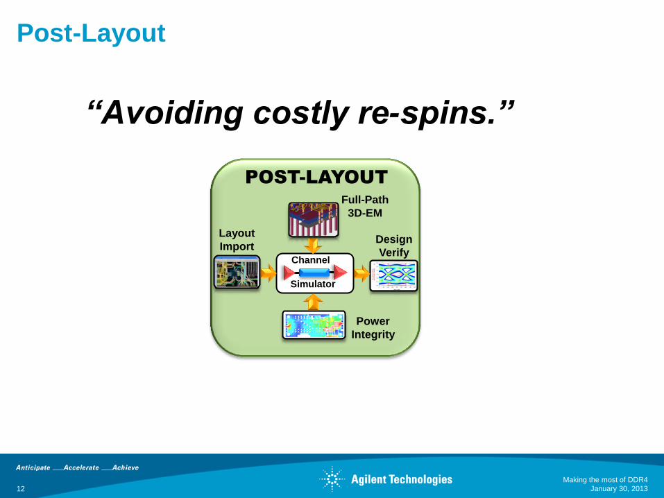
Post-Layout
12
Power
Integrity
Full-Path
3D-EM
Channel
Simulator
POST-LAYOUT
Layout
Import Design
Verify
“Avoiding costly re-spins.”
January 30, 2013
Making the most of DDR4

Post-Layout ADFI for Importing PCB Designs
13
Intelligent Net Selection
Cookie Cutting
Layer Selection Tools
and Fabrication Details 1 2
EM Simulation
3
DQ Signal Eye Diagrams 4
EM
Model
EM
Model
EM S-Parameter Model
Co-Simulation
5 DDR Compliance Report 6
January 30, 2013
Making the most of DDR4

Post-Layout Full EM for Power Integrity
14
U1 U2
U3
U4 U5
U6
U7 U8
U9
SI/PI SETUP TOOL
ADS 3D MOMENTUM VIEWER
Impedance at Each IC, no Caps
POWER INTEGRITY SIMULATION
Samsung DDR3
PC3-UDIMM V102
© JEDEC, permission obtained to
be used in EEsof training examples
January 30, 2013
Making the most of DDR4

Measurement
15
“How Well Does it Work.”
January 30, 2013
Making the most of DDR4

Probing Location and De-Embedding…..
16 January 30, 2013
Making the most of DDR4
DDR4 DRAM Specification is for Performance at the Package Bumps

Optimizing Probe Load and Bandwidth
17
Signal Loading Bandwidth Conflicting Requirements
January 30, 2013
Making the most of DDR4

Measurement Probing Design Requires Simulation
18
In-Situ probing at speed requires inserting
a connection in the signal path.
Simulation optimizes topology as well as
optimum location for accurate probing.
Buried isolation resistor
January 30, 2013
Making the most of DDR4
Where to Go Next…….
19
• Product page http://www.agilent.com/find/signal-integrity-analysis
• Blog http://www.agilent.com/find/signal-integrity
• Self-guided workshop http://www.agilent.com/find/eesof-hsd-workshop2011
• Integrated DesignGuides, Compliance DesignKits, and Examples:
– IBIS AMI, DDR, PCIe, USB, HDMI, SAS2, UHS2
agilent.com/find/signal-integrity
January 30, 2013
Making the most of DDR4