editorial digest - vision-systems.com · editorial digest - vision-systems.com
TRANSCRIPT
Editorial digEst
Machine Vision in solar Cell ManufacturingWith demand for more efficiency, improved quality,
and reduced costs, solar cell manufacturers are
using machine vision systems to meet their goals.
The many manufacturing challenges are being
met by systems based on visible, near-infrared, or
electroluminescent imaging. Among their many
functions, these systems are inspecting for defects,
locating edges, and tracking and packaging solar
wafers through the production process.
This Vision Systems Design Editorial Digest
focuses on the ways in which machine vision can
aid the manufacture of solar cells, with articles on:
- challenges for automated optical inspection
systems throughout the solar cell production
process
- machine vision for edge isolation of solar cells
- inspecting and sorting screen-printed electrodes
- robotic systems for inspection and packaging
2 Uniquely Challenging 9 Machine
vision speeds edge isolation in solar cells
11 SolarScreening 18 Into
the Light
sponsorEd by:
Systemsd e s i g n
VisionSystems®

Capture the power of DALSA Download product specifications and our white paper: “An Introduction to Color Machine Vision” www.dalsa.com/falcon/v10/2010
Falcon cameras are fully compatible with Sapera Essential Vision Software. www.dalsa.com/mv
Falcon VGA300 HG 640 x 480 7.4 µm 300 fps 160 MB/s
Falcon 1M120 HG 1024 x 1024 7.4 µm 120 fps 160 MB/s
Falcon 1.4M100 HG 1400 x 1024 7.4 µm 100 fps 160 MB/s
Compliant with Power Over Camera Link (PoCL) standards
Base Mini-Camera Link
Global Shutter and reset
DALSA Color Cameras provide high color fidelity and
flexibility at low cost. DALSA offers a wide range of color area scan,
line scan and smart cameras, including the Falcon HG series with Bayer
color filter pattern and DALSA’s own CMOS sensor delivering 300 fps.
Falcon HG
DALSA Color Cameras are ideal for Color applications such as:
• Electronics Inspection
• Semiconductor Inspection
• Industrial Metrology (gauging)
• Print Registration
• Flat Panel Inspection
• Other Machine Vision Applications

Vision systems design :: EDITORIAL DIGEST
3
Uniquely Challenging
Solar cell manufacturing faces several AOI challenges that can be met by visible, near-infrared, or electroluminescent imaging
By XInG-FEI HE
although thE EConoMiC situation slowed down
photovoltaic (PV) installation last year, the market
continues to grow. According to the European Photovoltaic Industry
Association (EPIA), the market will reach $31 billion with a capex of
$6 billion in 2010. With oversupply of capacity, solar cell manufacturers are under
pressure to find ways to increase efficiency, improve quality, and reduce costs.
Automated optical inspection (AOI) systems are growing rapidly as the solar
industry is reaching the stage of maturity in which machine vision undergoes
mass adoption on the production floor. A properly designed AOI can help meet
these goals. At some production stages, however, AOI system designers have
unique challenges to overcome.
Silicon-wafer-based solar cells currently represent 82% of the PV market, according
to EPIA. The typical solar cell has a structure (see Fig. 1) that needs a variety of
processing techniques to fabricate, including surface texturization and the silk-
screening of conductor layers for connection of the cell into a panel assembly.
Compared with traditional semiconductor electronics manufacturing processes,
wafer-based solar cell manufacture has some unique processing steps that
create both opportunities and challenges for AOI. While there is no standardized
production flow in the solar-cell manufacturing industry, a typical fabrication
process contains opportunities for AOI to aid in error detection and process
control (see Fig. 2).

Uniquely Challenging
4
Vision systems design :: EDITORIAL DIGEST
An incoming wafer
inspection system looks
at the surface conditions
and geometry of the wafer,
checking for distortion,
chips, saw marks,
contamination, and obvious
cracks. It also looks for
micro-cracks, which are
especially problematic
for solar cell production
because they can result
in a wafer shattering
during the following steps.
Shattering not only results
in yield reduction but can
shut down the production
line for the time needed to
remove the debris.
Other AOI opportunities
include inspecting
texturization, antireflective
coatings, printed
metallization layers, and a
final operational inspection
of the finished cells that
takes advantage of the
solar cell’s electro-optical
characteristics.
Visible imaging
Conventional AOI systems
using visible light can handle a number of these inspection processes. Either
linescan or area-scan cameras can be used depending on the system design.
1002VSDfea1F1
Antire�ection layer
SiO2
p+
nn+
Aluminum
-e
P
+Hole
Ag
PdTi
Si
1002VSDfea1F2
Wafer inspection• Surface and geometry• Micro-cracks• Warpage• Saw grooves and steps• Thickness• TTV
• Texturization control• Etching depth measurement
Cell-classification(FS and BS)
Print inspection (FS and BS)
Additional off-line equipment• Sheet resistance calibration• Contact and line resistance• Optical microscopes• Microbalances• Ellipsometer
• Sheet resistance measurement
Chemical etching
and texturization
Classification
and sorting
Co-firing Backside
printing
(full contact)
Backside
printing (pads)Frontsid
e
printing
Emitter
diffusion
p-glass removal
Silicon
nitride ARC
1 2
3
4
2
5
5
56
6
FIGURE 1. Silicon-wafer-based solar cell structures, typically sized at 156 × 156 mm or 210 × 210 mm with a thickness of 150–200 µm, include antireflection coating, surface texture that helps recapture reflected light, and frontside and backside metallization layers as electrodes.
FIGURE 2. A solar cell production line provides many opportunities for placement of AOI systems, some of which have requirements unique to solar cells. (Courtesy of ICOS, a division of KLA-Tencor)

Uniquely Challenging
5
Vision systems design :: EDITORIAL DIGEST
In the geometry and surface inspection stages, for instance, visible light and a
monochrome linescan or TDI camera will suffice. These types of cameras allow
the inspection to occur in line, as the wafer moves along the production flow. The
size and type of defects for which the system is checking require cameras with
resolution in the range of 2k, 4k, or 8k pixels per line with pixels 7–14 µm in size.
The linescan or TDI rate needs to be fast enough to avoid creating a bottleneck
in the production flow—typically in the 20–100-kHz range depending on the
throughput. In addition, antiblooming or autoexposure features are desirable to
avoid image saturation.
Inspection of the antireflection coatings can also use visible light, but color
camera capability is required. Under white light, the antireflective coating on the
solar cell will appear blue because longer wavelengths transmit more efficiently
while the shorter wavelengths still experience reflection. The exact hue and color
saturation of the reflected light depends on the coating thickness.
Consequently, using the blue channel on a color linescan camera allows detection
of defects as well as process-control measurement. As with the wafer inspection
system, linescan cameras allow inspection of moving wafers. Color cameras with
1002VSDfea1F3b
Wafer travel (one per second)
Linear redLEDs
Linear redLEDs
Linearred
LEDs
DALSAPiranha 3 DALSA
Piranha 2
DALSAPiranha 2
DALSAEclipse
Resistivity/TTVtester(s)
Surfacecontamination
Micro-crack/saw cut
Geometry/chip-out
Linear NIRLEDs
FIGURE 3. The Meikle Automation IS360 Wafer Inspector (left) uses NIR backlighting to detect and measure micro-cracks. The system incorporates DALSA Piranha and Eclipse linescan cameras, which interface to National Instruments Camera Link and LVDS frame grabbers that are installed in high-speed image-processing PCs. The PCs run Meikle’s MASS material-handling and image-processing software. Standard encoder-based image acquisition along with continuous light and speed control ensures consistent image quality. Parallel processing is required to achieve one-wafer-per-second throughput (right).

Uniquely Challenging
6
Vision systems design :: EDITORIAL DIGEST
4k- to 8k-pixel resolution and 20–40-kHz scan
rates are typical.
The metallization print process is another
opportunity for AOI to identify defects and
provide process-control measurements
using conventional cameras and techniques.
Two-camera systems can be used,
providing frontside and backside inspection
simultaneously.
near-infrared imaging using backlight
One of the most demanding AOI challenges is
during the incoming inspection stage: checking
for micro-cracks that can occur during
crystal growth and wafer sawing. This is a
critical checkpoint before beginning the cell
processing, both to ensure yield and to reduce
the occurrence of production downtime due to
a wafer shattering.
However, the micro-cracks can be too small—
less than 5 µm wide—to be seen during a
typical surface inspection. Furthermore,
cracks are difficult to detect using surface
illumination because there is almost no
contrast between the reflections of the crack
and the surrounding silicon.
Instead, this inspection requires the use of backlighting. Because the wafer is
only 150–200 µm thick and silicon is semitransparent in the near-infrared (NIR)
spectrum, LED backlighting using 850–950-nm wavelengths will provide enough
illumination to obtain useful images.
Under these backlighting conditions, a crack will scatter light and create a
dark line against a light background that is readily detectable. Sensors need a
FIGURE 4. Micro-cracks in polysilicon wafers can be captured using NIR backlighting and TDI cameras with sufficient sensitivity at those wavelengths. In the IS360 Wafer Inspector, pre- (left) and post-processed (right) images of micro-cracks are analyzed and the wafers sorted based on their dimensions using proprietary algorithms. (Photo courtesy of Meikle Automation)

Uniquely Challenging
7
Vision systems design :: EDITORIAL DIGEST
resolution of 2–8k pixels with 7–14-µm pixel size to be able to detect these defects.
The challenge is that CCD image sensors lose quantum efficiency (QE) in NIR
wavelengths, resulting in a relatively weak signal. Moreover, camera systems
vary considerably in their NIR sensitivity. Some cameras exhibit as much as
30–40% QE at 900 nm while others can be much lower. Therefore, sensor and
camera selection are critical in developing an AOI system for backlit micro-crack
inspection.
System developers should also consider the exposure time needed to obtain
a usable image under NIR backlight because this directly affects the system’s
production throughput. The shorter the exposure time, the faster the production
line can run at this step.
Increasing the NIR backlight intensity is one option for reducing exposure time
but is limited by the availability of appropriate LED light sources. A more practical
approach is to utilize a time-delay integration (TDI) sensor. These sensors
utilize multiple TDI stages (as many as 100x) synchronized to the scan rate to
accumulate multiple exposures at each stage. The result is the equivalent of a
single line sensor with 100x of sensitivity. For example, DALSA’s Eclipse TDI has
a QE of 32% at 900 nm and 96 TDI stages, which provide a combined broadband
responsivity of 1950 DN/nj/cm2 at 0-dB gain.
Systems for performing backlight inspections have begun to appear. For example,
Meikle Automation developed the IS360 Wafer Inspector (see Fig. 3). As one of its
inspection steps, the IS360 detects and analyzes micro-cracks using proprietary
software and sorts wafers based on the dimension and area information of the
defects (see Fig. 4). These data also provide operators with feedback to improve
process control on the manufacturing floor.
Electroluminescence
Another AOI opportunity unique to solar cell manufacturing, along with
backlit micro-crack wafer inspection, is final quality inspection. This step takes
advantage of the solar cell’s electro-optical characteristics, which allow the cell to
generate luminescence for imaging.

Uniquely Challenging
8
Vision systems design :: EDITORIAL DIGEST
This step can pinpoint micro-cracks and other production-induced defects in
the finished cell/panel that can cause early failure but might not be detectable
via conventional electrical testing. Eliminating defective cells at final inspection
can ensure that solar panels fabricated from the remaining cells have a product
lifetime exceeding 20 years.
The application of a current density of about 40 mA/cm2 to a cell causes
electroluminescence (EL) and results in the emission of light centered at 1.15 µm,
corresponding to silicon’s bandgap energy (1.1 eV). Any defects in the silicon will
appear by inspecting the uniformity of the EL (see Fig. 5). Photoluminescence (PL)
uses a similar method but with laser excitation rather than an electrical current.
The EL process has the additional attribute that the amount of light a cell
generates for a given applied current can serve as a measure of the solar cell’s
conversion efficiency. This means the final inspection step can not only detect
defects, it can help sort and grade finished cells by their output characteristics.
The results can also assist in process control as well as in matching cells for
compatibility in a solar panel assembly.
handling ir insensitivity
While AOI in the final inspection has the potential to provide significant
manufacturing benefits, it also represents a significant challenge for which there
is as yet no ideal solution. The problem is that conventional silicon imaging
sensors have extremely poor sensitivity beyond 1 µm, with a QE of almost zero.
As a result, the inspection requires long exposure times—on the order of
seconds—to obtain usable images. Right now, area-scan cameras are being used
in EL because of the long exposure time required and are creating a bottleneck in
production.
The image sensor industry is actively seeking a better alternative. One approach
is to use indium gallium arsenide (InGaAs) sensor technology, which has greater
sensitivity at 1.1 µm. Unfortunately, it is also expensive. Cameras using InGaAs
sensors cost from $20,000–$40,000, depending on the type of camera.
Also, the resolutions of currently available sensors—1k for linescan or 640 × 512

Uniquely Challenging
9
Vision systems design :: EDITORIAL DIGEST
pixels for area-scan—are not high enough to meet the needs of these inspection
applications. Imaging an entire wafer with sufficient detail would require the use
of multiple cameras, multiplying the already high system cost.
An alternative is to use a fluorescent pigment coating on the silicon sensor.
Infrared photons striking the coating would generate shorter-wavelength
secondary photons, effectively converting the IR to visible light that the silicon
sensor can more readily detect. This conversion is known as an anti-Stokes
process and it has a low conversion efficiency
(0.2~2%), which results in limited improvement in
sensitivity requirements. The coating also could
reduce the sensor’s modulation transfer function,
thereby degrading sensor performance.
While the industry seeks to find a better solution to
EL/PL inspection challenges, the opportunities for
AOI in solar cell manufacturing remain. Many of the
inspection needs can be met with fairly conventional
AOI system designs and allow a tradeoff among
performance and cost to match different production line needs. To address solar
cell production’s unique AOI opportunities, however, developers should seek
effective ways of handling NIR/IR imaging.
XInG-FEI HE is senior product manager of linescan and TDI product lines at
DALSA, Waterloo, ON, Canada (www.dalsa.com).
DALSA,Waterloo, ON, Canadawww.dalsa.com
European Photovoltaic Industry AssociationBrussels, Belgium www.epia.org
ICOS, a division of KLA-Tencor Leuven, Belgium www.icos.be
Meikle Automation Kitchener, ON, Canada www.meiklesolar.com
Company Info

10
Vision systems design :: EDITORIAL DIGEST
Machine vision speeds edge isolation in solar cells
by AnDy WILSOn, Editor
MaChinE-Vision tEChnology is now being used in many stages
of photovoltaic production to supervise and control manufacturing
processes. “In edge isolation systems, wafer classification, and
solar module inspection, machine vision is being used to both
check the quality of individual
process steps and provide
feedback to better understand and
control manufacturing processes
themselves,” says Johannes
Stelter, head of the Intralogistics
and Image Processing Division at
Eckelmann (Wiesbaden, Germany;
www.eckelmann.de), a developer
of control systems for industrial
automation.
Integrated machine-vision systems
are required for the positioning
and measurement of geometric
properties such as edge and chamfer lengths of solar wafers. These systems must
also identify material faults such as microcracks or chips and guide laser-based
systems to provide laser edge isolation.
“Edge isolation provides electrical separation between the active front side of a
solar cell and the rear side,” says Stelter. “In the edge isolation process, a laser
cuts a small groove along the cell edges, the depth of the groove depending on
the width of the doped emitter layer of the cell. The difficulty lies in positioning
the groove as close as possible to the outer contour of the cell to maximize the
Eckelmann’s edge isolation system measures the outer contours of a solar cell and transfers the contour data to the control system of a laser that cuts a fine groove along the cell edges.

Machine vision speeds edge isolation in solar cells
11
Vision systems design :: EDITORIAL DIGEST
active surface and thus the efficiency of the solar cell.”
To develop a laser edge isolation system for the Asys Group (Dornstadt, Germany;
www.asys.de), a manufacturer of handling systems and process machines for
the electronic and solar industries, Eckelmann teamed with Stemmer Imaging
(Puchheim, Germany; www.stemmer-imaging.de) to produce a system based
on linescan cameras that can measure the outer contours and transfer contour
data to the control system of a deflection mirror-based laser etching system (see
figure). Edge damage is detected and, if the damage is within tolerance levels, the
system proceeds with the cutting process.
To perform this task, images of each 125- or 156-mm square wafer is illuminated
with custom LED lighting and digitized with a 4k Piranha Color, 17-kHz linescan
camera from DALSA (Waterloo, ON, Canada; www.dalsa.com) fitted with a
Distagon 28-mm lens from Carl Zeiss (Oberkochen, Germany; www.zeiss.de).
Placed 300 mm above the solar cell to be inspected, the cameras is moved at 680
mm/s on a gantry, which results in a field of view of approximately 165 × 165
mm, producing images each of 4096 × 4096 pixels.
As the solar panel is moved across the camera’s field of view, images are
digitized into a PC using an X64 Xcelera-CL, also from DALSA, and edge
detection image analysis is performed. As the laser engraves the edge isolation
grid into the solar cell, grid distances are measured by the camera and any
differences in this value and the expected value are used to compensate for
nonlinear errors that may occur.
“Image acquisition and analysis take place in 800 ms,” says Stelter. The resolution
of the system makes it possible to ensure that laser edge isolation can be
performed less than 100 µm from the edge of the wafer.
Because the laser and camera system are automatically calibrated by the
machine-vision system, recalibration can be automatically performed after any
maintenance work. The system calculates a compensation map that is used for
error correction in the control system of the laser deflection unit. Errors in the
transport system of the machine can be also be diagnosed using the image-
processing system, thus allowing for remedial action to be taken.

DALSA Color Cameras provide high color fidelity and flexibility at low cost. DALSA offers a wide range of color area scan, line scan and smart cameras, including the BOA vision system with on board features such as multiple processing engines combining DSP, FPGA and CPU technologies. BOA has a tiny form factor,
easy mounting capabilities and has an IP67 rating.
BOA Next generation Smart Camera
VGA (640 x 480) Color CCD Sensor
Capture the power of DALSA Download your BOA product brochure here: www.dalsa.com/boa/v10/2010
Embedded point-and-click software - easy to use & nothing to install.
DALSA Color Cameras are ideal for Color applications such as:
• Packaging- Bottle cap color and label confirmation
• Pharmaceutical- Verify pill count and color
in blister pack
• Automotive - Inspect color or texture of interior parts - Verify order of color wires in harness
• General Machine Vision

13
Vision systems design :: EDITORIAL DIGEST
Solar Screening
Machine vision and robotics inspect and sort screen-printed electrodes, improve solar-cell manufacturing yields
By C.G. MASI, Contributing Editor
photoVoltaiC solar CElls start out as silicon wafers a fraction of
a millimeter thick. They are then trimmed to square or rectangular
shape a few inches across. The manufacturer also chamfers the corners
to reduce the possibility of
breakage. Subsequent processing steps
add several thin- and thick-film coatings
that give the cells the ability to convert
sunlight into electric power and channel
that power to a useful load.
Working with manufacturers of solar
cells, Adept Technology has been helping
automate several steps in the production
process. Recently, the company
developed a system to automate the
quality-control step between screen-
printing the final set of electrodes onto
cell surfaces and baking them to make
permanent metallic connections.
Before baking, any flawed patterns of the conductive ink can be washed off
and replaced, thus saving the wafers. After baking, such flawed wafers must be
discarded, wasting the cost of the silicon material and the value added by the
processing steps up to that point.
Robotic wafer-handling station uses grippers such as suction cups (shown) or those based on the Bernoulli principle to lift and sort solar wafers after inspection.

Solar Screening
14
Vision systems design :: EDITORIAL DIGEST
automated inspection
The machine-vision-based automated inspection system and the robotic wafer
handler sit between the screen-printing station and bake oven on the electrode-
printing production line (see Fig. 1). This is the next-to-last step in the production
process, and wafers have already gone through several thin-film coating
procedures to make them convert light to electricity efficiently.
The final step, adding
the electrodes, is
needed to channel
electricity out of the
wafer. Once wafers
leave the oven, they
need only a clear
conformal coating to
protect active layers
Adept Technology found that the existing production process at a solar cell
manufacturer was bogged down by reliance on manual inspection to ensure
the quality of screen-printed electrodes before they were permanently baked
onto silicon wafer surfaces. “With several different people looking at wafers
from shift to shift,” Todd Reynolds, applications engineer at Adept, says, “one
person rejects more cells that should pass, and others pass more cells that
should have been rejected.
“Combining machine vision and robotics allows for less waste,” he
adds. “We’re able to look for things like length and width of wafer.
That allows us to get a refined center for the wafer for handling
with robots. We can find chips and cracks on the wafer and
inspect the printed lines for a variety of different defects.”
Improving throughput and yield near the end of the production
process will have a major impact on total manufacturing cost.
Reject bins
Screenprintingstation
Automatedinspection
station
Wafer-handling
robot
A B C D
Oven
Toconformal
coatingstation
0907VSDfea2profilF1FIGURE 1. Combining machine vision and robotics for automated inspection before baking electrodes onto wafers improves process yield.

Solar Screening
15
Vision systems design :: EDITORIAL DIGEST
from environmental effects before shipping to customers. Wafer losses at this
point are maximally expensive, so high yield is critical.
Printing is a silk-screening process that lays down a pattern of conductive-ink
electrodes. The ink consists of fine metal particles suspended in a two-part fluid
consisting of a volatile solvent and an organic binder. After the screen pattern
has been laid down, the solvent rapidly
evaporates, leaving the metal particles
held in place by the binder.
This is the stage at which it pays to
inspect the pattern and recycle wafers
with printing flaws. At the same time,
cracks, contamination, and any other
flaws in the wafers are investigated.
The inspection unit mounts into a light
shield shaped like a truncated pyramid
mounted over the conveyor line
carrying wafers (see Fig. 2). The camera
mounts in the upper portion, and a row
of LED lights on either side of the conveyor illuminates wafers as they come by.
The conveyor runs at a constant speed, with the LEDs being strobed to stop the
motion.
At 26-in. high and covering a 12-in.2 footprint, the inspection unit is designed
to mount 1 in. above the conveyor. This allows the light shield to exclude most
ambient light while allowing wafers to move freely on the conveyor. The LED light
lines are positioned so that specular reflections from the wafer surfaces miss the
camera aperture and are absorbed by the light shield’s inner surface.
The system uses a Basler piA2400-12gm Gigabit Ethernet camera connected to
Adept’s proprietary Smart-Vision EX vision controller. The unit is a PC-based
vision controller running the company’s Automation Control Environment (ACE)
and AdeptSight machine-vision software.
LEDField ofview
Camera
Wafer
Lightshield
Reflectionsmiss camera
FOV
Lens
Conveyor
LED
0907VSDfea2profilF2FIGURE 2. Placing lines of LEDs within a light shield illuminates conductive ink traces while avoiding specular reflections.

Solar Screening
16
Vision systems design :: EDITORIAL DIGEST
ACE is an integrated, point-and-click development environment with
configuration tools and basic programming features for robotics applications.
AdeptSight includes utilities for vision-guided and inspection applications.
The twin requirements of automated inspection and robot guidance call for
different analysis algorithms applied to the same image. As the wafer moves
on the conveyor, the
first step is to acquire
an image from the
camera and upload
it over the GigE
connection to the
vision controller for
processing.
Thresholding and
edge finding bring out
the wafer outline as
well as highlighting
the screen-printed
electrodes. Inspection
tasks are broken into
three areas: print inspection, inspection for chips, and pattern recognition. Print
inspection ensures the electrode edges are crisp, form the correct pattern, and
are properly registered with the wafer edges (see Fig. 3).
Inspection for chips ensures that the wafer outline does not vary from the correct
size and shape: All edges must be straight; dimensions must be correct; and the
corner chamfers must also be correct. Cracks appear as extraneous irregular
lines that can be highlighted by enhanced contrast and thresholding. Pattern-
recognition algorithms search for anything out of the ordinary such as cracks or
broken ink lines. Linear measurement algorithms verify correct placement of ink
patterns that are supposed to be there.
Wafer handling
The wafer-handling station following the inspection uses an Adept Quattro
Figure 3. The machine-vision software locates a wafer with a refined center. Both busbars have been located and inspected for width, length, and defects (e.g., skips in the printing, bulges, necking).

Solar Screening
17
Vision systems design :: EDITORIAL DIGEST
robot with an unusual robotic gripper and coordinates with the vision system to
automate both the inspection and handling of the wafers. The Quattro robot is a
variation of the fastest type of robot available: the delta robot.
The older delta robot design has three “arms” attached to a “base” mounted over
the work space. Each arm consists of an upper member—which is driven by a
servomotor built into the base—and a lower member attached to a platform that
carries a gripper (or whatever end effector the application calls for).
Passive joints at the lower member’s ends allow the arms to flex in a coordinated
way under the influence of the separately controlled servomotors. A rod driven
by a fourth servomotor rotates the gripper as needed, providing the robot with a
fourth degree of freedom.
Calculating servomotor rotations to effect a required motion, however, is more
complicated for a delta-robot controller than for, say, a conventional six-axis
selective compliant articulated robot arm (SCARA) because the delta robot’s
control degrees of freedom do not match any spatial
coordinate system. To make a motion along any given axis
requires coordinated action of all servomotors.
The Quattro robot differs from delta designs by having a
fourth arm and no central rod. The rotational degree of
Platform(springs not shown)
Outer arms
Ball joints(springs not shown)
Motorcover
Base
AIBCable cover
(IP-66 option)
Innerarms
Mountingpads
0907VSDfea2profilF3b
FIGURE 4. Adept’s Quattro robot is a modification of the delta robot configuration. Unlike delta robots, the Quattro robot rotates its platform by shifting
“shoulders” in the base.

Solar Screening
18
Vision systems design :: EDITORIAL DIGEST
freedom is made possible by providing “shoulders” in the base that move the robot’s
four arms relative to each other. This arrangement makes it possible to increase
the Quattro robot’s strength, speed, and agility relative to delta designs, but it also
further complicates the motion controller’s kinematic calculations (see Fig. 4).
In another departure from conventional material-handling robot practice, rather
than use a more traditional suction-gripper technology to pick up and move
wafers, Adept’s design uses a gentler method based on Bernoulli’s principle.
Suction grippers use vacuum to pull the wafer against an elastomeric cup.
Friction between the cup lip and the wafer then provides the force needed to
move the wafer.
Bernoulli’s principle, on the other hand, shows how to use positive air pressure to
pull the wafer close to, but not in contact with, a flat plate. The principle says that
along a streamline, air pressure is inversely proportional to air speed squared.
Air forced through a narrow gap between the gripper plate and wafer must move
rapidly to escape. Once outside the gap, the air effectively slows to a stop. Thus
air pressure in the gap must be much lower than atmospheric. Ambient pressure
will press the wafer
close to, but not in
contact with, the
plate. The wafer
cannot make contact
with the plate, since
that would block the
airflow and remove
the effect.
ServomotorsInverters
Motion controller
Smart-Vision EXvision controller
Strobecontroller
Camera
Quattrorobot
LEDs
0907VSDfea2profilF5
FIGURE 5. The vision controller sends information via FireWire about part locations and motion control to a motion controller and multiaxis servomotor drive housed in the robot’s base.

Solar Screening
19
Vision systems design :: EDITORIAL DIGEST
Suction grippers create a concentrated stress around the suction inlet port,
whereas the Bernoulli gripper spreads the stress over the whole gripper plate.
This phenomenon greatly reduces the maximum stress level in the wafer and
subsequent breakage.
robot guidance
Robot guidance needs are fairly simple. The robot needs to know exactly where
the wafer center is on the conveyor and what its orientation is so that it can
correctly pick up any wafer that needs to be moved and avoid collisions during
movement. The vision controller sends information via FireWire about part
locations and motion control to a motion controller and multiaxis servomotor
drive housed in the robot’s base (see Fig. 5).
Observing the angles that edges make with the image frame provides orientation
information. The controller can then transform to a rotated coordinate system
aligned with the wafer edges. This also helps the wafer inspection task. Finally,
finding the wafer center is a matter of averaging the coordinates of opposite edges
and rotating the results back to the conveyor-based coordinate system.
It would be possible to determine the conveyor speed
by calculating wafer-center locations in two subsequent
images, but it is better to rely on sensors built into
the conveyor system. A vision-based measurement
only provides one average speed measurement during
a particular time interval and cannot capture slight
variations in conveyor speed that might affect positioning
by the time a wafer reaches the robot position. Conveyor speed sensors, on
the other hand, can provide constant real-time monitoring for more accurate
positioning.
For wafers that do not pass inspection, the vision controller has to decide
into which of four reject bins they should go: those that can be cleaned and
reprocessed, and those with different kinds of uncorrectable defects, such
as corner chips, edge chips, and cracks. Since different defects arise from
different causes, separating according to defect type helps continuous process
improvement efforts.
Adept Technology Pleasanton, CA, USAwww.adept.com
Basler Vision ComponentsAhrensburg, Germany www.baslerweb.com
Company Info

20
Vision systems design :: EDITORIAL DIGEST
Into the Light
Vision-guided robotic systems inspect and package solar cell wafers
by JOyCE LAIRD, Contributing Editor
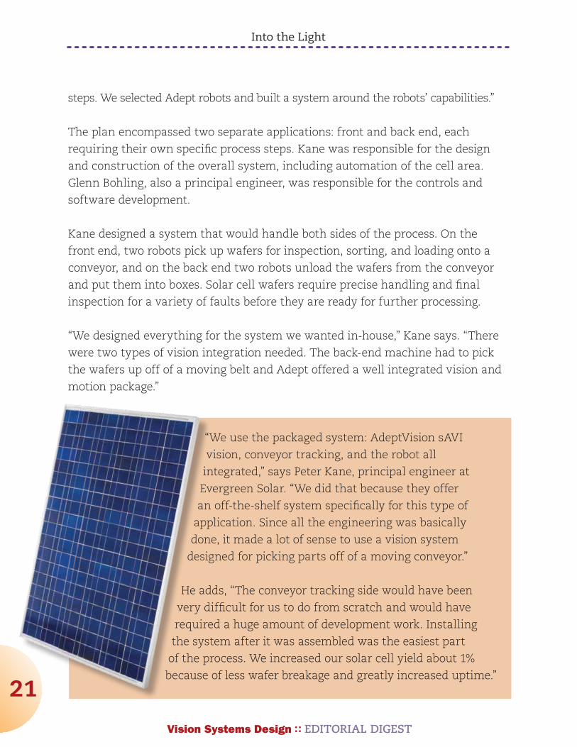
EVErgrEEn solar produCEs solar panels using its proprietary
crystalline silicon technology known as String Ribbon. To manufacture
the wafers that form the basis for the panels of solar cells, parallel wires
or strings are pulled through a silicon melt and the molten silicon spans
and solidifies between the strings, creating a long ribbon that is periodically
harvested for processing into solar cells. This unusual method of developing solar
cells has proved to be simple, efficient, and commercially successful.
Success has required greater
processing speed to meet demand.
The original gantry fixed automation
system developed in-house to handle
the inspection, sorting, and packing
steps was becoming too costly to
maintain and required five pickup
steps to move the pre-etched silicon
wafers to their final destination after
they had been acid-etched to clean
the surfaces.
Peter Kane, principal engineer at
Evergreen, says that the less the wafers
are handled the better. “We decided
that going to a robotic system could
bring this handling down to only two
FIGURE 1. Robots pick wafers for inspection in the Evergreen Solar pre-etch inspection, sorting, and packaging machine.
Into the Light
21
Vision systems design :: EDITORIAL DIGEST
steps. We selected Adept robots and built a system around the robots’ capabilities.”
The plan encompassed two separate applications: front and back end, each
requiring their own specific process steps. Kane was responsible for the design
and construction of the overall system, including automation of the cell area.
Glenn Bohling, also a principal engineer, was responsible for the controls and
software development.
Kane designed a system that would handle both sides of the process. On the
front end, two robots pick up wafers for inspection, sorting, and loading onto a
conveyor, and on the back end two robots unload the wafers from the conveyor
and put them into boxes. Solar cell wafers require precise handling and final
inspection for a variety of faults before they are ready for further processing.
“We designed everything for the system we wanted in-house,” Kane says. “There
were two types of vision integration needed. The back-end machine had to pick
the wafers up off of a moving belt and Adept offered a well integrated vision and
motion package.”
“We use the packaged system: AdeptVision sAVI
vision, conveyor tracking, and the robot all
integrated,” says Peter Kane, principal engineer at
Evergreen Solar. “We did that because they offer
an off-the-shelf system specifically for this type of
application. Since all the engineering was basically
done, it made a lot of sense to use a vision system
designed for picking parts off of a moving conveyor.”
He adds, “The conveyor tracking side would have been
very difficult for us to do from scratch and would have
required a huge amount of development work. Installing
the system after it was assembled was the easiest part
of the process. We increased our solar cell yield about 1%
because of less wafer breakage and greatly increased uptime.”

Into the Light
22
Vision systems design :: EDITORIAL DIGEST
The robotic system uses the Adept Cobra s800, a SCARA-type robot, and includes
the Adept SmartServo controls architecture that supports options such as
conveyor tracking and vision-guided motion. The diagnostics display enables
troubleshooting, and the robot has integrated temperature sensors to monitor
heat in servo motors to prevent damage.
system design
On the front end, the system is required to pick wafers out of boxes and move
them to a camera station to inspect the wafers for imperfections such as
cosmetic defects, edge defects, and cracks. It also needed to determine x-y and
theta position of the wafers when placing them on the conveyor (see Fig. 1).
“We use the ePLC version of the 800 robot for this,” Kane says. “An Allen Bradley PLC
controls each robot and it also talks to the vision system. We use two Cognex DVT
540 smart cameras, which include a processor, image sensor, the optics, and light.”
The Adept ePLC Connect Server software provides connectivity with the PLC.
All application programs and locations are defined and reside within the Allen
Bradley PLC. The PLC client retrieves this data and commands the robot to move.
The robot lifts an individual wafer from a box, moves it over the camera, which is
located below the conveyor; LED lights on the robot provide additional backlighting
for the camera. The wafers are visually inspected; rejects are set aside. The
software records the processing data for statistical process control (SPC) recall and
evaluation. Reasons for rejects are noted. If they pass inspection, wafers are placed
on the conveyor to be moved through the acid wet bench (see Fig. 2).
0810VSDfea3F2
Product flow
Productflow
LoaderAdept ePLC Cobras with LED lighting
and two Cognex DVT cameras
Wet bench
UnloaderAdept dual s800 Cobras withfluorescent backlighting and
conveyor tracking with vision
FIGURE 2. To inspect solar cell wafers, two robots unload boxes, place wafers on a con veyor after inspection by a smart camera for sorting and acid wash, and then load them into boxes after a final inspection.

Into the Light
23
Vision systems design :: EDITORIAL DIGEST
Kane says that Evergreen has
used the DVT cameras for
many other machine-vision
applications within the plant,
so the company is familiar
with the benefits of these
smart cameras. The Cognex
DVT system uses a Hitachi
SH4 processor and has 64
Mbytes of RAM and 16 Mbytes
of flash memory. The CCD
camera operates at 75 frames/s
and supports partial frame
acquisition.
The smart camera
communicates through
Ethernet and RS-232. Vision tool
support includes identification
(modeling), readers (ID, 2-D,
OCR/OCV), flaw detection, and
application-specific scripting.
The camera can analyze for odd
shapes and inspect for multiple
and overlapping parts in a
range of light conditions, which
means it is suitable for robotic
guidance.
“We use the Allen Bradley ControlLogix PLC platform and DVT vision with
standard lenses; there is nothing really proprietary here,” Bohling says. “We use
a state diagram system. All the PLC programming is based on state diagrams,
which detail the logic flow of the machine sequences.
“We use custom Visual Basic operator interface applications,” he adds. “We
developed these in-house. It’s standard on all of our machines so that any
FIGURE 3. The operator interface is a customized GUI that is standard on all plant equipment.
FIGURE 4. At the pre-etch unloader end, vision-guided Cobra dual s800 robots pick the wafers from the conveyor and load them into boxes.

Into the Light
24
Vision systems design :: EDITORIAL DIGEST
operator can go to any machine in the plant and
know how to use it.” (See Fig. 3).
Front and back
On the out-feed end, a Dorner conveyor was used,
incorporating simple fluorescent backlighting.
The wafers pass over a backlit area so the out-
feed robots’ integrated vision systems can capture
a binary image of a black wafer against a white
background, inspecting for cracks and chips.
The unloader is a fully equipped Adept Cobra dual
s800, which uses a single controller to control both
robots with sAVI Vision and conveyor tracking. It coordinates robotic movement
with wafers being presented on a moving conveyor (see Fig. 4). Each unloader
robot incorporates an RS-170 camera to inspect the wafers. Any wafer that fails is
not picked up and instead drops off the end of the conveyor into a reject bin.
The entire robotic integrated system for loading/inspection and unloading/
packing was built at the Evergreen plant offline. It took one day to dismantle and
move the old gantry system out and install the new system.
Evergreen currently has 10 Adept robot systems running at its plant in
Marlborough, MA. The downtime for maintenance has been essentially
eliminated in comparison to the old gantry-based automation system that was
down for maintenance at least once a week. The conveyors, PLC controllers, and
cameras had all been in use on other systems within the plant, and proved robust
and reliable when integrated with the robots.
Adept Technology Livermore, CA, USA www.adept.com
Cognex, Natick, MA, USAwww.cognex.com
Dorner Manufacturing Hartland, WI, USA www.dornerconveyors.com
Evergreen Solar Marlborough, MA, USA www.evergreensolar.com
Rockwell Automation Allen Bradley Control Systems Milwaukee, WI, USA www.ab.com
Company Info

25
Vision systems design :: EDITORIAL DIGEST
DALSA Corporation (www.dalsa.com) is an international technology leader in the design, development, and manufacture of digital imaging products and solutions. In addition, DALSA specializes in the engineering and fabrication of semiconductor components and services. The company has grown and currently employs approximately 1000 people world-wide with sales offices across North America as well as in Europe and Asia supporting an international distribution network serving more than 40 countries. Today, DALSA image sensors, cameras, frame grabbers and software are used in thousands of automated inspection systems around the world and across multiple industries including semiconductor, flat panel display, electronics, and manufacturing.
links:
DALSA capabilities in Aerospace and Defense
The Power of Next Generation GigE Vision v1.2
Get More Vision. DALSA’s 2010 Machine Vision brochure.
New HS Interface: Next Generation Camera-to-frame grabber Interface.
DALSA Industrial Vision Solutions brochure.