ee 261 – introduction to logic circuits module #8 page 1 ee 261 – introduction to logic circuits...
TRANSCRIPT

EE 261 – Introduction to Logic Circuits Module #8Page 1
EE 261 – Introduction to Logic Circuits
Module #8 – Programmable Logic & Memory
• Topics
A. Programmable Logic
B. Memory Devices
• Textbook Reading Assignments
6.3, 9.1-9.6
• Practice Problems none
• Graded Components of this Module 1 homeworks, 1 discussion, 1 quiz
(all online)

EE 261 – Introduction to Logic Circuits Module #8Page 2
EE 261 – Introduction to Logic Circuits
Module #8 – Programmable Logic & Memory
• What you should be able to do after this module
Understand the construction and operation of various programmable logic devices (PLD, PLA, PAL, FPGA)
Understand the terminology and functional operation of various memory storage devices (RAM, ROM, SRAM, DRAM, MROM, PROM, EPROM, EEPROM)
EE 261 – Introduction to Logic Circuits Module #8Page 3
Programmable Logic
• Programmable Logic Devices (PLD)
- when combinational logic gets large, it becomes impractical to implement using discrete devices
- an alternative to an Application Specific Integrated Circuit (ASIC) is a programmable logic device
- there are many types of programmable logic to choose from, each with advantages/disadvantages
- PLA - PAL - CPLD - FPGA
- the type of programmable device we target can influences how we minimize/synthesize our logic

EE 261 – Introduction to Logic Circuits Module #8Page 4
Programmable Logic
• Programmable Logic Array (PLA)
- a PLA is a 2-level AND-OR configuration that implements SOP expressions
- a PLA has:
- n inputs - m outputs - p product terms
- inputs are initially buffered and inverted to always create X and X’ literals
- fuses (or reconfigurable switches) are used to selectively connect the literals to the AND level
- fuses are again used to decide which product terms are connected to the OR level
- pull-ups on the lines can produce constant outputs
- logic configurations can also produce constant outputs

EE 261 – Introduction to Logic Circuits Module #8Page 5
Programmable Logic
• Programmable Logic Array (PLA)
ex) 2-input, 2-output, 2-product term PLA the X’s represent where the fuses can be left connected or blown

EE 261 – Introduction to Logic Circuits Module #8Page 6
Programmable Logic
• Programmable Array Logic (PAL)
- a PAL is an extension of a PLA but uses a fixed OR stage instead of a programmable one
- since 0’s going into an OR have no effect, this is possible
- a PAL also has some additional functionality
- Output enables - Output feed back
• Complex Programmable Logic Devices (CPLD)
- multiple PLA’s/PAL’s/PLD’s can be put on one chip with a matrix of programmable interconnect
- this is called a CPLD and gives the ability to begin building a system on a chip

EE 261 – Introduction to Logic Circuits Module #8Page 7
Programmable Logic
• What is an FPGA
Field Programmable Gate Array
• An FPGA uses Re-configurable Logic Blocks
- we set the config bits of this block to set its Boolean logic function
- the configuration is a Truth Table (or Look Up Table) of functionality
OutIn1
In2
config
config Out000 NOT(In1)001 NOT(In2)010 OR011 NOR100 AND101 NAND110 XOR111 XNOR

EE 261 – Introduction to Logic Circuits Module #8Page 8
Programmable Logic
• LUTs = Look Up Tables
- we can program the LUTs to be whatever type of gate is needed by the design- there are a finite number of LUTs within a given FPGA (also called "resources")
• The LUTs are configured into an ARRAY on the silicon
- Array of LUT's = Array of Gates = Gate Array
OutIn1
In2
config
OutIn1
In2
config
OutIn1
In2
config
OutIn1
In2
config
OutIn1
In2
config
OutIn1
In2
config
OutIn1
In2
config
OutIn1
In2
config
OutIn1
In2
config

EE 261 – Introduction to Logic Circuits Module #8Page 9
Programmable Logic
• Programmable Interconnect
- there are programmable interconnect switches that connect the LUTs
LUT LUT LUT
LUT LUT LUT
LUT LUT LUT
X
X
X
X
X
X
X
X
X
X
X
X
X X X
XX

EE 261 – Introduction to Logic Circuits Module #8Page 10
Programmable Logic
• Configuration
- We start with a Gate Level Schematic of our design (from synthesis)- The FPGA LUTs are configured to implement Gates
LUT LUT LUT
LUT LUT LUT
LUT LUT LUT
X
X
X
X
X
X
X
X
X
X
X
X
X X X
XX

EE 261 – Introduction to Logic Circuits Module #8Page 11
Programmable Logic
• Configuration
- The interconnect switches are then programmed to implement the net connections
LUT LUT LUT
INV OR LUT
INV AND LUT
X
X
X
X
X
X
X
X
X
X
X
X
X X X
XX
A
B
C
Out

EE 261 – Introduction to Logic Circuits Module #8Page 12
Programmable Logic
• Configuration
- The LUT and Interconnect configuration is volative (i.e., it goes away when power is removed)
- Since the programming is done by the user after fabrication, we call it "Field Programmable"
- We now understand where Field Programmable Gate Array
LUT LUT LUT
INV OR LUT
INV AND LUT
X
X
X
X
X
X
X
X
X
X
X
X
X X X
XX
A
B
C
Out

EE 261 – Introduction to Logic Circuits Module #8Page 13
Programmable Logic
• Adding More Functionality
- FPGA manufacturer's quickly learned that Flip-Flops would be useful
- They put a DFF next to a 4-Input LUT to form a "Configurable Logic Block" (CLB)
CLB CLB
CLB CLB
X
X
X
X X

EE 261 – Introduction to Logic Circuits Module #8Page 14
Programmable Logic
• Adding Even More Functionality
- To Improve performance, common logic functions were "hard coded" on the silicon
- Block RAM - Adders / Multipliers - Global Clock Buffers - even Microprocessors!

EE 261 – Introduction to Logic Circuits Module #8Page 15
Programmable Logic
• What else can we program?
- Which Pins to use on the package
- What logic levels
- CMOS_33, CMOS25 - SSTL, SSTL2, etc…

EE 261 – Introduction to Logic Circuits Module #8Page 16
Memory Devices
• Memory Classes
- memory refers to a device which stores information
- we’ve seen that Flip-Flops and Latches are a type of memory
- Flip-Flops and Latches tend to take up a lot of area so they aren’t used for high density applications
- instead, there are a variety of other circuits that can hold digital information
- memory is classified into two categories
“Volatile” - when the power is removed, the information is lost
“Non-volatile - the information is held when the power is removed

EE 261 – Introduction to Logic Circuits Module #8Page 17
Memory Devices
• Random Access Memory (RAM)
- RAM means that any location in memory can be accessed
- this is different from “Sequential Access” like a tape or hard drive
- there are two basic types of RAM
1) SRAM = Static RAM 2) DRAM = Dynamic RAM
EE 261 – Introduction to Logic Circuits Module #8Page 18
Memory Devices
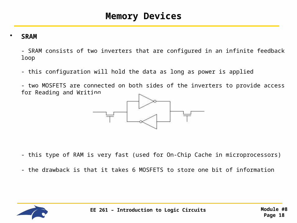
• SRAM
- SRAM consists of two inverters that are configured in an infinite feedback loop
- this configuration will hold the data as long as power is applied
- two MOSFETS are connected on both sides of the inverters to provide access for Reading and Writing
- this type of RAM is very fast (used for On-Chip Cache in microprocessors)
- the drawback is that it takes 6 MOSFETS to store one bit of information

EE 261 – Introduction to Logic Circuits Module #8Page 19
Memory Devices
• DRAM
- DRAM provides information storage using a capacitor
- to access the capacitor, one MOSFET is used
- DRAM is able to store the information in less area than SRAM
- the drawback is that over time the capacitor loses it charge
- to address this, a “Refresh Cycle” is used
- to refresh the capacitor, the circuit reads the value periodically and then writes that same value back to the cell
- this recharges the capacitor fully to its original level
- this Refresh Cycle adds complexity to the access circuitry, however the overall size of the DRAM cell is smaller than an SRAM cell

EE 261 – Introduction to Logic Circuits Module #8Page 20
Memory Devices
• Types of Non-Volatile Memory
MROM - Mask Read Only Memory - during fabrication, 1’s and 0’s are hard coded to VDD and GND - “Mask” refers to the photolithography step during fabrication
PROM - Programmable Read Only Memory - Programmed using High-Voltage to blow fuses on-chip to create 1’s and 0’s - Cannot be un-done, this is a one-time program
EPROM - Erasable Programmable Read Only Memory - Programmed using high-voltage to inject electrons into a “Floating Gate” of a special type of MOSFET. The abundance of electrons will turn on the MOS creating a 1 or 0 - Erased using Ultra-Violet light in order to put the floating gate back to its original state EEPROM - Electrically Erasable Programmable Read Only Memory - Programmed and Un-Programmed using high-voltage - This allows in-system reconfiguration

EE 261 – Introduction to Logic Circuits Module #8Page 21
Module Overview
• Topics
- Programmable Logic - PLA - PAL - CPLD - FPGA
- Memory - volatile / non-volatile - SRAM, DRAM - MROM, PROM, EPROM, EEPROM