ee 271 final project - towers of hanoi - · pdf fileee 271 final project - towers of hanoi...
TRANSCRIPT

EE 271 Final Project - Towers of Hanoi
Siyu Jian, Michael Molina, Kendrick Tang
December 6, 2012
Abstract
In this project, we designed and implemented the game of tower ofHanoi on the DE1 Board. The lab specification asked for a three ringgame, but we went beyond that and gave the user the ability to selectthe number of rings they played with. Our implementation of the designwas successful: it utilizes several databusses to move the right ring tothe right tower if user selects a valid pair of towers, and waits for a validpair otherwise. One difficulty we came across was implementing the GALchip. The display unit had more input and output ports than the GALchip could implement, so we were limited to using the GAL chip as amodule to count the number of seconds it took for the user to finish thepuzzle. Unfortunately, we were unable to finish this extra feature due totime constraints. Regardless, our game still runs very effectively.
We all worked together. We checked each other’s work, helpe debug, code,design, and test our product, but we couldn’t have done it without Kendrick’samazing design and debugging skills. By signing below, we all agree to thisstatement to some degree.
Signature
Signature
Signature Kendrick Tang (digitally signed December 6, 2012)
1
We all worked

2 of 24 EE 271 Lab 4
Contents
1 Introduction 3
2 Design Specification 3
3 Design Procedure 33.1 On the FPGA . . . . . . . . . . . . . . . . . . . . . . . . . . . . . 33.2 On the GAL Chip . . . . . . . . . . . . . . . . . . . . . . . . . . 8
4 Hardware Implementation 9
5 Test Plan 115.1 Game Controller Module . . . . . . . . . . . . . . . . . . . . . . . 115.2 Ring Mover Module . . . . . . . . . . . . . . . . . . . . . . . . . 12
6 Results 136.1 Results of Game Controller . . . . . . . . . . . . . . . . . . . . . 136.2 Results of Ring Mover . . . . . . . . . . . . . . . . . . . . . . . . 136.3 Results of Tower of Hanoi . . . . . . . . . . . . . . . . . . . . . . 14
7 Error Analysis 14
8 Reasons for Incomplete Project 15
9 Summary 15
10 Conclusion 15
11 Appendix 16

3 of 24 EE 271 Lab 4
1 Introduction
The purpose of this lab was to reflect on the knowledge accumulated from therest of the quarter and to design from start to finish our own project. Wewere able to experience firsthand all phases of a project from design, debugging,redesigning, debugging, implementing, integrating and testing, and debugging.Furthermore, due to the unrestricted nature of the guidelines, our design hadno template to help us get started and was limited only by our imagination andcreativity. In other words, the design was completely up to us. How robust ourgame was, was also completely up to us. We were in charge of determining testvectors, boundary cases, user errors, backup systems and error prevention all onour own, which tested our ability to find and balance all possible cases of errorwith practicality. We implemented our design of the Towers of Hanoi game onthe DE1 board. We used almost every single output port from the breadboard,but also all the switches, buttons and LEDs for user input and debugging. Withaccess to the 18 LEDs on the board itself, we were able to observe and verify thecondition of our state machines, as well as values of different input and outputvectors simultaneously.
2 Design Specification
In general, this lab only specified us to design a functional game on an FPGAboard. We chose to create the Towers of Hanoi game. This game starts witha number of rings stacked on one peg, where each ring is smaller than the onebelow it. From there, rings are moved between three pegs, where a ring canonly be placed on a ring that is larger than it. The winning condition is whenthe user has successfully transferred all the rings on the first tower to the thirdtower. Nobody can play the game without being able to see the state of therings and towers, so a visualizer or display unit was essential to this design.Additional specifications were to use a databus to transfer information betweenregisters, and implement a GAL chip as an external module. We decided toimplement a game timer on the GAL chip as an additional feature to the game.
3 Design Procedure
3.1 On the FPGA
The design boiled down to capturing a way to encode the tower information, anda way to manipulate the information. We needed to not only encode how manyrings were in each tower, but also the size of each ring in the tower. Furthermore,we needed to use this information to restrict the possible moves the user coulddo. We decided to use a seven bit register to represent each tower, where theleast significant bit represented whether the largest ring was present, and themost significant bit represented whether the smallest ring was present. This way,a pair of choices is valid only if the value held in the register that representsthe first choice is greater than the value held in the register that represents the

4 of 24 EE 271 Lab 4
second choice. To manipulate the information, we used combinational logic toencode the value of a tower register in a one-hot binary value where the activebit represented the topmost ring. From here, all that needed to be done was tosubtract the one-hot value from the first choice, and add it to the second choice.We utilized two modules to implement this design:
Figure 3.1: High level design for the entire system.
5 of 24 EE 271 Lab 4
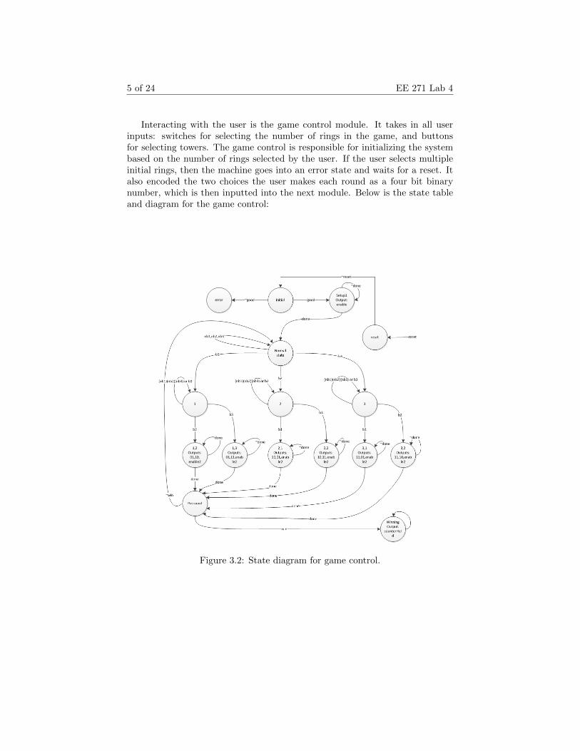
Interacting with the user is the game control module. It takes in all userinputs: switches for selecting the number of rings in the game, and buttonsfor selecting towers. The game control is responsible for initializing the systembased on the number of rings selected by the user. If the user selects multipleinitial rings, then the machine goes into an error state and waits for a reset. Italso encoded the two choices the user makes each round as a four bit binarynumber, which is then inputted into the next module. Below is the state tableand diagram for the game control:
Figure 3.2: State diagram for game control.

6 of 24 EE 271 Lab 4
Figure 3.3: State table for game control.
Figure 3.4: State table for game control.
Figure 3.5: State table for game control.

7 of 24 EE 271 Lab 4
Responsible for recording and changing the state of the towers and rings isthe ring mover module. It decodes the four bit input from the game control todetermine which towers to compare and update. In the initialization phase, itjust loads the first tower register with the right number of rings, and emptiesthe other two tower registers. From there it compares the first and second towerchoices made by the user to check if the move is valid. If the move is invalidthen the user has to make another pair of choices. If the move is valid thenthe module moves the rings and updates the tower registers. Below is the statetable and diagram for the ring mover:
Figure 3.6: Top view of Quartus Pin Planner.

8 of 24 EE 271 Lab 4
Figure 3.7: State table for game control.
There were potential problems related to the clock running these state ma-chines. If the clock was too fast, the user inputs would not be readable due tobouncing and clocking speeds. To correct this, we slowed down the clock to apoint where the user wasnt hindered to wait for the state machine, yet able toeasily input their tower choices without any issue. To achieve this we used a 92Hz clock, derived from the DE1 boards 24 MHz internal clock.
3.2 On the GAL Chip
We attempted to implement a game counter on the GAL chip. The top leveldesign looked like this:
Figure 3.8: High level design for timer module.
The idea behind the design was to simplify a general counting problem tojust counting to ten. If we had a state machine that counted to ten, then thatcould represent the ones digit. If the machine output a binary 1 in the ninthstate, then at the next clock cycle the tens digit would be clocked. Similarly,the hundreds digit would clock after both the ones and tens digit was in theninth state. We were unable to implement this due to time constraints.

9 of 24 EE 271 Lab 4
4 Hardware Implementation
Our virtual Towers of Hanoi game was implemented using one GAL 22V10 chip,the DE1 board , and three 10-segment bar graph arrays with 21 1kΩ-resistors.The GAL chip contained a simple counter, which was decoded and outputtedto the HEX displays on the DE1 board. This acted as a timer so people couldcompare different completion times. The GAL chip ran off of a clock, and had areset from the DE1 board, and output four bits which encoded how much timehad passed, modulo 10. Below is the chip diagram:
Figure 4.1: This is the chip report for the GAL chip.
The DE1 board holds all of our combinational and sequential logic. It actsas a controller taking user inputs to determine the next state of the system. Weused 16 inputs:
• A switch as a reset control• Seven other switched behaved as selectors used to determine how many
rings the game would be initialized with• Three active low buttons were used to select which towers to change• One clock to run the system• Four bits of data from the GAL chip.As a result of several state machines, combinational logic and schematic
capture components from Quartus, our module produced 53 outputs, some asexternal displays, others back into the DE1 board as displays and some controlsfor the GAL chip:
• Five LEDs to represent the state of the ring mover module• Four LEDs to represent the state of the game controller• Three sets of seven bit outputs for each LED display to represent the state
of the towers• Three sets of seven bit outputs for each HEX display to represent the time• A slowed clock to run the timer• A reset for the timer
10 of 24 EE 271 Lab 4
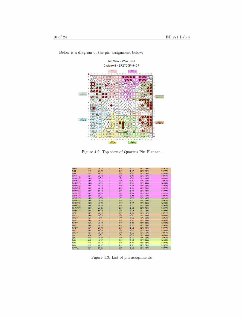
Below is a diagram of the pin assignment below:
Figure 4.2: Top view of Quartus Pin Planner.
Figure 4.3: List of pin assignments

11 of 24 EE 271 Lab 4
The three 10-Segement Bar Graph Arrays were used to visually representthe seven bit tower registers. Each anode pin was connected serially to a 1kΩresistor, and each cathode pin was grounded. The diagram of the component isbelow:
Figure 4.4: Top, side and front view of 10-segment LED array with diodes andpin assignments labeled.
5 Test Plan
5.1 Game Controller Module
Before we implement anything onto the DE1 board, we need to ensure that ourcodes first works in Bughunter, and then in the Quartus environment. However,we found out that we could not verify the schematics modules from the Quartusso our test plan is to first test the game control and ring mover modules.
In the game control module, we need to test the following conditions:
• If the user selects multiple choices for the number of rings they want, thenthe state machine goes to the error state.
• If user selects only one ring switch, then the state machine moves to thenext state.
• At a waiting state, the module waits for a done signal and only moves onto the next state when the done signal arrives.
• If the user presses one button then the machine should stay in the samestate if the user continues to press the same button. This is to preventbouncing errors.
• If the user presses one button, and then presses a different one, then themachine should output enable and wait for a done signal.

12 of 24 EE 271 Lab 4
5.2 Ring Mover Module
The ring mover called instances of Quartus built in comparator, adder andsubtracter, which restricted our ability to model the device in Bughunter. How-ever, we were still able to model the initialization of the rings and the databus.We tested all different possible initializations, which at this point are actuallylimited to only one active input since the game control module wont begininitialization if there are multiple active inputs. We also exhaustively testedmoving information from the tower registers into the choice registers via thedatabus. Our databus test was only one directional because of the symmetry ofthe databus.
Beyond this point, testing the ring mover in Bughunter is impossible becauseit wont compile Quartus schematic capture components. To test it, we used the18 LEDs available on the FPGA board. To check the state machine, we assignedthe outputs of all the flip flops to the LEDs, slowed down the clock and observedwhich states were happening. Similarly, we assigned outputs of the comparator,adder and subtracter to the LEDs to check those values as well. Obviously therearent enough LEDs to test these all at the same time so wed have to differentsets of assignments at a time.
The comparator, adder and subtracter were tested in exactly the same way.Here we will explain the test procedure for the comparator because values arecompared before they are added and subtracted so without knowing the func-tionality of the comparator, we cant efficiently test the other two parts. Theprocedures for the other two parts can be obtained by simply replacing com-parator with adder or subtracter. To test the comparator we only needed tocheck the simplest case, due to the symmetry of our design. We designed ourgame to work with any given number of rings, and because of this our design hadto be symmetric. Also, at this point we have already verified that the databusis working properly because that was tested in Bughunter. This way we knewif we could get the comparator to work once, it would always work. We usedthe LEDs to display the two seven bit inputs, and the one seven bit output ofthe comparator.
The comparator inputs just followed the selected towers, which is an easyvisual check. The output of the comparator is a one-hot binary representationof the smallest ring on the tower. For example, if the smallest ring was the thirdsmallest possible ring, the output would be 001000. Essentially, it should zeroout all terms except the smallest present ring.
The adder inputs just follow the second selected tower and the comparator.The output should be those two added together, and since the comparatoroutput was essentially just one ring, the result should be the second selectedtower, with one new ring.
Similarly, the subtracter inputs follow the first selected tower and the com-parator. The output should be the first selected tower minus the result fromthe comparator. The output should just be the first selected tower, with thefirst ring bit zeroed out.

13 of 24 EE 271 Lab 4
6 Results
6.1 Results of Game Controller
Below is an example of one set of tests completed and passed by our gamecontroller module. The test was performed in Bughunter:
Figure 6.1: Timing diagram of tests on Game Controller Module.
First we tested the error state. We input into the system multiple active ringswitches. In this case switch five and six were both active. As you can see, thesystem goes and stays in the error state until reset is hit. From here, we onlyactivate switch four, and as we expect, the machine runs until it activates enableand waits for a done signal. From here, we test the effects of bouncing. Wepress button one multiple times and observe that the state remains unchanged.We then press a different button and observe that it waits for a done signaland returns to the normal state. From here, we can pick another pair of towersto modify and check that the four bit code outputted by the game control iscorrect. In this case, we pressed buttons two and three, so we expect the outputto be 1011. We exhaustively checked that the other initializations worked, andthat the four bit codes were always what we expected.
6.2 Results of Ring Mover
Below is the timing diagram testing the first half of the ring mover module be-cause some parts of ring mover use schematic capture Verilog code from Quartuswhich does not compile in Bughunter.
First we tested staying in the reset state. We activated switch four and sentreset equal to zero. As you can see in the timing diagram, the system staysin the same state as we expected. Then the test activates enable to move onto the next state where we start loading the binary value 1 for the first fourleast significant bits of the tower1s register from the Bus giving a value of 0F inhexadecimal. Then we go back to normal state and turn on switch three only

14 of 24 EE 271 Lab 4
Figure 6.2: Timing diagram of tests on Ring Mover Module.
to test what happens when the choice bit is 0111 is inputted. As seen in thediagram the bus value gets the initial values which is 07 in hexadecimal givingthe three less significant bits in the first tower a binary value of 1 which is whatwe expected. Testing different choices of towers and initial rings in tower 1 wefind that the test results are what we expected. However, this only confirmsthat the data bus is working. To test the comparator, adder and subtracter wehad to implement the design through Quartus.
We first tested the comparator because it outputs to the adder and sub-tracter. The comparator inputs should follow the tower registers that werepicked, and by assigning those values to LEDs, we could compare them to thetower’s LED display and confirm that it wasn’t working. After some debuggingand fixing typos the comparator was following the towers, and was outputtingthe one-hot code.
Then we tested the adder and subtractor, in the same exact way we testedthe comparator. The adder should produce what the second choice should looklike after the ring has been added, and the subtractor shoud produce what thefirst choice should look like after the ring has been removed. After a long seriesof debugging and fixing, we got the adder and subtractor working.
6.3 Results of Tower of Hanoi
After testing each part individually, we integrated the system together usingthe Quartus environment and just played the game exhaustively.
7 Error Analysis
One error in this project is our extra feature. The game counter does not countthe time in order. For example, in first ten seconds, it counts as 0, 1, 2, 3, 4, 7, 9

15 of 24 EE 271 Lab 4
instead of supposedly 0, 1, 2, 3, 4, 5, 6, 7, 8, 9 and in the following, it counts as11, 12, 13, 14, 17, 18, 29, which is not in order. We think maybe the problemhas to do with some simple mistakes, like the logic equations for the D-flipflops are wrong, or a design problem. We think maybe for the tenth digit andhundredth digit on the hex display, we need to clock in with an AND gate ofthe combination of input clock and the output from the unit digit module. Forthe hundredth digit, we need to use AND gate for the input clock, tenth clock,and hundredth clock. Since we do not have these and gates to control the clockfor each module, maybe the time counter will be out of order.
8 Reasons for Incomplete Project
We did not manage to finish the extra feature, game counter due to the timeconstraints. We tried to fix it by negating the data from the GAL chip sincefirst we observed the negated hex display. However, after doing so, we noticedthat it skips some digit, like 5 and 9. Then, we tried to add the AND gate toeach clock with the data from the GAL chip. However, it still does not help. Weended up running out of time and were unable to complete the game counter.However, we still incorporated the GAL chip in our design.
9 Summary
Out of all the game projects, we chose to design and implement towers of Hanoi.We planned to design a seven ring game, meaning that user could choose thenumber of rings from one to seven. Also, we decided to use LED display tovisualize the rings to the users. As an extra feature, we put GAL chip onto theDE1 board and make it a counter. Under our test plan, it splits into both thesoftware and hardware sides. On the software side, we need to test the gamecontrol and ring mover on the bughunter pro. Then, we test all of the codesunder the Quartus. Next, we assign the pins in a way that we could determinewhich states both the game control and ring mover are in. We managed to catchseveral hundred errors when implementing our test plan. However, we did nothave time to fix the game counter as an extra feature, implemented by the GALchip.
10 Conclusion
For this lab we designed and implemented a virtual game of Tower of Hanoion the DE1 board using essentially two modules containing both sequential andcombinational logic. We also attempted to implement a counter on the GAL chipin order to display a game timer on the hexadecimal display. Using Verilog wetested the code separately and then put it all together in one big top module andprogrammed it into the DE1 board with Quartus. After exhaustively testingdifferent cases for our game functions we found out our system does exactlywhat it expected to. One error that we encountered was on the timer because

16 of 24 EE 271 Lab 4
it would not count correctly and due to time constraints we could not debugand correct Verilog code. This did not affect the functionality of our game justinconvenient for serious competitive gamers.
11 Appendix
Figure 11.1: Verilog code for Top Module.
Figure 11.2: Verilog code for Game Control pt. 1

17 of 24 EE 271 Lab 4
Figure 11.3: Verilog code for Game Control pt. 2
Figure 11.4: Verilog code for Ring Mover pt. 1.

18 of 24 EE 271 Lab 4
Figure 11.5: Verilog code for Ring Mover pt. 2.
Figure 11.6: Verilog code for Ring Mover pt. 3.

19 of 24 EE 271 Lab 4
Figure 11.7: Verilog code for Ring Mover pt. 4.
Figure 11.8: Verilog code for Ring Mover pt. 5.

20 of 24 EE 271 Lab 4
Figure 11.9: Verilog code for Ring Mover pt. 6.
Figure 11.10: Verilog code for Comparator pt. 1.

21 of 24 EE 271 Lab 4
Figure 11.11: Verilog code for Comparator pt. 2.
Figure 11.12: Verilog code for adder pt. 1.
Figure 11.13: Verilog code for adder pt. 2.

22 of 24 EE 271 Lab 4
Figure 11.14: Verilog code for parallel register pt. 1.
Figure 11.15: Verilog code for parallel register pt. 2.

23 of 24 EE 271 Lab 4
Figure 11.16: Verilog code for choice register
Figure 11.17: Timing diagram of tests on timer clock.
Figure 11.18: Timing diagram of tests on game clock.

24 of 24 EE 271 Lab 4
Figure 11.19: Verilog code for flip flop.