ee-352 ec-ii lab1
TRANSCRIPT

Electronic Circuits II Bapatla Engineering College, Bapatla.
0
ELECTRONIC CIRCUITS - II
(EE 352)
LAB MANUAL
Prepared by
Sk M SubhaniSk M SubhaniSk M SubhaniSk M Subhani
Lecturer in ECELecturer in ECELecturer in ECELecturer in ECE
T. Srinivasa RaoT. Srinivasa RaoT. Srinivasa RaoT. Srinivasa Rao
Lecturer in ECELecturer in ECELecturer in ECELecturer in ECE
DEPARTMENT OF ELECTRONICS AND COMMUNICATION ENGINEERING
BAPATLA ENGINEERING COLLEGE, BAPATLA.

Electronic Circuits II Bapatla Engineering College, Bapatla.
1
INDEX
1. Two Stage RC coupled Amplifier. 2
2. Design of voltage shunt feed back amplifier. 6
3. Clacc B push pull amplifier. 9
4. Complimentary symmetry push pull amplifier. 11
5. Design of RC phase shift oscillator. 15
6. Design of LC oscillators. 18
a.Colpitts oscillators.
b.Hartley oscillators.
7. Design of series voltage regulator. 24
8. Linear wave shaping. 29
9. Non-linear wave shaping. 34
10. Bistable multivibrator. 41
11. Monostable multivibrator. 44
12. Astable multivibrator. 47
13. Schmitt trigger. 50
14. UJT relaxation oscillator. 53
15. Blocking oscillator. 57
NOTE: A minimum of 10(Ten) experiments have to be performed and recorded by the candidate to attain eligibility for University Practical Examination.

Electronic Circuits II Bapatla Engineering College, Bapatla.
2
1. RC COUPLED AMPLIFIER
Aim: To plot the frequency response characteristics of two stages RC coupled
amplifier.
Apparatus Required:
S. No Name of the
Component/ Equipment
Specifications Quantity.
1 Two stage RC Coupled
Amplifier Circuit Board
___ 1
2 Cathode Ray Oscilloscope 20 MHz 1
3 Signal Generator 0 -1MHZ 1
4 Regulated Power Supply 0-30V,1A 1
Theory: To improve gain characteristics of an amplifier, two stages of CE amplifier can be
cascaded. While cascading, the output of one stage is connected to the input of
another stage. If R and C elements are used for coupling, that circuit is named as RC
coupled amplifier.
Each stage of the cascade amplifier should be biased at its designed level. It is
possible to design a multistage cascade in which each stage is separately biased
and coupled to the adjacent stage using blocking or coupling capacitors. In this circuit
each of the two capacitors C1 & C2 isolate the separate bias network by acting as
open circuits to dc and allow only signals of sufficient high frequency to pass through
cascade.

Electronic Circuits II Bapatla Engineering College, Bapatla.
3
Circuit Diagram:
Fig A: Two stage RC Coupled Amplifier
Procedure:
1. Connect the circuit as per the circuit diagram.
2. Apply supply voltage, Vcc= 12V.
3. Now feed an ac signal of 20mV peak-peak at the input of the amplifier
with different frequencies ranging from 20Hz to 1MHz and measure
the amplifier output voltage, Vo.
4. Now calculate the gain in dB for various input signal frequencies using
AV = 20 log10 (V0/VS).
5. Draw a graph with frequencies on X- axis and gain in dB on Y- axis.
From graph calculate bandwidth.

Electronic Circuits II Bapatla Engineering College, Bapatla.
4
Tabular Form:
Input voltage, VS = 20mV peak-peak
S. No
Input Frequency
(Hz)
Output
Voltage
peak-peak
Vo (mV)
Gain,
Av = 20log(Vo/Vs)
(dB)
Model Graph:
Observations:
Maximum gain (Av) = 52.56dB Lower cutoff frequency (Fl) = 4.5 KHz
Upper cutoff frequency (FH) =580 KHz
Band width (B.W) = (FH – FL) = 575.5 KHz
Gain bandwidth product = Av (B.W) = 30.24M Hz
Precautions:
1. Connections must be given very carefully.
2. Readings should be noted without any parallax error.
3. The applied voltage and current should not exceed the maximum ratings of
the given transistor.
Result:
Frequency response of RC Coupled Amplifier Characteristics of was observed.

Electronic Circuits II Bapatla Engineering College, Bapatla.
5
2.VOLTAGE SHUNT FEEDBACK AMPLIFIER
Aim: To plot the frequency response characteristics of voltage shunt feed back
amplifier.
Apparatus Required:
S.
No
Name of the
Component/
Equipment
Specifications Quantity.
1 Transistor BC107 1
2 Resisters 100Ω,68KΩ,8.2KΩ,,220Ω,
506Ω,1KΩ
6
3 Capacitor 10µF,47µF,10µF 3
4 Cathode Ray
Oscilloscope
20 MHz 1
5 Signal Generator 0 -1MHZ 1
6 Regulated Power
Supply
0-30V,1A 1
CIRCUIT DIAGRAM:

Electronic Circuits II Bapatla Engineering College, Bapatla.
6
MODEL WAVE FORMS
Electronic Circuits II Bapatla Engineering College, Bapatla.
7
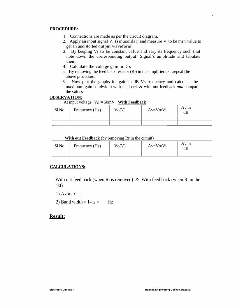
PROCEDURE:
1. Connections are made as per the circuit diagram. 2. Apply an input signal Vs (sinusoidal) and measure Vi to be min value to
get an undistorted output waveform. 3. By keeping Vi to be constant value and vary its frequency such that
note down the corresponding output! Signal’s amplitude and tabulate them.
4. Calculate the voltage gain in Db. 5. By removing the feed back resistor (Rf) in the amplifier ckt .repeal [lie
above procedure. 6. Now plot the graphs for gain in dB Vs frequency and calculate the-
maximum gain bandwidth with feedback & with out feedback and compare the values
OBSERVATION: At input voltage (Vi) = 50mV With Feedback
Sl.No. Frequency (Hz) Vo(V) Av=Vo/Vi Av in dB
With out Feedback (by removing Rr in the circuit)
Sl.No. Frequency (Hz) Vo(V) Av=Vo/Vi Av in dB
CALCULATIONS:
With out feed back (when Rf is removed) & With feed back (when Rf in the ckt)
1) Av max =
2) Band width = f2-f1 = Hz
Result:

Electronic Circuits II Bapatla Engineering College, Bapatla.
8
3.CLASS B PUSH-PULL AMPLIFIER Aim: To Design a Class B Push pull power amplifier.
Apparatus:
Sl.No Name of the Component /equipment
Specifications Qty
1 Power transistor (BD139) VCE =60V VBE = 100V IC = 100mA hfe = 40 -160
2
2 Resistor (designed values) Power rating=0.5W Carbon type
4
3 Center tap Transformers Operating temp =ambient
2
5 Function Generator 0 -1MHZ 1 6 Cathode Ray Oscilloscope 20MHZ 1 7 Regulated Power Supply 0-30V,1Amp 1
CIRCUIT DIAGRAM:
CLASS B Push-pull power amplifier

Electronic Circuits II Bapatla Engineering College, Bapatla.
9
Design Equations:
Power input: ∏= /Im2 VccPi
Power out put:
min))(2(Im/2/Im VVccVmp −== Collector citcuit
Efficiency= 100)min
1(4/)/)(4/(100)/( XVcc
VVccVmXPiP −∏=∏=
Procedure: 1. Connect the circuit as per the circuit diagram. 2. Apply input voltage and find the input power & output power. 3. Calluculate efficiency of amplifier. 4. Observe the input and output wave forms across each transistor on CRO.
Result: Class B Push-Pull power amplifier is designed &Efficiency is calculated.

Electronic Circuits II Bapatla Engineering College, Bapatla.
10
4. CLASS B COMPLEMENTARY SYMMETRY POWER AMPLIFIER
Aim:
1. Design a complementary symmetry power amplifier to deliver maximum
power to 10 Ohm load resistor.
2. Simulate the design circuit.
3. Develop the hard ware for design circuit.
4 Compare simulation results with practical results.
Apparatus:
Sl.No Name of the Component /equipment
Specifications Qty
1 Power transistor (BD139) VCE =60V VBE = 100V IC = 100mA hfe = 40 -160
1
2 Resistor (designed values) Power rating=0.5W Carbon type
4
3 Capacitors(designed values) Electrolytic type Voltage rating= 1.6v
3
4 Function Generator 0 -1MHZ 1 5 Cathode Ray Oscilloscope 20MHZ 1 6 Regulated Power Supply 0-30V,1Amp 2
Theory: In complementary symmetry class B power amplifier one is p-n-p and
other transistor is n-p-n. In the positive half cycle of input signal the transistor Q1 gets
driven into active region and starts conducting. The same signal gets applied to the
base of the Q2. it ,remains in off condition, during the positive half cycle. During the
negative half cycle of the signal the transistor Q2 p-n-p gets biased into conduction.
While Q1 gets driven into cut off region. Hence only Q2 conducts during negative half
cycle of the input, producing negative half cycle across the load.

Electronic Circuits II Bapatla Engineering College, Bapatla.
11
Circuit Diagram:
Design Equations: Given data: PL (MAX) =5 W, RL= 10Ω, f = 1KHZ
1. Selection of VCC:- PL (MAX) = VCC ² / 2RL
VCC ² = PL (MAX) 2RL = 100V VCC = 10V Selection R and RB:-
VBB = VBE = 0.6V , assume R = 150Ω VBB=VCC.R / (R+RB) 0.6 = 10*150/ (150+RB)
RB = 2.35KΩ
Capacitor calculations:-
To provide low reactances almost short circuit at the operating frequency
f=1KHZ.
XCC1 = XCC2 = (R \\ RB) / 10 = (150)(2350)/(10)(2550) = 14.1 CC1 = CC2 = 1/ 2 π f XCC1 = 11.28µF

Electronic Circuits II Bapatla Engineering College, Bapatla.
12
Procedure:
1. Connect the circuit diagram and supply the required DC supply.
2. Apply the AC signal at the input and keep the frequency at 1 KHz and
connect the power o/p meter at the output. Change the Load resistance in
steps for each value of impedance and note down the output power.
3. Plot the graph between o/p power and load impedance. From this graph
find the impedance for which the output power is maximum. This is the
value of optimum load.
4. Select load impedance which is equal to 0V or near about the optimum
load. See the wave form of the o/p of the C.R.O.
5. Calculate the power sensitivity at a maximum power o/p using the relation.
Tabular Form: Simulation: Input power = 2 VCC
2 / (πRL) = 6.36W
S.No Output Impedance(Ω) Input power (pi) (W)
Output Power(po) (W)
N=(Po)/( Pi) x100

Electronic Circuits II Bapatla Engineering College, Bapatla.
13
Practical:
Input power = 360mW
S.No Output Impedance(Ω)
Input power (pi) (mW)
Output Power(po) (mW)
N=(Po)/( Pi) x100
Model Graph:
Precautions: 1. Connections should be made care fully.
2. Take the readings with out parallax error.
3. Avoid loose connections.
4. Simulation switch must be off while changing the values.
Result: Class B complementary symmetry amplifier is designed for given specifications and its performance is observed.

Electronic Circuits II Bapatla Engineering College, Bapatla.
14
5. RC PHASE SHIFT OSCILLATOR
Aim: To determine the frequency of oscillations of an RC Phase shift oscillator.
Apparatus Required:
Theory:
In the RC phase shift oscillator, the combination RC provides self-bias for the
amplifier. The phase of the signal at the input gets reverse biased when it is amplified
by the amplifier. The output of amplifier goes to a feedback network consists of three
identical RC sections. Each RC section provides a phase shift of 600. Thus a total of
1800 phase shift is provided by the feedback network. The output of this circuit is in
the same phase as the input to the amplifier. The frequency of oscillations is given by
F=1/2π RC (6+4K)1/2 Where, R1=R2=R3=R,
C1=C2=C3=C and
K=RC/R.
S. No Name of the
Component/Equipment
Specifications Quantity
1 Transistor( BC107) Icmax=100mA PD=300mw Vceo=45V Vbeo=50V
1
2 Resistors -
56KΩ,2.2KΩ,100KΩ,10KΩ
Power rating=0.5w Carbon type
1
3
3 Capacitors 10µF/25V ,0.01µF Electrolytic type
Voltage rating=1.6v
2
3
4 Potentiometer 0-10KΩ 1
5 Regulated Power Supply 0-30V,1A 1
6 Cathode Ray Oscilloscope 20 MHz 1

Electronic Circuits II Bapatla Engineering College, Bapatla.
15
Circuit Diagram:
Fig A. RC Phase shift Oscillator
Procedure:
1. Connect the circuit as shown in Fig A.
2. Switch on the power supply.
3. Connect the CRO at the output of the circuit.
4. Adjust the RE to get undistorted waveform.
5. Measure the Amplitude and Frequency.
6. Compare the theoretical and practical values.
7. Plot the graph amplitude versus frequency
Theoretical Values:
f = 1 / 2 π RC √6+4K
=1 / 2 π (10K) (0.01µF) √6+4(0.01)
= 647.59Hz

Electronic Circuits II Bapatla Engineering College, Bapatla.
16
Tabular Form:
S.NO Theoretical
Frequency(Hz)
Practical
Frequency(Hz) % Error
Model Graph:
Result:
The frequency of RC Phase Shift Oscillator is determined.

Electronic Circuits II Bapatla Engineering College, Bapatla.
17
6A. HARTLEY OSCILLATOR
Aim:
To design a Hartley oscillator and to measure the frequency of oscillations.
Apparatus Required:
S.No Name of the
Component/Equipment
Specifications Quantity
1. Hartley Oscillator Circuit Board ___ 1
2. Cathode Ray Oscilloscope 20MHz 1
3. Decade Inductance Boxes ___ 2
Theory:
In the Hartley oscillator shown in Fig A. Z1, and Z2 are inductors and Z3 is an
capacitor. The resistors R and R2 and RE provide the necessary DC bias to the
transistor. CE is a bypass capacitor CC1 and CC2 are coupling capacitors. The
feedback network consisting of inductors L1 and L2 , Capacitor C determine the
frequency of the oscillator.
When the supply voltage +Vcc is switched ON, a transient current is produced in the
tank circuit, and consequently damped harmonic oscillations are setup in the circuit.
The current in tank circuit produces AC voltages across L1 and L2 . As terminal 3 is
earthed, it will be at zero potential.
If terminal is at positive potential with respect to 3 at any instant, then terminal 2 will
be at negative potential with respect to 3 at the same instant. Thus the phase
difference between the terminals 1 and 2 is always 1800. In the CE mode, the
transistor provides the phase difference of 1800 between the input and output.
Therefore the total phase shift is 3600. The frequency of oscillations is
f = 1/2π√LC where L= L1 + L2.

Electronic Circuits II Bapatla Engineering College, Bapatla.
18
Circuit Diagram:-
Fig A: Hartley oscillator
Procedure:
1. Switch on the power supply by inserting the power card in AC mains.
2. Connect one pair of inductors as L1 and L2 as shown in the dotted lines of
Fig A.
3. Observe the output of the oscillator on a CRO, adjust the potentiometer RE on
the front panel until we get an undistorted output. Note down the repetition
period (T) of observed signal. Compute fO = 1/T (RE can adjust the gain of the
amplifier).
4. Calculate the theoretical frequency of the circuit using the formulae.
5. Repeat the steps 2 to 4 for the second pair of inductors L1 and L2 .Tabulate
the results as below.

Electronic Circuits II Bapatla Engineering College, Bapatla.
19
Tabular Form:
S.No
Condition
Frequency , fo (KHz) % Error
Practical Theoretical
1 L1 = L2 = 100mH 3.246 3.558 8.7
2 L1 = L2 = 50mH 4.98 5.032 1
Model Graph:
Fig B: Frequency of oscillations
Precautions:
1. Connections must be done very carefully.
2. Readings should be taken without parallax error.
Result:
The frequency of Hartley oscillator is practically observed.

Electronic Circuits II Bapatla Engineering College, Bapatla.
20
6B. COLPITTS OSCILLATOR
Aim:
To measure the frequency of the Colpitts Oscillator
Apparatus Required:
S. No Name of the
Component/Equipment
Specifications Quantity
1. Colpitts Oscillator Circuit
Board
___ 1
2. Cathode Ray Oscilloscope 20 MHz 1
Theory:
In the Colpitts oscillator shown in fig 1, Z1, and Z2 are capacitors and Z3 is an
inductor. The resistors R and R2 and RE provide the necessary DC bias to the
transistor. CE is a bypass capacitor CC1 and CC2 are coupling capacitors. The
feedback network consisting of capacitors C1 and C2 , inductor L determine the
frequency of the oscillator.
When the supply voltage +Vcc is switched ON, a transient current is produced in the
tank circuit, and consequently damped harmonic oscillations are setup in the circuit.
The current in tank circuit produces AC voltages across C1 and C2 . As terminal 3 is
earthed, it will be at zero potential.
If terminal is at positive potential with respect to 3 at any instant, then terminal 2 will
be at negative potential with respect to 3 at the same instant. Thus the phase
difference between the terminals 1 and 2 is always 1800. In the CE mode, the
transistor provides the phase difference of 1800 between the input and output.
Therefore the total phase shift is 3600. The frequency of oscillations is
f = 1/2π√LC where 1/C = 1/C1 + 1/C2.

Electronic Circuits II Bapatla Engineering College, Bapatla.
21
Circuit Diagram:
Fig A: Colpitts Oscillator
Procedure:
1. Switch on the power supply by inserting the power card in AC mains
2. Connect one pair of capacitors as C1 and C2 as shown in the dotted lines of
Fig A.
3. Observe the output of the oscillator on a CRO. Adjust the potentiometer RE
on the front panel until we get an undistorted output. Note down the repetition
period (T) of observed signal. Compute fO= 1/T (RE can adjust the gain of
amplifier).
4. Calculate the theoretical frequency of the circuit using formulae.
5. Repeat the step 2 and 4 for the second pair of capacitors C1 and C2. Tabulate
the results as below.

Electronic Circuits II Bapatla Engineering College, Bapatla.
22
Tabular Form:
S.No Condition Theoretical
Frequency (KHz)
Practical
frequency(KHz) %Error
1
C1=C2=0.01µF
22.507
22.727
0.97
2
C1=C2=0.1µF
7.117
7.23
1.5
Model Graph:
Precautions:
1. Connections must be done very carefully.
2. Readings should be taken without parallax error.
Result:
The frequency of Colpitts Oscillators is practically determined.

Electronic Circuits II Bapatla Engineering College, Bapatla.
23
7. SERIES VOLTAGE REGULATOR Aim:
1. Design series voltage regulator to operate on supply of 15v.
2. Simulate the design of regulator.
3. Develop the hardware for design of voltage regulator.
4. Compare the practical results with theoretical results.
Apparatus:
S.No Name of the component/equipment
Specifications Qty
1
Zener diode (Bz6.5) Vz=6.5v 1
2 Transistors (BC 107)
I c max =100ma, VCEO =45v, Pd(min) =300mw
1
3 Resistors(designed values) Power dissipation=0.5w Carbon type Tolerance ±5%
1
4 Regulated power supply 0-30 V,1Amp 1
Theory: A regulator is an electronic circuit which maintains a constant output
irrespective of change in input voltage, load resistance and change in temperature.
Series voltage regulator is one type of regulator. If in a voltage regulator circuit , the
control element is connected in series with the load ,then the circuit is called series
voltage regulator circuit. The unregulated d.c voltage is the input to the circuit. The
control element controls the input voltage, that gets to the output. The sampling
circuit provides the necessary feed back signal. The comparator circuit compares the
feed back with the reference voltage to generate appropriate control signal. In a
transistorized series feedback type regulator the output voltage is given by Vo = (1+R1/R2) (VBE2+Vz)

Electronic Circuits II Bapatla Engineering College, Bapatla.
24
Circuit Diagram:
Design Equations: Given data: VL= 9V, IL = 40mA, IZ = 1mA, VZ = 6.5V Vi =15V, IB =1mA, hfe=100
1. Assume the current flowing through the resistor R1 & R3 is 1/10 of the IL I1=I3=IL/10 =40mA / 10 = 4mA
2. IE1=I1+I3+IL = 48mA
3. RL=VL/IL = 9/(40 X 10-3) = 225Ω 4. VO=VL=R3I3+VZ
R3=VL-VZ/I3 = 375Ω 5. R1I1+VBE2+VZ=VO R1=VO-(VBE2+VZ)/I1 = 220Ω 4 R2I2 = VBE2 + VZ
R2 = 2.04KΩ
hfe = 100, IC2 = 3mA
5 I2 = I1-IB2 ( Since hfe = IC2/IB2 ) I2= 3.97mA
6 I4= IB1 + IC2 IB1 = IC1 / hfe1 (IC1 = IE1) I4 = 3.48mA
7 Vi = I4R4 + VBE1 + VO R4 = 2.98KΩ

Electronic Circuits II Bapatla Engineering College, Bapatla.
25
Procedure:
1. Connect the Circuit diagram as shown in the fig:
2. Apply the input voltage of 15V
3. Keep the input Voltage constant. Vary the load resistance and measure the
output Voltage and output current
4. Tabulate the readings
5. Plot the graph between Load current versus Load Resistance and Output
Voltage versus Load resistance.
Tabular forms: Simulation:
S.No Load resistance RL (Ohms)
Output Voltage (v) Output Current IL (mA)

Electronic Circuits II Bapatla Engineering College, Bapatla.
26
Practical
S.No Load resistance (RL in Ohms)
o/p voltage (v)
o/p current IL (mA)

Electronic Circuits II Bapatla Engineering College, Bapatla.
27
Model graph:
Precautions:
1. Connections should me made care fully.
2. Take the readings with out parallax error.
Result: A series voltage regulator of 9V output is designed and verified.

Electronic Circuits II Bapatla Engineering College, Bapatla.
28
8. Linear Wave Shaping
Aim:
i) To design a low pass RC circuit for the given cutoff frequency and obtain its
frequency response.
ii) To observe the response of the designed low pass RC circuit for the given
square waveform for T<<RC,T=RC and T>>RC.
iii) To design a high pass RC circuit for the given cutoff frequency and obtain
its frequency response.
iv) To observe the response of the designed high pass RC circuit for the given
square waveform for T<<RC, T=RC and T>>RC.
Apparatus Required:
Name of the
Component/Equipment
Specifications Quantity
Resistors 1KΩ 1
2.2KΩ,16 KΩ 1
Capacitors 0.01µF 1
CRO 20MHz 1
Function generator 1MHz 1
Theory:
The process whereby the form of a non sinusoidal signal is altered by
transmission through a linear network is called “linear wave shaping”. An ideal
low pass circuit is one that allows all the input frequencies below a frequency
called cutoff frequency fc and attenuates all those above this frequency. For
practical low pass circuit (Fig.1) cutoff is set to occur at a frequency where the
gain of the circuit falls by 3 dB from its maximum at very high frequencies the
capacitive reactance is very small, so the output is almost equal to the input and
hence the gain is equal to 1. Since circuit attenuates low frequency signals and
allows high frequency signals with little or no attenuation, it is called a high pass
circuit.

Electronic Circuits II Bapatla Engineering College, Bapatla.
29
Circuit Diagram:
Low Pass RC Circuit :
High Pass RC Circuit :
Procedure:
A) Frequency response characteristics:
1 .Connect the circuit as shown in Fig.1 and apply a sinusoidal signal of
amplitude of 2V p-p as input.
2. Vary the frequency of input signal in suitable steps 100 Hz to 1 MHz and note
down the p-p amplitude of output signal.
3. Obtain frequency response characteristics of the circuit by finding gain at each
frequency and plotting gain in dB vs frequency.
4. Find the cutoff frequency fc by noting the value of f at 3 dB down from the
maximum gain

Electronic Circuits II Bapatla Engineering College, Bapatla.
30
B) Response of the circuit for different time constants:
Time constant of the circuit RC= 0.0198 ms
1. Apply a square wave of 2v p-p amplitude as input.
2. Adjust the time period of the waveform so that T>>RC, T=RC,T<<RC and
observe the output in each case.
3. Draw the input and output wave forms for different cases.
Sample readings
Low Pass RC Circuit
Input Voltage: Vi=2 V(p-p)
S.No Frequency
(Hz)
O/P Voltage, Vo
(V)
Gain = 20log(Vo/Vi)
(dB)
High Pass RC Circuit:
S.No Frequency
(Hz)
O/P Voltage, Vo
(V)
Gain = 20log(Vo/Vi)
(dB)
Model Graphs and wave forms
Low Pass RC circuit frequency response:
High Pass RC circuit frequency response:

Electronic Circuits II Bapatla Engineering College, Bapatla.
31
Low Pass RC circuit

Electronic Circuits II Bapatla Engineering College, Bapatla.
32
High Pass RC Circuit
Precautions:
1. Connections should be made carefully.
2. Verify the circuit connections before giving supply.
3. Take readings without any parallax error.
Result:
RC low pass and high pass circuits are designed, frequency response and
response at different time constants is observed.

Electronic Circuits II Bapatla Engineering College, Bapatla.
33
9. Non Linear Wave Shaping-Clippers
Aim: To obtain the output and transfer characteristics of various diode clipper
circuits.
Apparatus required:
Name of the
Component/Equipment Specifications Quantity
Resistors 1KΩ 1
Diode 1N4007 1
Cathode Ray Oscilloscope 20MHz 1
Function generator 1MHz 1
Regulated power supply 0-30V,1A 1
Theory:
The basic action of a clipper circuit is to remove certain portions of the
waveform, above or below certain levels as per the requirements. Thus the circuits
which are used to clip off unwanted portion of the waveform, without distorting the
remaining part of the waveform are called clipper circuits or Clippers. The half wave
rectifier is the best and simplest type of clipper circuit which clips off the
positive/negative portion of the input signal. The clipper circuits are also called limiters
or slicers.
Circuit diagrams:
Positive peak clipper with reference voltage, V=2V

Electronic Circuits II Bapatla Engineering College, Bapatla.
34
Positive Base Clipper with Reference Voltage, V=2V
Negative Base Clipper with Reference Voltage,V=-2V
Negative peak clipper with reference voltage, V=-2v

Electronic Circuits II Bapatla Engineering College, Bapatla.
35
Slicer Circuit:
Procedure:
1. Connect the circuit as per circuit diagram shown in Fig.1
2. Obtain a sine wave of constant amplitude 8 V p-p from function generator and
apply as input to the circuit.
3. Observe the output waveform and note down the amplitude at which clipping
occurs.
4. Draw the observed output waveforms.
5 . To obtain the transfer characteristics apply dc voltage at input terminals and
vary the voltage insteps of 1V up to the voltage level more than the reference
voltage and note down the corresponding voltages at the output.
6 . Plot the transfer characteristics between output and input voltages.
7. Repeat the steps 1 to 5 for all other circuits.
Sample Readings:
Positive peak clipper: Reference voltage, V=2V
S.No I/p voltage
(v)
O/p voltage
(v)
Positive base clipper: Reference voltage V= 2V
S.No I/p voltage(v) O/p voltage(v)

Electronic Circuits II Bapatla Engineering College, Bapatla.
36
Negative base clipper: Reference voltage= 2V
Negative peak clipper: Reference voltage= 2 V
Slicer Circuit:
Theoretical calculations:
Positive peak clipper:
Vr=2v, Vγ=0.6v
When the diode is forward biased Vo =Vr+ Vγ
=2v+0.6v
= 2.6v
When the diode is reverse biased the Vo=Vi
Positive base clipper:
Vr=2v, Vγ=0.6v
When the diode is forward biased Vo=Vr –Vγ
= 2v-0.6v
= 1.4v
When the diode is reverse biased Vo=Vi .
Negative base clipper:
Vr=2v, Vγ=0.6v
S.No I/p voltage(v) O/p voltage(v)
S.No I/p voltage(v) O/p voltage(v)
S.No I/p voltage(v) O/p voltage(v)

Electronic Circuits II Bapatla Engineering College, Bapatla.
37
When the diode is forward biased Vo = -Vr+ Vγ
=-2v+0.6v
=-1.4v
When the diode is reverse biased Vo=Vi .
Negative peak clipper:
Vr=2v, Vγ=0.6v
When the diode is forward biased Vo= -(Vr+ Vγ)
= -(2+0.6)v
=-2.6v
When the diode is reverse biased Vo=Vi .
Slicer:
When the diode D1 is forward biased and D2 is reverse biased Vo= Vr+ Vγ
=2.6v
When the diode D2 is forward biased and D2 is reverse biased Vo=-(Vr+ Vγ)
= -(2+0.6)v
=-2.6v
When the diodes D1 &D2 are reverse biased Vo=Vi .
Model wave forms and Transfer characteristics
Positive peak clipper: Reference voltage= 2V

Electronic Circuits II Bapatla Engineering College, Bapatla.
38
Positive base clipper: Reference voltage= 2V
Negative base clipper: Reference voltage= 2v
Negative peak clipper: Reference voltage= 2 V

Electronic Circuits II Bapatla Engineering College, Bapatla.
39
Slicer Circuit:
Precautions:
1. Connections should be made carefully.
2. Verify the circuit before giving supply.
3. Take readings without any parallax error.
Result:
Performance of different clipping circuits is observed and their transfer characteristics
are obtained.

Electronic Circuits II Bapatla Engineering College, Bapatla.
40
10. BISTABLE MULTIVIBRATOR
Aim: To Observe the stable states voltages of Bistable Multivibrator.
Apparatus required:
Name of the
Component/Equipment
Specifications Quantity
Transistor BC 107 2
Resistors 2.2KΩ 2
12KΩ 2
Regulated Power Supply 0-30V, 1A 1
Theory:
The circuit diagram of a fixed bias bistable multivibrator using transistors. The output of
each amplifier is direct coupled to the input of the other amplifier. In one of the stable
states transistor Q1 and Q2 is off and in the other stable state. Q1 is off and Q2 is on even
though the circuit is symmetrical; it is not possible for the circuit to remain in a stable
state with both the transistors conducting simultaneously and caring equal currents. The
reason is that if we assume that both the transistors are biased equally and are carrying
equal currents i1 and i2 suppose there is a minute fluctuation in the current i1-let us say it
increases by a small amount .Then the voltage at the collector of q1 decreases. This will
result in a decrease in voltage at the base of q2. So q2 conducts less and i2 decreases
and hence the potential at the collector of q2 increases. This results in an increase in the
base potential of q1.So q1 conducts still more and i1 is further increased and the potential
at the collector of q1 is further decreased, and so on . So the current i1 keeps on
increasing and the current i2 keeps on decreasing till q1 goes in to saturation and q2 goes
in to cut-off. This action takes place because of the regenerative feed –back incorporated
into the circuit and will occur only if the loop gain is greater than one.

Electronic Circuits II Bapatla Engineering College, Bapatla.
41
Circuit Diagram:
Procedure:
1. Connect the circuit as shown in figure.
2. Verify the stable state by measuring the voltages at two collectors by using
multimeter.
3. Note down the corresponding base voltages of the same state (say state-1).
4. To change the state, apply negative voltage (say-2v) to the base of on
transistor or positive voltage to the base of transistor (through proper
current limiting resistance).
5. Verify the state by measuring voltages at collector and also note down
voltages at each base.
Observations :
Sample Readings
Before Triggering
Q1(OFF) Q1(ON)
VBE1=0.03V VBE2=0.65V
VCE1=5.6V VCE2=0.03V
After Triggering
Q1(ON) Q1(OFF)
VBE1=0.65V VBE2=0.01V
VCE1=0.03V VCE2=5.6V

Electronic Circuits II Bapatla Engineering College, Bapatla.
42
Precautions:
1. Connections should be made carefully.
2. Note down the parameters carefully.
3. The supply voltage levels should not exceed the maximum rating of the transistor.
Result: The stable state voltages of a bistable multivibrator are observed.

Electronic Circuits II Bapatla Engineering College, Bapatla.
43
11. MONOSTABLE MULTIVIBRATOR
Aim: To observe the stable state and quasi stable state voltages in monostable
multivibrator.
Apparatus Required:
Name of the
Component/Equipment Specifications Quantity
Transistor (BC 107) 2
Resistors
1.5KΩ 1
2.2KΩ 2
68KΩ 1
1KΩ 1
Capacitor 1µF 2
Diode 0A79 1
CRO 20MHz 1
Function generator 1MHz 1
Regulated Power
Supply 0-30V, 1A
1
Theory:
A monostable multivibrator on the other hand compared to astable, bistable has only one
stable state, the other state being quasi stable state. Normally the multivibrator is in
stable state and when an externally triggering pulse is applied, it switches from the stable
to the quasi stable state. It remains in the quasi stable state for a short duration, but
automatically reverse switches back to its origional stable state without any triggering
pulse.The monostable multivibrator is also referred as ‘one shot’ or ‘uni vibrator’ since
only one triggering signal is required to reverse the original stable state. The duration of
quasi stable state is termed as delay time (or) pulse width (or) gate time.It is denoted
as ‘t’.

Electronic Circuits II Bapatla Engineering College, Bapatla.
44
CCCiiirrrcccuuuiiittt DDDiiiaaagggrrraaammm:::
Procedure:
1. Connect the circuit as per the circuit diagram.
2. Verify the stable states of Q1 and Q2
3. Apply the square wave of 2v p-p , 1KHz signal to the trigger circuit.
4 Observe the wave forms at base of each transistor simultaneously.
5. Observe the wave forms at collectors of each transistors simultaneously.
6.. Note down the parameters carefully.
7 Note down the time period and compare it with theoretical values.
8. Plot wave forms of Vb1, Vb2,Vc1 & Vc2 with respect to time .
Calculations:
Theoretical Values:
Time Period, T = 0.693RC
= 0.693x68x103x0.01x10-6
= 47µ sec
= 0.047 m sec
Frequency, f = 1/T = 21 kHz

Electronic Circuits II Bapatla Engineering College, Bapatla.
45
Model waveforms:
Precautions:
1. Connections should be made carefully.
2. Note down the parameters without parallax error.
3. The supply voltage levels should not exceed the maximum rating of the transistor.
Result:
Stable state and quasi stable state voltages in monostable multivibrator are observed

Electronic Circuits II Bapatla Engineering College, Bapatla.
46
12. ASTABLE MULTIVIBRATOR
Aim: To Observe the ON & OFF states of Transistor in an Astable Multivibrator.
Apparatus required:
Name of the
Component/Equipment
Specifications Quantity
Transistor (BC 107) BC 107 2
Resistors 3.9KΩ 2
100KΩ 2
Capacitor 0.01µF 2
Regulated Power Supply 0-30V, 1A 1
Theory :.
An Astable Multivibrator has two quasi stable states and it keeps on switching
between these two states by itself . No external triggering signal is needed . The
astable multivibrator cannot remain indefinitely in any one of the two states .The
two amplifier stages of an astable multivibrator are regenerative across coupled by
capacitors. The astable multivibrator may be to generate a square wave of
period,1.38RC.
Circuit Diagram

Electronic Circuits II Bapatla Engineering College, Bapatla.
47
Procedure :
1. Calculate the theoratical frequency of oscillations of the circuit.
2.Connect the circuit as per the circuit diagram.
3 Observe the voltage wave forms at both collectors of two transistors
simultaneously.
4. Observe the voltage wave forms at each base simultaneously with
corresponding collector voltage.
5. Note down the values of wave forms carefully.
6. Compare the theoratical and practical values.
Calculations:
Theoritical Values :
RC= R1C1+ R2C2
Time Period, T = 1.368RC
= 1.368x100x103x0.01x10-6
= 93 µ sec
= 0.093 m sec
Frequency, f = 1/T = 10.75kHz

Electronic Circuits II Bapatla Engineering College, Bapatla.
48
Model waveforms :
Precautions :
1. Connections should be made carefully.
2. Readings should be noted without parallax error.
Result :
The wave forms of astable multivibrator has been verified.

Electronic Circuits II Bapatla Engineering College, Bapatla.
49
13.SCHMITT TRIGGER
Aim: To Generate a square wave from a given sine wave using Schmitt Trigger
Apparatus Required:
Theory:
Schmitt trigger is a bistable circuit and the existence of only two stable states results
form the fact that positive feedback is incorporated into the circuit and from the further
fact that the loop gain of the circuit is greater than unity. There are several ways to
adjust the loop gain. One way of adjusting the loop gain is by varying Rc1. Under
quiescent conditions Q1 is OFF and Q2 is ON because it gets the required base drive
from Vcc through Rc1 and R1. So the output voltage is Vo=Vcc-Ic2Rc2 is at its lower
level. Untill then the output remains at its lower level.
Name of the
Component/Equipment
Values/Specifications Quantity
Transistor BC 107 2
Resistors
100Ω 1
6.8KΩ 1
3.9KΩ 1
2.7KΩ 1
2.2KΩ 1
Capacitor 0.01µF 1
CRO 20MHz 1
Regulated Power Supply 30V 1
Function generator 1MHz 1

Electronic Circuits II Bapatla Engineering College, Bapatla.
50
Circuit diagram :
Procedure:
1 Connect the circuit as per circuit diagram.
2 Apply a sine wave of peak to peak amplitude 10V, 1 KHz frequency wave as input to
the circuit.
3 Observe input and output waveforms simultaneously in channel 1 and channel 2 of
CRO.
4 Note down the input voltage levels at which output changes the voltage level.
5 Draw the graph between votage versus time of input and output signals.

Electronic Circuits II Bapatla Engineering College, Bapatla.
51
Model Graph:
Precautions:
1. Connections should be made carefully.
2. Readings should be noted carefully without any parallax error.
Result: Schmitt trigger is constructed and observed its performance.
Inference:
Schmitt trigger circuit is a emitter coupled bistable circuit, and existence of only
two stable states results from the fact that positive feedback is incorporated into the
circuit, and from the further fact that the loop gain of the circuit is greater than unity.
Question & Answers:
1. What is the other name of the Schmitt trigger?
Ans Emitter coupled Binary
2. What are the applications of the Schmitt trigger?
Ans Amplitude Comparator, Squaring circuit
3. Define the terms UTP & LTP?
Ans. UTP is defined as the input voltage at which Q1 starts conducting, LTP is
defined as the input voltage at which Q2 resumes conduction.

Electronic Circuits II Bapatla Engineering College, Bapatla.
52
14. UJT RELAXATION OSCILLATOR
Aim: To obtain the characteristics of UJT Relaxation Oscillator.
Apparatus Required:
Name of the
Component/Equipment
Specifications Quantity
UJT 2N 2646 1
Resistors
220Ω 1
68KΩ 1
120Ω 1
Capacitor
0.1µF 1
0.01µF 1
0.001µF 1
Diode 0A79 1
Inductor 130mH 1
CRO 20MHz 1
Function generator 1MHz 1
Regulated Power Supply (0-30V),1A 1
Theory:
Many devices such as transistor,UJT, FET can be used as a switch. Here UJT is used as
a switch to obtain the sweep voltage. Capacitor C charges through the resistor,R
towards supply Voltage,Vbb. As long as the capacitor voltage is less than peak
Voltage,Vp, the emitter appears as an open circuit.
Vp =ηVbb + Vγ where,η = stand off ratio of UJT,
Vγ = Cut in voltage of diode.
When the voltage Vo exceeds voltage Vp, the UJT fires. The Capacitor starts discharging
through R1 + Rb1. Where, Rb1 is the internal base resistance. This process is repeated
until the power supply is available.

Electronic Circuits II Bapatla Engineering College, Bapatla.
53
Circuit diagram:
Design equations:
Theoretical Calculations:
Vp = Vγ+(R1/ R1 R2 )Vbb
=0.7+(120/120+220)10
=8.57V
1. When C=0.1µF
Tc =RC ln(Vbb- Vv/ Vbb- Vp)
=(68K) (0.1µF) (12/12-8.57)
= 3.6ms
Td =R1C=(120)( 0.1µ)=12 µsec.
2. When C=0.01µF
Tc =RC ln(Vbb- Vv/ Vbb- Vp)
=(68K) (0.01µF) (12/12-8.5)
= 365µs

Electronic Circuits II Bapatla Engineering College, Bapatla.
54
Td =R1C=(120)( 0.01µ)=1.2 µsec.
3. When C=0.001µF
Tc =RC ln(Vbb- Vv/ Vbb- Vp)
=(68K) (0.001µF) (12/12-8.5)
= 36.5µs
Td =R1C=(120)( 0.01µ)=0.12 µsec
S.NO Capacitance value
(µF)
Theoretical time
period
Practical time
period
Procedure:
1) Connect the circuit as shown in figA.
2) Observe the voltage waveform across the capacitor,C.
3) Change the time constant by changing the capacitor values to 0.1µF and 0.001 µF
and observe the wave forms.
4) Note down the parameters, amplitude,charging and discharging periods of the wave
forms
5)Compare the theoretical and practical time periods.
6)Plot the graph between voltage across capacitor with respect to time
Model graph:

Electronic Circuits II Bapatla Engineering College, Bapatla.
55
Precautions:
1.Connections should be given carefully.
2. Readings should be noted without parallox error.
Result:
Performance and construction of UJT Relaxation Oscillator is observed.

Electronic Circuits II Bapatla Engineering College, Bapatla.
56
15.Blocking oscillator
Aim: To obtain the characteristics of Blocking Oscillator.
Apparatus Required:
Name of the
Component/Equipment
Specifications Quantity
transfotmer 1
Resistors 220Ω 1
Capacitor 0.1µF 1
Transistor NPN 1
CRO 20MHz 1
Function generator 1MHz 1
Regulated Power Supply (0-30V),1A 1
Theory:
A blocking oscillator is the minimal configuration of discrete electronic
Components which can produce a free-running signal, requiring only
a capacitor, transformer, and one amplifying component. The name is
Derived from the fact that the transistor (or tube) is cut-off or
"blocked" for most of the duty-cycle, producing periodic pulses. The
Non-sinusoidal output is not suitable for use as a radio-frequency
Local oscillator, but it can serve to flash lights or LEDs, and the
simple tones are sufficient for applications such as alarms or a morse-
code practice device. Some cameras use a blocking oscillator to strobe
the flash prior to a shot to reduce the red-eye effect.

Electronic Circuits II Bapatla Engineering College, Bapatla.
57
.
Due to the simplicity of the circuit, it forms the basis for many of the
learning projects in commercial electronic kits. A secondary winding of
the transformer can be fed to a speaker, a lamp, or the windings of a
relay. A potentiometer placed in parallel with the timing capacitor
permits the frequency to be adjusted, but at low resistances the
transistor will be overdriven, and possibly damaged. The output signal
will jump in amplitude and be greatly distorted. The frequency of the
oscillator is also affected by the supply voltage
Circuit diagram:
Model graph:
Blocking oscillator out put wave form

Electronic Circuits II Bapatla Engineering College, Bapatla.
58
Procedure:
1) Connect the circuit as per the circuit diagram.
2) Observe the voltage waveform across the collector of transistor..
3) Change the time constant by changing the capacitor values to 0.1µF and 0.001 µF
and observe the wave forms.
4) Note down the parameters, amplitude,charging and discharging periods of the wave
forms
Result:
Study of blocking oscillator is done.
----------------------------------------------------------------------------------------------------------

Electronic Circuits II Bapatla Engineering College, Bapatla.
59

Electronic Circuits II Bapatla Engineering College, Bapatla.
60