ee141 © digital integrated circuits 2nd manufacturing 1 manufacturing process i dr. shiyan hu...
TRANSCRIPT

EE141© Digital Integrated Circuits2nd Manufacturing1
ManufacturingManufacturingProcess IProcess I
Dr. Shiyan HuOffice: EERC 518
Adapted and modified from Digital Integrated Circuits: A Design Perspective by Jan M. Rabaey, Anantha Chandrakasan, and Borivoje Nikolic.
EE4271EE4271VLSI DesignVLSI Design

EE141© Digital Integrated Circuits2nd Manufacturing2
Silicon WaferSilicon Wafer
Single die
Wafer
From http://www.amd.com
Going up to 12” (30cm)

EE141© Digital Integrated Circuits2nd Manufacturing3
N-Well ProcessN-Well Process

EE141© Digital Integrated Circuits2nd Manufacturing4
Dual-Well ProcessDual-Well Process
p-well n-well
p+
p-epi
SiO2
AlCu
poly
n+
SiO2
p+
gate-oxide
Tungsten
TiSi2
Dual-Well Trench-Isolated CMOS ProcessDual-Well Trench-Isolated CMOS Process
Transistors at bottom
Wires on the top

EE141© Digital Integrated Circuits2nd Manufacturing5
Circuit Under DesignCircuit Under Design
VDD VDD
VinVout
M1
M2
M3
M4
Vout2

EE141© Digital Integrated Circuits2nd Manufacturing6
Its Layout ViewIts Layout View

EE141© Digital Integrated Circuits2nd Manufacturing77
VLSI Design and FabricationVLSI Design and Fabrication
Lithography Process
Designed Chip Layout
Fabricated Chip

EE141© Digital Integrated Circuits2nd Manufacturing8
ChipChip

EE141© Digital Integrated Circuits2nd Manufacturing99
Lithography System - Simple ViewLithography System - Simple View
Illumination source
Mask
Objective Lens
Aperture
Wafer

EE141© Digital Integrated Circuits2nd Manufacturing1010
Photo-Lithography Process – Full ViewPhoto-Lithography Process – Full View
oxidation
opticalmask
processstep
photoresist coatingphotoresistremoval (ashing)
spin, rinse, dryacid etch
photoresist
stepper exposure
development
Typical operations in a single photolithographic cycle (from [Fullman]).
Part of layout

EE141© Digital Integrated Circuits2nd Manufacturing11
An Example: Patterning of SiO2An Example: Patterning of SiO2
Si-substrate
Si-substrate Si-substrate
(a) Silicon base material
(b) After oxidation and depositionof negative photoresist
(c) Stepper exposure
PhotoresistSiO2
UV-light
Patternedoptical mask
Exposed resist
SiO2
Si-substrate
Si-substrate
Si-substrate
SiO2
SiO2
(d) After development and etching of resist,chemical or plasma etch of SiO2
(e) After etching
(f) Final result after removal of resist
Hardened resist
Hardened resist
Chemical or plasmaetch

EE141© Digital Integrated Circuits2nd Manufacturing
Manufacturing ProcessManufacturing Process
12
Part of the layout is put on a mask (level), so we have many masks.
Each mask level corresponds to different actions in the fabrication process
Each mask level contains non-overlapping polygons, but polygons from different masks may overlap
EE141© Digital Integrated Circuits2nd Manufacturing
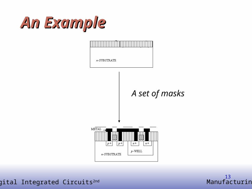
An Example An Example
13
A set of masks

EE141© Digital Integrated Circuits2nd Manufacturing
An Example - IAn Example - I
14

EE141© Digital Integrated Circuits2nd Manufacturing
An Example - IIAn Example - II
15

EE141© Digital Integrated Circuits2nd Manufacturing
An Example - IIIAn Example - III
16

EE141© Digital Integrated Circuits2nd Manufacturing
An Example - IVAn Example - IV
17

EE141© Digital Integrated Circuits2nd Manufacturing
An Example - VAn Example - V
18

EE141© Digital Integrated Circuits2nd Manufacturing
An Example - VIAn Example - VI
19
Active (diffusion) contact
Insulator SiO2 for building metals in next step

EE141© Digital Integrated Circuits2nd Manufacturing
An Example - VIIAn Example - VII
20

EE141© Digital Integrated Circuits2nd Manufacturing21
General CMOS ProcessGeneral CMOS ProcessDefine active areasEtch and fill trenches
Implant well regions
Deposit and patternpolysilicon layer
Implant source and drainregions and substrate contacts
Create contact and via windowsDeposit and pattern metal layers

EE141© Digital Integrated Circuits2nd Manufacturing22
Contact and ViaContact and Via
Contact: link metal with diffusion (active) Link metal with gate poly
Via: Link wire with wire
Overlapping two layers (diffusion, gate poly or metal) and providing a contact hole filled with metal
Substrate Contact and Well Contact: Link substrate or well to supply voltage

EE141© Digital Integrated Circuits2nd Manufacturing23
CMOS Process Walk-ThroughCMOS Process Walk-Through
p+
p-epi (a) Base material: p+ substrate with p-epi layer (extended layer)
p+
(c) After plasma etch of insulatingtrenches using the inverse of the active area mask
p+
p-epiSiO2
3SiN
4
(b) After deposition of gate-oxide andsacrificial nitride (acts as abuffer layer)

EE141© Digital Integrated Circuits2nd Manufacturing24
CMOS Process Walk-ThroughCMOS Process Walk-ThroughSiO (field oxide)2
(d) After trench filling, CMP planarization, and removal of sacrificial nitride
(e) After n-well implants (by adjusting well doping in order to have more donar impurities such as phosphorus)
n
(f) After p-well implants(by adjusting well doping in order to have more acceptor impurities such as boron)
p
This implant will only impact the area below the gate oxide but not gate oxide itself

EE141© Digital Integrated Circuits2nd Manufacturing25
CMOS Process Walk-ThroughCMOS Process Walk-Through
(g) After polysilicon depositionand etch
poly(silicon)
(h) After n+ source/drain andp+ source/drain implants.
p+n+
(i) After deposition of SiO2insulator and contact hole etch.
SiO2

EE141© Digital Integrated Circuits2nd Manufacturing26
CMOS Process Walk-ThroughCMOS Process Walk-Through
(j) After deposition and patterning of first Al metallayer.
Al
(k) After deposition of SiO2insulator, etching of via’s,
deposition and patterning ofsecond metal layer of Al.
AlSiO2

EE141© Digital Integrated Circuits2nd Manufacturing27
CMOSCMOS
Polysilicon Aluminum

EE141© Digital Integrated Circuits2nd Manufacturing28
MetalMetal