ee141 system-on-chip test architectures ch. 14 – high-speed i/o interface - p. 1 1 chapter 14...
TRANSCRIPT
EE141System-on-Chip Test Architectures Ch. 14 – High-Speed I/O Interface - P. 11
Chapter 14Chapter 14
High-Speed I/O InterfaceHigh-Speed I/O Interface
EE141System-on-Chip Test Architectures Ch. 14 – High-Speed I/O Interface - P. 22
What is this chapter about?What is this chapter about? High-speed I/O interfacesHigh-speed I/O interfaces
Have been widely used in computer, communication, and consumer electronics systems
Are able to transmit and receive data at higher rates with fewer I/O pins
Focus on High-speed I/O architectures I/O interface testing
At the Component/subsystem levelAt the System levelUsing DFT-assisted Methods
New challenges in high-speed I/O and testing
EE141System-on-Chip Test Architectures Ch. 14 – High-Speed I/O Interface - P. 33
OutlineOutlineI. High-Speed I/O Architectures
Global Clock I/O Architectures Source Synchronous I/O Architectures Embedded Clock I/O Architectures Basics on Jitter, Noise, and Bit Error Rate (BER)
II. Testing of I/O Interfaces Testing of Global Clock I/O Testing of Source Synchronous I/O Testing of Embedded Clock High-Speed Serial I/O
III. DFT-Assisted Testing AC Loopback Testing High-Speed Serial-Link Loopback Testing Testing the Equalizers
IV. System-Level Interconnect Testing Interconnect Testing with Boundary Scan Interconnect Testing with High-Speed Boundary Scan Interconnect Built-In Self-Test
V. Future Challenges
VI. Concluding Remarks
EE141System-on-Chip Test Architectures Ch. 14 – High-Speed I/O Interface - P. 44
I. High-Speed I/O ArchitecturesI. High-Speed I/O Architectures
EE141System-on-Chip Test Architectures Ch. 14 – High-Speed I/O Interface - P. 55
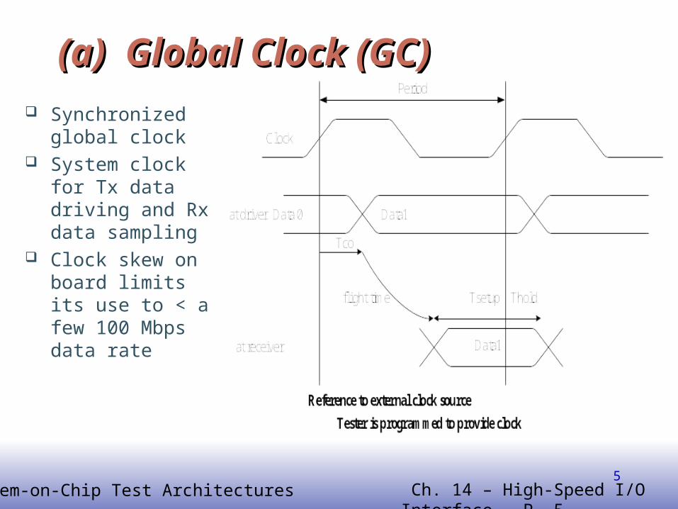
(a) Global Clock (GC)(a) Global Clock (GC) Synchronized global
clock System clock for Tx
data driving and Rx data sampling
Clock skew on board limits its use to < a few 100 Mbps data rate
EE141System-on-Chip Test Architectures Ch. 14 – High-Speed I/O Interface - P. 66
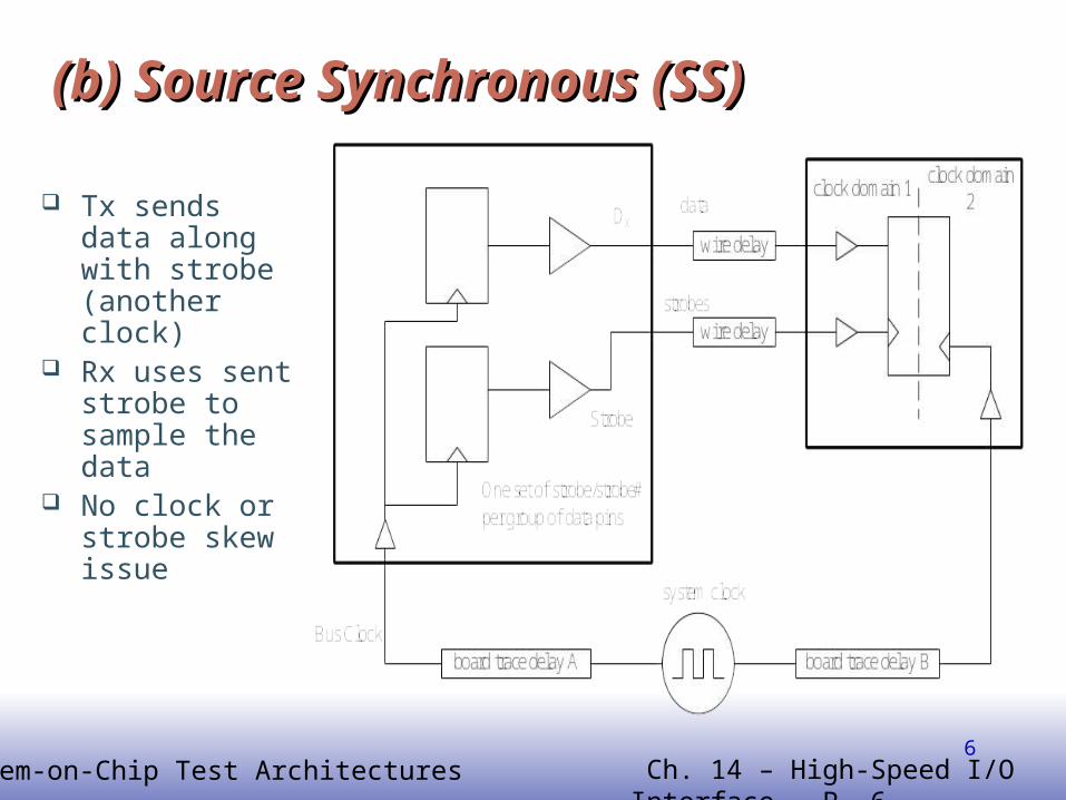
(b) Source Synchronous (SS)(b) Source Synchronous (SS)
Tx sends data along with strobe (another clock)
Rx uses sent strobe to sample the data
No clock or strobe skew issue
EE141System-on-Chip Test Architectures Ch. 14 – High-Speed I/O Interface - P. 77
Source Synchronous (SS) (Cont’d)Source Synchronous (SS) (Cont’d)
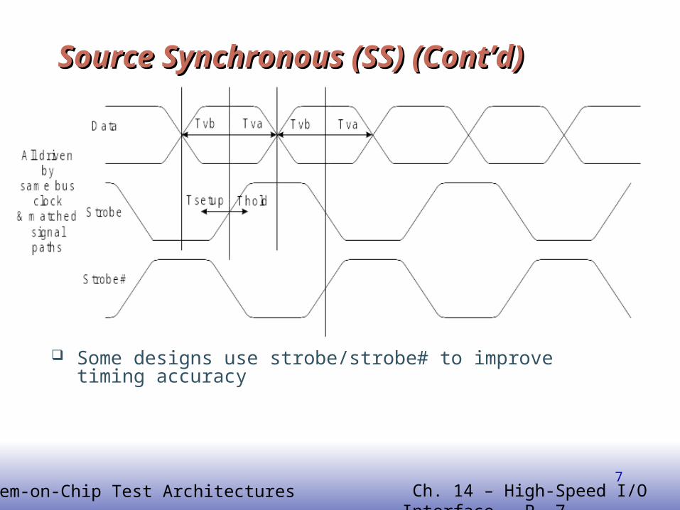
Some designs use strobe/strobe# to improve timing accuracy
EE141System-on-Chip Test Architectures Ch. 14 – High-Speed I/O Interface - P. 88
Source Synchronous (SS) (Cont’d)Source Synchronous (SS) (Cont’d)
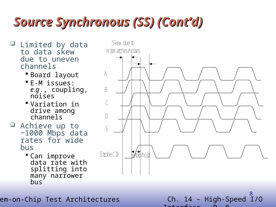
Limited by data to data skew due to uneven channels Board layout E-M issues: e.g.,
coupling, noises Variation in drive
among channels Achieve up to
~1000 Mbps data rates for wide bus Can improve data
rate with splitting into many narrower bus
A
B
C
Strobe Clk
Skew due to mismatches/noises
setup/hold
D
E
EE141System-on-Chip Test Architectures Ch. 14 – High-Speed I/O Interface - P. 99
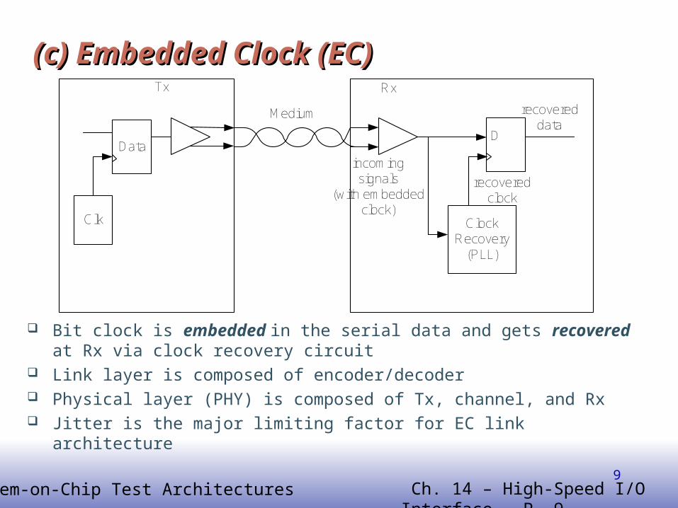
(c) Embedded Clock (EC) (c) Embedded Clock (EC)
Bit clock is embedded in the serial data and gets recovered at Rx via clock recovery circuit
Link layer is composed of encoder/decoder Physical layer (PHY) is composed of Tx, channel, and Rx Jitter is the major limiting factor for EC link architecture
incoming signals
(with embedded clock)
Clock Recovery
(PLL)
recovered clock
recovered data
Clk
Data
Tx Rx
Medium
D
EE141System-on-Chip Test Architectures Ch. 14 – High-Speed I/O Interface - P. 1010
Basics on Jitter, Noise, and Bit Error Rate (BER)Basics on Jitter, Noise, and Bit Error Rate (BER)
EE141System-on-Chip Test Architectures Ch. 14 – High-Speed I/O Interface - P. 1111
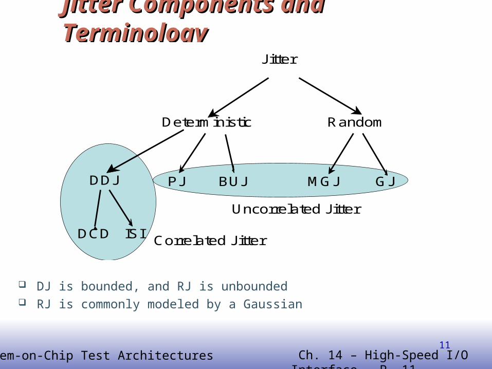
Jitter Components and TerminologyJitter Components and Terminology
Jitter
Random
DDJ PJ MGJ GJBUJ
Deterministic
DCD ISI Correlated Jitter
Uncorrelated Jitter
DJ is bounded, and RJ is unbounded RJ is commonly modeled by a Gaussian
EE141System-on-Chip Test Architectures Ch. 14 – High-Speed I/O Interface - P. 1212
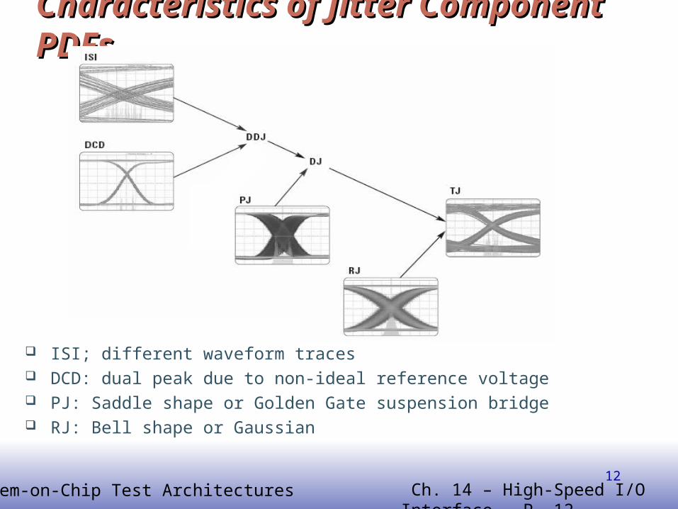
Characteristics of Jitter Component PDFsCharacteristics of Jitter Component PDFs
ISI; different waveform traces DCD: dual peak due to non-ideal reference voltage PJ: Saddle shape or Golden Gate suspension bridge RJ: Bell shape or Gaussian
EE141System-on-Chip Test Architectures Ch. 14 – High-Speed I/O Interface - P. 1313
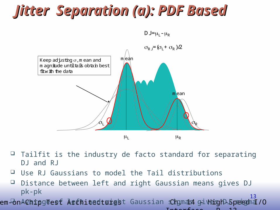
Jitter Separation (a): PDF BasedJitter Separation (a): PDF Based
Tailfit is the industry de facto standard for separating DJ and RJ Use RJ Gaussians to model the Tail distributions Distance between left and right Gaussian means gives DJ pk-pk Average of left and right Gaussian sigmas gives DJ sigma
Keep adjusting , mean and magnitude until tails obtain best fit with the data
L R
L R
DJ=L- R
RJ=(L+ R)/2
mean
mean
EE141System-on-Chip Test Architectures Ch. 14 – High-Speed I/O Interface - P. 1414
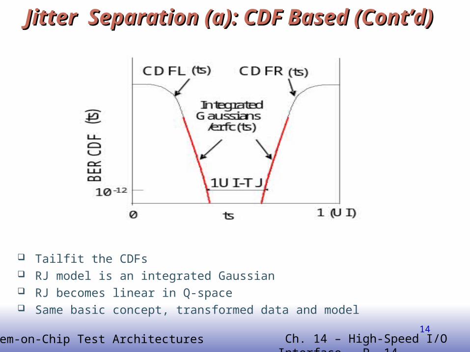
Jitter Separation (a): CDF Based (Cont’d)Jitter Separation (a): CDF Based (Cont’d)
Tailfit the CDFs RJ model is an integrated Gaussian RJ becomes linear in Q-space Same basic concept, transformed data and model
EE141System-on-Chip Test Architectures Ch. 14 – High-Speed I/O Interface - P. 1515
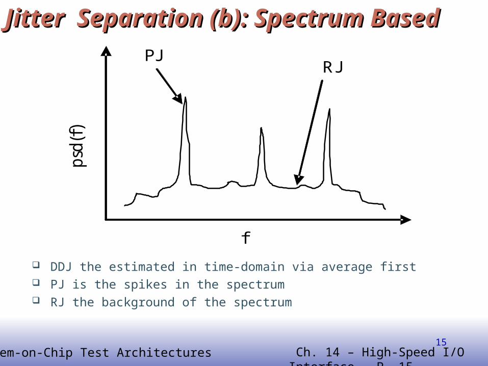
Jitter Separation (b): Spectrum BasedJitter Separation (b): Spectrum Based
DDJ the estimated in time-domain via average first PJ is the spikes in the spectrum RJ the background of the spectrum
f
psd
(f)
PJ RJ
EE141System-on-Chip Test Architectures Ch. 14 – High-Speed I/O Interface - P. 1616
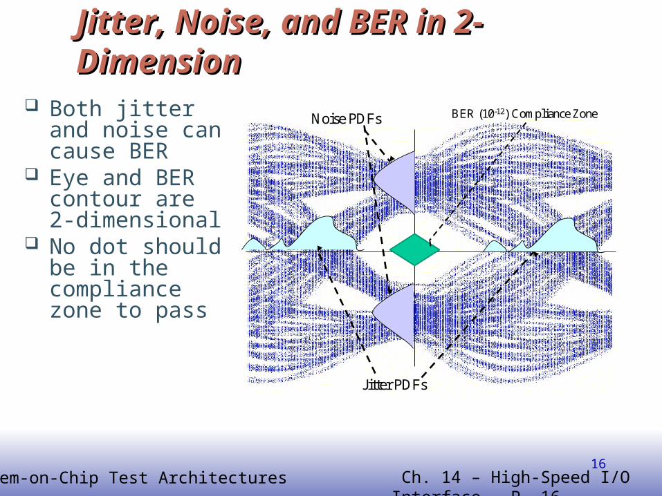
Jitter, Noise, and BER in 2-DimensionJitter, Noise, and BER in 2-Dimension
Noise PDFs
Jitter PDFs
BER (10-12) Compliance Zone Both jitter and
noise can cause BER
Eye and BER contour are 2-dimensional
No dot should be in the compliance zone to pass
EE141System-on-Chip Test Architectures Ch. 14 – High-Speed I/O Interface - P. 1717
II. Testing of I/O InterfacesII. Testing of I/O Interfaces
EE141System-on-Chip Test Architectures Ch. 14 – High-Speed I/O Interface - P. 1818
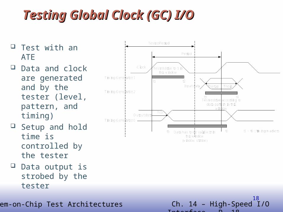
Testing Global Clock (GC) I/OTesting Global Clock (GC) I/O
Test with an ATE Data and clock are
generated and by the tester (level, pattern, and timing)
Setup and hold time is controlled by the tester
Data output is strobed by the tester
EE141System-on-Chip Test Architectures Ch. 14 – High-Speed I/O Interface - P. 1919
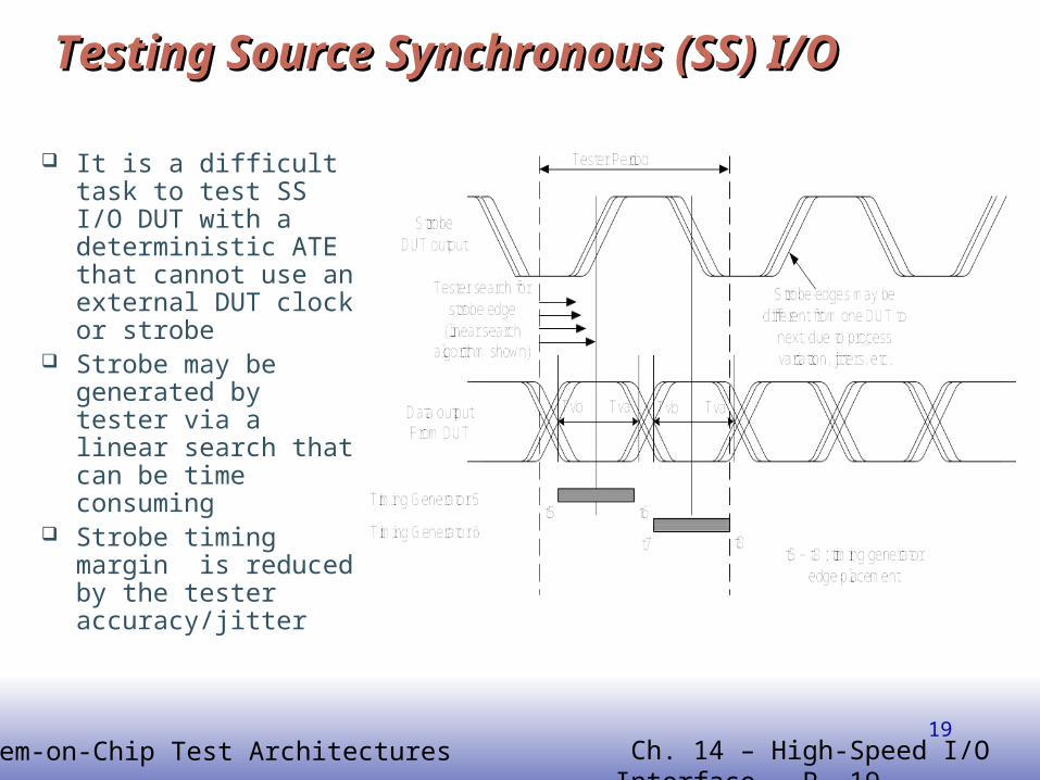
Testing Source Synchronous (SS) I/OTesting Source Synchronous (SS) I/O
It is a difficult task to test SS I/O DUT with a deterministic ATE that cannot use an external DUT clock or strobe
Strobe may be generated by tester via a linear search that can be time consuming
Strobe timing margin is reduced by the tester accuracy/jitter
EE141System-on-Chip Test Architectures Ch. 14 – High-Speed I/O Interface - P. 2020
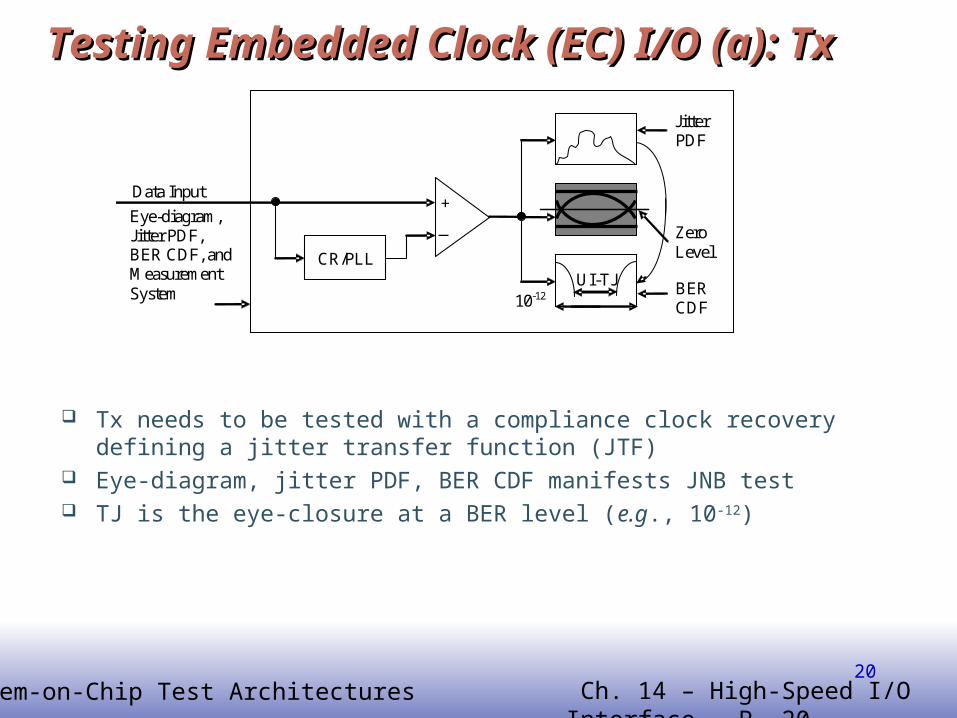
Testing Embedded Clock (EC) I/O (a): Tx Testing Embedded Clock (EC) I/O (a): Tx
Tx needs to be tested with a compliance clock recovery defining a jitter transfer function (JTF)
Eye-diagram, jitter PDF, BER CDF manifests JNB test TJ is the eye-closure at a BER level (e.g., 10-12)
+
_
CR/PLL UI-TJ BER
CDF
Zero Level
Jitter PDF
10-12
Data Input
Eye-diagram, Jitter PDF, BER CDF, and Measurement System
EE141System-on-Chip Test Architectures Ch. 14 – High-Speed I/O Interface - P. 2121
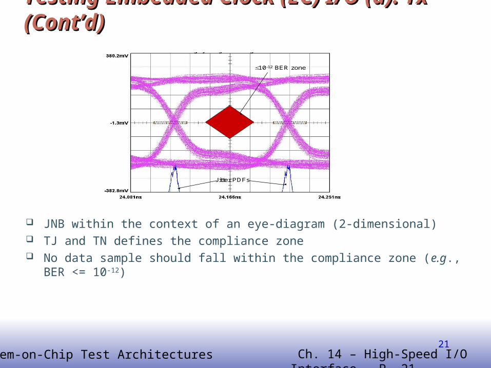
Testing Embedded Clock (EC) I/O (a): Tx (Cont’d) Testing Embedded Clock (EC) I/O (a): Tx (Cont’d)
10-12 BER zone
Jitter PDFs
JNB within the context of an eye-diagram (2-dimensional) TJ and TN defines the compliance zone No data sample should fall within the compliance zone (e.g., BER <= 10-12)
EE141System-on-Chip Test Architectures Ch. 14 – High-Speed I/O Interface - P. 2222
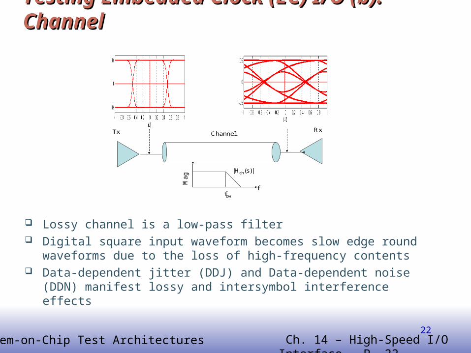
Testing Embedded Clock (EC) I/O (b): Channel Testing Embedded Clock (EC) I/O (b): Channel
Lossy channel is a low-pass filter Digital square input waveform becomes slow edge round waveforms due to
the loss of high-frequency contents Data-dependent jitter (DDJ) and Data-dependent noise (DDN) manifest lossy
and intersymbol interference effects
Tx RxChannel
fM
ag
fbw
|Hch(s)|
EE141System-on-Chip Test Architectures Ch. 14 – High-Speed I/O Interface - P. 2323
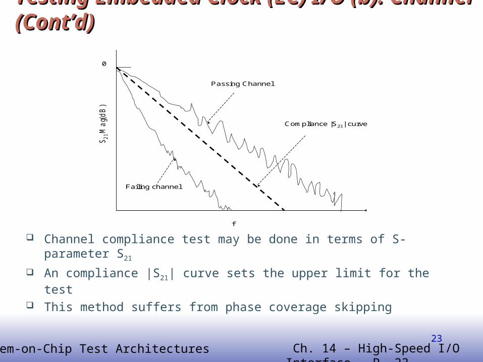
Testing Embedded Clock (EC) I/O (b): Channel (Cont’d) Testing Embedded Clock (EC) I/O (b): Channel (Cont’d)
Channel compliance test may be done in terms of S-parameter S21
An compliance |S21| curve sets the upper limit for the test This method suffers from phase coverage skipping
Compliance |S21| curve
Passing Channel
Failing channel
f
S2
1M
ag(
dB
)
0
EE141System-on-Chip Test Architectures Ch. 14 – High-Speed I/O Interface - P. 2424
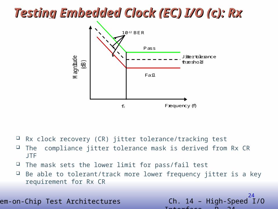
Testing Embedded Clock (EC) I/O (c): Rx Testing Embedded Clock (EC) I/O (c): Rx
Rx clock recovery (CR) jitter tolerance/tracking test The compliance jitter tolerance mask is derived from Rx CR JTF The mask sets the lower limit for pass/fail test Be able to tolerant/track more lower frequency jitter is a key requirement for
Rx CR
Frequency (f)f c
Jitter tolerance threshold
Pass
Fail
10-12 BER
EE141System-on-Chip Test Architectures Ch. 14 – High-Speed I/O Interface - P. 2525
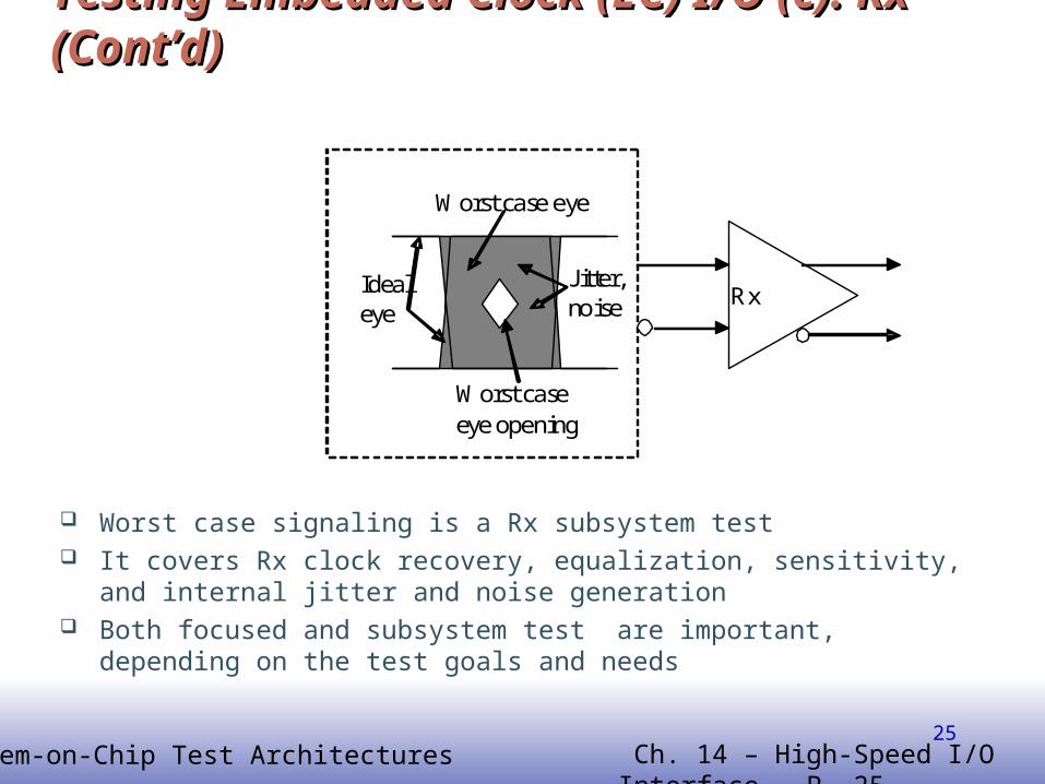
Testing Embedded Clock (EC) I/O (c): Rx (Cont’d) Testing Embedded Clock (EC) I/O (c): Rx (Cont’d)
Worst case signaling is a Rx subsystem test It covers Rx clock recovery, equalization, sensitivity, and internal jitter and
noise generation Both focused and subsystem test are important, depending on the test goals
and needs
Rx
Worst case eye
Worst case eye opening
Ideal eye
Jitter, noise
EE141System-on-Chip Test Architectures Ch. 14 – High-Speed I/O Interface - P. 2626
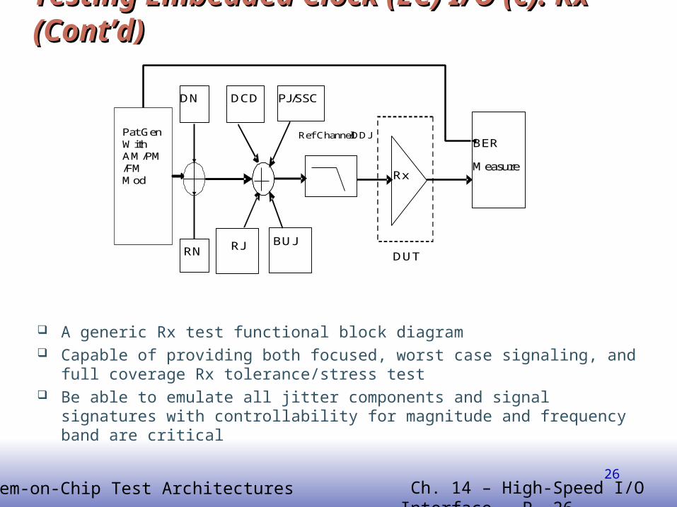
Testing Embedded Clock (EC) I/O (c): Rx (Cont’d) Testing Embedded Clock (EC) I/O (c): Rx (Cont’d)
A generic Rx test functional block diagram Capable of providing both focused, worst case signaling, and full coverage
Rx tolerance/stress test Be able to emulate all jitter components and signal signatures with
controllability for magnitude and frequency band are critical
Rx
DCD
RJ
BER
Measure
BUJ
PJ/SSC
Ref Channel/DDJ
DUT
Pat Gen With AM/PM/FM Mod
DN
RN
EE141System-on-Chip Test Architectures Ch. 14 – High-Speed I/O Interface - P. 2727
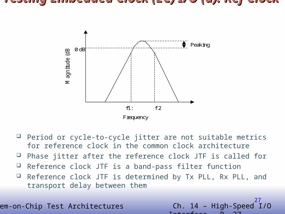
Testing Embedded Clock (EC) I/O (d): Ref Clock Testing Embedded Clock (EC) I/O (d): Ref Clock
Period or cycle-to-cycle jitter are not suitable metrics for reference clock in the common clock architecture
Phase jitter after the reference clock JTF is called for Reference clock JTF is a band-pass filter function Reference clock JTF is determined by Tx PLL, Rx PLL, and transport delay
between them
0 dB
f1: f 2
Frequency
Mag
nit
ude
(dB
)
Peaking
EE141System-on-Chip Test Architectures Ch. 14 – High-Speed I/O Interface - P. 2828
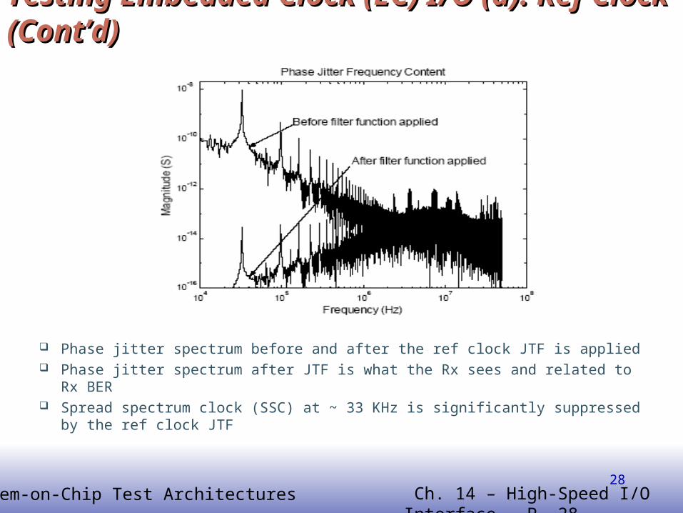
Testing Embedded Clock (EC) I/O (d): Ref Clock (Cont’d) Testing Embedded Clock (EC) I/O (d): Ref Clock (Cont’d)
Phase jitter spectrum before and after the ref clock JTF is applied Phase jitter spectrum after JTF is what the Rx sees and related to Rx BER Spread spectrum clock (SSC) at ~ 33 KHz is significantly suppressed by the
ref clock JTF
EE141System-on-Chip Test Architectures Ch. 14 – High-Speed I/O Interface - P. 2929
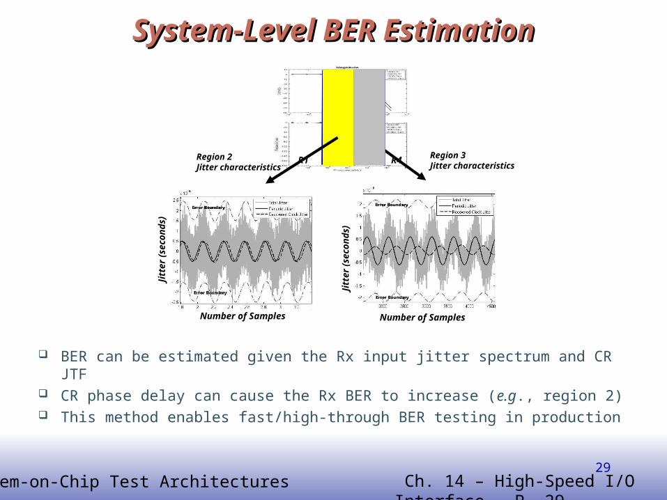
System-Level BER EstimationSystem-Level BER Estimation
BER can be estimated given the Rx input jitter spectrum and CR JTF CR phase delay can cause the Rx BER to increase (e.g., region 2) This method enables fast/high-through BER testing in production
R1 R2 R3 R4
Number of Samples
Jitt
er (
seco
nd
s)
Jitt
er (
seco
nd
s)
Number of Samples
Region 2 Jitter characteristics
Region 3 Jitter characteristics
EE141System-on-Chip Test Architectures Ch. 14 – High-Speed I/O Interface - P. 3030
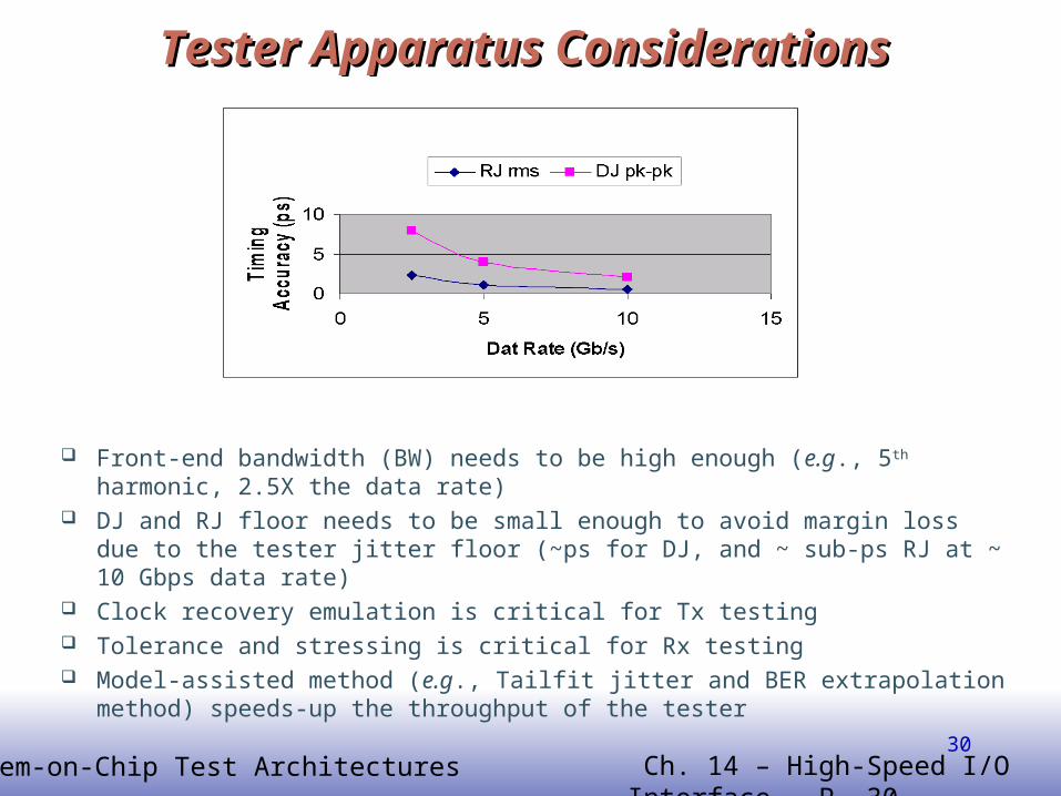
Tester Apparatus Considerations Tester Apparatus Considerations
Front-end bandwidth (BW) needs to be high enough (e.g., 5th harmonic, 2.5X the data rate)
DJ and RJ floor needs to be small enough to avoid margin loss due to the tester jitter floor (~ps for DJ, and ~ sub-ps RJ at ~ 10 Gbps data rate)
Clock recovery emulation is critical for Tx testing Tolerance and stressing is critical for Rx testing Model-assisted method (e.g., Tailfit jitter and BER extrapolation method)
speeds-up the throughput of the tester
Tetser Accuracy Requirements
0
5
10
0 5 10 15
Dat Rate (Gb/s)
Tim
ing
Ac
cu
rac
y (
ps
)
RJ rms DJ pk-pk
EE141System-on-Chip Test Architectures Ch. 14 – High-Speed I/O Interface - P. 3131
III. DFT-Assisted TestIII. DFT-Assisted Test
EE141System-on-Chip Test Architectures Ch. 14 – High-Speed I/O Interface - P. 3232
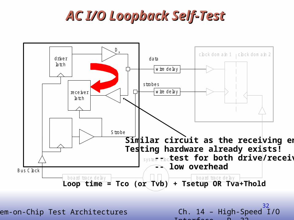
AC I/O Loopback Self-Test AC I/O Loopback Self-Test
driverla tch
D x
S trobe
B us C lock
board trace de lay
w ire de lay
w ire de lay
board trace de lay
system clock
clock dom ain 1 clock dom ain 2data
strobes
rece iverla tch
Similar circuit as the receiving end!Testing hardware already exists!
-- test for both drive/receive-- low overhead
Loop time = Tco (or Tvb) + Tsetup OR Tva+Thold
EE141System-on-Chip Test Architectures Ch. 14 – High-Speed I/O Interface - P. 3333
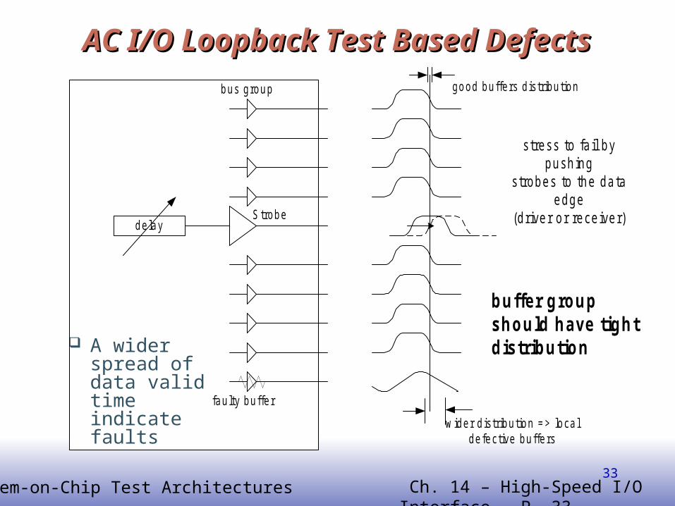
S trobede lay
stress to fa il bypushing
strobes to the dataedge
(driver or receiver)
buffer groupshould have tightdistribution
bus group
fau lty buffe r
good buffe rs d istribu tion
w ider d istribu tion => loca lde fective bu ffe rs
AC I/O Loopback Test Based DefectsAC I/O Loopback Test Based Defects
A wider spread of data valid time indicate faults
EE141System-on-Chip Test Architectures Ch. 14 – High-Speed I/O Interface - P. 3434
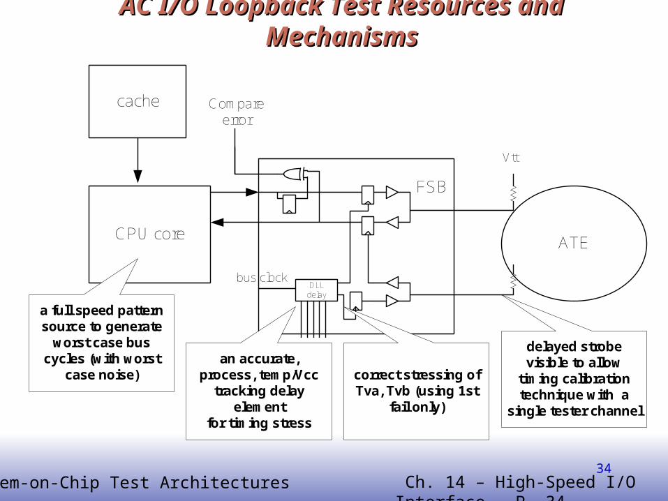
AC I/O Loopback Test Resources and MechanismsAC I/O Loopback Test Resources and Mechanisms
cache
CPU coreATE
Compare error
Vtt
FSB
a full speed pattern source to generate
worst case bus cycles (with worst
case noise)
delayed strobe visible to allow
timing calibration technique with a
single tester channel
DLL delay
an accurate, process, temp/Vcc
tracking delay element
for timing stress
bus clock
correct stressing of Tva, Tvb (using 1st
fail only)
EE141System-on-Chip Test Architectures Ch. 14 – High-Speed I/O Interface - P. 3535
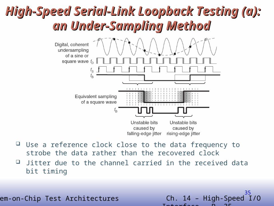
High-Speed Serial-Link Loopback Testing (a): an High-Speed Serial-Link Loopback Testing (a): an Under-Sampling Method Under-Sampling Method
Use a reference clock close to the data frequency to strobe the data rather than the recovered clock
Jitter due to the channel carried in the received data bit timing
EE141System-on-Chip Test Architectures Ch. 14 – High-Speed I/O Interface - P. 3636
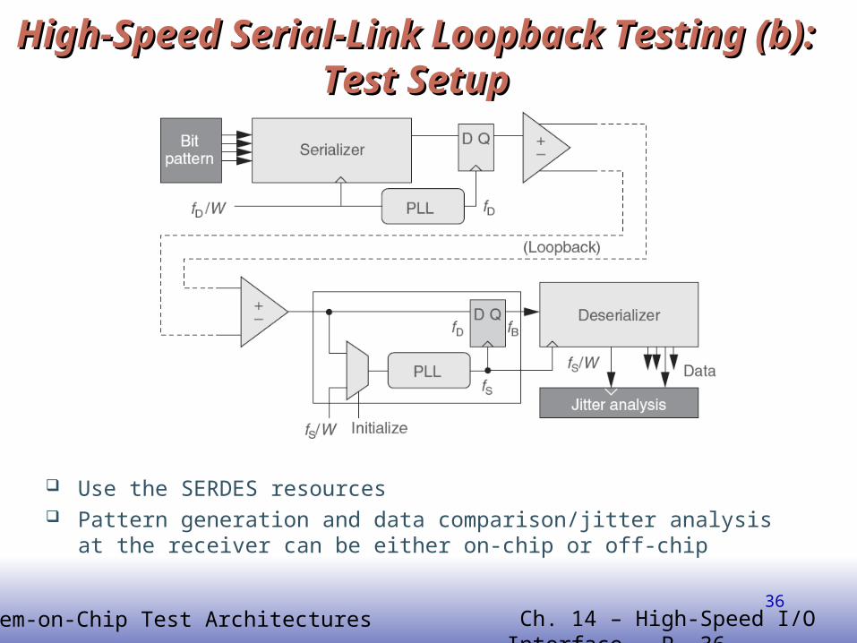
High-Speed Serial-Link Loopback Testing (b): Test High-Speed Serial-Link Loopback Testing (b): Test SetupSetup
Use the SERDES resources Pattern generation and data comparison/jitter analysis at the receiver can be
either on-chip or off-chip
EE141System-on-Chip Test Architectures Ch. 14 – High-Speed I/O Interface - P. 3737
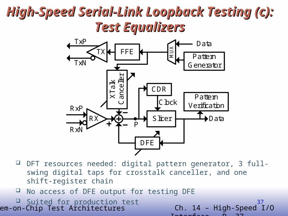
High-Speed Serial-Link Loopback Testing (c): Test High-Speed Serial-Link Loopback Testing (c): Test EqualizersEqualizers
DFT resources needed: digital pattern generator, 3 full-swing digital taps for crosstalk canceller, and one shift-register chain
No access of DFE output for testing DFE Suited for production test
Slicer
DFE
CDR
XT
alk
Can
celle
r
FFE
Data
DataTX
RX
PatternGenerator
MU
X
RxP
RxN
ClockPattern
Verification
TxN
TxP
P
EE141System-on-Chip Test Architectures Ch. 14 – High-Speed I/O Interface - P. 3838
IV. System-Level Interconnect TestingIV. System-Level Interconnect Testing
EE141System-on-Chip Test Architectures Ch. 14 – High-Speed I/O Interface - P. 3939
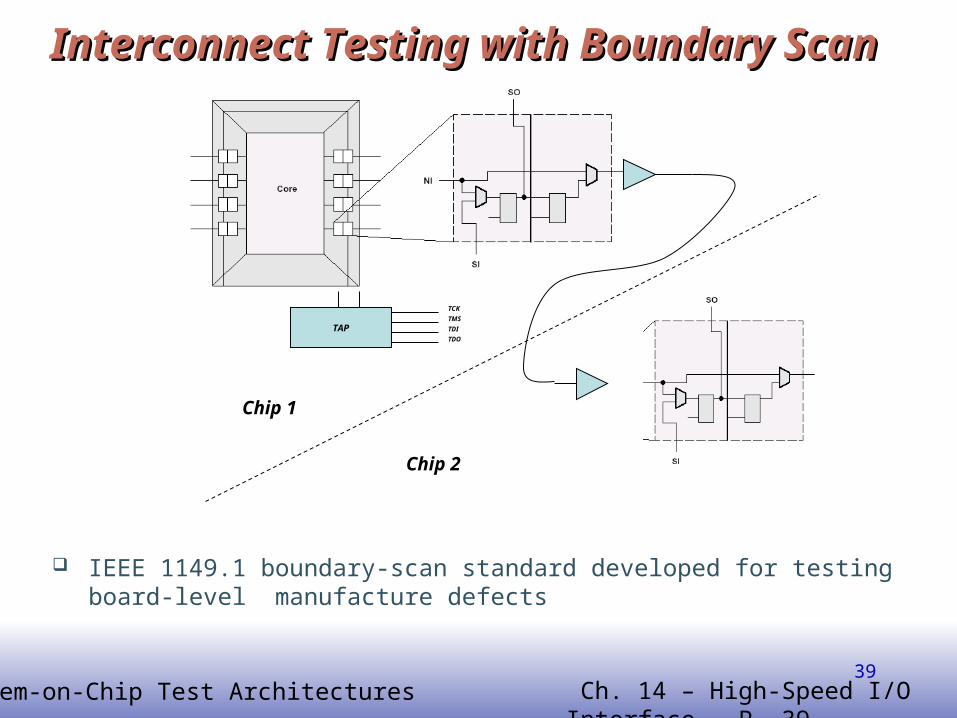
Interconnect Testing with Boundary ScanInterconnect Testing with Boundary Scan
IEEE 1149.1 boundary-scan standard developed for testing board-level manufacture defects
Chip 1
TAP
TCK
TMS
TDI
TDO
Chip 2
EE141System-on-Chip Test Architectures Ch. 14 – High-Speed I/O Interface - P. 4040
Interconnect Testing with High-Speed Boundary ScanInterconnect Testing with High-Speed Boundary Scan
IEEE 1149.1 boundary-scan standard has been extended to IEEE 1149.6 for high-speed boundary-scan test.
IEEE 1149.6 supports AC-coupled differential signaling. Digital driver logic and digital receiver logic along with the
analog test receiver are added to support the high-speed differential signaling, under the control of the 1149.1 TAP controller.
More information about 1149.6 can be found in Chapter 1. However, its reliability for testing Gbps I/O interfaces
remains to be a problem for IEEE 1149.6.
EE141System-on-Chip Test Architectures Ch. 14 – High-Speed I/O Interface - P. 4141
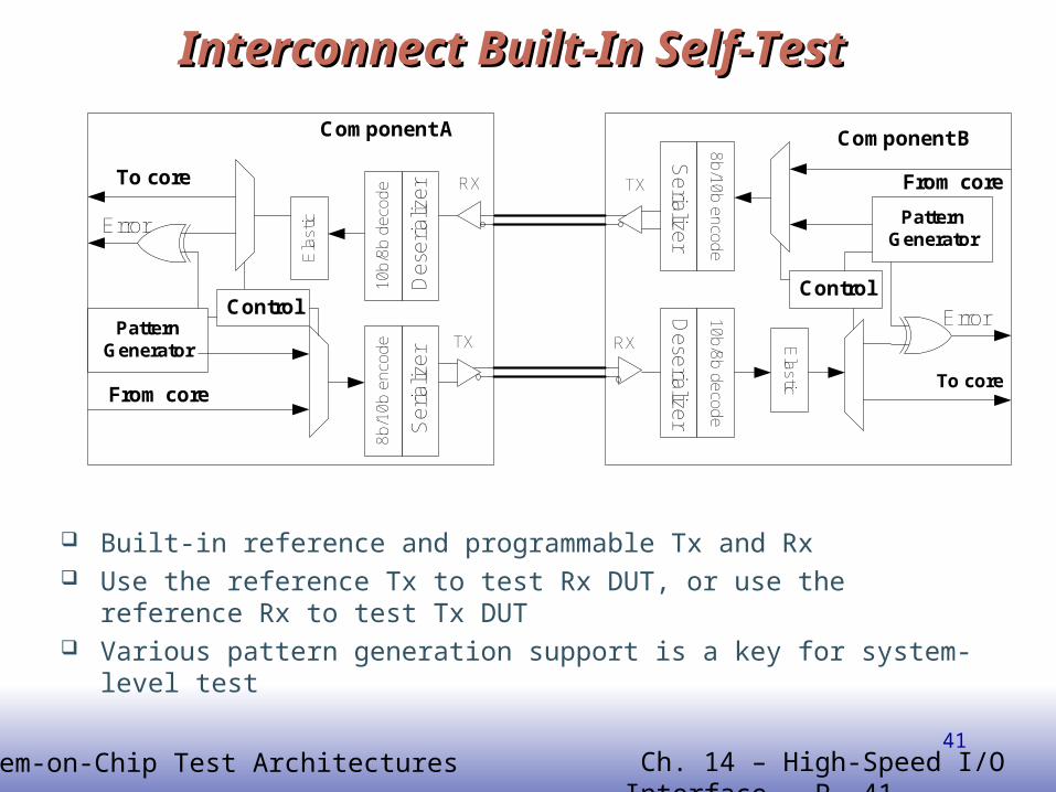
Interconnect Built-In Self-TestInterconnect Built-In Self-Test
Built-in reference and programmable Tx and Rx Use the reference Tx to test Rx DUT, or use the reference Rx to test Tx DUT Various pattern generation support is a key for system-level test
To core
Component B
TX
Deserializer
Elastic
RX
From core
Pattern Generator
Error
Control
10b/8b decode8b/10b encode
Serializer
To core
Component A
TX
Des
eria
lizer
Ela
stic
RX
From core
Pattern Generator
Error
10b/
8b d
ecod
e8b
/10b
enc
ode
Ser
ializ
er
Control
EE141System-on-Chip Test Architectures Ch. 14 – High-Speed I/O Interface - P. 4242
V. Future Challenges V. Future Challenges
EE141System-on-Chip Test Architectures Ch. 14 – High-Speed I/O Interface - P. 4343
Future ChallengesFuture Challenges Data rate keeps increasing Link jitter margin gets smaller, device components and tester have to be
more accurate Eye-will be closed at the Rx input, reference Tx and Rx will be mandatory for
testing Advanced signaling/equalizations (Tx, Rx, continuous, discrete, linear,
adaptive) More complex link system, Tx and Rx subsystems means more complex test
requirements Femto second (fs) accuracy is coming for 10 Gbps and higher Test solution should be optimized for accuracy, throughput, parallelism, fault
coverage, and cost requirements (somewhat conflicting), for both on-chip DFT/BIST and off-chip ATE/instruments
More analog DFT/BIST, adaptive design and test with low power Insuring JNB test quality from design characterization to high-volume
production with high-confidence and low cost
EE141System-on-Chip Test Architectures Ch. 14 – High-Speed I/O Interface - P. 4444
Concluding RemarksConcluding Remarks Three leading I/O architectures:
Global clock (GC), source synchronous (SS), and embedded Link architecture determines the relevant test parameters and
methods. Key parameters include: Data valid to clock/strobe, setup/hold times for GC and SS; jitter, noise, and BER (JNB) for embedded Clock recovery and equalization must be included in test DFE-assisted test methods:
Largely rely on loopback: AC loopback, under-sampling loopback, and equalizer testing System-level test methods:
Boundary scan for testing manufacturing defects BIST for testing Tx and Rx, and link system
Future challenges: Higher data rate, smaller jitter margin, higher channel counter, better accuracy More complex test requirements and platform, more DFT/BIST to address cost and avoid tester-DUT interface bandwidth bottleneck