ee3121 computer system engineering academic year 2011/2012 beng subject code – ee3121 lecturer –...
TRANSCRIPT

EE3121 Computer System Engineering
Academic Year 2011/2012
BENG
Subject Code – EE3121
Lecturer – Y.F. Fung
Office (Y.F. Fung) : CF605
email: [email protected]
Consultation: Friday afternoon

Lab. ScheduleCommence in week 5
A briefing will be provided before the session
Form your own group and with 2 students per group
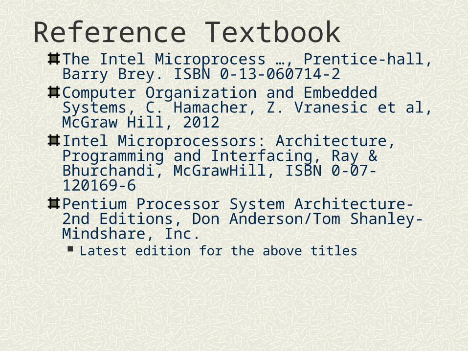
Reference TextbookThe Intel Microprocess …, Prentice-hall, Barry Brey. ISBN 0-13-060714-2Computer Organization and Embedded Systems, C. Hamacher, Z. Vranesic et al, McGraw Hill, 2012 Intel Microprocessors: Architecture, Programming and Interfacing, Ray & Bhurchandi, McGrawHill, ISBN 0-07-120169-6Pentium Processor System Architecture-2nd Editions, Don Anderson/Tom Shanley-Mindshare, Inc. Latest edition for the above titles

Reference books
IBM PC Assembly Language and Programming - Fourth Edition (Peter Abel - Prentice-Hall International Inc.)
The 8086 and 80286 Microprocessors Hardware, Software and Interfacing (A. Singh, W.A. Triebel, Prentice-Hall)

Teaching materials
Available in WebCT web site
Also some useful information can be found in ftp.ee.polyu.edu.hk/yffung/ee3231

Related TopicsComputer Architectures of microprocessors (2.5~3 weeks)Assembly Language programming (3 weeks)Memory system overview (2 weeks)Input/Output mechanism (2 weeks)Other computing supporting facilities: interrupt (1.5 weeks), communication (1.5 weeks)

Assessment methodsContinuous assessment (40%) Performance in Lab and online exercises (10%) Lab report (10%) Quiz (usually only 1 test or quiz) (usually
around week 8 or 9 after the first 3 topics) (20%)
Examine (60%)
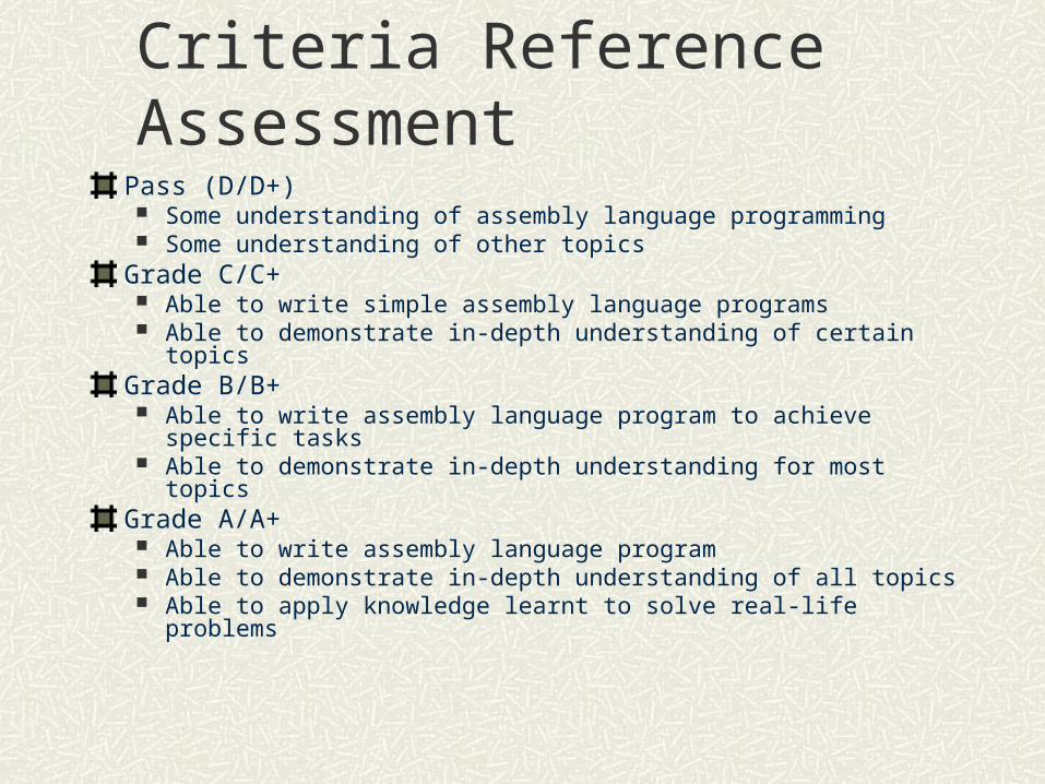
Criteria Reference AssessmentPass (D/D+) Some understanding of assembly language programming Some understanding of other topics
Grade C/C+ Able to write simple assembly language programs Able to demonstrate in-depth understanding of certain topics
Grade B/B+ Able to write assembly language program to achieve specific tasks Able to demonstrate in-depth understanding for most topics
Grade A/A+ Able to write assembly language program Able to demonstrate in-depth understanding of all topics Able to apply knowledge learnt to solve real-life problems

Objectives
To understand the basic principles (hardware components) of a computer system
To learn how to control a computer system using assembly language programming
To learn how to design a simple computer system (eg for the development of an electronic mouse, robot, simple control system for your project)

Learning outcomes1. Given specifications of an application and the
instruction set of the microprocessor, design an assembly program to carry out the necessary operations
2. able to appreciate advanced features of the latest microprocessors
3. given a set of conditions, design a simple computer system
4. able to think logically and be able to present results
Attention!!!!!!!!!!!!!
This is not a traditional “Engineering” subject!!!!!!!!
Equations – almost none!!!!!!
Try to think, understand and learn
Do not try to memorize

What is a computer ?????
Nowadays, computer comes in different forms!!!!!!!!!!!!!!!!!!!In this subject, we try to learn the generic form of a computer!!!!!!!!!!!!!!!!If you are willing to spend your time, it is possible to build your own game console or a cell phone

What is a computer?
Is the structure of a tablet very different from a traditional PC?

The PC is dead“It was fun while it lasted, but as of 2011 the era of the desktop computer is officially over.”
Read more: http://www.foxnews.com/scitech/2011/01/11/pc-is-dead-ces-tablets-smartphone/#ixzz1X1jBuY8N

Different forms of computerCan you think of a real-life example that involves the application of a microprocessor or a computer?

Computer is a digital system
Computer is a combination of digital and analogue systems, but mainly digital
So to learn this subject, you also need to understand basic digital system as well as binary number system

Number systems (revision)The microprocessor (µP) is a binary device, everything inside the microprocessor is represented by 0 and 1. The most direct number system used inside the microprocessor is the binary system (base 2) with only 0 and 1, for example 01010101. Each digit in the number represents a value in power of 2, starting from the RHS (Right hand side). The first digit is 20, then 21, 22 , etc. Usually, the most RHS bit is also called the LSB (least significant bit) while the most LHS bit is the MSB (most significant bit).So the value 01010101 = 0x27 + 1x26 + 0x25 + 1x24 + 0x23 + 1x22 + 0x21 + 1x20 = 64+16+4+1 = 85

Number system
In base 10 123 = 1x10² + 2x101 + 3x100
In subtraction 0-1 = 11 because there is no (-) sign in binary system. The first “1” is called the borrow bit
In addition 1+1 = 10 the first “1” is called the carry bit

Number systemIn addition, we use the term byte to represent an 8-bit data and the term word to represent 16-bit value, for a 32-bit value, it is called double word.If we want to represent a very large number then we need to use many bits and this is not very convenient. Therefore we usually use number systems derived from the binary system and the most commonly used number system are Octal (base 8) and hexademical (base 16) usually we just use the term Hex.

Hex number systemIn octal, only digits from 0 to 7 will be used and in hexadecimal, we use 0 to 9 and A, B, C, D, E, F to represent the values. A = 10, B = 11, C = 12, D = 13, E = 14, F = 15 To convert, from a binary number to a hex, it can be done very easily, starting from the RHS, every 4-bit from the binary number can be converted directly into a hex digit. For example: 0101 0101 is equal to 55H (H == hexadecimal), we have two 4-bit groups 0101 and 0101. The value 0101 = 5 so the binary pattern is 55H (in Hex).Example: 1100 0111 1010 1011 = C 7 A B H To convert back ABCDH = 1010 1011 1100 1101
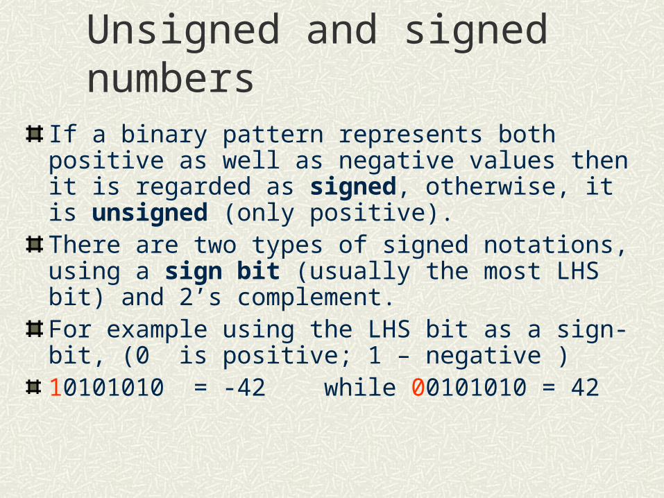
Unsigned and signed numbersIf a binary pattern represents both positive as well as negative values then it is regarded as signed, otherwise, it is unsigned (only positive).There are two types of signed notations, using a sign bit (usually the most LHS bit) and 2’s complement. For example using the LHS bit as a sign-bit, (0 is positive; 1 – negative )10101010 = -42 while 00101010 = 42
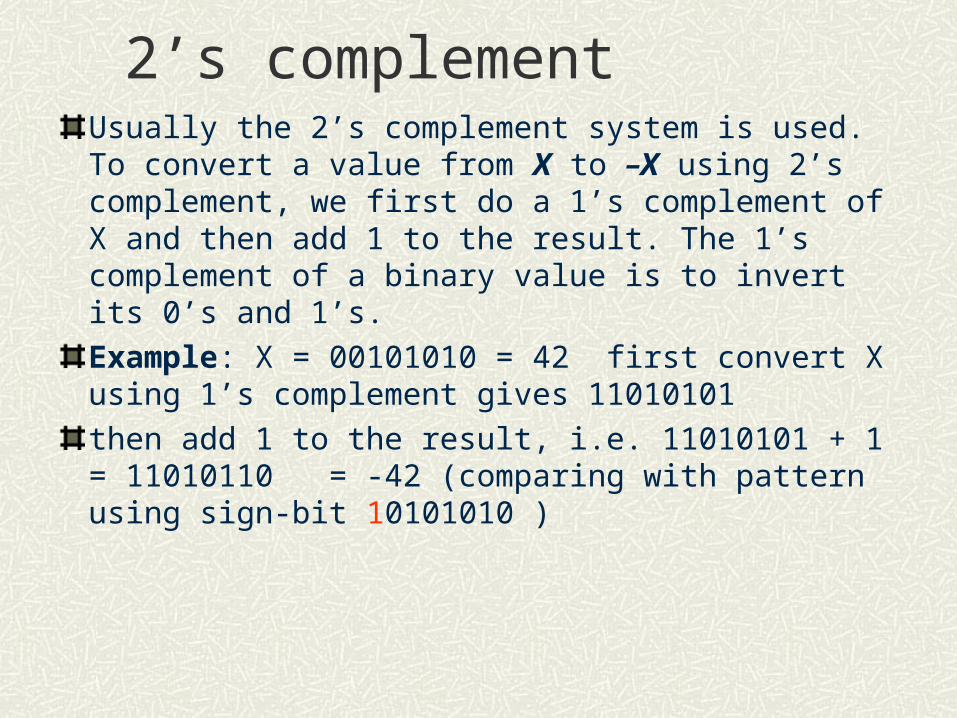
2’s complementUsually the 2’s complement system is used. To convert a value from X to –X using 2’s complement, we first do a 1’s complement of X and then add 1 to the result. The 1’s complement of a binary value is to invert its 0’s and 1’s.
Example: X = 00101010 = 42 first convert X using 1’s complement gives 11010101
then add 1 to the result, i.e. 11010101 + 1 = 11010110 = -42 (comparing with pattern using sign-bit 10101010 )

Floating point representationAs mentioned above, each digit in a binary pattern represents a value in the power of 2. In a floating point format, the digits after the decimal point represent value 2-1, 2-2, etc.
Example, 0.1010 = 1x2-1+0x2-2+1x2-3+0x2-4 = 0.5+0.125 = 0.625How to represent signed floating point values?

Floating-point format
Floating-point numbers are represented in the form X = ±F •2 ±E
F is called the fraction (or mantissa) and E is the exponentFloating-point number is usually represented in two standard (defined by IEEE )32-bit (single precision) and 64-bit (double precision). A 80-bit (extended precision) standard is also available.
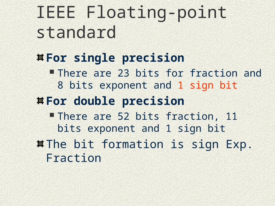
IEEE Floating-point standard
For single precision There are 23 bits for fraction and 8 bits
exponent and 1 sign bit
For double precision There are 52 bits fraction, 11 bits exponent and
1 sign bit
The bit formation is sign Exp. Fraction

Floating-point arithmetic
Using the format ±F •2 ±E can implement floating point arithmetic very easily
X = a x 2 b
Y = c x 2 d
X*Y = (axc)* 2 (b+d)
X/Y = (a/c )* 2 (b-d)
How about X+Y and X-Y ??????
Floating-point format
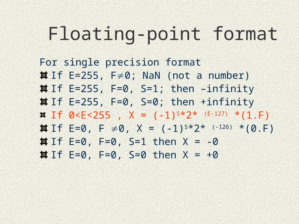
For single precision formatIf E=255, F0; NaN (not a number)If E=255, F=0, S=1; then –infinityIf E=255, F=0, S=0; then +infinityIf 0<E<255 , X = (-1)S*2* (E-127) *(1.F)If E=0, F 0, X = (-1)S*2* (-126) *(0.F)If E=0, F=0, S=1 then X = -0If E=0, F=0, S=0 then X = +0

Example of floating point Given 6.125 express the value in binary format using single precision floating-point format First convert the value into the format 1.XXX*2y
6.125 = 1.53125 x 22
So the exponent is 2 and the fraction is 1.53125 As all floating-point values always come with the ‘1.’
so the ‘1.’ is not stored and only 53125 is saved!!!! 0.53125 = .10001 0 10000001 10001000000000000…
E-127 = 2 => E=129

ExerciseConvert the number -4.5 into a IEEE 32-bit floating-point pattern
Convert 9 into a IEEE 32-bit floating point
Without using a calculator, determine 01010010 + 10101101
Without using a calculator, determine 01010010 – 10101101
Characters
In addition to values, characters are also represented using binary codes usually in ASCII (American Standard Code for Information Interchange) code.

ASCII table
A = 41H ; a = 61H so a>A

Chinese characters
Chinese characters and other non-ASCII characters are represented by two bytes
There are different coding systems to represent Chinese characters such as Unicode, Big5 etc.
A font file must be installed in order to display the corresponding characters

Big 5 codeEvery Chinese Character is represented by a two byte code. The first byte ranges from 0xA1 to 0xF9, while the second byte ranges from 0x40 to 0x7E, 0xA1 to 0xFE
Since the MSB of the two byte code is always set. Thus, in a document that contain Chinese characters and regular ASCII characters, the ASCII characters are still represented with a single byte.

Some examples
Address Character
A640H 共AF66H 病A741H 你 AA46H 東

Revision exercisesWhat is a Bit, a byte, a word, one K, one M What is Hex, Oct, binaryDo you know how to convert a number into different base systems without using a calculator?Binary number notation (10101010 = ???)How many different values can be represented by a 8-bit pattern?Hexadecimal A = ??? How to convert binary 1101010101110101 to Hex?CFH (Hex) = ???
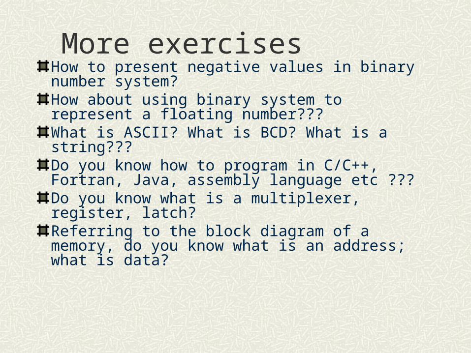
More exercisesHow to present negative values in binary number system?How about using binary system to represent a floating number???What is ASCII? What is BCD? What is a string???Do you know how to program in C/C++, Fortran, Java, assembly language etc ???Do you know what is a multiplexer, register, latch? Referring to the block diagram of a memory, do you know what is an address; what is data?
Microprocessor/Microcomputer
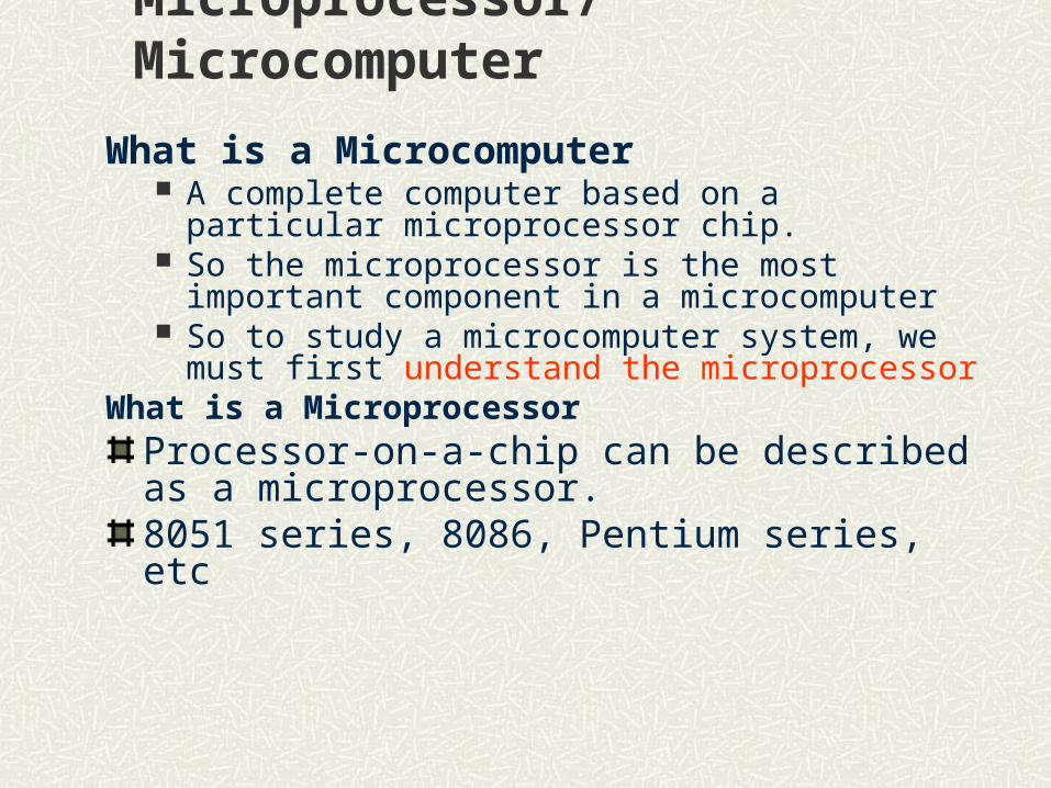
What is a Microcomputer A complete computer based on a particular
microprocessor chip. So the microprocessor is the most important component
in a microcomputer So to study a microcomputer system, we must first
understand the microprocessorWhat is a Microprocessor
Processor-on-a-chip can be described as a microprocessor.8051 series, 8086, Pentium series, etc

Block diagram of a generic microcomputer system
Data and address bus
RAM
Keyboard, mouseMonitor, printer
Hard DiskCD ROM

Microprocessor based system such as an electronic mouse
uP withControl program
sensor motor
InputOutput

Structure of a modern computer system

Model Year Max. Clock frequency at introduction
Transistors per Die
Register Sizes
Ext. data bus size
Max. external address space
Caches
8086 1978 8 MHz 29K 16GP 16 1MB None
486 1989 25MHz 1.2M 32GP80FPU
32 4GB L1:8KB
Pentium 1993 60MHz 3.1M 32GP80FPU
64 4GB L1:16KB
P3 1999 500MHz 8.2M 32GP80FPU64MMX128 XMM
64 64GB L1:32KBL2: 512KB
Pentium Dual Core
2007 1.6GHz to 2.4 GHz
167 M 64 64GB L2: 1MB
GP – general purposeFPU – floating point unit Register – a device to store binary data

Features of microprocessorOperating frequency
Size of register and how many?
Size of data bus
Size of address bus
Size of cahce
Number of core

Different types of microprocessorMicroprocessors can also be classified based on the instructions. There are two fundamentally different approaches in the design of instruction set. One popular approach is called Reduced Instruction Set Computers (RISC). In a RISC, each instruction occupies exactly one word. Examples include ARM, PIC.
Devices using ARM processor – Blackberry
Cortex processor is also from ARM

CISCAn alternative to RISC is to make use of more complex instructions which may span more than one word of memory, and which may specify more complicated operations. Processors based on this idea is called Complex Instruction Set Computer (CISC). The Intel x86 CPUs and AMD processors are examples of CISC

The Intel 8086 MicroprocessorThe 8086 is a popular device used in the early 70’s and 80’s and its architecture is simple and suitable for teaching computer architectureOnce we gain the basic concept of the 8086, we can then discuss the more advanced microprocessorsMany features found in 8086 are still being embedded in modern microprocessors but enhanced!
8086 Microprocessor
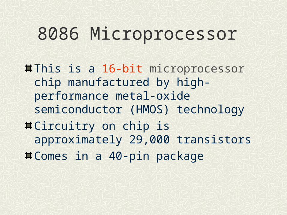
This is a 16-bit microprocessor chip manufactured by high-performance metal-oxide semiconductor (HMOS) technology
Circuitry on chip is approximately 29,000 transistors
Comes in a 40-pin package

Self test
Do you know what does it mean by 16-bit, 32-bit, or 64-bit processor?
How would you describe an Intel Core2 Duo CPU ?
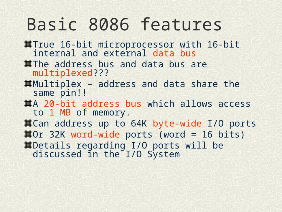
Basic 8086 featuresTrue 16-bit microprocessor with 16-bit internal and external data busThe address bus and data bus are multiplexed???Multiplex – address and data share the same pin!!A 20-bit address bus which allows access to 1 MB of memory. Can address up to 64K byte-wide I/O portsOr 32K word-wide ports (word = 16 bits) Details regarding I/O ports will be discussed in the I/O System
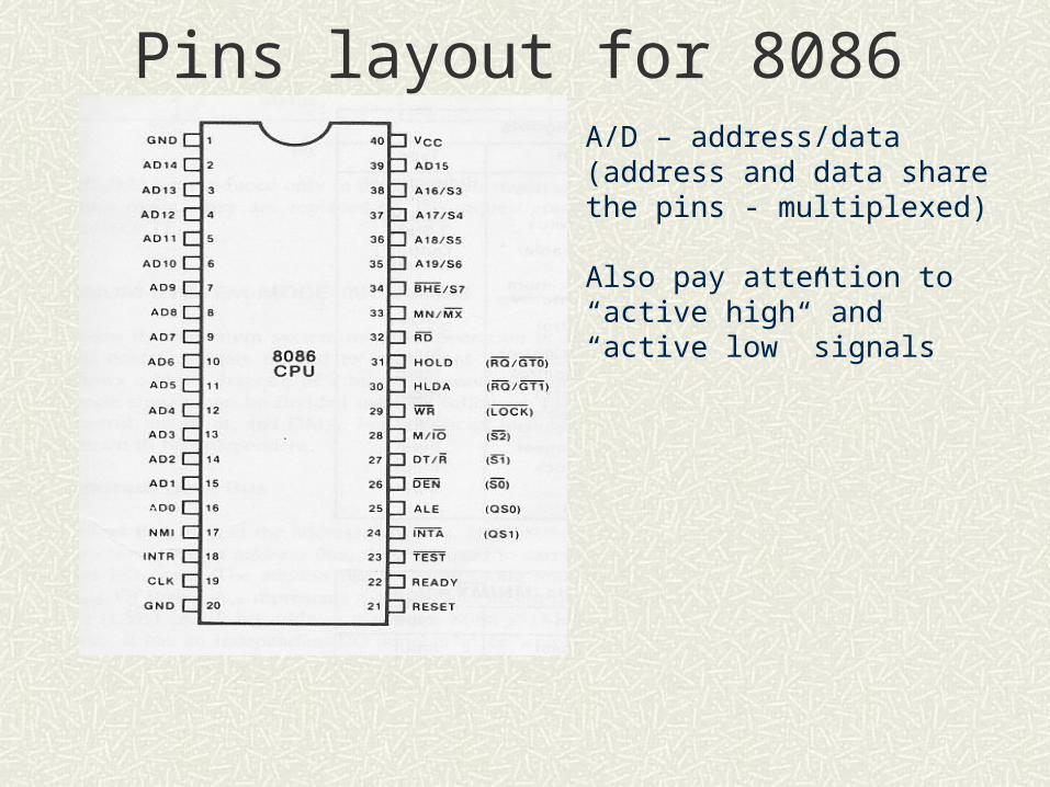
Pins layout for 8086A/D – address/data (address and data share the pins - multiplexed)
Also pay attention to “active high” and “active low” signals

8086 FeaturesThe 8086 has two modes – min. and max.
Min. mode – used as a typical microprocessor
Max. mode – use with multiple processors, usually for floating-point arithmetic)
The mode selection is via the MN/MX input

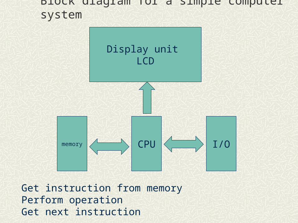
Block diagram for a simple computer system
CPUmemory
Display unit LCD
I/O
Get instruction from memory Perform/Execute operation Get next instruction
What are the basic operationsperformance by a computer?

What are the basic operations performed by a microprocessor?
Get instruction from memory
Perform/Execute operation
Get next instruction
So inside the microprocessor, it is organized into two units: Bus Interface Unit (BIU) and Execution Unit (EU). So that it can perform the above operations effectively

Processor Model for 8086

The 8086 Internal Architecture The internal functions of the 8086 µP are divided between two separate processing units. They are the Bus Interfacing Unit (BIU) and the Execution Unit (EU).
The BIU is responsible for performing all bus operations, such as instruction fetching, reading and writing operands from/to memory, and inputting and outputting of data for peripherals.
The EU is responsible for executing instructions
The two units operate asynchronously so overlapping instruction fetch and execution is possible (what’s the advantage of this???)

TerminologyProgram is stored in memory and consists of a sequence of instructions and some dataTo execute an instruction it may require some operandsWhat is an operand?Operand is the object that is being operated upon!Example, in an instruction ADD A, B (A = A+B)ADD (addition is the operation) A and B are the operands

Bus Interfacing Unit (BIU)The BIU is the 8086’s interface to the outside world (external memory). The major task of BIU is to get “information” from the memoryInformation includes data and instructionsHow can we get data from memory?????To access the memory, we need to issue an address (via the address bus) and then read the data (via the data bus) (Details of this mechanism will be discussed when we discuss the memory systems)
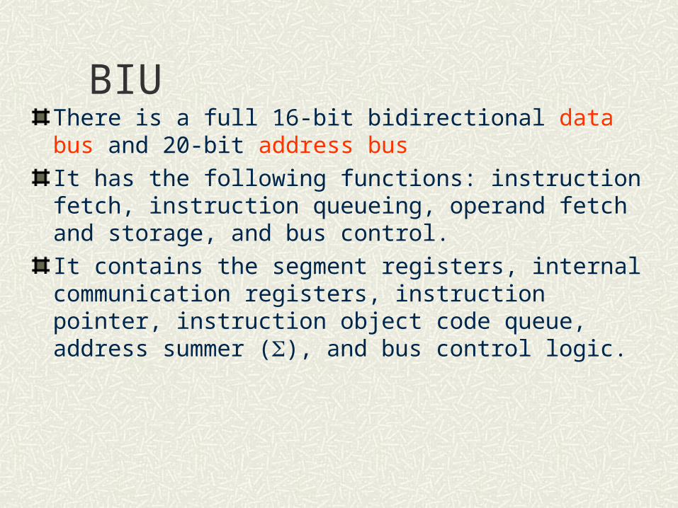
BIUThere is a full 16-bit bidirectional data bus and 20-bit address bus
It has the following functions: instruction fetch, instruction queueing, operand fetch and storage, and bus control.
It contains the segment registers, internal communication registers, instruction pointer, instruction object code queue, address summer (), and bus control logic.

How BIU and EU collaborateWhat a program consists of ???
A program is a collection of instructions and data
BIU fetch an instruction from memory and put it in the queue and this is called instruction queue (refer to the block diagram)
EU fetches the instruction from the queue and executes
BIU and EU implements a pipeline (BIU->EU) and pre-fetch to optimize the performance
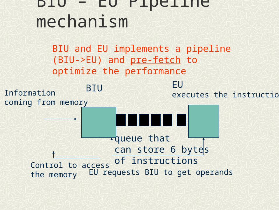
BIU – EU Pipeline mechanism
BIU EUexecutes the instruction
queue that can store 6 bytesof instructions
Informationcoming from memory
Control to access the memory EU requests BIU to get operands
BIU and EU implements a pipeline (BIU->EU) and pre-fetch to optimize the performance

Buffet - pre-fetch

Pre-fetch conceptPre-fetching is similar to what you do when you’re having a buffet dinner. You collect different kinds of food from the buffet table, for example, you take the sashimi, roast beef, soup, and salad etc. When you’re eating the salad, you have already pre-fetched the sashimi and the roast beef! If you do not pre-fetch then you take the salad first, go back to the table, eat your salad. When you finish the salad then you go and get some other food. Why pre-fetching your food??????

Pre-fetch by BIUWhat’s pre-fetch????When the queue can store at least 2 bytesEU is not requesting BIU to read or write operands from memoryBIU will look ahead in the program by prefetching the next sequential instructionThe prefetched instructions are held in the queue which is a FIFO (First-in-first-out) deviceTwo bytes are fetched (16-bit data bus) in a single memory cycleEU will read one instruction byte from the output of the queue

Pre-fetch
Int1a
Int1b
Int2a
Int2b
Int2c
Int3a
Int3b
Int4a
Memory
Queue
int1aint1bEU
int1bint2aint2b
int1a
While EU is processing “int1a”Int2a and int2b havealready been Pre-fetched

Instruction sequence
Fetch Execute Fetch Execute Fetch Execute
Time
Time

Pre-fetching by BIU
If the instruction queue is full (or there is only 1 empty slot) and EU is not requesting access to operands in memory, the BIU does not perform any bus cycles – this is called idle states
When BIU is in the process of fetching an instruction when the EU requests its services then BIU first completes the instruction fetch bus cycle and then serves the EU
ExerciseAn instruction can be completed by a single processing stage and it takes 25 clock cycles to finish. On the other hand, the instruction can be divided into five sub-tasks each of which can be carried out by one processing stage forming a pipeline. If sub-task 1 takes 10 clock cycles, sub-task 2 takes 5 clock cycles, sub-task 3 takes 8 clock cycles, sub-task 4 takes 10 clock cycles and sub-task 5 takes 12 clock cycles, how many instructions should be executed so that the sub-task approach will be more cost-effective?

Answer
Each sub-unit can only process one instruction at each time
45+(x-1)*12 <= 25*x So 2.53<= x If the number of instruction is 3 then the sub-task approach is faster

Pre-fetch
Is pre-fetching in a buffet dinner exactly the same as the pre-fetching mechanism in a microprocessor?
The plate is equivalent to which component?
Is a bigger plate is better than a small plate?

Components in the BIUBIU is to read/write the memory What is needed to access the memory???We need to generate an address and read/write the dataBIU contains a dedicated adder () which is used to generate the physical address of the memory locationAddress is formed by adding an appended 16-bit segment address and a 16-bit offset address

Inside BIUExample: the physical address of the next instruction to be fetched is formed by combining the current contents of the code segment (CS) register (16-bit) and the current contents of the instruction pointer (IP) register (16-bit)Register is a hardware device to store the binary data so 16-bit register is a device that can store a 16-bit data

Generating the physical addressIf CS (code segment) is 1005HThe IP is 5555HWhat is the physical address? (how to determine the physical address?)Point to consider: the address bus of the 8086 is 20-bit, the registers are 16-bit. Is it a problem????Consider the sum of two 16-bit values, what is the max. integer value represented by 16-bit. What is the sum and how many bits are required to represent the sum?

Segment concept8086 can support up to 1M memory
Memory is divided into segments
Each segment is 64K
To access data inside a segment, we need to know the base address of a segment as well as the offset.
This is similar to an address. You live it flat 11B so 11 is the base and B is the offset.

Segment in 8086
Why segment mechanism is needed in 8086? The address bus size (20-bit) > register size (16-bit)
Example: if the address bus is 4 bits then you can access 16 locations
If you can only output a 2-bit address from your register then what will happen?
Save components – can reduce the size of the registers
A segment is a 64Kbyte memory block
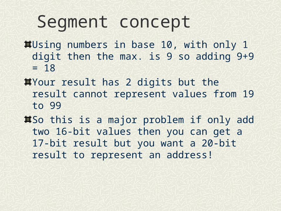
Segment conceptUsing numbers in base 10, with only 1 digit then the max. is 9 so adding 9+9 = 18
Your result has 2 digits but the result cannot represent values from 19 to 99
So this is a major problem if only add two 16-bit values then you can get a 17-bit result but you want a 20-bit result to represent an address!

Segment conceptSegment analogyIt is similar to a hotelIf you stay in hotel room number 1234 what does it imply? does it mean that the hotel has 1234 rooms?

Segment concept
1M
A 64k segment
A 64k segment
How can we access locationswithin a segment ??????

Segment Registers
The segment registers are used for accessing the memoryThe 8086 address space is segmented into 64K-byte segments and just four segments can be active at a time. Because there are only 4 segment registersIn theory, how many segments can we have???? Total memory 1M and segment is 64K so 1M/64K number of
segment

The Segment concept
Memory(a segment)
Base address (segment address)
Real address
Offset
So the real address (physical address) is =Base address (20 bits) + offset (16-bit)
The Base address must be divisible by 16 so the last digitis equal to 0 and the ‘0’ is notstored so a 16-bit register can hold the rest of the address
If base is 12340H and offset is 99H then the real address 123D9H

Segment concept
For example: FFFFEH is not divisible by 16 FFFF0H is divisible by 16 12340H is also divisible by 16

Segment concept
The maximum value of a 16-bit value is FFFF (Hex), if two 16-bit values added together, such as FFFF (segment) + FFFF (offset), the result is 1FFFE (Hex) (physical) and it is only a 17-bit value and values from 20000H to FFFFFH cannot be produced.
So in 8086, you cannot randomly assign a segment. The segment address must satisfy one condition, that is the base address must be divisible by 16. If a value is divisible by 16 and if we are using HEX (base 16) as the number system then the last digit of the value must be a ‘0’.
For example, the value in the segment register is 1234H and the offset is 20H then the physical address is 12340H + 20H = 12360H.

Segment concept
The segment concept analogy If you are design the elevator for a very tall
building, for example with 100 levels. How are you going to arrange the buttons if the elevator is able to reach all levels?

Execution Unit (EU)The EU is responsible for decoding and executing all instructions. What is decoding ?The EU will see data such as 8B C3 (10001011 11010011) Decoding is to carry out the proper operation according to the binary string (10001011 11010011)8B C3 is (MOV AX, BX)After decoding, EU will perform the move (MOV) operation

Decoding
Instruction10101100 Decoder
Control signals
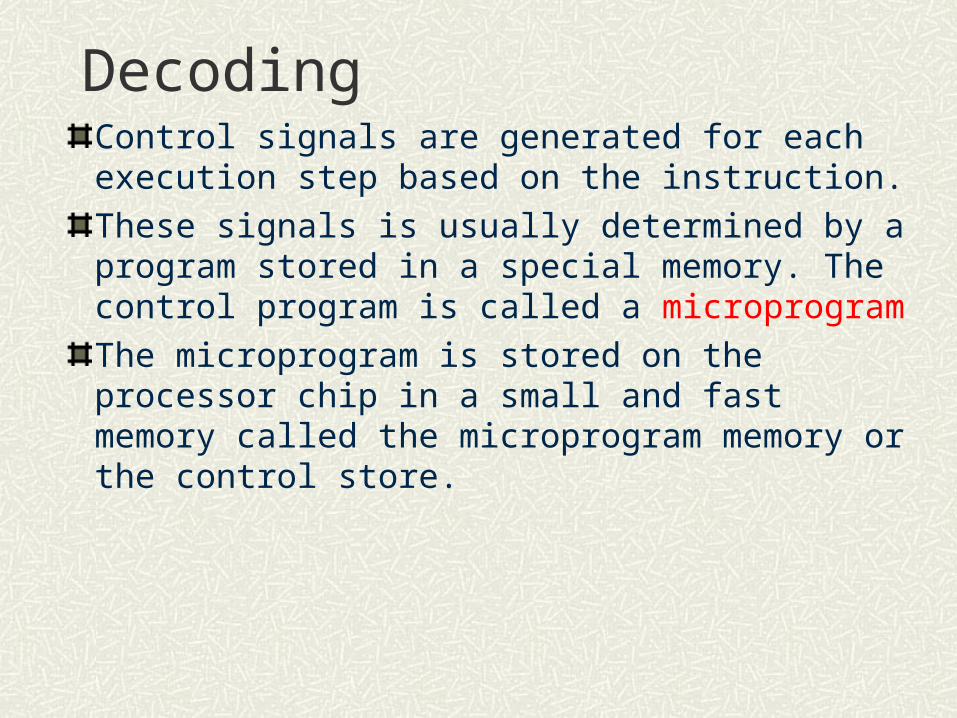
DecodingControl signals are generated for each execution step based on the instruction.
These signals is usually determined by a program stored in a special memory. The control program is called a microprogram
The microprogram is stored on the processor chip in a small and fast memory called the microprogram memory or the control store.
Decoding

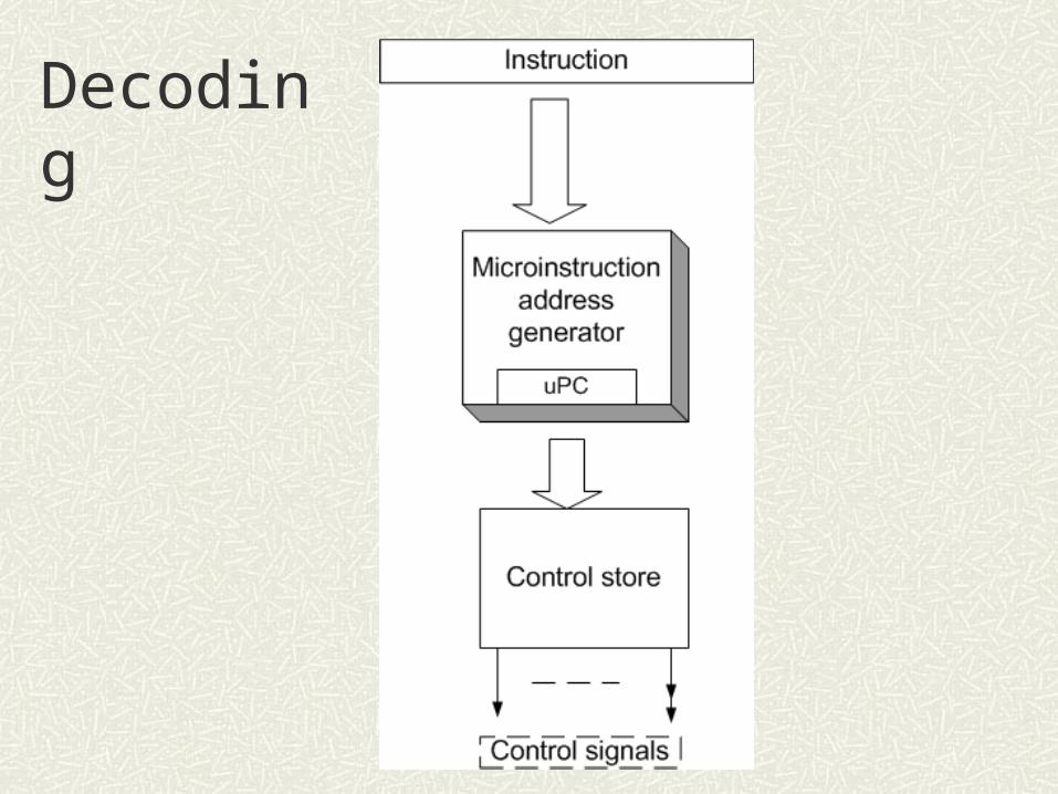
DecodingMicroprogrammed control consists of a microinstruction address generator, which generates the address to be used for reading microinstructions from the control store.
The address generator uses a microprogram counter, uPC, to keep track of control store addresses when reading microinstructions from successive locations.
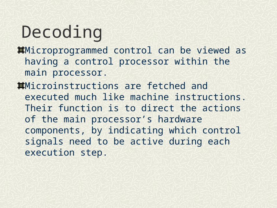
DecodingMicroprogrammed control can be viewed as having a control processor within the main processor.
Microinstructions are fetched and executed much like machine instructions. Their function is to direct the actions of the main processor’s hardware components, by indicating which control signals need to be active during each execution step.
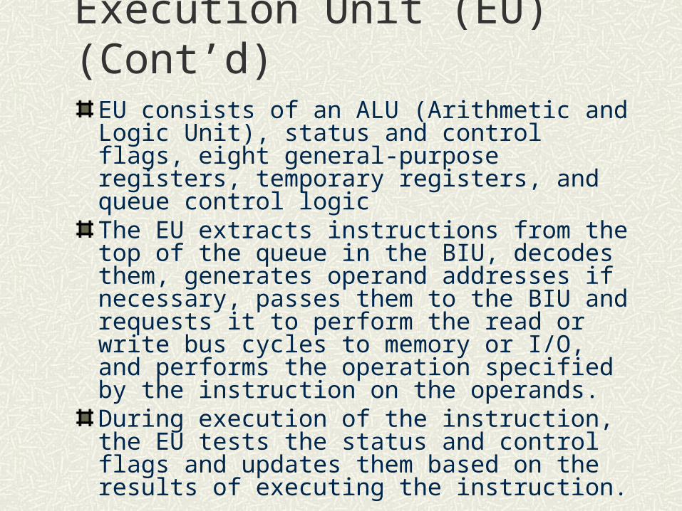
Execution Unit (EU) (Cont’d)EU consists of an ALU (Arithmetic and Logic Unit), status and control flags, eight general-purpose registers, temporary registers, and queue control logic The EU extracts instructions from the top of the queue in the BIU, decodes them, generates operand addresses if necessary, passes them to the BIU and requests it to perform the read or write bus cycles to memory or I/O, and performs the operation specified by the instruction on the operands. During execution of the instruction, the EU tests the status and control flags and updates them based on the results of executing the instruction.

Functions of EU
ADD AX, 16 ; meaning add 16 to AXWhere AX is a register inside the CPUIf AX is 20 then after the operation it becomes 36For the above operation, do we need to fetch operand from memory?16 in the above operation is called an immediateImmediate values are stored as part of an instruction and fetched together with the instructionNow if it is ADD AX, X ; X is a variableDo we need to fetch the operand X from memory?

Functions of EUIf the instruction queue is empty, the EU waits for the next instruction byte to be fetched and shifted to the top of the queue.
When the EU executes a branch or jump instruction, it transfers control to a location corresponding to another set of sequential instructions. Whenever this happens, the BIU automatically resets the queue and then begins to fetch instructions from this new location to refill the queue.

Jump and branch

Summary
What is the pre-fetch concept?
What is a pipeline and its advantage?
What are functions performed by the BIU and EU
What is a multiplexed address/data bus
What is the segment concept
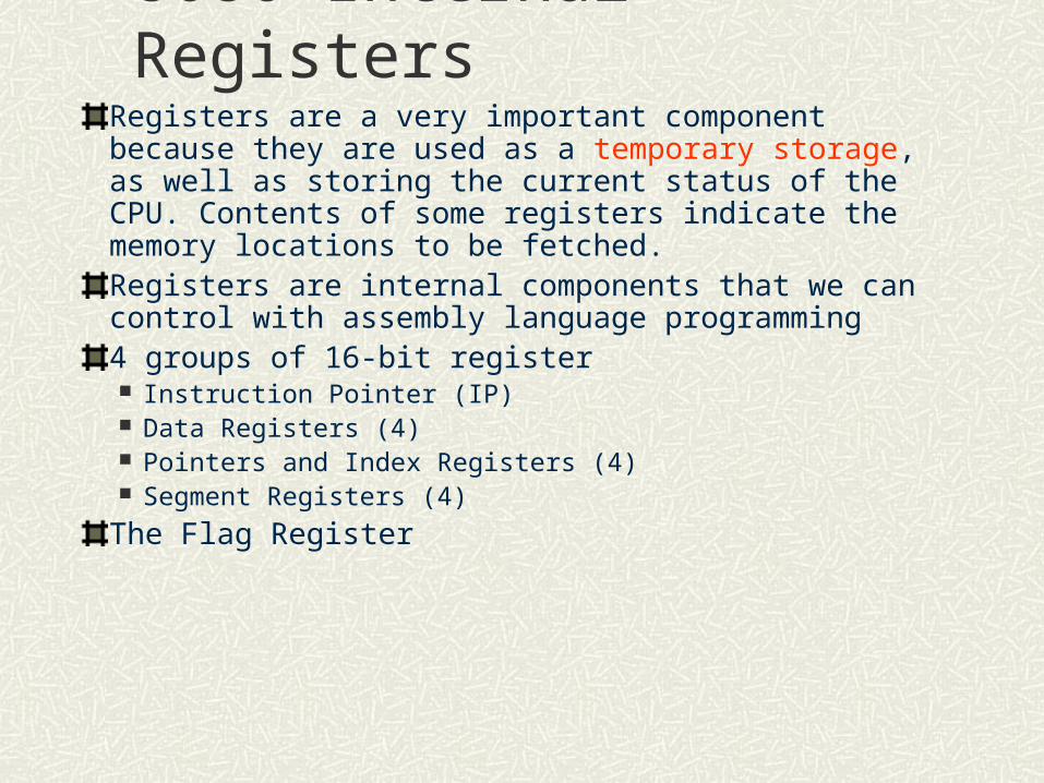
8086 Internal RegistersRegisters are a very important component because they are used as a temporary storage, as well as storing the current status of the CPU. Contents of some registers indicate the memory locations to be fetched.Registers are internal components that we can control with assembly language programming4 groups of 16-bit register Instruction Pointer (IP) Data Registers (4) Pointers and Index Registers (4) Segment Registers (4)
The Flag Register
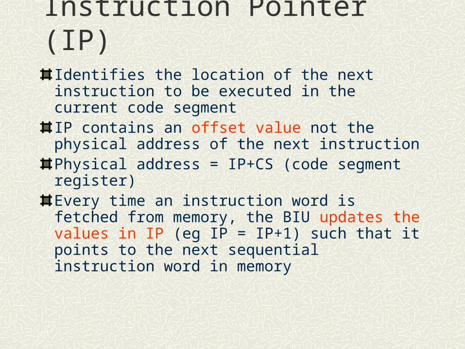
Instruction Pointer (IP)Identifies the location of the next instruction to be executed in the current code segmentIP contains an offset value not the physical address of the next instruction Physical address = IP+CS (code segment register)Every time an instruction word is fetched from memory, the BIU updates the values in IP (eg IP = IP+1) such that it points to the next sequential instruction word in memory

Data Registers
4 general purpose data registers and are used for temporary storage of frequently used intermediate results. This can improve the speed (why???)Register can use either as 8-bit or 16-bitAccumulator Register (AX: AH AL)Base Register (BX: BH BL)Count Register (CX: CH CL)Data Register (DX: DH DL)
AX (16-bit)
AH (8-bit) AL (8-bit)

Data RegistersThe general purpose data registers can be used for arithmetic or logic operations For example, to carry out an addition: add ax, bxThe result is stored in ax and it is equal to the sum of values in ax and bx (in C, it is similar to ax+=bx)For string instruction, the CX register is used to store a count value representing the number of bytes to be movedAll I/O operations require data that are to be input or output to be in the A register, while register DX holds the address of the I/O port

Segment RegistersThe segment registers are used for accessing the memoryThe 8086 address space is segmented into 64K-byte segments and just four segments can be active at a time.In theory, how many segments can we have???? The segment registers are used to select the active segments
Code Segment (CS) Register CS identifies the starting address of the 64-K byte segment
known as the code segment. Code segments of memory contain instructions of the program.
Data Segment (DS) Register DS register identifies the starting location of the current data
segment in memory. Data is stored in the data segment.

Segment Registers (Cont’d)
Stack Segment (SS) Register SS register contains a logical address that identifies the
starting location of the current stack segment in memory. Stack is used for temporary storage
Extra Segment (ES) Register ES register identifies the extra segment usually used for
data storage.
The segment registers store the base address of a segment. To determine the physical address, an offset is required. The index registers are used to store the offset value.

Pointer and Index RegistersStack Pointer (SP) – permits easy access to locations in the stack segment of memory The value in SP represents the offset of the next stack
location which can be accessed relative to the current address in the stack segment (SS) register, i.e., always points to the top of the stack.
Base Pointer (BP) BP represents an offset from the SS register. However, it is
used to access data within the stack segment. Used in the based addressing modeThe applications of the various registers will be discussed in
details when we learn assembly language programming
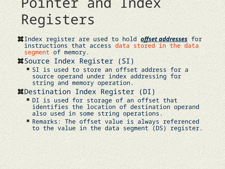
Pointer and Index RegistersIndex register are used to hold offset addresses for instructions that access data stored in the data segment of memory.
Source Index Register (SI) SI is used to store an offset address for a source operand
under index addressing for string and memory operation.
Destination Index Register (DI) DI is used for storage of an offset that identifies the location
of destination operand also used in some string operations. Remarks: The offset value is always referenced to the value
in the data segment (DS) register.
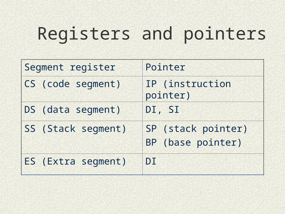
Registers and pointers
Segment register Pointer
CS (code segment) IP (instruction pointer)
DS (data segment) DI, SI
SS (Stack segment) SP (stack pointer)
BP (base pointer)
ES (Extra segment) DI

Flag Register
The flag register is a 16-bit register within the execution unit. The status flags in the register indicate conditions that are produced as the result of executing an arithmetic or logic instruction.
What kind of conditions can you think of???

8086 Flag Register (status flag)C - Carry Bit (set if there is a carryout or borrowin)P - Parity Bit (set if lower byte of the result contains even number of 1s) – odd parityZ - Zero Bit (set if result after an operation is equal to zero)S - Sign Bit (represent negative value produced during an operation)O - Overflow Bit (result is out of range). If the result of a signed operation is not large enough to be accommodated in a destination register. When an overflow will occur? Give one exampleThe above are the most commonly used flag registers, there are others but not discussed in this subject!!!!!!
Example
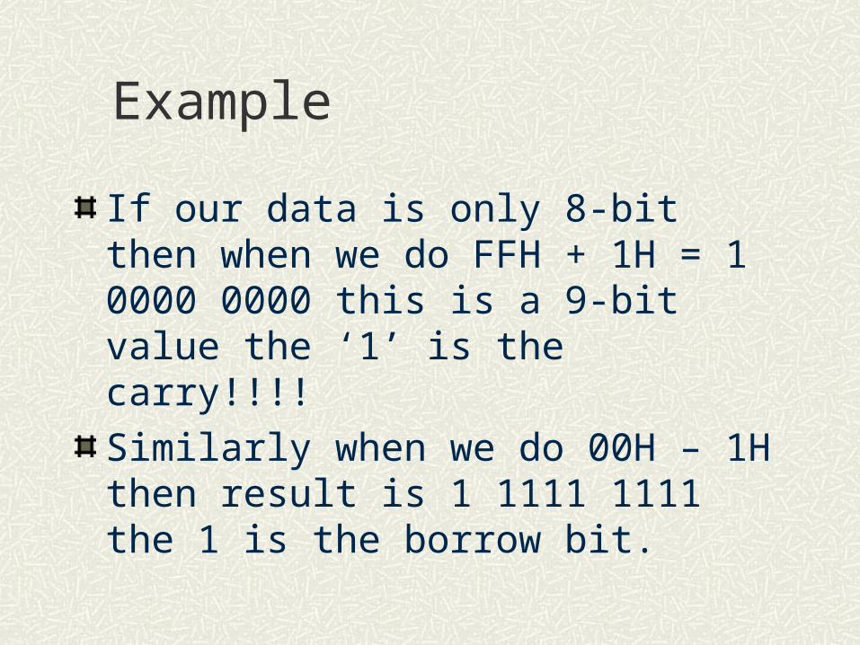
If our data is only 8-bit then when we do FFH + 1H = 1 0000 0000 this is a 9-bit value the ‘1’ is the carry!!!!
Similarly when we do 00H – 1H then result is 1 1111 1111 the 1 is the borrow bit.

Flags
consider using 8-bit values A and B, determine flag status for C, S, Z and O If A = 0FH, B = 1; A+B If A = 0, B = 1; A-B If A = 7FH, B = 1; A+B If A = 80, B = 0F; A-B If A = FFH, B = 1; A+B If A = 2FH, B = 60, C = -1; (A+C) -B
Block diagram for a simple computer system
CPUmemory
Display unit LCD
I/O
Get instruction from memory Perform operation Get next instruction

Bus Cycle
Bus – address and data
Bus cycle is used to access memory, I/O devices, or the interrupt controller.
Bus cycle starts with an address being output on the system bus followed by a read or write data transfer.
A series of control signals are produced to control the direction and timing of the bus
A standard bus cycle consists of 4 clock periods
Understand system bus timing will assist you to choose the proper memory device

Bus cycleT1 : BIU puts an address on the bus
T2: data are put on the bus (for write cycle)
T2: bus in High Z mode (for read cycle)
T3: data on the bus
T4: data on the bus
For a 5MHz system, how long does it take to complete 1 bus cycle????

Read cycle

Write cycle

Wait states
Wait states can be inserted into a bus cycle
In response to request by an event in external hardware
READY input of 8086 is set LOW
As long as READY is held low, wait states (Tw) are inserted between T3 and T4
For a write cycle, data maintained on the bus
Purpose: to extend the duration of the bus cycle, so slower memory devices can be used

Bus cycle

Example
Assembly Language Machine Code
MOV AX, 0F802H B802F8
PUSH AX 50
MOV CX, BX 8BCB
MOV DX, CX 8BD1
ADD AX, [SI] 0304
ADD SI, 8086H 81C68680
JMP $ -14 EBF0

Instruction sequence

Instruction sequence
B802
02F850

Instruction sequence

Pins definition
AD15 – AD0 Address/Data BusA19/S6 – A16/S3- Address/StatusBHE/S7 – Bus high enableMN/MX – min. max. mode controlRD – read control (read data from memory or I/O)Test – wait on test (input). If test signal is HIGH then processor will be in an idle stateReady – (input) wait state controlReset – system reset (if kept HIGH for 4 clock cycles)NMI – non-maskable interrupt requestINTR – interrrupt requestCLK – system clock
Pins definition
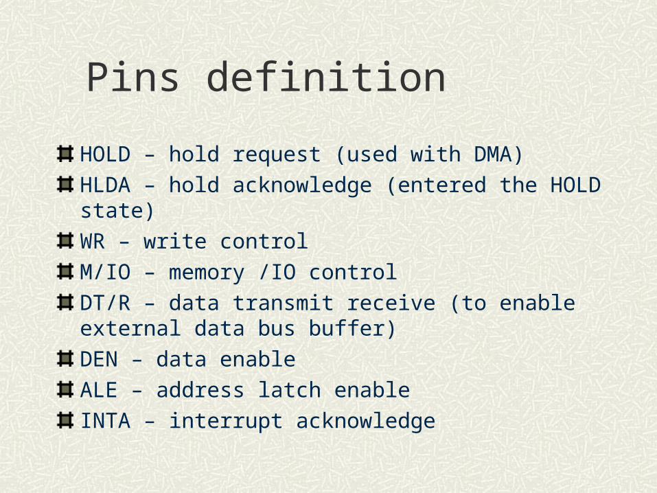
HOLD – hold request (used with DMA)
HLDA – hold acknowledge (entered the HOLD state)
WR – write control
M/IO – memory /IO control
DT/R – data transmit receive (to enable external data bus buffer)
DEN – data enable
ALE – address latch enable
INTA – interrupt acknowledge
Pins definition
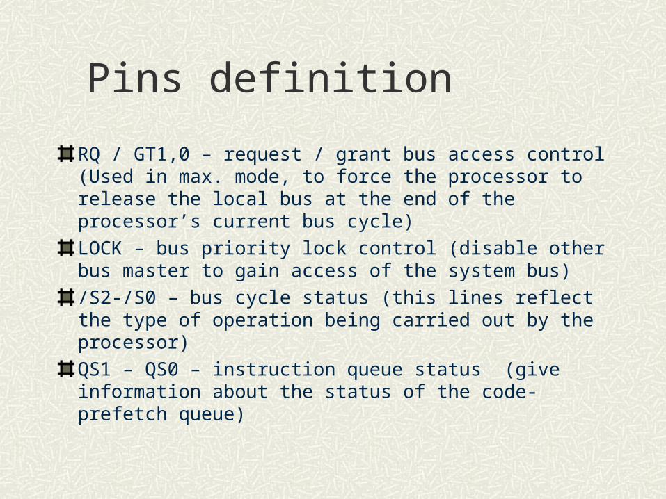
RQ / GT1,0 – request / grant bus access control (Used in max. mode, to force the processor to release the local bus at the end of the processor’s current bus cycle)
LOCK – bus priority lock control (disable other bus master to gain access of the system bus)
/S2-/S0 – bus cycle status (this lines reflect the type of operation being carried out by the processor)
QS1 – QS0 – instruction queue status (give information about the status of the code-prefetch queue)

Status lines – reflects activities of the BIU/S2 /S1 /S0 Indication
0 0 0 Interrupt acknowledge
0 0 1 Read I/O port
0 1 0 Write I/O port
0 1 1 Halt
1 0 0 Code access
1 0 1 Read memory
1 1 0 Write memory
1 1 1 passive

Instruction Queue status
QS1 QS0 Indication
0 0 No operation
0 1 First byte of opcode from the queue
1 0 Empty queue
1 1 Subsequent byte from the queue

Instruction sequence
B802
02F850
100
10

Status signals
S6 – S3 – are output on the bus at the same time that data are transferred over the other bus lines
S4 and S3 form a 2-bit binary code that identifies which of the 8086’s internal segment register was used to generate the physical address
00 – extra 01 – stack 10 – code/none 11 – Data
S5 – logic level of the interrupt enable flag
S6 – not used always at 0
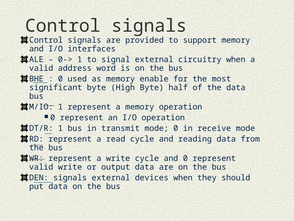
Control signalsControl signals are provided to support memory and I/O interfacesALE – 0-> 1 to signal external circuitry when a valid address word is on the busBHE : 0 used as memory enable for the most significant byte (High Byte) half of the data bus M/IO: 1 represent a memory operation
0 represent an I/O operationDT/R: 1 bus in transmit mode; 0 in receive modeRD: represent a read cycle and reading data from the busWR: represent a write cycle and 0 represent valid write or output data are on the busDEN: signals external devices when they should put data on the bus

Operating modes of 8086The 8086 can run in two different modes: minimum and maximum
In min. mode 8086 provides all the control signals needed to implement the memory I/O interfaces
In max. mode, it provides signals (status signals) for implementing a multiprocessor/coprocessor system environment
In max. mode, bus controller, bus arbiter are included in the system. The controller derives the control signals based on the status signals
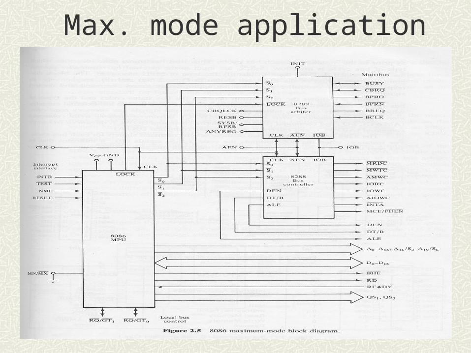
Max. mode application
Maximum mode
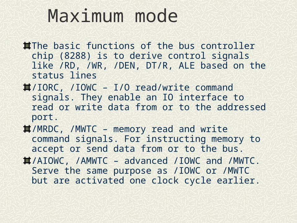
The basic functions of the bus controller chip (8288) is to derive control signals like /RD, /WR, /DEN, DT/R, ALE based on the status lines/IORC, /IOWC – I/O read/write command signals. They enable an IO interface to read or write data from or to the addressed port./MRDC, /MWTC – memory read and write command signals. For instructing memory to accept or send data from or to the bus. /AIOWC, /AMWTC – advanced /IOWC and /MWTC. Serve the same purpose as /IOWC or /MWTC but are activated one clock cycle earlier.
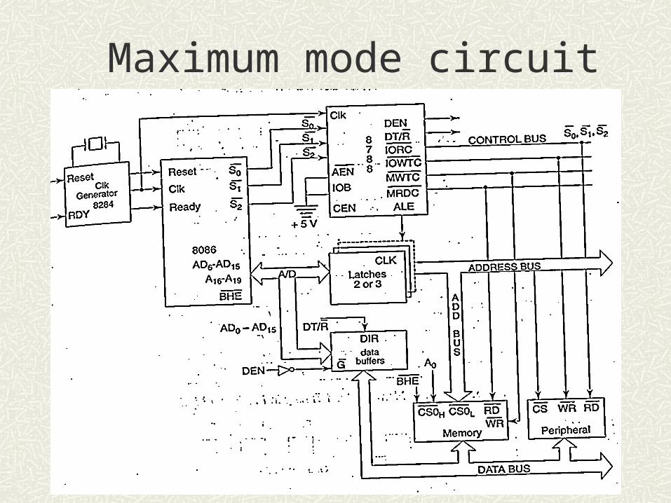
Maximum mode circuit
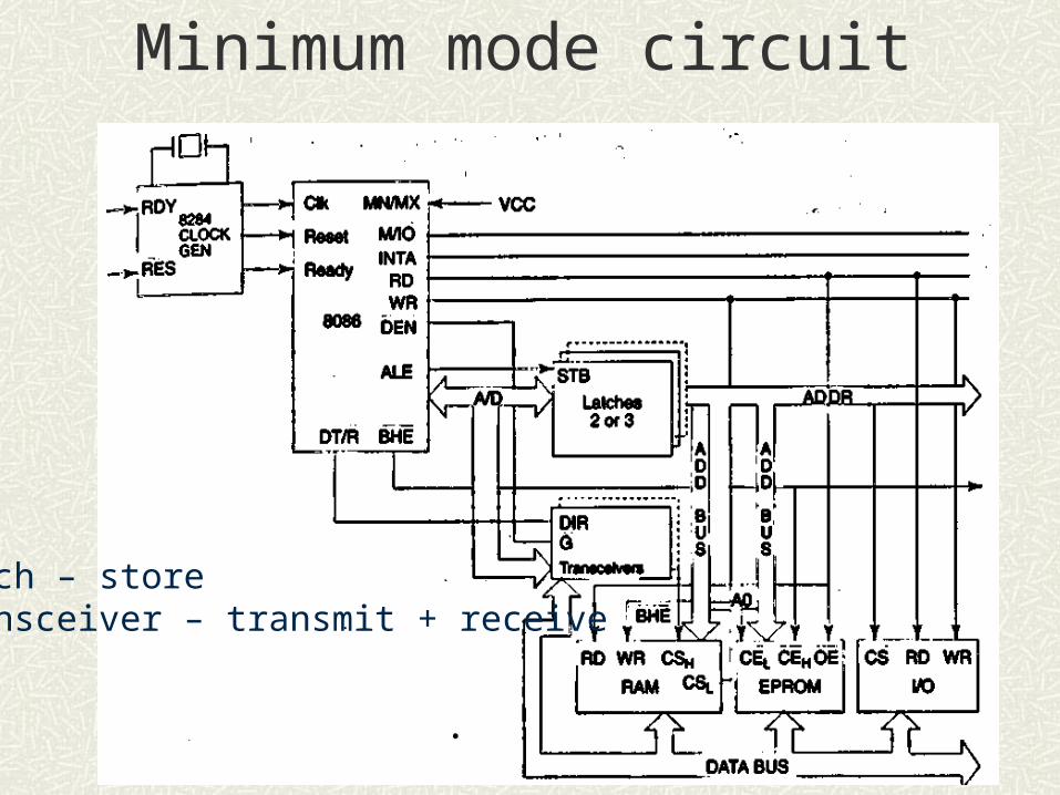
Minimum mode circuit
Latch – storeTransceiver – transmit + receive

Read cycleWhy there are two address?
Output From address latch
Output from multiplexed Address/data bus

Memory
memory
Address
Data
To access the memory both address and data must be availableat the same time. But for 8086, the bus is multiplexed so Physically it is not possible to supply both information simultaneously
So address latches areused to hold the addressinformation when the busis used to transceive data
Modern microprocessor architecture
Based on your understanding of the 8086 microprocessor,what features of the 8086 are needed to be modified in order to make it more powerful?
What are the major differences between a modern microprocessor and a 8086???

Modern microprocessors
The following features are crucial to the performance: Operating speed (clock rate) Memory (size and speed) Data size Floating point processing Overlapping of execution and memory access Perform more tasks in a single cycle

Modern microprocessorOperating speed The 8086 operates at 5MHz The latest Intel microprocessor (i5, i7, i9) can operate at
the 2.6GHz range The operating frequency is governed by the fabrication
techniques (0.13 Micron technology for P4 and the 8086 is based on 3 Micron technology). With sub-micron technology we can put more components into the chip
The higher the operating speed, more heat will be generated and cooling the CPU becomes more important. No cooling is for the CPU is required in the 486 era
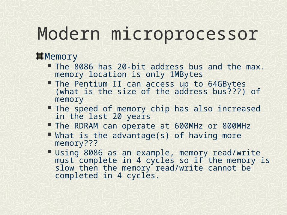
Modern microprocessorMemory The 8086 has 20-bit address bus and the max. memory
location is only 1MBytes The Pentium II can access up to 64GBytes (what is the
size of the address bus???) of memory The speed of memory chip has also increased in the last
20 years The RDRAM can operate at 600MHz or 800MHz What is the advantage(s) of having more memory??? Using 8086 as an example, memory read/write must
complete in 4 cycles so if the memory is slow then the memory read/write cannot be completed in 4 cycles.

Memory speed
To improve the performance, internal high-speed memory is provided for the storage of data as well as instruction. These internal memory is called cache
There are cache inside the CPU and it is called Level 1 (L1) cache (there are at least 8Kb in P4)
The cache located between the CPU and the external memory is called Level 2 (L2) cache (speed of cache is higher then the traditional memory) (512K in P4)
In newer microprocessors design, L2 cache is also located inside the CPU so therefore, L3 cache is also provided. L3 cache is external just like L2 cache in the old days.
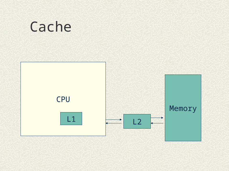
Cache
CPU
L1 L2
Memory
Cache
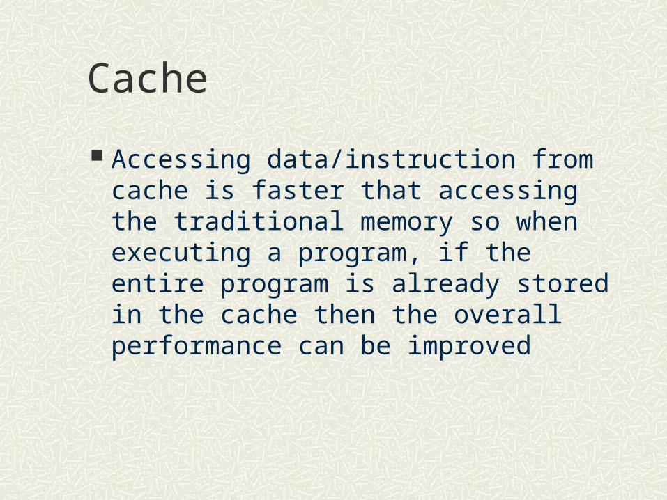
Accessing data/instruction from cache is faster that accessing the traditional memory so when executing a program, if the entire program is already stored in the cache then the overall performance can be improved
Cache
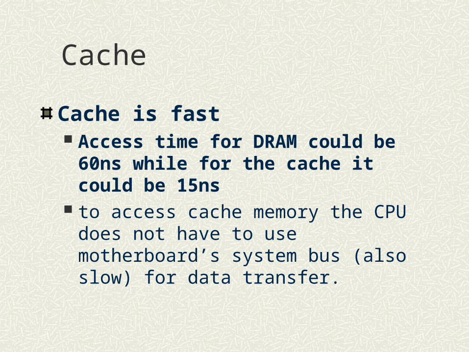
Cache is fast Access time for DRAM could be 60ns while
for the cache it could be 15ns to access cache memory the CPU does not have
to use motherboard’s system bus (also slow) for data transfer.

Why Cache?The effectiveness of cache is based on a property of computer program called locality of reference.
Most of a program’s execution time is spent in routines in which many instructions are executed repeatedly, such as looping, functions etc.
Cache
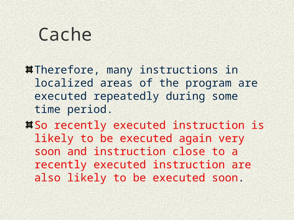
Therefore, many instructions in localized areas of the program are executed repeatedly during some time period.
So recently executed instruction is likely to be executed again very soon and instruction close to a recently executed instruction are also likely to be executed soon.

CacheWhenever an information item (data or instruction) is first needed, this item should be brought to the cache because it is likely to be needed again soon.
Instead of fetching just one item from the main memory it is useful to fetch several items that are located at adjacent addresses as well.

CacheThe cache is usually divided into smaller units, called blocks, lines or slots. In 486, the 8K cache is divided into 4 2K blocks. Each block is 16bytes x 128 rowsThe 16-byte row is divided into 4-byte lines. Any of the 4 lines cannot be accessed partially.During operations, the microprocessor always check the cache for data and instruction first. If data is already stored in the cache – it is called a cache hitUsually a mechanism called paging is employed to write frequently used data and instruction into the cacheIf the data is not found then – cache miss

Operation of cacheThe processor does not need to know the existence of the cache. It simply issues Read and Write requests using addresses that refer to locations in the memory.
The cache control circuitry determines whether the requested word currently exists in the cache. If it does, the Read or Write operation is performed on the appropriate cache location.
This is called a cache hit. The main memory is not involved when there is a cache hit in a Read operation. For a write operation, there two techniques: write-through and write-back.
Cache write In a write-through, both the cache and the main memory are updated. In write-back, only the cache location is updated and a flag (a dirty or modified bit) is used to reflect the change in status. The main memory location is updated later, when the block containing this marked word is removed from the cache to make room for a new block.

Cache structureIn order to identify if data from main memory is stored in a cache slot, a tag is provided.
A tag contains information related to the address of the memory being stored in the cache.
The size of the tag is address bus size – lg N where N is the number of bytes in the data part of the cache slot. For example if the address bus is 20 bits and the cache slot is 32 bytes then the tag is 20-5 = 15 bits.
If the memory data is stored in the cache then the upper 15 bits of the address should map with the tag value of the cache.

Structure of cache
If the tag is 091AH then that means the memory addresses 12340H to1235FH are stored in the cache (if the cache block is 32 bytes)

Cache structureThe V bit is the valid bit indicating whether the slot holds valid date. If V=1, then the data is valid. If V=0, then data is not valid. Initially, it is invalid. Once data is placed in the slot it is valid.
The D bit is the dirty bit. This bit only has meaning if V=1. This indicates that the data in the slot has been modified (written to) or not. If D=1, data has been modified since being in the cache. If D=0, then the data is the same as it was when it first entered the cache.
Mapping between the cache and external memory
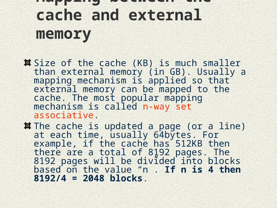
Size of the cache (KB) is much smaller than external memory (in GB). Usually a mapping mechanism is applied so that external memory can be mapped to the cache. The most popular mapping mechanism is called n-way set associative. The cache is updated a page (or a line) at each time, usually 64bytes. For example, if the cache has 512KB then there are a total of 8192 pages. The 8192 pages will be divided into blocks based on the value “n”. If n is 4 then 8192/4 = 2048 blocks.

Mapping between the cache and external memory
Based on the number of blocks, the external memory will also be divided into the same number of blocks. For example, if the external memory is 1GBytes then each block of the external memory is equal to 512Kbytes. (1G = 230) and each block of the external memory will be mapped to 1 block of the cache. So every 4 lines of the cache will be in charge (used to store) of 512Kbytes of the external memory.
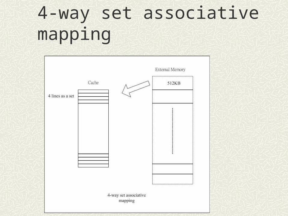
4-way set associative mapping

Example of 4 way set associativeIf the CPU has a 32-bit address and the cache is 128 slot and 32 bytes per slot. Using 8-way set associative then 8 slots per set, there should be 16 sets (128/8). The tag size of each cache slot is 32 – 5 = 27 bits.
Since the cache is now divided into sets so 4 bits are needed to represent the set number.
Tag (27-4 = 23 bits) & Set 4 bits
The memory address is 32 bits and interpreted in the following:
Tag (23 bits) +Set 4 bits + Offset (5 bits)

Example
If address issued is 12345678H (32-bit)
If the cache slot is 32 bytes
Then the set number from the above is 3
And tag number is 091A2BH

Replacement algorithmsWhen a new block is to be brought into the cache and all the positions that it may occupy are full, the cache controller must decide which of the old blocks to overwrite.
It should keep blocks in the cache that are likely to be reference in the near future.
A direct approach is to overwrite the one that has gone the longest time without being referenced. This block is called the least recently used (LRU) block, and this is called the LRU replacement algorithm. The cache controller must track references to all blocks as computation proceeds.

Modern Microprocessor
Data The 8086 has a 16-bit data bus The P4 has a 64-bit data bus so can get more
data in a single read/write cycle Or processing of high-precision data can be
more effective Consider this: what is the maximum value can
be represented by a 16-bit and a 32-bit pattern respectively
Overlapping of operations
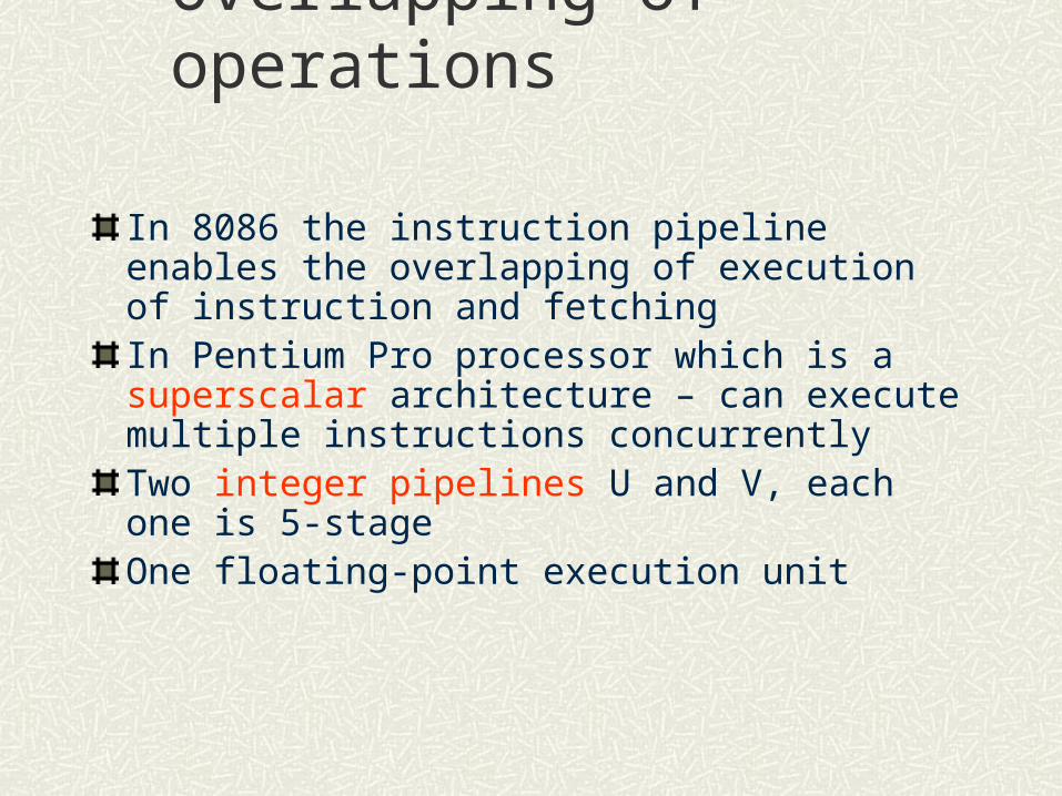
In 8086 the instruction pipeline enables the overlapping of execution of instruction and fetching In Pentium Pro processor which is a superscalar architecture – can execute multiple instructions concurrentlyTwo integer pipelines U and V, each one is 5-stageOne floating-point execution unit
Overlapping of operations
So it is possible to execute three instructions simultaneously (with proper programming the speedup can be up to 40%)
Pentium Processor
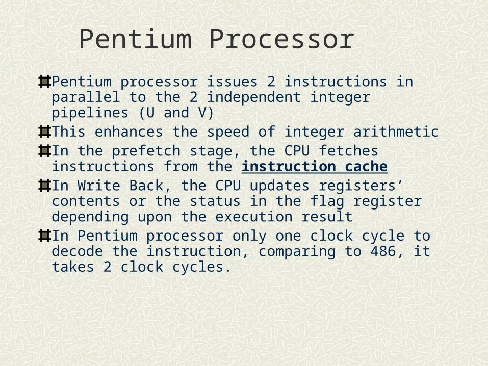
Pentium processor issues 2 instructions in parallel to the 2 independent integer pipelines (U and V)This enhances the speed of integer arithmetic In the prefetch stage, the CPU fetches instructions from the instruction cacheIn Write Back, the CPU updates registers’ contents or the status in the flag register depending upon the execution resultIn Pentium processor only one clock cycle to decode the instruction, comparing to 486, it takes 2 clock cycles.
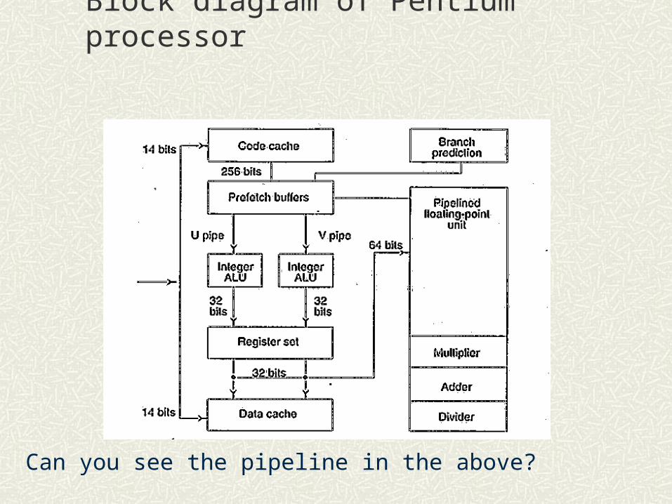
Block diagram of Pentium processor
Can you see the pipeline in the above?

Block diagram of U-V pipe for Pentium processor
The pipeline of 8086has how many stages?

The 8086 instruction execution sequence
Fetch instruction
Decode and determine operandaddress
Fetch operand
Execute
Basic operations performed by a CPU

Branch prediction As in 8086, when a “jump” operation is being performed then the instruction queue must be reset and therefore, instruction already pre-fetched is discarded.
If you can predict when a branch or jump instruction will take place then you can pre-fetch from the new “jump” point implying that the instructions being pre-fetched are always relevant to the instruction to be executed.

Branch prediction
The cache controller of modern CPUs analyze the memory block it loaded and whenever it finds a JMP instruction in there it will load the memory block for that position in the L2 memory cache before the CPU reaches that JMP instruction.
In a conditional statement such as if a =< b go to address 1, or if a > b go to address 2. This would make a cache miss, because the values of a and b are unknown and the cache controller would be looking only for JMP-like instructions.

Branch prediction
The cache controller loads both conditions into the memory cache. Later, when the CPU processes the branching instruction, it will simply discard the one that wasn’t chosen. It is better to load the memory cache with unnecessary data than directly accessing the RAM memory.
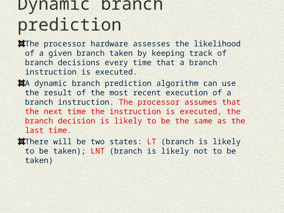
Dynamic branch predictionThe processor hardware assesses the likelihood of a given branch taken by keeping track of branch decisions every time that a branch instruction is executed.
A dynamic branch prediction algorithm can use the result of the most recent execution of a branch instruction. The processor assumes that the next time the instruction is executed, the branch decision is likely to be the same as the last time.
There will be two states: LT (branch is likely to be taken); LNT (branch is likely not to be taken)
Dynamic branch predictionSuppose it starts at LNT, when the branch instruction is executed and the branch is taken, the machine moves to state LT. Otherwise, it remains in state LNT. The next time the same instruction is encountered, the branch is predicted as taken if it is in state LT. Otherwise it is predicted as not taken.
Dynamic branch predictionOnce a loop is entered, the decision for the branch instruction that controls looping will always be the same except for the last pass through the loop.
Hence, each prediction for the branch instruction will be correct except in the last pass.
The prediction in the last pass will be incorrect, and the branch history state will be changed to the opposite state. Therefore, if the same loop is being executed again then the prediction will be wrong.

Dynamic branch prediction
LNT LT
BT
BT
BNT
BNT
Consider aDo {
}While (condition) loop

Enhanced dynamic branch prediction
SNT LNT
BT
BNT
LT ST BT
BNT
BT
BNT
BNT BT
ST – strongly likely to be takenSNT – strongly likely not tobe taken

Modern microprocessor
Floating point hardware
Do you know how floating-point number is represented in a computer?
The floating-point hardware is an important design feature in modern processor
No floating-point hardware is available for 8086
For Intel, the co-processor mechanism was used until the emerge of the 486 microprocessors
Perform more tasks in a single cycle
MMX – multimedia extension It is for improving 2-D , 3-D multimedia applicationsUsing MMX instruction set, eight image elements (8-bit) can be loaded simultaneously and perform concurrent operation on themThe MMX instruction makes use of the 64-bit registers (the mantissa portion of the floating-point registers)MMX instructions are mainly integer operations
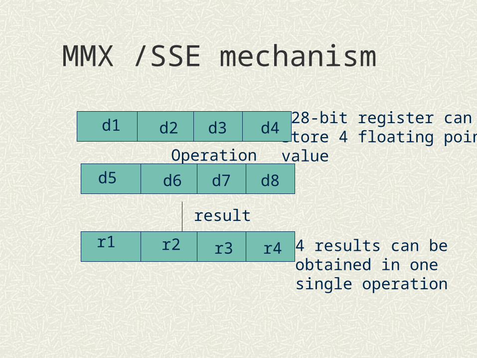
MMX /SSE mechanism
128-bit register can Store 4 floating point value
result
Operation
4 results can be obtained in onesingle operation
d1
d5
r1
d2 d3 d4
d6 d7 d8
r2 r3 r4
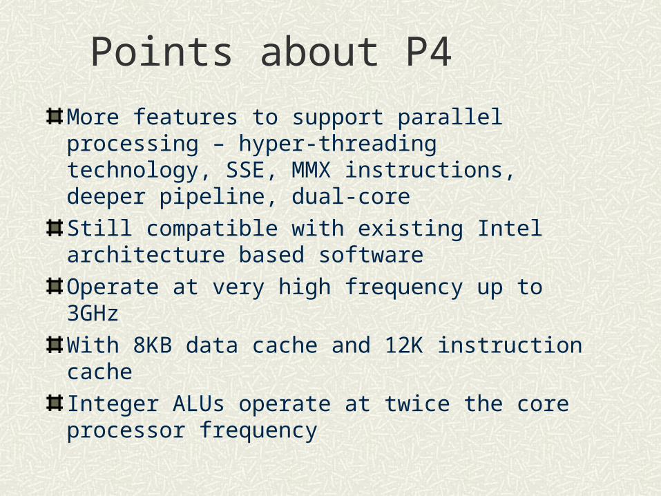
Points about P4
More features to support parallel processing – hyper-threading technology, SSE, MMX instructions, deeper pipeline, dual-core
Still compatible with existing Intel architecture based software
Operate at very high frequency up to 3GHz
With 8KB data cache and 12K instruction cache
Integer ALUs operate at twice the core processor frequency
Self-test
How to make a microprocessor to become more powerful!What is the most important hardware feature embedded in a 8086 microprocessor?What are the basic operations being performed when a computer is running?What is the maximum value represented by a 20-bit pattern?What is the maximum value represented by the sum of two 16-bit pattern?What is the major function of a ALU?What is the major functions of a BIU?Can you use a block diagram to represent a memory?What is an instruction pipeline and why it can improve the overall performance of a microprocessor?

Block diagram of Intel P4 CPU
Can you spot anyfeatures come fromthe 8086 ?

Introduction to microcontroller
If you want to develop a simple robot are you going to use a P5 microprocessor in your system?Usually to implement a simple system, microcontroller is used instead of a microprocessor. A microcontroller can be regarded as an all-in-one device with a CPU, memory, Input/Output interfaces all included in a single package. Commonly used microcontrollers include the 8051 series, Basic Stamp, BasicX etc. In addition, the cost of a microcontroller is usually lower than the traditional microprocessor, for example an 8051 is only HKD25.

MicrocontrollerSome microcontrollers also come with additional features such as ADC (analog to digital converter), DAC (digital to analog converter) and PWM (pulse-width modulation) output. All those features are very useful for the implementation of basic robotic or control systems.

The ADuC832 device
The ADuC832 is a powerful microcontroller and is being used in the experimental setup. Basic features of the device include:
8-channel 12-bit ADC 2 12-bit DAC 62Kbytes Program memory, 4kBytes data memory 2304 bytes on-chip data RAM dual PWM output (the PWM can be used to control
an analog device) 8051 compatible instruction set 4 8-bit Input/Output ports
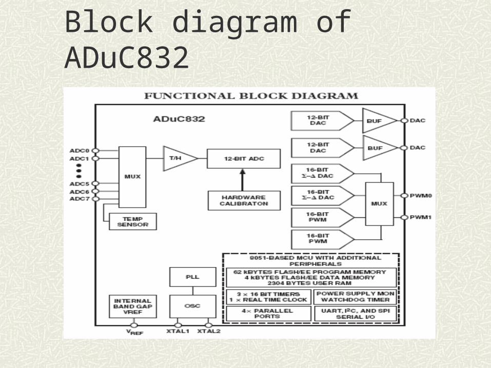
Block diagram of ADuC832

Application using microcontroller
The components can be connected directly to the microcontroller via the I/O ports without other supporting devices.
Sensor
ADuC832
Motor Motor