eecs 150 - components and design techniques for digital systems lec 20 – putting it together case...
TRANSCRIPT
EECS 150 - Components and Design Techniques for Digital Systems
Lec 20 – Putting it together
Case Study: A Serial Line Transmitter/Receiver
11-4-04
Stan BaekElectrical Engineering and Computer Sciences
University of California, Berkeley
Outline
• A Serial Line Transmitter/Receiver– Designing hardware to communicate over a single wire.
– The data will be sent serially
– The clocks on the two ends are completely asynchronous.
– Communication protocol – RS232
Motivation
• Data Transmission in asynchronous circuits– Handshaking
– Oversampling
• Design techniques– Timing diagram
– Top-down design
– Bubble-and-arc
• Communication Protocol – RS232– one of the most heavily used standards ever developed
for computing equipment.
– Baud rate: 9600 ~ 56000 bps
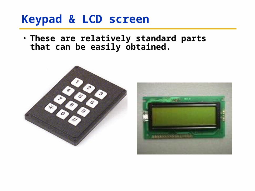
Keypad & LCD screen
• These are relatively standard parts that can be easily obtained.
Problem Specification (1)
• Our task is to design two devices
• The first one– Takes input from a telephone-like keypad.
– Sends a byte corresponding to the key over a single wire one bit at a time.
• The second one– Receives the serial data sent by the first one
– Displays it on a small LCD screen
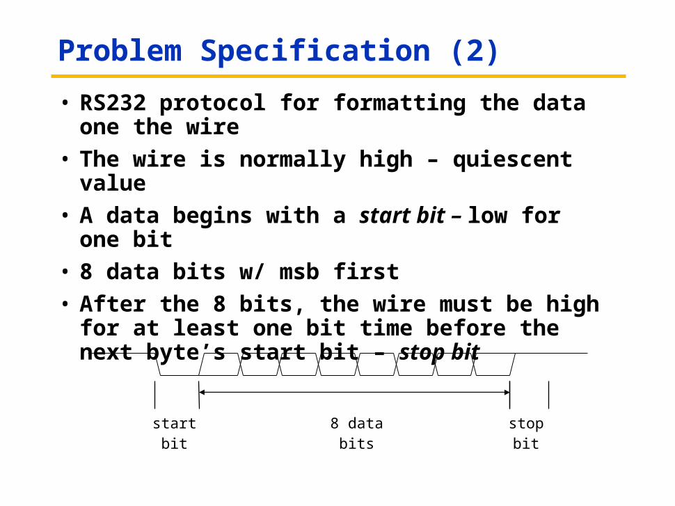
Problem Specification (2)
• RS232 protocol for formatting the data one the wire
• The wire is normally high – quiescent value
• A data begins with a start bit – low for one bit
• 8 data bits w/ msb first
• After the 8 bits, the wire must be high for at least one bit time before the next byte’s start bit – stop bit
8 databits
startbit
stopbit
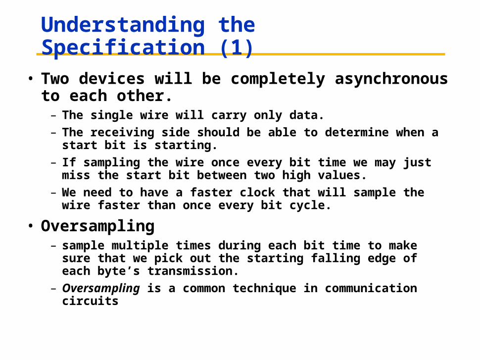
Understanding the Specification (1)
• Two devices will be completely asynchronous to each other.
– The single wire will carry only data.
– The receiving side should be able to determine when a start bit is starting.
– If sampling the wire once every bit time we may just miss the start bit between two high values.
– We need to have a faster clock that will sample the wire faster than once every bit cycle.
• Oversampling– sample multiple times during each bit time to make sure that we pick
out the starting falling edge of each byte’s transmission.
– Oversampling is a common technique in communication circuits
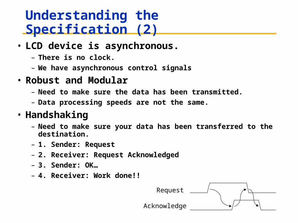
Understanding the Specification (2)
• LCD device is asynchronous.– There is no clock.
– We have asynchronous control signals
• Robust and Modular– Need to make sure the data has been transmitted.
– Data processing speeds are not the same.
• Handshaking– Need to make sure your data has been transferred to the destination.
– 1. Sender: Request
– 2. Receiver: Request Acknowledged
– 3. Sender: OK…
– 4. Receiver: Work done!!
Acknowledge
Request
Design Techniques
• Timing Diagram– Oversampling needs to pick up falling edge of input signal and
interacts with counters.
– Handshaking is between asynchronous circuits and synchronous circuits.
– In general, timing diagram is very important in digital design.
• Top Down & Bubble-and-arc Diagram– Top Down design: define larger block and break it into smaller
blocks.
– Bubble-and-arc for finite state machines.
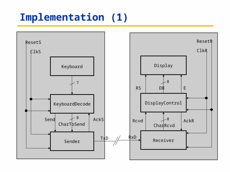
Implementation (1)
Receiver
DisplayControl
Display
8
ResetR
ClkR
RxD
Rcvd
DB
AckR
RS E
CharRcvd
8
Sender
Send 8
CharToSend
Keyboard
KeyboardDecode
7
ResetS
ClkS
TxD
AckS
• Sender – left side– Keyboard - input device
– KeyboardDecode – decodes the signals from the keypad and turn them in to the appropriate character code for the button
– Sender – takes the byte and serially transmits it over the single wire
• Receiver – right side– Display – LCD output
– DisplayControl – takes the data and control the LCD appropriately to get the corresponding character to show up on the screen.
– Reciever – observes the signal wire coming from the sender and determines when a byte has been received.
Implementation (2)
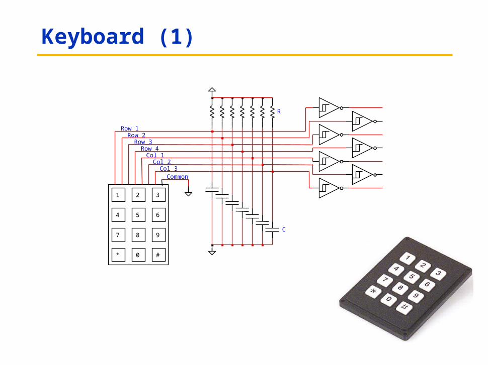
Keyboard (1)
1 2 3
4 5 6
7 8 9
0 #*
Common
Row 2
Row 4Col 1
Col 2Col 3
Row 1
Row 3
R
C
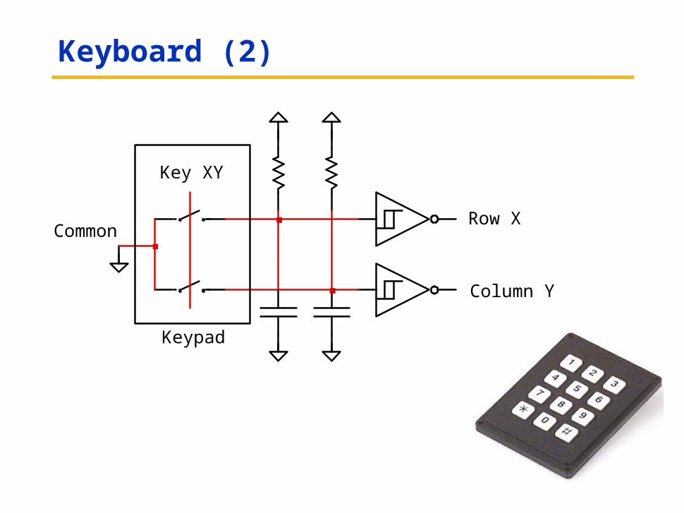
Keyboard (2)
Row X
Column Y
Key XY
Common
Keypad
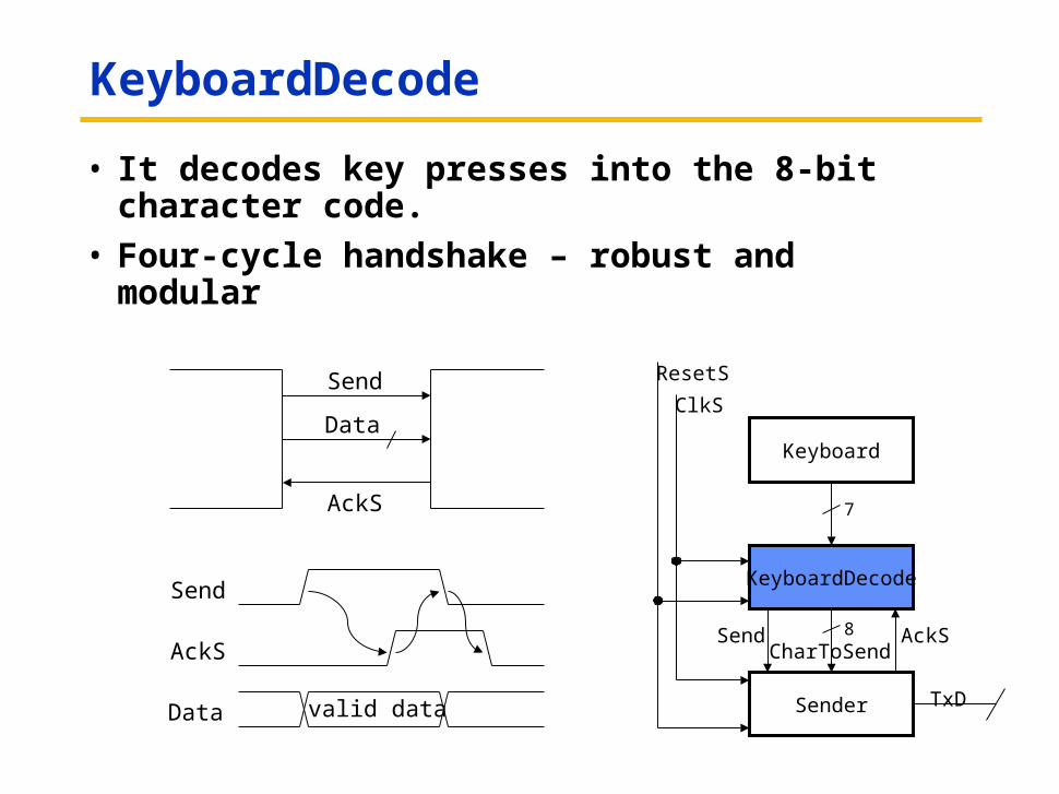
KeyboardDecode
• It decodes key presses into the 8-bit character code.
• Four-cycle handshake – robust and modular
valid dataData
AckS
Send
Send
AckS
Data
Sender
Send 8CharToSend
Keyboard
KeyboardDecode
7
ResetS
ClkS
TxD
AckS
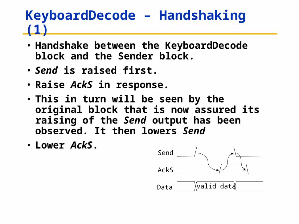
KeyboardDecode – Handshaking (1)
• Handshake between the KeyboardDecode block and the Sender block.
• Send is raised first.
• Raise AckS in response.
• This in turn will be seen by the original block that is now assured its raising of the Send output has been observed. It then lowers Send
• Lower AckS.
valid dataData
AckS
Send
KeyboardDecode – Handshaking (2)
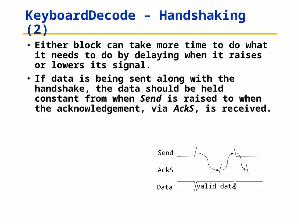
• Either block can take more time to do what it needs to do by delaying when it raises or lowers its signal.
• If data is being sent along with the handshake, the data should be held constant from when Send is raised to when the acknowledgement, via AckS, is received.
valid dataData
AckS
Send
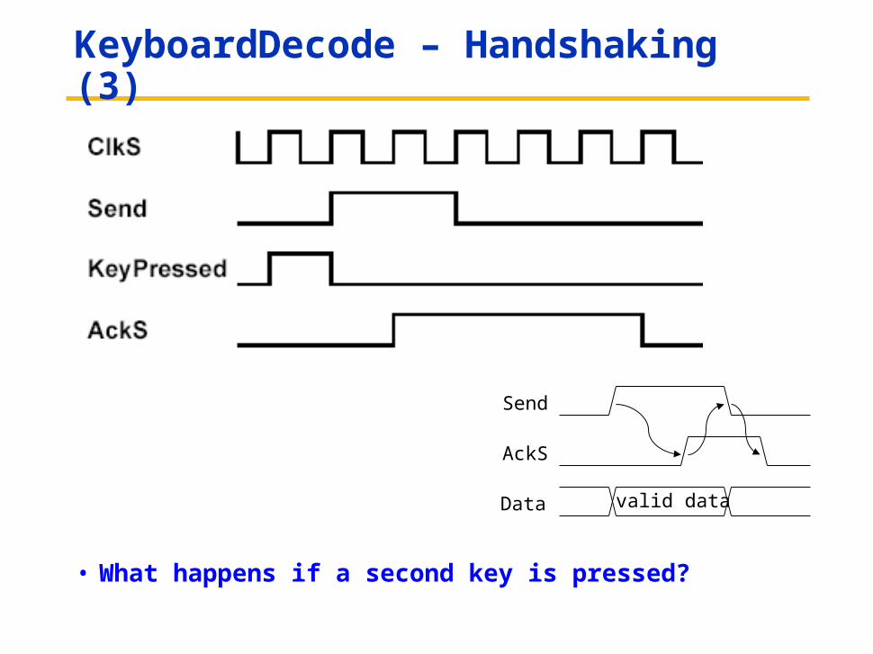
KeyboardDecode – Handshaking (3)
• What happens if a second key is pressed?
valid dataData
AckS
Send
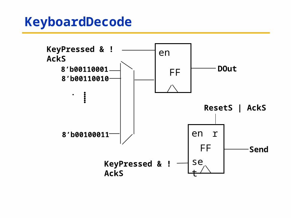
KeyboardDecode
FF
en
DOut
KeyPressed & !AckS
8’b001100018’b00110010
…….
8’b00100011
FF
en
Send
ResetS | AckS
KeyPressed & !AckS
r
set
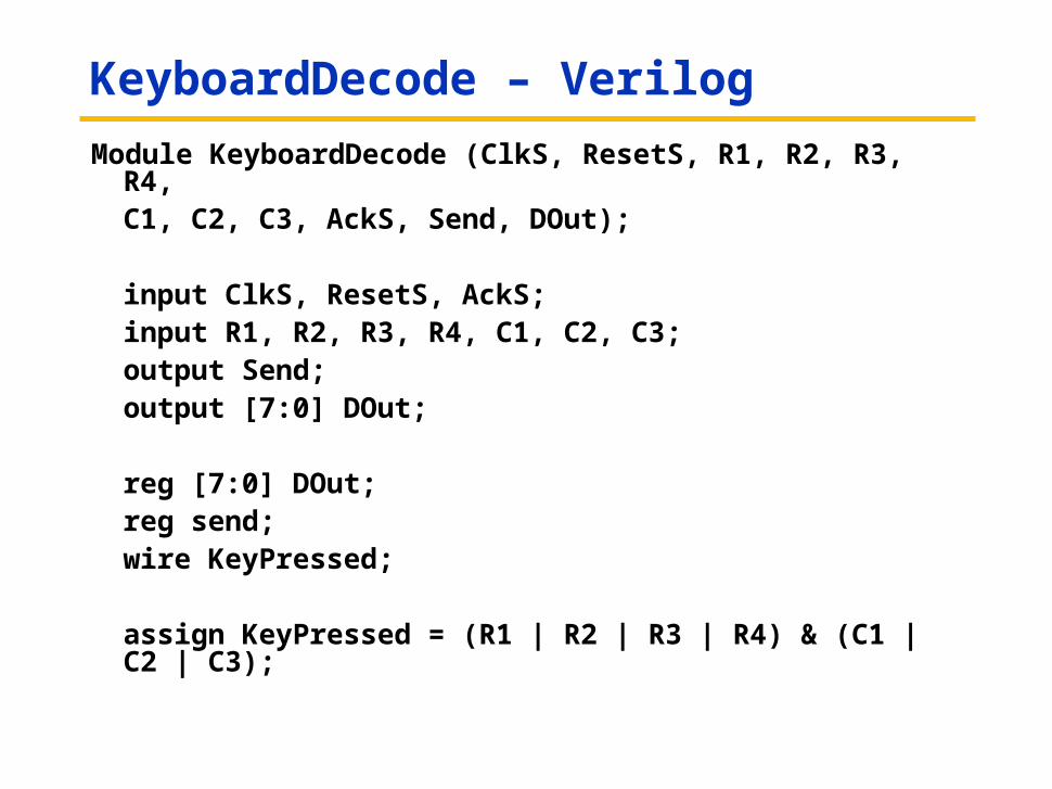
KeyboardDecode – Verilog
Module KeyboardDecode (ClkS, ResetS, R1, R2, R3, R4,C1, C2, C3, AckS, Send, DOut);
input ClkS, ResetS, AckS;input R1, R2, R3, R4, C1, C2, C3;output Send;output [7:0] DOut;
reg [7:0] DOut;reg send;wire KeyPressed;
assign KeyPressed = (R1 | R2 | R3 | R4) & (C1 | C2 | C3);
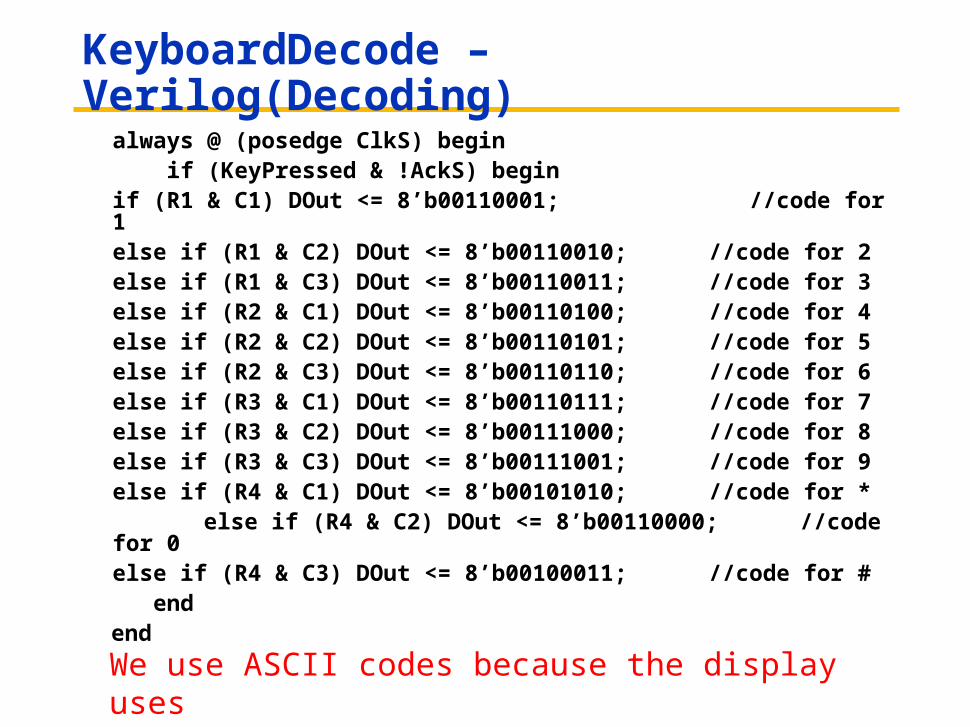
KeyboardDecode – Verilog(Decoding)
always @ (posedge ClkS) begin if (KeyPressed & !AckS) begin
if (R1 & C1) DOut <= 8’b00110001; //code for 1else if (R1 & C2) DOut <= 8’b00110010; //code for 2else if (R1 & C3) DOut <= 8’b00110011; //code for 3else if (R2 & C1) DOut <= 8’b00110100; //code for 4else if (R2 & C2) DOut <= 8’b00110101; //code for 5else if (R2 & C3) DOut <= 8’b00110110; //code for 6else if (R3 & C1) DOut <= 8’b00110111; //code for 7else if (R3 & C2) DOut <= 8’b00111000; //code for 8else if (R3 & C3) DOut <= 8’b00111001; //code for 9else if (R4 & C1) DOut <= 8’b00101010; //code for *
else if (R4 & C2) DOut <= 8’b00110000; //code for 0else if (R4 & C3) DOut <= 8’b00100011; //code for #
end end
We use ASCII codes because the display uses
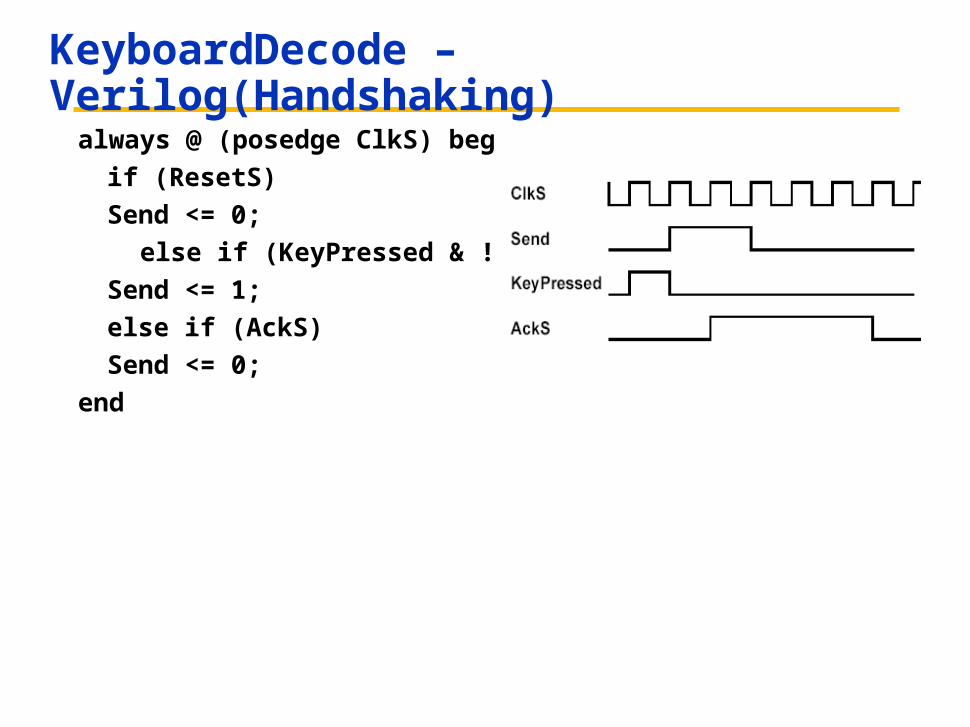
KeyboardDecode – Verilog(Handshaking)
always @ (posedge ClkS) begin
if (ResetS)
Send <= 0;
else if (KeyPressed & !AckS)
Send <= 1;
else if (AckS)
Send <= 0;
end
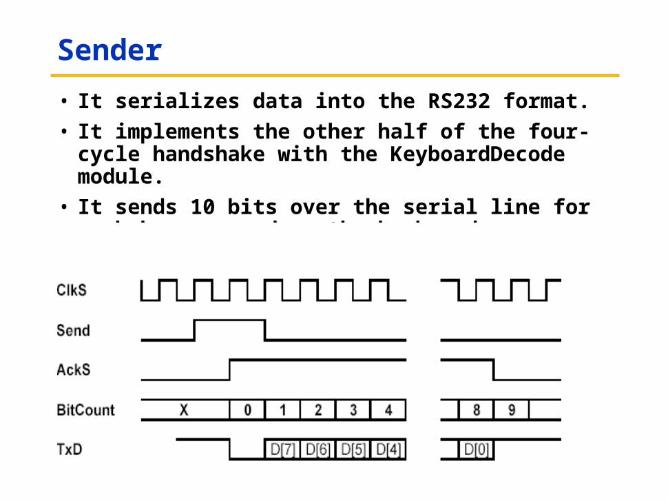
Sender
• It serializes data into the RS232 format.
• It implements the other half of the four-cycle handshake with the KeyboardDecode module.
• It sends 10 bits over the serial line for each key pressed on the keyboard.
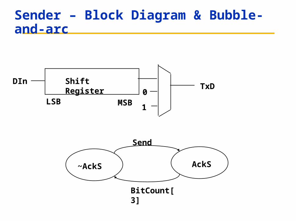
Sender – Block Diagram & Bubble-and-arc
Shift RegisterDIn
LSB MSB
TxD
AckS
0
1
~AckS
Send
BitCount[3]
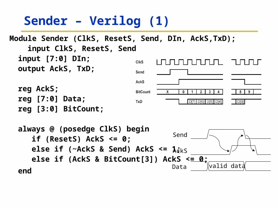
Sender – Verilog (1)Module Sender (ClkS, ResetS, Send, DIn, AckS,TxD); input ClkS, ResetS, Send;
input [7:0] DIn;output AckS, TxD;
reg AckS;reg [7:0] Data;reg [3:0] BitCount;
always @ (posedge ClkS) begin if (ResetS) AckS <= 0; else if (~AckS & Send) AckS <= 1; else if (AckS & BitCount[3]) AckS <= 0;
endvalid dataData
AckS
Send
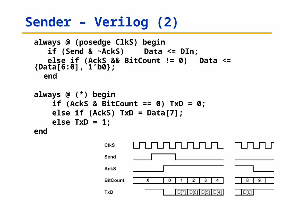
Sender – Verilog (2)
always @ (posedge ClkS) begin if (Send & ~AckS) Data <= DIn; else if (AckS && BitCount != 0) Data <= {Data[6:0], 1’b0};
end
always @ (*) begin if (AckS & BitCount == 0) TxD = 0; else if (AckS) TxD = Data[7]; else TxD = 1;end
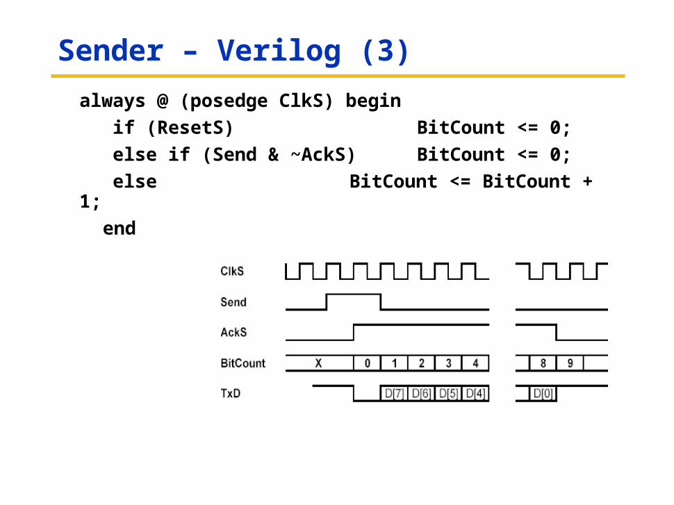
Sender – Verilog (3)
always @ (posedge ClkS) begin
if (ResetS) BitCount <= 0;
else if (Send & ~AckS) BitCount <= 0;
else BitCount <= BitCount + 1;
end
Announcements
• Midterm on Tuesday 11/09– No notes
• Midterm Review on Monday 11/08– 5:30 – 8:00 in 125 Cory
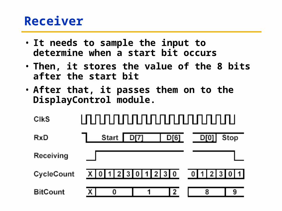
Receiver
• It needs to sample the input to determine when a start bit occurs
• Then, it stores the value of the 8 bits after the start bit
• After that, it passes them on to the DisplayControl module.
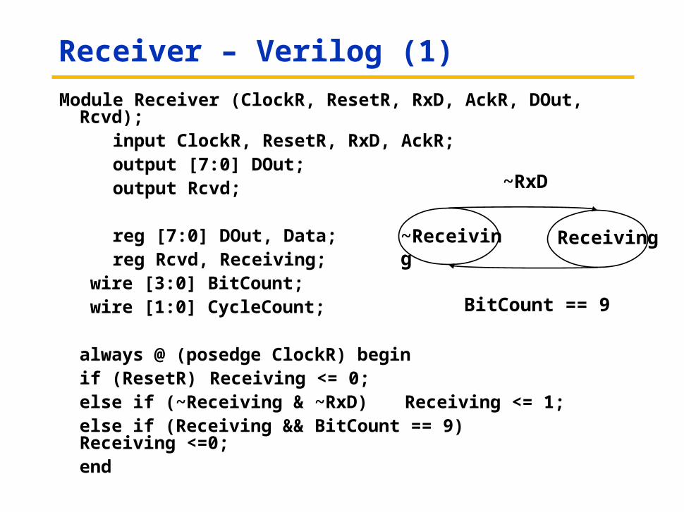
Receiver – Verilog (1)
Module Receiver (ClockR, ResetR, RxD, AckR, DOut, Rcvd); input ClockR, ResetR, RxD, AckR; output [7:0] DOut; output Rcvd;
reg [7:0] DOut, Data; reg Rcvd, Receiving;
wire [3:0] BitCount; wire [1:0] CycleCount;
always @ (posedge ClockR) beginif (ResetR) Receiving <= 0;else if (~Receiving & ~RxD) Receiving <= 1;else if (Receiving && BitCount == 9) Receiving <=0;
end
Receiving~Receiving
~RxD
BitCount == 9
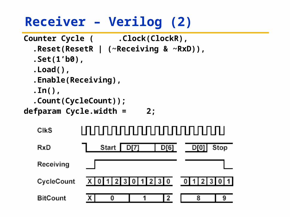
Receiver – Verilog (2)Counter Cycle ( .Clock(ClockR),
.Reset(ResetR | (~Receiving & ~RxD)),
.Set(1’b0),
.Load(),
.Enable(Receiving),
.In(),
.Count(CycleCount));defparam Cycle.width = 2;
Receiver – Verilog (3)
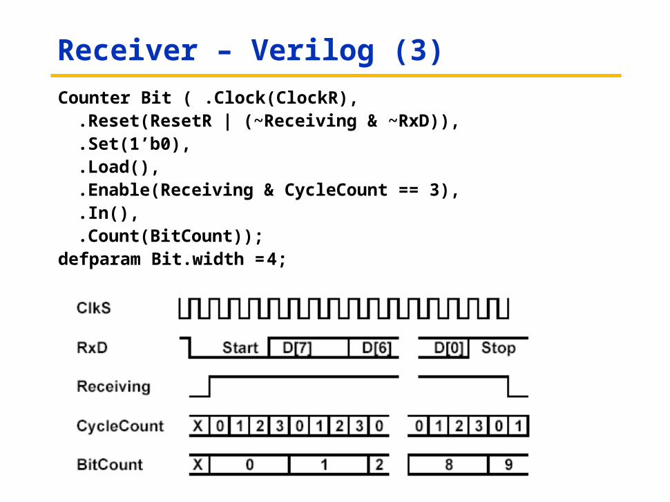
Counter Bit ( .Clock(ClockR), .Reset(ResetR | (~Receiving & ~RxD)),.Set(1’b0), .Load(), .Enable(Receiving & CycleCount == 3), .In(), .Count(BitCount));
defparam Bit.width = 4;
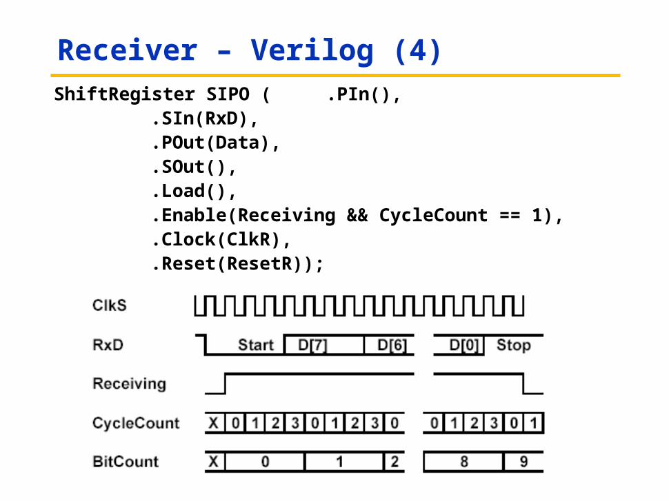
Receiver – Verilog (4)ShiftRegister SIPO ( .PIn(),
.SIn(RxD), .POut(Data), .SOut(), .Load(), .Enable(Receiving && CycleCount == 1), .Clock(ClkR), .Reset(ResetR));
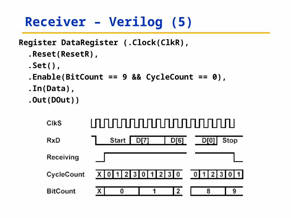
Receiver – Verilog (5)
Register DataRegister (.Clock(ClkR),
.Reset(ResetR),
.Set(),
.Enable(BitCount == 9 && CycleCount == 0),
.In(Data),
.Out(DOut))
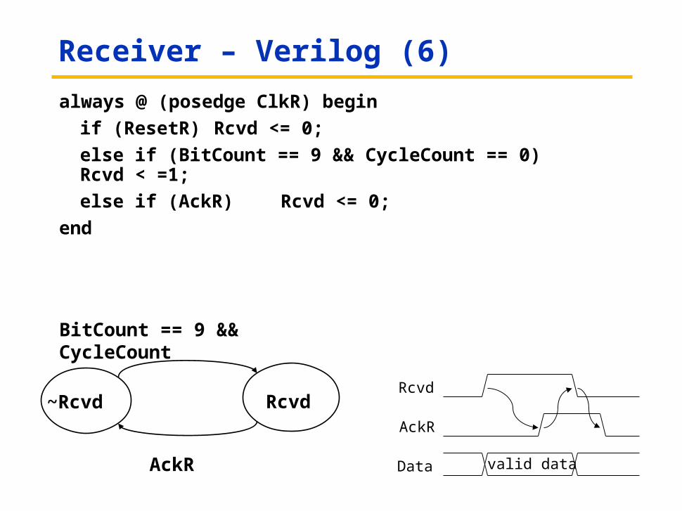
Receiver – Verilog (6)
always @ (posedge ClkR) begin
if (ResetR) Rcvd <= 0;
else if (BitCount == 9 && CycleCount == 0) Rcvd < =1;
else if (AckR) Rcvd <= 0;
end
valid dataData
AckR
RcvdRcvd~Rcvd
BitCount == 9 && CycleCount
AckR
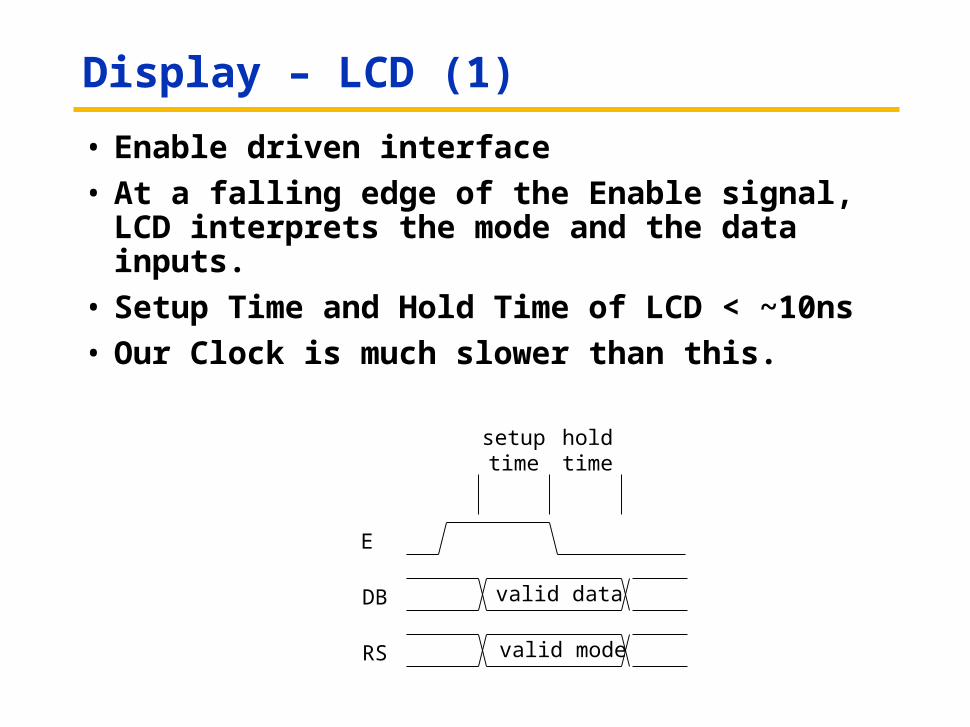
Display – LCD (1)
• Enable driven interface
• At a falling edge of the Enable signal, LCD interprets the mode and the data inputs.
• Setup Time and Hold Time of LCD < ~10ns
• Our Clock is much slower than this.
valid dataDB
E
valid modeRS
setuptime
holdtime
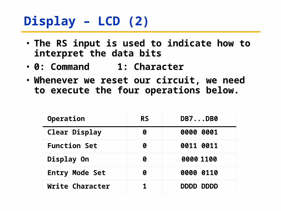
Display – LCD (2)
• The RS input is used to indicate how to interpret the data bits
• 0: Command 1: Character
• Whenever we reset our circuit, we need to execute the four operations below.
Operation RS DB7...DB0
Clear Display 0 0000 0001
Function Set 0 0011 0011
Display On 0 0000 1100
Entry Mode Set 0 0000 0110
Write Character 1 DDDD DDDD
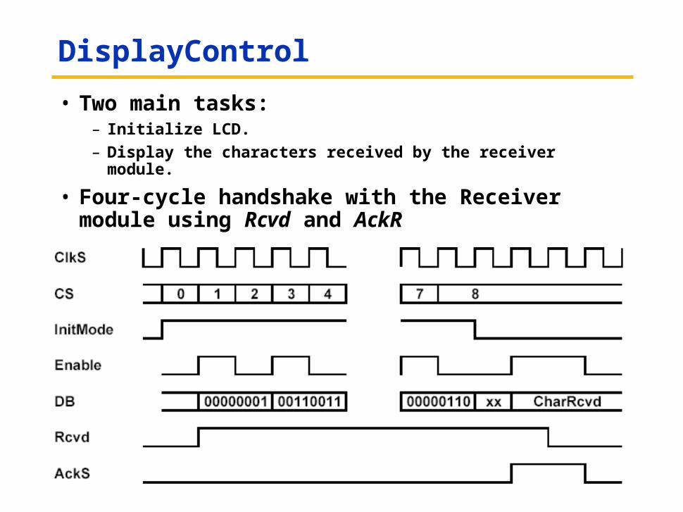
DisplayControl
• Two main tasks:– Initialize LCD.
– Display the characters received by the receiver module.
• Four-cycle handshake with the Receiver module using Rcvd and AckR
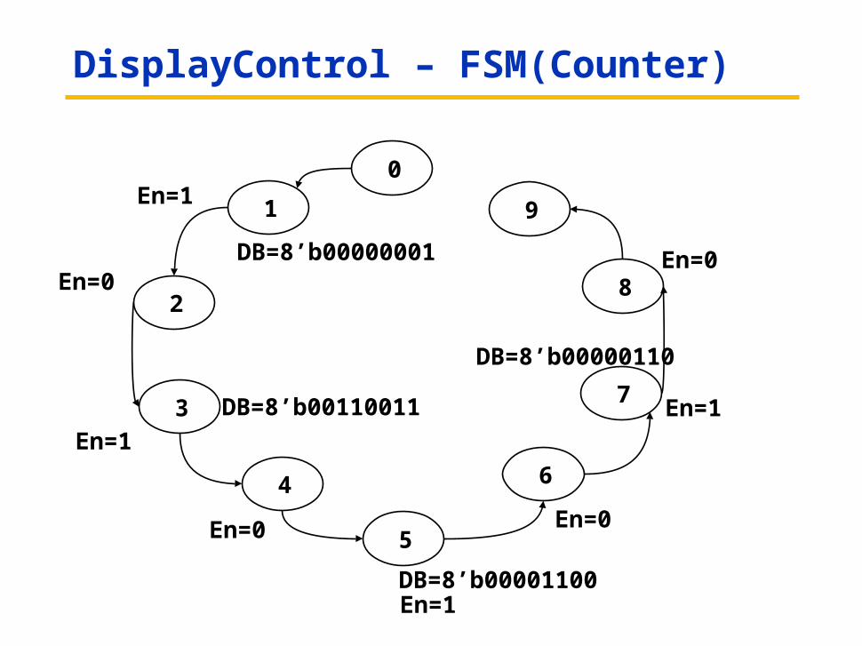
DisplayControl – FSM(Counter)
1
2
3
4
5
6
7
8
9
0
DB=8’b00000001
DB=8’b00110011
DB=8’b00001100
DB=8’b00000110
En=1
En=1
En=1
En=1
En=0
En=0 En=0
En=0
DisplayControl – Verilog (1)
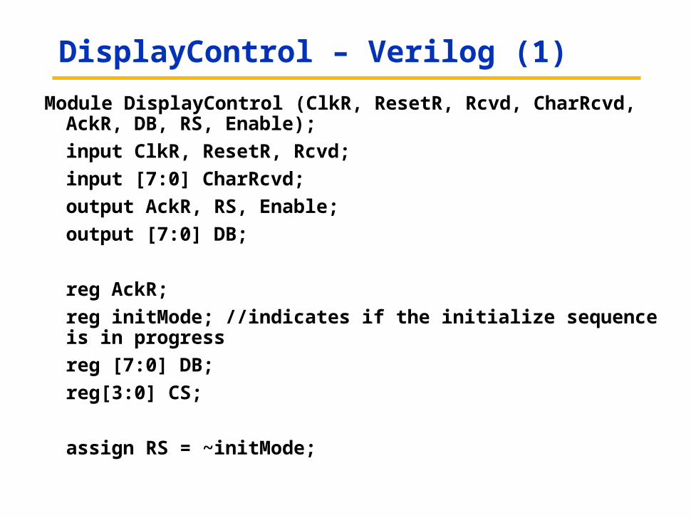
Module DisplayControl (ClkR, ResetR, Rcvd, CharRcvd, AckR, DB, RS, Enable);
input ClkR, ResetR, Rcvd;
input [7:0] CharRcvd;
output AckR, RS, Enable;
output [7:0] DB;
reg AckR;
reg initMode; //indicates if the initialize sequence is in progress
reg [7:0] DB;
reg[3:0] CS;
assign RS = ~initMode;
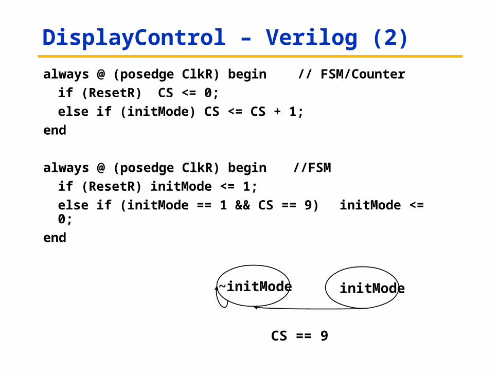
DisplayControl – Verilog (2)
always @ (posedge ClkR) begin // FSM/Counter
if (ResetR) CS <= 0;
else if (initMode) CS <= CS + 1;
end
always @ (posedge ClkR) begin //FSM
if (ResetR) initMode <= 1;
else if (initMode == 1 && CS == 9) initMode <= 0;
end
initMode~initMode
CS == 9
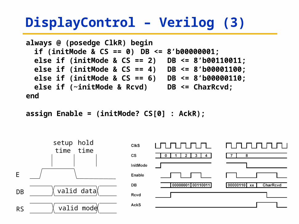
DisplayControl – Verilog (3)
always @ (posedge ClkR) beginif (initMode & CS == 0) DB <= 8’b00000001; else if (initMode & CS == 2) DB <= 8’b00110011; else if (initMode & CS == 4) DB <= 8’b00001100; else if (initMode & CS == 6) DB <= 8’b00000110; else if (~initMode & Rcvd) DB <= CharRcvd;
end
assign Enable = (initMode? CS[0] : AckR);
valid dataDB
E
valid modeRS
setuptime
holdtime
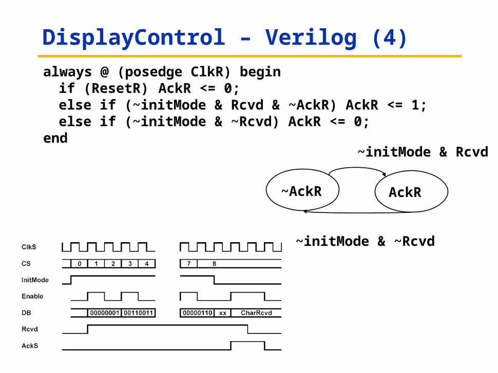
DisplayControl – Verilog (4)
always @ (posedge ClkR) beginif (ResetR) AckR <= 0;else if (~initMode & Rcvd & ~AckR) AckR <= 1;else if (~initMode & ~Rcvd) AckR <= 0;
end
AckR~AckR
~initMode & ~Rcvd
~initMode & Rcvd
Summary
• What is the point of this case study– to show how to breakdown a larger problem into components
– to show how to define the interfaces between components
• There are many ways to accomplish this, the design presented here is merely one of these.
• Most of the design choices were made so as to make the implementation easy to understand.