eecs 151/251a asic lab 3: logic synthesis overvieeecs151/sp18/files/lab3_asic.pdf · eecs 151/251a...
TRANSCRIPT
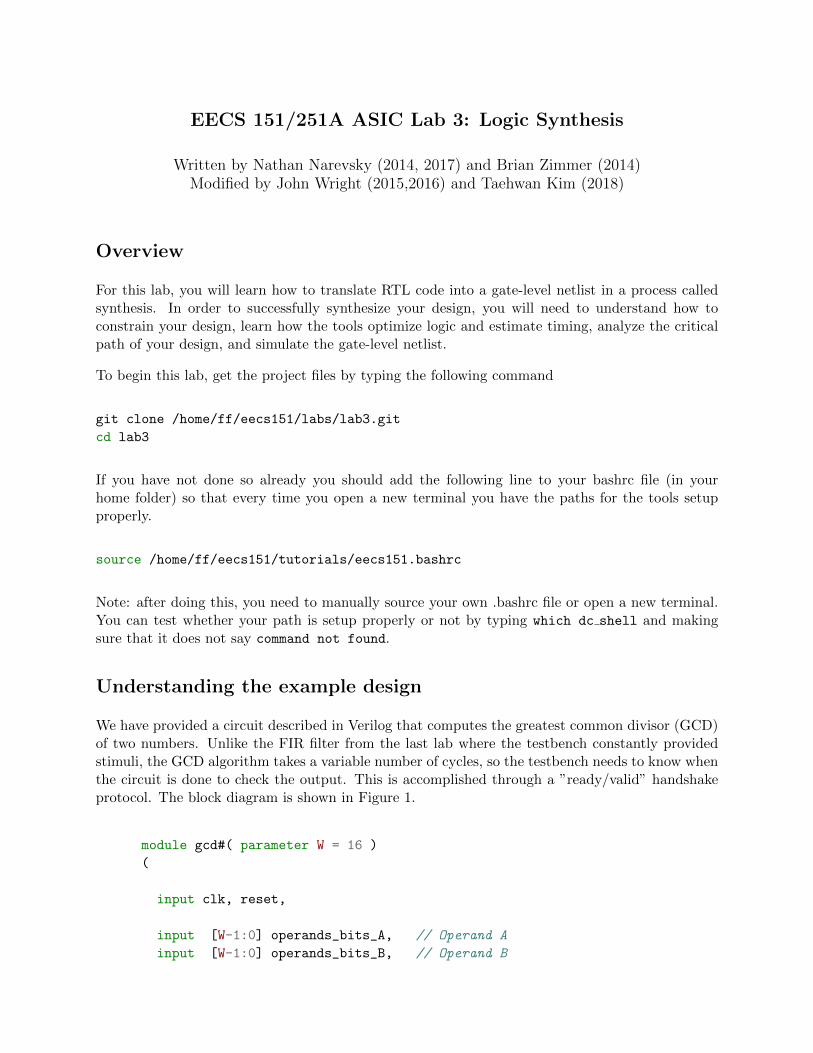
EECS 151/251A ASIC Lab 3: Logic Synthesis
Written by Nathan Narevsky (2014, 2017) and Brian Zimmer (2014)
Modified by John Wright (2015,2016) and Taehwan Kim (2018)
Overview
For this lab, you will learn how to translate RTL code into a gate-level netlist in a process calledsynthesis. In order to successfully synthesize your design, you will need to understand how toconstrain your design, learn how the tools optimize logic and estimate timing, analyze the criticalpath of your design, and simulate the gate-level netlist.
To begin this lab, get the project files by typing the following command
git clone /home/ff/eecs151/labs/lab3.git
cd lab3
If you have not done so already you should add the following line to your bashrc file (in yourhome folder) so that every time you open a new terminal you have the paths for the tools setupproperly.
source /home/ff/eecs151/tutorials/eecs151.bashrc
Note: after doing this, you need to manually source your own .bashrc file or open a new terminal.You can test whether your path is setup properly or not by typing which dc shell and makingsure that it does not say command not found.
Understanding the example design
We have provided a circuit described in Verilog that computes the greatest common divisor (GCD)of two numbers. Unlike the FIR filter from the last lab where the testbench constantly providedstimuli, the GCD algorithm takes a variable number of cycles, so the testbench needs to know whenthe circuit is done to check the output. This is accomplished through a ”ready/valid” handshakeprotocol. The block diagram is shown in Figure 1.
module gcd#( parameter W = 16 )
(
input clk, reset,
input [W-1:0] operands_bits_A, // Operand A
input [W-1:0] operands_bits_B, // Operand B

EECS 151/251A ASIC Lab 3: Logic Synthesis 2
input operands_val, // Are operands valid?
output operands_rdy, // ready to take operands
output [W-1:0] result_bits_data, // GCD
output result_val, // Is the result valid?
input result_rdy // ready to take the result
);
gcdGCDUnit
gcdTestHarness
operands_bits_A
operands_bits_B
operands_val
operands_rdy
result_bits_data
result_rdy
result_val clk
reset
Figure 1: Block diagram for GCD Test Harness
On the operands boundary, nothing will happen until GCD is ready to receive data (operands rdy).When this happens, the testbench will place data on the operands (operands bits A and operands bits B),but GCD will not start until the testbench declares that these operands are valid (operands val).Then GCD will start.
The testbench needs to know that GCD is not done. This will be true as long as result val is 0(the results are not valid). Also, even if GCD is finished, it will hold the result until the testbench isprepared to receive the data (result rdy). The testbench will check the data when GCD declaresthe results are valid by setting result val to 1.
The main contract is that if the interface declares it is ready, and the other side declares valid, theinformation must be transfered.
Open src/gcd.v. This is the top-level of GCD and just instantiates gcd control and gcd datapath.Separating files into control and datapath is generally a good idea. Open src/gcd datapath.v.This file stores the operands, and contains the logic necessary to implement the algorithm (subtrac-
EECS 151/251A ASIC Lab 3: Logic Synthesis 3
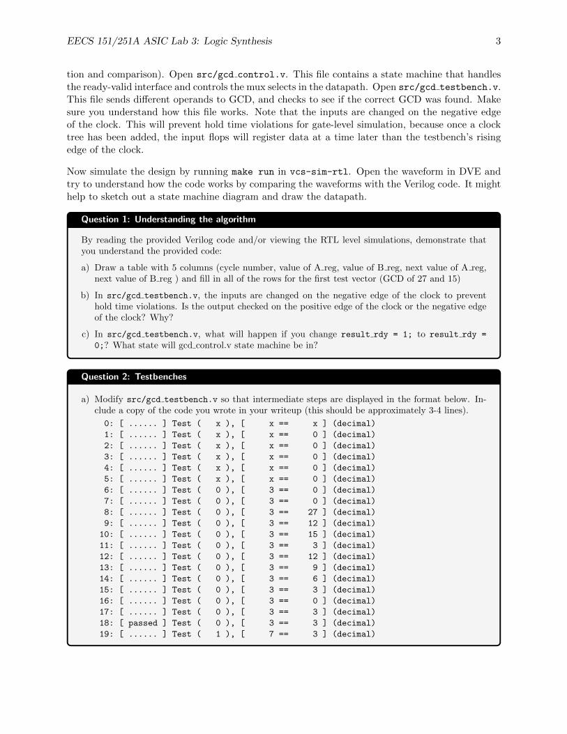
tion and comparison). Open src/gcd control.v. This file contains a state machine that handlesthe ready-valid interface and controls the mux selects in the datapath. Open src/gcd testbench.v.This file sends di↵erent operands to GCD, and checks to see if the correct GCD was found. Makesure you understand how this file works. Note that the inputs are changed on the negative edgeof the clock. This will prevent hold time violations for gate-level simulation, because once a clocktree has been added, the input flops will register data at a time later than the testbench’s risingedge of the clock.
Now simulate the design by running make run in vcs-sim-rtl. Open the waveform in DVE andtry to understand how the code works by comparing the waveforms with the Verilog code. It mighthelp to sketch out a state machine diagram and draw the datapath.
Question 1: Understanding the algorithm
By reading the provided Verilog code and/or viewing the RTL level simulations, demonstrate thatyou understand the provided code:
a) Draw a table with 5 columns (cycle number, value of A reg, value of B reg, next value of A reg,next value of B reg ) and fill in all of the rows for the first test vector (GCD of 27 and 15)
b) In src/gcd testbench.v, the inputs are changed on the negative edge of the clock to preventhold time violations. Is the output checked on the positive edge of the clock or the negative edgeof the clock? Why?
c) In src/gcd testbench.v, what will happen if you change result rdy = 1; to result rdy =0;? What state will gcd control.v state machine be in?
Question 2: Testbenches
a) Modify src/gcd testbench.v so that intermediate steps are displayed in the format below. In-clude a copy of the code you wrote in your writeup (this should be approximately 3-4 lines).
0: [ ...... ] Test ( x ), [ x == x ] (decimal)1: [ ...... ] Test ( x ), [ x == 0 ] (decimal)2: [ ...... ] Test ( x ), [ x == 0 ] (decimal)3: [ ...... ] Test ( x ), [ x == 0 ] (decimal)4: [ ...... ] Test ( x ), [ x == 0 ] (decimal)5: [ ...... ] Test ( x ), [ x == 0 ] (decimal)6: [ ...... ] Test ( 0 ), [ 3 == 0 ] (decimal)7: [ ...... ] Test ( 0 ), [ 3 == 0 ] (decimal)8: [ ...... ] Test ( 0 ), [ 3 == 27 ] (decimal)9: [ ...... ] Test ( 0 ), [ 3 == 12 ] (decimal)10: [ ...... ] Test ( 0 ), [ 3 == 15 ] (decimal)11: [ ...... ] Test ( 0 ), [ 3 == 3 ] (decimal)12: [ ...... ] Test ( 0 ), [ 3 == 12 ] (decimal)13: [ ...... ] Test ( 0 ), [ 3 == 9 ] (decimal)14: [ ...... ] Test ( 0 ), [ 3 == 6 ] (decimal)15: [ ...... ] Test ( 0 ), [ 3 == 3 ] (decimal)16: [ ...... ] Test ( 0 ), [ 3 == 0 ] (decimal)17: [ ...... ] Test ( 0 ), [ 3 == 3 ] (decimal)18: [ passed ] Test ( 0 ), [ 3 == 3 ] (decimal)19: [ ...... ] Test ( 1 ), [ 7 == 3 ] (decimal)
EECS 151/251A ASIC Lab 3: Logic Synthesis 4
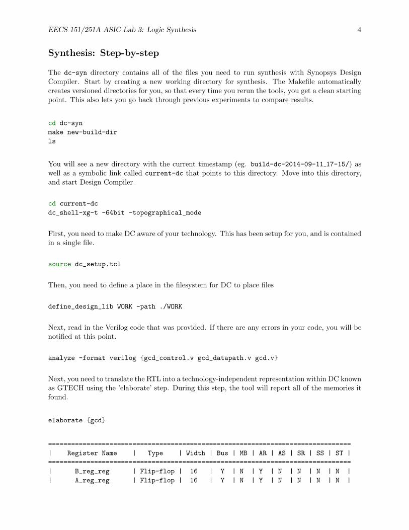
Synthesis: Step-by-step
The dc-syn directory contains all of the files you need to run synthesis with Synopsys DesignCompiler. Start by creating a new working directory for synthesis. The Makefile automaticallycreates versioned directories for you, so that every time you rerun the tools, you get a clean startingpoint. This also lets you go back through previous experiments to compare results.
cd dc-syn
make new-build-dir
ls
You will see a new directory with the current timestamp (eg. build-dc-2014-09-11 17-15/) aswell as a symbolic link called current-dc that points to this directory. Move into this directory,and start Design Compiler.
cd current-dc
dc_shell-xg-t -64bit -topographical_mode
First, you need to make DC aware of your technology. This has been setup for you, and is containedin a single file.
source dc_setup.tcl
Then, you need to define a place in the filesystem for DC to place files
define_design_lib WORK -path ./WORK
Next, read in the Verilog code that was provided. If there are any errors in your code, you will benotified at this point.
analyze -format verilog {gcd_control.v gcd_datapath.v gcd.v}
Next, you need to translate the RTL into a technology-independent representation within DC knownas GTECH using the ’elaborate’ step. During this step, the tool will report all of the memories itfound.
elaborate {gcd}
===============================================================================
| Register Name | Type | Width | Bus | MB | AR | AS | SR | SS | ST |
===============================================================================
| B_reg_reg | Flip-flop | 16 | Y | N | Y | N | N | N | N |
| A_reg_reg | Flip-flop | 16 | Y | N | Y | N | N | N | N |

EECS 151/251A ASIC Lab 3: Logic Synthesis 5
===============================================================================
===============================================================================
| Register Name | Type | Width | Bus | MB | AR | AS | SR | SS | ST |
===============================================================================
| state_reg | Flip-flop | 2 | Y | N | N | N | N | N | N |
===============================================================================
As expected, A/B are registers, and the state machine needs two flip-flops to hold the current state.
At this point, synthesis needs to know about the constraints of your design (eg. how fast the clockis). The units for these constraints are ns for timing and pF for capacitance.
create_clock clk -name clk1 -period 0.7
set_clock_uncertainty 0.05 [get_clocks clk1]
set_driving_cell -lib_cell INVX1_RVT [all_inputs]
set max_cap [expr [load_of saed32rvt_tt1p05v25c/AND2X1_RVT/A1] * 5]
set_load $max_cap [all_outputs]
The first line here creates a clock named clk1 with a period of 0.7ns. It is connected to the portclk at the input of the verilog module. The next line creates clock uncertainty, which is meantto model variations in the input clock signal, as well as negative e↵ects coming from the clocknetwork. Design compiler does not create a clock tree, so these contraints are used when checkingtiming with an ideal clock network. The set driving cell command tells the tools what cells aredriving all of the inputs, and the cell specified in this case is an inverter from the library. The setmax cap instruction creates a variable that is equal to 5 times the loading of a two input AND gate.The set load command sets the loading for this block’s outputs to be equal to the variable thatthe previous command created.
Before you continue with synthesis, look at what the tool knows about your design so far.
start_gui
In Hier.1 panel, right click on gcd — Schematic View. Then double click on the control block todive into this part of the hierarchy.
Notice that there are no actual standard cells yet. DC understands our design, but has yet to mapit to a technology or apply the constraints. The next command does almost all of synthesis in asingle command.
compile_ultra -gate_clock -no_autoungroup
The compile ultra command will report how the design is being optimized. You should see DesignCompiler performing technology mapping, delay optimization, and area reduction. The fragmentfrom the compile ultra shows the worst negative slack which indicates how much room there is

EECS 151/251A ASIC Lab 3: Logic Synthesis 6
between the critical path in your design and the clock constraint. Larger negative slack valuesare worse since this means that your design is missing the desired clock frequency by a greatamount. Total negative slack is the sum of all negative slack across all endpoints in the design.The gate clock flag enables clock gating optimization, which automatically inserts clock gates toreduce dynamic power by not clocking registers that do not need to be updated every clock cycle.The no autoungroup flag tells the tool to not automatically ungroup the design. This means thatthe hierarchy is preserved, which is very useful for designs when you need to speficy constraints ona specific cell in the hierarchy. If the tool removes the hierarchy, finding the same cell again can bevery di�cult, if not impossible, so we will typically use this flag.
Beginning Timing Optimization-----------------------------
TOTALELAPSED WORST NEG SETUP DESIGN LEAKAGETIME AREA SLACK COST RULE COST ENDPOINT POWER
--------- --------- --------- --------- --------- ------------------------- ---------0:00:14 873.0 0.00 0.0 0.0 83824648.00000:00:14 873.0 0.00 0.0 0.0 83824648.00000:00:14 873.0 0.00 0.0 0.0 83824648.00000:00:14 873.0 0.00 0.0 0.0 83824648.00000:00:14 873.0 0.00 0.0 0.0 83824648.0000
Now look at the schematic again. Now you can see that the design only consists of actual standardcells now.
At this point, it is a good idea to check the design.
check_design
Warning: In design 'gcd_datapath_W16', port 'A_mux_sel[0]' is not connected to any nets. (LINT-28)Warning: In design 'gcd_control', port 'A_mux_sel[0]' is not connected to any nets. (LINT-28)Warning: In design 'gcd', a pin on submodule 'GCDdpath0' is connected to logic 1 or logic 0. (LINT-32)
Pin 'A_mux_sel[0]' is connected to logic 0.Warning: In design 'gcd_datapath_W16', a pin on submodule 'clk_gate_B_reg_reg' is connected to logic 1 or logic 0. (LINT-32)
Pin 'TE' is connected to logic 0.Warning: In design 'gcd_datapath_W16', a pin on submodule 'clk_gate_A_reg_reg' is connected to logic 1 or logic 0. (LINT-32)
Pin 'TE' is connected to logic 0.
The ’TE’ warning is not a problem (we don’t have scan in this design, so the scan enable pins ishardwired to 0). However, the other three warnings are interesting. Look at the RTL and figureout why we see this error.
Question 3: Synthesis optimization
a) Why is A mux sel[0] not connected to any nets? Why is this ok? Is there some other pin that hasthe same functionality?

EECS 151/251A ASIC Lab 3: Logic Synthesis 7
With the -no autoungroup flag, DC never changes the ports on your hierarchical modules. If youwant to clear this warning, you can let DC ungroup your hierarchy.
compile_ultra -gate_clock
check_design
Now, generate a quality-of-result (QOR) summary)
report_qor
From this report, you know the maximum speed of your design (Critical Path Clk Period - CriticalPath Slack).
Timing Path Group 'clk1'
-----------------------------------
Levels of Logic: 12.00
Critical Path Length: 0.57
Critical Path Slack: 0.04
Critical Path Clk Period: 0.70
Total Negative Slack: 0.00
No. of Violating Paths: 0.00
Worst Hold Violation: 0.00
Total Hold Violation: 0.00
No. of Hold Violations: 0.00
-----------------------------------
So what path is setting the maximum frequency?
report_timing -capacitance -transition_time -input_pins -significant_digits 3
The following timing report explains the critical path in the design. The path starts when the clockarrives at A reg reg[8], and the value needs to arrive at the D input of the flip-flop A reg reg[11]within the clock period minus the clock uncertainty minus the setup time of the flop.
The fanout column tells you how many other pins the current output drives, and the capacitancecolumn tells you how much capacitance the tool calculated for that net. The transition time is therise or fall time of the node (notice the last column tells you whether the rise or fall transition isthe transition on the path). The Incr column shows the incremental delay through each logic gate.If any section shows ”VIOLATED“ instead of ”MET“, you have a timing violation (which will alsoshow as negative slack in the QOR summary).
Operating Conditions: tt1p05v25c Library: saed32rvt_tt1p05v25cWire Load Model Mode: Inactive.
Startpoint: GCDdpath0/A_reg_reg_1_
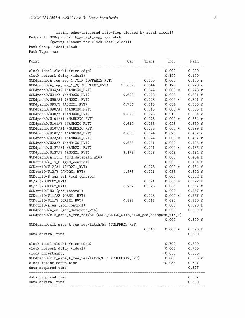
EECS 151/251A ASIC Lab 3: Logic Synthesis 8
(rising edge-triggered flip-flop clocked by ideal_clock1)Endpoint: GCDdpath0/clk_gate_A_reg_reg/latch
(gating element for clock ideal_clock1)Path Group: ideal_clock1Path Type: max
Point Cap Trans Incr Path------------------------------------------------------------------------------------clock ideal_clock1 (rise edge) 0.000 0.000clock network delay (ideal) 0.150 0.150GCDdpath0/A_reg_reg_1_/CLK (DFFARX2_RVT) 0.000 0.000 0.150 rGCDdpath0/A_reg_reg_1_/Q (DFFARX2_RVT) 11.002 0.044 0.128 0.278 rGCDdpath0/U94/A2 (NAND2X0_RVT) 0.044 0.000 * 0.278 rGCDdpath0/U94/Y (NAND2X0_RVT) 0.698 0.028 0.023 0.301 fGCDdpath0/U95/A4 (AO22X1_RVT) 0.028 0.000 * 0.301 fGCDdpath0/U95/Y (AO22X1_RVT) 0.706 0.015 0.034 0.335 fGCDdpath0/U98/A1 (NAND3X0_RVT) 0.015 0.000 * 0.335 fGCDdpath0/U98/Y (NAND3X0_RVT) 0.640 0.025 0.018 0.354 rGCDdpath0/U101/A1 (NAND3X0_RVT) 0.025 0.000 * 0.354 rGCDdpath0/U101/Y (NAND3X0_RVT) 0.619 0.033 0.026 0.379 fGCDdpath0/U107/A1 (NAND2X0_RVT) 0.033 0.000 * 0.379 fGCDdpath0/U107/Y (NAND2X0_RVT) 0.603 0.024 0.028 0.407 rGCDdpath0/U23/A1 (NAND4X0_RVT) 0.024 0.000 * 0.407 rGCDdpath0/U23/Y (NAND4X0_RVT) 0.655 0.041 0.029 0.436 fGCDdpath0/U127/A1 (AND2X1_RVT) 0.041 0.000 * 0.436 fGCDdpath0/U127/Y (AND2X1_RVT) 3.173 0.028 0.048 0.484 fGCDdpath0/A_lt_B (gcd_datapath_W16) 0.000 0.484 fGCDctrl0/A_lt_B (gcd_control) 0.000 0.484 fGCDctrl0/U12/A1 (AND2X1_RVT) 0.028 0.000 * 0.484 fGCDctrl0/U12/Y (AND2X1_RVT) 1.875 0.021 0.038 0.522 fGCDctrl0/B_mux_sel (gcd_control) 0.000 0.522 fU5/A (NBUFFX2_RVT) 0.021 0.000 * 0.522 fU5/Y (NBUFFX2_RVT) 5.287 0.023 0.036 0.557 fGCDctrl0/IN0 (gcd_control) 0.000 0.557 fGCDctrl0/U11/A3 (OR3X1_RVT) 0.023 0.000 * 0.557 fGCDctrl0/U11/Y (OR3X1_RVT) 0.537 0.016 0.032 0.590 fGCDctrl0/A_en (gcd_control) 0.000 0.590 fGCDdpath0/A_en (gcd_datapath_W16) 0.000 0.590 fGCDdpath0/clk_gate_A_reg_reg/EN (SNPS_CLOCK_GATE_HIGH_gcd_datapath_W16_1)
0.000 0.590 fGCDdpath0/clk_gate_A_reg_reg/latch/EN (CGLPPRX2_RVT)
0.016 0.000 * 0.590 fdata arrival time 0.590
clock ideal_clock1 (rise edge) 0.700 0.700clock network delay (ideal) 0.000 0.700clock uncertainty -0.035 0.665GCDdpath0/clk_gate_A_reg_reg/latch/CLK (CGLPPRX2_RVT) 0.000 0.665 rclock gating setup time -0.058 0.607data required time 0.607------------------------------------------------------------------------------------data required time 0.607data arrival time -0.590------------------------------------------------------------------------------------
EECS 151/251A ASIC Lab 3: Logic Synthesis 9
slack (MET) 0.017
These values are calculated by the .db files included by the source dc setup.tcl command. Thedb file is a binary file that describes the delay through various gates depending on the input slopeand the output capacitance. The .db file is generated from a textual .lib file, which is created byrunning transistor-level simulations of each standard cell in a process called “cell characterization.”
In a separate terminal, open the .lib file that generated the .db file.
vim /home/ff/eecs151/stdcells/synopsys-32nm/vendor/
lib/stdcell_rvt/db_nldm/saed32rvt_tt1p05v25c.lib
Search for NAND2X0 RVT (line 78311). We would like to understand where the following line in thecritical path comes from:
Point Cap Trans Incr Path------------------------------------------------------------------------------------GCDdpath0/U94/A2 (NAND2X0_RVT) 0.044 0.000 * 0.278 rGCDdpath0/U94/Y (NAND2X0_RVT) 0.698 0.028 0.023 0.301 f
Inside the lib file, we search for the correct cell (NAND2X0 RVT), the output pin (Y), the relatedinput pin (A2) and we find a 2d table where each row corresponds to di↵erent input net transitions(index 1) and each column corresponds to di↵erent output net capacitances (index 2).
cell (NAND2X0_RVT)...pin (Y)...timing () {related_pin : "A2";
cell_fall ("del_1_7_7") {index_1("0.016, 0.032, 0.064, 0.128, 0.256, 0.512, 1.024"); //input_net_transitionindex_2("0.1, 0.25, 0.5, 1, 2, 4, 8"); //total_output_net_capacitancevalues("0.0141691, 0.0158192, 0.0183277, 0.0231493, 0.0328029, 0.0521611, 0.0906369", \"0.0155022, 0.0175121, 0.0205658, 0.0262506, 0.0364229, 0.0557899, 0.0940605", \"0.0149406, 0.0176121, 0.0217530, 0.0289079, 0.0414177, 0.0628228, 0.1014903", \"0.0098307, 0.0133983, 0.0187084, 0.0284193, 0.0446767, 0.0712630, 0.1151648", \"-0.0046647, -0.0004140, 0.0064594, 0.0189513, 0.0407080, 0.0753612, 0.1308888", \"-0.0393372, -0.0338884, -0.0256511, -0.0098435, 0.0182941, 0.0633240, 0.1366469", \"-0.1132701, -0.1072634, -0.0973538, -0.0792401, -0.0452052, 0.0144727, 0.1094809");
In this case, the closest entry in the table would be index 1 between 1 and 2 (actual transitionof 0.044 between 0.032 and 0.064) and index 2 of between 2 and 3 (actual capacitance of 0.698between 0.5 and 1). This yields a delay value between 0.0205 and 0.0289, and the timing toolreports 0.023 as expected.
The same information will be generated in an .sdf file for gate-level simulation with annotateddelays. Reading these reports is very important, so make sure you understand all of these columns

EECS 151/251A ASIC Lab 3: Logic Synthesis 10
before you move on. There is a way to visualize this information within the GUI. Go to Timing —Timing Analysis Driver from the GUI menu items. This should pop up a window, simply click theOK button. You should now see a table of information, as shown in the picture below:
Figure 2: Timing Analysis Driver window
This is a representation of the previous timing report. Highlight the timing path with the smallestslack, and click on the Inspector button. Then click the Schematic button to load a new windowwith a schematic. Click on the Data Path window. You should see something similar to below:
Figure 3: Inspector window showing Data Path tab

EECS 151/251A ASIC Lab 3: Logic Synthesis 11
Under the Delay Profile tab it shows you which gates contribute to the delay. Expand thehierarchy and select the rows one at a time. Notice that when you click on a new row it highlightsa new point in the schematic window. You can walk through the entire critical path this way, andsee which gates are contributing what delay to that worst case path.
Figure 4: Delay profile tab with the output of the first register highlighted
Now let’s take a look at the power report:
report_power
Global Operating Voltage = 1.05Power-specific unit information :
Voltage Units = 1VCapacitance Units = 1.000000ffTime Units = 1nsDynamic Power Units = 1uW (derived from V,C,T units)Leakage Power Units = 1pW
Warning: Cannot report correlated power unless power prediction mode is set. (PWR-727)Power Breakdown---------------
Cell Driven Net Tot Dynamic CellInternal Switching Power (uW) Leakage
Cell Power (uW) Power (uW) (% Cell/Tot) Power (pW)--------------------------------------------------------------------------------Netlist Power 288.5137 88.6894 3.772e+02 (76%) 7.710e+07Estimated Clock Tree Power N/A N/A (N/A) N/A--------------------------------------------------------------------------------

EECS 151/251A ASIC Lab 3: Logic Synthesis 12
Internal Switching Leakage TotalPower Group Power Power Power Power ( % ) Attrs--------------------------------------------------------------------------------------------------io_pad 0.0000 0.0000 0.0000 0.0000 ( 0.00%)memory 0.0000 0.0000 0.0000 0.0000 ( 0.00%)black_box 0.0000 0.0000 0.0000 0.0000 ( 0.00%)clock_network 22.7097 26.8379 1.8522e+06 51.3998 ( 11.31%)register 189.3470 16.0004 3.5358e+07 240.7056 ( 52.98%)sequential 0.0000 0.0000 0.0000 0.0000 ( 0.00%)combinational 76.4570 45.8511 3.9891e+07 162.1994 ( 35.70%)--------------------------------------------------------------------------------------------------Total 288.5137 uW 88.6894 uW 7.7102e+07 pW 454.3048 uW1
The internal power comes from crowbar current during a transition, the switching power involvesswitching the output capacitance, and the cell leakage is the leakage of each cell. Without knowingthe switching activity of your design, the active power measurements will not be accurate, but theleakage will still be pretty accurate.
DC can also summarize the types and sizes of cells used in the design.
Another helpful reporting command is the following:
report_reference
****************************************
Report : reference
Design : gcd
Version: G-2012.06
Date : Fri Sep 12 15:06:49 2014
****************************************
Attributes:
b - black box (unknown)
bo - allows boundary optimization
d - dont_touch
mo - map_only
h - hierarchical
n - noncombinational
r - removable
s - synthetic operator
u - contains unmapped logic
Reference Library Unit Area Count Total Area Attributes
-----------------------------------------------------------------------------
INVX2_RVT saed32rvt_tt1p05v25c
1.524864 1 1.524864
NBUFFX2_RVT saed32rvt_tt1p05v25c

EECS 151/251A ASIC Lab 3: Logic Synthesis 13
2.033152 5 10.165761
gcd_control 50.320513 1 50.320513 h, n
gcd_datapath_W16 779.459651 1 779.459651 b, h, n
-----------------------------------------------------------------------------
Total 4 references 841.470788
1
The Total Area is the total area of all of the combined cells that are referenced in the design. Theunits of these are square micrometers, but keep in mind this is just the total area occupied by thestandard cells themselves. The place and route tool (which we will use in the next lab) is not goingto be able to pack everything together perfectly since a lot of the time you will be limited by theseother constraints. You can rerun this same command to expand into the submodules, by addingthe -hierarchy flag. This full command becomes:
report_reference -hierarchy
The output of this command is omitted from this lab writeup since it is very large, but pleaserun this command and briefly look through the cells that are referenced in the gcd control andgcd datapath submodules.
There are a lot of other command options that will not be discussed in detail, but can often bevery important. If you do not know what they are, there are a few commands that can be veryhandy for figuring out what to try. The following command will return the names of commandsthis tool supports that contain the word reference in them:
info comm *reference*
For example, one of the commands returned from this is the all rp references command. Whilewe have not gone over the topics to cover the details of this command, more information about it(and all other commands) can be found by typing:
man all_rp_references
If you are using the GUI you should see a documentation window pop up, which has a lot moreuseful information. Become familiar with these windows, as they will be crucial for the projectlater in the class.
Question 4: Exploring new commands
a) Find the net with the largest fanout. Report the net, the fanout, and the command(s) you usedto find it
b) Find the net with the largest capacitance. Is this the same as the net in the previous question?Again report the net, the capacitance and the command(s) you used to find it

EECS 151/251A ASIC Lab 3: Logic Synthesis 14
To exit from the dc shell you can either type exit or press Control-c a few times.
Automated Synthesis
While interactive control of synthesis is instructive, it would be too time consuming for real design.Instead, the Makefile and tcl scripts run all of the commands you just ran automatically.
cd lab3a_synthesis/dc-syn
make
This will run through all of the previous steps all in one shot, as well as setting up a suite of reportsand a few handy files for interactions with other tools. Go into the folder that you have createdwith the Makefile with the following command:
cd current-dc/
In here you should see a copy of the files from the previous folder, but the important folders topoint out are the results and reports folders. The results folder contains the outputs of DesignCompiler that will be used in other tools, and the reports folder contains more detailed versionsof the reports that we were looking at previously in the lab. Look through the reports folder andfamiliarize yourself with the di↵erent reports.
If you would now like to open the design to generate more reports or use the GUI, use the followingcommands.
cd current-dc
dc_shell-xg-t -64bit -topographical_mode
source dc_setup.tcl
read_ddc results/gcd.mapped.ddc
Question 5: Reporting Questions
a) Which report would you look at to find the total number of each di↵erent standard cell that thedesign contains?
b) Which report contains total cell counts contained within the design?
c) Which report contains information about how sub-blocks were actually implemented?
Post-Synthesis Simulation
From the root folder, type the following commands:
cd vcs-sim-gl-syn/
make run
EECS 151/251A ASIC Lab 3: Logic Synthesis 15
This will run a post-synthesis simulation, but does not use annotated delays from the sdf file. Thereason that we do this is because Design Compiler does not create a clock tree, so you can easilyhave a design that contains hold time violations in it that will be fixed during place and route. Theexample that we used in the previous lab had a fake clock tree added to it to demonstrate part ofthis, but we will discuss post place and route simulations in future labs. For now, simply ensurethat the design still simulates properly (passes the testbench).
Changing the Design
Question 6: Design changes
Now that you understand how to use the tools, change the GCD implementation from 16 bits to 128bits (this can be done in the gcd.v file). Push the new design through the tools, and determine itscritical path, cell area, and maximum operating frequency from the reports.
a) Did the design meet timing?
b) If not, rerun the tools with a new clock period that will work based on the extra time that youneed from the timing report. What is the clock period that you used and did that new choicework?
c) What is the critical path in the design?