eecs150 - digital design lecture 11 - static random access...
TRANSCRIPT
10/3/2013
1
1 Fall 2013 EECS150 - Lec11-sram Page
EECS150 - Digital Design
Lecture 11 - Static Random
Access Memory (SRAM)
Oct. 3, 2013
Prof. Ronald Fearing
Electrical Engineering and Computer Sciences
University of California, Berkeley
(slides courtesy of Prof. John Wawrzynek)
http://www-inst.eecs.berkeley.edu/~cs150
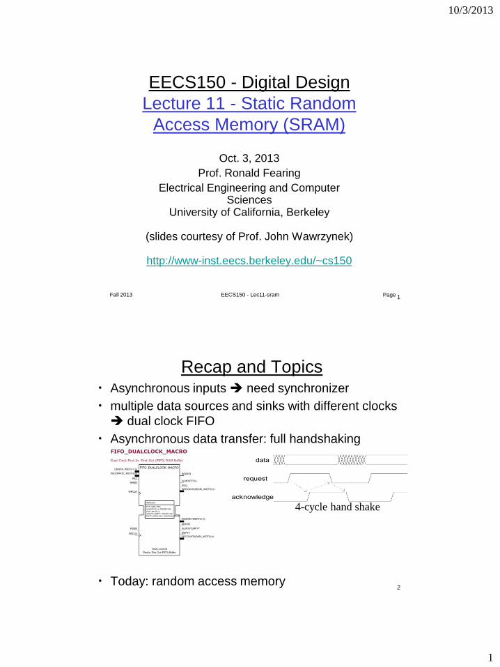
Recap and Topics • Asynchronous inputs need synchronizer
• multiple data sources and sinks with different clocks
dual clock FIFO
• Asynchronous data transfer: full handshaking
• Today: random access memory 2
4-cycle hand shake
10/3/2013
2
3 Fall 2013 EECS150 - Lec11-sram Page
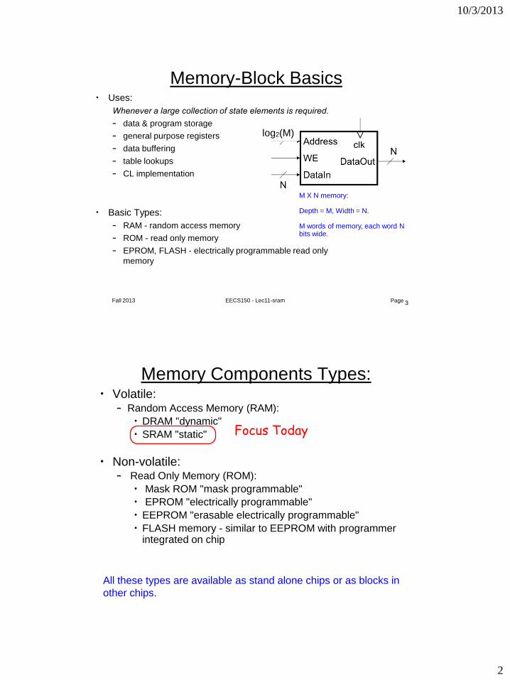
Memory-Block Basics • Uses:
Whenever a large collection of state elements is required.
– data & program storage
– general purpose registers
– data buffering
– table lookups
– CL implementation
• Basic Types:
– RAM - random access memory
– ROM - read only memory
– EPROM, FLASH - electrically programmable read only
memory
M X N memory: Depth = M, Width = N. M words of memory, each word N bits wide.
log2(M)
4 Fall 2013 EECS150 - Lec11-sram Page
Memory Components Types: • Volatile:
– Random Access Memory (RAM):
• DRAM "dynamic"
• SRAM "static"
• Non-volatile: – Read Only Memory (ROM):
• Mask ROM "mask programmable"
• EPROM "electrically programmable"
• EEPROM "erasable electrically programmable"
• FLASH memory - similar to EEPROM with programmer integrated on chip
4
Focus Today
All these types are available as stand alone chips or as blocks in
other chips.
10/3/2013
3
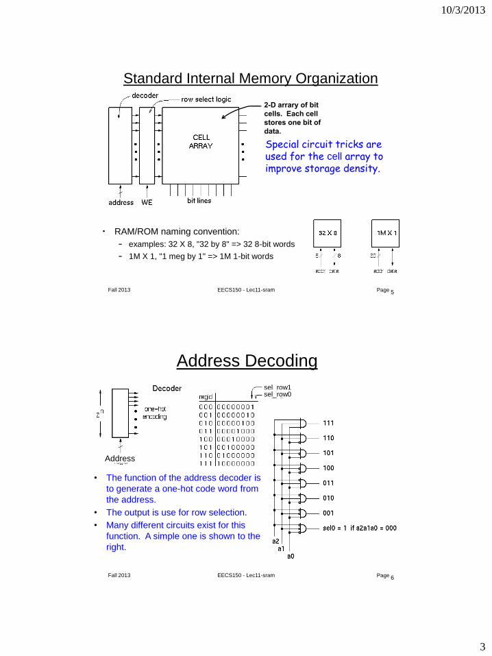
5 Fall 2013 EECS150 - Lec11-sram Page
Standard Internal Memory Organization
• RAM/ROM naming convention:
– examples: 32 X 8, "32 by 8" => 32 8-bit words
– 1M X 1, "1 meg by 1" => 1M 1-bit words
2-D arrary of bit
cells. Each cell
stores one bit of
data.
Special circuit tricks are used for the cell array to improve storage density.
6 Fall 2013 EECS150 - Lec11-sram Page
Address Decoding
• The function of the address decoder is
to generate a one-hot code word from
the address.
• The output is use for row selection.
• Many different circuits exist for this
function. A simple one is shown to the
right.
Address
sel_row1 sel_row0

10/3/2013
4
7 Fall 2013 EECS150 - Lec11-sram Page
Memory Block Internals
These circuits are just
functional abstractions of
the actual circuits used.
sel_row1
sel_row2
For read operation,
functionally the memory is
equivalent to a 2-D array of
flip-flops with tristate outputs
on each:
For write operation, functionally equivalent
includes a means to change state value:
8 Fall 2013 EECS150 - Lec11-sram Page
SRAM Cell Array Details
Most common is 6-transistor
(6T) cell array.
word line
bit bit
Word selects this cell, and
all others in a row.
For write operation, column bit
lines are driven differentially (0
on one, 1 on the other).
Values overwrites cell state.
For read operation, column bit lines are equalized (set to same
voltage), then released. Cell pulls down one bit line or the other.

10/3/2013
5
9 Fall 2013 EECS150 - Lec11-sram Page
Column MUX in ROMs and RAMs:
• Permits input/output data widths different from row width.
• Controls physical aspect ratio
– Important for physical layout and to control delay on wires.
Technique illustrated for read operation. Similar approach for write.
1024x1 256x4
10 Fall 2013 EECS150 - Lec11-sram Page
Cascading Memory-Blocks How to make larger memory blocks out of smaller ones.
Increasing the width. Example: given 1Kx8, want 1Kx16

10/3/2013
6
11 Fall 2013 EECS150 - Lec11-sram Page
Cascading Memory-Blocks How to make larger memory blocks out of smaller ones.
Increasing the depth. Example: given 1Kx8, want 2Kx8
12 Fall 2013 EECS150 - Lec11-sram Page
Multi-ported Memory • Motivation:
– Consider CPU core register file:
• 1 read or write per cycle limits
processor performance.
• Complicates pipelining. Difficult for
different instructions to
simultaneously read or write
regfile.
• Common arrangement in pipelined
CPUs is 2 read ports and 1 write
port.
data
buffer
disk or network interface
CPU
– I/O data buffering:
Aa
Dina
WEa
Ab
Dinb
WEb
Dual-port
Memory
Douta
Doutb
• dual-porting allows
both sides to
simultaneously
access memory at
full bandwidth.

10/3/2013
7
13 Fall 2013 EECS150 - Lec11-sram Page
Dual-ported Memory Internals
• Add decoder, another set of
read/write logic, bits lines, word
lines:
• Example cell: SRAM
• Repeat everything but cross-coupled inverters.
• This scheme extends up to a couple more ports, then need to add additional transistors.
deca decb cell
array
r/w logic
r/w logic
data ports address
ports
b2 b2 b1 b1
WL2
WL1
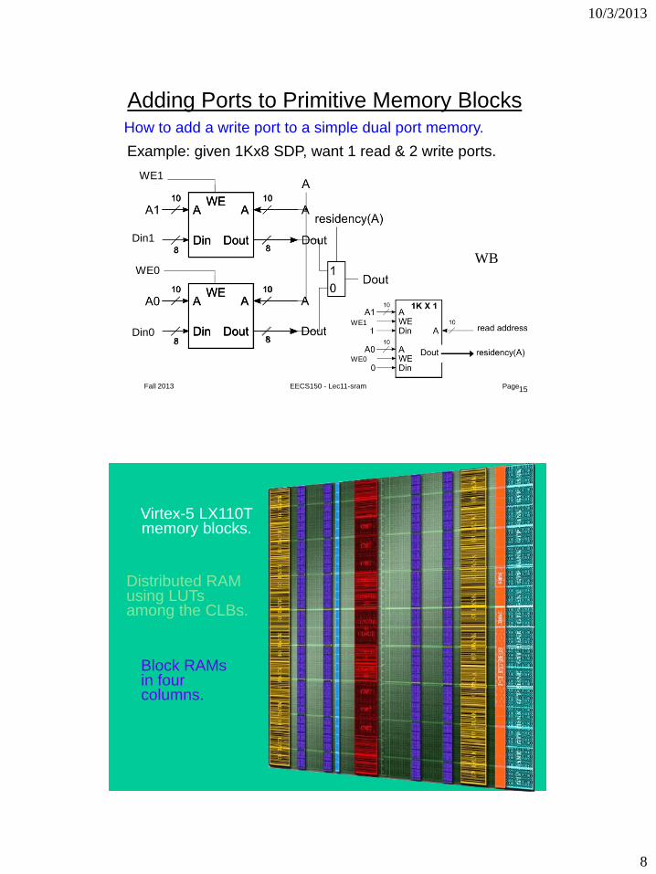
14 Fall 2013 EECS150 - Lec11-sram Page
Adding Ports to Primitive Memory Blocks Adding a read port to a simple dual port (SDP) memory.
Example: given 1Kx8 SDP, want 1 write & 2 read ports.
10/3/2013
8
15 Fall 2013 EECS150 - Lec11-sram Page
Adding Ports to Primitive Memory Blocks How to add a write port to a simple dual port memory.
Example: given 1Kx8 SDP, want 1 read & 2 write ports.
WE1
WB WE0
Din1
Din0
WE1
WE0
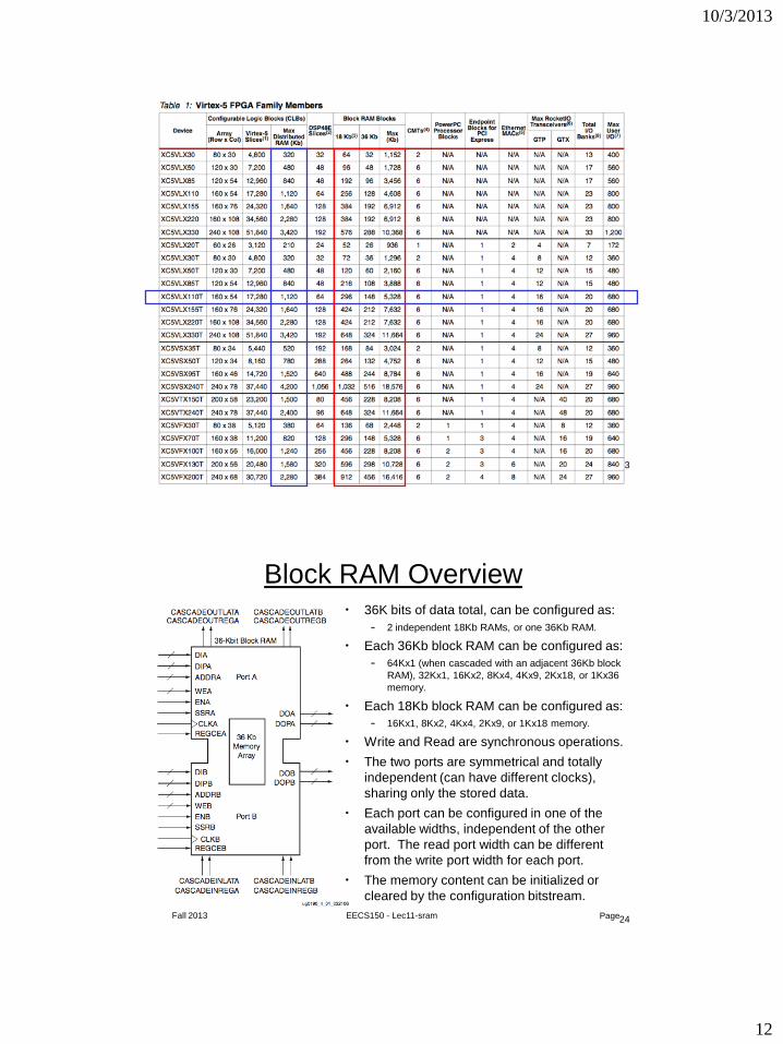
Virtex-5 LX110T memory blocks.
Block RAMs in four columns.
Distributed RAM using LUTs among the CLBs.
10/3/2013
9
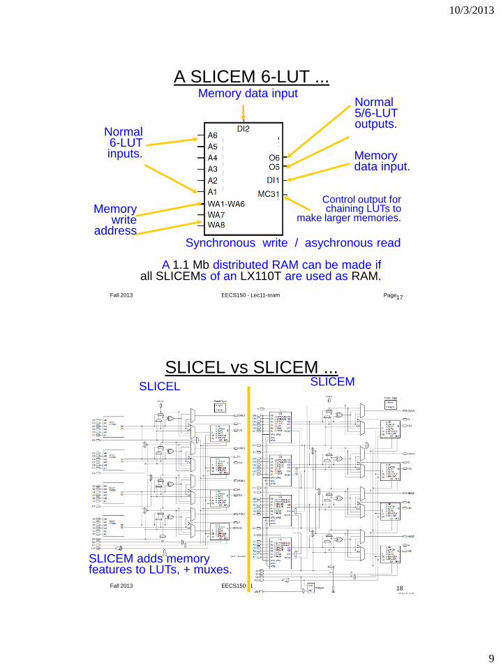
17 Fall 2013 EECS150 - Lec11-sram Page
A SLICEM 6-LUT ...
Normal 6-LUT inputs.
Normal 5/6-LUT outputs.
Memory write
address
Memory data input
Memory data input.
Control output for chaining LUTs to
make larger memories.
A 1.1 Mb distributed RAM can be made if all SLICEMs of an LX110T are used as RAM.
Synchronous write / asychronous read
18 Fall 2013 EECS150 - Lec11-sram Page
SLICEL vs SLICEM ... SLICEM SLICEL
SLICEM adds memory features to LUTs, + muxes.
18
10/3/2013
10
19 Fall 2013 EECS150 - Lec11-sram Page
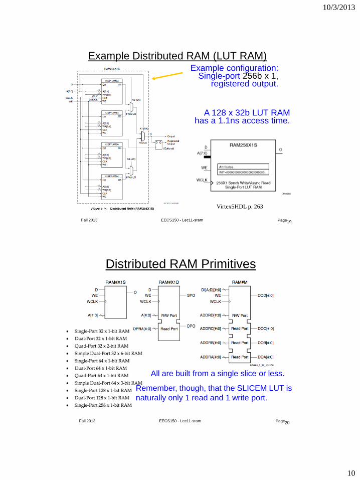
Example Distributed RAM (LUT RAM) Example configuration:
Single-port 256b x 1, registered output.
A 128 x 32b LUT RAM has a 1.1ns access time.
Virtex5HDL p. 263
20 Fall 2013 EECS150 - Lec11-sram Page
Distributed RAM Primitives
All are built from a single slice or less.
Remember, though, that the SLICEM LUT is
naturally only 1 read and 1 write port.
10/3/2013
11
21 Fall 2013 EECS150 - Lec11-sram Page
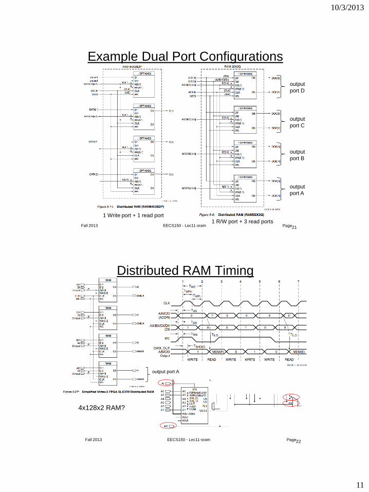
Example Dual Port Configurations
output
port C
output
port B
output
port A
output
port D
1 R/W port + 3 read ports 1 Write port + 1 read port
22 Fall 2013 EECS150 - Lec11-sram Page
Distributed RAM Timing
4x128x2 RAM?
output port A
10/3/2013
12
23 Fall 2013 EECS150 - Lec11-sram Page
24 Fall 2013 EECS150 - Lec11-sram Page
Block RAM Overview • 36K bits of data total, can be configured as:
– 2 independent 18Kb RAMs, or one 36Kb RAM.
• Each 36Kb block RAM can be configured as:
– 64Kx1 (when cascaded with an adjacent 36Kb block
RAM), 32Kx1, 16Kx2, 8Kx4, 4Kx9, 2Kx18, or 1Kx36
memory.
• Each 18Kb block RAM can be configured as:
– 16Kx1, 8Kx2, 4Kx4, 2Kx9, or 1Kx18 memory.
• Write and Read are synchronous operations.
• The two ports are symmetrical and totally
independent (can have different clocks),
sharing only the stored data.
• Each port can be configured in one of the
available widths, independent of the other
port. The read port width can be different
from the write port width for each port.
• The memory content can be initialized or
cleared by the configuration bitstream.

10/3/2013
13
25 Fall 2013 EECS150 - Lec11-sram Page
Block RAM Timing
• Note this is in the default mode, “WRITE_FIRST”. Other
possible modes are “READ_FIRST”, and “NO_CHANGE”.
• Optional output register, would delay appearance of output
data by one cycle.
• Maximum clock rate, roughly 400MHz.
26 Fall 2013 EECS150 - Lec11-sram Page
Verilog Synthesis Notes • Block RAMS and LUT RAMS all exist as primitive library elements.
However, it is much more convenient to use inference.
• Depending on how you write your verilog, you will get either a collection of block RAMs, a collection of LUT RAMs, or a collection of flip-flops.
• The synthesizer uses size, and read style (synch versus asynch) to determine the best primitive type to use.
• It is possible to force mapping to a particular primitive by using synthesis directives. However, if you write your verilog correctly, you will not need to use directives.
• The synthesizer has limited capabilities (eg., it can combine primitives for more depth and width, but is limited on porting options). Be careful, as you might not get what you want.
• See XST User Guide for examples. (p. 126-152)
10/3/2013
14
27 Fall 2013 EECS150 - Lec11-sram Page
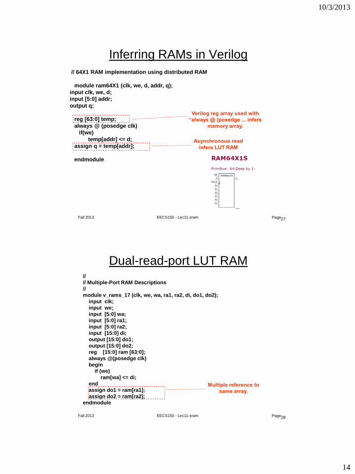
Inferring RAMs in Verilog
// 64X1 RAM implementation using distributed RAM
module ram64X1 (clk, we, d, addr, q);
input clk, we, d;
input [5:0] addr;
output q;
reg [63:0] temp;
always @ (posedge clk)
if(we)
temp[addr] <= d;
assign q = temp[addr];
endmodule
Asynchronous read
infers LUT RAM
Verilog reg array used with
“always @ (posedge ... infers
memory array.
28 Fall 2013 EECS150 - Lec11-sram Page
Dual-read-port LUT RAM //
// Multiple-Port RAM Descriptions
//
module v_rams_17 (clk, we, wa, ra1, ra2, di, do1, do2);
input clk;
input we;
input [5:0] wa;
input [5:0] ra1;
input [5:0] ra2;
input [15:0] di;
output [15:0] do1;
output [15:0] do2;
reg [15:0] ram [63:0];
always @(posedge clk)
begin
if (we)
ram[wa] <= di;
end
assign do1 = ram[ra1];
assign do2 = ram[ra2];
endmodule
Multiple reference to
same array.

10/3/2013
15
29 Fall 2013 EECS150 - Lec11-sram Page
Block RAM Inference //
// Single-Port RAM with Synchronous Read
//
module v_rams_07 (clk, we, a, di, do);
input clk;
input we;
input [5:0] a;
input [15:0] di;
output [15:0] do;
reg [15:0] ram [63:0];
reg [5:0] read_a;
always @(posedge clk) begin
if (we)
ram[a] <= di;
read_a <= a;
end
assign do = ram[read_a];
endmodule
Synchronous read
(registered read address)
infers Block RAM
30 Fall 2013 EECS150 - Lec11-sram Page
Block RAM initialization module RAMB4_S4 (data_out, ADDR, data_in, CLK, WE);
output[3:0] data_out;
input [2:0] ADDR;
input [3:0] data_in;
input CLK, WE;
reg [3:0] mem [7:0];
reg [3:0] read_addr;
initial
begin
$readmemb("data.dat", mem);
end
always@(posedge CLK)
read_addr <= ADDR;
assign data_out = mem[read_addr];
always @(posedge CLK)
if (WE) mem[ADDR] = data_in;
endmodule
“data.dat” contains initial RAM
contents, it gets put into the bitfile
and loaded at configuration time.
(Remake bits to change contents)
10/3/2013
16
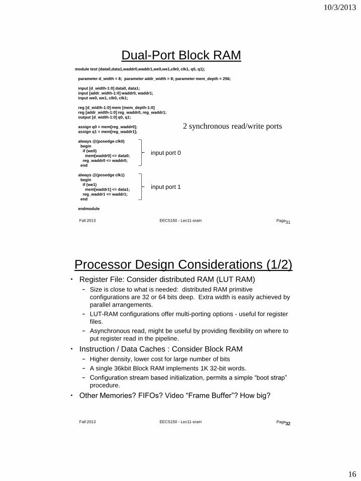
31 Fall 2013 EECS150 - Lec11-sram Page
Dual-Port Block RAM module test (data0,data1,waddr0,waddr1,we0,we1,clk0, clk1, q0, q1);
parameter d_width = 8; parameter addr_width = 8; parameter mem_depth = 256;
input [d_width-1:0] data0, data1;
input [addr_width-1:0] waddr0, waddr1;
input we0, we1, clk0, clk1;
reg [d_width-1:0] mem [mem_depth-1:0]
reg [addr_width-1:0] reg_waddr0, reg_waddr1;
output [d_width-1:0] q0, q1;
assign q0 = mem[reg_waddr0];
assign q1 = mem[reg_waddr1];
always @(posedge clk0)
begin
if (we0)
mem[waddr0] <= data0;
reg_waddr0 <= waddr0;
end
always @(posedge clk1)
begin
if (we1)
mem[waddr1] <= data1;
reg_waddr1 <= waddr1;
end
endmodule
input port 0
input port 1
2 synchronous read/write ports
32 Fall 2013 EECS150 - Lec11-sram Page
Processor Design Considerations (1/2) • Register File: Consider distributed RAM (LUT RAM)
– Size is close to what is needed: distributed RAM primitive
configurations are 32 or 64 bits deep. Extra width is easily achieved by
parallel arrangements.
– LUT-RAM configurations offer multi-porting options - useful for register
files.
– Asynchronous read, might be useful by providing flexibility on where to
put register read in the pipeline.
• Instruction / Data Caches : Consider Block RAM
– Higher density, lower cost for large number of bits
– A single 36kbit Block RAM implements 1K 32-bit words.
– Configuration stream based initialization, permits a simple “boot strap”
procedure.
• Other Memories? FIFOs? Video “Frame Buffer”? How big?
32
10/3/2013
17
33 Fall 2013 EECS150 - Lec11-sram Page
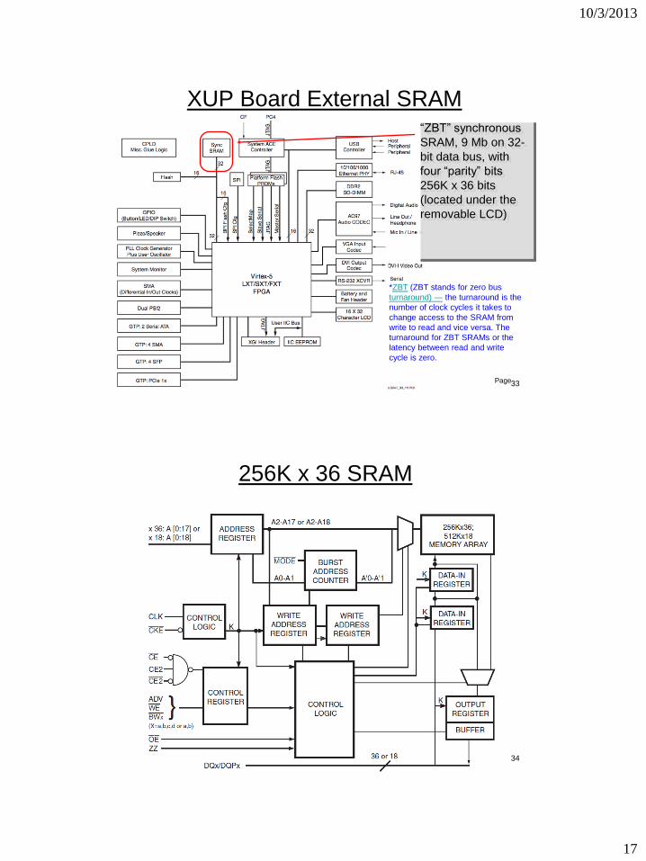
XUP Board External SRAM
More generally, how does software
interface to I/O devices?
*ZBT (ZBT stands for zero bus
turnaround) — the turnaround is the
number of clock cycles it takes to
change access to the SRAM from
write to read and vice versa. The
turnaround for ZBT SRAMs or the
latency between read and write
cycle is zero.
“ZBT” synchronous
SRAM, 9 Mb on 32-
bit data bus, with
four “parity” bits
256K x 36 bits
(located under the
removable LCD)
256K x 36 SRAM
34

10/3/2013
18
35 Fall 2013 EECS150 - Lec11-sram Page
XUP Board External DRAM
More generally, how does software
interface to I/O devices?
*SO-DIMM stands for small outline
dual in-line memory module. SO-
DIMMS are often used in systems
which have space restrictions such
as notebooks.
*DDR2 stands for second
generation double data rate. DDR
transfers data both on the rising and
falling edges of the clock signal.
256 MByte DDR2
DRAM with 400MHz
data rate.
Conclusion
• RAM: single, dual ported
• SliceM RAM and Block RAM
• getting Verilog to give the right kind of RAM
• external RAM
36