eee 211 microwave engineering - athena.ecs.csus.edu
TRANSCRIPT

EEE 211 Microwave Engineering
4. September, 2012

Chapter 1
Introduction to Waves
1.1 Sinusoidal Signals
Sinusoidal signals are important because all periodic signals can be represented with sinusoidal signals ofdifferent amplitudes and phases using Fourier series.
Typical sinusoidal signal is shown in Figure 1.1. On the y-axis is the instantaneous value of the sinusoidalvoltage and on the x-axis is time. Instantaneous values of voltage change from -1V to 1V with time.Sinusoidal signals can be characterized by the following parameters: peak amplitude, peak-to-peak, average,rms, period, time-delay and phase. Peak amplitude, peak-to-peak, average and rms values, are read on they-axis in Figure 1.1, whereas period, time delay and phase are read on the x-axis.
1. Peak amplitude is measured on the y-axis as the length from the average value of the signal (in thiscase zero) to the maximum value of the signal (in this case 1). For signal shown in Figure 1.1, peakamplitude has a constant value of Vp = 1. Peak amplitude is NOT an instantaneous value of the signal,and it does not vary with time. Sometimes amplitude and peak-amplitude are used interchangeably.Other times, amplitude is used to denote an instantaneous value of the signal, and peak-amplitude ismeant to denote the maximum value of amplitude. We will use amplitude to mean peak-amplitude.When we want to emphasize an instantaneous value of the signal, we will call it an instantaneousvalue.
2. Peak-to-peak is measured from the minimum value of the function (in this case -1) to the maximumvalue of the function (in this case 1). For signal shown in Figure 1.1, peak-to-peak voltage has aconstant value of Vpp = 2.
3. RMS or root-mean-square is defined as vrms = 1T
√∫ T0 v(t)2dt. For signal shown in Figure 1.1, and
other sinusoidal signals of this form, vrms =Vp√
2= 1√
2= 0.707. Root mean square value is important
because it represents the equivalent amount of DC power.
4. Average value vave1 = 1T
∫ T0 v(t)dt. For signal shown in Figure 1.1, average value is Vave1 = 0 because
the function has the same area under the function in the positive and negative cycle.
5. Period is measured on the x-axis as the length of one full cycle of the sinusoidal signal. For signalshown in Figure 1.1, this value is period = T
1

Dr. Milica Markovic Microwave Engineering page 2
6. Time delay represents the lag (or lead) of one function with respect to another. For example, in Figure1.1, function cos(ωt−90o) is time-delayed for τ = T
4 with respect to cos(ωt). To find the time delay fora sinusoidal signal from its phase, we look at the way to represent the phase 90o in terms of productof frequency and time. Since in the sinusoidal signal expression cos(ωt + Θ) phase Θ is added to ωtterm, the phase has the same units as ωt, and can be represented as the product of ωτ = θ, τ = θ
ω ,where τ represents the time delay.
7. Phase of the signal is shown in Figure 1.2(d)-(e).
Review signals shown in Figure 1.2. Signals in Figure 1.2(a)-(b) are shown as a function of time, whereassignals in Figure 1.2(c)-(d) are shown as a function of angle. See how are the graphs the same and how arethey different.
Figure 1.1: Vocabulary used in describing sinusoidal signals.
California State University Sacramento EEE211 revised: 4. September, 2012

Dr. Milica Markovic Microwave Engineering page 3
(a) sin(ωt) (b) Sinusoidal signal shifted for time delay −π/4ω
(c) Sinusoidal signal as a function of angle ωt (d) Sinusoidal signal as a function of angle ωt with aphase shift of −π/4
(e) Sinusoidal signal as a function of angle ωt with aphase shift of +π/4
Figure 1.2: Sinusoidal signal as a function of time (a)-(b) and angle (c)-(e).
California State University Sacramento EEE211 revised: 4. September, 2012

Dr. Milica Markovic Microwave Engineering page 4
(a) Sinusoidal signals of different frequencies sin(ωt) (b) Sinusoidal signals of different amplitudes sin(ωt)
Figure 1.3: Comparison of sinusoidal signals.
1.2 Decibels
We will often represent the ratio off the to voltages in decibels. Decibel is a unit that is derived from theunit Bell. Bells are describing an order of magnitude difference between two values. For example, oneBell represents the ratio of 10. 1B = logP1
P2. This ratio is too large to represent quantities in microwave
engineering. Decibel is defined as the ratio of two powers 10 log P1P2
. For example if we want to say that theoutput power is twice the input power we say that the power gain is 3dB.
G = 10logPoutPin
G = 10 log 2
G = 3dB (1.1)
The ratio of voltages is derived from the definition above, because voltages are proportional to power.
G = 10 logV 2out
V 2in
G = 20 logVoutVin
(1.2)
if the output voltage is 1.4 times the input voltage the voltage gain is equal to 3dB, which representsthe power ratio of two.
1.3 Review of complex numbers
1. A complex number z can be represented in Cartesian coordinate system, Equation 1.3 or Polar coor-dinate system, Equation 1.4 form.
California State University Sacramento EEE211 revised: 4. September, 2012

Dr. Milica Markovic Microwave Engineering page 5
Figure 1.4: Complex number z in rectangular and polar coordinates.
z = x+ jy (1.3)
z = |z|ejΘ (1.4)
x is the real part, y is the imaginary part, |z| is the magnitude and Θ is the angle of the complexnumber. Note that we can represent this complex number as a vector.
2. Euler’s Identity is used to convert time domain signal to phasors.
ejΘ = cosΘ + jsinΘ (1.5)
3. Cartesian and polar form representation are used in phasors.
|z| =√x2 + y2 (1.6)
Θ = arctgy
x(1.7)
4. Complex Conjugate is often seen when finding the conditions for maximum power transfer.
z∗ = (x+ jy)∗ = x− jy = |z|e−jΘ (1.8)
5. Complex number addition and subtraction is often seen went to complex impedances are placed inseries and the equivalent complex impedance has to be found. the easiest way to add two complexnumbers is to find Cartesian representation of both and then add the real parts separately and theimaginary part separately.
z1 = x1 + jy1 (1.9)
z2 = x2 + jy2 (1.10)
z1 + z2 = x1 + x2 + j(y1 + y2) (1.11)
California State University Sacramento EEE211 revised: 4. September, 2012

Dr. Milica Markovic Microwave Engineering page 6
6. Multiplication and Division are often seen the in calculation of the transfer function of a circuit. Theeasiest way to divide two complex numbers is to find the polar representation of both and then dividethe amplitudes and subtract the phases.
z1 = |z1|ejΘ1 (1.12)
z2 = |z2|ejΘ2 (1.13)
z1
z2=|z1||z2|
ejΘ1−Θ2 (1.14)
7. Some examples. Find the magnitude and phase of a complex number
−1 = ej180o (1.15)
j = ej90o (1.16)
(1.17)
1.3.1 Phasors
The learning objective of this section is to show how to solve a circuit in frequency domain using phasors.we will review of fat phasers with an RC circuit example shown in Figure 1.6. To solve this circuit in thetime domain we apply Kirchoff’s voltage law as shown in Equation 1.18 -1.19.
The circuit in Figure 1.6 is a simple RC circuit. KVL equation in the time domain is given in Equation1.18.
vs(t) = vR(t) + vC(t) (1.18)
vs(t) = Ri+1
C
∫i(t)dt (1.19)
Figure 1.5: Complex number z in rectangular and polar coordinates.
Where
vs(t) = Acos(ωt+ Θ) (1.20)
In order to solve this circuit we have to solve a differential equation. Use of phasors simplify the equationssignificantly. Differential equations become a set of linear equations. Phasor is another name for a complexnumber in polar coordinate system.
California State University Sacramento EEE211 revised: 4. September, 2012

Dr. Milica Markovic Microwave Engineering page 7
In order to use phasors, the circuit has to be linear. Circuits that have only capacitors, inductors andresistors are linear circuits. In a linear circuit, all currents and voltages are at the frequency of the generator.That means that we don’t have to keep track of the frequency of voltages and currents when we are solvingthe circuit. We know the frequency once we know the frequency of the generator. The quantities that willdiffer for different currents and voltages is the amplitude and phase of the signal. Phasors allow us to dropthe information about the frequency of the signal, and only keep track of the magnitude and phase of thesignal. In order to remove cos(ωt) term from the equations we have to use complex numbers. To writecos(ωt) 1 in a concise form as a complex number, we add to the forcing function a sinusoidal imaginaryterm.
A cos(ωt+ Θ) + jAsin(ωt+ Θ) (1.21)
We have to make sure later when we are done with our calculations with complex number, that we onlytake the real part of the final expression. It seems that we made the above expression more complicated,however, if we remember Euler’s identity, the expression becomes
vs(t) = V cos(ωt+ ΘV ) = ReAcos(ωt+ Θ) + jAsin(ωt+ Θ) = ReAej(ωt+Θ) = ReAejΘejωt (1.22)
In Equation 1.22 we extracted the phase and amplitude information and separated it from the frequency.The amplitude and phase information is called phasor VS(jω) = AejΘ. Why is this expression better thenthe one with a cos(ωt) and how can we remove t from Equation 1.19? To answer this question, we first haveto write general expressions for voltage v(t) and current i(t) in the Equation 1.19:
v(t) = ReV cos(ωt+ ΘV ) + jV sin(ωt+ ΘV ) = ReV ej(ωt+ΘV ) = ReV ejΘV ejωt (1.23)
If we look at the first and last expression in Equation 1.23 we see that the time domain signal is the realpart of the product of phasor and the ejωt term.
v(t) = ReV ejΘV ejωt (1.24)
Similarly for current
i(t) = I cos(ωt+ ΘI) = ReIcos(ωt+ ΘI) + jI sin(ωt+ ΘI) = ReIej(ωt+ΘI) = ReIejΘIejωt (1.25)
If we look at the first and last expression in Equation 1.25 we get a similar expression for current.
i(t) = ReIejΘIejωt (1.26)
In Equations 1.23-1.25 V and I are voltage and current amplitudes, and ΘV and ΘI are voltage andcurrent phases. The voltage on the resistor is then given in Equation 1.27
1It is customary to use cos(ωt) for our time-domain signal. If signals in a circuit are given in terms of sin(ωt), the sin functionhas to be converted to a cosine. To do that, subtract 90o from the phase of the sinusoid, because sin(ωt) = cos(ωt− 90o)
California State University Sacramento EEE211 revised: 4. September, 2012

Dr. Milica Markovic Microwave Engineering page 8
vR(t) = R× i(t) = R×ReIejΘIejωt = ReR× IejΘIejωt (1.27)
The voltage on the capacitor is a bit more complicated. We know that i(t) = ReIejΘIejωt, but whatis the integral of i(t)?
vC(t) =1
C
∫ReIejΘIejωtdt (1.28)
Now if integral and Re exchange places, and if we take all time-independent quantities in front of theintegral,
vC(t) =1
C
∫i(t)dt = Re 1
C
∫IejΘIejωtdt = Re 1
CIejΘI
∫ejωtdt (1.29)
vC(t) = Re 1
CIejΘI
1
jωejωt = Re 1
jωCIejΘIejωt (1.30)
We now replace the time-domain quantities in equation 1.19 with these newly developed expressions.
vs(t) = vR(t) + vC(t) (1.31)
ReAejΘejωt = ReR× IejΘIejωt+Re 1
jωCIejΘIejωt (1.32)
A common term in the previous equation is ejωt, and we can now drop Re, as long as we later rememberto take only the real part of the expresion for the phasor of voltage and current to get the time domainexpression. We can now write the equation as
VSejΘVS = R× IejΘI +
1
jωCIejΘI (1.33)
VS(jω) = RI(jω) +I(jω)
jωC(1.34)
Since this is a linear equation, we can easily solve it:
I(jω) =VS(jω)
R+ 1jωC
(1.35)
Let’s say that the values are given for R, C, ω and VS such that the phasor of the current is I = 3ej45o .To obtain the signal in the time domain, we multiply the phasor I with the ejωt term, and then we find thereal part of the expression to obtain its current in the time domain, as shown in Figure 1.36
i(t) = Re3ej45oejωt = Re3ejωt+45o = Re3 cos(ωt+ 45o) + j3 sin(ωt+ 45o = 3 cos(ωt+ 45o) (1.36)
In case we have an inductor in the circuit, the voltage on an inductor can be derived as shown in Figure1.37.
California State University Sacramento EEE211 revised: 4. September, 2012

Dr. Milica Markovic Microwave Engineering page 9
Figure 1.6: Complex number z in rectangular and polar coordinates.
cicruit element impedance low frequencies f → 0 high frequencies f → inf
capacitor 1jωC ∞ 0
inductor jωL 0 ∞
Table 1.1: Impedance of the capacitor and inductors and their equivalent impedances at high and lowfrequencies.
vL(t) = L∂i(t)
∂t= L
ReIejΘIejωt∂t
dt = ReLIejΘI ∂ejωt
∂t = ReLIejΘI jωejωt = RejωLIejΘIejωt(1.37)
Step-by-step instructions on how to solve circuits using phasors is given as follows:
1. Adopt cosine reference for generator voltage or current.
2. replace all impedances with their phasor expressions,
3. write KVL and KCL, or use other Network Analysis techniques.
4. find the phasor expression for the required current or voltage.
5. multiply the phasor with ejωt
6. find the real part of the above expression to get the current in the time domain.
1.4 Using Vectors to Represent Phasors in an example
1. Calculate on paper the magnitude and phase of the current and voltages in a series RC circuit shownin Figure 1.7 (a) if the circuit is driven with a frequency of 1 GHz (phase is zero) and R=1kΩ, C=1
2π10−12
F.
(a) What are the magnitude, phase and time delay of the source voltage?
(b) What are the magnitude, phase and time delay of the voltage across the resistor?
(c) What are the magnitude, phase and time delay of the voltage across the capacitor?
(d) The simulated voltage across the resistor is about 0.5V and the simulated voltage across thecapacitor is about 0.85V. If we use KVL 0.85V + 0.5V 6= 1V . Why? Look at Figure 1.7 to helpyou with answer this question.
California State University Sacramento EEE211 revised: 4. September, 2012

Dr. Milica Markovic Microwave Engineering page 10
(a) RC circuit in ADS (b) Sinusoidal signal as a function of angle ωt
(c) Points represent polar plot of complexvoltages in RC circuit.
(d) Vectors are drawn in the polar plot ofcomplex voltages in RC circuit. Note howthey add up to 1V.
Figure 1.7: Adding phasors using vectors.
(e) If you know the current through circuit, capacitance, resistance and the frequency of operation,could you plot the phasor diagram to find the input voltage? How would you differentiate betweenthe voltage on an inductor and a capacitor?
California State University Sacramento EEE211 revised: 4. September, 2012

Chapter 2
Transmission Lines
2.1 Introduction to Transmission Lines
Any wire, cable or line that guides energy from one point to another is a transmission line. Whenever youmake a circuit on a breadboard, every wire you attach makes a transmission line with the ground wire.Whether we see the propagation (transmission line) effects on the line depends on the line length. At lowerfrequencies or very short line lengths we do not see any difference between the signal’s phase at the generatorand at the load, whereas at higher frequencies we do.
2.1.1 Types of transmission lines
1. Coaxial Cable, Figure 2.1(a)
2. Microstrip, Figure 2.1(b)
3. Stripline, Figure 2.1(c)
4. Coplanar Waveguide, Figure 2.1(d)
5. Two-wire line, Figure 2.1(e)
6. Parallel Plate Waveguide, Figure 2.1(f)
7. Rectangular Waveguide, Figure 2.1(g)
8. Optical fiber, Figure 2.1(h)
2.1.2 What are Transmission Line Effects?
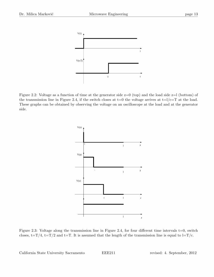
Figure 2.2 shows a step voltage at the generator and the load of a circuit in Figure 2.4. The voltage needsT sec to appear at the load, once the switch closes. Figure 2.3 shows the step signal as it traveles on thetransmission line at different time steps t=0, t=T/4, t=T/2 and t=T. How much time it takes for thissignal to go from AA’ end to BB’ end? Since electromagnetic waves propagate with the constant speed, thespeed of light, time that the signal needs to go from the generator to the load depends on the length of thetransmission line l. T = l
c , where c = 3 108. If the signal at the generator AA’ is
11

Dr. Milica Markovic Microwave Engineering page 12
(a) Coaxial Cable (b) Microstrip (c) Stripline
(d) CoplanarWaveguide
(e) Two-wire Line
(f) Parallel PlateWaveguide
(g) Rectangu-lar Waveguide
(h) Optical Fiber
Figure 2.1: Types of transmission lines.
vAA‘(t) = Acos(ωt) (2.1)
Then at the other end the transmission line the signal is
vBB‘(t) = vAA‘(t− T ) (2.2)
vBB‘(t) = vAA‘(t−l
c) (2.3)
vBB‘(t) = Acos(ω(t− l
c)) (2.4)
vBB‘(t) = Acos(ωt− ω lc) (2.5)
vBB‘(t) = Acos(ωt− ω
cl) (2.6)
Since we know that angular frequency is ω = 2πf
vBB‘(t) = Acos(ωt− 2πf
cl) (2.7)
The quantity cf is called the wavelength λ.
California State University Sacramento EEE211 revised: 4. September, 2012
Dr. Milica Markovic Microwave Engineering page 13
Figure 2.2: Voltage as a function of time at the generator side z=0 (top) and the load side z=l (bottom) ofthe transmission line in Figure 2.4, if the switch closes at t=0 the voltage arrives at t=l/c=T at the load.These graphs can be obtained by observing the voltage on an oscilloscope at the load and at the generatorside.
Figure 2.3: Voltage along the transmission line in Figure 2.4, for four different time intervals t=0, switchcloses, t=T/4, t=T/2 and t=T. It is assumed that the length of the transmission line is equal to l=T/c.
California State University Sacramento EEE211 revised: 4. September, 2012

Dr. Milica Markovic Microwave Engineering page 14
Figure 2.4: Electronic Circuit with an emphasis on cables that connect the generator and the load.
vBB‘(t) = Acos(ωt− 2π
λl) (2.8)
The quantity 2πλ is the propagation constant β
Finally the expression for the voltage at BB end is
vBB‘(t) = Acos(ωt− βl) (2.9)
vBB‘(t) = Acos(ωt−Ψ) (2.10)
We see that at BB’ the signal will experience a phase shift. We will derive this equation again later fromthe Telegrapher’s equations. Now let’s see how the length of the line l affects the voltage at the end BB’.Look at Equation 2.8. The signal will experience a phase shift of 2π l
λ . If this phase shift is small, therewill not be much difference between the phase of the signal at the generator and at the load. This meansthat we don’t have to use transmission line theory to account for the effects of the line. If the phase shift issignificant, then we do have to use the transmission line theory. Let’s look at some numbers in the followingexample.
1. If lλ < 0.01 then the angle 2π l
λ is of the order of 0.0314 rad or about 20. In this case, the phase isobviosly something that we don’t have to worry about. When the length of the transmission line ismuch smaller than λ, l << λ
100 the wave propagation on the line can be ingnored.
2. If lλ > 0.01, say l
λ = 0.1, then the phase is 200, which is a significant phase shift. In this case it maybe necessary to account fro transmission line effects.
2.1.3 Propagation modes on a transmission line
Coax, two wire line, microstrip etc can be approximated as TEM up to the 30-40 GHz (unshielded), up to140 GHz shielded.
1. TEM E, M field is entirely transverse to the direction of propagation
2. TE, TM E or M field is in the direction of propagation
Transmission lines that we are discussing here are TEM lines.
California State University Sacramento EEE211 revised: 4. September, 2012

Dr. Milica Markovic Microwave Engineering page 15
2.2 Wave equation on a transmission line
In this section we will derive the expression for voltage and current along a transmission line. This expressionwill have two variables, time t and space z. So far we have only seen voltages and currents as a functionof time. This is because all circuit elements seen so far were lumped elements. In distributed systems wewant to derive the equations for voltage and current for the case when the transmission line is longer thenthe fraction of a wavelength. To make sure that we don’t encounter any transmission line effects to startwith, we can look at the piece of a transmission line that is much smaller then the fraction of a wavelength.In other words we cut the transmission line into small pieces to make sure there are no transmission lineeffects, as the pieces are shorter then the fraction of a wavelength. We then represent each piece with anequivalent circuit as shown in Figure ??. To derive expressions for current and voltage on transmission linewe will use the following five-step plan
1. Look at an infinitesimal length of a transmission line ∆z.
2. Represent that piece with an equivalent circuit.
3. Write KCL, KVL for the piece in the time domain (we get differential equations)
4. Apply phasors (equations become linear)
5. Solve the linear system of equations to get the expression for the voltage and current on the transmis-sion line as a function of z.
Let’s follow the plan now. Look at a small piece of a transmission line and represented it with anequivalent circuit.
Write KVL and KCL equations for the circuit above.KVL
−v(z, t) +R∆zi(z, t) + L∆z∂i(z, t)
∂t+ v(z + ∆z, t) = 0
KCL
i(z, t) = i(z + ∆z) + iCG(z + ∆z, t)
i(z, t) = i(z + ∆z) +G∆zv(z + ∆z, t) + C∆z∂v(z + ∆z, t)
∂t
Rearrange the KCL and KVL Equations 2.11, 2.15 and divide them with ∆z. Equations 2.12, 2.16. let∆z → 0 and recognize the definition of the derivative Equations, 2.13, 2.17.
KVL
−(v(z + ∆z, t)− v(z, t)) = R∆zi(z, t) + L∆z∂i(z, t)
∂t(2.11)
−v(z + ∆z, t)− v(z, t)
∆z= Ri(z, t) + L
∂i(z, t)
∂t(2.12)
lim∆z→0
−v(z + ∆z, t)− v(z, t)
∆z = lim
∆z→0Ri(z, t) + L
∂i(z, t)
∂t (2.13)
−v(z, t)
∂z= Ri(z, t) + L
∂i(z, t)
∂t(2.14)
California State University Sacramento EEE211 revised: 4. September, 2012

Dr. Milica Markovic Microwave Engineering page 16
(a) Coaxial cable is cut in short pieces. (b) Equivalent circuit of a section of trans-mission line.
(c) Equivalent circuit of transmission line.
Figure 2.5: Section of a coaxial cable.
California State University Sacramento EEE211 revised: 4. September, 2012

Dr. Milica Markovic Microwave Engineering page 17
KCL
−(i(z + ∆z, t)− i(z, t)) = G∆zv(z + ∆z, t) + C∆z∂v(z + ∆z, t)
∂t(2.15)
− i(z + ∆z, t)− i(z, t)∆z
= Gv(z + ∆z, t) + C∂v(z + ∆z, t)
∂t(2.16)
lim∆z→0
− i(z + ∆z, t)− i(z, t)∆z
= lim∆z→0
Gv(z + ∆z, t) + C∂v(z + ∆z, t)
∂t (2.17)
− i(z, t)∂z
= Gv(z + ∆z, t) + C∂v(z + ∆z, t)
∂t(2.18)
We just derived Telegrapher’s equations in time-domain:
−v(z, t)
∂z= Ri(z, t) + L
∂i(z, t)
∂t
− i(z, t)∂z
= Gv(z + ∆z, t) + C∂v(z + ∆z, t)
∂t
Telegrapher’s equations are two differential equations with two unknowns, i(z, t), v(z, t). It is not impossibleto solve them, however we would prefer to have linear equations. So what do we do now? Express time-domain variables as phasors!
v(z, t) = ReV (z)ejωti(z, t) = ReI(z)ejωt
And we get the Telegrapher’s equations in phasor form
−∂V (z)
∂z= (R+ jωL)I(z) (2.19)
−∂I(z)
∂z= (G+ jωC)V (z) (2.20)
Two equations, two unknowns. To solve these equations, we first take a derivative of both equationswith respect to z.
−∂2V (z)
∂z2= (R+ jωL)
∂I(z)
∂z(2.21)
−∂2I(z)
∂z2= (G+ jωC)
∂V (z)
∂z(2.22)
Rearange the previous equations:
− 1
(R+ jωL)
∂I(z)
∂z=∂2V (z)
∂z2(2.23)
− 1
(G+ jωC)
∂V (z)
∂z=∂2I(z)
∂z2(2.24)
California State University Sacramento EEE211 revised: 4. September, 2012

Dr. Milica Markovic Microwave Engineering page 18
Substitute Eq.2.23 into Eq.2.20 and Eq.2.24 into Eq.2.19 and we get
−∂2V (z)
∂z2= (G+ jωC)(R+ jωL)V (z) (2.25)
−∂2I(z)
∂z2= (G+ jωC)(R+ jωL)I(z) (2.26)
Or if we rearrange
∂2V (z)
∂z2− (G+ jωC)(R+ jωL)V (z) = 0 (2.27)
∂2I(z)
∂z2− (G+ jωC)(R+ jωL)I(z) = 0 (2.28)
The above Eq.2.27 and Eq.2.28 are called the wave equation, and they represent current and voltagewave on a transmission line. γ = (G+ jωC)(R+ jωL) is the complex propagation constant. This constanthas a real and an imaginary part.
γ = α+ jβ
where α is the attenuation constant and β is the phase constant.
α = Re√
(G+ jωC)(R+ jωL)β = Im
√(G+ jωC)(R+ jωL)
The general solution of the differential equation of the type 2.27 or 2.28? From differential equationclass, we know that the solution to this kind of equation is:
V (z) = V +0 e−γz + V −0 eγz
I(z) = I+0 e−γz + I−0 e
γz
In this equation V +0 and V −0 are the phasors of forward and reflected voltage waves, and I+
0 and I−0are the phasors of forward and reflected current wave. The time domain expression for the current andvoltage on the transmission line we can get by multiplying the phasor of the voltage and current with ejωt
and taking the real part of it.
v(t) = Re(V +0 e(−α−jβ)z + V −0 e(α+jβ)z)ejωt
v(t) = |V +0 |e
−αz cos(ωt− βz + 6 V +0 ) + |V −0 |e
αz cos(ωt+ βz + 6 V −0 ) (2.29)
We’ll look at the Matlab program the next class to see that if the signs of the ωt and βz are the samethe wave moves in the forward +z direction. If the signs of ωt and βz are opposite, the wave moves in the−z direction.
California State University Sacramento EEE211 revised: 4. September, 2012
Dr. Milica Markovic Microwave Engineering page 19
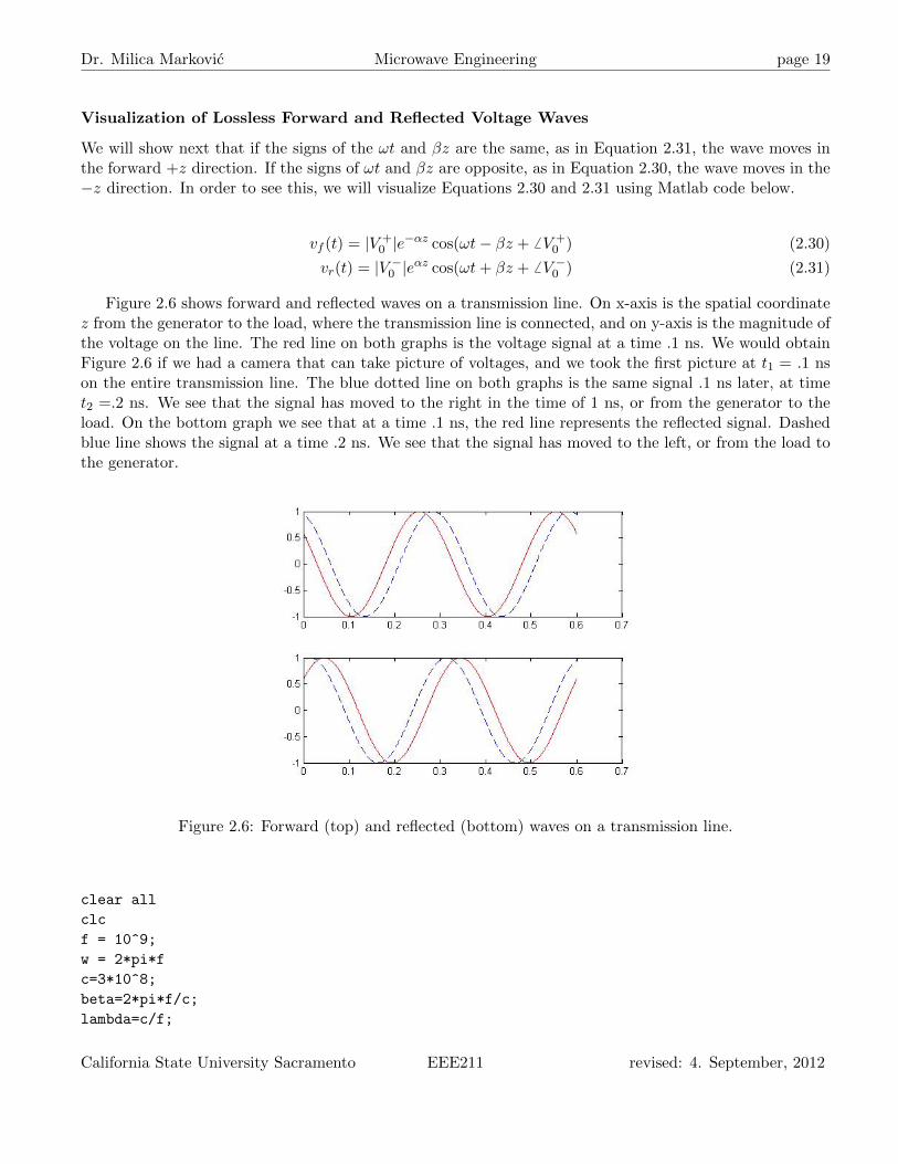
Visualization of Lossless Forward and Reflected Voltage Waves
We will show next that if the signs of the ωt and βz are the same, as in Equation 2.31, the wave moves inthe forward +z direction. If the signs of ωt and βz are opposite, as in Equation 2.30, the wave moves in the−z direction. In order to see this, we will visualize Equations 2.30 and 2.31 using Matlab code below.
vf (t) = |V +0 |e
−αz cos(ωt− βz + 6 V +0 ) (2.30)
vr(t) = |V −0 |eαz cos(ωt+ βz + 6 V −0 ) (2.31)
Figure 2.6 shows forward and reflected waves on a transmission line. On x-axis is the spatial coordinatez from the generator to the load, where the transmission line is connected, and on y-axis is the magnitude ofthe voltage on the line. The red line on both graphs is the voltage signal at a time .1 ns. We would obtainFigure 2.6 if we had a camera that can take picture of voltages, and we took the first picture at t1 = .1 nson the entire transmission line. The blue dotted line on both graphs is the same signal .1 ns later, at timet2 =.2 ns. We see that the signal has moved to the right in the time of 1 ns, or from the generator to theload. On the bottom graph we see that at a time .1 ns, the red line represents the reflected signal. Dashedblue line shows the signal at a time .2 ns. We see that the signal has moved to the left, or from the load tothe generator.
Figure 2.6: Forward (top) and reflected (bottom) waves on a transmission line.
clear all
clc
f = 10^9;
w = 2*pi*f
c=3*10^8;
beta=2*pi*f/c;
lambda=c/f;
California State University Sacramento EEE211 revised: 4. September, 2012

Dr. Milica Markovic Microwave Engineering page 20
t1=0.1*10^(-9)
t2=0.2*10^(-9)
x=0:lambda/20:2*lambda;
y1=sin(w*t1 - beta.*x);
y2=sin(w*t2 - beta.*x);
y3=sin(w*t1 + beta.*x);
y4=sin(w*t2 + beta.*x);
subplot (2,1,1),
plot(x,y1,’r’),...
hold on
plot(x,y2,’--b’),...
hold off
subplot (2,1,2),
plot(x,y3,’r’)
hold on
plot(x,y4,’--b’)
hold off
Visualization of Lossless Forward and Reflected Voltage Waves
Repeat the visualization of signals in the previous section for a lossy transmission line. Assume thatα = 0.1 Np, and all other variables are the same as in the previous section. How do the voltages compare inthe lossy and lossless cases?
2.2.1 Relating forward and backward current and voltage waves on the transmissionline
In equations 2.32-2.33 V +0 and V −0 are the phasors of forward and reflected going voltage waves, and I+
0 andI−0 are the phasors of forward and reflected current waves. In this section, we will see how the phasors offorward and reflected voltage and current waves are related to transmission line impedance.
V (z) = V +0 e−γz + V −0 eγz (2.32)
I(z) = I+0 e−γz + I−0 e
γz (2.33)
When substitute the voltage wave equation into Telegrapher’s Equations ??. The equation is repeatedhere Eq.2.34-2.35.
−∂V (z)
∂z= (R+ jωL)I(z) (2.34)
γV +0 e−γz − γV −0 eγz = (R+ jωL)I(z) (2.35)
We now rearrange Eq.2.35
California State University Sacramento EEE211 revised: 4. September, 2012

Dr. Milica Markovic Microwave Engineering page 21
I(z) =γ
R+ jωL(V +
0 exp−γz + V −0 expγz)
I(z) =γV +
0
R+ jωLe−γz − γV −0
R+ jωLeγz (2.36)
Now we compare Eq.2.36 with the Eq.2.33. In order for two transcendental equations to be equal, thecoefficients next to exponential terms have to be the same.
I+0 =
γV +0
R+ jωL
I−0 = − γV −0R+ jωL
We can define the characteristic impedance of a transmission line as the ratio of the voltage to currentamplitude of the forward going wave.
Z0 =V +
0
I+0
Z0 =R+ jωL
γ
Z0 =
√R+ jωL
G+ jωC
2.2.2 Lossless transmission line
In many practical applications R→ 0 1and G→ 02. This is a lossless transmission line.In this case the transmission line parameters are
• Propagation constant
γ =√
(R+ jωL)(G+ jωC)
γ =√jωLjωC
γ = jω√LC = jβ
• Transmission line impedance
1metal resistance is low2dielectric conductance is low
California State University Sacramento EEE211 revised: 4. September, 2012

Dr. Milica Markovic Microwave Engineering page 22
Z0 =
√R+ jωL
G+ jωC
Z0 =
√jωL
jωC
Z0 =
√L
C
• Wave velocity
v =ω
β
v =ω
ω√LC
v =1√LC
• Wavelength
λ =2π
β
λ =2π
ω√LC
λ =2π
√ε0µ0εr
λ =c
f√εr
λ =λ0√εr
2.3 What does it mean when we say a medium is lossy or lossless?
In a lossless medium electromagnetic wave power is not turning into heat, there is no loss of amplitude. Inlossy medium electromagnetic wave is heating up the medium, therefore its power is decreasing as e−αx.
medium attenuation constant α [dB/km]
coax 60
waveguide 2
fiber-optic 0.5
In guided wave systems such as transmission lines and waveguides the attenuation of power with distancefollows approximately e−2αx. The power radiated by an antenna falls off as 1/r2.
California State University Sacramento EEE211 revised: 4. September, 2012

Dr. Milica Markovic Microwave Engineering page 23
2.3.1 Low-Loss Transmission Line
In some practical applications, losses are small, but not negligible. R << ωL 3and G << ωC4.In this case the transmission line parameters are
• Propagation constant
We can re-write the propagation constant as shown below. In somel applications, losses are small, butnot negligible. R << ωL and G << ωC, then in Equation 2.38, RG << ω2LC.
γ =√
(R+ jωL)(G+ jωC) (2.37)
γ = jω√LC
√1 − j
(R
ωL+
G
ωC
)− RG
ω2LC(2.38)
γ ≈ jω√LC
√1 − j
(R
ωL+
G
ωC
)(2.39)
Taylor’s series for function√
1 + x =√
1 − j(RωL + G
ωC
)in Equation 2.39 is shown in Equations
2.40-2.41.
√1 + x = 1 +
x
2− x2
8+x3
16− ... for |x| < 1 (2.40)
γ ≈ jω√LC
√1 − j
(R
ωL+
G
ωC
)= jω
√LC
(1− j
2
(R
ωL+
G
ωC
))(2.41)
The real and imaginary part of the propagation constant γ are:
α =ω√LC
2
(R
ωL+
G
ωC
)(2.42)
β = ω√LC (2.43)
We see that the phase constant β is the same as in the lossless case, and the attenuation constant αis frequency independent. This means that all frequencies of a modulated signal are attenuated thesame amount, and there is no dispersion on the line. When the phase constant is a linear function offrequency, β = const ω, then the phase velocity is a constant vp = ω
β = 1const , and the group velocity is
also a constant, and equal to the phase velocity. In this case, all frequencies of the modulated signalare propagated with the same speed, and there is no distortion of the signal. This is the case onlywhen the losses in the transmission line are small.
We usually represent phase and group velocity on ω − β diagrams, shown in Figure 2.3.1(a). At afrequency ω1, the ratio of ω
β gives the phase velocity (graphically, this is the slope of the red line on
3metal resistance is lower than the inductive impedance4dielectric conductance is lower than the capacitive impedance
California State University Sacramento EEE211 revised: 4. September, 2012

Dr. Milica Markovic Microwave Engineering page 24
the graph), whereas the slope of the ω − β curve (blue line on the graph) gives the group velocity atthis frequency. These diagrams are useful, as they show how phase constant β varies with frequency,and it also shows how phase and group velocities vary with frequency. We can see that in this case,both group and phase velocity for this line are positive quantities, which is a representation of whatis called a forward wave. In a forward wave, both signal and the energy propagate in the forwarddirection. Backward waves are waves where the signal propagates forward, however energy propagatesbackwards. In backward waves, phase and group velocities have opposite signs.
When the phase constant is a linear function of frequency, then, phase velocity and group velocity areequal, and do not depend on frequency. Both velocities are equal to the slope of the line in Figure2.3.1(b).
(a) Phase constant β is a nonlinearfunction of frequency.
(b) Phase constant β is a linear func-tion of frequency.
Figure 2.7: Omega-Beta diagrams.
2.3.2 Voltage Reflection Coefficient, Lossless Case
The equations for the voltage and current on the transmission line we derived so far are
V (z) = V +0 e−jβz + V −0 ejβz (2.44)
I(z) =V +
0
Z0e−jβz − V −0
Z0ejβz (2.45)
Figure 2.8: Transmission Line connects generator and the load.
At z = 0 the impedance of the load has to be
California State University Sacramento EEE211 revised: 4. September, 2012

Dr. Milica Markovic Microwave Engineering page 25
ZL =V (0)
I0
Substitute the boundary condition in Eq.2.44
ZL = Z0V +
0 + V −0V +
0 − V−
0
(2.46)
We can now solve the above equation for V −0
ZLZ0
(V +0 − V
−0 ) = V +
0 + V −0
(ZLZ0− 1)V +
0 = (ZLZ0
+ 1)V −0
V −0V +
0
=
ZLZ0− 1
ZLZ0
+ 1
V −0V +
0
=ZL − Z0
ZL + Z0(2.47)
The quantityV −0
V +0
is called voltage reflection coefficient Γ. It relates the reflected to incident voltage
phasor. Voltage reflection coefficient is in general a complex number, it has a magnitude and a phase.
Examples
1. 100 Ω transmission line is terminated in a series connection of a 50 Ω resistor and 10 pF capacitor. Thefrequency of operation is 100 MHz. Find the voltage reflection coefficient.
2. For purely reactive load ZL = jXL find the reflection coefficient.
The end of this lecture is spent in the lab making a Matlab program to make a movie of a wave movingleft and right.
2.3.3 Standing Waves
In the previous section we introduced the voltage reflection coefficient that relates the forward to reflectedvoltage phasor.
Γ =V −0V +
0
=ZL − Z0
ZL + Z0(2.48)
If we substitute Equation 2.48 to Eq.2.49 we get for the voltage wave
V (z) = V +0 e−jβz + V −0 ejβz (2.49)
V (z) = V +0 e−jβz + ΓV +
0 ejβz
V (z) = V +0 (e−jβz − Γejβz) (2.50)
California State University Sacramento EEE211 revised: 4. September, 2012

Dr. Milica Markovic Microwave Engineering page 26
since Γ = |Γ|ejΘr Eq.2.51 becomes
V (z) = V +0 (e−jβz − |Γ|ejβz+Θr) (2.51)
and for the current wave
I(z) =V +
0
Z0e−jβz − V −0
Z0ejβz (2.52)
I(z) =V +
0
Z0e−jβz + Γ
V +0
Z0ejβz
I(z) =V +
0
Z0(e−jβz − Γejβz) (2.53)
The voltage and the current waveform on a transmission line are therefore given by Eqns.2.51, 2.53.Now we have two equations and one unknown V +
0 ! We will solve these two equations in Lecture 7. Nowlet’s look at the physical meaning of these equations.
In Eq.2.51, Γ is the voltage reflection coefficient, V +0 is the phasor of the forward going wave, z is the
axis in the direction of wave propagation, β is the phase constant5, Z0 is the impedance of the transmissionline6. V (z) is a complex number, phasor. We will find the magnitude and phase of the voltage on thetransmission line.
The magnitude of a complex number can be found as |z| =√zz∗.
|V (z)| =√V (z)V (z)∗
|V (z)| =√V +
0 (e−jβz − |Γ|ejβz+Θr)V +0 (ejβz − |Γ|e−(jβz+Θr))
|V (z)| = V +0
√(e−jβz − |Γ|ejβz+|Θr)(ejβz − |Γ|e−(jβz+Θr))
|V (z)| = V +0
√1 + |Γ|e−(2jβz+|Θr) + |Γ|ej2βz+Θr + |Γ|2)
|V (z)| = V +0
√1 + |Γ|2 + |Γ|(e−(2jβz+Θr) + e(j2βz+Θr))
|V (z)| = V +0
√1 + |Γ|2 + 2|Γ| cos(2βz + Θr) (2.54)
The magnitude of the total voltage on the transmission line is given by Eq.2.54. It seems like a compli-cated function.
• Let’s start from a simple case when the voltage reflection coefficient on the tranmission line is Γ = 0and draw the magnitude of the total voltage. The magnitude is the green line in Figure 2.9. To see themovie of this transmission line go to the class web page under Instructional Videos. Forward voltageis shown in red, reflected voltage in pink, and the magnitude of the voltage is green. Magnitude of thevoltage is constant everywhere on the transmission line, and so the line is called flat.
5imaginary part of the complex propagation constant6defined as the ratio of forward going voltage and current
California State University Sacramento EEE211 revised: 4. September, 2012

Dr. Milica Markovic Microwave Engineering page 27
Figure 2.9: Flat line.
• Let’s look at another case, Γ = 0.5 and Θr = 0. Equation 2.55 represents the magnitude of the voltageon the transmission line, and Figure 2.10 shows in green how this function looks on a transmissionline. This case is shown in Figure 2.10.
|V (z)| = V +0
√5
4+ cos2βz (2.55)
Figure 2.10: Voltage on a transmission line with reflection coefficient magnitude 0.5, and zero phase.
The function 2.55 is at it’s maximum when cos(2βz) = 1 or z = k2λ, and the function value is
V (z) = 1.5V +0 . It is at it’s minimum when cos(2βz) = −1 or z = 2k+1
4 λ and the function value isV (z) = 0.5V +
0
It is important to mention here that the function that we see looks like a cosine with an average valueof V +
0 , but it is not. The minimums of the function are sharper then the maximums, so when thereflection coefficient is at it’s maximum of Γ = 1 the function looks like this:
• General Case.
In general the voltage maximums will occur when cos(2βz) = 1
California State University Sacramento EEE211 revised: 4. September, 2012

Dr. Milica Markovic Microwave Engineering page 28
Figure 2.11: Shorted Transmission Line.
|V (z)max| = V +0
√1 + |Γ|2 + 2|Γ|
|V (z)max| = V +0
√(1 + |Γ|)2
|V (z)max| = V +0 (1 + |Γ|) (2.56)
In general the voltage minimums will occur when cos(2βz) = −1,
|V (z)min| = V +0
√1 + |Γ|2 − 2|Γ|
|V (z)min| = V +0
√(1− |Γ|)2
|V (z)min| = V +0 (1− |Γ|) (2.57)
The ratio of voltage minimum on the line over the voltage maximum is called the Voltage StandingWave Ratio (VSWR) or just Standing Wave Ratio (SWR).
SWR =V (z)maxV (z)min
SWR =1 + |Γ|1− |Γ|
(2.58)
The voltage maximum position on the line is where
cos(2βz) = 1
2βz + Θr = 2nπ
z =2nπ −Θr
2β
z =2nπ −Θr
4π(2.59)
California State University Sacramento EEE211 revised: 4. September, 2012
Chapter 3
Smith Chart
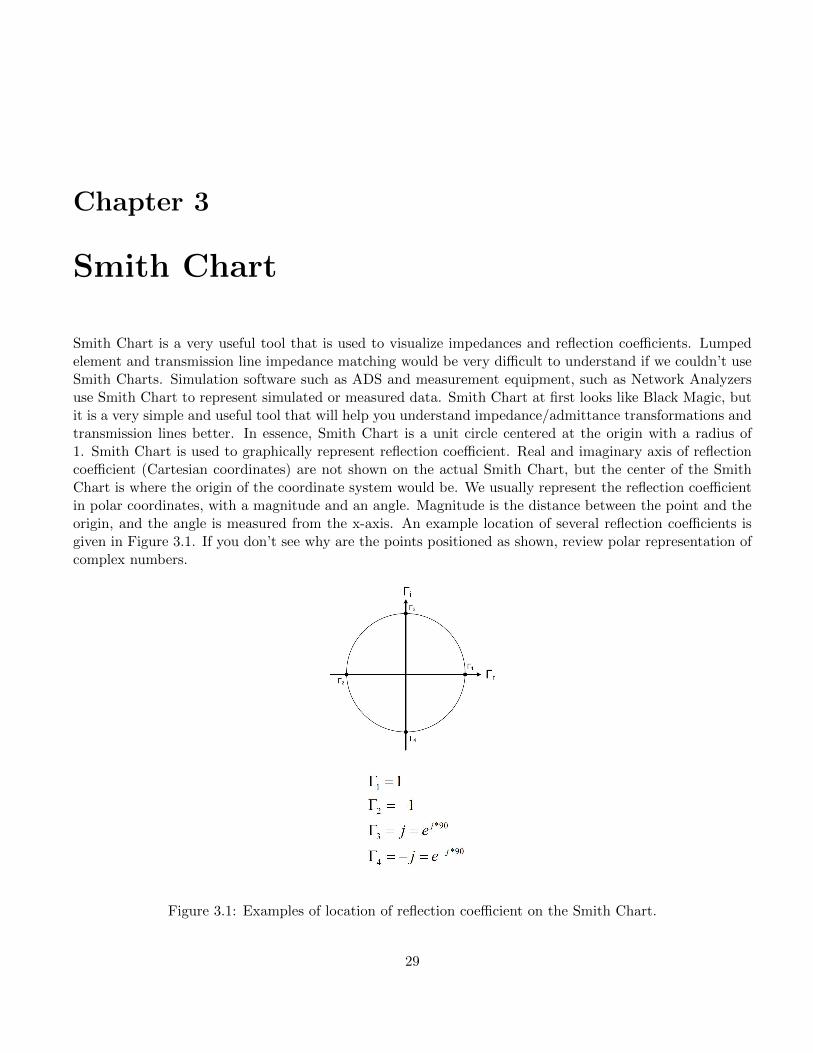
Smith Chart is a very useful tool that is used to visualize impedances and reflection coefficients. Lumpedelement and transmission line impedance matching would be very difficult to understand if we couldn’t useSmith Charts. Simulation software such as ADS and measurement equipment, such as Network Analyzersuse Smith Chart to represent simulated or measured data. Smith Chart at first looks like Black Magic, butit is a very simple and useful tool that will help you understand impedance/admittance transformations andtransmission lines better. In essence, Smith Chart is a unit circle centered at the origin with a radius of1. Smith Chart is used to graphically represent reflection coefficient. Real and imaginary axis of reflectioncoefficient (Cartesian coordinates) are not shown on the actual Smith Chart, but the center of the SmithChart is where the origin of the coordinate system would be. We usually represent the reflection coefficientin polar coordinates, with a magnitude and an angle. Magnitude is the distance between the point and theorigin, and the angle is measured from the x-axis. An example location of several reflection coefficients isgiven in Figure 3.1. If you don’t see why are the points positioned as shown, review polar representation ofcomplex numbers.
Figure 3.1: Examples of location of reflection coefficient on the Smith Chart.
29

Dr. Milica Markovic Microwave Engineering page 30
In Figure 3.2 circle and line shown represent all points on the Smith Chart that have constant magnitudeor angle of the reflection coefficient. At high frequencies it is difficult to measure impedances directly, as itis difficult to measure (or sometimes even define) voltage and current. To measure impedances, engineersuse Network Analyzer shown in Figure 3.3.
(a) |Γ|=0.5, |Γ|=1 (b) < Γ = 45, < Γ = 120
Figure 3.2: Points of constant magnitude (a) of the reflection coefficient and phase (b) of the reflectioncoefficient.
Since reflection coefficient and impedance are related through Equation 3.1, we can find impedance thatcorresponds to the reflection coefficient, Equation 3.2. In other words, every point on the Smith Chartrepresents one reflection coefficient Γ and one impedance ZL.
Γ =ZL − ZZL + Z
(3.1)
zL =ZLZ
=1 + Γ
1− Γ(3.2)
Figure 3.4 shows circles on the Smith Chart that represent constant (normalized) reactances, and resis-tances. Figure 3.5, shows how to find zL = 1 + j1. This impedance is at a point where the circle of constantresistance rL = 1 crosses the circle of constant reactance xL = 1. Figure 3.6 shows how to find the reflectioncoefficient if normalized load impedance zL = 1 + j1 is given. Measure the distance bewteen the originusing the scale ”Reflection Coefficient E or I”on the bottom of the Smith Chart to find the magnitude of thereflection coefficient. To find the angle of the reflection coefficient, we read the scale ”Angle of ReflectionCoefficient” on the perimeter of the Smith Chart, shown in green. The reflection coefficient is therefore0.5ej62o , which is close to the actual value 0.5ej64o . If you have done this using ruler and compass, andnicely sharpened pencil, you would get exactly the right answer. Try it out!
California State University Sacramento EEE211 revised: 4. September, 2012

Dr. Milica Markovic Microwave Engineering page 31
Figure 3.3: HP8510 Network Analyzer in Microwave Laboratory measures impedances up to 26.5GHz. Thispiece of equipment is on permanent loan curtesy of Defense Micro Electronic Activity (DMEA), Sacramento
(a) Normalized resistance circles. (b) Normalized reactance circles.
Figure 3.4: All points on the circle have the constant imaginary part of the impedance.
California State University Sacramento EEE211 revised: 4. September, 2012

Dr. Milica Markovic Microwave Engineering page 32
Figure 3.5: Red circle that represents all points on Smith Chart with normalized resistance r = 1 andblue circle that represents all points on Smith Chart with normalized reactance x = 1 cross at point whereZL = 1 + j1.
Figure 3.6: To find the magnitude of the reflection coefficient from impedance ZL = 1 + j1, we measurethe distance bewteen the origin using the scale ”Reflection Coefficient E or I”on the bottom of the SmithChart. To find the angle of the reflection coefficient, we read the scale ”Angle of Reflection Coefficient” onthe perimeter of the Smith Chart.
California State University Sacramento EEE211 revised: 4. September, 2012

Dr. Milica Markovic Microwave Engineering page 33
Brief review of impedance and admittance
Impedance’s real part is called resistance R, and imaginary part is called reactance X. Admittance’s realpart is called conductance, and imaginary part is called susceptance. It is easier to add impedances whenelements are in series, and it is easier to add admittances when elements are in parallel, see Figure 3.7,because we just add real and imaginary parts separately. This is the reason we have special Smith Chartshown in Figure 3.8 that has both impedance and admittance circles on it. This way, we can use SmithChart to read off the values for equivalent impedance or admittance when we add impedances or admittancesin parallel or series. This comes in handy for lumped-element impedance matching that we will talk aboutnext.
Figure 3.7: It is easier to use admittance when the circuit elements are in parallel and impedance when thecircuit elements are in series.
California State University Sacramento EEE211 revised: 4. September, 2012

Dr. Milica Markovic Microwave Engineering page 34
Figure 3.8: On Smith Chart Best impedances are shown in red, and admittances in green.
3.1 Impedance Matching
Intro to Impedance Matching
Impedance matching is a technique that ensures maximum power transfer between the generator Vg andthe load ZL. The maximum power transfer is achieved when the input impedance looking into the circuitlooking from he generator is a complex conjugate of the impedance of the load. In the case shown in Figure3.9, the impedance of the generator and the line is Z, so to perform maximum power transfer, the inputimpedance of the impedance matching circuit has to be equal to Z. We perform impedance matching toremove the reflected wave on the transmission line, and maximize the power delivery to the load. Whenthere is only the forward wave on the line, the line is called ”flat”, because the magnitude of the forwardwave is the same everywhere on the line (and equal to V +
). When we insert the impedance matching circuitbetween the load ZL and the transmission line Z, the input impedance presented to the generator and thetransmission line from the impedance matching circuit will be Z, and the impedance presented to the loadimpedance ZL will be Z∗L. Our task is therefore to add capacitors and inductors to the load ZL to make theinput impedance look like Z. We do not want to use resistors in an impedance matching circuit becausethey will use some of the power that we need at ZL. If we represent ZL on the Smith Chart Best as a point,our task will be to take that point to the center of the Smith Chart, where the impedance is equal to Z.
3.1.1 Lumped Element Impedance Matching
California State University Sacramento EEE211 revised: 4. September, 2012

Dr. Milica Markovic Microwave Engineering page 35
Figure 3.9: The result of impedance matching.
California State University Sacramento EEE211 revised: 4. September, 2012