eee 41 midterms 1s1314
DESCRIPTION
Semiconductor MidtermsTRANSCRIPT
Instructions:
1. Write your name, section and student number in the space provided.
2. Do not separate the pages of the exam.
3. Make your answers as clear and concise as possible, and also make sure your handwriting is legible. Avoid erasuresand think before you write. Ambiguous answers as well as anything we cannot understand, will be marked wrong.
4. If you have any questions, raise your hand. We will come to you.
5. Specify the correct units of any numeric answer. Answers with incorrect units will also be marked wrong.
6. You can use the back of the exam papers as additional scratch space.
7. This exam has a total of fifteen (15) pages. Make sure you have all the pages before starting the exam.
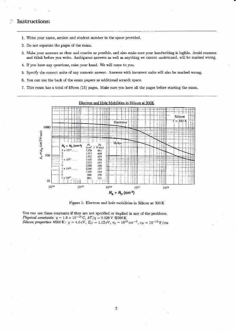
Electron and Hole Mobilities in Silicon at 300K .
1000~1)
"~,Q
Q.
::tC 100c:::t
10
1014 101.'i lolt. 1017
NA + No (cm-3)
101 R
Figure 1: Electron and hole mobilities in Silicon at 300 K
You can use these constants if they are not specified or implied in any of the problems.Physical constants: q = 1.6 X 1O-19C, kT/q = 0.026V@300KSilicon properties @300K: X = 4.0eV, Eo = 1.12eV, ni = 1010cm-3, fSi = 1O-12F/cm
2
r,-
Name: L 1M; ~t"Ntr J"ettN' DC Teacher: .§,... ~\.4i'no
Part I: (10 points)Given the bandgap energies of Ge, Si, and GaAs, indicate the order (using I-highest, 3-lowest; use same number if valuesare the same) of the semiconductors that satisfies the questions. Each question is independent the other. (2 pointseach)
Question I Ge GaAsSi
Band Gap Energy, Ea 3 2 1(given)
Electron-hole pairsat room temperature
1 2- 3
Resistivityat room temperature 3 of I
Each is doped with a donorconcentration of 1016 cm=". The , , \donor ionization energy is
0.06 eV. Which has highestelectron concentration at 300 K?
Each is doped with a donorconcentration of 1016 cm=". The
donor ionization energy is I l 30.06 eV. Which has highesthole concentration at 300 K?
Each is doped with a donorconcentration of 1016cm-3. As
\ L 3temperature is increased, whichwill become ''intrinsic'' (nssp)first? Use I-first, 2-second,
3-third
3
~
Name: PM, tW6IfN6 (f()*" y. DC Teacher: Q,"" 1tfvJl?()
Part II: (10 points) 4Five students were asked to determine the resistivity of a single semiconductor bar. Each of the students tried to applya voltage across the same sides of the sample (the voltages applied mayor may not be the same) and measured theresulting current. The students were provided with a supply that can provide any voltage they want, very small or. verylarge, and it is not current limited. Knowing the dimensions of the sample, the students assumed the resistivity to beequal to (Vapplied/lmeasured) x (Area/Length) from R = pL/A. However, the students were not able to come up withthe same resistivity values. The students' results are summarized below:
PI = P2 < P3 < P4 = P5
1. For some of the voltages applied, the produced current (current density) diverges from the usual case. Whatphenomenon is responsible for the differences in the "measured" resistivity? (2 points)
I !H'j'
2. Fill up the table with the relationship between the voltages applied and currents measured. Suppose the phenomenonstarts to take full effect only at V3. Use =, >, <, =/-, ? (if cannot be determined). No points will be given if theanswer in the previous question is incorrect. (4 points)
?
= t
~ 3. If originally, the semiconductor used was an N-type with ND = 5 x 1Q16cm-3 and it was perfectly compensated.With the temperature at 300K and using the table provided for carrier mobility, what is the resistivity of thecompensated semiconductor. Round your answers to three significant digits. (4 points)
_ .. ,~ 0.., ,I r- ,,,t'l .1 ,.. No ~.'ft ~, .."p1_>1II -:;1"".. +1Pfp n~'" ~ ,w (U<>' rob oe"'111 ... .> "It,v OWl rn... f'
..( \/, ~ h -:.331 OI'I'2-/v·(ttI.hlrr"t) { 'o"'Iee.J /\CD, tl" ....N.Ile) ~ I •
"0 JAn " fet ~ ''lv- #f-C,. "fl"~')(lo-ii Q/#VI t\.'lI\<p~", -"". ~".;.-ct« ...........
•~ ~~~~! ~- ...-" 'I~ K Sct" n--.:u '1.0. 11ft, ]l. -"'_ Q!'1!ot; ~ Ittrh'~duc~
IIlCU ~ ~fel?l'eo;teJ
4
•
1 DC 'Teachers d1r "1'"'"
Part III: (10 points)1. Determine the Arsenic doping concentration needed to move Ep by l.06eV from Ev at T=300K. ~urne- ~ .
fj..-fy· "oloeV, f,- e.. " ~-I'o('eV" -o·.elI_ ~f"- ~t ~,.~eNtr - ~t ,. ferill ( n1)
n.." nj; e(tF~tc)ltr " «. 8.tft1~'<fO" 7t1O'f ICftI.
2. Ifni = l(lT(3/2)e-EG/2kT where Ea may be assumed to be constant. with T, determine the doping concentrationNv in a Hi semiconductor such that the ratio n;/Nv = 1.5 at T = 55oK.
'l.. A; r 'I.. --r.14r II' ~~ "l - e, _, ~ - T~ t. ~ ... If, ~l/f'3'S'''''IO'$'" /(Krr$.~.'"
()t;:;;...,.t "-
,-I N_v_=_,_,_'~_s_r_x_/o_'O_~_C+»_i_ __J1 --t5
•
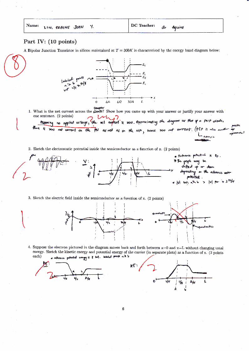
Part IV: (10 points)A Bipolar Junction Transistor in silicon maintained at T = 300K is characterized by the energy band diagram below:
C9 " "
Lc..: , I " ~ . - - _ Ej
',:,.. I.: I : EF
E,,,,
-f------f---t----t--+--- .r(J U4 U2 3U4 1.
l~
1. What is the net current across the~? Show how you came up with your' answer or justify your answer withone sentence. (2 points) l/v¥
flwanill lUI lit&' lIoltoCl(~ lid fit wrJ. RpffT1Ximah', rflJ.,_ =r: o.r ~ 'if 0. fNP di7J.,p_~-.:J Of'!' I.} I . r"f'l1<~ it ~ ~ CAIr1VIi <S'n ~ ;,; ttf well a,r O'n ~ AlP MnCl- urv ~ et#YtI?t-. (ptP fl ...{,D ~ .".
) L ..,I'~"'",loLtrl'h rl ''""
I!!iIst:r
2. Sketch the electrostatic potential inside the semiconductor as a function of x. (2 points)
3. Sketch the electric field inside the semiconductor as a function of x. (2 points)
\\
4. Suppose the electron pictured in the diagram moves back and forth between x=O and x=L without changing totalenergy. Sketch the kinetic energy and potential energy of the carrier (in separate plots) as a function of x. (2 points,,wX' '.~~ ""1l" ,.... ......,.. •• >, I<t, .< 'I .,~",;L; , I J.-!C2,: x..
tpt=:. ~ ~~ lLN \. o"'l--__'~~--;--+--r---1r---:+--1-/01 j 'It. I BIN l
0. J
6
I DC 'Teachert - "r"""
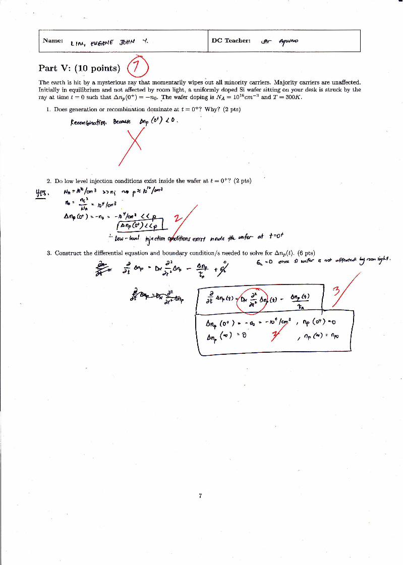
Part V: (10 points) 0The earth is hit by a mysterious ray that momentarily wipes out all minority carriers. Majority carriers are unaffected.Initially in equilibrium and not affected by room light, a uniformly doped Si wafer sitting on your desk is struck by theray at time t = 0 such that ~np(O+) = -no. ,The wafer doping is NA = 1Q16cm-3 and T = 300K.
1. Does generation or recombination dominate at t = O+? Why? (2 pts)
t«#WI"""",tl,.". ~ Dnr tot) '- 0 .
!2. Do low level injection conditions exist inside the wafer at t = O+? (2 pts)
IJfs . ~flt": /O"'/cm '3 ~')"i ~ r~ /0'"/~J, ilt l
:~:, :-::~~~'I<-'«~ Z.I b"p (0+) U,t Li. ltsw - ~ Pjtc/I'1lI ffrM./" e~l7f In(itk ~"../er- (),t t=ot
3. Construct the differential equation and boundary condition/s needed to solve for t..np(t). (6 pts);},._ d1 D ~ ~ 0 ",,,,,,,,"~ t¥XfV Il ..# ~. tJ ,_. ,1.:1.
~ ~ &!p ... f),.t - Llt!p 6n, of" d \.~ . ~t .Jta. t 7~
"
6rlt (0+ ) " - 00
hn (00) ,. 'Dr
II nf (o"t) "0
I Or ( ... ) :c "flO
7
._"'-"-------------------
I DC Teach";',
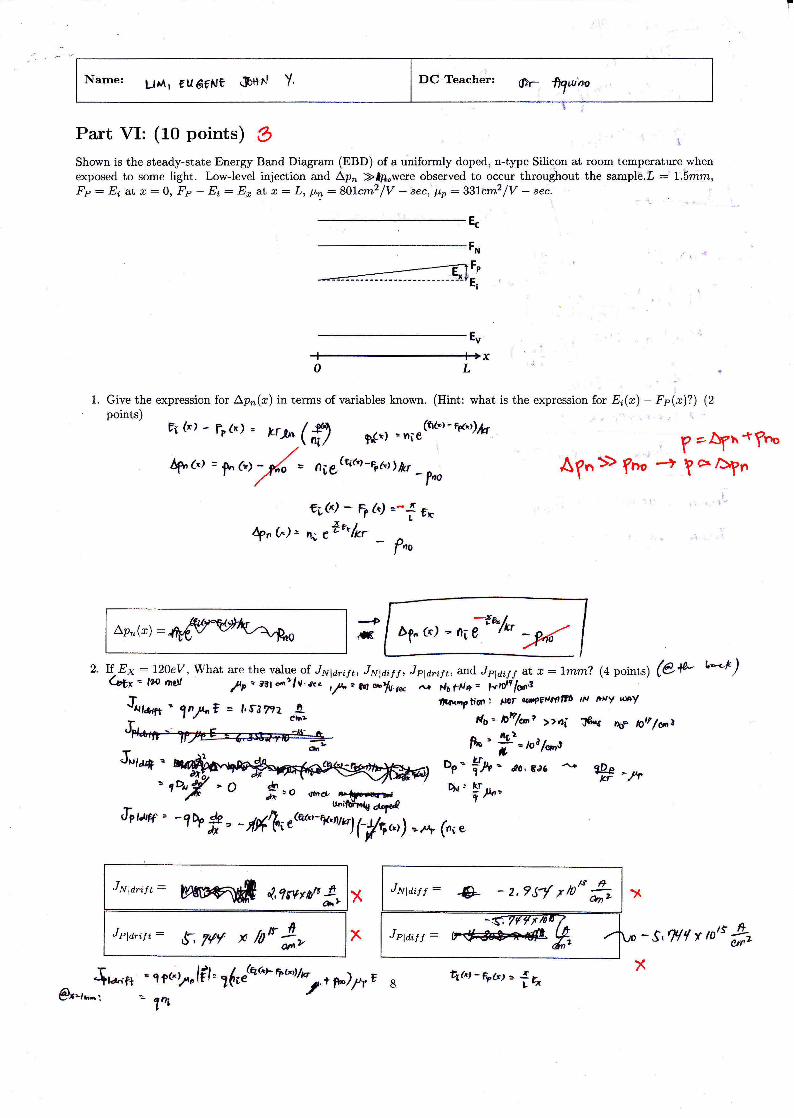
Part VI: (10 points) 8Shown is the steady-state Energy Band Diagram (EBD) of a uniformly doped, n-type Silicon at room temperature whenexposed to some light. Low-level injection and !:;.Pn »'nowere observed to occur throughout the sample.L =' 1.5mm,Fp = E, at x = 0, Fp - E, = Ex at x = L, j),r: = 801cm2 IV - sec, j),p = 331tm2 IV - sec.
------------------Ec
-------------------FN
~Fp---------------- -- 'E;
-------------------Ev
-r------------------++xo L
,1. Give the expression for !:;.Pn(x) in terms of variables known. (Hint: what is the expression for Ei(X) - Fp(x)?) (2
points) c
t'i (-,:)- f, ("It)" "f'- (~ (fll")-rpe:d)hr 1-.P'"if 'f>''') ""'ie
6f\,,()t) :: .an 6> - A~"e (1-.0 (ti<"-FpM)/tr,.. /0' ~v -PtlO
f ::;:..tJr)o; ~r~A fn ->"> fno _,. Y c=. ~r'\
,
r;"'Y;-. -r-~------------------__,
I N~, CIA" 1!<6t.,.,.- J'ltj/ 'f. I DC 'Teachert
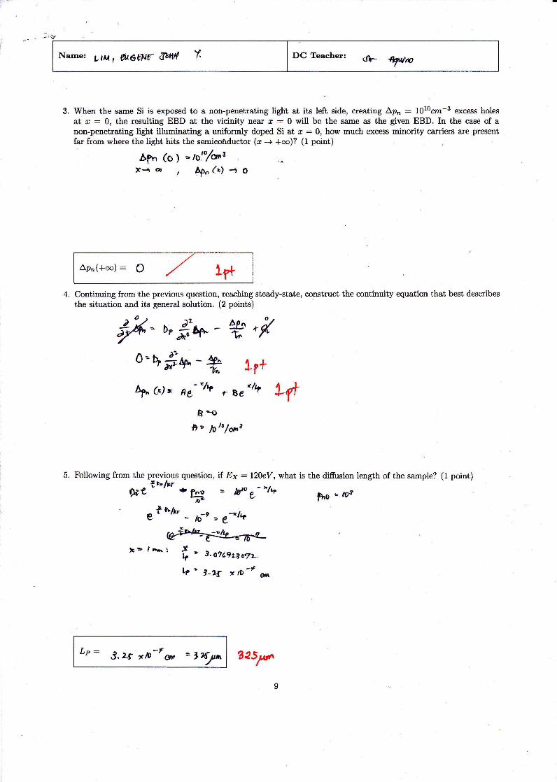
3. When the same Si is exposed to a non-penetrating light at its left side, creating D.pn = 1010cm-3 excess holesat x = 0, the resulting EBD at the vicinity near x = 0 will be the same as the given EBD. In the case of anon-penetrating light illuminating a uniformly doped Si at x = 0, how much excess minority carriers are presentfar from where the light hits the semiconductor (x -+ -l-co)? (1 point)
hrn (0) ~IQ!D!Clrt3X'-'I 00 hp() (~) ..., 0
D.Pn(+OO) = 0 -:4. Continuing from the previous question, reaching steady-state, construct the continuity equation that best describes
the situation and its general solution. (2 points)
1r+A... - ~/'_ 'J{/I-f'" (fJ)" lie ..,. r ae T
Q-oIt,. 10 10/ ()IfIl
5. Following from the previous question, if Ex = 120eV, what is the diffusion length of the sample? (1 point)tt .../~ _,.~-e ....~ "" ~ e, I"" h.n ,..«J3 .
/010 rrw.a t~/1tre' (' -~ -"'/1-
-10 ""e'"~
'Ii; ~ 3. 0'7'9~o?'2-
4> " ~. 23 :J( ID -~ ~
Lp=
9
•
DC Teacher:
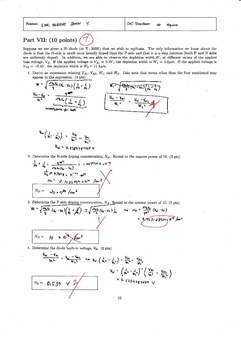
Part VII: (10 points) (J)Suppose we are given a Si diode (at T=300K) that we wish to replicate. The only information we know about thediode is that the N-side is much more heavily doped than the P-side and that it is a step junction (both P and N sidesare uniformly doped). In addition, we are able to observe the depletion width,W, at different values of the appliedbias voltage, VA. If the applied voltage is VAl = 0.3V, the depletion width is WI = 5.6fJ-m. If the applied voltage isVA2 = -O.4V, the depletion width is W2 = l1.1fJ-m.
1. Derive an expression relating VAl, VA2, WI, and W2. Take note that terms other than the four mentioned mayappear in the expression. (4 pts)
W" f!..~(V~i-VII)(~1t t Jo)t:t~
Vl.i - VitI
2. Determine the N-side doping concentration, ND. Round to the nearest power of 10. (2 pts)
t -t J _ ,w'- : t.a\\"'f'7b'l ~ >c/O-I'!
-;:r~ No - ,lSi. f,.-(v,,; _ \fit')..LND ~ If. 70'18- '" 10-2.1- C#/Iof1
u«> 02. 12 n. 'fO" YJ 1074
3. Determine the P-side doping concentration, NA. Round to the nearest power of 10. (2 pts)
W,. I~ llA,i-V,,)(i. tt) Z~/I ~ N~" ~~; (IIw-V.)Y .~.~.,</~,
rN-A--=--'-o--)--ro-~---~--3----~1
4. Determine the diode built-in voltage, Vbi. (2 pts)
Vb! - VII' -::. "lJi - \J,,"l."-'1')..- w.,.."-
10
--/'t>'!1 -,- --,
r~ame, ~IM,",6""" <To,"" DC Teacher:
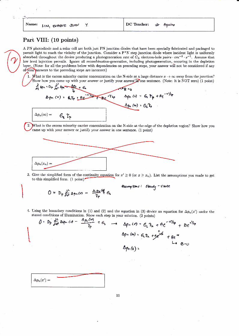
Part VIII: (10 points)A PN photodiode and a solar cell are both just PN junction diodes that have been specially fabricated and packaged to
Bpermit light to reach the vicinity of the junction. Consider a P+N step junction diode where incident light is uniformlyabsorbed throughout the device producing a photogeneration rate of GL electron-hole pairs· cm-3. s-l. Assume thatlow level injection prevails. Ignore all recombination-generation, including photogeneration, .occuring in the depletionlayer. (Note: for all the problems below with dependencies on preceding steps, your answer will not be considered if any
nswers to the preceding steps are incorrect)
hat is the excessminority carrier concentration on the N-side at a large distance x ---+ 00 away from the junction?ow how you came up with your answer or justify your answer' one sentence. (Note: it is NOT zero) (1 point)~ oJ!
~Pn(OO) =
r2:'what is the excess minority carrier concentration on the N-sid~at the edge of the depletion region? Showhow youVcame up with your answer or justify your answer in one sentence. (1 point)
3. Give the simplified form of the continuity eguation for x' ?:: 0 (or x ?:: z.,). List the assumptions you made to getto this simplified form. (1 point)- -.,
4. Using the boundary conditions in (1) and (2) and the equation in (3) device an equation for ~Pn(x') under thestated conditions of illumination. Show each step in your solution. (2 points)
O '" 1>.' ~ A,b (,JJ tJf,J":1 T G.P J-14" Of " '" _."
1'1'
\
__ ---:::::::0:==-~Pn(x') =
11
DC Teacher:
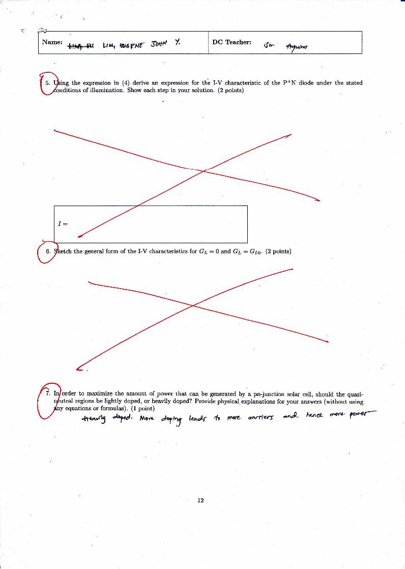
Ding the expression in (4) derive an expression for th~ I-V characteristic of the P+N diode under the stated~nditions of illumination. Show each step in your solution. (2 points)
1=
etch the general form of the I-V characteristics for GL = 0 and GL = GLO' (2 points)
(J0rderto maximize the amount of power that can be generated by a pn-junction solar cell, should the quasi-utral regions be lightly. doped, or heavily doped? Provide physicalexplanations for your answers (without usingy equations or formulas). (1 point)~ ~.~~I"~ 1- ~ aPVriu-s .,..,J_. 1v.¥I.~ (Mf't-- ~
12
I DC 'Teacher:
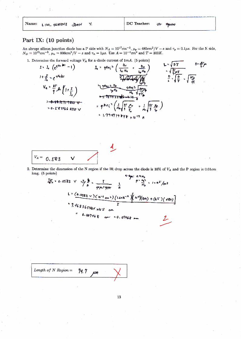
Part IX: (10 points)An abrupt silicon junction diode has a P side with N A = 1017em -3, J-Lp= 4S0cm2IV - sand 'Tp = O.IJ-Ls. For the N side,ND = 1015cm-3, J-Ln = SOOcm2IV - S and 'Tn = 1J-Ls. Use A = 1O-3cm2 and T = 300K.
VIt '> 1:.1 0_ ·r·· I)1'" u:k
v 212. Determine the dimension of the N region if the IR drop across the diode is 10% of VA and the P region is O.Olcm
long. (5 points)
.u<;,,. o.OS-83 V :>'1 ~ ~. r(+ '1ft,A.t1PJAr
l..A
~ 7. of, i~J'r-r,.., t~ Tf9f )C/o -.] a-
.:: d. 007'1" i" <I.-' ...o. 01",,_ _ Z-~
I Lenqtli of N Reqiori ~ 7'1. 7 r f{113
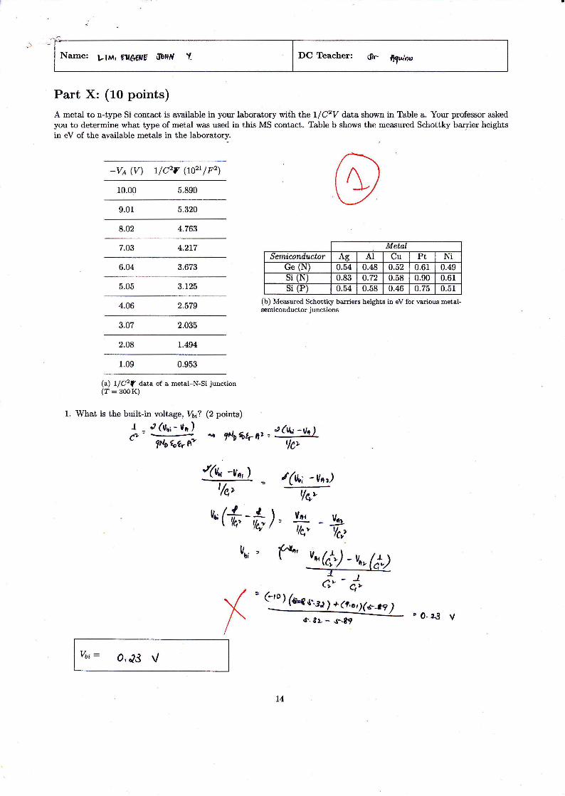
Part X: (10 points)A metal to n-type Si contact is available in your laboratory with the 1/02V data shown in Table a. Your professor askedyou to determine what type of metal was used in this MS contact. Table b shows the measured Schottky barrier heightsin eV of the available metals in the laboratory.
-VA (V) 1/02, (1021/P2)
10.00 5.890
9.01 5.320
8.02 4.763
7.03 4.217
6.04 3.673
5.05 3.125
4.06 2.579
3.07 2.035
2.08 1.494
1.09 0.953
MetalSemiconductor Ag Al eu Pt Ni
Ge (N) 0.54 0.48 0.52 0.61 0.49Si (N) 0.83 0.72 0.58 0.90 0.61Si (P) 0.54 0.58 0.46 0.75 0.51
(b) Measured Schottky barriers heights in eV for various metal-semiconductor junctions
(a) 1/C2f' data of a metal-N-Si junction(T = 300K)
1. What is the built-in voltage, Vbi? (2 points)1 oJ (libi - lilt )
C'l- = - - "'"1No fofr Pi""
V~(~ -1._)_~.. 'ICy" -
~
:;
Vbi = O,J3 V I14
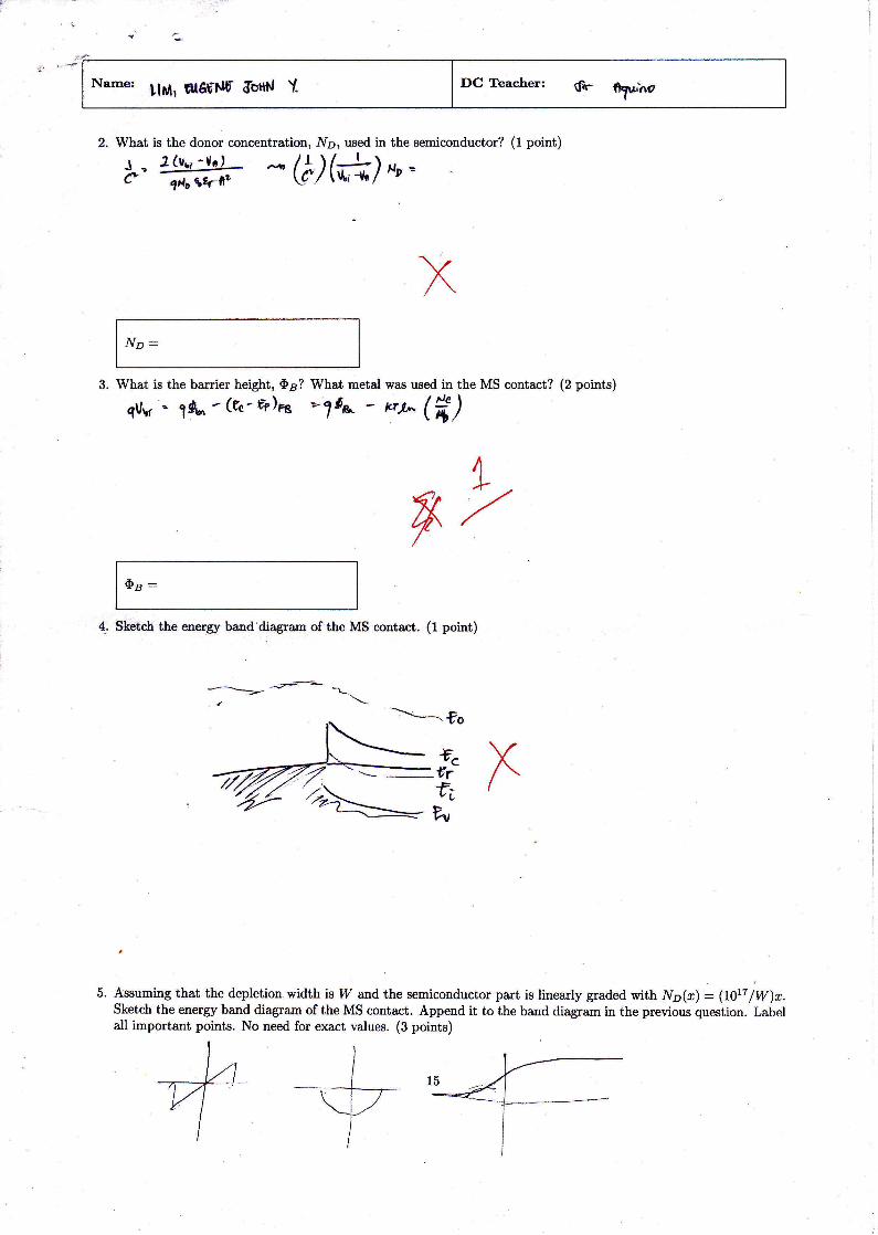
I\I
2. What is the donor concentration, ND, used in the semiconductor? (1 point)
j .,. l(v ..r~YIII) .....__,/1)(_L) J.Jp '"CO' ,Nil \Srft" \§' v-,i ->I,
x3. What is the barrier height, <I>B? What metal was used in the MS contact? (2 points)
qVItf ... ,~ ~ (ee - ep)F8 ~7~&.. - lap.. ('/;)
<I>B =
4~.Sketch the energy band diagram ofthe MS contact. (1 point)
~~-~" ~.po
w~t:~'f
5. Assuming that the depletion. width is W and the semiconductor part is linearly graded with ND(X) = (1017 jW)x.Sketch the energy band diagram of the MS contact. Append it to the band diagram in the previous question. Labelall important points. No need for exact values. (3 points)