eee225: analogue and digital electronics - lecture ii · opamp circuit dc conditions di erential...
TRANSCRIPT
EEE225: Analogue and Digital ElectronicsLecture II
James E. Green
Department of Electronic EngineeringUniversity of Sheffield
1/ 17
2/ 17
EEE225: Lecture 2
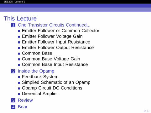
This Lecture1 One Transistor Circuits Continued...
Emitter Follower or Common CollectorEmitter Follower Voltage GainEmitter Follower Input ResistanceEmitter Follower Output ResistanceCommon BaseCommon Base Voltage GainCommon Base Input Resistance
2 Inside the OpampFeedback SystemSimplified Schematic of an OpampOpamp Circuit DC ConditionsDifferential Amplifier
3 Review
4 Bear

3/ 17
EEE225: Lecture 2
One Transistor Circuits Continued...
Emitter Follower or Common Collector
Emitter Follower / Common Collector
A kind of “voltage follower”or “buffer”
Approximately unity voltagegain
pnp or npn versions possible
High current gain
May be thought of asimpedance transformer (socan all transistor circuits...)
vs
RS
+Vs
RE vo
−VSIn this figure the biasing circuitry is contained as an effectiveresistance within RS

4/ 17
EEE225: Lecture 2
One Transistor Circuits Continued...
Emitter Follower Voltage Gain
vs
RS
ib
rbevbegm vbeor β ib
ie
REvo
ve
vb
vo = vbe RE
(1
rbe+ gm
)(1)
≈ vbe RE gm (2)
and a relation between vbe , vsand vo is given by summingvoltages around the input loop.
vs = ib RS + vbe + vo (3)
= vbe
(1 +
RS
rbe
)+ vo (4)
using the result in (2) toeliminate vbe ,
vovs
=rbe gm RE
rbe gm RE + RS + rbe(5)
=RE
1gm
+ RSβ + RE
(6)
1 The gain is non-inverting
2 Gain ≈ 1 if RE >> RS/βand RE >> 1/gm

5/ 17
EEE225: Lecture 2
One Transistor Circuits Continued...
Emitter Follower Input Resistance
The input resistance is given byconsidering vb/ib, recall (1)
ve = vbe RE
(1
rbe+ gm
)(7)
and summing up the voltages...
vb = vbe + ve (8)
= vbe + vbe RE
(1
rbe+ gm
)(9)
= vbe
(1 + RE
(1
rbe+ gm
))(10)
since vbe = ib rbe and gm rbe = βwe can write,
ri =vbib
= rbe +(β + 1) RE (11)
Generally (β + 1)RE >> rbe sothe input resistance is dominatedby the (β + 1)RE term. Bycomparing this result with theinput resistance of thenon-degenerated commonemitter amplifier we could shownegative feedback can be used toincrease the input resistance of atransistor stage.

6/ 17
EEE225: Lecture 2
One Transistor Circuits Continued...
Emitter Follower Output Resistance
To obtain the output resistanceinject a test current it with theinput grounded and find vo/it .Summing currents at ve
(1 + β) ib + it =veRE
(12)
and summing up the voltages inthe base loop
ve = −ib (RS + rbe) (13)
substituting (13) into (12) andsolving for ve/it ,
ro =1
1+βRS+rbe
+1
RE(14)
RS
ib
rbevbegm vbeor β ib
ie
RE
ve
vb
it
ro ≈1
gm+
RS
β(15)
If β >> 1, the first termbecomes RS+rbe
β and if RE is
large, we can ignore the 1RE
term.

7/ 17
EEE225: Lecture 2
One Transistor Circuits Continued...
Common Base
Common Base Connection
Generally used in conjunctionwith other transistors in“circuit blocks”, butsometimes alone1. ie is theinput current (flowing fromvs), since ie = io + ib thecurrent gain (io/ie) is slightlyless than 1 (actually it’s = α).
vs
IE
RS RL
+VSIC
-VS
IBvo summing currents,
ie + ib + gm vbe = 0 (16)
1http://dx.doi.org/10.1088/0957-0233/23/12/125901

8/ 17
EEE225: Lecture 2
One Transistor Circuits Continued...
Common Base Voltage Gain
vs − veRS
+vberbe
+gm vbe = 0 (17)
ve + vbe = 0 so ve = −vbetherefore (17) can be solved forvbe
vbe = − vs
RS
(1RS
+ 1rbe
+ gm)(18)
≈ − vs1 + gm RS
(19)
approximation is because1/rbe = gm/β and β >> 1
At the output,
vo = io RL = −gm vbe RL (20)
combining this with (19) toeliminate vbe
vovs
=gm RL
1 + gm RS=
RL
re + RS(21)
where re = 1/gm.
The gain is non-inverting
Gain ∝ RL
If RS >> re gain controlledby ratio RL/RS

9/ 17
EEE225: Lecture 2
One Transistor Circuits Continued...
Common Base Input Resistance
Common Base Input Resistance
The resistance looking into theemitter,
ri =veie
=ve
−vberbe− gm vbe
(22)
Since ve = −vbe andgm >> 1/rbe this reduces tori ≈ 1
gm= re The value is small
10s - 100s Ω
There is another model of the transistor called “T Model” in whichre plays a much bigger role. However hybid-π is the only model wewill use. The original π paper is by Giacolletto2.
2http://dx.doi.org/10.1109/JSSC.1969.1049963

10/ 17
EEE225: Lecture 2
Inside the Opamp
Feedback System
Feedback Systems (Quick reminder)In EEE118 we discussed the opamp in terms of a general feedbacksystem.
vi +–
H voH
(vi −H vo)G vo
So vo = G (vi − H vo) (23)
or vo (1 + G H) = G vi (24)
vovi
=G
1 + G H(25)
If |G H| >> 1,
vovi
=G
G H=
1
H(26)
System dependent on H, designer controls H with ratio of resistors.

11/ 17
EEE225: Lecture 2
Inside the Opamp
Simplified Schematic of an Opamp
Q1 Q2
RE
IE
R1
Q3
RVA
IC3
Q4
VA Q5
RL
v+
v−
– VS
+ VS
Input stagesubtracts inputs
Voltageamplifierstage
Ouput Stageallows power gain
v+
+–
v−
G O/P
vi
vo1
va
vo4
IC1 IC2
Input stage: differentialamplifier or “long tailedpair”. Subtracts the inputs.
Voltage amplifier stage(VAS): common emitteramplifier. Provides majorityof voltage gain.
Output stage: emitterfollower. Increases currentcapability of VAS (voltage ×current = power... hence“power gain”.

12/ 17
EEE225: Lecture 2
Inside the Opamp
Opamp Circuit DC Conditions
Opamp will not work properly without feedback. Feedbackcontrols the gain of the circuit but also helps define the DCconditions. Feedback adjusts vi in order to achieve theinternal voltage drops required for proper operation. If vo =0, vi will be at the value it needs to be in order to make vo =0. Feedback is not shown on prior slide.
If v+ ≈ v− ≈ 0, VE1 and VE2 ≈ 0.7 so IE ≈ (+VS − 0.7)/RE .
IE splits between Q1 and Q2 to form IC1 and IC2.
IC1 has two functions 1) create a voltage drop of 0.7 V acrossR1 in order to bias Q3 into conduction. 2) Provide the basecurrent for Q3. IC1 will be 0.7/R1 + IC3/hFE3.
The value of IC3 varies with VA and hence with Vo4 butassuming VA = 0, IC3 = +VS/RVA.
IC2 is returned directly to the negative supply.
In the case where v+ ≈ v− 6= 0, there is a common modeinput voltage, vcm, and IE ≈ (+VS − vcm)/RE .

13/ 17
EEE225: Lecture 2
Inside the Opamp
Differential Amplifier
RE
I
+VS
Q1 Q2
V +i +∆V
I2 −∆I
R1
V −i −∆V
I2 +∆I
vo = −∆I R1
-VS
Vo = I2 −∆I R1
If v+ increases by ∆vi andv− decreases by ∆vi , theaverage of v+ and v− isunchanged so IE isunchanged because Vbe isunchanged.
If v+ and v− increase ordecrease by ∆vi , vi is calleda “common mode signal”ideally the differentialamplifier will not amplifyany common modecomponent of the input.

14/ 17
EEE225: Lecture 2
Inside the Opamp
Differential Amplifier
RE
I
+VS
Q1 Q2v+
IC1
R1
IC2
Q3
+0.7 V
vo1
−VS
We must consider the effects ofthree transistors. Q1 and Q2 arethe input differential pair.
Q3 must also be considered nowbecause its input resistance formspart of Q1’s collector loadresistance. If the input signal isregarded as v+ with respect toground, Q2 looks like a commonbase connection and can berepresented by its common baseinput resistance 1/gm2. Thecollector current of Q1 sees tworesistors in parallel, R1 and theinput resistance of Q3. Q3 is acommon emitter amplifierwithout degeneration. Its inputresistance is rbe3.

15/ 17
EEE225: Lecture 2
Inside the Opamp
Differential Amplifier
vi
rbe1 vbegm1 vbe1or β1 ib1
RE ve1 re2 R1 vo1 rbe3
i1
ib1
ie1
A small signal equivalent circuitdescribes the three transistor circuitblock according to our simplifications.
This small signal model isvery similar to thecommon emitter withdegeneration from Lecture1. In this case RS = 0 andRE and RL are parallelcombinations RE//re2 andR1//rbe3. SinceRE >> re2, re2 dominates.The gain expression forthe circuit is (based on thedegenerated CE analysis)
vo1
vi= −R1//rbe3
re1 + re2(27)

16/ 17
EEE225: Lecture 2
Review
Review
Considered the emitter follower circuit (voltage gain, currentgain, input and output resistances).
Considered the common base circuit (voltage gain, currentgain, input resistance).
Recapped the idea of the opamp as a feedback system.
Introduced a simplified schematic of an opamp.
Developed some ideas around the DC conditions of thesimplified opamp
Looked at the combination of three transistors into adifferential amplifier + common emitter stage and consideredtheir combined effect.

17/ 17
EEE225: Lecture 2
Bear