eeg/emg using dry electrodes -...
TRANSCRIPT
EEG/EMG Using Dry Electrodes
Nick Arango
5/14/2015
1 Introduction
This paper presents a EEG/EMG measurement device designed for applications in computerinterface and sleep monitoring. This device attaches to the users scalp and face using dry,bed of blunt needle, probes which is more convenient for users and posed interesting designchallenges. The final device was able to recognize blinking of a user’s eyes through EMGsignals, provide data to a computer about the direction of a user’s eyes through EMG signals,and measure EEG signals to some degree. Testing was a challenge due to the small voltagelevels of EEG and EMG signals. Using the device to measure Electrocardiograms (ECGs)proved to be a simple way of validating correct operation before measuring the smaller EEGand EMG signals.
1.1 Motivation
Measurement of microvolt scale signals on the skull correlated with brain activity can pro-vide useful data for doctors diagnosing sleep or brain disorders. Similar signals generatedby the motion of the eyes is similarly useful. The cost of electroencephalograms (EEGs)used to measure brainwaves and electromyograms (EMGs) have decreased dramatically andconsumer products promising in home sleep monitoring. Even simple mind control toys havecome to market.
These products amplify the small EEG/EMG signals, digitize these signals, and performsimple digital filtering to extract signals correlated with different thought patterns, sleepcycles, eye movement or blinking.
The signal processing needed to analyze sleep, concentration or eye movements is rela-tively simple. In the case of EEG, the measured signal is split into several frequency rangeseach correlated with different brain activity. The relative magnitudes of the frequency rangesindicate the type of brain activity. Due to the low frequency of the signals involved thesesignals can be computed by low power microcontrollers or analog electronics.
There are two standard ways of electrically connecting EEG/EMG circuitry to a user’shead that each provide different strengths. Passive wet electrodes use a conductive gel toprovide an electrical connection to a user. These electrodes can not contact skin throughhair and are either non-reusable or require cleaning after each use. They do provide anadvantage of low output impedance reducing noise in the system. Dry active electrodes canmake contact through hair and don’t require cleaning. However, their output resistance
1
ActiveElectrode Differential
Differential Mode Signal Optical ComputerAmplification Isolation Audio Jack
ActiveElectrode
DRL Feature LEDDriver Detection Indicator
Common ModeSignal
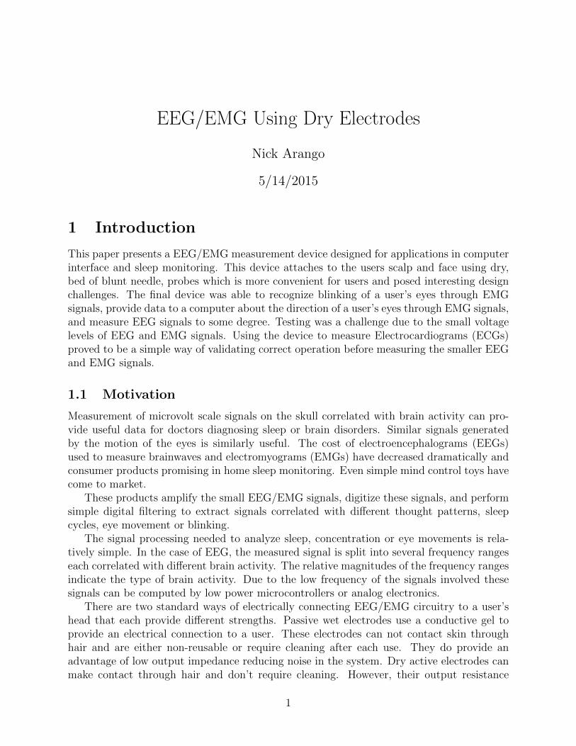
Figure 1: High level block diagram of the portable low noise EEG/EMG. Active electrodesconnect to the scalp and face of the user and the output attaches the the laptop of the user.An LED indicates when the user blinks.
is rather high and need additional circuitry to reduce noise. In consumer applications dryactive electrodes are their obvious choice due to the lower maintenance at the cost of increasedcircuit complexity.
1.2 Changing Scope and Goals
This project initially aimed to create a portable electroencephalogram (EEG) for use as acomputer interface device with low setup and cleanup time. To achieve this goal we builtactive dry electrodes, filtered differential amplification, analog optical isolation and analysiscircuitry. As the device was tested it became clear that EEG data was not sufficiently reliableboth due to the circuit and due to the nature of EEG so EMG signals of the eye becamethe demoing benchmark. These signals were still on the order of 50uV so the design of theamplifier was similarly challenging, just simpler to test.
2 Design
2.1 System Overview
The body potential measurement device, at a high level, has four major components: dryactive probes, low-noise high-gain differential amplification, analog signal processing, andanalog optical isolation. A system diagram is shown in figure 1.
The dry electrodes connect to the circuit to the user and require active buffering oramplification to drive the long signal wires with a low output impedance. The low impedancereduces electromagnetic interference.
The differential amplifier end takes small signals from dry electrodes attached to thescalp and amplifies the microvolt level signals at the frequencies 1 and 40 Hz that arecorrelated with brain activity and muscle contraction. Because the sensed signals are sosmall, immunity from outside noise sources and reduction of noise from electrical components
2
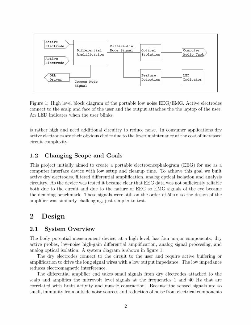
Figure 2: Headers used in the dry electrode
is critical. Fortunately the main component of interference, 60 Hz mains hum, is outsideof the relevant frequency range for EEG and EMG and therefore is filtered out. The othermajor sources of noise are ripple on the power supply, RF interference on high impedancesignals and component drift.
Because the EEG signal is inherently differential, once buffered, the electrode signals willbe subtracted in a differential amplification stage. The common mode signals will providean additional noise source and while this is mitigated by the common mode rejection ratioof the amplifiers, further action can be taken. To reduce this source of noise, the body isdriven to a potential to cancel out the common mode voltage of the electrodes. The commonmode signal was be low passed before driving the body to prevent instability.
The design of this circuit posed challenging due to the low noise requirements. Testingalso presented a set of challenges. Bench function generators don’t provide the microvoltlevel signals needed to test the electrode buffers and differential amplifier. However, simpleresistor attenuators can provide the necessary signals at reasonable common modes. Eachof the amplifiers were tested individually prior to integration in the front end by measuringthe frequency response given microvolt inputs.
2.2 Characterization of Dry Electrode
Characterization of the connection between the dry electrodes and a user’s skin was impor-tant in designing the low noise active probe amplifiers. An LRC meter was used to measurethe contact resistance of the needle electrodes over a range of frequencies. For a baseline,wet electrodes were attached to the forearm 6 inches apart and the LRC meter was used tomeasure the sum of the two contact resistances plus the resistance of the skin. One of thewet electrodes was removed and replaced with a dry electrode and the experiment was runagain. The readings were compared to determine how much worse the dry electrodes wereas compared to the wet electrodes. Table 1 summarizes these results. Frequencies between 5and 100 Hz were tested. The lower limit was a limitation of the LRC meter and all relevantmeasured signals would be well below the upper tested limit. Note that the resistance ofhuman skin at a distance of 6 inches is on the order of kilaohms.
3

Frequency (Hz) 5 7.5 10 15 25 35 45 55 65 75 85 95 100Wet Resistance (MOhm) .24 .16 .13 .12 .09 .07 .05 .05 .04 .04 .04 .04 .03Dry Resistance (MOhm) .52 .45 .43 .41 .39 .39 .39 .37 .37 .37 .37 .36 .36
Table 1: Wet and dry electrode resistance resistance as a fucntion of frequency
The contact resistance of the dry electrode was not just a function of frequency but alsoa hysteretic function of pressure. If the needles very lightly touched skin, a reading of 10’sof mega Ohms was measured. There was some critical pressure after which the resistancewas characterized by the transfer data in table 1. If the probes was removed and replacedor translated the resistance would increase to 10’s of mega Ohms again.
This is most likely due to the pressure of the electrodes on the skin piercing throughthe Stratum Corneum composed of dead skin and touching the living Stratum Spinosum, amore conductive, living layer of skin cells. This gave insight on how to place electrodes on ausers body for both comfort (minimizing pressure) and optimal sensing (minimizing contactresistance).
2.3 Active Probes
The design of the active probe circuit depended on the electrical characteristics of the dryelectrodes. Because of the high source impedance of the electrodes, the amplification circuithad to be physically very close to the electrode. By minimizing the length of wire between theelectrode and the amplifier, common mode interference was reduced. The physical proximitysuggested that the circuit needed to be small and therefore simple. To prevent interferenceon long power supply wires each amplifier was powered by a small battery necessitating theuse of low power components. Additionally, the high gain in subsequent stages of the circuitrequired a low output bias from the active probes. Bias of less than a millivolt was necessaryto prevent clipping in further stages. A simple non-inverting amplifier was implemented andthough the circuit is simple, great care was taken in the selection of the amplifier to meetthe specification. A schematic of the active probe is shown in figure 3a. The gain of twowas selected to ensure the correct operation of subsequent stages of the circuit. With toomuch gain, the DC bias becomes unmanageable for future stages. The feedback capacitorwas added to reduce high frequency gain to unity. Because the input stage was noninverting,reducing high frequencies below unity gain was not possible while maintaining high inputimpedance. The pin labeled S is an active low shutdown pin with an internal pullup to turnoff the amplifier and reduce power. In this application this pin was left floating. The twodominant sources of noise from the circuit itself are input offset voltage noise and input offsetcurrent noise. The power spectral density (PSD) of both of these noise sources behave like asingle pole at zero and a zero at some higher frequency. The frequency range relevant of theinput signals of this circuit ends well before the zero in the noise PSD and therefore mustcontend with the large low frequency noise refered to as 1/f noise. In selecting an opampfor this application, first input offset voltage and input offset current were considered. OnlyJFET or CMOS input stage amplifiers were considered due to their high input impedanceand any amplifier with an offset voltage greater than 500mV was rejected. This rejectedthe jellybean LM356 JFET input opamp with its 5mV offset. While this component has
4

Rfb
1k
rg
1k
U1
LT6010
Cfb
47n
C1
1n+V
V-
vout
Dry Electrode
(a) Active probe schematic (b) Input referenced noise spectral density
Figure 3: The active probe was designed to maximize input impedance, minimize outputoffset voltage, and minimize noise.
external trimming capability, re-tuning a potentiometer josteled through use did not seemlike a viable option. Then the input offset voltage and current specifications were considered.Because the source impedance was on the order of 300kOhms (as determined in the previoussection) current mode noise could be ignored if RMS current noise × 300kOhms is very muchless than the voltage mode noise. Unfortunately this was not the case for any of the practicalopamps. After LTSpice noise simulation of many amplifiers, the LT6010 was selected eventhough its RMS current noise was larger than other components. If the source resistance ofthe electrode was twice as large the LT6014 would have been selected as it has higher voltagenoise but lower current noise. A PSD of the amplifier noise is shown if figure 3b. The RMSnoise between the frequency of .1Hz and 50Hz is 3.1µVolts
The noise performance and fidelity of the LM6010 was verified by configuring the opampas a non inverting amplifier with a gain of 1000 and driving it with 10uV 1kHz sine wavegenerated by dividing a 10mV sine wave with a voltage divider in addition to measuring itszero input response. The low frequency noise was very visible in slow shifts of the offsetof the 1kHz output. The RMS of this noise was estimated at 2mV RMS between 0Hz and50Hz referenced to the output and therefore 2µVolts referenced to the input, validating thespecification of the device.
This component has advantages in power consumption. During normal operating condi-tions, simulation suggests a power consumption on the order of 70µ watts. This is result isbacked up by imperial observation. The active probes were constructed on two small bread-boards individually powered by nine volt batteries. A picture is shown in figure ?? Thesewere left on continuously for the two weeks after their construction and the voltage of thebatteries fell by less than 5mV in that time. Theoretically, one 9V battery could power anactive probe for 8.7 years, well longer than the shelf life of the battery.
The image shown has one component missing: the audio jack that connects the activeprobe to the subsequent stages. An audio jack was a convenient cable because of its flexibility,plug ability, and they have three conductors. One conductor was used as ground, anotherwas for virtual ground, and the third for signal. The other end of the audio cable connectedto the subsequent differential amplification stage.
5

Figure 4: Image of one active probe showing the dry electrode, LM6010, and 9 volt powersource
The image also shows significant room for improvement in the layout of the active probeto buffet noise immunity. A short orange wire soldered directly to the solder bridge thatconnects the pins connects the LT6010 through a breadboard row to the probe. Neither theneedles nor the high source impedance wires connected to the needles are shielded. If thiscircuit were laid out on a PCB, a virtual ground plane would shield
2.4 Differential Amplification
Differential amplification is accomplished with an instrumentation amplifier and circuitryto reject noise and DC offset. The common mode signal is also calculated by the circuit.This subsystem, in addition to all subsequent subsystems, is powered from a third ninevolt battery. A virtual ground is generated using a rail splitting voltage divider and anon-inverting buffer. A complete schematic is show in in figure 5
The AD610 instrumentation amplifier was used to subtract the signal from the twoprobes. Its 120dB common mode rejection ratio, high power supply rejection ratio, andlow input offset voltage make it an ideal part for this application. The 50uV input offsetvoltage permits the use of large gains. A gain of approximately 50 was used in this appli-cation and was set with a 1kOhm gain resistor. This was implemented with two series 510ohm resistors which allowed for the measurement of the common mode signal. To preventloading on that gain resistor center tap, the common mode signal was buffered with a rail torail opamp. Rail to rail operation is important here because the common mode signal mayvary widely and this signal is used in the right leg drive circuit to compensate for commonmode offset.
Two Sallen Key lowpass filters both with a gain of 10 amplify the differential signal while
6
U1
LT1168R1 510R2510
U2
LT1678
U4
LT1678
R3
1Meg
C1
1µF
R4
330k
R5
330k
C2
1µU3
LT1678
R610k
R7
100k
R8
330k
C3
1µU5
LT1678
R910k
R10
100k
C4
1µC5
1µ
R11
330k
C6
1µ R121Meg
U6
LT1678
R13
100kR1410k
Probe1
Probe2
-vV+
V+-V
VCOMMON
V+-V
V+-V
V+-V
V-+V
OUTPUT
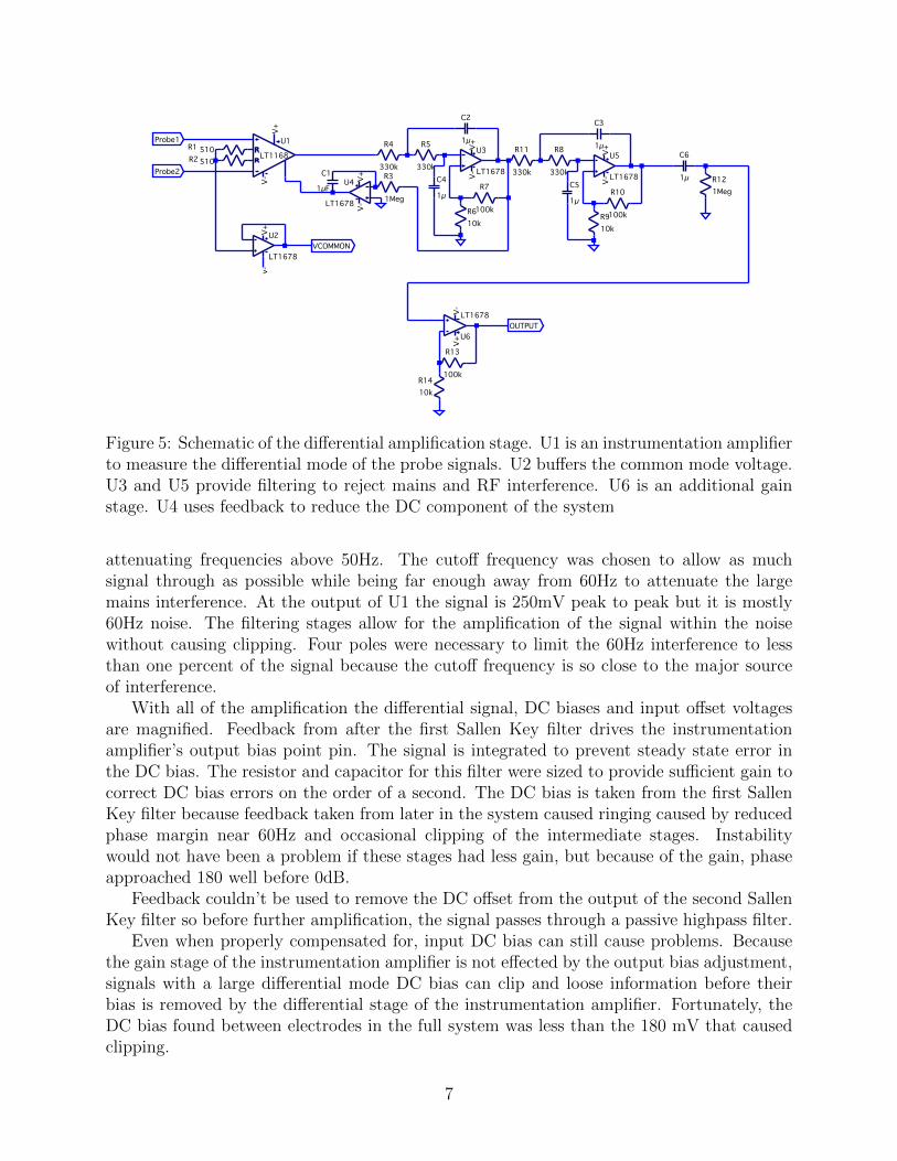
Figure 5: Schematic of the differential amplification stage. U1 is an instrumentation amplifierto measure the differential mode of the probe signals. U2 buffers the common mode voltage.U3 and U5 provide filtering to reject mains and RF interference. U6 is an additional gainstage. U4 uses feedback to reduce the DC component of the system
attenuating frequencies above 50Hz. The cutoff frequency was chosen to allow as muchsignal through as possible while being far enough away from 60Hz to attenuate the largemains interference. At the output of U1 the signal is 250mV peak to peak but it is mostly60Hz noise. The filtering stages allow for the amplification of the signal within the noisewithout causing clipping. Four poles were necessary to limit the 60Hz interference to lessthan one percent of the signal because the cutoff frequency is so close to the major sourceof interference.
With all of the amplification the differential signal, DC biases and input offset voltagesare magnified. Feedback from after the first Sallen Key filter drives the instrumentationamplifier’s output bias point pin. The signal is integrated to prevent steady state error inthe DC bias. The resistor and capacitor for this filter were sized to provide sufficient gain tocorrect DC bias errors on the order of a second. The DC bias is taken from the first SallenKey filter because feedback taken from later in the system caused ringing caused by reducedphase margin near 60Hz and occasional clipping of the intermediate stages. Instabilitywould not have been a problem if these stages had less gain, but because of the gain, phaseapproached 180 well before 0dB.
Feedback couldn’t be used to remove the DC offset from the output of the second SallenKey filter so before further amplification, the signal passes through a passive highpass filter.
Even when properly compensated for, input DC bias can still cause problems. Becausethe gain stage of the instrumentation amplifier is not effected by the output bias adjustment,signals with a large differential mode DC bias can clip and loose information before theirbias is removed by the differential stage of the instrumentation amplifier. Fortunately, theDC bias found between electrodes in the full system was less than the 180 mV that causedclipping.
7

U1
LT1678
R1
110k
C1
1µF
R2
330K
V+-V
VCOMMON RLD
Figure 6: Schematic of the right leg driver circuit
2.5 Right Leg Drive
The right leg drive (RLD) circuit set the user’s common mode voltage to increase the effectivecommon mode rejection ratio of the circuit. The name right leg drive is a holdover fromECG technology where the right leg is driven to a known potential to avoid interfering withthe operation of the heart. In this application the right leg drive was connected to the centerof a user’s forehead using a wet adhesive electrode.
The RLD circuit simply low-passes the common mode voltage measured by the differentialamplification stage. This amplification stage had a gain of 3 and a frequency cutoff ofapproximately half a hertz. The system was tested with higher gains and lower cutofffrequencies to improve the common mode rejection ratio but this lead to instability. Ideally,the passband of the RLD circuit would include 60Hz to reject the main source of commonmode noise. Unfortunately the reactance of the body at that frequency caused phase shiftsand significantly reduced open loop phase margin resulting in oscillation. A cleverer analysisof skin impedance might have provided insight into the construction of a lead network tocompensate for the user’s skin to provide more gain at 60Hz. Time constraints did notpermit that rigor of analysis.
The DRL was set to a higher voltage than the common mode measured by the instru-mentation amplifier. This was most likely due to the increased resistance of the wet adhesiveprobe at DC. In an attempt to avoid steady state error, the circuit was modified to act asan integrator by removing the feedback resistor and increasing the input resistor. The useof an integrator as a DRL output drove the system unstable. The exact mechanism for theinstability is not understood.
2.6 Feature Detection
When the active probes are connected the the user to measure EMG signals, eyes movementsand blinks are easily observable in the EMG signal on the oscilloscope. For example electrodeplacement was configured measure blinks, a 200mV 4ms pulse with a sharp leading edge anda gradual lagging edge is apparent on the EMG signal. Where the electrodes were placed toacheive this measurement is described in section 2.8
While the previous stage performed well in blocking the DC component of the signal
8

U1
LT1678
C1
1µ
R1
1Meg
U2
Comp
R2R
R3
R
R41k
R5
1k
Q1NPN
R610k
555_ALL
Gnd
Trig
Out
Rst Ctrl
Thres
Disc
Vcc R757k
C2
1µ
R8560
D1
D
-VV+
NI_GME
V+-V
V+
-VV+
V-
V+
-V
V+
-V
Tunable Potentiometer
Figure 7: Schematic of the blink detection circuit. A differentator generates a pulse on theedges of blinks and a comparator thresholds that signal to generate a pulse on blinks. A2n3904 is used as an inverter to generate an active low trigger signal for the 555 timer whichflashes the LED for a visible duration for each blink.
associated with the positioning of the electrodes, small variations in the pressure of theelectrodes on a user’s skin caused small, temporary changes in the DC offset of the EMGsignal. The noise associated with electrode pressure could not entirely filtered out becauseit occurs in the frequency range of interest. Thresholding the EMG signal directly to detectblinks caused spurious readings due to the wandering offset whenever the user moved theprobes. Because of the sharp rising edge of the signal, the derivative of the EMG readingprovided a clean way to detect blinks.
This signal was thresholded using the LM1011 comparator. The duration of the comparedsignal is was short and while it was visible on the oscilloscope, that did not provide acompelling demonstration. A 555 timer was configured as a monostable oscillator to pulseand drive an LED whenever the user blinked. The compared signal was inverted with acommon emitter amplifier to generate the active low trigger for the timer IC.
Setting the threshold of the comparator required some skill. Two hands were needed tohold the electrodes to the users face and a third was needed to adjust the potetiometer settingthe reference voltage. Imaginably, this was quite tricky for a single person to manage. Ideallythis threshold could have instead been calibrated dynamically by estimating the peak to peakvoltage when the user was not blinking, adding cushion room and storing that voltage in asample and hold. Unfortunately, there was not enough time to complete the construction ofthat circuit.
2.7 Analog Isolation
Optical isolation between the EEG/EMG and a recording device allows enables the use ofmains powered recording equipment without sacrificing signal quality. Referencing the high
9

(a) Isolation schematic. (b) Voltage transfer function
Figure 8: The analog optoisolation circuit provides 5kV voltage isolation between theEEG/EMG and the recording device while providing high lineary through much of the powersupply range. THe green trace shows the output where the blue trace shows the input
gain amplifiers to earth ground can introduce large common mode voltages (at DC andat 60Hz) to the input of the differential amplifier. To reduce the effect of this noise, theEEG/EMG circuit is battery powered and electrically isolated from wall.
Most isolation techniques are aimed at digital signals. The usual approach for passing ananalog signal across an isolation barrier is to first digitize it with with an analog to digitalconverter and then pass the signal over the isolation barrier either galvanically or optically.Both optical isolators and non integrated galvanic isolators have poor linearity to isolate ananalog signal without resorting to digital techniques feedback was necessary. A circuit togalvanically isolate analog signals is similar to an isolating DC/DC regulator with the outputvoltage set equal to the input signal. Integrated solutions exist but a discrete design wouldbe large, complicated, and introduce high frequency power supply ripple. Optical isolationFigure ?? shows the schematic of the circuit that enables the isolation.
This circuit uses the HCNR200 linear analog optocoupler from Avago Technologies thatcontains a single LED and a pair of photodiodes with matched optical characteristics. Onephotodiode lies on the driving side of the isolation barrier and the other lies on the receivingside. Transimpedance feedback is used to to set the current through the drive side photodiodeand because the two diodes are matched, also the current in the receive side diode. By sensingthe current through the receive photodiode with a transimpedance amplifier with the samefeedback resistor as the drive side, the output voltage is equal to the input voltage. Thefeedback resistor is selected to provide sufficient gain to overcome the nonlinearities of LED-photodiode system. One Mega Ohm was sufficient to provide a high degree of linearity. TheLED drive resistor is selected to prevent over-current if the full power supply were appliedover the LED and resistor in series. The one nanofarad capacitors reduce high frequencygain to maintain stability. The LED-photodiode system acts as a lag network so the systemwould be unstable without this compensation.
Deviation from of the output from the input in the spice simulation in figure 8b is dueto the limitations of the opamps. If the opamps operated rail to rail, the region of linearitywould continue further.
10

Figure 9: Placement of electrodes to make different measurements. A-B provides EEG. C-Emeasures blinking and virtical eye movement. D-F measures left-right eye movement. Drivenright leg(DRL) is driven from the circuit sets the common mode voltage
2.8 Electrode Placement
Electrodes could be placed in various positions on the face and scalp to measure differentbody potentials. Figure ?? shows a face and the positions of electrodes to measure differentfeatures. The designed in this paper was able to conclusively measure blinks with electrodesplaced on top an bottom of one eye and the motion of the eye to the left and right when theelectrodes were placed at the temples. The DRL was adhered to the center of the foreheadto minimize the DC bias between two electrodes.
Through experiments conducted with three wet electrodes on the forearm, electrodesspaced at unequal distances from the driving electrode measure different common modevoltages. This was initially attributed to the resistance of the body but the LT6010 am-plifiers have such low input current that this explanation seemed unreasonable. The exactmechanism is not known but through experimentation, increased symmetry in the placementof the electrodes resulted in reduced differential mode DC offset. The placement of the DRLelectrode also effected the influence of common mode noise. The further the electrode wasplaced from the measurement site, the larger the 60Hz common mode interference. This islikely due to the resistance of skin.
When testing the device it was important to understand that the measured signals werecoming from body voltages rather than the jostling of the electrodes on the skin resulting in
11

changes in the DC bias of the differential mode signal. To verify that the measurements were,in fact, what we intended to measure, electrodes were pressed against the face and movedaround without blinking or moving the eyes. A very large translation or change in pressurewas needed to generate voltages comparable to that of a blink signal. It was concluded thatthe measurements on all of locations shown in figure ?? were not spurious or due to theslight movements of skin.
3 Performance
3.1 Noise
In the design of the active probes, component noise was taken as a dominant source oferror and the system was designed around minimizing this error. Because of the high sourceimpedance of the electrode electromagnetic interference played a major role. While most ofthis noise was well above the 40Hz maximum frequency of interest of EEG signals, preventingthis interference from overpowering our signal was a large point of effort in this project.Before the low frequency component noise was a factor the 50uV-100uV input differentialsignal was swamped by 60Hz and high frequency noise on the order of 10-100mV. Insteadof focusing so much on the 1/f noise from opamps, the practical consideration of radiointerference should have been dealt with first. Shielded cabling and a well designed pcb forthe electrodes would have gone far in this department. None the less the 3uV RMS lowfrequency input referenced noise was visible on the output after sufficient low-pass filtering.Component noise was small enough such that it only effected signal quality not the topologyof the circuit to prevent clipping.
When a nearby group operated their FM radio (outputting approximately 1.5 watts), thesignal measured from the probes was completely overwhelmed. The sum of two FM wavesof slightly different fundamental frequencies was visible on on the output of the as an AMenvelope of the beat frequency. This was measured directly on the probe breadboard andwas not a result of coupling through the long audio cable. Instead this signal had to coupledirectly into the electrode pins. This was only an issue when this transmitter was physicallynear the EEG/EMG and transmitting at full power. This example of radio interferenceprompted a more careful analysis of the clipping levels of each stage.
While interference on the electrodes was mitigated by the design of the circuit, theelectrodes still had to be used properly to measure the desired signals.
3.2 Repeatability and Usability
Proper electrode placement was key to the correct operation of the circuit. When I placedelectrodes on the facial skin to measure EMG, watching an oscilloscope trace of intermediatesignals in the circuit helped give feedback for adjusting placement and pressure. Withinadequate pressure, no signal was measured, and with too much pressure even the dullneedles started hurting the user. Too much pressure also caused an increase in noise. Ideallyan additional circuit could be designed to guide the user with LEDs for feedback rather thanan oscilloscope.
12

Because feedback was critical to the placement of the electrodes, measurements of EEGsignals were very difficult to ’lock on’ to. I had no way of knowing if the circuit was operatingproperly and the electrodes were incorrectly placed or the electrodes were off and the circuitwas working correctly. As a result, EEG signals were confidently measured only once afterseveral hours of fiddling.
The system would have been much more usable with a headband to connect the probesto the user. Unfortunately, when this was attempted, the needle like electrodes caused painin the user’s face.
3.3 Notes on Testing
Testing of individual components in this system relatively simple, but integration testingrequired a human subject. For example, the RLD operation was verified by adjusting thecommon mode of the signal input into the system from the function generator, but to un-derstand the potential instability of the feedback system the RLD had to be connected toa user. As a result, the only way to fully test this part of the system was by integrating itinto the full system including the user. A project measuring body potentials like this wasfull of many hours with electrodes pressed to my face and trying to see the oscilloscope tounderstand the state of operation at the time.
4 Extensions
Potential for further work on this project has been described throughout the document butthese improvements fall into three major categories.
1. Improved modeling
More accurate models of the body system that the EEG/EMG device connects to wouldenable the construction of better test circuits. Instead of testing the integrated designon human subjects that give little insight as to where errors occur, better modelingwould bolster repeatable tests. More accurate models would also give an indication ofthe causes of several instability problems. Instead of conservatively backing off of gainand bandwidth, a better model would enable higher performant design.
2. Better noise performance
Most of the noise in the system did not come from component noise but instead externalinterference. Noise could be reduced in further iterations by designing a PCB for theactive probes with proper shielding of the high impedance traces. The long audiocables used to connect the probes to the amplifier were not shielded. Shielded cables orrunning the differential signal as a twisted pair would have increased noise performance
3. Increased robustness
The system was not as robust to the placement of the electrodes as planned. Bettermodeling would provide data to tune the DRL and magnitudes of the gain stages toincrease the robustness of the circuit to use and varying pressure on the user’s skin.
13

5 Conclusion
This project was successful designing and constructing a device to measure EEG/EMGsignals. Testing proved to be a major challenge in a project that required a human subject.With only myself as the willing subject, it was difficult to measure my body and analyze andtune a circuit at all the same time. However, despite the lack of a patient subject with noother task to do, the project was effective albeit with shifted goals. The project was mademore successful by focusing more on the more compelling demonstration of EMG sensing ofblinking rather than the opaque signals of EEG. In both cases, the amplifier presented thesame set of challenges and design criterion which were met.
14